Embed Size (px)
Citation preview
Electrical conductance of single
conjugated oligomers
Inauguraldissertation
zurErlangung der Wurde eines Doktors der Philosophie
vorgelegt derPhilosophisch-Naturwissenschaftlichen Fakultat
der Universitat Basel
von
Songmei Wuaus P.R.China
Genehmigt von der Philosophisch-Naturwissenschaftlichen Fakultatauf Antrag vonProf. Dr. C. SchonenbergerProf. Dr. S. DecurtinsDr. H. RielDr. M. Calame
Basel, den 5. Jun 2009
Prof. Dr. Hans-Peter HauriDekan

Everyone on earth has a treasure that awaits him.
Paulo Coelho

iv
Chapter 1
Single-molecule electronics: a new
view on small molecules
We could all witness the great impact of the development of microelectronics:our electronic devices have been continuously becoming faster, smaller andcheaper. The key driving force is the progressive downscaling of microelec-tronic building blocks, as predicted by Moore that the number of transistorsper chip doubles every two years [1]. This so called “Moore’s Law” success-fully remains valid until today. However, the downscaling trend will soonreach its limit due to the principle of current fabrication technology basedon lithography. It is already very difficult to make feature sizes below 50nm. Furthermore, when the feature size reaches a certain scale (∼ tens ofnm), quantum phenomena will start to dominate the overall behavior of suchstructures and new concepts need to be developed to design the devices.
Are there possible alternatives for the development of future electronics?-“There’s Plenty of Room at the Bottom.” In 1959, physicist Richard Feyn-man presented an inspiring talk in which he proposed making very smallcircuits out of atoms and small molecules. This is even earlier than the timewhen the first integrated circuit (IC) was fabricated as a monolithic chip in1961. A design for a single molecule rectifier based on an electron donorand an acceptor connected by a saturated structure was later suggestedtheoretically by Aviram and Ratner in 1974 [2].
Although the concept of single-molecule electronics is rather old, it hasbecome only experimentally possible in the last decades thanks to the devel-opment of new techniques such as mechanically controllable break junction(MCBJ) [3] and scanning electron microscope (STM) [4], which can form apair of atomic-sized electrical contacts and a tunable nm-sized gap to wire asingle molecule in between. With the variable techniques, single molecules
1
2 Single-molecule electronics: a new view on small molecules
have recently become the focus of interest.Individual organic molecules have several advantages as candidates for
future nanoelectronics: first of all, they are intrinsically small, typically withlength scale of a few nm which is at least an order of magnitude smallerthan the features on currently existing microelectronic devices; Secondly,chemists can design molecules with variable functions and produce them in alarge amount at low costs by synthetic chemistry. Moreover, the propertiesof molecules can be tuned and modified by physical or chemical stimuli(for example, electrical potential, light and temperature, etc.). In addition,molecules can self assemble in 2D or 3D supramolecular structures, providingthe potential for a bottom-up approach.
As a highly interdisciplinary research field, single-molecule electronics at-tracts equally the interest of physicists, chemists and material scientists,generating a broad perspective and creative ideas. Due to the small sizeof single molecules (a few nm), the electron transport through a metal-molecule-metal junction becomes fully quantum and the molecule is dis-cussed in terms of a quantum dot. This opens a new view on simple organicmolecules. The effects of molecular inherent characteristics such as backbonestructures, contacts, conformations etc. on the electron transport propertiesare basic issues to understand how such devices could work. It also moti-vates chemists to build electronic functions such as switching and rectifyingin single molecules. Finally, the integration of nm-scale single molecules tooutside electrodes remains a demanding task.
Using individual molecules as building blocks for electronic devices opensa worthwhile route for further miniaturization of future electronics. Therealization relies on the better understanding and control of charge transportat the level of single molecules.
3
This thesis
In this thesis we use a mechanically controllable break junction technique tomeasure the electronic transport properties of single conjugated oligomers.This technique allows precise control of the distance between two atomic-size contacts, matching the size of a molecule. Via a liquid cell we are ableto investigate molecules in a controlled liquid environment. Using oligo-phenylene ethynylene (OPE) molecules as our model system, we start withan OPE-dithiol molecule to understand the properties of a metal-molecule-metal junction. To overcome variations in individual conductance traces,we introduce a robust statistical analysis of repeatedly formed molecularjunctions. We then move on and study the role of contacts in molecularconductance. Surprisingly, we find out that when one linker group is takenaway, clear well-defined molecular signals can still be observed. Finally, weshow that conductance of redox molecular junctions can be controlled by anelectrochemical gate.
This thesis is structured as follows:
• Chapter 2 introduces theoretical models of the conductance of singlemolecules.
• Chapter 3 describes the basic principle of mechanically controllablebreak junctions, the samples and the setup.
• Chapter 4 compares the breaking process in passive pure solvents andto which anchoring molecules are added. On this basis a robust sta-tistical analysis without any data selection will be introduced.
• Chapter 5 discusses the effects of contacts and side groups on molecularconductance.
• Chapter 6 shows a comparison study of an OPE-dithiol and OPE-monothiols.
• In Chapter 7 we demonstrate electrochemical gating at the level ofsingle redox molecules.

4 Single-molecule electronics: a new view on small molecules
Chapter 2
What is the conductance of a single
molecule?
The conductance G of a conductor is defined as the ratio between the currentpassing through it and the applied bias potential (G ≡ I/V ). The current Iincreases linearly with applied voltage V and G is constant. This is knownas Ohm’s law, which is typically valid in macroscopic devices. However,when the size of the conductor decreases, for example, to the extreme of oneor several metal atoms, electron transport process changes conceptually.What do we expect and how could we understand the electron transportat such small scale? Furthermore, when a single organic molecule withthe size of a few nanometers is sandwiched between electrodes, what is therole of intrinsic properties of molecules and what is the nature of contactsin electron transport through the metal-molecule-metal junction? In thischapter, basic concepts in mesoscopic physics and simple models describingmolecular conductance will be introduced.
2.1 A short introduction to organic molecules
Organic molecules are usually composed of carbon atoms in chains, rings, ormixture of both, to which other element atoms such as hydrogen, oxygen,sulfur and nitrogen are attached. They have infinite possible structuresin synthetic chemistry, and different structures give various properties andfunctions to the molecular building blocks.
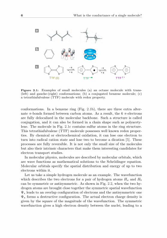
Shown in Fig. 2.1 are some examples of small molecules which have typ-ical length of 1 nm. An alkane molecule (Fig. 2.1a) has a simple structurecontaining only carbon and hydrogen atoms. Due to the rotation of thecarbon-carbon sigma bond, an alkane molecule can have trans- and gauche-
5
6 What is the conductance of a single molecule?
S
S
S
S
S
S
S
S
S
S
S
S- e
+ e
TTF (0) TTF + TTF 2 +
- e
+ e
b
a
c
Figure 2.1: Examples of small molecules (a) an octane molecule with trans-(left) and gauche-(right) conformations; (b) a conjugated benzene molecule; (c)a tetrathiafulvalene (TTF) molecule with redox property.
conformations. In a benzene ring (Fig. 2.1b), there are three extra alter-nate π-bonds formed between carbon atoms. As a result, the 6 π-electronsare fully delocalized in the molecular backbone. Such a structure is calledconjugation, and it can also be formed in a chain shape such as polyacety-lene. The molecule in Fig. 2.1c contains sulfur atoms in the ring structure.This tetrathiafulvalene (TTF) molecule possesses well known redox proper-ties. By chemical or electrochemical oxidation, it can lose one electron toturn into radical cation state and lose two to become a dication [5]. Theseprocesses are fully reversible. It is not only the small size of the moleculesbut also their intrinsic characters that make them interesting candidates forelectron transport studies.
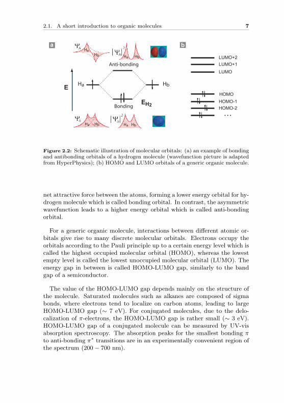
In molecular physics, molecules are described by molecular orbitals, whichare wave functions as mathematical solutions to the Schrodinger equation.Molecular orbitals specify the spatial distribution and energy of up to twoelectrons within it.
Let us take a simple hydrogen molecule as an example. The wavefunctionwhich describes the two electrons for a pair of hydrogen atoms Ha and Hb
can be symmetric or antisymmetric. As shown in Fig. 2.2, when the two hy-drogen atoms are brought close together the symmetric spatial wavefunctionΨs leads to an overlap configuration of electrons and the antisymmetric oneΨa forms a destructive configuration. The actual electron charge density isgiven by the square of the magnitude of the wavefunction. The symmetricwavefunction gives a high electron density between the nuclei, leading to a
2.1. A short introduction to organic molecules 7
HbHa
EH2
E
LUMO
HOMO
Bonding
LUMO+1 LUMO+2
HOMO-1HOMO-2
HaHb
HbHa
Ha Hb
Ha Hb
Anti-bonding
. . .
ba
Figure 2.2: Schematic illustration of molecular orbitals: (a) an example of bondingand antibonding orbitals of a hydrogen molecule (wavefunction picture is adaptedfrom HyperPhysics); (b) HOMO and LUMO orbitals of a generic organic molecule.
net attractive force between the atoms, forming a lower energy orbital for hy-drogen molecule which is called bonding orbital. In contrast, the asymmetricwavefunction leads to a higher energy orbital which is called anti-bondingorbital.
For a generic organic molecule, interactions between different atomic or-bitals give rise to many discrete molecular orbitals. Electrons occupy theorbitals according to the Pauli principle up to a certain energy level which iscalled the highest occupied molecular orbital (HOMO), whereas the lowestempty level is called the lowest unoccupied molecular orbital (LUMO). Theenergy gap in between is called HOMO-LUMO gap, similarly to the bandgap of a semiconductor.
The value of the HOMO-LUMO gap depends mainly on the structure ofthe molecule. Saturated molecules such as alkanes are composed of sigmabonds, where electrons tend to localize on carbon atoms, leading to largeHOMO-LUMO gap (∼ 7 eV). For conjugated molecules, due to the delo-calization of π-electrons, the HOMO-LUMO gap is rather small (∼ 3 eV).HOMO-LUMO gap of a conjugated molecule can be measured by UV-visabsorption spectroscopy. The absorption peaks for the smallest bonding πto anti-bonding π∗ transitions are in an experimentally convenient region ofthe spectrum (200− 700 nm).
8 What is the conductance of a single molecule?
2.2 Conductance quantization of an atomic-sizedjunction
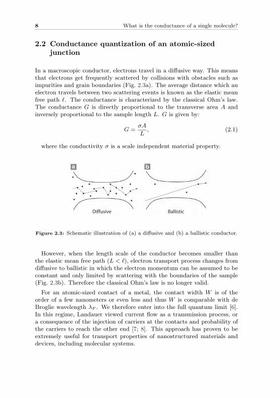
In a macroscopic conductor, electrons travel in a diffusive way. This meansthat electrons get frequently scattered by collisions with obstacles such asimpurities and grain boundaries (Fig. 2.3a). The average distance which anelectron travels between two scattering events is known as the elastic meanfree path `. The conductance is characterized by the classical Ohm’s law.The conductance G is directly proportional to the transverse area A andinversely proportional to the sample length L. G is given by:
G =σA
L, (2.1)
where the conductivity σ is a scale independent material property.
Diffusive Ballistic
ba
Figure 2.3: Schematic illustration of (a) a diffusive and (b) a ballistic conductor.
However, when the length scale of the conductor becomes smaller thanthe elastic mean free path (L < `), electron transport process changes fromdiffusive to ballistic in which the electron momentum can be assumed to beconstant and only limited by scattering with the boundaries of the sample(Fig. 2.3b). Therefore the classical Ohm’s law is no longer valid.
For an atomic-sized contact of a metal, the contact width W is of theorder of a few nanometers or even less and thus W is comparable with deBroglie wavelength λF . We therefore enter into the full quantum limit [6].In this regime, Landauer viewed current flow as a transmission process, ora consequence of the injection of carriers at the contacts and probability ofthe carriers to reach the other end [7; 8]. This approach has proven to beextremely useful for transport properties of nanostructured materials anddevices, including molecular systems.
2.2. Conductance quantization of an atomic-sized junction 9
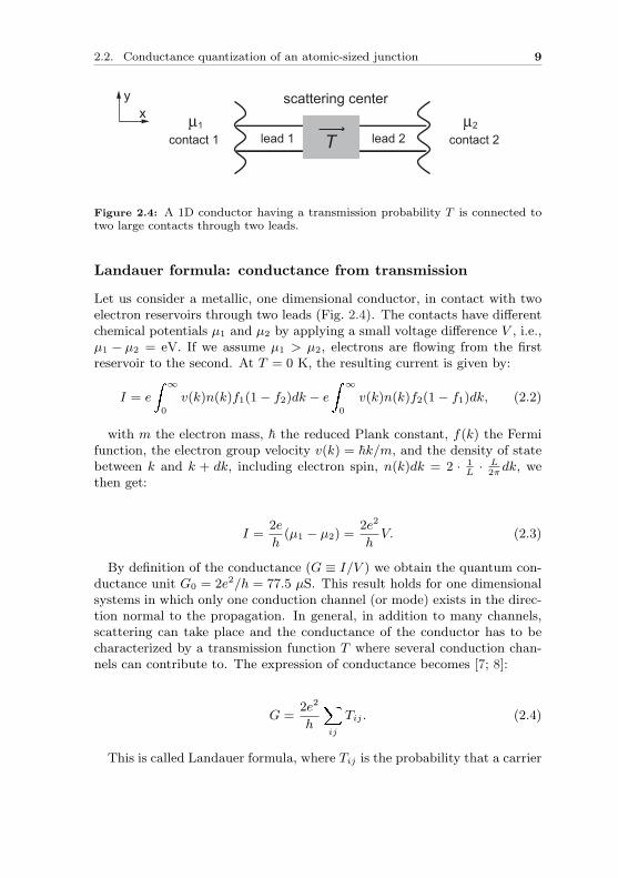
µ1 µ2lead 1 lead 2contact 1 contact 2
scattering center
T
xy
Figure 2.4: A 1D conductor having a transmission probability T is connected totwo large contacts through two leads.
Landauer formula: conductance from transmission
Let us consider a metallic, one dimensional conductor, in contact with twoelectron reservoirs through two leads (Fig. 2.4). The contacts have differentchemical potentials µ1 and µ2 by applying a small voltage difference V , i.e.,µ1 − µ2 = eV. If we assume µ1 > µ2, electrons are flowing from the firstreservoir to the second. At T = 0 K, the resulting current is given by:
I = e
Z ∞
0
v(k)n(k)f1(1− f2)dk − e
Z ∞
0
v(k)n(k)f2(1− f1)dk, (2.2)
with m the electron mass, ~ the reduced Plank constant, f(k) the Fermifunction, the electron group velocity v(k) = ~k/m, and the density of statebetween k and k + dk, including electron spin, n(k)dk = 2 · 1
L· L
2πdk, we
then get:
I =2e
h(µ1 − µ2) =
2e2
hV. (2.3)
By definition of the conductance (G ≡ I/V ) we obtain the quantum con-ductance unit G0 = 2e2/h = 77.5 µS. This result holds for one dimensionalsystems in which only one conduction channel (or mode) exists in the direc-tion normal to the propagation. In general, in addition to many channels,scattering can take place and the conductance of the conductor has to becharacterized by a transmission function T where several conduction chan-nels can contribute to. The expression of conductance becomes [7; 8]:
G =2e2
h
Xij
Tij . (2.4)
This is called Landauer formula, where Tij is the probability that a carrier
10 What is the conductance of a single molecule?
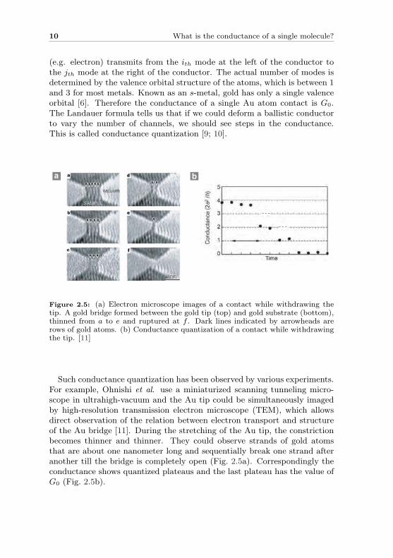
(e.g. electron) transmits from the ith mode at the left of the conductor tothe jth mode at the right of the conductor. The actual number of modes isdetermined by the valence orbital structure of the atoms, which is between 1and 3 for most metals. Known as an s-metal, gold has only a single valenceorbital [6]. Therefore the conductance of a single Au atom contact is G0.The Landauer formula tells us that if we could deform a ballistic conductorto vary the number of channels, we should see steps in the conductance.This is called conductance quantization [9; 10].
b ba
Figure 2.5: (a) Electron microscope images of a contact while withdrawing thetip. A gold bridge formed between the gold tip (top) and gold substrate (bottom),thinned from a to e and ruptured at f . Dark lines indicated by arrowheads arerows of gold atoms. (b) Conductance quantization of a contact while withdrawingthe tip. [11]
Such conductance quantization has been observed by various experiments.For example, Ohnishi et al. use a miniaturized scanning tunneling micro-scope in ultrahigh-vacuum and the Au tip could be simultaneously imagedby high-resolution transmission electron microscope (TEM), which allowsdirect observation of the relation between electron transport and structureof the Au bridge [11]. During the stretching of the Au tip, the constrictionbecomes thinner and thinner. They could observe strands of gold atomsthat are about one nanometer long and sequentially break one strand afteranother till the bridge is completely open (Fig. 2.5a). Correspondingly theconductance shows quantized plateaus and the last plateau has the value ofG0 (Fig. 2.5b).
2.2. Conductance quantization of an atomic-sized junction 11
An explanation of the overall resistance
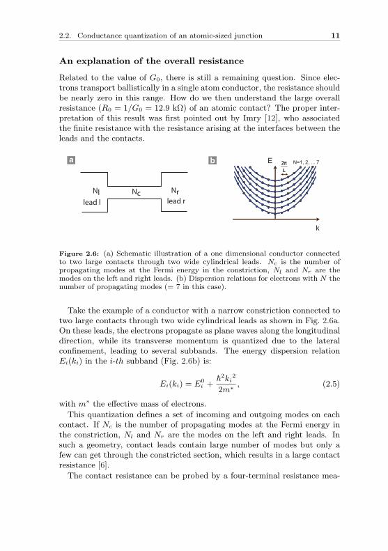
Related to the value of G0, there is still a remaining question. Since elec-trons transport ballistically in a single atom conductor, the resistance shouldbe nearly zero in this range. How do we then understand the large overallresistance (R0 = 1/G0 = 12.9 kΩ) of an atomic contact? The proper inter-pretation of this result was first pointed out by Imry [12], who associatedthe finite resistance with the resistance arising at the interfaces between theleads and the contacts.
Nl NrNclead l lead r
k
E 2πL
2πL
ba N=1, 2, ... 7
Figure 2.6: (a) Schematic illustration of a one dimensional conductor connectedto two large contacts through two wide cylindrical leads. Nc is the number ofpropagating modes at the Fermi energy in the constriction, Nl and Nr are themodes on the left and right leads. (b) Dispersion relations for electrons with N thenumber of propagating modes (= 7 in this case).
Take the example of a conductor with a narrow constriction connected totwo large contacts through two wide cylindrical leads as shown in Fig. 2.6a.On these leads, the electrons propagate as plane waves along the longitudinaldirection, while its transverse momentum is quantized due to the lateralconfinement, leading to several subbands. The energy dispersion relationEi(ki) in the i-th subband (Fig. 2.6b) is:
Ei(ki) = E0i +
~2ki2
2m∗ , (2.5)
with m∗ the effective mass of electrons.
This quantization defines a set of incoming and outgoing modes on eachcontact. If Nc is the number of propagating modes at the Fermi energy inthe constriction, Nl and Nr are the modes on the left and right leads. Insuch a geometry, contact leads contain large number of modes but only afew can get through the constricted section, which results in a large contactresistance [6].
The contact resistance can be probed by a four-terminal resistance mea-
12 What is the conductance of a single molecule?
surement. Picciotto et al. have reported that ballistic 1D wires of 2Delectron gas indeed show a vanishing resistance [13]. This demonstratesexperimentally that the high resistance values observed in two-probe mea-surements on such systems originate from the contacts alone, and that theintrinsic resistance is negligible.
2.3 Modeling the conductance of a molecular junction
If a metallic point contact breaks and separates to form a pair of atomicallysharp tips, these tips can be used as electrical contacts to small molecules.Practically molecules are usually designed to have terminal linker groupswhich allow to bind chemically to electrodes to form metal-molecule-metaljunctions. It is then possible to measure their transport properties. We willintroduce several models here to describe the conductance of a molecularjunction.
2.3.1 Single molecules as electron tunneling barrier
In this model a single molecule is sandwiched between two metal contacts.The role of the molecule is considered as tunneling barrier for electron trans-port. It is also called superexchange model [14; 15].
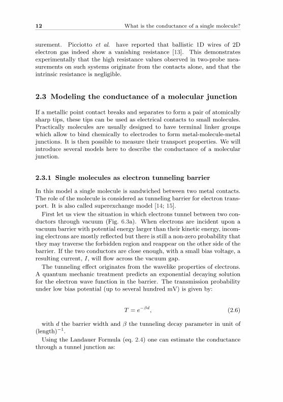
First let us view the situation in which electrons tunnel between two con-ductors through vacuum (Fig. 6.3a). When electrons are incident upon avacuum barrier with potential energy larger than their kinetic energy, incom-ing electrons are mostly reflected but there is still a non-zero probability thatthey may traverse the forbidden region and reappear on the other side of thebarrier. If the two conductors are close enough, with a small bias voltage, aresulting current, I, will flow across the vacuum gap.
The tunneling effect originates from the wavelike properties of electrons.A quantum mechanic treatment predicts an exponential decaying solutionfor the electron wave function in the barrier. The transmission probabilityunder low bias potential (up to several hundred mV) is given by:
T = e−βd, (2.6)
with d the barrier width and β the tunneling decay parameter in unit of(length)−1.
Using the Landauer Formula (eq. 2.4) one can estimate the conductancethrough a tunnel junction as:
2.3. Modeling the conductance of a molecular junction 13
EF
d
eV
Φ
Vacuum Level
2
l
LUMO
HOMO
Scource Drain Scource Drain
EFeV2
ψ
ba
Figure 2.7: Schematic of electron tunneling through: (a) vacuum; and (b) a 1,4-benzene dithiol molecule.
G = G0 · e−βd; with β =2q
2m(Φ− eV2
)
~, (2.7)
where m is the electron mass, Φ is the local tunneling barrier height invacuum (= work function for metals), V is the applied bias voltage betweenthe two contacts. If the applied voltage is much smaller than the workfunction (eV Φ), the tunneling decay parameter can be simplified to
β = 2√
2mΦ~ .
Taking a work function value for gold 5.0 eV, the decay factor for electrons
tunneling in vacuum is βvacumm = 1.025√
Φ [eV−0.5A−1] = 2.3 A−1
.
As an example, a 1,4-benzene dithiol molecule can be sandwiched betweensource and drain electrodes as shown in Fig. 6.3b. The molecule has defineddiscrete energy levels (the most important levels for transport are HOMOand LUMO orbitals). The conductance Gmol can in analogy be written as[16]:
Gmol = A · e−βl; with β =2√
2m∗Φ∗
~, (2.8)
where l is the length of molecule, m∗ is the effective electron mass andΦ∗ is the effective tunneling barrier height. The prefactor A depends on theelectron density-of-states at the point where the molecule contacts the goldelectrode. Instead of the work function in vacuum, the tunneling barrieramounts to the closest molecular level related to EF of the metal [17; 18],
14 What is the conductance of a single molecule?
i.e. Φ∗ = (EF − ELUMO) or Φ∗ = (EHUMO − EF ). For a simple estima-tion that EF locates in the middle of HOMO-LUMO gap and there is nobroadening and charging effects, the tunneling barrier Φ∗ can be written asΦ∗ ' (EHOMO − ELUMO)/2.
As mentioned before, conjugated molecules (Fig. 2.1b) have smaller HOMO-LUMO gap than saturated molecules (Fig. 2.1a), therefore lower tunneling
decay factor (∼ 0.3 A−1
) compared with saturated alkanes (∼ 1 A−1
).
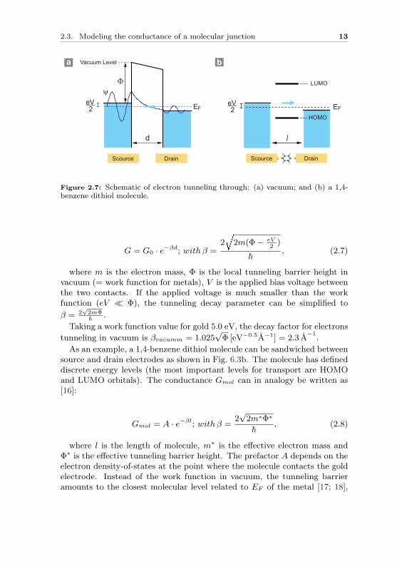
2.3.2 Electron hopping through a single molecule
EF
µ2
µ1eV2
e-e-
Figure 2.8: The model of electron hopping through the states of a long molecularwire.
When the length of molecular bridges increases, the charge transportmechanism changes then from direct tunneling to hopping. For a long mole-cular “wire”, electrons dwell on several molecular orbital states and thetransport is therefore incoherent. This is evidenced by a change in the lengthdependence of the electron transfer rate [19]. Specifically, for short bridges,the length dependence is exponential according to tunneling as discussedin Section 2.3.1. For long bridges with hopping mechanism, the scaling islinear. Furthermore, the two mechanisms show different behaviors on tem-perature dependence: The tunneling process is temperature independent,while hopping is strongly thermally activated.
Experimentally, the transition between the two mechanisms can be ob-served by measuring the conductance change of molecular junctions withdifferent molecular length built by the same repetition unit and at differenttemperatures. A metal-coated atomic force microscope (AFM) techniquewas used to measure the resistance and current-voltage characteristics ofconjugated molecular wires ranging in length from 1 to 7 nm. The tunnel-ing to hopping transition was observed at the length of ∼ 4 nm. [20]
2.3. Modeling the conductance of a molecular junction 15
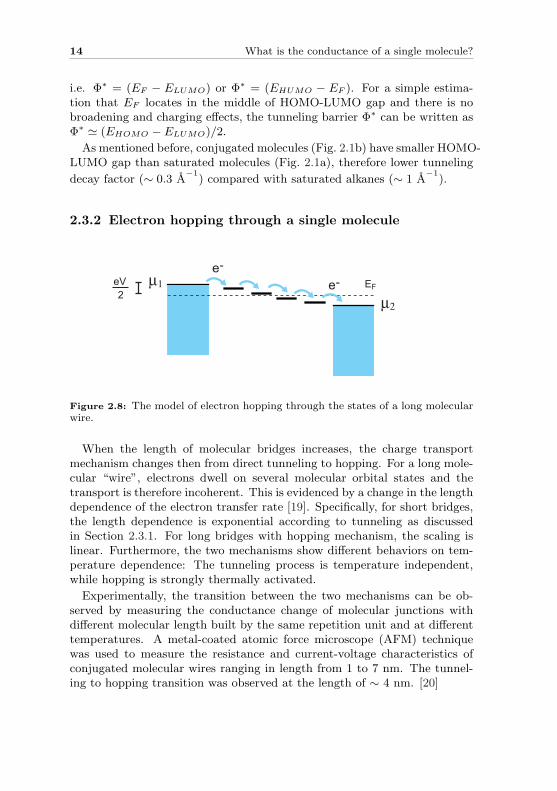
2.3.3 Resonant double barrier tunneling model
In this model a single molecule sandwiched between two metal electrodes isrepresented by one energy level. The electron transport can be calculated byusing simple kinetic equations. However when a molecule binds chemicallyto electrodes through terminal linker groups, the molecule can not be treatedas an isolated system as in vacuum anymore. The coupling of the moleculeto electrodes leads not only to the broadening but also to a shift of themolecular energy levels. These aspects will be discussed in the followingsections.
Single level model
A simple resonant tunneling model [21] can be introduced by consideringonly one discrete molecular energy level ε being close to the Fermi energyEF (Fig. 2.9).
EF
Γ1Γ2
e-e-e-eV
2µ1
µ2ε
Figure 2.9: The model of electron tunneling through a double barrier Γ1 and Γ2.The molecule is represented by one discrete molecular energy level ε being close tothe Fermi energy EF and it is broadened by coupling to electrodes.
Unlike the superexchange model as described in Section 2.3.1, here elec-trons at this resonant energy level ε can cross the double barrier withoutbeing reflected. The current through the level can then be derived se-quentially. The numbers of electrons occupying the level would be givenby N1 = 2f(ε, µ1) if the level is in equilibrium with the left contact andby N2 = 2f(ε, µ2) in equilibrium with the right one. The factor 2 comesfrom the spin degeneracy, and f(ε, µi) is the Fermi-Dirac function. In non-equilibrium, the number N of electrons in the level will be somewhere inbetween N1 and N2. We can write the resulting current from the left con-
16 What is the conductance of a single molecule?
tact to the molecule:
I1 =eΓ1
~(N1 −N), (2.9)
and from the molecule to the right contact as:
I2 =eΓ2
~(N −N2). (2.10)
Γ1 and Γ2 have the dimension of energy, denoting the coupling between thecontacts and the level. Γ1/~ and Γ2/~ have the dimension of s−1. They arethe rates at which an electron will escape initially from the source contact tothe level ε and from the level to drain contacts respectively. In equilibrium,I1 must be equal to I2 so that
N =N1Γ1 + N2Γ2
Γ1 + Γ2, (2.11)
and finally we get the net current:
I = I1 = I2 =2e
~Γ1Γ2
Γ1 + Γ2[f(ε, µ1)− f(ε, µ2)]. (2.12)
Knowing the energy level ε, the coupling factors Γ1, Γ2 and the electrochem-ical potentials µ1, µ2 of the two contacts, we can calculate the current I fromeq. 2.12.
This simple result serves to illustrate certain basic facts about the processof current flow. Firstly, no current will flow if f(ε, µ1) = f(ε, µ2). A levelε that is way below both electrochemical potentials µ1 and µ1 will havef(ε, µ1) = f(ε, µ2) = 1, and way above both potentials, f(ε, µ1) = f(ε, µ2)= 0. In both cases, the level ε will not contribute to the current. It is onlywhen the level lies within a few kBT of the potentials µ1 and µ2 that wehave f(ε, µ1) 6= f(ε, µ2). Contact 1 keeps pumping in electrons and contact2 keeps pulling them out, resulting a continuous transfer of electrons fromcontact 1 to 2 corresponding to a current I in the external circuit.
Broadening of molecular levels
For a metal-molecule-metal junction, if the molecule is strongly coupled tothe metallic contacts, the molecular orbitals and the electronic states of theleads can overlap. This leads to a hybridization of the electronic states, andtherefore a common delocalized electronic wave function extending over thewhole junction. In consequence the density of states D(E) (the probabilityof having an electron state with energy E) can not be described anymoreby a Dirac delta function at energy ε. The total broadening of the single
2.3. Modeling the conductance of a molecular junction 17
energy level is Γ = Γ1 +Γ2 and is better represented by a Lorentzian densityof states [21] as shown in Fig. 2.9:
D(E) =1
2π
Γ
(E − ε)2 + (Γ/2)2. (2.13)
Including this in eq. 2.12 and integrating over the energy we finally obtainthe current:
I =2e
~
Z ∞
−∞dE T (E)[f(ε, µ1)− f(ε, µ2)], (2.14)
where the transmission function T is defined as:
T (E) = 2πD(E)Γ1Γ2
Γ1 + Γ2=
Γ1Γ2
(E − ε)2 + (Γ1 + Γ2)2/4. (2.15)
At low temperatures, we can rewrite eq. 2.14 as:
I =2e
h
Z µ
−µ
dE T (E), (2.16)
with µ = +eV/2 and −µ = −eV/2. In the linear regime (eV → 0), theexpression for the conductance is then
G =2e2
h
Γ1Γ2
(E − ε)2 + (Γ1 + Γ2)2/4. (2.17)
Charging effects
When a molecule is chemically bonded to metal electrodes, a partial charge-transfer takes place even without having an applied bias voltage. Therefore,the charge on the molecule differs from that of an isolated molecule in vac-uum. The additional charging energy, Uc describes how the molecular levelsare shifted in energy by a contact potential due to electrons lost or gainedby the molecule upon coupling to the leads. The molecular level is thereforeshifted to ε′:
ε′ = ε + Uc, (2.18)
18 What is the conductance of a single molecule?
with ε being the energy level of the isolated molecule. This modifiedenergy can be inserted into eq. 2.13 to express the density of states includingcharging effects:
D(E) =1
2π
Γ
(E − ε− Uc)2 + (Γ/2)2. (2.19)
Depending on the coupling term Γ, D(E) can deviate significantly fromthe ideal shape of Lorentzian distribution. If the molecule is weakly cou-pled to the metallic contacts (Γ Uc), the junction behaves as a capaci-tor. After one electron tunnels onto the molecule, the capacitor is chargedwith charging energy EC = e2/2C. If the capacitance is very small, theenergy buildup can be large enough to prevent another electron from tun-neling in. The electrical current is then suppressed at low bias voltages andcharge transport occurs in integer values of the charge quantum e. It iscalled Coulomb blockade. This phenomenon can be observed at tempera-tures where the characteristic charging energy is larger than the thermalenergy of the charge carriers (EC > kBT ).
Chapter 3
MCBJ: Making electrical contacts
to single molecules
To determine the electronic properties of molecular junctions, molecules needto be wired between a source and a drain electrode. It is a real experimentalchallenge to form stable and reproducible contacts with defined spacing onthe 1 nm scale without damaging or altering the molecules.
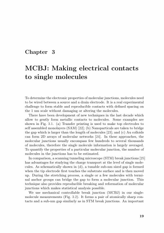
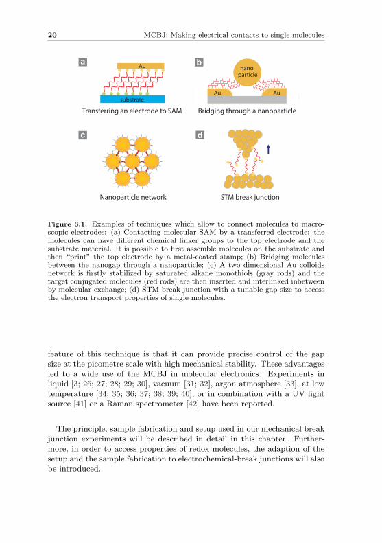
There have been development of new techniques in the last decade whichallow to gently form metallic contacts to molecules. Some examples areshown in Fig. 3.1. (a) Transfer printing is used to make top electrodes toself assembled monolayers (SAM) [22]; (b) Nanoparticals are taken to bridgethe gap which is larger than the length of molecules [23]; and (c) Au colloidscan form 2D arrays of molecular networks [24]. In these approaches, themolecular junctions usually encompass few hundreds to several thousandsof molecules, therefore the single molecule information is largely averaged.To quantify the properties of a particular molecular junction, the number ofmolecules in the junctions has to be estimated.
In comparison, a scanning tunneling microscope (STM) break junctions [25]has advantages for studying the charge transport at the level of single mole-cules. As schematically shown in (d), a tunable sub-nm sized gap is formedwhen the tip electrode first touches the substrate surface and is then movedup. During the stretching process, a single or a few molecules with termi-nal anchor groups can bridge the gap to form a molecular junction. Thistechnique also provides reproducible breaking and reformation of molecularjunctions which makes statistical analysis possible.
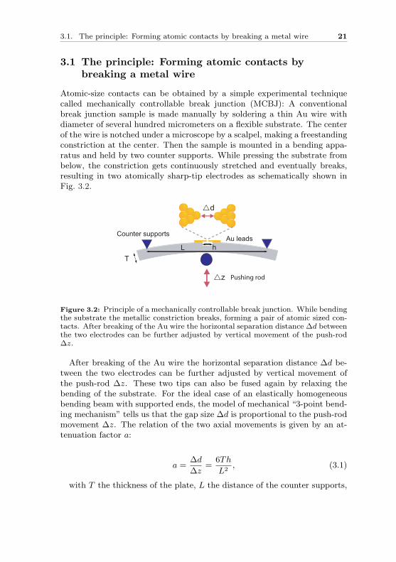
We use mechanical controllable break junction (MCBJ) in our single-molecule measurements (Fig. 3.2). It forms a pair of atomically sharp con-tacts and a sub-nm gap similarly as in STM break junctions. An important
19
20 MCBJ: Making electrical contacts to single molecules
a
Au
substrate
Transferring an electrode to SAM
b
nanoparticle
Au Au
Bridging through a nanoparticle
c
Nanoparticle network
d
STM break junction
Figure 3.1: Examples of techniques which allow to connect molecules to macro-scopic electrodes: (a) Contacting molecular SAM by a transferred electrode: themolecules can have different chemical linker groups to the top electrode and thesubstrate material. It is possible to first assemble molecules on the substrate andthen “print” the top electrode by a metal-coated stamp; (b) Bridging moleculesbetween the nanogap through a nanoparticle; (c) A two dimensional Au colloidsnetwork is firstly stabilized by saturated alkane monothiols (gray rods) and thetarget conjugated molecules (red rods) are then inserted and interlinked inbetweenby molecular exchange; (d) STM break junction with a tunable gap size to accessthe electron transport properties of single molecules.
feature of this technique is that it can provide precise control of the gapsize at the picometre scale with high mechanical stability. These advantagesled to a wide use of the MCBJ in molecular electronics. Experiments inliquid [3; 26; 27; 28; 29; 30], vacuum [31; 32], argon atmosphere [33], at lowtemperature [34; 35; 36; 37; 38; 39; 40], or in combination with a UV lightsource [41] or a Raman spectrometer [42] have been reported.
The principle, sample fabrication and setup used in our mechanical breakjunction experiments will be described in detail in this chapter. Further-more, in order to access properties of redox molecules, the adaption of thesetup and the sample fabrication to electrochemical-break junctions will alsobe introduced.
3.1. The principle: Forming atomic contacts by breaking a metal wire 21
3.1 The principle: Forming atomic contacts bybreaking a metal wire
Atomic-size contacts can be obtained by a simple experimental techniquecalled mechanically controllable break junction (MCBJ): A conventionalbreak junction sample is made manually by soldering a thin Au wire withdiameter of several hundred micrometers on a flexible substrate. The centerof the wire is notched under a microscope by a scalpel, making a freestandingconstriction at the center. Then the sample is mounted in a bending appa-ratus and held by two counter supports. While pressing the substrate frombelow, the constriction gets continuously stretched and eventually breaks,resulting in two atomically sharp-tip electrodes as schematically shown inFig. 3.2.
Au leadsCounter supports
L hT
z Pushing rod
d
Figure 3.2: Principle of a mechanically controllable break junction. While bendingthe substrate the metallic constriction breaks, forming a pair of atomic sized con-tacts. After breaking of the Au wire the horizontal separation distance ∆d betweenthe two electrodes can be further adjusted by vertical movement of the push-rod∆z.
After breaking of the Au wire the horizontal separation distance ∆d be-tween the two electrodes can be further adjusted by vertical movement ofthe push-rod ∆z. These two tips can also be fused again by relaxing thebending of the substrate. For the ideal case of an elastically homogeneousbending beam with supported ends, the model of mechanical “3-point bend-ing mechanism” tells us that the gap size ∆d is proportional to the push-rodmovement ∆z. The relation of the two axial movements is given by an at-tenuation factor a:
a =∆d
∆z=
6Th
L2, (3.1)
with T the thickness of the plate, L the distance of the counter supports,
22 MCBJ: Making electrical contacts to single molecules
and h the free-standing width of the Au wire.The attenuation factor a is an important parameter. It has a large influ-
ence on the mechanical stability. A small factor provides higher immunityto external vibrations and more precise control on the size of the horizontalgap. To reduce the attenuation factor, we have used micro-fabricated breakjunction samples.
3.1.1 Micro-fabricated break junction samples
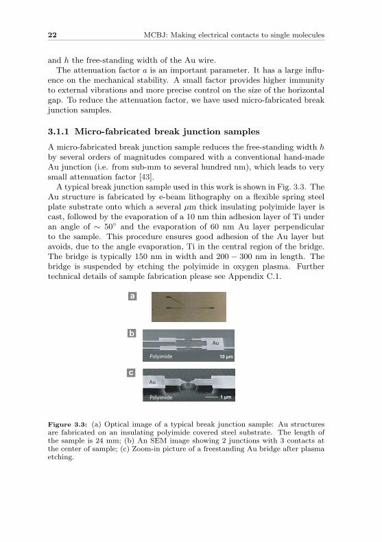
A micro-fabricated break junction sample reduces the free-standing width hby several orders of magnitudes compared with a conventional hand-madeAu junction (i.e. from sub-mm to several hundred nm), which leads to verysmall attenuation factor [43].
A typical break junction sample used in this work is shown in Fig. 3.3. TheAu structure is fabricated by e-beam lithography on a flexible spring steelplate substrate onto which a several µm thick insulating polyimide layer iscast, followed by the evaporation of a 10 nm thin adhesion layer of Ti underan angle of ∼ 50 and the evaporation of 60 nm Au layer perpendicularto the sample. This procedure ensures good adhesion of the Au layer butavoids, due to the angle evaporation, Ti in the central region of the bridge.The bridge is typically 150 nm in width and 200 − 300 nm in length. Thebridge is suspended by etching the polyimide in oxygen plasma. Furthertechnical details of sample fabrication please see Appendix C.1.
10 μm
Au
Polyimide
Au
a
b
c
Polyimide 1 μm
Figure 3.3: (a) Optical image of a typical break junction sample: Au structuresare fabricated on an insulating polyimide covered steel substrate. The length ofthe sample is 24 mm; (b) An SEM image showing 2 junctions with 3 contacts atthe center of sample; (c) Zoom-in picture of a freestanding Au bridge after plasmaetching.
3.2. The setup 23
3.1.2 Discussion on the attenuation factor
We can estimate the theoretical attenuation factor based on the geometryand the size of our break junction sample according to eq. 3.1. With thethickness of the substrate T = 0.3 mm, the distance between the countersupports L = 20 mm and the length of the free standing bridge h ≈ 0.3µm, we get a ≈ 1 · 10−6. However, in practice, the sample usually doesnot deform elastically. The plastic deformation of the sample results in anincrease of attenuation factor a by approximately one order of magnitude[44].
Experimentally one can perform a calibration for attenuation factor (ac)by measuring the variation of the tunneling current I with the gap sepa-ration d in vacuum [26; 45]. The expression for the tunneling current atlow bias voltage through a square barrier of height Φ and thickness d is:I ∝ exp(−2d
√2mΦ/~), in which the horizontal separation d is related to
the vertical movement of z by d = ac(z − z0). If we use the measuredslope of lnI as a function of z (lnI ∝ −(2a
√2mΦ/~)z) and fix the work
function of Au Φvacuum to the established value of 3.5 − 5.0 eV [46], weget ac = 1.6 − 4 · 10−5 for the micro-fabricated break junction samples.This means that a vertical pushrod movement of 10 µm corresponds onlyto 2− 7 A separation of the two electrodes. These atomic contacts and thecontrollable sub nm-sized gap are ideal for single molecule measurements.
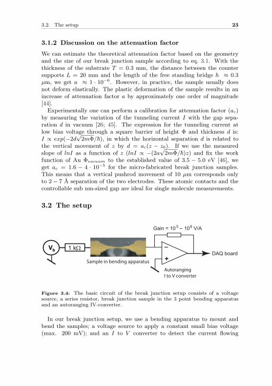
3.2 The setup
1 kΩVb
Gain = 105 – 108 V/A
1 kΩVb
Gain = 10 – 10 V/A
DAQ board
5 8
Sample in bending apparatus
AutorangingI to V converter
_
+
Figure 3.4: The basic circuit of the break junction setup consists of a voltagesource, a series resistor, break junction sample in the 3 point bending apparatusand an autoranging IV-converter.
In our break junction setup, we use a bending apparatus to mount andbend the samples; a voltage source to apply a constant small bias voltage(max. 200 mV); and an I to V converter to detect the current flowing
24 MCBJ: Making electrical contacts to single molecules
through the Au bridge during its breaking process. It is important to havean autoranging IV -converter which can quickly change the gain over sev-eral decades because after breaking of the Au bridge, the tunneling currentdecays from mA to nA exponentially with respect to the tip separation.The circuit is completed by a series resistor (1 kΩ) to limit the maximumcurrent and protect the original Au bridge (which has typical resistance of∼ 200Ω). The data is recorded by a data acquisition board (DAQ) con-nected to a computer (Fig. 3.4). In order to measure organic molecules in achemical environment, a liquid cell is added to the setup. These parts willbe explained separately in the following pages.
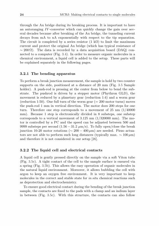
3.2.1 The bending apparatus
To perform a break junction measurement, the sample is hold by two countersupports on the side, positioned at a distance of 20 mm (Fig. 3.5 Sampleholder). A push-rod is pressing at the center from below to bend the sub-strate. The pushrod is driven by a stepper motor (Phythron GLD), themovement is reduced by a planetary gear (reduction 1:4) and a worm gear(reduction 1:50). One full turn of the worm gear (= 200 motor turns) movesthe push-rod 1 mm in vertical direction. The motor does 200 steps for oneturn. Therefore one step corresponds to a movement of 25 nm (1/40000mm). Because 1 step is electronically divided in 8 substeps, one substepcorresponds to a vertical movement of 3.125 nm (1/320000 mm). The mo-tor is controlled by a PC and the speed can be adjusted between 500 and9999 substeps per second (1.56− 31.2 µm/s). To fully open/close the breakjunction 10-20 motor rotations (∼ 200− 400 µm) are needed. Piezo actua-tors are not able to perform such long distances (typically max. ∼ 100 µm)and therefore it is not considered in our setup [26].
3.2.2 The liquid cell and electrical contacts
A liquid cell is gently pressed directly on the sample via a soft Viton tube(Fig. 3.5c). A tight contact of the cell to the sample surface is ensured viaa spring (Fig. 3.5b). This allows the easy operation of organic molecules inthe natural liquid environment. Moreover, it allows bubbling the cell withargon to keep an oxygen free environment. It is very important to keepmolecules in the correct and stable state for in situ chemical reactions suchas deprotection and electrochemistry.
To ensure good electrical contact during the bending of the break junctionsample, the contacts are fixed to the pads with a clamp and an indium layerin between (Fig. 3.5c). With this structure, the contacts can also follow
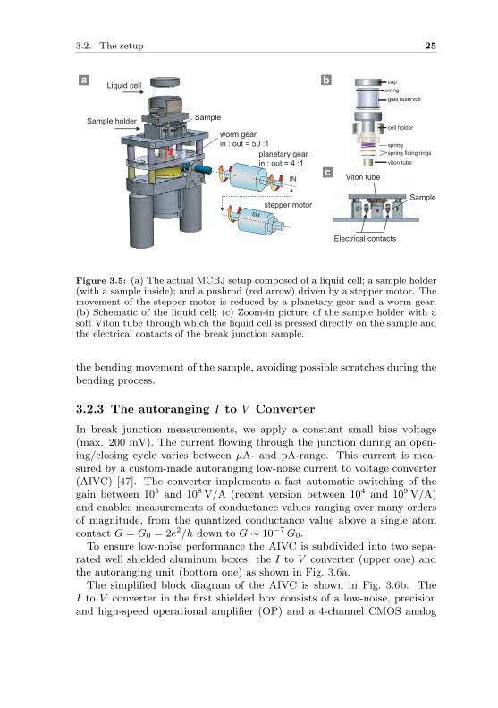
3.2. The setup 25
SM
zz
Sample
worm gearin : out = 50 :1
planetary gearin : out = 4 :1
stepper motor
IN
Sample
cap
glas reservoiro-ring
viton tube
spring fixing ringsspring
cell holder
Liquid cell
Sample holder
Viton tube
Electrical contacts
a b
c
Figure 3.5: (a) The actual MCBJ setup composed of a liquid cell; a sample holder(with a sample inside); and a pushrod (red arrow) driven by a stepper motor. Themovement of the stepper motor is reduced by a planetary gear and a worm gear;(b) Schematic of the liquid cell; (c) Zoom-in picture of the sample holder with asoft Viton tube through which the liquid cell is pressed directly on the sample andthe electrical contacts of the break junction sample.
the bending movement of the sample, avoiding possible scratches during thebending process.
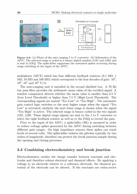
3.2.3 The autoranging I to V Converter
In break junction measurements, we apply a constant small bias voltage(max. 200 mV). The current flowing through the junction during an open-ing/closing cycle varies between µA- and pA-range. This current is mea-sured by a custom-made autoranging low-noise current to voltage converter(AIVC) [47]. The converter implements a fast automatic switching of thegain between 105 and 108 V/A (recent version between 104 and 109 V/A)and enables measurements of conductance values ranging over many ordersof magnitude, from the quantized conductance value above a single atomcontact G = G0 = 2e2/h down to G ∼ 10−7 G0.
To ensure low-noise performance the AIVC is subdivided into two sepa-rated well shielded aluminum boxes: the I to V converter (upper one) andthe autoranging unit (bottom one) as shown in Fig. 3.6a.
The simplified block diagram of the AIVC is shown in Fig. 3.6b. TheI to V converter in the first shielded box consists of a low-noise, precisionand high-speed operational amplifier (OP) and a 4-channel CMOS analog
26 MCBJ: Making electrical contacts to single molecules
VoutSpikeKiller
I in
I to V Converter
Auto-Ranging Unit
a b
Figure 3.6: (a) Photo of the auto ranging I to V converter. (b) Schematics of theAIVC. The selected range is coded in a binary digital number (LR1 and LR0) andis sent to DAQ. The spike-killer suppresses the unwanted spikes occurring duringrange switching at the input of the AIVC.
multiplexer (MUX) which has four different feedback resistors (0.1 MΩ, 1MΩ, 10 MΩ and 100 MΩ) which correspond to the four decades of gain: 105,106, 107 and 108 V/A.
The auto-ranging unit is installed in the second shielded box. A 70 Hzlow pass filter provides the arithmetic mean value of the rectified signal. Awindow comparator detects whether the mean value is smaller than 0.5 V(Low Level Threshold) or higher than 7.5 V (High Level Threshold). Thecorresponding signals are named “Too Low” or “Too High”. The automaticgain control logic switches to the next higher range when the signal “TooLow” is activated; similarly the next lower range is chosen when the signal“Too High” is active. The selected range is binary coded in the two signalsLR1, LR0. These digital range signals are sent to the I to V converter toselect the right feedback resistor as well as to the DAQ to record the gain.
Prior to the input of the AIVC, a spike-killer (SK) is mounted in orderto reduce voltage spikes generated by the AIVC during switching betweendifferent gain ranges. On high impedance sources these spikes can reachlevels of several volts. The spike-killer reduces the glitches typically by twoorders of magnitude, therefore can protect the break junction sample duringthe opening and closing processes.
3.3 Combining electrochemistry and break junction
Electrochemistry studies the charge transfer between reactants and elec-trodes and therefore relates electrical and chemical effects. By applying avoltage to an electrode relative to a reference electrode, the chemical po-tential of the electrode can be altered. If the reactants are redox-active
3.3. Combining electrochemistry and break junction 27
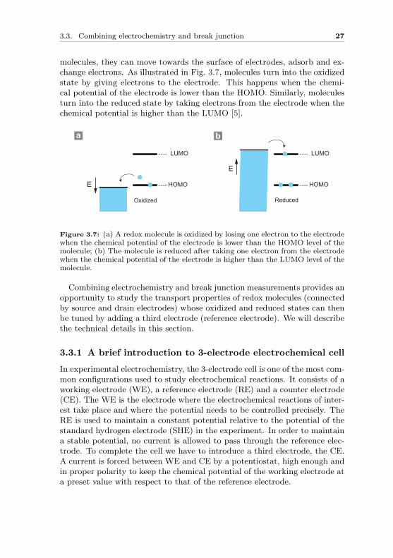
molecules, they can move towards the surface of electrodes, adsorb and ex-change electrons. As illustrated in Fig. 3.7, molecules turn into the oxidizedstate by giving electrons to the electrode. This happens when the chemi-cal potential of the electrode is lower than the HOMO. Similarly, moleculesturn into the reduced state by taking electrons from the electrode when thechemical potential is higher than the LUMO [5].
LUMO
HOMO
LUMO
HOMOE
E
Oxidized Reduced
a b
Figure 3.7: (a) A redox molecule is oxidized by losing one electron to the electrodewhen the chemical potential of the electrode is lower than the HOMO level of themolecule; (b) The molecule is reduced after taking one electron from the electrodewhen the chemical potential of the electrode is higher than the LUMO level of themolecule.
Combining electrochemistry and break junction measurements provides anopportunity to study the transport properties of redox molecules (connectedby source and drain electrodes) whose oxidized and reduced states can thenbe tuned by adding a third electrode (reference electrode). We will describethe technical details in this section.
3.3.1 A brief introduction to 3-electrode electrochemical cell
In experimental electrochemistry, the 3-electrode cell is one of the most com-mon configurations used to study electrochemical reactions. It consists of aworking electrode (WE), a reference electrode (RE) and a counter electrode(CE). The WE is the electrode where the electrochemical reactions of inter-est take place and where the potential needs to be controlled precisely. TheRE is used to maintain a constant potential relative to the potential of thestandard hydrogen electrode (SHE) in the experiment. In order to maintaina stable potential, no current is allowed to pass through the reference elec-trode. To complete the cell we have to introduce a third electrode, the CE.A current is forced between WE and CE by a potentiostat, high enough andin proper polarity to keep the chemical potential of the working electrode ata preset value with respect to that of the reference electrode.
28 MCBJ: Making electrical contacts to single molecules
The 3 electrodes
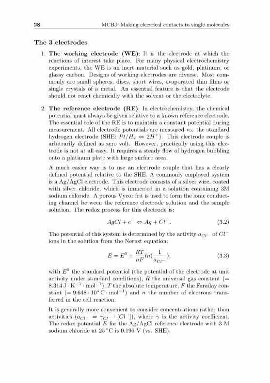
1. The working electrode (WE): It is the electrode at which thereactions of interest take place. For many physical electrochemistryexperiments, the WE is an inert material such as gold, platinum, orglassy carbon. Designs of working electrodes are diverse. Most com-monly are small spheres, discs, short wires, evaporated thin films orsingle crystals of a metal. An essential feature is that the electrodeshould not react chemically with the solvent or the electrolyte.
2. The reference electrode (RE): In electrochemistry, the chemicalpotential must always be given relative to a known reference electrode.The essential role of the RE is to maintain a constant potential duringmeasurement. All electrode potentials are measured vs. the standardhydrogen electrode (SHE: Pt/H2 ⇔ 2H+). This electrode couple isarbitrarily defined as zero volt. However, practically using this elec-trode is not at all easy. It requires a steady flow of hydrogen bubblingonto a platinum plate with large surface area.
A much easier way is to use an electrode couple that has a clearlydefined potential relative to the SHE. A commonly employed systemis a Ag/AgCl electrode. This electrode consists of a silver wire, coatedwith silver chloride, which is immersed in a solution containing 3Msodium chloride. A porous Vycor frit is used to form the ionic conduct-ing channel between the reference electrode solution and the samplesolution. The redox process for this electrode is:
AgCl + e− ⇔ Ag + Cl−. (3.2)
The potential of this system is determined by the activity aCl− of Cl−
ions in the solution from the Nernst equation:
E = E0 +RT
nFln(
1
aCl−), (3.3)
with E0 the standard potential (the potential of the electrode at unitactivity under standard conditions), R the universal gas constant (=8.314 J ·K−1 ·mol−1), T the absolute temperature, F the Faraday con-stant (= 9.648 · 104 C ·mol−1) and n the number of electrons trans-ferred in the cell reaction.
It is generally more convenient to consider concentrations rather thanactivities (aCl− = γCl− · [Cl−]), where γ is the activity coefficient.The redox potential E for the Ag/AgCl reference electrode with 3 Msodium chloride at 25 C is 0.196 V (vs. SHE).
3.3. Combining electrochemistry and break junction 29
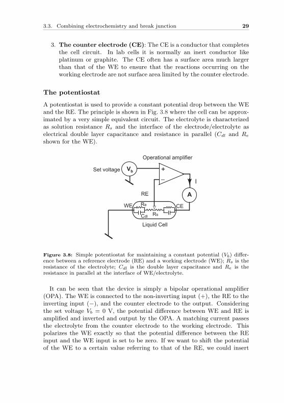
3. The counter electrode (CE): The CE is a conductor that completesthe cell circuit. In lab cells it is normally an inert conductor likeplatinum or graphite. The CE often has a surface area much largerthan that of the WE to ensure that the reactions occurring on theworking electrode are not surface area limited by the counter electrode.
The potentiostat
A potentiostat is used to provide a constant potential drop between the WEand the RE. The principle is shown in Fig. 3.8 where the cell can be approx-imated by a very simple equivalent circuit. The electrolyte is characterizedas solution resistance Rs and the interface of the electrode/electrolyte aselectrical double layer capacitance and resistance in parallel (Cdl and Re
shown for the WE).
+_
Operational amplifier
VbSet voltage
RE
CE
A
WE
Liquid Cell
I
Cdl Rs
Re
Figure 3.8: Simple potentiostat for maintaining a constant potential (Vb) differ-ence between a reference electrode (RE) and a working electrode (WE); Rs is theresistance of the electrolyte; Cdl is the double layer capacitance and Re is theresistance in parallel at the interface of WE/electrolyte.
It can be seen that the device is simply a bipolar operational amplifier(OPA). The WE is connected to the non-inverting input (+), the RE to theinverting input (−), and the counter electrode to the output. Consideringthe set voltage Vb = 0 V, the potential difference between WE and RE isamplified and inverted and output by the OPA. A matching current passesthe electrolyte from the counter electrode to the working electrode. Thispolarizes the WE exactly so that the potential difference between the REinput and the WE input is set to be zero. If we want to shift the potentialof the WE to a certain value referring to that of the RE, we could insert
30 MCBJ: Making electrical contacts to single molecules
a voltage Vb (6= 0) to the non-inverting input (+) of the amplifier. In elec-trochemistry, one usually considers the potential of the RE as zero. Thepotential E at the WE/electrolyte interface therefore equals −Vb.
A high input-impedance operational amplifier is used in order to furtherdiminish the current passing through the reference electrode. And the REinput is commonly protected by an input resistor, which prevents the poten-tial amplifier from being destroyed by static high voltage shocks when theinput is open.
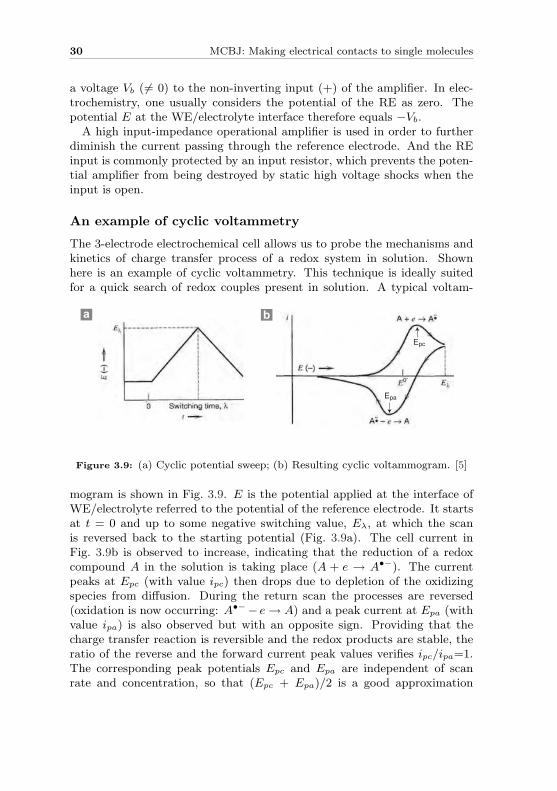
An example of cyclic voltammetry
The 3-electrode electrochemical cell allows us to probe the mechanisms andkinetics of charge transfer process of a redox system in solution. Shownhere is an example of cyclic voltammetry. This technique is ideally suitedfor a quick search of redox couples present in solution. A typical voltam-
a b
Epc
Epa
Figure 3.9: (a) Cyclic potential sweep; (b) Resulting cyclic voltammogram. [5]
mogram is shown in Fig. 3.9. E is the potential applied at the interface ofWE/electrolyte referred to the potential of the reference electrode. It startsat t = 0 and up to some negative switching value, Eλ, at which the scanis reversed back to the starting potential (Fig. 3.9a). The cell current inFig. 3.9b is observed to increase, indicating that the reduction of a redoxcompound A in the solution is taking place (A + e → A•−). The currentpeaks at Epc (with value ipc) then drops due to depletion of the oxidizingspecies from diffusion. During the return scan the processes are reversed(oxidation is now occurring: A•−− e → A) and a peak current at Epa (withvalue ipa) is also observed but with an opposite sign. Providing that thecharge transfer reaction is reversible and the redox products are stable, theratio of the reverse and the forward current peak values verifies ipc/ipa=1.The corresponding peak potentials Epc and Epa are independent of scanrate and concentration, so that (Epc + Epa)/2 is a good approximation
3.3. Combining electrochemistry and break junction 31
of E0′ which is the formal potential for the redox reaction. Furthermore,Ep = Epa −Epc should be close to 59 mV for one electron transfer reactionat all scan rates. These features are very convenient diagnostic tools to testfor the reversibility of a redox process and stability of the reaction products.
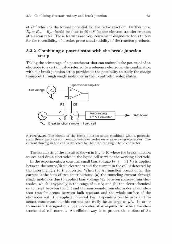
3.3.2 Combining a potentiostat with the break junctionsetup
Taking the advantage of a potentiostat that can maintain the potential of anelectrode to a certain value referred to a reference electrode, the combinationwith our break junction setup provides us the possibility to study the chargetransport through single molecules in their controlled redox states.
VbVb1
+_
AutorangingI to V Converter DAQ board
Operational amplifier
Vb2Set voltage
RE CE
Break junction sample in liquid cell
S D
Figure 3.10: The circuit of the break junction setup combined with a potentio-stat. Break junction source-and-drain electrodes serve as working electrodes. Thecurrent flowing in the cell is detected by the auto-ranging I to V converter.
The schematic of the circuit is shown in Fig. 3.10 where the break junctionsource-and-drain electrodes in the liquid cell serve as the working electrode.
In the experiments, a constant small bias voltage Vb1 (= 0.1 V) is appliedbetween the source/drain electrodes and the current in the cell is detected bythe autoranging I to V converter. When the Au junction breaks open, thiscurrent is the sum of two contributions: (a) the tunneling current throughsingle molecules due to applied bias voltage Vb1 between source/drain elec-trodes, which is typically in the range of ∼ nA; and (b) the electrochemicalcell current between the CE and the source-and-drain electrodes where elec-tron transfer occurs between bulk reactant and the whole surface of theelectrodes with the applied potential Vb2. Depending on the area and re-actant concentration, this current can easily be as large as µA. In orderto measure the signal of single molecules, it is required to reduce the elec-trochemical cell current. An efficient way is to protect the surface of Au
32 MCBJ: Making electrical contacts to single molecules
structures as we will see below.
3.3.3 Sample modification for electrochemical breakjunctions
1.
2.
3.
4.
polyimide
Au
Polyimide photoresist
Spin-coating of optical UV resist
Exposure by using a 10 mm wide mask
10 µm
After development, baking and under-etching
UV
a b
Normal break junction sample
10 µm Au Polyimide
CEBreak junction
CE10 µm
SEM pictures of polyimide covered break junctions
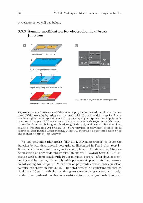
Figure 3.11: (a) Illustration of fabricating a polyimide covered junction with stan-dard UV-lithography by using a stripe mask with 10 µm in width: step 1 - A nor-mal break junction sample after metal deposition; step 2 - Spincoating of polyimidephotoresist; step 3 - UV exposure with a stripe mask with 10 µm in width; step 4- after development, baking and hardening of the polyimide resist, plasma etchingmakes a free-standing Au bridge. (b) SEM pictures of polyimide covered breakjunctions after plasma under-etching. A flat Au structure is fabricated close by asthe counter electrode (see arrows).
We use polyimide photoresist (HD-4104, HD-microsystem) to cover thejunction by standard photolithography as illustrated in Fig. 3.11a: Step 1 -It starts with a normal break junction sample with Au structures; Step 2 -Spincoating of polyimide photoresist (thickness: ∼ 3 µm); Step 3 - UV ex-posure with a stripe mask with 10 µm in width; step 4 - after development,baking and hardening of the polyimide photoresist, plasma etching makes afree-standing Au bridge. SEM pictures of polyimide covered break junctionsamples are shown in Fig. 3.11a. The total area of Au structure exposed toliquid is ∼ 25 µm2, with the remaining Au surface being covered with poly-imide. The hardened polyimide is resistant to polar organic solutions such

3.3. Combining electrochemistry and break junction 33
as dichloromethane and acetonitrile. A counter electrode is also fabricatedon the same sample in this case. Using this structure and configuration, theelectrochemical cell current can be reduced to the sub-nA range and it istherefore now possible to measure the signal of molecular junctions in anelectrochemical cell.

34 MCBJ: Making electrical contacts to single molecules
Chapter 4
Statistical analysis: Seeing signals
of molecular junctions
In our break junction setup we measure the conductance G of a suspendedAu bridge during its breaking process controlled by vertical pushrod move-ment z. The Au junction is repeatedly opened and closed first in pure solventand then in the solution of target molecules. We will see that conductancetraces G(z) show a significant difference between the two situations. Sincesingle curves usually vary from each other, we need a proper statisticalanalysis in order to quantify the conductance value of a particular molecu-lar junction. In this chapter we will introduce a histogram which is basedon a logarithmic representation of G. Combining with conventional linearG-histogram, the molecular signals can easily be identified and deduced.
4.1 Breaking process in pure solvent
We first consider the junction breaking process in a pure solvent (mixture ofTHF/Mesitylene = 1:4 v/v-ratio). Fig. 4.1 shows three typical conductancetraces with several breaking features. The original junction with ∼ 150 nmin width and 200− 300 nm in length has a conductance value well above G0.When the substrate is bent, the Au bridge is stretched and G(z) decreases.When the bridge enters in the range of several strands of Au atom chains, thedecrease evolves in conductance plateaus for G values above the quantumconductance unit G0 (as illustrated in step 1). This process is clearly seen inthe linear plot (Fig. 4.1a). There is a so-called “last plateau”, whose valueis G ≈ G0 (see arrows, step 2). This last plateau corresponds to a singleatom Au contact as explain in the Section 2.2. If the junction is elongatedfurther, it breaks open.
35

36 Statistical analysis: Seeing signals of molecular junctions
open
z
open
z
1
2
3
4
1
2
3
4
G > G0
2
G G0≈
G G0 >
> > G G0
0 20 4010-6
10-5
10-4
10-3
10-2
10-1
100
G/G
0
z (µm)
0 10 20 300
1
2
3
4
5
z (µm)
10 30
a
b
c
G/G
0
Figure 4.1: Three typical opening curves measured in pure solvent and schematicsof breaking process. In break junction experiments, the pushrod is driven at avelocity of vz = 30 µm/s, so that the two Au leads separate at 0.5− 2.0 nm/s. Thecurves are shifted horizontally for clarity: (a) G(z) plot with conductance plateausat multiple values of quantum unit G0; (b) logG(z) presentation with the full viewof breaking process; (c) The breaking features are illustrated in several steps: step1 - quantized conductance plateaus; step 2 - the “last plateau” of single Au atom atG0; step 3 - breaking open of the junction; step 4 - stabilization of the electrodes.
A logG(z) curve gives the full overview of the breaking process betweenseveral G0 and 10−6 G0 (Fig. 4.1b). After the formation of a single atom Aucontact at G0, a sudden decrease of G is evident in the logG(z) curves (step3). This is thought to be caused by a sudden contraction and rearrange-ment of the Au atoms, reshaping the front end of the two Au electrodes.The down-jump typically stops at a value of G ≈ 10−3 G0, when electrontunneling between the electrodes sets in (step 4). The tunneling currentdecays exponentially with gap distance d, whereas on a logG vs lin z plot,it decays linearly.
4.2. Wiring molecules 37
4.2 Wiring molecules
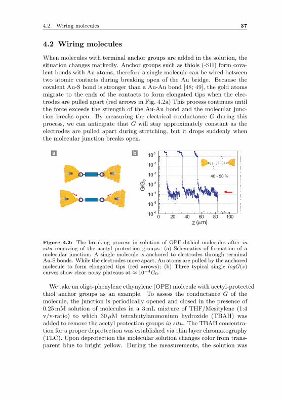
When molecules with terminal anchor groups are added in the solution, thesituation changes markedly. Anchor groups such as thiols (-SH) form cova-lent bonds with Au atoms, therefore a single molecule can be wired betweentwo atomic contacts during breaking open of the Au bridge. Because thecovalent Au-S bond is stronger than a Au-Au bond [48; 49], the gold atomsmigrate to the ends of the contacts to form elongated tips when the elec-trodes are pulled apart (red arrows in Fig. 4.2a) This process continues untilthe force exceeds the strength of the Au-Au bond and the molecular junc-tion breaks open. By measuring the electrical conductance G during thisprocess, we can anticipate that G will stay approximately constant as theelectrodes are pulled apart during stretching, but it drops suddenly whenthe molecular junction breaks open.
0 20 40 60 80 100
G/G
0
(µm)10-6
10-5
10-4
10-3
10-2
10-1
100
40 - 50 %
z
a b
Figure 4.2: The breaking process in solution of OPE-dithiol molecules after insitu removing of the acetyl protection groups: (a) Schematics of formation of amolecular junction: A single molecule is anchored to electrodes through terminalAu-S bonds. While the electrodes move apart, Au atoms are pulled by the anchoredmolecule to form elongated tips (red arrows); (b) Three typical single logG(z)curves show clear noisy plateaus at ≈ 10−4G0.
We take an oligo-phenylene ethynylene (OPE) molecule with acetyl-protectedthiol anchor groups as an example. To assess the conductance G of themolecule, the junction is periodically opened and closed in the presence of0.25mM solution of molecules in a 3mL mixture of THF/Mesitylene (1:4v/v-ratio) to which 30 µM tetrabutylammonium hydroxide (TBAH) wasadded to remove the acetyl protection groups in situ. The TBAH concentra-tion for a proper deprotection was established via thin layer chromatography(TLC). Upon deprotection the molecular solution changes color from trans-parent blue to bright yellow. During the measurements, the solution was
38 Statistical analysis: Seeing signals of molecular junctions
kept under Ar atmosphere to prevent the deprotected bifunctional mole-cules from polymerization via disulfide bond formation. Further details ofdeprotection process are described in Appendix C.2.
Three G(z) curves with the OPE-dithiol molecules are shown in (Fig. 4.2b).Instead of a sudden drop followed by a tunneling slope, as it is observed inthe solvent when the junction opens, clear conductance plateaus appear atG values below G0, typically at G ≈ 10−4 G0 in this case. This is the signa-ture of the formation of a molecular junction. When the molecular junctionbreaks open, there is another sudden drop of conductance value. The chanceof forming molecular junction is not unity, but amounts to a reasonably largefraction of 40− 50% in this case. In the other cases, the electrodes do notcatch molecules. These curves show similar tunneling decay behavior asshown in pure solvent (see Fig. 4.1b).
4.3 Statistical histograms: the linear and logarithmicrepresentations
Since the single conductance curves vary from each other and there are fluc-tuations in the signal, it is important to implement a statistical analysisin order to overcome junction-to-junction variations and quantify conduc-tance value of a particular molecular junction. A conductance histogramwas first proposed and implemented in atomic junctions [6; 50; 51]. It hassubsequently also been used in molecular junctions [52; 40; 25]. Peaks inthe histogram point to preferred junction geometries. Evidence for the for-mation of few-molecules junctions was derived from the observation of aseries of G values appearing at multiples of a fundamental single moleculevalue. But because not all the curves show clear molecular plateaus, dataselection schemes have been applied in order to highlight the molecular sig-nature [53; 54; 55; 56; 57].
We introduce here an alternative histogram based on the logarithm of G.We take all data, and only subtract a background that is adapted to thephysics of the problem.
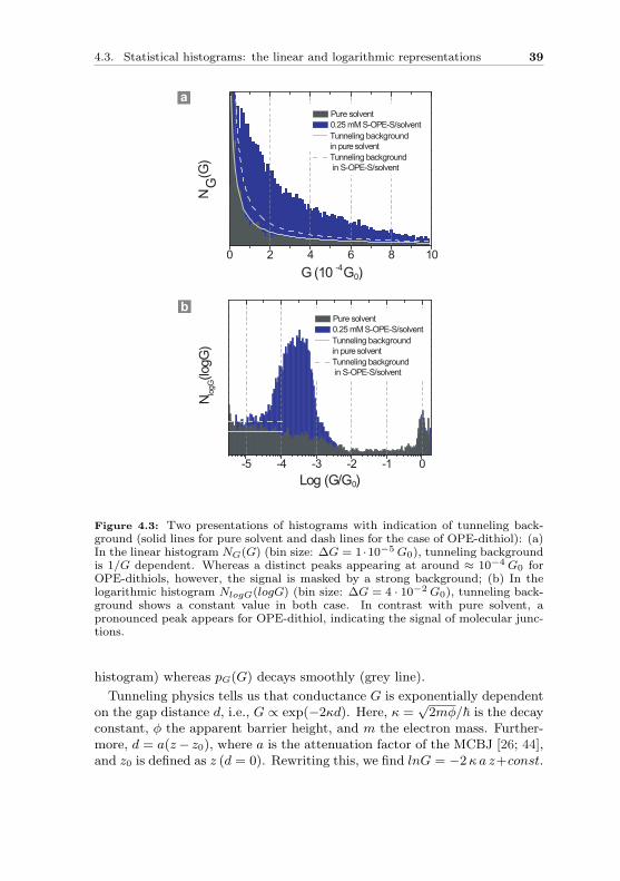
We first take 100 consecutive opening conductance traces G(z) of OPE-dithiol molecules and determine the probability with which a particular G-value is measured, pG(G). This is depicted in the conductance histogramsof Fig. 4.3a (blue histogram). There is a distinct peak appearing at around1 · 10−4 G0, however, the signal is masked by a strong background.
We notice that the background comes from the tunneling decay. Sincethere is ∼ 50% chance that the electrodes do not catch the molecule, theexponential decay of tunneling current must also contribute to the conduc-tance histogram, as already seen in the case of pure solvent Fig. 4.3a (grey
4.3. Statistical histograms: the linear and logarithmic representations 39
-5 -4 -3 -2 -1 0
0.25 mM S-OPE-S/solvent Pure solvent
0 2 4 6 8 10G (10 -4G0)
Tunneling background in S-OPE-S/solvent
Tunneling background in pure solvent
Log (G/G0)
0.25 mM S-OPE-S/solvent Pure solvent
Tunneling background in S-OPE-S/solvent
Tunneling background in pure solvent
N(G
)G
a
b
N logG
(logG
)
Figure 4.3: Two presentations of histograms with indication of tunneling back-ground (solid lines for pure solvent and dash lines for the case of OPE-dithiol): (a)In the linear histogram NG(G) (bin size: ∆G = 1 ·10−5 G0), tunneling backgroundis 1/G dependent. Whereas a distinct peaks appearing at around ≈ 10−4 G0 forOPE-dithiols, however, the signal is masked by a strong background; (b) In thelogarithmic histogram NlogG(logG) (bin size: ∆G = 4 · 10−2 G0), tunneling back-ground shows a constant value in both case. In contrast with pure solvent, apronounced peak appears for OPE-dithiol, indicating the signal of molecular junc-tions.
histogram) whereas pG(G) decays smoothly (grey line).
Tunneling physics tells us that conductance G is exponentially dependenton the gap distance d, i.e., G ∝ exp(−2κd). Here, κ =
√2mφ/~ is the decay
constant, φ the apparent barrier height, and m the electron mass. Further-more, d = a(z− z0), where a is the attenuation factor of the MCBJ [26; 44],and z0 is defined as z (d = 0). Rewriting this, we find lnG = −2 κ a z+const.
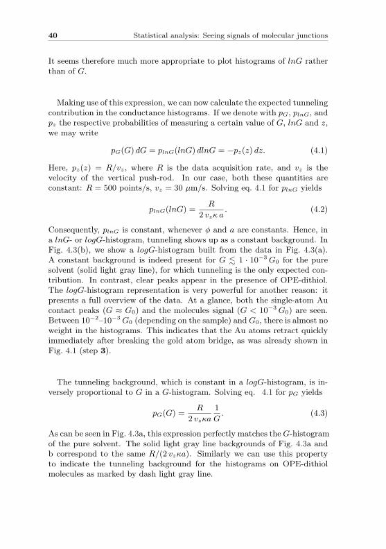
40 Statistical analysis: Seeing signals of molecular junctions
It seems therefore much more appropriate to plot histograms of lnG ratherthan of G.
Making use of this expression, we can now calculate the expected tunnelingcontribution in the conductance histograms. If we denote with pG, plnG, andpz the respective probabilities of measuring a certain value of G, lnG and z,we may write
pG(G) dG = plnG(lnG) dlnG = −pz(z) dz. (4.1)
Here, pz(z) = R/vz, where R is the data acquisition rate, and vz is thevelocity of the vertical push-rod. In our case, both these quantities areconstant: R = 500 points/s, vz = 30 µm/s. Solving eq. 4.1 for plnG yields
plnG(lnG) =R
2 vzκ a. (4.2)
Consequently, plnG is constant, whenever φ and a are constants. Hence, ina lnG- or logG-histogram, tunneling shows up as a constant background. InFig. 4.3(b), we show a logG-histogram built from the data in Fig. 4.3(a).A constant background is indeed present for G . 1 · 10−3 G0 for the puresolvent (solid light gray line), for which tunneling is the only expected con-tribution. In contrast, clear peaks appear in the presence of OPE-dithiol.The logG-histogram representation is very powerful for another reason: itpresents a full overview of the data. At a glance, both the single-atom Aucontact peaks (G ≈ G0) and the molecules signal (G < 10−3 G0) are seen.Between 10−2–10−3 G0 (depending on the sample) and G0, there is almost noweight in the histograms. This indicates that the Au atoms retract quicklyimmediately after breaking the gold atom bridge, as was already shown inFig. 4.1 (step 3).
The tunneling background, which is constant in a logG-histogram, is in-versely proportional to G in a G-histogram. Solving eq. 4.1 for pG yields
pG(G) =R
2 vzκa
1
G. (4.3)
As can be seen in Fig. 4.3a, this expression perfectly matches the G-histogramof the pure solvent. The solid light gray line backgrounds of Fig. 4.3a andb correspond to the same R/(2 vzκa). Similarly we can use this propertyto indicate the tunneling background for the histograms on OPE-dithiolmolecules as marked by dash light gray line.
4.4. Deducing the conductance value of molecular junctions 41
4.4 Deducing the conductance value of molecularjunctions
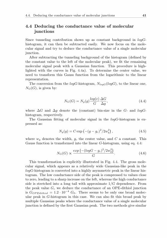
Since tunneling contribution shows up as constant background in logG-histogram, it can then be subtracted easily. We now focus on the mole-cular signal and try to deduce the conductance value of a single molecularjunction.
After subtracting the tunneling background of the histogram (defined bythe constant value to the left of the molecular peak), we fit the remainingmolecular signal peak with a Gaussian function. This procedure is high-lighted with the curves in Fig. 4.4a). To determine the center value, weneed to transform this Gauss function from the logarithmic to the linearrepresentation.
The conversion from the logG-histogram, NlogG(logG), to the linear one,NG(G), is given by:
NG(G) = Ng(g)log(e)
G
∆G
∆g, (4.4)
where ∆G and ∆g denote the (constant) bin-size in the G- and logG-histogram, respectively.
The Gaussian fitting of molecular signal in the logG-histogram is ex-pressed as:
Ng(g) = C exp−(g − gc)
2/2w2g
, (4.5)
where wg denotes the width, gc the center value, and C a constant. ThisGauss function is transformed into the linear G-histogram, using eq. 4.4:
NG(G) ∝exp
−(logG− gc)
2/2w2g
G
. (4.6)
This transformation is explicitly illustrated in Fig. 4.4. The gross mole-cular signal, which appears as a relatively wide Gaussian-like peak in thelogG-histogram is converted into a highly asymmetric peak in the linear his-togram. The low conductance side of the peak is compressed to values closeto zero, leading to a sharp increase on the left, whereas the high conductanceside is stretched into a long tail with approximate 1/G dependence. Fromthe peak value Gc we deduce the conductance of an OPE-dithiol junctionis GOPEdithiol = 1.2 · 10−4 G0. There seems to be only one broad molec-ular peak in G-histogram in this case. We can also fit this broad peak bymultiple Gaussian peaks where the conductance value of a single molecularjunction is defined by the first Gaussian peak. The two methods give similar
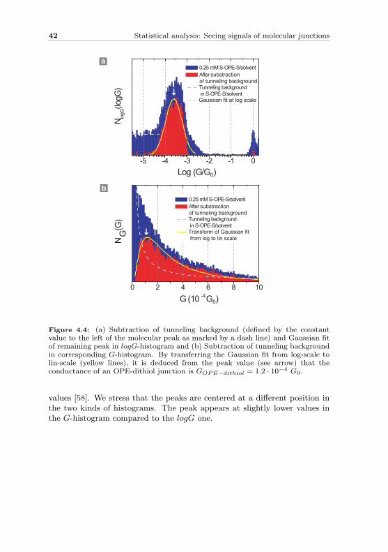
42 Statistical analysis: Seeing signals of molecular junctions
-5 -4 -3 -2 -1 0Log (G/G0)
0.25 mM S-OPE-S/solvent After substraction of tunneling background
0 2 4 6 8 10
G (10 -4G0)
Tunneling background in S-OPE-S/solvent Gaussian fit at log scale
0.25 mM S-OPE-S/solvent After substraction of tunneling background Tunneling background in S-OPE-S/solvent Transform of Gaussian fit from log to lin scale
N(G
)G
a
b
N logG
(logG
)
Figure 4.4: (a) Subtraction of tunneling background (defined by the constantvalue to the left of the molecular peak as marked by a dash line) and Gaussian fitof remaining peak in logG-histogram and (b) Subtraction of tunneling backgroundin corresponding G-histogram. By transferring the Gaussian fit from log-scale tolin-scale (yellow lines), it is deduced from the peak value (see arrow) that theconductance of an OPE-dithiol junction is GOPE−dithiol = 1.2 · 10−4 G0.
values [58]. We stress that the peaks are centered at a different position inthe two kinds of histograms. The peak appears at slightly lower values inthe G-histogram compared to the logG one.
4.5. Sample-to-sample variation 43
4.5 Sample-to-sample variation
After describing the fitting and analysis procedure, we can discuss the sampledependent variances of measurements in the logG-histogram.
0 2 4 6 8 10
G (10 -4G0)
N(G
)G
Sample 1
Sample 2
Sample 3
1.5 x10 -4G0
1.1 x10 -4G0
1.2 x10 -4G0
Log (G/G0)-5 -4 -3 -2 -1 0
Sample 1 Sample 2 Sample 3
a
b
N logG
(logG
)
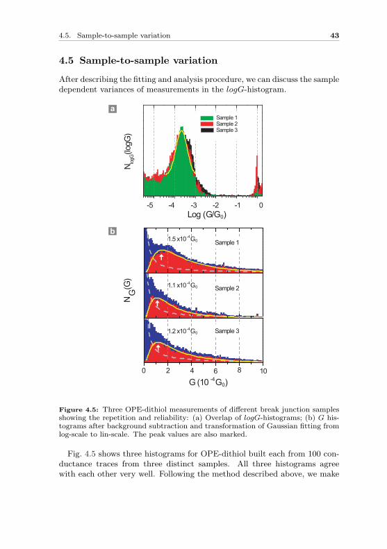
Figure 4.5: Three OPE-dithiol measurements of different break junction samplesshowing the repetition and reliability: (a) Overlap of logG-histograms; (b) G his-tograms after background subtraction and transformation of Gaussian fitting fromlog-scale to lin-scale. The peak values are also marked.
Fig. 4.5 shows three histograms for OPE-dithiol built each from 100 con-ductance traces from three distinct samples. All three histograms agreewith each other very well. Following the method described above, we make
44 Statistical analysis: Seeing signals of molecular junctions
Gaussian fit in the logG histograms as shown in Fig. 4.5a (only the fittingfor the front histogram is shown for clarity) and obtain the peak value gc
and the width w. We then use the transformation between the log- and lin-scale histograms to deduce the conductance values Gc in the linear scale.The values for gc, w and Gc are summarized in Table 4.1.
Samplegc wg Gc
log(G0) log(G0) 10−4 G0
Sample 1 -3.67 0.54 1.5
Sample 2 -3.70 0.70 1.1
Sample 3 -3.60 0.75 1.2
Table 4.1: Values of gc, w obtained from logG-histograms in Fig. 4.5a and Gc fromG-histograms in Fig. 4.5b are quite similar for three different samples.
The transformation gives similar values in G-histograms. By taking the3 conductance value and make standard deviation out of them, we find theconductance value of a OPEdithiol molecular junction which is GOPEdithol =(1.3± 0.2) · 10−4 G0.
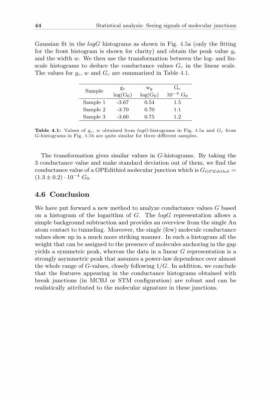
4.6 Conclusion
We have put forward a new method to analyze conductance values G basedon a histogram of the logarithm of G. The logG representation allows asimple background subtraction and provides an overview from the single Auatom contact to tunneling. Moreover, the single (few) molecule conductancevalues show up in a much more striking manner. In such a histogram all theweight that can be assigned to the presence of molecules anchoring in the gapyields a symmetric peak, whereas the data in a linear G representation is astrongly asymmetric peak that assumes a power-law dependence over almostthe whole range of G-values, closely following 1/G. In addition, we concludethat the features appearing in the conductance histograms obtained withbreak junctions (in MCBJ or STM configuration) are robust and can berealistically attributed to the molecular signature in these junctions.
Chapter 5
The role of contacts in molecular
conductance
In order to wire molecules between source and drain electrodes and measuretheir transport properties, it is required to design molecules with anchorgroups. Anchor groups not only ensure a mechanical stabilization of mole-cular junctions, but more importantly, provide at the same time electroniccoupling between a molecule and the contact electrodes. Here we use oligo-phenylene ethynylene (OPE) molecules as model system. In the first sec-tion we compare binding properties of thiol and pyridine by systematicallychanging the linker groups. In the second section, more linker groups suchas amines and different effects of side groups on thiol and amine anchoredOPE molecules are discussed.
5.1 A comparison between thiol and pyridine
To date, thiols are the most widely used anchor groups to Au electrodes.They bind through the formation of Au-S covalent bond. Based on theknowledge of self-assembled monolayers (SAM), many electron donors, suchas pyridines, can also have interactions with the Au surface through weakelectron donor-acceptor bond. We study and compare here the effects ofthiol- and pyridine- anchor groups on molecular conductance.
Fig. 5.1 shows the molecules designed in this work. Linker groups arechanged gradually as marked by dash circles: With the same OPE conju-gated backbone structure, OPE-dithiol serves as a reference molecule (OPESS),then one thiol linker group is replaced by a pyridine nitrogen (OPESN), andfinally we measure a symmetric OPE-bipyridine molecule (OPENN).
45
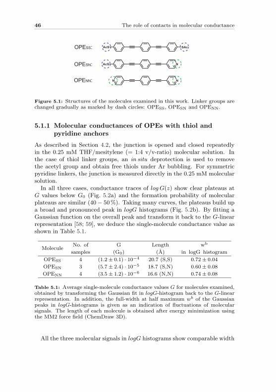
46 The role of contacts in molecular conductance
OPESN:
OPENN:
OPESS: AcS SAc
NAcS
N N
Figure 5.1: Structures of the molecules examined in this work. Linker groups arechanged gradually as marked by dash circles: OPESS, OPESN and OPENN.
5.1.1 Molecular conductances of OPEs with thiol andpyridine anchors
As described in Section 4.2, the junction is opened and closed repeatedlyin the 0.25 mM THF/mesitylene (= 1:4 v/v-ratio) molecular solution. Inthe case of thiol linker groups, an in situ deprotection is used to removethe acetyl group and obtain free thiols under Ar bubbling. For symmetricpyridine linkers, the junction is measured directly in the 0.25 mM molecularsolution.
In all three cases, conductance traces of log G(z) show clear plateaus atG values below G0 (Fig. 5.2a) and the formation probability of molecularplateaus are similar (40− 50%). Taking many curves, the plateaus build upa broad and pronounced peak in logG histograms (Fig. 5.2b). By fitting aGaussian function on the overall peak and transform it back to the G-linearrepresentation [58; 59], we deduce the single-molecule conductance value asshown in Table 5.1.
MoleculeNo. of G Length wb
samples (G0) (A) in logG histogram
OPESS 4 (1.2± 0.1) · 10−4 20.7 (S,S) 0.72± 0.04
OPESN 3 (5.7± 2.4) · 10−5 18.7 (S,N) 0.60± 0.08
OPENN 4 (3.5± 1.2) · 10−6 16.6 (N,N) 0.74± 0.08
Table 5.1: Average single-molecule conductance values G for molecules examined,obtained by transforming the Gaussian fit in logG-histogram back to the G-linearrepresentation. In addition, the full-width at half maximum wb of the Gaussianpeaks in logG-histograms is given as an indication of fluctuations of molecularsignals. The length of each molecule is obtained after energy minimization usingthe MM2 force field (ChemDraw 3D).
All the three molecular signals in logG histograms show comparable width
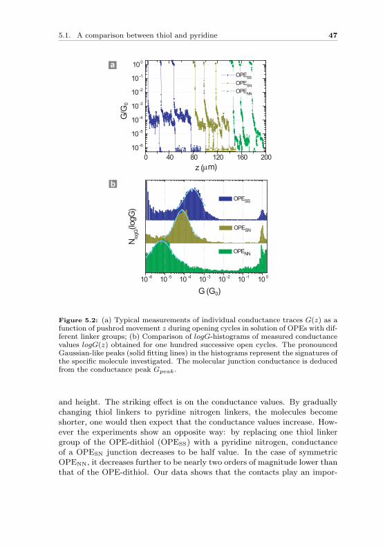
5.1. A comparison between thiol and pyridine 47
SS
SN
N logG
(logG
)
NN
G (G0)10 -6 10 -5 10 -4 10 -3 10 -2 10 -1 10 0
OPE
OPE
OPE
0 40 80 120 160 20010-6
10-5
10-4
10-3
10-2
10-1
100
OPESS OPESN OPENN
G/G
0
z (µm)
a
b
Figure 5.2: (a) Typical measurements of individual conductance traces G(z) as afunction of pushrod movement z during opening cycles in solution of OPEs with dif-ferent linker groups; (b) Comparison of logG-histograms of measured conductancevalues logG(z) obtained for one hundred successive open cycles. The pronouncedGaussian-like peaks (solid fitting lines) in the histograms represent the signatures ofthe specific molecule investigated. The molecular junction conductance is deducedfrom the conductance peak Gpeak.
and height. The striking effect is on the conductance values. By graduallychanging thiol linkers to pyridine nitrogen linkers, the molecules becomeshorter, one would then expect that the conductance values increase. How-ever the experiments show an opposite way: by replacing one thiol linkergroup of the OPE-dithiol (OPESS) with a pyridine nitrogen, conductanceof a OPESN junction decreases to be half value. In the case of symmetricOPENN, it decreases further to be nearly two orders of magnitude lower thanthat of the OPE-dithiol. Our data shows that the contacts play an impor-
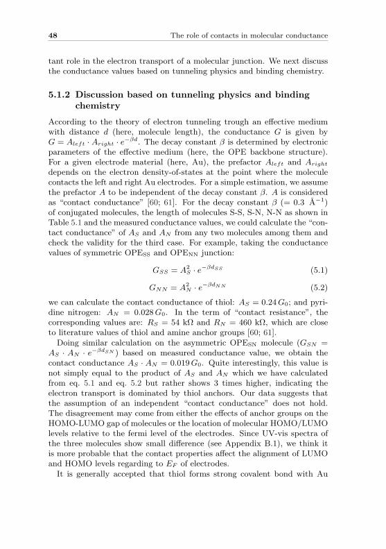
48 The role of contacts in molecular conductance
tant role in the electron transport of a molecular junction. We next discussthe conductance values based on tunneling physics and binding chemistry.
5.1.2 Discussion based on tunneling physics and bindingchemistry
According to the theory of electron tunneling trough an effective mediumwith distance d (here, molecule length), the conductance G is given byG = Aleft ·Aright · e−βd. The decay constant β is determined by electronicparameters of the effective medium (here, the OPE backbone structure).For a given electrode material (here, Au), the prefactor Aleft and Aright
depends on the electron density-of-states at the point where the moleculecontacts the left and right Au electrodes. For a simple estimation, we assumethe prefactor A to be independent of the decay constant β. A is consideredas “contact conductance” [60; 61]. For the decay constant β (= 0.3 A−1)of conjugated molecules, the length of molecules S-S, S-N, N-N as shown inTable 5.1 and the measured conductance values, we could calculate the “con-tact conductance” of AS and AN from any two molecules among them andcheck the validity for the third case. For example, taking the conductancevalues of symmetric OPESS and OPENN junction:
GSS = A2S · e−βdSS (5.1)
GNN = A2N · e−βdNN (5.2)
we can calculate the contact conductance of thiol: AS = 0.24 G0; and pyri-dine nitrogen: AN = 0.028 G0. In the term of “contact resistance”, thecorresponding values are: RS = 54 kΩ and RN = 460 kΩ, which are closeto literature values of thiol and amine anchor groups [60; 61].
Doing similar calculation on the asymmetric OPESN molecule (GSN =AS · AN · e−βdSN ) based on measured conductance value, we obtain thecontact conductance AS · AN = 0.019 G0. Quite interestingly, this value isnot simply equal to the product of AS and AN which we have calculatedfrom eq. 5.1 and eq. 5.2 but rather shows 3 times higher, indicating theelectron transport is dominated by thiol anchors. Our data suggests thatthe assumption of an independent “contact conductance” does not hold.The disagreement may come from either the effects of anchor groups on theHOMO-LUMO gap of molecules or the location of molecular HOMO/LUMOlevels relative to the fermi level of the electrodes. Since UV-vis spectra ofthe three molecules show small difference (see Appendix B.1), we think itis more probable that the contact properties affect the alignment of LUMOand HOMO levels regarding to EF of electrodes.
It is generally accepted that thiol forms strong covalent bond with Au
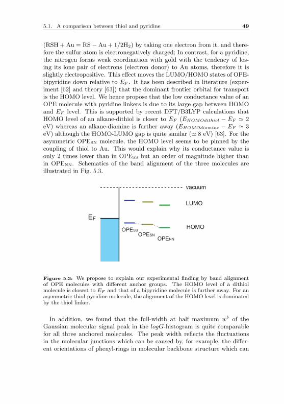
5.1. A comparison between thiol and pyridine 49
(RSH + Au = RS−Au + 1/2H2) by taking one electron from it, and there-fore the sulfur atom is electronegatively charged; In contrast, for a pyridine,the nitrogen forms weak coordination with gold with the tendency of los-ing its lone pair of electrons (electron donor) to Au atoms, therefore it isslightly electropositive. This effect moves the LUMO/HOMO states of OPE-bipyridine down relative to EF . It has been described in literature (exper-iment [62] and theory [63]) that the dominant frontier orbital for transportis the HOMO level. We hence propose that the low conductance value of anOPE molecule with pyridine linkers is due to its large gap between HOMOand EF level. This is supported by recent DFT/B3LYP calculations thatHOMO level of an alkane-dithiol is closer to EF (EHOMOdithiol − EF ' 2eV) whereas an alkane-diamine is further away (EHOMOdiamine − EF ' 3eV) although the HOMO-LUMO gap is quite similar (' 8 eV) [63]. For theasymmetric OPESN molecule, the HOMO level seems to be pinned by thecoupling of thiol to Au. This would explain why its conductance value isonly 2 times lower than in OPESS but an order of magnitude higher thanin OPENN. Schematics of the band alignment of the three molecules areillustrated in Fig. 5.3.
LUMO
EFHOMO
vacuum
OPESNOPENN
OPESS
Figure 5.3: We propose to explain our experimental finding by band alignmentof OPE molecules with different anchor groups. The HOMO level of a dithiolmolecule is closest to EF and that of a bipyridine molecule is further away. For anasymmetric thiol-pyridine molecule, the alignment of the HOMO level is dominatedby the thiol linker.
In addition, we found that the full-width at half maximum wb of theGaussian molecular signal peak in the logG-histogram is quite comparablefor all three anchored molecules. The peak width reflects the fluctuationsin the molecular junctions which can be caused by, for example, the differ-ent orientations of phenyl-rings in molecular backbone structure which can
50 The role of contacts in molecular conductance
disturb the π-system; They can also come from the binding properties, asin the case of Au-S bond, from the switching between different binding sites(hollow, on-top, or bridge site). In the case of pyridine linker, the noise maybe due to the sliding of pyridine atom, possibly also with different bindingsites on the the Au surface.
5.1.3 Concluding comments
In conclusion, we have systematically studied and compared the bindingproperties of thiol and pyridine nitrogen groups. We observed clear mole-cular signals in both symmetric and asymmetric structures. Comparisonof the conductance values for different binding moieties indicates that theband alignment of LUMO and HOMO levels is crucial for the understand-ing of conductance values of formed molecular junctions. To further studythis effect, we propose systematic I-V measurements on these molecules. Inaddition, we have found comparable binding fluctuations for OPE moleculeswith thiol and pyridine linker groups.
5.2 Side group effects
Amine (-NH2) with an electron lone pair on nitrogen atom is another can-didate for electron-donor anchor groups [64]. We also tested its bindingproperties. Molecules with amine anchor groups are shown in Fig. 5.4a withonly OPE backbone (molecule 1a) and to which two methoxy side groupsare attached (molecule 1b). OPE with methoxy anchor groups (molecule2) serves as a control. As comparison, the same structures but with dithiolanchor groups are also shown (molecule 3a and 3b.)
5.2.1 Conductance histograms and discussion
Fig. 5.4b shows typical logG histograms of the molecules. We first take lookat the typical measurement of OPE-diamines (molecule 1a). At first glance,an OPE-diamine molecule does not show clear molecular signal (as markedby dash line). We have measured for 11 samples with different concentrationsand in different solvents (for more histograms see Appendix B.1) but all ofthem show similar results.
As both are nitrogen linkers, why does OPE-bypiridine show clear molec-ular signal but OPE-diamine does not? We propose to interpret our data bythe orbital structure of the molecules. As shown in Fig. 5.5a, the aromaticπ-system of pyridine is the same as that of benzene. The electron lone pairon nitrogen is contained in an sp2-orbital and is orthogonal to the π-system.In contrast, in aromatic amine (aniline in Fig. 5.5b), the sp2-hybridization
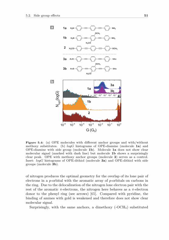
5.2. Side group effects 51
10-6 10-5 10-4 10-3 10-2 10-1 100
N logG(
logG)
G (G0)
H2N NH2
H2N NH2
OCH3
H3CO
1a
1b
S SAc Ac
OCH3
H3CO
SAc SAc
3a
3b
10-5 10-4 10-3 10-2 10-1 100
H3CO OCH32
1a
1b
2
3a
3b
a
b
Figure 5.4: (a) OPE molecules with different anchor groups and with/withoutmethoxy substitutes. (b) logG histograms of OPE-diamine (molecule 1a) andOPE-diamine with side group (molecule 1b). Molecule 1a does not show clearmolecular signal (marked with dash line) but molecule 1b shows a surprisinglyclear peak. OPE with methoxy anchor groups (molecule 2) serves as a control.Inset: logG histograms of OPE-dithiol (molecule 3a) and OPE-dithiol with sidegroups (molecule 3b).
of nitrogen produces the optimal geometry for the overlap of its lone pair ofelectrons in a p-orbital with the aromatic array of p-orbitals on carbons inthe ring. Due to the delocalization of the nitrogen lone electron pair with therest of the aromatic π-electrons, the nitrogen here behaves as a π-electrondonor to the phenyl ring (see arrows) [65]. Compared with pyridine, thebinding of amines with gold is weakened and therefore does not show clearmolecular signal.
Surprisingly, with the same anchors, a dimethoxy (-OCH3) substituted
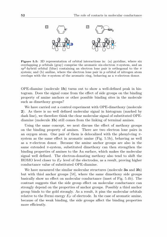
52 The role of contacts in molecular conductance
ba
Figure 5.5: 3D representation of orbital interactions in: (a) pyridine, where sixoverlapping p orbitals (gray) comprise the aromatic six-electron π-system, and ansp2-hybrid orbital (blue) containing an electron lone pair is orthogonal to the πsystem; and (b) aniline, where the electron lone pair in p orbital of nitrogen atomoverlaps with the π-system of the aromatic ring, behaving as a π-electron donor.
OPE-diamine (molecule 1b) turns out to show a well-defined peak in his-togram. Does the signal come from the effect of side groups on the bindingproperty of amine anchors or other possible binding sites in the moleculesuch as dimethoxy groups?
We have carried out a control experiment with OPE-dimethoxy (molecule2). As there is no well defined molecular signal in histogram (marked bydash line), we therefore think the clear molecular signal of substituted OPE-diamine (molecule 1b) still comes from the linking of terminal amines.
Using the same concept, we next discuss the effect of methoxy groupson the binding property of amines. There are two electron lone pairs inan oxygen atom. One pair of them is delocalized with the phenyl-ring π-system as the same effect in aromatic amine (Fig. 5.5b), behaving as wellas a π-electron donor. Because the amine anchor groups are also in thesame extended π-system, substituted dimethoxy can then strengthen thebinding properties of amines to the Au surface, which makes the molecularsignal well defined. The electron-donating methoxy also tend to shift theHOMO level closer to EF level of the electrodes, as a result, proving higherconductance value of substituted OPE-diamine.
We have measured the similar molecular structures (molecule 3a and 3b)but with thiol anchor groups [58], where the same dimethoxy side groupsbasically show no effect on molecular conductance (inset of Fig. 5.4b). Thecontrast suggests that the side group effect on molecular conductance canstrongly depend on the properties of anchor groups. Possibly a thiol anchorgroup binds to the gold strongly. As a result, it pins the molecular orbitalsrelative to the Fermi energy EF of electrode. In the case of aromatic amine,because of the weak binding, the side groups affect the binding propertiesmore efficiently.
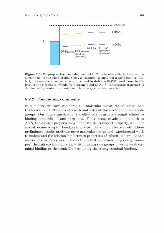
5.2. Side group effects 53
LUMO
EFHOMO
vacuum
OPESS OPESS(dimethoxysubstituted)
OPEdiamine OPEdiamine (dimethoxysubstituted)
Figure 5.6: We propose the band alignment of OPE molecules with thiol and amineanchors under the effect of dimethoxy substituted groups. For a weak bond as Au-NH2, the electron-donating side groups tend to shift the HOMO level closer to EF
level of the electrodes. While for a strong bond as Au-S, the electron transport isdominated by contact property and the side groups have no effect.
5.2.2 Concluding comments
In summary, we have compared the molecular signatures of amine- andthiol-anchored OPE molecules with and without the electron-donating sidegroups. Our data suggests that the effect of side groups strongly relates tobinding properties of anchor groups. For a strong covalent bond such asAu-S, the contact property may dominate the transport property, while fora weak donor-acceptor bond, side groups play a more effective role. Thesepreliminary results motivate more molecular design and experimental workto understand the relationship between properties of substituted groups andanchor groups. Moreover, it shows the potential of controlling charge trans-port through electron-donating/-withdrawing side groups by using weak ter-minal binding or electronically decoupling the strong terminal binding.

54 The role of contacts in molecular conductance
Chapter 6
Molecular junctions based on
aromatic coupling
If individual molecules are to be used as building blocks for electronic de-vices, it will be essential to understand charge transport at the level ofsingle molecules. Most existing experiments rely on the synthesis of func-tional rod-like molecules with chemical linker groups at both ends to pro-vide covalent or donor/acceptor anchoring to the source and drain contacts.This approach has proved very successful, providing quantitative measures ofsingle-molecule conductance, and demonstrating rectification and switchingat the single-molecule level. However, the role of intermolecular interactionshas been overlooked. Here we compare break junction measurements of OPEmolecules with terminal anchor group on both ends and the situations whenthere is only one single anchor group (OPE-monothiol molecules). We willdiscuss the influence of aromatic π-π coupling between adjacent moleculeson the formation and operation of molecular junctions.
6.1 How about taking one anchor group away?
As we have seen in Chapter 5, a single molecule (or a few molecules) with twoterminal anchor groups can be successfully linked in the gap between twoatomic-scale gold contacts to form a molecular junction (Fig. 6.1a). Thiols (-SH) have been widely used as terminal anchor groups. Because the covalentAu-S bond is stronger than a Au-Au bond [48; 66], the Au atoms migrateto the ends of the contacts to form elongated tips when the electrodes arepulled apart (red arrows in Fig. 6.1b). This process continues until the forceexceeds the strength of the Au-Au bond and the molecular junction breaksopen. The electrical conductance of the junction remains approximately
55
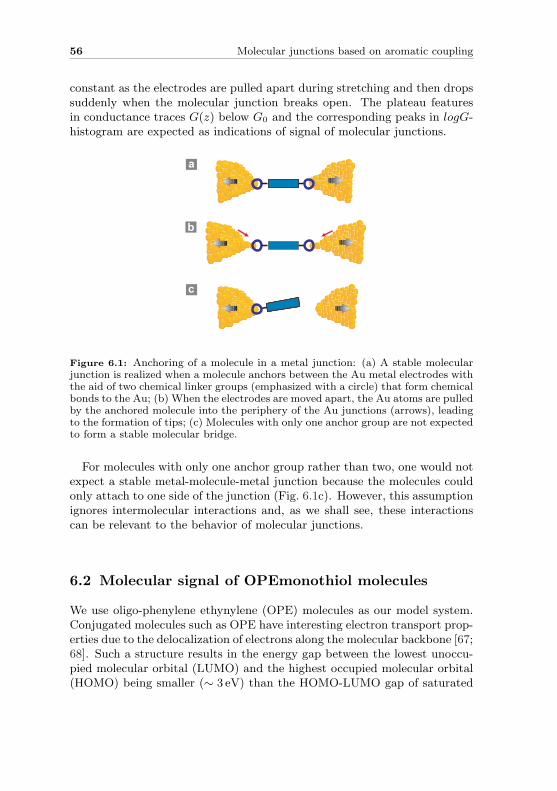
56 Molecular junctions based on aromatic coupling
constant as the electrodes are pulled apart during stretching and then dropssuddenly when the molecular junction breaks open. The plateau featuresin conductance traces G(z) below G0 and the corresponding peaks in logG-histogram are expected as indications of signal of molecular junctions.
a
b
c
Figure 6.1: Anchoring of a molecule in a metal junction: (a) A stable molecularjunction is realized when a molecule anchors between the Au metal electrodes withthe aid of two chemical linker groups (emphasized with a circle) that form chemicalbonds to the Au; (b) When the electrodes are moved apart, the Au atoms are pulledby the anchored molecule into the periphery of the Au junctions (arrows), leadingto the formation of tips; (c) Molecules with only one anchor group are not expectedto form a stable molecular bridge.
For molecules with only one anchor group rather than two, one would notexpect a stable metal-molecule-metal junction because the molecules couldonly attach to one side of the junction (Fig. 6.1c). However, this assumptionignores intermolecular interactions and, as we shall see, these interactionscan be relevant to the behavior of molecular junctions.
6.2 Molecular signal of OPEmonothiol molecules
We use oligo-phenylene ethynylene (OPE) molecules as our model system.Conjugated molecules such as OPE have interesting electron transport prop-erties due to the delocalization of electrons along the molecular backbone [67;68]. Such a structure results in the energy gap between the lowest unoccu-pied molecular orbital (LUMO) and the highest occupied molecular orbital(HOMO) being smaller (∼ 3 eV) than the HOMO-LUMO gap of saturated
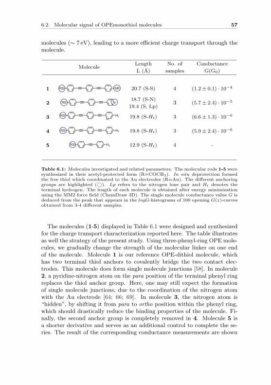
6.2. Molecular signal of OPEmonothiol molecules 57
molecules (∼ 7 eV), leading to a more efficient charge transport through themolecule.
MoleculeLength No. of Conductance
L (A) samples G(G0)
1 RS SR 20.7 (S-S) 4 (1.2± 0.1) · 10−4
2 NRS18.7 (S-N)
3 (5.7± 2.4) · 10−5
19.4 (S, Lp)
3 NRS Ht 19.8 (S-Ht) 3 (6.6± 1.3) · 10−6
4 RS Ht 19.8 (S-Ht) 3 (5.9± 2.4) · 10−6
5 RS Ht 12.9 (S-Ht) 4 -
Table 6.1: Molecules investigated and related parameters. The molecular rods 1-5 weresynthesized in their acetyl-protected form (R=COCH3). In situ deprotection formedthe free thiol which coordinated to the Au electrodes (R=Au). The different anchoringgroups are highlighted (©). Lp refers to the nitrogen lone pair and Ht denotes theterminal hydrogen. The length of each molecule is obtained after energy minimizationusing the MM2 force field (ChemDraw 3D). The single molecule conductance value G isdeduced from the peak that appears in the logG-histograms of 100 opening G(z)-curvesobtained from 3-4 different samples.
The molecules (1-5) displayed in Table 6.1 were designed and synthesizedfor the charge transport characterization reported here. The table illustratesas well the strategy of the present study. Using three-phenyl-ring OPE mole-cules, we gradually change the strength of the molecular linker on one endof the molecule. Molecule 1 is our reference OPE-dithiol molecule, whichhas two terminal thiol anchors to covalently bridge the two contact elec-trodes. This molecule does form single molecule junctions [58]. In molecule2, a pyridine-nitrogen atom on the para position of the terminal phenyl ringreplaces the thiol anchor group. Here, one may still expect the formationof single molecule junctions, due to the coordination of the nitrogen atomwith the Au electrode [64; 66; 69]. In molecule 3, the nitrogen atom is“hidden”, by shifting it from para to ortho position within the phenyl ring,which should drastically reduce the binding properties of the molecule. Fi-nally, the second anchor group is completely removed in 4. Molecule 5 isa shorter derivative and serves as an additional control to complete the se-ries. The result of the corresponding conductance measurements are shown
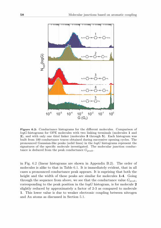
58 Molecular junctions based on aromatic coupling
G (G )0
Au-S S-Au
N-AuAu-S
NAu-S Ht
Au-S Ht
1
2
3
4
5
Au-S Ht
10-6 10-5 10-4 10-3 10-2 10-1 100
NlogG(logG
)
Figure 6.2: Conductance histograms for the different molecules. Comparison oflogG-histograms for OPE molecules with two linking terminals (molecules 1 and2), and with only one thiol linker (molecules 3 through 5). Each histogram wasbuilt from 100 conductance traces obtained during successive opening cycles. Thepronounced Gaussian-like peaks (solid lines) in the logG histograms represent thesignatures of the specific molecule investigated. The molecular junction conduc-tance is deduced from the peak conductance Gpeak.
in Fig. 6.2 (linear histograms are shown in Appendix B.2). The order ofmolecules is alike to that in Table 6.1. It is immediately evident, that in allcases a pronounced conductance peak appears. It is suprising that both theheight and the width of these peaks are similar for molecules 1-4. Goingthrough the sequence from above, we see that the conductance value Gpeak,corresponding to the peak position in the logG histogram, is for molecule 2slightly reduced by approximately a factor of 2-3 as compared to molecule1. This lower value is due to weaker electronic coupling between nitrogenand Au atoms as discussed in Section 5.1.
6.3. The interpretation: π-π stacking 59
Whereas we expect a peak in logG histogram for molecule 2, a similarpeak of equal magnitude for molecule 3 comes as a surprise. Because thenitrogen atom of the pyridine structure is in molecule 3 “hidden”, it mayprovide, if at all, a much less probable binding site to the electrode. Contraryto this, the identical magnitude and width of the peak in logG histogramssuggest that also molecule 3 binds in the junction with a similar probabil-ity as molecules 1 and 2. Hence, the observed strong binding must haveanother origin. This is supported further by the measurements for mole-cule 4. Although the anchor group at one end is now removed, we obtainvery similar results for 3 and 4. Why does a molecular junction form, evenwith molecular rods having only a single linker group on one side of the rod?
6.3 The interpretation: π-π stacking
We think that the connection between the electrodes is made possible by π-πstacking interaction between a pair of molecules [70; 71; 72]. If one moleculeis anchored via its thiol linker group on e.g. the left electrode, another onebound to the right electrode can complete the mechanical assembly of thejunction via π-π coupling through the phenyl rings. This interpretation issupported by the shift of Gpeak to lower values by more than an order ofmagnitude. In this picture, a reduced G value is expected because the pairof molecules will be longer than a single dithiol molecule anchored betweenAu electrodes. We observe that the junctions form with a similar probabil-ity, whether for dithiolated compounds or monothiolated compounds. Thismight a priori appear surprising since the molecular junctions formed bymonothiolated compounds will be composed by two molecules and mighttherefore occur less frequently. This is however not the case since we donot have a diffusion-limited experimental situation. After immersion in themolecular solution, the Au bridge will be covered with a monolayer of mole-cules on its whole surface. Upon breaking the Au bridge open, there willbe a high local concentration of molecules available for the formation of amolecular junction. While the kinetics of junction formation will dependon whether we have dithiolated or monothiolated compounds, the typicaltime constants will be orders of magnitude faster than what our experimen-tal setup can resolve (typically 5 ms). We therefore do not expect to see adifference between both situations.
Since the strength of π-π stacking depends strongly on the conjugationextent of the system and the overlap between adjacent compounds, onestraightforward control experiment, without modifying largely the electronicstructure of the molecules, is to investigate an OPE compound with only
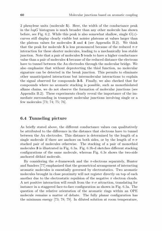
60 Molecular junctions based on aromatic coupling
2 phenylene units (molecule 5). Here, the width of the conductance peakin the logG histogram is much broader than any other molecule has shownbefore, see Fig. 6.2. While this peak is also somewhat shallow, single G(z)-curves still display clearly visible but noisier plateaus at values larger thanthe plateau values for molecules 3 and 4 (see Appendix B.2). We thinkthat the peak for molecule 5 is less pronounced because of the reduced π-πinteraction for these shorter molecules, leading to a mechanically less stablejunction. Note that a pair of molecules 5 tends to have a higher conductancevalue than a pair of molecules 4 because of the reduced distance the electronshave to tunnel between the Au electrodes through the molecular bridge. Wealso emphasize that without deprotecting the thiol function, no molecularsignature can be detected in the break junction. This permits to eliminateother unanticipated interactions but intermolecular interactions to explainthe signal observed for compounds 3-5. Finally, we also checked that forcompounds where no aromatic stacking is possible, such as monothiolatedalkane chains, we do not observe the formation of molecular junctions (seeAppendix B.2). These experiments clearly reveal the importance of the im-mediate surrounding in transport molecular junctions involving single or afew molecules [73; 74; 75; 76].
6.4 Tunneling picture
As briefly stated above, the different conductance values can qualitativelybe attributed to the difference in the distance that electrons have to tunnelbetween the Au electrodes. This distance is determined by the length of asingle molecule if there are anchors on both sides, or by the length of π-πstacked pair of molecules otherwise. The stacking of a pair of monothiolmolecules 3 is illustrated in Fig. 6.3a. Fig. 6.3b-d sketches different stackingconfigurations of the same molecule, whereas Fig. 6.3e shows the two-sideanchored dithiol molecule.
By considering the σ-framework and the π-electrons separately, Hunterand Sanders [77] emphasized that the geometrical arrangement of interactingaromatic molecules is essentially governed by electrostatics. Two aromaticmolecules brought in close proximity will not register directly on top of eachanother due to the electrostatic repulsion of the negative π electron clouds.A net positive interaction will result from the π-σ attraction, translating forinstance in a staggered face-to-face configuration as shown in Fig. 6.3a. Thequestion of the relative orientation of the aromatic rings within an OPEmolecule remains a matter of debate. The fully planar configuration hasthe minimum energy [73; 78; 79]. In diluted solution at room temperature,
6.4. Tunneling picture 61
29.1 Å
22.1 Å
36.0 Å
20.7 Å
a
b
c
d
e
Figure 6.3: Illustration of possible stacking configurations: (a) Staggered π-πstacking configuration of a pair of OPE-monothiol molecules within which the aro-matic rings are shifted by half of the ring length; (b)-(e) Simplified representationof different configurations of OPE molecules between the electrodes. A rectangleindicates a phenyl ring: (b) The configuration anticipated as the most probableone; (c,d) Less probable configurations due to steric hindrance (c) and reduced con-jugation and overlap (d); (e) A single OPE-dithiol molecule between electrodes. Alldistances are taken between the sulfur atoms on both sides and were estimated af-ter minimizing the energy of the compound via a molecular mechanics calculationusing the MM2 force field (ChemDraw 3D).
experiments and calculations suggest however that the aromatic rings ofOPE molecules are able to explore different orientations [78; 80]. This iscertainly true at low concentration. At higher concentrations, where the π-π interaction induces aggregation, coplanar stacking appears favored [79; 81;82]. This is also the case in crystals of similar aromatic compounds [83; 84].In our case, the molecules self-assemble at the surface of the Au electrodes,
62 Molecular junctions based on aromatic coupling
leading to a high local concentration. We therefore expect the molecules toform coplanar stacks as illustrated in Fig. 6.3a. Fig. 6.3b-d depict possiblestacking configurations. We think that Fig. 6.3a,b represents the actualstacking configuration of a pair of molecules 4. Structures 4c and 4d areseen as less probable because of steric hindrance and because of the weakerπ-π interaction due to the reduced overlap between the molecules.
In a simple tunneling picture where electrons tunnel trough an effectivemedium over a distance d, the conductance G can be written as G = A·e−βd.The decay constant β is determined by the electronic parameters of the ef-fective medium (here, the molecules). For a given electrode material (here,Au), the pre-factor A depends on the electron density-of-states at the pointwhere the molecule contacts the Au electrode. Because this is determinedby thiol anchors both in single molecule and stacked pair of molecules, thisfactor can be taken as a constant. Note that in this tunneling picture, thesymmetric and constant peak widths in the logG histograms (Fig. 6.2) reflectthe fact that the conductance fluctuations mainly arise due to variations inthe exponent of the conductance. The conductance fluctuations can there-fore be attributed to variations of the effective tunneling distance d and thedecay constant β as generated by local changes in the geometrical arrange-ment of the molecular junction. Experimental and theoretical evidence havealready been provided for a strong through-space conjugation between πsystems that were held together via carbon linkers [85]. For the followingestimate we will use a typical average decay constant of 0.3 A−1 for the OPEderivatives as obtained from electron transfer rates in donor-bridge-acceptorsystems [86; 87; 88] and theory [89; 90]. The distances between the twosulfur atoms are 20.7 A for the single OPE-dithiol molecule (Fig. 6.3e) and29.1 A for a pair of OPE-monothiols (Fig. 6.3b). The longer tunneling dis-tance between electrodes for a stacking junction leads to a 12 times lowerconductance. This is in reasonable agreement with the experiment whichshows a 20-fold difference.
6.5 Conclusion
In conclusion, we have demonstrated that intermolecular π-π stacking in-teraction between monothiol molecules composed of alternating phenyleneand ethynylene units is strong enough to induce the formation of molecularjunctions. The yield is similar to that of dithiol molecules with a molecularsignature reaching the same degree of quality as judged from the statis-tical variation of single junction conductance values. This is a significantfinding for molecular electronics. Intermolecular aromatic stacking plays a
6.5. Conclusion 63
determinant role in stabilizing nano-objects. The importance of π-π overlaphas long been recognized in thin-film organic electronics, molecular mechan-ics, and especially in biomolecular and supramolecular chemistry. We showhere that π-π stacking can also be used as the dominant guiding force forthe formation of molecular bridges in few molecules electronic junctions.These experimental findings provide a strong ground for the design of fu-ture electro-mechanical and sensing devices operating at the single moleculelevel.

64 Molecular junctions based on aromatic coupling
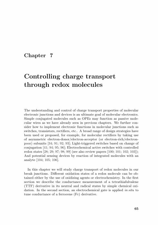
Chapter 7
Controlling charge transport
through redox molecules
The understanding and control of charge transport properties of molecularelectronic junctions and devices is an ultimate goal of molecular electronics.Simple conjugated molecules such as OPEs may function as passive mole-cular wires as we have already seen in previous chapters. We further con-sider how to implement electronic functions in molecular junctions such asswitches, transistors, rectifiers, etc.. A broad range of design strategies havebeen used or proposed, for example, for molecular rectifiers by taking useof asymmetric electron-donor/electron-acceptor (or electron-rich/electron-poor) subunits [34; 91; 92; 93]; Light-triggered switches based on change ofconjugation [41; 94; 95; 96]; Electrochemical active switches with controlledredox states [28; 29; 97; 98; 99] (see also review papers [100; 101; 102; 103]);And potential sensing devices by reaction of integrated molecules with ananalyte [104; 105; 106].
In this chapter we will study charge transport of redox molecules in ourbreak junctions. Different oxidation states of a redox molecule can be ob-tained either by the use of oxidizing agents or electrochemistry. In the firstsection we describe the conductance measurement of a tetrathiafulvalene(TTF) derivative in its neutral and radical states by simple chemical oxi-dation. In the second section, an electrochemical gate is applied in situ totune conductance of a ferrocene (Fc) derivative.
65
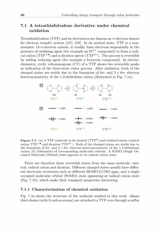
66 Controlling charge transport through redox molecules
7.1 A tetrathiafulvalene derivative under chemicaloxidation
Tetrathiafulvalene (TTF) and its derivatives are famous as π-electron donorsfor electron transfer system [107; 108]. In its neutral state, TTF is a non-aromatic 14-π-electron system; it readily loses electrons sequentially in thepresence of oxidizing agent (for example an Fe3+ compound) to form a radi-cal cation (TTF+•) and a dication specie (TTF2+). The process is reversibleby adding reducing agent (for example a ferrocene compound). In electro-chemistry, cyclic voltammogram (CV) of a TTF shows two reversible peaksas indication of the three-state redox process. After oxidation, both of thecharged states are stable due to the formation of 6π- and 2 × 6π- electronheteroaromaticity of the 1,3-dithiolium cation (illustrated in Fig. 7.1a).
LUMO
HOMO
S
S
S
S
S
S
S
S
S
S
S
S- e
+ e
- e
+ e
6π 6π 6π
LUMO
HOMO
LUMO
HOMOSOMO
TF TTF + TTF 2 +T
TF TTF + TTF 2 +T 0
0
14π
a
b
Figure 7.1: (a) A TTF molecule in its neutral (TTF0) and oxidized states (radical
cation TTF+• and dication TTF2+). Both of the charged states are stable due tothe formation of 6π- and 2 × 6π- electron heteroaromaticity of the 1,3-dithioliumcation; (b) Schematics of corresponding molecular orbitals. A SOMO (Single Oc-cupied Molecular Orbital) state appears at its radical cation state.
There are therefore three reversible states from the same molecule: neu-tral, radical cation and dication. Different charged states usually have differ-ent electronic structures such as different HOMO-LUMO gaps, and a singleoccupied molecular orbital (SOMO) state appearing at radical cation state(Fig. 7.1b), which make their transport properties interesting.
7.1.1 Characterization of chemical oxidation
Fig. 7.2a shows the structure of the molecule studied in this work: alkanethiol chains (with 3 carbon atoms) are attached to TTF core through a sulfur
7.1. A tetrathiafulvalene derivative under chemical oxidation 67
atom. There are two isomers with 1:1 ratio according to different bindingpositions. The reversibility of the redox states can be characterized by CVand photoelectrochemistry (see Appendix B.3).
300 400 500 600 700 800 9000.0
0.2
0.4
0.6
+ in neatral state in TTF
Abso
rptio
n
Wavelength (nm)
S
S
S
SHS S
SHS
TTF alkanedithiol studied in this work
by 1:1 NOBF4
TTF alkanedithiol0 TTF
a
b
Figure 7.2: (a) Structure of TTF derivative studied in this work. Alkane thiolchains (with 3 carbon atoms) are attached to TTF core through a sulfur atom.There are two isomers with 1:1 ratio according to different binding positions (sul-fur atom on the right side binds either on up or down carbon atom); (b) UV-visspectrum of the neutral TTF derivative in dichloromethane (DCM) and the samesolution after adding in 1:1 oxidizing agent NOBF4. Neutral TTF derivative ab-sorbs around 320 nm, while two new absorption bands appear (peaks at 450 nmand 720 nm indicated by arrows) for the radical cation state TTF+•.
It is known that an Fe3+Cl−3 compound is an ideal oxidizing agent for TTFcore structure [109], but we can not use it to oxidize our TTF alkanedithiolhere because it coordinates immediately with free thiols and precipitates asgreen powders. This effect limits our choices of oxidizing agents to be non-metals. Finally we find out that nitrosonium tetrafluoroborate (NOBF4)can oxidize the TTF derivative to the TTF+• state, and at the same time,does not react with the free thiols. The reaction can be characterized clearlyin UV-vis spectrum (Fig. 7.2b). Neutral TTF derivative absorbs around 320nm, while two new absorption bands appear at 450 nm and 720 nm for theradical cation state TTF+• [110; 109]. In the meantime, the color of thesolution turns from yellow to green.
However, the oxidized state turns out to be unstable in air. The two-band absorption of the TTF+• decays gradually upon time and even more
68 Controlling charge transport through redox molecules
dramatically with adding in more NOBF4. This may due to the change ofchemical environment after decomposition of NOBF4. The NOBF4 is verysensitive to water or even moist air and can decomposes to nitrous acid(HNO2), which may then lead to the decomposition of TTF structure. It istherefore important to use dry solvent and keep the atmosphere under Ar.
7.1.2 Molecular conductances of the neutral and radicalcation states
We first try to immobilize the TTF-alkanedithiol in break junctions. Typicalconductance traces G(z) and logG histogram of 0.06 mM neutral TTF deriv-ative in dichloromethane are shown in Fig. 7.3a and b. Molecular plateaustend to appear between 1 ·10−4 and 1 ·10−5 G0 but with low yield (≤ 20%).The histogram built from 100 consecutive opening curves therefore does notshow a clear Gaussian peak, but rather in a shape of slope. The molecularsignal of the TTF derivative is not as well defined as compared with typicalOPE families that we have seen in previous chapters or octanedithiol thatwe have measured before (both with plateaus yield of 40− 50%). More testswith higher concentration (0.6 mM ) in mesitylene solvent have also beencarried out and the results (see Appendix B.3) are quite similar as in thecase of DCM.
Nevertheless we tested the radical cation state of the TTF alkanedithiolin break junctions by using chemical oxidation. A concentrated TTF alka-nedithiol/DCM solution is degassed with bubbling of Ar for 10 min, then a1:1 ratio of NOBF4 is added. A certain amount of the solution of oxidizedmolecules which corresponds to the final 0.06 mM concentration is carefullytransferred into the liquid cell which contains pure degassed DCM and thereis constant Ar bubbling during the measurement.
The typical conductance traces and logG histogram of TTF+• are shownin Fig. 7.3c and d, where molecular signals are better visible. We observedthat in some cases there is a strong tunneling decay background in singlelogG(z) curves (guided by gray dash lines). This feature leads to the largeconstant background in histogram (guided by gray dash lines) and a smallpeak showing up at 1 · 10−4 G0 as the indication of molecular signal.
7.1.3 Discussion
Based on our measurements, the neutral TTF alkanedithiol does not exhibitclear molecular signal (i.e. peaks in logG histogram). There can be severalreasons: first of all, it is possible that the thoil-linking signal is below ourmeasurement resolution (the resolution can reache 1 · 10−6 G0 in mesityleneas shown in Appendix B.3). Secondly, there can be other binding possibilities
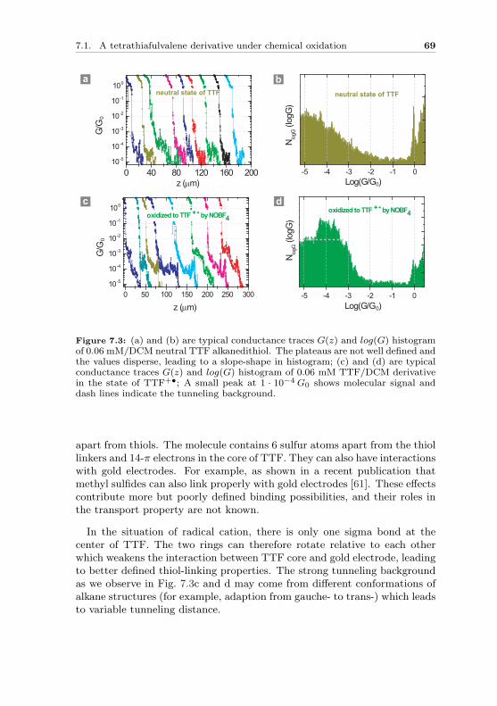
7.1. A tetrathiafulvalene derivative under chemical oxidation 69
-5 -4 -3 -2 -1 0
N logG
(log
G)
Log(G/G0)
Log(G/G0)0 50 100 150 200 250 300
10-5
10-4
10-3
10-2
10-1
100
oxidized to TTF + by NOBF4
G/G
0
z (µm)
0 40 80 120 160 20010-5
10-4
10-3
10-2
10-1
100
G/G
0
z (µm)
neutral state of TTF
N logG
(log
G)
oxidized to TTF + by NOBF4
neutral state of TTF
-5 -4 -3 -2 -1 0
a b
c d
Figure 7.3: (a) and (b) are typical conductance traces G(z) and log(G) histogramof 0.06 mM/DCM neutral TTF alkanedithiol. The plateaus are not well defined andthe values disperse, leading to a slope-shape in histogram; (c) and (d) are typicalconductance traces G(z) and log(G) histogram of 0.06 mM TTF/DCM derivativein the state of TTF+•; A small peak at 1 · 10−4 G0 shows molecular signal anddash lines indicate the tunneling background.
apart from thiols. The molecule contains 6 sulfur atoms apart from the thiollinkers and 14-π electrons in the core of TTF. They can also have interactionswith gold electrodes. For example, as shown in a recent publication thatmethyl sulfides can also link properly with gold electrodes [61]. These effectscontribute more but poorly defined binding possibilities, and their roles inthe transport property are not known.
In the situation of radical cation, there is only one sigma bond at thecenter of TTF. The two rings can therefore rotate relative to each otherwhich weakens the interaction between TTF core and gold electrode, leadingto better defined thiol-linking properties. The strong tunneling backgroundas we observe in Fig. 7.3c and d may come from different conformations ofalkane structures (for example, adaption from gauche- to trans-) which leadsto variable tunneling distance.
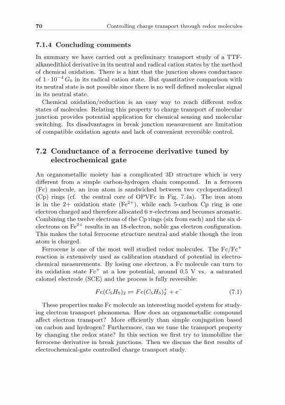
70 Controlling charge transport through redox molecules
7.1.4 Concluding comments
In summary we have carried out a preliminary transport study of a TTF-alkanedithiol derivative in its neutral and radical cation states by the methodof chemical oxidation. There is a hint that the junction shows conductanceof 1 · 10−4 G0 in its radical cation state. But quantitative comparison withits neutral state is not possible since there is no well defined molecular signalin its neutral state.
Chemical oxidation/reduction is an easy way to reach different redoxstates of molecules. Relating this property to charge transport of molecularjunction provides potential application for chemical sensing and molecularswitching. Its disadvantages in break junction measurement are limitationof compatible oxidation agents and lack of convenient reversible control.
7.2 Conductance of a ferrocene derivative tuned byelectrochemical gate
An organometallic moiety has a complicated 3D structure which is verydifferent from a simple carbon-hydrogen chain compound. In a ferrocen(Fc) molecule, an iron atom is sandwiched between two cyclopentadienyl(Cp) rings (cf. the central core of OPVFc in Fig. 7.4a). The iron atomis in the 2+ oxidation state (Fe2+), while each 5-carbon Cp ring is oneelectron charged and therefore allocated 6 π-electrons and becomes aromatic.Combining the twelve electrons of the Cp rings (six from each) and the six d-electrons on Fe2+ results in an 18-electron, noble gas electron configuration.This makes the total ferrocene structure neutral and stable though the ironatom is charged.
Ferrocene is one of the most well studied redox molecules. The Fc/Fc+
reaction is extensively used as calibration standard of potential in electro-chemical measurements. By losing one electron, a Fc molecule can turn toits oxidation state Fc+ at a low potential, around 0.5 V vs. a saturatedcalomel electrode (SCE) and the process is fully reversible:
Fe(C5H5)2 Fe(C5H5)+2 + e− (7.1)
These properties make Fc molecule an interesting model system for study-ing electron transport phenomena. How does an organometallic compoundaffect electron transport? More efficiently than simple conjugation basedon carbon and hydrogen? Furthermore, can we tune the transport propertyby changing the redox state? In this section we first try to immobilize theferrocene derivative in break junctions. Then we discuss the first results ofelectrochemical-gate controlled charge transport study.
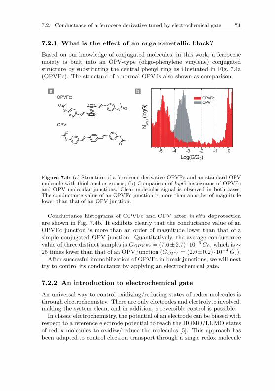
7.2. Conductance of a ferrocene derivative tuned by electrochemical gate 71
7.2.1 What is the effect of an organometallic block?
Based on our knowledge of conjugated molecules, in this work, a ferrocenemoiety is built into an OPV-type (oligo-phenylene vinylene) conjugatedstructure by substituting the central phenyl ring as illustrated in Fig. 7.4a(OPVFc). The structure of a normal OPV is also shown as comparison.
OPVFc:
Fe S OSO
SSO
O
-5 -4 -3 -2 -1 0N log
G (lo
gG)
Log(G/G0)
OPV OPVFc
OPV:
a b
Figure 7.4: (a) Structure of a ferrocene derivative OPVFc and an standard OPVmolecule with thiol anchor groups; (b) Comparison of logG histograms of OPVFcand OPV molecular junctions. Clear molecular signal is observed in both cases.The conductance value of an OPVFc junction is more than an order of magnitudelower than that of an OPV junction.
Conductance histograms of OPVFc and OPV after in situ deprotectionare shown in Fig. 7.4b. It exhibits clearly that the conductance value of anOPVFc junction is more than an order of magnitude lower than that of asimple conjugated OPV junction. Quantitatively, the average conductancevalue of three distinct samples is GOPV Fc = (7.6±2.7) ·10−6 G0, which is ∼25 times lower than that of an OPV junction (GOPV = (2.0±0.2) ·10−4 G0).
After successful immobilization of OPVFc in break junctions, we will nexttry to control its conductance by applying an electrochemical gate.
7.2.2 An introduction to electrochemical gate
An universal way to control oxidizing/reducing states of redox molecules isthrough electrochemistry. There are only electrodes and electrolyte involved,making the system clean, and in addition, a reversible control is possible.
In classic electrochemistry, the potential of an electrode can be biased withrespect to a reference electrode potential to reach the HOMO/LUMO statesof redox molecules to oxidize/reduce the molecules [5]. This approach hasbeen adapted to control electron transport through a single redox molecule
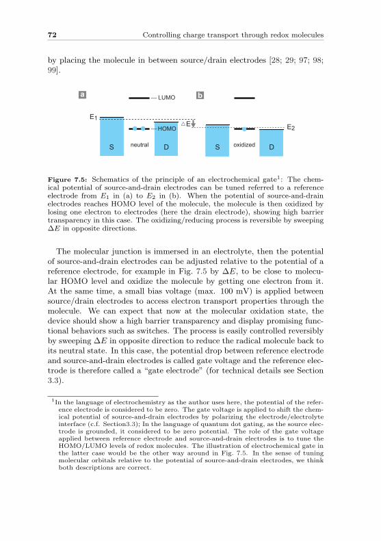
72 Controlling charge transport through redox molecules
by placing the molecule in between source/drain electrodes [28; 29; 97; 98;99].
E1E2
a b
Figure 7.5: Schematics of the principle of an electrochemical gate1: The chem-ical potential of source-and-drain electrodes can be tuned referred to a referenceelectrode from E1 in (a) to E2 in (b). When the potential of source-and-drainelectrodes reaches HOMO level of the molecule, the molecule is then oxidized bylosing one electron to electrodes (here the drain electrode), showing high barriertransparency in this case. The oxidizing/reducing process is reversible by sweeping∆E in opposite directions.
The molecular junction is immersed in an electrolyte, then the potentialof source-and-drain electrodes can be adjusted relative to the potential of areference electrode, for example in Fig. 7.5 by ∆E, to be close to molecu-lar HOMO level and oxidize the molecule by getting one electron from it.At the same time, a small bias voltage (max. 100 mV) is applied betweensource/drain electrodes to access electron transport properties through themolecule. We can expect that now at the molecular oxidation state, thedevice should show a high barrier transparency and display promising func-tional behaviors such as switches. The process is easily controlled reversiblyby sweeping ∆E in opposite direction to reduce the radical molecule back toits neutral state. In this case, the potential drop between reference electrodeand source-and-drain electrodes is called gate voltage and the reference elec-trode is therefore called a “gate electrode” (for technical details see Section3.3).
1In the language of electrochemistry as the author uses here, the potential of the refer-ence electrode is considered to be zero. The gate voltage is applied to shift the chem-ical potential of source-and-drain electrodes by polarizing the electrode/electrolyteinterface (c.f. Section3.3); In the language of quantum dot gating, as the source elec-trode is grounded, it considered to be zero potential. The role of the gate voltageapplied between reference electrode and source-and-drain electrodes is to tune theHOMO/LUMO levels of redox molecules. The illustration of electrochemical gate inthe latter case would be the other way around in Fig. 7.5. In the sense of tuningmolecular orbitals relative to the potential of source-and-drain electrodes, we thinkboth descriptions are correct.
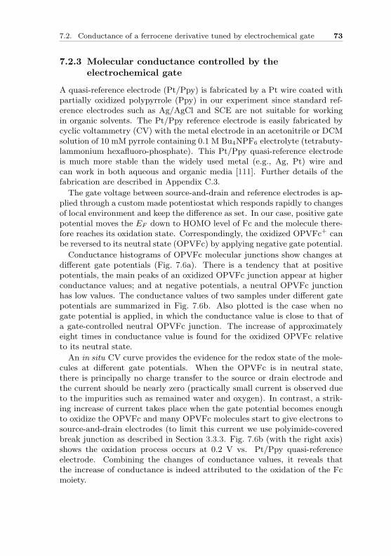
7.2. Conductance of a ferrocene derivative tuned by electrochemical gate 73
7.2.3 Molecular conductance controlled by theelectrochemical gate
A quasi-reference electrode (Pt/Ppy) is fabricated by a Pt wire coated withpartially oxidized polypyrrole (Ppy) in our experiment since standard ref-erence electrodes such as Ag/AgCl and SCE are not suitable for workingin organic solvents. The Pt/Ppy reference electrode is easily fabricated bycyclic voltammetry (CV) with the metal electrode in an acetonitrile or DCMsolution of 10 mM pyrrole containing 0.1 M Bu4NPF6 electrolyte (tetrabuty-lammonium hexafluoro-phosphate). This Pt/Ppy quasi-reference electrodeis much more stable than the widely used metal (e.g., Ag, Pt) wire andcan work in both aqueous and organic media [111]. Further details of thefabrication are described in Appendix C.3.
The gate voltage between source-and-drain and reference electrodes is ap-plied through a custom made potentiostat which responds rapidly to changesof local environment and keep the difference as set. In our case, positive gatepotential moves the EF down to HOMO level of Fc and the molecule there-fore reaches its oxidation state. Correspondingly, the oxidized OPVFc+ canbe reversed to its neutral state (OPVFc) by applying negative gate potential.
Conductance histograms of OPVFc molecular junctions show changes atdifferent gate potentials (Fig. 7.6a). There is a tendency that at positivepotentials, the main peaks of an oxidized OPVFc junction appear at higherconductance values; and at negative potentials, a neutral OPVFc junctionhas low values. The conductance values of two samples under different gatepotentials are summarized in Fig. 7.6b. Also plotted is the case when nogate potential is applied, in which the conductance value is close to that ofa gate-controlled neutral OPVFc junction. The increase of approximatelyeight times in conductance value is found for the oxidized OPVFc relativeto its neutral state.
An in situ CV curve provides the evidence for the redox state of the mole-cules at different gate potentials. When the OPVFc is in neutral state,there is principally no charge transfer to the source or drain electrode andthe current should be nearly zero (practically small current is observed dueto the impurities such as remained water and oxygen). In contrast, a strik-ing increase of current takes place when the gate potential becomes enoughto oxidize the OPVFc and many OPVFc molecules start to give electrons tosource-and-drain electrodes (to limit this current we use polyimide-coveredbreak junction as described in Section 3.3.3. Fig. 7.6b (with the right axis)shows the oxidation process occurs at 0.2 V vs. Pt/Ppy quasi-referenceelectrode. Combining the changes of conductance values, it reveals thatthe increase of conductance is indeed attributed to the oxidation of the Fcmoiety.
74 Controlling charge transport through redox molecules
-5 -4 -3 -2 -1 0
N logG (
logG)
Log(G/G0)
Gate = 0 V Gate = + 0.2 V Gate = 0 V Gate = - 0.2 V Gate = - 0.4 V
-1.4-1.2
-1.0-0.8-0.6-0.4
-0.20.0
0.20.4
1.0 0.8 0.6 0.4 0.2 0.0 -0.2 -0.4 -0.6 -0.8 -1.0
0
2
4
6
8
10
12 CV curve
Potential (vs. Pt/Ppy)Cu
rrent
(nA)
G (1
0-5 G
0)
potentiostat off normal measurementswith error bar
Sample 1 Sample 2
OPVFc+
OPVFc
OPVFc+ OPVFc
a
b
Figure 7.6: (a) Comparison of conductance histograms of OPVFc molecular junc-tions at different gate potentials. Positive potentials are first applied to oxidizeOPVFc and the main peaks of molecular signal tend to shift to high conductancevalues; Then the gate potential is set back to zero and then to negative direction toreduce iron atom to be neutral OPVFc. At the same time, the conductance peakstend move to lower values. The conductance values shown in (b) are taken from theGaussian fit of main peak of logG-histograms and transformed back to linear scale.There are in some cases two peaks in histogram, for example with Gate = 0.2 V,the conductance value is taken from the main peak (as indicated by arrows); (b)Comparison of conductance values of OPVFc molecular junctions in two samplesunder gate potentials and in the case when there is no gate potential applied. Theerror bars of conductance values are derived from the standard deviation of threemeasurements without gate potential. The error bars of gate potentials are esti-mated from the redox potential difference of OPVFc in two samples by using twodistinct Pt/Ppy reference electrodes (= ±0.15 V). An in situ cyclic voltammogramshows the increasing of conductance indeed corresponds to the oxidation of the Fcunit.
7.2. Conductance of a ferrocene derivative tuned by electrochemical gate 75
7.2.4 Discussion
The immobilization measurements show that although the two Cp ringscan have certain freedom of rotation relative to each other, the molecularsignal of an OPVFc junction is as well defined as compared with a rigidOPV junction. Our data suggests that the OPVFc tends to have linearconfiguration and eventually binds with the electrodes with the two terminalthiol anchor groups.
We have also observed that the conductance value of an OPVFc junctionis more than an order of magnitude lower than that of a simple conjugatedOPV junction, indicating that the 3D ferrocene building block bring an extrathrough-space tunneling barrier. This experimental finding is however inconflict with the measurement based on a fabricated gold nanogap junction,where a near-perfect metallic conduction was observed [112]. We think thatin a fixed-gap molecular junction, the error may be induced by the failureof contacts.
Moreover, by applying an electrochemical gate potential to the molec-ular junction, the chemical potential of source-and-drain electrodes slowlyapproaches to the HOMO level of ferrocene until the molecule loses oneelectron to the electrode to be oxidized, or HOMO/LUMO levels shift untilthe HOMO level reaches the energy of source-and-drain electrodes. Cor-respondingly, the molecular conductance tends to increase until it showsa jump when the ferrocene moiety reaches its oxidized state. Qualitatively,the experimental observation can be explained by a resonant single occupiedtunneling level generated by the oxidation of ferrocene moiety.
7.2.5 Concluding comments
In conclusion we have successfully immobilized a ferrocene-OPV-dithiol com-pound in break junctions. We have found out that electron transport in aferrocene embedded conjugation structure is less efficient than a simple 2Dconjugated backbone structure.
We have preliminarily demonstrated in our break junction setup that anelectrochemical gate can be applied to control the charge transport in singleredox-active molecules. For the OPV-ferrocene-dithiol junction, approxi-mately eight times higher conductance value is observed for the oxidizedstate and the process is reversible and repeatable, which can form the basisfor single molecule switches or transistors.

76 Controlling charge transport through redox molecules
Chapter 8
Conclusion and outlook
In this thesis we were able to successfully immobilize various conjugatedoligomers in our break junctions. Signals of different molecular junctionscan be compared via a robust statistical analysis based on conductance his-tograms. By using conjugated oligo-phenylene ethynylene (OPE) or oligo-phenylenevinylenes (OPV) as our model system, we have systematicallystudied the role of contacts and the effects of substituted groups in molecu-lar conductance. Very interestingly, by using OPE molecules with only oneanchor group, we have discovered a new type of molecular junction whichis based on intermolecular π-π interaction. Furthermore, we have demon-strated that it is possible to control the conductance of a redox molecularjunction by an electrochemical gate.
Our experimental findings suggest that a deeper insight into the bandalignment of molecular orbitals is crucial for the understanding of conduc-tance values of molecular junctions. Combination of spectroscopy such asI-V measurements during the stretching of molecular junctions would bemuch preferential. The challenge of I-V measurements at room tempera-ture and in liquid environment is to avoid the disturbance of electrochemicalreactions of impurities such as water and oxygen. To minimize the distur-bance, we need to further reduce the junction area which is exposed in liquidor use small liquid cell which allows better control of inert environment.
New concepts are required for future development of single-molecule elec-tronics. Based on the understanding of anchoring properties and band align-ment of molecular orbitals, gating effects can be applied by inserting electrondonor/acceptor substitutes to the molecular backbone structure. Differentelectronic functions mimicking switches, diodes and memory elements can beaccessed via alteration of molecular structures (e.g. conjugation or confor-mation). Strategies based on quantum phenomena such as phase interference
77

78 Conclusion and outlook
also provide potential realization of novel electronic functions [113].Furthermore, in the view of possible application of single-molecule elec-
tronics, much effort needs to be put in the reliable fabrication and stabi-lization of molecular junctions in order to integrate them into electroniccircuits.

Bibliography
[1] G. E. Moore, Electronics 38, 8 (1965).
[2] A. Aviram and M. A. Ratner, Chem. Phys. Lett. 29, 277 (1974).
[3] M. A. Reed, C. Zhou, C. J. Muller, T. P. Burgin, and J. M. Tour,Science 278, 252 (1997).
[4] B. Xu and N. J. Tao, science 301, 1221 (2001).
[5] A. J. Bard and L. R. Faulkner, ELECTROCHEMICAL METHODSFundamentals and Applications, John Wiley and SONS, Inc., 2001.
[6] N. Agraıt, A. L. Yeyati, and J. M. van Ruitenbeek, Phys. Rep. 377,81 (2003).
[7] R. Landauer, Phil. Mag. 21, 863 (1970).
[8] R. Landauer, Phys. Scr. T42, 110 (1992).
[9] D. Wharam et al., J. Phys. C 21, L209 (1988).
[10] B. van Wees et al., Phys. Rev. Lett. 60, 848 (1988).
[11] H. Ohnishi, Y. Kondo, and K. Takayanagi, Nature 395, 790 (1998).
[12] Y. Imry, Physics of mesoscopic systems, World ScientiFc, Singapore,1986.
[13] R. de Picciotto, H. L. Stormer, L. N. Pfeiffer, K. W. Baldwin, andK. W. West, Nature 411, 51 (2001).
79
80 Bibliography
[14] C. Goldman, Phys. Rev. A 43, 4500 (1991).
[15] C.-P. Hsu and R. A. Marcus, J. Chem. Phys. 106, 584 (1997).
[16] S. Datta, Electronic Transport in Mesoscopic Systems, CambridgeUniversity Press, 1st edition, 1995.
[17] H. M. McConnell, J. Chem. Phys. 35, 508 (1961).
[18] A. Salomon et al., Adv. Mater. 15, 1881 (2003).
[19] B. Giese, M. Spichty, and S. Wessely, Pure Appl. Chem. 73, 449(2001).
[20] S. H. Choi, B. Kim, and C. D. Frisbie, Sience 320, 1482 (2008).
[21] F. Zahid, M. Paulsson, and S. Datta, Electrical Conduction in Mole-cules, Academic Press, 2003, Chapter published in ”Advanced Semi-conductors and Organic Nano-Techniques”.
[22] Y. Loo, R. Willett, K. Baldwin, and J. Rogers, J. Am. Chem. Soc.124, 7654 (2002).
[23] T. Dadosh et al., Nature 436, 677 (2005).
[24] J. Liao, L. Bernard, M. Langer, C. Schonenberger, and M. Calame,Advanced Materials 18, 2444 (2006).
[25] B. Xu and N. J. Tao, Science 301, 1221 (2003).
[26] L. Gruter, M. Gonzalez, R. Huber, M. Calame, and C. Schonenberger,Small 1, 1067 (2005).
[27] L. Gruter et al., Nanotechnology 16, 2143 (2005).
[28] X. Li et al., Faraday Discuss. 131, 111 (2006).
[29] Z. Li et al., Faraday Discuss. 131, 121 (2006).
[30] L. Venkataraman, J. E. Klare, C. Nuckolls, M. S. Hybertsen, and M. L.Steigerwald, Nature 442, 904 (2006).
[31] J. Reichert et al., Phys. Rev. Lett. 88, 176804 (2002).
[32] H. B. Weber et al., Chem. Phys. 281, 113 (2002).
[33] C. Kergueris et al., Phys. Rev. B 59, 12505 (1999).
Bibliography 81
[34] M. Elbing et al., PNAS 102, 8815 (2005).
[35] E. Lortscher, J. W. Ciszek, J. Tour, and H. Riel, Small 2, 973 (2006).
[36] E. Lortscher, H. B. Weber, and H. Riel, Phys. Rev. Lett. 98, 176807(2007) 98, 176807 (2007).
[37] R. Ochs, D. Secker, M. Elbing, M. Mayor, and H. B. Weber, FaradayDiscuss. 131, 281 (2006).
[38] J. J. Park et al., Phys. Rev. Lett. 99, 026601 (2007).
[39] J. Reichert, H. B. Weber, M. Mayor, and H. v. Lı¿ 12hneysen, Appl.
Phys. Lett. 82, 4137 (2003).
[40] R. H. M. Smit et al., Nature 419, 906 (2002).
[41] D. Dulic et al., Phys. Rev. Lett. 91, 207402 (2003).
[42] J.-H. Tian et al., JACS 128, 14748 (2006).
[43] J. M. van Ruitenbeek et al., Rev. Sci. Instrum. 67, 108 (1996).
[44] S. A. G. Vrouwe et al., Phys. Rev. B 71, 035313 (2005).
[45] C. Untiedt et al., Phys. Rev. B 66, 085418 (2002).
[46] J. K. Gimzewski and R. Mı¿ 12ller, Phys. Rev. B 36, 1284 (1987).
[47] M. Steinacher et al., The autoranging i to v converter, to be published.
[48] Z. Huang, F. Chen, P. Bennett, and N. Tao, J. Am. Chem. Soc. 129,13225 (2007).
[49] B. Xu, X. Xiao, and N. Tao, J. Am. Chem. Soc. 125, 16164 (2003).
[50] J. M. Krans et al., Phys. Rev. B 48, 14721 (1993).
[51] J. M. Krans, J. M. van Ruitenbeek, V. V. Fisun, I. K. Yanson, andL. J. de Jongh, Nature 375, 767 (1995).
[52] X. D. Cui et al., Science 294, 571 (2001).
[53] W. Haiss et al., pccp 6, 4330 (2004).
[54] X. Li et al., J. Am. Chem. Soc. 128, 2135 (2006).
[55] X. Xiao, B. Xu, and N. J. Tao, Nano Letters 4, 267 (2004).
82 Bibliography
[56] X. Xiao, L. A. N. amd A. M. Rawlett, and N. J. Tao, J. Am. Chem.Soc. 127, 9235 (2005).
[57] Z. Li et al., Nanotechnology 18, 044018 (2007).
[58] R. Huber et al., J. Am. Chem. Soc. 130, 1080 (2008).
[59] M. T. Gonzalez et al., Nano Letters 6, 2238 (2006).
[60] F. Chen, X. Li, J. Hihath, Z. Huang, and N. J. Tao, J. Am. Chem.Soc. 128, 15874 (2006).
[61] Y. S. Park et al., J. Am. Chem. Soc. 129, 15768 (2007).
[62] L. Venkataraman et al., Nano Letters 7, 502 (2007).
[63] S. McDermott, C. B. George, G. Fagas, J. C. Greer, and M. A. Ratner,J. Phys. Chem. C 113, 744 (2009).
[64] L. Venkataraman et al., Nano Lett. 6, 458 (2006).
[65] M. A. Fox and J. K. Whitesell, Organic Chemistry, Jones and BartlettPublishers, 3rd edition, 2004.
[66] B. Xu, X. Xiao, and N. Tao, J. Am. Chem. Soc. 125, 16164 (2003).
[67] D. K. James and J. M. Tour, Top. Curr. Chem. 257, 33 (2005).
[68] E. A. Weiss, M. R. Wasielewski, and M. A. Ratner, Top. Curr. Chem.257, 103 (2005).
[69] Z. Li et al., Nanotechnology 18, 044018 (2007).
[70] K. Kim, P. Tarakeshwar, and J. Lee, Chem. Rev. 100, 4145 (2000).
[71] M. Watson, A. Fechtenkotter, and K. Mullen, Chem. Rev. 101, 1267(2001).
[72] F. Hoeben, P. Jonkheijm, E. Meijer, and A. Schenning, Chem. Rev.105, 1491 (2005).
[73] J. Taylor, M. Brandbyge, and K. Stokbro, Phys. Rev. B 68, 121101(2003).
[74] A. Blum et al., J. Phys. ChemB 108, 18124 (2004).
[75] Y. Selzer et al., Nano Lett. 5, 61 (2005).
Bibliography 83
[76] M. Galperin, M. A. Ratner, and A. Nitzan, J. Phys.: Condens. Matter19, 103201 (81pp) (2007).
[77] C. A. Hunter and J. K. M. Sanders, J. Am. Chem. Soc. 112, 5525(1990).
[78] J. Seminario, A. Zacarias, and J. Tour, J. Am. Chem. Soc. 120, 3970(1998).
[79] M. Levitus et al., J. Am. Chem. Soc. 123, 4259 (2001).
[80] K. Okuyama, T. Hasegawa, M. Ito, and N. Mikami, J. Phys. Chem.88, 1711 (1984).
[81] T. Miteva, L. Palmer, L. Kloppenburg, D. Neher, and U. Bunz, Macro-molecules 33, 652 (2000).
[82] J. Kim and T. M. Swager, Nature 411, 1030 (2001).
[83] H. Li, D. R. Powell, T. K. Firman, and R. West, Macromolecules 31,1093 (1998).
[84] C. Wang, A. Batsanov, M. Bryce, and I. Sage, Org. Lett. 6, 2181(2004).
[85] D. S. Seferos, S. A. Trammell, G. C. Bazan, and J. G. Kushmerick,PNAS 102, 8821 (2005).
[86] S. Creager et al., J. Am. Chem. Soc. 121, 1059 (1999).
[87] B. Schlicke, P. Belser, L. De Cola, E. Sabbioni, and V. Balzani, J.Am. Chem. Soc. 121, 4207 (1999).
[88] C. Atienza et al., Chem. Comm. , 3202 (2006).
[89] M. Magoga and C. Joachim, Phys. Rev. B 56, 4722 (1997).
[90] J. K. Tomfohr and O. F. Sankey, phys. stat. sol. (b) 233, 59 (2002).
[91] R. M. Metzger, Acc. Chem. Res. 1999, 32, 950-957 32, 950 (1999).
[92] R. M. Metzger, J. of Solid State Chem. 168, 696 (2002).
[93] Y. Luo et al., ChemPhysChem 3, 519 (2002).
[94] J. He et al., J. Am. Chem. Soc. 127, 1384 (2005).
84 Bibliography
[95] S. J. van der Molen et al., Nanotechnology 17, 310 (2006).
[96] T. Kudernac, S. J. van der Molen, B. J. van Wees, and B. L. Feringa,Chem. Comm. , 3597 (2006).
[97] D. I. Gittins, D. Bethell, D. J. Schiffrin, and R. J. Nichols, Nature408, 67 (2000).
[98] J. K. Sørensen et al., Org. Lett. 8, 1173 (2006).
[99] B. Q. Xu, X. L. Li, X. Y. Xiao, H. Sakaguchi, and N. J. Tao, NanoLetters 5, 1491 (2005).
[100] B. L. Feringa, Molecular Switches, Wiley-VCH Verlag GmbH, Wein-heim, Germany, 2001.
[101] W. R. Browne and B. L. Feringa, Nature Nanotechnology 1, 25 (2006).
[102] N. Weibel, S. Grunder, and M. Mayor, Org. Biomol. Chem. 5, 2343(2007).
[103] B. L. Feringa, J. Org. Chem. 72, 6635 (2007).
[104] X. Guo et al., Nano Letters 7, 1119 (2007).
[105] X. Xiao, B. Xu, and N. Tao, Angew. Chem. Int. Ed. 43, 6148 (2004).
[106] J. Liao et al., in preparation .
[107] M. Bendikov and F. Wudl, Chem. Rev. 104, 4891 (2004).
[108] M. R. Bryce, Adv. Mater. 11, 11 (1999).
[109] A. Credi et al., New J. Chem. 10, 1061 (1998).
[110] P. R. Ashton et al., J. Am. Chem. Soc 121, 3951 (1999).
[111] J. Ghilane, P. Hapiot, and A. J. Bard, Anal. Chem. 78, 6868 (2006).
[112] S. A. Getty et al., Phy. Rev. B 71, 241401 (2005).
[113] D. Andrews et al., J. Phys. Chem. C 112, 16991 (2008).
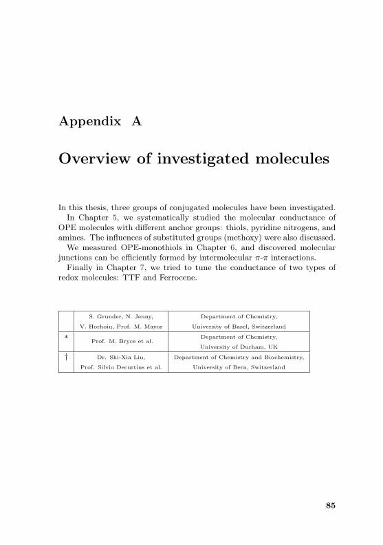
Appendix A
Overview of investigated molecules
In this thesis, three groups of conjugated molecules have been investigated.In Chapter 5, we systematically studied the molecular conductance of
OPE molecules with different anchor groups: thiols, pyridine nitrogens, andamines. The influences of substituted groups (methoxy) were also discussed.
We measured OPE-monothiols in Chapter 6, and discovered molecularjunctions can be efficiently formed by intermolecular π-π interactions.
Finally in Chapter 7, we tried to tune the conductance of two types ofredox molecules: TTF and Ferrocene.
S. Grunder, N. Jenny, Department of Chemistry,
V. Horhoiu, Prof. M. Mayor University of Basel, Switzerland
∗Prof. M. Bryce et al.
Department of Chemistry,
University of Durham, UK
† Dr. Shi-Xia Liu, Department of Chemistry and Biochemistry,
Prof. Silvio Decurtins et al. University of Bern, Switzerland
85
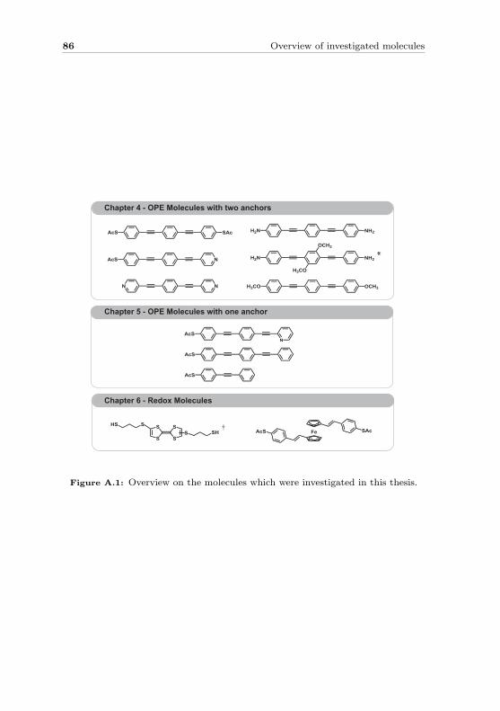
86 Overview of investigated molecules
Chapter 5 - OPE Molecules with one anchor
Chapter 6 - Redox Molecules
Chapter 4 - OPE Molecules with two anchors
AcS SAc
NAcS
N N
H2N NH2
H2N NH2
OCH3
H3CO
H3CO OCH3
S
S
S
SS
HS SSH
AcS
NAcS
AcS
Fe SAcAcS
*
†
Figure A.1: Overview on the molecules which were investigated in this thesis.
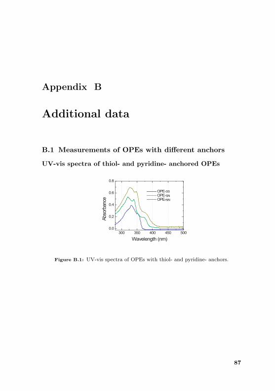
Appendix B
Additional data
B.1 Measurements of OPEs with different anchors
UV-vis spectra of thiol- and pyridine- anchored OPEs
300 350 400 450 5000.0
0.2
0.4
0.6
0.8
Abso
rban
ce
Wavelength (nm)
OPE-SS OPE-SN OPE-NN
Figure B.1: UV-vis spectra of OPEs with thiol- and pyridine- anchors.
87
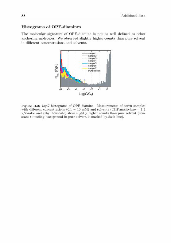
88 Additional data
Histograms of OPE-diamines
The molecular signature of OPE-diamine is not as well defined as otheranchoring molecules. We observed slightly higher counts than pure solventin different concentrations and solvents.
-6 -5 -4 -3 -2 -1 0
N logG (
logG
)
Log(G/G0)
sample1 sample2 sample3 sample4 sample5 sample6 sample7 Pure solvent
Figure B.2: logG histograms of OPE-diamine. Measurements of seven sampleswith different concentrations (0.1 − 10 mM) and solvents (THF:mesitylene = 1:4v/v-ratio and ethyl benzoate) show slightly higher counts than pure solvent (con-stant tunneling background in pure solvent is marked by dash line).
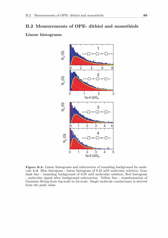
B.2. Measurements of OPE- dithiol and monothiols 89
B.2 Measurements of OPE- dithiol and monothiols
Linear histograms
0 2 4 6 8
N G (G)
0 1 2 3
N G (G)
1e-4 G/G0
2
0 1 2 3 4 5
N G (G)
N G (G)
1e-5 G/G0
3
0 1 2 3 4 5
1
4
Au-S S-Au
N-AuAu-S
NAu-S Ht
Au-S Ht
Figure B.3: Linear histograms and subtraction of tunneling background for mole-cule 1-4. Blue histogram - linear histogram of 0.25 mM molecular solution; Graydash line - tunneling background of 0.25 mM molecular solution; Red histogram- molecular signal after background subtraction. Yellow line - transformation ofGaussian fitting from log-scale to lin-scale. Single molecule conductance is derivedfrom the peak value.
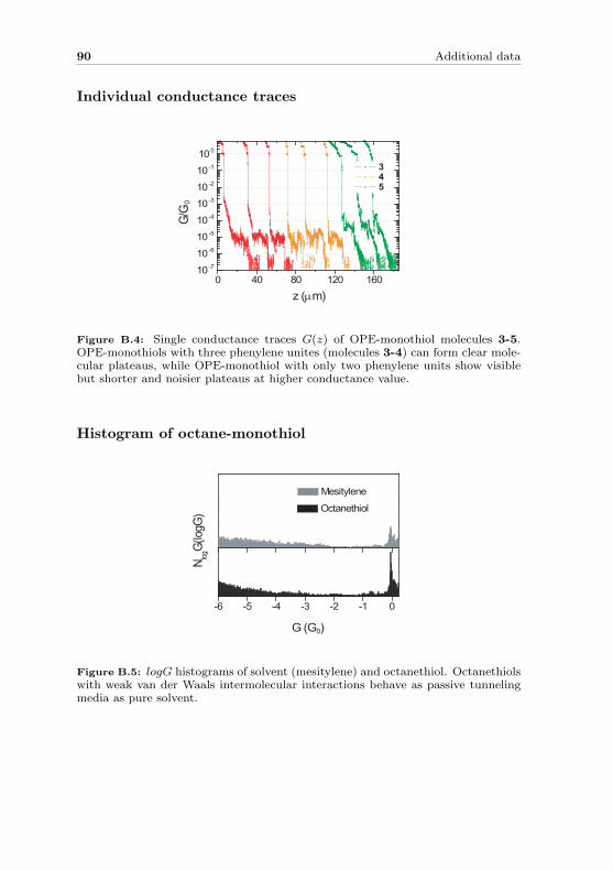
90 Additional data
Individual conductance traces
0 40 80 120 16010-7
10-6
10-5
10-4
10-3
10-2
10-1
100
3 4 5
G/G
0
z (µm)
Figure B.4: Single conductance traces G(z) of OPE-monothiol molecules 3-5.OPE-monothiols with three phenylene unites (molecules 3-4) can form clear mole-cular plateaus, while OPE-monothiol with only two phenylene units show visiblebut shorter and noisier plateaus at higher conductance value.
Histogram of octane-monothiol
-6 -5 -4 -3 -2 -1 0
Mesitylene
Octanethiol
N logG(
logG)
G (G0)
Figure B.5: logG histograms of solvent (mesitylene) and octanethiol. Octanethiolswith weak van der Waals intermolecular interactions behave as passive tunnelingmedia as pure solvent.
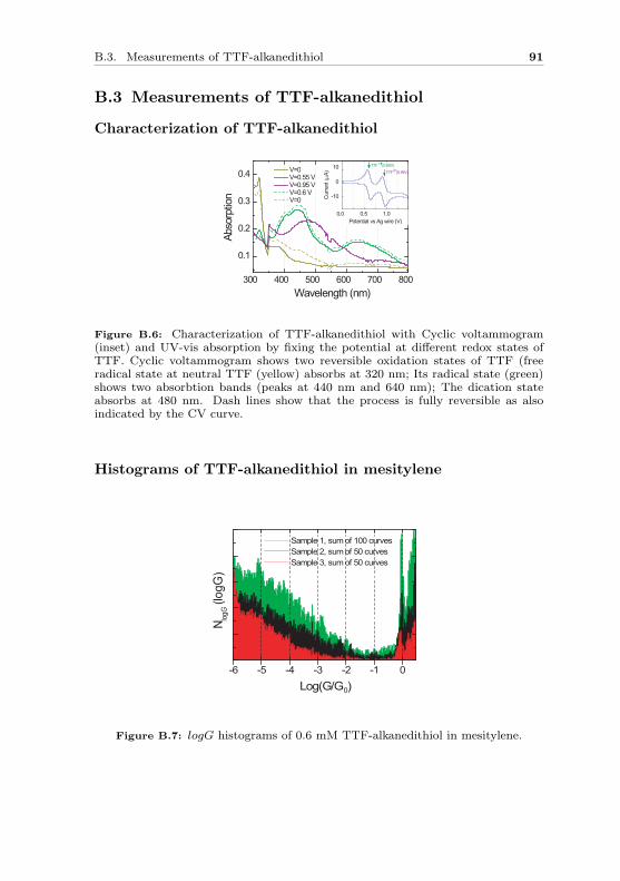
B.3. Measurements of TTF-alkanedithiol 91
B.3 Measurements of TTF-alkanedithiol
Characterization of TTF-alkanedithiol
300 400 500 600 700 800
0.1
0.2
0.3
0.4
Abso
rptio
n
Wavelength (nm)
V=0 V=0.55 V V=0.95 V V=0.6 V V=0
0.0 0.5 1.0
-10
0
10
Cur
rent
(µA)
Potential vs Ag wire (V)
TTF+ (0.60V)
TTF2+(0.95V)
Figure B.6: Characterization of TTF-alkanedithiol with Cyclic voltammogram(inset) and UV-vis absorption by fixing the potential at different redox states ofTTF. Cyclic voltammogram shows two reversible oxidation states of TTF (freeradical state at neutral TTF (yellow) absorbs at 320 nm; Its radical state (green)shows two absorbtion bands (peaks at 440 nm and 640 nm); The dication stateabsorbs at 480 nm. Dash lines show that the process is fully reversible as alsoindicated by the CV curve.
Histograms of TTF-alkanedithiol in mesitylene
-6 -5 -4 -3 -2 -1 0
N logG (
logG
)
Log(G/G0)
Sample 1, sum of 100 curves Sample 2, sum of 50 curves Sample 3, sum of 50 curves
Figure B.7: logG histograms of 0.6 mM TTF-alkanedithiol in mesitylene.

92 Additional data
Appendix C
Technical details
C.1 Sample fabrication
1. The substrate: To fabricate sample substrates, we use a flexiblespring steel plate, onto which an insulating polyimide layer, severalmicrometres thick, is cast. At first a 6.5× 6.5 cm piece of spring steelis cleaned in an acetone and afterwards isopropanol bath by using ofultrasonic agitation. Then 3 to 4 layers of polyimide (Pyralin PI2610HD Microsystem) are spun at 8000 rpm for 40 s on top of the metallicplate. After each layer the plate is baked at 200C for 40 min. Finally,the polyimide-covered plate is cured for 1 hr at 350C under 10−5
mbar. A laser cutting is used (Digipack AG, CH-8623 Wetzikon) tocut the covered steel plate to 24× 10 mm sample substrates.
2. E-beam lithography: Break junction structures are patterned by e-beam lithography. A layer of ∼ 600 nm positive resist (PMMA 950 K,Allresist GmbH, diluted with additional chlorbenzene) is spin-coatedonto the substrate (4000 rpm, 40 s), and baked at 175C for 30 min.After exposure with e-beam, the development is performed in a solu-tion of MIBK (4-methyl-2-pentanone) and isopropanol (1:3 v/v-ratio)for 45 s, followed by a rinse in isopropanol.
3. Metal deposition: We next mount the substrates in a vacuum cham-ber (PLS 500, Balzers-Pfeiffer GmbH) and evacuate down to∼ 10−6 mbar.After the sample holder is cooled down to ∼ 0C, we evaporate 10 nmtitanium layer at an angle of 50 and 60 nm gold layer perpendicularto the sample holder. This procedure ensures a good adhesion of thegold layer but avoids the presence of titanium in the central region
93
94 Technical details
of the bridge. Lift-off after evaporation is carried out in warm aceton(∼ 40).
4. Junction protection: In the case of electrochemical samples, themajor part of the Au surface needs to be protected to prevent leakagecurrent. We use polyimide photoresist (HD-4104, HD-microsystem) tocover the junction by standard photolithography. Polyimide photore-sist is first spin-coated onto the sample (4000 rpm, 60 s), and bakedat 85C for 2 min followed by at 95C for 2 min. After exposure anddevelopment, the sample is again cured for 1 hr at 350C under 10−5
mbar.
5. Under-etching: To obtain a free standing central metal bridge, thepolyimide is dry-etched in a reactive ion etching (RIE) machine (Plas-maLab 80 plus, Oxford). During the etching process the contact padsare covered by two glass slides. The exposed polyimide is slowly etchedaway which results in a hole under the central part of the Au bridge.The etching is performed at a flow of 2% CHF3 and 32% oxygen underpressure of 0.1 torr and at a power of 100 W for ∼ 3 min.
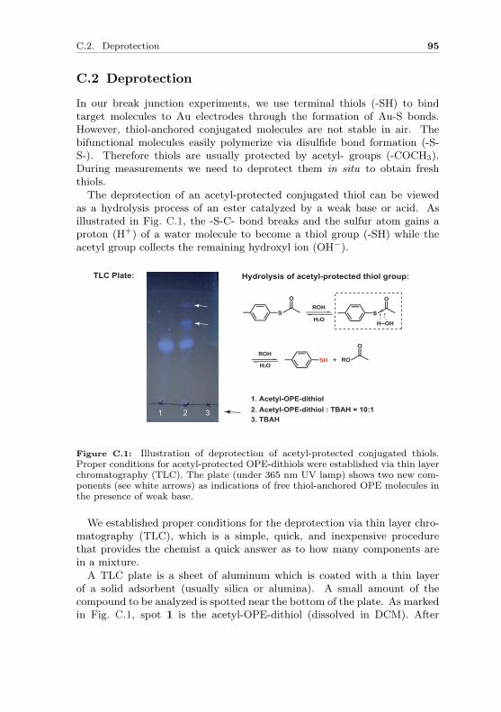
C.2. Deprotection 95
C.2 Deprotection
In our break junction experiments, we use terminal thiols (-SH) to bindtarget molecules to Au electrodes through the formation of Au-S bonds.However, thiol-anchored conjugated molecules are not stable in air. Thebifunctional molecules easily polymerize via disulfide bond formation (-S-S-). Therefore thiols are usually protected by acetyl- groups (-COCH3).During measurements we need to deprotect them in situ to obtain freshthiols.
The deprotection of an acetyl-protected conjugated thiol can be viewedas a hydrolysis process of an ester catalyzed by a weak base or acid. Asillustrated in Fig. C.1, the -S-C- bond breaks and the sulfur atom gains aproton (H+) of a water molecule to become a thiol group (-SH) while theacetyl group collects the remaining hydroxyl ion (OH−).
1 2 3
S
O
SH RO+
OHS
OHH
O
O
×
×
R
H2O
OHR
H2O
Hydrolysis of acetyl-protected thiol group:
1. Acetyl-OPE-dithiol 2. Acetyl-OPE-dithiol : TBAH = 10:13. TBAH
TLC Plate:
Figure C.1: Illustration of deprotection of acetyl-protected conjugated thiols.Proper conditions for acetyl-protected OPE-dithiols were established via thin layerchromatography (TLC). The plate (under 365 nm UV lamp) shows two new com-ponents (see white arrows) as indications of free thiol-anchored OPE molecules inthe presence of weak base.
We established proper conditions for the deprotection via thin layer chro-matography (TLC), which is a simple, quick, and inexpensive procedurethat provides the chemist a quick answer as to how many components arein a mixture.
A TLC plate is a sheet of aluminum which is coated with a thin layerof a solid adsorbent (usually silica or alumina). A small amount of thecompound to be analyzed is spotted near the bottom of the plate. As markedin Fig. C.1, spot 1 is the acetyl-OPE-dithiol (dissolved in DCM). After
96 Technical details
adding in ∼ 10% (mol) of TBAH (tetrabutylammonium hydroxide, dissolvedin THF), the mixture is spotted at position 2. TBAH is also spotted atposition 3 as a comparison. The plate is then placed in a shallow pool of asolution (cyclohexane:DCM = 1:1 v/v-ratio) so that only the very bottomof the plate is in the liquid. This liquid slowly rises up the TLC plateby capillary effect. As the solvent moves past the spot that was applied,the compounds in the mixture are separated due to different solubility andadsorption strength to the adsorbent. The plate is then removed from thedeveloping chamber, dried, and the conjugated components can be visualizedunder a UV lamp.
The TLC plate (Silica gel 60 F254 on aluminum sheets, MERCK) showsclearly two new components after deprotection which move higher up theplate (see white arrows). These are the hints of thiol-anchored OPE mole-cules, possibly the top one has free thiols on both ends and second-top onehas free thiol only on one end.
During deprotection, it is important to keep the solution under Ar in orderto prevent the formation of disulfide bonds. It can be observed on a TLCplate that the polymerized compounds are difficult to move up and remainat the spotted position.
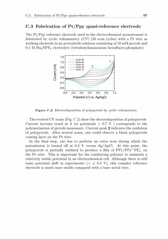
C.3. Fabrication of Pt/Ppy quasi-reference electrode 97
C.3 Fabrication of Pt/Ppy quasi-reference electrode
The Pt/Ppy reference electrode used in the electrochemical measurement isfabricated by cyclic voltammetry (CV) (50 scan cycles) with a Pt wire asworking electrode in an acetonitrile solution containing of 10 mM pyrrole and0.1 M Bu4NPF6 electrolyte (tetrabutylammonium hexafluoro-phosphate).
12
-0.6 -0.3 0.0 0.3 0.6 0.9 1.2
-0.8
-0.4
0.0
0.4
0.8
1.2
1.6Cu
rrent
(mA)
Potential (V) vs. Ag/AgCl
Cycle 50 Cycle 40 Cycle 30 Cycle 20 Cycle 10
Figure C.2: Electrodeposition of polypyrrole by cyclic voltammetry.
The evolved CV scans (Fig. C.2) show the electrodeposition of polypyrrole.Current increase trend at 1 (at potentials > 0.7 V ) corresponds to thepolymerization of pyrrole monomers. Current peak 2 indicates the oxidationof polypyrrole. After several scans, one could observe a black polypyrrolecoating layer on the Pt wire.
In the final step, one has to perform an extra scan during which thepotentiostat is turned off at 0.4 V versus Ag/AgCl. At this point, thepolypyrrole is partially oxidized to produce a film of PPy/PPy+PF−6 onthe Pt wire. This is important for the conducting polymer to maintain arelatively stable potential in an electrochemical cell. Although there is stillsome potential shift in experiments (∼ ± 0.2 V), this complex referenceelectrode is much more stable compared with a bare metal wire.

98 Technical details
Appendix D
Publication List
Articles
• S. Wu, R. Huber, J. Brunner, M. T. Gonzalez, S. Grunder, M. Mayor,C. Schonenberger and M. Calame, The role of contacts in molecularconductance: a comparison between thiol and pyridine, in preparation.
• J. Liao, Jon S. Agustsson, S. Wu, C. Schonenberger, M. Calame, S.X. Liu and S. Decurtins, Cyclic conductance switching in networks ofredox-active molecular junctions, to be published.
• S. Wu, M. T. Gonzalez, R. Huber, S. Grunder, M. Mayor, C. Schonenbergerand M. Calame, Molecular Junctions based on Aromatic Coupling, Na-ture Nanotech. 3, 569 (2008)
• R. Huber, M. T. Gonzalez, S. Wu, M. Langer, S. Grunder, V. Horhoiu,M. Mayor, M. Bryce, C. Wang, R. Jitchati, C. Schonenberger and M.Calame, Electrical conductance of conjugated oligomers at the singlemolecule level, JACS 130, 1080 (2008).
• Z. M. Wu, S. Wu, S. Oberholzer, M. Steinacher, M. Calame and C.Schonenberger, Scaling of 1/f noise in tunable break-junctions, Appl.Phys. Rev. B 78, 235421(2008).
• M. T. Gonzalez, J. Brunner, R. Huber, S. Wu, C. Schonenberger andM. Calame, Conductance values of alkanedithiol molecular junctions,New J. Phys. 10, 065018 (2008)
• M. T. Gonzalez, S. Wu, R. Huber, S. J. van der Molen, C. Schonenbergerand M. Calame, Electrical Conductance of Molecular Junctions by aRobust Statistical Analysis, Nano Letters 6, 2238 (2006).
99
100 Publication List
Poster contributions
• The role of contacts in molecular conductance: a comparison betweenthiol and pyridineS. Wu, R. Huber, M. T. Gonzalez, J. Brunner, S. Grunder, M. Mayor,C. Schonenberger and M. Calame,SwissNano Workshop 2009, Basel, Switzerland, Jun. 11th-12th, 2009.
• Break Junctions in Liquid for Molecular ElectronicsS. Wu, M. T. Gonzalez, R. Huber, S. Grunder, M. Mayor, S. X. Liuand S. Decurtins, C. Schonenberger and M. Calame.The 3rd AGEF - Euregio Workshop on Interfacial Electrochemistry,Rolduc Abbey, Kerkrade, Netherlands, Jun. 2nd - 3rd, 2008.
• Aromatic Induced Single Molecular JunctionsS. Wu, R. Huber, M. T. Gonzalez, S. Grunder, M. Mayor, C. Schonenbergerand M. Calame.Annual Meeting of the Swiss Physical Society, Geneva, Switzerland,Mar. 26th, 2008.
• Break Junctions in liquid for molecular electronicsR. Huber, S. Wu, M. T. Gonzalez, H. Breitenstein, P. Reimann, C.Schonenberger and M. Calame.International Workshop on Molecular Electronics, Rez, Prague, CzechRepublic, Jun. 30th - July 4th, 2006.
Oral presentations
• The Role of Contacts in Molecular ConductanceSwiss Workshop on Molecular Electronics, University of Bern, Switzer-land, May 12th, 2009.
• Molecular Junction Based on Aromatic CouplingThe 4th International Conference on Molecular Electronics: ELEC-MOL’08, Grenoble, France, Dec. 8th-12th 2008.
• Break Junctions in Liquid for Molecular ElectronicsThe 3rd AGEF - Euregio Workshop on Interfacial Electrochemistry,Rolduc Abbey, Kerkrade, Netherlands, Jun. 2nd - 3rd, 2008.
• Statistical Analysis of Single-Molecular-Junctions ConductanceNCCR Nano Meeting, PSI Villigen, Switzerland, Nov. 15th, 2006
Appendix E
Currriculum Vitae
Education
• 2005-presentPh.D. study in Nanoscience, Department of Physics, University ofBasel, Switzerland. Thesis: Electrical conductance of single conjugatedoligomers. Supervisor: Prof. Dr. C. Schonenberger.
• 2005M.Sc. in Material Science (Material Physics), Faculty of Engineering,Christian-Albrechts-University of Kiel, Germany. Thesis: Trenchedmetallized carbon nanotube composites for potential hydrogen sensorapplication. Supervisor: Prof. Dr. R. Adelung
• 2003M.Eng. in Material Science (Material Chemistry), Lab of InformationRecording Materials, Beijing Institute of Graphic Communication, P.R. China. Thesis: Synthesis and characterization of an acid-catalyzedhydrophilic-to-hydrophobic switching polymer. Supervisor: Prof. Dr.J.-L. Pu
• 2000B.Eng. in Polymer Materials and Engineering, Faculty of Chemi-cal Engineering, Beijing Institute of Petrochemical Technology, P. R.China.
101

102 Currriculum Vitae
Teaching experience
• 2008-2009 summer semestersPractical course Molecular Physics
• 2008 summer semesterPractical course for high school studentsQuantized Conductance in Atomic Contacts
• 2006-2007 summer semestersPractical course Cyclic Voltammetry
• 2006-2009 spring semestersPractical course General Physics for Beginners
Awards
• 2009Camille und Henry Dreyfus-Stipendium
• 2009Chinese Government Award For Outstanding Self-financed StudentsAbroad

Acknowledgements
I would like to thank here all the people who have helped me on this bothpainful and enjoyable journey of pursuing a Ph.D..
First and foremost, I express my sincere gratitude to Prof. Dr. ChristianSchonenberger, an inspiring and trusted supervisor, for giving me the op-portunity to work on this challenging topic and showing me a way to explorethe secrets of nature. Thank you for providing continuous guidance, adviceand support throughout the whole work.
I am deeply grateful to all the break junction team members: senior sci-entist Dr. Michel Calame, for your theoretical and experimental guidance,fruitful discussions and your constant care; Dr. Teresa Gonzalez and Dr.Roman Huber for your great contributions in building the setup and forsharing the knowledge of data analysis; Jan Brunner and Toni Frohlich, ournew members, for interesting discussions as well as your fresh mood. I wouldalso like to thank all the current and former members of the Nano-electronicsgroup for a friendly atmosphere.
I am thankful to our excellent chemists in Prof. Dr. Marcel Mayors’ group,especially Sergio Grunder, who actively synthesized most of molecules forour measurement and Yann Leroux, who brought the knowledge of electro-chemistry. I did not forget William Kylberg and Verena Thommen, for yourhelp on electrochemistry and photoelectrochemistry at my beginning stage.It is always cheerful to come over to discuss molecules with you.
Special thanks go to our mechanics workshop, Heinz Breitenstein andSilvester Jakob, for improving our setup, and electronics workshop aroundMichael Steinacher for the development of unique electronic devices.
Let me personally thank my hero, Jie Zeng, for your courage to facechanges, your optimism during hard time and the joys and dynamics youbring to our life. I am very much indebted to my parents, for your tremen-
103

104 Currriculum Vitae
dous but silent understanding and support.Finally I would like to thank the financial support provided by the NCCR
on Nanoscale Science.