Embed Size (px)
Citation preview

Full Version
Trends in Future-Oriented Sensor Technologies
Sensor Trends 2014
Published by:
AMA Association for Sensor TechnologySophie-Charlotten-Str. 15D-14059 Berlin, Germanyphone: +49 30 2219 0362-0fax: +49 30 2219 [email protected]
© AMA Fachverband für Sensorik e.V., July 2010
Editorial Team
Dr. Volker Großer Fraunhofer IZM, Berlin
Dr. Detlef Heydenbluth TU Ilmenau – IPMS
Prof. Dr. Ralf Moos Universität Bayreuth – LFM
Dr. Dirk Rein AMA Fachverband, Berlin
Josef Sauerer Fraunhofer IIS, Erlangen
Dr. C. Thomas Simmons AMA Fachverband, Berlin
Dr. Wolfgang Sinn IMMS GmbH, Ilmenau
Prof. Dr. Roland Werthschützky TU Darmstadt – EMK
Prof. Dr. Jürgen Wilde Universität Freiburg – IMTEK
Page 3
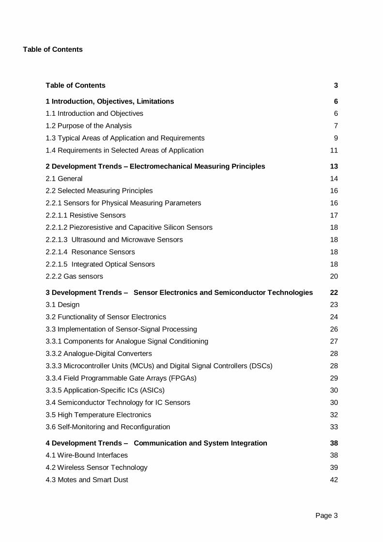
Table of Contents
Table of Contents 3
1 Introduction, Objectives, Limitations 6
1.1 Introduction and Objectives 6
1.2 Purpose of the Analysis 7
1.3 Typical Areas of Application and Requirements 9
1.4 Requirements in Selected Areas of Application 11
2 Development Trends – Electromechanical Measuring Principles 13
2.1 General 14
2.2 Selected Measuring Principles 16
2.2.1 Sensors for Physical Measuring Parameters 16
2.2.1.1 Resistive Sensors 17
2.2.1.2 Piezoresistive and Capacitive Silicon Sensors 18
2.2.1.3 Ultrasound and Microwave Sensors 18
2.2.1.4 Resonance Sensors 18
2.2.1.5 Integrated Optical Sensors 18
2.2.2 Gas sensors 20
3 Development Trends – Sensor Electronics and Semiconductor Technologies 22
3.1 Design 23
3.2 Functionality of Sensor Electronics 24
3.3 Implementation of Sensor-Signal Processing 26
3.3.1 Components for Analogue Signal Conditioning 27
3.3.2 Analogue-Digital Converters 28
3.3.3 Microcontroller Units (MCUs) and Digital Signal Controllers (DSCs) 28
3.3.4 Field Programmable Gate Arrays (FPGAs) 29
3.3.5 Application-Specific ICs (ASICs) 30
3.4 Semiconductor Technology for IC Sensors 30
3.5 High Temperature Electronics 32
3.6 Self-Monitoring and Reconfiguration 33
4 Development Trends – Communication and System Integration 38
4.1 Wire-Bound Interfaces 38
4.2 Wireless Sensor Technology 39
4.3 Motes and Smart Dust 42
Page 4
4.4 Autonomous Sensor Systems 43
5 Development Trends – Packaging 46
5.1 Housing Technologies, Encapsulation, Wafer-Level Packaging (31, 32) 47
5.2 Interconnect Devices and Substrates 55
5.3 Assembly Techniques 58
5.4 Bonding Techniques 60
5.5 New Integration Concepts 62
5.5.1 Sensor Structures in Structure Components and Clothing 62
5.5.2 Lab-on-a-Disk and Lab-on-Chip 63
5.5.3 Medical Technology 64
6 Development Trends – Testing Processes for MEMS Components 65
6.1 Fault Types 65
6.2 Wafer-Level Tests 68
6.3 Testing Equipment 71
6.3.1 Temperature Control 72
6.3.2 Physical Stimulation at Wafer Level 72
6.3.3 Basic Concepts of the Test Equipment 75
6.3.4 Tests at Wafer Level with Stimulation via Probe or Wafer Chuck 77
6.3.5 Tests at Wafer Level with Under-pressure or Overpressure 78
6.3.6 Application of Tests at Wafer Level 80
6.3.6.1 Gas Sensors 80
6.3.6.2 RF-MEMS 80
6.3.6.3 MEMS Infrared Arrays 81
6.4 Electrical Fault Detection and Self-Tests 81
6.4.1 Electrical Measurements 81
6.4.2 Built-In Self-Tests (BIST) 82
7 Glossary 84
7.1 Acronyms and Abbreviations 84
7.2 Terms 86
7.2.1 Faults and Failure of a Sensor 86
7.2.2 Measurement Parameter, Value and Signal 87
7.2.3 Measurement Uncertainty 87
7.2.4 Measuring Method 87
7.2.5 Measuring Principle 88
7.2.6 Measuring Process 88
Page 5
7.2.7 Output Signal 88
7.2.8 Primary Electronics 88
7.2.9 Secondary Electronics 89
7.2.10 Sensor 89
7.2.11 Sensor Characteristic 90
7.2.12 Sensor Element 90
7.2.13 Sensor Error 91
7.2.14 Sensor Network 91
7.2.15 Sensor Nodes 91
7.2.16 Sensor Reconfiguration 92
7.2.17 Sensor System 92
7.2.18 Sensor-Actuator System, Direct Coupling 92
7.2.19 Transducers and Transmitters 92
8 Bibliography 94

Page 6
1 Introduction, Objectives, Limitations
1.1 Introduction and Objectives
This study is a supplier-neutral overview from the AMA Association for Sensor Technology of
the expected short-term to medium-term technological developments in electromechanics
and gas-sensor technology. Its orientation is strictly technological and as such is not a mar-
keting study.
The aim of the study is to provide support to anyone who wants to obtain a quick overview of
the main technological developments behind the physical and gas-sensor technology, espe-
cially in view of feasible development strategies. The target groups comprise decision mak-
ers in high-technology fields, such as sensor suppliers and governmental agencies for fund-
ing programmes.
In practically all branches of industry and modern life, such as in mechanical and plant engi-
neering, the automotive and aerospace industries, entertainment and consumer industries,
medical technology and life sciences, as well as in safety and security technology, sensors
and measuring devices have become indispensible. In fact, there is hardly any industrial area
that can do without measuring, testing, monitoring, or automation. The value chain extends
from detection of process parameters in process technology to the analysis of product char-
acteristics in the entire productive industry. Sensors are to be found in ever growing numbers
even in everyday households. With the help of sensor technology, the ability to manufacture
products with unique features, but without significantly increasing production costs is more
and more successful.
In this high-tech area, Europe – and particularly Germany – are in the top position worldwide,
not only in regard to the technological standard, but also in view of global market shares. As
for turnover, a comparison between commercial studies regarding the demand (see (1) or (2)
for example) and the results of the polls carried out by the AMA Association (3) regarding the
supplier market, shows that European suppliers cover about 35% of the worldwide demand
on sensor products (4).
The number of manufacturers of industrial sensors and measuring systems in Europe alone
is estimated by the AMA Association for Sensor Technology to comprise almost 1,000 enter-
prises. Overall there are approximately 3,000 companies from makers to retailers, from engi-
neering consultants to specialized service providers that are active in European sensor tech-
Page 7
nology. The figure for jobs directly in measuring technology, not counting peripheral equip-
ment or peripheral activities, is estimated at 290,000 employees in Germany alone. With
sales and sensor-specific services they generate 30 to 40 billion euros. At an average yearly
rate of 9% (not including the years 2008 and 2009), the growth of European sensor technol-
ogy is about four times as fast as the EU economy as a whole. Even in the crisis year 2009,
the German export quota of sensor and measuring technology achieved 47%. If we include
the additional indirect exports of machines, plant equipment, and other products, in which
sensor and measuring systems are integrated, it can be surmised that approximately 80% of
the German sensor and measuring equipment is exported.
The biggest sensor trade fair is the annual SENSOR+TEST in Nuremberg, an event organ-
ized under the auspices of the European AMA Association. All in all, Europe is thus among
the worldwide top sensor suppliers, not only in regard to turnover, but also in view of the ca-
pability of technological innovation.
The market for sensor technology is very inhomogeneous and very hard to segment even for
those involved. These, however, are experiencing a noticeable shift from the market for capi-
tal goods to the market for consumer goods with an increasing importance of end products.
Therefore, the market for sensors in consumer end products is generally growing at a faster
rate than for those in process measuring and control technology. New applications with con-
siderable growth rates are found in household appliances, safety and security technology,
medical equipment for diagnosis and therapy, biosensorics, and automotive engineering. The
greatest growth rates, however, are to be found in image sensors, acceleration sensors,
pressure sensors, position and proximity sensors as well as in biochemical sensors. All in all,
prices can be said to be falling, while quantities are rising.
1.2 Purpose of the Analysis
Using selected areas of application as examples, this study bundles the experience of the
authors from the research facilities organized within the AMA Association Science Board.
The focus is not on completeness, but rather on the elaboration of some major trends. The
paper considers development trends in sensor technology for measuring mechanical, calo-
rific, and chemical parameters, such as pressure, flow, temperature, distance, speed, accel-
eration, force, torque, ph-value, concentration and composition of gases and liquids.

Page 8
The focal points are:
Principles for measuring physical, chemical, and biological parameters
Electronic assembly and packaging
Functions and methods of signal processing
Sensor-signal interfaces and transfer, including wireless transmission with autono-
mous energy management, bidirectional communication, and networks
System integration: sensor systems and directly coupled sensor-actuator systems
Interference tolerance of sensors and sensor systems: automated fault detection, di-
agnosis, and correction (AFDDC)
Testing and calibration technology
Due to the extremely broad application spectrum of sensor technology in all branches of in-
dustry and fields of application – from R&D and automated production to control and monitor-
ing of product characteristics – the study is limited to the following areas of application, which
are to serve as examples:
Process, energy, and environmental engineering
Mechanical engineering
Automotive engineering
Medical technology / life sciences
Consumer goods
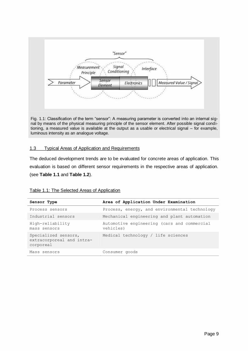
The Terms “Sensor” and “Measuring Principle”
The term “sensor” is variously interpreted. In this study, it is used as a superordinate term
describing any component that generates a usable electrical signal from a measured physi-
cal parameter, as illustrated in Fig. 1.1. In its simplest form, a sensor consists merely of a
naked sensor element, for instance an unhoused pressure sensor element made of silicon,
mounted on a substrate, no more than a few millimetres exterior dimension.
The term “measuring principle” (also referred to as the “active principle”) is understood to
mean the principle of physical or chemical conversion resulting in a usable electrical signal.
Further terms used in this study are defined in the Glossary, Chapter 7.
Page 9
Fig. 1.1: Classification of the term “sensor”: A measuring parameter is converted into an internal sig-nal by means of the physical measuring principle of the sensor element. After possible signal condi-tioning, a measured value is available at the output as a usable or electrical signal – for example, luminous intensity as an analogue voltage.
1.3 Typical Areas of Application and Requirements
The deduced development trends are to be evaluated for concrete areas of application. This
evaluation is based on different sensor requirements in the respective areas of application.
(see Table 1.1 and Table 1.2).
Table 1.1: The Selected Areas of Application
Sensor Type Area of Application Under Examination
Process sensors Process, energy, and environmental technology
Industrial sensors Mechanical engineering and plant automation
High-reliability
mass sensors
Automotive engineering (cars and commercial
vehicles)
Specialized sensors,
extracorporeal and intra-
corporeal
Medical technology / life sciences
Mass sensors Consumer goods
Page 10
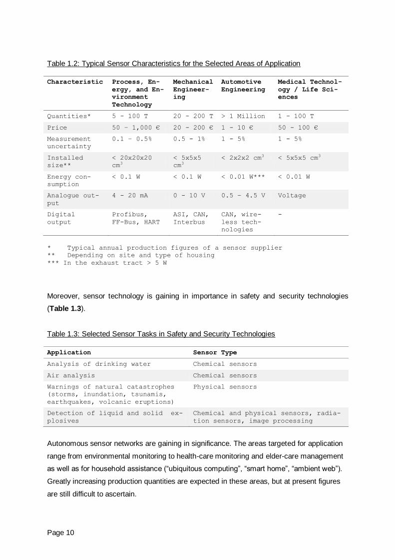
Table 1.2: Typical Sensor Characteristics for the Selected Areas of Application
Characteristic Process, En-
ergy, and En-
vironment
Technology
Mechanical
Engineer-
ing
Automotive
Engineering
Medical Technol-
ogy / Life Sci-
ences
Quantities* 5 - 100 T 20 - 200 T > 1 Million 1 - 100 T
Price 50 – 1,000 € 20 - 200 € 1 - 10 € 50 - 100 €
Measurement
uncertainty
0.1 – 0.5% 0.5 - 1% 1 - 5% 1 - 5%
Installed
size**
< 20x20x20
cm3
< 5x5x5
cm3
< 2x2x2 cm3 < 5x5x5 cm3
Energy con-
sumption
< 0.1 W < 0.1 W < 0.01 W*** < 0.01 W
Analogue out-
put
4 - 20 mA 0 - 10 V 0.5 – 4.5 V Voltage
Digital
output
Profibus,
FF-Bus, HART
ASI, CAN,
Interbus
CAN, wire-
less tech-
nologies
-
* Typical annual production figures of a sensor supplier
** Depending on site and type of housing
*** In the exhaust tract > 5 W
Moreover, sensor technology is gaining in importance in safety and security technologies
(Table 1.3).
Table 1.3: Selected Sensor Tasks in Safety and Security Technologies
Application Sensor Type
Analysis of drinking water Chemical sensors
Air analysis Chemical sensors
Warnings of natural catastrophes
(storms, inundation, tsunamis,
earthquakes, volcanic eruptions)
Physical sensors
Detection of liquid and solid ex-
plosives
Chemical and physical sensors, radia-
tion sensors, image processing
Autonomous sensor networks are gaining in significance. The areas targeted for application
range from environmental monitoring to health-care monitoring and elder-care management
as well as for household assistance (“ubiquitous computing”, “smart home”, “ambient web”).
Greatly increasing production quantities are expected in these areas, but at present figures
are still difficult to ascertain.
Page 11
1.4 Requirements in Selected Areas of Application
Basic user requirements and wishes in regard to sensors are (5):
Attainment of minimal measuring uncertainty
Constant availability of physical and chemical data from all systems and processes
Measurements are to be performed with minimal impact on the processes involved
Measuring values are to be available in real time
Sensors should function without maintenance, calibration, or adjustment
Sensor should work with minimal interference and a minimum of care
Sensor and sensor-system costs should be as low as possible
Sensors are to be equipped with integrated “on-board” diagnostics
In this context we are able to perceive that some of the requirements are contradictory, e.g.
minimal measuring uncertainty vs. cost. Typical requirements and their evaluation as to qual-
ity according to selected fields of application are listed in Table 1.4.
Page 12
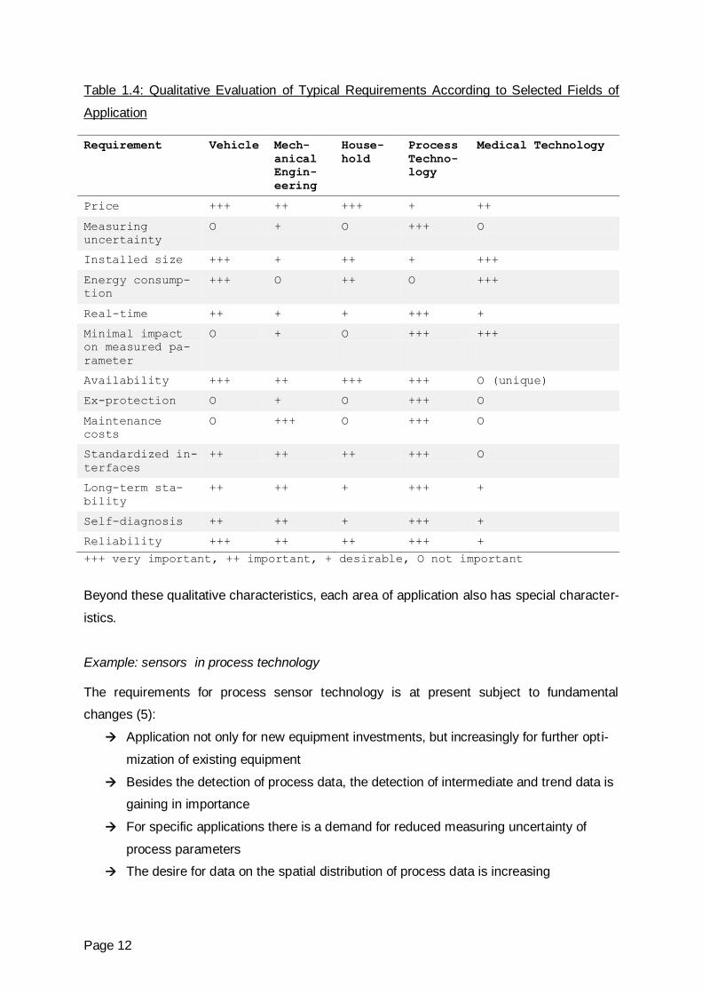
Table 1.4: Qualitative Evaluation of Typical Requirements According to Selected Fields of
Application
Requirement Vehicle
Mech-
anical
Engin-
eering
House-
hold
Process
Techno-
logy
Medical Technology
Price +++ ++ +++ + ++
Measuring
uncertainty
O + O +++ O
Installed size +++ + ++ + +++
Energy consump-
tion
+++ O ++ O +++
Real-time ++ + + +++ +
Minimal impact
on measured pa-
rameter
O + O +++ +++
Availability +++ ++ +++ +++ O (unique)
Ex-protection O + O +++ O
Maintenance
costs
O +++ O +++ O
Standardized in-
terfaces
++ ++ ++ +++ O
Long-term sta-
bility
++ ++ + +++ +
Self-diagnosis ++ ++ + +++ +
Reliability +++ ++ ++ +++ +
+++ very important, ++ important, + desirable, O not important
Beyond these qualitative characteristics, each area of application also has special character-
istics.
Example: sensors in process technology
The requirements for process sensor technology is at present subject to fundamental
changes (5):
Application not only for new equipment investments, but increasingly for further opti-
mization of existing equipment
Besides the detection of process data, the detection of intermediate and trend data is
gaining in importance
For specific applications there is a demand for reduced measuring uncertainty of
process parameters
The desire for data on the spatial distribution of process data is increasing
Page 13
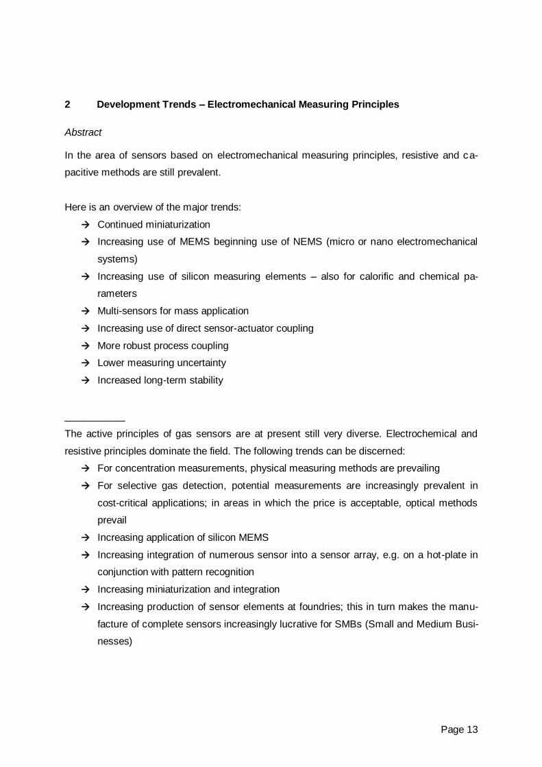
2 Development Trends – Electromechanical Measuring Principles
Abstract
In the area of sensors based on electromechanical measuring principles, resistive and ca-
pacitive methods are still prevalent.
Here is an overview of the major trends:
Continued miniaturization
Increasing use of MEMS beginning use of NEMS (micro or nano electromechanical
systems)
Increasing use of silicon measuring elements – also for calorific and chemical pa-
rameters
Multi-sensors for mass application
Increasing use of direct sensor-actuator coupling
More robust process coupling
Lower measuring uncertainty
Increased long-term stability
__________
The active principles of gas sensors are at present still very diverse. Electrochemical and
resistive principles dominate the field. The following trends can be discerned:
For concentration measurements, physical measuring methods are prevailing
For selective gas detection, potential measurements are increasingly prevalent in
cost-critical applications; in areas in which the price is acceptable, optical methods
prevail
Increasing application of silicon MEMS
Increasing integration of numerous sensor into a sensor array, e.g. on a hot-plate in
conjunction with pattern recognition
Increasing miniaturization and integration
Increasing production of sensor elements at foundries; this in turn makes the manu-
facture of complete sensors increasingly lucrative for SMBs (Small and Medium Busi-
nesses)
Page 14
2.1 General
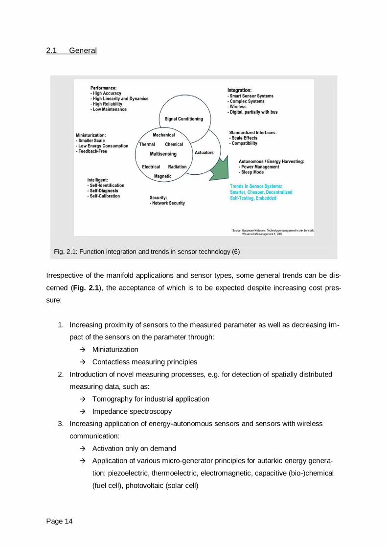
Fig. 2.1: Function integration and trends in sensor technology (6)
Irrespective of the manifold applications and sensor types, some general trends can be dis-
cerned (Fig. 2.1), the acceptance of which is to be expected despite increasing cost pres-
sure:
1. Increasing proximity of sensors to the measured parameter as well as decreasing im-
pact of the sensors on the parameter through:
Miniaturization
Contactless measuring principles
2. Introduction of novel measuring processes, e.g. for detection of spatially distributed
measuring data, such as:
Tomography for industrial application
Impedance spectroscopy
3. Increasing application of energy-autonomous sensors and sensors with wireless
communication:
Activation only on demand
Application of various micro-generator principles for autarkic energy genera-
tion: piezoelectric, thermoelectric, electromagnetic, capacitive (bio-)chemical
(fuel cell), photovoltaic (solar cell)
Page 15
Networked miniaturized measuring sites for collective detection of measuring
values and transmission
4. Increasing system integration for mechatronic applications:
Transition to directly coupled sensor-actuator systems for detection and con-
trol of local process parameters
5. Increasing holistic sensor design:
Utilization of novel 3D design tools, FEM (finite elements method) computa-
tion, Matlab/Simulink, use of comprehensive and exact material data
6. Increasing functional integration based on highly integrated components in sensor
electronics and safeguarding of the expanded functionality:
Pattern detection, additional data acquisition
Self-monitoring
Interference detection and diagnosis
Self-calibration (self-adjustment) and reconfiguration
Derivation of data for preventive maintenance
Integrated communication interface
(TEDS, IEEE 1451)
Plug and play
Localization (positioning)
7. Utilization of highly integrated components for real-time signal conditioning and proc-
essing:
High resolution and fast A/D conversion
Single-chip microprocessors
µC, FPGA, DSSP (digital sensor-signal processor)
Programmable logic devices (PLDs)
Semiconductor memories
Coupling modules for electrical interfaces (wired, wireless)
8. Coupling of physical, chemical, and biological sensors on a single sensor element,
e.g. for pressure measurement, pH-value measurement (animal husbandry), lab on a
chip, lab on a disc
9. Increasing production of sensor elements by specialized suppliers (foundries); thus
making production of complete sensors increasingly lucrative for SMBs
Page 16
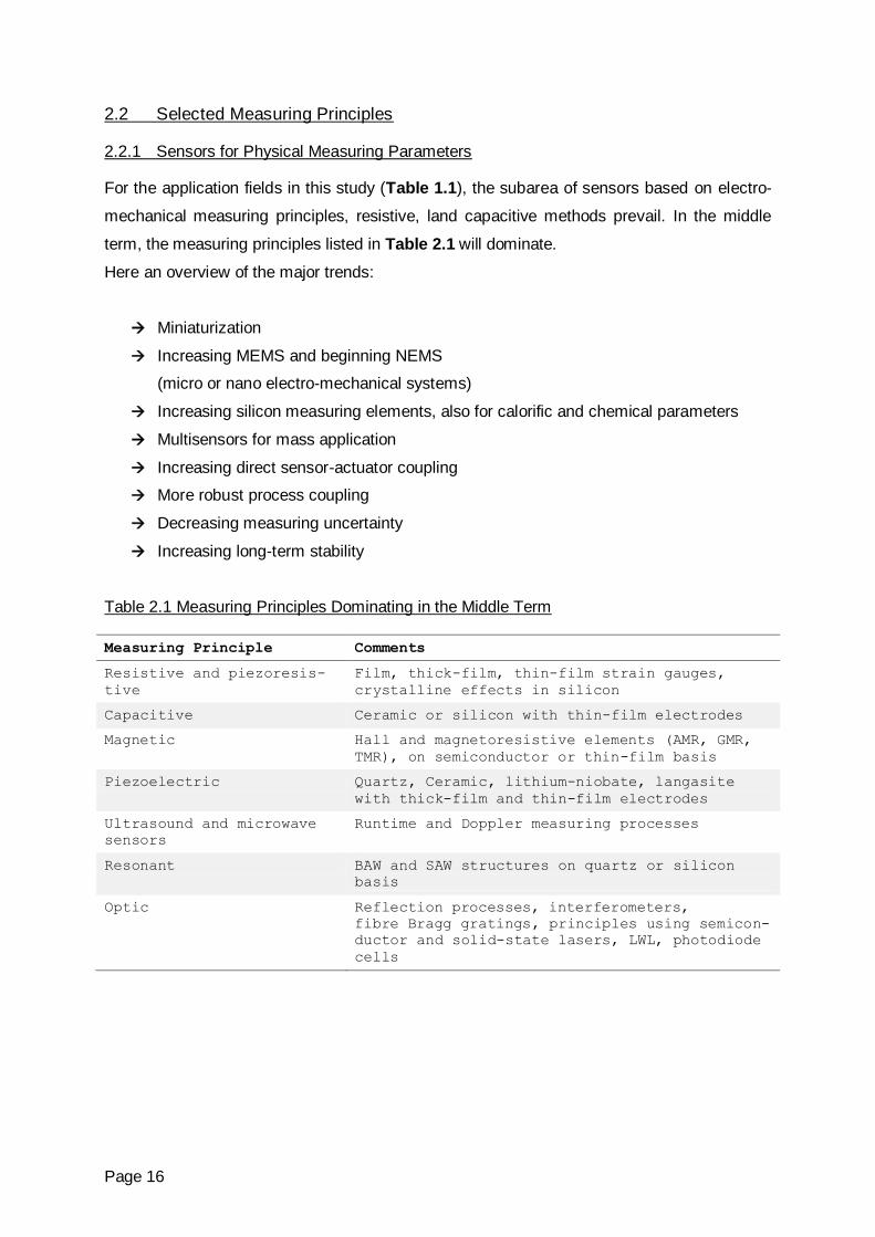
2.2 Selected Measuring Principles
2.2.1 Sensors for Physical Measuring Parameters
For the application fields in this study (Table 1.1), the subarea of sensors based on electro-
mechanical measuring principles, resistive, land capacitive methods prevail. In the middle
term, the measuring principles listed in Table 2.1 will dominate.
Here an overview of the major trends:
Miniaturization
Increasing MEMS and beginning NEMS
(micro or nano electro-mechanical systems)
Increasing silicon measuring elements, also for calorific and chemical parameters
Multisensors for mass application
Increasing direct sensor-actuator coupling
More robust process coupling
Decreasing measuring uncertainty
Increasing long-term stability
Table 2.1 Measuring Principles Dominating in the Middle Term
Measuring Principle Comments
Resistive and piezoresis-
tive
Film, thick-film, thin-film strain gauges,
crystalline effects in silicon
Capacitive Ceramic or silicon with thin-film electrodes
Magnetic Hall and magnetoresistive elements (AMR, GMR,
TMR), on semiconductor or thin-film basis
Piezoelectric Quartz, Ceramic, lithium-niobate, langasite
with thick-film and thin-film electrodes
Ultrasound and microwave
sensors
Runtime and Doppler measuring processes
Resonant BAW and SAW structures on quartz or silicon
basis
Optic Reflection processes, interferometers,
fibre Bragg gratings, principles using semicon-
ductor and solid-state lasers, LWL, photodiode
cells
Page 17
The following trends can be discerned in physical measuring principles:
1. Among the sensors for mechanical parameters, resistive and capacitive methods
maintain their present prevalence
2. Decreasing measuring uncertainty for selected applications by optimizing packaging
technology and retroactive impact on the measuring value
3. Increasing application of silicon as a substance for measuring elements for various
physical parameters, besides pressure and acceleration, also force, humidity, and
temperature
4. Utilization of silicon allows further reduction of sensor-element size by application of
micromechanics
5. Use of electromechanical converters, such as Si-pressure plates or Si-cantilevers for
detecting calorific (humidity, temperature) and chemical parameters, e.g. with pie-
zoresistive measuring elements and sensitive polymer coating
6. Increasing utilization of silicon multi-sensors for mass applications
7. Detection of multiple measuring values with a single sensor element
8. Detection of spatial distribution measuring parameters by means of sensor arrays
9. Increasing directly coupled sensor-actuator systems, e.g. optical scanner systems
(DVD), control valves (pressure, flow, settings parameters, ...), micro-positioning sys-
tems, (smart) orthotic and prosthetic, haptic displays, etc.
10. Great increase in application of micro and lately also of nano electromechanical sys-
tems (MEMS and NEMS)
Here an itemized list of prevalent development trends:
2.2.1.1 Resistive Sensors
This includes stain gauges, thick-film, thin-film on metallic deformation elements or ceramics.
The relative proportion of these principles will remain nearly stable.
Foil strain gauges (k-factor approx. 2):
Pressure sensors (1 to 5.000 bar), force and torque
Miniaturized foil gauges < 2 x 2 mm²
Novel substrate and conductor materials
Continued development of deformation elements, novel materials
Integration in machine components (adaptronics) and textiles, e.g. in carbon
fibres
Page 18
Thick-film resistors on ceramic substrates:
Pressure sensors (1 to 100 bar)
Pastes with high k-factor > 10
Deformation elements with LTTC ceramics (flexible forming, also for low pro-
duction quantities, capability of establishing electric contacts)
Thin-film resistors (k-factor 2 to 3) with isolating layers on metallic deformation ele-
ments:
Pressure (0.1 to 1,000 bar), force and torque sensors
Optimization of substrates and passivation layers
2.2.1.2 Piezoresistive and Capacitive Silicon Sensors
Continued miniaturization, e.g. pressure sensor elements with a surface area < 0.5 x
0.5 mm²
Integration into sensor systems with low energy consumption
Application of the capacitive principle in precision sensors as differential capacitors
with defined dielectric
Direct allocation of primary electronics as a single-chip or two-chip solution
2.2.1.3 Ultrasound and Microwave Sensors
Ultrasound silicon miniature sensors with an area of < 1 x 1 mm²
Configuration into an ultrasound sensor array with directional radio effect
Tomography with ultrasound and/or microwave methods
2.2.1.4 Resonance Sensors
Miniaturized quartz or silicon bulk acoustic wave (BAW) sensors
Surface acoustic wave (SAW) sensors
Use of new materials, such as lithium-niobate, langasite, etc. (greater temperature
ranges)
2.2.1.5 Integrated Optical Sensors
Bragg fibre grating arrays for strain gauges and temperature measurement
Miniaturized optical solid-state resonators on semiconductor basis, e.g. neodymium
YAG (yttrium-aluminium-garnet) crystals
Miniaturized spectrometers, fully adjustable semiconductor lasers
Page 19
Special Significance of Silicon as a Measuring Element Material
Based on its excellent elastic characteristics as well as its very good selectivity in regard to
electrical and chemical attributes, silicon will continue to gain significance as a substance for
sensor elements. The following trends are expected especially for these sensors and their
associated measuring principles:
Increasing significance for measurement of various physical parameters, such as
pressure, acceleration, and force, but also of humidity and temperature
Continued increase in the importance of electromechanical transducers, such as Si
pressure plates or Si cantilevers for determining various parameters (piezoresistive
measuring element + sensitive coatings)
Wide-spread application thanks to minimal dimensions of sensor arrays for determin-
ing local distribution of a given parameter (applications: automotive engineering,
medical technology, household appliances, safety and security technology, medical
care, etc.)
Integration of sensor electronic components / primary electronics into the silicon ele-
ment itself
Greater use of silicon multisensors for determining various physical parameters simul-
taneously, e.g. differential pressure, static pressure and media temperature
For mass applications with multiple measuring parameters on a single sensor
element
For bundling physical, chemical, and biological sensors on a single sensor
element, e.g. pressure + pH-value measurement (animal husbandry), lab on a
chip, lab on disc, etc.
Special development trends, such as:
Further miniaturization, e.g. on surface areas < 0.5 x 0.5 mm² (medical tech-
nology)
Increased stability of monocrystalline and polycrystalline structures
Application of porous silicon layers for the production of deformation elements,
e.g. pressure plates
Extended temperature ranges of up to 350 °C (SOI deposition)
Transition from volume micromechanics to surface micromechanics
Extended pressure ranges of up to 5,000 bar
Piezoresistive miniature force sensors
Page 20
Piezoresistive full-bridge strain gauges on steel elements with integrated pri-
mary electronics
Determination of moisture and pH-value (through the swelling of polymer coat-
ings)
2.2.2 Gas sensors
Sensor Elements
The active principles of gas sensors are at present still very diverse. As yet there is no single
technological approach, such as e.g. silicon micromechanics for physical sensors. Usually,
the technology involved is adapted to the specific application and to the available in-house
technology at the sensor supplier. Nevertheless, some technological trends can be discerned
and described with the keywords miniaturization and integration. Electrochemical and resis-
tive principles dominate the field:
For concentration measurements, physical measuring methods are taking hold
For selective gas detection, potential measurements hold sway in case of cost-critical
applications; when prices are acceptable or if demanded by the application, optical
methods are used
Increasing use of silicon MEMS (hot plates)
Increasing integration of multiple sensors on a single hot plate (sensor arrays), also
used for pattern detection
Increasing miniaturization and integration
Two general development trends in sensor elements for chemical parameters are:
1. Thanks to improved reproducibility and long-term stability of available sensors, the
chemical parameters gas concentration and liquid concentration can be measured by
means of physical methods. The signal conditioning involved is often expensive, but
is getting cheaper.
2. New measuring tasks and requirements are constantly arising, the solution of which
are at present being realized by contending principles. Usually, the most inexpensive
system is used – after a holistic selection taking the cost aspect into account.
Just as for physical sensors, transducers are being increasingly produced in silicon micro-
mechanics (hot plates). Since foundries are now able to supply silicon micromechanics, this

Page 21
technology is increasingly suited for MSBs. The transition to silicon micromechanics is not
only due to the availability of inexpensive mass production, but also due to the inherent ad-
vantages offered by silicon micromechanics, such as a reduced energy consumption, which
in turn enables battery powered operation, or the ability for thermal cycling, which allows an
increase in selectivity. Based on the same principle, thermal conductivity sensors can be
made for H2 detection.
In research, even higher application temperatures are being used, e.g. by high-temperature
Si hotplates. SiC micro-hotplates, or low-temperature co-fired ceramic (LTCC) hotplates.
The trend is towards the integration of multiple sensors on a single hotplate (sensor arrays).
Thanks to pattern recognition, new applications can be opened in such areas as:
Safe and early fire detection
Medical technology
Food selection
Quality assurance in the life-sciences industry
Depending on the specific application, these may be in combination with 3D-MID or microflu-
idic elements.
In the near future the following tendencies will compliment rather than replace the present
sensor principles:
Potential instead of resistive measurements
Novel workfunction based sensors for selective gas detection at ambient tempera-
tures are already being developed; direct and indirect thermoelectric gas sensors for
detection of VOCs are being developed.
Optical methods
Promising are attempts to apply optical principles for selective sensors. Examples are
NH3 or O2 detection with the aid of laser diodes, or CO2 sensors based on miniatur-
ized NDIR systems priced for consumer goods. Whether the laser-diode technology
will hold sway depends to a certain degree on the price tendency of laser diodes, but
also on the attained degree of system miniaturization. For the measurement of minute
concentrations, the long optical path may lose out to cost-effective miniaturization.

Page 22
Methods for selectivity increase
For increasing selectivity, attempts are being made to apply catalytic filters and/or ab-
sorption filters; work on micro-gas chromatographs (µ-GC) were also successful.
Thermal cycling of the sensor temperature can also increase selectivity if evaluated
accordingly. These processes can also be combined with the use of sensor arrays.
The same applies for chemical sensor systems as for physical sensors. A/D conversion and
sensors are being brought closer together. Analogue signal conditioning is increasingly being
replaced by digital signal processing in a very early state. Whenever cost-effective, sensors
and signal processing are being integrated in a single housing. In a way, the µC is thus be-
coming a part of the sensor component. By such means, characteristics, such as bus capa-
bility, self-monitoring, or even self-calibration can be realized.
In automotive engineering, the two-wire principle (CAN bus) with a current signal will in part
prevail.
3 Development Trends –
Sensor Electronics and Semiconductor Technologies
Abstract
In general it can be observed that the relatively simple sensors of the past are turning into
increasingly integrated and intelligent sensor systems boasting hardware with ever greater
capabilities. Depending on the application, signal conditioning is analogue, digital, or pro-
vided as a mixed signal. The trend is towards early digitalization and digital signal process-
ing. The functionality of the sensor is increasing. Sensors are increasingly able to perform
correction computations, compensate cross-sensitivity, provide application-specific algo-
rithms, carry out self-monitoring, and contain their own communication interface. This greater
capability also includes:
Faster signal processing with a lower noise level and higher resolution
Lower energy consumption
Greater maximum ambient temperatures
More compact dimensions
Increasingly reports on error states or threshold values instead of the mere transmis-
sion of measured values
__________

Page 23
In the majority of applications after electronic conversion of the measuring parameter this is
also processed. Improvements and innovations in sensors are thus being attained more and
more not only by further development of the measuring element itself, but through parallel
development of the primary electronics and sensor-specific signal processing. By effectively
optimizing the primary sensor, signal conditioning, and signal processing, a greater efficiency
can be achieved than would be possible by only optimizing the measuring element itself.
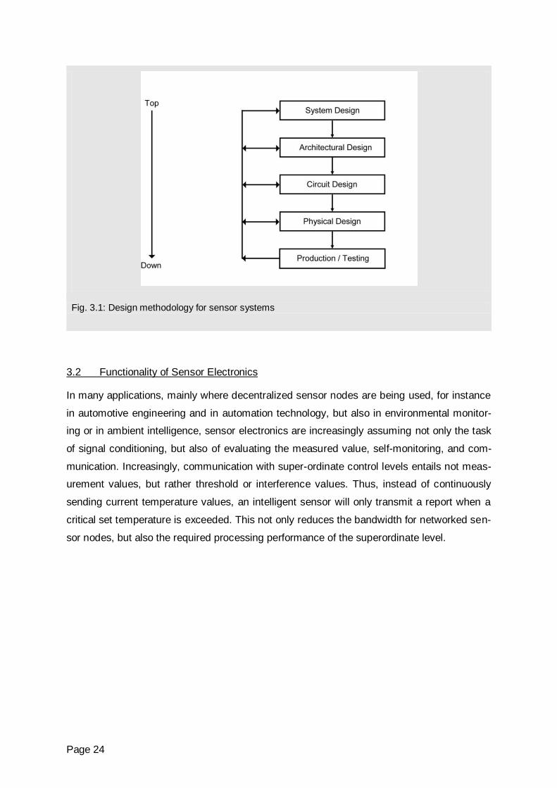
3.1 Design
In regard to the design of sensor electronics, the following trends may be observed:
1. System design, architectural design, and circuit design increasingly mesh and are
becoming more complex. The development of sensor systems is tending towards:
Ever higher resolution
Increasing complexity, e.g. due to local performance of data reduction, more
efficient interfaces, etc.
Greater sophistication of compensation, linearization, calibration, and signal
processing
2. Sensor-system design is generally top down (Fig. 3.1):
Specifications and verification as early as possible at various levels of abstrac-
tion
Step-by-step system simulation
3. In order to design complex systems more effectively, IPs (digital function blocks and
analogue macrocells) are used. These must be represented at different abstraction
levels to enable corresponding simulations.
Page 24
Fig. 3.1: Design methodology for sensor systems
3.2 Functionality of Sensor Electronics
In many applications, mainly where decentralized sensor nodes are being used, for instance
in automotive engineering and in automation technology, but also in environmental monitor-
ing or in ambient intelligence, sensor electronics are increasingly assuming not only the task
of signal conditioning, but also of evaluating the measured value, self-monitoring, and com-
munication. Increasingly, communication with super-ordinate control levels entails not meas-
urement values, but rather threshold or interference values. Thus, instead of continuously
sending current temperature values, an intelligent sensor will only transmit a report when a
critical set temperature is exceeded. This not only reduces the bandwidth for networked sen-
sor nodes, but also the required processing performance of the superordinate level.
Page 25
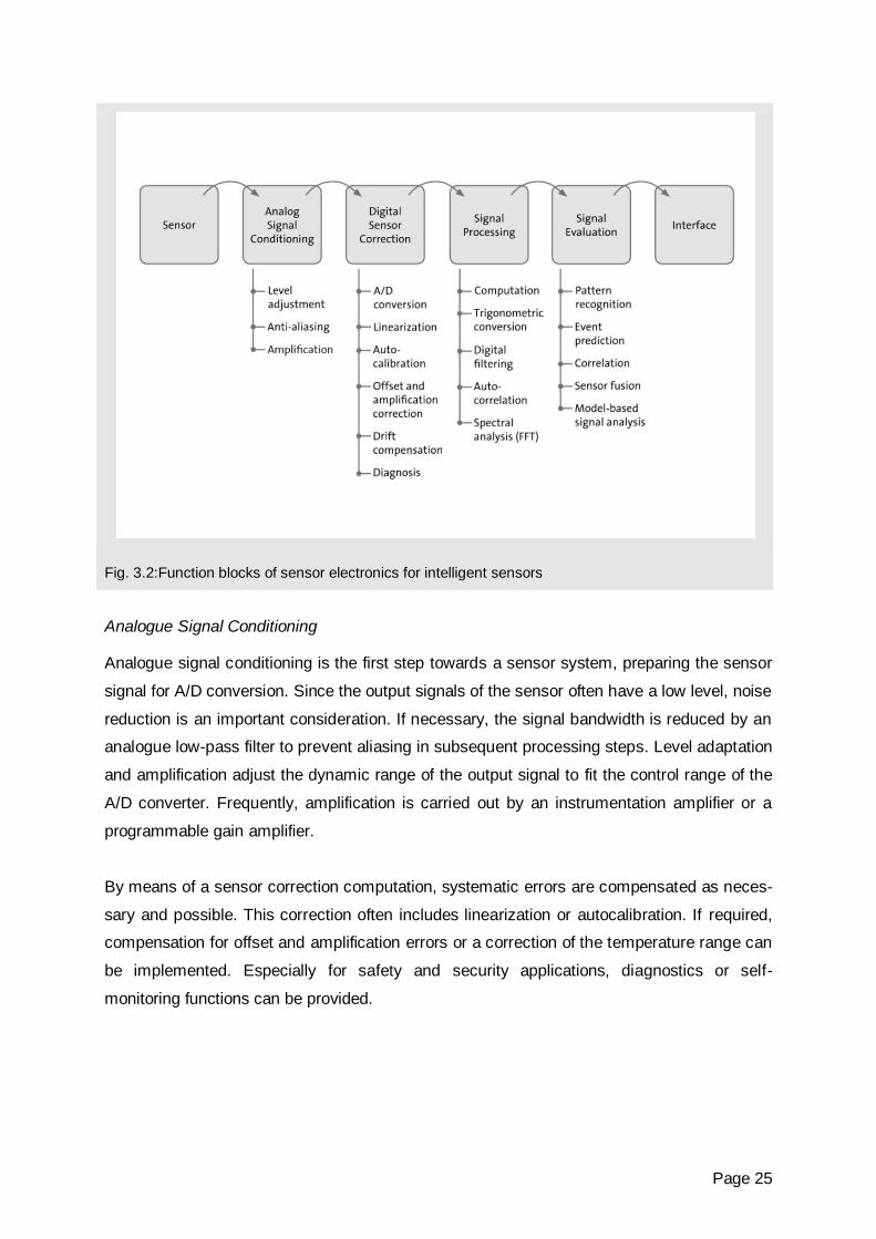
Fig. 3.2:Function blocks of sensor electronics for intelligent sensors
Analogue Signal Conditioning
Analogue signal conditioning is the first step towards a sensor system, preparing the sensor
signal for A/D conversion. Since the output signals of the sensor often have a low level, noise
reduction is an important consideration. If necessary, the signal bandwidth is reduced by an
analogue low-pass filter to prevent aliasing in subsequent processing steps. Level adaptation
and amplification adjust the dynamic range of the output signal to fit the control range of the
A/D converter. Frequently, amplification is carried out by an instrumentation amplifier or a
programmable gain amplifier.
By means of a sensor correction computation, systematic errors are compensated as neces-
sary and possible. This correction often includes linearization or autocalibration. If required,
compensation for offset and amplification errors or a correction of the temperature range can
be implemented. Especially for safety and security applications, diagnostics or self-
monitoring functions can be provided.
Page 26
Digital Signal Processing
The purpose of digital signal processing is to further improve the measuring signal (e.g. by
improve the signal-to-noise ratio, add digital filtering, or autocorrelation computation) or it is
used to derive secondary parameters from the raw data of the transducer. Examples can be
found for position sensors in which the computation of an angle is derived from the magnetic
field values or by the determination of typical frequency spectrums through FFT computation.
Intelligent sensors often not only transmit measurement values, but rather asses this value
and pass on the value of this assessment, in simple cases as an indication that an upper or
lower threshold was exceeded. By this means the bandwidth for complex systems as well as
the required processing capability of the superordinate levels can be reduced. A comparison
of the processed measuring signal with respective threshold values, complex patterns, or
model-based signatures follows. If necessary, the signals of further sensors are included at
this level for complex evaluations or confirmation of the results by plausibility checks.
Sensor interfaces often contain a serial digital bus interface, such as CAN, LIN, I2C, HART,
or SPI, or increasingly a wireless interface, such as ZigBee.
The demand of many users for improved maintainability of sensor systems is increasingly
being satisfied by storing sensor-specific correction data in a non-volatile memory. This al-
lows replacing individual sensors without recalibration. A standard data format is provided by
IEEE1451.
3.3 Implementation of Sensor-Signal Processing
Along with the further development of simple sensors into highly integrated sensor systems,
the following trends can be observed in the implementation of sensor-signal processing:
Reduced analogue signal conditioning, increased digital processing
As opposed to the classic analogue signal conditioning, digital signal processing offers con-
siderable advantages:
Greater stability, reliability, and reproducibility
Greater flexibility, easier implementation of variants, modifications, or extensions, as
well as adaptive evaluations

Page 27
Better cost degression
The importance of analogue signal conditioning is thus increasingly reduced to adapting the
output signal of the transducer to the input voltage range of the analogue-digital converter.
The requirements for resolution and speed of A/D converters is on the rise – signal process-
ing is in the digital domain. An example of signal filtering clearly shows the advantages:
While the implementation of small-band or adaptive analogue filters demands a considerable
effort for circuits and space requirements as well as compromises in the stability of the filter
characteristics, digital implementation is comparatively simple.
Use of Highly Integrated Components
Despite increasing functionality, component size, dissipation loss, and costs are nevertheless
required to remain low. Microcontrollers offer high functional density at low cost as well as a
high degree of flexibility. Highly integrated analogue or mixed-signal interface components
are also becoming increasingly available.
CMOS Analogue Circuits Instead of Bipolar Analogue Circuits
Better noise characteristics, lower power consumption for fast circuits and low offset values
are the basic upsides of bipolar technologies of high-grade analogue circuits. Nevertheless,
there is an obvious tendency towards CMOS-based sensor interface components. Thanks to
their advanced circuitry and technology performance, downsides can be compensated and
higher integration density utilized.
3.3.1 Components for Analogue Signal Conditioning
The data sheets of modern, powerful operational amplifiers reflect the advances made in
analogue CMOS circuit technology: high bandwidths, low noise, low supply voltage, low
power consumption, low space requirements thanks to small housing dimensions, and low
cost characterize many of the components found on today’s market. Based on special proc-
ess options for analogue performance, noise ratios with CMOS transistors attained 2.7
nV/Hz at 10 kHz and an extremely low power consumption of 1 µA.
Operational amplifiers today work with supply voltages of only 1.8 V, tending towards even
further reduction. Together with low power consumption, solutions for network independent
applications have become feasible.
Page 28
Parallel to this development, the functionality of sensor interface components is being ex-
tended. The ZMD21013, for instance, supports multiple sensors and is especially character-
ized by its low power consumption. During normal operation, the ZMD21013 only requires 25
to 30 µW. In standby mode, this value drops down to 1 µW. The MUSic family is optimized
for battery-operated mobile devices that operate with multiple sensors, controlled by micro-
controller.
3.3.2 Analogue-Digital Converters
The requirements for analogue-digital converters (ADCs) for sensor signal conditioning are
continuously being increased. A few years ago, resolutions of 8 or 10 bit were sufficient for
most applications; today, however, 12 to 14 bit and more are required.
In the area of sensor signal conditioning, successive approximation converters and increas-
ingly sigma-delta converters are being applied today.
These architectures are well suited for implementation in CMOS technology because they
have comparatively few analogue components. Thus they profit from technology scaling re-
garding reduced area, increased speed, and lower supply. Moreover, these architectures
allow the increased operating speeds of modern CMOS technologies for an increased sam-
pling rate, and increased resolution, i.e. accuracy.
Continued development of the technology and circuitry will enable a further increase in reso-
lution or accuracy of ADCs in sensor signal conditioning.
3.3.3 Microcontroller Units (MCUs) and Digital Signal Controllers (DSCs)
Many embedded sensor applications of today use microcontrollers for signal conditioning.
They are available in performance classes of up to 32 bits. For computation-intensive appli-
cations, DSCs can be used that provide fast real-time as well as computation-intensive proc-
essing for digital signal processing. MCUs and DSCs can be obtained with various numbers
of analogue inputs and ADCs. The resolution of the A/D converters is usually 10 or 12 bits,
often as successive approximation converters. Single MCUs, e.g. from Analog Devices, have
a 14-bit pipeline ADC e.g. TIs sigma-delta ADCs with resolutions of up to 24 bits. For net-
work-independent applications, practically all suppliers offer variants with low dissipation
loss. Moreover, MCUs and DSCs are available with a variety of bus interfaces (CAN, SPI
I2C, LIN, and increasingly wireless interfaces).
Page 29
This trend in MCUs and DSCs towards greater functionality and higher performance of the
analogue interfaces is expected to continue. Thus, they will continue to be an attractive alter-
native for intelligent sensors with comparatively low development effort and greater flexibility
at comparatively low cost. Due to the increasing availability of battery-operated or energy-
autonomous applications, reduced power dissipation per processing unit is still one of the
development objectives of many suppliers.
3.3.4 Field Programmable Gate Arrays (FPGAs)
FPGAs are a good alternative for processing digital sensor signals where the performance of
MCUs or DSCs is not sufficient or where only small quantities are required and subsequent
transition to an ASIC is planned. Based on a hardware description language (HDL), which is
also the basis for subsequent ASIC implementation, signal processing algorithms can be
verified and if necessary corrected (rapid prototyping).
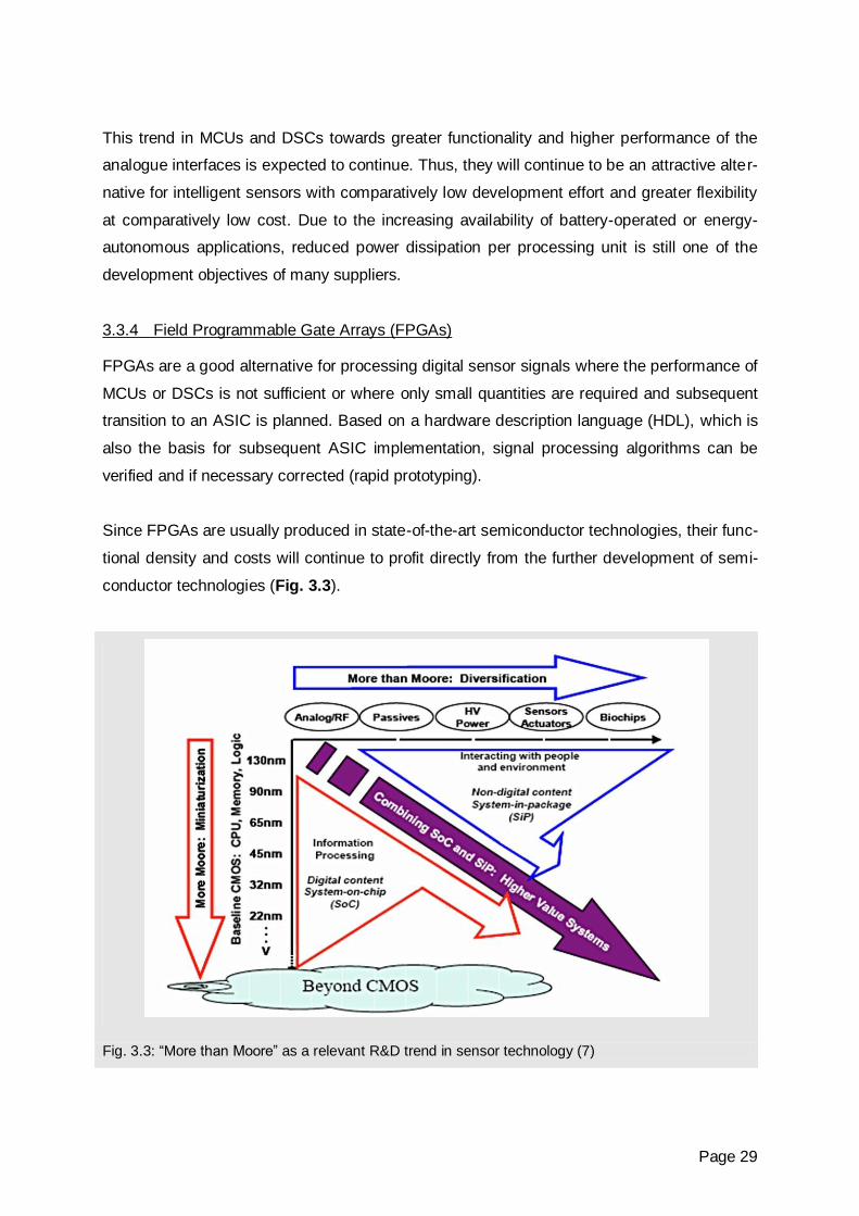
Since FPGAs are usually produced in state-of-the-art semiconductor technologies, their func-
tional density and costs will continue to profit directly from the further development of semi-
conductor technologies (Fig. 3.3).
Fig. 3.3: “More than Moore” as a relevant R&D trend in sensor technology (7)

Page 30
3.3.5 Application-Specific ICs (ASICs)
The development of ASICs is and will continue to be an alternative, whenever a sensor in
great quantities is concerned and/or low power dissipation, minimal form factors, and higher
copy protection are essential criteria in the choice of signal-conditioning implementation.
Modern ASIC technologies offer the capability to integrate analogue signal conditioning,
high-resolution A/D conversion, complex digital signal processing, sequence control, mem-
ory, and interface circuits in a single IC of very small dimensions and very low power dissipa-
tion. Inputs and outputs can be matched for performance and adjusted to the system specifi-
cations. Embedded MCUs, DSCs, or standard bus interfaces can be integrated in the design
as verified IPs.
The processing power can by far exceed that of MCUs and is adapted to the requirements.
In conjunction with appropriate power management, power dissipation can be minimized.
The integration density of modern semiconductor technologies, enables integration of multi-
ple ICs in to a single ASIC. By this means driver power can be reduced and space require-
ments, costs, and complexity of the circuitry can be minimized. The reliability is thus in-
creased, since the circuitry requires fewer connections.
The number of ASIC developments for sensor signal conditioning will drop in the next years,
because of increasing development costs due to increasing complexity on the one hand, and
on the other hand because of increasing performance and decreasing cost of microcontrol-
lers and FPGAs. Nevertheless, ASICs will remain viable wherever high quantities, high proc-
essing performance, and low dissipation losses at a low form factor are major requirements,
for instance in the area of embedded systems or in ambient intelligence.
3.4 Semiconductor Technology for IC Sensors
The greater part of all digital and mixed-signal ICs is produced today using CMOS tech-
niques. According to all predictions, the predominance of CMOS technology will continue for
at least the next ten years.
The roadmap for CMOS technology reflects the well-known Moore’s law since over 40 years.
Accordingly, the structure size in CMOS technologies is reduced every three years by a fac-
tor of ½. The development of high-volume standard products is also being carried out at pre-
Page 31
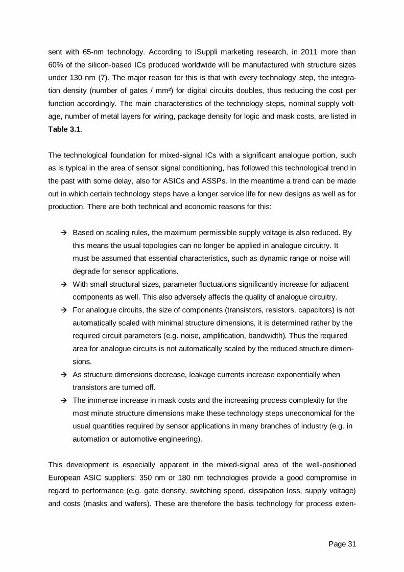
sent with 65-nm technology. According to iSuppli marketing research, in 2011 more than
60% of the silicon-based ICs produced worldwide will be manufactured with structure sizes
under 130 nm (7). The major reason for this is that with every technology step, the integra-
tion density (number of gates / mm²) for digital circuits doubles, thus reducing the cost per
function accordingly. The main characteristics of the technology steps, nominal supply volt-
age, number of metal layers for wiring, package density for logic and mask costs, are listed in
Table 3.1.
The technological foundation for mixed-signal ICs with a significant analogue portion, such
as is typical in the area of sensor signal conditioning, has followed this technological trend in
the past with some delay, also for ASICs and ASSPs. In the meantime a trend can be made
out in which certain technology steps have a longer service life for new designs as well as for
production. There are both technical and economic reasons for this:
Based on scaling rules, the maximum permissible supply voltage is also reduced. By
this means the usual topologies can no longer be applied in analogue circuitry. It
must be assumed that essential characteristics, such as dynamic range or noise will
degrade for sensor applications.
With small structural sizes, parameter fluctuations significantly increase for adjacent
components as well. This also adversely affects the quality of analogue circuitry.
For analogue circuits, the size of components (transistors, resistors, capacitors) is not
automatically scaled with minimal structure dimensions, it is determined rather by the
required circuit parameters (e.g. noise, amplification, bandwidth). Thus the required
area for analogue circuits is not automatically scaled by the reduced structure dimen-
sions.
As structure dimensions decrease, leakage currents increase exponentially when
transistors are turned off.
The immense increase in mask costs and the increasing process complexity for the
most minute structure dimensions make these technology steps uneconomical for the
usual quantities required by sensor applications in many branches of industry (e.g. in
automation or automotive engineering).
This development is especially apparent in the mixed-signal area of the well-positioned
European ASIC suppliers: 350 nm or 180 nm technologies provide a good compromise in
regard to performance (e.g. gate density, switching speed, dissipation loss, supply voltage)
and costs (masks and wafers). These are therefore the basis technology for process exten-
Page 32
sions, such as high-voltage or RF options, non-volatile memories, special devices, which
make them interesting for sensor applications.
Table 3.1: Characteristics of CMOS Technology Nodes
Process
(µm)
VDD
[V]
Metal Gates
per mm2
Mask Set Cost
[US $]
0.065 1.0 9 400k 3,000,000
0.09 1.0 9 200k 1,500,000
0.13 1.2 7 100k 750,000
0.18 1.8 5 40k 250,000
0.25 2.5 5 24k 150,000
0.35 3.3 3 12k 40,000
0.5 3.3 3 5k 20,000
0.6 5.0 2 4k 18,000
Notes:
Process (µm): Process nodes as per ITRS roadmap
VDD: Standard supply voltage
Metal: Maximal number of circuit layers
Gate/mm²: Benchmark for number of gates per mm²
Mask Set Cost: Reference value for the cost of a mask set in US$
This trend is also reflected by future exploratory research in the field of micro and nano-
electronics in Germany and Europe in general: A major objective of the R&D activities is the
expansion of existing digital semiconductor technologies towards platforms for the develop-
ment of heterogeneous systems (Fig. 3.3).
3.5 High Temperature Electronics
Especially in automotive engineering, the requirements for the reliability of sensors and sil i-
con-based sensor signal conditioning are increasing. Ten years ago, sensors/actuators and
control devices in vehicles were still spatially separated. Even for applications in the engine,
a maximum ambient temperature of 150 °C was thus sufficient for signal conditioning. The
spatial bundling of sensor/actuator technology leads to today’s requirement of a maximum
ambient temperature of 175 °C. The trend towards system integration of electronics and sen-
sors/actuators also leads to further increases of the required ambient temperature. In a few
years, the requirement will be at 210 °C. Semiconductor suppliers are increasingly accom-
Page 33
modating this trend: More and more manufacturers are qualifying their silicon processes and
libraries according to the requirements of automobile makers. There are already a number of
makers, who are specifying a maximum ambient temperature of 150 °C or even 170 °C with
a temperature profile, specifying 1,000 hours for instance at the maximum temperature (8).
3.6 Self-Monitoring and Reconfiguration
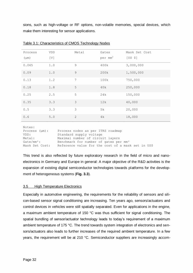
The more “intelligence” integrated in a sensor in form of sophisticated signal processing algo-
rithms, the greater the possibilities of self-monitoring and reconfiguration. Self-monitoring of
sensors refers to fault (disturbance) detection and interference (noise) diagnosis (9), (10).
With the aid of such monitoring processes, sensor reliability, i.e. knowledge of their operating
status, increases (Fig. 3.4).
Fig. 3.4: Parameters affecting the increase of reliability as the main objective of sensor self-monitoring (12)
On the other hand, the additional processes for self-monitoring, which also have a limited
reliability, effectively reduce the overall reliability of autonomous sensors. Therefore, one of
the future aims is to compensate this reduced reliability by adding redundancies in the sen-
sor (10).
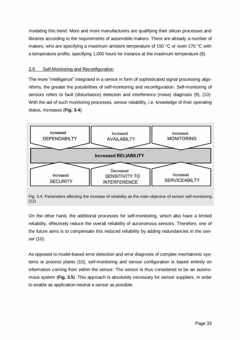
As opposed to model-based error detection and error diagnosis of complex mechatronic sys-
tems or process plants (10), self-monitoring and sensor configuration is based entirely on
information coming from within the sensor. The sensor is thus considered to be an autono-
mous system (Fig. 3.5). This approach is absolutely necessary for sensor suppliers, in order
to enable as application-neutral a sensor as possible.
Page 34
In contrast to error detection and error diagnosis in mechatronic systems, sensor technology
refers to disturbances, since the term “error” has, since Gauss, a different meaning: In
measuring technology every sensor has permissible errors – uncertainties of measurement.
The method of process coupling requires external data for self-monitoring that do not origi-
nate from the sensor itself. In its more basic form this might rely on data exchange between
nearby sensors and actuators with subsequent comparison and plausibility checks. More
advanced forms of process coupling incorporate computations based on process models. By
means of available parameters in the model, such as the measuring signal or actuating vari-
ables, the output parameters to be monitored can be computed. Of course these methods
require comprehensive knowledge of the process behaviour.
Only the user has knowledge about the process involved and only he can thus subsequently
implement the monitoring algorithm. Model-based processes are at the focus of error detec-
tion and diagnosis of mechatronic systems (10). The high development costs required here
are borne by the quantities of the systems, e.g. in automotive engineering.
Fig. 3.5: Classification of sensor self-monitoring methods and processes (12)
Page 35
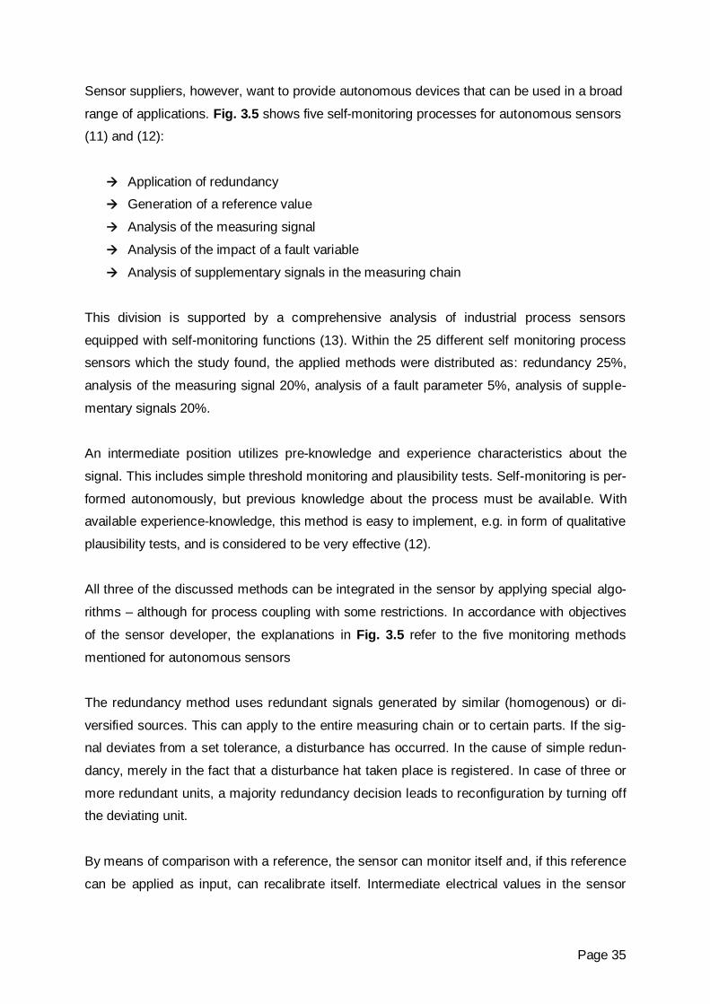
Sensor suppliers, however, want to provide autonomous devices that can be used in a broad
range of applications. Fig. 3.5 shows five self-monitoring processes for autonomous sensors
(11) and (12):
Application of redundancy
Generation of a reference value
Analysis of the measuring signal
Analysis of the impact of a fault variable
Analysis of supplementary signals in the measuring chain
This division is supported by a comprehensive analysis of industrial process sensors
equipped with self-monitoring functions (13). Within the 25 different self monitoring process
sensors which the study found, the applied methods were distributed as: redundancy 25%,
analysis of the measuring signal 20%, analysis of a fault parameter 5%, analysis of supple-
mentary signals 20%.
An intermediate position utilizes pre-knowledge and experience characteristics about the
signal. This includes simple threshold monitoring and plausibility tests. Self-monitoring is per-
formed autonomously, but previous knowledge about the process must be available. With
available experience-knowledge, this method is easy to implement, e.g. in form of qualitative
plausibility tests, and is considered to be very effective (12).
All three of the discussed methods can be integrated in the sensor by applying special algo-
rithms – although for process coupling with some restrictions. In accordance with objectives
of the sensor developer, the explanations in Fig. 3.5 refer to the five monitoring methods
mentioned for autonomous sensors
The redundancy method uses redundant signals generated by similar (homogenous) or di-
versified sources. This can apply to the entire measuring chain or to certain parts. If the sig-
nal deviates from a set tolerance, a disturbance has occurred. In the cause of simple redun-
dancy, merely in the fact that a disturbance hat taken place is registered. In case of three or
more redundant units, a majority redundancy decision leads to reconfiguration by turning off
the deviating unit.
By means of comparison with a reference, the sensor can monitor itself and, if this reference
can be applied as input, can recalibrate itself. Intermediate electrical values in the sensor
Page 36
measuring chain can also be referenced. In this case, monitoring is restricted to the subse-
quent signal processing blocks.
To analyze the measuring signal, sensor-specific threshold values and trends are monitored.
These values are derived from the specific operating conditions of the respective sensor
group. A further monitoring possibility is offered by additional information contained in the
measuring signal, e.g. higher frequency components in semi-static measurements.
Analysis of disturbance requires evaluating how the undesired, but known effect of the sensi-
tivity to disturbance (cross-sensitivity) affects the various transfer blocks of the measuring
chain. This is achieved by detecting the disturbance parameter in a separate measuring
channel. Subsequent comparison with the intermediate signals of the disturbed measuring
chain, allows identifying, diagnosing and possibly compensating the disturbance.
Supplementary sensor-internal signals or supplementary parameters can be used to deter-
mine the actual state of a sensor. This involves signals and parameters that are not transmit-
ted along with the measuring signal, e.g. the supply voltage of measuring bridges, and their
resistance parameters. These methods are primarily applied to monitor the sensor electron-
ics (self-testing) and are concentrated on especially vulnerable assemblies and components.
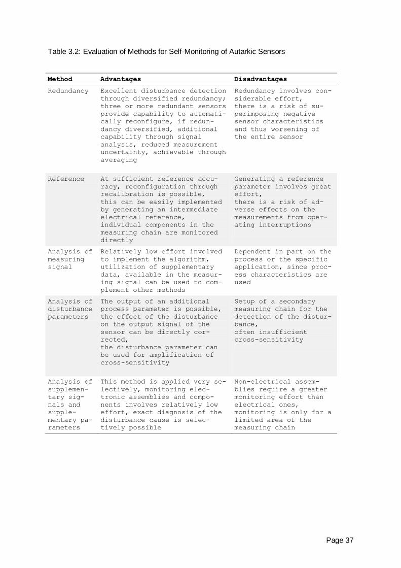
An evaluation of the monitoring methods in (12) and (14) results in the advantages and dis-
advantages listed in Table 3.2.
Progress in sensor self-monitoring is especially being made in the area of complex signal
processing in autonomous sensors. Main focus is methods that analyze the measuring signal
and the cross-sensitivities to disturbances. However, combinations of various methods and
the implementation of known characteristics of the main application areas also seems prom-
ising.
The possibilities of sensor reconfiguration are being increasingly explored. A major contribu-
tion in this area could come from micro-electromechanical silicon sensors (MEMS sensors)
that can be implemented in low-cost arrays to provide the required redundancy. Other ap-
proaches are automatic recalibration or specific reduction of sensor functionality and accu-
racy, i.e. degradation strategies.
Page 37
Table 3.2: Evaluation of Methods for Self-Monitoring of Autarkic Sensors
Method Advantages Disadvantages
Redundancy Excellent disturbance detection
through diversified redundancy;
three or more redundant sensors
provide capability to automati-
cally reconfigure, if redun-
dancy diversified, additional
capability through signal
analysis, reduced measurement
uncertainty, achievable through
averaging
Redundancy involves con-
siderable effort,
there is a risk of su-
perimposing negative
sensor characteristics
and thus worsening of
the entire sensor
Reference At sufficient reference accu-
racy, reconfiguration through
recalibration is possible,
this can be easily implemented
by generating an intermediate
electrical reference,
individual components in the
measuring chain are monitored
directly
Generating a reference
parameter involves great
effort,
there is a risk of ad-
verse effects on the
measurements from oper-
ating interruptions
Analysis of
measuring
signal
Relatively low effort involved
to implement the algorithm,
utilization of supplementary
data, available in the measur-
ing signal can be used to com-
plement other methods
Dependent in part on the
process or the specific
application, since proc-
ess characteristics are
used
Analysis of
disturbance
parameters
The output of an additional
process parameter is possible,
the effect of the disturbance
on the output signal of the
sensor can be directly cor-
rected,
the disturbance parameter can
be used for amplification of
cross-sensitivity
Setup of a secondary
measuring chain for the
detection of the distur-
bance,
often insufficient
cross-sensitivity
Analysis of
supplemen-
tary sig-
nals and
supple-
mentary pa-
rameters
This method is applied very se-
lectively, monitoring elec-
tronic assemblies and compo-
nents involves relatively low
effort, exact diagnosis of the
disturbance cause is selec-
tively possible
Non-electrical assem-
blies require a greater
monitoring effort than
electrical ones,
monitoring is only for a
limited area of the
measuring chain
Page 38
4 Development Trends –
Communication and System Integration
Abstract
Driven by increasing quantities and increasing price pressure, many sensor suppliers are
moving their creation of value more and more to signal processing, energy management,
self-monitoring, and miniaturization. Overall, the cost of ownership is diminishing. The major
trends are:
Digital interfaces
More wireless sensor technology
Processing of measurement values
Parallel detection of multiple measuring values
Autonomous sensor systems
Miniaturized sensor networks (smart dust)
Self-diagnosis and auto-calibration
__________
A major challenge for sensor technology lies in continuously reducing of constructive efforts
required from the application. Besides standardized connectors, this leads to increasingly
miniaturized designs, more decentralized signal processing and asynchronous transmission
of threshold and disturbance values, instead of the continuous transmission of measured
data. Energy management and self-monitoring are also becoming increasingly sophisticated.
Sensors are thereby increasingly being hierarchically networked in hierarchies and the com-
plexity of sensor applications continues to increase along with the technical capacities.
4.1 Wire-Bound Interfaces
Digital interfaces are prevailing more and more, although application-specific interfaces con-
tinue to have their place (Fig. 4.2). At present, the significant interfaces are:
Digital: CAN automotive, EIB/LON, field bus, Profibus, Ethernet, AS interface,
FlexRay, I/O Link
Analogue: two-wire, 4-20 mA
Page 39
4.2 Wireless Sensor Technology
Wireless sensing is a new, very promising field in sensor technology. Wireless transmission
of measuring data is by no means a novelty, but its potential has only recently become ap-
parent for the industry, commerce, and end-user sectors. A significant number of market par-
ticipants and applications fragments these sectors. The alluring benefits however bring with
them a number of challenges, so that its implementation has progressed slowly up to now.
In the meantime though, continuous developments in this area have overcome many of the
disadvantages posed by this new technology, such as a lack of reliability. It is expected that
wireless sensing will be accepted by the end users. Through this route it will also find its way
into other areas, proving its ability to solve real application problems that by conventional
means cannot be solved at all or only with great difficulty. Some sensor companies have al-
ready started working in these areas. Thus, wireless sensor technology will open new oppor-
tunities (16).
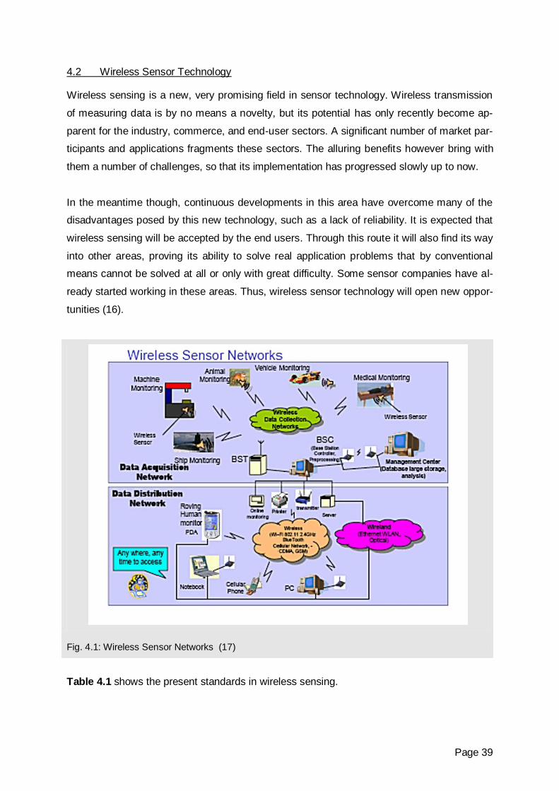
Fig. 4.1: Wireless Sensor Networks (17)
Table 4.1 shows the present standards in wireless sensing.
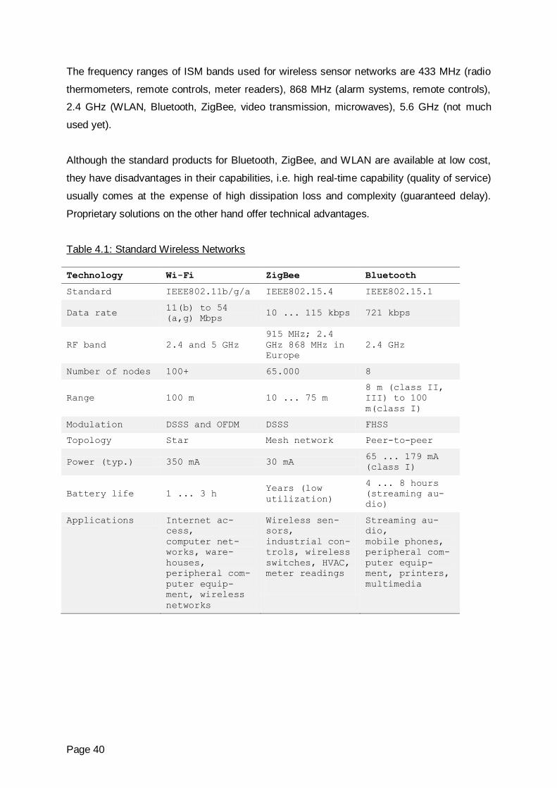
Page 40
The frequency ranges of ISM bands used for wireless sensor networks are 433 MHz (radio
thermometers, remote controls, meter readers), 868 MHz (alarm systems, remote controls),
2.4 GHz (WLAN, Bluetooth, ZigBee, video transmission, microwaves), 5.6 GHz (not much
used yet).
Although the standard products for Bluetooth, ZigBee, and WLAN are available at low cost,
they have disadvantages in their capabilities, i.e. high real-time capability (quality of service)
usually comes at the expense of high dissipation loss and complexity (guaranteed delay).
Proprietary solutions on the other hand offer technical advantages.
Table 4.1: Standard Wireless Networks
Technology Wi-Fi ZigBee Bluetooth
Standard IEEE802.11b/g/a IEEE802.15.4 IEEE802.15.1
Data rate 11(b) to 54
(a,g) Mbps 10 ... 115 kbps 721 kbps
RF band 2.4 and 5 GHz
915 MHz; 2.4
GHz 868 MHz in
Europe
2.4 GHz
Number of nodes 100+ 65.000 8
Range 100 m 10 ... 75 m
8 m (class II,
III) to 100
m(class I)
Modulation DSSS and OFDM DSSS FHSS
Topology Star Mesh network Peer-to-peer
Power (typ.) 350 mA 30 mA 65 ... 179 mA
(class I)
Battery life 1 ... 3 h Years (low
utilization)
4 ... 8 hours
(streaming au-
dio)
Applications Internet ac-
cess,
computer net-
works, ware-
houses,
peripheral com-
puter equip-
ment, wireless
networks
Wireless sen-
sors,
industrial con-
trols, wireless
switches, HVAC,
meter readings
Streaming au-
dio,
mobile phones,
peripheral com-
puter equip-
ment, printers,
multimedia
Page 41
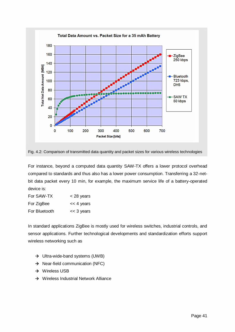
Fig. 4.2: Comparison of transmitted data quantity and packet sizes for various wireless technologies
For instance, beyond a computed data quantity SAW-TX offers a lower protocol overhead
compared to standards and thus also has a lower power consumption. Transferring a 32-net-
bit data packet every 10 min, for example, the maximum service life of a battery-operated
device is:
For SAW-TX < 28 years
For ZigBee << 4 years
For Bluetooth << 3 years
In standard applications ZigBee is mostly used for wireless switches, industrial controls, and
sensor applications. Further technological developments and standardization efforts support
wireless networking such as
Ultra-wide-band systems (UWB)
Near-field communication (NFC)
Wireless USB
Wireless Industrial Network Alliance
Page 42
Embedding sensor networks in available communication networks, gives added significance
to the categories space and time which thus need to be addressed accordingly. Often it is of
interest where and when a physical event has taken place. Also, the complex interplay be-
tween the data from different sensor nodes requires a spatial and temporal reference sys-
tem. Therefore suitable mechanisms for localizing and synchronizing the nodes in a sensor
network have become necessary. Additionally, integration of sensor networks into existing
infrastructures and connecting to the Internet are often needed, for instance to allow world-
wide access to a sensor network or to enable sensor networks to make use of Internet-based
services and resources. Protocols, such as IEEE 802.15.4 or 6LowPAN (IPv6 over low-
power wireless personal area networks) function as bridges to low-cost links to the Internet.
4.3 Motes and Smart Dust
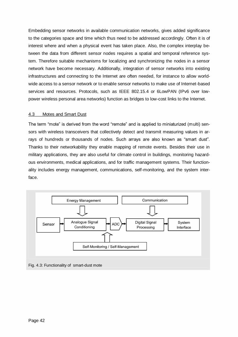
The term “mote” is derived from the word “remote” and is applied to miniaturized (multi) sen-
sors with wireless transceivers that collectively detect and transmit measuring values in ar-
rays of hundreds or thousands of nodes. Such arrays are also known as “smart dust”.
Thanks to their networkability they enable mapping of remote events. Besides their use in
military applications, they are also useful for climate control in buildings, monitoring hazard-
ous environments, medical applications, and for traffic management systems. Their function-
ality includes energy management, communications, self-monitoring, and the system inter-
face.
Fig. 4.3: Functionality of smart-dust mote
Page 43
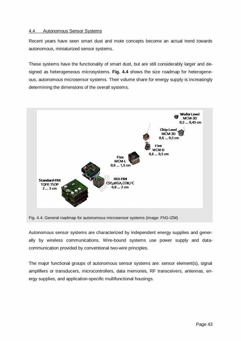
4.4 Autonomous Sensor Systems
Recent years have seen smart dust and mote concepts become an actual trend towards
autonomous, miniaturized sensor systems.
These systems have the functionality of smart dust, but are still considerably larger and de-
signed as heterogeneous microsystems. Fig. 4.4 shows the size roadmap for heterogene-
ous, autonomous microsensor systems. Their volume share for energy supply is increasingly
determining the dimensions of the overall systems.
Fig. 4.4: General roadmap for autonomous microsensor systems (image: FhG-IZM)
Autonomous sensor systems are characterized by independent energy supplies and gener-
ally by wireless communications. Wire-bound systems use power supply and data-
communication provided by conventional two-wire principles.
The major functional groups of autonomous sensor systems are: sensor element(s), signal
amplifiers or transducers, microcontrollers, data memories, RF transceivers, antennas, en-
ergy supplies, and application-specific multifunctional housings.
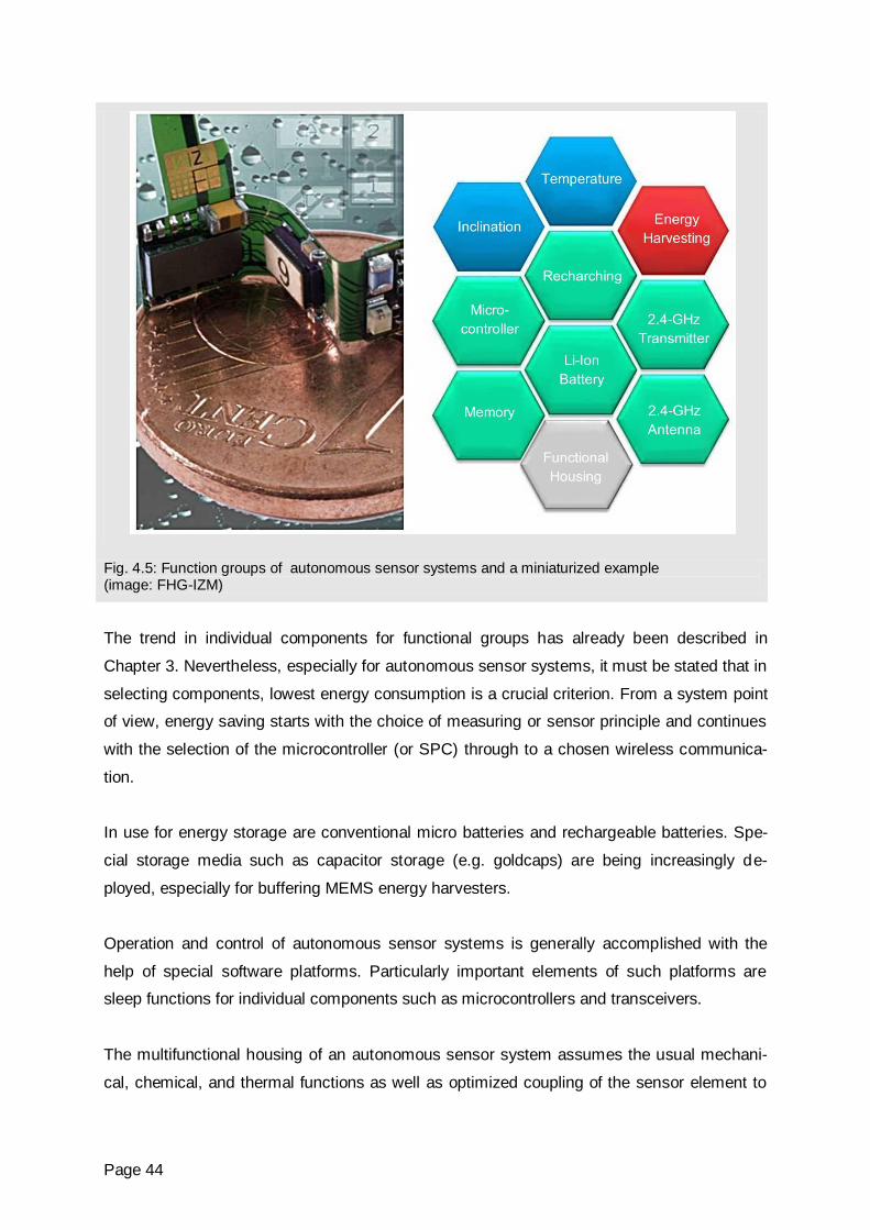
Page 44
Fig. 4.5: Function groups of autonomous sensor systems and a miniaturized example (image: FHG-IZM)
The trend in individual components for functional groups has already been described in
Chapter 3. Nevertheless, especially for autonomous sensor systems, it must be stated that in
selecting components, lowest energy consumption is a crucial criterion. From a system point
of view, energy saving starts with the choice of measuring or sensor principle and continues
with the selection of the microcontroller (or SPC) through to a chosen wireless communica-
tion.
In use for energy storage are conventional micro batteries and rechargeable batteries. Spe-
cial storage media such as capacitor storage (e.g. goldcaps) are being increasingly de-
ployed, especially for buffering MEMS energy harvesters.
Operation and control of autonomous sensor systems is generally accomplished with the
help of special software platforms. Particularly important elements of such platforms are
sleep functions for individual components such as microcontrollers and transceivers.
The multifunctional housing of an autonomous sensor system assumes the usual mechani-
cal, chemical, and thermal functions as well as optimized coupling of the sensor element to
Page 45
the environment. It is often equipped with a visual function display and microswitches or in-
terfaces for reset and programming functions.
Autonomous sensor systems make use of established production technologies and are sub-
ject to their trends. Nevertheless, 3D structure technologies, such as stacking and folding of
flex substrates is applied, as illustrated in the example in Fig. 4.5.
Some autonomous sensor systems are equipped with software that enable autonomous
sensor network generation. Besides proprietary programs, open-source software can already
be found on the Internet. The market leaders in automation technology now offer receiving
devices with which sensor data from autonomous sensors can be read into conventional
communication structures.
Some Applications
In logistics there is a trend to include sensor functions (e.g. temperature, acceleration, GPS)
on tags. Such autonomous sensor systems are often referred to as active transponders.
In the food industry, tracking and documentation systems are being developed or designed
based on autonomous sensor systems – electronic labels with sensor functions.
In the field of animal protection (livestock, fish, birds) or animal food production, first autono-
mous sensor systems are starting to be implemented commercially, to identify animal behav-
iour. The trend here is to use such sensor systems to monitor the health of the livestock and
thus to prevent diseases and contagion at an early stage.
Discussions are being held on the implementation of autonomous sensor systems for condi-
tion monitoring in the investment goods industry. First example applications that complement
existing systems in process technology are known to be implemented.
It is estimated generally that the application of autonomous sensor systems in consumer
goods (e.g. radio weather stations) has started and that other fields and areas of application
will be identified and developed.
In the power industry, first applications in overhead line monitoring with autonomous sensor
systems are in the trial phase.
Page 46
5 Development Trends –
Packaging
Abstract
Packaging costs are a major factor in sensor production. Therefore, besides improvement of
robustness, the focus is on cost reduction.
In the context of greater application-specific products, the following trends can be observed
in packaging:
Increase of stacked ICs
Increasing flip-chip assembly
Hermetic housings
Integrated functions in carriers and substrates
3D packages with integrated function elements
More effective mechanical decoupling of sensor elements and housings
Novel integration concepts (textile, lab-on-chip, lab-on-disk, passivated medical in-
vivo systems, etc.)
__________
Generally, in the area of housing and packaging there is a trend towards specialization cor-
responding to the technical requirements. Sensor suppliers are working to reduce the effects
of mechanical stress on measurements, because this plays an increasingly important role in
reducing measuring uncertainty, due to its non-reproducibility. Existing assembly and hous-
ing materials are being improved and new ones are being developed. In medical technology
a tremendous R&D effort has been started for new sensor-actuator systems for in-vivo appli-
cations, both temporary and permanent. The effort to develop “smart” clothes is also being
increased considerably.
Packaging in the sensor industry is divided into various hierarchical levels. There is 1st level
packaging for the sensor element, 2nd level packaging, which integrates components and
substrates in an assembly, and then the overall system level, i.e. of the device or a mecha-
tronic unit (Fig. 5.1).
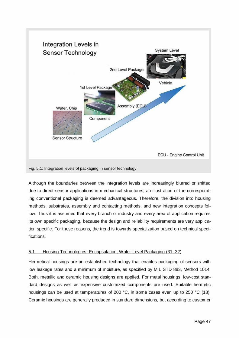
Page 47
Fig. 5.1: Integration levels of packaging in sensor technology
Although the boundaries between the integration levels are increasingly blurred or shifted
due to direct sensor applications in mechanical structures, an illustration of the correspond-
ing conventional packaging is deemed advantageous. Therefore, the division into housing
methods, substrates, assembly and contacting methods, and new integration concepts fol-
low. Thus it is assumed that every branch of industry and every area of application requires
its own specific packaging, because the design and reliability requirements are very applica-
tion specific. For these reasons, the trend is towards specialization based on technical speci-
fications.
5.1 Housing Technologies, Encapsulation, Wafer-Level Packaging (31, 32)
Hermetical housings are an established technology that enables packaging of sensors with
low leakage rates and a minimum of moisture, as specified by MIL STD 883, Method 1014.
Both, metallic and ceramic housing designs are applied. For metal housings, low-cost stan-
dard designs as well as expensive customized components are used. Suitable hermetic
housings can be used at temperatures of 200 °C, in some cases even up to 250 °C (18).
Ceramic housings are generally produced in standard dimensions, but according to customer
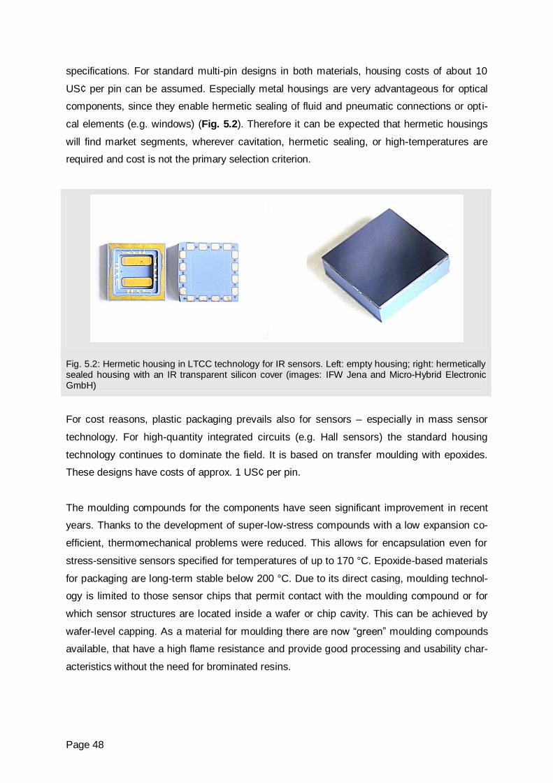
Page 48
specifications. For standard multi-pin designs in both materials, housing costs of about 10
US¢ per pin can be assumed. Especially metal housings are very advantageous for optical
components, since they enable hermetic sealing of fluid and pneumatic connections or opti-
cal elements (e.g. windows) (Fig. 5.2). Therefore it can be expected that hermetic housings
will find market segments, wherever cavitation, hermetic sealing, or high-temperatures are
required and cost is not the primary selection criterion.
Fig. 5.2: Hermetic housing in LTCC technology for IR sensors. Left: empty housing; right: hermetically sealed housing with an IR transparent silicon cover (images: IFW Jena and Micro-Hybrid Electronic GmbH)
For cost reasons, plastic packaging prevails also for sensors – especially in mass sensor
technology. For high-quantity integrated circuits (e.g. Hall sensors) the standard housing
technology continues to dominate the field. It is based on transfer moulding with epoxides.
These designs have costs of approx. 1 US¢ per pin.
The moulding compounds for the components have seen significant improvement in recent
years. Thanks to the development of super-low-stress compounds with a low expansion co-
efficient, thermomechanical problems were reduced. This allows for encapsulation even for
stress-sensitive sensors specified for temperatures of up to 170 °C. Epoxide-based materials
for packaging are long-term stable below 200 °C. Due to its direct casing, moulding technol-
ogy is limited to those sensor chips that permit contact with the moulding compound or for
which sensor structures are located inside a wafer or chip cavity. This can be achieved by
wafer-level capping. As a material for moulding there are now “green” moulding compounds
available, that have a high flame resistance and provide good processing and usability char-
acteristics without the need for brominated resins.
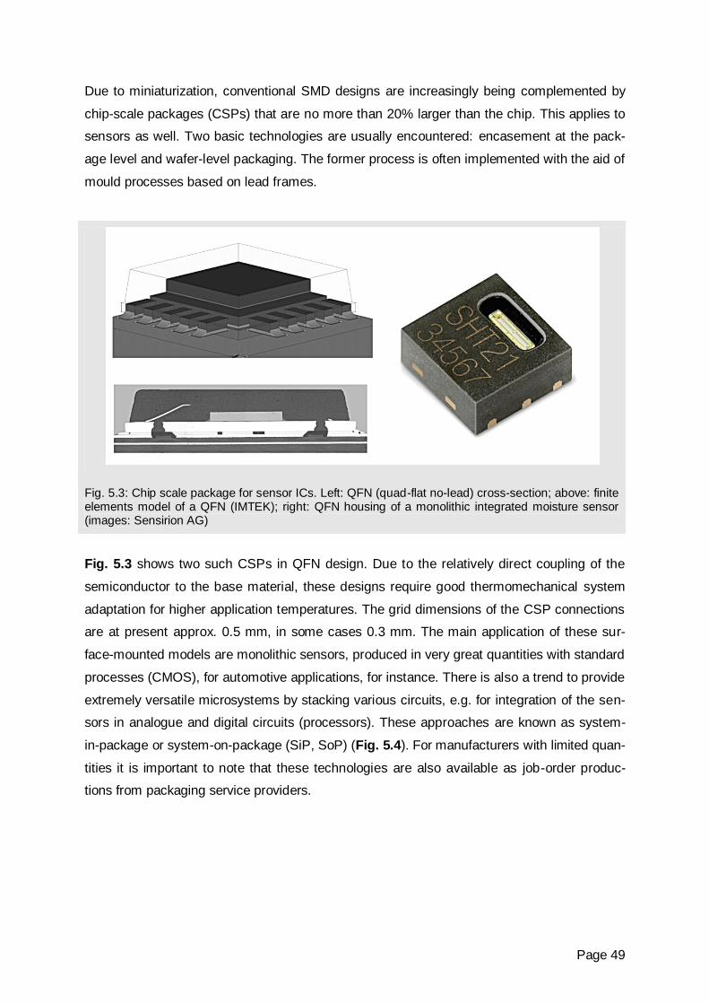
Page 49
Due to miniaturization, conventional SMD designs are increasingly being complemented by
chip-scale packages (CSPs) that are no more than 20% larger than the chip. This applies to
sensors as well. Two basic technologies are usually encountered: encasement at the pack-
age level and wafer-level packaging. The former process is often implemented with the aid of
mould processes based on lead frames.
Fig. 5.3 shows two such CSPs in QFN design. Due to the relatively direct coupling of the
semiconductor to the base material, these designs require good thermomechanical system
adaptation for higher application temperatures. The grid dimensions of the CSP connections
are at present approx. 0.5 mm, in some cases 0.3 mm. The main application of these sur-
face-mounted models are monolithic sensors, produced in very great quantities with standard
processes (CMOS), for automotive applications, for instance. There is also a trend to provide
extremely versatile microsystems by stacking various circuits, e.g. for integration of the sen-
sors in analogue and digital circuits (processors). These approaches are known as system-
in-package or system-on-package (SiP, SoP) (Fig. 5.4). For manufacturers with limited quan-
tities it is important to note that these technologies are also available as job-order produc-
tions from packaging service providers.
Fig. 5.3: Chip scale package for sensor ICs. Left: QFN (quad-flat no-lead) cross-section; above: finite elements model of a QFN (IMTEK); right: QFN housing of a monolithic integrated moisture sensor (images: Sensirion AG)
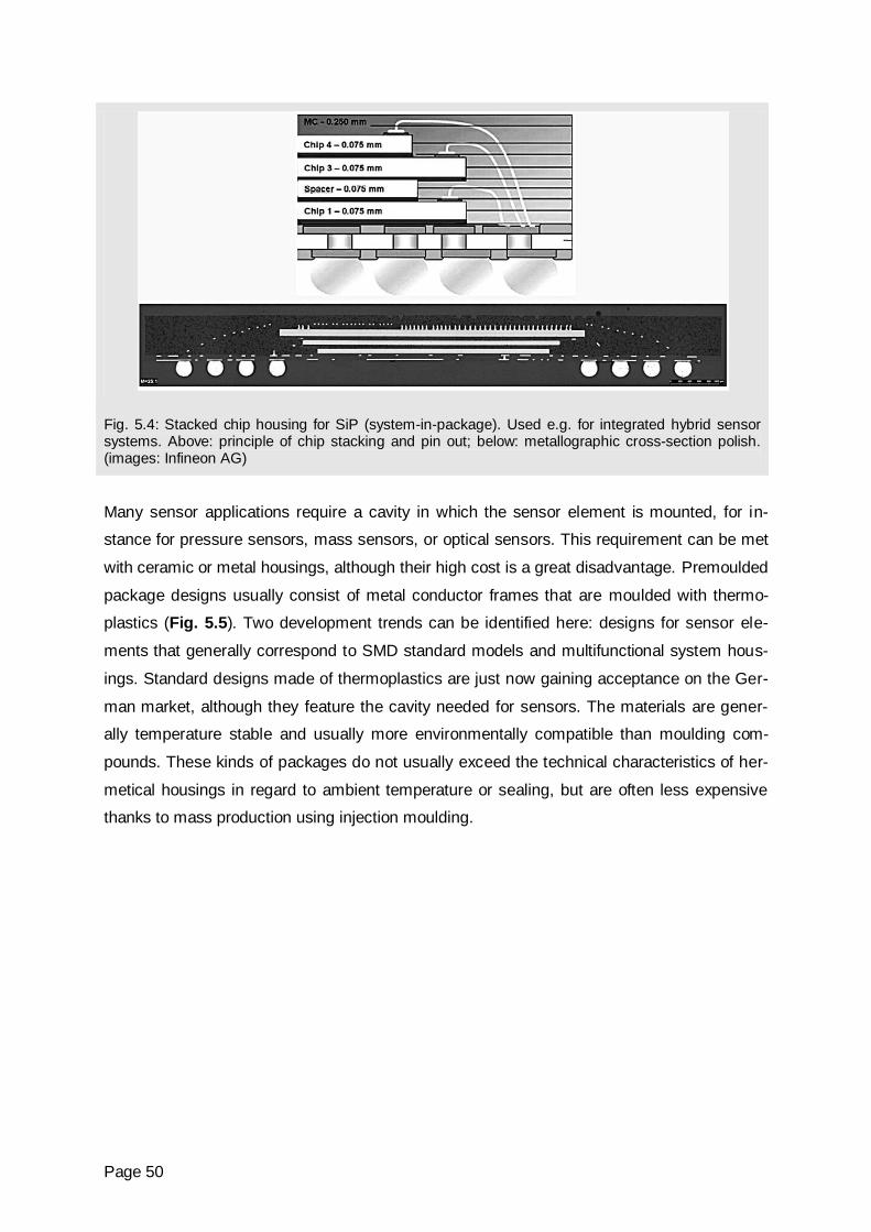
Page 50
Fig. 5.4: Stacked chip housing for SiP (system-in-package). Used e.g. for integrated hybrid sensor systems. Above: principle of chip stacking and pin out; below: metallographic cross-section polish. (images: Infineon AG)
Many sensor applications require a cavity in which the sensor element is mounted, for in-
stance for pressure sensors, mass sensors, or optical sensors. This requirement can be met
with ceramic or metal housings, although their high cost is a great disadvantage. Premoulded
package designs usually consist of metal conductor frames that are moulded with thermo-
plastics (Fig. 5.5). Two development trends can be identified here: designs for sensor ele-
ments that generally correspond to SMD standard models and multifunctional system hous-
ings. Standard designs made of thermoplastics are just now gaining acceptance on the Ger-
man market, although they feature the cavity needed for sensors. The materials are gener-
ally temperature stable and usually more environmentally compatible than moulding com-
pounds. These kinds of packages do not usually exceed the technical characteristics of her-
metical housings in regard to ambient temperature or sealing, but are often less expensive
thanks to mass production using injection moulding.
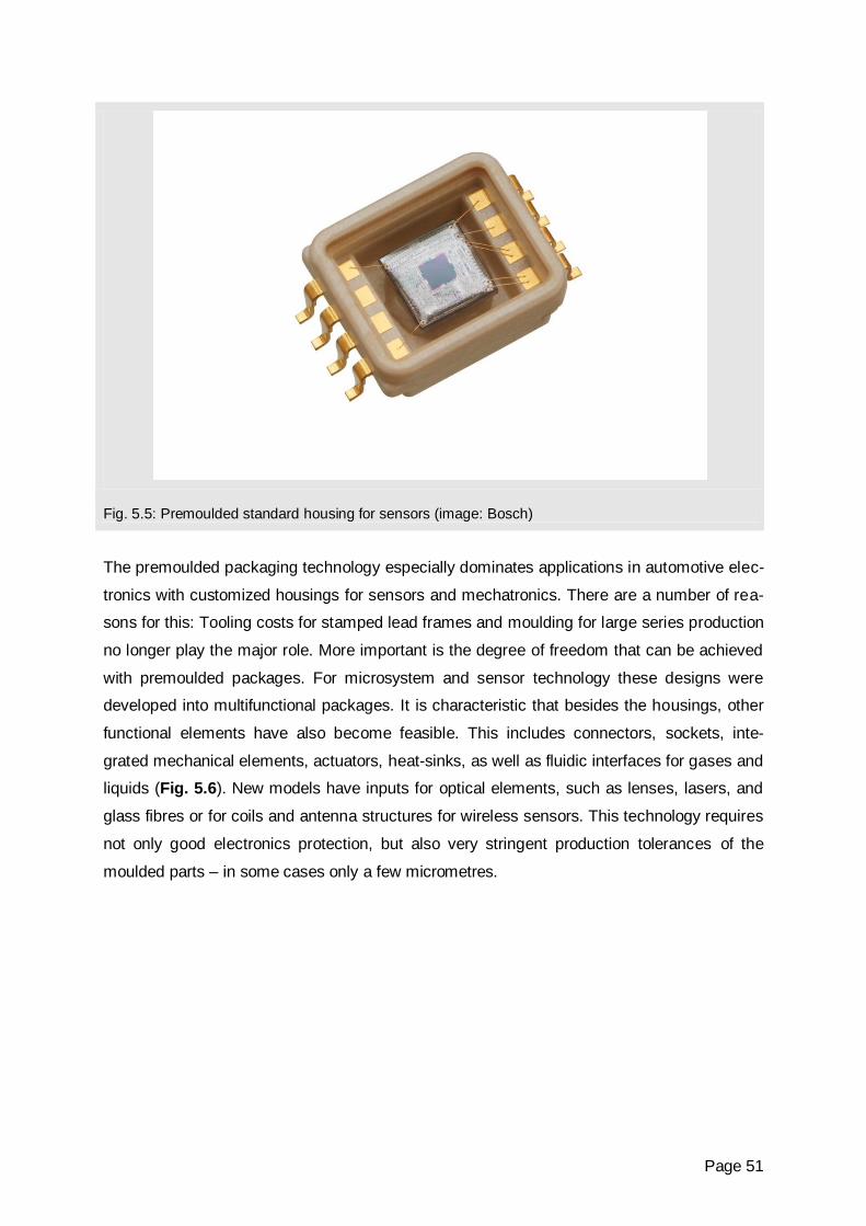
Page 51
Fig. 5.5: Premoulded standard housing for sensors (image: Bosch)
The premoulded packaging technology especially dominates applications in automotive elec-
tronics with customized housings for sensors and mechatronics. There are a number of rea-
sons for this: Tooling costs for stamped lead frames and moulding for large series production
no longer play the major role. More important is the degree of freedom that can be achieved
with premoulded packages. For microsystem and sensor technology these designs were
developed into multifunctional packages. It is characteristic that besides the housings, other
functional elements have also become feasible. This includes connectors, sockets, inte-
grated mechanical elements, actuators, heat-sinks, as well as fluidic interfaces for gases and
liquids (Fig. 5.6). New models have inputs for optical elements, such as lenses, lasers, and
glass fibres or for coils and antenna structures for wireless sensors. This technology requires
not only good electronics protection, but also very stringent production tolerances of the
moulded parts – in some cases only a few micrometres.
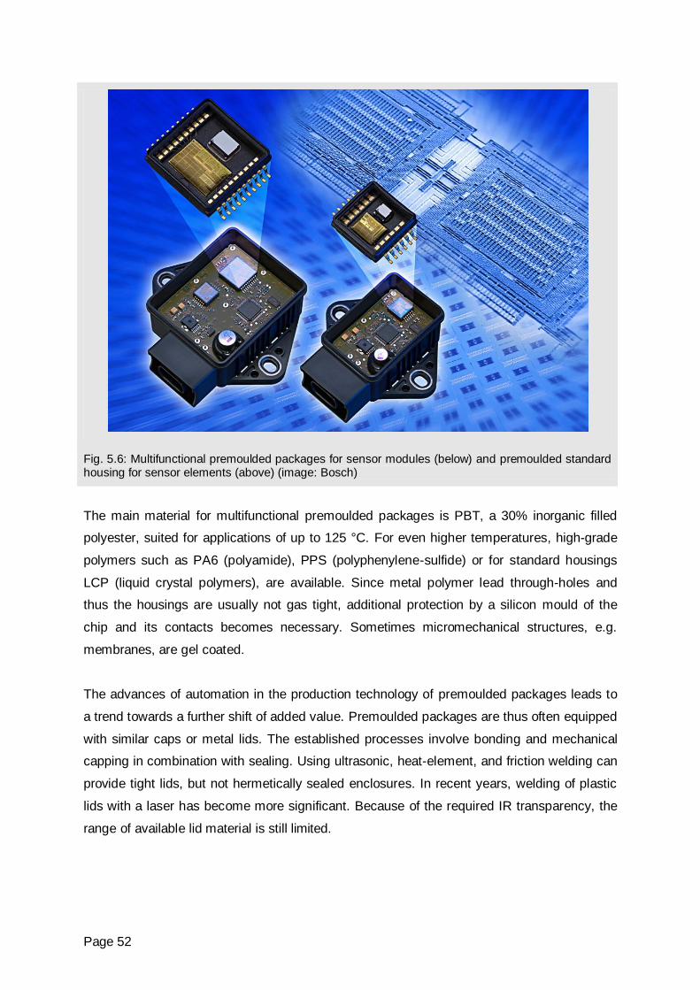
Page 52
Fig. 5.6: Multifunctional premoulded packages for sensor modules (below) and premoulded standard housing for sensor elements (above) (image: Bosch)
The main material for multifunctional premoulded packages is PBT, a 30% inorganic filled
polyester, suited for applications of up to 125 °C. For even higher temperatures, high-grade
polymers such as PA6 (polyamide), PPS (polyphenylene-sulfide) or for standard housings
LCP (liquid crystal polymers), are available. Since metal polymer lead through-holes and
thus the housings are usually not gas tight, additional protection by a silicon mould of the
chip and its contacts becomes necessary. Sometimes micromechanical structures, e.g.
membranes, are gel coated.
The advances of automation in the production technology of premoulded packages leads to
a trend towards a further shift of added value. Premoulded packages are thus often equipped
with similar caps or metal lids. The established processes involve bonding and mechanical
capping in combination with sealing. Using ultrasonic, heat-element, and friction welding can
provide tight lids, but not hermetically sealed enclosures. In recent years, welding of plastic
lids with a laser has become more significant. Because of the required IR transparency, the
range of available lid material is still limited.
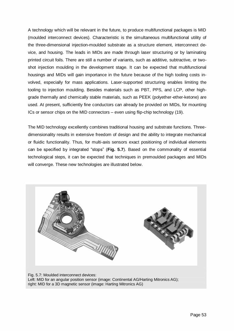
Page 53
A technology which will be relevant in the future, to produce multifunctional packages is MID
(moulded interconnect devices). Characteristic is the simultaneous multifunctional utility of
the three-dimensional injection-moulded substrate as a structure element, interconnect de-
vice, and housing. The leads in MIDs are made through laser structuring or by laminating
printed circuit foils. There are still a number of variants, such as additive, subtractive, or two-
shot injection moulding in the development stage. It can be expected that multifunctional
housings and MIDs will gain importance in the future because of the high tooling costs in-
volved, especially for mass applications. Laser-supported structuring enables limiting the
tooling to injection moulding. Besides materials such as PBT, PPS, and LCP, other high-
grade thermally and chemically stable materials, such as PEEK (polyether-ether-ketone) are
used. At present, sufficiently fine conductors can already be provided on MIDs, for mounting
ICs or sensor chips on the MID connectors – even using flip-chip technology (19).
The MID technology excellently combines traditional housing and substrate functions. Three-
dimensionality results in extensive freedom of design and the ability to integrate mechanical
or fluidic functionality. Thus, for multi-axis sensors exact positioning of individual elements
can be specified by integrated “stops” (Fig. 5.7). Based on the commonality of essential
technological steps, it can be expected that techniques in premoulded packages and MIDs
will converge. These new technologies are illustrated below.
Fig. 5.7: Moulded interconnect devices: Left: MID for an angular position sensor (image: Continental AG/Harting Mitronics AG); right: MID for a 3D magnetic sensor (image: Harting Mitronics AG)
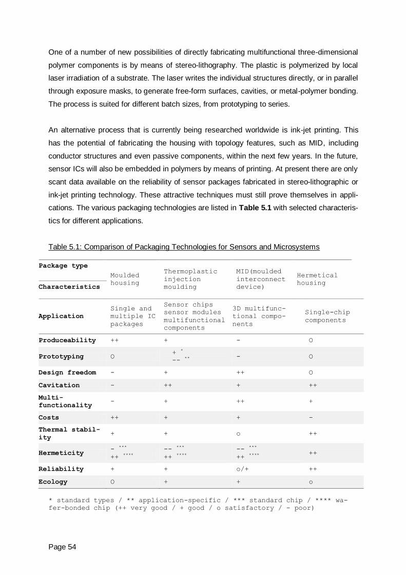
Page 54
One of a number of new possibilities of directly fabricating multifunctional three-dimensional
polymer components is by means of stereo-lithography. The plastic is polymerized by local
laser irradiation of a substrate. The laser writes the individual structures directly, or in parallel
through exposure masks, to generate free-form surfaces, cavities, or metal-polymer bonding.
The process is suited for different batch sizes, from prototyping to series.
An alternative process that is currently being researched worldwide is ink-jet printing. This
has the potential of fabricating the housing with topology features, such as MID, including
conductor structures and even passive components, within the next few years. In the future,
sensor ICs will also be embedded in polymers by means of printing. At present there are only
scant data available on the reliability of sensor packages fabricated in stereo-lithographic or
ink-jet printing technology. These attractive techniques must still prove themselves in appli-
cations. The various packaging technologies are listed in Table 5.1 with selected characteris-
tics for different applications.
Table 5.1: Comparison of Packaging Technologies for Sensors and Microsystems
Package type
Moulded
housing
Thermoplastic
injection
moulding
MID(moulded
interconnect
device)
Hermetical
housing Characteristics
Application
Single and
multiple IC
packages
Sensor chips
sensor modules
multifunctional
components
3D multifunc-
tional compo-
nents
Single-chip
components
Produceability ++ + - O
Prototyping O + *
-- ** - O
Design freedom - + ++ O
Cavitation - ++ + ++
Multi-
functionality - + ++ +
Costs ++ + + -
Thermal stabil-
ity + + o ++
Hermeticity - ***
++ ****
-- ***
++ ****
-- ***
++ **** ++
Reliability + + o/+ ++
Ecology O + + o
* standard types / ** application-specific / *** standard chip / **** wa-
fer-bonded chip (++ very good / + good / o satisfactory / - poor)
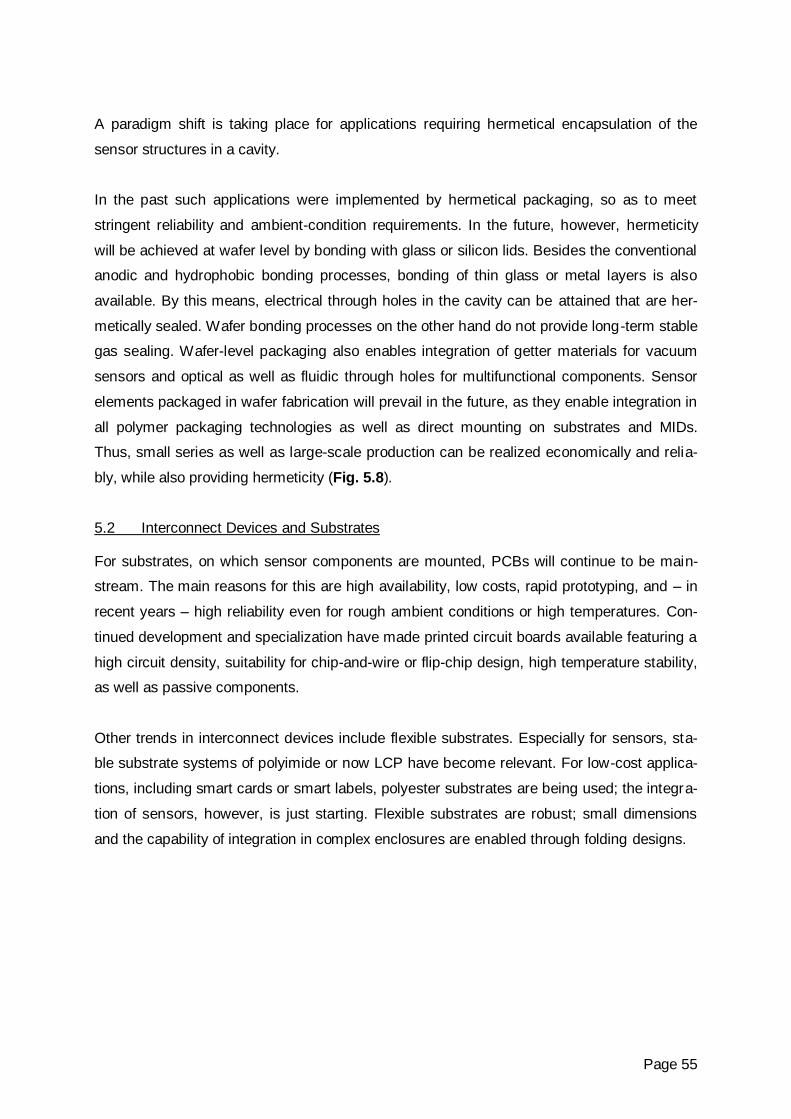
Page 55
A paradigm shift is taking place for applications requiring hermetical encapsulation of the
sensor structures in a cavity.
In the past such applications were implemented by hermetical packaging, so as to meet
stringent reliability and ambient-condition requirements. In the future, however, hermeticity
will be achieved at wafer level by bonding with glass or silicon lids. Besides the conventional
anodic and hydrophobic bonding processes, bonding of thin glass or metal layers is also
available. By this means, electrical through holes in the cavity can be attained that are her-
metically sealed. Wafer bonding processes on the other hand do not provide long-term stable
gas sealing. Wafer-level packaging also enables integration of getter materials for vacuum
sensors and optical as well as fluidic through holes for multifunctional components. Sensor
elements packaged in wafer fabrication will prevail in the future, as they enable integration in
all polymer packaging technologies as well as direct mounting on substrates and MIDs.
Thus, small series as well as large-scale production can be realized economically and relia-
bly, while also providing hermeticity (Fig. 5.8).
5.2 Interconnect Devices and Substrates
For substrates, on which sensor components are mounted, PCBs will continue to be main-
stream. The main reasons for this are high availability, low costs, rapid prototyping, and – in
recent years – high reliability even for rough ambient conditions or high temperatures. Con-
tinued development and specialization have made printed circuit boards available featuring a
high circuit density, suitability for chip-and-wire or flip-chip design, high temperature stability,
as well as passive components.
Other trends in interconnect devices include flexible substrates. Especially for sensors, sta-
ble substrate systems of polyimide or now LCP have become relevant. For low-cost applica-
tions, including smart cards or smart labels, polyester substrates are being used; the integra-
tion of sensors, however, is just starting. Flexible substrates are robust; small dimensions
and the capability of integration in complex enclosures are enabled through folding designs.
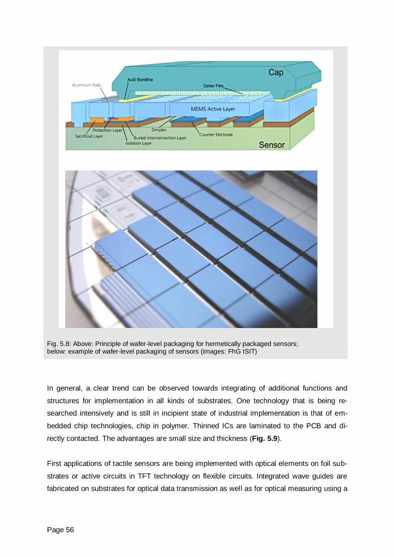
Page 56
Fig. 5.8: Above: Principle of wafer-level packaging for hermetically packaged sensors; below: example of wafer-level packaging of sensors (images: FhG ISIT)
In general, a clear trend can be observed towards integrating of additional functions and
structures for implementation in all kinds of substrates. One technology that is being re-
searched intensively and is still in incipient state of industrial implementation is that of em-
bedded chip technologies, chip in polymer. Thinned ICs are laminated to the PCB and di-
rectly contacted. The advantages are small size and thickness (Fig. 5.9).
First applications of tactile sensors are being implemented with optical elements on foil sub-
strates or active circuits in TFT technology on flexible circuits. Integrated wave guides are
fabricated on substrates for optical data transmission as well as for optical measuring using a
Page 57
broad range of technologies. Thanks especially to improvements in optical coupling, further
applications are on the horizon. Parallel to this development, generation of fluid channels in
polymer substrates has been repeatedly and successfully demonstrated.
Fig. 5.9: Chip-in-polymer functional design 2000+ based on PCB technology (image: Würth Elek-tronik)
Ceramic substrates are essentially dominated by three technologies: The established thick-
film and thin-film hybrids are predestined for stringent electrical requirements, high-
temperature applications, and high reliability. Many applications have been opened in sensor
technology. In the next years, gradual improvements can be expected technologically, espe-
cially in regard to the continued reduction of structure dimensions. For thick-film layers, con-
ductor widths and gaps of approx. 20 µm are expected.
New low-temperature cofired ceramic (LTCC) technology was developed from hybrid tech-
nology. The multilayer ceramics, fired at a relatively low temperature of 850 °C, continue to
have a significant growth potential thanks to characteristics such as simplified multilayer cir-
cuitry, potential three-dimensionality, formability in the green state, and the capability to gen-
erate fluidic elements, such as flow channels and electrodes for the media to be analyzed.
LTTC materials are corrosion proof and temperature stable. The example in Fig. 5.10 is a
16-layer coil to be used as an eddy-current sensor for up to approx. 500 °C. A new concept
for the assembly of media-isolated pressure sensors is based on LTCC for its circuitry ele-
ments. However, limitations result from the limited number of suppliers and because of the
high costs, especially for prototyping. Thus, LTCC will show its benefits in sensor technology
in high-quantity series and in high-end applications.
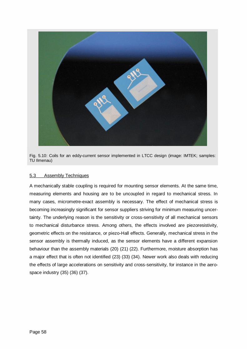
Page 58
Fig. 5.10: Coils for an eddy-current sensor implemented in LTCC design (image: IMTEK; samples: TU Ilmenau)
5.3 Assembly Techniques
A mechanically stable coupling is required for mounting sensor elements. At the same time,
measuring elements and housing are to be uncoupled in regard to mechanical stress. In
many cases, micrometre-exact assembly is necessary. The effect of mechanical stress is
becoming increasingly significant for sensor suppliers striving for minimum measuring uncer-
tainty. The underlying reason is the sensitivity or cross-sensitivity of all mechanical sensors
to mechanical disturbance stress. Among others, the effects involved are piezoresistivity,
geometric effects on the resistance, or piezo-Hall effects. Generally, mechanical stress in the
sensor assembly is thermally induced, as the sensor elements have a different expansion
behaviour than the assembly materials (20) (21) (22). Furthermore, moisture absorption has
a major effect that is often not identified (23) (33) (34). Newer work also deals with reducing
the effects of large accelerations on sensitivity and cross-sensitivity, for instance in the aero-
space industry (35) (36) (37).
Page 59
The measures for reducing stress effects can be divided into three groups:
Thermomechanically compatible assembly techniques
Use of flexible, optimized assembly materials
Increased robustness of the sensor element
For each of these fields, developments and trends in recent years are described below.
1. Thermomechanically Compatible Assembly Technology
The most significant measure taken here is to reduce the thermal expansion coefficients of
substrate, housing, and encapsulation materials. Because silicon is in many cases the domi-
nating sensor material, the expansion coefficients must be compensated. Trends, deriving
from this, are the use of high-grade materials, such as LTCC or other ceramics and the use
of low-stress mould compounds of filled epoxides for encapsulation of large-volume sensors.
In recent years, the compounds available on the market have attained a significant reduction
of the thermal expansion coefficient (approx. 8 ppm/K).
Moreover, an increasing use of advanced layout methods can be observed. Since sensor
designs based on the finite elements method (FEM) are often available in SMBs, complex
assemblies are increasingly being mechanically optimized by the application of the FEM.
Thus, it is now possible to compute stress emergence in sensors during their production as
well as in their application quite exactly (up to < 15%). The effects on the sensor characteris-
tic of Hall and pressure sensors can also be predicted (20) (21) (24).
2. Use of Flexible, Optimized Assembly Materials
The process of sensor assembly by bonding has become widely accepted. For sensor tech-
nology, the relevant materials are epoxides, silicons, and polyimides. Besides adhesion and
permanent joints, the bonding process must also provide electrical contacts and in some
cases thermal coupling to a heat sink. Therefore, bonding materials are often functionalized
with fillers, such as Ag, Al2O3, SiN, or even diamonds. Depending on the application, adhe-
sives with either a high or low glass transition temperature are used. A continued develop-
ment of the materials and processes used in bonding can be observed.
Page 60
3. Increased Robustness of the Sensor Element
This applies to measures taken on the sensor element to reduce the propagation of me-
chanical stress to a minimum. For pressure sensors, for instance, this can be the glass body
that decouples the sensor structure from the substrate. Despite this good effect, develop-
ment trends are more in the direction of reducing the thickness of the glass body and to op-
timize it by applying FEM. Some approaches aim at decoupling the sensor elements through
suitable yielding structures from their substrates. For pressure sensors, for example in form
of silicon bellows or silicon substrates, these have not found wide acceptance. The main ob-
stacle besides the micromechanical complexity was the significant loss of active silicon sur-
face area on the wafer. This is usually not tolerated. Whenever suitable suspension struc-
tures can be integrated in micromechanical sensor assemblies, these are used successfully.
This applies especially to angular rate sensors (gyroscopes), for which a complex, multi-
axial, statically and dynamically balanced suspension is imperative.
5.4 Bonding Techniques
The dominating bonding techniques relevant for sensors in the next few years are already
largely available.
Ball-wedge wire bonding with pure gold wires is already at a high level of process stability
and reliability. Thus for the bonds, minimal error rates of a few ppm are attained. Thanks to
new technical devices, a trend towards wedge-wedge bonding with aluminium wire (AlSi1)
was observed for non-IC applications, that will probably continue into the future. The signifi-
cant advantages, such as a high degree of flexibility, low costs even for small batches, and
simple prototyping, will allow both wire bonding techniques to dominate in sensor technology,
especially for low quantities. Moreover, wire bonds keep their long-term stability at operating
temperatures of up to 200 °C – or even higher for good metallurgical adaptation.
Both techniques now enable wire diameters of less than 20 µm. Deciding which of the two
bonding techniques are to be implemented depends on such factors as topology, metallurgy,
and bonding speed. For integrated sensor-actuator systems requiring currents in the ampere
range, wire bonding with aluminium wire or Al-strips will find increasing acceptance. In regard
to safety applications, such as in medical technology, good verifiability of wire bonds with
destructive and non-destructive process is a major advantage. For wire bonding in general
detail improvements at a high level can be expected and it will therefore maintain its domi-
nant position in many applications in sensor technology.
Page 61
The flip-chip technique is based on the principles of adhesion, thermo-compression bonding,
or soldering. Flip-chip assembly is implemented in both, SMD processes and special FC
bonding devices. The rise in these technologies is a consequence of the technical require-
ments that cannot be met otherwise, e.g. for RF applications. Due to the significantly lower
inductivities compared to wire bonds, fast signals in flip-chip contacts will be considerably
less delayed. For optical components, such as CCD chips, the high contact parallelism offers
advantages for fabrication, economy, and dimensions. Thus already more than ten years
ago, in singular, non-cost-critical applications (CCD IR sensors) bump pitches of less than 25
µm were industrially produced for hundreds of connections. It is to be expected that such
characteristics will become available in series for a wide range of applications. In general, a
continued improvement in the supplier infrastructures of flip-chip technology can be assumed
for the next years. In this context, suppliers of bumped sensor ICs, service providers for wa-
fer bumping, device manufacturers, and material suppliers (e.g. of adhesives) may be men-
tioned. Thus, for system developers in sensor technology, it will be easier in future to realize
a variant in flip-chip technique.
At the assembly level, soldering with lead-free solder is being qualified at present. The re-
sults up to now show that on the average reliability data can be expected that is comparable
to SnPb solders and that these soldering materials will have a better temperature stability of
about 10 to 20 K than SnPb alloys. However, the reliability must be proven for the specific
application. Overall, it can be expected that lead containing solder will be widely replaced –
also in sensor technology – even if this is not required by law.
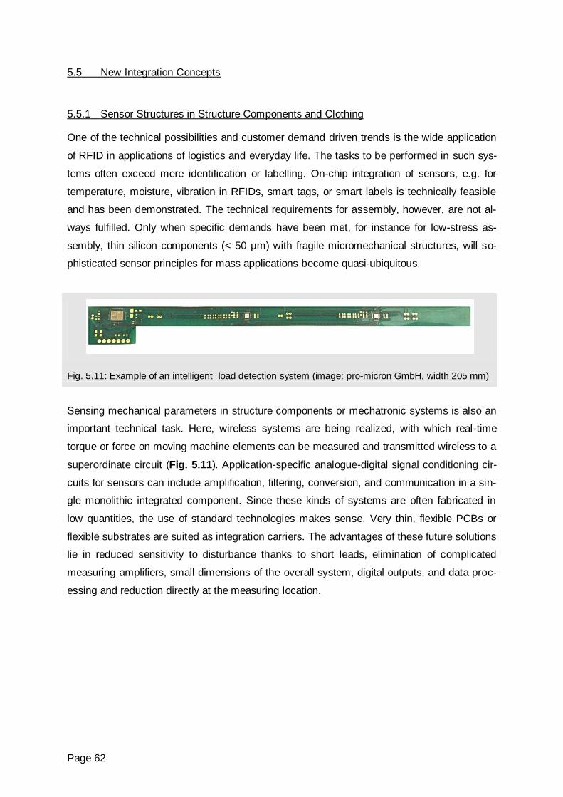
Page 62
5.5 New Integration Concepts
5.5.1 Sensor Structures in Structure Components and Clothing
One of the technical possibilities and customer demand driven trends is the wide application
of RFID in applications of logistics and everyday life. The tasks to be performed in such sys-
tems often exceed mere identification or labelling. On-chip integration of sensors, e.g. for
temperature, moisture, vibration in RFIDs, smart tags, or smart labels is technically feasible
and has been demonstrated. The technical requirements for assembly, however, are not al-
ways fulfilled. Only when specific demands have been met, for instance for low-stress as-
sembly, thin silicon components (< 50 µm) with fragile micromechanical structures, will so-
phisticated sensor principles for mass applications become quasi-ubiquitous.
Fig. 5.11: Example of an intelligent load detection system (image: pro-micron GmbH, width 205 mm)
Sensing mechanical parameters in structure components or mechatronic systems is also an
important technical task. Here, wireless systems are being realized, with which real-time
torque or force on moving machine elements can be measured and transmitted wireless to a
superordinate circuit (Fig. 5.11). Application-specific analogue-digital signal conditioning cir-
cuits for sensors can include amplification, filtering, conversion, and communication in a sin-
gle monolithic integrated component. Since these kinds of systems are often fabricated in
low quantities, the use of standard technologies makes sense. Very thin, flexible PCBs or
flexible substrates are suited as integration carriers. The advantages of these future solutions
lie in reduced sensitivity to disturbance thanks to short leads, elimination of complicated
measuring amplifiers, small dimensions of the overall system, digital outputs, and data proc-
essing and reduction directly at the measuring location.
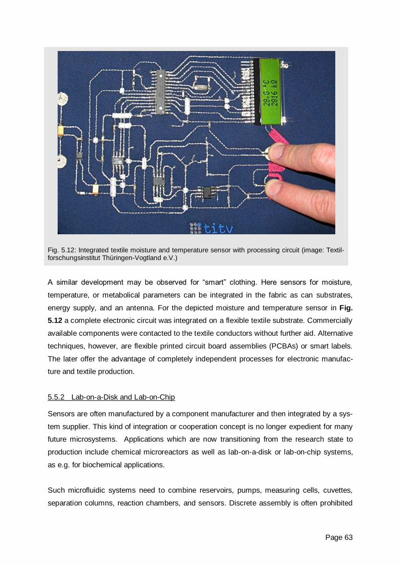
Page 63
Fig. 5.12: Integrated textile moisture and temperature sensor with processing circuit (image: Textil-forschungsinstitut Thüringen-Vogtland e.V.)
A similar development may be observed for “smart” clothing. Here sensors for moisture,
temperature, or metabolical parameters can be integrated in the fabric as can substrates,
energy supply, and an antenna. For the depicted moisture and temperature sensor in Fig.
5.12 a complete electronic circuit was integrated on a flexible textile substrate. Commercially
available components were contacted to the textile conductors without further aid. Alternative
techniques, however, are flexible printed circuit board assemblies (PCBAs) or smart labels.
The later offer the advantage of completely independent processes for electronic manufac-
ture and textile production.
5.5.2 Lab-on-a-Disk and Lab-on-Chip
Sensors are often manufactured by a component manufacturer and then integrated by a sys-
tem supplier. This kind of integration or cooperation concept is no longer expedient for many
future microsystems. Applications which are now transitioning from the research state to
production include chemical microreactors as well as lab-on-a-disk or lab-on-chip systems,
as e.g. for biochemical applications.
Such microfluidic systems need to combine reservoirs, pumps, measuring cells, cuvettes,
separation columns, reaction chambers, and sensors. Discrete assembly is often prohibited
Page 64
due to the dimensions, dead volumes, dead times, and costs. Such fluidic systems are as-
sembled monolithically or in hybrid assembly using as few individual components as possi-
ble. Typical sensors to be integrated detect temperature, volume and mass flow, pressure,
colour, or chemical parameters. Moreover, they have integrated cavities for optical meas-
urement of media characteristics with external analysis systems. Therefore, the developer
will design and fabricate simple sensors in the future as elementary constituent system parts.
In other cases it will become necessary to integrate e.g. the sensor IC as a bare chip. In such
cases, the application-specific sensor knowhow resides at the system house and not at the
sensor manufacturer.
Many of the sensor suppliers represented in the AMA generate added value through their
application-specific knowledge to meet industry-specific specifications and standards. For
monolithically integrated chemical or fluidic systems, a strategy for added value creation
might be to target system leadership for such microsystems and thus develop from a sensor
supplier to a microsystem supplier.
5.5.3 Medical Technology
In medical technology, a considerable R&D effort is being committed to the development of
new sensor, actuator, or stimulation systems for in-vivo applications. These are made to be
implanted permanently or temporarily in patients to replace essential bodily functions. With
the aid of neuroprosthetics, interfaces to nerves are being created; other applications require
access to the skin or body fluids. Besides the stimulation of nerves and detection of nerve
signals, other in-vivo applications deal with sensing metabolical parameters or dosage of
medications.
For in-vivo systems in the demonstrator state or in animal experiments, a standard packag-
ing process has been developed, driven by biocompatibility requirements, and targeted at
mass applications. In many cases, flexible substrates are used, on which integrated circuits
or sensors are usually mounted as bare chips. The flexible substrate is used as a carrier for
electrodes and for sheathing nerve cells.
To counteract the low resistance of silicon materials to media diffusion, additional thin protec-
tive layers are applied for passivation. Here, CVD or PVD layers of parylene, glass, oxides,
nitrides, or SiC are being tested.
Page 65
6 Development Trends –
Testing Processes for MEMS Components
Abstract
Many new sensor types are based on MEMS technology and suppliers are expending great
efforts totest conductivity, quality, and reliability. Moreover, comprehensive tests are per-
formed for checking production steps as well as for field monitoring and self-testing of MEMS
components. This chapter describes the various tests that are carried out on MEMS-based
sensors. It also illustrates how these methods can be applied as part of a comprehensive
quality strategy.
For testing MEMS components there is a strong tendency towards characterizing sensor
functions and cross-sensitivities as early and as comprehensively as possible. On the wafer
level this is achieved by wafer-level tests with physical stimulation:
Via a probe
Via a chuck
For both surface and bulk micromechanics, there is a trend to integrate built-in self-tests
(BISTs). Internal structures are used to stimulate the transducer structure. There is also a
trend towards sensors with self-calibration capabilities.
6.1 Fault Types
For micro-electronic systems two basic types of fault can be distinguished. The first group
comprises faults that lead to complete malfunction. The second group consists of parametric
faults, systematic and random faults that change the characteristic or transient behaviour
(Table 6.2).
For constituent mechanical parts of MEMS, a total failure can be due to broken or non-
separated structures (Table 6.1). If this has impacted functional parameters, often either
mass, rigidity, or an attenuation coefficient are out of the permissible range. In such cases,
static and dynamic behaviour is noticeably impaired. Thus, functional behaviour may be an
indirect indication of physical defects of the micromechanical elements. The effectiveness of
the various testing concepts can be determined by means of physical failure models and
simulation using the finite elements method. An example of this is the effect of vacuum qual-
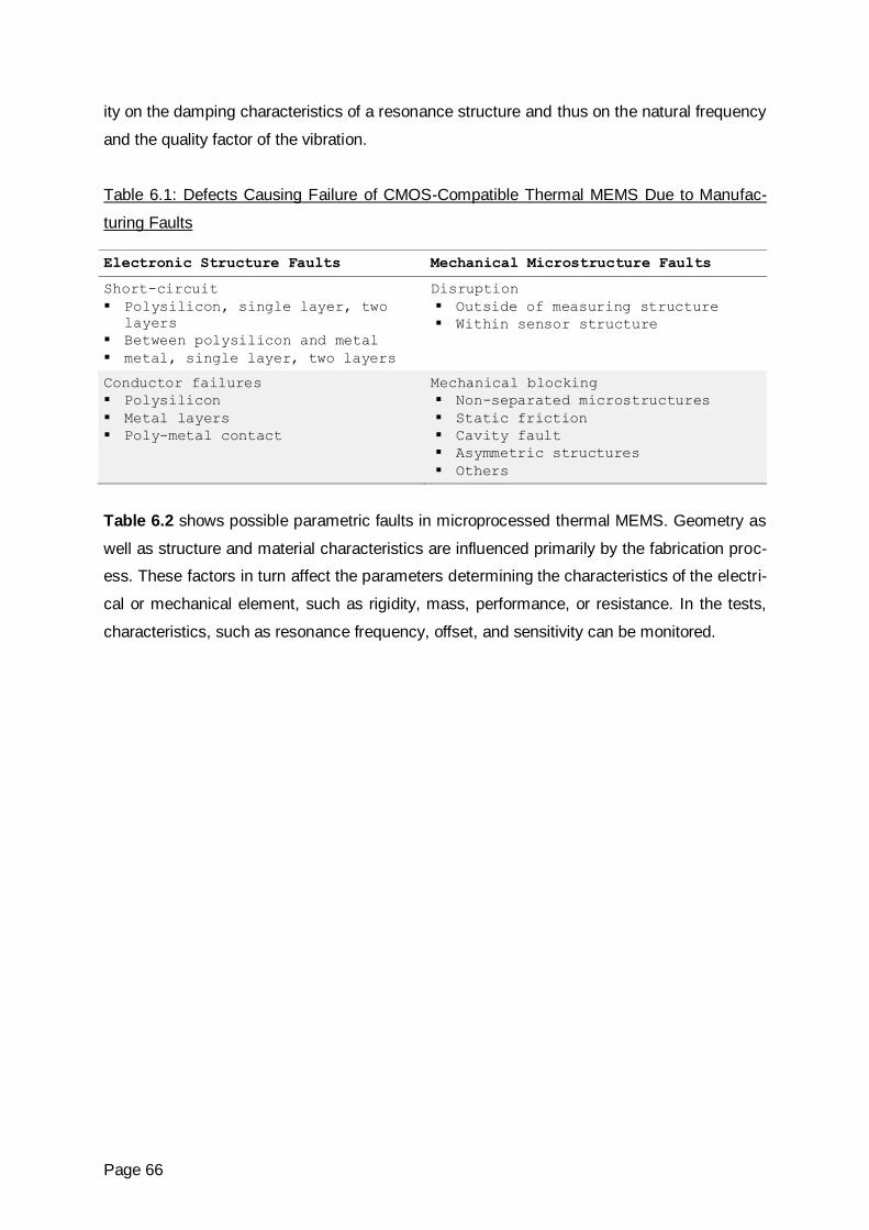
Page 66
ity on the damping characteristics of a resonance structure and thus on the natural frequency
and the quality factor of the vibration.
Table 6.1: Defects Causing Failure of CMOS-Compatible Thermal MEMS Due to Manufac-
turing Faults
Electronic Structure Faults Mechanical Microstructure Faults
Short-circuit
Polysilicon, single layer, two
layers
Between polysilicon and metal
metal, single layer, two layers
Disruption
Outside of measuring structure
Within sensor structure
Conductor failures
Polysilicon
Metal layers
Poly-metal contact
Mechanical blocking
Non-separated microstructures
Static friction
Cavity fault
Asymmetric structures
Others
Table 6.2 shows possible parametric faults in microprocessed thermal MEMS. Geometry as
well as structure and material characteristics are influenced primarily by the fabrication proc-
ess. These factors in turn affect the parameters determining the characteristics of the electri-
cal or mechanical element, such as rigidity, mass, performance, or resistance. In the tests,
characteristics, such as resonance frequency, offset, and sensitivity can be monitored.
Page 67
Table 6.2: Classification of Parametric Faults for Microprocessed Thermal MEMS, According
to (18)
Mechanical Electrical
Structure characteristics
Edge defects, width, length,
thickness
Cavity faults
Friction and adhesion
Missing structures
Partial suspension or detach-
ment of structures
Vacuum quality or pressure
Structure characteristics of conduc-
tors
Width
Length
Thickness
Doping profile
...
Thermomechanical material charac-
teristics
Density
Elasticity modulus
Thermal expansion coefficient
of metal
Thermal conductivity and capac-
ity
Radiation emission coefficient
Convection coefficient
Friction coefficient
Thermo-electrical material characteris-
tics
Specific resistance of polysilicon
and metal
Contact resistance
Temperature coefficient of polysili-
con and metal
Piezoresistive coefficient of sili-
con
Seebeck coefficient of polysilicon
and metal
Dielectric constant and loss factor
Variation of mechanical coeffi-
cients
Rigidity, resilience
Mass
Attenuation factor / viscosity
...
Electrical interference components
Parasitic resistances
Parasitic capacities
Parasitic inductivities
...
System behaviour
Natural frequency
Quality factor
Nonlinearity
System behaviour
Offset shifts
Sensitivity changes
Changes in characteristic impedance
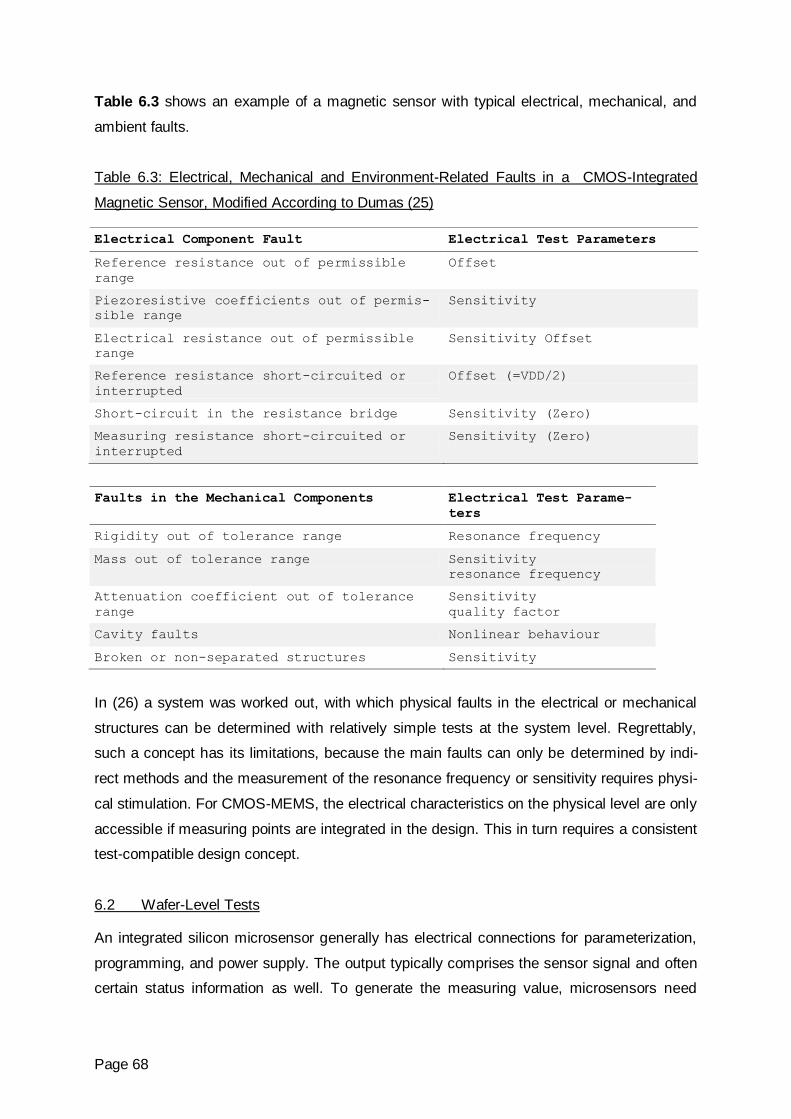
Page 68
Table 6.3 shows an example of a magnetic sensor with typical electrical, mechanical, and
ambient faults.
Table 6.3: Electrical, Mechanical and Environment-Related Faults in a CMOS-Integrated
Magnetic Sensor, Modified According to Dumas (25)
Electrical Component Fault Electrical Test Parameters
Reference resistance out of permissible
range
Offset
Piezoresistive coefficients out of permis-
sible range
Sensitivity
Electrical resistance out of permissible
range
Sensitivity Offset
Reference resistance short-circuited or
interrupted
Offset (=VDD/2)
Short-circuit in the resistance bridge Sensitivity (Zero)
Measuring resistance short-circuited or
interrupted
Sensitivity (Zero)
Faults in the Mechanical Components Electrical Test Parame-
ters
Rigidity out of tolerance range Resonance frequency
Mass out of tolerance range Sensitivity
resonance frequency
Attenuation coefficient out of tolerance
range
Sensitivity
quality factor
Cavity faults Nonlinear behaviour
Broken or non-separated structures Sensitivity
In (26) a system was worked out, with which physical faults in the electrical or mechanical
structures can be determined with relatively simple tests at the system level. Regrettably,
such a concept has its limitations, because the main faults can only be determined by indi-
rect methods and the measurement of the resonance frequency or sensitivity requires physi-
cal stimulation. For CMOS-MEMS, the electrical characteristics on the physical level are only
accessible if measuring points are integrated in the design. This in turn requires a consistent
test-compatible design concept.
6.2 Wafer-Level Tests
An integrated silicon microsensor generally has electrical connections for parameterization,
programming, and power supply. The output typically comprises the sensor signal and often
certain status information as well. To generate the measuring value, microsensors need
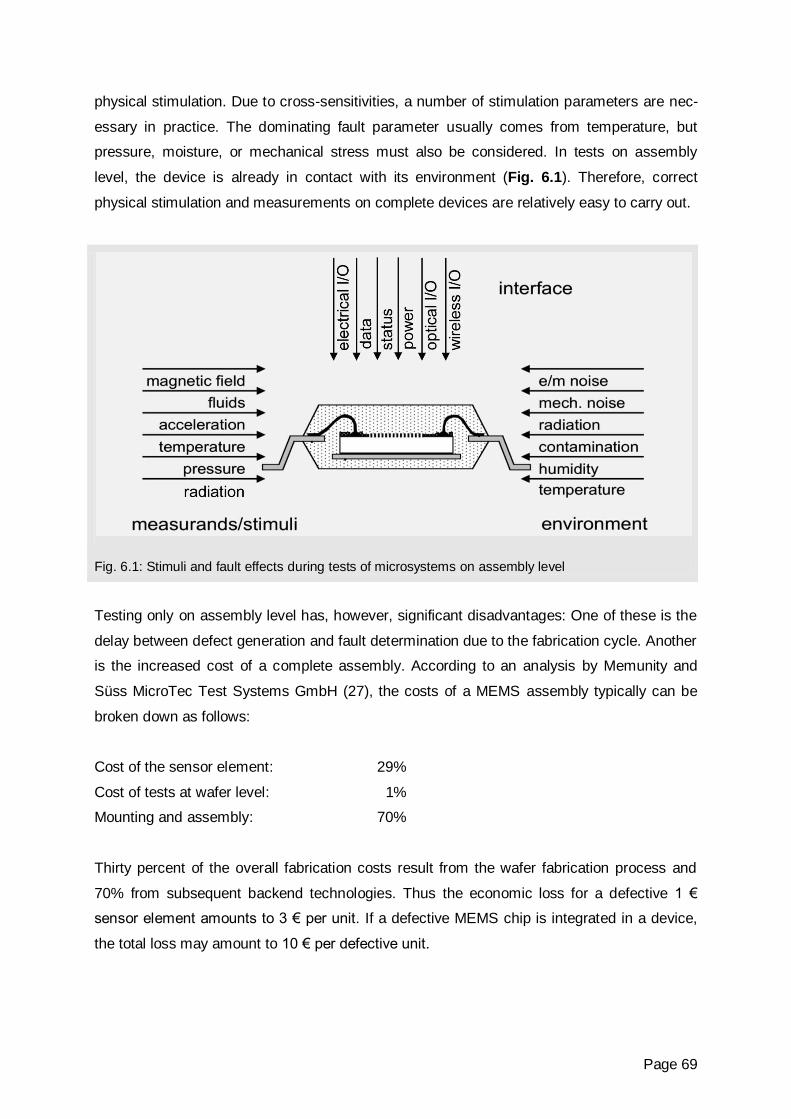
Page 69
physical stimulation. Due to cross-sensitivities, a number of stimulation parameters are nec-
essary in practice. The dominating fault parameter usually comes from temperature, but
pressure, moisture, or mechanical stress must also be considered. In tests on assembly
level, the device is already in contact with its environment (Fig. 6.1). Therefore, correct
physical stimulation and measurements on complete devices are relatively easy to carry out.
Fig. 6.1: Stimuli and fault effects during tests of microsystems on assembly level
Testing only on assembly level has, however, significant disadvantages: One of these is the
delay between defect generation and fault determination due to the fabrication cycle. Another
is the increased cost of a complete assembly. According to an analysis by Memunity and
Süss MicroTec Test Systems GmbH (27), the costs of a MEMS assembly typically can be
broken down as follows:
Cost of the sensor element: 29%
Cost of tests at wafer level: 1%
Mounting and assembly: 70%
Thirty percent of the overall fabrication costs result from the wafer fabrication process and
70% from subsequent backend technologies. Thus the economic loss for a defective 1 €
sensor element amounts to 3 € per unit. If a defective MEMS chip is integrated in a device,
the total loss may amount to 10 € per defective unit.

Page 70
Another important aspect to consider is the time required to feed the failure information back
into the production process. Fault analysis of an encapsulated unit can be tedious. The sili-
con chip requires artefact-free fabrication. Moreover, mounting and assembly do not take
place in a clean room, but in another factory site. It can be a matter of weeks or even months
before the fault data reaches the wafer factory. The data is thus not up to date and will influ-
ence wafer quality very late.
Early in-production testing of microsystems of bare chips must therefore be a major consid-
eration in modern test strategies. For (non-MEMS) ICs it was shown that wafer-level tests
are considerably more efficient than tests on individual unhoused sensor elements. Func-
tional testing of individual sensor elements requires costly adapters and would be considera-
bly more expensive than the 10% share of costs for testing at wafer-level. Modern testing
strategy makes use of both concepts for MEMS testing at the wafer level and at the compo-
nent level to optimize throughput, accuracy, reliability, and the overall acquisition of data.
Therefore the costs for testing and calibration are relatively high compared to the production
costs.
The following sections evaluate the available technical solutions for testing MEMS at the wa-
fer level.
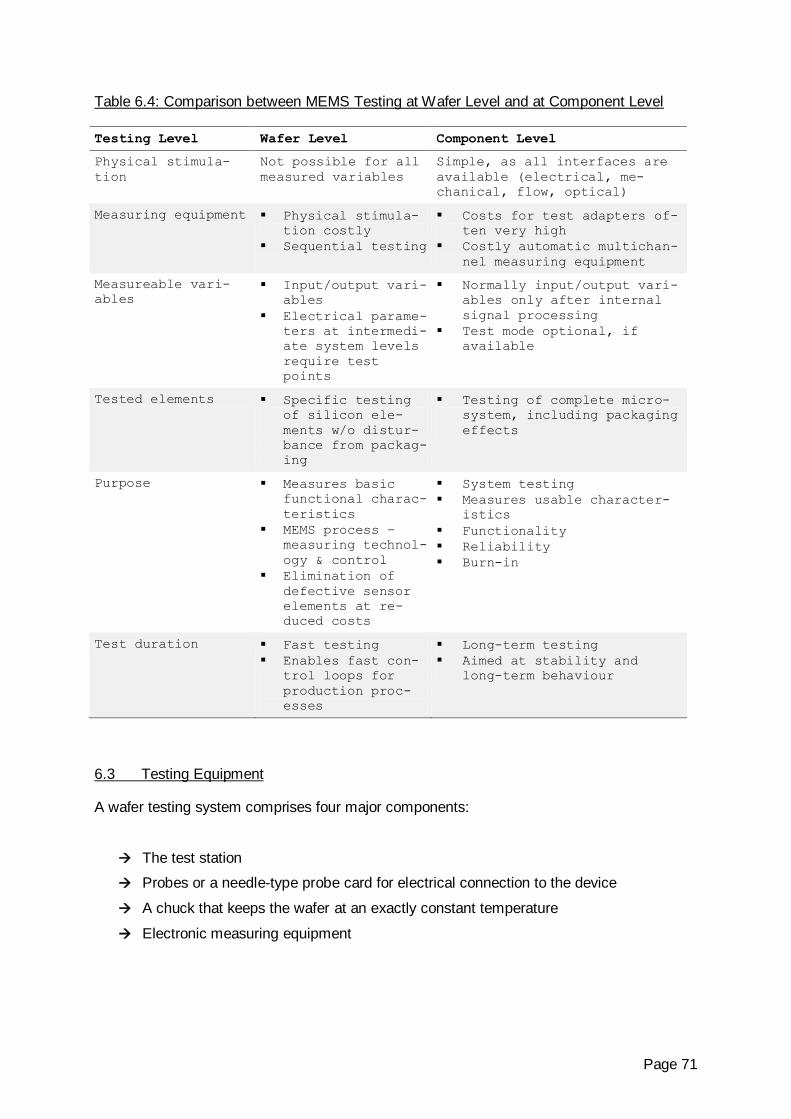
Page 71
Table 6.4: Comparison between MEMS Testing at Wafer Level and at Component Level
Testing Level Wafer Level Component Level
Physical stimula-
tion
Not possible for all
measured variables
Simple, as all interfaces are
available (electrical, me-
chanical, flow, optical)
Measuring equipment Physical stimula-
tion costly
Sequential testing
Costs for test adapters of-
ten very high
Costly automatic multichan-
nel measuring equipment
Measureable vari-
ables
Input/output vari-
ables
Electrical parame-
ters at intermedi-
ate system levels
require test
points
Normally input/output vari-
ables only after internal
signal processing
Test mode optional, if
available
Tested elements Specific testing
of silicon ele-
ments w/o distur-
bance from packag-
ing
Testing of complete micro-
system, including packaging
effects
Purpose Measures basic
functional charac-
teristics
MEMS process –
measuring technol-
ogy & control
Elimination of
defective sensor
elements at re-
duced costs
System testing
Measures usable character-
istics
Functionality
Reliability
Burn-in
Test duration Fast testing
Enables fast con-
trol loops for
production proc-
esses
Long-term testing
Aimed at stability and
long-term behaviour
6.3 Testing Equipment
A wafer testing system comprises four major components:
The test station
Probes or a needle-type probe card for electrical connection to the device
A chuck that keeps the wafer at an exactly constant temperature
Electronic measuring equipment
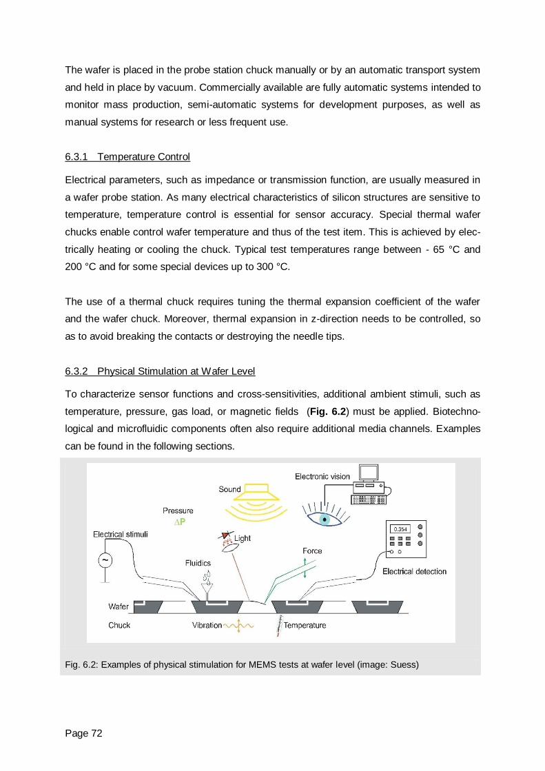
Page 72
The wafer is placed in the probe station chuck manually or by an automatic transport system
and held in place by vacuum. Commercially available are fully automatic systems intended to
monitor mass production, semi-automatic systems for development purposes, as well as
manual systems for research or less frequent use.
6.3.1 Temperature Control
Electrical parameters, such as impedance or transmission function, are usually measured in
a wafer probe station. As many electrical characteristics of silicon structures are sensitive to
temperature, temperature control is essential for sensor accuracy. Special thermal wafer
chucks enable control wafer temperature and thus of the test item. This is achieved by elec-
trically heating or cooling the chuck. Typical test temperatures range between - 65 °C and
200 °C and for some special devices up to 300 °C.
The use of a thermal chuck requires tuning the thermal expansion coefficient of the wafer
and the wafer chuck. Moreover, thermal expansion in z-direction needs to be controlled, so
as to avoid breaking the contacts or destroying the needle tips.
6.3.2 Physical Stimulation at Wafer Level
To characterize sensor functions and cross-sensitivities, additional ambient stimuli, such as
temperature, pressure, gas load, or magnetic fields (Fig. 6.2) must be applied. Biotechno-
logical and microfluidic components often also require additional media channels. Examples
can be found in the following sections.
Fig. 6.2: Examples of physical stimulation for MEMS tests at wafer level (image: Suess)
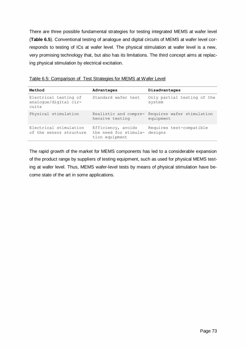
Page 73
There are three possible fundamental strategies for testing integrated MEMS at wafer level
(Table 6.5). Conventional testing of analogue and digital circuits of MEMS at wafer level cor-
responds to testing of ICs at wafer level. The physical stimulation at wafer level is a new,
very promising technology that, but also has its limitations. The third concept aims at replac-
ing physical stimulation by electrical excitation.
Table 6.5: Comparison of Test Strategies for MEMS at Wafer Level
Method Advantages Disadvantages
Electrical testing of
analogue/digital cir-
cuits
Standard wafer test Only partial testing of the
system
Physical stimulation Realistic and compre-
hensive testing
Requires wafer stimulation
equipment
Electrical stimulation
of the sensor structure
Efficiency, avoids
the need for stimula-
tion equipment
Requires test-compatible
designs
The rapid growth of the market for MEMS components has led to a considerable expansion
of the product range by suppliers of testing equipment, such as used for physical MEMS test-
ing at wafer level. Thus, MEMS wafer-level tests by means of physical stimulation have be-
come state of the art in some applications.
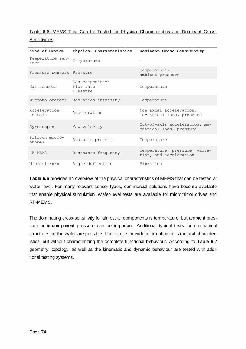
Page 74
Table 6.6: MEMS That Can be Tested for Physical Characteristics and Dominant Cross-
Sensitivities
Kind of Device Physical Characteristics Dominant Cross-Sensitivity
Temperature sen-
sors Temperature -
Pressure sensors Pressure Temperature,
ambient pressure
Gas sensors
Gas composition
Flow rate
Pressure
Temperature
Microbolometers Radiation intensity Temperature
Acceleration
sensors Acceleration
Non-axial acceleration,
mechanical load, pressure
Gyroscopes Yaw velocity Out-of-axis acceleration, me-
chanical load, pressure
Silicon micro-
phones Acoustic pressure Temperature
HF-MEMS Resonance frequency Temperature, pressure, vibra-
tion, and acceleration
Micromirrors Angle deflection Vibration
Table 6.6 provides an overview of the physical characteristics of MEMS that can be tested at
wafer level. For many relevant sensor types, commercial solutions have become available
that enable physical stimulation. Wafer-level tests are available for micromirror drives and
RF-MEMS.
The dominating cross-sensitivity for almost all components is temperature, but ambient pres-
sure or in-component pressure can be important. Additional typical tests for mechanical
structures on the wafer are possible. These tests provide information on structural character-
istics, but without characterizing the complete functional behaviour. According to Table 6.7
geometry, topology, as well as the kinematic and dynamic behaviour are tested with addi-
tional testing systems.
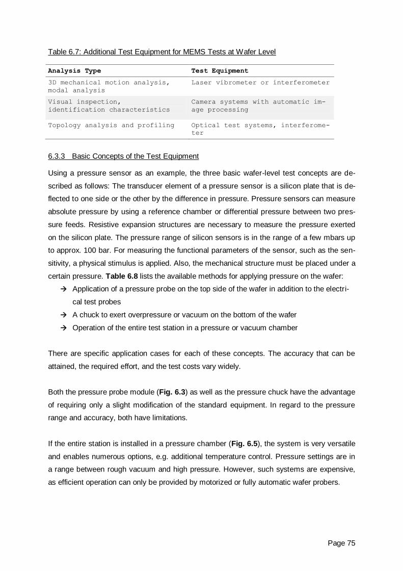
Page 75
Table 6.7: Additional Test Equipment for MEMS Tests at Wafer Level
Analysis Type Test Equipment
3D mechanical motion analysis,
modal analysis
Laser vibrometer or interferometer
Visual inspection,
identification characteristics
Camera systems with automatic im-
age processing
Topology analysis and profiling Optical test systems, interferome-
ter
6.3.3 Basic Concepts of the Test Equipment
Using a pressure sensor as an example, the three basic wafer-level test concepts are de-
scribed as follows: The transducer element of a pressure sensor is a silicon plate that is de-
flected to one side or the other by the difference in pressure. Pressure sensors can measure
absolute pressure by using a reference chamber or differential pressure between two pres-
sure feeds. Resistive expansion structures are necessary to measure the pressure exerted
on the silicon plate. The pressure range of silicon sensors is in the range of a few mbars up
to approx. 100 bar. For measuring the functional parameters of the sensor, such as the sen-
sitivity, a physical stimulus is applied. Also, the mechanical structure must be placed under a
certain pressure. Table 6.8 lists the available methods for applying pressure on the wafer:
Application of a pressure probe on the top side of the wafer in addition to the electri-
cal test probes
A chuck to exert overpressure or vacuum on the bottom of the wafer
Operation of the entire test station in a pressure or vacuum chamber
There are specific application cases for each of these concepts. The accuracy that can be
attained, the required effort, and the test costs vary widely.
Both the pressure probe module (Fig. 6.3) as well as the pressure chuck have the advantage
of requiring only a slight modification of the standard equipment. In regard to the pressure
range and accuracy, both have limitations.
If the entire station is installed in a pressure chamber (Fig. 6.5), the system is very versatile
and enables numerous options, e.g. additional temperature control. Pressure settings are in
a range between rough vacuum and high pressure. However, such systems are expensive,
as efficient operation can only be provided by motorized or fully automatic wafer probers.
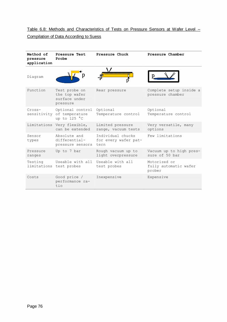
Page 76
Table 6.8: Methods and Characteristics of Tests on Pressure Sensors at Wafer Level –
Compilation of Data According to Suess
Method of
pressure
application
Pressure Test
Probe
Pressure Chuck Pressure Chamber
Diagram
Function Test probe on
the top wafer
surface under
pressure
Rear pressure Complete setup inside a
pressure chamber
Cross-
sensitivity
Optional control
of temperature
up to 125 °C
Optional
Temperature control
Optional
Temperature control
Limitations Very flexible,
can be extended
Limited pressure
range, vacuum tests
Very versatile, many
options
Sensor
types
Absolute and
differential-
pressure sensors
Individual chucks
for every wafer pat-
tern
Few limitations
Pressure
ranges
Up to 7 bar Rough vacuum up to
light overpressure
Vacuum up to high pres-
sure of 50 bar
Testing
limitations
Useable with all
test probes
Useable with all
test probes
Motorized or
fully automatic wafer
prober
Costs Good price /
performance ra-
tio
Inexpensive Expensive
ppp
-pp
-p-p-p pp
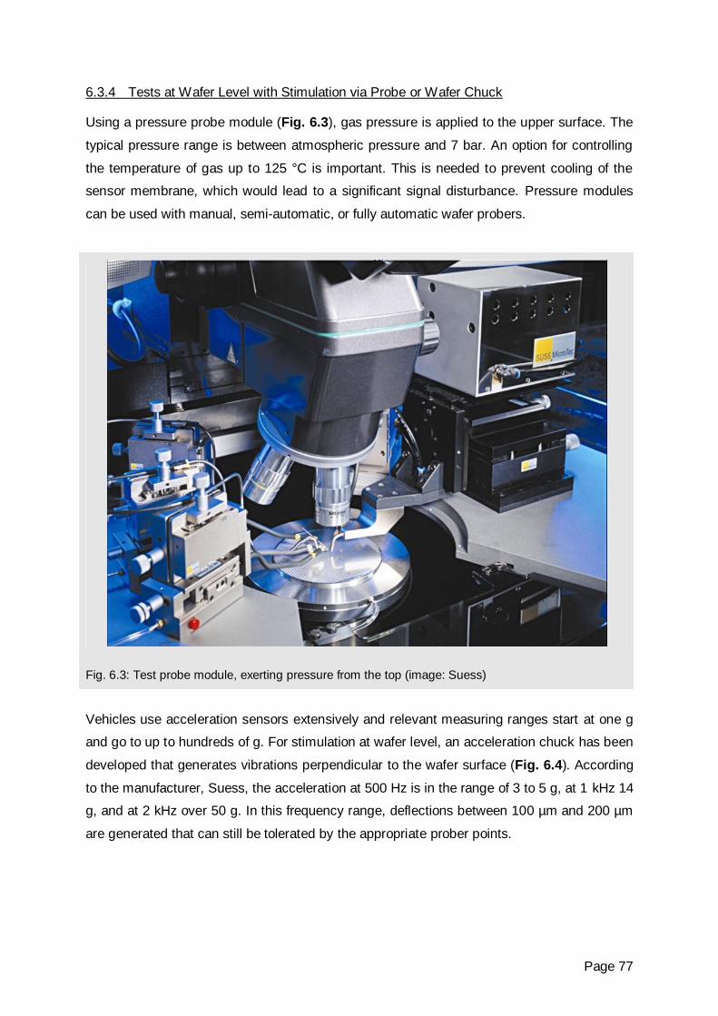
Page 77
6.3.4 Tests at Wafer Level with Stimulation via Probe or Wafer Chuck
Using a pressure probe module (Fig. 6.3), gas pressure is applied to the upper surface. The
typical pressure range is between atmospheric pressure and 7 bar. An option for controlling
the temperature of gas up to 125 °C is important. This is needed to prevent cooling of the
sensor membrane, which would lead to a significant signal disturbance. Pressure modules
can be used with manual, semi-automatic, or fully automatic wafer probers.
Fig. 6.3: Test probe module, exerting pressure from the top (image: Suess)
Vehicles use acceleration sensors extensively and relevant measuring ranges start at one g
and go to up to hundreds of g. For stimulation at wafer level, an acceleration chuck has been
developed that generates vibrations perpendicular to the wafer surface (Fig. 6.4). According
to the manufacturer, Suess, the acceleration at 500 Hz is in the range of 3 to 5 g, at 1 kHz 14
g, and at 2 kHz over 50 g. In this frequency range, deflections between 100 µm and 200 µm
are generated that can still be tolerated by the appropriate prober points.
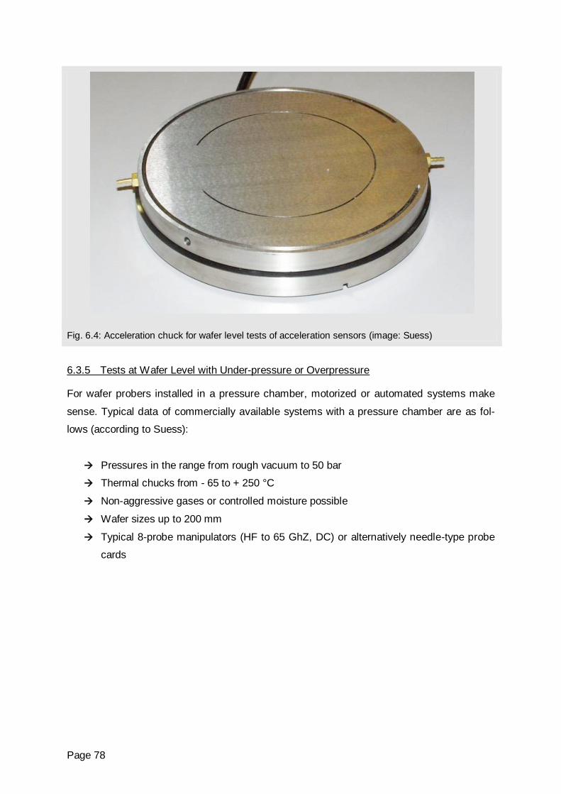
Page 78
Fig. 6.4: Acceleration chuck for wafer level tests of acceleration sensors (image: Suess)
6.3.5 Tests at Wafer Level with Under-pressure or Overpressure
For wafer probers installed in a pressure chamber, motorized or automated systems make
sense. Typical data of commercially available systems with a pressure chamber are as fol-
lows (according to Suess):
Pressures in the range from rough vacuum to 50 bar
Thermal chucks from - 65 to + 250 °C
Non-aggressive gases or controlled moisture possible
Wafer sizes up to 200 mm
Typical 8-probe manipulators (HF to 65 GhZ, DC) or alternatively needle-type probe
cards
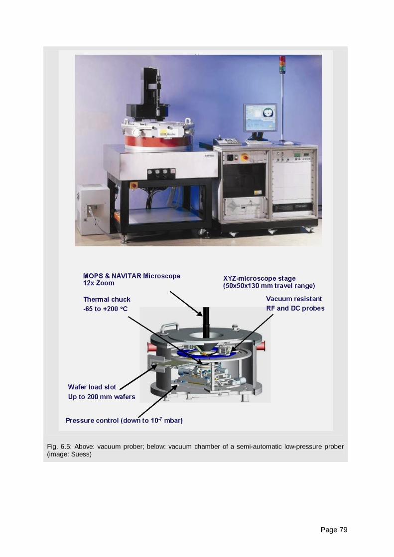
Page 79
Fig. 6.5: Above: vacuum prober; below: vacuum chamber of a semi-automatic low-pressure prober (image: Suess)
Page 80
Many MEMS types need to be tested in vacuum or in specially controlled atmospheres, such
as RF-MEMS, micromirrors, resonators, and mass sensors. Low pressures are also needed
for testing microbolometers for infrared imaging, pressure sensors, chemical sensors, and
MEMS for aerospace applications. A special vacuum test station is required if tests are to be
performed at wafer level. Such a station includes a complete prober with manipulators in a
vacuum chamber (Fig. 6.5), allowing all degrees of freedom. Depending on the vacuum
chamber, control of pressure from high vacuum (10-7 mbar) to atmospheric pressure are
possible.
6.3.6 Application of Tests at Wafer Level
6.3.6.1 Gas Sensors
Based on legal requirements as well as safety and convenience features demanded by us-
ers, MEMS gas sensors are becoming increasingly important. In the application areas of
automotive engineering, industry, or households, there is an increasing demand to monitor
exhaust and toxic gases such as COX or NOX. The use of vacuum or low-pressure chambers
in conjunction with flow controls enable contactless and accurate dosing of gases down to
the ppm range.
An economical alternative is to apply the gases to the sensors at the wafer level using an
electrical test probe and a gas nozzle (see Fig. 6.3). Since this only allows measurements
with limited accuracy, it should therefore be limited to application with non-toxic media.
6.3.6.2 RF-MEMS
Testing in a vacuum is absolutely necessary for MEMS that are to be operated at high fre-
quencies. For mechanically switching elements, vacuum avoids adhesion effects, moisturiza-
tion of mechanical structures, as well as the effects of air viscosity and acoustic interferences
in the cavity. Recommended for such tests is a semi-automatic vacuum prober with a suffi-
cient number of manipulators and HF test probes, if necessary up to 100 GHz. Many applica-
tions also require an additional thermal wafer chuck for temperatures of - 65 °C to 250 °C.
Other characteristics of such test equipment already in use are:
Laser trimming facilities
Mechanical motion analyzers
Page 81
6.3.6.3 MEMS Infrared Arrays
Microbolometers are often used to measure the temperature of objects giving off infrared
radiation. For tests, such sensor components are subjected to infrared radiation with a de-
fined wavelength. The radiation is generated by emitters installed on an aperture. Also the
temperature of the wafer must be controlled and the test setup installed in vacuum to prevent
heat transfer by convection. For sensor wafers, special needle-type probe cards with fron-
tend electronics are used on the upper side and in the vicinity of the needle tips to prevent
artefacts by the circuitry.
6.4 Electrical Fault Detection and Self-Tests
6.4.1 Electrical Measurements
Many fabrication faults in MEMS components lead to topological or geometric structure de-
viations. Defective structures can often be identified by such methods as automated micro-
scopic testing with the aid of image-processing and pattern-recognition software. To avoid
having to carry out many different tests, it is convenient to determine the faults by means of
electrical measurements at wafer level. An extremely efficient strategy is fault determination
by electrical stimulation. This concept was tested by Dumas et al (25) on bending beams,
produced through bulk micromachining and used as magnetic Lorentz-force sensors. Table
6.9 lists. Possible fault classes after etching and their process-based causes.
Table 6.9: Fault Classification in Deep Etching and Bending-Beam Structures (25)
Structure Faults Cause
Completely detached Etching is in order
Partially attached Almost completely etched
Rigidly attached Partially etched
Not detached Not etched
The following questions must be posed:
Which physical effect is influenced by this fault?
How can it be electrically stimulated?
What reaction can be electrically determined?
To assess the effectiveness of electrically stimulated tests, physical modelling and simula-
tions can be applied. These enables evaluation of the sensitivity to typical faults.
Page 82
Regarding the magnetic sensor example, there are two phenomena that affect etching faults:
In case of incomplete detachment, thermal impedance is effected by changed
masses and thermal conduction cross-sections – for control purposes, a heater and
temperature sensor structure can be provided
A micromechanical beam has a characteristic resonance frequency that changes
upon attachment – stimulation by a thermal pulse can also be performed here, which
tests the resonance frequency with the aid of the piezoresistive structure already
available for the basic functions (Table 6.10)
Electrical tests generally enable determination of certain faults even after complete fabrica-
tion and encapsulation. However, such a concept requires test-compatible designs and can
only be used for a subset of all possible faults.
Table 6.10: Deep Etching of Bending Beam Structures – Results of Electrothermal Fault De-
termination by Heat Pulses and Periodic Heating (25)
Structural
fault
Time con-
stant
in ms
Amplitude Limit fre-
quency in
Hz
Flat band
reaction
in dB
Thermally
induced
resonance
peak
Completely de-
tached 4.2 2.6 V 19 38 Yes
Partially at-
tached 4.2 2.6 V 19 38 No
Rigidly at-
tached 1.5 1.1 V 57 31 No
Not detached 0.2 17 mV 600 -5 No
Test - Pulse heating - - Periodic heating -
6.4.2 Built-In Self-Tests (BIST)
Depending on the parameters to be measured, such as pressure or acceleration, external
physical stimulation of the microsystem might be deemed impractical, inconvenient, or too
costly. Stimulation with a defined reference value can also be difficult in the application. This
is why the concept of microsystems built-in self-tests was developed.
Page 83
Table 6.11 Examples of Successful Applications of Built-In Self-Tests (BIST) for MEMS-SMM
Surface Micromechanics, and Bulk Micromechanics (BMM) (29)
Component MEMS Sensor
Principle
BIST Principle Purpose
Accelerometer Capacitive comb
structure (SMM)
Deflection by
electrostatic
forces
Fault detection,
testing of sensitivity
Accelerometer Seismic mass on
bending beam
(BMM)
Thermal bimetal
deflection
Fault detection,
testing of sensitivity
Infrared sensor,
gas flow sensor
Thermal column
array (BMM)
Built-in heater
structure
Testing of function
and sensitivity of all
pixels
A few years ago, band-gap references were presented for autocalibration of A/D converters.
The built-in self-test can be utilized not only for calibration, but also to determine whether a
sensor is defective or is functioning incorrectly. For MEMS, built-in test structures are re-
quired to facilitate internal stimulation. Although built-in self-tests are currently mostly con-
ceptual, they have already been used for industrially produced MEMS (29). One successful
technique is pulse-behaviour testing in combination with pseudo-random tests (30). For built-
in self-tests, it is usually necessary that a monolithic MEMS component is integrated into the
test circuitry.
Page 84
7 Glossary
7.1 Acronyms and Abbreviations
ADC Analog to Digital Converter
AMR Anomalous Magnetoresistance
ASIC Application Specific Integrated Circuit
ASSP Application Specific Standard Part (Product)
BAW Bulk Acoustic Wave
BIST Built-in Self-Tests
BMM Bulk Micro-Machining
CMOS Complementary Metal Oxide Semiconductor
CSP Chip Scale Packages
DSC Digital Signal Controller
DSSP Digital Sensor-Signal Processor
FC Flip-Chip
FEM Finite Element Model
FPGA Field Programmable Gate Array
FR4 PCB material (type FR4)
GC Gas Chromatograph
GMR Giant Magnetoresistance
HVAC Heating, Ventilation, Air-Conditioning
HDI High Density Integration (standard PCB technology
for Multilayer boards)
HDL Hardware Description Language
IP Intellectual Property
ITRS International Technology Roadmap for Semiconductors
LCP Liquid Crystal Polymers
LTCC Low Temperature Co-fired Ceramic
MEMS Micro-Electro Mechanical System
MCU Micro-Controller Unit
MCM Multi-Chip Module
MID Moulded Interconnect Devices
µC Micro-Controller / Micro-Processor
µGC Micro-Gas-Chromatograph
NEMS Nano-Electro-Mechanical System
OBD On-Board Diagnostics

Page 85
PCB Printed Circuit Board
PEEK Polyether-Ether-Ketone
PBT Polybutylene Terephthalate
PLD Programmable Logic Device
PPS Polyphenylenesulfide
RF Radio Frequency
SAW Surface Acoustic Wave
SIP System in Package
SMD Surface-Mounted Device
SMM Surface Micro-Machining
SOC System on Chip
SOI Silicon on Insulator
SPC Small Peripheral Controller
TEDS Transducer Electronic Data Sheet
TFT Thin-Film Transistor
TQFP Thin Quad Flat Package
TSOP Thin Small Outline Package
VOC Volatile Organic Compound
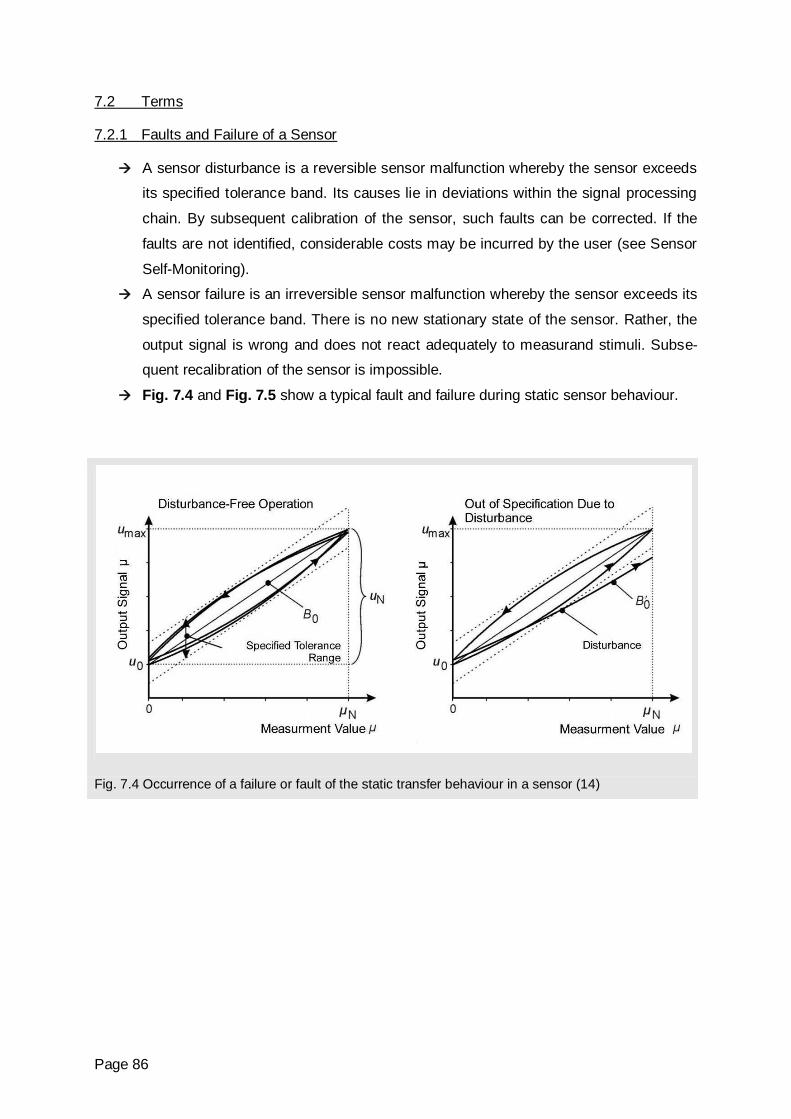
Page 86
7.2 Terms
7.2.1 Faults and Failure of a Sensor
A sensor disturbance is a reversible sensor malfunction whereby the sensor exceeds
its specified tolerance band. Its causes lie in deviations within the signal processing
chain. By subsequent calibration of the sensor, such faults can be corrected. If the
faults are not identified, considerable costs may be incurred by the user (see Sensor
Self-Monitoring).
A sensor failure is an irreversible sensor malfunction whereby the sensor exceeds its
specified tolerance band. There is no new stationary state of the sensor. Rather, the
output signal is wrong and does not react adequately to measurand stimuli. Subse-
quent recalibration of the sensor is impossible.
Fig. 7.4 and Fig. 7.5 show a typical fault and failure during static sensor behaviour.
Fig. 7.4 Occurrence of a failure or fault of the static transfer behaviour in a sensor (14)
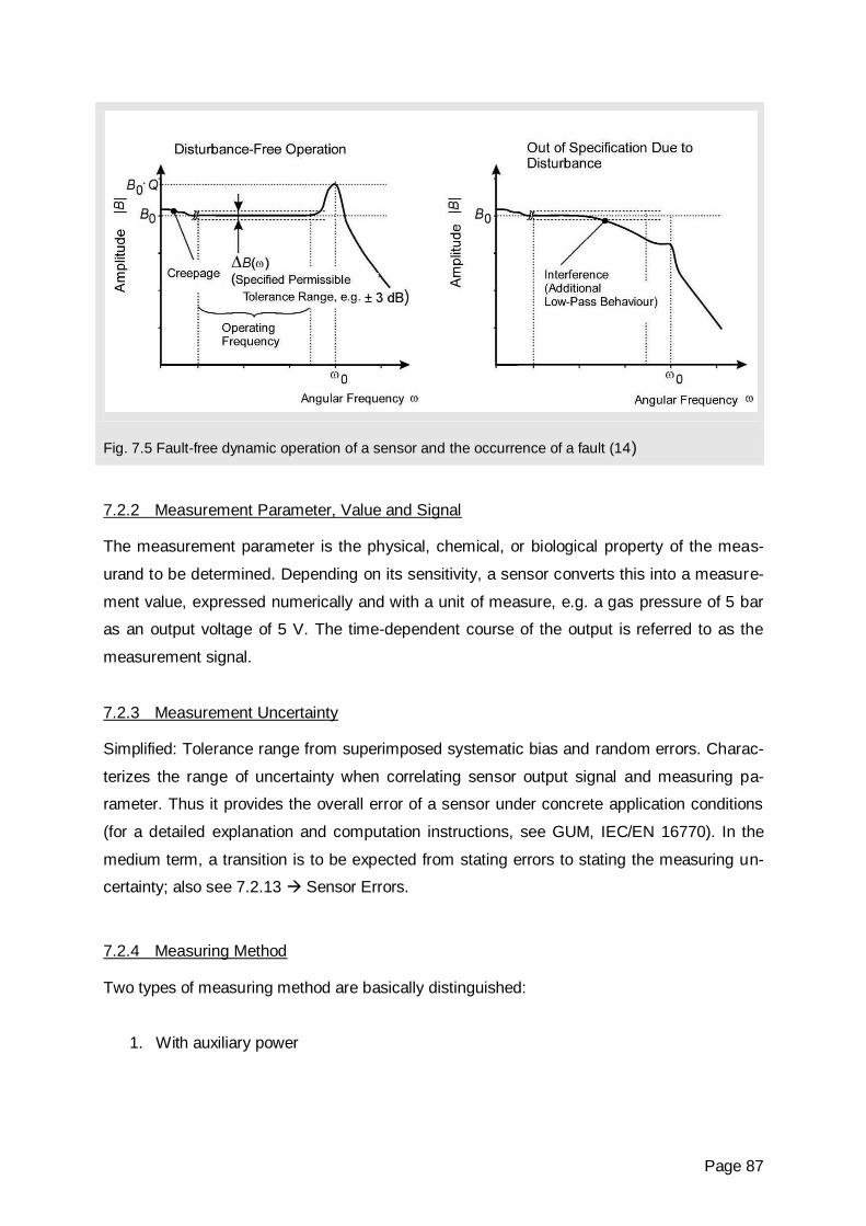
Page 87
Fig. 7.5 Fault-free dynamic operation of a sensor and the occurrence of a fault (14)
7.2.2 Measurement Parameter, Value and Signal
The measurement parameter is the physical, chemical, or biological property of the meas-
urand to be determined. Depending on its sensitivity, a sensor converts this into a measure-
ment value, expressed numerically and with a unit of measure, e.g. a gas pressure of 5 bar
as an output voltage of 5 V. The time-dependent course of the output is referred to as the
measurement signal.
7.2.3 Measurement Uncertainty
Simplified: Tolerance range from superimposed systematic bias and random errors. Charac-
terizes the range of uncertainty when correlating sensor output signal and measuring pa-
rameter. Thus it provides the overall error of a sensor under concrete application conditions
(for a detailed explanation and computation instructions, see GUM, IEC/EN 16770). In the
medium term, a transition is to be expected from stating errors to stating the measuring un-
certainty; also see 7.2.13 Sensor Errors.
7.2.4 Measuring Method
Two types of measuring method are basically distinguished:
1. With auxiliary power
Page 88
Deflection methods, e.g. capacitive, resistive, piezoresistive, magnetic, optical, induc-
tive sensor elements
Compensation methods, e.g. electrodynamic balances
Comparative methods, e.g. balances with mass pieces
Differential methods, e.g. thermocouples
Correlation methods, e.g. acoustic flowmeters
2. Without auxiliary power
Electrodynamic converters, e.g. speed sensor
Electrostatic converters, e.g. electret microphone
Piezoelectric converters, e.g. acceleration sensor
Magnetostrictive converters, e.g. torque or force sensor
7.2.5 Measuring Principle
The physical conversion principle of the sensor element, often referred to its active principle.
It describes the physical functioning by which the sensing element generates its electroni-
cally usable intermediate signal, e.g. a change in resistance, capacity, resonance frequency,
or charge, from the state to be measured (measuring parameter).
7.2.6 Measuring Process
Combination of conversion (measuring principle) and signal conditioning (measuring method)
of a sensor element.
7.2.7 Output Signal
Electrical signal obtained from the sensor secondary electronics for further processing (Fig.
7.1). May be electrical, optical, wireless, analogue or digital, and may comply with some
standard, such as 0 to 10 V, 4 to 20 mA, digital AS interference, CAN bus, Profibus etc.
7.2.8 Primary Electronics
Interface electronics for the sensor element. Invariably analogue. Describes that part of the
sensor electronics which converts the intermediate signal from the sensor element to an ana-
logue, electrical signal, including amplification, after which the signal is not as susceptible to
interference, e.g. voltage, current, or frequency. Optimizes the signal for a subsequent A/D
converter or a counting component of the digital processing electronics. For analogue condi-
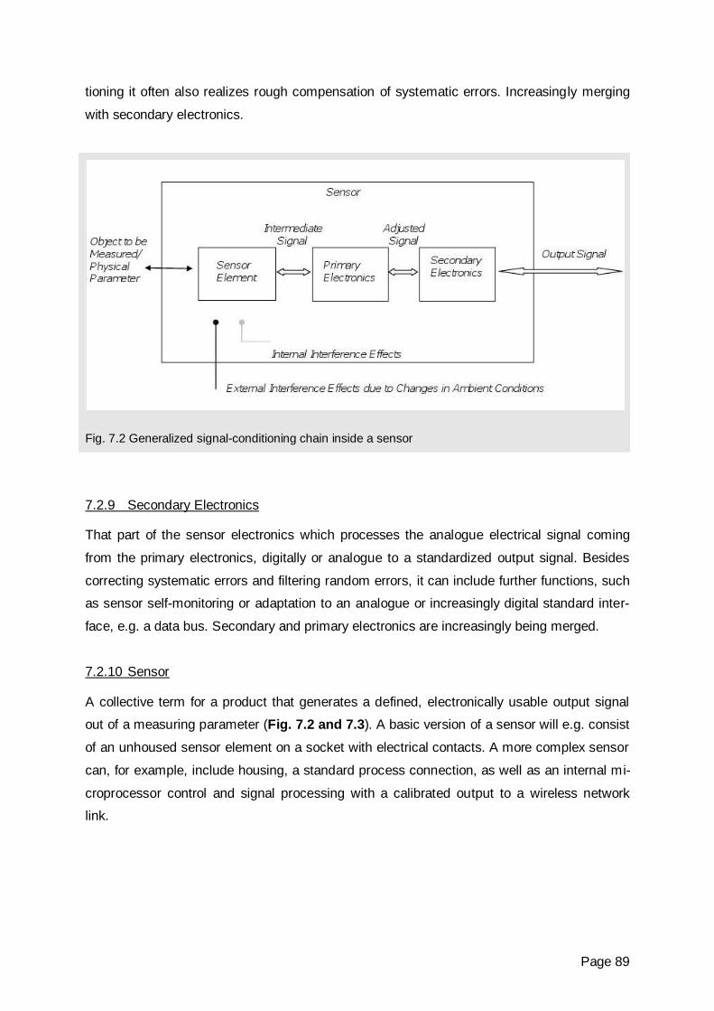
Page 89
tioning it often also realizes rough compensation of systematic errors. Increasingly merging
with secondary electronics.
Fig. 7.2 Generalized signal-conditioning chain inside a sensor
7.2.9 Secondary Electronics
That part of the sensor electronics which processes the analogue electrical signal coming
from the primary electronics, digitally or analogue to a standardized output signal. Besides
correcting systematic errors and filtering random errors, it can include further functions, such
as sensor self-monitoring or adaptation to an analogue or increasingly digital standard inter-
face, e.g. a data bus. Secondary and primary electronics are increasingly being merged.
7.2.10 Sensor
A collective term for a product that generates a defined, electronically usable output signal
out of a measuring parameter (Fig. 7.2 and 7.3). A basic version of a sensor will e.g. consist
of an unhoused sensor element on a socket with electrical contacts. A more complex sensor
can, for example, include housing, a standard process connection, as well as an internal mi-
croprocessor control and signal processing with a calibrated output to a wireless network
link.
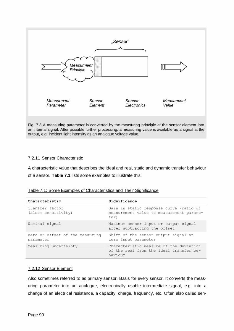
Page 90
Fig. 7.3 A measuring parameter is converted by the measuring principle at the sensor element into an internal signal. After possible further processing, a measuring value is available as a signal at the output, e.g. incident light intensity as an analogue voltage value.
7.2.11 Sensor Characteristic
A characteristic value that describes the ideal and real, static and dynamic transfer behaviour
of a sensor. Table 7.1 lists some examples to illustrate this.
Table 7.1: Some Examples of Characteristics and Their Significance
Characteristic Significance
Transfer factor
(also: sensitivity)
Gain in static response curve (ratio of
measurement value to measurement parame-
ter)
Nominal signal Maximum sensor input or output signal
after subtracting the offset
Zero or offset of the measuring
parameter
Shift of the sensor output signal at
zero input parameter
Measuring uncertainty Characteristic measure of the deviation
of the real from the ideal transfer be-
haviour
7.2.12 Sensor Element
Also sometimes referred to as primary sensor. Basis for every sensor. It converts the meas-
uring parameter into an analogue, electronically usable intermediate signal, e.g. into a
change of an electrical resistance, a capacity, charge, frequency, etc. Often also called sen-
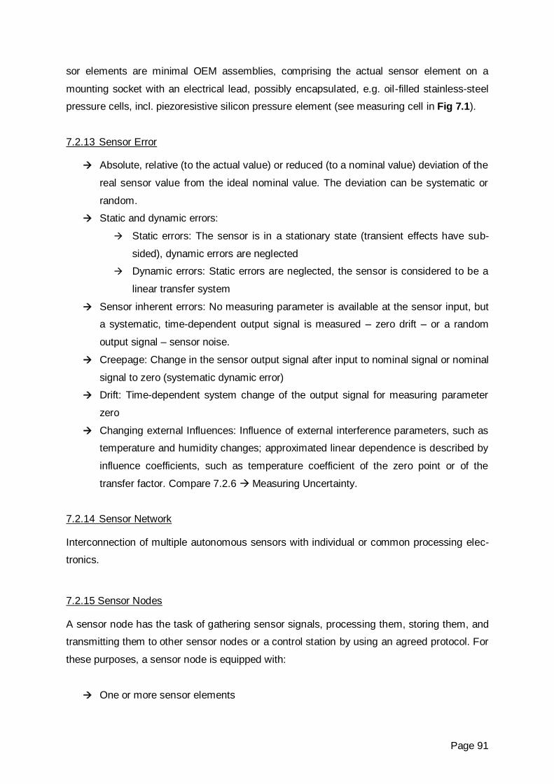
Page 91
sor elements are minimal OEM assemblies, comprising the actual sensor element on a
mounting socket with an electrical lead, possibly encapsulated, e.g. oil-filled stainless-steel
pressure cells, incl. piezoresistive silicon pressure element (see measuring cell in Fig 7.1).
7.2.13 Sensor Error
Absolute, relative (to the actual value) or reduced (to a nominal value) deviation of the
real sensor value from the ideal nominal value. The deviation can be systematic or
random.
Static and dynamic errors:
Static errors: The sensor is in a stationary state (transient effects have sub-
sided), dynamic errors are neglected
Dynamic errors: Static errors are neglected, the sensor is considered to be a
linear transfer system
Sensor inherent errors: No measuring parameter is available at the sensor input, but
a systematic, time-dependent output signal is measured – zero drift – or a random
output signal – sensor noise.
Creepage: Change in the sensor output signal after input to nominal signal or nominal
signal to zero (systematic dynamic error)
Drift: Time-dependent system change of the output signal for measuring parameter
zero
Changing external Influences: Influence of external interference parameters, such as
temperature and humidity changes; approximated linear dependence is described by
influence coefficients, such as temperature coefficient of the zero point or of the
transfer factor. Compare 7.2.6 Measuring Uncertainty.
7.2.14 Sensor Network
Interconnection of multiple autonomous sensors with individual or common processing elec-
tronics.
7.2.15 Sensor Nodes
A sensor node has the task of gathering sensor signals, processing them, storing them, and
transmitting them to other sensor nodes or a control station by using an agreed protocol. For
these purposes, a sensor node is equipped with:
One or more sensor elements

Page 92
Primary and secondary electronics
Data memory
Power supply
Wire-bound or wireless communication hardware
Necessary software
7.2.16 Sensor Reconfiguration
Sensor “repair” by which a redundantly operating sensor eliminates the deviating unit upon
self-monitoring and comparison between three or more redundant sub-units.
7.2.17 Sensor System
Integration of a number of similar sensors into a sensor array or for different measurement
parameters, into a single housing.
7.2.18 Sensor-Actuator System, Direct Coupling
Integration of sensors and actuators including relevant signal conditioning in a single compo-
nent or device.
7.2.19 Transducers and Transmitters
These are antecedent to the generic term “sensor”. Depending on the output signal and
housing, a sensor was in the past often classified as a transducer or a transmitter. The term
transducer generally designated a sensor with an uncalibrated, but possibly preamplified
signal. The term transmitter generally designated a housed sensor for industrial process con-
trol with a calibrated analogue or digital output signal suited for transmitting over a distance
of a number of metres, e.g. 4 to 20 mA, CAN bus, Profibus.
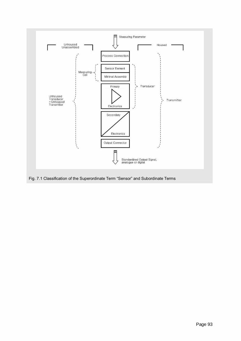
Page 93
Fig. 7.1 Classification of the Superordinate Term “Sensor” and Subordinate Terms
Page 94
8 Bibliography
1. Schröder, N.: Sensor Markets 2008, Intechno Consulting, Basel 1999. 2. Decision Etudes Conseil: European Sensor Industry: Technology, Market and Trends
2007-2011. Paris, 2008. 3. AMA Fachverband für Sensorik e.V.: Branche/Wirtschaftliche Bedeutung,
http://www.ama-sensorik.de, 2010. 4. AMA Fachverband für Sensorik e.V.: Januarumfrage 2010, http://www.ama-
sensorik.de/media/ pm_quartalsumfrage_ama_q3.pdf, 2010 5. NAMUR and VDI/VDE-GMA: Technologie-Roadmap: process-sensors 2005-2015,
Düsseldorf 2005. 6. Gassmann,O., Kottmann, J.: Technologiemanagement in der Sensorik, Wissensma-
nagement 8, 2002. 7. Jelinek, L.: Global Silicon Forecast H1 2009 Market Tracker, Silicon Manufacturers
Fall Victim to Falling Global Demands, iSuppli, http://www.isuppli.com, 2009. 8. ZMD: Mehrkanal-Sensorinterface-IC, Press release, 05. Mai 2008. 9. Mesch, F.: Struktur zur Selbstüberwachung von Meß-Systemen, Automatisierungs-
technische Praxis 08-2001. 10. Isermann, R: Fault-Diagnoses Systems, Springer Verlag, Heidelberg 2006. 11. VDI/VDE 2650: Anforderungen an Selbstüberwachung and Diagnose in der Feldin-
strumentierung, Beuth Verlag, Berlin 2006. 12. Müller, R.: Selbstüberwachung differenzdruckbasierter Durchflussmessverfahren für
Flüssigkeiten. Dissertation, TU Darmstadt 2006. 13. Müller, R., Nuber, M., Wertschützky, R.: Selbstüberwachender Durchfluss-Sensor mit
diversitärer Redundanz, Technisches Messen 71(04), 2005. 14. Werthschützky, R., Müller, R.: Selbstüberwachung and Störungstoleranz von autar-
ken sensors, Technisches Messen 74(04), 2007. 16. Frost & Sullivan: World Wireless Sensor and Transmitter Markets, 2006. 17. Lewis, F.L.: Automation and Robotics Research Institute, University of Texas at Ar-
lington. 18. Wilde, J. et al.: Hochtemperaturelektronik. Verbindungstechnik in der Elektronik, VTE
15, 2003. 19. 3D-MID e.V.: http://www.3d-mid.de/deutsch/3-d-mid-e.v./veroeffentlichungen 2009. 20. Fischer, S., Wilde, J.: Modelling package-induced effects on moulded Hall sensors,
IEEE Trans. Advanced Packaging 13/3, 2008.
Page 95
21. Fischer, S.: Einfluss der Aufbau- and Verbindungstechnik auf die funktionalen Eigen-
schaften thermomechanisch belasteter sensors, Dissertation, Albert-Ludwigs-Universität Freiburg 2006.
22. Pustan, D., Wilde, J.: Belastungsanalyse elektronischer Systeme, Technisches Mes-
sen, 75(2), 2008. 23. Löw, R.: Stress evaluation and reliability analysis of electrically conductive adhesive
interconnections, Dissertation, Albert-Ludwigs-Universität Freiburg 2009. 24. Deier, E. J.: Materialbasierte Modellierung der Genauigkeit mikromechanischer Druck
sensors, Dissertation, Albert-Ludwigs-Universität Freiburg 2008. 25. Dumas, N., Azais, F., Latorre, N., Nouet, P.: Electro-thermal stimuli for MEMS testing
in FSBM technology, Journal of electronic testing 22, 2006. 26. Beroulle, V., Bertrand, Y., Latorre, N., Nouet, P.: Test and testability of a monolithic
MEMS for magnetic field sensing, Journal of electronic testing 17, 2001. 27. Memunity – The MEMS test Community: What is on-wafer / unpackaged MEMS test-
ing? http://www.memunity.org/on-wafer_testing.htm, 2010. 29. Charlot, B., Mir, S., Parrain, F., Courtois, B.: Generation of electrically induced stimuli
for MEMS self-test, Journal of electronic testing 17, 2001. 30. Rufer, L., Mir, S., Simeu, E., Domingues, C.: On-chip pseudorandom testing, Journal
of electronic testing 21, 2005. 31. Wilde, J.: Trends in Assembly and Packaging of Sensors, Sensor 2009, 14th
International Conference, Proceedings Vol. 1, Nuremberg, Germany 2009 32. Wilde, J.: Trends in der Aufbau- and Verbindungstechnik von Mikrosystemen, Mikro-
SystemTechnik Kongress 2009, Berlin, Proceedings, VDE (Hrsg.) 2009 33. Pustan, D., Wilde, J.: Analyse von Stressfaktoren in Baugruppen der Mechatronik,
Produktion von Leiterplatten and Systemen, PLUS, Bd. 11, 2009. 34. Pustan, D., Rastjagaev, E., Wilde, J.: In situ analysis of the stress development during
fabrication process of micro-assemblies, 59th Electronic Components & Technology Conference, San Diego, California, USA, 2009.
35. Gradolph, C., Friedberger, A., Müller, G., Wilde, J.: Einflüsse von Beschleunigungs-
kräften auf einen Drucksensor, Technisches Messen 76(10) 2009. 36. Gradolph, C., Friedberger, A., Müller, G., Wilde, J.: Impact of high-g and high vibra-
tion environments on piezoresistive pressure sensor performance, Sensors and Ac-tuators A: Physical, 150(1) 2009.
37. Gradolph, C.: Mikromechanischer Drucksensor zur Charakterisierung instationärer
Strömungsverhältnisse am Hubschrauberrotorblatt, Dissertation, Albert-Ludwigs-Universität Freiburg 2009.


Sensors – the Sensory Organs of Technology …
… provide safety,… save lives, … and improve our quality of life.
… protect our environment,