Embed Size (px)
Citation preview
Diplomarbeit
Characterization of IntegratedLumped Inductorsand Transformers
Ausgefuhrt zum Zwecke der Erlangung des akademischen Grades eines
Diplom-Ingenieurs unter Leitung von
Werner Simburger und Arpad L. Scholtz
E389
Institut fur Nachrichtentechnik und Hochfrequenztechnik
eingereicht an der Technischen Universitat Wien
Fakultat fur Elektrotechnik
von
Ronald Thuringer
9326356Pretschgasse 21, 1110 Wien
Wien, im April 2002

Abstract
The modern semiconductor industry has put great demands on circuit design-ers for smaller and cheaper integrated circuits. Simultaneous to this operatingfrequencies of the applications increase. An option which helps to satisfy theserequirements is the use of on-chip inductors and transformers. These elementsallow greatly improved levels of performance in bipolar and CMOS integratedcircuits.
In order to achieve best performance it is an essential task for the IC designerto predict and optimize the electrical characteristics of the inductors and trans-formers. This could be done by 3-D electromagnetic field simulation programs.But usually such simulations require very intensive computer calculations whichtake a few hours to days. Therefore it is not possible to optimize the device in areasonable amount of time.
In this thesis techniques are introduced which allow a characterization of in-ductors and transformers within a few minutes. The short calculation time isachieved by using electrical lumped low-order models. The parameters of themodel are extracted from the geometrical structure of the inductor or trans-former by using FEM-Tools and analytical considerations. These techniques havebeen compiled in a user-friendly software program FastTrafo v3.2.
FastTrafo v3.2 provides the circuit designer a powerful environment to designinductors or transformers on demand. The software delivers SPICE models basedon the technology and geometrical dimensions of the device. A verification ofthe models shows a good agreement with several test objects. An inductor and atransformer example are presented in this work.

Contents
1 Introduction 1
2 Modeling 52.1 Physical Layout . . . . . . . . . . . . . . . . . . . . . . . . . . . . 52.2 Physical Model . . . . . . . . . . . . . . . . . . . . . . . . . . . . 72.3 Low-Order Inductor Model . . . . . . . . . . . . . . . . . . . . . . 72.4 Higher-Order Inductor Model . . . . . . . . . . . . . . . . . . . . 92.5 Transformer Model . . . . . . . . . . . . . . . . . . . . . . . . . . 9
3 Parameter Extraction 133.1 Inductance Calculation . . . . . . . . . . . . . . . . . . . . . . . . 133.2 Serial Resistance . . . . . . . . . . . . . . . . . . . . . . . . . . . 153.3 Substrate Resistance . . . . . . . . . . . . . . . . . . . . . . . . . 173.4 Substrate Capacitance . . . . . . . . . . . . . . . . . . . . . . . . 203.5 Oxide and Interwinding Capacitance . . . . . . . . . . . . . . . . 213.6 Test-Structures and De-embedding . . . . . . . . . . . . . . . . . 27
4 Experimental Results 314.1 A 4.7nH Inductor for 2 GHz . . . . . . . . . . . . . . . . . . . . . 314.2 A 3:2 Transformer for 5.8 GHz . . . . . . . . . . . . . . . . . . . 38
5 Conclusion 45
A FastTrafo User Manual 47
Bibliography 75
Acknowledgements 77
i

Chapter 1
Introduction
Today monolithic inductors and transformers are used extensively in differenttypes of integrated RF circuits. Incipiently in earlier days they were realized asdiscrete components. But with the increasing demands on the application sidemore and more monolithic integrated inductors and transformers have been usedfor circuit design. This technique allows a realization of compact high frequencycircuits with a high level of integration and low production costs.
Such typical applications of integrated inductors and transformers include forexample:
• input and output matching networks for amplifiers
• inductive loaded amplifiers
• LC tank circuits of low phase noise voltage control oscillators
• BALUN function in differential applications
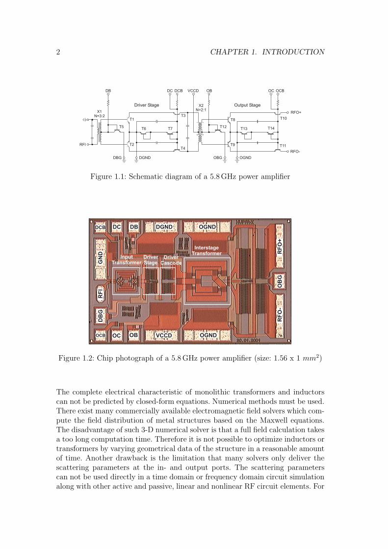
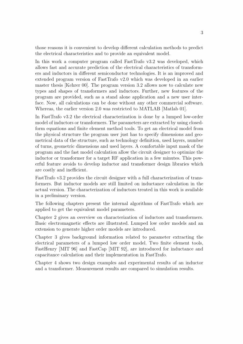
Figure 1.1 and Fig. 1.2 show the schematic diagram and micrograph of a 5.8 GHzpower amplifier realized in a 25 GHz fT silicon technology. The circuit demon-strates an application of on-chip transformers.
The circuit consists of an input transformer X1, a driver stage with cascode, aninterstage transformer X2 and an output stage with cascode. The input trans-former X1 acts as balun as well as input matching network. The balun functionallows that the input signal can be applied balanced or single ended if one inputterminal is grounded. The transformer X2 acts as interstage matching network.
Basically all integrated components show a non ideal electrical behaviour. Theyare afflicted with parasitic effects, especially the transformers. The ability to de-sign the circuits with optimum performance involves how to handle these parasiticeffects. The parasitics must be taken into consideration very careful. Therefore itis necessary to characterize the components.
1
2 CHAPTER 1. INTRODUCTION
X1N=3:2
Driver Stage Output Stage
T1 T8
T5 T12T6 T13T7 T14
T3T10
T4T11T2 T9
X2N=2:1
DB
DBG DGND OBG OGND
DC DCB VCCD OB OCB
RFO+
RFO-
OC
RFI
Figure 1.1: Schematic diagram of a 5.8 GHz power amplifier
DCB
OCB
DC
OC
DB DGND
VCCD
OGND
OGND
RF
O+
RF
O-
OB
G
GN
DR
FI
DB
G
OB
InputTransformer
InterstageTransformer
DriverStage
DriverCascode
Figure 1.2: Chip photograph of a 5.8 GHz power amplifier (size: 1.56 x 1 mm2)
The complete electrical characteristic of monolithic transformers and inductorscan not be predicted by closed-form equations. Numerical methods must be used.There exist many commercially available electromagnetic field solvers which com-pute the field distribution of metal structures based on the Maxwell equations.The disadvantage of such 3-D numerical solver is that a full field calculation takesa too long computation time. Therefore it is not possible to optimize inductors ortransformers by varying geometrical data of the structure in a reasonable amountof time. Another drawback is the limitation that many solvers only deliver thescattering parameters at the in- and output ports. The scattering parameterscan not be used directly in a time domain or frequency domain circuit simulationalong with other active and passive, linear and nonlinear RF circuit elements. For
3
those reasons it is convenient to develop different calculation methods to predictthe electrical characteristics and to provide an equivalent model.
In this work a computer program called FastTrafo v3.2 was developed, whichallows fast and accurate prediction of the electrical characteristics of transform-ers and inductors in different semiconductor technologies. It is an improved andextended program version of FastTrafo v2.0 which was developed in an earliermaster thesis [Kehrer 00]. The program version 3.2 allows now to calculate newtypes and shapes of transformers and inductors. Further, new features of theprogram are provided, such as a stand alone application and a new user inter-face. Now, all calculations can be done without any other commercial software.Whereas, the earlier version 2.0 was restricted to MATLAB [Matlab 01].
In FastTrafo v3.2 the electrical characterization is done by a lumped low-ordermodel of inductors or transformers. The parameters are extracted by using closed-form equations and finite element method tools. To get an electrical model fromthe physical structure the program user just has to specify dimensions and geo-metrical data of the structure, such as technology definition, used layers, numberof turns, geometric dimensions and used layers. A comfortable input mask of theprogram and the fast model calculation allow the circuit designer to optimize theinductor or transformer for a target RF application in a few minutes. This pow-erful feature avoids to develop inductor and transformer design libraries whichare costly and inefficient.
FastTrafo v3.2 provides the circuit designer with a full characterization of trans-formers. But inductor models are still limited on inductance calculation in theactual version. The characterization of inductors treated in this work is availablein a preliminary version.
The following chapters present the internal algorithms of FastTrafo which areapplied to get the equivalent model parameters.
Chapter 2 gives an overview on characterization of inductors and transformers.Basic electromagnetic effects are illustrated. Lumped low order models and anextension to generate higher order models are introduced.
Chapter 3 gives background information related to parameter extracting theelectrical parameters of a lumped low order model. Two finite element tools,FastHenry [MIT 96] and FastCap [MIT 92], are introduced for inductance andcapacitance calculation and their implementation in FastTrafo.
Chapter 4 shows two design examples and experimental results of an inductorand a transformer. Measurement results are compared to simulation results.

4 CHAPTER 1. INTRODUCTION
Chapter 2
Modeling
In this chapter equivalent models of planar inductors and transformers are de-rived from the physical layout. The treatment starts with a short overview ofthe physical effects. Afterwards appropriate equivalent electrical models are in-troduced.
2.1 Physical Layout
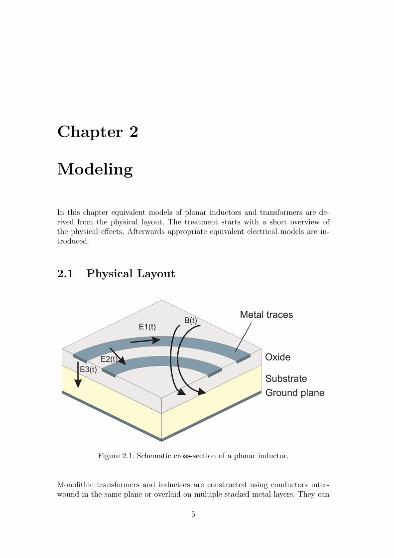
Figure 2.1: Schematic cross-section of a planar inductor.
Monolithic transformers and inductors are constructed using conductors inter-wound in the same plane or overlaid on multiple stacked metal layers. They can
5
6 CHAPTER 2. MODELING
be implemented in circular or rectangular shapes with different winding configu-rations. Each of these realizations shows specific performance advantages. Thereexist many publications which describe these possibilities in construction andoptimization of inductors [Ashby 96], [Yue 98], [Niknejad 00] and transformers[Rabjohn 89], [Long 00].
Independent on their geometrical structures there affect always the same physicalphenomena on the structures. Figure 2.1 shows a schematic three dimensionalcross-section of an inductor. It gives an insight into the basic physical effects. Thepicture shows only two adjacent turns realized on one metal layer embedded inoxide. The conductors are separated from the substrate by oxide. This simplifiedmodel is sufficient to illustrate the different electromagnetic fields that are presentin an integrated inductor when excited.
Around the traces exists a time varying magnetic field B(t), created by the cur-rent flow in the metal. B(t) is responsible for the stored magnetic energy andthe resulting inductance. Further, in case of transformers B(t) is responsible forcoupling between the primary and secondary winding.
Unfortunately there also exist other electromagnetic fields that decrease the per-formance of inductors and transformers which result in losses produced due tothe non ideal physical properties of the used materials. Each of the electric fieldcomponents E1-E3 in Fig.2.1 results in loss of energy in the whole structure.E1(t) is the electric field along the metal trace. It is caused by the current inthe winding and the finite conductivity. The current causes in association withohmic losses a voltage drop along the whole winding. It arises a voltage differencebetween each turn. This difference maintains the field denoted by E2(t) which ispresent between each turn. Due to the finite resistance and capacitive couplinga leakage current flows from turn to turn. In the same manner the electric fieldcomponent E3(t) forces a leakage current between the metal traces and ground.
In addition to the described electromagnetic fields, many other high-order effectsare present. For instance, eddy currents arise in the metal traces and force a skineffect due to penetration of time varying magnetic fields. Further a proximityeffect occurs due to the interaction between the magnetic field and currents.Both results in increased resistances and losses. Additionally currents inducedin the substrate give rise to counterproductive secondary magnetic fields whichinteract with the primary magnetic field B(t).
CHAPTER 2. MODELING 7
2.2 Physical Model
An alternative to a fully 3-D field analysis is an approximation with electricallumped elements (R,L,C). This is valid because the physical lengths of the con-ducting segments in the layout are typically much less than the guided wavelengthat the operation frequency. In order to this approximation the analysis is reducedto electrostatic and magnetostatic calculations for easier treatment.
In a physical model each circuit element is related directly to the physical layout.This property is very important when designing new inductors or transformerswhere measurements data are not available.
The key to accurate physical modeling in this way is the ability to describe thebehaviour of the inductance and the parasitic effects. Each lumped element ofthe model should be consistent with the physical phenomena occuring in thepart of structure it represents. In a pure physical model the value of electricallumped elements is only determined by the geometry and material constants ofthe structure.
At modeling we have to make a decision about the accuracy and limitations of themodel. The integration of several lumped elements gives only an estimation of theelectrical behaviour. It is clear that the number of elements determines the gradeof the approximation. With increasing number of elements the precision increases.On the other hand the simulation time rises too. A compromise between accuracyand simulation time has to be done.
2.3 Low-Order Inductor Model
The aim of low-order models is to reduce the number of parts in the equivalentcircuit to a minimum. The following proposed low-order model allows a charac-terization of the inductor up to its first self resonant frequency. Near and abovethe self resonant frequency the model fails due to the low-order.
The basic idea is to model the whole winding as one lumped physical elementwith two ports. Accordingly, the inductance and all parasitics just relate to onephysical element.
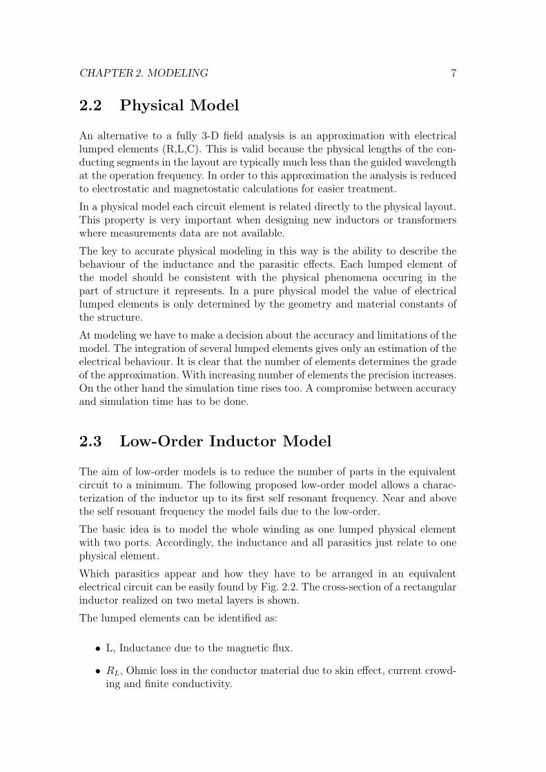
Which parasitics appear and how they have to be arranged in an equivalentelectrical circuit can be easily found by Fig. 2.2. The cross-section of a rectangularinductor realized on two metal layers is shown.
The lumped elements can be identified as:
• L, Inductance due to the magnetic flux.
• RL, Ohmic loss in the conductor material due to skin effect, current crowd-ing and finite conductivity.
8 CHAPTER 2. MODELING
C R
COx
Sub Sub
CL
LRL
Substrate
Oxide
P-
P+
TopviewMetal layer 2Metal layer 1
Ground plane
Figure 2.2: Three dimensional cross-section of a monolithic inductor
• CL, Parasitic capacitive coupling between the winding turns.
• CSub, Parasitic capacitive coupling into the substrate.
• COx, Parasitic capacitive coupling into the oxide.
• RSub, Ohmic loss in the conductive substrate.
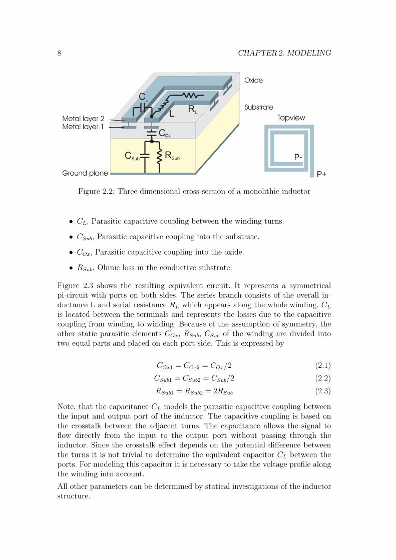
Figure 2.3 shows the resulting equivalent circuit. It represents a symmetricalpi-circuit with ports on both sides. The series branch consists of the overall in-ductance L and serial resistance RL which appears along the whole winding. CL
is located between the terminals and represents the losses due to the capacitivecoupling from winding to winding. Because of the assumption of symmetry, theother static parasitic elements COx, RSub, CSub of the winding are divided intotwo equal parts and placed on each port side. This is expressed by
COx1 = COx2 = COx/2 (2.1)
CSub1 = CSub2 = CSub/2 (2.2)
RSub1 = RSub2 = 2RSub (2.3)
Note, that the capacitance CL models the parasitic capacitive coupling betweenthe input and output port of the inductor. The capacitive coupling is based onthe crosstalk between the adjacent turns. The capacitance allows the signal toflow directly from the input to the output port without passing through theinductor. Since the crosstalk effect depends on the potential difference betweenthe turns it is not trivial to determine the equivalent capacitor CL between theports. For modeling this capacitor it is necessary to take the voltage profile alongthe winding into account.
All other parameters can be determined by statical investigations of the inductorstructure.
CHAPTER 2. MODELING 9
CL
RL
RSub2
CCSub2
RSub1
CSub1
LC
Ox1 COx2
P+ P-
Figure 2.3: Compact inductor model
2.4 Higher-Order Inductor Model
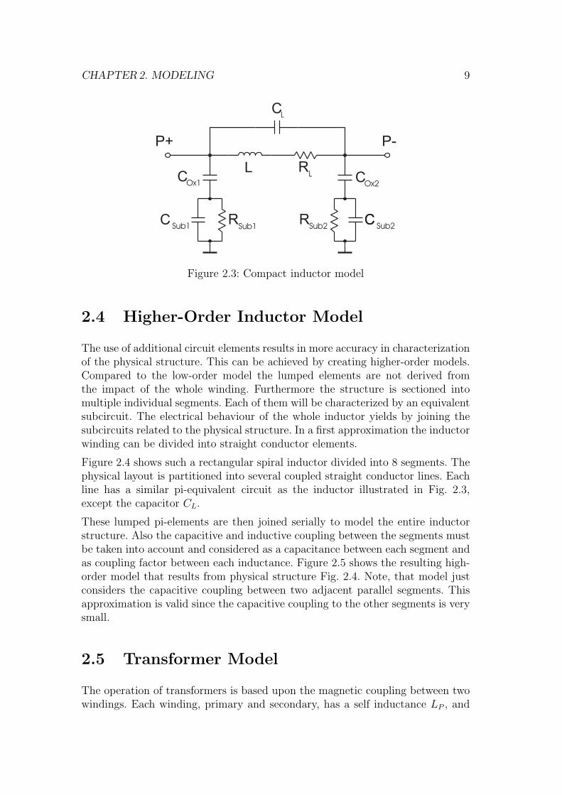
The use of additional circuit elements results in more accuracy in characterizationof the physical structure. This can be achieved by creating higher-order models.Compared to the low-order model the lumped elements are not derived fromthe impact of the whole winding. Furthermore the structure is sectioned intomultiple individual segments. Each of them will be characterized by an equivalentsubcircuit. The electrical behaviour of the whole inductor yields by joining thesubcircuits related to the physical structure. In a first approximation the inductorwinding can be divided into straight conductor elements.
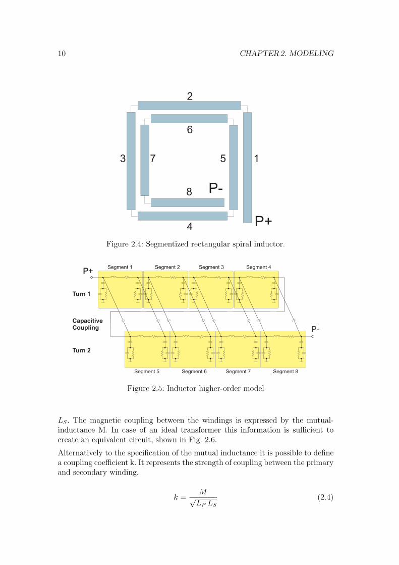
Figure 2.4 shows such a rectangular spiral inductor divided into 8 segments. Thephysical layout is partitioned into several coupled straight conductor lines. Eachline has a similar pi-equivalent circuit as the inductor illustrated in Fig. 2.3,except the capacitor CL.
These lumped pi-elements are then joined serially to model the entire inductorstructure. Also the capacitive and inductive coupling between the segments mustbe taken into account and considered as a capacitance between each segment andas coupling factor between each inductance. Figure 2.5 shows the resulting high-order model that results from physical structure Fig. 2.4. Note, that model justconsiders the capacitive coupling between two adjacent parallel segments. Thisapproximation is valid since the capacitive coupling to the other segments is verysmall.
2.5 Transformer Model
The operation of transformers is based upon the magnetic coupling between twowindings. Each winding, primary and secondary, has a self inductance LP , and
10 CHAPTER 2. MODELING
P+
P-
6
4
2
7 13 5
8
Figure 2.4: Segmentized rectangular spiral inductor.
P+P+
P-
Segment 1 Segment 2 Segment 3 Segment 4
Segment 5 Segment 6 Segment 7 Segment 8
Turn 2
Turn 1
CapacitiveCoupling
Figure 2.5: Inductor higher-order model
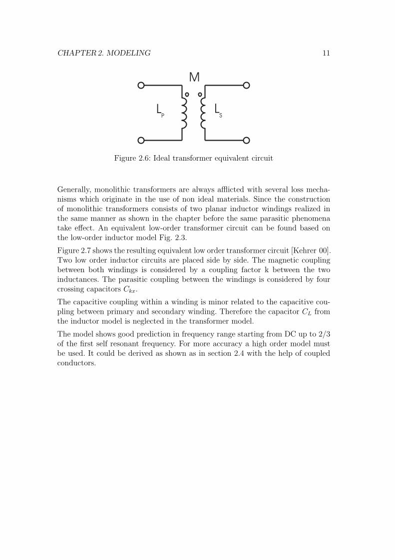
LS. The magnetic coupling between the windings is expressed by the mutual-inductance M. In case of an ideal transformer this information is sufficient tocreate an equivalent circuit, shown in Fig. 2.6.
Alternatively to the specification of the mutual inductance it is possible to definea coupling coefficient k. It represents the strength of coupling between the primaryand secondary winding.
k =M√
LP LS
(2.4)
CHAPTER 2. MODELING 11
LP
LS
M
Figure 2.6: Ideal transformer equivalent circuit
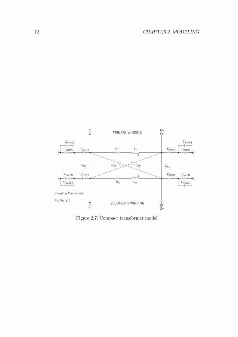
Generally, monolithic transformers are always afflicted with several loss mecha-nisms which originate in the use of non ideal materials. Since the constructionof monolithic transformers consists of two planar inductor windings realized inthe same manner as shown in the chapter before the same parasitic phenomenatake effect. An equivalent low-order transformer circuit can be found based onthe low-order inductor model Fig. 2.3.
Figure 2.7 shows the resulting equivalent low order transformer circuit [Kehrer 00].Two low order inductor circuits are placed side by side. The magnetic couplingbetween both windings is considered by a coupling factor k between the twoinductances. The parasitic coupling between the windings is considered by fourcrossing capacitors Ckx.
The capacitive coupling within a winding is minor related to the capacitive cou-pling between primary and secondary winding. Therefore the capacitor CL fromthe inductor model is neglected in the transformer model.
The model shows good prediction in frequency range starting from DC up to 2/3of the first self resonant frequency. For more accuracy a high order model mustbe used. It could be derived as shown as in section 2.4 with the help of coupledconductors.
12 CHAPTER 2. MODELING
PRIMARY WINDING
SECONDARY WINDING
P-
S-
P+
S+
LRC
CC CC
R
R C
R L
C R
C R
Coupling Coefficient:
k (L ,L )
SubP2
SubS2
SubP1
SubS1
OXP1
OXS1
OXP2
OXS2
K4 K3 K2
P
S
P
S
K1
P SPS
CSubP2 CSubP1
CSubS1CSubS2
Figure 2.7: Compact transformer model
Chapter 3
Parameter Extraction
A lumped low-order model for inductors and transformers is found in chapter2. This chapter describes the parameter extraction method from the physicalstructure.
3.1 Inductance Calculation
Inductance calculation of metal structures is based on the Maxwell equation.
× H = J + ∂tD (3.1)
With this formula it is possible to derive an inductance value for arbitrary 3-Dstructures. Unfortunately in most cases it does not exist a closed form expression.Therefore numerical methods must be used to solve the problem in this way.
In our applications generally the frequencies of interest are quite low to reduce theproblem to a magnetoquasistatic analysis. This assumption leads to inductanceexpressions for coils and transformers which can be easily attained from knownbasic inductance formulas. In [Kehrer 00] it is shown step by step how to get thisresulting expression starting from the magnetoquasistatic approximation.
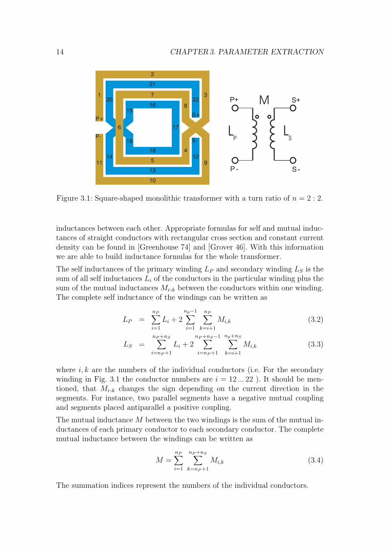
The result is that each transformer or inductor can be analyzed alone with knowl-edge of the self- and mutual inductances of individual conductor elements. Figure3.1 shows a transformer with a turn ratio of n=2:2. The transformer structure canbe interpreted as a composition of several rectilinear conductors. The individualconductor elements are consecutively numbered from 1 to 22. The trace with theelements 1-11 represents the primary winding which consists of two turns. Onthe left side is the primary port labeled with P+ and P-. The secondary windingbegins on the right side with the conductor element 12 and ends with element 22.The secondary port is labelled with S+ and S-.
After splitting the transformer into a sequence of rectilinear conductors it is neces-sary to get information about the self inductances from each segment and mutual
13
14 CHAPTER 3. PARAMETER EXTRACTION
Figure 3.1: Square-shaped monolithic transformer with a turn ratio of n = 2 : 2.
inductances between each other. Appropriate formulas for self and mutual induc-tances of straight conductors with rectangular cross section and constant currentdensity can be found in [Greenhouse 74] and [Grover 46]. With this informationwe are able to build inductance formulas for the whole transformer.
The self inductances of the primary winding LP and secondary winding LS is thesum of all self inductances Li of the conductors in the particular winding plus thesum of the mutual inductances Mi,k between the conductors within one winding.The complete self inductance of the windings can be written as
LP =nP∑i=1
Li + 2np−1∑i=1
nP∑k=i+1
Mi,k (3.2)
LS =nP +nS∑i=nP +1
Li + 2nP +nS−1∑i=nP +1
np+nS∑k=i+1
Mi,k (3.3)
where i, k are the numbers of the individual conductors (i.e. For the secondarywinding in Fig. 3.1 the conductor numbers are i = 12 ... 22 ). It should be men-tioned, that Mi,k changes the sign depending on the current direction in thesegments. For instance, two parallel segments have a negative mutual couplingand segments placed antiparallel a positive coupling.
The mutual inductance M between the two windings is the sum of the mutual in-ductances of each primary conductor to each secondary conductor. The completemutual inductance between the windings can be written as
M =nP∑i=1
nP +nS∑k=nP +1
Mi,k (3.4)
The summation indices represent the numbers of the individual conductors.
CHAPTER 3. PARAMETER EXTRACTION 15
This approach to calculate the overall inductance by summing the inductancesfrom joined wire segments can be found in the literature called as Greenhousemethod [Greenhouse 74]. It is applicable as long as there exists self inductanceand mutual inductance expressions for the single segments. This is not a limitationin our applications since the geometries of planar transformers and inductors arebased on rectangle- or polygon-shape turns which always consist of rectilinearconductors.
A similar algorithm in a more complex form is realized in the freeware programFastHenry. FastHenry [MIT 96] is a program capable to compute self and mutualinductances of arbitrary tridimensional conductive structures in a magnetoqua-sistatic approximation. The algorithm used in FastHenry is an acceleration of amesh formulation approach. The internal resulting linear system from the meshformulation is solved using a generalized minimal residual algorithm with a fastmultipole algorithm to efficiently compute the problem. This allows a very shortcalculation time. The user just has to specify an input file where the conduc-tors are defined as a sequence of rectilinear segments. The current distributionin the structure will automatically be calculated by the program with the helpof the created meshes. Therefore the signs of the calculated mutual inductanceare always correctly assigned. Hence the user is only constrained to handle thephysical dimensions and not to take care on the current flow direction in eachsegment. The resulting self and mutual inductance values relate on user definedinput ports. These terminals may be set by the user at any places along the metalstructure.
Because of short processing time and easy handling of the conductor elements,FastHenry is ideally suitable for our applications. These advantages are decisiveof preferring the freeware program instead to of writing an own Greenhouse al-gorithm in the software core of FastTrafo. FastTrafo provides to you an interfacefor generating appropriate FastHenry input files which describe the transformeror inductor structures.
3.2 Serial Resistance
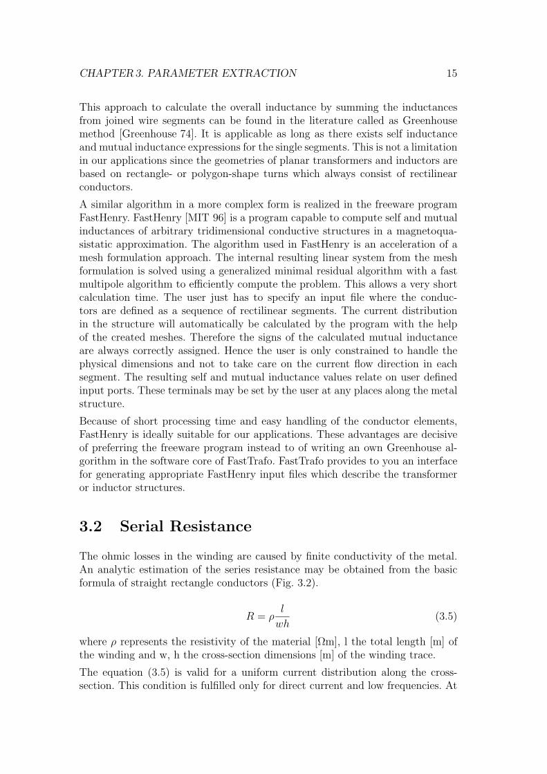
The ohmic losses in the winding are caused by finite conductivity of the metal.An analytic estimation of the series resistance may be obtained from the basicformula of straight rectangle conductors (Fig. 3.2).
R = ρl
wh(3.5)
where ρ represents the resistivity of the material [Ωm], l the total length [m] ofthe winding and w, h the cross-section dimensions [m] of the winding trace.
The equation (3.5) is valid for a uniform current distribution along the cross-section. This condition is fulfilled only for direct current and low frequencies. At
16 CHAPTER 3. PARAMETER EXTRACTION
Figure 3.2: Straight rectangular conductor
increasing frequencies the current density becomes more and more nonuniformdue to high frequency effects in the metal. They can by identified as skin andproximity effect. The origin of both lies in penetration of time varying magneticfields in the metal.
At the skin effect the magnetic field in the metal is produced by the current flowin the conductor itself. The induced eddy currents in the conductor force most ofthe current to flow near the boundary of the metal conductor. In consequence ofthe higher current density on the edges, the serial resistance increases with thefrequency. A formula for the high frequency resistance in rectangle conductors(Fig. 3.2) based on the direct current case was given by [Lofti 95].
RAC = RDC
1 +
(f
fl
)2
+
(f
fu
)5
110
(3.6)
fl =πρ
2µwh, fu =
π2ρ
µh2
K
√1 − h2
w2
−2
(3.7)
where w, h are the cross-section dimensions [m], µ is the permeability [Vs/Am] ofthe metal. RDC is the resistance [Ω] in the direct current mode. The frequenciesfl and fu [Hz] are the cutting frequencies of the low frequency case and of thehigh frequency case. K is the elliptic integral first order
K(x) =∫ π
2
0
1√1 − x2 sin2(φ)
dφ (3.8)
In contrast to the skin effect, the proximity effect only occurs if at least two con-ductors are present. The magnetic fields from each conductor affects the currentflow in the other, resulting in a non-uniform current distribution. The proximityeffect is similar to the skin effect. The effective cross-sectional area of the con-ductor is decreased and in order to this the resistance is increased. For this case
CHAPTER 3. PARAMETER EXTRACTION 17
the mathematical problem is significantly more complex due to the interactionof the second or more conductors. It is not possible to solve the problem with aclosed formula as it is possible for the skin effect. Therefore numerical methodsmust be used.
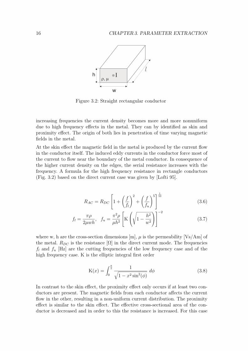
In FastTrafo the serial resistance is calculated by the program FastHenry [MIT 96].In addition to the inductances between defined terminals the software delivers theeffective serial resistances. The internal used algorithm is based on (3.5) whichassumes a uniform current density along the cross-section. However, it is possibleto take the skin and proximity effect into account. The whole cross-section of theconductor is divided into a bundle of rectangle filaments (Fig. 3.3). The currentdensity inside each filament is assumed to be constant but the magnitude maydiffer from filament to filament. An iterative algorithm considers the interactionbetween the magnetic fields produced by each filament and the current in eachfilament. The result is an approximation of the current distribution through abundle of filaments where each sustains a constant current density. With thisdiscretized current distribution and formula (3.5) it is possible for the programto evaluate the equivalent series resistance of the whole conductor.
I
Figure 3.3: Conductor discretization into a bundle of filaments
It is evident that the accuracy of the approximation depends on the number ofdiscretized elements. But it should be mentioned that there exists a trade offbetween the accuracy and processing time of the calculation.
3.3 Substrate Resistance
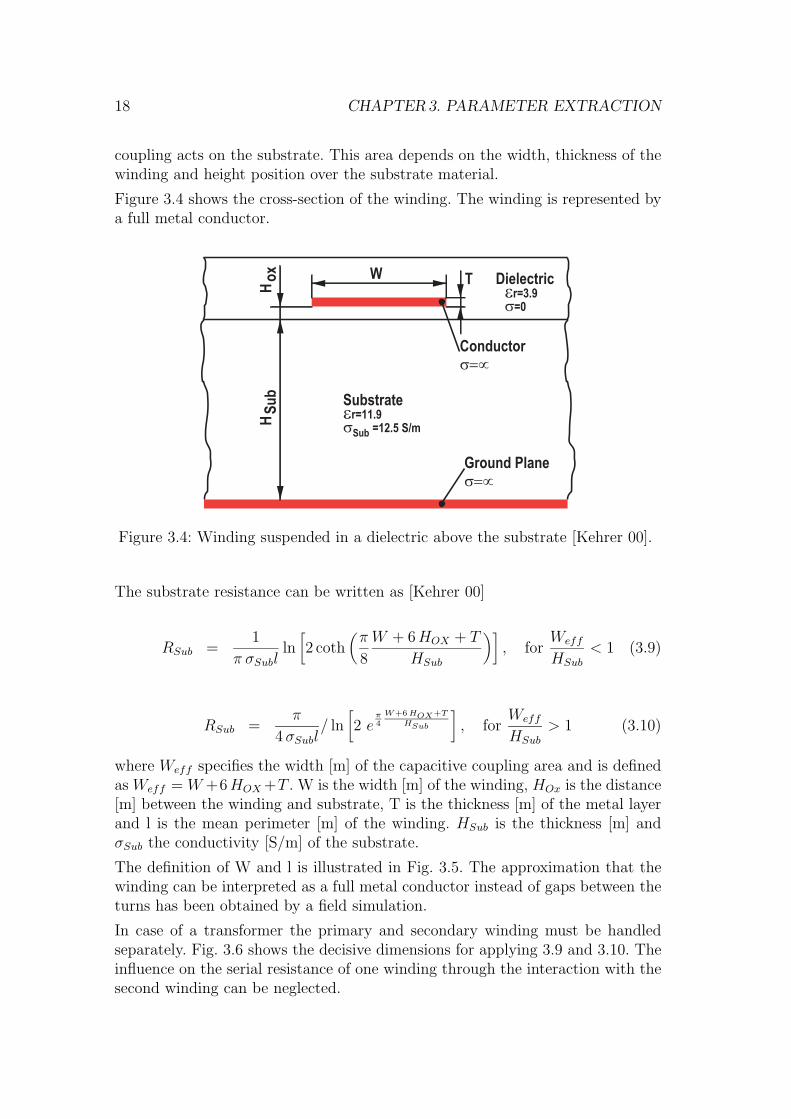
The substrate resistance represents the ohmic losses in the substrate. They arecaused by the current flow between the winding conductor and the ground con-tact. Although the winding is embedded in a non-conducting dielectric a currentflow is possible through the capacitive coupling between winding and substrate.
An appropriate expression for the substrate resistance is derived in [Kehrer 00].The substrate resistance calculation is based on the area where the capacitive
18 CHAPTER 3. PARAMETER EXTRACTION
coupling acts on the substrate. This area depends on the width, thickness of thewinding and height position over the substrate material.
Figure 3.4 shows the cross-section of the winding. The winding is represented bya full metal conductor.
Figure 3.4: Winding suspended in a dielectric above the substrate [Kehrer 00].
The substrate resistance can be written as [Kehrer 00]
RSub =1
π σSublln
[2 coth
(π
8
W + 6 HOX + T
HSub
)], for
Weff
HSub
< 1 (3.9)
RSub =π
4 σSubl/ ln
[2 e
π4
W+6 HOX+T
HSub
], for
Weff
HSub
> 1 (3.10)
where Weff specifies the width [m] of the capacitive coupling area and is definedas Weff = W +6 HOX +T . W is the width [m] of the winding, HOx is the distance[m] between the winding and substrate, T is the thickness [m] of the metal layerand l is the mean perimeter [m] of the winding. HSub is the thickness [m] andσSub the conductivity [S/m] of the substrate.
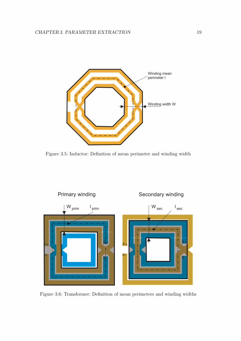
The definition of W and l is illustrated in Fig. 3.5. The approximation that thewinding can be interpreted as a full metal conductor instead of gaps between theturns has been obtained by a field simulation.
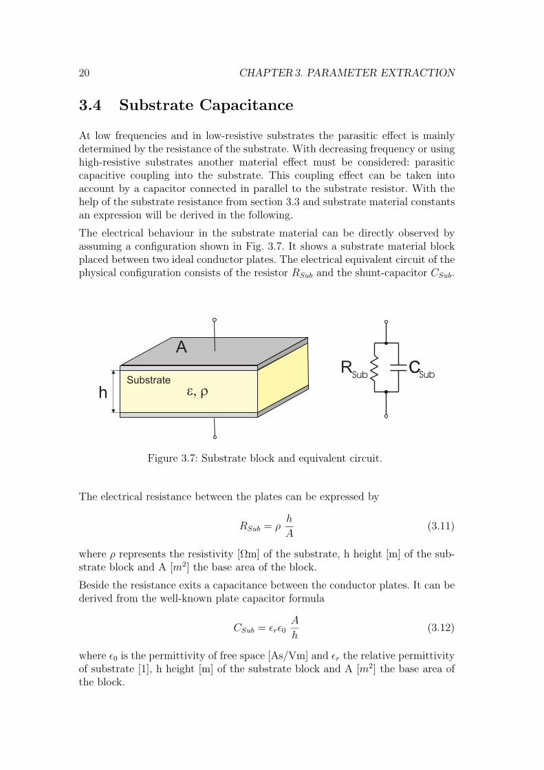
In case of a transformer the primary and secondary winding must be handledseparately. Fig. 3.6 shows the decisive dimensions for applying 3.9 and 3.10. Theinfluence on the serial resistance of one winding through the interaction with thesecond winding can be neglected.
CHAPTER 3. PARAMETER EXTRACTION 19
Winding meanperimeter l
Winding width W
Figure 3.5: Inductor: Definition of mean perimeter and winding width
W
Primary winding Secondary winding
prim l prim W sec l sec
Figure 3.6: Transformer: Definition of mean perimeters and winding widths
20 CHAPTER 3. PARAMETER EXTRACTION
3.4 Substrate Capacitance
At low frequencies and in low-resistive substrates the parasitic effect is mainlydetermined by the resistance of the substrate. With decreasing frequency or usinghigh-resistive substrates another material effect must be considered: parasiticcapacitive coupling into the substrate. This coupling effect can be taken intoaccount by a capacitor connected in parallel to the substrate resistor. With thehelp of the substrate resistance from section 3.3 and substrate material constantsan expression will be derived in the following.
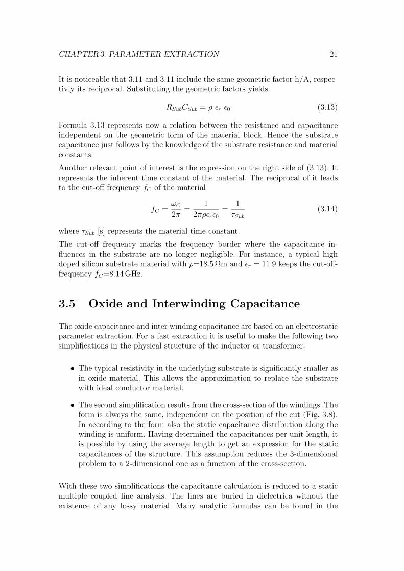
The electrical behaviour in the substrate material can be directly observed byassuming a configuration shown in Fig. 3.7. It shows a substrate material blockplaced between two ideal conductor plates. The electrical equivalent circuit of thephysical configuration consists of the resistor RSub and the shunt-capacitor CSub.
Figure 3.7: Substrate block and equivalent circuit.
The electrical resistance between the plates can be expressed by
RSub = ρh
A(3.11)
where ρ represents the resistivity [Ωm] of the substrate, h height [m] of the sub-strate block and A [m2] the base area of the block.
Beside the resistance exits a capacitance between the conductor plates. It can bederived from the well-known plate capacitor formula
CSub = εrε0A
h(3.12)
where ε0 is the permittivity of free space [As/Vm] and εr the relative permittivityof substrate [1], h height [m] of the substrate block and A [m2] the base area ofthe block.
CHAPTER 3. PARAMETER EXTRACTION 21
It is noticeable that 3.11 and 3.11 include the same geometric factor h/A, respec-tivly its reciprocal. Substituting the geometric factors yields
RSubCSub = ρ εr ε0 (3.13)
Formula 3.13 represents now a relation between the resistance and capacitanceindependent on the geometric form of the material block. Hence the substratecapacitance just follows by the knowledge of the substrate resistance and materialconstants.
Another relevant point of interest is the expression on the right side of (3.13). Itrepresents the inherent time constant of the material. The reciprocal of it leadsto the cut-off frequency fC of the material
fC =ωC
2π=
1
2πρεrε0
=1
τSub
(3.14)
where τSub [s] represents the material time constant.
The cut-off frequency marks the frequency border where the capacitance in-fluences in the substrate are no longer negligible. For instance, a typical highdoped silicon substrate material with ρ=18.5 Ωm and εr = 11.9 keeps the cut-off-frequency fC=8.14 GHz.
3.5 Oxide and Interwinding Capacitance
The oxide capacitance and inter winding capacitance are based on an electrostaticparameter extraction. For a fast extraction it is useful to make the following twosimplifications in the physical structure of the inductor or transformer:
• The typical resistivity in the underlying substrate is significantly smaller asin oxide material. This allows the approximation to replace the substratewith ideal conductor material.
• The second simplification results from the cross-section of the windings. Theform is always the same, independent on the position of the cut (Fig. 3.8).In according to the form also the static capacitance distribution along thewinding is uniform. Having determined the capacitances per unit length, itis possible by using the average length to get an expression for the staticcapacitances of the structure. This assumption reduces the 3-dimensionalproblem to a 2-dimensional one as a function of the cross-section.
With these two simplifications the capacitance calculation is reduced to a staticmultiple coupled line analysis. The lines are buried in dielectrica without theexistence of any lossy material. Many analytic formulas can be found in the
22 CHAPTER 3. PARAMETER EXTRACTION
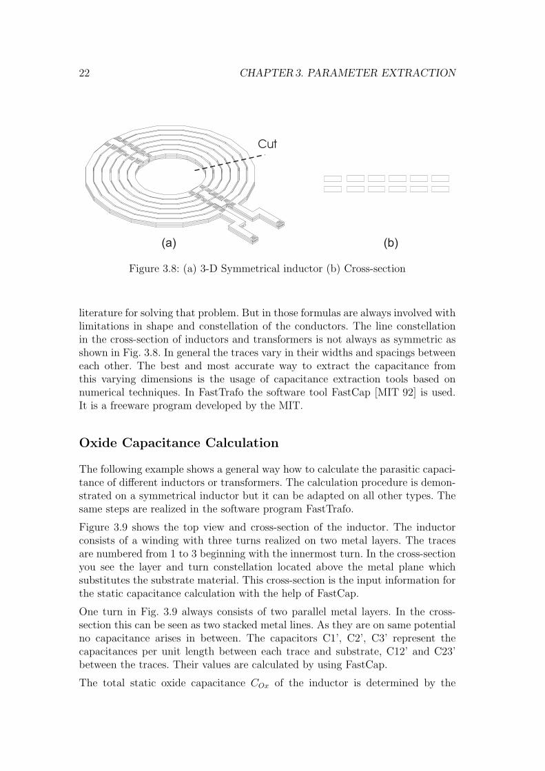
Cut
(a) (b)
Figure 3.8: (a) 3-D Symmetrical inductor (b) Cross-section
literature for solving that problem. But in those formulas are always involved withlimitations in shape and constellation of the conductors. The line constellationin the cross-section of inductors and transformers is not always as symmetric asshown in Fig. 3.8. In general the traces vary in their widths and spacings betweeneach other. The best and most accurate way to extract the capacitance fromthis varying dimensions is the usage of capacitance extraction tools based onnumerical techniques. In FastTrafo the software tool FastCap [MIT 92] is used.It is a freeware program developed by the MIT.
Oxide Capacitance Calculation
The following example shows a general way how to calculate the parasitic capaci-tance of different inductors or transformers. The calculation procedure is demon-strated on a symmetrical inductor but it can be adapted on all other types. Thesame steps are realized in the software program FastTrafo.
Figure 3.9 shows the top view and cross-section of the inductor. The inductorconsists of a winding with three turns realized on two metal layers. The tracesare numbered from 1 to 3 beginning with the innermost turn. In the cross-sectionyou see the layer and turn constellation located above the metal plane whichsubstitutes the substrate material. This cross-section is the input information forthe static capacitance calculation with the help of FastCap.
One turn in Fig. 3.9 always consists of two parallel metal layers. In the cross-section this can be seen as two stacked metal lines. As they are on same potentialno capacitance arises in between. The capacitors C1’, C2’, C3’ represent thecapacitances per unit length between each trace and substrate, C12’ and C23’between the traces. Their values are calculated by using FastCap.
The total static oxide capacitance COx of the inductor is determined by the
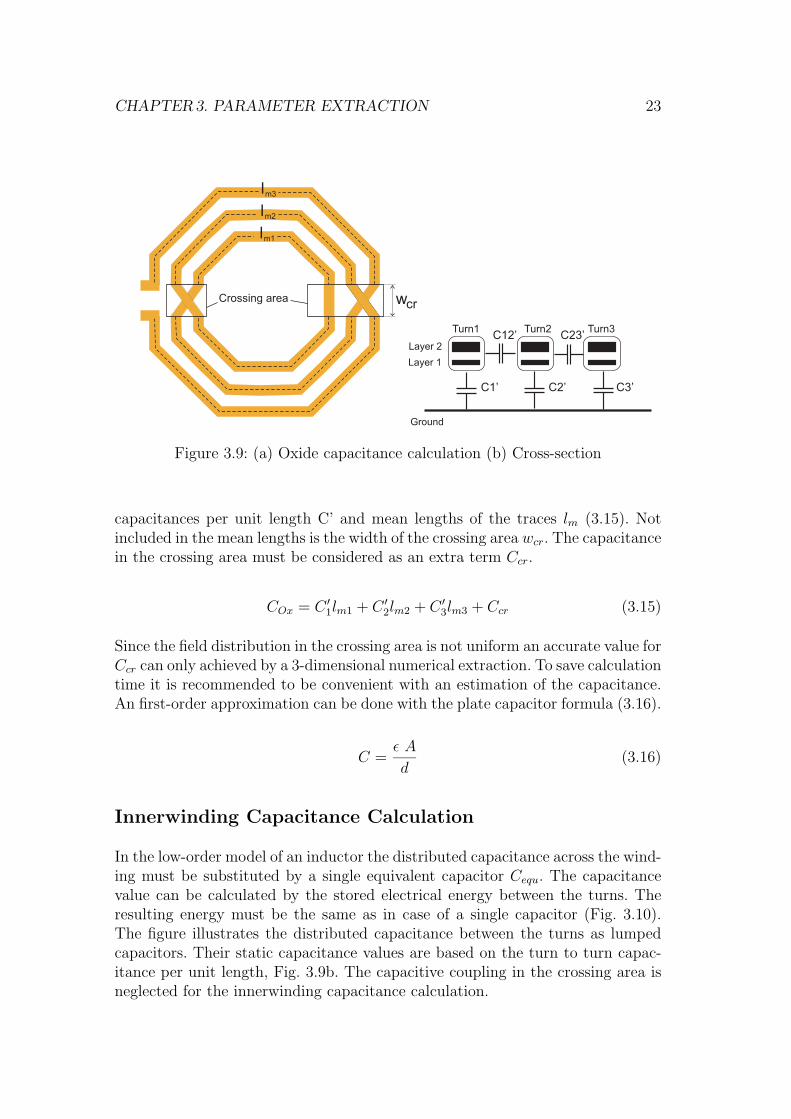
CHAPTER 3. PARAMETER EXTRACTION 23
Turn1 Turn2 Turn3
Crossing area
Figure 3.9: (a) Oxide capacitance calculation (b) Cross-section
capacitances per unit length C’ and mean lengths of the traces lm (3.15). Notincluded in the mean lengths is the width of the crossing area wcr. The capacitancein the crossing area must be considered as an extra term Ccr.
COx = C ′1lm1 + C ′
2lm2 + C ′3lm3 + Ccr (3.15)
Since the field distribution in the crossing area is not uniform an accurate value forCcr can only achieved by a 3-dimensional numerical extraction. To save calculationtime it is recommended to be convenient with an estimation of the capacitance.An first-order approximation can be done with the plate capacitor formula (3.16).
C =ε A
d(3.16)
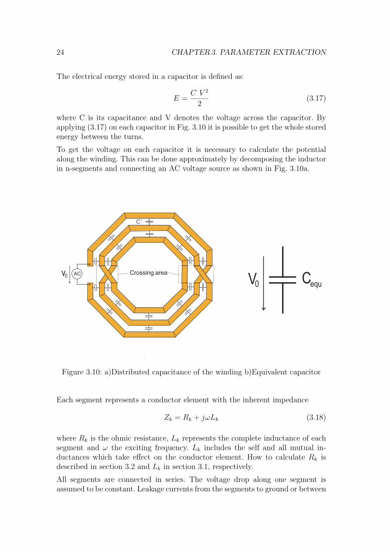
Innerwinding Capacitance Calculation
In the low-order model of an inductor the distributed capacitance across the wind-ing must be substituted by a single equivalent capacitor Cequ. The capacitancevalue can be calculated by the stored electrical energy between the turns. Theresulting energy must be the same as in case of a single capacitor (Fig. 3.10).The figure illustrates the distributed capacitance between the turns as lumpedcapacitors. Their static capacitance values are based on the turn to turn capac-itance per unit length, Fig. 3.9b. The capacitive coupling in the crossing area isneglected for the innerwinding capacitance calculation.
24 CHAPTER 3. PARAMETER EXTRACTION
The electrical energy stored in a capacitor is defined as:
E =C V 2
2(3.17)
where C is its capacitance and V denotes the voltage across the capacitor. Byapplying (3.17) on each capacitor in Fig. 3.10 it is possible to get the whole storedenergy between the turns.
To get the voltage on each capacitor it is necessary to calculate the potentialalong the winding. This can be done approximately by decomposing the inductorin n-segments and connecting an AC voltage source as shown in Fig. 3.10a.
Crossing area
C’
ACv0 V Cequ0
Figure 3.10: a)Distributed capacitance of the winding b)Equivalent capacitor
Each segment represents a conductor element with the inherent impedance
Zk = Rk + jωLk (3.18)
where Rk is the ohmic resistance, Lk represents the complete inductance of eachsegment and ω the exciting frequency. Lk includes the self and all mutual in-ductances which take effect on the conductor element. How to calculate Rk isdescribed in section 3.2 and Lk in section 3.1, respectively.
All segments are connected in series. The voltage drop along one segment isassumed to be constant. Leakage currents from the segments to ground or between
CHAPTER 3. PARAMETER EXTRACTION 25
adjacent segments are neglected. For this reason all segments are flown throughby the same current and the voltage drop on each segment Vk is proportional totheir impedances Zk. From the Kirchoff law it follows that the summation overall n segments voltages leads to the source voltage V0.
Vk ∝ Zk V0 =n∑
k=1
Vk (3.19)
With this two relations the voltage profile across the winding is well defined andthe voltage on each capacitor results as potential difference between two adjacentsegments where it is connected.
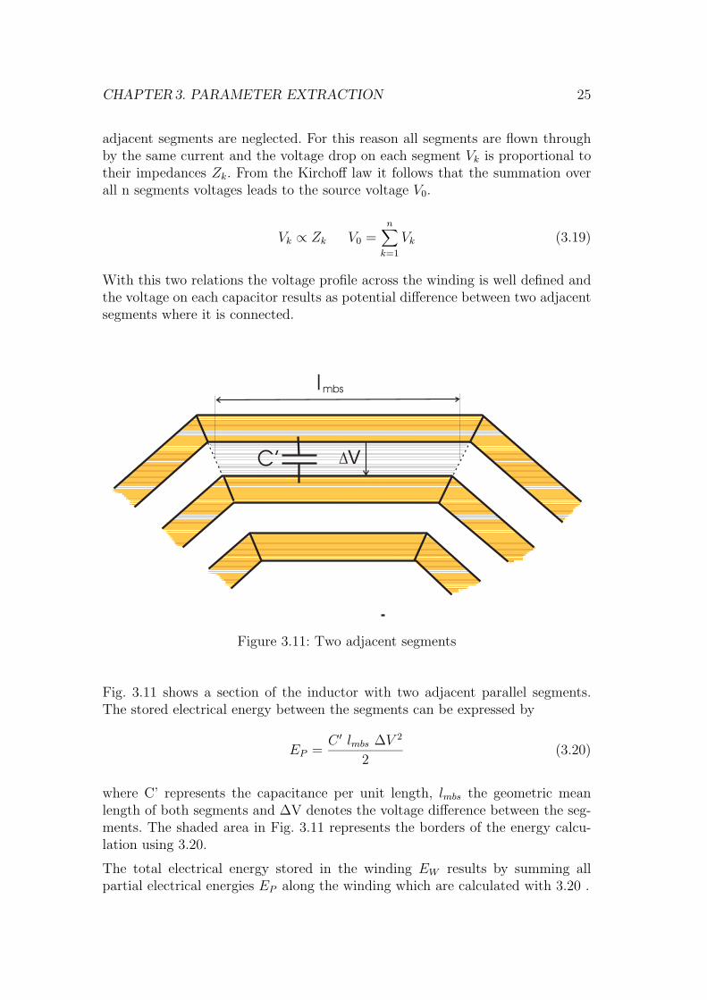
Figure 3.11: Two adjacent segments
Fig. 3.11 shows a section of the inductor with two adjacent parallel segments.The stored electrical energy between the segments can be expressed by
EP =C ′ lmbs ∆V 2
2(3.20)
where C’ represents the capacitance per unit length, lmbs the geometric meanlength of both segments and ∆V denotes the voltage difference between the seg-ments. The shaded area in Fig. 3.11 represents the borders of the energy calcu-lation using 3.20.
The total electrical energy stored in the winding EW results by summing allpartial electrical energies EP along the winding which are calculated with 3.20 .
26 CHAPTER 3. PARAMETER EXTRACTION
EW =∑k
EP,k (3.21)
The equivalent capacitor must store the same electric energy EW as the winding.From (3.22), (3.20) and (3.17) follow the capacitance value for the equivalentcapacitor Cequ
Cequ =1
V 20
∑k
C ′ lmbs,k ∆V 2k (3.22)
V0 represents the applied voltage between the two winding ports, C’ representsthe capacitance per unit length between the turns. lmbs,k is the mean lengthbetween two adjacent parallel segments and Vk the potential difference betweenthese segments (Fig. 3.11).
CHAPTER 3. PARAMETER EXTRACTION 27
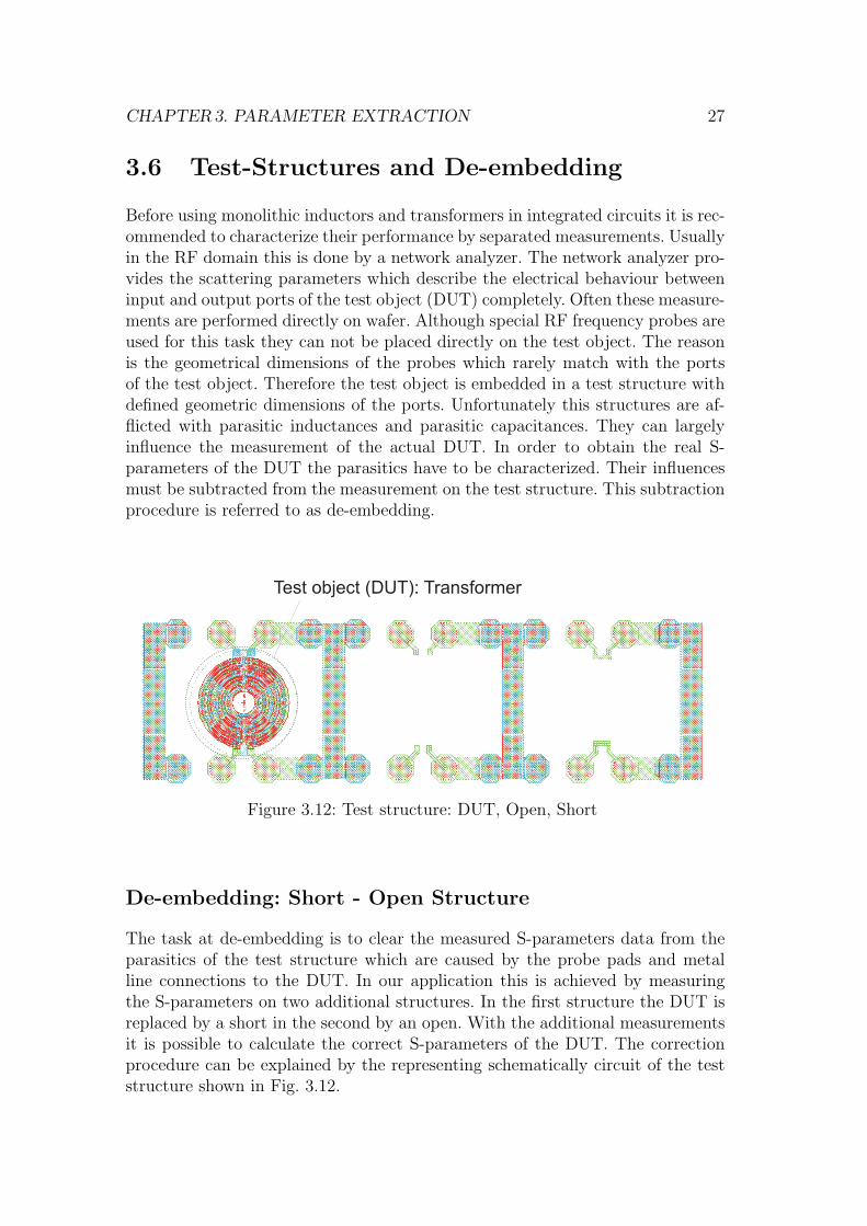
3.6 Test-Structures and De-embedding
Before using monolithic inductors and transformers in integrated circuits it is rec-ommended to characterize their performance by separated measurements. Usuallyin the RF domain this is done by a network analyzer. The network analyzer pro-vides the scattering parameters which describe the electrical behaviour betweeninput and output ports of the test object (DUT) completely. Often these measure-ments are performed directly on wafer. Although special RF frequency probes areused for this task they can not be placed directly on the test object. The reasonis the geometrical dimensions of the probes which rarely match with the portsof the test object. Therefore the test object is embedded in a test structure withdefined geometric dimensions of the ports. Unfortunately this structures are af-flicted with parasitic inductances and parasitic capacitances. They can largelyinfluence the measurement of the actual DUT. In order to obtain the real S-parameters of the DUT the parasitics have to be characterized. Their influencesmust be subtracted from the measurement on the test structure. This subtractionprocedure is referred to as de-embedding.
Test object (DUT): Transformer
Figure 3.12: Test structure: DUT, Open, Short
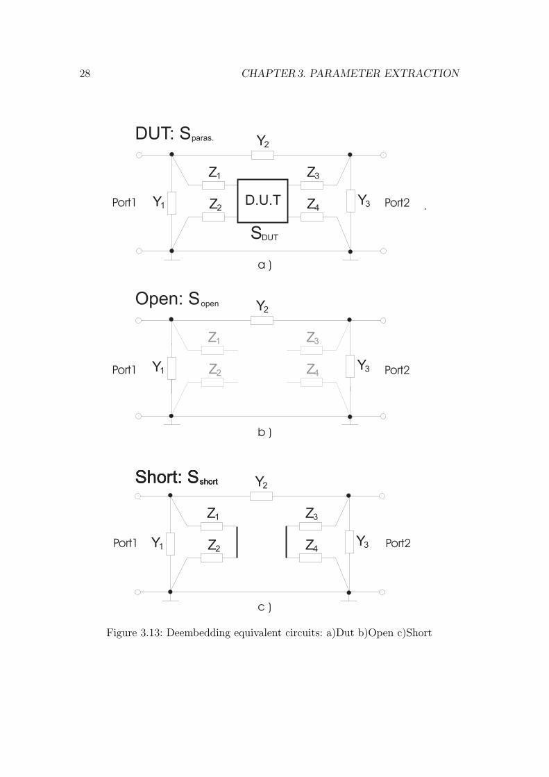
De-embedding: Short - Open Structure
The task at de-embedding is to clear the measured S-parameters data from theparasitics of the test structure which are caused by the probe pads and metalline connections to the DUT. In our application this is achieved by measuringthe S-parameters on two additional structures. In the first structure the DUT isreplaced by a short in the second by an open. With the additional measurementsit is possible to calculate the correct S-parameters of the DUT. The correctionprocedure can be explained by the representing schematically circuit of the teststructure shown in Fig. 3.12.
28 CHAPTER 3. PARAMETER EXTRACTION
D.U.TY1
Z1 Z3
Z4Z2
Y2
Y3Port1 .
Y1
Z1 Z3
Z4Z2
Y2
Y3
Y1
Z1 Z3
Z4Z2
Y2
Y3
Open: S
Short: S
DUT: Sparas.
short
open
Short: SshortShort: Sshort
DUTS
Port1
Port1
Port2
Port2
Port2
a )
b )
c )
Figure 3.13: Deembedding equivalent circuits: a)Dut b)Open c)Short
CHAPTER 3. PARAMETER EXTRACTION 29
Figure 3.13a shows a suitable equivalent circuit diagram of the test structurewith DUT. On the left and right side are the ports where the probes are placedduring the measurement. The DUT is symbolized by a two port box. The box issurrounded by admittances and impedances which represent the additional par-asitic influences due to the test structure. The admittances Y1, Y3, represent thecapacitive coupling between the metal interconnections and the silicon substrateon each port, Y2 the capacitive coupling between the ports. Z1, Z3, originate fromthe metal interconnections series impedances between the ports on the test struc-ture and the DUT on the other. Z2, Z4 represent the serial metal interconnectionsfrom the DUT to ground.
Figure 3.13b shows the circuit in case of an open. The serial impedances Z1-Z4
are not connected anywhere and are ineffective. Just the admittances Y1, Y2, Y3
remain in the measurement.
Figure 3.13c shows the short de-embedding circuit. Now the impedances Z1, Z2
and Z3, Z4 are connected between signal and ground.
With the three measured S-parameters sets Sparas., Sshort, Sopen (Fig. 3.13) aformula can be specified which leads to the correct S-parameter set SDUT of theDUT. This is proceed with help of the impedance and admittance matrices. Fora conversion of the matrices exists the relations [Zinke 95]:
Y =1
Z0
[(E − S)(E + S)−1
](3.23)
Z = Z0
[(E + S)(E − S)−1
](3.24)
S = (Z/Z0 − E)(Z/Z0 + E)−1 (3.25)
S = (E − Z0Y)(E + Z0Y)−1 (3.26)
Z = Y−1 (3.27)
where Z0 is the characteristic impedance of the measurement system and E rep-resents the identity matrix with ones on the diagonal and zeros elsewhere.
E =
(1 00 1
)
As shown in figure 3.13b the parasitic admittances Y1-Y3 can be easily found bythe open configuration. For determination of the parasitic impedances Z1-Z4 itis necessary to consider the open and short configuration. The impedance matrixwith the parasitic impedances Z1-Z4 yields from the subtraction of open and shortadmittance matrices (3.28).
ZparsiticZ = (Yshort − Yopen)−1 (3.28)
Now, the correct Z-parameter of the DUT can be attained by subtracting ZparsiticZ .

30 CHAPTER 3. PARAMETER EXTRACTION
ZDUT = (Yparas. − Yopen)−1 − ZparsiticZ (3.29)
Applying (3.25) yields the correct S-parameter of the DUT
Chapter 4
Experimental Results
In this chapter measurement results are compared to FastTrafo simulation results.This is done by an example of an inductor and a transformer in silicon bipolartechnology. Further in the first example the increasing accuracy in prediction byusing a second order model will be illustrated in comparison to the first ordermodel.
The measurements on the transformer and inductor were done with a two portnetwork analyzer in a Z0 = 50 Ω test system. The used test structure and de-embedding procedure are introduced in section 3.6. The network analyzer providesthe scattering parameters of the test object. With the help of the transformationformulas 3.23 - 3.27 other relevant parameters of the test object can be derived.Such parameters are introduced in this chapter.
4.1 A 4.7nH Inductor for 2 GHz
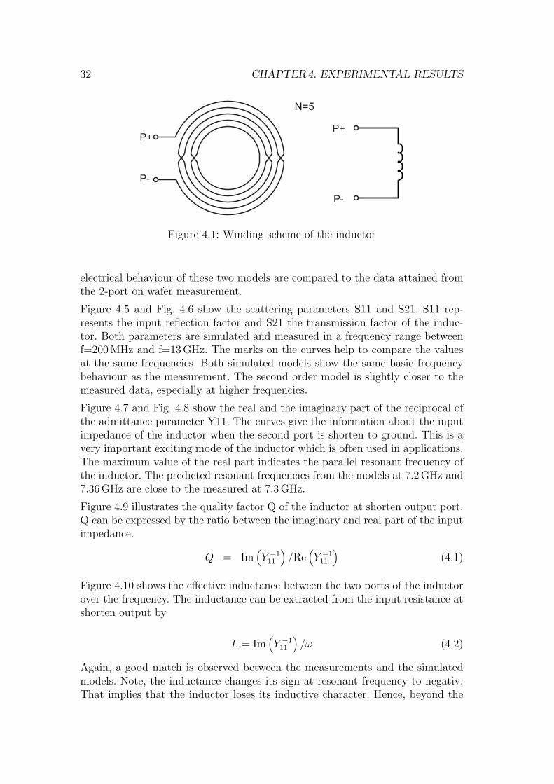
The introduced inductor in this section consists of a symmetrical winding withN=5 turns (Fig. 4.1). The inductance is about 4.7 nH at low frequencies. The selfresonant frequency of the inductor is near 7.3 GHz.
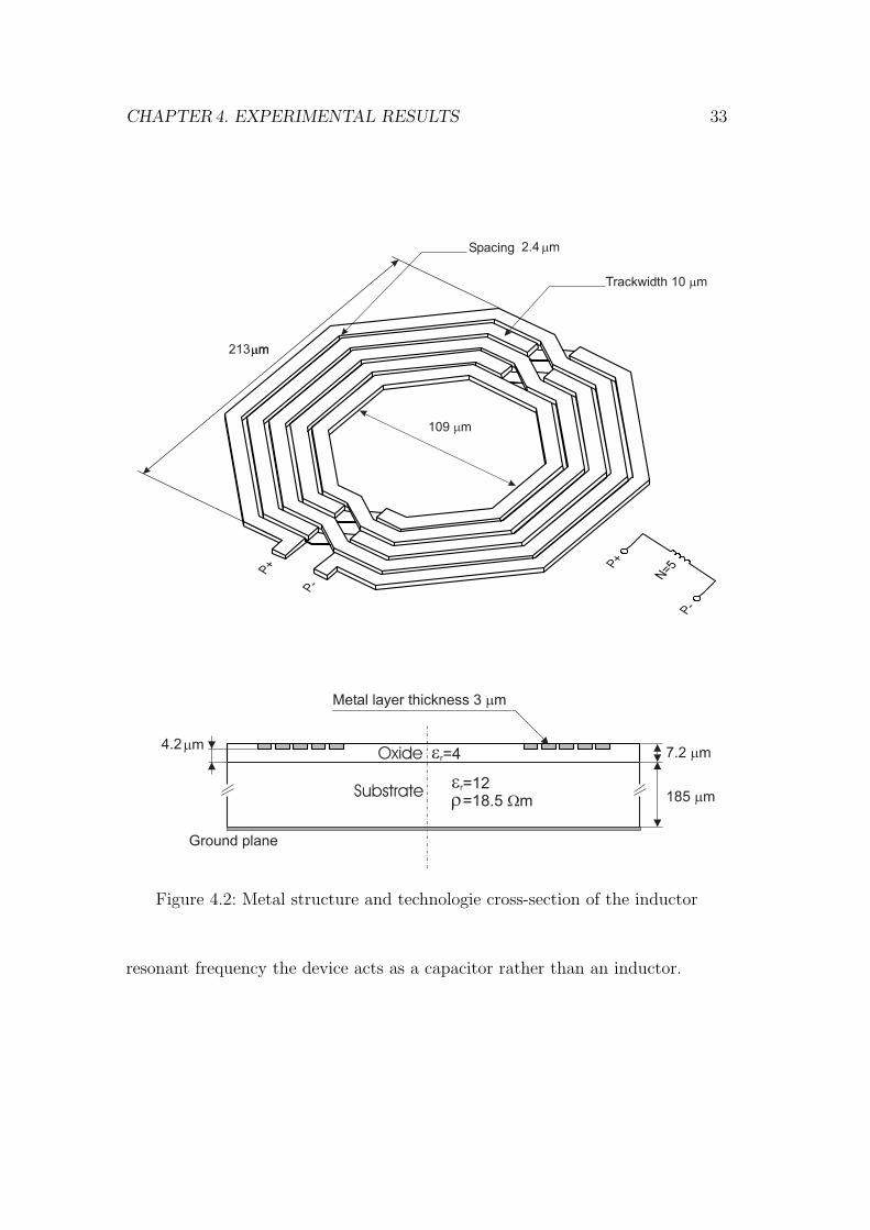
The inductor is fabricated in the Si bipolar process B7HF. In this process themetal layers consist of aluminium (σ = 33e6 S/m) and are embedded in silicon-dioxide SiO2, which has a relative permittivity of εr=3.9. The oxide is arrangedover a p−- doped silicon substrate, which has a εr=11.9 and a conductance of5.4 S/m. Although the process allows several metal layers, the winding residesjust on one single metal layer. An additional second metal layer is only used forthe interconnection between the turns. Fig.4.2 illustrates the metal structure ofthe winding and a cross section from the technology.
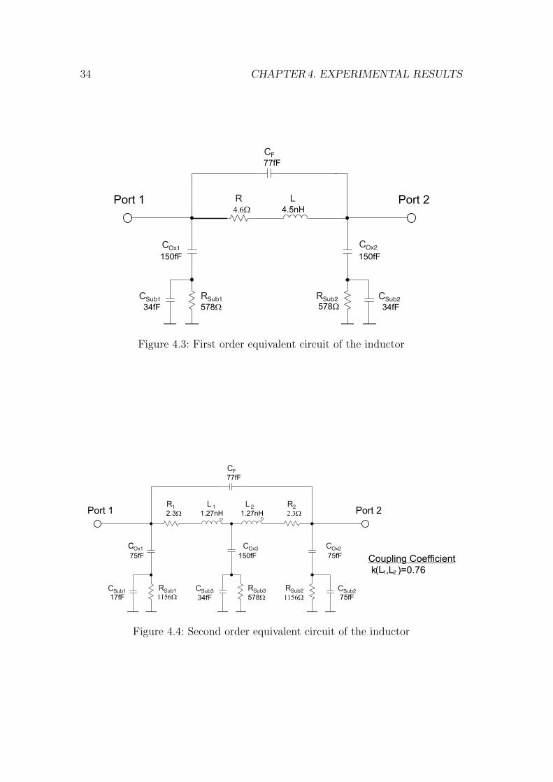
With the given dimensions of the winding and the technology data FastTrafoprovides a first order electrical model (Fig. 4.3) and a second order electricalmodel (Fig. ??) of the inductor after parameter extraction. In the following the
31
32 CHAPTER 4. EXPERIMENTAL RESULTS
Figure 4.1: Winding scheme of the inductor
electrical behaviour of these two models are compared to the data attained fromthe 2-port on wafer measurement.
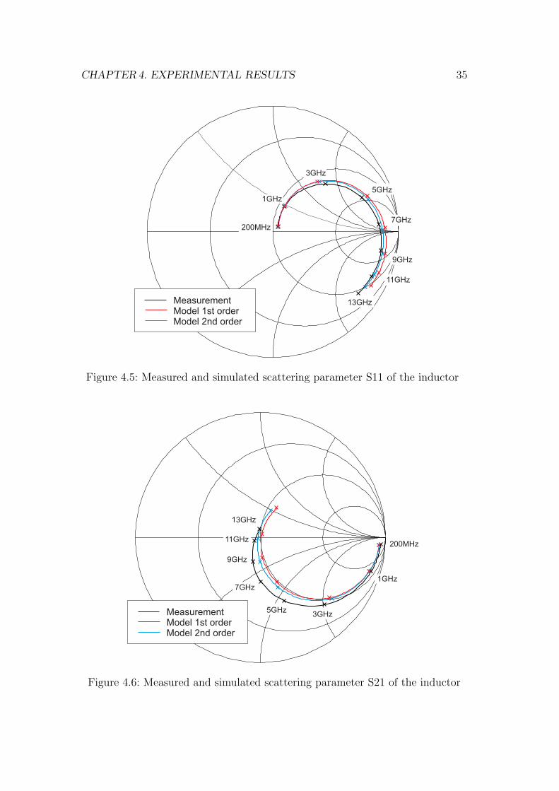
Figure 4.5 and Fig. 4.6 show the scattering parameters S11 and S21. S11 rep-resents the input reflection factor and S21 the transmission factor of the induc-tor. Both parameters are simulated and measured in a frequency range betweenf=200 MHz and f=13 GHz. The marks on the curves help to compare the valuesat the same frequencies. Both simulated models show the same basic frequencybehaviour as the measurement. The second order model is slightly closer to themeasured data, especially at higher frequencies.
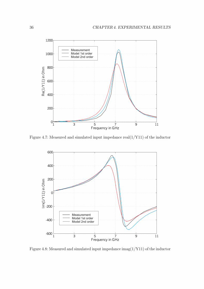
Figure 4.7 and Fig. 4.8 show the real and the imaginary part of the reciprocal ofthe admittance parameter Y11. The curves give the information about the inputimpedance of the inductor when the second port is shorten to ground. This is avery important exciting mode of the inductor which is often used in applications.The maximum value of the real part indicates the parallel resonant frequency ofthe inductor. The predicted resonant frequencies from the models at 7.2 GHz and7.36 GHz are close to the measured at 7.3 GHz.
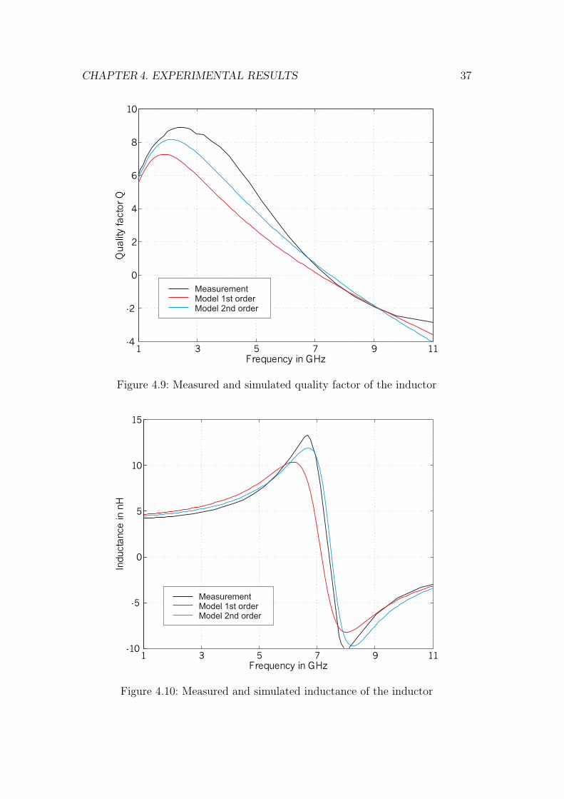
Figure 4.9 illustrates the quality factor Q of the inductor at shorten output port.Q can be expressed by the ratio between the imaginary and real part of the inputimpedance.
Q = Im(Y −1
11
)/Re
(Y −1
11
)(4.1)
Figure 4.10 shows the effective inductance between the two ports of the inductorover the frequency. The inductance can be extracted from the input resistance atshorten output by
L = Im(Y −1
11
)/ω (4.2)
Again, a good match is observed between the measurements and the simulatedmodels. Note, the inductance changes its sign at resonant frequency to negativ.That implies that the inductor loses its inductive character. Hence, beyond the
CHAPTER 4. EXPERIMENTAL RESULTS 33
Figure 4.2: Metal structure and technologie cross-section of the inductor
resonant frequency the device acts as a capacitor rather than an inductor.
34 CHAPTER 4. EXPERIMENTAL RESULTS
Figure 4.3: First order equivalent circuit of the inductor
Figure 4.4: Second order equivalent circuit of the inductor
CHAPTER 4. EXPERIMENTAL RESULTS 35
Figure 4.5: Measured and simulated scattering parameter S11 of the inductor
Figure 4.6: Measured and simulated scattering parameter S21 of the inductor
36 CHAPTER 4. EXPERIMENTAL RESULTS
Figure 4.7: Measured and simulated input impedance real(1/Y11) of the inductor
Figure 4.8: Measured and simulated input impedance imag(1/Y11) of the inductor
CHAPTER 4. EXPERIMENTAL RESULTS 37
Figure 4.9: Measured and simulated quality factor of the inductor
Figure 4.10: Measured and simulated inductance of the inductor
38 CHAPTER 4. EXPERIMENTAL RESULTS
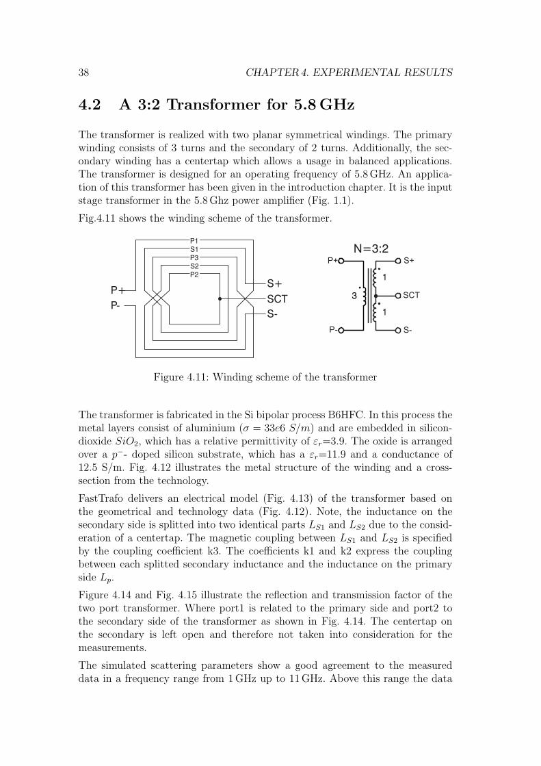
4.2 A 3:2 Transformer for 5.8 GHz
The transformer is realized with two planar symmetrical windings. The primarywinding consists of 3 turns and the secondary of 2 turns. Additionally, the sec-ondary winding has a centertap which allows a usage in balanced applications.The transformer is designed for an operating frequency of 5.8 GHz. An applica-tion of this transformer has been given in the introduction chapter. It is the inputstage transformer in the 5.8 Ghz power amplifier (Fig. 1.1).
Fig.4.11 shows the winding scheme of the transformer.
P+
P-
S+
S-
P1
S1
P3
S2
P2
P-
P+
3 SCT
S-
1
S+
1
N=3:2
SCT
Figure 4.11: Winding scheme of the transformer
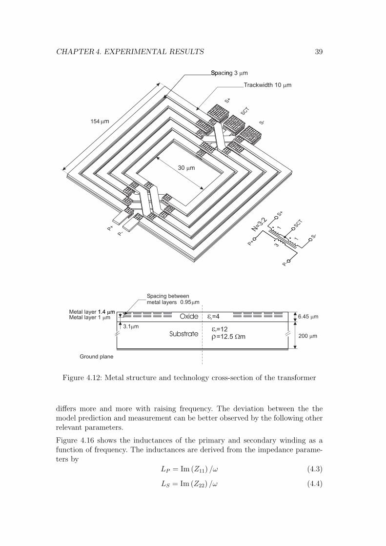
The transformer is fabricated in the Si bipolar process B6HFC. In this process themetal layers consist of aluminium (σ = 33e6 S/m) and are embedded in silicon-dioxide SiO2, which has a relative permittivity of εr=3.9. The oxide is arrangedover a p−- doped silicon substrate, which has a εr=11.9 and a conductance of12.5 S/m. Fig. 4.12 illustrates the metal structure of the winding and a cross-section from the technology.
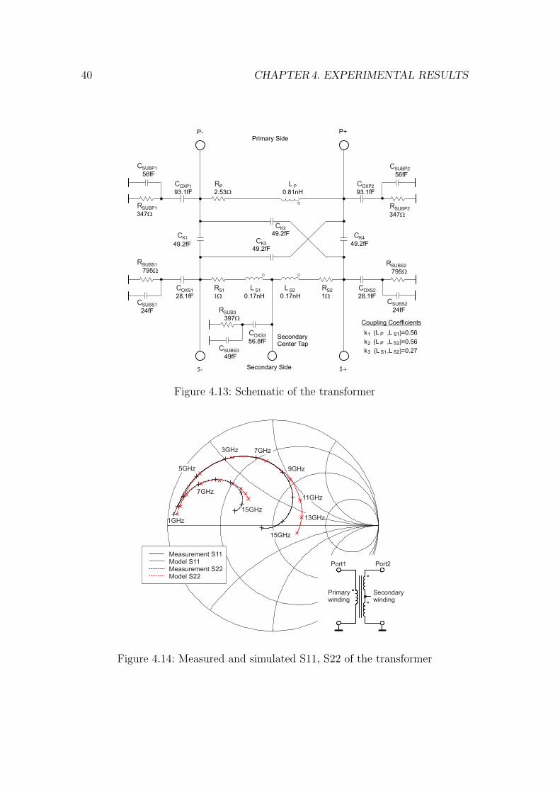
FastTrafo delivers an electrical model (Fig. 4.13) of the transformer based onthe geometrical and technology data (Fig. 4.12). Note, the inductance on thesecondary side is splitted into two identical parts LS1 and LS2 due to the consid-eration of a centertap. The magnetic coupling between LS1 and LS2 is specifiedby the coupling coefficient k3. The coefficients k1 and k2 express the couplingbetween each splitted secondary inductance and the inductance on the primaryside Lp.
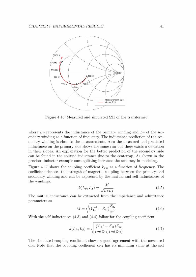
Figure 4.14 and Fig. 4.15 illustrate the reflection and transmission factor of thetwo port transformer. Where port1 is related to the primary side and port2 tothe secondary side of the transformer as shown in Fig. 4.14. The centertap onthe secondary is left open and therefore not taken into consideration for themeasurements.
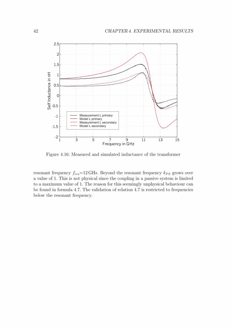
The simulated scattering parameters show a good agreement to the measureddata in a frequency range from 1 GHz up to 11 GHz. Above this range the data
CHAPTER 4. EXPERIMENTAL RESULTS 39
Figure 4.12: Metal structure and technology cross-section of the transformer
differs more and more with raising frequency. The deviation between the themodel prediction and measurement can be better observed by the following otherrelevant parameters.
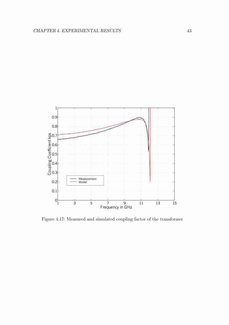
Figure 4.16 shows the inductances of the primary and secondary winding as afunction of frequency. The inductances are derived from the impedance parame-ters by
LP = Im (Z11) /ω (4.3)
LS = Im (Z22) /ω (4.4)
40 CHAPTER 4. EXPERIMENTAL RESULTS
Figure 4.13: Schematic of the transformer
Figure 4.14: Measured and simulated S11, S22 of the transformer
CHAPTER 4. EXPERIMENTAL RESULTS 41
Figure 4.15: Measured and simulated S21 of the transformer
where LP represents the inductance of the primary winding and LS of the sec-ondary winding as a function of frequency. The inductance prediction of the sec-ondary winding is close to the measurements. Also the measured and predictedinductance on the primary side shows the same run but there exists a deviationin their slopes. An explanation for the better prediction of the secondary sidecan be found in the splitted inductance due to the centertap. As shown in theprevious inductor example such splitting increases the accuracy in modeling.
Figure 4.17 shows the coupling coefficient kPS as a function of frequency. Thecoefficient denotes the strength of magnetic coupling between the primary andsecondary winding and can be expressed by the mutual and self inductances ofthe windings.
k(LP , LS) =M√LP LS
(4.5)
The mutual inductance can be extracted from the impedance and admittanceparameters as
M =
√(Y −1
11 − Z11)Z22
ω2(4.6)
With the self inductances (4.3) and (4.4) follow for the coupling coefficient
k(LP , LS) =
√√√√ (Y −111 − Z11)Z22
Im(Z11)Im(Z22)(4.7)
The simulated coupling coefficient shows a good agreement with the measuredone. Note that the coupling coefficient kPS has its minimum value at the self
42 CHAPTER 4. EXPERIMENTAL RESULTS
Measurement L primaryModel L primaryMeasurement L secondaryModel L secondary
Figure 4.16: Measured and simulated inductance of the transformer
resonant frequency fres=12 GHz. Beyond the resonant frequency kPS grows overa value of 1. This is not physical since the coupling in a passive system is limitedto a maximum value of 1. The reason for this seemingly unphysical behaviour canbe found in formula 4.7. The validation of relation 4.7 is restricted to frequenciesbelow the resonant frequency.
CHAPTER 4. EXPERIMENTAL RESULTS 43
MeasurementModel
Figure 4.17: Measured and simulated coupling factor of the transformer

44 CHAPTER 4. EXPERIMENTAL RESULTS
Chapter 5
Conclusion
In this work methods have been presented that allow a fast characterization ofmonolithic integrated inductors and transformers in Si/SiGe bipolar and CMOStechnologies. The characterization is based on an equivalent electrical low-ordermodel. All parameters of the model are extracted from the physical structure ofthe device.
A user-friendly program FastTrafo v3.2 has been developed which incorporates allmethods discussed in this thesis. The short computation time and easy handlingof the program allows the chip designer to find out the optimum inductors andtransformers for different integrated circuit designs.
The models provided by FastTrafo v3.2 have been verified by measurements onseveral inductors and transformers. The devices have varied in their geometriesand operating frequencies. The models and measurements show a good agree-ment up to their self resonant frequency. The verification was performed up to afrequency of 25 GHz. Two design examples are presented in this work.
The program is used in different divisions of Infineon Technologies. For instance,it is used in the divisions Wireless Solution and Automotive&Industrial for de-signing and optimizing transformers for integrated power amplifier and integratedhigh voltage applications, respectively.
45

46 CHAPTER 5. CONCLUSION
Appendix A
FastTrafo User Manual
Introduction
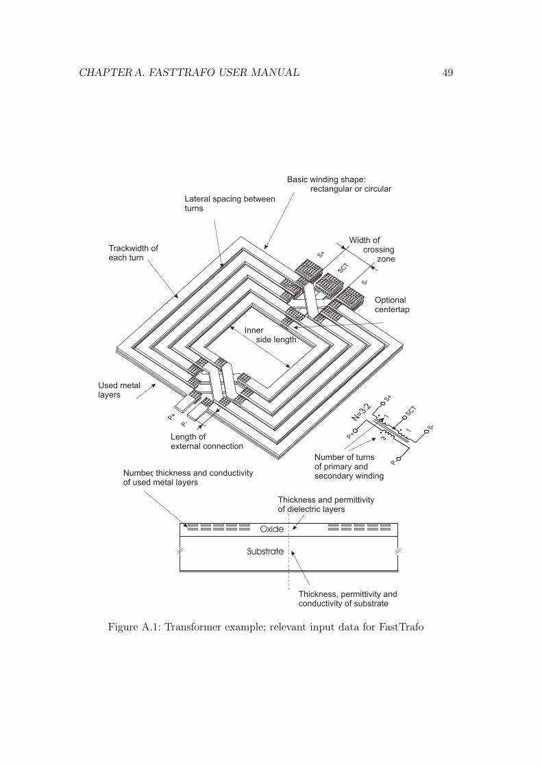
This manual describes FastTrafo, a parameter extraction program for monolithicintegrated lumped transformers and inductors. FastTrafo computes self and mu-tual inductance, resistance and capacitance between primary winding, secondarywinding and substrate. After calculation FastTrafo provides a compact electricalSPICE model and a characterization of the transformer will be displayed on thescreen.
FastTrafo is able to handle different transformer and inductor structures. The userof FastTrafo has to specify the physical dimensions of the device and electricalproperties of the used materials. Fig. A.1 shows an example of a planar rectan-gular transformer. It illustrates the relevant input data for a characterization ofthe device with FastTrafo.
The characterization of the devices is based on electrical lumped low order models.The parameters of the models are extracted from the geometrical structure of theinductor or transformer by using FEM-Tools (Finite Element Method) and ana-lytical considerations. The capacitance and inductance calculation are reduced toelectrostatic and quasimagnetostatic calculations. Therefore, compared with fullmaxwell field solvers the computing time is very short. The used FEM-Tools inthe program core of FastTrafo are called FastHenry and FastCap. FastHenry isa three dimensional extraction algorithm for inductance calculation and FastCapfor capacitance calculation, respectively. Both are developed by the MIT (Mes-sachusetts Institude of Technology). For detailed information about the internalalgorithms take a look in their manuals [MIT 96], [MIT 92]. Information aboutthe application of FastHenry and FastCap in the program core of FastTrafo canbe found in chapter 3 of this thesis. Also in chapter 3 the calculation of thesubstrate resistance is explained.
Note: In the actual program version FastTrafo v3.2 a full characteri-zation is only possible for transformers. The inductor and autotrans-
47
48 CHAPTER A. FASTTRAFO USER MANUAL
former calculation is limited to inductance extraction and couplingcoefficients, respectively.
The manual is divided into four sections. The first section explains the handlingof the graphical interface. The interface creates an input file for FastTrafo whichcontains the description of the transformer geometries. The second section showshow to create a technology file. The technology file contains all necessary infor-mation of the semiconductor process. The third sections subject are the outputsof FastTrafo. The fourth section lists the system requirements to run FastTrafo.
FastTrafo Install
FastTrafo v3 2 install.exe is a self-extracting archive. It contains all the filesneeded to run FastTrafo on your windows system. The file is compressed withthe standard WinZip program. Double-click on this self-extracting archive file tounpack its contents on the specified path. A new directory FTrafo v3 2 shouldbe automatically generated on the entered path. Make Ftrafo v3 2 to the currentdirectory and click ftraforun.exe to start the program. A graphical user-windowand a DOS window should appear on the screen.
CHAPTER A. FASTTRAFO USER MANUAL 49
Figure A.1: Transformer example; relevant input data for FastTrafo
50 CHAPTER A. FASTTRAFO USER MANUAL
How to Prepare an Input File
The Graphical Interface
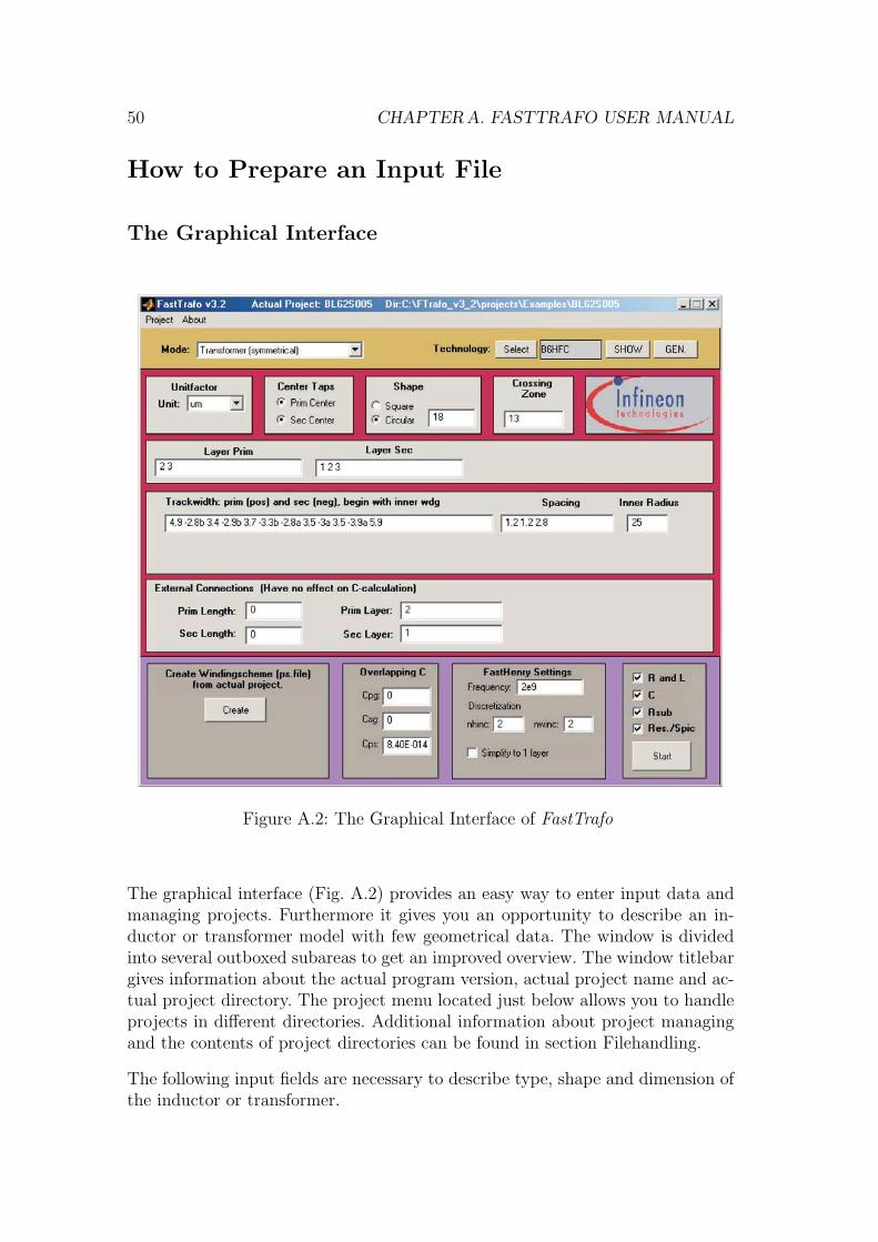
Figure A.2: The Graphical Interface of FastTrafo
The graphical interface (Fig. A.2) provides an easy way to enter input data andmanaging projects. Furthermore it gives you an opportunity to describe an in-ductor or transformer model with few geometrical data. The window is dividedinto several outboxed subareas to get an improved overview. The window titlebargives information about the actual program version, actual project name and ac-tual project directory. The project menu located just below allows you to handleprojects in different directories. Additional information about project managingand the contents of project directories can be found in section Filehandling.
The following input fields are necessary to describe type, shape and dimension ofthe inductor or transformer.

CHAPTER A. FASTTRAFO USER MANUAL 51
The Geometry Inputs
• ModeThis pop-up menu defines the type of transformer and inductor that willbe treated. You have the choice between six different types:
Transformers (symmetrical)Transformers (stacked, symmetrical)Transformers (stacked, spiral)Autotransformers = Coils with centertapsCoils (spiral)Coils (symmetrical)
Note, after selection some input fields would be de- or activated becausethe types require different sets of various geometric input fields. Examplesof the different options are shown in section Design Examples.
• TechnologyThe Select-button gives a list of all available technology-files.The Show-button displays a description of the actual technology-file.The Gen-button allows to generate new technology files.How to write such a technology-file is explained in section Technology-file.
• UnitSpecifies the used length unit.Available options are: um(=µm) mm cm m
• Center TapsIn case of transformer calculations you have the option to place centertapson the primary and/or the secondary winding. The centertap will be placeddirectly on the winding. No external line connections to the centertap aretaken into account.
• ShapeYou can select rectangular or circular shapes for your designs. If you activatethe circular shape option you have also to enter a numerical value in thewhite field. This value specifies the number of sides of a polygon whichapproximate the circle. Note that the number must be an even number. Auseful range is from 6 up to 20.
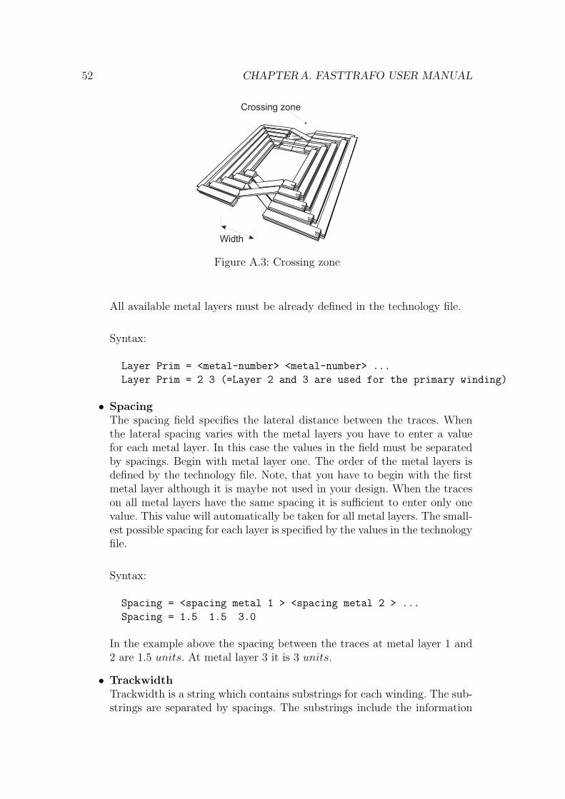
• Crossing ZoneIn this manual the area where the traces from different turns cross each otheris called crossing zone. The value denotes the width of the zone (Fig. A.3).Note: The width can not be larger than the double inner radius.
• Metal LayersLayer Prim and Layer Sec specify the parallel connected metal layersthat are used for the realization of the primary and secondary winding. En-ter the used metal layers as numbers. They must be separated by spacings.
52 CHAPTER A. FASTTRAFO USER MANUAL
Crossing zone
Width
Figure A.3: Crossing zone
All available metal layers must be already defined in the technology file.
Syntax:
Layer Prim = <metal-number> <metal-number> ...
Layer Prim = 2 3 (=Layer 2 and 3 are used for the primary winding)
• SpacingThe spacing field specifies the lateral distance between the traces. Whenthe lateral spacing varies with the metal layers you have to enter a valuefor each metal layer. In this case the values in the field must be separatedby spacings. Begin with metal layer one. The order of the metal layers isdefined by the technology file. Note, that you have to begin with the firstmetal layer although it is maybe not used in your design. When the traceson all metal layers have the same spacing it is sufficient to enter only onevalue. This value will automatically be taken for all metal layers. The small-est possible spacing for each layer is specified by the values in the technologyfile.
Syntax:
Spacing = <spacing metal 1 > <spacing metal 2 > ...
Spacing = 1.5 1.5 3.0
In the example above the spacing between the traces at metal layer 1 and2 are 1.5 units. At metal layer 3 it is 3 units.
• TrackwidthTrackwidth is a string which contains substrings for each winding. The sub-strings are separated by spacings. The substrings include the information
CHAPTER A. FASTTRAFO USER MANUAL 53
about the trackwidth and the parallel connections of primary and secondaryturns. The string begins with the substring of the innermost turn and endswith the outermost turn of the transformer or inductor. The values givenfor the trackwidthes are valid for the last metal layer (highest number intechnology file) used in the transformer design. The trackwidthes for theused layers below are automatically generated considering their spacing val-ues.
Syntax:
Trackwidth = <+/-><width><group> <+/-><width><group> ...
Trackwidth = 5.9 -3.9a 3 -3.5a
Each substring starts with a float number. The numbers define the track-widthes of the turns. A positive number means the turn belongs to the pri-mary winding and a negative number to secondary winding, respectively.Letters can be attached to the numbers. The letters allow you to set severalturns parallel within one winding. All turns with the same letter or stringare connected in parallel.In the given example the transformer has four turns. The innermost turnbelongs to the primary winding with a trackwidth of 5.9 units followedby a secondary winding turn with a trackwidth of 3.9 units. The secondand the fourth turn have the same group string and therefore they are con-nected in parallel. Between the two secondary winding turns is a primaryturn with 3.0 units trackwidth. Hence, the example-transformer above hasa turn ratio of 2 : 1.
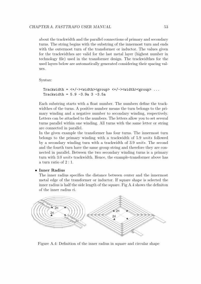
• Inner RadiusThe inner radius specifies the distance between center and the innermostmetal edge of the transformer or inductor. If square shape is selected theinner radius is half the side length of the square. Fig A.4 shows the definitonof the inner radius ri.
2ri2ri
2ri
2ri
Figure A.4: Definition of the inner radius in square and circular shape
54 CHAPTER A. FASTTRAFO USER MANUAL
• External ConnectionsWith these fields you have the option to specify lengths and layers of ex-ternal line connections. The reference point is the outermost metal edgeof the transformer or inductor. The widths of the external connections aregenerated automatically as wide as the trackwidth of the outermost turnwhere they are connected. If the length field contains an empty string or 0no external connections will be taken into account.
The Simulation Inputs
• FrequencyThis field specifies the frequency of interest. Usually it is the operatingfrequency of the inductor or transformer. The frequency is considered atparameters which are calculated with FastHenry. These parameters are theinductance and the serial resistance.
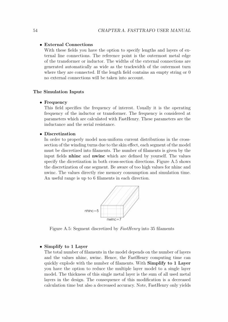
• DiscretizationIn order to properly model non-uniform current distributions in the cross-section of the winding turns due to the skin effect, each segment of the modelmust be discretized into filaments. The number of filaments is given by theinput fields nhinc and nwinc which are defined by yourself. The valuesspecify the dicretization in both cross-section directions. Figure A.5 showsthe discretization of one segment. Be aware of too high values for nhinc andnwinc. The values directly rise memory consumption and simulation time.An useful range is up to 6 filaments in each direction.
nwinc=7
nhinc=5
Figure A.5: Segment discretized by FastHenry into 35 filaments
• Simplify to 1 LayerThe total number of filaments in the model depends on the number of layersand the values nhinc, nwinc. Hence, the FastHenry computing time canquickly explode with the number of filaments. With Simplify to 1 Layeryou have the option to reduce the multiple layer model to a single layermodel. The thickness of this single metal layer is the sum of all used metallayers in the design. The consequence of this modification is a decreasedcalculation time but also a decreased accuracy. Note, FastHenry only yields
CHAPTER A. FASTTRAFO USER MANUAL 55
the serial resistance and inductance. All other parameters will be calculatedin the multiple layer model.
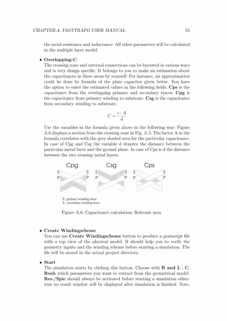
• Overlapping-CThe crossing zone and external connections can be layouted in various waysand is very design specific. It belongs to you to make an estimation aboutthe capacitances in these areas by yourself. For instance, an approximationcould be done by formula of the plate capacitor given below. You havethe option to enter the estimated values in the following fields. Cps is thecapacitance from the overlapping primary and secondary traces. Cpg isthe capacitance from primary winding to substrate. Csg is the capacitancefrom secondary winding to substrate.
C =ε · A
d
Use the variables in the formula given above in the following way: FigureA.6 displays a section from the crossing zone in Fig. A.3. The factor A in theformula correlates with the grey shaded area for the particular capacitance.In case of Cpg and Csg the variable d denotes the distance between theparticular metal layer and the ground plane. In case of Cps is d the distancebetween the two crossing metal layers.
P P
S S
P P
S S
P P
S S
Cpg Csg Cps
P...primary winding traceS...secondary winding trace
Figure A.6: Capacitance calculation: Relevant area
• Create WindingschemeYou can use Create Windingscheme button to produce a postscript filewith a top view of the physical model. It should help you to verify thegeometry inputs and the winding scheme before starting a simulation. Thefile will be stored in the actual project directory.
• StartThe simulation starts by clicking this button. Choose with R and L , C,Rsub which parameters you want to extract from the geometrical model.Res./Spic should always be activated before starting a simulation other-wise no result window will be displayed after simulation is finished. Note,
56 CHAPTER A. FASTTRAFO USER MANUAL
after pressing the Start-button all previous results will be deleted. Excep-tionally, in case of all parameters are deactivated and Res./Spic is activatedthe results window based on previous simulations is shown without deletingany files.
Technology-File
A technology file contains information about the metalization process. This infor-mation involves the distances and properties of the materials. FastTrafo uses thetechnology files combined with the geometric input data to generate the trans-former or inductor model. All user created technology files will be stored in thedirectory .../FTRAFO/TECH and can be reloaded any time.
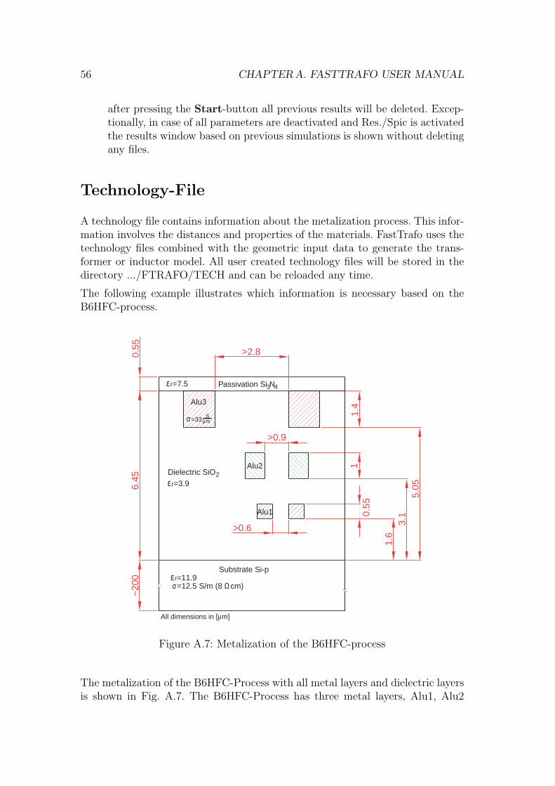
The following example illustrates which information is necessary based on theB6HFC-process.
>2.80.55
6.45
~20
0
1.6
3.1
5.05
10.
551.
4
>0.9
>0.6
Passivation Si Nεr=7.5
εr=3.9
εr=11.9σ=12.5 S/m (8 Ωcm)
Dielectric SiO
Substrate Si-p
σ=33µmS
Alu3
Alu2
Alu1
All dimensions in [µm]
2
3 4
Figure A.7: Metalization of the B6HFC-process
The metalization of the B6HFC-Process with all metal layers and dielectric layersis shown in Fig. A.7. The B6HFC-Process has three metal layers, Alu1, Alu2
CHAPTER A. FASTTRAFO USER MANUAL 57
and Alu3. The conductor material is aluminium and has a conductivity of σ =33 S/µm. The first dielectric layer has an εr = 3.9 and a thickness of 6.45 µm.The second dielectric layer, the passivation, has an εr = 7.5 and a thickness of0.55 µm. The substrate is 200 µm thick, the conductivity is σ = 12.5 S/m. Therelative permittivity of the substrate is εr = 11.9.How to create a techfile with this information is explained in the next chapter.
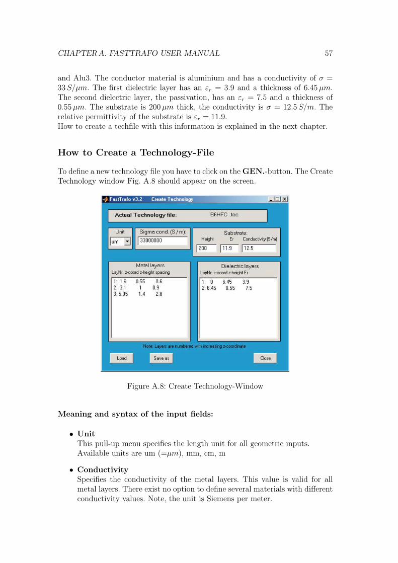
How to Create a Technology-File
To define a new technology file you have to click on the GEN.-button. The CreateTechnology window Fig. A.8 should appear on the screen.
Figure A.8: Create Technology-Window
Meaning and syntax of the input fields:
• UnitThis pull-up menu specifies the length unit for all geometric inputs.Available units are um (=µm), mm, cm, m
• ConductivitySpecifies the conductivity of the metal layers. This value is valid for allmetal layers. There exist no option to define several materials with differentconductivity values. Note, the unit is Siemens per meter.
58 CHAPTER A. FASTTRAFO USER MANUAL
• SubstrateThese parameters specify the substrate propertiesHeight: Height of the substrate.Er: Relative permittivity of the substrate.Conductivity: Conductivity of the substrate. Note, the unit is Siemensper meter. In the literature the substrate conductivity is often replaced bythe resistivity in Ωcm. Use following relation to convert the units.
[S/m]=100/[Ωcm]
• Metal layersThis field contains all metal layer relevant data. The input is organizedsimilarly as a matrix. Each row characterizes one metal layer and eachcolumn one parameter, respectively. The first column indicates the layernumber. You have to enter a number followed by a colon. The second columndefines z-coordinate (=distance from the substrate to the metal layer). Thethird column specifies height (thickness of each metal layer). The fourthcolumn specifies minimal lateral spacing between two metal traces placedon the same layer.The following input example is based on the B6HFC-Technology shown inFig. A.7.
Syntax: <layer-number> : <Z-coordinate> <height> <min-spacing>
Example B6HFC Tech
1: 1.6 0.55 0.6
2: 3.1 1 0.9
3: 5.05 1.4 2.8
• Dielectric layersThe field contains all dielectric relevant data. The syntax is similar to theMetal layer field. The following input example is based on the B6HFC-Technology shown in Fig. A.7.
Syntax: <layer-number> : <Z-coordinate> <height> <Er>
Example B6HFC Tech
1: 0 6.45 3.9
2: 6.45 0.55 7.5
• Save asAfter clicking Save as a small box will appear where you can enter thetechnology name. After clicking OK the data will be saved with the en-tered name as a technology file in the directory .../FTRAFO/TECH. Alltechnology files carry the automatically assigned extension .tec.
CHAPTER A. FASTTRAFO USER MANUAL 59
• LoadYou can load previous generated techfiles into the input mask. It is a con-venient way to generate new techfiles based on files that have already beencreated.
• CloseClose the window without saving data.
Results Window
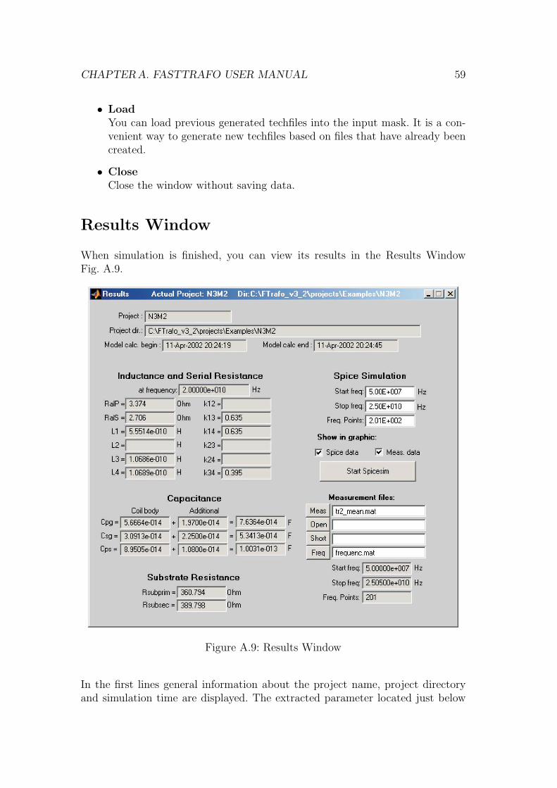
When simulation is finished, you can view its results in the Results WindowFig. A.9.
Figure A.9: Results Window
In the first lines general information about the project name, project directoryand simulation time are displayed. The extracted parameter located just below
60 CHAPTER A. FASTTRAFO USER MANUAL
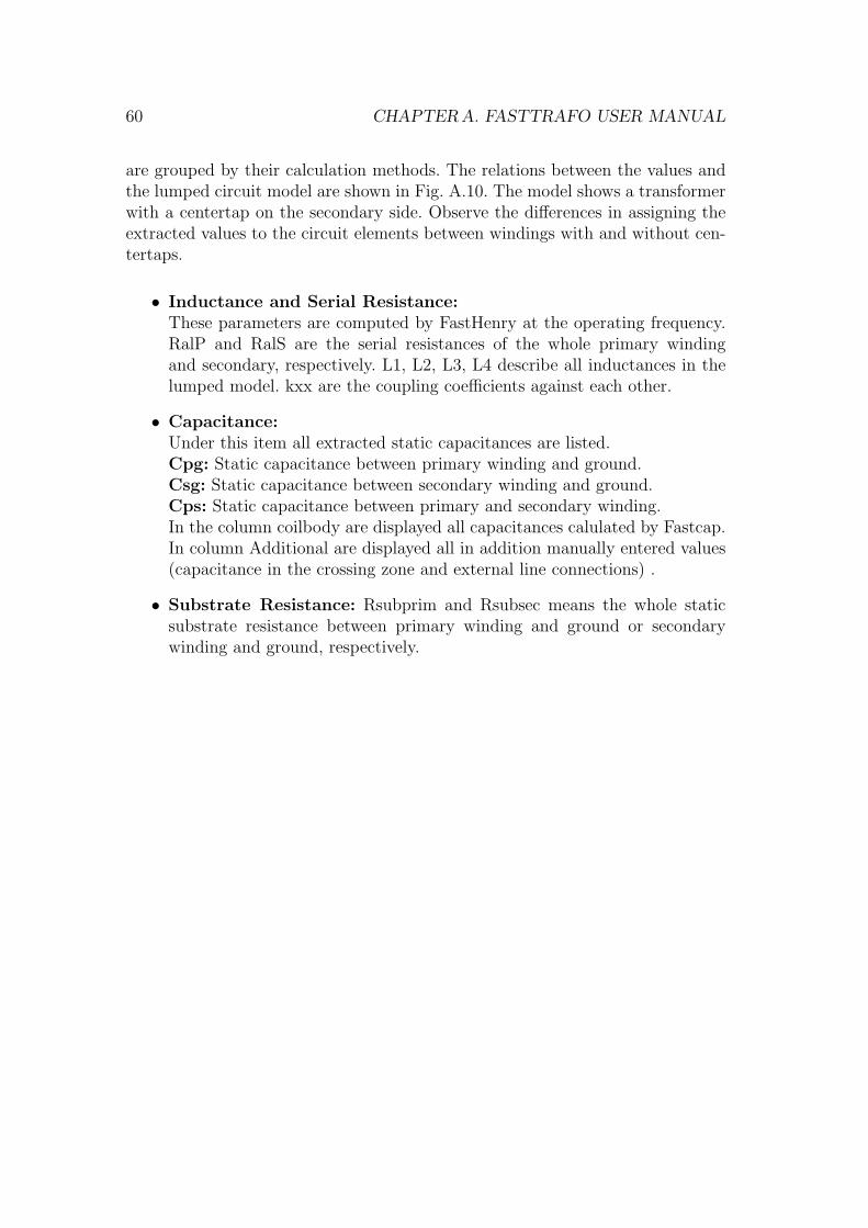
are grouped by their calculation methods. The relations between the values andthe lumped circuit model are shown in Fig. A.10. The model shows a transformerwith a centertap on the secondary side. Observe the differences in assigning theextracted values to the circuit elements between windings with and without cen-tertaps.
• Inductance and Serial Resistance:These parameters are computed by FastHenry at the operating frequency.RalP and RalS are the serial resistances of the whole primary windingand secondary, respectively. L1, L2, L3, L4 describe all inductances in thelumped model. kxx are the coupling coefficients against each other.
• Capacitance:Under this item all extracted static capacitances are listed.Cpg: Static capacitance between primary winding and ground.Csg: Static capacitance between secondary winding and ground.Cps: Static capacitance between primary and secondary winding.In the column coilbody are displayed all capacitances calulated by Fastcap.In column Additional are displayed all in addition manually entered values(capacitance in the crossing zone and external line connections) .
• Substrate Resistance: Rsubprim and Rsubsec means the whole staticsubstrate resistance between primary winding and ground or secondarywinding and ground, respectively.
CHAPTER A. FASTTRAFO USER MANUAL 61
2Rsubprim Cpg/2 RalP L1 Cpg/2 2Rsubprim
Cps/4Cps/4Cps/4
Cps/4
L4 RalS/2 Csg/4 4RsubsecCsg/24Rsubsec RalS/2 L3
2Rsubsec
Csg/2
Primary winding
Secondary winding
P+ P-
S+ S-Secondary center tap
Figure A.10: Equivalent lumped transformer model
62 CHAPTER A. FASTTRAFO USER MANUAL
Spice Simulation
When you have got ALL parameters of the transformer in the results windowyou are able to start a spice simulation by clicking the Start button. Also a filewith the equivalent lumped circuit spice list will be generated and stored to theactual project directory. But at first you have to enter the frequency range ofinterest. The frequency range and number of simulation points within the rangeare specified by the following fields:
Start freq.: Start frequency in HertzStop freq.: Stop frequency in HertzFreq. Points: Specifies the number of linearly equally spaced points betweenstart and stop frequency.
When the spice circuit simulation is complete, three output windows will appearon the screen. The windows contain several plots which are extracted from a singlespice simulation at the given frequency points. The different plots are just attainedby transformations of the scattering, admittance and impedance matrices.
• S-ParameterwindowShows all scattering parameters of the transformer where port1 can be iden-tified as the primary winding and port2 as the secondary winding.
• Z-ParameterwindowZ11, Z22: Input impedances at primary and secondary side when output isopenCoupling Coefficient kps: Coupling between primary and secondaryside
kps =M√LP LS
=
√√√√ (Y −111 − Z11)Z22
Im(Z11)Im(Z22)
Selfinductance:
Lprimary = Im (Z11) /ω
Lsecondary = Im (Z22) /ω
• Y−1-Parameterwindow
Y11−1, Y22
−1: Input impedances at primary and secondary side whenoutput is shorten.
Qualityfactor (output open):
Q = Im (Z11) /Re (Z11)
Qualityfactor (output short):
Q = Im(Y −1
11
)/Re
(Y −1
11
)

CHAPTER A. FASTTRAFO USER MANUAL 63
Adding Measurements
FastTrafo allows you to display measurements delivered by spectrum analyzersand spice simulation data simultaneously. With the field messdata you can ac-tivate or deactivate this feature. So you are able to compare your extracted spicemodel with the measured data. Unfortunately the measured scattering parame-ters must be saved as specific matlab files. No other file formats are supported.The matlab files must be saved in the directory measure which is located in thecreated project directories.
You have to generate two files in matlab:
First file: The file must contain a variable named frequency. Frequency mustbe a 1xn row vector which contains the n frequency points from the measurementin Hz.
Syntax:
frequency=[fpoint1 fpoint2 ... fpointn]
frequency=[1.000 1.005 1.010 1.015 ...]*1e9
Store the variable by using the save command as matfile in the measure directory.
Second file: This file must contain the variables s11, s12, s21, s22. Each vari-able must be a 1xn row vector containing the partially s-parameter. The numberand order of S-parameter sets must match with the frequency vector. The S-parameters must be given in real and imaginary form.
Syntax:
sxx=[value1 value2 ... valuen]
s11=[0.61+0.53i 0.65+0.54i ...]
s12=[ ... ]
s21=[ ... ]
s22=[ ... ]
Store the variables s11, s12, s21, s22 by using the save command as one matfilein the measure directory.When these two files exist in the measure directory you can specify their namesin the result window by clicking the Mess-button (measured S-paramters) andclicking the Freq-button (frequency points).
Tex Documentation
TeX is powerful typesetting system. Tex has the ability to handle complicatedtechnical text and display mathematical formulas. FastTrafo use TeX to produce a
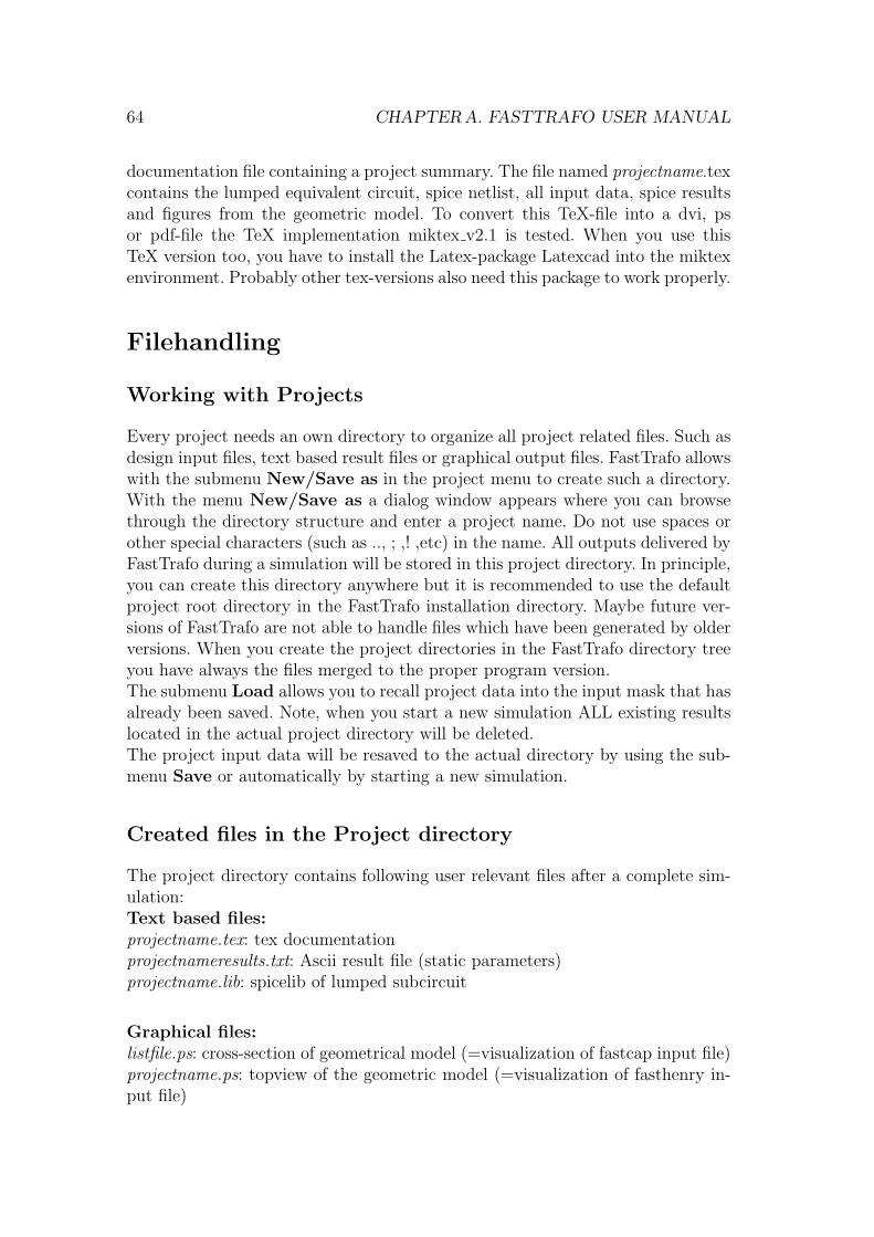
64 CHAPTER A. FASTTRAFO USER MANUAL
documentation file containing a project summary. The file named projectname.texcontains the lumped equivalent circuit, spice netlist, all input data, spice resultsand figures from the geometric model. To convert this TeX-file into a dvi, psor pdf-file the TeX implementation miktex v2.1 is tested. When you use thisTeX version too, you have to install the Latex-package Latexcad into the miktexenvironment. Probably other tex-versions also need this package to work properly.
Filehandling
Working with Projects
Every project needs an own directory to organize all project related files. Such asdesign input files, text based result files or graphical output files. FastTrafo allowswith the submenu New/Save as in the project menu to create such a directory.With the menu New/Save as a dialog window appears where you can browsethrough the directory structure and enter a project name. Do not use spaces orother special characters (such as .., ; ,! ,etc) in the name. All outputs delivered byFastTrafo during a simulation will be stored in this project directory. In principle,you can create this directory anywhere but it is recommended to use the defaultproject root directory in the FastTrafo installation directory. Maybe future ver-sions of FastTrafo are not able to handle files which have been generated by olderversions. When you create the project directories in the FastTrafo directory treeyou have always the files merged to the proper program version.The submenu Load allows you to recall project data into the input mask that hasalready been saved. Note, when you start a new simulation ALL existing resultslocated in the actual project directory will be deleted.The project input data will be resaved to the actual directory by using the sub-menu Save or automatically by starting a new simulation.
Created files in the Project directory
The project directory contains following user relevant files after a complete sim-ulation:Text based files:projectname.tex: tex documentationprojectnameresults.txt: Ascii result file (static parameters)projectname.lib: spicelib of lumped subcircuit
Graphical files:listfile.ps: cross-section of geometrical model (=visualization of fastcap input file)projectname.ps: topview of the geometric model (=visualization of fasthenry in-put file)

CHAPTER A. FASTTRAFO USER MANUAL 65
projectname-S.eps;projectname-Y.eps;projectname-Z.eps: plots created by spicesimulation
FastHenry FastCap input files:projectname.inp: FastHenry input fileground.cap;primary.cap;secondary.cap;listfile.lst: FastCap input files
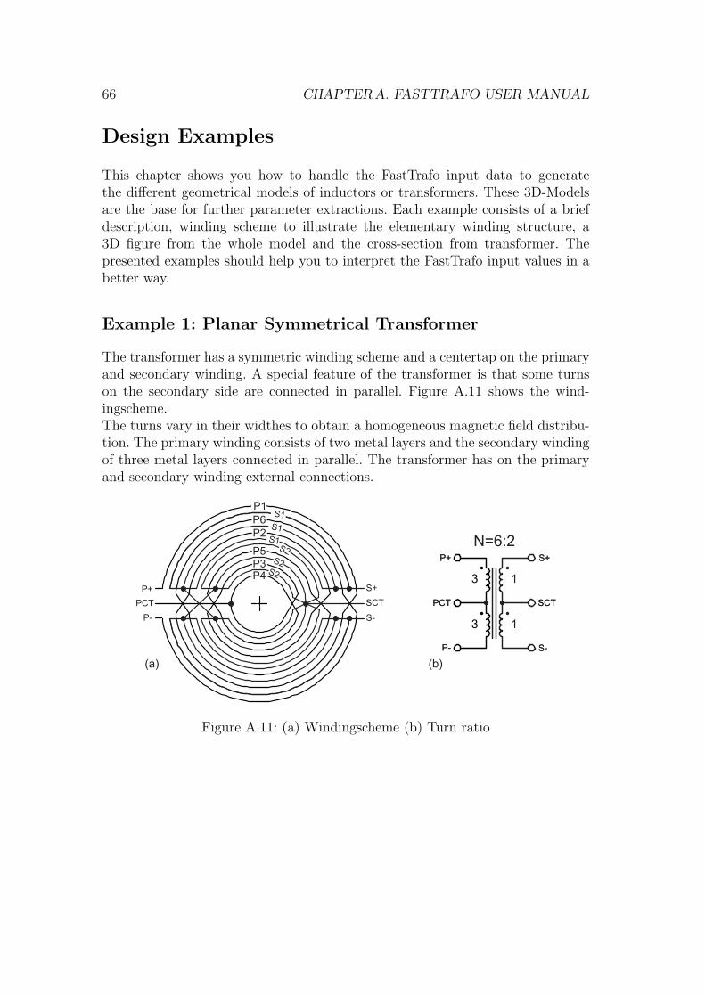
66 CHAPTER A. FASTTRAFO USER MANUAL
Design Examples
This chapter shows you how to handle the FastTrafo input data to generatethe different geometrical models of inductors or transformers. These 3D-Modelsare the base for further parameter extractions. Each example consists of a briefdescription, winding scheme to illustrate the elementary winding structure, a3D figure from the whole model and the cross-section from transformer. Thepresented examples should help you to interpret the FastTrafo input values in abetter way.
Example 1: Planar Symmetrical Transformer
The transformer has a symmetric winding scheme and a centertap on the primaryand secondary winding. A special feature of the transformer is that some turnson the secondary side are connected in parallel. Figure A.11 shows the wind-ingscheme.The turns vary in their widthes to obtain a homogeneous magnetic field distribu-tion. The primary winding consists of two metal layers and the secondary windingof three metal layers connected in parallel. The transformer has on the primaryand secondary winding external connections.
P+
P-
PCT
S1
S1
S1S2
S2S2
S+
SCT
S-
P1
P6
P2
P5P3P4
P-P-
PCTPCT
3
P+P+
3
SCTSCT
S-S-
1
S+S+
1
N=6:2
(a) (b)
Figure A.11: (a) Windingscheme (b) Turn ratio
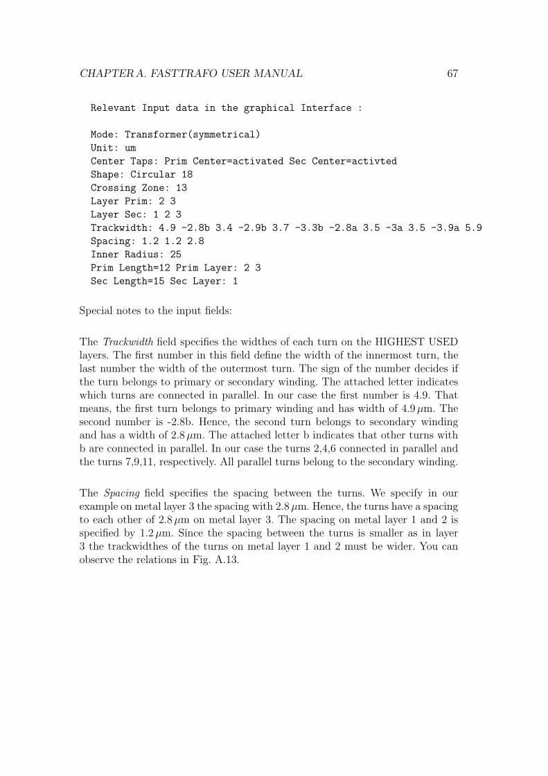
CHAPTER A. FASTTRAFO USER MANUAL 67
Relevant Input data in the graphical Interface :
Mode: Transformer(symmetrical)
Unit: um
Center Taps: Prim Center=activated Sec Center=activted
Shape: Circular 18
Crossing Zone: 13
Layer Prim: 2 3
Layer Sec: 1 2 3
Trackwidth: 4.9 -2.8b 3.4 -2.9b 3.7 -3.3b -2.8a 3.5 -3a 3.5 -3.9a 5.9
Spacing: 1.2 1.2 2.8
Inner Radius: 25
Prim Length=12 Prim Layer: 2 3
Sec Length=15 Sec Layer: 1
Special notes to the input fields:
The Trackwidth field specifies the widthes of each turn on the HIGHEST USEDlayers. The first number in this field define the width of the innermost turn, thelast number the width of the outermost turn. The sign of the number decides ifthe turn belongs to primary or secondary winding. The attached letter indicateswhich turns are connected in parallel. In our case the first number is 4.9. Thatmeans, the first turn belongs to primary winding and has width of 4.9µm. Thesecond number is -2.8b. Hence, the second turn belongs to secondary windingand has a width of 2.8µm. The attached letter b indicates that other turns withb are connected in parallel. In our case the turns 2,4,6 connected in parallel andthe turns 7,9,11, respectively. All parallel turns belong to the secondary winding.
The Spacing field specifies the spacing between the turns. We specify in ourexample on metal layer 3 the spacing with 2.8µm. Hence, the turns have a spacingto each other of 2.8µm on metal layer 3. The spacing on metal layer 1 and 2 isspecified by 1.2µm. Since the spacing between the turns is smaller as in layer3 the trackwidthes of the turns on metal layer 1 and 2 must be wider. You canobserve the relations in Fig. A.13.
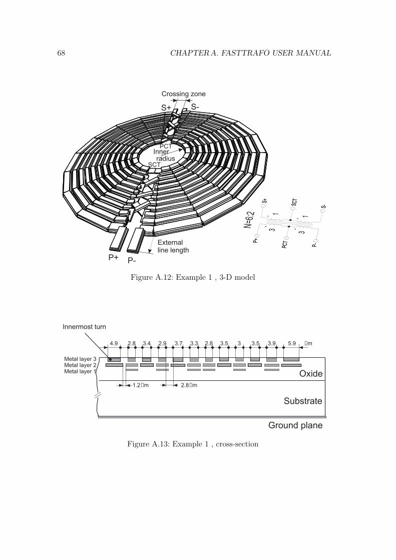
68 CHAPTER A. FASTTRAFO USER MANUAL
P-P-PCT
PCT
3
P+P+
3
SCT
SCT
S-S-
1
S+S+
1
N=6:
2
Crossing zone
radiusInner
Externalline length
P-
SCT
PCT
P+
S+ S-
Figure A.12: Example 1 , 3-D model
Metal layer 3Metal layer 2Metal layer 1
Substrate
Oxide
Ground plane
2.84.9 3.4 2.9 3.7 3.3 2.8 3.5 3 3.5 3.9 5.9 m
1.2m 2.8m
Innermost turn
Figure A.13: Example 1 , cross-section
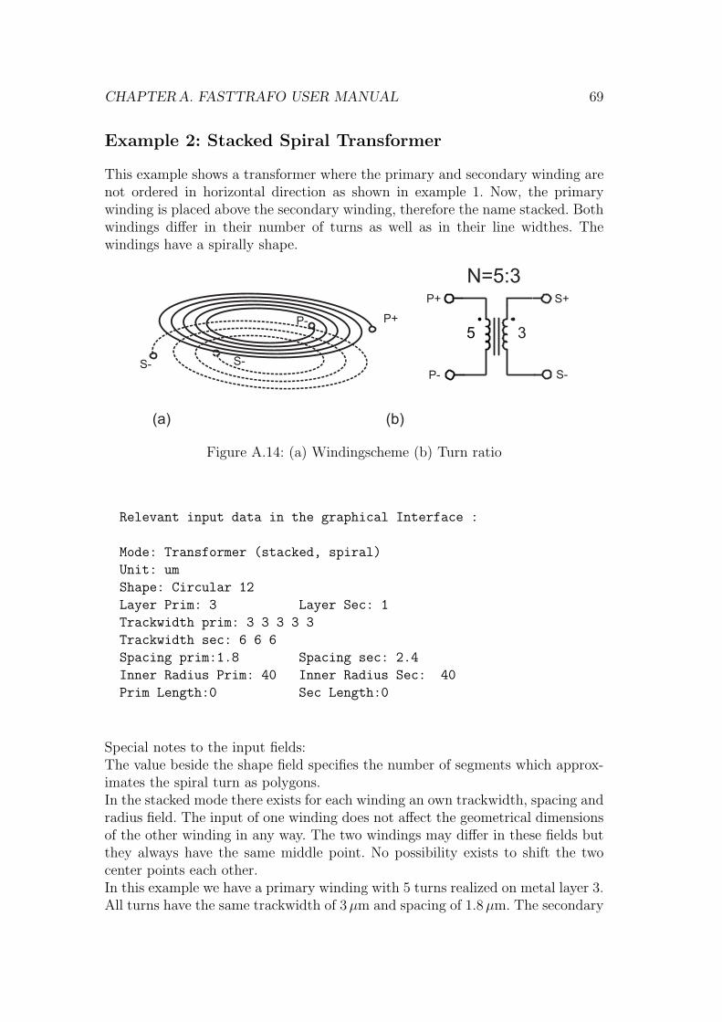
CHAPTER A. FASTTRAFO USER MANUAL 69
Example 2: Stacked Spiral Transformer
This example shows a transformer where the primary and secondary winding arenot ordered in horizontal direction as shown in example 1. Now, the primarywinding is placed above the secondary winding, therefore the name stacked. Bothwindings differ in their number of turns as well as in their line widthes. Thewindings have a spirally shape.
Figure A.14: (a) Windingscheme (b) Turn ratio
Relevant input data in the graphical Interface :
Mode: Transformer (stacked, spiral)
Unit: um
Shape: Circular 12
Layer Prim: 3 Layer Sec: 1
Trackwidth prim: 3 3 3 3 3
Trackwidth sec: 6 6 6
Spacing prim:1.8 Spacing sec: 2.4
Inner Radius Prim: 40 Inner Radius Sec: 40
Prim Length:0 Sec Length:0
Special notes to the input fields:The value beside the shape field specifies the number of segments which approx-imates the spiral turn as polygons.In the stacked mode there exists for each winding an own trackwidth, spacing andradius field. The input of one winding does not affect the geometrical dimensionsof the other winding in any way. The two windings may differ in these fields butthey always have the same middle point. No possibility exists to shift the twocenter points each other.In this example we have a primary winding with 5 turns realized on metal layer 3.All turns have the same trackwidth of 3µm and spacing of 1.8µm. The secondary
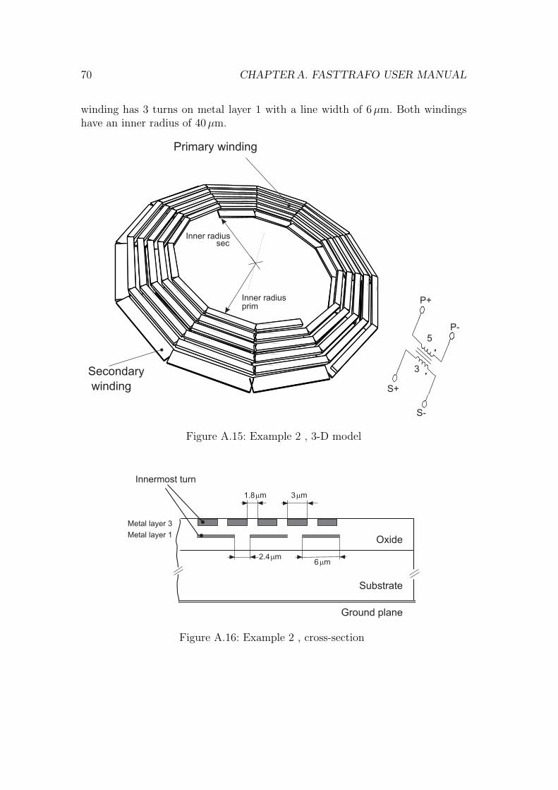
70 CHAPTER A. FASTTRAFO USER MANUAL
winding has 3 turns on metal layer 1 with a line width of 6µm. Both windingshave an inner radius of 40µm.
Primary winding
Secondary
winding
Inner radiussec
Inner radiusprim
3
P+
5
P-
S-
S+
Figure A.15: Example 2 , 3-D model
Innermost turn
Metal layer 3
Metal layer 1Oxide
Ground plane
Substrate
Figure A.16: Example 2 , cross-section
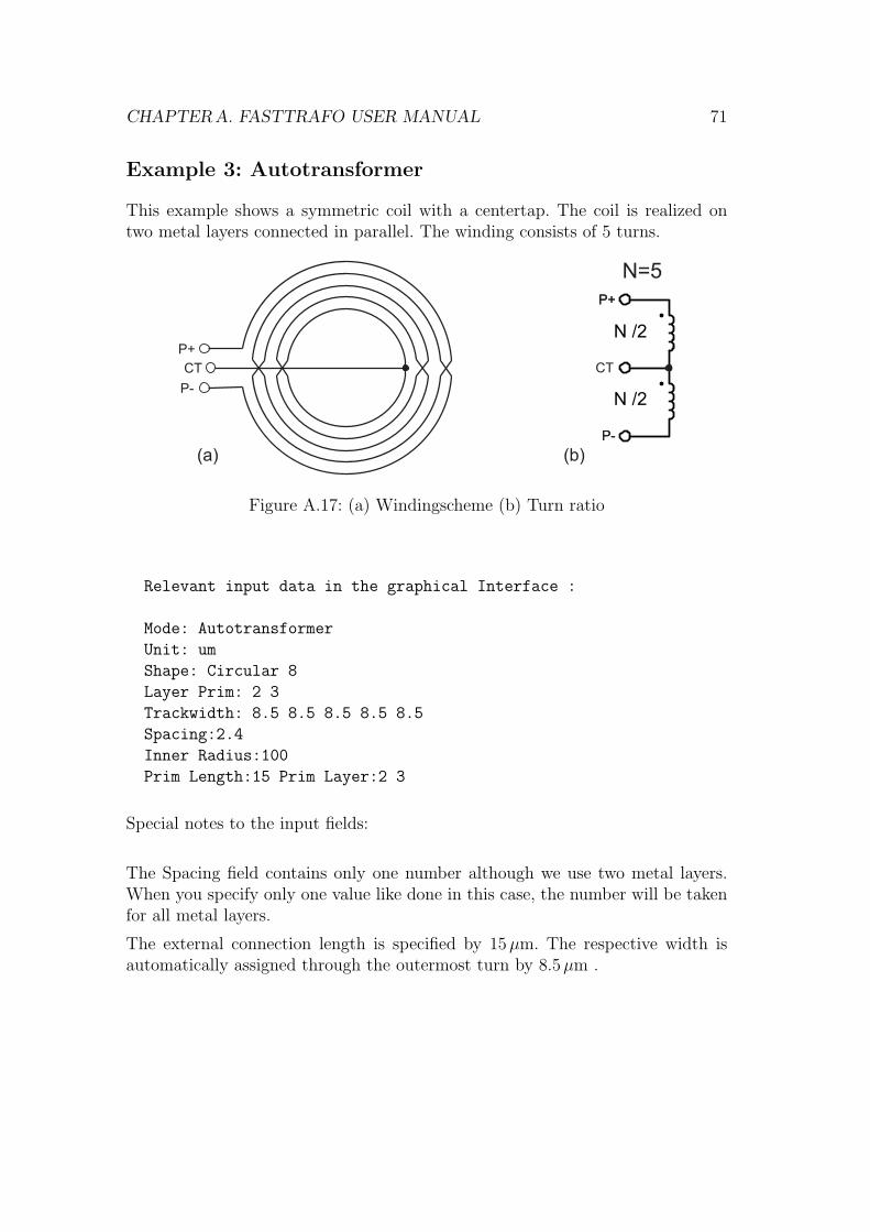
CHAPTER A. FASTTRAFO USER MANUAL 71
Example 3: Autotransformer
This example shows a symmetric coil with a centertap. The coil is realized ontwo metal layers connected in parallel. The winding consists of 5 turns.
P+
P-
CT
P-P-
CT
P+P+
(a) (b)
N=5
N /2
N /2
Figure A.17: (a) Windingscheme (b) Turn ratio
Relevant input data in the graphical Interface :
Mode: Autotransformer
Unit: um
Shape: Circular 8
Layer Prim: 2 3
Trackwidth: 8.5 8.5 8.5 8.5 8.5
Spacing:2.4
Inner Radius:100
Prim Length:15 Prim Layer:2 3
Special notes to the input fields:
The Spacing field contains only one number although we use two metal layers.When you specify only one value like done in this case, the number will be takenfor all metal layers.
The external connection length is specified by 15µm. The respective width isautomatically assigned through the outermost turn by 8.5µm .
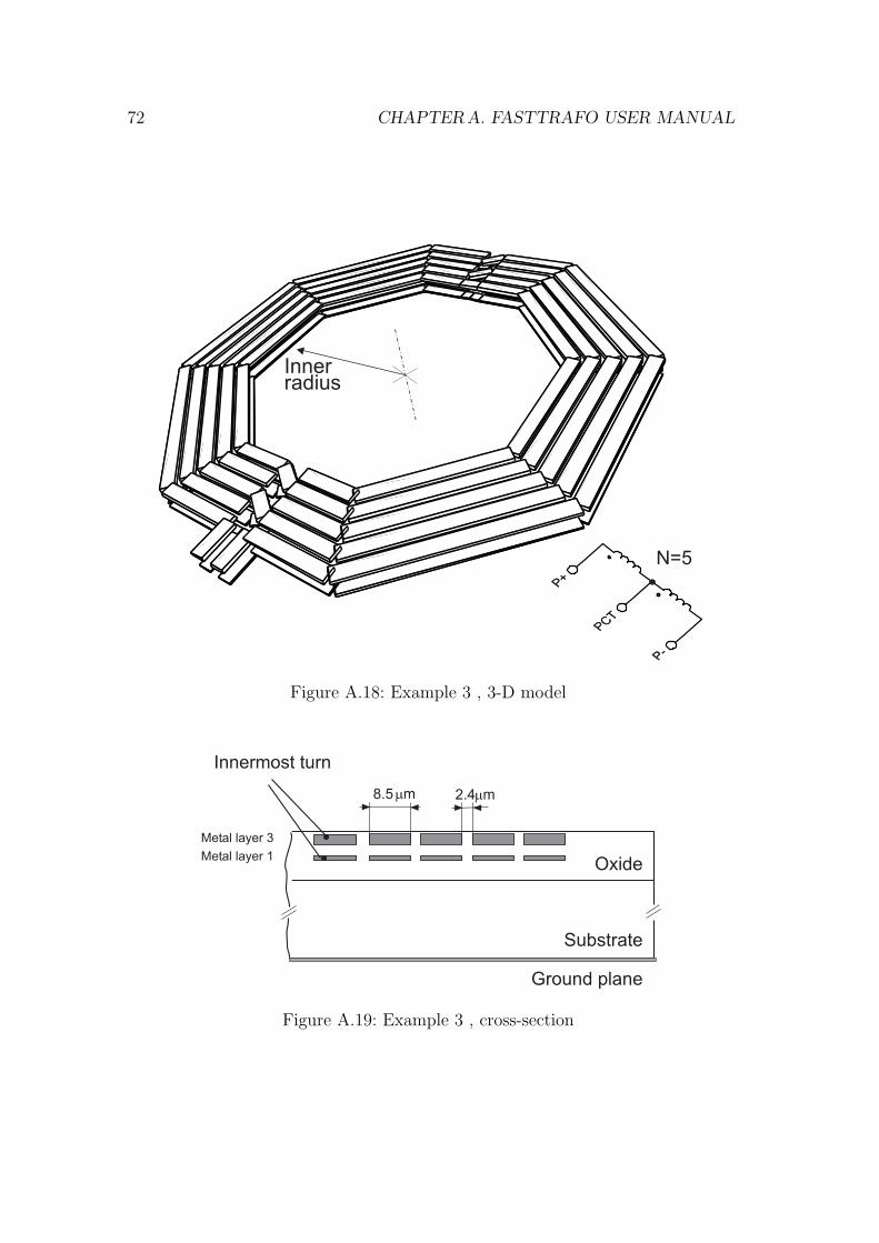
72 CHAPTER A. FASTTRAFO USER MANUAL
Innerradius
P-P-
PCTPCT
P+P+
N=5
Figure A.18: Example 3 , 3-D model
Innermost turn
Metal layer 3
Metal layer 1Oxide
Ground plane
Substrate
Figure A.19: Example 3 , cross-section

CHAPTER A. FASTTRAFO USER MANUAL 73
System Requirements
Hardware Requirements for FastTrafo
Processor:To achieve satisfying processor power for the inductance- and capacitance-simulationa Pentium-II-Processor or a equivalent processor should be installed. For instance,to give you a point of reference by using a Pentium-III-Processor 550 MHz . Thecomputation for design example 1 (Planar Tranformer) lasts about 12 minutes.
RAM:For the inductance-simulation the memory consumption is not a problem. Toavoid a run out of memory during the capacitance-simulation it is recommendedto install at least 256 MB RAM.
Harddisk:The maximum installation requires 35 MB Diskspace.
Optional useful Software for FastTrafo
Latex:To compile the documentation-tex.file a version of Latex and the latexpackageLatexcad is required.
FastModel:FastModel is a 3D viewer that allows you to see in real time the geometric modelswhich are described by FastHenry input files. FastModel can be downloaded athttp://www.fastfieldsolvers.com
Ghostview:This postscript viewer allows you to display figures of the geometric model

74 CHAPTER A. FASTTRAFO USER MANUAL
Bibliography
[Ashby 96] K. B. Ashby and I. A. Koullias, “High Q Inductors for Wire-less Applications in a Complementary Silicon Bipolar Process”,IEEE Journal of Solid-State Circuits, vol. 31, pp. 4–8, Jan 1996.
[Greenhouse 74] H. M. Greenhouse, “Design of Planar Rectangle MicroelectronicInductors”, IEEE Trans. Parts, Hybrids, Packag., vol. 10, pp.101–109, June 1974.
[Grover 46] F. W. Grover, Inductance Calculations, Dover Publications Inc,New York, 1946.
[Kehrer 00] D. Kehrer, Design of Monolithic Integrated Lumped Transform-ers in Silicon-based Technologies up to 20GHz, Institut furNachrichten- und Hochfrequenztechnik der TU Wien, 2000.
[Lofti 95] A. Lofti and F. Lee, “Two Dimensional Skin Effekt in PowerFoils for High-Frequency Applications”, IEEE Trans. on Mag-netics, vol. 31, pp. 1003–1006, March 1995.
[Long 00] J. R. Long, “Monolithic Transformers for Silicon RF IC Design”,IEEE of Solid-State Circuits, vol. 35, pp. 1368–1382, SeP 2000.
[Matlab 01] Matlab, The language of technical computing , MathWorks,1984-2001.
[MIT 92] MIT, FastCap USER’s GUIDE, Massachusetts Institute ofTechnology, 1992.
[MIT 96] MIT, FastHenry USER’s GUIDE, Version 3.0, MassachusettsInstitute of Technology, 1996.
[Niknejad 00] Ali M. Niknejad, Inductors and Transformers for Si RF ICs,Kap, 2000.
[Rabjohn 89] G. G. Rabjohn, Balanced Planar Transformers, United StatesPatent with Patentnumber 4,816,784, 1989.
75
76 BIBLIOGRAPHY
[Yue 98] Yue, “On-Chip Spiral Inductors with Patterned Ground Shieldsfor Si-Based RF IC’s ”, IEEE of Solid-State Circuits, vol. 33,pp. 743–815, May 1998.
[Zinke 95] Brunswig Zinke, Hochfrequenztechnik 1, Springer Lehrbuch,1995.
Acknowlegdements
The work presented was supported by INFINEON Technologies AG, CorporateResearch, Department for High Frequency Circuits, Munich. I would like to ex-press my thanks to Dr. Werner Simbuerger and his team for supporting my thesis.Special thanks are due to my colleagues Dr. Hans-Dieter Wohlmuth and Dipl.Ing.Daniel Kehrer for many informative and helpful discussions.
I would like to take this opportunity to thank my parents for supporting mystudies and for giving valuable advises in any situation of my life.
77


![Centrifugal Distortion and Internal Rotation Analysis in ...zfn.mpdl.mpg.de/data/Reihe_A/36/ZNA-1981-36a-1187.pdf · sources from 8 to 40 GHz [8, 9] was extensively used throughout](https://img.pdfslide.org/doc/110x75/5e9231d27ae99105150d7384/centrifugal-distortion-and-internal-rotation-analysis-in-zfnmpdlmpgdedatareihea36zna-1981-36a-1187pdf.jpg)
![Epigenetic Regulation of Cell Type–Specific Expression Patterns in the Human Mammary ... · 2020. 5. 18. · have been extensively studied in embryonic stem cells (ESCs) [2–4]](https://img.pdfslide.org/doc/110x75/60214a0ccf86db0461289290/epigenetic-regulation-of-cell-typeaspecific-expression-patterns-in-the-human-mammary.jpg)