Embed Size (px)
Citation preview

Electronic Circuits
Handbook for Design and Application
Bearbeitet vonUlrich Tietze, Christoph Schenk, Eberhard Gamm, U Tietze, C Schenk
Neuausgabe 2008. Buch. xlvi, 1543 S.ISBN 978 3 540 00429 5
Format (B x L): 17 x 24,4 cm
Weitere Fachgebiete > Technik > Elektronik > Mikroprozessoren
Zu Inhaltsverzeichnis
schnell und portofrei erhältlich bei
Die Online-Fachbuchhandlung beck-shop.de ist spezialisiert auf Fachbücher, insbesondere Recht, Steuern und Wirtschaft.Im Sortiment finden Sie alle Medien (Bücher, Zeitschriften, CDs, eBooks, etc.) aller Verlage. Ergänzt wird das Programmdurch Services wie Neuerscheinungsdienst oder Zusammenstellungen von Büchern zu Sonderpreisen. Der Shop führt mehr
als 8 Millionen Produkte.
Chapter 27:High-Frequency Amplifiers
Today, in the high- and intermediate-frequency assemblies of telecommunication systems,amplifiers composed of discrete transistors are still used in addition to modern integratedamplifiers. This is particularly the case in high-frequency power amplifiers employed intransmitters. In low-frequency assemblies, on the other hand, only integrated amplifiersare used. The use of discrete transistors is due to the status quo of semiconductor technol-ogy. The development of new semiconductor processes with higher transit frequencies issoon followed by the production of discrete transistors, but the production of integratedcircuits on the basis of a new process does not usually occur until some years later. Fur-thermore, the production of discrete transistors with particularly high transit frequenciesoften makes use of materials or processes which are not (or not yet) suitable for the produc-tion of integrated circuits in the scope of production engineering or for economic reasons.The high growth rate in radio communication systems has, however, boosted the devel-opment of semiconductor processes for high-frequency applications. Integrated circuitson the basis of compound semiconductors such as gallium-arsenide (GaAs) or silicon-germanium (SiGe) can be used up to the GHz range. For applications up to approximately3 GHz bipolar transistors are mainly used, which, in the case of GaAs or SiGe designs,are known as hetero-junction bipolar transistors (HBT). Above 3 GHz, gallium-arsenidejunction FETs or metal-semiconductor field effect transistors (MESFETs) are used.1 Thetransit frequencies range between 50 . . . 100 GHz.
27.1Integrated High-Frequency Amplifiers
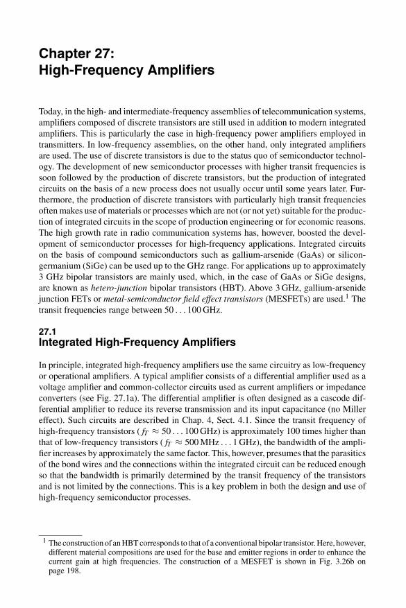
In principle, integrated high-frequency amplifiers use the same circuitry as low-frequencyor operational amplifiers. A typical amplifier consists of a differential amplifier used as avoltage amplifier and common-collector circuits used as current amplifiers or impedanceconverters (see Fig. 27.1a). The differential amplifier is often designed as a cascode dif-ferential amplifier to reduce its reverse transmission and its input capacitance (no Millereffect). Such circuits are described in Chap. 4, Sect. 4.1. Since the transit frequency ofhigh-frequency transistors (fT ≈ 50 . . . 100 GHz) is approximately 100 times higher thanthat of low-frequency transistors (fT ≈ 500 MHz . . . 1 GHz), the bandwidth of the ampli-fier increases by approximately the same factor. This, however, presumes that the parasiticsof the bond wires and the connections within the integrated circuit can be reduced enoughso that the bandwidth is primarily determined by the transit frequency of the transistorsand is not limited by the connections. This is a key problem in both the design and use ofhigh-frequency semiconductor processes.
1 The construction of an HBT corresponds to that of a conventional bipolar transistor. Here, however,different material compositions are used for the base and emitter regions in order to enhance thecurrent gain at high frequencies. The construction of a MESFET is shown in Fig. 3.26b onpage 198.

1362 27. High-Frequency Amplifiers
ri1 0.5...5kΩ
RL 0.5...5 kΩ
RL
vo
vo
vo
vo
v i
v i
v i
v i
ri2 50...500kΩro1 5...50kΩ ro2 50...500 Ω
Rg 50...500 Ω
Rg
i1
i1
IE IE2 I0
i1
vg
vg
vg
vg
Voltageamplifier
Power amplifier
Current amplifier(impedance converter)
IB,A
V b V b
IC,A
a Principle and design of an integrated amplifier
b Principle and design of a matched amplifier with one discrete transistor
R ZL W=
R ZL W=
R Zg W=
R Zg W=
r Zo W=r Zi W=
ZW ZW
ZWZW
v1 = Avvi
v1 = Avvi
io = Al i1
io = Al i1
io = Al i1
Fig. 27.1. Principle construction of high-frequency amplifiers
27.1.1Impedance Matching
Generally, the connecting leads within integrated circuits are so short that they can be con-sidered as ideal connections even in the GHz range;2 therefore, it is not necessary to carryout matching to the characteristic impedance within the circuit. In contrast, the external
2 These are electrically short lines (see Sect. 26.2). In this context the term ideal does not refer tothe losses; these are relatively high in integrated circuits due to the comparably thin metal coatingand the losses in the substrate.

27.1 Integrated High-Frequency Amplifiers 1363
signal-carrying terminals must be matched to the characteristic impedance of the externallines to prevent any reflections. In the ideal case, the circuit is dimensioned such that inputand output impedances, including the parasitic effects of bond wires, connecting limbsand the case, correspond to the characteristic impedance. Otherwise, external componentsor strip lines must be used for impedance matching (see Sect. 26.3).
Figure 27.1a shows typical values of low-frequency input and output resistances ofthe voltage and the current amplifier in an integrated high-frequency amplifier where it isassumed that equivalent amplifiers are employed as signal source and load.
Impedance Matching at the Input
For high frequencies, the input impedance of a differential amplifier is ohmic-capacitivedue to the capacitances of the transistor. Generally, up to around 100 MHz, its value isclearly higher than the usual characteristic impedance ZW = 50 .
A rigorous impedance matching method involves inserting a terminating resistanceR = 2ZW = 100 between the two inputs of the differential amplifier (see Fig. 27.2a);
I0 V B I0
2 I0
a With terminating resistance
b With common-base circuits ( 520 µA for = 5I0 ZW Ω)
vg
vg
vg
vg
R Zg W=
R Zg W=
R Zg W=
R Zg W=
ZW
ZW
ZW
ZW R= 2 ZW
ZW
ZW
Z Zi W>> 2
Fig. 27.2. Impedance matching at the input side of an integrated amplifier

1364 27. High-Frequency Amplifiers
this matches both inputs to ZW = 50 . This method is simple, easy to accomplish witha resistor in the integrated circuit and acts across a wide band. A disadvantage is the poorpower coupling owing to the dissipation of the resistor and the large increase in the noisefigure (see Sect. 27.1.2). Instead of placing a resistance R = 2ZW between the two inputs,each of the two inputs can be connected to ground via a resistance R = ZW . However, thismeans that a galvanic coupling to signal sources with a DC voltage is no longer possibleas the inputs are connected to ground with low resistance. The version with a resistanceR = 2ZW is thus preferred.
As an alternative, common-base circuits can be used for the input stages (see Fig. 27.2b);then, the input impedance corresponds approximately to the transconductance resistance1/gm = VT /I0 of the transistors. With a bias current I0 ≈ 520 mA, this resistance is1/gm ≈ ZW = 50 . In this case, the power coupling is optimal. A disadvantage is thecomparably high noise figure (see Sect. 27.1.2).
Both methods are suitable for frequencies in the MHz range only. In the GHz range, theinfluence of the bond wires, the connecting limbs and the casing have a noticeable effect.The situation can be improved by using loss-free matching networks made up of reactivecomponents or strip lines that must be fitted externally. This will provide an optimumpower coupling with a very low noise figure. In practice, impedance matching focuses lesson optimum power transmission than it does on optimum noise figure, or a compromisebetween both optima. This is described in more detail in Sect. 27.1.2.
Impedance Matching at the Output
Wideband matching of the output impedance of a common-collector circuit to the usualcharacteristic impedance ZW = 50 can be achieved by influencing the output impedanceof the voltage amplifier while taking into consideration the impedance transformation ina common-collector circuit. For the qualitative aspects refer to Fig. 2.105a on page 149and to the case shown in the left portion of Fig. 2.106 where the output impedance of acommon-collector circuit has a wideband ohmic characteristic if the preceding amplifierstage has an ohmic-capacitive output impedance with a cut-off frequency that correspondsto the cut-off frequency ωβ = 2 πfβ of the transistor. Due to secondary effects this type ofmatching can be achieved quantitatively only with the aid of circuit simulation. Again, inthe GHz range, the influence of the bond wires, the connecting limb and the casing showa disturbing effect. In principle, impedance matching remains possible, but not with thewideband effect.
If impedance matching is not possible by influencing the output impedance of thecommon-collector circuit, external matching networks with reactive components or striplines are used.
27.1.2Noise Figure
In Sect. 2.3.4 we showed that the noise figure of a bipolar transistor with a given collectorcurrent IC,A is minimum if the effective source resistance between the base and the emitterterminal reaches its optimum value:
Rg opt =√
R2B + β VT
IC,A
(VT
IC,A
+ 2RB
) RB→0
≈ VT
√β
IC,A
(27.1)

27.1 Integrated High-Frequency Amplifiers 1365
Here, RB is the base spreading resistance and β the current gain of the transistor. For thecollector currents IC,A ≈ 0.1 . . . 1 mA, which are typical of integrated high-frequencycircuits, the source resistance for β ≈ 100 is in the region Rg opt ≈ 260 . . . 2600 . Withlarger collector currents, Rg opt can be further reduced, e.g. to 50 at IC,A = 23 mA andRB = 10 , but the noise figure reaches only a local minimum as shown in Fig. 2.52 onpage 92. This is caused by the base spreading resistance. Very large transistors with verysmall base spreading resistances are used in low-frequency applications which enables theglobal minimum of the noise figure to be nearly reached even with small source resistances.However, in this case the transit frequency of the transistors drops rapidly; thus, in high-frequency applications, this method can be used in exceptional cases only.
In impedance matching at the input side by means of a terminating resistance asshown in Fig. 27.2a, the effective source resistance has the value Rg,eff = Rg||R/2 =ZW/2 = 25 for each of the two transistors in the differential amplifier due to theparallel connection of the external resistances Rg = ZW and the internal terminat-ing resistance R = 2ZW . It is thus clearly lower than the optimum source resistanceRg opt ≈ 260 . . . 2600 . Furthermore, the noise of the terminating resistance causes thenoise figure to become relatively high. With impedance matching at the input side by meansof a common-base circuit as shown in Fig. 27.2b, the effective source resistance has thevalue Rg,eff = Rg = ZW = 50 ; here, too, the noise figure is comparably high.
For impedance matching with reactive components or strip lines, the internal resistanceRg of the signal source can be matched to the input resistance ri of the transistor by means ofa loss-free and noise-free matching network. If we disregard the base spreading resistanceRB , then ri = rBE . For the effective source resistance Rg,eff between the base and emitterterminals this means that Rg,eff = rBE . For rBE = βVT /IC,A and Rg opt the followingrelationship is obtained from (27.1) with RB = 0:
Rg,eff = rBE = Rg opt√
β (27.2)
Thus, with impedance matching, the effective source resistance is higher than the optimumsource resistance by a factor of
√β ≈ 10. This might make the noise figure lower than
that in the configurations with a terminating resistance or a common-base circuit, but it isstill clearly higher than the optimum noise figure.
The optimum noise figure is only obtained when noise matching is performed insteadof power matching. This means that the internal resistance Rg = ZW of the signal sourceis not matched to ri = rBE but to Rg opt = rBE/
√β. Conversely, the input resistance of the
(noise) matched amplifier is no longer ZW but ZW
√β. This leads to the input reflection
factor
r(24.34)
= ZW
√β − ZW
ZW
√β + ZW
=√
β − 1√β + 1
β≈100
≈ 0.82
and a standing wave ratio (SWR):
s(24.42)
= 1 + |r|1 − |r| = √
ββ≈100
≈ 10
In most applications this is not acceptable. Therefore, a compromise between power andnoise matching is used in most practical cases where a low noise figure is of importance.Power matching is generally used if the noise figure is of no importance.
Above f = fT /√
β ≈ fT /10 the optimum source resistance decreases, as can beseen from the equation for Rg opt,RF in Sect. 2.3.4. This does not mean that the matching

1366 27. High-Frequency Amplifiers
methods in Fig. 27.2 can achieve a lower noise figure in this range. Factor Rg,eff /Rg opt
does go down but the minimum noise figure increases as the equation for Fopt,RF inSect. 2.3.4 shows. We will not examine this range more closely as the noise model forbipolar transistors with a transit frequency above 10 GHz as used in Sect. 2.3.4 will onlyallow qualitative statements in this case. The range f > fT /10 is then entirely in the GHzrange and some secondary effects, such as the correlation between the noise sources ofthe transistor, which were disregarded in Sect. 2.3.4, become significant, and the optimumsource impedance is no longer real.
Example: With the help of circuit simulation we have determined the noise figure of thedifferent circuit versions for an integrated amplifier with the transistor parameters in Fig. 4.5on page 278. Owing to the symmetry, we can restrict the calculations to one of the twoinput transistors; Fig. 27.3 shows the corresponding circuits. We use a transistor of size 10and a bias current of IC,A = 1 mA. In the common-base circuit according to Fig. 27.3c, wereduce the bias current to 520 mA in order to achieve impedance matching to ZW = 50 .
a Without matching b With terminating resistance
d With matching network(power matching or noise matching)
c With common-base circuit
– V b – V b
– V b– V b
V b V b
V bV b
vg vg
vg
vg
Rg = Rg opt= 575Ω
Rg = ZW = 50Ω Rg = ZW = 50Ω
Rg = ZW = 50Ω
Rg = ZW = 50Ω
R= 50Ω
1mA1mA
520 µA 1 mA
or
Matchingnetwork
Fig. 27.3. Circuits for a noise figure comparison
27.2 High-Frequency Amplifiers with Discrete Transistors 1367
The base spreading resistance is RB = 50 and the frequency f = 10 MHz. From (27.1)it follows that Rg opt = 575 for IC,A = 1 mA and Rg opt = 867 for IC,A = 520 mA.
The circuit without matching in Fig. 27.3a achieves an optimum noise figure Fopt =1.12 (0.5 dB) for Rg = Rg opt = 575 and F = 1.52 (1.8 dB) for Rg = 50 . Thecircuit with terminating resistance in Fig. 27.3b results in the noise figure F = 2.66(4.2 dB); the noise figure thus clearly increases. A more favourable value is achieved withthe common-base circuit in Fig. 27.3c where F = 1.6 (2 dB). With power matching toRg = ZW = 50 , according to Fig. 27.3d, the value obtained is F = 1.25 (0.97 dB),which is only a factor of 1.1 (0.5 dB) above the optimum value. The optimum noise figureis achieved with noise matching.
If power matching is essential in order to prevent reflections, the circuit with matchingnetwork and power matching according to Fig. 27.3d leads to the lowest noise figure,followed by the common-base circuit in Fig. 27.3c and then the circuit with terminatingresistance in Fig. 27.3b. Without power matching, the circuit with matching network andnoise matching according to Fig. 27.3d is clearly superior to the circuit without matchingin Fig. 27.3a for Rg = 50 with regard to both the noise figure and the reflection factor.
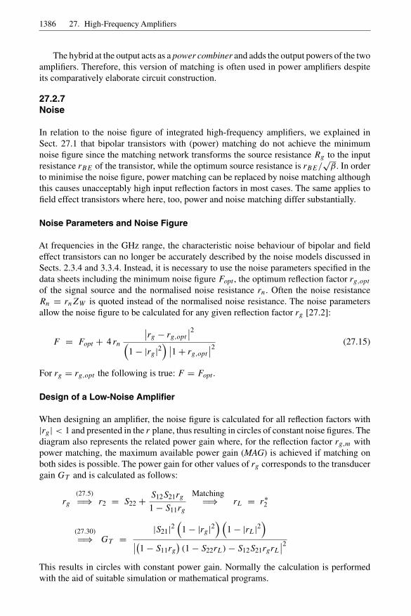
27.2High-Frequency Amplifiers with Discrete Transistors
Figure 27.1b shows the principle design of high-frequency amplifiers made up of discretetransistors. It is clear that the circuit design differs fundamentally from that of the inte-grated amplifier shown in Fig. 27.1a. The actual amplifier consists of a bipolar transistorin common-emitter configuration and circuitry for setting the operating point, which ispresented in Fig. 27.1b, by the two current sources IB,A and IC,A. The practical function-ality will be further described below. Instead of a bipolar transistor, a field effect transistorcan also be used. Coupling capacitances are used in front of and behind the transistor toprevent the operating point from being influenced by the additional circuitry. The networksfor impedance matching to the characteristic impedance of the signal lines include π el-ements (Collins filters) with a series inductance and two shunt capacitances as shown inFig. 27.1b.
27.2.1Generalised Discrete Transistor
The term discrete transistor should not be misunderstood in a limited sense because thecomponents used in practice often contain several transistors and additional resistancesand capacitances in order to simplify the process of setting the operating point. We callthese components generalised discrete transistors.3
Figure 27.4a shows the graphic symbol and the most important versions of a gener-alised discrete transistors without additional components for setting the operating point.A Darlington circuit is often used to enhance the current gain at high frequencies.
Figure 27.4b presents some typical designs with additions for setting the operatingpoint. The version at the left can be used equally well for the Darlington circuits inFig. 27.4a. The resistances provide a voltage feedback which, at sufficiently high-resistive
3 This can be related to the CC operational amplifier which may also be regarded as a generaliseddiscrete transistor (see Sect. 5.5 and Figs. 5.82 to 5.87).

1368 27. High-Frequency Amplifiers
a Symbol and circuit configurations
b Circuit configurations with additional elements for setting the operating point
V b
V b V b
. BGA427e.g e.g. BGA318
Fig. 27.4. Generalised discrete transistor
dimensions, becomes virtually inefficient at high frequencies if the impedance of thecollector-base capacitance falls below the value of the feedback resistor. The externalelement is an inductance which represents an open circuit at the operating frequency andconsequently causes a separation of the signal path and the DC path. The version shown inthe centre of Fig. 27.4b has an additional emitter resistance for current feedback; therefore,it is particularly suitable for wideband amplifiers or amplifiers with a high demand in termsof linearity.
The version shown at the right of Fig. 27.4b consists of a common-emitter circuit withvoltage feedback followed by a common-collector circuit. Strictly speaking, this does notbelong to the group of discrete transistors since, like the integrated amplifier in Fig. 27.1b, itcomprises a voltage amplifier (common-emitter circuit) and a current amplifier (common-collector circuit). Nevertheless, we have included it since it usually comes in a casing that istypical of discrete transistors. The voltage feedback is often operated with two resistancesand one capacitance. Only the resistance, which is directly connected between the base andthe collector, influences the operating point and is used for setting the collector voltageat the operating point. The capacitance is given dimensions such that it functions as ashort circuit at the operating frequency, thus allowing the parallel arrangement of the tworesistances to become effective.

27.2 High-Frequency Amplifiers with Discrete Transistors 1369
The versions shown in Fig. 27.4 are regarded as low-integrated circuits and are termedmonolithic microwave integrated circuits (MMIC). They are made of silicon (Si-MMIC),silicon-germanium (SiGe-MMIC) or gallium-arsenide (GaAs-MMIC) and are suitable forfrequencies of up to 20 GHz.
27.2.2Setting the Operating Point (Biasing)
Generally, the operating point is set in the same way as for low-frequency transistors.However, with high-frequency transistors, one attempts to make the resistances requiredin order to set the operating point ineffective at the operating frequency otherwise theywill have an adverse effect on the gain and noise figure. For this reason, the resistancesare combined with one or more inductances which can be considered short-circuited withregard to setting the operating point, and nearly open-circuited at the operating frequency.
A description of how the operating point is set in a bipolar transistor is given below.The circuits described may equally well be used for field effect transistors.
DC Current Feedback
If we apply the above-mentioned principle to the operating point adjustment with DCcurrent feedback as shown in Fig. 2.75a on page 119, we obtain the circuit design shownin Fig. 27.5a in which high-frequency decoupling is achieved for the base and the collectorof the transistor by means of inductances LB and LC respectively. The collector resistancecan be omitted in this case. Thus, there is no DC voltage drop in the collector circuit sothat this method is particularly suitable for low supply voltages. In extreme situations, onemay remove R1 and R2 and connect the free contact of LB directly to the supply voltage;the transistor then operates with VBE,A = VCE,A. Due to the decoupled base, the noise ofresistors R1 and R2 have only very little influence on the noise figure of the amplifier atthe operating frequency which is a particularly low-noise method for setting the operatingpoint. This is especially the case if an additional capacitance CB is introduced which, at
V b V b
R1 R1
R2 R2RE RECE CECB
Ci
Ci
CiCo
Co Co
LB
LC LC
LC
RCR1
R2
V b V b
V b
a b cWith current feedbackand decoupling of thebase (low noise)
With current feedbackand no decoupling of the base
With voltage feedback
Fig. 27.5. Setting the operating point in high-frequency transistors

1370 27. High-Frequency Amplifiers
the operating frequency, acts almost as a short circuit. Where a slight increase in the noisefigure is not critical, it may not be necessary to decouple the base and thus the circuitshown in Fig. 27.5b may be used.
With an increase in frequency decoupling becomes more and more difficult sincethe characteristics of the inductors used to achieve the required inductance become lessfavourable. In order to make the magnitude of the impedance as high as possible, aninductor with a resonant frequency that is as close as possible to the operating frequencyis used. As a result, the resonant impedance is approximately reached which, however,decreases with an increasing resonant frequency as shown in Fig. 28.4 on page 1406. Forthis reason, in the GHz range, the inductances are replaced by strip lines of the lengthλ/4. These lines are short-circuited for small signals at the end opposite the transistorby capacitance CB or by connecting them to the supply voltage. The end closest to thetransistor then acts as an open circuit.
Particularly problematic is the capacitance CE which, at the operating frequency, mustperform as a short circuit. Here, too, a capacitance with a resonant frequency as close aspossible to the operating frequency is used, whereby doing so results in impedances witha magnitude close to that for the series resistance of the capacitance (typically 0.2 ).However, with increasing resonant frequency, the resonance quality of the capacitancesincreases (see Fig. 28.5 on page 1406), thus making the adjustment more and more difficult.As an alternative, an open-circuited strip line of length λ/4 could be used that acts as ashort circuit at the transistor end but, owing to the unavoidable radiation at the open-endedside (antenna effect), this method is not practical. A short-circuited strip line must alsobe rejected as it provides a short circuit for the DC current and thus short-circuits theresistance RE . Owing to these problems, the DC current feedback is used only in the MHzrange while in the GHz range the emitter terminal of the transistor must be connecteddirectly to ground.
DC Voltage Feedback
Figure 27.5c shows the method of setting the operating point by means of DC voltagefeedback. This is used in many monolithic microwave integrated circuits (see Fig. 27.4b).A collector resistance RC is essential in order to render the feedback effective and to ensurea stable operating point. The collector is decoupled by the inductance LC so that, at theoperating frequency, the output is not loaded by the collector resistance. The base can bedecoupled by adding series inductances to the resistances R1 and R2; however, this methodis not used in practice. A disadvantage is an increase in the noise figure due to the noisecontributions from R1 and R2, but these can be kept low using high-resistive dimensioning.
Automatic Operating Point Control
Amplifiers, whether consisting of integrated circuits or discrete components, are oftenprovided with automatic control of the operating point as shown in Fig. 27.6. Here, thecollector current of the high-frequency transistor T1 is measured from the voltage drop VRC
across the collector resistance RC and compared with a setpoint value VD1. Transistor T2controls the voltage at the base of transistor T1 so that VRC ≈ VD1 ≈ 0.7 V .

27.2 High-Frequency Amplifiers with Discrete Transistors 1371
V b V b
R2V BE1,A R2R1
R1
CB CB
Ci
Co
CC
LB
RB
LC
T1 T1
T2
D2
D2
D1 V D1 V VRC D1D1
T2 LC
RC
IC1,AIB1,A
IE2,A
IR2
RC
V b
a Discrete components b Integrated circuit (e.g. BGC405)
on/off
CC
Fig. 27.6. Automatic operating point control
Let us first look at the circuit in Fig. 27.6a. It follows that:
VRC = (IC1,A + IE2,A
)RC , VBE1,A = IR2R2 , IE2,A
IB2,A≈0
≈ IB1,A + IR2
Consequently:
VRC =(
IC1,A + IB1,A + VBE1,A
R2
)RC
IC1,AIB1,A
≈(
IC1,A + VBE1,A
R2
)RC
If the emitter-base voltage of transistor T2 corresponds approximately to the voltage ofdiode D2, then:
VRC ≈ VD1 ⇒ IC1,A ≈ VD1
RC
− VBE1,A
R2≈ 0, 7 V
(1
RC
− 1
R2
)
R2 RC is typically the case in practice; thus IC1,A ≈ 0.7 V/RC .The control circuit must have a pronounced low-pass characteristic of the first order
to ensure stability; capacitance CB serves this purpose. It is selected such that the cut-offfrequency
fg = 1
2πCB (R2 || rBE1)
is below the operating frequency by a factor of at least 104.Figure 27.6b shows the control of the operating point for an integrated circuit where the
elements LC and CB must be provided externally. The inductance LB is usually replaced bya resistance which slightly shifts the operating point. Resistance RC is usually an externalcomponent so that the bias current can be adjusted. This adjustment is necessary as thebias current, which is optimum in terms of gain and noise figure, depends on the operatingfrequency. Furthermore, the ground connection of resistance R1 is usually accessible fromthe outside so that the amplifier can be turned on and off by a switch.

1372 27. High-Frequency Amplifiers
27.2.3Impedance Matching for a Single-Stage Amplifier
Calculation of the matching networks for an amplifier with a generalised single transistoris complex because the impedances at the input and output port depend on the circuitryconnected to the other port, respectively; this is due to the internal reactive feedback whichalso leads to a non-zero reverse transmission. The calculation is usually based on the Sparameters of the transistor including the circuitry for setting the operating point.
Conditions for Impedance Matching
Figure 27.7 shows a transistor with matching networks and the corresponding reflectionfactors at various positions. Since these points are fully matched, the reflection factors atthe signal source and the load are zero. The matching network at the input side transformsthe reflection factor of the signal source from zero to rg at the transistor input where itmeets the input reflection factor r1 of the transistor. Similarly, the matching network atthe transistor output transforms the reflection factor of the load from zero to rL, whichmeets the output reflection factor r2 of the transistor. For two-sided impedance matching,the respective reflection factors must be conjugate complex to one another:
rg = r∗1 , rL = r∗
2 (27.3)
The related impedances are also conjugate complex to one another:
Zg = ZW
1 + rg
1 − rg
rg=r∗1= ZW
1 + r∗1
1 − r∗1
= Z∗1
ZL = ZW
1 + rL
1 − rL
rL=r∗2= ZW
1 + r∗2
1 − r∗2
= Z∗2
The conditions for power matching are thus met.
Reflection Factors of the Transistor
The reflection factors r1 and r2 of the transistor depend on rL and rg due to the reverse trans-mission (see Fig. 27.8). For the transistor, including the circuitry for setting the operatingpoint, the following is true:[
b1b2
]=
[S11 S12S21 S22
] [a1a2
]
vg
R Zg W=
Z Z= W Z Z= W
R ZL W=
Matchingnetwork
Matchingnetwork
rg
Zg Z2 ZLZ1
rLr1 r2r=0 r=0
=r rL 2*Matching: Matching:=r rg 1
*
*Z ZL 2=*Z Zg 1=
Fig. 27.7. Conditions for impedance matching on both sides

27.2 High-Frequency Amplifiers with Discrete Transistors 1373
a1a b r2 2 L= a b r1 1 g= a2
b1 b1b2 b2
a input reflection factor r1 b Output reflection factor r2
r1 rgrL r2
ZL Zg
Fig. 27.8. Calculating the reflection factors of a connected transistor
With a load with reflection factor rL connected to the output, the input reflection factor r1 isdetermined by inserting the condition a2 = b2rL from Fig. 27.8a and solving the equationfor r1 = b1/a1. Similarly, the output reflection factor r2 with a source with reflectionfactor rg connected to the input is calculated by inserting the condition a1 = b1rg fromFig. 27.8b and solving the equation for r2 = b2/a2. This leads to:
r1 = S11 + S12S21rL
1 − S22rL(27.4)
r2 = S22 + S12S21rg
1 − S11rg(27.5)
Without reverse transmission (S12 = 0), there is no interdependence and the reflectionfactors are r1 = S11 und r2 = S22.
Calculating Impedance Matching
If we insert the conditions (27.3) into (27.4) and (27.5), the reflection factors rg and rL ofthe matched condition are obtained through elaborate calculations [27.1]:
rg,m =B1 ±
√B2
1 − 4|C1|22C1
(27.6)
rL,m =B2 ±
√B2
2 − 4|C2|22C2
(27.7)
The parameters are:
B1 = 1 + |S11|2 − |S22|2 − |S |2
B2 = 1 − |S11|2 + |S22|2 − |S |2
C1 = S11 − SS∗22
C2 = S22 − SS∗11
S = S11S22 − S12S21
In (27.6) and (27.7) the negative sign applies to B1 > 0 or B2 > 0 and the positive sign toB1 < 0 or B2 < 0.
1374 27. High-Frequency Amplifiers
Stability at the Operating Frequency
To ensure that the amplifier is stable, the following must apply:
|rg,m| < 1 , |rL,m| < 1
The real parts of the impedances are thus positive:
ReZg
= Re Z1 > 0 , Re ZL = Re Z2 > 0
It can be demonstrated that this is the case when the stability factor (k factor) is
k = 1 + |S11S22 − S12S21|2 − |S11|2 − |S22|22 |S12S21| > 1 (27.8)
and the secondary conditions
|S12S21| < 1 − |S11|2 , |S12S21| < 1 − |S22|2 (27.9)
are met [27.1].Without reverse transmission (S12 = 0), the k factor is k → ∞. In this case the
secondary conditions require that |S11| < 1 and |S22| < 1, i.e. the real parts of the inputand output impedances of the transistor, including the circuitry for setting the operatingpoint, must be greater than zero. Therefore, a transistor without reverse transmission canbe matched at both sides if the real parts of the impedances are greater than zero. Ifreverse transmission exists (S12 = 0), the secondary conditions are more stringent andthus positive real parts of the input and output impedance are no longer sufficient. In thiscase, however, the condition k > 1 is more crucial than the secondary conditions, i.e. thesecondary conditions are usually met but the condition k > 1 is not.
Calculating Matching Networks
If the conditions (27.8) and (27.9) are met, the matching networks can be determined from(27.6) and (27.7) with the help of the reflection factors rg,m and rL,m. First, the input andoutput impedances of the transistor, whose operating point is set for the matched condition,are calculated:
Z1,m = ZW
1 + r1,m
1 − r1,m
r1,m=r∗g,m= ZW
1 + r∗g,m
1 − r∗g,m
(27.10)
Z2,m = ZW
1 + r2,m
1 − r2,m
r2,m=r∗L,m= ZW
1 + r∗L,m
1 − r∗L,m
(27.11)
Using the procedure described in Sect. 26.3, it is now possible to calculate the matchingnetworks for these impedances.
If conditions (27.8) and (27.9) are not met, a straight-forward procedure is not available.In this case a mismatch at the input or output must be accepted. A problem arises in findingsuitable reflection factors rg and rL for which the mismatch is as small as possible whilethe operation of the system is sufficiently stable. [27.1] describes a procedure on the basisof stability circles which is not discussed in more detail here. A relatively easy procedureis to connect additional load resistances to the input or output of the transistor so that theS parameters meet the conditions of (27.8) and (27.9). However, it depends on the givenapplication whether this yields a better overall result than a possible slight mismatch.
27.2 High-Frequency Amplifiers with Discrete Transistors 1375
Stability Across the Entire Frequency Range
The stability conditions (27.8) and (27.9) ensure stability only at the operating frequencyfor which the matching networks are determined. However, in no way does this guaranteethat the amplifier will be stable at all frequencies. This can be investigated by means of atest setup or by simulating the small-signal frequency response across the entire frequencyrange from zero up to and beyond the transit frequency of the transistor. When measuringthe small-signal frequency response with a network analyser it should be noted that, in thiscase, the amplifier is connected to wide-band circuitry with Rg = ZW and RL = ZW . Inthe actual application, the amplifier may only have narrow-band matching that can causeinstability at frequencies other than the operating frequency, i.e. the stability at the networkanalyser does not necessarily indicate stable operating conditions in the actual application.
Power Gain
For impedance matching on both sides with reactive, i.e. loss-free, matching networks, themaximum available power gain (MAG) [27.1]
MAG =∣∣∣∣S21
S12
∣∣∣∣ (k −√
k2 − 1)
(27.12)
can be determined from (27.8) with the stability factor k > 1. This and other power gainsare described in Sect. 27.4 in more detail.
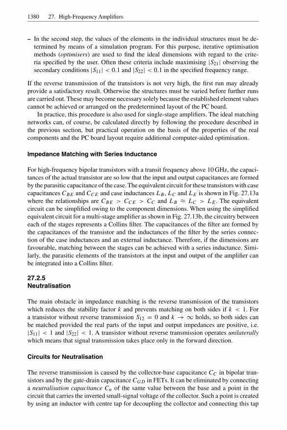
Example: The task is to design a high-frequency amplifier with transistor type BFR93matched at both sides for an operating frequency (centre frequency) fC = 1.88 GHz. Thesupply voltage is to be 3.3 V. We use automatic control of the operating point accordingto Fig. 27.6a with a bias current of IC = 5 mA. For this bias current we obtain a minimumnoise figure as stated in the data sheet.4
Figure 27.9 shows the dimensioned components of a circuit for setting the operatingpoint. The following aspects were taken into consideration:
– Since the input impedance of the transistor is very low (Re S11 < 0 → Re Zi <
50 ), the inductive decoupling of the base is omitted; therefore, the inductance LB ofFig. 27.6a is replaced by a resistor RB = 1 k.
– An inductor with LC = 33 nH and a parallel resonant frequency of approximately1.9 GHz (C ≈ 0, 2 pF) is used for the inductive decoupling of the collector.
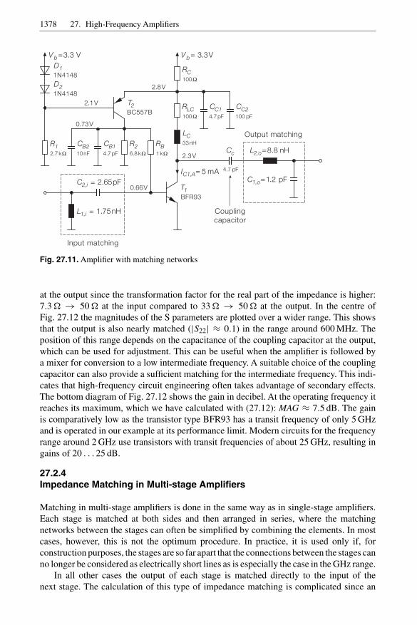
– A resistor RLC = 100 is placed in series with LC so that at frequencies below theoperating frequency it causes losses which increase the k factor in the frequency range100 MHz . . . 1.8 GHz (see Fig. 27.10). This reduces the tendency to oscillate in thisfrequency range.
– For capacitive blocking at the operating frequency, the capacitors CB1 and CC1, whoseseries resonant frequency is approximately 1.9 GHz, are used (C = 4.7 pF, size 0604:L ≈ 1.5 nH).
4 The data sheet also specifies that the maximum transit frequency is reached with IC = 20 mAso that IC = 5 mA is not optimum. However, one should be careful, since the transit frequencyis measured with the output short-circuited, allowing only limited conclusions to be drawn asregards to the power gain that can be achieved with impedance matching on both sides. In anotherdesign, conducted in parallel to this one, for IC = 20 mA a power gain was achieved that was amere 0.2 dB greater, a value which does not warrant the bias quiescent current, especially sincethe noise figure increases significantly.
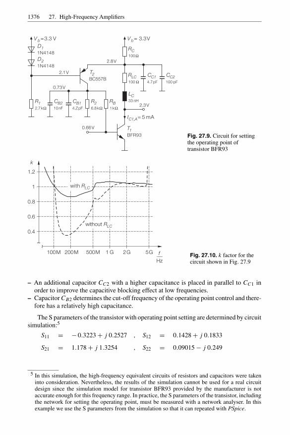
1376 27. High-Frequency Amplifiers
R2 RB
RLCT2
R1 CB1CB2
CC1 CC2
LC
T1
D2
D1 RC
IC1,A= 5 mA
V b=3.3 V V b= 3.3V
1N4148
1N4148
BC557B
BFR93
2.3V
2.8V
2.1V
0.73V
0.66V
1kΩ6.8kΩ2.7kΩ 4.ZpF
4.7pF
33 nH
100 pF
10nF
100 Ω
100Ω
Fig. 27.9. Circuit for settingthe operating point oftransistor BFR93
100M 200M 500M 1 G 5G2G
0.4
0.6
0.8
1.2
1
~
~
fHz
k
with RLC
without RLC
Fig. 27.10. k factor for thecircuit shown in Fig. 27.9
– An additional capacitor CC2 with a higher capacitance is placed in parallel to CC1 inorder to improve the capacitive blocking effect at low frequencies.
– Capacitor CB2 determines the cut-off frequency of the operating point control and there-fore has a relatively high capacitance.
The S parameters of the transistor with operating point setting are determined by circuitsimulation:5
S11 = − 0.3223 + j 0.2527 , S12 = 0.1428 + j 0.1833
S21 = 1.178 + j 1.3254 , S22 = 0.09015 − j 0.249
5 In this simulation, the high-frequency equivalent circuits of resistors and capacitors were takeninto consideration. Nevertheless, the results of the simulation cannot be used for a real circuitdesign since the simulation model for transistor BFR93 provided by the manufacturer is notaccurate enough for this frequency range. In practice, the S parameters of the transistor, includingthe network for setting the operating point, must be measured with a network analyser. In thisexample we use the S parameters from the simulation so that it can repeated with PSpice.

27.2 High-Frequency Amplifiers with Discrete Transistors 1377
With (27.8) it follows that k = 1.05 > 1, i.e. impedance matching on both sides ispossible. The power gain to be expected is obtained with (27.12): MAG = 5.57 ≈ 7.5 dB.Equations (27.6) and (27.7) lead to:
rg,m = − 0.6475 − j 0.402 , rL,m = 0.3791 + j 0.6
Then, using (27.10) and (27.11) we can calculate the input and output impedances of thetransistor with operating point setting in the matched condition:
Z1,m = (7.3 + j 14) , Z2,m = (33 − j 80)
For both impedances, the real part is smaller than ZW = 50 so that matching requires astep-up transformation according to Fig. 26.21a on page 1342.
For matching at the input side we obtain from (26.25) with R = 7.3 and X = 14 :
X1 = ± 20.7 , X2 = ∓ 17.7 − 14
We select the high-pass filter characteristic (X1 > 0, X2 < 0) according to Fig. 26.22b onpage 1343, because then the series capacitance C2 can simultaneously serve as a couplingcapacitor. From
X1 = 20.7 , X2 = − 31.7
it follows with (26.26) that:
L1,i = 1.75 nH , C2,i = 2.65 pF
The additional index i refers to the input side matching.For matching at the output side we obtain from (26.25) with R = 33 and X =
− 80 :
X1 = ± 70 , X2 = ∓ 24 + 80
We now select the low-pass filter characteristic (X1 < 0, X2 > 0) according to Fig. 26.22aon page 1343 so that the overall characteristic is that of a band-pass filter. From
X1 = − 70 , X2 = 104
it follows with (26.26) that:
C1,o = 1.2 pF , L2,o = 8.8 nH
The additional index o refers to matching at the output side. An additional coupling capac-itor is required at the output. We use a 4.7 pF capacitor with a series resonant frequencyof 1.9 GHz which, at the operating frequency fC = 1.88 GHz, it acts as a short-circuit andthus has no influence on the matching effect.
Figure 27.11 shows the amplifier with the two matching networks. The elements ofthe matching networks are ideal; at this stage the design is not ready for practical use. It isnecessary to check at which points inductors and capacitors can be connected and wherestrip lines may be advantageous or are mandatory for functionality of the elements. This isnot discussed any further; please refer to the notes on impedance matching in multi-stageamplifiers in the next section.
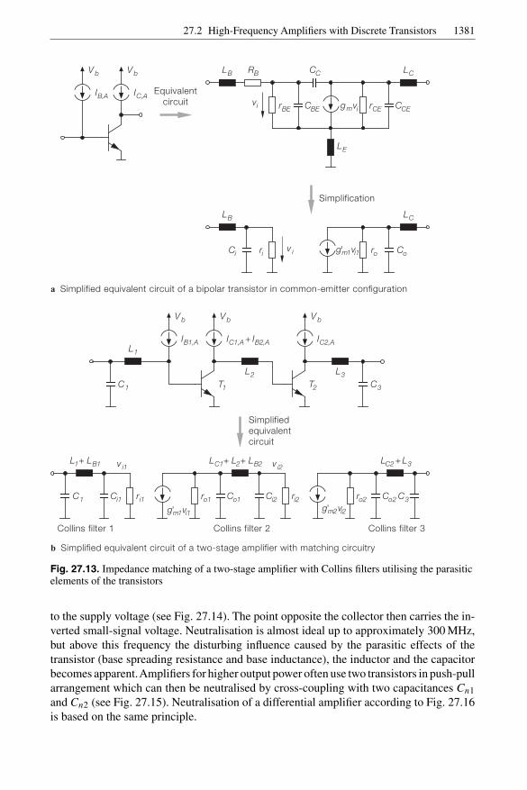
Finally we present the results achieved. The upper part of Fig. 27.12 shows themagnitudes of the S parameters in the matched amplifier at the operating frequencyfC = 1.88 GHz. One can see that matching covers a relatively narrow frequency band.If the requirements |S11| < 0.1 and |S22| < 0.1 hold for the reflection factors, then thebandwidth is approximately 53 MHz. Matching at the input covers a narrower band than
1378 27. High-Frequency Amplifiers
R2 RB
RLCT2
R1 CB1CB2
CC1 CC2
Cc
LC
T1
D2
D1 RC
IC1,A= 5 mA
V b=3.3 V V b= 3.3V
1N4148
1N4148
BC557B
BFR93
2.3V
2.8V
2.1V
0.73V
0.66V
1 kΩ6.8kΩ2.7kΩ 4.7pF
4.7pF
4.7 pF
C1,o=1.2 pFC2,i = 2.65pF
100 pF
10nF
100Ω
100Ω
Couplingcapacitor
33nHL2,o=8.8 nH
L1,i = 1.75nH
Output matching
Input matching
Fig. 27.11. Amplifier with matching networks
at the output since the transformation factor for the real part of the impedance is higher:7.3 → 50 at the input compared to 33 → 50 at the output. In the centre ofFig. 27.12 the magnitudes of the S parameters are plotted over a wider range. This showsthat the output is also nearly matched (|S22| ≈ 0.1) in the range around 600 MHz. Theposition of this range depends on the capacitance of the coupling capacitor at the output,which can be used for adjustment. This can be useful when the amplifier is followed bya mixer for conversion to a low intermediate frequency. A suitable choice of the couplingcapacitor can also provide a sufficient matching for the intermediate frequency. This indi-cates that high-frequency circuit engineering often takes advantage of secondary effects.The bottom diagram of Fig. 27.12 shows the gain in decibel. At the operating frequency itreaches its maximum, which we have calculated with (27.12): MAG ≈ 7.5 dB. The gainis comparatively low as the transistor type BFR93 has a transit frequency of only 5 GHzand is operated in our example at its performance limit. Modern circuits for the frequencyrange around 2 GHz use transistors with transit frequencies of about 25 GHz, resulting ingains of 20 . . . 25 dB.
27.2.4Impedance Matching in Multi-stage Amplifiers
Matching in multi-stage amplifiers is done in the same way as in single-stage amplifiers.Each stage is matched at both sides and then arranged in series, where the matchingnetworks between the stages can often be simplified by combining the elements. In mostcases, however, this is not the optimum procedure. In practice, it is used only if, forconstruction purposes, the stages are so far apart that the connections between the stages canno longer be considered as electrically short lines as is especially the case in the GHz range.
In all other cases the output of each stage is matched directly to the input of thenext stage. The calculation of this type of impedance matching is complicated since an

27.2 High-Frequency Amplifiers with Discrete Transistors 1379
1.6 G
100M
100 M
50M
50 M
200M
200 M
500M
500 M
1.7G
1G
1G
1.8G 1.9G 2.1G 2.2G
5G
5G
2G
2G
2G
0.4
0.4
– 10
– 20
– 30
– 40
0.2
0.2
0.10
0
0.6
0.6
0
0.8
0.8
10
1
1
~~
fHz
fHz
fHz
S21
S22
S22
S11
S11
S12
S12
S21
S21
2.5
2.5
2
2
1.5
1.5
1
1
0.5
0.5
0
0
B(0,1) 53MHz
S21
S21
S21
S21
S21
S11
S11
S11
S11S22 S22
S22
S22
S12
S12
S12
~
~
dB
7.5
Fig. 27.12. S parameters of the amplifier in Fig. 27.11
amplifier with n stages, including n + 1 matching networks (input side, output side andn − 1 networks between the stages), are interdependent owing to the reverse transmissionof the transistors. The procedure is divided into two steps:
– In the first step, structures must be selected that, in principle, allow impedance matchingon the basis of the S parameters of the individual transistors. This must include all wiringthat is required for construction, i.e. the PC board layout of the amplifier must be roughlyoutlined.
1380 27. High-Frequency Amplifiers
– In the second step, the values of the elements in the individual structures must be de-termined by means of a simulation program. For this purpose, iterative optimisationmethods (optimisers) are used to find the ideal dimensions with regard to the crite-ria specified by the user. Often these criteria include maximising |S21| observing thesecondary conditions |S11| < 0.1 and |S22| < 0.1 in the specified frequency range.
If the reverse transmission of the transistors is not very high, the first run may alreadyprovide a satisfactory result. Otherwise the structures must be varied before further runsare carried out. These may become necessary solely because the established element valuescannot be achieved or arranged on the predetermined layout of the PC board.
In practice, this procedure is also used for single-stage amplifiers. The ideal matchingnetworks can, of course, be calculated directly by following the procedure described inthe previous section, but practical operation on the basis of the properties of the realcomponents and the PC board layout require additional computer-aided optimisation.
Impedance Matching with Series Inductance
For high-frequency bipolar transistors with a transit frequency above 10 GHz, the capaci-tances of the actual transistor are so low that the input and output capacitances are formedby the parasitic capacitance of the case. The equivalent circuit for these transistors with casecapacitances CBE and CCE and case inductances LB , LC and LE is shown in Fig. 27.13awhere the relationships are CBE > CCE > CC and LB ≈ LC > LE . The equivalentcircuit can be simplified owing to the component dimensions. When using the simplifiedequivalent circuit for a multi-stage amplifier as shown in Fig. 27.13b, the circuitry betweeneach of the stages represents a Collins filter. The capacitances of the filter are formed bythe capacitances of the transistor and the inductances of the filter by the series connec-tion of the case inductances and an external inductance. Therefore, if the dimensions arefavourable, matching between the stages can be achieved with a series inductance. Simi-larly, the parasitic elements of the transistors at the input and output of the amplifier canbe integrated into a Collins filter.
27.2.5Neutralisation
The main obstacle in impedance matching is the reverse transmission of the transistorswhich reduces the stability factor k and prevents matching on both sides if k < 1. Fora transistor without reverse transmission S12 = 0 and k → ∞ holds, so both sides canbe matched provided the real parts of the input and output impedances are positive, i.e.|S11| < 1 and |S22| < 1. A transistor without reverse transmission operates unilaterallywhich means that signal transmission takes place only in the forward direction.
Circuits for Neutralisation
The reverse transmission is caused by the collector-base capacitance CC in bipolar tran-sistors and by the gate-drain capacitance CGD in FETs. It can be eliminated by connectinga neutralisation capacitance Cn of the same value between the base and a point in thecircuit that carries the inverted small-signal voltage of the collector. Such a point is createdby using an inductor with centre tap for decoupling the collector and connecting this tap
27.2 High-Frequency Amplifiers with Discrete Transistors 1381
IB,A
IB1,A
V b
V b
V b
V b V b
T2T1
IC,A
IC1,A + IB2,A IC2,A
rBE
ri
ri1 ri2
rCE
ro
ro1 ro2
CBE CCE
Ci
Ci1 Ci2
Co
Co1 Co2
CCRBLB
LB
L + L1 B1 L + LC2 3L +C1 L + L2 B2
L2 L3
C3
C3
L1
C1
C1
LC
LC
LE
gmvi
i1
vi
v i
v i1 v i2
Equivalentcircuit
Simplification
a Simplified equivalent circuit of a bipolar transistor in common-emitter configuration
b Simplified equivalent circuit of a two-stage amplifier with matching circuitry
Simplified equivalentcircuit
Collins filter 3Collins filter 2Collins filter 1
g'm1 v
i1 g'm1 v i2 g'm2 v
Fig. 27.13. Impedance matching of a two-stage amplifier with Collins filters utilising the parasiticelements of the transistors
to the supply voltage (see Fig. 27.14). The point opposite the collector then carries the in-verted small-signal voltage. Neutralisation is almost ideal up to approximately 300 MHz,but above this frequency the disturbing influence caused by the parasitic effects of thetransistor (base spreading resistance and base inductance), the inductor and the capacitorbecomes apparent.Amplifiers for higher output power often use two transistors in push-pullarrangement which can then be neutralised by cross-coupling with two capacitances Cn1and Cn2 (see Fig. 27.15). Neutralisation of a differential amplifier according to Fig. 27.16is based on the same principle.

1382 27. High-Frequency Amplifiers
Co
L1a
L1b
CC
C Cn C
Ci
R2
R1
RE CE
V bV b
vC
-vC
Fig. 27.14. Neutralisation of a transistor
CC1
CC2
CB
Cn1 Cn2
R2
T2
L1
L2a
L3a
L3b
L4
L2b
R1
T1
RE1
RE2
CE1
CE2
Vb
Vb
Fig. 27.15. Neutralisation of a push-pull circuit

27.2 High-Frequency Amplifiers with Discrete Transistors 1383
CC1 CC2
Cn1
Cn2
T2T1
Fig. 27.16. Neutralisation of a differentialamplifier
Power Gain in the Case of Neutralisation
Neutralisation and two-sided impedance matching produce the highest possible powergain, known as unilateral power gain [27.1]:
U =1
2
∣∣∣∣S21
S12− 1
∣∣∣∣2
k
∣∣∣∣S21
S12
∣∣∣∣ − Re
S21
S12
(27.13)
Here, the S parameters of the transistor without neutralisation and the stability factor k
from (27.8) on page 1374 are to be inserted. However, the S parameters of the neutralisedtransistor can also be used, making S12,n = 0 and leading to:6
U = |S21,n|2(1 − |S11,n|2
) (1 − |S22,n|2
)
27.2.6Special Circuits for Improved Impedance Matching
If the methods described so far fail to provide acceptable matching, circulators or 90hybrids can be used to improve matching. This is the case, for example, if noise matchingis carried out at the input of an amplifier in order to minimise the noise figure and at thesame time the lowest possible reflection factor is required.
Impedance Matching with Circulators
A circulator is a transmission-asymmetric multi-port element. In practice, 3-port circula-tors are used exclusively, which are suitable for frequencies in the GHz range and achievetheir transmission asymmetry by means of premagnetised ferrites [27.1].
6 This relationship is obtained by calculating the transducer gain GT according to (27.30) on page1398 with matching on both sides and without reverse transmission, thus giving us S12 = 0,rg = S∗
11 and rL = S∗22.

1384 27. High-Frequency Amplifiers
An ideal 3-port circulator is characterised by b1
b2b3
= ej ϕ
0 0 1
1 0 00 1 0
a1
a2a3
(27.14)
where a1, a2, a3 are the incoming and b1, b2, b3 the reflected waves at the three ports. Thecirculator is fully matched, thus S11,C = S22,C = S33,C = 0. The incident waves aretransmitted to the next port in the order 1 → 2 → 3 → 1 and simultaneously undergoa rotation with the angle ϕ. Transmission asymmetry is seen in the asymmetry of the Smatrix where S12,C = S21,C , S13,C = S31,C and S23,C = S32,C .
Figure 27.17 shows a non-matched amplifier (S11,A = 0, S22,A = 0) provided witha circulator at the input and the output. The directional orientation of the circulators isindicated by arrows in the diagrams. Let us first look at the circulator at the input andassume the non-limiting condition ϕ = 0 which ensures that the wave a1 coming from thesignal source is passed on to the amplifier unaltered:
b2 = S21,C a1
ϕ=0= a1
Wave a2 = S11,A b2, which is reflected at the amplifier input, is then transferred to theterminating resistance ZW at port 3:
b3 = S32,C a2 = S32,C S11,A S21,C a1
ϕ=0= S11,A a1
Here, the wave is absorbed without reflection. This means that no incident wave occurs atport 3 and thus no reflected wave at port 1:
a3 = 0 ⇒ b1 = S13,C a3 = 0
This causes the reflection factor at the input to be zero:
S11 = b1
a1
b1=0= 0
The functional principle of this matching method is based on the fact that a wave reflected atthe input of the amplifier does not reach the signal source but is absorbed in the terminatingresistance. In practice, this requires a circulator with very favourable characteristics andequally good termination at port 3. The circulator at the output of the amplifier operates inthe same fashion.
In practice, only one circulator is normally used to improve the reflection factor of theamplifier. In low-noise amplifiers, the circulator is used at the input side to correct anyexisting input mismatch in the case of noise matching. The next section will describe noise
a1 a4
b3 b6
a2 a5
b2 b5b1 b4
ZW ZW
S11,A 0 S22,A 0
S11= 0
a3 = 0 a6 = 0
S22= 0
≠ ≠
Fig. 27.17. Impedance matching with circulators
27.2 High-Frequency Amplifiers with Discrete Transistors 1385
matching in more detail. Power amplifiers sometimes use a circulator at the output; thecirculator then performs two tasks:
– It reduces the reflection factor S22 at the amplifier output to zero.– It prevents the wave reflected by the load from reaching the output of the amplifier;
instead, the wave is absorbed in the terminating resistance ZW .
The second task is of particular importance as the power amplifier can be destructed bythe reflected wave.
Matching with 90 Hybrids
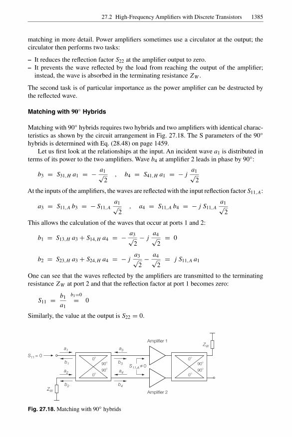
Matching with 90 hybrids requires two hybrids and two amplifiers with identical charac-teristics as shown by the circuit arrangement in Fig. 27.18. The S parameters of the 90hybrids is determined with Eq. (28.48) on page 1459.
Let us first look at the relationships at the input. An incident wave a1 is distributed interms of its power to the two amplifiers. Wave b4 at amplifier 2 leads in phase by 90:
b3 = S31,H a1 = − a1√2
, b4 = S41,H a1 = − ja1√
2
At the inputs of the amplifiers, the waves are reflected with the input reflection factor S11,A:
a3 = S11,A b3 = − S11,A
a1√2
, a4 = S11,A b4 = − j S11,A
a1√2
This allows the calculation of the waves that occur at ports 1 and 2:
b1 = S13,H a3 + S14,H a4 = − a3√2
− ja4√
2= 0
b2 = S23,H a3 + S24,H a4 = − ja3√
2− a4√
2= j S11,A a1
One can see that the waves reflected by the amplifiers are transmitted to the terminatingresistance ZW at port 2 and that the reflection factor at port 1 becomes zero:
S11 = b1
a1
b1=0= 0
Similarly, the value at the output is S22 = 0.
a1
a2 a4
a3
b4
b3b1
b2ZW
ZW
S11 = 0
90O
90O0O
0O90O
90O0O
0O
Amplifier 1
Amplifier 2
S11,A0
Fig. 27.18. Matching with 90 hybrids
1386 27. High-Frequency Amplifiers
The hybrid at the output acts as a power combiner and adds the output powers of the twoamplifiers. Therefore, this version of matching is often used in power amplifiers despiteits comparatively elaborate circuit construction.
27.2.7Noise
In relation to the noise figure of integrated high-frequency amplifiers, we explained inSect. 27.1 that bipolar transistors with (power) matching do not achieve the minimumnoise figure since the matching network transforms the source resistance Rg to the inputresistance rBE of the transistor, while the optimum source resistance is rBE/
√β. In order
to minimise the noise figure, power matching can be replaced by noise matching althoughthis causes unacceptably high input reflection factors in most cases. The same applies tofield effect transistors where here, too, power and noise matching differ substantially.
Noise Parameters and Noise Figure
At frequencies in the GHz range, the characteristic noise behaviour of bipolar and fieldeffect transistors can no longer be accurately described by the noise models discussed inSects. 2.3.4 and 3.3.4. Instead, it is necessary to use the noise parameters specified in thedata sheets including the minimum noise figure Fopt , the optimum reflection factor rg,opt
of the signal source and the normalised noise resistance rn. Often the noise resistanceRn = rnZW is quoted instead of the normalised noise resistance. The noise parametersallow the noise figure to be calculated for any given reflection factor rg [27.2]:
F = Fopt + 4 rn
∣∣rg − rg,opt
∣∣2(1 − |rg|2
) ∣∣1 + rg,opt
∣∣2(27.15)
For rg = rg,opt the following is true: F = Fopt .
Design of a Low-Noise Amplifier
When designing an amplifier, the noise figure is calculated for all reflection factors with|rg| < 1 and presented in the r plane, thus resulting in circles of constant noise figures. Thediagram also represents the related power gain where, for the reflection factor rg,m withpower matching, the maximum available power gain (MAG) is achieved if matching onboth sides is possible. The power gain for other values of rg corresponds to the transducergain GT and is calculated as follows:
rg(27.5)
⇒ r2 = S22 + S12S21rg
1 − S11rg
Matching⇒ rL = r∗2
(27.30)
⇒ GT =|S21|2
(1 − |rg|2
) (1 − |rL|2
)∣∣(1 − S11rg
)(1 − S22rL) − S12S21rgrL
∣∣2
This results in circles with constant power gain. Normally the calculation is performedwith the aid of suitable simulation or mathematical programs.
27.2 High-Frequency Amplifiers with Discrete Transistors 1387
1
Re rg
Im rg
1
MAG
MAG=12 dBFopt =1.6 dB
Fopt
MAG − 1dB
Fopt +1dBFopt + 2dB
Fopt + 3dB
MAG − 2dB
MAG − 3dB
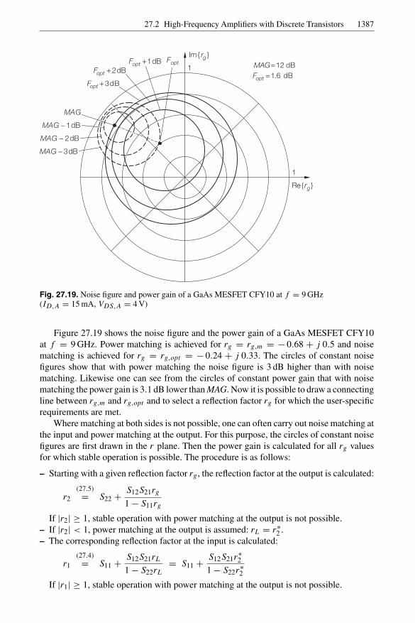
Fig. 27.19. Noise figure and power gain of a GaAs MESFET CFY10 at f = 9 GHz(ID,A = 15 mA, VDS,A = 4 V)
Figure 27.19 shows the noise figure and the power gain of a GaAs MESFET CFY10at f = 9 GHz. Power matching is achieved for rg = rg,m = − 0.68 + j 0.5 and noisematching is achieved for rg = rg,opt = − 0.24 + j 0.33. The circles of constant noisefigures show that with power matching the noise figure is 3 dB higher than with noisematching. Likewise one can see from the circles of constant power gain that with noisematching the power gain is 3.1 dB lower than MAG. Now it is possible to draw a connectingline between rg,m and rg,opt and to select a reflection factor rg for which the user-specificrequirements are met.
Where matching at both sides is not possible, one can often carry out noise matching atthe input and power matching at the output. For this purpose, the circles of constant noisefigures are first drawn in the r plane. Then the power gain is calculated for all rg valuesfor which stable operation is possible. The procedure is as follows:
– Starting with a given reflection factor rg , the reflection factor at the output is calculated:
r2
(27.5)
= S22 + S12S21rg
1 − S11rg
If |r2| ≥ 1, stable operation with power matching at the output is not possible.– If |r2| < 1, power matching at the output is assumed: rL = r∗
2 .– The corresponding reflection factor at the input is calculated:
r1
(27.4)
= S11 + S12S21rL
1 − S22rL= S11 + S12S21r
∗2
1 − S22r∗2
If |r1| ≥ 1, stable operation with power matching at the output is not possible.

1388 27. High-Frequency Amplifiers
1
Re rg
Im rg
1
MSG
Fopt
MSG – 1dB
Fopt +1dB
Fopt + 2dB
Fopt + 3dB
MSG – 2dBMSG – 3dB
MSG – 4dB
Unstable region
MSG = 22dBFopt = 1.3dB
Fig. 27.20. Noise figure and power gain of a bipolar transistor BFP405 at f = 2, 4 GHz(IC,A = 5 mA, VCE,A = 4 V)
– If |r1| < 1, the related transducer gain GT is calculated:
GT =|S21|2
(1 − |rg|2
) (1 − |rL|2
)∣∣(1 − S11rg
)(1 − S22rL) − S12S21rgrL
∣∣2
This results in circles of constant power gain that are limited by a stability border whichis also circular. The stability border is the point at which the maximum stable power gainMSG is obtained; this will be described in more detail in Sect. 27.4.
Figure 27.20 shows the noise figure and the power gain of a bipolar transistor BFP405at f = 2.4 GHz. The stability factor is below one so that power matching at both sides isnot possible. Noise matching is obtained for rg = rg,opt = 0.32 + j 0.25. The circles ofconstant power gain are limited by a stability border at which the maximum stable powergain MSG is reached. The circles of constant power gain show that, with noise matching,the power gain is 3.5 dB below MSG. Likewise the circles of constant noise figure indicatethat for operation with the power gain MSG, the noise figure is 1.8 dB above the minimumnoise figure. A suitable reflection factor rg can now be selected.
If the optimum reflection factor rg,opt with power matching at the output side is locatedinside the instable region, one must do without power matching and shift the stability borderby a suitable choice of rL = r∗
2 until rg,opt is within the stable region.

27.3 Broadband Amplifiers 1389
In practice, optimising the parameters rg and rL in terms of noise, power gain and othercriteria is done by means of simulation or mathematical programs with which non-linearoptimisation processes can be carried out.
27.3Broadband Amplifiers
Amplifiers with a constant gain over an extended frequency range are known as broadbandamplifiers. High-frequency amplifiers are called broadband amplifiers if their bandwidthB is wider than the centre frequency fC thus producing a lower cut-off frequency fL =fC − B/2 < fC/2 and an upper cut-off frequency fU = fC + B/2 > 3fC/2 as well as aratio fU/fL > 3. Sometimes fU/fL > 2 is used as a criterion. The term broadband is givento these amplifiers only because their bandwidth is clearly higher than the bandwidth ofreactively matched amplifiers that are typical of high-frequency applications and in mostcases have a ratio of fU/fL < 1.1. Furthermore, the wideband characteristic of high-frequency amplifiers is also related to impedance matching. Therefore, it is not the −3dBbandwidth that is used as the bandwidth, but the bandwidth within which the magnitudeof the input and output reflection factors remain below a given limit. While reactivelymatched amplifiers usually require reflection factors of |r| < 0.1, broadband amplifiersaccept reflection factors of |r| < 0.2. The less stringent demand reflects the fact thatwideband matching in the MHz or GHz range is much more complicated than the narrow-band reactive matching.
27.3.1Principle of a Broadband Amplifier
The functional principle of a broadband amplifier is based on the fact that a voltage-controlled current source with resistive feedback can be matched at both sides to thecharacteristic impedance ZW . To implement the voltage-controlled current source, one ofthe generalised discrete transistors from Fig. 27.4 on page 1368 is used.7 Figure 27.21shows the principle of a broadband amplifier.
Let us first calculate the gain using the small-signal equivalent circuit shown inFig. 27.22a. The nodal equation at the output is:
vi − vo
R= gmvi + vo
RL
ZW ZW
RR
ZW ZWZW ZWZW ZW
gmvivi
Voltage-controlledcurrent source
Fig. 27.21. Principle of a broadband amplifier
7 The version in the right portion of Fig. 27.4b cannot be used as it has no high-resistance output.

1390 27. High-Frequency Amplifiers
ri
i i io
R R
RL Rg ro
gmvi gmviv iv i vo v i vov i
a Gain and input resistance b Output resistance
Fig. 27.22. Equivalent circuits for calculating the gain as well as the input and output resistancesof a broadband amplifier
This leads to the gain:
A = vo
vi
= RL (1 − gmR)
R + RL
(27.16)
The input current is
ii = vi − vo
R= vi(1 − A)
R
which leads to the input resistance:
ri = vi
ii= R + RL
1 + gmRL
(27.17)
According to Fig. 27.22b, the output current is:
io = vo
R + Rg
+ gmvi = vo
R + Rg
+ gm
Rgvo
R + Rg
This leads to the output resistance:
ro = vo
io= R + Rg
1 + gmRg
(27.18)
We set RL = Rg = ZW and calculate the reflection factors at the input and output:
S11 = ri − ZW
ri − ZW
∣∣∣∣RL=ZW
= R − gmZ2W
R + 2ZW + gmZ2W
(27.19)
S22 = ro − ZW
ro − ZW
∣∣∣∣Rg=ZW
= R − gmZ2W
R + 2ZW + gmZ2W
= S11 (27.20)
The reflection factors S11 and S22 are identical and become zero for:
R = gmZ2W (27.21)
This means that both sides are matched. The forward transmission factor is:
S21 = A
∣∣∣RL=ZW , R=gmZ2
W
= − R
ZW
+ 1 = − gmZW + 1 (27.22)
This is identical to the gain in a circuit which is matched at both ends. It can be influencedonly by means of the transconductance gm as the feedback resistance is linked to thetransconductance. A high transconductance results in a high gain.
27.3 Broadband Amplifiers 1391
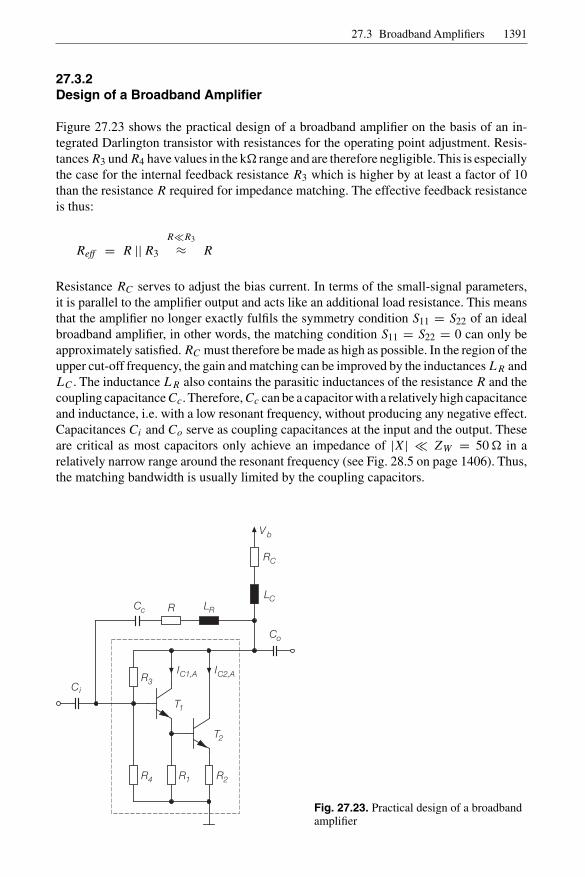
27.3.2Design of a Broadband Amplifier
Figure 27.23 shows the practical design of a broadband amplifier on the basis of an in-tegrated Darlington transistor with resistances for the operating point adjustment. Resis-tances R3 und R4 have values in the k range and are therefore negligible. This is especiallythe case for the internal feedback resistance R3 which is higher by at least a factor of 10than the resistance R required for impedance matching. The effective feedback resistanceis thus:
Reff = R || R3
R R3
≈ R
Resistance RC serves to adjust the bias current. In terms of the small-signal parameters,it is parallel to the amplifier output and acts like an additional load resistance. This meansthat the amplifier no longer exactly fulfils the symmetry condition S11 = S22 of an idealbroadband amplifier, in other words, the matching condition S11 = S22 = 0 can only beapproximately satisfied. RC must therefore be made as high as possible. In the region of theupper cut-off frequency, the gain and matching can be improved by the inductances LR andLC . The inductance LR also contains the parasitic inductances of the resistance R and thecoupling capacitance Cc. Therefore, Cc can be a capacitor with a relatively high capacitanceand inductance, i.e. with a low resonant frequency, without producing any negative effect.Capacitances Ci and Co serve as coupling capacitances at the input and the output. Theseare critical as most capacitors only achieve an impedance of |X| ZW = 50 in arelatively narrow range around the resonant frequency (see Fig. 28.5 on page 1406). Thus,the matching bandwidth is usually limited by the coupling capacitors.
V b
RC
LRCc
Co
C
R1
R3
R4
T1
T2
R2
RLC
IC1,A IC2,A
i
Fig. 27.23. Practical design of a broadbandamplifier

1392 27. High-Frequency Amplifiers
With the help of (27.22) we can use the desired gain to derive the necessary transcon-ductance gm of the voltage-controlled current source which corresponds approximately tothe transconductance of transistor T2 when taking the current feedback via R2 into account:
gm ≈ gm2
1 + gm2R2with gm2 = IC2,A
VT
The selection of the bias current IC2,A determines the maximum output power of theamplifier. In practice, a control signal with an effective value (rms) of up to Ieff ≈ IC2,A/2is useful; the distortion factor then remains below 10%. Consequently, the output powerand the quiescent current are:
Po,max = I 2eff ZW ≈ I 2
C2,AZW
4⇒ IC2,A >
√4 Po,max
ZW
(27.23)
However, the bias current must be high enough to achieve the necessary transconductance:IC2,A ≥ gmVT . In this case, the resistance of the current feedback is:
R2
IC,A>gmVT= 1
gm
− VT
IC2,A
(27.24)
The parasitic inductance of resistor R2 must be as low as possible in order to avoid un-desirable reactive feedback and is of particular importance with values below 20 . If theexpected bandwidth is not achieved in a broadband amplifier with current feedback, thereason is often because the parasitic inductance in the emitter circuit of T2 is too high.
The current feedback via R2 also influences the bandwidth by causing it to increase withincreasing feedback. This is the reason why amplifiers with a particularly wide bandwidthmake use of current feedback even if this is not required on the basis of the output power;typical examples are broadband amplifiers for instrumentation.
Example: In the following, a broadband amplifier is designed according to Fig. 27.23 fora 50 system by using two transistors of the type BFR93 in Darlington configuration (seeFig. 27.24). A gain of A = 16 dB and a maximum output power of Po,max = 0.3 mW =− 5 dBm are required. For the supply voltage we assume Vb = 5 V. The gain is:
|A| = |S21| = 10A [dB]20 dB = 10
16 dB20 dB = 6.3
With (27.22) we obtain the necessary transconductance:
S21 = − gmZW + 1!= 6.3
ZW =50
⇒ gm = 7.3
50 = 146 mS
For the quiescent current of T2 it follows that IC2,A > gmVT = 3.8 mA. With (27.23)we obtain from the maximum output power IC2,A > 4.9 mA. We select IC2,A = 5 mA.The resistor R2 is calculated with (27.24) to be R2 = 1.6 . The resulting small currentfeedback is not implemented for the moment as we must expect a loss in gain owing tosecondary effects.
For the bias current of transistor T1 we select IC1,A = 2 mA since, with smallercurrents, the transit frequency drops rapidly. As the base-emitter voltage of T2 is ap-proximately 0.66 V and the base current IB2,A ≈ 50 mA (current gain approximately100) is negligible compared to IC1,A = 2 mA, the value for the resistor R1 is obtained:
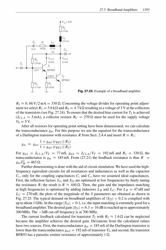
27.3 Broadband Amplifiers 1393
RC
LRCc
Co
Ci
R1
R3
R4
T1
T2
R
LC
BFR93
BFR93
330Ω4.7kΩ
5.6kΩ
10nF 47nH
270 nH
440Ω
270Ω
V b = 5V
IC2,AIC1,A
3V
1.3V
0.66V
2mA 5 mA
Fig. 27.24. Example of a broadband amplifier
R1 ≈ 0, 66 V/2 mA = 330 . Concerning the voltage divider for operating point adjust-ment we select R3 = 5.6 k and R4 = 4.7 k resulting in a voltage of 3 V at the collectorsof the transistors (see Fig. 27.24). To ensure that the desired bias current for T2 is achieved(IC2,A = 5 mA), a collector resistor RC = 270 must be used for the supply voltageVb = 5 V.
After all resistors for operating point setting have been dimensioned, we can calculatethe transconductance gm. For this purpose we use the equation for the transconductanceof a Darlington transistor with resistance R from Sect. 2.4.4 and insert R = R1:
gm ≈ gm11 + gm2 (rBE2 || R1)
1 + gm1 (rBE2 || R1)
For gm1 = IC1,A/VT = 77 mS, gm2 = IC2,A/VT = 192 mS and R1 = 330 , thetransconductance is gm ≈ 185 mS. From (27.21) the feedback resistance is thus R =gmZ2
W = 463 .Further dimensioning is done with the aid of circuit simulation. We have used the high-
frequency equivalent circuits for all resistances and inductances as well as the capacitorCc, only for the coupling capacitances Ci and Co have we assumed ideal capacitances.First, the reflection factors S11 and S22 are optimised at low frequencies by finely tuningthe resistance R; the result is R ≈ 440 . Then, the gain and the impedance matchingat high frequencies is optimised by adding inductors LR and LC . For LR = 47 nH andLC = 270 nH, the plots of the magnitude of the S parameters are obtained as shown inFig. 27.25. The typical demand on broadband amplifiers of |S22| < 0.2 is complied withup to about 1 GHz. In this range |S11| < 0.1, i.e. the input matching is extremely good for abroadband amplifier. The desired gain |S21| = 6.3 = 16 dB is reached up to approximately300 MHz. The −3dB cut-off frequency is at 700 MHz.
The current feedback calculated for transistor T2 with R2 ≈ 1.6 can be neglectedbecause the amplifier achieves the desired gain. Deviations from the calculated valueshave two sources. First, the transconductance gm = 185 mS of the Darlington transistor islower than the transconductance gm2 = 192 mS of transistor T2, and second, the transistorBFR93 has a parasitic emitter resistance of approximately 1 .

1394 27. High-Frequency Amplifiers
100M
100M
50M
50M
20M
20M
200M
200M
500M
500M
1G
1G
5G
5G
2G
2G
0.3
1516.1
13.1
0.2
10
0.1
0
0
0.35
0.25
0.15
5
0.05
~
fHz
fHz
S22
S11 S21
7
2
3
1
0
S21
S11
S11
S22
S22
S21
dB
4
5
6~
~ 700M
Fig. 27.25. S parameters of the broadband amplifier from Fig. 27.24
In practice, the very good overall performance of this amplifier can only be used ina comparatively small frequency band as the coupling capacitances Ci and Co cannotbe given a wide-band low-resistance characteristic. If necessary, several capacitors withstaggered resonant frequencies must be used.
27.4Power Gain
Usually the power gain is specified for high-frequency amplifiers. There are differentdefinitions of gain which relate to different parameters. Some of the related equations onthe basis of S or Y parameters are very complicated. We shall begin by explaining thedefinitions of gain for an ideal amplifier and then extend these to cover a more generalsituation. The complex equations on the basis of S and Y parameters are intended forcomputer-aided evaluations only as manual calculation is very involved.
Figure 27.26 shows the ideal amplifier with the open-circuit gain factor A, the inputresistance ri and the output resistance ro; there is no reverse transmission. The amplifieris operated with a signal source of the internal resistance Rg and a load RL. For furthercalculations we require the overall gain
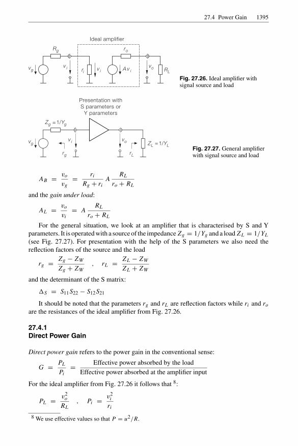
27.4 Power Gain 1395
vgv i v i
vo RL
Rg
ri
ro
Av i
Ideal amplifier
Fig. 27.26. Ideal amplifier withsignal source and load
vgv i vo
Zg g= Y1/
ZL L= Y1/
rLrg
Presentation withS parameters or
Y parameters
Fig. 27.27. General amplifierwith signal source and load
AB = vo
vg
= ri
Rg + riA
RL
ro + RL
and the gain under load:
AL = vo
vi
= ARL
ro + RL
For the general situation, we look at an amplifier that is characterised by S and Yparameters. It is operated with a source of the impedanceZg = 1/Yg and a loadZL = 1/YL
(see Fig. 27.27). For presentation with the help of the S parameters we also need thereflection factors of the source and the load
rg = Zg − ZW
Zg + ZW
, rL = ZL − ZW
ZL + ZW
and the determinant of the S matrix:
S = S11S22 − S12S21
It should be noted that the parameters rg and rL are reflection factors while ri and roare the resistances of the ideal amplifier from Fig. 27.26.
27.4.1Direct Power Gain
Direct power gain refers to the power gain in the conventional sense:
G = PL
Pi
= Effective power absorbed by the load
Effective power absorbed at the amplifier input
For the ideal amplifier from Fig. 27.26 it follows that 8:
PL = v2o
RL
, Pi = v2i
ri
8 We use effective values so that P = u2/R.

1396 27. High-Frequency Amplifiers
This leads to:
G =(
vo
vi
)2ri
RL
= A2L
ri
RL
= A2riRL
(ro + RL)2 (27.25)
The corresponding calculation for the amplifier in Fig. 27.27 leads to:
G =|S21|2
(1 − |rL|2
)1 − |S11|2 + |rL|2
(|S22|2 − |S |2
)− 2 Re
rL
(S22 − SS∗
11
)
= |Y21|2 Re YLRe
Y11 − Y12Y21
Y22YL
|Y22 + YL|2
(27.26)
The direct power gain is independent of the signal source impedance and therefore containsno indication regarding the impedance matching on the input side. Comparison of, say, twoamplifiers that use the same signal source, the same load, and output the same effectivepower to the load reveals that the amplifier with the lower effective input power has ahigher direct power gain. In relation to high-frequency amplifiers, this property is notuseful; therefore, the direct power gain is rarely used in high-frequency engineering.
27.4.2Insertion Gain
Insertion gain is the ratio of the effective powers absorbed by the load with or withoutamplification:
GI = PL
PL,wa
= Effective power absorbed by the load with amplifier
Effective power absorbed by the load without amplifier
Consequently, PL,wa is the effective power which the signal source can deliver directly tothe load. For the ideal amplifier from Fig. 27.26, the following is true:
PL = v2o
RL
, PL,wa = v2gRL(
Rg + RL
)2

27.4 Power Gain 1397
Consequently:
GI =(
vo
vg
)2 (Rg + RL
RL
)2
= A2B
(Rg + RL
RL
)2
=(
ri
Rg + ri
)2
A2(
Rg + RL
ro + RL
)2
(27.27)
The corresponding calculation for the amplifier in Fig. 27.27 leads to:
GI = |S21|2∣∣1 − rgrL
∣∣2∣∣(1 − S11rg)(1 − S22rL) − S12S21rgrL
∣∣2
= |Y21|2 ReYg
Re YL ∣∣Yg + YL
∣∣2∣∣(Y11 + Yg
)(Y22 + YL) − Y12Y21
∣∣2 ∣∣YgYL
∣∣ (27.28)
The insertion gain depends on the impedance of the signal source and the load and thereforetakes the input and output impedance matching into account. However, the maximum gainis generally not reached with matching at both sides. This can be exemplified with the idealamplifier. With two-sided matching, Rg = ri and RL = ro where insertion into (27.27)leads to:
GI,match =(
1
2
)2
A2(
Rg + RL
2RL
)2
This shows that, despite impedance matching at both sides, the insertion gain depends onthe ratio Rg/RL. A constant insertion gain is achieved only in the special case of equalresistances at the input and output, i.e. Rg = ri = ro = RL. Owing to this characteristic,the insertion gain is hardly used.
27.4.3Transducer Gain
Transducer gain specifies the ratio of the effective power absorbed by the load to theavailable (effective) power at the signal source:9
GT = PL
PA,g
= Effective power absorbed by the load
Available power at the signal source
For the ideal amplifier from Fig. 27.26 the following is true:
PL = v2o
RL
, PA,g = v2g
4Rg
This leads to:
GT =(
vo
vg
)2 4Rg
RL
= A2B
4Rg
RL
=(
ri
Rg + ri
)2
A2 4RgRL
(ro + RL)2 (27.29)
9 The available power is an effective power by definition and thus does not have to be explicitlyspecified as being effective.

1398 27. High-Frequency Amplifiers
The corresponding calculation for the amplifier in Fig. 27.27 leads to:
GT =|S21|2
(1 − |rg|2
) (1 − |rL|2
)∣∣(1 − S11rg
)(1 − S22rL) − S12S21rgrL
∣∣2
= 4 |Y21|2 ReYg
Re YL∣∣(Y11 + Yg
)(Y22 + YL) − Y12Y21
∣∣2 (27.30)
The transducer gain depends on the impedance of the signal source and the load andbecomes maximum with impedance matching at both sides. This can be demonstratedwith (27.29):
∂GT
∂Rg
= 0 ,∂GT
∂RL
= 0 ⇒ Rg = ri , RL = ro
Thus, the transducer gain meets the reasonable demands expected of a gain definition.
27.4.4Available Power Gain
Available power gain specifies the ratio of the available powers of the amplifier to thesignal source:
GA = PA,A
PA,g
= Available power of the amplifier
Available power of the signal source
For the ideal amplifier from Fig. 27.26 the following is true:
PA,A = (Avi)2
4ro, PA,g = v2
g
4Rg
This leads to:
GA =(
Avi
vg
)2 Rg
ro=
(ri
Rg + ri
)2
A2 Rg
ro(27.31)
The corresponding calculation for the amplifier in Fig. 27.27 leads to:
GA =|S21|2
(1 − |rg|2
)1 − |S22|2 + |rg|2
(|S11|2 − |S |2
)− 2Re
rg
(S11 − SS∗
22
)
= |Y21|2 ReYg
Re
((Y11 + Yg
)Y22 − Y12Y21
) (Y11 + Yg
) (27.32)
The available power gain is independent of the load and includes no indication with regardto impedance matching at the output side. It is required for noise calculations since theseare based on the available power. The available power gain has already been described inSect. 4.2.4 in connection with the calculation of the noise figure of amplifiers connectedin series (see Eqs. (4.200) and (4.201) on page 460).

27.4 Power Gain 1399
27.4.5Comparison of Gain Definitions
Specific properties of the various gain definitions have already been described in therelevant sections; for this reason, we shall restrict ourselves to a brief comparison here.
Direct power gain G is of no relevance in high-frequency amplifiers since the optimumuse of the available power of the signal source is required and because impedance matchingat the input side necessary for this purpose has no bearing on the direct power gain. Infact, it reaches its maximum if the amplifier absorbs as little power from the signal sourceas possible, i.e. with the poorest possible impedance matching. The direct power gain isrelevant for low-frequency amplifiers since, in these cases, the aim is to achieve the highestpossible voltage gain, which means a minimum load on the signal source. In high-frequencyamplifiers such mismatches are undesirable because of the resulting reflections.
The insertion gain GI is of no real significance for matched amplifiers. This will beexplained for the ideal amplifier in Fig. 27.26. With matching at both sides and differentresistances at input and output a mismatch occurs in the direct connection of signal sourceand load that, in practice, would be corrected by a matching network. For this reason,the two operating modes which are compared in the definition of the insertion gain arenot practical but theoretical alternatives only. With impedance matching at both sides andequal resistances at the input and output, the matched condition (Rg = RL) exists evenwith a direct connection between signal source and load, but in this case the availablepower of the signal source is delivered to the load and the insertion gain GI correspondsto the transducer gain GT .
Due to its properties, the transducer gain GT is the preferred definition of gain in high-frequency engineering and is simply referred to as gain. However, it is not to be confusedwith voltage gain or power gain. Only in the case of impedance matching at both sidesand the same resistances at the input and output are the voltage gain, current gain andtransducer gain identical in their decibel values.
The available power gain GA is required for noise calculations, as mentioned above,but beyond this it is of no importance.
27.4.6Gain with Impedance Matching at Both Sides
With identical resistances at the input and output, matching at both sides means that, for theideal amplifier in Fig. 27.26, Rg = ri = ro = RL = ZW . In this case, all gain definitionsare identical:
G = GI = GT = GA = A2
4= 4 A2
B (27.33)
This is also true for a general amplifier which can be demonstrated by comparing theequations on the basis of the S and Y parameters, taking into account the given matchingconditions. Due to the length of the required calculations, proof thereof is not given here.
Using the S parameters for an amplifier matched at both sides with Rg = RL = ZW
leads to:
S11 = S22 = rg = rL = 0 ⇒ G = GI = GT = GA = |S21|2

1400 27. High-Frequency Amplifiers
This is a simple relationship because the measuring condition RL = ZW for determiningS21 is equal to the operating condition.
When using the Y parameters, the two-sided match to 1/Yg = 1/YL = ZW is reachedwhen certain conditions are met:10
Y11 = Y22 , (Y11Y22 − Y12Y21) Z2W = 1 (27.34)
Then:
G = GI = GT = GA = |Y21|2Z2W
|1 + Y11ZW |2 (27.35)
For an amplifier without reverse transmission Y12 = 0; from the above conditions it followsthat Y11 = Y22 = 1/ZW , i.e. the input resistance ri = 1/Y11and the output resistancero = 1/Y22 must be equal to the characteristic resistance ZW . This case corresponds to theideal amplifier in Fig. 27.26 from which the matching conditions ri = ZW and ro = ZW
can be directly derived if Rg = RL = ZW .
27.4.7Maximum Power Gain with Transistors
Sect. 27.2 showed that a generalised discrete transistor can be matched at both sides if thestability factor is
k = 1 + |S11S22 − S12S21|2 − |S11|2 − |S22|22 |S12S21| > 1 (27.36)
and the secondary conditions
|S12S21| < 1 − |S11|2 , |S12S21| < 1 − |S22|2 (27.37)
are met; here S11, . . . , S22 are the S parameters of the transistor. The conditions for the Yparameters are
k = 2 Re Y11 Re Y22 − Re Y12Y21|Y12Y21| > 1 (27.38)
and:
Re Y11 ≥ 0 , Re Y22 ≥ 0 (27.39)
Maximum Available Power Gain
If matched on both sides, the transistor, including the matching networks, fulfils the con-dition S11,match = S22,match = 0 (see Fig. 27.28). The corresponding power gain is knownas the maximum available power gain (MAG) and is given by [27.1]:
MAG = |S21,match|2 =∣∣∣∣S21
S12
∣∣∣∣ (k −√
k2 − 1)
=∣∣∣∣Y21
Y12
∣∣∣∣ (k −√
k2 − 1)
(27.40)
At high frequencies, MAG is inversely proportional to the square of the frequency:MAG ∼ 1/f 2, which corresponds to a declining rate of 20 dB/decade. This is causedby the frequency dependence of the S and Y parameters.
10 These conditions are determined by calculating theY parameters according to Fig. 24.40 on page1227 from the S parameters while taking into account the condition S11 = S22 = 0.

27.4 Power Gain 1401
vg
R Zg W=
R ZL W=
Matchingnetwork
Matchingnetwork
rg,o rL ,oS11,match=0
|S MAG21,match|2=
S22,match=0
S ,S ,S ,S11 12 21 22,k > 1
Fig. 27.28. Maximum available power gain (MAG) of an amplifier matched at both sides
Maximum Stable Power Gain
At frequencies above approximately a quarter of the transit frequency, the conditions forimpedance matching at both sides are usually met. Below this frequency range k < 1, i.e.matching at both sides is no longer possible; in this case the maximum available powergain is not defined. Only the maximum stable power gain (MSG) can be achieved [27.1]:
MSG =∣∣∣∣S21
S12
∣∣∣∣ =∣∣∣∣Y21
Y12
∣∣∣∣ (27.41)
At low frequencies it is approximately inversely proportional to the frequency: MSG ∼1/f , which corresponds to a rate of decline of 10 dB/decade. When approaching thefrequency for k = 1, the decline rate increases to 20 dB/decade resulting in a smoothtransition between MSG and MAG.
Unilateral Power Gain
The highest achievable power gain is the unilateral power gain (U ):
U =1
2
∣∣∣∣S21
S12− 1
∣∣∣∣2
k
∣∣∣∣S21
S12
∣∣∣∣ − Re
S21
S12
= |Y21 − Y12|24 (Re Y11 Re Y22 − Re Y12Y21) (27.42)
This assumes that the transistor is neutralised by suitable circuitry, i.e. it has no reversetransmission; it then operates unilaterally. Circuits for neutralisation are described inSect. 27.2. At high frequencies, the unilateral power gain is approximately inverselyproportional to the square of the frequency: U ∼ 1/f 2, which corresponds to a declinerate of 20 dB/decade.
Limit Frequencies
The maximum available power gain (MAG) assumes the value 1 or 0 dB at the transitfrequency fT of the transistor. The unilateral power gain (U ) is higher than one even abovethe transit frequency since the reverse transmission is eliminated. The frequency at whichU assumes the value 1 or 0 dB is called the maximum oscillation frequency fmax . Thisrepresents the maximum frequency at which the transistor can be operated as an oscillator.
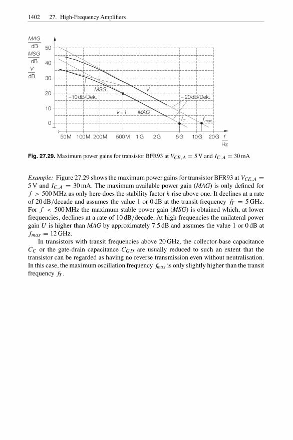
1402 27. High-Frequency Amplifiers
100M50M 200M 500M 1 G 10G 20G5G2G
30
40
50
10
20
0
fHz
VdB
MSGdB
MAGdB
~
~
MAG
MSG
k=1
V10dB/Dek. 20dB/Dek.
fT fmax
– –
Fig. 27.29. Maximum power gains for transistor BFR93 at VCE,A = 5 V and IC,A = 30 mA
Example: Figure 27.29 shows the maximum power gains for transistor BFR93 at VCE,A =5 V and IC,A = 30 mA. The maximum available power gain (MAG) is only defined forf > 500 MHz as only here does the stability factor k rise above one. It declines at a rateof 20 dB/decade and assumes the value 1 or 0 dB at the transit frequency fT = 5 GHz.For f < 500 MHz the maximum stable power gain (MSG) is obtained which, at lowerfrequencies, declines at a rate of 10 dB/decade. At high frequencies the unilateral powergain U is higher than MAG by approximately 7.5 dB and assumes the value 1 or 0 dB atfmax = 12 GHz.
In transistors with transit frequencies above 20 GHz, the collector-base capacitanceCC or the gate-drain capacitance CGD are usually reduced to such an extent that thetransistor can be regarded as having no reverse transmission even without neutralisation.In this case, the maximum oscillation frequency fmax is only slightly higher than the transitfrequency fT .