Embed Size (px)
Citation preview
GEM at CERNGEM at CERN
Leszek Ropelewski CERN PHLeszek Ropelewski CERN PH--DT2DT2--ST & TOTEMST & TOTEM
OutlineOutline
• Introduction to Gas Electron Amplifier• Main Properties• TOTEM• Cylindrical GEM for NA-49 Future• Other Applications and Perspectives• Remarks about Future of GEM Technology at CERN
New and very old resultsLimited to only GDD activities
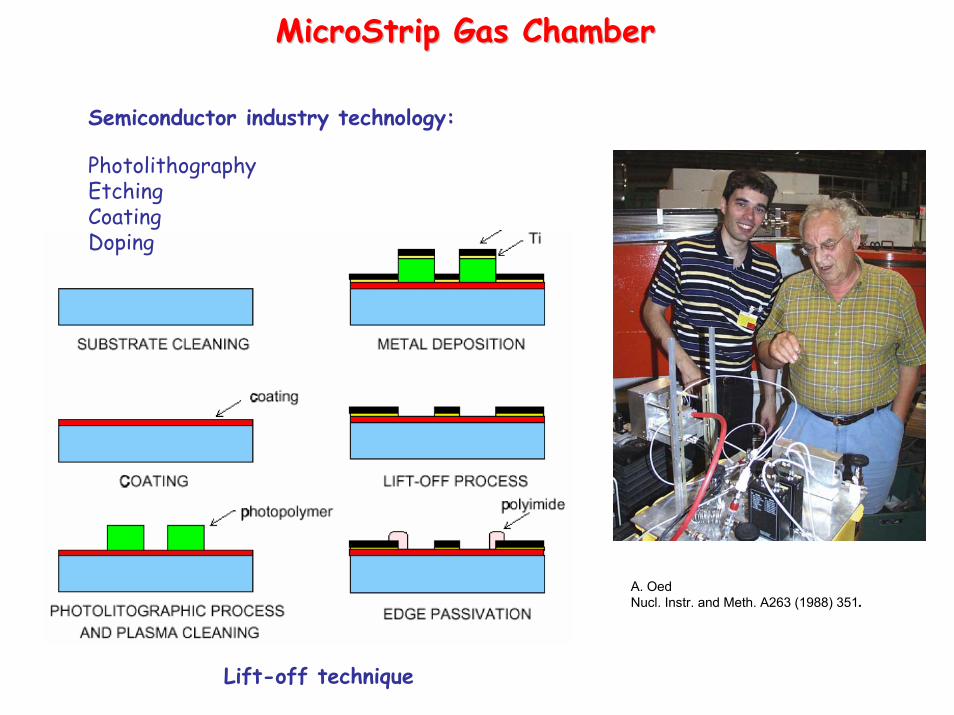
MicroStrip Gas ChamberMicroStrip Gas Chamber
A. OedNucl. Instr. and Meth. A263 (1988) 351.
Lift-off technique
Semiconductor industry technology:
PhotolithographyEtchingCoatingDoping
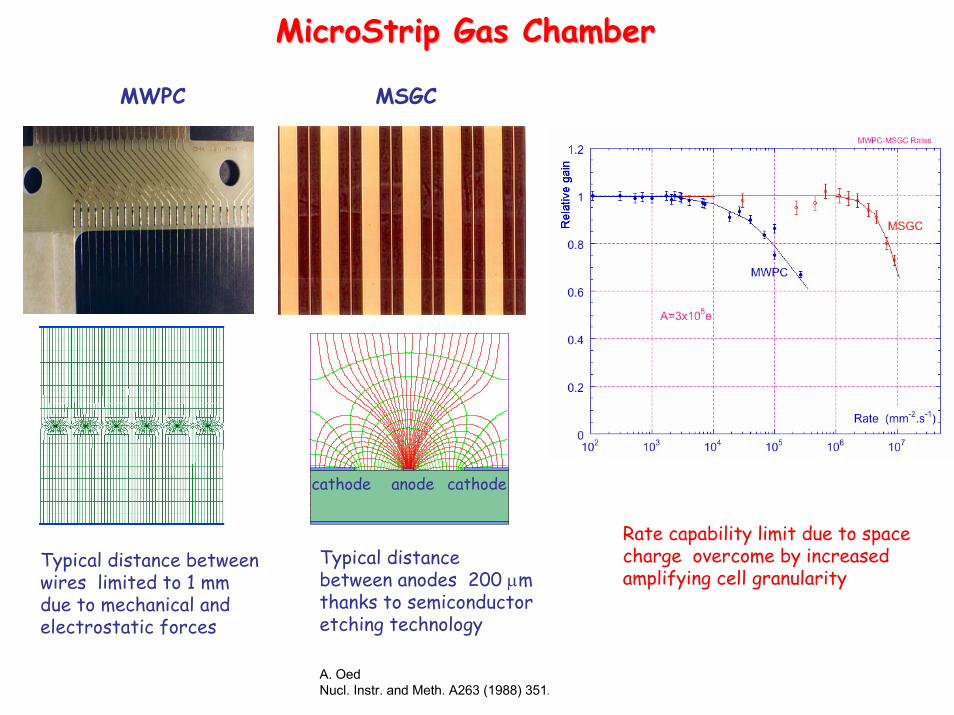
MicroStrip Gas ChamberMicroStrip Gas Chamber
Typical distance betweenwires limited to 1 mmdue to mechanical andelectrostatic forces
Typical distancebetween anodes 200 μmthanks to semiconductoretching technology
MWPC MSGC
anode cathodecathode
A. OedNucl. Instr. and Meth. A263 (1988) 351.
Rate capability limit due to spacecharge overcome by increased amplifying cell granularity
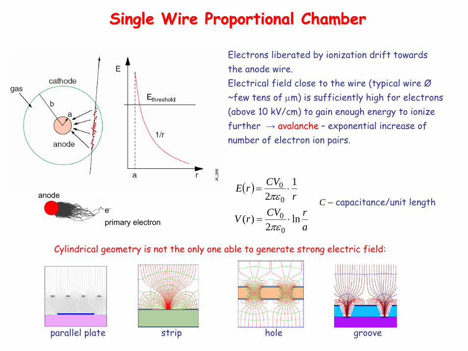
Single Wire Proportional ChamberSingle Wire Proportional Chamber
Electrons liberated by ionization drift towardsthe anode wire. Electrical field close to the wire (typical wire Ø~few tens of μm) is sufficiently high for electrons(above 10 kV/cm) to gain enough energy to ionizefurther → avalanche – exponential increase ofnumber of electron ion pairs.
Cylindrical geometry is not the only one able to generate strong electric field:
parallel plate strip hole groove
( )
arCVrV
rCVrE
ln2
)(
12
0
0
0
0
⋅=
⋅=
πε
πε C – capacitance/unit lengthanode
e-
primary electron
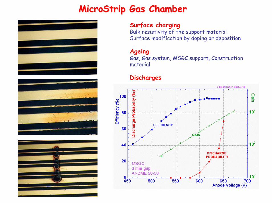
MicroStrip Gas ChamberMicroStrip Gas ChamberSurface chargingBulk resistivity of the support materialSurface modification by doping or deposition
AgeingGas, Gas system, MSGC support, Construction material
Discharges
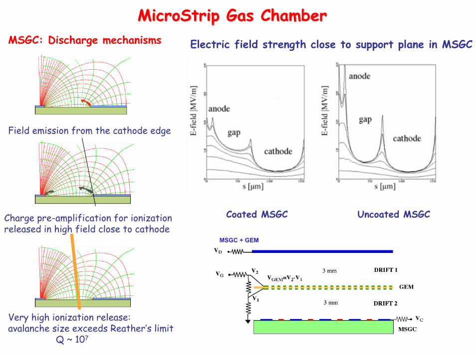
Charge pre-amplification for ionization released in high field close to cathode
MSGC: Discharge mechanisms
Field emission from the cathode edge
Very high ionization release:avalanche size exceeds Reather’s limit
Q ~ 107
MicroStrip Gas ChamberMicroStrip Gas Chamber
Uncoated MSGCCoated MSGC
Electric field strength close to support plane in MSGC
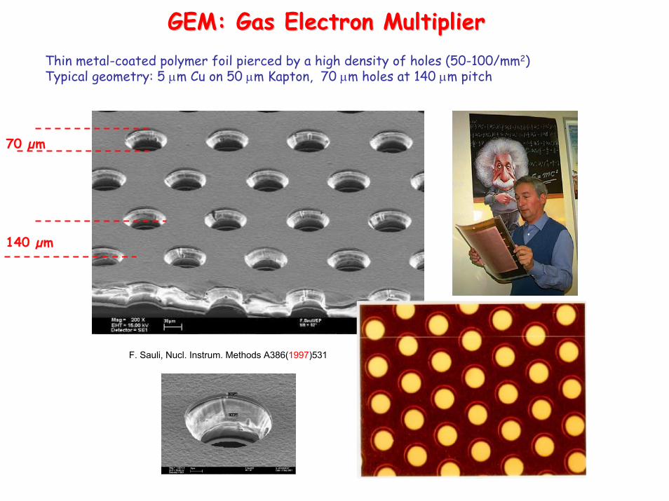
GEM: Gas Electron MultiplierGEM: Gas Electron MultiplierThin metal-coated polymer foil pierced by a high density of holes (50-100/mm2)Typical geometry: 5 μm Cu on 50 μm Kapton, 70 μm holes at 140 μm pitch
F. Sauli, Nucl. Instrum. Methods A386(1997)531
70 µm
140 µm
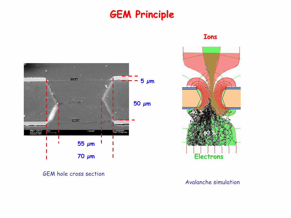
GEM PrincipleGEM Principle
70 µm
55 µm
5 µm
50 µm
GEM hole cross sectionAvalanche simulation
ElectronsElectrons
IonsIons
60 %
40 %
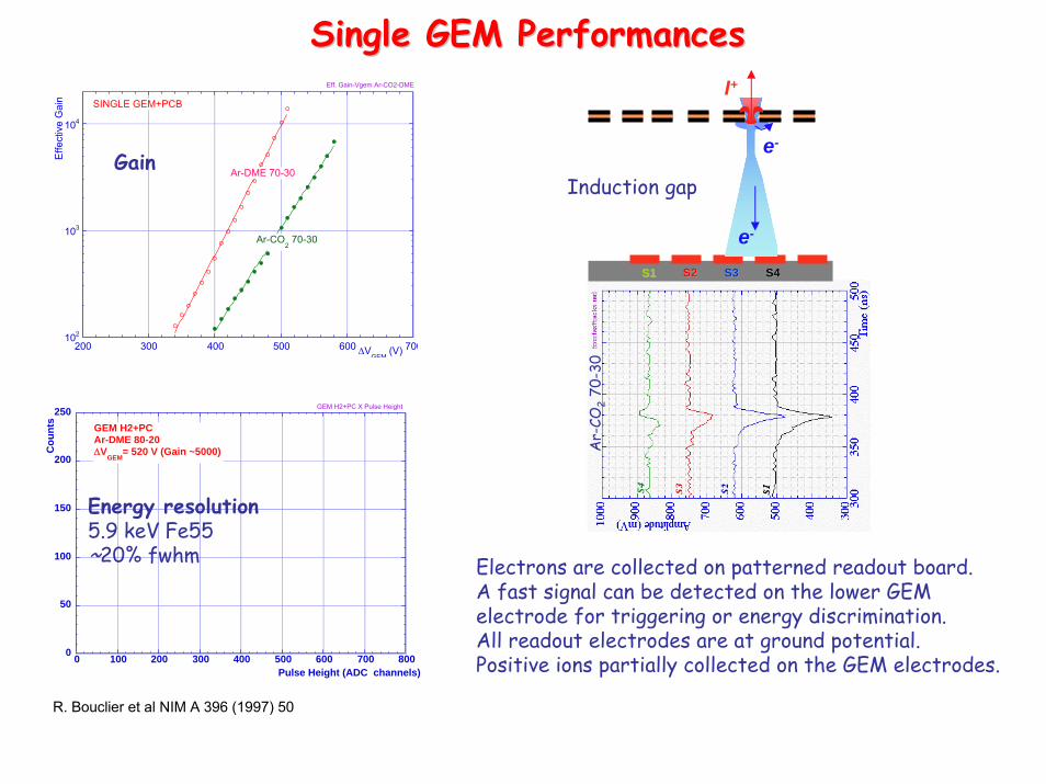
Single GEM PerformancesSingle GEM Performances
0
50
100
150
200
250
0 100 200 300 400 500 600 700 800Pulse Height (ADC channels)
Cou
nts
GEM H2+PCAr-DME 80-20ΔV
GEM= 520 V (Gain ~5000)
GEM H2+PC X Pulse Height
102
103
104
200 300 400 500 600 700ΔVGEM
(V)
SINGLE GEM+PCB
Eff. Gain-Vgem Ar-CO2-DME
Ar-DME 70-30
Ar-CO2 70-30
Effe
ctiv
e G
ain
Gain
R. Bouclier et al NIM A 396 (1997) 50
Energy resolution5.9 keV Fe55~20% fwhm
Ar-
CO2
70-3
0
S4S4S3S3S2S2S1S1
Induction gap
e-
e-
I+
Electrons are collected on patterned readout board. A fast signal can be detected on the lower GEM electrode for triggering or energy discrimination. All readout electrodes are at ground potential.Positive ions partially collected on the GEM electrodes.
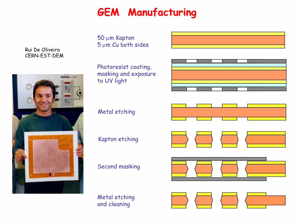
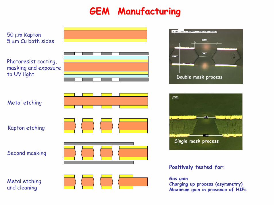
50 μm Kapton5 μm Cu both sides
Photoresist coating, masking and exposureto UV light
Metal etching
Kapton etching
Second masking
Metal etching and cleaning
Rui De OliveiraCERN-EST-DEM
GEM ManufacturingGEM Manufacturing
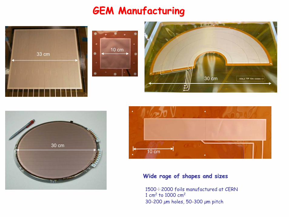
GEM ManufacturingGEM Manufacturing
30 cm
10 cm
33 cm
30 cm
10 cm
1500÷2000 foils manufactured at CERN 1 cm2 to 1000 cm2
30-200 µm holes, 50-300 µm pitch
Wide rage of shapes and sizesWide rage of shapes and sizes
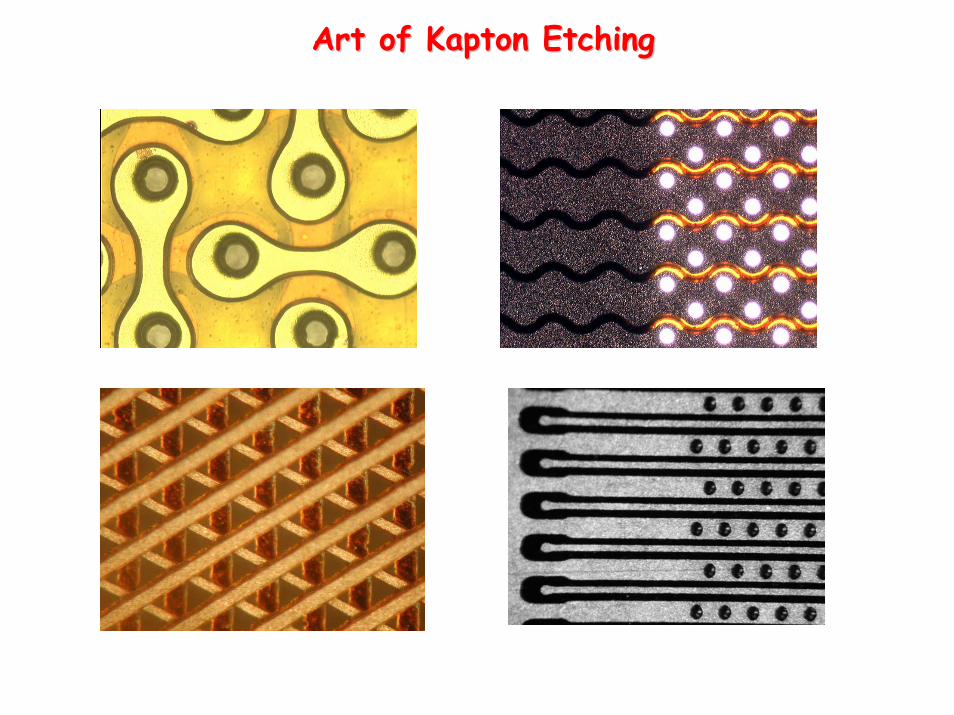
Art of Kapton EtchingArt of Kapton Etching
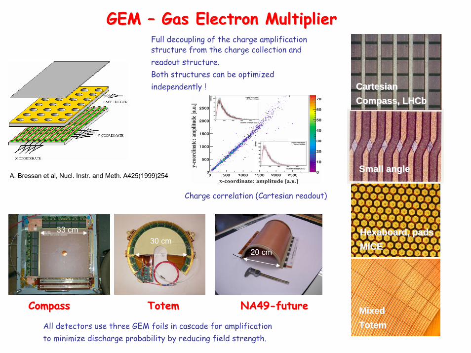
GEM GEM –– Gas Electron MultiplierGas Electron Multiplier
A. Bressan et al, Nucl. Instr. and Meth. A425(1999)254
Full decoupling of the charge amplification structure from the charge collection andreadout structure.Both structures can be optimizedindependently !
All detectors use three GEM foils in cascade for amplificationto minimize discharge probability by reducing field strength.
Cartesian Cartesian Compass, LHCbCompass, LHCb
Small angleSmall angle
Hexaboard, padsHexaboard, padsMICEMICE
MixedMixedTotemTotem
CompassCompass TotemTotem
33 cm
NA49NA49--futurefuture
Charge correlation (Cartesian readout)
30 cm20 cm
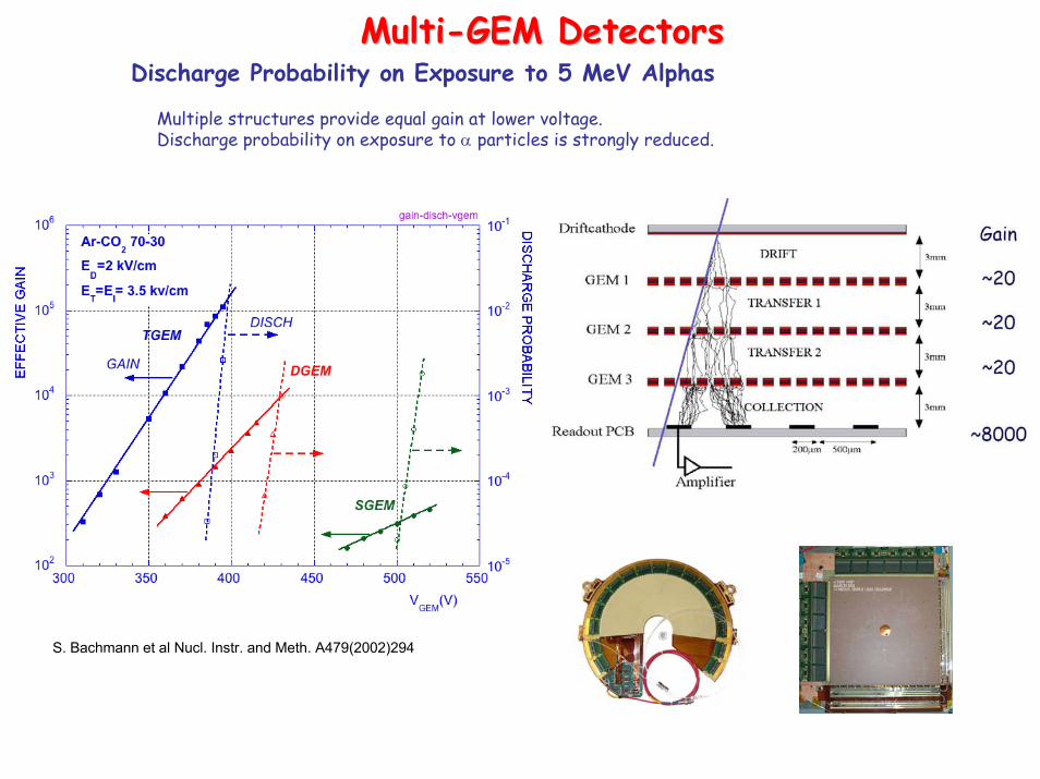
MultiMulti--GEM DetectorsGEM DetectorsDischarge Probability on Exposure to 5 MeV Alphas
Multiple structures provide equal gain at lower voltage.Discharge probability on exposure to α particles is strongly reduced.
S. Bachmann et al Nucl. Instr. and Meth. A479(2002)294
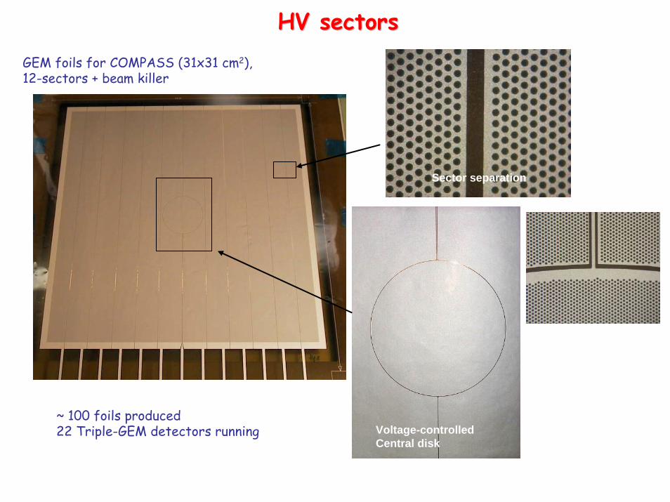
GEM foils for COMPASS (31x31 cm2), 12-sectors + beam killer
~ 100 foils produced22 Triple-GEM detectors running
Sector separation
Voltage-controlled Central disk
HV sectorsHV sectors
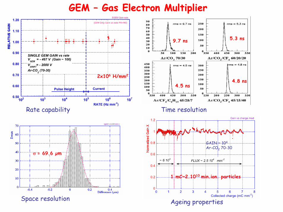
GEM GEM –– Gas Electron MultiplierGas Electron Multiplier
σ = 69.6 µm
4.5 ns4.8 ns
5.3 ns9.7 ns
Rate capability
Space resolution
Time resolution
GAIN ~ 104
Ar-CO2 70-30
1 mC~2.1010 min.ion. particles
Ageing properties
2x10⁶ H/mm2
APV with protection
Test termination card
u (mm)-150 -100 -50 0 50 100 150
0.7
0.75
0.8
0.85
0.9
0.95
1
GM06UEfficiency
128 channels
GEM GEM –– Gas Electron MultiplierGas Electron Multiplier
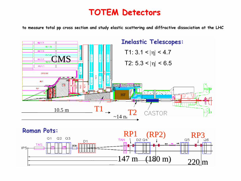
TOTEM DetectorsTOTEM Detectors
RP1RP1 (RP2)(RP2) RP3RP3
220 m220 m(180 m)(180 m)147 m147 m
Roman Pots:Roman Pots:
~14 m
CMSCMST1: 3.1 < |η| < 4.7
T2: 5.3 < |η| < 6.5
10.5 m T1T1 T2T2
HF
Inelastic Telescopes:Inelastic Telescopes:
to measure total pp cross section and study elastic scattering and diffractive dissociation at the LHC
T2 GEMT2 GEMCASTORCASTOR
TableTable
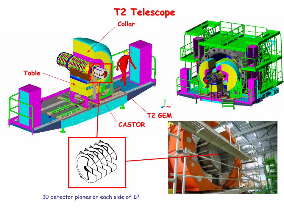
CollarCollarT2 TelescopeT2 Telescope
10 detector planes on each side of IP
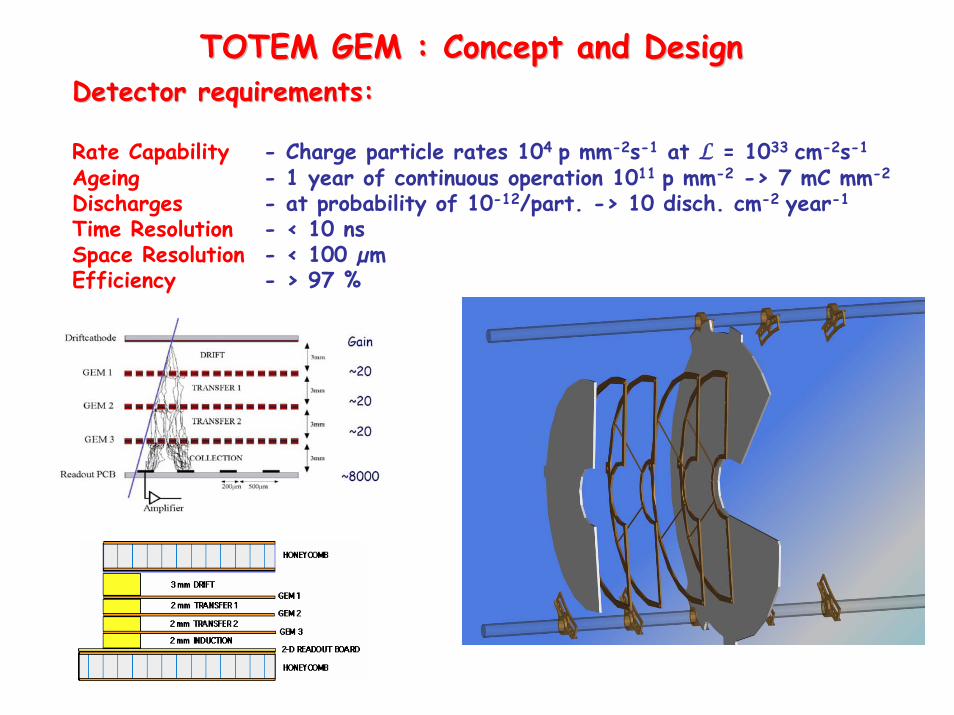
TOTEM GEM : Concept and DesignTOTEM GEM : Concept and DesignDetector requirements:Detector requirements:
Rate Capability - Charge particle rates 104 p mm-2s-1 at L = 1033 cm-2s-1
Ageing - 1 year of continuous operation 1011 p mm-2 -> 7 mC mm-2
Discharges - at probability of 10-12/part. -> 10 disch. cm-2 year-1
Time Resolution - < 10 nsSpace Resolution - < 100 µmEfficiency - > 97 %
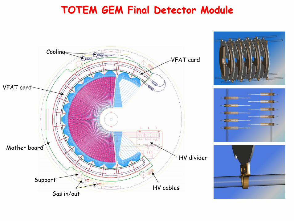
TOTEM GEM Final Detector ModuleTOTEM GEM Final Detector Module
Gas in/outHV cables
HV divider
Cooling
Support
Mother board
VFAT card
VFAT card
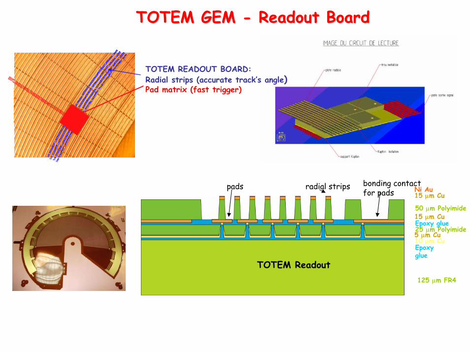
TOTEM READOUT BOARD:Radial strips (accurate track’s angle)Pad matrix (fast trigger)
TOTEM GEM TOTEM GEM -- Readout BoardReadout Board
50 μm Polyimide
25 μm Polyimide
125 μm FR4
15 μm CuEpoxy glue
5 μm Cu10 μm CuEpoxy glue
Ni Au15 μm Cu
TOTEM Readout
radial stripspads bonding contactfor pads
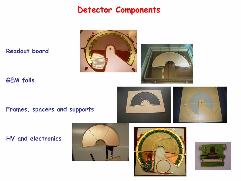
Readout board
GEM foils
Frames, spacers and supports
HV and electronics
Detector ComponentsDetector Components
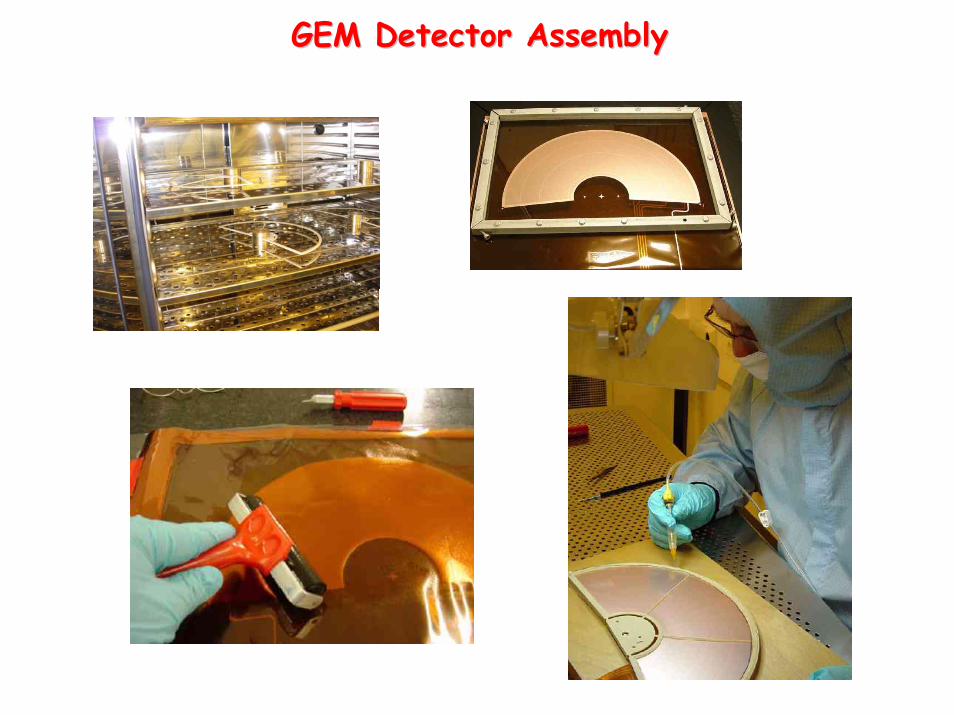
GEM Detector AssemblyGEM Detector Assembly
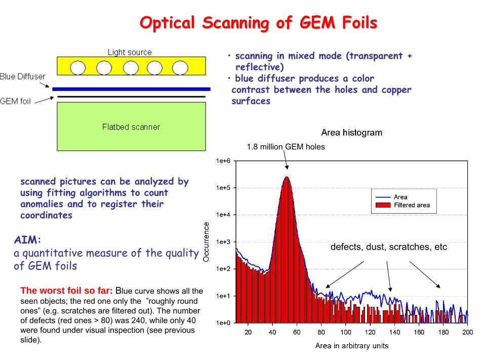
Optical Scanning of GEM FoilsOptical Scanning of GEM Foils
• scanning in mixed mode (transparent + reflective)
• blue diffuser produces a color contrast between the holes and copper surfaces
1.8 million GEM holes
defects, dust, scratches, etc
scanned pictures can be analyzed by using fitting algorithms to count anomalies and to register their coordinates
The worst foil so far: Blue curve shows all the seen objects; the red one only the ”roughly round ones” (e.g. scratches are filtered out). The number of defects (red ones > 80) was 240, while only 40 were found under visual inspection (see previous slide).
AIM:a quantitative measure of the quality of GEM foils
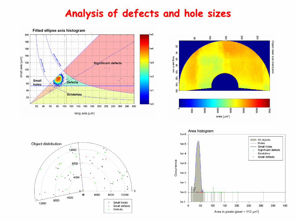
Analysis of defects and hole sizesAnalysis of defects and hole sizes
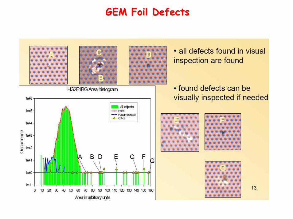
GEM Foil DefectsGEM Foil Defects
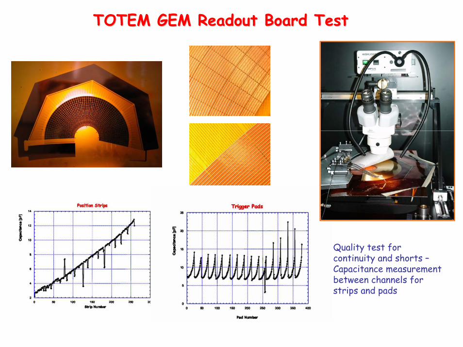
TOTEM GEM Readout Board TestTOTEM GEM Readout Board Test
Quality test forcontinuity and shorts –Capacitance measurementbetween channels forstrips and pads
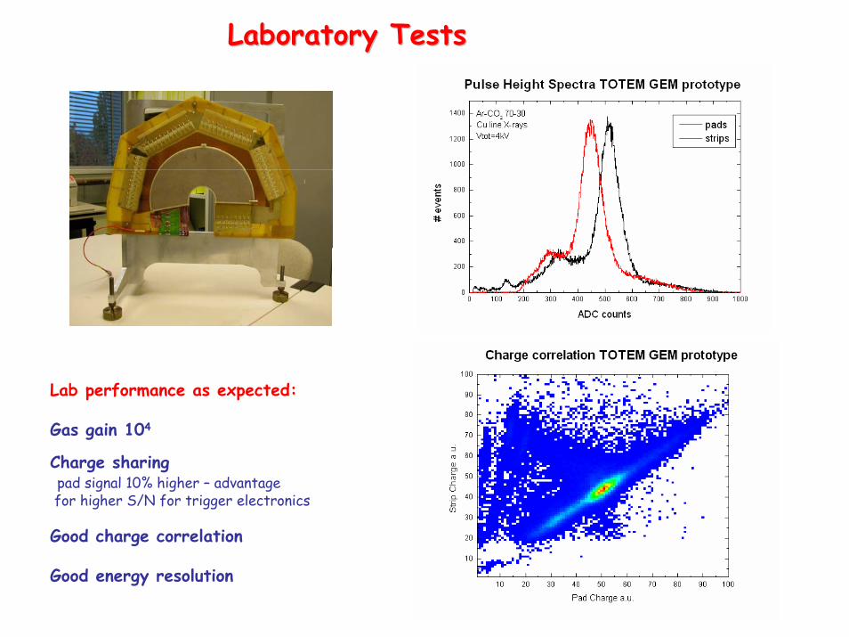
Laboratory TestsLaboratory Tests
Lab performance as expected:
Gas gain 104
Charge sharingpad signal 10% higher – advantage for higher S/N for trigger electronics
Good charge correlation
Good energy resolution
0 100 200 300 400 500 600 700
0
100
200
300
400
500
StripAmpVsStrip_Proj01_Smpl02
Entries 5194Mean x 370.9Mean y 24.52RMS x 221.2RMS y 11.31
StripAmpVsStrip_Proj01_Smpl02
Entries 5194Mean x 370.9Mean y 24.52RMS x 221.2RMS y 11.31
GM01 Strip amplitude projection vs strip
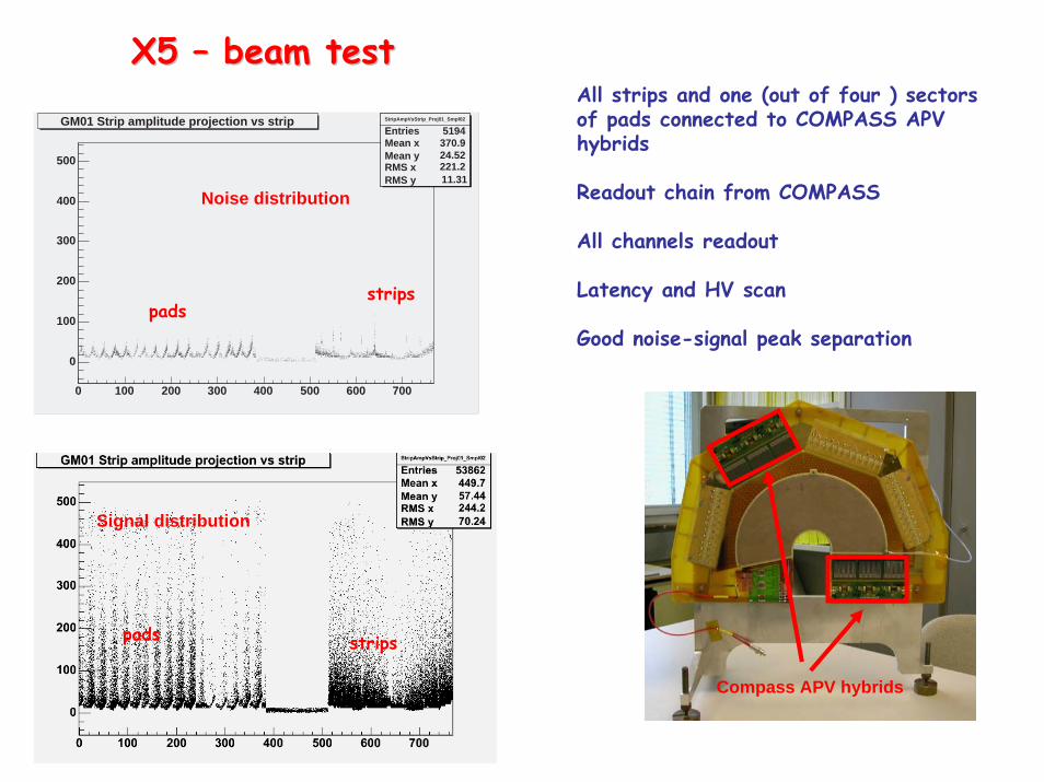
X5 X5 –– beam testbeam test
padsstrips
Noise distribution
Compass APV hybrids
All strips and one (out of four ) sectors of pads connected to COMPASS APV hybrids
Readout chain from COMPASS
All channels readout
Latency and HV scan
Good noise-signal peak separation
pads strips
Signal distribution
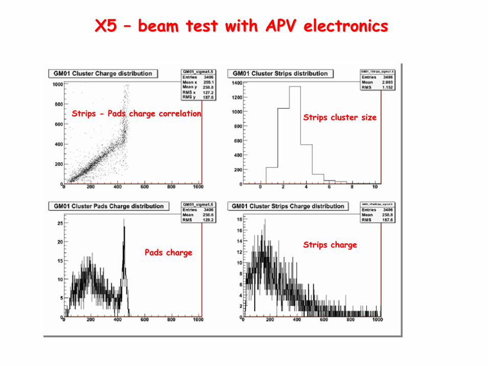
X5 X5 –– beam test with APV electronicsbeam test with APV electronics
Pads chargePads chargeStrips chargeStrips charge
Strips cluster size Strips cluster size Strips Strips -- Pads charge correlationPads charge correlation
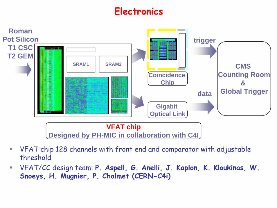
VFAT chip 128 channels with front end and comparator with adjustable thresholdVFAT/CC design team: P. Aspell, G. Anelli, J. Kaplon, K. Kloukinas, W. Snoeys, H. Mugnier, P. Chalmet (CERN-C4i)
ElectronicsElectronics
VFAT chipDesigned by PH-MIC in collaboration with C4I
Roman Pot Silicon
T1 CSCT2 GEM
trigger
Coincidence Chip
CMS Counting Room
& Global Trigger
Gigabit Optical Link
data
SRAM1 SRAM2
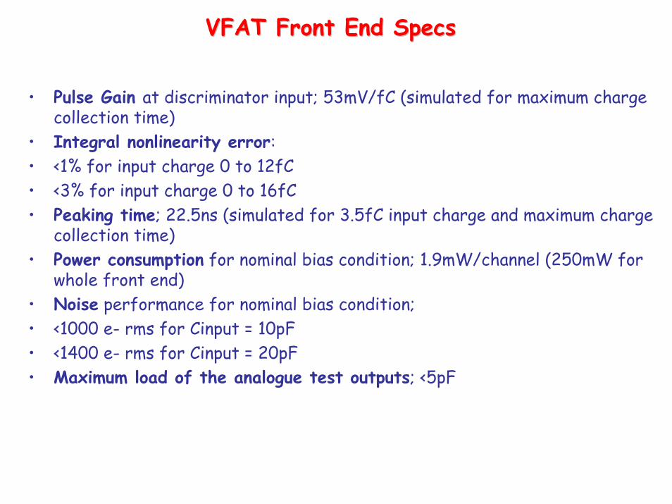
VFAT Front End SpecsVFAT Front End Specs
• Pulse Gain at discriminator input; 53mV/fC (simulated for maximum charge collection time)
• Integral nonlinearity error: • <1% for input charge 0 to 12fC• <3% for input charge 0 to 16fC• Peaking time; 22.5ns (simulated for 3.5fC input charge and maximum charge
collection time)• Power consumption for nominal bias condition; 1.9mW/channel (250mW for
whole front end)• Noise performance for nominal bias condition;• <1000 e- rms for Cinput = 10pF• <1400 e- rms for Cinput = 20pF• Maximum load of the analogue test outputs; <5pF
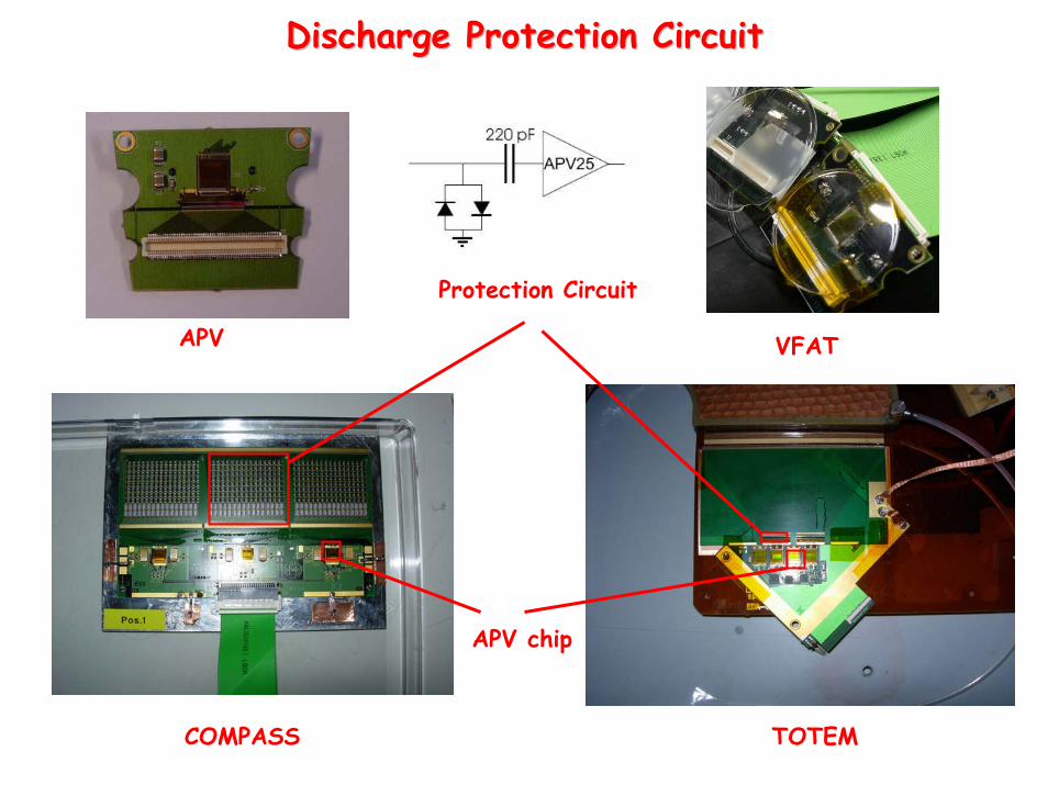
APV chip
COMPASS TOTEM
Protection Circuit
Discharge Protection CircuitDischarge Protection Circuit
APV VFAT
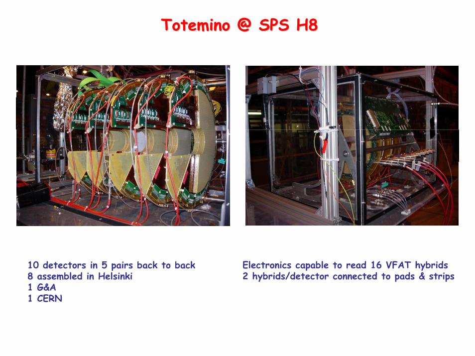
Totemino @ SPS H8Totemino @ SPS H8
10 detectors in 5 pairs back to back8 assembled in Helsinki1 G&A1 CERN
Electronics capable to read 16 VFAT hybrids2 hybrids/detector connected to pads & strips
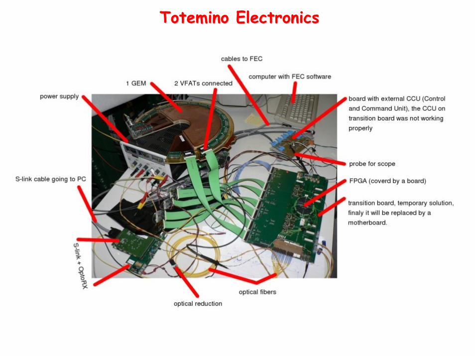
Totemino ElectronicsTotemino Electronics
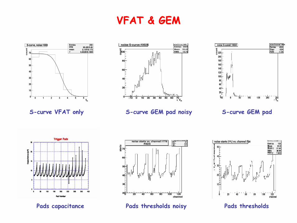
VFAT & GEMVFAT & GEM
S-curve VFAT only S-curve GEM pad noisy S-curve GEM pad
Pads capacitance Pads thresholds noisy Pads thresholds
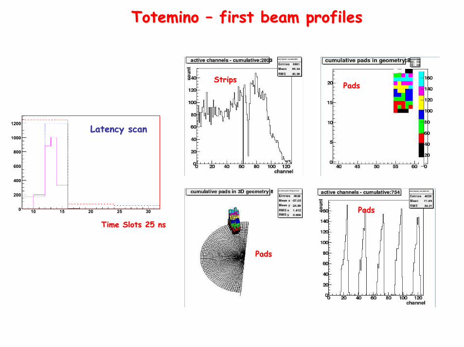
Totemino Totemino –– first beam profilesfirst beam profiles
StripsStripsPadsPads
PadsPads
PadsPads
Latency scanLatency scan
Time Slots 25 nsTime Slots 25 ns
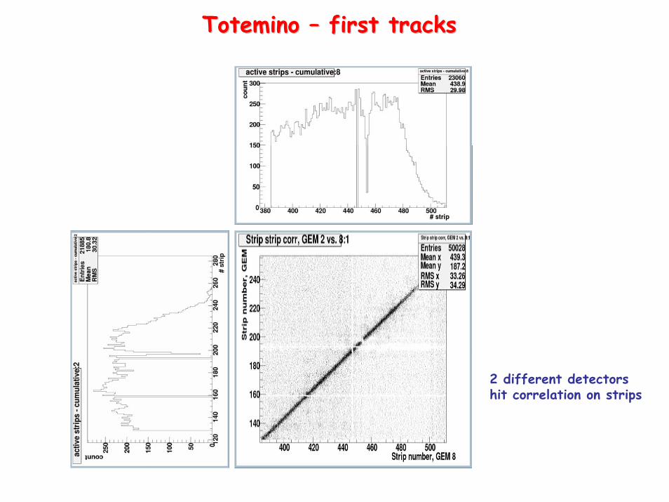
Totemino Totemino –– first tracksfirst tracks
2 different detectorshit correlation on strips
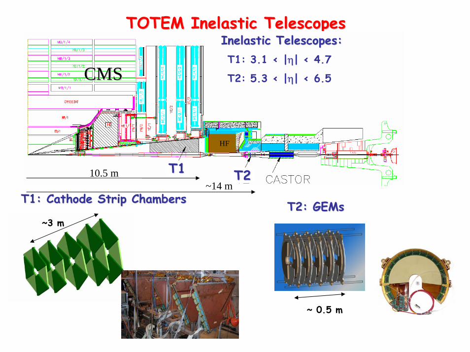
TOTEM Inelastic TelescopesTOTEM Inelastic Telescopes
~3 m
T1: Cathode Strip ChambersT1: Cathode Strip Chambers~14 m
CMSCMST1: 3.1 < |η| < 4.7
T2: 5.3 < |η| < 6.5
10.5 m T1T1 T2T2
HF
Inelastic Telescopes:Inelastic Telescopes:
T2: GEMsT2: GEMs
~ 0.5 m
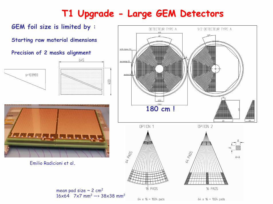
T1 Upgrade T1 Upgrade -- Large GEM DetectorsLarge GEM DetectorsGEM foil size is limited by :
Starting raw material dimensions
Precision of 2 masks alignment
mean pad size ~ 2 cm2
16x64 7x7 mm2 —› 38x38 mm2
180 cm !
Emilio Radicioni et al.
50 μm Kapton5 μm Cu both sides
Photoresist coating, masking and exposureto UV light
Metal etching
Kapton etching
Second masking
Metal etching and cleaning
GEM ManufacturingGEM Manufacturing
Double mask process
Single mask process
Positively tested for:
Gas gainCharging up process (asymmetry)Maximum gain in presence of HIPs
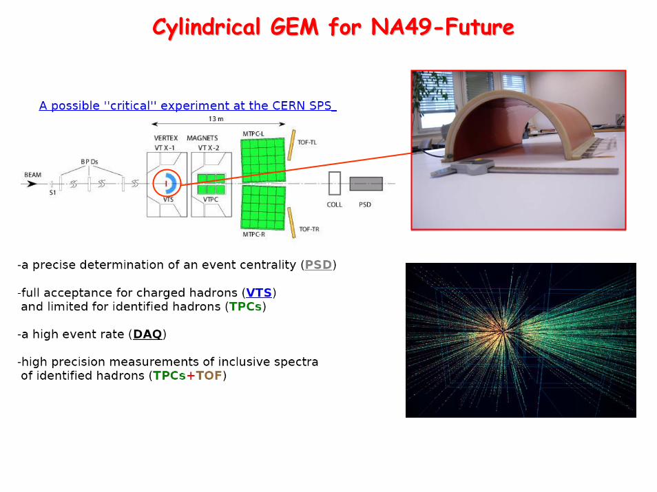
Cylindrical GEM for NA49Cylindrical GEM for NA49--FutureFuture
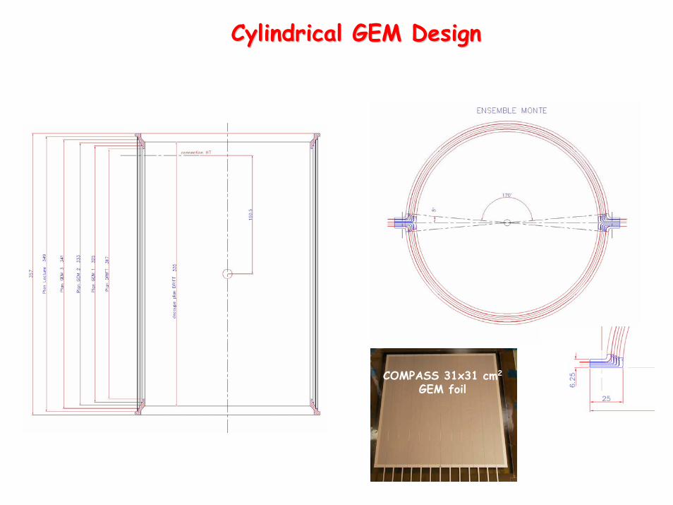
COMPASS 31x31 cm2
GEM foil
Cylindrical GEM DesignCylindrical GEM Design
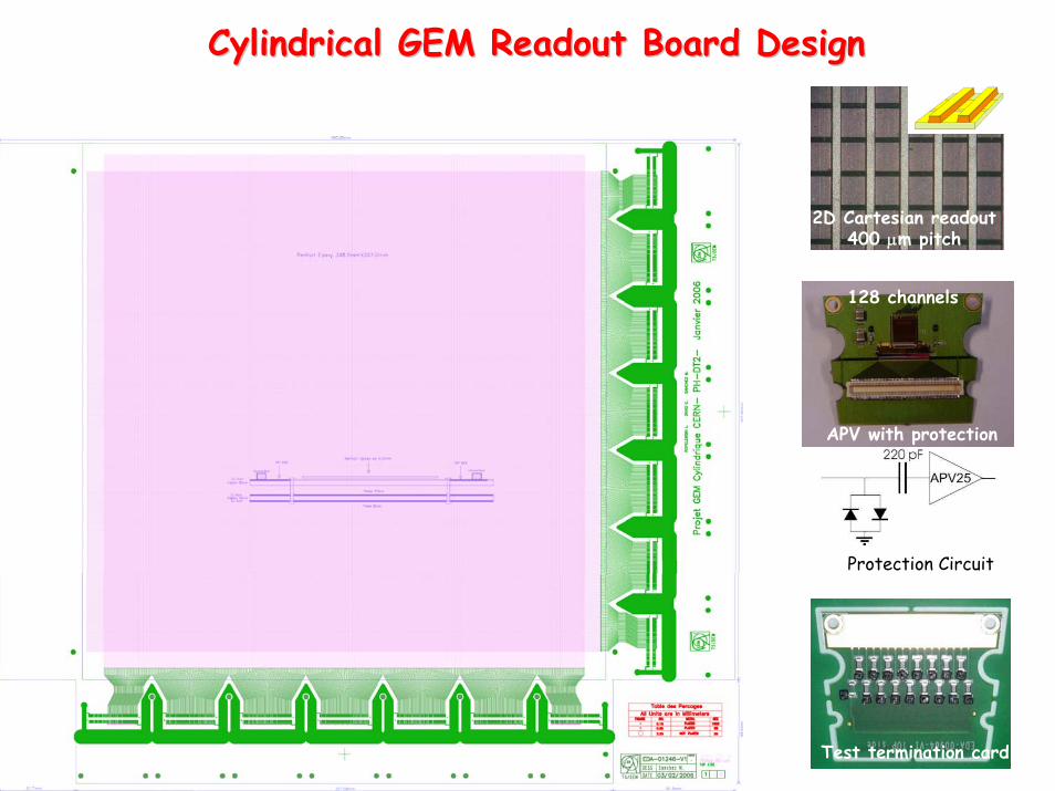
Protection Circuit
APV with protection
Test termination card
2D Cartesian readout400 μm pitch
Cylindrical GEM Readout Board DesignCylindrical GEM Readout Board Design
128 channels
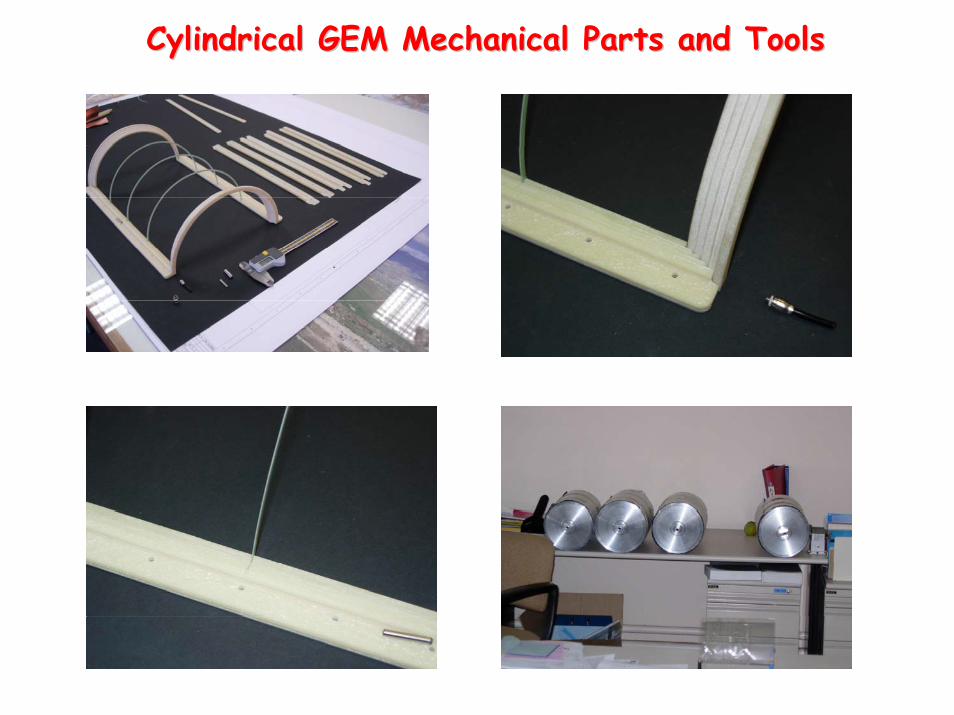
Cylindrical GEM Mechanical Parts and ToolsCylindrical GEM Mechanical Parts and Tools
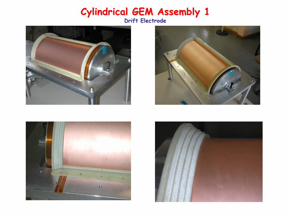
Cylindrical GEM Assembly 1Cylindrical GEM Assembly 1Drift ElectrodeDrift Electrode
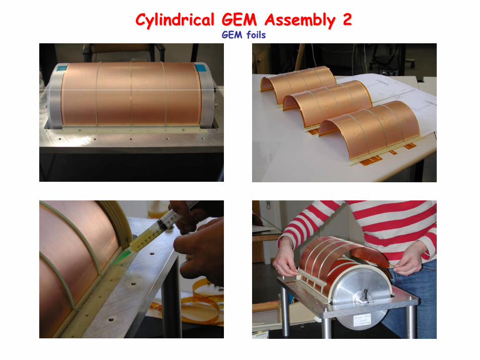
Cylindrical GEM Assembly 2Cylindrical GEM Assembly 2GEM foilsGEM foils
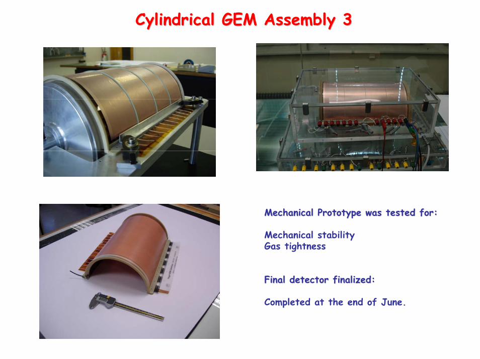
Cylindrical GEM Assembly 3Cylindrical GEM Assembly 3
Mechanical Prototype was tested for:Mechanical Prototype was tested for:
Mechanical stabilityGas tightness
Final detector finalized:Final detector finalized:
Completed at the end of June.
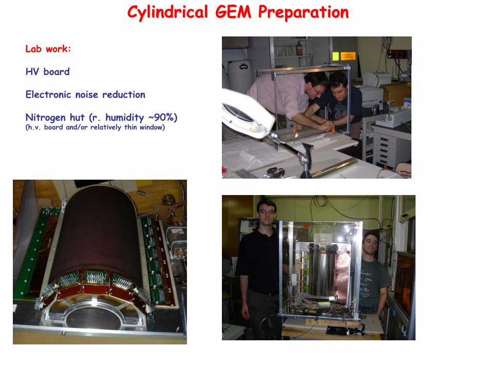
Cylindrical GEM PreparationCylindrical GEM Preparation
Lab work:
HV board
Electronic noise reduction
Nitrogen hut (r. humidity ~90%)(h.v. board and/or relatively thin window)
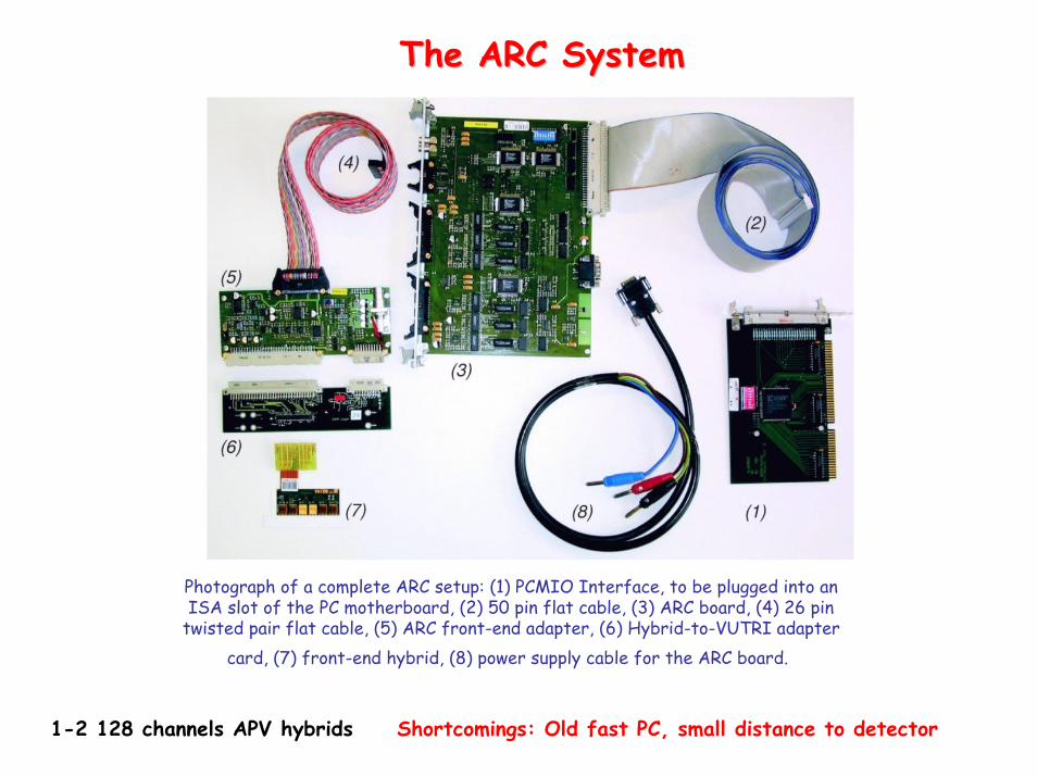
Photograph of a complete ARC setup: (1) PCMIO Interface, to be plugged into anISA slot of the PC motherboard, (2) 50 pin flat cable, (3) ARC board, (4) 26 pin
twisted pair flat cable, (5) ARC front-end adapter, (6) Hybrid-to-VUTRI adaptercard, (7) front-end hybrid, (8) power supply cable for the ARC board.
The ARC SystemThe ARC System
1-2 128 channels APV hybrids Shortcomings: Old fast PC, small distance to detector
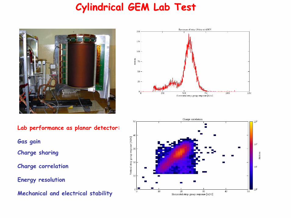
Cylindrical GEM Lab TestCylindrical GEM Lab Test
Lab performance as planar detector:
Gas gain
Charge sharing
Charge correlation
Energy resolution
Mechanical and electrical stability
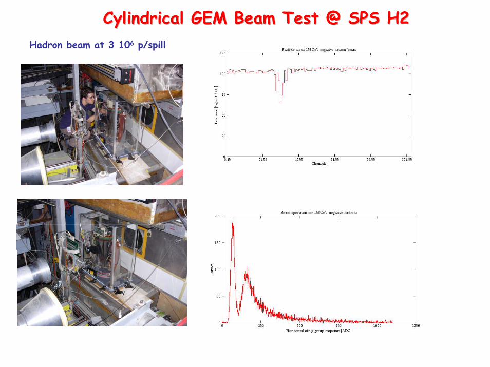
Cylindrical GEM Beam Test @ SPS H2Cylindrical GEM Beam Test @ SPS H2Hadron beam at 3 106 p/spill
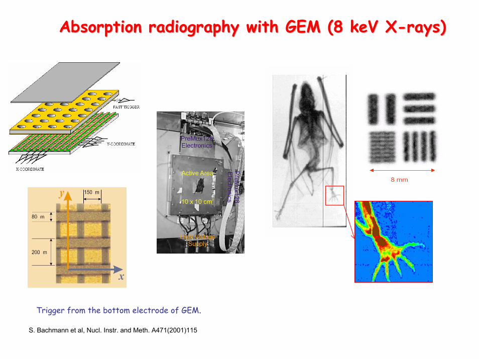
Absorption radiography with GEM (8 keV XAbsorption radiography with GEM (8 keV X--rays)rays)
Trigger from the bottom electrode of GEM.
S. Bachmann et al, Nucl. Instr. and Meth. A471(2001)115
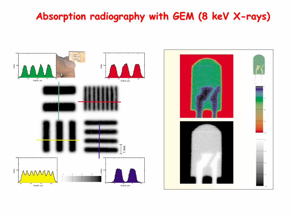
Absorption radiography with GEM (8 keV XAbsorption radiography with GEM (8 keV X--rays)rays)
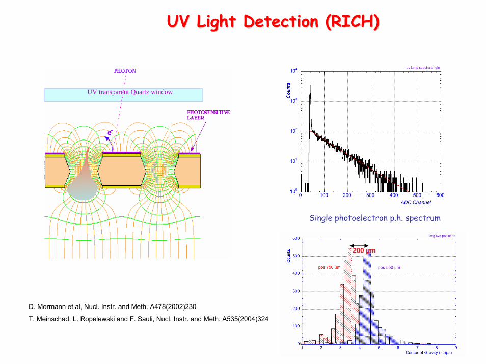
UV Light Detection (RICH)UV Light Detection (RICH)
UV transparent Quartz window
200 µm
D. Mormann et al, Nucl. Instr. and Meth. A478(2002)230
T. Meinschad, L. Ropelewski and F. Sauli, Nucl. Instr. and Meth. A535(2004)324
Single photoelectron p.h. spectrum
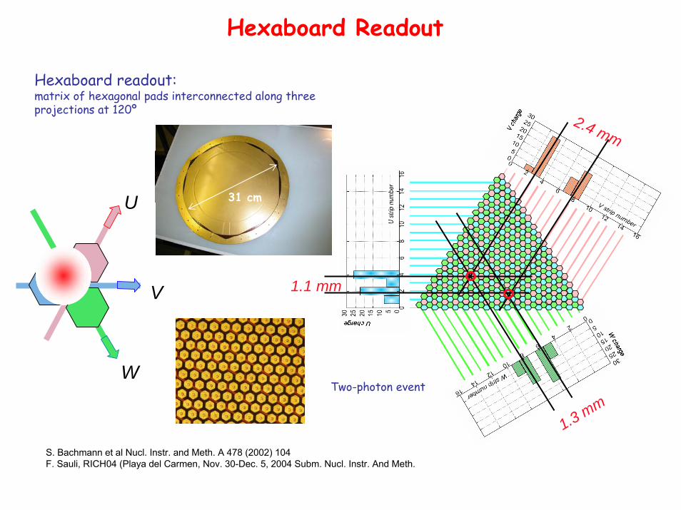
Hexaboard readout:matrix of hexagonal pads interconnected along three projections at 120º
U
V
W
S. Bachmann et al Nucl. Instr. and Meth. A 478 (2002) 104F. Sauli, RICH04 (Playa del Carmen, Nov. 30-Dec. 5, 2004 Subm. Nucl. Instr. And Meth.
1.1 mm
2.4 mm
1.3 mm
Hexaboard Readout
Two-photon event
31 cm
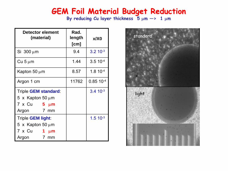
GEM Foil Material Budget ReductionGEM Foil Material Budget ReductionBy reducing Cu layer thickness 5 By reducing Cu layer thickness 5 μμm m ――> 1 > 1 μμmm
Detector element (material)
Rad. length [cm]
x/X0
Si 300 μm 9.4 3.2 10-3
Cu 5 μm 1.44 3.5 10-4
Kapton 50 μm 8.57 1.8 10-4
Argon 1 cm 11762 0.85 10-4
Triple GEM standard:5 x Kapton 50 μm7 x Cu 5 μmArgon 7 mm
3.4 10-3
Triple GEM light:5 x Kapton 50 μm7 x Cu 1 μmArgon 7 mm
1.5 10-3
standard
light
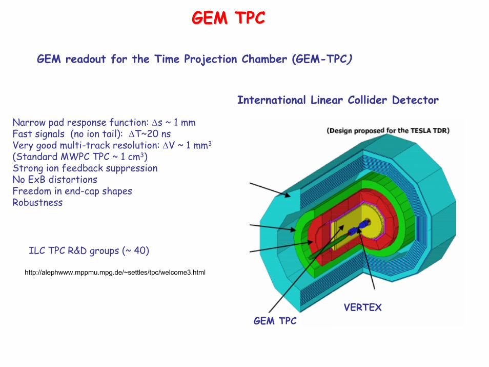
GEM TPCGEM TPC
GEM TPCVERTEX
GEM readout for the Time Projection Chamber (GEM-TPC)
International Linear Collider Detector
ILC TPC R&D groups (~ 40)
http://alephwww.mppmu.mpg.de/~settles/tpc/welcome3.html
Narrow pad response function: Δs ~ 1 mmFast signals (no ion tail): ΔT~20 nsVery good multi-track resolution: ΔV ~ 1 mm3
(Standard MWPC TPC ~ 1 cm3)Strong ion feedback suppressionNo ExB distortionsFreedom in end-cap shapesRobustness
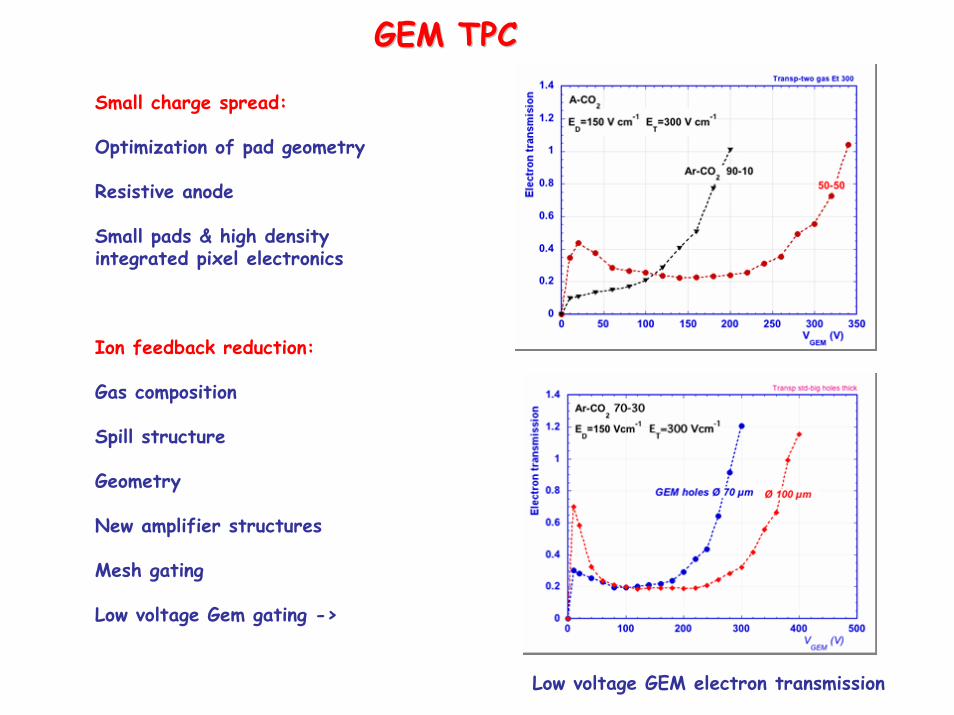
GEM TPCGEM TPC
Small charge spread:
Optimization of pad geometry
Resistive anode
Small pads & high densityintegrated pixel electronics
Ion feedback reduction:
Gas composition
Spill structure
Geometry
New amplifier structures
Mesh gating
Low voltage Gem gating ->
Low voltage GEM electron transmission
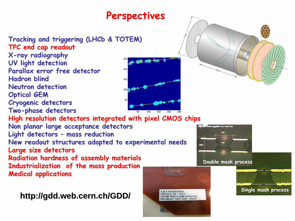
PerspectivesPerspectives
Tracking and triggering (LHCb & TOTEM)Tracking and triggering (LHCb & TOTEM)TPC end cap readoutTPC end cap readoutXX--ray radiographyray radiographyUV light detectionUV light detectionParallax error free detectorParallax error free detectorHadron blindHadron blindNeutron detectionNeutron detectionOptical GEMOptical GEMCryogenic detectorsCryogenic detectorsTwoTwo--phase detectorsphase detectorsHigh resolution detectors integrated with pixel CMOS chipsHigh resolution detectors integrated with pixel CMOS chipsNon planar large acceptance detectorsNon planar large acceptance detectorsLight detectors Light detectors –– mass reductionmass reductionNew readout structures adopted to experimental needsNew readout structures adopted to experimental needsLarge size detectorsLarge size detectorsRadiation hardness of assembly materialsRadiation hardness of assembly materialsIndustrialization of the mass productionIndustrialization of the mass productionMedical applicationsMedical applications
Single mask process
Double mask process
http://gdd.web.cern.ch/GDD/http://gdd.web.cern.ch/GDD/
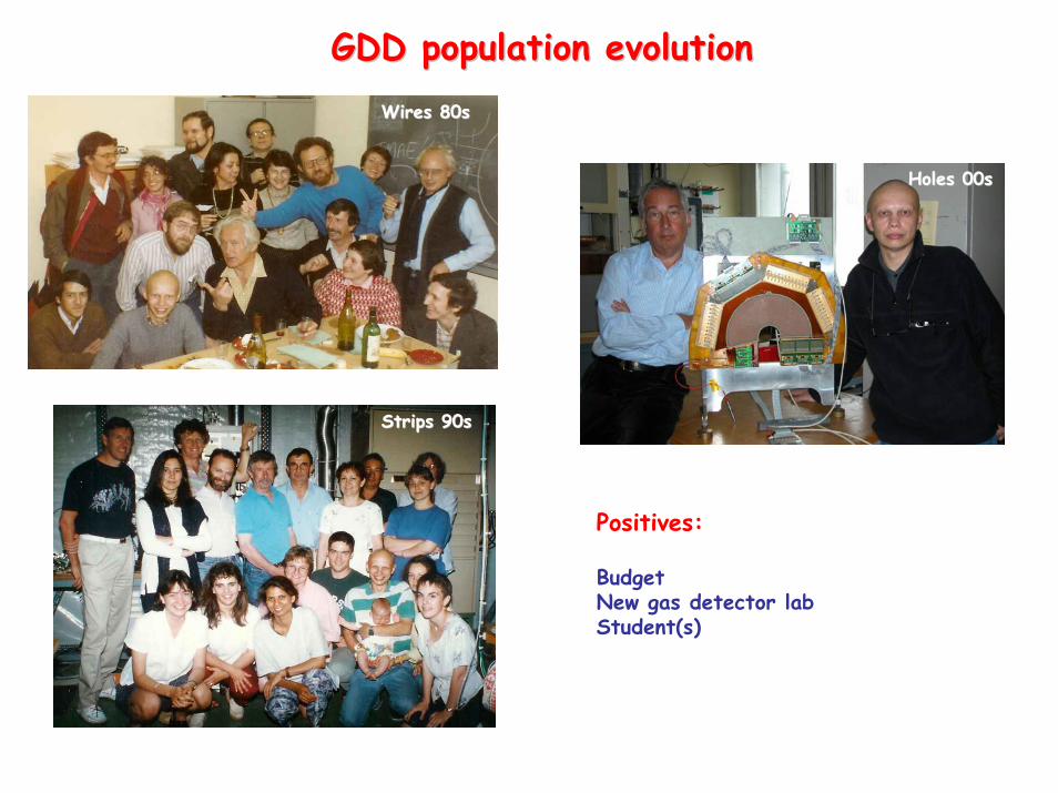
GDD population evolutionGDD population evolutionWires 80sWires 80s
Strips 90sStrips 90s
Holes 00sHoles 00s
Positives:
BudgetNew gas detector labStudent(s)
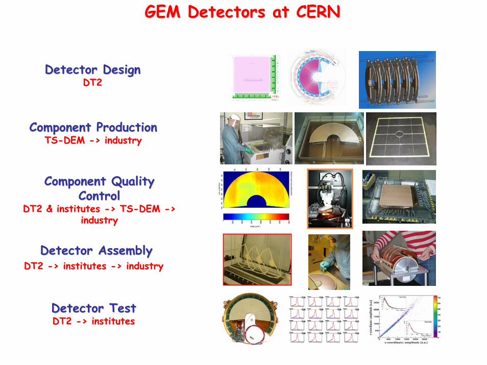
Detector DesignDetector DesignDT2DT2
Component ProductionComponent ProductionTSTS--DEM DEM --> industry> industry
Component QualityComponent QualityControlControl
DT2 & institutes DT2 & institutes --> TS> TS--DEM DEM --> > industryindustry
Detector AssemblyDetector AssemblyDT2 DT2 --> institutes > institutes --> industry> industry
Detector TestDetector TestDT2 DT2 --> institutes> institutes
GEM Detectors at CERNGEM Detectors at CERN
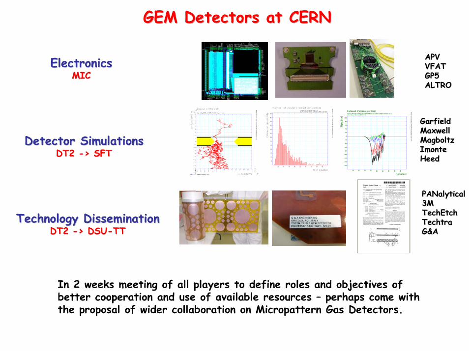
GEM Detectors at CERNGEM Detectors at CERN
ElectronicsElectronicsMICMIC
Detector SimulationsDetector SimulationsDT2 DT2 --> SFT> SFT
Technology DisseminationTechnology DisseminationDT2 DT2 --> DSU> DSU--TTTT
APVAPVVFATVFATGP5GP5ALTROALTRO
GarfieldGarfieldMaxwellMaxwellMagboltz Magboltz Imonte Imonte HeedHeed
PANalyticalPANalytical3M3MTechEtchTechEtchTechtraTechtraG&AG&A
In 2 weeks meeting of all players to define roles and objectives ofbetter cooperation and use of available resources – perhaps come withthe proposal of wider collaboration on Micropattern Gas Detectors.