Embed Size (px)
Citation preview
© 2012 WILEY-VCH Verlag GmbH & Co. KGaA, Weinheim 1
www.advmat.dewww.MaterialsViews.com
wileyonlinelibrary.com
COM
MUN
ICATIO
N
Woong Choi , Mi Yeon Cho , Aniruddha Konar , Jong Hak Lee , Gi-Beom Cha , Soon Cheol Hong , Sangsig Kim , Jeongyong Kim , Debdeep Jena , Jinsoo Joo , * and Sunkook Kim *
High-Detectivity Multilayer MoS 2 Phototransistors with Spectral Response from Ultraviolet to Infrared
Dr. J. H. Lee, Prof. S. KimDepartment of Electronics and Radio EngineeringInstitute for Laser EngineeringKyung Hee UniversityGyeonggi, 446-701, South KoreaE-mail: [email protected] Prof. W. ChoiSchool of Advanced Materials EngineeringKookmin UniversitySeoul 136-702, South Korea Dr. M. Y. Cho, Prof. J. Joo Department of PhysicsKorea UniversitySeoul 136-713, South KoreaE-mail: [email protected] Dr. A. Konar, Prof. D. JenaDepartment of Electrical EngineeringUniversity of Notre DameNotre Dame, Indiana 46556, USA Dr. G.-B. Cha, Prof. S. C. HongDepartment of Physics and Energy Harvest-Storage Research CenterUniversity of UlsanUlsan 680-749, South Korea Prof. J. KimDepartment of PhysicsUniversity of IncheonIncheon 406-772, South Korea Prof. S. KimSchool of Electrical EngineeringKorea UniversitySeoul 136-713, South Korea
DOI: 10.1002/adma.201201909
Recently, one of the transition metal dichalcogenides MoS 2 has generated substantial interest as a promising channel mate-rial for fi eld-effect transistors (FETs), because of its intriguing electrical [ 1 , 2 ] and optical properties. [ 3 ] For example, FETs using single layer MoS 2 exhibited a high current ON/OFF ratio ( ! 10 8 ) and a low subthreshold swing (SS, ! 70 mV decade " 1 ) with an electron mobility of ! 200 cm 2 V " 1 s " 1 in an HfO 2 /MoS 2 /SiO 2 dielectric environment. [ 1 ] In addition, single layer MoS 2 tran-sistors exhibited a higher photoresponsivity (7.5 mAW " 1 ) than graphene FETs, presenting a potential application as a photo transistor. [ 3 ] Yet, the fabrication demands and the physics of MoS 2 , among other reasons, suggest that multilayer MoS 2 may be more attractive than single layer MoS 2 for FET applications in a thin-fi lm transistor (TFT) confi guration. [ 4 ] For example, the synthesis of single layer MoS 2 followed by the deposition of an additional high- k dielectric layer may not be well-suited for commercial fabrication processes. In addition, the density
of states in multilayer MoS 2 is three times higher than in single layer MoS 2 , which can produce considerably high drive cur-rents in the ballistic limit. [ 5 ] In long-channel TFTs, multiple conducting channels can be created by fi eld-effects in multi-layer MoS 2, which can boost the current drive of TFTs, similar to silicon-on-insulator MOSFETs. Moreover, multilayer MoS 2 offers a wider spectral response than single layer MoS 2 " from ultraviolet (UV) to near infrared (NIR) wavelengths " due to its narrower bandgap, which can be advantageous in a variety of photodetector applications. [ 6 ] However, multilayer MoS 2 and the corresponding dichalcogenide semiconductors have not been extensively studied for use in electronics or optoelectronics. [ 7 , 8 ] The characteristics in the few early reports [ 9 , 10 ] are not particu-larly competitive with current TFT technologies.
Therefore, in this work, we further explore the optoelec-tronic properties of multilayer MoS 2 TFTs and show a compel-ling case of multilayer MoS 2 phototransistors for applications in photodetectors. In particular, the interesting optoelectronic properties of our multilayer MoS 2 phototransistors could potentially lead to their integration into touch screen panels for fl at panel or fl exible display devices. Since the presence of external millimeter-scale touch-detecting devices (e.g., using capacitive or resistive touch sensors) in touch screen panels sig-nifi cantly degrades the image quality and brightness of these display devices, integration of sub-micrometer phototransis-tors into touch screen panels has been suggested as a way of minimizing the degradation. [ 11 ] While several semiconductors, including amorphous InGaZnO, have been reported for uses as phototransistors in touch screen panels, [ 12 ] problems, such as high power consumption and reliability, remain due to their high gate bias ( > 10 V), high SS ( > 100 mV decade " 1 ) and notable shift (a few V) in the threshold voltage during illumination. In contrast, our multilayer MoS 2 phototransistors with an atomic-layer-deposited (ALD) Al 2 O 3 gate dielectric layer in a bottom gate TFT confi guration achieve high room temperature mobili-ties ( > 70 cm 2 V " 1 s " 1 ), a low operating gate bias ( < 5 V), and a negligible shift in the threshold voltages during illumination. Furthermore, our multilayer MoS 2 phototransistors exhibit better optoelectronic properties than single layer MoS 2 photo-transistors, including a wider spectral response ( < ! 900 nm) and higher photoresponsivity ( > 100 mAW " 1 ).
Before fabricating the MoS 2 phototransistors, we fi rst meas-ured the optical absorption in multilayer MoS 2 fl akes with dif-ferent thicknesses across the visible and near-infrared (NIR) spectral ranges ( Figure 1 (a)). The thicknesses of MoS 2 fl akes measured by a tapping mode atomic force microscopy (AFM) are ! 40 nm, ! 4 nm, and ! 1 nm, in sequence. Regardless of their thicknesses, all of the MoS 2 fl akes show two excitonic
Adv. Mater. 2012, DOI: 10.1002/adma.201201909
2
www.advmat.dewww.MaterialsViews.com
wileyonlinelibrary.com © 2012 WILEY-VCH Verlag GmbH & Co. KGaA, Weinheim
COM
MUN
ICATI
ON
absorption peaks " ‘A’ and ‘B’ " between 600 nm and 700 nm arising from the K point of the Brillouin zone. [ 13 , 14 ] Their energy differences are due to the spin-orbital splitting of the valence band, as indicated in Figure 1 (b). For the thick MoS 2 fl ake (40 nm), an optical absorption tail " labeled ‘I’ " is observed
through the indirect band transition at a wavelength longer than ! 700 nm. However, as the thickness of MoS 2 fl akes approached 1 nm, this absorption tail becomes weaker. This observation is consistent with the fact that single layer MoS 2 is a direct band gap semiconductor where the lowest energy interband transition occurs at the K point of the Brillouin zone. [ 13 , 14 ]
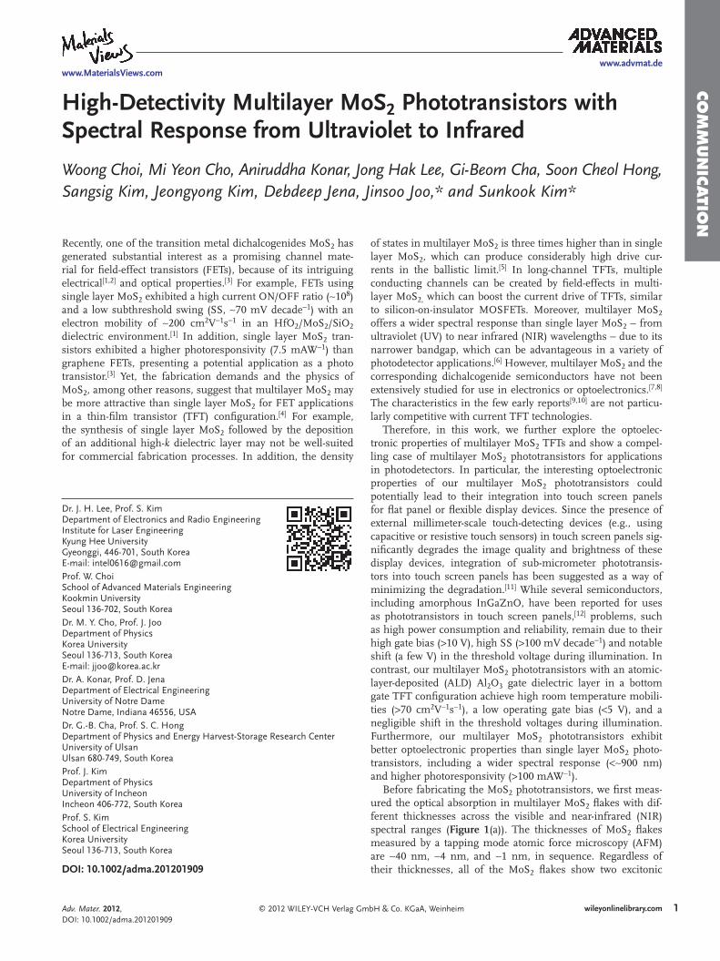
Next, multilayer MoS 2 TFTs are fabricated as shown in Figure 2 (a) and their electrical transport properties are measured in a back-gated structure at room temperature. The thicknesses of MoS 2 fl akes are in the range of 10–60 nm. Figures 2 (c)-(d) show the tran-sistor characteristics for multilayer MoS 2 TFTs (gate length ! 3 µ m, width ! 7 µ m, and thickness of MoS 2 channel ! 20 nm) with a 50-nm-thick ALD Al 2 O 3 gate insulator. The integration of high- # dielectrics allows lower power consumption than SiO 2 ( # = 3.9) due to increased gate capacitance and dielectric
screening of Coulomb scattering. [ 15 ] The measured current-voltage (I–V) behavior shows good agreement with a conven-tional long-channel NMOS transistor, exhibiting a linear triode regime at low drain voltages (V ds ) and a saturation regime at high V ds . Unlike the reported 2D-crystal-based electronics, such
as pristine graphene FETs [ 16 , 17 ] and single layer MoS 2 TFTs, [ 3 ] our transistors exhibit a current saturation at high V ds . Saturation current at the “pinched-off” condition is independent of V ds and is operated by the gate voltage according to the CMOS square-law model, in which the high output resist-ance in the saturation regime is a key factor to achieve a high voltage gain and to isolate output from the input signal in digital cir-cuits. The representative multilayer MoS 2 TFT exhibits a maximum transconductance (g m = dI d /dV gs | Vds = 0.2V ) of 3.12 µ S, and an I on /I off of ! 1 $ 10 6 . Note that the leakage cur-rent through the back gate in the operating regime is lower than the drain current by at least eight orders of magnitude. Based on the standard model of metal-oxide-semicon-ductor fi eld-effect transistors (MOSFETs) and a parallel plate model of gate capaci-tance, the fi eld effect mobility ( µ eff = Lg m /(WC ox V ds )) extracted from our experimental transfer curves is > 70 cm 2 V " 1 s " 1 in the linear regime (V ds = 0.2 V). Interestingly, our mul-tilayer MoS 2 transistors provide a higher µ eff than those reported in conventional TFTs that are based on amorphous Si, low temperature poly-Si, or amorphous oxide semiconductors. [ 12 ]
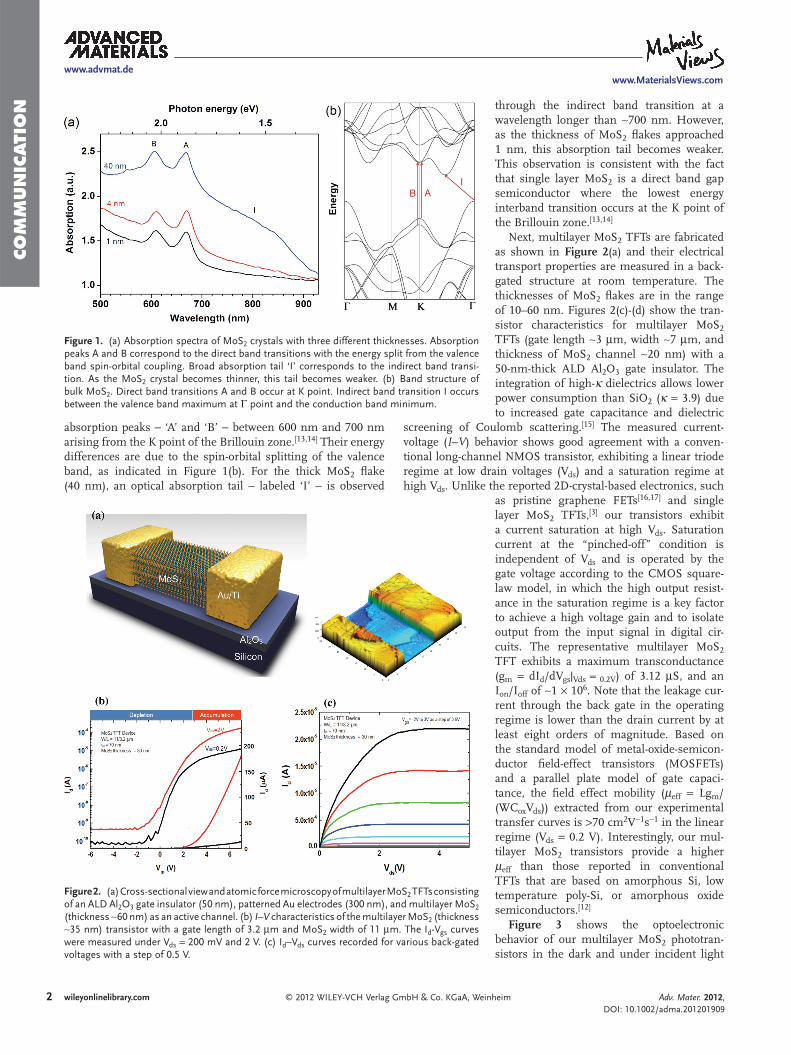
Figure 3 shows the optoelectronic behavior of our multilayer MoS 2 phototran-sistors in the dark and under incident light
Figure 1 . (a) Absorption spectra of MoS 2 crystals with three different thicknesses. Absorption peaks A and B correspond to the direct band transitions with the energy split from the valence band spin-orbital coupling. Broad absorption tail ‘I’ corresponds to the indirect band transi-tion. As the MoS 2 crystal becomes thinner, this tail becomes weaker. (b) Band structure of bulk MoS 2 . Direct band transitions A and B occur at K point. Indirect band transition I occurs between the valence band maximum at % point and the conduction band minimum.
Figure 2 . (a) Cross-sectional view and atomic force microscopy of multilayer MoS 2 TFTs consisting of an ALD Al 2 O 3 gate insulator (50 nm), patterned Au electrodes (300 nm), and multilayer MoS 2 (thickness ! 60 nm) as an active channel. (b) I–V characteristics of the multilayer MoS 2 (thickness ! 35 nm) transistor with a gate length of 3.2 µ m and MoS 2 width of 11 µ m. The I d -V gs curves were measured under V ds = 200 mV and 2 V. (c) I d –V ds curves recorded for various back-gated voltages with a step of 0.5 V.
Adv. Mater. 2012, DOI: 10.1002/adma.201201909
3
www.advmat.dewww.MaterialsViews.com
wileyonlinelibrary.com© 2012 WILEY-VCH Verlag GmbH & Co. KGaA, Weinheim
COM
MUN
ICATIO
N
light illumination shows the dominating effects of the thermionic and tunneling cur-rents, and the negligible contribution of the photogenerated current.
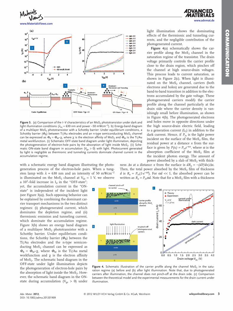
Figure 4 (a) schematically shows the car-rier profi le along the MoS 2 channel in the saturation regime of the transistor. The drain voltage primarily controls the carrier profi le close to the drain region, which pinches off the channel at high source-drain voltages. This process leads to current saturation, as shown in Figure 2 (c). When light is illumi-nated on the MoS 2 channel, carriers (both electrons and holes) are generated due to the band-to-band transition in addition to the elec-trons accumulated by the gate voltage. These photogenerated carriers modify the carrier profi le along the channel particularly at the drain side where the carrier density is van-ishingly small before illumination, as shown in Figure 4 (b). The photogenerated electrons and holes move in opposite directions under the high source-drain electric fi eld, leading to a generation current (I G ) in addition to the dark current. Hence, if P in is the light power incident on the surface of the MoS 2 fi lm, the residual power at a distance x from the sur-face is given by P(x) = P in e " & x , where & is the absorption coeffi cient of the MoS 2 fi lm at the incident photon energy. The amount of power absorbed by a slab of MoS 2 with thick-
ness ' x at a distance x from the surface is dR a = " (dP/dx) ' x . Then, the total power absorbed by the MoS 2 fi lm of thickness d is R a = P in ( 1 -e " & d ) . For & d < < 1, the absorbed power can be written as R a = P in & d. Note that for a MoS 2 fi lm with a thickness
with a schematic energy band diagram illustrating the photo-generation process of the electron-hole pairs. When a tung-sten lamp with ( = 630 nm and an intensity of 50 mWcm " 2 is illuminated on the MoS 2 channel at V ds = 1 V, we observe a 10 3 –fold increase in I d in the “OFF-state”; yet, the accumulation current in the “ON-state” is independent of the incident light (see Figure 3 (a)). Such opposing behavior can be explained by combining the dominant car-rier transport mechanisms in the two distinct regimes: (i) photogenerated current, which dominates the depletion regime, and (ii) thermionic emission and tunneling current, which dominate the accumulation regime. Figure 3 (b) shows an energy band diagram of a multilayer MoS 2 phototransistor with a Schottky barrier. Under equilibrium condi-tions, the Schottky barrier ( ) B ) between the Ti/Au electrodes and the n-type semicon-ducting MoS 2 channel can be expressed as ) B = ) M – * , where ) M is the Ti/Au metal workfunction and * is the electron affi nity of MoS 2 . The schematic band diagram in the OFF-state under light illumination depicts the photogeneration of electron-hole pairs by the absorption of light inside the MoS 2 . How-ever, the schematic band diagram in the ON-state during accumulation (V gs > 0) under
Figure 3 . (a) Comparison of the I–V characteristics of an MoS 2 phototransistor under dark and light illumination conditions ( ( ex = 630 nm and power ! 50 mWcm " 2 ). b) Energy-band diagram of a multilayer MoS 2 phototransistor with a Schottky barrier: Under equilibrium conditions, a Schottky barrier ( ) B ) between Ti/Au electrodes and an n-type semiconducting MoS 2 channel can be expressed as ) B = ) M – * , where * is the electron affi nity of MoS 2 and ) M is the Ti/Au metal workfunction. (i) Schematic OFF-state band diagram under light illumination, depicting the photogeneration of electron-hole pairs by the absorption of light inside MoS 2 . (ii) Sche-matic ON-state band diagram in accumulation (V gs > 0) with light. Photocurrent generated by light is negligible as thermionic and tunneling currents dominate channel current in the accumulation regime.
Figure 4 . Schematic illustration of the carrier profi le along the channel MoS 2 in the satu-ration regime (a) before and (b) after light illumination. Note that, due to photogenerated carriers after illumination, the channel does not pinch-off at the drain side. (c) Comparison between the theoretical model and the experimental measurements for the drain current under illumination.
Adv. Mater. 2012, DOI: 10.1002/adma.201201909
4
www.advmat.dewww.MaterialsViews.com
wileyonlinelibrary.com © 2012 WILEY-VCH Verlag GmbH & Co. KGaA, Weinheim
COM
MUN
ICATI
ON
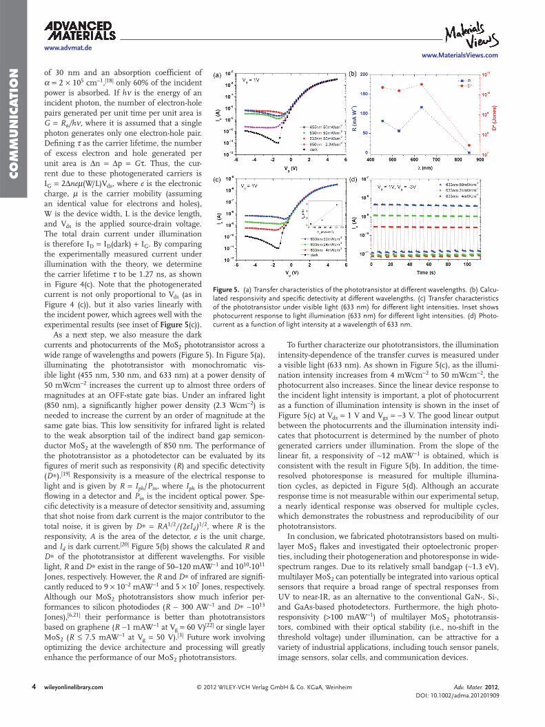
To further characterize our phototransistors, the illumination intensity-dependence of the transfer curves is measured under a visible light (633 nm). As shown in Figure 5 (c), as the illumi-nation intensity increases from 4 mWcm " 2 to 50 mWcm " 2 , the photocurrent also increases. Since the linear device response to the incident light intensity is important, a plot of photocurrent as a function of illumination intensity is shown in the inset of Figure 5 (c) at V ds = 1 V and V gs = –3 V. The good linear output between the photocurrents and the illumination intensity indi-cates that photocurrent is determined by the number of photo generated carriers under illumination. From the slope of the linear fi t, a responsivity of ! 12 mAW " 1 is obtained, which is consistent with the result in Figure 5 (b). In addition, the time-resolved photoresponse is measured for multiple illumina-tion cycles, as depicted in Figure 5 (d). Although an accurate response time is not measurable within our experimental setup, a nearly identical response was observed for multiple cycles, which demonstrates the robustness and reproducibility of our phototransistors.
In conclusion, we fabricated phototransistors based on multi-layer MoS 2 fl akes and investigated their optoelectronic proper-ties, including their photogeneration and photoresponse in wide-spectrum ranges. Due to its relatively small bandgap ( ! 1.3 eV), multilayer MoS 2 can potentially be integrated into various optical sensors that require a broad range of spectral responses from UV to near-IR, as an alternative to the conventional GaN-, Si-, and GaAs-based photodetectors. Furthermore, the high photo-responsivity ( > 100 mAW " 1 ) of multilayer MoS 2 phototransis-tors, combined with their optical stability (i.e., no-shift in the threshold voltage) under illumination, can be attractive for a variety of industrial applications, including touch sensor panels, image sensors, solar cells, and communication devices.
of 30 nm and an absorption coeffi cient of & = 2 $ 10 5 cm " 1 , [ 18 ] only 60% of the incident power is absorbed. If h + is the energy of an incident photon, the number of electron-hole pairs generated per unit time per unit area is G = R a /h + , where it is assumed that a single photon generates only one electron-hole pair. Defi ning , as the carrier lifetime, the number of excess electron and hole generated per unit area is ' n = ' p = G , . Thus, the cur-rent due to these photogenerated carriers is I G = 2 ' ne µ (W/L)V ds , where e is the electronic charge, µ is the carrier mobility (assuming an identical value for electrons and holes), W is the device width, L is the device length, and V ds is the applied source-drain voltage. The total drain current under illumination is therefore I D = I D (dark) + I G . By comparing the experimentally measured current under illumination with the theory, we determine the carrier lifetime , to be 1.27 ns, as shown in Figure 4 (c). Note that the photogenerated current is not only proportional to V ds (as in Figure 4 (c)), but it also varies linearly with the incident power, which agrees well with the experimental results (see inset of Figure 5 (c)).
As a next step, we also measure the dark currents and photocurrents of the MoS 2 photo transistor across a wide range of wavelengths and powers (Figure 5 ). In Figure 5 (a), illuminating the phototransistor with monochromatic vis-ible light (455 nm, 530 nm, and 633 nm) at a power density of 50 mWcm " 2 increases the current up to almost three orders of magnitudes at an OFF-state gate bias. Under an infrared light (850 nm), a signifi cantly higher power density (2.3 Wcm " 2 ) is needed to increase the current by an order of magnitude at the same gate bias. This low sensitivity for infrared light is related to the weak absorption tail of the indirect band gap semicon-ductor MoS 2 at the wavelength of 850 nm. The performance of the photo transistor as a photodetector can be evaluated by its fi gures of merit such as responsivity ( R ) and specifi c detectivity ( D - ). [ 19 ] Responsivity is a measure of the electrical response to light and is given by R = I ph / P in , where I ph is the photocurrent fl owing in a detector and P in is the incident optical power. Spe-cifi c detectivity is a measure of detector sensitivity and, assuming that shot noise from dark current is the major contributor to the total noise, it is given by D - = RA 1/2 /( 2 eI d ) 1/2 , where R is the responsivity, A is the area of the detector, e is the unit charge, and I d is dark current. [ 20 ] Figure 5 (b) shows the calculated R and D - of the phototransistor at different wavelengths. For visible light, R and D - exist in the range of 50–120 mAW " 1 and 10 10 -10 11 Jones, respectively. However, the R and D - of infrared are signifi -cantly reduced to 9 $ 10 " 2 mAW " 1 and 5 $ 10 7 Jones, respectively. Although our MoS 2 phototransistors show much inferior per-formances to silicon photodiodes ( R ! 300 AW " 1 and D - ! 10 13 Jones), [ 6 , 21 ] their performance is better than phototransistors based on graphene ( R ! 1 mAW " 1 at V g = 60 V) [ 22 ] or single layer MoS 2 ( R . 7.5 mAW " 1 at V g = 50 V). [ 3 ] Future work involving optimizing the device architecture and processing will greatly enhance the performance of our MoS 2 phototransistors.
Figure 5 . (a) Transfer characteristics of the phototransistor at different wavelengths. (b) Calcu-lated responsivity and specifi c detectivity at different wavelengths. (c) Transfer characteristics of the phototransistor under visible light (633 nm) for different light intensities. Inset shows photocurrent response to light illumination (633 nm) for different light intensities. (d) Photo-current as a function of light intensity at a wavelength of 633 nm.
Adv. Mater. 2012, DOI: 10.1002/adma.201201909

5
www.advmat.dewww.MaterialsViews.com
wileyonlinelibrary.com© 2012 WILEY-VCH Verlag GmbH & Co. KGaA, Weinheim
COM
MUN
ICATIO
N
[ 1 ] B. Radisavljevic , A. Radenovic , J. Brivio , V. Giacometti , A. Kis , Nat. Nanotechnol. 2011 , 6 , 147 .
[ 2 ] Y. Yoon , K. Ganapathi , S. Salahuddin , Nano Lett. 2011 , 11 , 3768 . [ 3 ] Z. Yin , H. Li , H. Li , L. Jiang , Y. Shi , Y. Sun , G. Lu , Q. Zhang , X. Chen ,
H. Zhang , ACS Nano 2012 , 6 , 74 . [ 4 ] S. Kim , A. Konar , W.S. Hwang , J. H. Lee , J. Lee , J. Yang , C. Jung ,
H. Kim , J. B. Yoo , J. Y. Choi , Y. W. Jin , S. Y. Lee , D. Jena , W. Choi , K. Kim , Nat. Commun. 2012 , in press.
[ 5 ] K. Natori , J. Appl. Phys. 1994 , 76 , 4879 . [ 6 ] X. Gong , M. Tong , Y. Xia , W. Cai , J. S. Moon , Y. Cao , G. Yu ,
C.-L. Shieh , B. Nilsson , A. J. Heeger , Science 2009 , 325 , 1665 .
[ 7 ] D. J. Late , B. Liu , H. S. S. R. Matte , C. N. R. Rao , V. P. Dravid , Adv. Funct. Mater. 2012 , 22 , 1894 .
[ 8 ] D. J. Late , B. Liu , H. S. S. R. Matte , V. P. Dravid , C. N. R. Rao , ACS Nano 2012 , 6 , 5635 .
[ 9 ] A. Ayari , E. Cobas , Q. Ogundadegbe , M. S. Fuhrer , J. Appl. Phys. 2007 , 101 , 014507 .
[ 10 ] V. Podzorov , M. E. Gershenson , Ch. Kloc , R. Zeis , E. Bucher , Appl. Phys. Lett. 2004 , 84 , 3301 .
[ 11 ] S. Y. Han , D. C. Kim , B. Cho , K. S. Jeon , S. M. Seo , M. S. Seo , S.-W. Jung , K. Jeong , W. K. Kim , S.-H. Yang , N.-H. Kim , J. Song , H.-S. Kong , H. G. Kim , J. Soc. Inf. Display 2011 , 19 , 855 .
[ 12 ] S. Jeon , S.-E. Ahn , I. Song , C.-J. Kim , U.-I. Chung , E. Lee , I. Yoo , A. Nathan , S. Lee , J. Robertson , K. Kim , Nat. Mater. 2012 , 11 , 301 .
[ 13 ] A. Splendiani , L. Sun , Y. Zhang , T. Li , J. Kim , C. Chim , G. Galli , F. Wang , Nano Lett. 2010 , 10 , 1271 .
[ 14 ] K. F. Mak , C. Lee , J. Hone , J. Shan , T. F. Heinz , Phys. Rev. Lett. 2010 , 105 , 136805 .
[ 15 ] D. Jena , A. Konar , Phys. Rev. Lett. 2007 , 98 , 136805 . [ 16 ] J. Kedzierski , IEEE Trans. Electron. Dev. 2008 , 55 , 2078 . [ 17 ] X. Li , X. Wang , L. Zhang , S. Lee , H. Dai , Science 2008 , 319 , 1229 . [ 18 ] R. F. Frindt , A. D. Yoffe , Proc. Roy. Soc. A 1963 , 273 , 69 . [ 19 ] G. Konstantatos , E. H. Sargent , Nat. Nanotechnol. 2010 , 5 , 391 . [ 20 ] A. R. Jha , Infrared Technology , Wiley , New York 2000 . [ 21 ] Y. Guo , G. Yu , Y. Liu , Adv. Mater. 2010 , 22 , 4427 . [ 22 ] F. Xia , T. Mueller , Y. Lin , A. Valdes-Garcia , P. Avouris , Nat. Nanote-
chnol. 2009 , 4 , 839 .
Experimental Section To obtain the optical absorption in MoS 2 fl akes, absorption differences between a glass substrate and the MoS 2 fl akes were measured using an absorption spectroscopy in a microscope setup. For the fabrication of MoS 2 transistors, an amorphous Al 2 O 3 dielectric layer of ! 50 nm in thickness was deposited on a highly-doped p-type Si wafer (resistivity < 5 $ 10 " 3 / · cm) by atomic layer deposition process using trimethylaluminum (TMA, UP Chemical Co. Ltd., South Korea) and H 2 O as a precursor and a reactant, respectively. The deposition temperature was maintained at 300 ° C and the gas injection schedule for one cycle of deposition were 0.5/10/1.5/15 seconds for the TMA/N 2 /H 2 O/N 2 gases. Multilayer MoS 2 fl akes were mechanically exfoliated from bulk MoS 2 crystals and transferred on the substrate. Electrical contacts (100 µ m $ 100 µ m) were patterned on top of MoS 2 fl akes using conventional lift-off technique. Ti (10 nm) and Au (300 nm) were deposited by electron-beam evaporation at room temperature. The device was then annealed at 200 ° C in a vacuum tube furnace for 2 hours (100 sccm Ar and 10 sccm H 2 ) to remove resist residue and to decrease contact resistance. The thickness of MoS 2 was measured using an AFM (Nanoscope III, Digital Instruments-Veeco, USA). Electrical characterizations were carried out with current-voltage measurements (Keithley, Semiconductor Characterization System 4200-SCS).
Supporting Information Supporting Information is available from the Wiley Online Library or from the author.
Acknowledgements W. Choi and M. Y. Cho contributed equally to this work. W. Choi acknowledges the partial fi nancial support of the Research Program 2012 of Kookmin University in South Korea.
Received: May 11, 2012 Revised: July 11, 2012
Published online:
Adv. Mater. 2012, DOI: 10.1002/adma.201201909