Embed Size (px)
Citation preview
RF & Protect ion Devices
Data Sheet Revision 1.2, 2013-04-09
BFR840L3RHESDRobust Low Noise Silicon Germanium Bipolar RF Transistor
Edition 2013-04-09Published byInfineon Technologies AG81726 Munich, Germany© 2013 Infineon Technologies AGAll Rights Reserved.
Legal DisclaimerThe information given in this document shall in no event be regarded as a guarantee of conditions or characteristics. With respect to any examples or hints given herein, any typical values stated herein and/or any information regarding the application of the device, Infineon Technologies hereby disclaims any and all warranties and liabilities of any kind, including without limitation, warranties of non-infringement of intellectual property rights of any third party.
InformationFor further information on technology, delivery terms and conditions and prices, please contact the nearest Infineon Technologies Office (www.infineon.com).
WarningsDue to technical requirements, components may contain dangerous substances. For information on the types in question, please contact the nearest Infineon Technologies Office.Infineon Technologies components may be used in life-support devices or systems only with the express written approval of Infineon Technologies, if a failure of such components can reasonably be expected to cause the failure of that life-support device or system or to affect the safety or effectiveness of that device or system. Life support devices or systems are intended to be implanted in the human body or to support and/or maintain and sustain and/or protect human life. If they fail, it is reasonable to assume that the health of the user or other persons may be endangered.
BFR840L3RHESD
Data Sheet 3 Revision 1.2, 2013-04-09
Trademarks of Infineon Technologies AGAURIX™, C166™, CanPAK™, CIPOS™, CIPURSE™, EconoPACK™, CoolMOS™, CoolSET™,CORECONTROL™, CROSSAVE™, DAVE™, DI-POL™, EasyPIM™, EconoBRIDGE™, EconoDUAL™,EconoPIM™, EconoPACK™, EiceDRIVER™, eupec™, FCOS™, HITFET™, HybridPACK™, I²RF™,ISOFACE™, IsoPACK™, MIPAQ™, ModSTACK™, my-d™, NovalithIC™, OptiMOS™, ORIGA™,POWERCODE™; PRIMARION™, PrimePACK™, PrimeSTACK™, PRO-SIL™, PROFET™, RASIC™,ReverSave™, SatRIC™, SIEGET™, SINDRION™, SIPMOS™, SmartLEWIS™, SOLID FLASH™, TEMPFET™,thinQ!™, TRENCHSTOP™, TriCore™.
Other TrademarksAdvance Design System™ (ADS) of Agilent Technologies, AMBA™, ARM™, MULTI-ICE™, KEIL™,PRIMECELL™, REALVIEW™, THUMB™, µVision™ of ARM Limited, UK. AUTOSAR™ is licensed by AUTOSARdevelopment partnership. Bluetooth™ of Bluetooth SIG Inc. CAT-iq™ of DECT Forum. COLOSSUS™,FirstGPS™ of Trimble Navigation Ltd. EMV™ of EMVCo, LLC (Visa Holdings Inc.). EPCOS™ of Epcos AG.FLEXGO™ of Microsoft Corporation. FlexRay™ is licensed by FlexRay Consortium. HYPERTERMINAL™ ofHilgraeve Incorporated. IEC™ of Commission Electrotechnique Internationale. IrDA™ of Infrared DataAssociation Corporation. ISO™ of INTERNATIONAL ORGANIZATION FOR STANDARDIZATION. MATLAB™ ofMathWorks, Inc. MAXIM™ of Maxim Integrated Products, Inc. MICROTEC™, NUCLEUS™ of Mentor GraphicsCorporation. MIPI™ of MIPI Alliance, Inc. MIPS™ of MIPS Technologies, Inc., USA. muRata™ of MURATAMANUFACTURING CO., MICROWAVE OFFICE™ (MWO) of Applied Wave Research Inc., OmniVision™ ofOmniVision Technologies, Inc. Openwave™ Openwave Systems Inc. RED HAT™ Red Hat, Inc. RFMD™ RFMicro Devices, Inc. SIRIUS™ of Sirius Satellite Radio Inc. SOLARIS™ of Sun Microsystems, Inc. SPANSION™of Spansion LLC Ltd. Symbian™ of Symbian Software Limited. TAIYO YUDEN™ of Taiyo Yuden Co.TEAKLITE™ of CEVA, Inc. TEKTRONIX™ of Tektronix Inc. TOKO™ of TOKO KABUSHIKI KAISHA TA. UNIX™of X/Open Company Limited. VERILOG™, PALLADIUM™ of Cadence Design Systems, Inc. VLYNQ™ of TexasInstruments Incorporated. VXWORKS™, WIND RIVER™ of WIND RIVER SYSTEMS, INC. ZETEX™ of DiodesZetex Limited.Last Trademarks Update 2011-11-11
BFR840L3RHESD, Robust Low Noise Silicon Germanium Bipolar RF Transistor
Revision History: 2013-04-09, Revision 1.2
Page Subjects (major changes since last revision)This data sheet replaces the revision from 2012-07-11.
P. 8 Item about AEC-Q101 added to feature list, minor changes.P. 27 Picture for marking description updated.
BFR840L3RHESD
Table of Contents
Data Sheet 4 Revision 1.2, 2013-04-09
Table of Contents . . . . . . . . . . . . . . . . . . . . . . . . . . . . . . . . . . . . . . . . . . . . . . . . . . . . . . . . . . . . . . . . 4
List of Figures . . . . . . . . . . . . . . . . . . . . . . . . . . . . . . . . . . . . . . . . . . . . . . . . . . . . . . . . . . . . . . . . . . . 5
List of Tables . . . . . . . . . . . . . . . . . . . . . . . . . . . . . . . . . . . . . . . . . . . . . . . . . . . . . . . . . . . . . . . . . . . . 6
1 Product Brief . . . . . . . . . . . . . . . . . . . . . . . . . . . . . . . . . . . . . . . . . . . . . . . . . . . . . . . . . . . . . . . . . . . . 7
2 Features . . . . . . . . . . . . . . . . . . . . . . . . . . . . . . . . . . . . . . . . . . . . . . . . . . . . . . . . . . . . . . . . . . . . . . . . 8
3 Maximum Ratings . . . . . . . . . . . . . . . . . . . . . . . . . . . . . . . . . . . . . . . . . . . . . . . . . . . . . . . . . . . . . . . . 9
4 Thermal Characteristics . . . . . . . . . . . . . . . . . . . . . . . . . . . . . . . . . . . . . . . . . . . . . . . . . . . . . . . . . . 10
5 Electrical Characteristics . . . . . . . . . . . . . . . . . . . . . . . . . . . . . . . . . . . . . . . . . . . . . . . . . . . . . . . . . 115.1 DC Characteristics . . . . . . . . . . . . . . . . . . . . . . . . . . . . . . . . . . . . . . . . . . . . . . . . . . . . . . . . . . . . . . . 115.2 General AC Characteristics . . . . . . . . . . . . . . . . . . . . . . . . . . . . . . . . . . . . . . . . . . . . . . . . . . . . . . . . 115.3 Frequency Dependent AC Characteristics . . . . . . . . . . . . . . . . . . . . . . . . . . . . . . . . . . . . . . . . . . . . . 125.4 Characteristic DC Diagrams . . . . . . . . . . . . . . . . . . . . . . . . . . . . . . . . . . . . . . . . . . . . . . . . . . . . . . . . 165.5 Characteristic AC Diagrams . . . . . . . . . . . . . . . . . . . . . . . . . . . . . . . . . . . . . . . . . . . . . . . . . . . . . . . . 19
6 Simulation Data . . . . . . . . . . . . . . . . . . . . . . . . . . . . . . . . . . . . . . . . . . . . . . . . . . . . . . . . . . . . . . . . . 26
7 Package Information TSLP-3-9 . . . . . . . . . . . . . . . . . . . . . . . . . . . . . . . . . . . . . . . . . . . . . . . . . . . . 27
Table of Contents
BFR840L3RHESD
List of Figures
Data Sheet 5 Revision 1.2, 2013-04-09
Figure 4-1 Total Power Dissipation Ptot = f (TS). . . . . . . . . . . . . . . . . . . . . . . . . . . . . . . . . . . . . . . . . . . . . . . . 10Figure 5-1 BFR840L3RHESD Testing Circuit . . . . . . . . . . . . . . . . . . . . . . . . . . . . . . . . . . . . . . . . . . . . . . . . . 12Figure 5-2 Collector Current vs. Collector Emitter Voltage IC = f (VCE), IB = Parameter . . . . . . . . . . . . . . . . . 16Figure 5-3 DC Current Gain hFE = f (IC), VCE = 1.8 V. . . . . . . . . . . . . . . . . . . . . . . . . . . . . . . . . . . . . . . . . . . . 16Figure 5-4 Collector Current vs. Base Emitter Forward Voltage IC = f (VBE), VCE = 1.8 V . . . . . . . . . . . . . . . . 17Figure 5-5 Base Current vs. Base Emitter Forward Voltage IB = f (VBE), VCE = 1.8 V . . . . . . . . . . . . . . . . . . . 17Figure 5-6 Base Current vs. Base Emitter Reverse Voltage IB = f (VEB), VCE = 1.8 V . . . . . . . . . . . . . . . . . . . 18Figure 5-7 Transition Frequency fT = f (IC), f = 2 GHz, VCE = Parameter. . . . . . . . . . . . . . . . . . . . . . . . . . . . . 19Figure 5-8 3rd Order Intercept Point at output OIP3 = f (IC), ZS = ZL= 50 Ω, VCE, f = Parameter . . . . . . . . . . 19Figure 5-9 3rd Order Intercept Point at output OIP3 [dBm] = f (IC, VCE), ZS = ZL= 50 Ω, f = 5.5 GHz. . . . . . . 20Figure 5-10 Compression Point at output OP1dB [dBm] = f (IC, VCE), ZS = ZL= 50 Ω, f = 5.5 GHz . . . . . . . . . . . 20Figure 5-11 Collector Base Capacitance CCB = f (VCB), f= 1 MHz. . . . . . . . . . . . . . . . . . . . . . . . . . . . . . . . . . . 21Figure 5-12 Gain Gma, Gms, IS21I² = f (f), VCE = 1.8 V, IC = 10 mA . . . . . . . . . . . . . . . . . . . . . . . . . . . . . . . . . . . 21Figure 5-13 Maximum Power Gain Gmax = f (IC), VCE = 1.8 V, f = Parameter in GHz . . . . . . . . . . . . . . . . . . . . 22Figure 5-14 Maximum Power Gain Gmax = f (VCE), IC = 10 mA, f= Parameter in GHz. . . . . . . . . . . . . . . . . . . . 22Figure 5-15 Input Reflection Coefficient S11 = f (f), VCE = 1.8 V, IC = 5 / 10 / 15 mA . . . . . . . . . . . . . . . . . . . . . 23Figure 5-16 Source Impedance for Minimum Noise Figure Zopt = f (f), VCE = 1.8 V, IC = 5 / 10 / 15 mA . . . . . . 23Figure 5-17 Output Reflection Coefficient S22 = f (f), VCE = 1.8 V, IC = 5 / 10 / 15 mA. . . . . . . . . . . . . . . . . . . . 24Figure 5-18 Noise Figure NFmin = f (f), VCE = 1.8 V, IC = 5 / 10 / 15 mA, ZS = Zopt . . . . . . . . . . . . . . . . . . . . . . 24Figure 5-19 Noise Figure NFmin = f (IC), VCE = 1.8 V, ZS = Zopt, f = Parameter in GHz . . . . . . . . . . . . . . . . . . . 25Figure 5-20 Noise Figure NF50 = f (IC), VCE = 1.8 V, ZS = 50 Ω, f = Parameter in GHz. . . . . . . . . . . . . . . . . . . 25Figure 7-1 Package Outline . . . . . . . . . . . . . . . . . . . . . . . . . . . . . . . . . . . . . . . . . . . . . . . . . . . . . . . . . . . . . . . 27Figure 7-2 Package Footprint. . . . . . . . . . . . . . . . . . . . . . . . . . . . . . . . . . . . . . . . . . . . . . . . . . . . . . . . . . . . . . 27Figure 7-3 Marking Description (Marking BFR840L3RHESD: T8). . . . . . . . . . . . . . . . . . . . . . . . . . . . . . . . . . 27Figure 7-4 Tape Dimensions . . . . . . . . . . . . . . . . . . . . . . . . . . . . . . . . . . . . . . . . . . . . . . . . . . . . . . . . . . . . . . 27
List of Figures
BFR840L3RHESD
List of Tables
Data Sheet 6 Revision 1.2, 2013-04-09
Table 3-1 Maximum Ratings at TA = 25 °C (unless otherwise specified). . . . . . . . . . . . . . . . . . . . . . . . . . . . . 9Table 4-1 Thermal Resistance . . . . . . . . . . . . . . . . . . . . . . . . . . . . . . . . . . . . . . . . . . . . . . . . . . . . . . . . . . . . 10Table 5-1 DC Characteristics at TA = 25 °C . . . . . . . . . . . . . . . . . . . . . . . . . . . . . . . . . . . . . . . . . . . . . . . . . . 11Table 5-2 General AC Characteristics at TA = 25 °C . . . . . . . . . . . . . . . . . . . . . . . . . . . . . . . . . . . . . . . . . . . 11Table 5-3 AC Characteristics, VCE = 1.8 V, f = 0.45 GHz . . . . . . . . . . . . . . . . . . . . . . . . . . . . . . . . . . . . . . . 12Table 5-4 AC Characteristics, VCE = 1.8 V, f = 0.9 GHz . . . . . . . . . . . . . . . . . . . . . . . . . . . . . . . . . . . . . . . . 13Table 5-5 AC Characteristics, VCE = 1.8 V, f = 1.5 GHz . . . . . . . . . . . . . . . . . . . . . . . . . . . . . . . . . . . . . . . . 13Table 5-6 AC Characteristics, VCE = 1.8 V, f = 1.9 GHz . . . . . . . . . . . . . . . . . . . . . . . . . . . . . . . . . . . . . . . . 13Table 5-7 AC Characteristics, VCE = 1.8 V, f = 2.4 GHz . . . . . . . . . . . . . . . . . . . . . . . . . . . . . . . . . . . . . . . . 14Table 5-8 AC Characteristics, VCE = 1.8 V, f = 3.5 GHz . . . . . . . . . . . . . . . . . . . . . . . . . . . . . . . . . . . . . . . . 14Table 5-9 AC Characteristics, VCE = 1.8 V, f = 5.5 GHz . . . . . . . . . . . . . . . . . . . . . . . . . . . . . . . . . . . . . . . . 14Table 5-10 AC Characteristics, VCE = 1.8 V, f = 10 GHz . . . . . . . . . . . . . . . . . . . . . . . . . . . . . . . . . . . . . . . . . 15Table 5-11 AC Characteristics, VCE = 1.8 V, f = 12 GHz . . . . . . . . . . . . . . . . . . . . . . . . . . . . . . . . . . . . . . . . . 15
List of Tables
BFR840L3RHESD
Product Brief
Data Sheet 7 Revision 1.2, 2013-04-09
1 Product Brief
The BFR840L3RHESD is a high performance HBT (Heterojunction Bipolar Transistor) specifically designed for 5-6 GHz Wi-Fi applications. The device is based on Infineon´s reliable high volume SiGe:C technology.The BFR840L3RHESD provides inherently good input and output power match as well as inherently good noisematch at 5-6 GHz. The simultaneous noise and power match without lossy external matching components at theinput leads to a low external parts count, to a very good noise figure and to a very high transducer gain in theWi-Fi application. Integrated protection elements at in- and output make the device robust against ESD andexcessive RF input power.The device offers its high performance at low current and voltage and is especially well-suited for portable battery-powered applications in which energy efficiency is a key requirement. The device comes in a very small thinleadless package, ideal for modules.
BFR840L3RHESD
Features
Data Sheet 8 Revision 1.2, 2013-04-09
2 Features
Applications
As Low Noise Amplifier (LNA) in• Mobile and fixed connectivity applications: WLAN 802.11, WiMAX and UWB• Satellite communication systems: satellite radio (SDARs, DAB), navigation systems (e.g. GPS, Glonass)
and C-band LNB (1st and 2nd stage LNA)• Ku-band LNB front-end (2nd stage or 3rd stage LNA and active mixer)• Ka-band oscillators (DROs)
Attention: ESD (Electrostatic discharge) sensitive device, observe handling precautions
• Robust ultra low noise amplifier based on Infineon´s reliable high volume SiGe:C bipolar technology
• Unique combination of high end RF performance and robustness:20 dBm maximum RF input power, 1.5 kV HBM ESD hardness
• Very high transition frequency fT = 75 GHz enables best inclass noise performance at high frequencies:NFmin = 0.65 dB at 5.5 GHz, 1.1 dB at 12 GHz, 1.8 V, 5 mA
• High gain |S21|2 = 19 dB at 5.5 GHz, 1.8 V, 10 mA• Ideal for low voltage applications e.g. VCC = 1.2 V and 1.8 V
(2.85 V, 3.3 V, 3.6 V requires corresponding collector resistor)• Low power consumption, ideal for mobile applications• Pb free (RoHS compliant) and halogen free very small thin
leadless package (package height 0.31 mm, ideal for modules)• Qualification report according to AEC-Q101 available
TSLP-3-9
Product Name Package Pin Configuration MarkingBFR840L3RHESD TSLP-3-9 1 = B 2 = C 3 = E T8
BFR840L3RHESD
Maximum Ratings
Data Sheet 9 Revision 1.2, 2013-04-09
3 Maximum Ratings
Attention: Stresses above the max. values listed here may cause permanent damage to the device. Exposure to absolute maximum rating conditions for extended periods may affect device reliability. Maximum ratings are absolute ratings; exceeding only one of these values may cause irreversible damage to the integrated circuit.
Table 3-1 Maximum Ratings at TA = 25 °C (unless otherwise specified)Parameter Symbol Values Unit Note / Test Condition
Min. Max.Collector emitter voltage VCEO – 2.25
2.0V TA = 25 °C
TA = -55 °COpen base
Collector emitter voltage1)
1) VCES is identical to VCEO due to design
VCES – 2.252.0
V TA = 25 °CTA = -55 °CE-B short circuited
Collector base voltage2)
2) VCBO is similar to VCEO due to design
VCB0 – 2.92.6
V TA = 25 °CTA = -55 °COpen emitter
Base current IB -5 3 mA –Collector current IC – 35 mA –RF input power PRFin – 20 dBm –ESD stress pulse VESD -1.5 1.5 kV HBM, all pins, acc. to
JESD22-A114Total power dissipation3)
3) TS is the soldering point temperature. TS is measured on the emitter lead at the soldering point of the pcb.
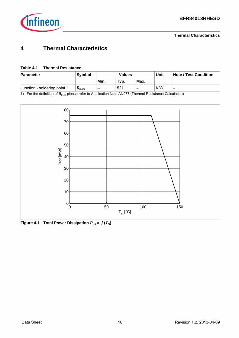
Ptot – 75 mW TS ≤ 111 °CJunction temperature TJ – 150 °C –Storage temperature TStg -55 150 °C –
BFR840L3RHESD
Thermal Characteristics
Data Sheet 10 Revision 1.2, 2013-04-09
4 Thermal Characteristics
Figure 4-1 Total Power Dissipation Ptot = f (TS)
Table 4-1 Thermal ResistanceParameter Symbol Values Unit Note / Test Condition
Min. Typ. Max.Junction - soldering point1)
1) For the definition of RthJS please refer to Application Note AN077 (Thermal Resistance Calculation)RthJS – 521 – K/W –
0 50 100 1500
10
20
30
40
50
60
70
80
TS [°C]
Pto
t [m
W]
BFR840L3RHESD
Electrical Characteristics
Data Sheet 11 Revision 1.2, 2013-04-09
5 Electrical Characteristics
5.1 DC Characteristics
5.2 General AC Characteristics
Table 5-1 DC Characteristics at TA = 25 °CParameter Symbol Values Unit Note / Test Condition
Min. Typ. Max.Collector emitter breakdown voltage V(BR)CEO 2.25 2.6 – V IC = 1 mA, IB = 0
Open baseCollector emitter leakage current ICES – – 400 nA VCE = 1.5 V, VBE = 0
E - B short circuitedCollector base leakage current ICBO – – 400 nA VCB = 1.5 V, IE = 0
Open emitterEmitter base leakage current IEBO – – 10 μA VEB = 0.5 V, IC = 0
Open collectorDC current gain hFE 150 260 450 VCE = 1.8 V, IC = 10 mA
Pulse measured
Table 5-2 General AC Characteristics at TA = 25 °CParameter Symbol Values Unit Note / Test Condition
Min. Typ. Max.Transition frequency fT – 75 – GHz VCE = 1.8 V, IC = 25 mA
f = 2 GHzCollector base capacitance CCB – 52 – fF VCB = 1.8 V, VBE = 0
f = 1 MHzEmitter grounded
Collector emitter capacitance CCE – 0.34 – pF VCE = 1.8 V, VBE = 0f = 1 MHzBase grounded
Emitter base capacitance CEB – 0.34 – pF VEB = 0.4 V, VCB = 0f = 1 MHzCollector grounded
BFR840L3RHESD
Electrical Characteristics
Data Sheet 12 Revision 1.2, 2013-04-09
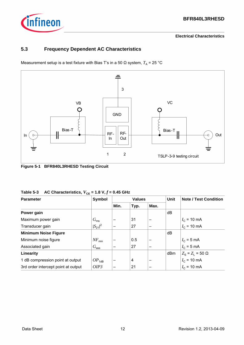
5.3 Frequency Dependent AC Characteristics
Measurement setup is a test fixture with Bias T’s in a 50 Ω system, TA = 25 °C
Figure 5-1 BFR840L3RHESD Testing Circuit
Table 5-3 AC Characteristics, VCE = 1.8 V, f = 0.45 GHzParameter Symbol Values Unit Note / Test Condition
Min. Typ. Max.Power gain dBMaximum power gain Gms – 31 – IC = 10 mATransducer gain |S21|2 – 27 – IC = 10 mAMinimum Noise Figure dBMinimum noise figure NFmin – 0.5 – IC = 5 mAAssociated gain Gass – 27 – IC = 5 mALinearity dBm ZS = ZL = 50 Ω1 dB compression point at output OP1dB – 4 – IC = 10 mA3rd order intercept point at output OIP3 – 21 – IC = 10 mA
Bias -TBias -T
TSLP-3-9 testing circuit
RF-In
RF-Out
VB
In
VC
Out
GND
1 2
3
BFR840L3RHESD
Electrical Characteristics
Data Sheet 13 Revision 1.2, 2013-04-09
Table 5-4 AC Characteristics, VCE = 1.8 V, f = 0.9 GHzParameter Symbol Values Unit Note / Test Condition
Min. Typ. Max.Power gain dBMaximum power gain Gms – 29 – IC = 10 mATransducer gain |S21|2 – 26.5 – IC = 10 mAMinimum Noise Figure dBMinimum noise figure NFmin – 0.55 – IC = 5 mAAssociated gain Gass – 26 – IC = 5 mALinearity dBm ZS = ZL = 50 Ω1 dB compression point at output OP1dB – 4 – IC = 10 mA3rd order intercept point at output OIP3 – 18.5 – IC = 10 mA
Table 5-5 AC Characteristics, VCE = 1.8 V, f = 1.5 GHzParameter Symbol Values Unit Note / Test Condition
Min. Typ. Max.Power gain dBMaximum power gain Gms – 27 – IC = 10 mATransducer gain |S21|2 – 25.5 – IC = 10 mAMinimum Noise Figure dBMinimum noise figure NFmin – 0.55 – IC = 5 mAAssociated gain Gass – 24.5 – IC = 5 mALinearity dBm ZS = ZL = 50 Ω1 dB compression point at output OP1dB – 4 – IC = 10 mA3rd order intercept point at output OIP3 – 17 – IC = 10 mA
Table 5-6 AC Characteristics, VCE = 1.8 V, f = 1.9 GHzParameter Symbol Values Unit Note / Test Condition
Min. Typ. Max.Power gain dBMaximum power gain Gms – 26.5 – IC = 10 mATransducer gain |S21|2 – 25 – IC = 10 mAMinimum Noise Figure dBMinimum noise figure NFmin – 0.60 – IC = 5 mAAssociated gain Gass – 24 – IC = 5 mALinearity dBm ZS = ZL = 50 Ω1 dB compression point at output OP1dB – 4 – IC = 10 mA3rd order intercept point at output OIP3 – 17 – IC = 10 mA

BFR840L3RHESD
Electrical Characteristics
Data Sheet 14 Revision 1.2, 2013-04-09
Table 5-7 AC Characteristics, VCE = 1.8 V, f = 2.4 GHzParameter Symbol Values Unit Note / Test Condition
Min. Typ. Max.Power gain dBMaximum power gain Gms – 25.5 – IC = 10 mATransducer gain |S21|2 – 24 – IC = 10 mAMinimum Noise Figure dBMinimum noise figure NFmin – 0.6 – IC = 5 mAAssociated gain Gass – 22.5 – IC = 5 mALinearity dBm ZS = ZL = 50 Ω1 dB compression point at output OP1dB – 4 – IC = 10 mA3rd order intercept point at output OIP3 – 17 – IC = 10 mA
Table 5-8 AC Characteristics, VCE = 1.8 V, f = 3.5 GHzParameter Symbol Values Unit Note / Test Condition
Min. Typ. Max.Power gain dBMaximum power gain Gms – 23.5 – IC = 10 mATransducer gain |S21|2 – 22 – IC = 10 mAMinimum Noise Figure dBMinimum noise figure NFmin – 0.6 – IC = 5 mAAssociated gain Gass – 20 – IC = 5 mALinearity dBm ZS = ZL = 50 Ω1 dB compression point at output OP1dB – 4 – IC = 10 mA3rd order intercept point at output OIP3 – 18 – IC = 10 mA
Table 5-9 AC Characteristics, VCE = 1.8 V, f = 5.5 GHzParameter Symbol Values Unit Note / Test Condition
Min. Typ. Max.Power gain dBMaximum power gain Gms – 22 – IC = 10 mATransducer gain |S21|2 – 19 – IC = 10 mAMinimum Noise Figure dBMinimum noise figure NFmin – 0.65 – IC = 5 mAAssociated gain Gass – 16.5 – IC = 5 mALinearity dBm ZS = ZL = 50 Ω1 dB compression point at output OP1dB – 4 – IC = 10 mA3rd order intercept point at output OIP3 – 18 – IC = 10 mA
BFR840L3RHESD
Electrical Characteristics
Data Sheet 15 Revision 1.2, 2013-04-09
Note:
1. OIP3 value depends on the termination of all intermodulation frequency components. The termination used for this measurement is 50 Ω from 0.2 MHz to 12 GHz.
Table 5-10 AC Characteristics, VCE = 1.8 V, f = 10 GHzParameter Symbol Values Unit Note / Test Condition
Min. Typ. Max.Power gain dBMaximum power gain Gma – 16 – IC = 10 mATransducer gain |S21|2 – 13 – IC = 10 mAMinimum Noise Figure dBMinimum noise figure NFmin – 0.9 – IC = 5 mAAssociated gain Gass – 11.5 – IC = 5 mALinearity dBm ZS = ZL = 50 Ω1 dB compression point at output OP1dB – 3 – IC = 10 mA3rd order intercept point at output OIP3 – 17 – IC = 10 mA
Table 5-11 AC Characteristics, VCE = 1.8 V, f = 12 GHzParameter Symbol Values Unit Note / Test Condition
Min. Typ. Max.Power gain dBMaximum power gain Gma – 13.5 – IC = 10 mATransducer gain |S21|2 – 10 – IC = 10 mAMinimum Noise Figure dBMinimum noise figure NFmin – 1.1 – IC = 5 mAAssociated gain Gass – 12 – IC = 5 mALinearity dBm ZS = ZL = 50 Ω1 dB compression point at output OP1dB – 3 – IC = 10 mA3rd order intercept point at output OIP3 – 17 – IC = 10 mA
BFR840L3RHESD
Electrical Characteristics
Data Sheet 16 Revision 1.2, 2013-04-09
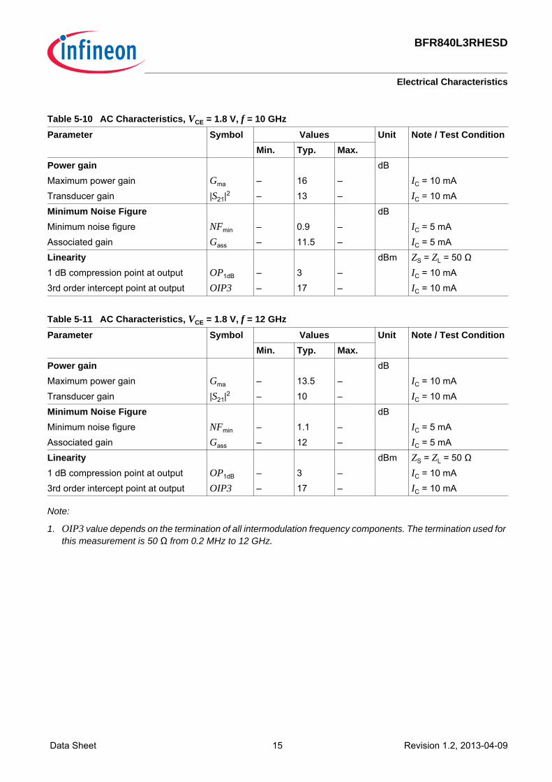
5.4 Characteristic DC Diagrams
Figure 5-2 Collector Current vs. Collector Emitter Voltage IC = f (VCE), IB = Parameter
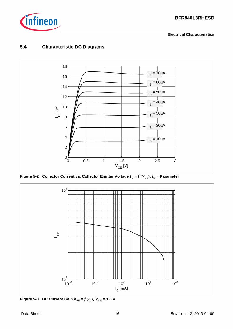
Figure 5-3 DC Current Gain hFE = f (IC), VCE = 1.8 V
0 0.5 1 1.5 2 2.5 30
2
4
6
8
10
12
14
16
18
VCE
[V]
I C [m
A]
IB = 10µA
IB = 20µA
IB = 30µA
IB = 40µA
IB = 50µA
IB = 60µA
IB = 70µA
10−2
10−1
100
101
102
102
103
IC
[mA]
h FE
BFR840L3RHESD
Electrical Characteristics
Data Sheet 17 Revision 1.2, 2013-04-09
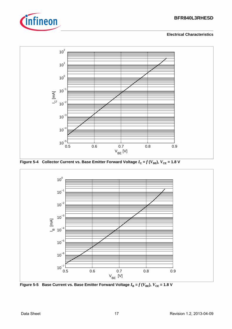
Figure 5-4 Collector Current vs. Base Emitter Forward Voltage IC = f (VBE), VCE = 1.8 V
Figure 5-5 Base Current vs. Base Emitter Forward Voltage IB = f (VBE), VCE = 1.8 V
0.5 0.6 0.7 0.8 0.910
−5
10−4
10−3
10−2
10−1
100
101
102
VBE
[V]
I C [m
A]
0.5 0.6 0.7 0.8 0.910
−7
10−6
10−5
10−4
10−3
10−2
10−1
100
VBE
[V]
I B [m
A]
BFR840L3RHESD
Electrical Characteristics
Data Sheet 18 Revision 1.2, 2013-04-09
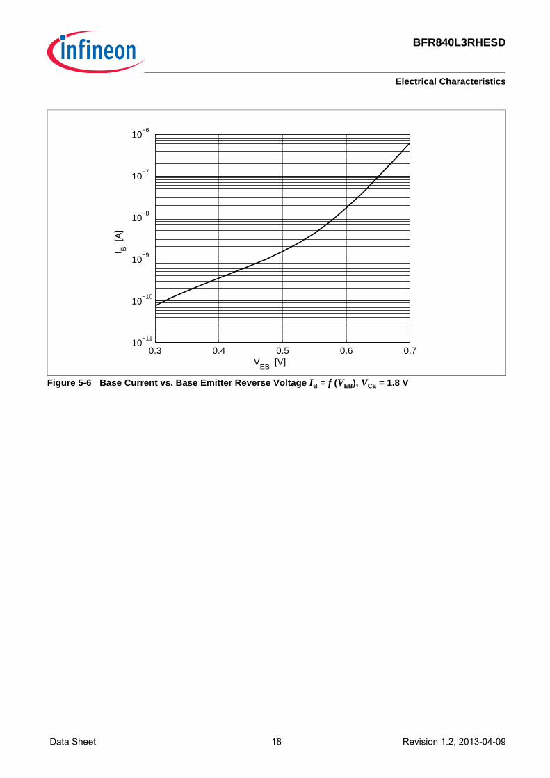
Figure 5-6 Base Current vs. Base Emitter Reverse Voltage IB = f (VEB), VCE = 1.8 V
0.3 0.4 0.5 0.6 0.710
−11
10−10
10−9
10−8
10−7
10−6
VEB
[V]
I B [A
]
BFR840L3RHESD
Electrical Characteristics
Data Sheet 19 Revision 1.2, 2013-04-09
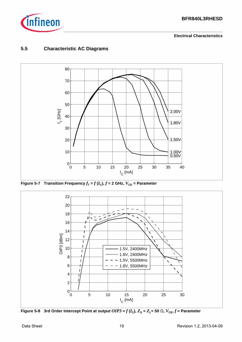
5.5 Characteristic AC Diagrams
Figure 5-7 Transition Frequency fT = f (IC), f = 2 GHz, VCE = Parameter
Figure 5-8 3rd Order Intercept Point at output OIP3 = f (IC), ZS = ZL= 50 Ω, VCE, f = Parameter
0 5 10 15 20 25 30 35 400
10
20
30
40
50
60
70
80
IC
[mA]
f T [G
Hz] 2.00V
1.80V
1.50V
1.00V 0.50V
0 5 10 15 20 25 300
2
4
6
8
10
12
14
16
18
20
22
IC
[mA]
OIP
3 [d
Bm
]
1.5V, 2400MHz1.8V, 2400MHz1.5V, 5500MHz1.8V, 5500MHz
BFR840L3RHESD
Electrical Characteristics
Data Sheet 20 Revision 1.2, 2013-04-09
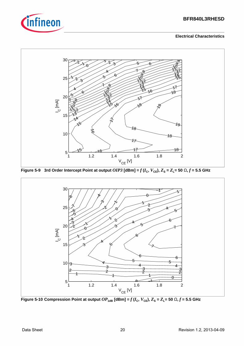
Figure 5-9 3rd Order Intercept Point at output OIP3 [dBm] = f (IC, VCE), ZS = ZL= 50 Ω, f = 5.5 GHz
Figure 5-10 Compression Point at output OP1dB [dBm] = f (IC, VCE), ZS = ZL= 50 Ω, f = 5.5 GHz
−3−2
−1 0
1
1
2
2
3
3
4
4
5
5
5
6
6
6
7
7
7
8
8
8
8
9
9
9
9
10
10
10
10
11
11
11
11
12
12
12
12
13
13
13
13
14
14
14
14
15
15
15
15
15
1616
16
16
17
17
17
17
17
18
18
18
18
19
19
18
VCE
[V]
I C [m
A]
1 1.2 1.4 1.6 1.8 25
10
15
20
25
30
−8−7
−6−5
−4
−4
−3
−3
−2
−2
−1
−1
−1
−1
0
0
0
00
1
1
1
1
111
2
2
2
2222
3
3
3
3333 44
4
4
4
4
55
5
5
5
66
6
6
7
7
VCE
[V]
I C [m
A]
1 1.2 1.4 1.6 1.8 25
10
15
20
25
30
BFR840L3RHESD
Electrical Characteristics
Data Sheet 21 Revision 1.2, 2013-04-09
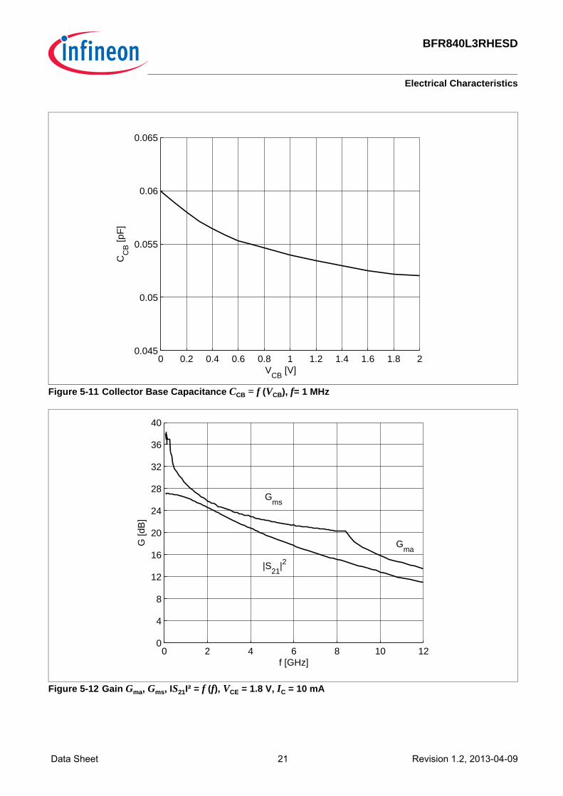
Figure 5-11 Collector Base Capacitance CCB = f (VCB), f= 1 MHz
Figure 5-12 Gain Gma, Gms, IS21I² = f (f), VCE = 1.8 V, IC = 10 mA
0 0.2 0.4 0.6 0.8 1 1.2 1.4 1.6 1.8 20.045
0.05
0.055
0.06
0.065
VCB
[V]
CC
B [p
F]
0 2 4 6 8 10 120
4
8
12
16
20
24
28
32
36
40
f [GHz]
G [d
B]
Gms
Gma
|S21
|2
BFR840L3RHESD
Electrical Characteristics
Data Sheet 22 Revision 1.2, 2013-04-09
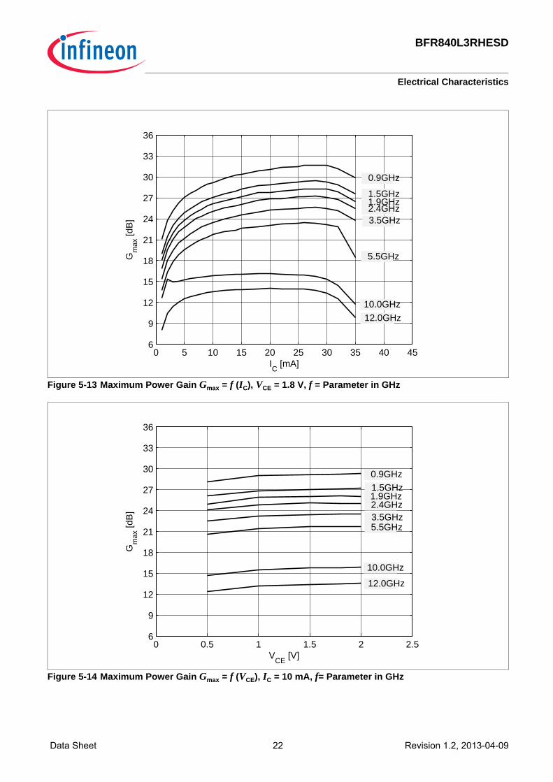
Figure 5-13 Maximum Power Gain Gmax = f (IC), VCE = 1.8 V, f = Parameter in GHz
Figure 5-14 Maximum Power Gain Gmax = f (VCE), IC = 10 mA, f= Parameter in GHz
0 5 10 15 20 25 30 35 40 456
9
12
15
18
21
24
27
30
33
36
IC
[mA]
Gm
ax [d
B]
0.9GHz
1.5GHz 1.9GHz 2.4GHz 3.5GHz
5.5GHz
10.0GHz
12.0GHz
0 0.5 1 1.5 2 2.56
9
12
15
18
21
24
27
30
33
36
VCE
[V]
Gm
ax [d
B]
0.9GHz
1.5GHz 1.9GHz 2.4GHz 3.5GHz 5.5GHz
10.0GHz
12.0GHz
BFR840L3RHESD
Electrical Characteristics
Data Sheet 23 Revision 1.2, 2013-04-09
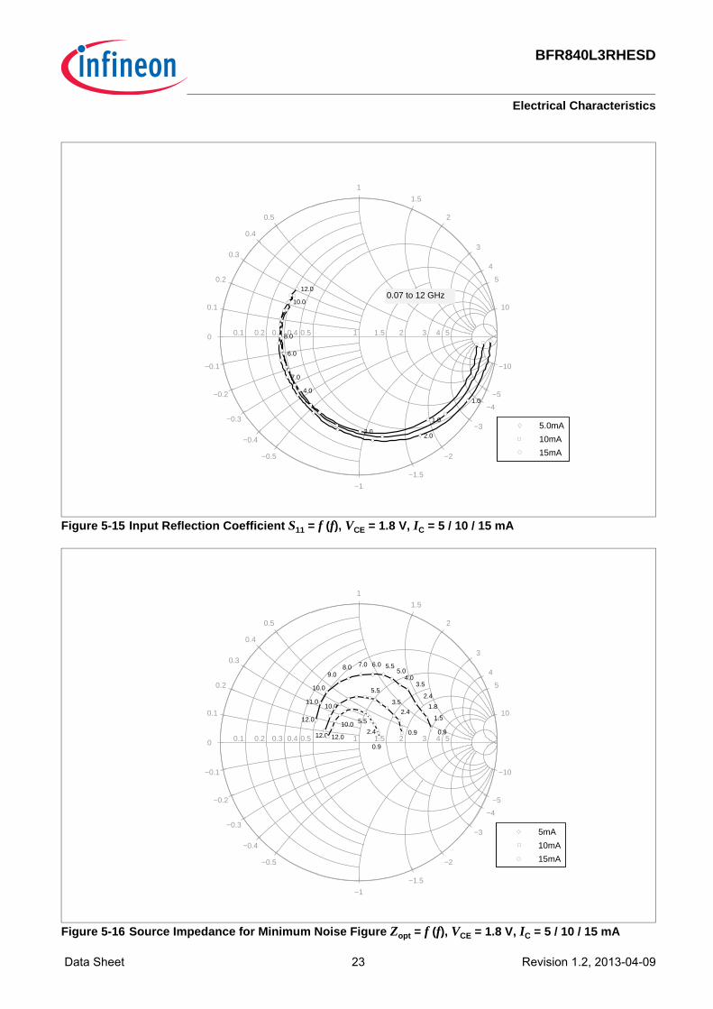
Figure 5-15 Input Reflection Coefficient S11 = f (f), VCE = 1.8 V, IC = 5 / 10 / 15 mA
Figure 5-16 Source Impedance for Minimum Noise Figure Zopt = f (f), VCE = 1.8 V, IC = 5 / 10 / 15 mA
10.1 0.2 0.3 0.4 0.5 21.5 3 4 50
1
−1
1.5
−1.5
2
−2
3
−3
4
−4
5
−5
10
−10
0.5
−0.5
0.1
−0.1
0.2
−0.2
0.3
−0.3
0.4
−0.4
1.0
2.0
7.0
1.0
2.0
4.0
6.0
10.0
12.00.07 to 12 GHz
8.0
5.0mA
10mA
15mA
10.1 0.2 0.3 0.4 0.5 21.5 3 4 50
1
−1
1.5
−1.5
2
−2
3
−3
4
−4
5
−5
10
−10
0.5
−0.5
0.1
−0.1
0.2
−0.2
0.3
−0.3
0.4
−0.4
0.9
1.5
1.8
2.4
3.54.0
5.05.56.07.08.0
9.0
10.0
11.0
12.0
0.9
2.4
3.5
5.5
10.0
12.0
0.9
2.4
5.510.0
12.0
5mA
10mA
15mA
BFR840L3RHESD
Electrical Characteristics
Data Sheet 24 Revision 1.2, 2013-04-09
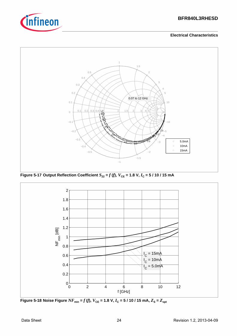
Figure 5-17 Output Reflection Coefficient S22 = f (f), VCE = 1.8 V, IC = 5 / 10 / 15 mA
Figure 5-18 Noise Figure NFmin = f (f), VCE = 1.8 V, IC = 5 / 10 / 15 mA, ZS = Zopt
10.1 0.2 0.3 0.4 0.5 21.5 3 4 50
1
−1
1.5
−1.5
2
−2
3
−3
4
−4
5
−5
10
−10
0.5
−0.5
0.1
−0.1
0.2
−0.2
0.3
−0.3
0.4
−0.4
1.0
2.03.0
4.0
6.0
8.0
10.0
12.0
1.01.0
0.07 to 12 GHz
5.0mA
10mA
15mA
0 2 4 6 8 10 120
0.2
0.4
0.6
0.8
1
1.2
1.4
1.6
1.8
2
f [GHz]
NF
min
[dB
]
IC
= 5.0mA
IC
= 10mA
IC
= 15mA
BFR840L3RHESD
Electrical Characteristics
Data Sheet 25 Revision 1.2, 2013-04-09
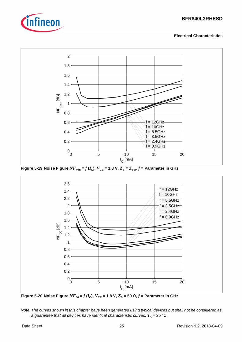
Figure 5-19 Noise Figure NFmin = f (IC), VCE = 1.8 V, ZS = Zopt, f = Parameter in GHz
Figure 5-20 Noise Figure NF50 = f (IC), VCE = 1.8 V, ZS = 50 Ω, f = Parameter in GHz
Note: The curves shown in this chapter have been generated using typical devices but shall not be considered as a guarantee that all devices have identical characteristic curves. TA = 25 °C.
0 5 10 15 200
0.2
0.4
0.6
0.8
1
1.2
1.4
1.6
1.8
2
IC
[mA]
NF
min
[dB
]
f = 0.9GHzf = 2.4GHzf = 3.5GHzf = 5.5GHzf = 10GHzf = 12GHz
0 5 10 15 200
0.2
0.4
0.6
0.8
1
1.2
1.4
1.6
1.8
2
2.2
2.4
2.6
IC
[mA]
NF
50 [d
B]
f = 0.9GHzf = 2.4GHzf = 3.5GHzf = 5.5GHz
f = 10GHzf = 12GHz
BFR840L3RHESD
Simulation Data
Data Sheet 26 Revision 1.2, 2013-04-09
6 Simulation Data
For the SPICE Gummel Poon (GP) model as well as for the S-parameters (including noise parameters) pleaserefer to our internet website. Please consult our website and download the latest versions before actually startingyour design.You find the BFR840L3RHESD SPICE GP model in the internet in MWO- and ADS-format, which you can importinto these circuit simulation tools very quickly and conveniently. The model already contains the packageparasitics and is ready to use for DC and high frequency simulations. The terminals of the model circuit correspondto the pin configuration of the device.The model parameters have been extracted and verified up to 12 GHz using typical devices. TheBFR840L3RHESD SPICE GP model reflects the typical DC- and RF-performance within the limitations which aregiven by the SPICE GP model itself. Besides the DC characteristics all S-parameters in magnitude and phase, aswell as noise figure (including optimum source impedance, equivalent noise resistance and flicker noise) andintermodulation have been extracted.
BFR840L3RHESD
Package Information TSLP-3-9
Data Sheet 27 Revision 1.2, 2013-04-09
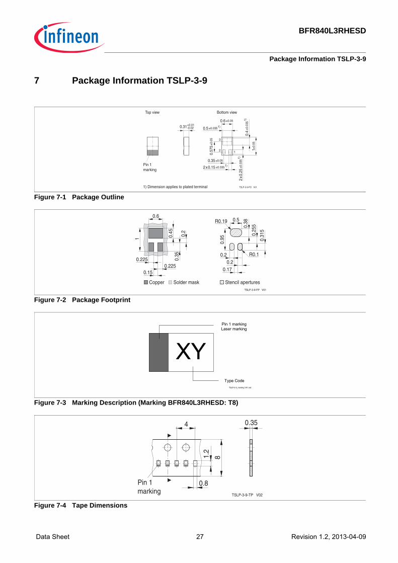
7 Package Information TSLP-3-9
Figure 7-1 Package Outline
Figure 7-2 Package Footprint
Figure 7-3 Marking Description (Marking BFR840L3RHESD: T8)
Figure 7-4 Tape Dimensions
TSLP-3-9-PO V01
Pin 1marking
Top view Bottom view
2 1
±0.0350.5
3
0.57
5
1)
±0.0
350.
41)
±0.0
352
x0.2
51)
0.35
±0.0352x0.15 1)
1) Dimension applies to plated terminal
0.31-0.02+0.01
±0.0
5
±0.05
±0.0
51
0.6 ±0.05
Stencil aperturesCopper Solder mask
0.38
0.20.
315
0.95
0.5
0.17
0.25
5
0.2
0.45
0.225
1
0.6
0.2250.15
0.35
0.2
R0.1
R0.19
TSLP-3-9-FP V01
TSLP-3-9_marking V01.vsd
Pin 1 markingLaser marking
Type Code
XY
TSLP-3-9-TP V02
0.8
4
1.2
0.35
Pin 1marking
8