Embed Size (px)
Citation preview
.
Magnetic field effects onthe local tunneling conductivity ofLa0.75Ca0.25MnO3/MgO thin films
Dissertationzur Erlangung des Doktorgrades
der Mathematisch-Naturwissenschaftlichen Fakultätender Georg-August-Universität zu Göttingen
vorgelegt von
Sigrun Antje Köster
aus
Braunschweig
Göttingen 2007

.
D7
Referent: Prof. Dr. Konrad SamwerKorreferent: PD Dr. Christian JooßTag der Disputation: 10. Oktober 2007
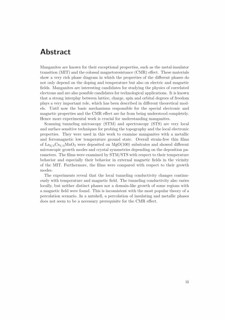
Abstract
Manganites are known for their exceptional properties, such as the metal-insulatortransition (MIT) and the colossal magnetoresistance (CMR) effect. These materialsshow a very rich phase diagram in which the properties of the different phases donot only depend on the doping and temperature but also on electric and magneticfields. Manganites are interesting candidates for studying the physics of correlatedelectrons and are also possible candidates for technological applications. It is knownthat a strong interplay between lattice, charge, spin and orbital degrees of freedomplays a very important role, which has been described in different theoretical mod-els. Until now the basic mechanisms responsible for the special electronic andmagnetic properties and the CMR effect are far from being understood completely.Hence more experimental work is crucial for understanding manganites.
Scanning tunneling microscopy (STM) and spectroscopy (STS) are very localand surface sensitive techniques for probing the topography and the local electronicproperties. They were used in this work to examine manganites with a metallicand ferromagnetic low temperature ground state. Overall strain-free thin filmsof La3/4Ca1/4MnO3 were deposited on MgO(100) substrates and showed differentmicroscopic growth modes and crystal symmetries depending on the deposition pa-rameters. The films were examined by STM/STS with respect to their temperaturebehavior and especially their behavior in external magnetic fields in the vicinityof the MIT. Furthermore, the films were compared with respect to their growthmodes.
The experiments reveal that the local tunneling conductivity changes continu-ously with temperature and magnetic field. The tunneling conductivity also varieslocally, but neither distinct phases nor a domain-like growth of some regions witha magnetic field were found. This is inconsistent with the most popular theory of apercolation scenario. In a nutshell, a percolation of insulating and metallic phasesdoes not seem to be a necessary prerequisite for the CMR effect.
iii

iv
Zusammenfassung
Die Manganate sind für ihre besonderen Eigenschaften, wie den Metal-IsolatorÜbergang (MIT) und den kolossalem Magnetowiderstandseffekt (CMR), bekannt.Diese Materialien zeigen ein sehr reichhaltiges Phasendiagramm, wobei die Eigen-schaften der verschiedenen Phasen nicht nur von der Dotierung und der Temperaturabhängig sind, sondern auch von elektrischen und magnetischen Feldern. Die Man-ganate sind interessante Kandidaten für das Studium der Physik korrelierter Elek-tronen als auch für eventuelle technische Anwendungen. Es ist bereits bekannt, dassdie Wechselwirkung der verschiedenen Freiheitsgrade (Gitter, Ladung, Spin undOrbital) eine sehr wichtige Rolle spielen. Dies wird in verschiedenen theoretischenModellen beschrieben. Dennoch sind die Mechanismen, die für die elektronischenund magnetischen Eigenschaften verantwortlich sind noch lange nicht vollständigverstanden. Weitere experimentelle Untersuchungen sind daher unentbehrlich fürdas Verständnis der Manganate.
Rastertunnelmikroskopie (STM) und -spektroskopie (STS) sind sehr lokale undoberflächensensitive Verfahren, um die Topografie und die lokalen elektronischenEigenschaften einer Probe zu erfassen. In dieser Arbeit wurden Manganate miteinem metallischen und ferromagnetischen Grundzustand bei tiefen Temperaturenuntersucht. Spannungsfreie dünne La3/4Ca1/4MnO3-Filme wurden auf MgO(100)Substraten deponiert und zeigten je nach Herstellungsparametern unterschiedlicheWachstumsmoden und Kristallsymmetrien. Die Proben wurde mittels STM undSTS in Abhängigkeit der Temperatur und insbesondere von äußeren magnetis-chen Feldern im Bereich des MIT untersucht und bezüglich ihrer Wachstumsmodenmiteinander verglichen.
Die Experimente zeigen, dass sich die lokale Tunnelleitfähigkeit kontinuierlichmit der Temperatur und dem Magnetfeld ändert. Die Tunnelleitfähigkeit variiertauch lokal, allerdings sind keine einzelnen klar unterscheidbaren Phasen zu sehenund es ist kein Domänenwachstum von einzelnen Bereichen in Abhängigkeit vomMagnetfeld zu beobachten. Dies entspricht nicht der verbreiteten Theorie einesPerkolationsübergangs. Kurz gesagt, scheint also ein Perkolationsübergang miteiner isolierender und metallischer Phase nicht notwendigerweise der Ursprung desCMR zu sein.
v

vi
Contents
Abstract iii
Zusammenfassung v
Glossary ix
1. Introduction 1
2. Manganites 5
2.1. Fundamental properties . . . . . . . . . . . . . . . . . . . . . . . . . 52.1.1. Crystal structure . . . . . . . . . . . . . . . . . . . . . . . . . 82.1.2. Basic electronic properties . . . . . . . . . . . . . . . . . . . . 92.1.3. Magnetic properties, exchange mechanisms and orbital ordering 112.1.4. Beyond the simple mechanisms: Polarons . . . . . . . . . . . 15
2.2. Phase separation . . . . . . . . . . . . . . . . . . . . . . . . . . . . . 162.3. The case of LCMO . . . . . . . . . . . . . . . . . . . . . . . . . . . . 19
3. STM and STS - Fundamental considerations 27
3.1. Basic concepts of STM . . . . . . . . . . . . . . . . . . . . . . . . . . 273.1.1. Topographic imaging . . . . . . . . . . . . . . . . . . . . . . . 31
3.2. Spectroscopy . . . . . . . . . . . . . . . . . . . . . . . . . . . . . . . 33
4. Preparation and characterization techniques 37
4.1. Metal organic aerosol deposition . . . . . . . . . . . . . . . . . . . . 374.2. Standard characterization . . . . . . . . . . . . . . . . . . . . . . . . 39
4.2.1. X-Ray scattering . . . . . . . . . . . . . . . . . . . . . . . . . 394.2.2. Resistance measurements . . . . . . . . . . . . . . . . . . . . 414.2.3. Magnetization measurement . . . . . . . . . . . . . . . . . . . 42
5. STM and STS – Setup and experiments 47
5.1. General considerations about STM/STS measurements . . . . . . . . 475.1.1. Measuring modes . . . . . . . . . . . . . . . . . . . . . . . . . 475.1.2. Mechanical damping and electrical noise . . . . . . . . . . . . 49
5.2. The Cryogenic SFM by Omicron . . . . . . . . . . . . . . . . . . . . 505.2.1. Inner system: The microscope and connected components . . 515.2.2. Outer part: Cryostat, UHV system and environment . . . . . 545.2.3. Operation, electronics and important improvements . . . . . 585.2.4. Mechanical insulation and damping of the system . . . . . . . 59
5.3. Computer based analysis . . . . . . . . . . . . . . . . . . . . . . . . . 61
vii
Contents viii
6. The basic sample properties 676.1. Growth mode . . . . . . . . . . . . . . . . . . . . . . . . . . . . . . . 676.2. Structural properties . . . . . . . . . . . . . . . . . . . . . . . . . . . 686.3. The metal-insulator transition . . . . . . . . . . . . . . . . . . . . . . 716.4. Magnetic properties and magnetoresistance . . . . . . . . . . . . . . 72
7. STM and STS results 777.1. Film with three dimensional growth mode . . . . . . . . . . . . . . . 78
7.1.1. Histogram analysis . . . . . . . . . . . . . . . . . . . . . . . . 787.1.2. Temperature dependence . . . . . . . . . . . . . . . . . . . . 797.1.3. Magnetic field dependencies . . . . . . . . . . . . . . . . . . . 807.1.4. Summary . . . . . . . . . . . . . . . . . . . . . . . . . . . . . 89
7.2. Film with layered growth . . . . . . . . . . . . . . . . . . . . . . . . 917.2.1. Topographic details . . . . . . . . . . . . . . . . . . . . . . . 917.2.2. Temperature dependence . . . . . . . . . . . . . . . . . . . . 917.2.3. Field dependence . . . . . . . . . . . . . . . . . . . . . . . . . 957.2.4. Voltage dependence . . . . . . . . . . . . . . . . . . . . . . . 1027.2.5. Summary . . . . . . . . . . . . . . . . . . . . . . . . . . . . . 104
8. Discussion 1078.1. The samples and their structural differences . . . . . . . . . . . . . . 107
8.1.1. Thin film growth . . . . . . . . . . . . . . . . . . . . . . . . . 1078.1.2. Ordering tendencies . . . . . . . . . . . . . . . . . . . . . . . 108
8.2. Spectroscopy . . . . . . . . . . . . . . . . . . . . . . . . . . . . . . . 1118.2.1. Magnetic effects on the local tunneling conductance . . . . . 1118.2.2. Additional remarks about the spectroscopic data . . . . . . . 115
8.3. Phase separation . . . . . . . . . . . . . . . . . . . . . . . . . . . . . 1168.3.1. Is there a distinct two phase behavior? . . . . . . . . . . . . . 1178.3.2. Size effects and correlations . . . . . . . . . . . . . . . . . . . 1198.3.3. Comparison with the models . . . . . . . . . . . . . . . . . . 121
8.4. Comparison with other STM and STS studies . . . . . . . . . . . . . 1238.5. The metal-insulator transition in manganites . . . . . . . . . . . . . 127
9. Summary and outlook 1339.1. Future work . . . . . . . . . . . . . . . . . . . . . . . . . . . . . . . . 134
A. Sample data 137
B. Experimental supplements 139B.1. STM and MFM on PCMO . . . . . . . . . . . . . . . . . . . . . . . 139B.2. LCMO tips . . . . . . . . . . . . . . . . . . . . . . . . . . . . . . . . 141B.3. Remarks on other effects in STS . . . . . . . . . . . . . . . . . . . . 143B.4. Tip etching procedure . . . . . . . . . . . . . . . . . . . . . . . . . . 143
C. Mathematical considerations 149C.1. Autocorrelation function . . . . . . . . . . . . . . . . . . . . . . . . . 149

Glossary
Abbreviations
3D Three dimensional (grain-like) growth.
ac Alternating current.
ACEC Acetylacetonate, negatively charged, used a ligand for metal-chelatecomplex compounds.
ADC Analog digital converter.
AF Antiferromagnetic phase.
AFM Atomic force microscope.
AMR Anisotropic magneto resistance.
CMR Colossal magneto resistance.
CO Charge ordered phase.
DAC Digital analog converter.
dc Direct current.
DE Double exchange.
DMFA Dimethylformamide.
DMFT Dynamical mean field theory.
DOS Density of States.
ED Electron diffraction.
FFT Fast Fourier Transform.
FM Ferromagnetic phase.
FT Fourier Transform.
FWHM Full width of half maximum.
GMR Giant magneto resistance.
HOPG Highly oriented pyrolytic graphite.
ix

GLOSSARY x
HRTEM High resolution transmission electron microscopy.
I Insulating phase.
IDL Interactive data language, Research Systems, Inc.
IVC Current voltage converter.
LCMO La0.75Ca0.25MnO3 (results and discussion); LaxCa1−xMnO3 (in generalterms).
LDOS Local Density of States.
LL Layer-by-layer growth.
LL-O Layer-by-layer growth with an A-site ordering.
M Metallic phase.
Mn+ Metal ion as chemical symbol with charge n+.
MAD Metal organic aerosol deposition.
MFM Magnetic force microscope.
MIT Metal insulator transition.
MOCVD Metal organic chemical vapor deposition.
NV Needle valve.
OVC Outer vacuum shell (Omicron cryostat).
PM Paramagnetic phase.
PPMS Physical Property Measurement System, Quantum Design, here usedfor resistance measurements.
rf Radio frequency.
rms Root mean square.
RT Room temperature (300K).
SAXS Small angle X-ray scattering.
SE Superexchange.
SFM Scanning force microscope.
SPM Scanning probe microscope.
SQUID Superconducting Quantum Interference Device, in this work a SQUID-magnetometer from Quantum Design was used for magnetization mea-surements.

xi GLOSSARY
STM Scanning tunneling microscope.
STS Scanning tunneling spectroscopy.
TEM Transmission electron microscopy.
TMR Tunnel magneto resistance.
TSP Titanium sublimation pump.
UHV Ultra high vacuum.
VIC Voltage current converter.
VTI Variable temperature insert.
WAXS Wide angle X-ray scattering.
XRD X-ray diffraction.
XRR X-ray reflectometry.
Symbols
a, b Lattice parameters (unit cell or pseudo cubic cell), in general to describethe in-plane parameters.
A Amplitude, parameter in exponential decay.
c Lattice parameter (unit cell or pseudo-cubic cell), in general to describeout-of-plane parameter.
Cfg Convolution between functions f and g.
C Correlation function, capacitance (experimental part), sometimes aconstant.
C(r) Radial correlation function.
dhkl Spacing of lattice planes corresponding to the Miller indices hkl.
d Film thickness.
e Electron charge.
E Energy, generally as fixed value.
EF Fermi energy.
F± Operator for Fourier Transform (+) and its inverse (−).
f, g Functions.
f∗(x) Complex conjugate of f .

GLOSSARY xii
f Fourier transform of f .
F Force.
f(ǫ) Fermi-Dirac distribution.
hkl Miller indices.
I0 Current (predetermined).
I Current/Tunneling current.
j, l Indices (integers) for discrete FT.
~ki/r Incident (i) and reflected (r) wave vectors for X-ray geometry.
L Self inductance.
m (Electron) Mass, interference maxima.
mi Number of interference maximum (integer).
Mµν Matrix elements, connecting the states within the tunneling equation.
m0 Electron mass.
n Refractive index.
NA Avogadro number (6.02217·1023).
Ne Electron density.
N Integer number.
~q Scattering vector of X-rays.
re Classical electron radius.
r1/2 Radii for distance of sample contacts.
r Radius (used in correlation functions).
rl Correlation length (here: exponential decay length of radial correla-tion).
~r Spacial position vector.
t Time.
T Temperature.
U, V Voltage.
u Variable, like x.
x, y Coordinates (in plane).
z Coordinate (perpendicular to plane), height.
Z Transfer function.

xiii GLOSSARY
Greek Symbols
β Imaginary part of refractive index, describing absorption.
χ Error.
δ Real part of refractive index, describing dispersion.
ǫ Energy, in general as variable.
κ Exponential decaying constant for wavefunctions in classically forbid-den region.
λ Wavelength of X-rays (for CuKα=1.54184·10−8 cm).
µ, ν Indices, corresponding to the energy states of the different electrodesin a tunneling junction.
µ Attenuation coefficient.
Φ Magnetic flux.
Φext Magnetic flux from an external source.
Φ0 Flux quantum.
Φµ,ν ; Φs,t Work functions for tunneling electrodes (tip,sample).
Ψµ,ν Wave functions for tunneling electrodes.
ρ Mass density, resistivity.
ρ(ǫ) Density of states as function of energy.
σ Roughness (rms), tunneling conductivity dI/dU .
σp Peak (mean) conductivity of histograms from tunneling conductivities.
Θ Angle of incidence (with respect to the surface) for XRD.
Θt Angle of total reflection for XRR.

GLOSSARY xiv
1. Introduction
In solid state physics as well as in industrial technology the dimensions of the re-search on structure, electronics and magnetism get smaller and smaller and theword “nano” has become a representative classifying these fields. The so-calledmagneto resistance (MR) effects belong into this regime, since they deal aboutmagnetism on the nanometer scale and are involved in devices utilized in nano-technology. The MR effect appears as changes in the resistivity ρ of a sample in-duced by an applied magnetic field H. These effects can be very large and underlyvery different mechanisms, not all of them being finally understood. In manganitesthe MR effect is caused by an interplay of microscopic interactions, and take effecton the properties on a nanometer scale, therefore the topic of this work can be in-cluded in the widespread areas of nano-scale magnetism and nano-scale electronicfeatures.
Manganites are manganese oxide compounds mixed with rear earth and/or tran-sition metal elements like La0.75Ca0.25MnO3 . They show peculiar magnetic andelectronic properties. Since the discovery of the colossal magneto resistance (CMR)effect in manganites [7], they can be regarded as materials of widespread interestin solid state physics and materials sciences. The manganites belong to the corre-lated electron systems, which are interesting for basic research with respect to theunderstanding of the specific microscopic interactions and are still far away frombeing understood. In correlated electron systems the individual charge carriers arenot independent from each other, like it is the case in a simple metal as copper witha nearly free electron gas, but their behavior is coupled. This is due to the factthat correlated electron materials consist of d- or f–electron systems, which havequite localized orbitals. Therefore the Coulomb repulsion becomes very importantand the behavior of one electron depends on all the others.
A basic model describing correlated electron systems is the Hubbard model [4],but the real cases are usually much more complex. An intricate system of lattice,charge, orbital and spin degrees of freedom makes the manganites to fascinatingcandidates in the context of electronic transport and magnetism in correlated elec-tron materials. Complex phase diagrams with regions of very different properties,that is insulating, metallic, ferromagnetic, antiferromagnetic or charge and orbitalordered phases can be observed.
Ferromagnetic manganites show a metal to insulator transition together with aferromagnetic to paramagnetic transition, for which the transition temperatures canbe tuned by the composition. The largest values for the CMR effect are observed inthe temperature region of these transitions, which are coupled to each other. Thedriving mechanism of this metal-insulator transition has not been fully understood
1
2
and remarkably the CMR effect becomes larger for those compounds showing higherresidual resistivities.
It is known already that the charge transport is somehow coupled to the mag-netic properties via the superexchange and double exchange mechanisms, whichevoke either an antiferromagnetic or ferromagnetic coupling of the core spins of themanganese atoms via the oxygen atoms in between. A movement of the chargecarrier is then dependent on the orientations of the spins or more precisely localmoments. This can explain the reduction of the resistivity within magnetic fields,but taking only these exchange mechanisms into account proves to be insufficient.Charge and lattice effects, as Jahn-Teller distortions or polarons, play a crucial role.Additionally, for the CMR effect a phase separation scenario is discussed. The com-petition of a ferromagnetic metallic and an antiferromagnetic insulating phase hasbeen proposed and partially observed in some experiments. It is still under debateif phase separation and percolation is essential for the occurrence of the CMR effect.
Manganites exist as single crystals, polycrystalline bulk samples or as thin filmson very different oxidic substrates. Of course the real intrinsic properties can onlybe observed for single crystalline samples or unstrained thin films, in contrast toextrinsic effects, which are observed for polycrystalline samples due to the grainsizes and interface effects [9]. Since the production of single crystals is not straight-forward, very often thin films are used for the experiments. In addition, they arealso more useful candidates for various applications. The properties of thin filmscannot only be varied by their composition, but also by the substrate on whichthey are deposited.
A lot of models for the metal-insulator transition in manganites exist, but theyare in general too simple to explain the entire system. Therefore it is still neces-sary to perform experimental research on this system. The bulk properties havealready been widely examined, however for the origin of these properties micro-scopic techniques are of relevance. Such a technique is the scanning tunneling mi-croscopy (STM) together with scanning tunneling spectroscopy (STS). With STMthe surface of the sample can be examined on a nanometer scale and STS yieldsinformation about the local electronic properties of the sample. If these observa-tions are done together with the application of magnetic fields, which is a quitechallenging task, it is possible to investigate directly the field induced changes ofthe local properties.
To shed somewhat more light onto this issue was the task of this thesis. Thelocal electronic properties of thin ferromagnetic manganite films were examined.This was done with respect to the occurrence of a phase separation and concerningthe behavior within applied magnetic fields.
Due to their peculiar properties manganite thin films are interesting for tech-nological applications, since they show a variety of magnetoresistance effects andpossess a large spin-polarization. The latter is important for magnetic layer sys-tems. The magneto resistance effects in materials can be used for magnetic fieldsensors, magnetic memories, switches or other devices. For example the giant mag-neto resistance effect (GMR) found in specific layer systems [3], is used in read
3 Bibliography
heads of hard disks [1]. In manganite thin film structures an anisotropic magnetoresistance effect (AMR) was found, that is the resistivity of the film depends onthe direction of the magnetic field with respect to the crystallographic orientations.Since the spin-polarization is very high in manganites, they might be utilized intunneling magneto resistive (TMR) systems [5, 6] as well. For example the TMReffect is used in magnetic random access memory devices (MRAM). A very newfield is the current induced switching in magnetic spin valve systems. One of themagnetic layers is switched by a current, which is applied perpendicular to theplane. Some groups work on manganite based field-effect transistors [8] and ad-ditionally the ferroelectric properties are in the focus of technological research. Asummary of some of the important new materials useful for technological applica-tions is given in [2].
In this work STM and STS measurements were performed mainly in the vicin-ity of the metal-insulator transition on La0.75Ca0.25MnO3 thin films, which weredeposited on MgO substrates by the metal organic aerosol deposition (MAD) tech-nique. To achieve some STS data with a magnetic field applied, a microscopesituated in a cryostat under ultra high vacuum conditions was used. The thesis isstructured as in the following:
The fundamental properties and theories for the basic understanding of mangan-ites are introduced in Chapter 2 together with a review of the most importantliterature. It is followed by a brief summary of the theoretical fundamentals aboutthe STM and STS techniques in Chapter 3. The standard experimental tech-niques used for the thin film deposition and characterization are reviewed in shortin Chapter 4. Then a detailed presentation of the microscope used for this workand its environment is given in Chapter 5. The experimental results are splitinto two parts: Whereas Chapter 6 deals with the basic sample characteristics,Chapter 7 presents the STM and STS results. In Chapter 8 the results arediscussed and the work is finished by a summary and outlook in Chapter 9. Thereferences appear in alphabetical order for each chapter.
Bibliography
[1] Recording heads/head materials. http://www.hitachigst.com/hdd/research/recording_head/headmaterials/index.html, 2007. Hitachi Global Storage Technologies,San Jose, California, USA.
[2] Forschungszentrum Jülich GmbH, Institut für Festkörperforschung. Neue
Materialien für die Informationstechnik, volume 32 of IFF-Ferienkurs.Forschungszentrum Jülich GmbH, 2001.
[3] B. Heinrich and J. A. C. Bland, editors. Ultrathin Magnetic structures II,volume 2. Spinger Verlag (Berlin, Heidelberg), 1994.
[4] J. Hubbard. Electron correlations in narrow energy bands. Proc. Roy. Soc. A,276:238, 1963.

Bibliography 4
[5] J. S. Moodera, L. R. Kinder, T. M. Wong, and T. Meservey. Phys. Rev. Lett.,74:7, 1995.
[6] J. S. Moodera and G. Mathon. J. Magn. Magn. Mat., 200:248, 1999.
[7] R. von Helmolt, J. Wecker, B. Holzapfel, L. Schultz, and K. Samwer. Phys.
Rev. Lett., 71:2331, 1993.
[8] T. Zhao, S. B. Ogale, S. R. Shinde, R. Ramesh, R. Droopad, J. Yu, K. Eisen-beiser, and J. Misewich. Appl. Phys. Lett., 84:750, 2004.
[9] M. Ziese. Rep. Prog. Phys., 56:143, 2002.
2. Manganites
The so called manganites are manganese oxide compounds mixed with rare earthand alkaline earth elements. They show a large variety of structural, resistiveand magnetic properties. These can be attributed to complicated interactions ofcharge, orbital and spin degrees of freedom. Like some other correlated oxides (e.g.the group of vanadium oxides) they show a metal-insulator transition, which canreach room temperature or even higher temperatures depending of the particularcomposition. Additionally large magneto-resistive effects can be observed coupledto the magnetic transitions, which made the manganites very popular in solidstate research. The manganites show in general a rich phase diagram, which givesthe possibility to learn a lot about these transitions and their coupled electronicand magnetic properties. Besides a technical usage of these compounds, theirstudy provides a widespread possibility to gain more insight in correlated electronsystems.
The first interest in manganese oxide compounds came up in 1950, when vanSanten and Jonker reported about an “anomaly” in the resistive behavior of man-ganites [67], the metal-insulator transition (MIT). They also firstly studied thecrystallographic and magnetic properties of these compounds. Some more studiesfollowed [31, 70] including theoretical work by Zener [74], Hasegawa et al. [5] andde Gennes [19]. But the large interest in manganites arose much later, when – dueto higher quality samples – the so called colossal magneto-resistance effect (CMR)with changes in the resistance of up to 100.000% was discovered [69, 8, 46, 60, 41, 9]in thin films and in bulk materials.
In the following the physics of manganites will be briefly reviewed, includingthe main properties, the most important structures and the basic exchange mech-anisms, which are important to understand the complexity evolving in the phasediagrams. One section is addressed to the phase separation, which is very importantfor the present discussions regarding the phase transition. The chapter is orientedat the ferromagnetic compounds and at the end the features of La1−xCaxMnO3 willbe summarized. In conjunction with the results obtained in this work a detaileddiscussion of particular models and a comparison with other results in the literatureis following in the discussion, Chap. 8.
2.1. Fundamental properties
Talking about the manganites the following group of compounds is meant: The par-ent compound is the perovskite ABO3 with Mn on the B-site, for instance LaMnO3
or CaMnO3. The A-site can be split into two groups of elements, for the doping ofthe respective parent compound. The resulting compound is RE1−xAExMnO3 with
5
2.1. Fundamental properties 6
-10000 -5000 0 5000 10000-750-500-250
0250500750
M/V
[em
u/cm
3 ]
Field [Oe]
Hystereses10K
50 100 150 200 250 300
0.0
0.2
0.4
0.6
0.8
1.0M
[em
u10-3
]
T [K]
Magnetization
100 Oe
150 200 250 300
0.00.51.01.52.02.5
R [k
Ω]
T [K]
Resistivity H=0
H=50kOe
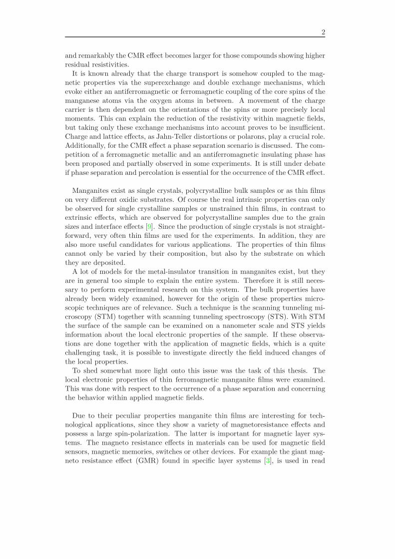
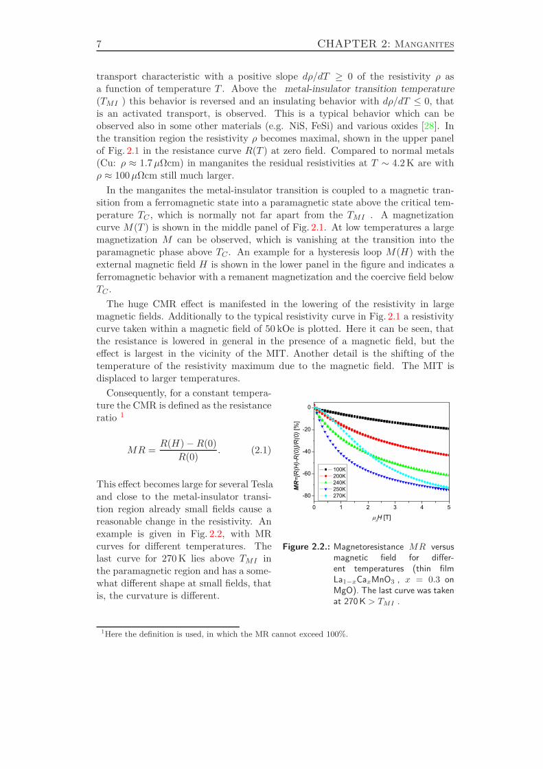
Figure 2.1.: The main features of ferromagnetic manganites. Top: Resistance R versus tem-perature T for a zero and non-zero field (H = 50 kOe) measurement. Mid-dle: Magnetization M versus temperature. Bottom: Hysteresis loop M(H) atT = 10 K. The measurements stem from a La1−xCaxMnO3 thin film for x = 0.3on a MgO substrate.
RE as the trivalent rare earth elements (La, Pr, Nd, Sm, etc.) and AE as divalent al-kaline earth ions (Sr, Ca, Ba). In a ionic model it would be RE3+
1−xAE2+x (Mn3+
1−xMn4+x )O3,
underlining already the important role of the mixed valence on the manganite site,which is – to a large extent – responsible for the widespread properties found. Thelatter will be reviewed in course of the detailed structural and electronic properties.
The properties observed within the manganite family vary from antiferromag-netic insulators (LaMnO3, CaMnO3), over insulating ferromagnets (Pr0.8Ca0.2MnO3)to ferromagnetic metals (La0.75Sr0.25MnO3 , La0.75Ca0.25MnO3 ) and charge order-ing (La7/8Ca1/8MnO3) in their low temperature phase. Most of them undergo aphase transition at a certain temperature with respect to their electronic and mag-netic behavior, which are strongly coupled to each other. Also structural transitionsare observed supplementary. About the basic properties of the different compoundsa lot of review articles can be found, for instance in Refs. [64, 12, 58, 22, 65]. Com-monly the CMR effect is introduced together with the MIT from a ferromagneticmetal to a paramagnetic insulator, like in the case of La0.75Ca0.25MnO3 .
The MIT in the manganites can be described as a transition between a metallic
7 CHAPTER 2: Manganites
transport characteristic with a positive slope dρ/dT ≥ 0 of the resistivity ρ asa function of temperature T . Above the metal-insulator transition temperature
(TMI ) this behavior is reversed and an insulating behavior with dρ/dT ≤ 0, thatis an activated transport, is observed. This is a typical behavior which can beobserved also in some other materials (e.g. NiS, FeSi) and various oxides [28]. Inthe transition region the resistivity ρ becomes maximal, shown in the upper panelof Fig. 2.1 in the resistance curve R(T ) at zero field. Compared to normal metals(Cu: ρ ≈ 1.7µΩcm) in manganites the residual resistivities at T ∼ 4.2 K are withρ ≈ 100µΩcm still much larger.
In the manganites the metal-insulator transition is coupled to a magnetic tran-sition from a ferromagnetic state into a paramagnetic state above the critical tem-perature TC , which is normally not far apart from the TMI . A magnetizationcurve M(T ) is shown in the middle panel of Fig. 2.1. At low temperatures a largemagnetization M can be observed, which is vanishing at the transition into theparamagnetic phase above TC . An example for a hysteresis loop M(H) with theexternal magnetic field H is shown in the lower panel in the figure and indicates aferromagnetic behavior with a remanent magnetization and the coercive field belowTC .
The huge CMR effect is manifested in the lowering of the resistivity in largemagnetic fields. Additionally to the typical resistivity curve in Fig. 2.1 a resistivitycurve taken within a magnetic field of 50 kOe is plotted. Here it can be seen, thatthe resistance is lowered in general in the presence of a magnetic field, but theeffect is largest in the vicinity of the MIT. Another detail is the shifting of thetemperature of the resistivity maximum due to the magnetic field. The MIT isdisplaced to larger temperatures.
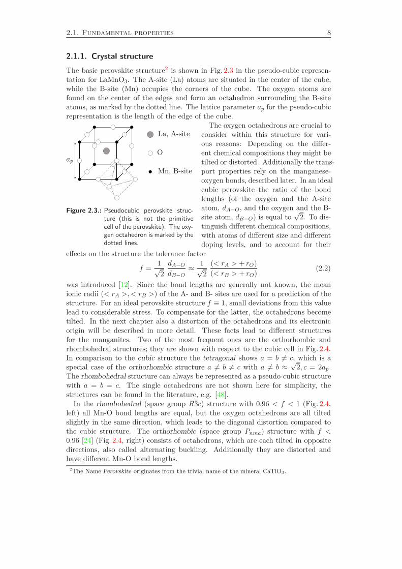
Consequently, for a constant tempera-
0 1 2 3 4 5
-80
-60
-40
-20
0
MR=[R(H
)-R(0
)]/R(0
) [%
]
H [T]
100K 200K 240K 250K 270K
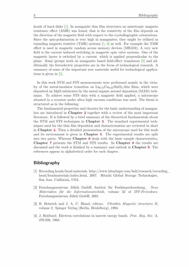
Figure 2.2.: Magnetoresistance MR versusmagnetic field for differ-ent temperatures (thin filmLa1−xCaxMnO3 , x = 0.3 onMgO). The last curve was takenat 270 K > TMI .
ture the CMR is defined as the resistanceratio 1
MR =R(H)−R(0)R(0)
. (2.1)
This effect becomes large for several Teslaand close to the metal-insulator transi-tion region already small fields cause areasonable change in the resistivity. Anexample is given in Fig. 2.2, with MRcurves for different temperatures. Thelast curve for 270 K lies above TMI inthe paramagnetic region and has a some-what different shape at small fields, thatis, the curvature is different.
1Here the definition is used, in which the MR cannot exceed 100%.
2.1. Fundamental properties 8
2.1.1. Crystal structure
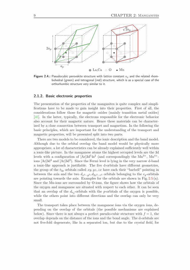
The basic perovskite structure2 is shown in Fig. 2.3 in the pseudo-cubic represen-tation for LaMnO3. The A-site (La) atoms are situated in the center of the cube,while the B-site (Mn) occupies the corners of the cube. The oxygen atoms arefound on the center of the edges and form an octahedron surrounding the B-siteatoms, as marked by the dotted line. The lattice parameter ap for the pseudo-cubicrepresentation is the length of the edge of the cube.
The oxygen octahedrons are crucial to
Mn, B-site
La, A-site
Oap
Figure 2.3.: Pseudocubic perovskite struc-ture (this is not the primitivecell of the perovskite). The oxy-gen octahedron is marked by thedotted lines.
consider within this structure for vari-ous reasons: Depending on the differ-ent chemical compositions they might betilted or distorted. Additionally the trans-port properties rely on the manganese-oxygen bonds, described later. In an idealcubic perovskite the ratio of the bondlengths (of the oxygen and the A-siteatom, dA−O, and the oxygen and the B-site atom, dB−O) is equal to
√2. To dis-
tinguish different chemical compositions,with atoms of different size and differentdoping levels, and to account for their
effects on the structure the tolerance factor
f =1√2
dA−OdB−O
≈ 1√2
(< rA > + rO)(< rB > + rO)
(2.2)
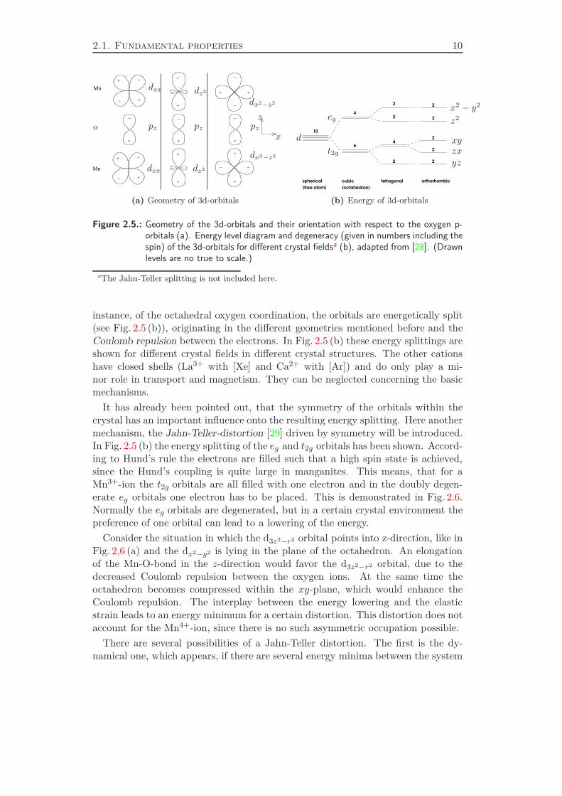
was introduced [12]. Since the bond lengths are generally not known, the meanionic radii (< rA >,< rB >) of the A- and B- sites are used for a prediction of thestructure. For an ideal perovskite structure f ≡ 1, small deviations from this valuelead to considerable stress. To compensate for the latter, the octahedrons becometilted. In the next chapter also a distortion of the octahedrons and its electronicorigin will be described in more detail. These facts lead to different structuresfor the manganites. Two of the most frequent ones are the orthorhombic andrhombohedral structures; they are shown with respect to the cubic cell in Fig. 2.4.In comparison to the cubic structure the tetragonal shows a = b 6= c, which is aspecial case of the orthorhombic structure a 6= b 6= c with a 6= b ≈
√2, c = 2ap.
The rhombohedral structure can always be represented as a pseudo-cubic structurewith a = b = c. The single octahedrons are not shown here for simplicity, thestructures can be found in the literature, e.g. [48].
In the rhombohedral (space group R3c) structure with 0.96 < f < 1 (Fig. 2.4,left) all Mn-O bond lengths are equal, but the oxygen octahedrons are all tiltedslightly in the same direction, which leads to the diagonal distortion compared tothe cubic structure. The orthorhombic (space group Pnma) structure with f <0.96 [24] (Fig. 2.4, right) consists of octahedrons, which are each tilted in oppositedirections, also called alternating buckling. Additionally they are distorted andhave different Mn-O bond lengths.
2The Name Perovskite originates from the trivial name of the mineral CaTiO3.
9 CHAPTER 2: Manganites
ap
√2ap
2ap
α
MnLa,Ca O
Figure 2.4.: Pseudocubic perovskite structure with lattice constant ap and the related rhom-bohedral (green) and tetragonal (red) structure, which is as a special case of theorthorhombic structure very similar to it.
2.1.2. Basic electronic properties
The presentation of the properties of the manganites is quite complex and simpli-fications have to be made to gain insight into their properties. First of all, theconsiderations follow those for magnetic oxides (mainly transition metal oxides)[35]. In the latter, typically, the electrons responsible for the electronic behavioralso account for their magnetic nature. Hence these materials can be character-ized by a close connection between transport and magnetism. In the following thebasic principles, which are important for the understanding of the transport andmagnetic properties, will be presented split into two parts.
There are two models to be considered, the ionic description and the band model.Although due to the orbital overlap the band model would be physically moreappropriate, a lot of characteristics can be already explained sufficiently well withina ionic-like picture. In the manganese atoms the highest occupied levels are the 3dlevels with a configuration of [Ar]3d54s2 (and correspondingly the Mn3+, Mn4+-ions [Ar]3d4 and [Ar]3d3). Since the Fermi level is lying in the very narrow d-banda ionic-like approach is justifiable. The five d-orbitals have different geometries,the group of the t2g orbitals called xy, yz, zx have each their “barbell” pointing inbetween the axis and the two dx2−y2 , d3z2−r2 orbitals belonging to the eg-orbitalsare pointing towards the axis. Examples for the orbitals are shown in Fig. 2.5 (a).Since the Mn-ions are surrounded by O-ions, the figure shows how the orbitals ofthe oxygen and manganese are situated with respect to each other. It can be seenthat an overlap of the deg -orbitals with the p-orbitals of the oxygen is possible,while the others point into different directions and the overlap can only be verysmall.
The transport takes place between the manganese ions via the oxygen ions, de-pending on the overlap of the orbitals (the possible mechanisms are explainedbelow). Since there is not always a perfect pseudo-cubic structure with f = 1, theoverlap depends on the distance of the ions and the bond angle. The d-orbitals arenot five-fold degenerate, like in a separated ion, but due to the crystal field, for
2.1. Fundamental properties 10
+
+−
−
+
+−
−
−
+ +
−
−
+
+
++
−
−
−
+
− −
+
+
−
+
+
O
Mn
Mn dzx
dzx
pz pzpz
dz2
dz2
dx2−z2
dx2−z2
z
x
(a) Geometry of 3d-orbitals
10
tetragonal orthorhombic
(octahedron)(free atom)
4
6
2
4
2
2 2
2
2
2
2
cubicspherical
d
eg
t2g
x2 − y2
z2
xyzxyz
(b) Energy of 3d-orbitals
Figure 2.5.: Geometry of the 3d-orbitals and their orientation with respect to the oxygen p-orbitals (a). Energy level diagram and degeneracy (given in numbers including thespin) of the 3d-orbitals for different crystal fieldsa (b), adapted from [28]. (Drawnlevels are no true to scale.)
aThe Jahn-Teller splitting is not included here.
instance, of the octahedral oxygen coordination, the orbitals are energetically split(see Fig. 2.5 (b)), originating in the different geometries mentioned before and theCoulomb repulsion between the electrons. In Fig. 2.5 (b) these energy splittings areshown for different crystal fields in different crystal structures. The other cationshave closed shells (La3+ with [Xe] and Ca2+ with [Ar]) and do only play a mi-nor role in transport and magnetism. They can be neglected concerning the basicmechanisms.
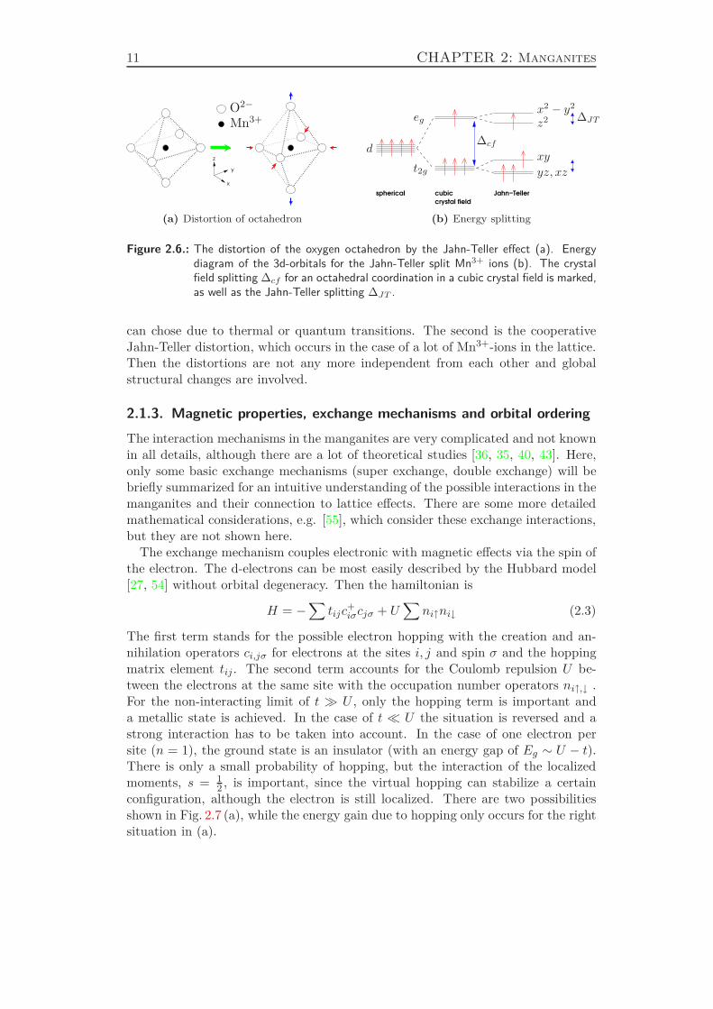
It has already been pointed out, that the symmetry of the orbitals within thecrystal has an important influence onto the resulting energy splitting. Here anothermechanism, the Jahn-Teller-distortion [29] driven by symmetry will be introduced.In Fig. 2.5 (b) the energy splitting of the eg and t2g orbitals has been shown. Accord-ing to Hund’s rule the electrons are filled such that a high spin state is achieved,since the Hund’s coupling is quite large in manganites. This means, that for aMn3+-ion the t2g orbitals are all filled with one electron and in the doubly degen-erate eg orbitals one electron has to be placed. This is demonstrated in Fig. 2.6.Normally the eg orbitals are degenerated, but in a certain crystal environment thepreference of one orbital can lead to a lowering of the energy.
Consider the situation in which the d3z2−r2 orbital points into z-direction, like inFig. 2.6 (a) and the dx2−y2 is lying in the plane of the octahedron. An elongationof the Mn-O-bond in the z-direction would favor the d3z2−r2 orbital, due to thedecreased Coulomb repulsion between the oxygen ions. At the same time theoctahedron becomes compressed within the xy-plane, which would enhance theCoulomb repulsion. The interplay between the energy lowering and the elasticstrain leads to an energy minimum for a certain distortion. This distortion does notaccount for the Mn4+-ion, since there is no such asymmetric occupation possible.
There are several possibilities of a Jahn-Teller distortion. The first is the dy-namical one, which appears, if there are several energy minima between the system
11 CHAPTER 2: Manganites
z
x
y
O2−
Mn3+
(a) Distortion of octahedron
Jahn−Tellerspherical
crystal field
cubic
d
eg
t2g
x2 − y2
z2
xy
yz, xz
∆cf
∆JT
(b) Energy splitting
Figure 2.6.: The distortion of the oxygen octahedron by the Jahn-Teller effect (a). Energydiagram of the 3d-orbitals for the Jahn-Teller split Mn3+ ions (b). The crystalfield splitting ∆cf for an octahedral coordination in a cubic crystal field is marked,as well as the Jahn-Teller splitting ∆JT .
can chose due to thermal or quantum transitions. The second is the cooperativeJahn-Teller distortion, which occurs in the case of a lot of Mn3+-ions in the lattice.Then the distortions are not any more independent from each other and globalstructural changes are involved.
2.1.3. Magnetic properties, exchange mechanisms and orbital ordering
The interaction mechanisms in the manganites are very complicated and not knownin all details, although there are a lot of theoretical studies [36, 35, 40, 43]. Here,only some basic exchange mechanisms (super exchange, double exchange) will bebriefly summarized for an intuitive understanding of the possible interactions in themanganites and their connection to lattice effects. There are some more detailedmathematical considerations, e.g. [55], which consider these exchange interactions,but they are not shown here.
The exchange mechanism couples electronic with magnetic effects via the spin ofthe electron. The d-electrons can be most easily described by the Hubbard model[27, 54] without orbital degeneracy. Then the hamiltonian is
H = −∑
tijc+iσcjσ + U
∑
ni↑ni↓ (2.3)
The first term stands for the possible electron hopping with the creation and an-nihilation operators ci,jσ for electrons at the sites i, j and spin σ and the hoppingmatrix element tij . The second term accounts for the Coulomb repulsion U be-tween the electrons at the same site with the occupation number operators ni↑,↓ .For the non-interacting limit of t ≫ U , only the hopping term is important anda metallic state is achieved. In the case of t ≪ U the situation is reversed and astrong interaction has to be taken into account. In the case of one electron persite (n = 1), the ground state is an insulator (with an energy gap of Eg ∼ U − t).There is only a small probability of hopping, but the interaction of the localizedmoments, s = 1
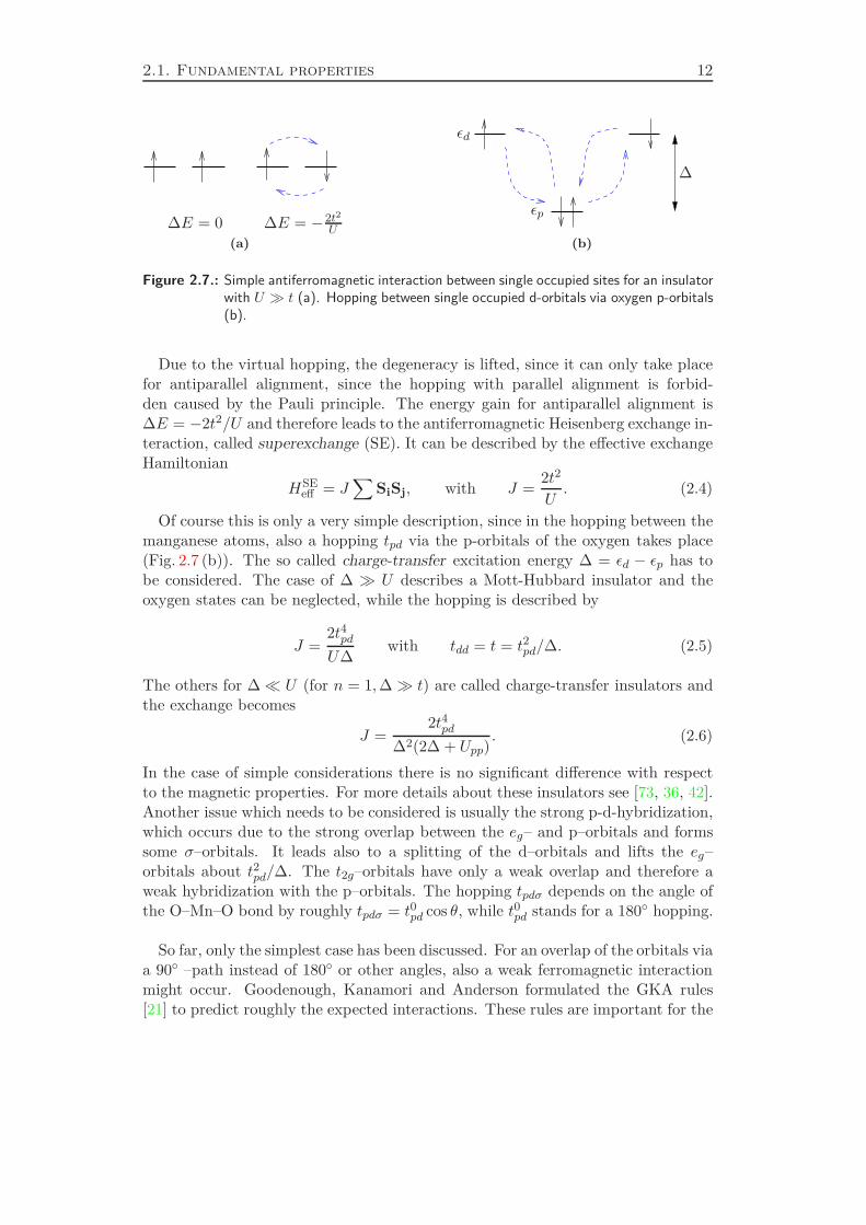
2 , is important, since the virtual hopping can stabilize a certainconfiguration, although the electron is still localized. There are two possibilitiesshown in Fig. 2.7 (a), while the energy gain due to hopping only occurs for the rightsituation in (a).
2.1. Fundamental properties 12
∆E = 0 ∆E = −2t2
U(a)
ǫd
ǫp
∆
(b)
Figure 2.7.: Simple antiferromagnetic interaction between single occupied sites for an insulatorwith U ≫ t (a). Hopping between single occupied d-orbitals via oxygen p-orbitals(b).
Due to the virtual hopping, the degeneracy is lifted, since it can only take placefor antiparallel alignment, since the hopping with parallel alignment is forbid-den caused by the Pauli principle. The energy gain for antiparallel alignment is∆E = −2t2/U and therefore leads to the antiferromagnetic Heisenberg exchange in-teraction, called superexchange (SE). It can be described by the effective exchangeHamiltonian
HSEeff = J
∑
SiSj, with J =2t2
U. (2.4)
Of course this is only a very simple description, since in the hopping between themanganese atoms, also a hopping tpd via the p-orbitals of the oxygen takes place(Fig. 2.7 (b)). The so called charge-transfer excitation energy ∆ = ǫd − ǫp has tobe considered. The case of ∆ ≫ U describes a Mott-Hubbard insulator and theoxygen states can be neglected, while the hopping is described by
J =2t4pdU∆
with tdd = t = t2pd/∆. (2.5)
The others for ∆≪ U (for n = 1,∆≫ t) are called charge-transfer insulators andthe exchange becomes
J =2t4pd
∆2(2∆ + Upp). (2.6)
In the case of simple considerations there is no significant difference with respectto the magnetic properties. For more details about these insulators see [73, 36, 42].Another issue which needs to be considered is usually the strong p-d-hybridization,which occurs due to the strong overlap between the eg– and p–orbitals and formssome σ–orbitals. It leads also to a splitting of the d–orbitals and lifts the eg–orbitals about t2pd/∆. The t2g–orbitals have only a weak overlap and therefore aweak hybridization with the p–orbitals. The hopping tpdσ depends on the angle ofthe O–Mn–O bond by roughly tpdσ = t0pd cos θ, while t0pd stands for a 180 hopping.
So far, only the simplest case has been discussed. For an overlap of the orbitals viaa 90 –path instead of 180 or other angles, also a weak ferromagnetic interactionmight occur. Goodenough, Kanamori and Anderson formulated the GKA rules[21] to predict roughly the expected interactions. These rules are important for the
13 CHAPTER 2: Manganites
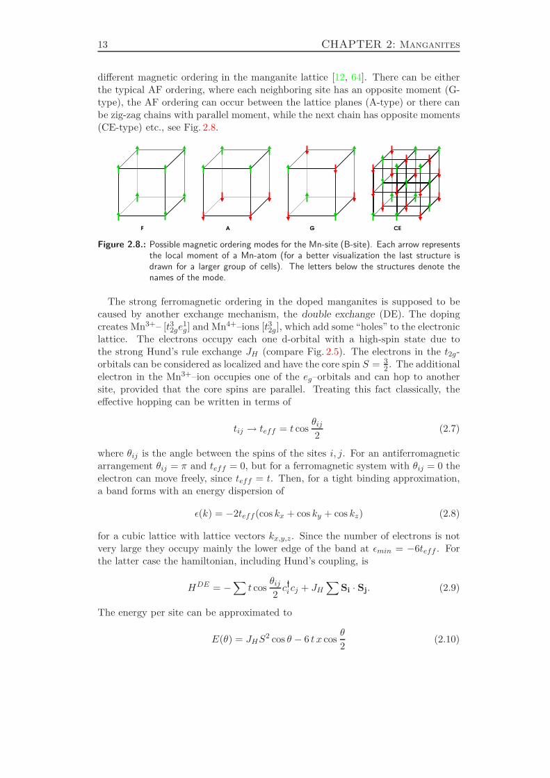
different magnetic ordering in the manganite lattice [12, 64]. There can be eitherthe typical AF ordering, where each neighboring site has an opposite moment (G-type), the AF ordering can occur between the lattice planes (A-type) or there canbe zig-zag chains with parallel moment, while the next chain has opposite moments(CE-type) etc., see Fig. 2.8.
G CEAF
Figure 2.8.: Possible magnetic ordering modes for the Mn-site (B-site). Each arrow representsthe local moment of a Mn-atom (for a better visualization the last structure isdrawn for a larger group of cells). The letters below the structures denote thenames of the mode.
The strong ferromagnetic ordering in the doped manganites is supposed to becaused by another exchange mechanism, the double exchange (DE). The dopingcreates Mn3+– [t32ge
1g] and Mn4+–ions [t32g], which add some “holes” to the electronic
lattice. The electrons occupy each one d-orbital with a high-spin state due tothe strong Hund’s rule exchange JH (compare Fig. 2.5). The electrons in the t2g-orbitals can be considered as localized and have the core spin S = 3
2 . The additionalelectron in the Mn3+–ion occupies one of the eg–orbitals and can hop to anothersite, provided that the core spins are parallel. Treating this fact classically, theeffective hopping can be written in terms of
tij → teff = t cosθij2
(2.7)
where θij is the angle between the spins of the sites i, j. For an antiferromagneticarrangement θij = π and teff = 0, but for a ferromagnetic system with θij = 0 theelectron can move freely, since teff = t. Then, for a tight binding approximation,a band forms with an energy dispersion of
ǫ(k) = −2teff (cos kx + cos ky + cos kz) (2.8)
for a cubic lattice with lattice vectors kx,y,z. Since the number of electrons is notvery large they occupy mainly the lower edge of the band at ǫmin = −6teff . Forthe latter case the hamiltonian, including Hund’s coupling, is
HDE = −∑
t cosθij2cicj + JH
∑
Si · Sj. (2.9)
The energy per site can be approximated to
E(θ) = JHS2 cos θ − 6 t x cosθ
2(2.10)
2.1. Fundamental properties 14
(x is, as given above, the doping level) with a minimum in θ of
cosθ
2=
32t
JHS2x. (2.11)
Above the critical value x > xc = 2/3JHS2/t a ferromagnetic ordering is estab-lished. The hopping here is different, compared to the Mott insulators, since noactivation energy is needed yielding a ferromagnetic state. It can be used to explainthe change of the magnetic ordering with doping and the occurrence of metallicitywith ferromagnetism.
The above discussed model is also referred as part of the one-orbital model [13],since only one orbital on each site was considered. It should be emphasized, thata lot of simplifications were made, to understand the basic mechanism. They candescribe some of the situations quite well, but in reality the systems are muchmore complex. For instance in the last considerations the Jahn-Teller splitting,the other ions or other orbitals and the bond angles between the d- and p-orbitalshave been neglected. Nevertheless these simple mechanisms give some insights intothe understanding of the physics in manganites. For instance, the competitionbetween antiferromagnetic (AF) and ferromagnetic (FM) ordering is revealed bythe exchange mechanisms. The idea of the CMR is, that the additional electrons(holes) from the doping can move through the crystal, but are influenced by thelocalized spins.
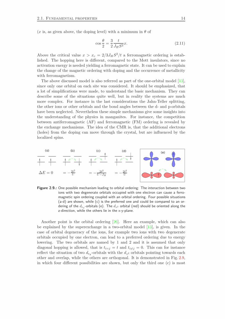
(a) (b) (c) (d)(e)
∆E = 0 = −2t2
U = −2t2
U= − 2t2
U−JH
Figure 2.9.: One possible mechanism leading to orbital ordering: The interaction between twoions with two degenerate orbitals occupied with one electron can cause a ferro-magnetic spin ordering coupled with an orbital ordering. Four possible situations(a-d) are shown, while (c) is the preferred one and could be compared to an or-dering of the deg -orbitals (e). The dz2 orbital (red) should be oriented along thez-direction, while the others lie in the x-y-plane.
Another point is the orbital ordering [26]. Here an example, which can alsobe explained by the superexchange in a two-orbital model [13], is given. In thecase of orbital degeneracy of the ions, for example two ions with two degenerateorbitals occupied by one electron, can lead to a preferred ordering due to energylowering. The two orbitals are named by 1 and 2 and it is assumed that onlydiagonal hopping is allowed, that is ti=j = t and ti6=j = 0. This can for instancereflect the situation of two deg -orbitals with the dz2 orbitals pointing towards eachother and overlap, while the others are orthogonal. It is demonstrated in Fig. 2.9,in which four different possibilities are shown, but only the third one (c) is most
15 CHAPTER 2: Manganites
probable for energetic reasons. Here, since the Hund’s coupling energy is gainedU ≫ JH , a weak ferromagnetic spin ordering (JH ≪ 1) is preferred together withthe orbital ordering. The latter occurs quite often in manganites and is thereforean important issue.
The one- and two-orbital models have been widely discussed [13, 14] and used formodel calculations within the physics of manganites. In these models already thedifferent influences of the Coulombic, antiferromagnetic and ferromagnetic interac-tions can be taken into account to form reasonable phase diagrams. On the otherhand, the situation is much more complex and it is difficult to separate the differentcontributions from each other. An example for an even more detailed analysis witha complex consideration of the electronic effects is the LDA+U method [7, 6] (local
density of states calculation, taking the Coulomb interaction into consideration)and also in combination with the DMFT (dynamical mean-field theory) method[47, 20, 30, 43].
2.1.4. Beyond the simple mechanisms: Polarons
The simple models, introduced so far, are usually not sufficient to explain thecomplex properties of the manganites. In particular, magnetic ordering can beobserved together with very different transport properties, like a FM state coupledtogether either with a metallic or insulating state, or an AF state which is metallic[4]. The radius of the ions used for doping, and the concomitant lattice distortionsdo not scale linearly with the resistivity [17]. Moreover the residual resistivitiesat low temperatures (T ∼= 4.2 K) are quite different. It is important to considerfurther mechanisms [50].
(a) (b) (c) (d)
eg electronMn3+
Mn3+
Mn4+O2−
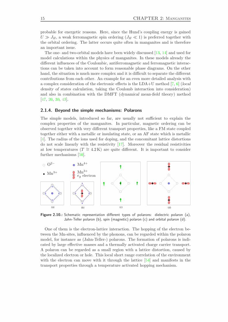
Figure 2.10.: Schematic representation different types of polarons: dielectric polaron (a),Jahn-Teller polaron (b), spin (magnetic) polaron (c) and orbital polaron (d).
One of them is the electron-lattice interaction. The hopping of the electron be-tween the Mn-sites, influenced by the phonons, can be regarded within the polaronmodel, for instance as (Jahn-Teller-) polarons. The formation of polarons is indi-cated by large effective masses and a thermally activated charge carrier transport.A polaron can be regarded as a small region with a lattice distortion, caused bythe localized electron or hole. This local short range correlation of the environmentwith the electron can move with it through the lattice [54] and manifests in thetransport properties through a temperature activated hopping mechanism.
2.2. Phase separation 16
There are different kinds of polarons: the dielectric, Jahn-Teller and spin andorbital polaron. The first is probably the most simplest case; due to the differentionic radii of differently charged ions (e.g. Mn4+ is smaller compared to Mn3+) adistortion can occur and the surrounding ions move towards the ion with smallerradius, as shown in Fig. 2.10 (a). Also a bound pair like a bipolaron or Zener polaroncan be formed [71, 18]. With the Jahn-Teller polaron a Jahn-Teller distortion isbound to the electron (hole), Fig. 2.10 (b). A magnetic or spin polaron (c) consistsof an electron with its spin and the surrounding, which is forced to have a parallelspin. The last one mentioned is the orbital polaron (d) [37], in which the orbitalstake on a specific orientation with respect to the electron (hole). Additionallyone differs between small and large polarons. The first is reduced to a single site,while the second describes an extension, which is larger than a lattice spacing.In manganites polarons were already seen experimentally, but are still an issue ofcontroversial discussions [1, 63, 32], since their role with respect to the transportis not finally clarified.
Above TC the activated transport behavior was very clearly associated with po-larons, since the resistivity followed an activated insulating like behavior with tem-perature, that is ρ ∼ exp(T0/T
1/4) [68]. Some papers report on the correlatedpolarons, observed by X-ray scattering or small angle neutron diffraction [16, 1, 39]For the low temperature metallic phase also indications of polarons are given –at least nearby the MIT – and discussed controversially [25]. The nature of thepolarons is not clear in detail, though a magnetic character is expected due to thelarge resistance changes around TC . At least some spin correlations were observedfor LCMO x = 0.3 [44] and Jahn-Teller polarons are indicated by the temperaturedependent anomalies in the lattice parameters around TC in various compoundswith x ≈ 0.3 [57]. Regarding the CMR effect, a magnetic field might suppressthe formation of polarons. It has also been reported, that the occurrence of corre-lated polarons can be attributed with an orthorhombic structure, but not with therhombohedral one [39].
2.2. Phase separation
From the DE mechanism (Sec. 2.1.3, Eq. 2.11) a kind of spin canting as a functionof doping x would be expected from the calculations. This is a controversial issue,since the compressibility is−d2E/dx2 < 0 and gives a hint for an instability towardsphase separation into FM metallic and AF insulating phases [33], which has beenalready shown experimentally. Also the two-orbital model gives hints for a phaseseparation with Jahn-Teller phonons taken into account [14].
In general, phase separation means that two competing phases coexist in thecompound. The different phases are characterized by different symmetry brakingpatterns, which are based on the spin, charge and orbital patterns in manganites.Here a ferromagnetic ordered phase competes with a spin antiferromagnetic orcharge ordered phase. In terms of manganites a phase does not necessarily consistof regions with a large number of electrons, which would be the case for a strictthermodynamic definition, but small clusters on the scale of the lattice spacing are
17 CHAPTER 2: Manganites
expected from the models, like for example the double exchange mechanism withlong range Coulomb interactions [13]. On the other hand experimentally also phaseseparation within the micrometer range were found.
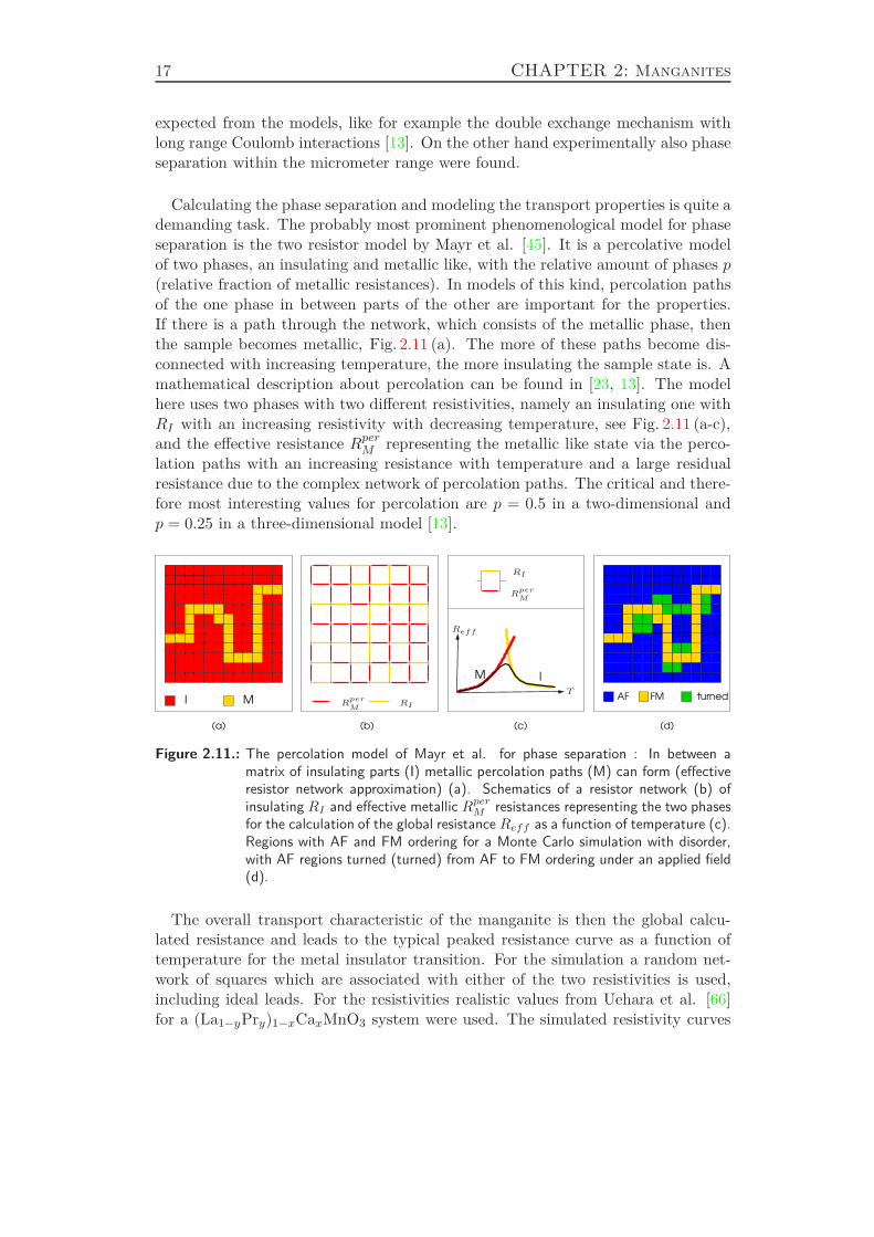
Calculating the phase separation and modeling the transport properties is quite ademanding task. The probably most prominent phenomenological model for phaseseparation is the two resistor model by Mayr et al. [45]. It is a percolative modelof two phases, an insulating and metallic like, with the relative amount of phases p(relative fraction of metallic resistances). In models of this kind, percolation pathsof the one phase in between parts of the other are important for the properties.If there is a path through the network, which consists of the metallic phase, thenthe sample becomes metallic, Fig. 2.11 (a). The more of these paths become dis-connected with increasing temperature, the more insulating the sample state is. Amathematical description about percolation can be found in [23, 13]. The modelhere uses two phases with two different resistivities, namely an insulating one withRI with an increasing resistivity with decreasing temperature, see Fig. 2.11 (a-c),and the effective resistance RperM representing the metallic like state via the perco-lation paths with an increasing resistance with temperature and a large residualresistance due to the complex network of percolation paths. The critical and there-fore most interesting values for percolation are p = 0.5 in a two-dimensional andp = 0.25 in a three-dimensional model [13].
turned
(a)
I M
(c)(b) (d)
AF FM
IM
RI
RI
Rper
M
Rper
M
Reff
T
Figure 2.11.: The percolation model of Mayr et al. for phase separation : In between amatrix of insulating parts (I) metallic percolation paths (M) can form (effectiveresistor network approximation) (a). Schematics of a resistor network (b) ofinsulating RI and effective metallic RperM resistances representing the two phasesfor the calculation of the global resistance Reff as a function of temperature (c).Regions with AF and FM ordering for a Monte Carlo simulation with disorder,with AF regions turned (turned) from AF to FM ordering under an applied field(d).
The overall transport characteristic of the manganite is then the global calcu-lated resistance and leads to the typical peaked resistance curve as a function oftemperature for the metal insulator transition. For the simulation a random net-work of squares which are associated with either of the two resistivities is used,including ideal leads. For the resistivities realistic values from Uehara et al. [66]for a (La1−yPry)1−xCaxMnO3 system were used. The simulated resistivity curves
2.2. Phase separation 18
qualitatively reflect the features of the MIT in manganites and also the insulatingbehavior over the full temperature range for constant p-values. The model de-scribes the situation sufficiently well, but could be improved in detail. This wasalso done by Mayr in fact, by varying p with the temperature and lead to a muchmore pronounced peak in the resistivity curves [45].
Another approach comes from Moreo et al. [52], in which disorder plays a crucialrole. Since the chemical doping alters the arrangements within the crystallinestructure with respect to bonding angles and distortions, also a correspondingdistribution of hopping matrix elements per site is expected, which leads to thedifferent regions. Moreo did some Monte Carlo simulations for the one– and two–orbital models in which some disorder was added. In the vicinity of a first-ordertransition, two different limits are interesting: For very strong disorder, clusterswith the size of a few lattice spacings were found, while in the case of weak disorderalso much larger clusters emerge, since too many interfaces would cost too muchenergy.
A similar result with respect to the domain sizes was obtained for a correspondingRandom Field Ising Model [52]. This model considers a hamiltonian of
H = −J∑
ij
Szi · Szj −∑
i
hi · Szi (2.12)
with the Ising variables Szi = +1,−1 arranged locally according to the randomfield hi. A system with only ferromagnetic interactions would prefer a uniformordering in this case with a first-order phase transition, but the added disorderparameter with the random field introduces small clusters into the system, even atlow temperatures T < TC . In this case the different regions have either spin up orspin down configuration and the main issue is to determine the cluster sizes withrespect to the disorder. The tendency of avoiding interfaces leads to a separationwith some clusters of varying size with h for small h, very small clusters for a largeh and huge clusters for small h/J . By switching on an external magnetic field H,some narrow parts of the spin down regions flip into spin up regions such that thelatter grow in size, Fig. 2.11 (d). The three dimensional case of this model shows adifferent result. Then a strong disorder would lead to large clusters while the weakdisorder tends to a more or less uniform state.
Another approach [59, 34] considers the phase-separation with especially regard-ing the Jahn-Teller distortions. It was found that there are less itinerant chargecarriers than the doping level would suggest. Like the other models mentioned sofar, the latter can mainly describe nanoscale phase-separation, which does not seemto be sufficient to describe the experimental results. Ahn et al. [3] consider straineffects within the sample and argue with an intrinsic elastic energy landscape caus-ing the micrometer scale multiphase separation. These considerations differ fromthe others with respect to the lattice degrees of freedom and electron-lattice cou-plings. It says that the phase separation is driven by the self-organization of elasticinhomogeneities. On the other hand, again a percolative result is obtained for theapplication of a magnetic field, which induces current paths in the sample. In this
19 CHAPTER 2: Manganites
model also the phases are distinct by a ferromagnetic metallic state (here denotedas the undistorted state) and an insulating (distorted) state, which produces a gapin the DOS. Another view is given by Milward et al. [51], who talks about elec-tronically soft phases. The Ginzburg-Landau theory is used with the magnetizationM(r) and the charge-orbital modulation ΨCO = A(r) exp [i(Qcr + Φ(r))]3 as orderparameters in the free energy density. The competition between the phases is givenhere between the magnetic order and charge modulation in new thermodynamicphases. Since the charge disproportionation between the Mn ions is not necessarilyunity, this model emphasizes a less localized charge-density wave picture.
In contrast to the other models, the latter considers a continuous phase transition,which would not show phase separation or a percolative picture of the phases.On the other hand the authors emphasize that a localized phase separation couldexist due to strain or disorder. Additionally the orbital ordering is described in asimple way, which does not involve different kinds of ordering. The other modelsintroduced so far, normally emanate from a first order, that is, a discontinuousphase transition. This question is still under debate and depending on the modeleither kind of the transition is possible. None of the models can predict a fullpicture of the manganites, because always some simplifications had to be made inorder to calculate or simulate the properties of the manganites. On the other handit is clear for everybody that there is a very strong interplay between the differentmechanisms in the manganites and neglecting a small part could already changethe picture. This is the reason why experiments considering this issue are stillnecessary to reveal more about the manganite physics. In the next section some ofthe experimental results with respect to LCMO will be given as a short overview.
2.3. The case of LCMO
In the following a short summary of the properties of LCMO is given. This includesthe basic properties and some newer results of intrinsic mechanisms in LCMO. Thepart about phase separation, for which already experiments and the respectivepublications exist, is displaced into the discussion with the results obtained in thiswork.
The peculiarity in LCMO is, that the ionic radius of Ca rCa∼= 1.14 Å is very
similar to that of La rLa∼= 1.172 Å [61] and a true solid solution is possible over
the entire doping range x. The phase diagram is given in Fig. 2.12 [11]. It is similarto La1−xSrxMnO3, which only exists up to x ≈ 0.6. The CMR can be observed forCa concentrations of 0.2 ≤ x ≤ 0.5, coupled to a transition from a ferromagneticmetal to a paramagnetic insulator.
The structure is normally orthorhombic for all doping levels below approximately700 K. In the very low doping (x < 0.2) and very high doping (x > 0.8) regions theproperties are less clear than in between, which might be associated to the role ofoxygen excess and deficiency observed for the end regions respectively. The largest
3r spatial coordinate, A amplitude of modulation, Qc = a∗/n wave vector commensurate withlattice with a∗ as reciprocal lattice vector, n integer, Φ phase incorporating structures withincommensurate periodicities.
2.3. The case of LCMO 20
1/8
3/8
4/8
5/8
7/8
CAF
FI
CO
FM
CO
AF CAF
0
0.5 1.0
100
200
300
Ca doping x
Tem
pe
ratu
re [
K]
0.250
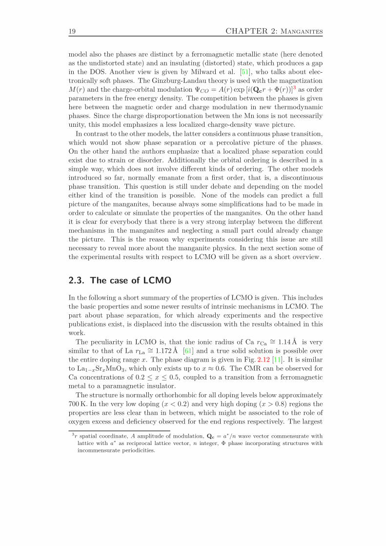
Figure 2.12.: Phase diagram from La1−xCaxMnO3. Numbers in blue denote special (com-mensurate) concentrations which show anomalies. The green line indicates thecomposition used for this work. FM: Ferromagnetic metal, FI: Ferromagnetic in-sulator, AF: Antiferromagnet, CAF: Canted antiferromagnet, CO: Charge/orbitalordered state. Redrawn according to [11].
regions show either a ferromagnetic metallic or an antiferromagnetic insulating lowtemperature phase, while the latter undergoes also a charge/orbital ordering tran-sition. Some special points can be seen in the phase diagram, marked by the bluenumbers, for commensurate electron concentrations. These might be the impor-tant hint to electron-lattice coupling in mixed-valent manganites. At these pointseither the critical temperature of the transition is largest (x = 1/8, 3/8, 5/8) or anabrupt change of the sample properties can be observed with a critical competitionbetween the neighboring ordering phenomena (x = 4/8, 7/8). Remarkably there isan asymmetry between hole and electron doping of the end members LaMnO3 andCaMnO3.
(a) (b) (c)
eg electronMn3+
Mn4+
Figure 2.13.: Charge and orbital ordering in La1−xCaxMnO3 with x = 0 (a), x = 1
2(b), x = 2
3
(c). The green bars mark the periodicity of the formed charge stripes.
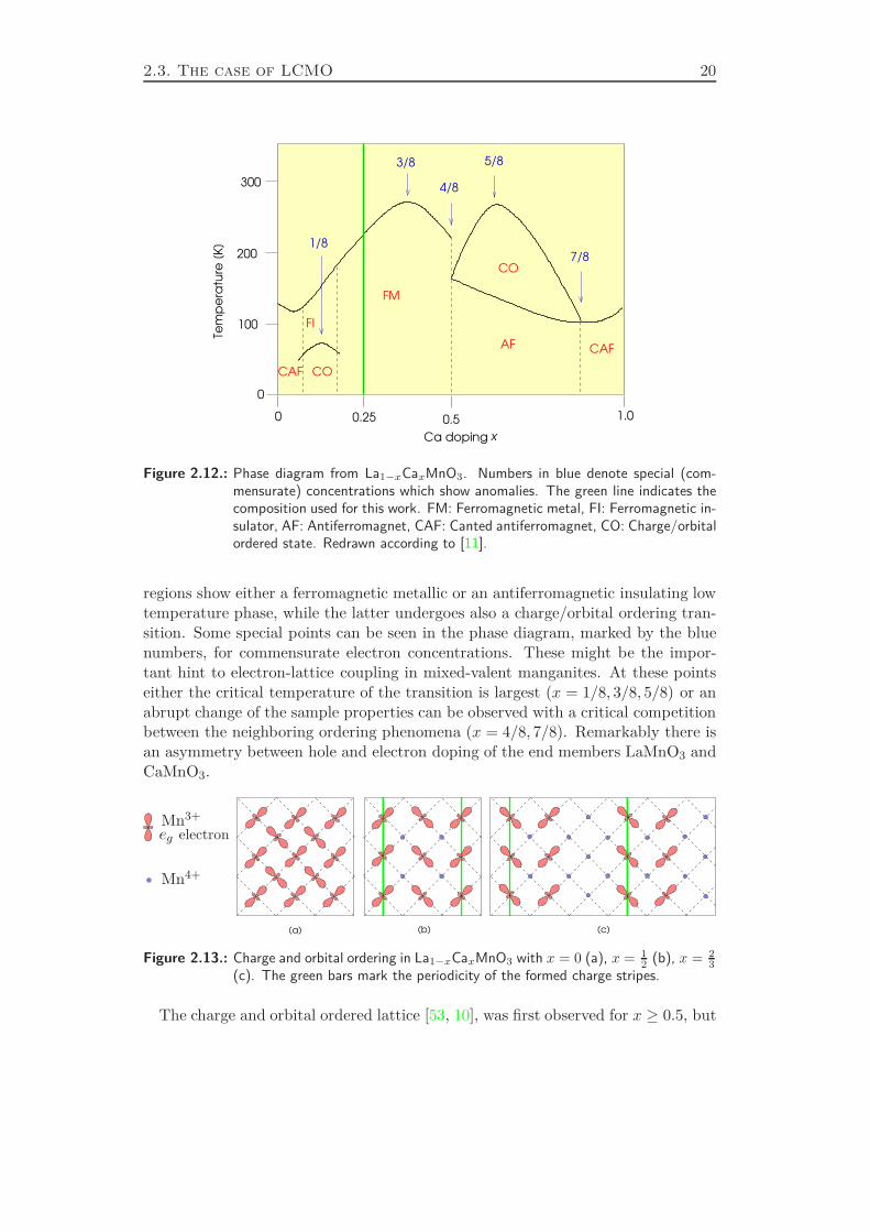
The charge and orbital ordered lattice [53, 10], was first observed for x ≥ 0.5, but
21 CHAPTER 2: Manganites
it can also occur in lower doping regions (see below). The eg–orbitals of the Mn3+–ions are arranged in a zigzag pattern with an adjacent number of Mn4+–ions inbetween. This ordering is shown in Fig. 2.13 for some commensurate compositions.For x = 0 the typical AF pattern of LaMnO3 is seen, but it is coupled to an orbitalordering of the eg orbitals. For the higher commensurate doping charge stripepatterns develop. In between these doping levels an interplay of the adjacent stripephases leads to a mixed pattern.
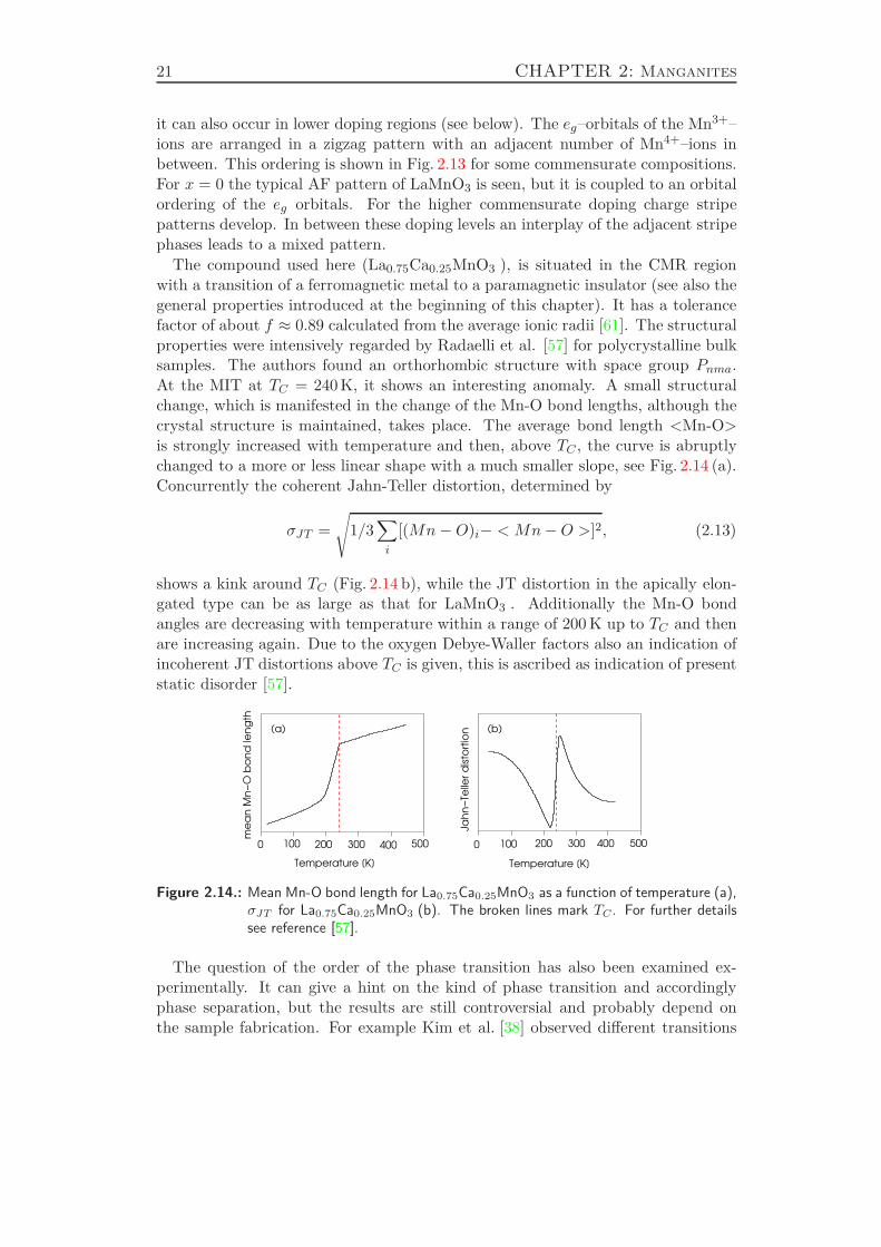
The compound used here (La0.75Ca0.25MnO3 ), is situated in the CMR regionwith a transition of a ferromagnetic metal to a paramagnetic insulator (see also thegeneral properties introduced at the beginning of this chapter). It has a tolerancefactor of about f ≈ 0.89 calculated from the average ionic radii [61]. The structuralproperties were intensively regarded by Radaelli et al. [57] for polycrystalline bulksamples. The authors found an orthorhombic structure with space group Pnma.At the MIT at TC = 240 K, it shows an interesting anomaly. A small structuralchange, which is manifested in the change of the Mn-O bond lengths, although thecrystal structure is maintained, takes place. The average bond length <Mn-O>is strongly increased with temperature and then, above TC , the curve is abruptlychanged to a more or less linear shape with a much smaller slope, see Fig. 2.14 (a).Concurrently the coherent Jahn-Teller distortion, determined by
σJT =√
1/3∑
i
[(Mn −O)i− < Mn−O >]2, (2.13)
shows a kink around TC (Fig. 2.14 b), while the JT distortion in the apically elon-gated type can be as large as that for LaMnO3 . Additionally the Mn-O bondangles are decreasing with temperature within a range of 200 K up to TC and thenare increasing again. Due to the oxygen Debye-Waller factors also an indication ofincoherent JT distortions above TC is given, this is ascribed as indication of presentstatic disorder [57].
300 400 500
(a) (b)
Temperature [K] Temperature [K]
200 300 400 5000 100
me
an
Mn
−O
bo
nd
len
gth
Jah
n−
Telle
r d
isto
rtio
n
0 100 200
Figure 2.14.: Mean Mn-O bond length for La0.75Ca0.25MnO3 as a function of temperature (a),σJT for La0.75Ca0.25MnO3 (b). The broken lines mark TC . For further detailssee reference [57].
The question of the order of the phase transition has also been examined ex-perimentally. It can give a hint on the kind of phase transition and accordinglyphase separation, but the results are still controversial and probably depend onthe sample fabrication. For example Kim et al. [38] observed different transitions
2.3. The case of LCMO 22
for La1−xCaxMnO3 polycrystalline samples and found a first-order transition forx = 0.33 expressed by a small discontinuity in the magnetization and volume ex-pansion, determined from the Clausius-Claperon equation. On the other hand thex = 0.4 sample showed a second-order transition for which the tricritical pointexponents were identified. This group claims that La1−xCaxMnO3 tends to a first-order transition for x < 0.4 and a second-order transition for x > 0.4. In con-trast to these observations Yanagisawa et al. [72] find a second-order transition inLa1−xCaxMnO3 with x = 0.35 by electron paramagnetic resonance. Souza et al.[62] analyzed the phase transition of La1−xCaxMnO3 with x = 0.3 as a polaroniccompound with a second-order transition. Again others report about a transitionsomewhere in between [56], which is neither exactly first or second order.
As already mentioned before, a simple mechanism is not sufficient to describethe manganites, which also applies to LCMO [15]. Also polarons might play animportant role. Some neutron scattering experiments on La1−xCaxMnO3 give hintsto polaron formation [44, 2]. The spin and charge dynamics leads to a formationof correlated polarons, which is consistent with the formation of charge stripes.An oxygen isotope effect (by replacing 16O by 18O) underlines the importance ofelectron lattice couplings.
Finally it should be mentioned that the properties observed for bulk samples donot necessarily have to be exactly the same as for thin films. Regarding thin filmsdeposited on a substrate the lattice mismatch between the crystalline substrate andthe thin film structure has to be taken into consideration as well. Due to stress orstrain in the film, the critical temperatures can be shifted and the residual resistivitycan be different, and the reduced size or film thickness effect the properties of thinfilms [49]. These issues will be discussed at the end of this work with respect ofthe samples used in this thesis.
23 Bibliography
Bibliography
[1] C. P. Adams, J. W. Lynn, Y. M. Mukovskii, A. A. Arsenov, and D. A. Shuly-atev. Phys. Rev. Lett., 85(18):3954, 2000.
[2] C. P. Adams, J. W. Lynn, V. N. Smolyaninova, A. Biswas, R. L. Greene,W. Ratcliff II, S.-W. Cheong, Y. M. Mukovskii, and D. A. shulyatev. Phys.
Rev. B, 70:134414, 2004.
[3] K. H. Ahn, T. Lookman, and A. R. Bishop. Nature, 428:401, 2004.
[4] T. Akimoto, Y. Manyama, Y. Moritomo, A. nakamura, K. Hirota,K. Oboyama, and M. Ohashi. Phys. Rev. B, 57:R5594, 1998.
[5] P. W. Anderson and H. Hasegawa. Phys. Rev., 100:675, 1955.
[6] V. I. Anisimov, F. Aryasetiawan, and A. I. Lichtenstein. J. Phys.: Cond. Mat.,9:767, 1997.
[7] V. I. Anisimov, J. Zaanen, and O. K. Anderson. Phys. Rev. B, 44:943, 1991.
[8] K. Chahara, T. Ohno, M. Kasai, and Y. Kozono. Appl. Phys. Lett., 63:1990,1999.
[9] A. Chainami, M. Mathew, and D. D. Sarma. Phys. Rev. B, 47:15397, 1993.
[10] C. H. Cheong, S.-W. Cheong, and H. Y. Hwang. J. Appl. Phys., 81:4326, 1997.
[11] S.-W. Cheong and H. Y. Hwang. Colossal-magnetoresistive oxides, chapter7. Ferromagnetism vs. Charge/Orbital Ordering. Gordon and Breach SciencePublisher, 200.
[12] J. M. D. Coey, M. Viret, and S. von Molnár. Adv. Phys., 48:167, 1999.
[13] E. Dagotto. Nanoscale Phase Separation and Colossal Magnetoresistance.Springer Verlag Berlin Heidelberg, 2003.
[14] E. Dagotto, T. Hotta, and A. Moreo. Phys. Rep., 344:1, 2001.
[15] P. Dai, J. A. Fernandez-Baca, E. W. Plummer, Y. Tomioka, and Y. Tokura.Phys. Rev. B, 64:224429, 2001.
[16] Pengcheng Dai, J. A. Fernandez-Baca, N. Wakabayashi, E. W. Plummer,Y. Tomioka, and Y. Tokura. Phys. Rev. Lett., 85(12):2553, 2000.
[17] F. Damay, A. Maignan, C. Martin, and B. Raveau. J. Appl. Phys, 81:1372,1997.
[18] A. Daoud-Aladine, J. Rodriguez-Carvajal, L. Pinsard-Gaudart, M. T.Fernández-Diaz, and A. Revcolevschi. Phys. Rev. Lett., 89:097205, 2002.
[19] P.-G. de Gennes. Phys. Rev., 118:141, 1960.
Bibliography 24
[20] A. Georges and G. Kotliar. Phys. Rev. B, 45:6479, 1992.
[21] J. B. Goodenough. Magnetism and chemical bond. Interscience Publishers,New York, 1963.
[22] L. P. Gor’kov and V. Z. Kresin. Phys. Rep., 400:149, 2004.
[23] G. Grimmelt. Percolation. Springer, 1999.
[24] R. Gross and A. Marx. Spinelektronik. Lecturenotes fromhttp://www.wmi.badw.de/teaching/Lecturenotes/, Walther-Meissner-Institut, Garching, 2004.
[25] Ch. Hartinger, F. Mayr, A. Loidl, and T. Kopp. Phys. Rev. B, 73:024408,2006.
[26] T. Hotta. Rep. Prog. Phys., 69:2061–2155, 2006.
[27] J. Hubbard. Electron correlations in narrow energy bands. Proc. Roy. Soc. A,276:238, 1963.
[28] M. Imada, A. Fujimori, and Y. Tokura. Rev. Mod. Phys., 70:1039, 1998.
[29] H. A. Jahn and E. Teller. Proc. Royal Soc. London A, 161:220, 1937.
[30] M. Jarrell. Phys. Rev. Lett., 69:168, 1992.
[31] G. H. Jonker. Physica, 22:707, 1956.
[32] Ch. Jooss, L. Wu, T. Beetz, R. F. Klie, M. Beleggia, M. A. Schofield,S. Schramm, J. Hoffmann, and Y. Zhu. Proc. Natl. Acad. Sci., 2007.
[33] M. Yu. Kagan, D. I. Khomskii, and M. V. Mostovoy. Eur. Phys. J. B, 12:217,1999.
[34] M. Yu Kagan and K. I. Kugel. Physics-Uspekhi, 44:553, 2001.
[35] D. Khomskii. Electronic structure, exchange and magnetism in oxides. InM. J. Thornton and M. Ziese, editors, Spin electronics, volume 569 of Lecture
notes in physics, 2001.
[36] D. Khomskii and G. Sawatzky. Solid State Comm., 102:87, 1997.
[37] R. Kilian and G. Khaliullin. Phys. Rev. B, 60:13458, 1999.
[38] D. Kim, B. Revaz, B. L. Zink, F. Hellman, J. J. Rhyne, and J. F. Mitchell.Phys. Rev. Lett., 89:227202, 2002.
[39] V. Kiryukhin, T. Y. Koo, H. Ishibashi, J. P. Hill, and S-W. Cheong. Phys.
Rev. B, 67(6):064421, 2003.
25 Bibliography
[40] E. Koch. Correlated electrons. In S. Blügel, Th. Brückel, and C. M. Schneider,editors, Magnetism goes Nano, volume 36 of Spring School of the Institute of
Solid State Research. Forschungszentrum Jülich GmbH, Institut für Festkör-perforschung, 2005.
[41] R. M. Kusters, J. Singleton, D. A. Keen, R. McGreevy, and W. Hayes. Physica
B, 155:362, 1989.
[42] A. I. Lichtenstein. Electronic structure of magnetic oxides. In P. H. Dederichs,P. Grünberg, and R. Hölzle, editors, Magnetische Schichtsysteme, volume 30of Spring School of the Institute of Solid State Research. ForschungszentrumJülich GmbH, Institut für Festkörperforschung, 1999.
[43] A. I. Lichtenstein. Electronic structure of complex oxides. In S. Blügel,Th. Brückel, and C. M. Schneider, editors, Magnetism goes Nano, volume 36of Spring School of the Institute of Solid State Research. ForschungszentrumJülich GmbH, Institut für Festkörperforschung, 2005.
[44] J. W. Lynn and C. P. Adams. J. Appl. Phys., 89:6846, 2001.
[45] M. Mayr, A. Moreo, J. A. Verges, J. Arispe, A. Feiguin, and E. Dagotto. Phys.
Rev. Lett., 86:135, 2001.
[46] M. McCormack, S. Jin, T. H. Tiefel, R.M. Fleming, and J.M. Phillips. Appl.
Phys. Lett., 64:3045, 1994.
[47] W. Metzner and D. Vollhardt. Phys. Rev. Lett., 62:324, 1989.
[48] H. P. Meyers. Introductory Solid State Physics. Taylor & Francis, 1997.
[49] A. J. Millis, T. Darling, and A. Migliori. J. Appl. Phys., 83:1588, 1998.
[50] A. J. Millis, P. B. Littlewood, and B. I. Shraiman. Phys. Rev. Lett., 74:5144,1995.
[51] G. C. Milward, M. J. Calderón, and P. B. Littlewood. Nature, 433:607, 2005.
[52] A. Moreo, M. Mayr, A. Feiguin, S. Yunoki, and E. Dagotto. Phys. Rev. Lett.,84, 2000.
[53] S. Mori, C. H. Chen, and S.-W. Cheong. Nature, 392:473, 1998.
[54] N. F. Mott. Metal insulator Transitions. Taylor & Francis, 1997.
[55] W. Nolting. Quantentheorie des Magnetismus, volume Teil 1 - Grundlagen.B. G. Teubner Stuttgart, 1986.
[56] P. Novák, M. Maryško, M. M. Savosta, and A. N. Ulyanov. Phys. Rev. B,60:6655, 1999.
[57] P. G. Radaelli, G. Iannone, M. Marezio, H. Y. Hwang, S.-W. Cheong, J. D.Jorgensen, and D. N. Argyriou. Phys. Rev. B, 56:8265, 1997.
Bibliography 26
[58] M. B. Salamon and M. Jaime. Rev. Mod. Phys., 73:583, 2001.
[59] A. O. Sboychakov, K. I. Kugel, and A. L. Rakhmanov. Phys. Rev. B,74:014401, 2006.
[60] C. W. Searle and S. T. Wang. Can. J. Phys., 47:2023, 1969.
[61] R. D. Shannon. Acta. Cryst., A 32:751, 1976.
[62] J. A. Souza, Y.-K. Yu, J. J. Neumeier, H. Terashita, and R. F. Jardim. Phys.
Rev. Lett., 94:207209, 2005.
[63] L. Sudheendra, V. Moshnyaga, E. D. Mishina, B. Damaschke, Th. Rasing, andK. Samwer. Phys. Rev. B, 75:172407, 2007.
[64] Y. Tokura, editor. Colossal-magnetoresistive oxides. Gordon and Breach Sci-ence Publishers, 2000.
[65] Y. Tokura. Rep. Prog. Phys, 69:797, 2006.
[66] M. Uehara, S. Mori, C. H. Chen, and S.-W. Cheong. Nature, 399:560, 1999.
[67] J. H. van Santen and G. H. Jonker. Physica, 16:599, 1950.
[68] M. Viret, L. Ranno, and J. M. D. Coey. Phys. Rev. B, 55(13):8067, 1997.
[69] R. von Helmolt, J. Wecker, B. Holzapfel, L. Schultz, and K. Samwer. Phys.
Rev. Lett., 71:2331, 1993.
[70] E. O. Wollan and W. C. Koehler. Phys. Rev., 100:545, 1955.
[71] L. Wu, R. F. Klie, Y. Zhu, and Ch. Jooss. Phys. Rev. B, 76:174210, 2007.
[72] O. Yanagisawa, M. Izumi, K.-H. Huang, W.-Z. Hu, Y. Shen, K. Nakanishi,Y. Takahashi, and H. Nojima. J. Magn. Magn. Mat., 211:254, 2000.
[73] J. Zaanen, G. A. Sawatzky, and J. Allen. Phys. Rev. Lett., 55:418, 1985.
[74] C. Zener. Phys. Rev., 82:403, 1951.
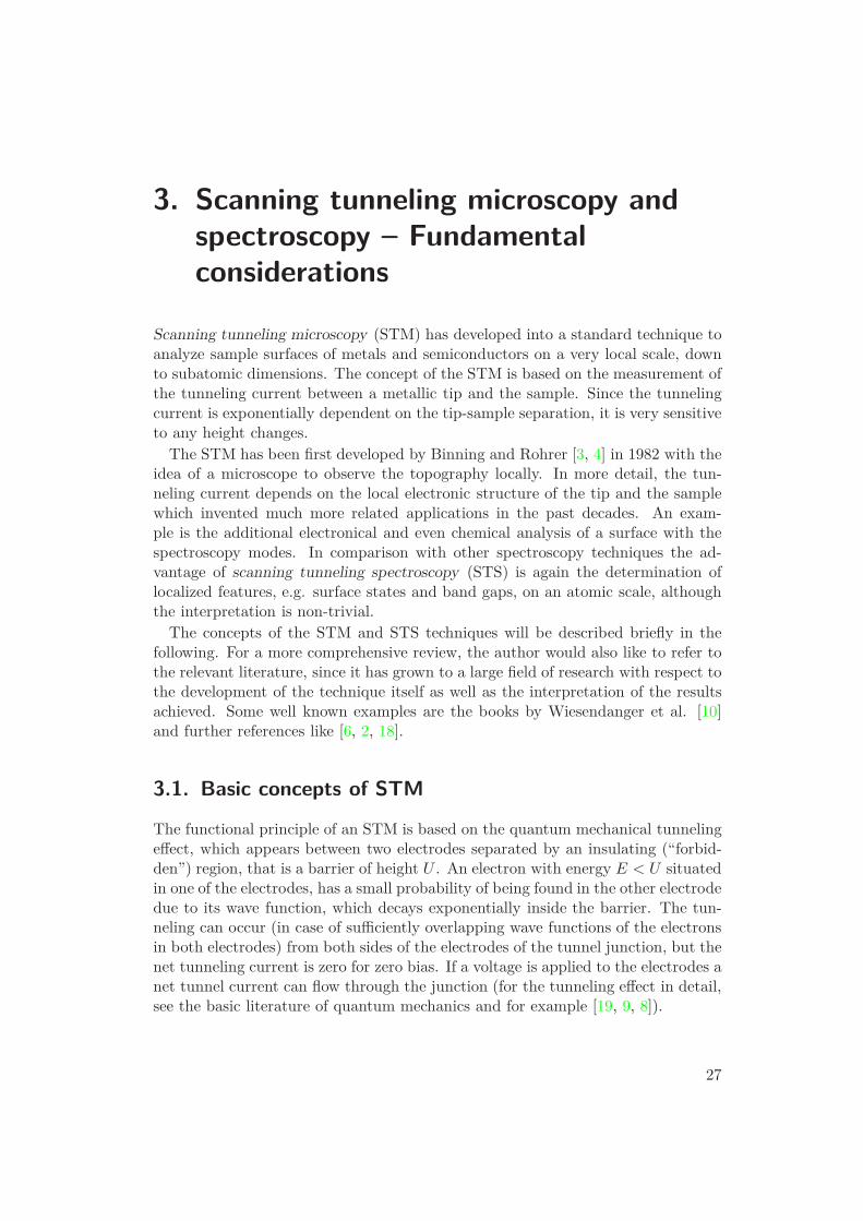
3. Scanning tunneling microscopy andspectroscopy – Fundamentalconsiderations
Scanning tunneling microscopy (STM) has developed into a standard technique toanalyze sample surfaces of metals and semiconductors on a very local scale, downto subatomic dimensions. The concept of the STM is based on the measurement ofthe tunneling current between a metallic tip and the sample. Since the tunnelingcurrent is exponentially dependent on the tip-sample separation, it is very sensitiveto any height changes.
The STM has been first developed by Binning and Rohrer [3, 4] in 1982 with theidea of a microscope to observe the topography locally. In more detail, the tun-neling current depends on the local electronic structure of the tip and the samplewhich invented much more related applications in the past decades. An exam-ple is the additional electronical and even chemical analysis of a surface with thespectroscopy modes. In comparison with other spectroscopy techniques the ad-vantage of scanning tunneling spectroscopy (STS) is again the determination oflocalized features, e.g. surface states and band gaps, on an atomic scale, althoughthe interpretation is non-trivial.
The concepts of the STM and STS techniques will be described briefly in thefollowing. For a more comprehensive review, the author would also like to refer tothe relevant literature, since it has grown to a large field of research with respect tothe development of the technique itself as well as the interpretation of the resultsachieved. Some well known examples are the books by Wiesendanger et al. [10]and further references like [6, 2, 18].
3.1. Basic concepts of STM
The functional principle of an STM is based on the quantum mechanical tunnelingeffect, which appears between two electrodes separated by an insulating (“forbid-den”) region, that is a barrier of height U . An electron with energy E < U situatedin one of the electrodes, has a small probability of being found in the other electrodedue to its wave function, which decays exponentially inside the barrier. The tun-neling can occur (in case of sufficiently overlapping wave functions of the electronsin both electrodes) from both sides of the electrodes of the tunnel junction, but thenet tunneling current is zero for zero bias. If a voltage is applied to the electrodes anet tunnel current can flow through the junction (for the tunneling effect in detail,see the basic literature of quantum mechanics and for example [19, 9, 8]).
27
3.1. Basic concepts of STM 28
In the one-dimensional case of the semi-classical WKB1 approximation, the re-sulting probability of for example an electron of the tip being localized in the sampleat position z is
|Ψ(z)|2 = |Ψ(0)|2 e−2κz (3.1)
with
κ =√
me~2
(Φt + Φs − eV ), (3.2)
in which me is the electron mass and Φs/t are the work functions for the twoelectrodes. It is evident that the tunneling probability I ∝ |Ψ(z)|2 is exponentiallydependent on the tip-sample separation, (lying in the z-direction)
I ∝ e−κz. (3.3)
Taking reasonable values for a metallic tunneling system with work functions about4-5 eV [11], then κ ≈ 10 nm−1, which means that a change in z of about 0.1 nmalters the tunneling probability by about one order of magnitude.
In the STM the tunneling system is built out of a sharp metallic tip and thesample as electrodes and the (air or vacuum) gap between both as the tunnelingbarrier. Since our microscope was operated under ultra high vacuum (UHV) con-ditions, here only the vacuum tunneling through a vacuum gap is of interest. Viascanning the tip in x − y−direction above the surface, the local variation of thetunnel current is used in an STM to image the surface or the electronic propertiesof the surface due to its exponentially dependence I(z). Ideally, it is usually as-sumed that the tunneling current flows between the outermost apex atom of thetip and the sample surface atoms leading to a highly corrugated tunneling currentdistribution and therefore atomic resolution can be achieved. For a schematic viewsee Fig. 3.1, the technical realization is described in Chap. 5. The materials probedneed to be metallic or semiconducting. At first, for the interpretation of the STMmeasurements it is important to understand, which parameters enter the tunnelingequation.
The tunnel current between the sample (s) and the tip (t) depends on theirelectronic structure, which can be locally different. The diagram in Fig. 3.2 demon-strates the tunneling situation. Electrons can tunnel from each side of the barrier,but with a bias V applied a net tunneling current towards the lower potential sideis flowing. (In the convention used here, a positive voltage applied to the sam-ple means, that the Fermi energy of the tip EFt is increased with respect to theFermi energy of the sample EFs .) Electrons can only tunnel from occupied statesof the one electrode to appropriate empty states of the other electrode. Fig. 3.2only shows the simple picture for T = 0, the filling of the states is sharply limitedby the Fermi energy EF . For higher temperatures this border is broadened, andthe occupation probability of a state is described by the Fermi-Dirac distributionfunction
f(E) = (1 + exp [E/kBT ])−1. (3.4)1WKB means Wentzel-Kramers-Brillouin-Jeffreys approximation.
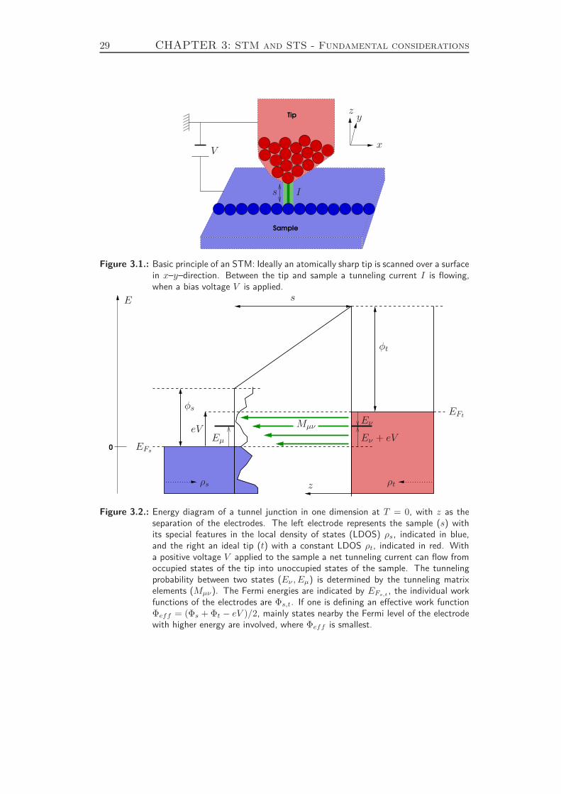
29 CHAPTER 3: STM and STS - Fundamental considerations
Tip
Sample
z
x
y
s I
V
Figure 3.1.: Basic principle of an STM: Ideally an atomically sharp tip is scanned over a surfacein x–y–direction. Between the tip and sample a tunneling current I is flowing,when a bias voltage V is applied.
0
φs
φt
EFs
EFtMµν
ρs ρt
s
z
eV
E
Eµ
Eν
Eν + eV
Figure 3.2.: Energy diagram of a tunnel junction in one dimension at T = 0, with z as theseparation of the electrodes. The left electrode represents the sample (s) withits special features in the local density of states (LDOS) ρs, indicated in blue,and the right an ideal tip (t) with a constant LDOS ρt, indicated in red. Witha positive voltage V applied to the sample a net tunneling current can flow fromoccupied states of the tip into unoccupied states of the sample. The tunnelingprobability between two states (Eν , Eµ) is determined by the tunneling matrixelements (Mµν). The Fermi energies are indicated by EFs,t , the individual workfunctions of the electrodes are Φs,t. If one is defining an effective work functionΦeff = (Φs + Φt − eV )/2, mainly states nearby the Fermi level of the electrodewith higher energy are involved, where Φeff is smallest.
3.1. Basic concepts of STM 30
Here the energies are given with respect to the Fermi energy. The total current isgiven by the sum over all possible states for an approximation with independentelectrodes. For example electrons from occupied states of the tip (with ft(Eν) andindex ν) can tunnel into unoccupied states of the sample (with [1 − fs(Eµ)] andindexed by µ). Taking a current into both directions into account the net tunnelingcurrent is:
I =4πe~
∑
µν
f(Eν) [1− f(Eµ)]− f(Eµ) [1− f(Eν)]
·|Mµν |2 · δ(Eµ − (Eν + eV )) (3.5)
=4πe~
∑
µν
[f(Eν)− f(Eµ)] · |Mµν |2 · δ(Eµ − Eν − eV ). (3.6)
The energies Eµ, Eν are given with respect to the Fermi energies EFs , EFt respec-tively, which is shown in Fig. 3.2 by the marked arrows. This case describes elastictunneling without any scattering and energy losses. Both states involved have thesame energy, denoted by the δ-function.2 Mµν are the tunneling matrix elements.They connect the wave functions (Ψsµ and Ψtν) of the electrons of both electrodesand describe the tunneling probability between states µ and ν.
The tunneling current is determined by summing over all possible states. Insteadof considering the states itself, it is beneficial to consider the density of states
(DOS) ρ(E) at an energy E. With this concept and changing the summation intoan integration (for a sufficiently large number of states involved) the tunnelingequation (Eq. 3.6) becomes
I =4πe~
+∞∫
−∞
dǫ [ft(ǫ− eV )− fs(ǫ)] · ρt(ǫ− eV )ρs(ǫ) · |M(ǫ, ǫ− eV )|2. (3.7)
The energies are given with respect to the Fermi energy of the electrodes.Bardeen [1] formulated a way to describe the tunneling matrix elements from a
many particle point of view by perturbation theory. Its modified approximationleads to
Mµν = − ~2
2m
∫
dS(
Ψ∗ν∇Ψµ −Ψ∗µ∇Ψν)
. (3.8)
The integration takes place over a surface S in between the electrodes within thebarrier. The dimension of the element is energy. It is justifiable to assume thematrix elements to be nearly constant in the regime of small bias voltage (eV ≪ Φand eV ≪ EF ). Physically the matrix element corresponds to the energy loweringcaused by the overlap of the wave functions.
The most difficult task is to determine the matrix elements without knowingexactly the properties of the tip and the sample, since they depend on the exactpositions of the atoms in space and the respective wave functions are energy de-pendent. Ideally the DOS of the tip would be constant, since one is only interested
2Mathematically the δ-function is not absolutely correct in the sum, but it is often used for abetter understanding.
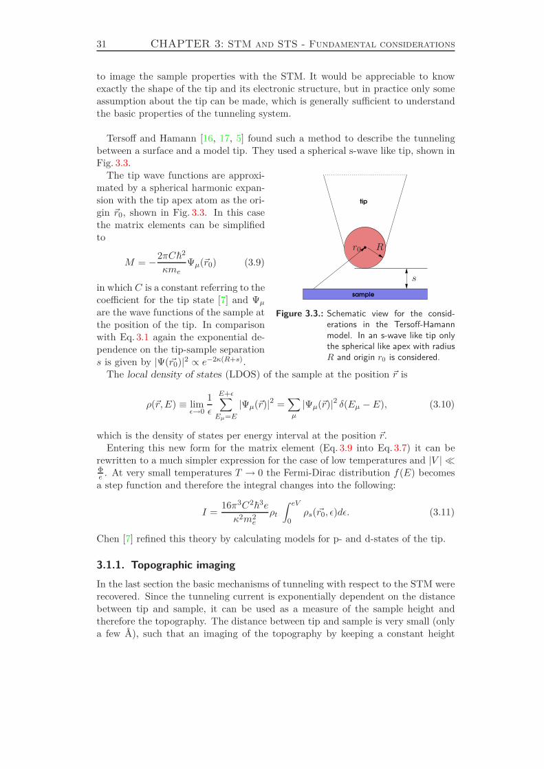
31 CHAPTER 3: STM and STS - Fundamental considerations
to image the sample properties with the STM. It would be appreciable to knowexactly the shape of the tip and its electronic structure, but in practice only someassumption about the tip can be made, which is generally sufficient to understandthe basic properties of the tunneling system.
Tersoff and Hamann [16, 17, 5] found such a method to describe the tunnelingbetween a surface and a model tip. They used a spherical s-wave like tip, shown inFig. 3.3.
The tip wave functions are approxi-
sample
tip
s
Rr0
Figure 3.3.: Schematic view for the consid-erations in the Tersoff-Hamannmodel. In an s-wave like tip onlythe spherical like apex with radiusR and origin r0 is considered.
mated by a spherical harmonic expan-sion with the tip apex atom as the ori-gin ~r0, shown in Fig. 3.3. In this casethe matrix elements can be simplifiedto
M = −2πC~2
κmeΨµ(~r0) (3.9)
in which C is a constant referring to thecoefficient for the tip state [7] and Ψµare the wave functions of the sample atthe position of the tip. In comparisonwith Eq. 3.1 again the exponential de-pendence on the tip-sample separations is given by |Ψ(~r0)|2 ∝ e−2κ(R+s).
The local density of states (LDOS) of the sample at the position ~r is
ρ(~r,E) ≡ limǫ→0
1ǫ
E+ǫ∑
Eµ=E
|Ψµ(~r)|2 =∑
µ
|Ψµ(~r)|2 δ(Eµ − E), (3.10)
which is the density of states per energy interval at the position ~r.Entering this new form for the matrix element (Eq. 3.9 into Eq. 3.7) it can be
rewritten to a much simpler expression for the case of low temperatures and |V | ≪Φe . At very small temperatures T → 0 the Fermi-Dirac distribution f(E) becomesa step function and therefore the integral changes into the following:
I =16π3C2
~3e
κ2m2e
ρt
∫ eV
0ρs(~r0, ǫ)dǫ. (3.11)
Chen [7] refined this theory by calculating models for p- and d-states of the tip.
3.1.1. Topographic imaging
In the last section the basic mechanisms of tunneling with respect to the STM wererecovered. Since the tunneling current is exponentially dependent on the distancebetween tip and sample, it can be used as a measure of the sample height andtherefore the topography. The distance between tip and sample is very small (onlya few Å), such that an imaging of the topography by keeping a constant height
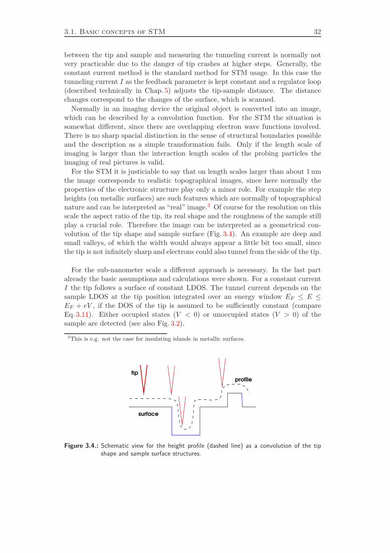
3.1. Basic concepts of STM 32
between the tip and sample and measuring the tunneling current is normally notvery practicable due to the danger of tip crashes at higher steps. Generally, theconstant current method is the standard method for STM usage. In this case thetunneling current I as the feedback parameter is kept constant and a regulator loop(described technically in Chap. 5) adjusts the tip-sample distance. The distancechanges correspond to the changes of the surface, which is scanned.
Normally in an imaging device the original object is converted into an image,which can be described by a convolution function. For the STM the situation issomewhat different, since there are overlapping electron wave functions involved.There is no sharp spacial distinction in the sense of structural boundaries possibleand the description as a simple transformation fails. Only if the length scale ofimaging is larger than the interaction length scales of the probing particles theimaging of real pictures is valid.
For the STM it is justiciable to say that on length scales larger than about 1 nmthe image corresponds to realistic topographical images, since here normally theproperties of the electronic structure play only a minor role. For example the stepheights (on metallic surfaces) are such features which are normally of topographicalnature and can be interpreted as “real” image.3 Of course for the resolution on thisscale the aspect ratio of the tip, its real shape and the roughness of the sample stillplay a crucial role. Therefore the image can be interpreted as a geometrical con-volution of the tip shape and sample surface (Fig. 3.4). An example are deep andsmall valleys, of which the width would always appear a little bit too small, sincethe tip is not infinitely sharp and electrons could also tunnel from the side of the tip.
For the sub-nanometer scale a different approach is necessary. In the last partalready the basic assumptions and calculations were shown. For a constant currentI the tip follows a surface of constant LDOS. The tunnel current depends on thesample LDOS at the tip position integrated over an energy window EF ≤ E ≤EF + eV , if the DOS of the tip is assumed to be sufficiently constant (compareEq. 3.11). Either occupied states (V < 0) or unoccupied states (V > 0) of thesample are detected (see also Fig. 3.2).
3This is e.g. not the case for insulating islands in metallic surfaces.
profile
surface
tip
Figure 3.4.: Schematic view for the height profile (dashed line) as a convolution of the tipshape and sample surface structures.

33 CHAPTER 3: STM and STS - Fundamental considerations
Now, one could take images at different voltages to observe different spacialfeatures of the electronic structure of the sample. This was done for instance onGaAs(110) [14], but it is not always as easy as in this example, where the valencestates and conduction states appear quite distinct from each other. Another methodwould be the tunneling spectroscopy, which is described next.
3.2. Spectroscopy
Scanning tunneling spectroscopy is a very powerful tool used with the STM. Thereare several methods to do spectroscopic measurements (the fixed separation orvariable separation I(V ) modes or a constant resistance mode [18]), but mainlythe determination of the current-voltage characteristics at a constant tip-sampleseparation is performed. With this technique special features in the LDOS can bedetermined. The spectroscopy data is taken by stopping the scanning and holdingthe tip at a constant height above a point of the sample, while the feedback loopis switched off. In order to measure the tunnel current as a function of the samplebias I(V ), the bias voltage is then changed (see also Chap. 5).
In Eq. 3.7 an expression for the tunneling current I is given. For a sufficientlysmall sample bias (eV ≪ Φt,Φs) the matrix elements M can be approximatedas being constant. The tunnel current I can then be expressed by the simplifiedexpression
I ∝∞∫
−∞
dǫ ρs(ǫ)ρt(ǫ− eV ) (ft(ǫ− eV )− fs(ǫ)) . (3.12)
Its derivative is
∂I
∂V
∣
∣
∣
∣
V0
∝∞∫
−∞
dǫ[
−ρs(ǫ)ρ′t(ǫ− eV0)ft(ǫ− eV0)
−ρs(ǫ)ρt(ǫ− eV0)f ′t(ǫ− eV0)
+ ρs(ǫ)ρ′t(ǫ− eV0)fs(ǫ)]
(3.13)
with the partial derivative of the DOS
ρ′ =∂ρ
∂ǫ(3.14)
and the derivative f ′(ǫ) of the Fermi-Dirac distribution function. (Here, for areversed bias the indices for the tip and sample could be exchanged, since thetunneling equation is symmetric.)
It is now assumed that ρ′t ≡ 0 corresponding to a constant DOS of the tip, thenonly the second term in Eq. 3.13 remains. For T → 0, the Fermi-Dirac distributionbecomes a step function f(ǫ)|kBT→0 = Θ(ǫ) and its derivative is a δ−function,therefore
∂I
∂V
∣
∣
∣
∣
V0
∝ ρteV∫
0
dǫ ρs(ǫ)δ(ǫ − eV0) = ρt · ρs(eV0). (3.15)
3.2. Spectroscopy 34
This equation shows that within the made assumptions ∂I/∂V is proportional tothe DOS of the tip and sample. Since ρt is supposed to be constant for these con-siderations, changes in ∂I/∂V at a given V0 correspond to changes in the DOS ofthe sample for the corresponding energy.
So far only the case of low temperatures was considered, which does not applyfor the measurements taken within this work. The general idea remains valid forhigher temperatures, that is, the proportionalities are not changed in principle.At higher temperatures the Fermi-Dirac distribution becomes less sharp and thetransition from occupied to unoccupied states around EF is much broader. Fromits derivative
f ′(ǫ) =∂f
∂ǫ=
− exp(ǫ/kBT )
kBT [1 + exp(ǫ/kBT )]2=
12kBT
· 1cosh2(ǫ/2kBT )
. (3.16)
the energy broadening can be estimated for finite temperatures. The derivative∂f/∂ǫ is a peak function. To estimate the temperature related broadening of theline width of spectroscopic features, a sample with an infinitely sharp δ−peak likefeature in the DOS ρs = Aδ(ǫ − ǫ0) is considered [15]. With Eq. 3.13 (again for aconstant DOS of the tip)
∂I
∂V
∣
∣
∣
∣
V0
∝∞∫
−∞
dǫ δ(ǫ− ǫ0) f ′t(ǫ− eV0) (3.17)
the energy broadening by the convolution of ρs with f ′(ǫ) of Eq. 3.16 leads to:
∂I
∂V
∣
∣
∣
∣
V0
∝ ρt ·1kBT· 1[
cosh(
ǫ0−eV02kBT
)]2 . (3.18)
The latter4 is a peaked function with its maximum at ǫ0 = eV0. The full widthat half maximum (FWHM) can be determined by a Gaussian approximation toabout FWHM 2σ ≈ 3.2 kBT/e, which is the minimum separation to resolve twosuch peaks. Therefore an energy resolution of about ∆E ≈ 100 meV is possible fora temperature of 300 K.
4Remarkably, only the temperature of the tip enters in this simplified consideration. Generally(and also in the case of this work) both, tip and sample, have the same temperature andthermoelectric voltages [13, 12] between tip and sample can be excluded.
35 Bibliography
Bibliography
[1] J. Bardeen. Phys. Rev. Lett., 6:57, 1961.
[2] G. Binning and H. Rohrer. Scanning tunneling microscopy – from birth toadolescence. Rev. Mod. Phys., 59:615, 1987.
[3] G. Binning, H. Rohrer, Ch. Gerber, and E. Weibel. Appl. Phys. Lett., 40:178,1981.
[4] G. Binning, H. Rohrer, Ch. Gerber, and E. Weibel. Phys. Rev. Lett., 49:57,1982.
[5] S. Blügel. Theorie der Rastertunnelmikroskopie, volume 29. Ferienkurs derFestkörperphysik, Physik der Nanostrukturen, chapter A3. Institut für Fes-tkörperforschung, Forschungszentrum Jülich, 1998.
[6] Dawn. A. Bonnell, editor. Scanning Tunneling Microscopy and Spectroscopy.VCH Publishers, Inc., 1993.
[7] C. J. Chen. Phys. Rev. B, 42:8841, 1990.
[8] C. Julian Chen. Introduction to Scanning Tunneling Microscopy. Oxford Uni-versity Press, 1993.
[9] C. B. Duke. Tunneling in solids. Academic Press, Inc., 1969.
[10] H.-J. Güntherodt and R. Wiesendanger, editors. Scanning Tunneling mi-
croscopy, volume I-III of Springer Series in Surface Science. Springer-Verlag,1992.
[11] H. B. Michaelson. J. Appl. Phys., 48:4729, 1977.
[12] M. A. Schneider, M. Wenderoth, K. J. Engel, M. A. Rosentreter, A. J. Heinrich,and R. G. Ulbrich. Appl. Phys. A., 66:S161, 1998.
[13] J. A. Støveng and P. Lipavský. Phys. Rev. B, 42:9214, 1990.
[14] J. Stroscio, R. Feenstra, and A. Fein. Phys. Rev. Lett., 57:2579, 1986.
[15] Markus Ternes. Scanning tunneling spectroscopy at the single atom scale. PhDthesis, École Polytechnique Fédérale de Lausanne, 2006.
[16] J. Tersoff and D. R. Hamann. Phys. Rev. Lett., 50:1998, 1983.
[17] J. Tersoff and D. R. Hamann. Phys. Rev. B, 31:805, 1985.
[18] L. E. C. van de Leemput and H. van Kempen. Rep. Prog. Phys., 55:1165,1992.
[19] E. L. Wolf. Principles of electron tunneling spectroscopy. Oxford UniversityPress, 1985.

Bibliography 36
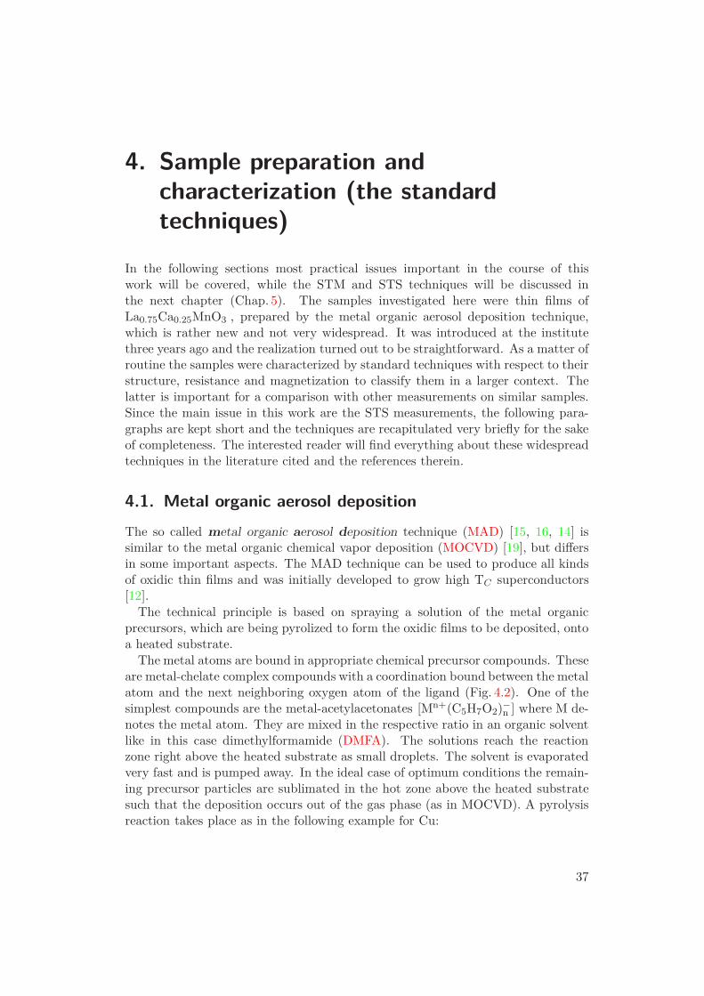
4. Sample preparation andcharacterization (the standardtechniques)
In the following sections most practical issues important in the course of thiswork will be covered, while the STM and STS techniques will be discussed inthe next chapter (Chap. 5). The samples investigated here were thin films ofLa0.75Ca0.25MnO3 , prepared by the metal organic aerosol deposition technique,which is rather new and not very widespread. It was introduced at the institutethree years ago and the realization turned out to be straightforward. As a matter ofroutine the samples were characterized by standard techniques with respect to theirstructure, resistance and magnetization to classify them in a larger context. Thelatter is important for a comparison with other measurements on similar samples.Since the main issue in this work are the STS measurements, the following para-graphs are kept short and the techniques are recapitulated very briefly for the sakeof completeness. The interested reader will find everything about these widespreadtechniques in the literature cited and the references therein.
4.1. Metal organic aerosol deposition
The so called metal organic aerosol deposition technique (MAD) [15, 16, 14] issimilar to the metal organic chemical vapor deposition (MOCVD) [19], but differsin some important aspects. The MAD technique can be used to produce all kindsof oxidic thin films and was initially developed to grow high TC superconductors[12].
The technical principle is based on spraying a solution of the metal organicprecursors, which are being pyrolized to form the oxidic films to be deposited, ontoa heated substrate.
The metal atoms are bound in appropriate chemical precursor compounds. Theseare metal-chelate complex compounds with a coordination bound between the metalatom and the next neighboring oxygen atom of the ligand (Fig. 4.2). One of thesimplest compounds are the metal-acetylacetonates [Mn+(C5H7O2)−n ] where M de-notes the metal atom. They are mixed in the respective ratio in an organic solventlike in this case dimethylformamide (DMFA). The solutions reach the reactionzone right above the heated substrate as small droplets. The solvent is evaporatedvery fast and is pumped away. In the ideal case of optimum conditions the remain-ing precursor particles are sublimated in the hot zone above the heated substratesuch that the deposition occurs out of the gas phase (as in MOCVD). A pyrolysisreaction takes place as in the following example for Cu:
37
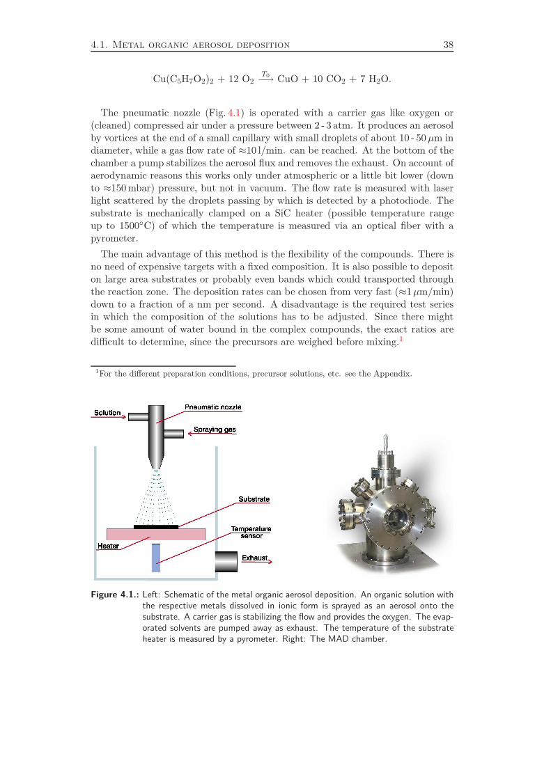
4.1. Metal organic aerosol deposition 38
Cu(C5H7O2)2 + 12 O2T0−→ CuO + 10 CO2 + 7 H2O.
The pneumatic nozzle (Fig. 4.1) is operated with a carrier gas like oxygen or(cleaned) compressed air under a pressure between 2 - 3 atm. It produces an aerosolby vortices at the end of a small capillary with small droplets of about 10 - 50µm indiameter, while a gas flow rate of ≈10 l/min. can be reached. At the bottom of thechamber a pump stabilizes the aerosol flux and removes the exhaust. On account ofaerodynamic reasons this works only under atmospheric or a little bit lower (downto ≈150 mbar) pressure, but not in vacuum. The flow rate is measured with laserlight scattered by the droplets passing by which is detected by a photodiode. Thesubstrate is mechanically clamped on a SiC heater (possible temperature rangeup to 1500C) of which the temperature is measured via an optical fiber with apyrometer.
The main advantage of this method is the flexibility of the compounds. There isno need of expensive targets with a fixed composition. It is also possible to depositon large area substrates or probably even bands which could transported throughthe reaction zone. The deposition rates can be chosen from very fast (≈1µm/min)down to a fraction of a nm per second. A disadvantage is the required test seriesin which the composition of the solutions has to be adjusted. Since there mightbe some amount of water bound in the complex compounds, the exact ratios aredifficult to determine, since the precursors are weighed before mixing.1
1For the different preparation conditions, precursor solutions, etc. see the Appendix.
Figure 4.1.: Left: Schematic of the metal organic aerosol deposition. An organic solution withthe respective metals dissolved in ionic form is sprayed as an aerosol onto thesubstrate. A carrier gas is stabilizing the flow and provides the oxygen. The evap-orated solvents are pumped away as exhaust. The temperature of the substrateheater is measured by a pyrometer. Right: The MAD chamber.
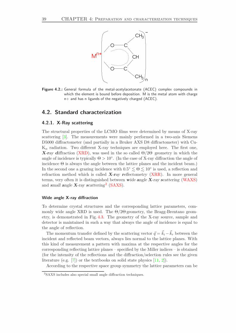
39 CHAPTER 4: Preparation and characterization techniques
−CH
3CH
C
C
O
CH
O
n+
n
M
3
Figure 4.2.: General formula of the metal-acetylacetonate (ACEC) complex compounds inwhich the element is bound before deposition. M is the metal atom with chargen+ and has n ligands of the negatively charged (ACEC).
4.2. Standard characterization
4.2.1. X-Ray scattering
The structural properties of the LCMO films were determined by means of X-rayscattering [3]. The measurements were mainly performed in a two-axis SiemensD5000 diffractometer (and partially in a Bruker AXS D8 diffractometer) with Cu-Kα radiation. Two different X-ray techniques are employed here. The first one,X-ray diffraction (XRD), was used in the so called Θ/2Θ geometry in which theangle of incidence is typically Θ > 10. (In the case of X-ray diffraction the angle ofincidence Θ is always the angle between the lattice planes and the incident beam.)In the second one a grazing incidence with 0.5 . Θ . 10 is used, a reflection andrefraction method which is called X-ray reflectometry (XRR). In more generalterms, very often it is distinguished between wide angle X-ray scattering (WAXS)and small angle X-ray scattering2 (SAXS).
Wide angle X-ray diffraction
To determine crystal structures and the corresponding lattice parameters, com-monly wide angle XRD is used. The Θ/2Θ geometry, the Bragg-Brentano geom-etry, is demonstrated in Fig. 4.3. The geometry of the X-ray source, sample anddetector is maintained in such a way that always the angle of incidence is equal tothe angle of reflection.
The momentum transfer defined by the scattering vector ~q = ~ki−~kr between theincident and reflected beam vectors, always lies normal to the lattice planes. Withthis kind of measurement a pattern with maxima at the respective angles for thecorresponding reflecting lattice planes – specified by the Miller indices – is obtained(for the intensity of the reflections and the diffraction/selection rules see the givenliterature (e.g. [7]) or the textbooks on solid state physics [11, 2]).
According to the respective space group symmetry the lattice parameters can be
2SAXS includes also special small angle diffraction techniques.
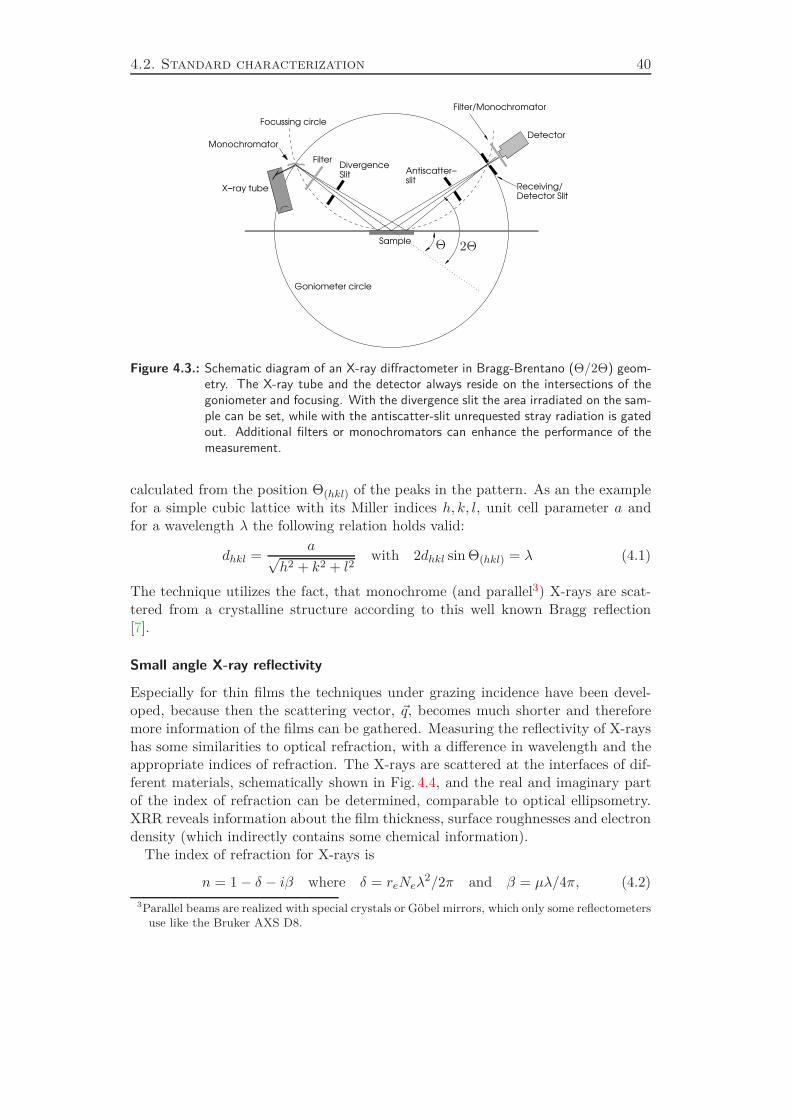
4.2. Standard characterization 40
X−ray tube
DivergenceSlit Antiscatter−
slit
Filter/Monochromator
Receiving/Detector Slit
Focussing circle
MonochromatorDetector
Sample
Goniometer circle
Filter
Θ 2Θ
Figure 4.3.: Schematic diagram of an X-ray diffractometer in Bragg-Brentano (Θ/2Θ) geom-etry. The X-ray tube and the detector always reside on the intersections of thegoniometer and focusing. With the divergence slit the area irradiated on the sam-ple can be set, while with the antiscatter-slit unrequested stray radiation is gatedout. Additional filters or monochromators can enhance the performance of themeasurement.
calculated from the position Θ(hkl) of the peaks in the pattern. As an the examplefor a simple cubic lattice with its Miller indices h, k, l, unit cell parameter a andfor a wavelength λ the following relation holds valid:
dhkl =a√
h2 + k2 + l2with 2dhkl sin Θ(hkl) = λ (4.1)
The technique utilizes the fact, that monochrome (and parallel3) X-rays are scat-tered from a crystalline structure according to this well known Bragg reflection[7].
Small angle X-ray reflectivity
Especially for thin films the techniques under grazing incidence have been devel-oped, because then the scattering vector, ~q, becomes much shorter and thereforemore information of the films can be gathered. Measuring the reflectivity of X-rayshas some similarities to optical refraction, with a difference in wavelength and theappropriate indices of refraction. The X-rays are scattered at the interfaces of dif-ferent materials, schematically shown in Fig. 4.4, and the real and imaginary partof the index of refraction can be determined, comparable to optical ellipsometry.XRR reveals information about the film thickness, surface roughnesses and electrondensity (which indirectly contains some chemical information).
The index of refraction for X-rays is
n = 1− δ − iβ where δ = reNeλ2/2π and β = µλ/4π, (4.2)3Parallel beams are realized with special crystals or Göbel mirrors, which only some reflectometers
use like the Bruker AXS D8.
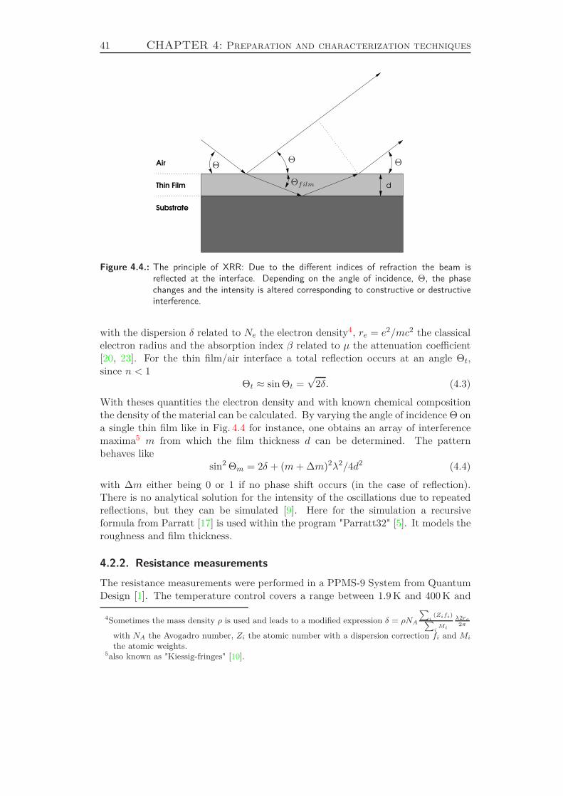
41 CHAPTER 4: Preparation and characterization techniques
Air
Thin Film
Substrate
d
ΘΘ Θ
Θfilm
Figure 4.4.: The principle of XRR: Due to the different indices of refraction the beam isreflected at the interface. Depending on the angle of incidence, Θ, the phasechanges and the intensity is altered corresponding to constructive or destructiveinterference.
with the dispersion δ related to Ne the electron density4, re = e2/mc2 the classicalelectron radius and the absorption index β related to µ the attenuation coefficient[20, 23]. For the thin film/air interface a total reflection occurs at an angle Θt,since n < 1
Θt ≈ sin Θt =√
2δ. (4.3)
With theses quantities the electron density and with known chemical compositionthe density of the material can be calculated. By varying the angle of incidence Θ ona single thin film like in Fig. 4.4 for instance, one obtains an array of interferencemaxima5 m from which the film thickness d can be determined. The patternbehaves like
sin2 Θm = 2δ + (m+ ∆m)2λ2/4d2 (4.4)
with ∆m either being 0 or 1 if no phase shift occurs (in the case of reflection).There is no analytical solution for the intensity of the oscillations due to repeatedreflections, but they can be simulated [9]. Here for the simulation a recursiveformula from Parratt [17] is used within the program "Parratt32" [5]. It models theroughness and film thickness.
4.2.2. Resistance measurements
The resistance measurements were performed in a PPMS-9 System from QuantumDesign [1]. The temperature control covers a range between 1.9 K and 400 K and
4Sometimes the mass density ρ is used and leads to a modified expression δ = ρNA
∑
i(Zifi)∑
iMi
λ2re2π
with NA the Avogadro number, Zi the atomic number with a dispersion correction fi and Mithe atomic weights.
5also known as "Kiessig-fringes" [10].
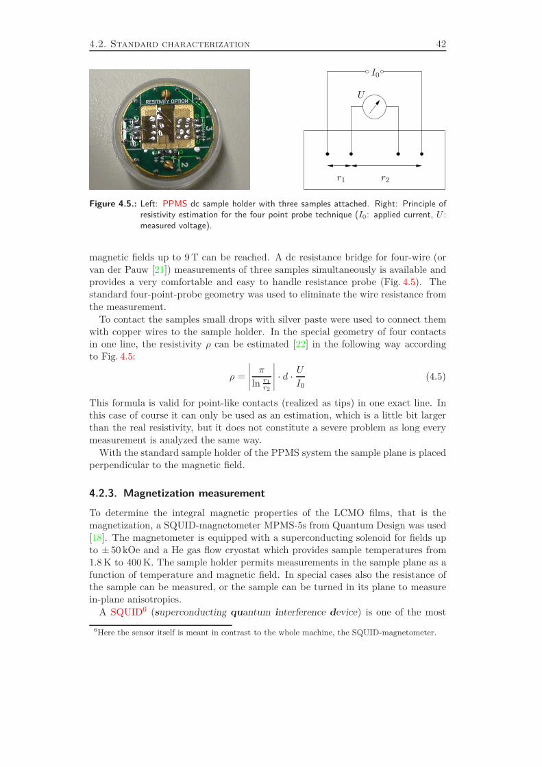
4.2. Standard characterization 42
U
I0
r1 r2
Figure 4.5.: Left: PPMS dc sample holder with three samples attached. Right: Principle ofresistivity estimation for the four point probe technique (I0: applied current, U :measured voltage).
magnetic fields up to 9 T can be reached. A dc resistance bridge for four-wire (orvan der Pauw [21]) measurements of three samples simultaneously is available andprovides a very comfortable and easy to handle resistance probe (Fig. 4.5). Thestandard four-point-probe geometry was used to eliminate the wire resistance fromthe measurement.
To contact the samples small drops with silver paste were used to connect themwith copper wires to the sample holder. In the special geometry of four contactsin one line, the resistivity ρ can be estimated [22] in the following way accordingto Fig. 4.5:
ρ =
∣
∣
∣
∣
∣
π
ln r1r2
∣
∣
∣
∣
∣
· d · UI0
(4.5)
This formula is valid for point-like contacts (realized as tips) in one exact line. Inthis case of course it can only be used as an estimation, which is a little bit largerthan the real resistivity, but it does not constitute a severe problem as long everymeasurement is analyzed the same way.
With the standard sample holder of the PPMS system the sample plane is placedperpendicular to the magnetic field.
4.2.3. Magnetization measurement
To determine the integral magnetic properties of the LCMO films, that is themagnetization, a SQUID-magnetometer MPMS-5s from Quantum Design was used[18]. The magnetometer is equipped with a superconducting solenoid for fields upto ± 50 kOe and a He gas flow cryostat which provides sample temperatures from1.8 K to 400 K. The sample holder permits measurements in the sample plane as afunction of temperature and magnetic field. In special cases also the resistance ofthe sample can be measured, or the sample can be turned in its plane to measurein-plane anisotropies.
A SQUID6 (superconducting quantum interference device) is one of the most
6Here the sensor itself is meant in contrast to the whole machine, the SQUID-magnetometer.
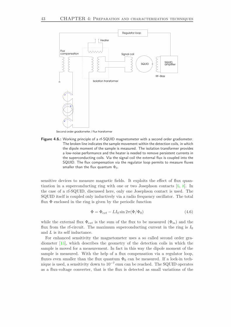
43 CHAPTER 4: Preparation and characterization techniques
Regulator loop
Fluxcompensation
SQUID
Heater
SQUID amplifier
Second order gradiometer / Flux transformer
RF−Bias
Isolation transformer
Signal coil
Figure 4.6.: Working principle of a rf-SQUID magnetometer with a second order gradiometer.The broken line indicates the sample movement within the detection coils, in whichthe dipole moment of the sample is measured. The isolation transformer providesa low-noise performance and the heater is needed to remove persistent currents inthe superconducting coils. Via the signal coil the external flux is coupled into theSQUID. The flux compensation via the regulator loop permits to measure fluxessmaller than the flux quantum Φ0.
sensitive devices to measure magnetic fields. It exploits the effect of flux quan-tization in a superconducting ring with one or two Josephson contacts [6, 8]. Inthe case of a rf-SQUID, discussed here, only one Josephson contact is used. TheSQUID itself is coupled only inductively via a radio frequency oscillator. The totalflux Φ enclosed in the ring is given by the periodic function
Φ = Φext − LI0 sin 2π(Φ/Φ0) (4.6)
while the external flux Φext is the sum of the flux to be measured (Φm) and theflux from the rf-circuit. The maximum superconducting current in the ring is I0and L is its self inductance.
For enhanced sensitivity the magnetometer uses a so called second order gra-diometer [13], which describes the geometry of the detection coils in which thesample is moved for a measurement. In fact in this way the dipole moment of thesample is measured. With the help of a flux compensation via a regulator loop,fluxes even smaller than the flux quantum Φ0 can be measured. If a lock-in tech-nique is used, a sensitivity down to 10−7 emu can be reached. The SQUID operatesas a flux-voltage converter, that is the flux is detected as small variations of the

4.2. Standard characterization 44
voltage in the detection system (see also Fig. 4.6). With the help of a computerbased measurement system, different measurements can be recorded automatically.For a more detailed description of the system see also [4].
45 Bibliography
Bibliography
[1] PPMS – Physical property measurement system. Technical Report Rev. 9.06,Quantum Design, 2006. www.qdusa.com.
[2] N. W. Ashcroft and N. D. Mermin. Solid State Physics. Saunders CollegePublishing, 1976.
[3] M. Birkholz. Thin Film Analysis by X-Ray Scattering. WILEY-VCH VerlagGmbH & Co. KGaA, 2006.
[4] A. Bracchi. Structural and Magnetic Properties of the Glass-Forming Alloy
Nd60Fe30Al10. PhD thesis, University of Göttingen, 2004.
[5] Christian Braun. Parratt32 - or the reflectivity tool. HMI Berlin, 1997-2002.
[6] W. Buckel. Supraleitung - Grundlagen und Anwendungen. Physik Verlag.
[7] B. D. Cullity. Elements of X-ray Diffraction. Addison-Wesley, USA, 1987.
[8] E. du Trémolet de Lacheisserie, D. Gignoux, and M. Schlenker, editors. Mag-
netism, II - Materials and Applications. Kluwer Academic Publishers, 2002.
[9] V. Holý, U. Pietsch, and T. Baumbach. High-resolution X-ray scattering: from
thin films and multilayers. Springer tracts in modern physics. Springer Verlag,1999.
[10] H. Kiessig. Ann. d. Phys., 10:769, 1931.
[11] C. Kittel. Einführung in die Festkörperphysik. Oldenbourg Verlag GmbH,München, 1980.
[12] I. V. Koroshun, E. V. Kryaev, V. T. Moshnyaga, G. A. Klosse, M. A. Krachun,V. M. Zakosarenko, and V. Yu. Davydov. Supercond. Sci. Technol., 3:493,1990.
[13] Mike McElfresh. Fundamentals of magnetism and magnetic measurements:Featuring quantum design’s magnetic property measurement system. Techni-cal report, Purdue University, 1994.
[14] V. Moshnyaga. Metalorganic aerosol deposition technique. Personal commu-nication.
[15] V. Moshnyaga, I. Khoroshun, A. Sidorenko, P. Petrenko, A. Weidinger,M. Zeitler, B. Rauschenbach, R. Tidecks, and K. Samwer. Appl. Phys. Lett.,74:2842, 1999.
[16] V. Moshnyaga, I. V. Koroshun, and E. V. Karyaev. Preparation of oxide thinfilms from coordination compounds. Unpublished.
[17] L. G. Parratt. Phys. Rev., 2:359, 1954.

Bibliography 46
[18] Quantum Design. MPMS XL Hardware Reference Manual, 1996.
[19] D. L. Schulz and T. J. Marks. Advanced Materials, 6:719, 1994.
[20] A. Segemüller. Thin Solid Films, 18:287, 1973.
[21] L. J. van der Pauw. Philips Technical Report, 26:220, 1958.
[22] R. von Helmolt. Magnetowiderstandseffekte in heterogenen Legierungen und
magnetischen Oxiden. Doktorarbeit, Universität Augsburg, 1995.
[23] G. Zorn. The new Siemens X-ray reflectometer. Analytical Application NotesAusg. 1, SIEMENS AG, Jan. 1994.
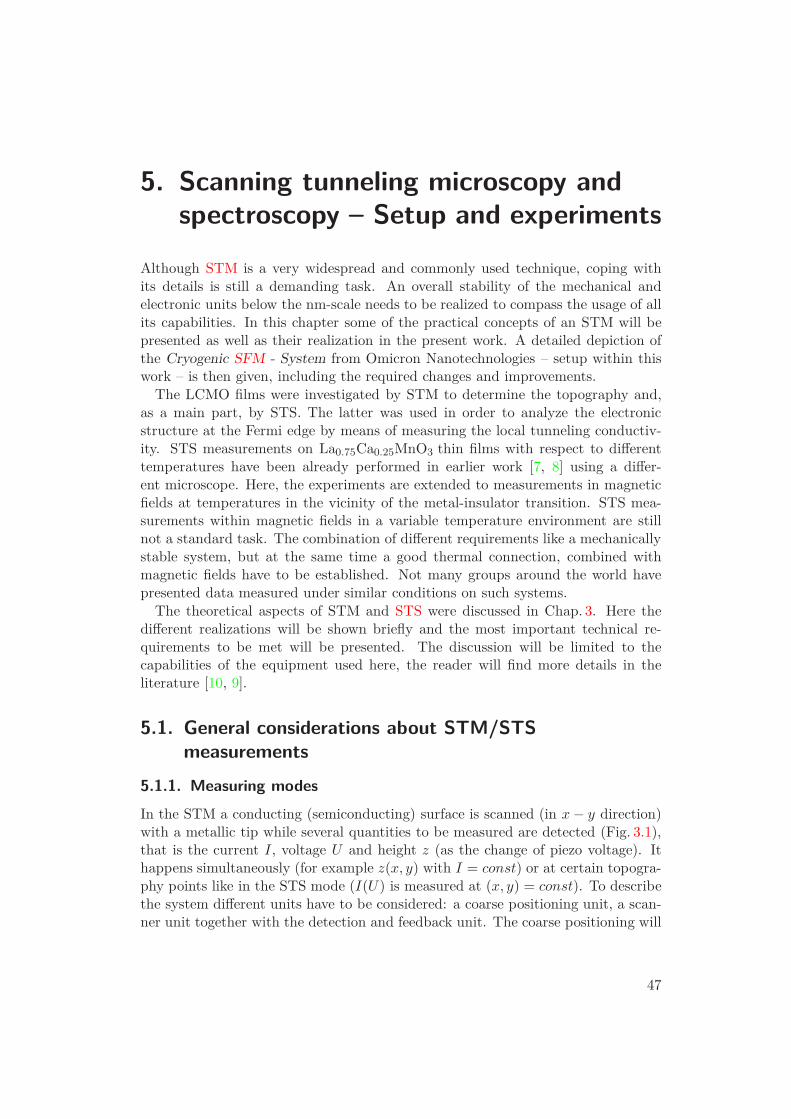
5. Scanning tunneling microscopy andspectroscopy – Setup and experiments
Although STM is a very widespread and commonly used technique, coping withits details is still a demanding task. An overall stability of the mechanical andelectronic units below the nm-scale needs to be realized to compass the usage of allits capabilities. In this chapter some of the practical concepts of an STM will bepresented as well as their realization in the present work. A detailed depiction ofthe Cryogenic SFM - System from Omicron Nanotechnologies – setup within thiswork – is then given, including the required changes and improvements.
The LCMO films were investigated by STM to determine the topography and,as a main part, by STS. The latter was used in order to analyze the electronicstructure at the Fermi edge by means of measuring the local tunneling conductiv-ity. STS measurements on La0.75Ca0.25MnO3 thin films with respect to differenttemperatures have been already performed in earlier work [7, 8] using a differ-ent microscope. Here, the experiments are extended to measurements in magneticfields at temperatures in the vicinity of the metal-insulator transition. STS mea-surements within magnetic fields in a variable temperature environment are stillnot a standard task. The combination of different requirements like a mechanicallystable system, but at the same time a good thermal connection, combined withmagnetic fields have to be established. Not many groups around the world havepresented data measured under similar conditions on such systems.
The theoretical aspects of STM and STS were discussed in Chap. 3. Here thedifferent realizations will be shown briefly and the most important technical re-quirements to be met will be presented. The discussion will be limited to thecapabilities of the equipment used here, the reader will find more details in theliterature [10, 9].
5.1. General considerations about STM/STSmeasurements
5.1.1. Measuring modes
In the STM a conducting (semiconducting) surface is scanned (in x− y direction)with a metallic tip while several quantities to be measured are detected (Fig. 3.1),that is the current I, voltage U and height z (as the change of piezo voltage). Ithappens simultaneously (for example z(x, y) with I = const) or at certain topogra-phy points like in the STS mode (I(U) is measured at (x, y) = const). To describethe system different units have to be considered: a coarse positioning unit, a scan-ner unit together with the detection and feedback unit. The coarse positioning will
47
5.1. General considerations about STM/STS measurements 48
Scan size
I(U)
Speed
Sample
Hi−Voltage Amplifierz
y
x
I
Feedback Loop
Loop Gain
external noise
low pass 100kHz
DAC
Co
mp
ute
rin
terf
ac
e /
Dig
ita
l Co
ntr
ol
Tip
U
Set Point
Spec.
USet Point
Topography
Comparator
Error Signal
I
U
Log. Amplifier
IVC
ADC
Tunnel
DAC
junction
ScanningUnit
Pre−AmplifierBox
FeedbackControl
x,y,zScan−piezo
ReferenceControl &Logic
I 0
I 0
Figure 5.1.: Schematic diagram of the feedback system for the constant current mode. Thefeedback loop is marked in red: The tunneling current I is measured, amplifiedand then compared as a converted voltage with the reference signal given bythe user via a computer digital control system. The error signal, that is thedifference to the reference, converted into a respective voltage is used to drivethe z-piezo, which is adjusted to regain the reference value of the current. Atthe same time the error signal corresponds to the changes in topography (or moreprecisely constant electron density) and is recorded by the computer as the z-signalreproducing the topographic features. Also the voltage U is set via the controlunit and it transverses a low pass filter. In case of the spectroscopy measurementsthe comparator and feedback control are switched off. The parts responsive toexternal noise are marked with blue arrows. (IVC: current/voltage converter, VIC:
voltage/current converter, ADC: analog/digital converter, DAC: digital/analog converter)
be described together with the microscope itself (Sec. 5.2).The sample movement is accomplished by a piezo drive while piezoelectric coeffi-
cients down to 0.2 nm/V can be easily established 1. One of the important fields isthe electronics responsible for the feedback loop and especially the sample and holdcircuits, which are used, if the STS measurements are implemented in a topographymeasurement.
The most commonly used measuring mode of an STM is the constant current
mode, in which the current is kept constant (I = const) and the topography ismeasured as the height changes of the piezo, z(x, y). It provides the possibility tolook at not well known surfaces without too much danger to damage the tip (orsurface). The constant height mode (z = const) which measures I(x, y) for examplerequires some prerequisites like a quite smooth surface and therefore small scanningareas to prevent the tip running into any obstacles, but might be advantageous foratomic resolution pictures.
In this case only the constant current mode was used and its working principle isdrawn in Fig. 5.1. A fixed bias is applied to the sample and the tip is approacheduntil a pre-defined tunneling current is achieved (the tip-sample distance is herebytypically ≈ 0.1 nm). To maintain the current during scanning it is constantly
1It is easy to find construction guidances for very simple (home-built) STMs in air.
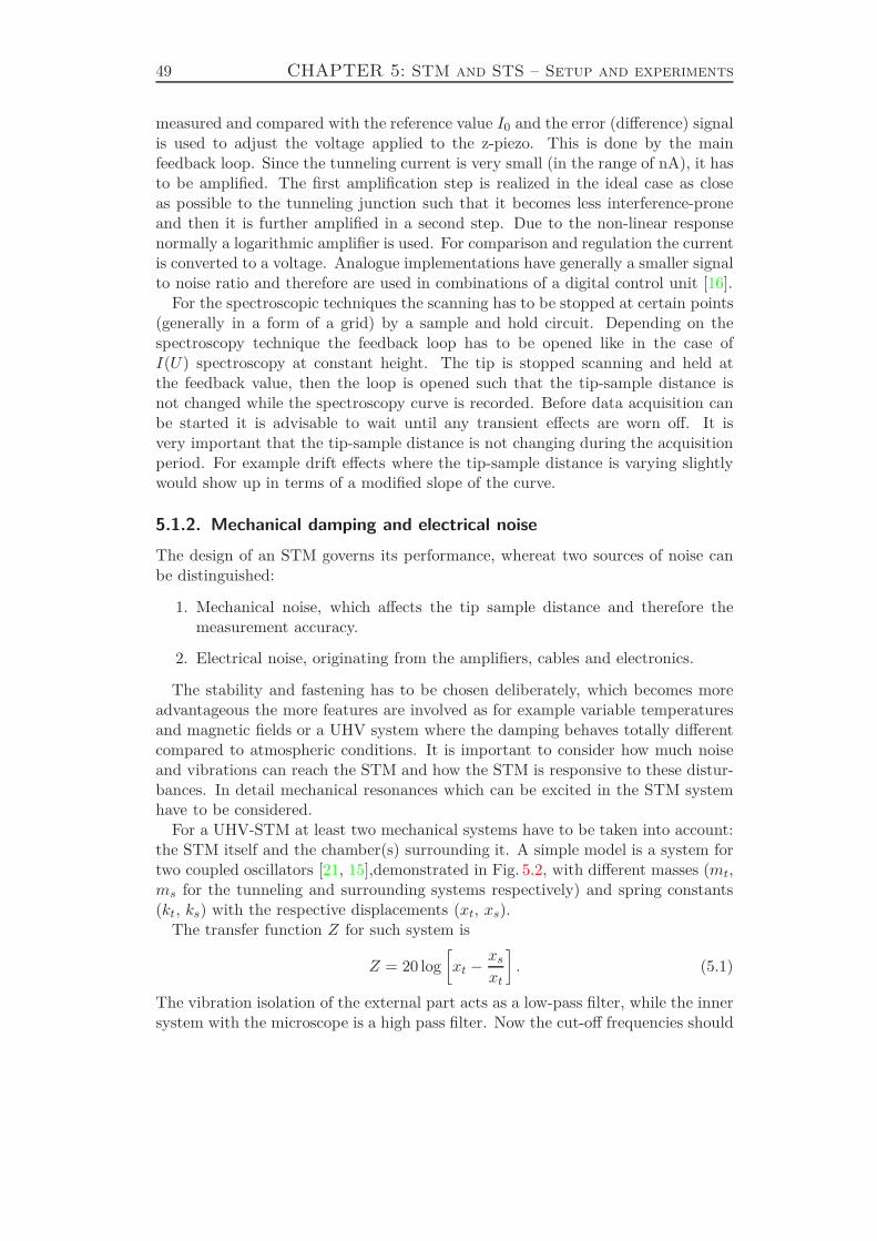
49 CHAPTER 5: STM and STS – Setup and experiments
measured and compared with the reference value I0 and the error (difference) signalis used to adjust the voltage applied to the z-piezo. This is done by the mainfeedback loop. Since the tunneling current is very small (in the range of nA), it hasto be amplified. The first amplification step is realized in the ideal case as closeas possible to the tunneling junction such that it becomes less interference-proneand then it is further amplified in a second step. Due to the non-linear responsenormally a logarithmic amplifier is used. For comparison and regulation the currentis converted to a voltage. Analogue implementations have generally a smaller signalto noise ratio and therefore are used in combinations of a digital control unit [16].
For the spectroscopic techniques the scanning has to be stopped at certain points(generally in a form of a grid) by a sample and hold circuit. Depending on thespectroscopy technique the feedback loop has to be opened like in the case ofI(U) spectroscopy at constant height. The tip is stopped scanning and held atthe feedback value, then the loop is opened such that the tip-sample distance isnot changed while the spectroscopy curve is recorded. Before data acquisition canbe started it is advisable to wait until any transient effects are worn off. It isvery important that the tip-sample distance is not changing during the acquisitionperiod. For example drift effects where the tip-sample distance is varying slightlywould show up in terms of a modified slope of the curve.
5.1.2. Mechanical damping and electrical noise
The design of an STM governs its performance, whereat two sources of noise canbe distinguished:
1. Mechanical noise, which affects the tip sample distance and therefore themeasurement accuracy.
2. Electrical noise, originating from the amplifiers, cables and electronics.
The stability and fastening has to be chosen deliberately, which becomes moreadvantageous the more features are involved as for example variable temperaturesand magnetic fields or a UHV system where the damping behaves totally differentcompared to atmospheric conditions. It is important to consider how much noiseand vibrations can reach the STM and how the STM is responsive to these distur-bances. In detail mechanical resonances which can be excited in the STM systemhave to be considered.
For a UHV-STM at least two mechanical systems have to be taken into account:the STM itself and the chamber(s) surrounding it. A simple model is a system fortwo coupled oscillators [21, 15],demonstrated in Fig. 5.2, with different masses (mt,ms for the tunneling and surrounding systems respectively) and spring constants(kt, ks) with the respective displacements (xt, xs).
The transfer function Z for such system is
Z = 20 log[
xt −xsxt
]
. (5.1)
The vibration isolation of the external part acts as a low-pass filter, while the innersystem with the microscope is a high pass filter. Now the cut-off frequencies should
5.2. The Cryogenic SFM by Omicron 50
STM/Surrounding
STM/Ground
ms
mt
ks
kt
xs
x t
Ground
Chamber/Surrounding
STM
Tra
nsf
er
fun
ctio
n
Frequency
1
Surrounding/Ground
Coupled system
Figure 5.2.: Left: Vibrational system as a coupled oscillator of the STM and the surround-ing chamber. Right: Schematic drawing of the transfer functions for the noisepropagation.
be as far away as possible and the plateau in between (see Fig. 5.2) should be aslow as possible.
Another contribution to noise in the tunnel current measurement comes from thecoaxial cable used for the connection between tip and pre-amplifier. Coaxial cablesrepresent capacitors which are not absolutely stiff on very small scales. Their partscan move against each other due to sound noise resulting in a change of capacitanceC with time t. This induces small voltage changes dU and leads to small currents
I = CdU
dt+ UdC
dt(5.2)
These small disturbances are amplified together with the tunneling current andare one major source of noise. In general there are suitable amplifiers availablewhich can be mounted directly into the UHV, but with the additional temperaturechanges it is nearly impossible to establish a stable working amplifier nearby theSTM directly in the chamber. Therefore a low pass filter in the feedback system isindispensable.
5.2. The Cryogenic SFM by Omicron
The Cryogenic SFM (scanning force microscope) in Fig. 5.9 from Omicron is a sys-tem with a combined STM and AFM/MFM (atomic/magnetic force microscope)measuring head. The microscope is placed in a UHV chamber within a cryostatfrom Oxford Instruments. Sample temperatures in between 7 K and RT (300 K)and magnetic fields up to 8 T can be reached.
The system had to be set up for usage in this work. In microscopes of this typethe connection of thermal stability with an undisturbed measuring system is, ingeneral, a demanding task. In the following the system will be described in moredetail split into the different parts. A lot of improvements were required withrespect to the STM usage2 and are described as well in the last part.
2The atomic force microscope was also assembled within this work, but not used for the mainmeasurements; some MFM measurements are presented in the appendix.
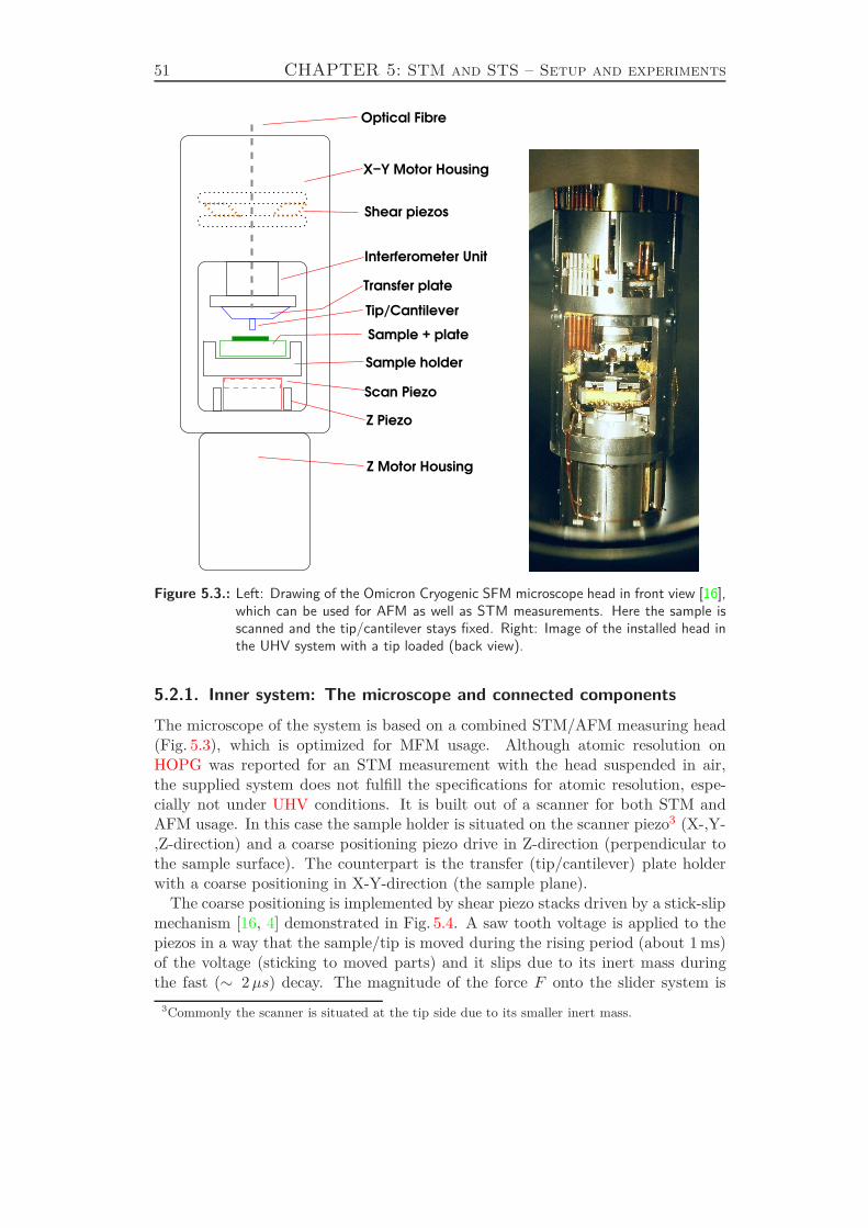
51 CHAPTER 5: STM and STS – Setup and experiments
Optical Fibre
Sample + plate
Tip/Cantilever
Transfer plate
Interferometer Unit
Shear piezos
X−Y Motor Housing
Z Motor Housing
Z Piezo
Scan Piezo
Sample holder
Figure 5.3.: Left: Drawing of the Omicron Cryogenic SFM microscope head in front view [16],which can be used for AFM as well as STM measurements. Here the sample isscanned and the tip/cantilever stays fixed. Right: Image of the installed head inthe UHV system with a tip loaded (back view).
5.2.1. Inner system: The microscope and connected components
The microscope of the system is based on a combined STM/AFM measuring head(Fig. 5.3), which is optimized for MFM usage. Although atomic resolution onHOPG was reported for an STM measurement with the head suspended in air,the supplied system does not fulfill the specifications for atomic resolution, espe-cially not under UHV conditions. It is built out of a scanner for both STM andAFM usage. In this case the sample holder is situated on the scanner piezo3 (X-,Y-,Z-direction) and a coarse positioning piezo drive in Z-direction (perpendicular tothe sample surface). The counterpart is the transfer (tip/cantilever) plate holderwith a coarse positioning in X-Y-direction (the sample plane).
The coarse positioning is implemented by shear piezo stacks driven by a stick-slipmechanism [16, 4] demonstrated in Fig. 5.4. A saw tooth voltage is applied to thepiezos in a way that the sample/tip is moved during the rising period (about 1 ms)of the voltage (sticking to moved parts) and it slips due to its inert mass duringthe fast (∼ 2µs) decay. The magnitude of the force F onto the slider system is
3Commonly the scanner is situated at the tip side due to its smaller inert mass.
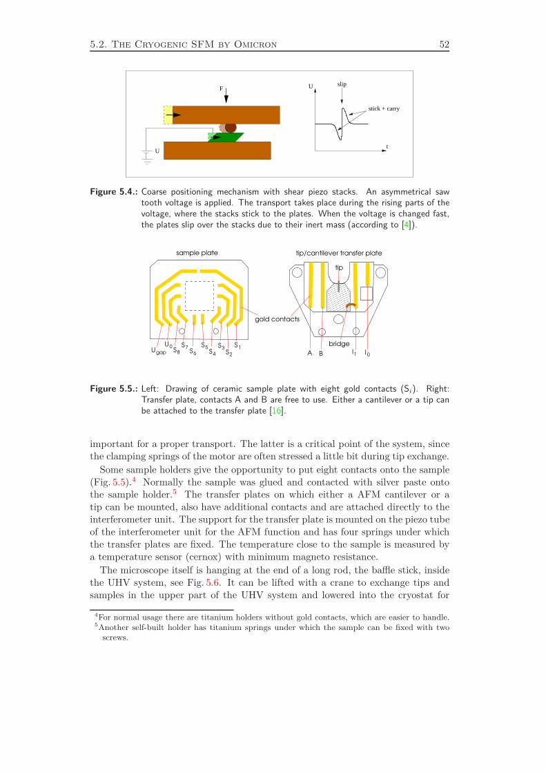
5.2. The Cryogenic SFM by Omicron 52
U
stick + carry
U
t
slipF
Figure 5.4.: Coarse positioning mechanism with shear piezo stacks. An asymmetrical sawtooth voltage is applied. The transport takes place during the rising parts of thevoltage, where the stacks stick to the plates. When the voltage is changed fast,the plates slip over the stacks due to their inert mass (according to [4]).
3 S1S5S7U0
Ugap S8 S6 S4 S2 TI I0
bridge
sample plate
A B
tip/cantilever transfer plate
tip
gold contacts
S
Figure 5.5.: Left: Drawing of ceramic sample plate with eight gold contacts (Si). Right:Transfer plate, contacts A and B are free to use. Either a cantilever or a tip canbe attached to the transfer plate [16].
important for a proper transport. The latter is a critical point of the system, sincethe clamping springs of the motor are often stressed a little bit during tip exchange.
Some sample holders give the opportunity to put eight contacts onto the sample(Fig. 5.5).4 Normally the sample was glued and contacted with silver paste ontothe sample holder.5 The transfer plates on which either a AFM cantilever or atip can be mounted, also have additional contacts and are attached directly to theinterferometer unit. The support for the transfer plate is mounted on the piezo tubeof the interferometer unit for the AFM function and has four springs under whichthe transfer plates are fixed. The temperature close to the sample is measured bya temperature sensor (cernox) with minimum magneto resistance.
The microscope itself is hanging at the end of a long rod, the baffle stick, insidethe UHV system, see Fig. 5.6. It can be lifted with a crane to exchange tips andsamples in the upper part of the UHV system and lowered into the cryostat for
4For normal usage there are titanium holders without gold contacts, which are easier to handle.5Another self-built holder has titanium springs under which the sample can be fixed with two
screws.
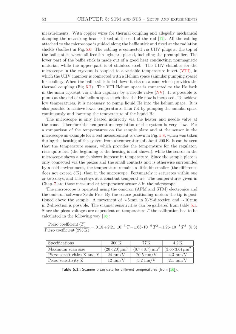
53 CHAPTER 5: STM and STS – Setup and experiments
measurements. With copper wires for thermal coupling and allegedly mechanicaldamping the measuring head is fixed at the end of the rod [12]. All the cablingattached to the microscope is guided along the baffle stick and fixed at the radiationshields (baffles) in Fig. 5.6. The cabling is connected via UHV plugs at the top ofthe baffle stick where all feedthroughs are placed, including the preamplifier. Thelower part of the baffle stick is made out of a good heat conducting, nonmagneticmaterial, while the upper part is of stainless steel. The UHV chamber for themicroscope in the cryostat is coupled to a variable temperature insert (VTI), inwhich the UHV chamber is connected with a Helium space (annular pumping space)for cooling. When the baffle stick is led down it sits on a cone which provides thethermal coupling (Fig. 5.7). The VTI Helium space is connected to the He bathin the main cryostat via a thin capillary by a needle valve (NV). It is possible topump at the end of the helium space such that the He flow is increased. To achievelow temperatures, it is necessary to pump liquid He into the helium space. It isalso possible to achieve lower temperatures than 7 K by pumping the annular spacecontinuously and lowering the temperature of the liquid He.
The microscope is only heated indirectly via the heater and needle valve atthe cone. Therefore the temperature regulation of the system is very slow. Fora comparison of the temperatures on the sample plate and at the sensor in themicroscope an example for a test measurement is shown in Fig. 5.8, which was takenduring the heating of the system from a temperature of about 200 K. It can be seenthat the temperature sensor, which provides the temperature for the regulator,rises quite fast (the beginning of the heating is not shown), while the sensor in themicroscope shows a much slower increase in temperature. Since the sample plate isonly connected via the piezos and the small contacts and is otherwise surroundedby a cold environment, the temperature remains a little bit smaller (the differencedoes not exceed 5 K), than in the microscope. Fortunately it saturates within oneor two days, and then stays at a constant temperature. The temperatures given inChap. 7 are those measured at temperature sensor 3 in the microscope.
The microscope is operated using the omicron (AFM and STM) electronics andthe omicron software Scala Pro. By the coarse positioning motors the tip is posi-tioned above the sample. A movement of ∼ 5 mm in X-Y-direction and ∼ 10 mmin Z-direction is possible. The scanner sensitivities can be gathered from table 5.1.Since the piezo voltages are dependent on temperature T the calibration has to becalculated in the following way [16]:
Piezo coefficient (T )Piezo coefficient (293 K)
= 0.18+2.21·10−3 T−1.63·10−6 T 2 +1.26·10−8 T 3 (5.3)
Specifications 300 K 77 K 4.2 K
Maximum scan size (20×20) µm2 (8.7×8.7) µm2 (3.6×3.6) µm2
Piezo sensitivities X and Y 24 nm/V 20.5 nm/V 4.3 nm/VPiezo sensitivity Z 12 nm/V 5.2 nm/V 2.1 nm/V
Table 5.1.: Scanner piezo data for different temperatures (from [16]).
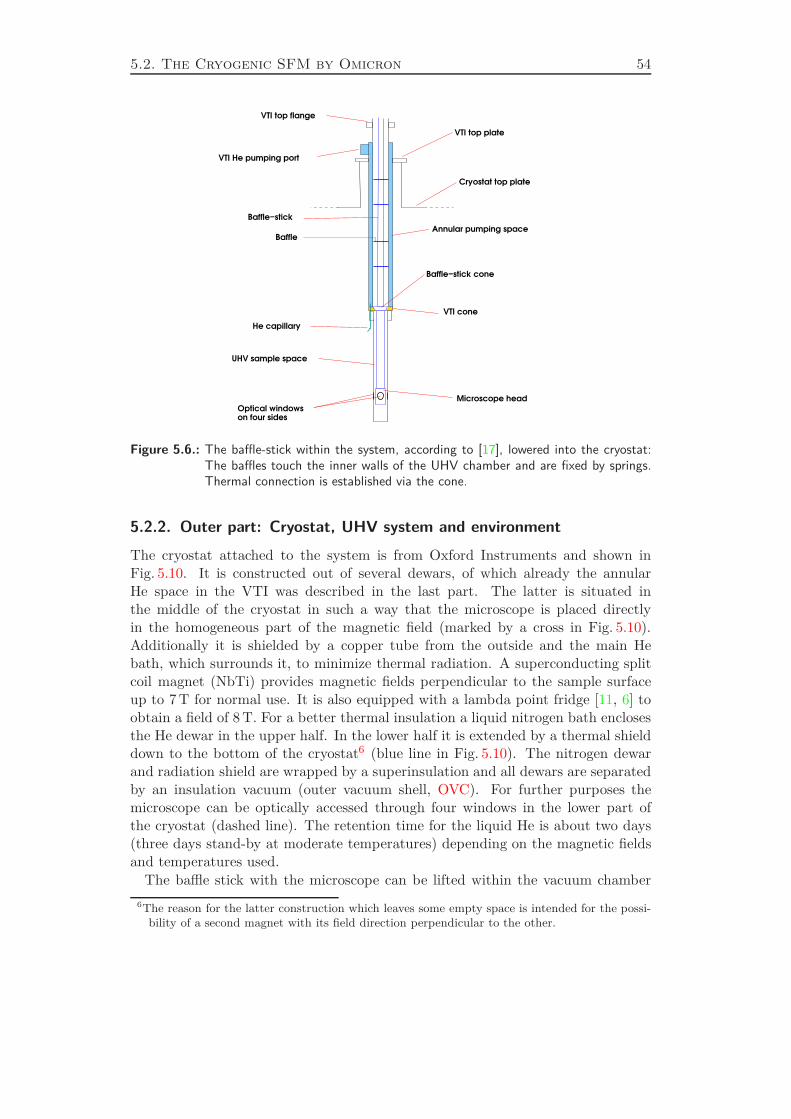
5.2. The Cryogenic SFM by Omicron 54
on four sides
Baffle−stick cone
Microscope head
Baffle−stick
VTI He pumping port
VTI top flange
Baffle
He capillary
UHV sample space
Optical windows
VTI cone
VTI top plate
Cryostat top plate
Annular pumping space
Figure 5.6.: The baffle-stick within the system, according to [17], lowered into the cryostat:The baffles touch the inner walls of the UHV chamber and are fixed by springs.Thermal connection is established via the cone.
5.2.2. Outer part: Cryostat, UHV system and environment
The cryostat attached to the system is from Oxford Instruments and shown inFig. 5.10. It is constructed out of several dewars, of which already the annularHe space in the VTI was described in the last part. The latter is situated inthe middle of the cryostat in such a way that the microscope is placed directlyin the homogeneous part of the magnetic field (marked by a cross in Fig. 5.10).Additionally it is shielded by a copper tube from the outside and the main Hebath, which surrounds it, to minimize thermal radiation. A superconducting splitcoil magnet (NbTi) provides magnetic fields perpendicular to the sample surfaceup to 7 T for normal use. It is also equipped with a lambda point fridge [11, 6] toobtain a field of 8 T. For a better thermal insulation a liquid nitrogen bath enclosesthe He dewar in the upper half. In the lower half it is extended by a thermal shielddown to the bottom of the cryostat6 (blue line in Fig. 5.10). The nitrogen dewarand radiation shield are wrapped by a superinsulation and all dewars are separatedby an insulation vacuum (outer vacuum shell, OVC). For further purposes themicroscope can be optically accessed through four windows in the lower part ofthe cryostat (dashed line). The retention time for the liquid He is about two days(three days stand-by at moderate temperatures) depending on the magnetic fieldsand temperatures used.
The baffle stick with the microscope can be lifted within the vacuum chamber
6The reason for the latter construction which leaves some empty space is intended for the possi-bility of a second magnet with its field direction perpendicular to the other.
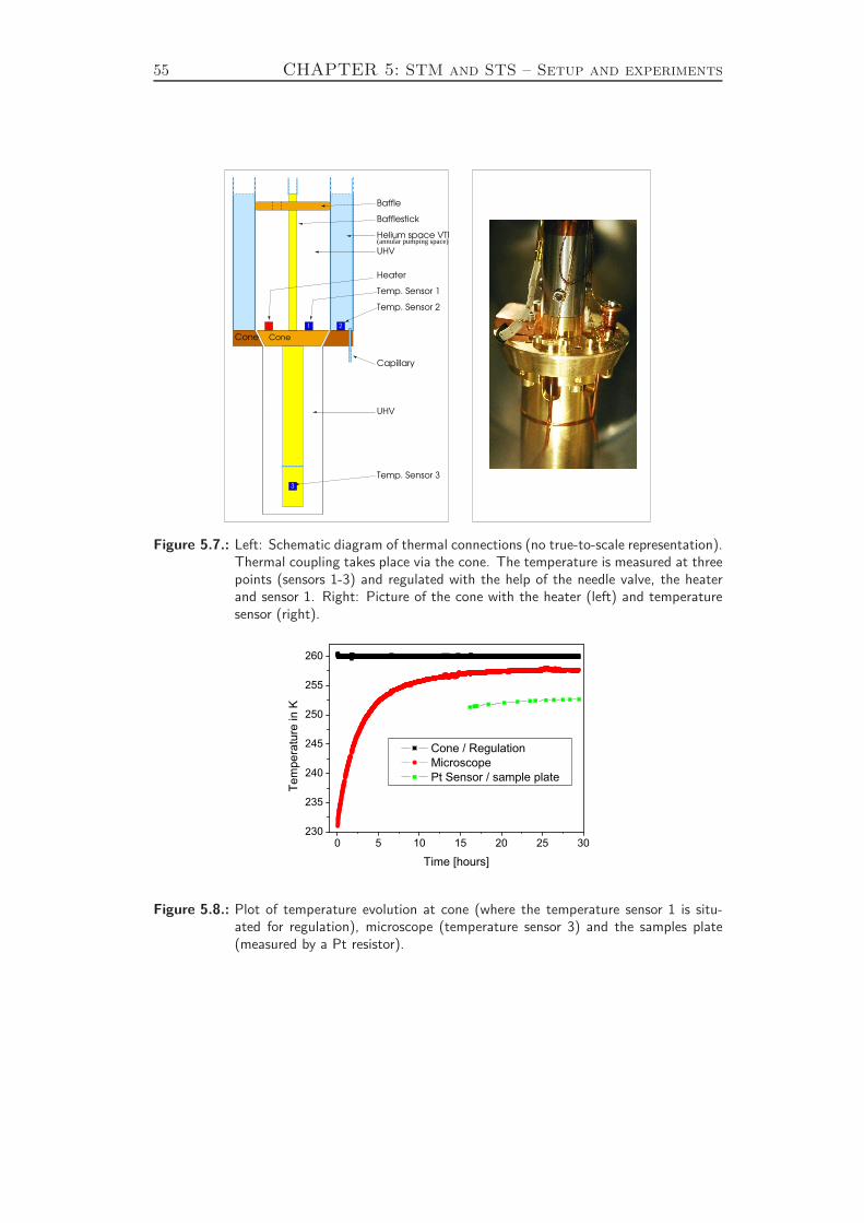
55 CHAPTER 5: STM and STS – Setup and experiments
(annular pumping space)
Cone
Temp. Sensor 1
Temp. Sensor 2
Bafflestick
2
UHV
3
1
Heater
Temp. Sensor 3
Helium space VTI
Capillary
Cone
Baffle
UHV
Figure 5.7.: Left: Schematic diagram of thermal connections (no true-to-scale representation).Thermal coupling takes place via the cone. The temperature is measured at threepoints (sensors 1-3) and regulated with the help of the needle valve, the heaterand sensor 1. Right: Picture of the cone with the heater (left) and temperaturesensor (right).
0 5 10 15 20 25 30230
235
240
245
250
255
260
Tem
pera
ture
in K
Time [hours]
Cone / Regulation Microscope Pt Sensor / sample plate
Figure 5.8.: Plot of temperature evolution at cone (where the temperature sensor 1 is situ-ated for regulation), microscope (temperature sensor 3) and the samples plate(measured by a Pt resistor).
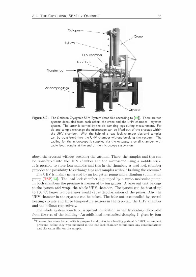
5.2. The Cryogenic SFM by Omicron 56
Load lock
Cryostat
Crane
Bellows
Octopus
UHV chamber
Transfer rod
Air damping legs
Figure 5.9.: The Omicron Cryogenic SFM System (modified according to [16]). There are twosystems decoupled from each other: the crane and the UHV chamber - cryostatsystem. The latter is carried by the air damping legs during measurement. Fortip and sample exchange the microscope can be lifted out of the cryostat withinthe UHV chamber. With the help of a load lock chamber tips and samplescan be transferred into the UHV chamber without breaking the vacuum. Thecabling for the microscope is supplied via the octopus, a small chamber withcable feedthroughs at the end of the microscope suspension.
above the cryostat without breaking the vacuum. There, the samples and tips canbe transferred into the UHV chamber and the microscope using a wobble stick.It is possible to store four samples and tips in the chamber. A load lock chamberprovides the possibility to exchange tips and samples without braking the vacuum.7
The UHV is mainly generated by an ion getter pump and a titanium sublimationpump (TSP)[23]. The load lock chamber is pumped by a turbo molecular pump.In both chambers the pressure is measured by ion gauges. A bake out tent belongsto the system and wraps the whole UHV chamber. The system can be heated upto 150 C, larger temperatures would cause depolarization of the piezos. Also theUHV chamber in the cryostat can be baked. The bake out is controlled by severalheating circuits and three temperature sensors in the cryostat, the UHV chamberand the bellows respectively.
The whole system stands on a special foundation in the laboratory decoupledfrom the rest of the building. An additional mechanical damping is given by four
7The samples were cleaned with isopropanol and put onto a heating plate at > 120C at ambientpressure, before they were mounted in the load lock chamber to minimize any contaminationsand the water film on the sample.
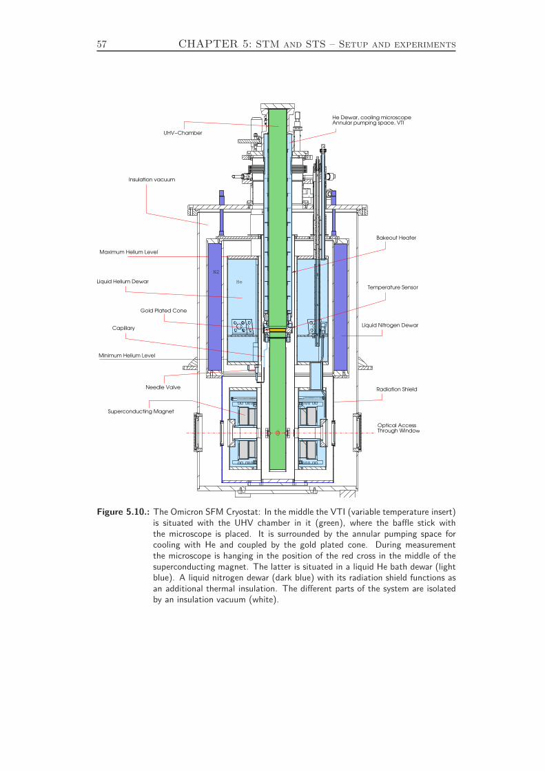
57 CHAPTER 5: STM and STS – Setup and experiments
He
N2
Annular pumping space, VTIHe Dewar, cooling microscope
Superconducting Magnet
Optical AccessThrough Windows
UHV−Chamber
Maximum Helium Level
Insulation vacuum
Minimum Helium Level
Radiation Shield
Liquid Helium Dewar
Liquid Nitrogen DewarCapillary
Gold Plated Cone
Bakeout Heater
Temperature Sensor
Needle Valve
Figure 5.10.: The Omicron SFM Cryostat: In the middle the VTI (variable temperature insert)is situated with the UHV chamber in it (green), where the baffle stick withthe microscope is placed. It is surrounded by the annular pumping space forcooling with He and coupled by the gold plated cone. During measurementthe microscope is hanging in the position of the red cross in the middle of thesuperconducting magnet. The latter is situated in a liquid He bath dewar (lightblue). A liquid nitrogen dewar (dark blue) with its radiation shield functions asan additional thermal insulation. The different parts of the system are isolatedby an insulation vacuum (white).
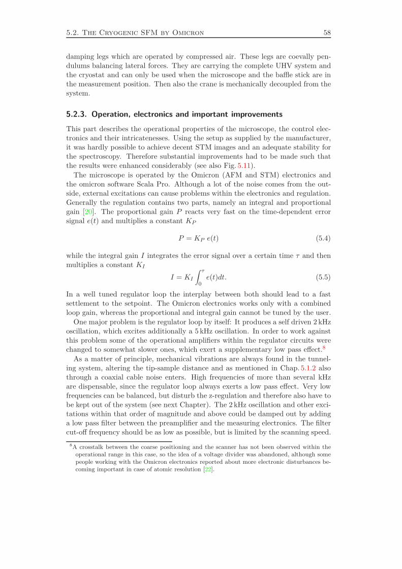
5.2. The Cryogenic SFM by Omicron 58
damping legs which are operated by compressed air. These legs are coevally pen-dulums balancing lateral forces. They are carrying the complete UHV system andthe cryostat and can only be used when the microscope and the baffle stick are inthe measurement position. Then also the crane is mechanically decoupled from thesystem.
5.2.3. Operation, electronics and important improvements
This part describes the operational properties of the microscope, the control elec-tronics and their intricatenesses. Using the setup as supplied by the manufacturer,it was hardly possible to achieve decent STM images and an adequate stability forthe spectroscopy. Therefore substantial improvements had to be made such thatthe results were enhanced considerably (see also Fig. 5.11).
The microscope is operated by the Omicron (AFM and STM) electronics andthe omicron software Scala Pro. Although a lot of the noise comes from the out-side, external excitations can cause problems within the electronics and regulation.Generally the regulation contains two parts, namely an integral and proportionalgain [20]. The proportional gain P reacts very fast on the time-dependent errorsignal e(t) and multiplies a constant KP
P = KP e(t) (5.4)
while the integral gain I integrates the error signal over a certain time τ and thenmultiplies a constant KI
I = KI∫ τ
0e(t)dt. (5.5)
In a well tuned regulator loop the interplay between both should lead to a fastsettlement to the setpoint. The Omicron electronics works only with a combinedloop gain, whereas the proportional and integral gain cannot be tuned by the user.
One major problem is the regulator loop by itself: It produces a self driven 2 kHzoscillation, which excites additionally a 5 kHz oscillation. In order to work againstthis problem some of the operational amplifiers within the regulator circuits werechanged to somewhat slower ones, which exert a supplementary low pass effect.8
As a matter of principle, mechanical vibrations are always found in the tunnel-ing system, altering the tip-sample distance and as mentioned in Chap. 5.1.2 alsothrough a coaxial cable noise enters. High frequencies of more than several kHzare dispensable, since the regulator loop always exerts a low pass effect. Very lowfrequencies can be balanced, but disturb the z-regulation and therefore also have tobe kept out of the system (see next Chapter). The 2 kHz oscillation and other exci-tations within that order of magnitude and above could be damped out by addinga low pass filter between the preamplifier and the measuring electronics. The filtercut-off frequency should be as low as possible, but is limited by the scanning speed.
8A crosstalk between the coarse positioning and the scanner has not been observed within theoperational range in this case, so the idea of a voltage divider was abandoned, although somepeople working with the Omicron electronics reported about more electronic disturbances be-coming important in case of atomic resolution [22].
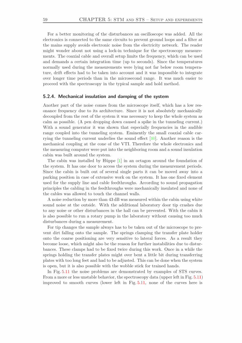
59 CHAPTER 5: STM and STS – Setup and experiments
For a better monitoring of the disturbances an oscilloscope was added. All theelectronics is connected to the same circuits to prevent ground loops and a filter atthe mains supply avoids electronic noise from the electricity network. The readermight wonder about not using a lock-in technique for the spectroscopy measure-ments. The coaxial cable and overall setup limits the frequency, which can be usedand demands a certain integration time (up to seconds). Since the temperaturesnormally used during the measurements were lying not far below room tempera-ture, drift effects had to be taken into account and it was impossible to integrateover longer time periods than in the microsecond range. It was much easier toproceed with the spectroscopy in the typical sample and hold method.
5.2.4. Mechanical insulation and damping of the system
Another part of the noise comes from the microscope itself, which has a low res-onance frequency due to its architecture. Since it is not absolutely mechanicallydecoupled from the rest of the system it was necessary to keep the whole system ascalm as possible. (A pen dropping down caused a spike in the tunneling current.)With a sound generator it was shown that especially frequencies in the audiblerange coupled into the tunneling system. Eminently the small coaxial cable car-rying the tunneling current underlies the sound effect [10]. Another reason is themechanical coupling at the cone of the VTI. Therefore the whole electronics andthe measuring computer were put into the neighboring room and a sound insulationcabin was built around the system.
The cabin was installed by Hüppe [1] in an octagon around the foundation ofthe system. It has one door to access the system during the measurement periods.Since the cabin is built out of several single parts it can be moved away into aparking position in case of extensive work on the system. It has one fixed elementused for the supply line and cable feedthroughs. According to sound propagationprinciples the cabling in the feedthroughs were mechanically insulated and none ofthe cables was allowed to touch the channel walls.
A noise reduction by more than 43 dB was measured within the cabin using whitesound noise at the outside. With the additional laboratory door tip crashes dueto any noise or other disturbances in the hall can be prevented. With the cabin itis also possible to run a rotary pump in the laboratory without causing too muchdisturbances during a measurement.
For tip changes the sample always has to be taken out of the microscope to pre-vent dirt falling onto the sample. The springs clamping the transfer plate holderonto the coarse positioning are very sensitive to lateral forces. As a result theybecome loose, which might also be the reason for further instabilities due to distur-bances. These clamps had to be fixed twice during this work. Once in a while thesprings holding the transfer plates might over bent a little bit during transferringplates with too long feet and had to be adjusted. This can be done when the systemis open, but it is also possible with the wobble stick for trained hands.
In Fig. 5.11 the noise problems are demonstrated by examples of STS curves.From a more or less unstable behavior, the spectroscopy data (upper left in Fig. 5.11)improved to smooth curves (lower left in Fig. 5.11, none of the curves here is
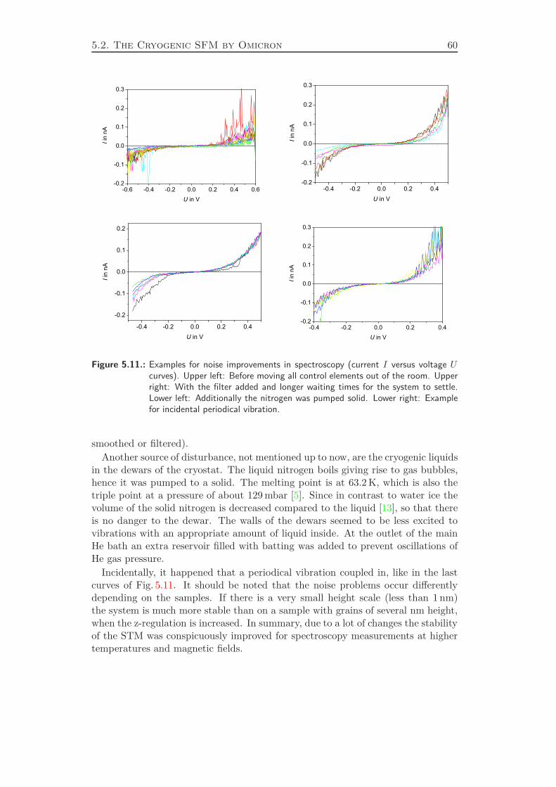
5.2. The Cryogenic SFM by Omicron 60
-0.6 -0.4 -0.2 0.0 0.2 0.4 0.6-0.2
-0.1
0.0
0.1
0.2
0.3
I in
nA
U in V
-0.4 -0.2 0.0 0.2 0.4-0.2
-0.1
0.0
0.1
0.2
0.3
I in
nA
U in V
-0.4 -0.2 0.0 0.2 0.4
-0.2
-0.1
0.0
0.1
0.2
I in
nA
U in V-0.4 -0.2 0.0 0.2 0.4
-0.2
-0.1
0.0
0.1
0.2
0.3
I in
nA
U in V
Figure 5.11.: Examples for noise improvements in spectroscopy (current I versus voltage Ucurves). Upper left: Before moving all control elements out of the room. Upperright: With the filter added and longer waiting times for the system to settle.Lower left: Additionally the nitrogen was pumped solid. Lower right: Examplefor incidental periodical vibration.
smoothed or filtered).Another source of disturbance, not mentioned up to now, are the cryogenic liquids
in the dewars of the cryostat. The liquid nitrogen boils giving rise to gas bubbles,hence it was pumped to a solid. The melting point is at 63.2 K, which is also thetriple point at a pressure of about 129 mbar [5]. Since in contrast to water ice thevolume of the solid nitrogen is decreased compared to the liquid [13], so that thereis no danger to the dewar. The walls of the dewars seemed to be less excited tovibrations with an appropriate amount of liquid inside. At the outlet of the mainHe bath an extra reservoir filled with batting was added to prevent oscillations ofHe gas pressure.
Incidentally, it happened that a periodical vibration coupled in, like in the lastcurves of Fig. 5.11. It should be noted that the noise problems occur differentlydepending on the samples. If there is a very small height scale (less than 1 nm)the system is much more stable than on a sample with grains of several nm height,when the z-regulation is increased. In summary, due to a lot of changes the stabilityof the STM was conspicuously improved for spectroscopy measurements at highertemperatures and magnetic fields.
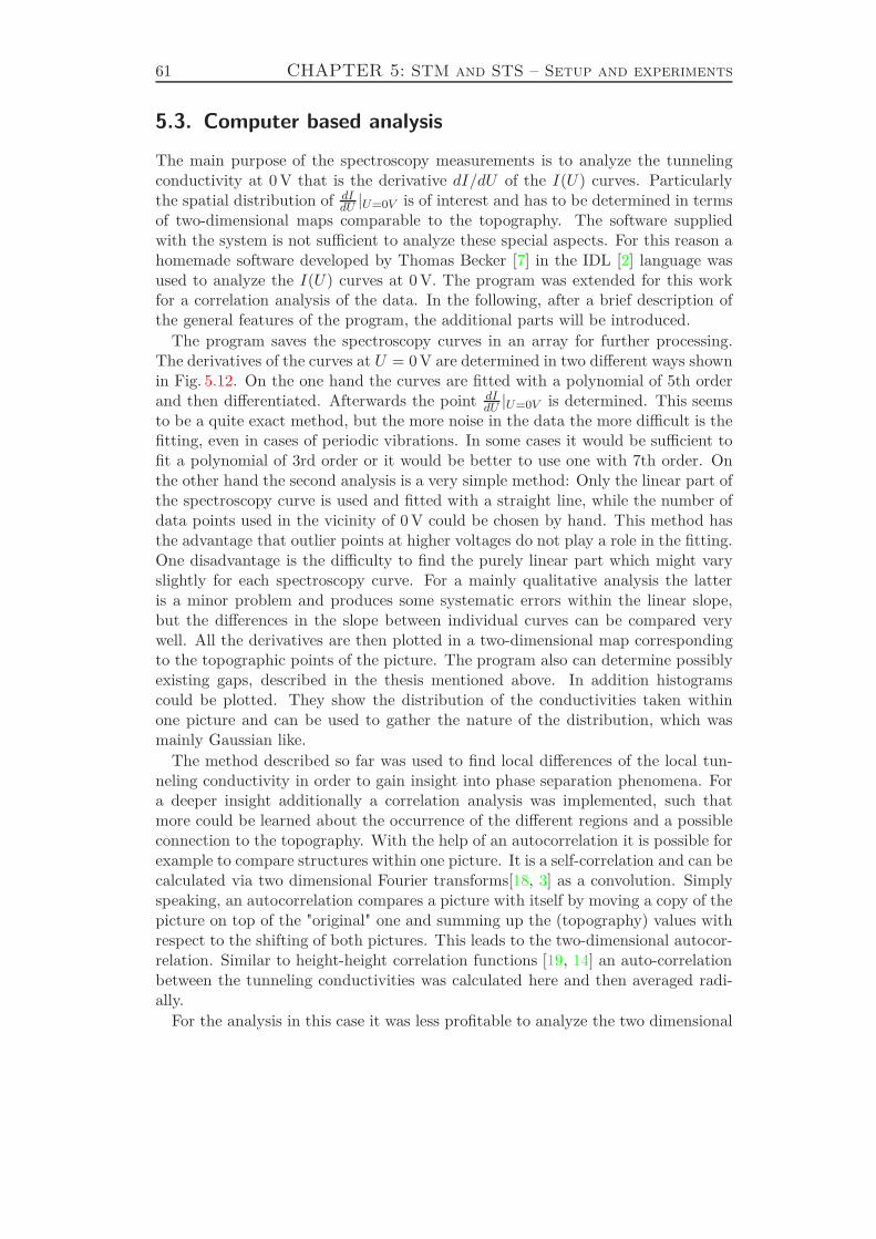
61 CHAPTER 5: STM and STS – Setup and experiments
5.3. Computer based analysis
The main purpose of the spectroscopy measurements is to analyze the tunnelingconductivity at 0 V that is the derivative dI/dU of the I(U) curves. Particularlythe spatial distribution of dIdU |U=0V is of interest and has to be determined in termsof two-dimensional maps comparable to the topography. The software suppliedwith the system is not sufficient to analyze these special aspects. For this reason ahomemade software developed by Thomas Becker [7] in the IDL [2] language wasused to analyze the I(U) curves at 0 V. The program was extended for this workfor a correlation analysis of the data. In the following, after a brief description ofthe general features of the program, the additional parts will be introduced.
The program saves the spectroscopy curves in an array for further processing.The derivatives of the curves at U = 0 V are determined in two different ways shownin Fig. 5.12. On the one hand the curves are fitted with a polynomial of 5th orderand then differentiated. Afterwards the point dIdU |U=0V is determined. This seemsto be a quite exact method, but the more noise in the data the more difficult is thefitting, even in cases of periodic vibrations. In some cases it would be sufficient tofit a polynomial of 3rd order or it would be better to use one with 7th order. Onthe other hand the second analysis is a very simple method: Only the linear part ofthe spectroscopy curve is used and fitted with a straight line, while the number ofdata points used in the vicinity of 0 V could be chosen by hand. This method hasthe advantage that outlier points at higher voltages do not play a role in the fitting.One disadvantage is the difficulty to find the purely linear part which might varyslightly for each spectroscopy curve. For a mainly qualitative analysis the latteris a minor problem and produces some systematic errors within the linear slope,but the differences in the slope between individual curves can be compared verywell. All the derivatives are then plotted in a two-dimensional map correspondingto the topographic points of the picture. The program also can determine possiblyexisting gaps, described in the thesis mentioned above. In addition histogramscould be plotted. They show the distribution of the conductivities taken withinone picture and can be used to gather the nature of the distribution, which wasmainly Gaussian like.
The method described so far was used to find local differences of the local tun-neling conductivity in order to gain insight into phase separation phenomena. Fora deeper insight additionally a correlation analysis was implemented, such thatmore could be learned about the occurrence of the different regions and a possibleconnection to the topography. With the help of an autocorrelation it is possible forexample to compare structures within one picture. It is a self-correlation and can becalculated via two dimensional Fourier transforms[18, 3] as a convolution. Simplyspeaking, an autocorrelation compares a picture with itself by moving a copy of thepicture on top of the "original" one and summing up the (topography) values withrespect to the shifting of both pictures. This leads to the two-dimensional autocor-relation. Similar to height-height correlation functions [19, 14] an auto-correlationbetween the tunneling conductivities was calculated here and then averaged radi-ally.
For the analysis in this case it was less profitable to analyze the two dimensional
5.3. Computer based analysis 62
-0.4 -0.2 0.0 0.2 0.4
-0.2
-0.1
0.0
0.1
0.2
0.3I [
nA]
U [V]
Single I(U) curve Polynomial Fit, 5th order
-0.4 -0.2 0.0 0.2 0.4
-0.2
-0.1
0.0
0.1
0.2
0.3
0.4
I [nA
]
U [V]
Single I(V) curve Linear fit, middle part
Figure 5.12.: Fitting example for a single I(U) curve with a polynomial of 5th order (left) anda line for the linear part (right).
correlation maps. They show changes of the regular structure, including the con-tained tip structure, but the determination of relevant length scales is inefficient.Due to this fact the radially averaged autocorrelation function, C(r), is calculated.The radii r are computed in terms of pixel integer values and for the final radialcorrelation function the pixel radii are converted into the topographic scale in nm.The correlation functions then are normalized, while a mean value was subtractedbefore from the uncorrelated two-dimensional maps to eliminate plane effects. Toshow an example the test pictures in Fig. 5.13 were drawn and saved in the formatof the microscope program, such that they could be analyzed in the same way asmeasured data. The respective two-dimensional autocorrelation image is presentedin the lower left of Fig. 5.13. The radial autocorrelation function is demonstratedin Fig. 5.14.
For the size analysis only empirical formalisms can be used. Since it does not yieldexact length scales it is mostly important to analyze the radial correlation curvesconsistently. There are three features, which might be evaluated, that is the firstdecay, the first minimum and the first maximum of C(r). Intuitively the first decayis related to the dimensions of corresponding structures (the correlation decreaseswith further shifting of the pictures). In the same way the first minimum mightbe interpreted of a mean corresponding to the largest dimensions of the existingstructures (where the concurrence is minimal) and the first maximum occurs on alength comparable to the distance between regularly distributed objects. If there isno periodicity of the occurrence of structures (i.e. there is no distinctive distance)no maximum will occur. Often the first decay length, also called the correlationlength, is determined as the radius rl at which the normalized correlation Cnorm(r)is decreased to 1/e by fitting a simple exponential function y = A ·exp (−r/rl)+y0.
To demonstrate the effect of noise, which is always present in measurements,some artificial noise was added to the test picture (Fig. 5.13 upper right). Due tothe noise the analysis does not find any correlation between neighboring pixels,which appears as the steep decay at the smallest radii (Fig. 5.14 a), whereat thestructure of the curve remains the same. The latter problem can be solved by
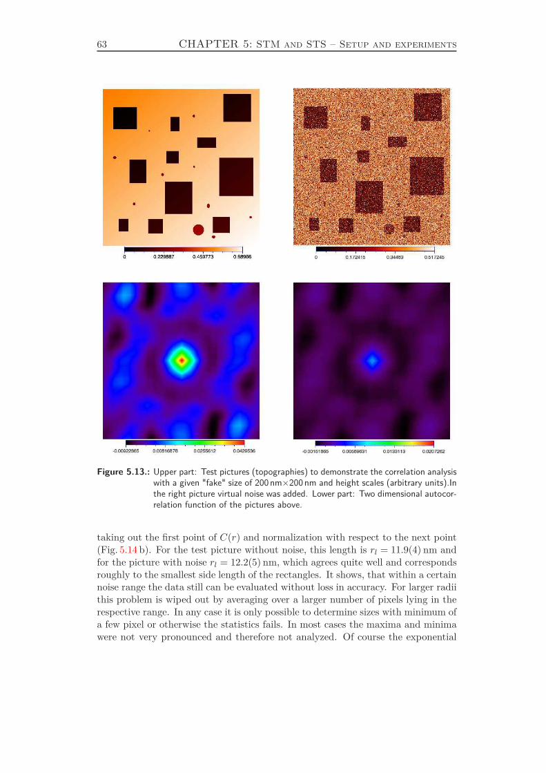
63 CHAPTER 5: STM and STS – Setup and experiments
Figure 5.13.: Upper part: Test pictures (topographies) to demonstrate the correlation analysiswith a given "fake" size of 200 nm×200 nm and height scales (arbitrary units).Inthe right picture virtual noise was added. Lower part: Two dimensional autocor-relation function of the pictures above.
taking out the first point of C(r) and normalization with respect to the next point(Fig. 5.14 b). For the test picture without noise, this length is rl = 11.9(4) nm andfor the picture with noise rl = 12.2(5) nm, which agrees quite well and correspondsroughly to the smallest side length of the rectangles. It shows, that within a certainnoise range the data still can be evaluated without loss in accuracy. For larger radiithis problem is wiped out by averaging over a larger number of pixels lying in therespective range. In any case it is only possible to determine sizes with minimum ofa few pixel or otherwise the statistics fails. In most cases the maxima and minimawere not very pronounced and therefore not analyzed. Of course the exponential
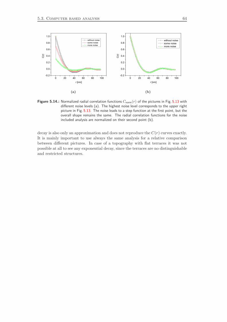
5.3. Computer based analysis 64
0 20 40 60 80 100-0.2
0.0
0.2
0.4
0.6
0.8
1.0
C(r)
r [nm]
without noise some noise more noise
(a)
0 20 40 60 80 100-0.2
0.0
0.2
0.4
0.6
0.8
1.0
C(r)
r [nm]
without noise some noise more noise
(b)
Figure 5.14.: Normalized radial correlation functions Cnorm(r) of the pictures in Fig. 5.13 withdifferent noise levels (a). The highest noise level corresponds to the upper rightpicture in Fig. 5.13. The noise leads to a step function at the first point, but theoverall shape remains the same. The radial correlation functions for the noiseincluded analysis are normalized on their second point (b).
decay is also only an approximation and does not reproduce the C(r) curves exactly.It is mainly important to use always the same analysis for a relative comparisonbetween different pictures. In case of a topography with flat terraces it was notpossible at all to see any exponential decay, since the terraces are no distinguishableand restricted structures.
65 Bibliography
Bibliography
[1] DORMA Hüppe Raumtrennsysteme GmbH, Westerstede/Ocholt, Deutsch-land.
[2] IDL – Interactive data language. Research Systems, Inc. Version 6.0.
[3] IDL – Reference guide. Technical report, Research Systems, inc., 1998.
[4] Pico - the omicron nanotechnology newsletter. Technical report, Omicron,December 2003.
[5] Teragon’s summary of cryogen properties.http://www.trgn.com/database/cryogen.html, February 2005. TeragonResearch, San Francisco, CA.
[6] N. H. Balshaw. Practical cryogenics. Technical report, Oxford InstrumentsSuperconductivity Limited, 2001.
[7] T. Becker. Untersuchung der elektrischen Phasenseparation in dünnen Man-
ganatschichten mit Rastersondenspektroskopie. Doktorarbeit, Universität Göt-tingen, 2004.
[8] T. Becker, C. Streng, Y. Luo, V. Moshnyaga, B. Damaschke, N. Shannon, andK. Samwer. Phys. Rev. Lett., 89:2372038, 2002.
[9] Dawn. A. Bonnell, editor. Scanning Tunneling Microscopy and Spectroscopy.VCH Publishers, Inc., 1993.
[10] C. Julian Chen. Introduction to Scanning Tunneling Microscopy. Oxford Uni-versity Press, 1993.
[11] C. Enss and S. Hunklinger. Tieftemperaturphysik. Springer-Verlag, Berlin,2000.
[12] D. Frickel. Omicron nanotechnologies, Personal communication.
[13] David R. Lide, editor. CRC Handbook of Chemistry and Physics. CRC Press.Boca Raton, Florida, 2003.
[14] S. G. Mayr. Oberflächenrauigkeit von amorphen ZrAlCu-Schichten. Diplomar-beit, Universität Augsburg, 1997.
[15] M. Okano, K. Kajimura, S. Wakiyama, F. Sakai, W. Mizutani, and M. Ono.J. Vac. Sci. Technol. A, A5:3313, 1987.
[16] Omicron Nanotechnology. Cryogenic SFM: User’s Guide and Service Manual,2001.
[17] Oxford Instruments. Operator’s handbook: Spectromag SFM, February 2003.

Bibliography 66
[18] W. H. Press, S. A. Teukolsky, W. T. Vetterling, and B. P. Flannery. Numerical
Recipes in C. Cambridge University Press, 1992.
[19] B. M. Reinker. STM-Untersuchungen an amorphen ZrCo- und CrAlCu-
Aufdampfschichten. Doktorarbeit, Universität Augsburg, 1997.
[20] U. Tietze and Ch. Schenk. Halbleiter-Schaltungstechnik. Springer Verlag, 1971.
[21] L. E. C. van de Leemput and H. van Kempen. Rep. Prog. Phys., 55:1165,1992.
[22] W. Wulfhekel. Personal communication.
[23] M. Wutz, H. Adam, and W. Walcher. Theorie und Praxis der Vakuumtechnik.Friedr. Vieweg & Sohn Verlagsgesellschaft mbH, Braunschweig, 1988.
6. The basic sample properties
Different films of La0.75Ca0.25MnO3 were prepared by the MAD technique (Chap. 4.1)on MgO(100) substrates. By varying the deposition parameters (see detailed dataApp. A), different growth modes were observed, that is from a grain like (3D)growth to a layer-by-layer (LL) growth. The films differed slightly in their generalproperties like the microscopic structure, the resistivity and the metal-insulatortransition temperature, but the sharpness of the MIT varies with the differencesin structure. Expressing the growth modes either a grainy surface or flat terraceswere observed by STM measurements. In other words a different degree of latticedistortions and ordering in the samples could be accounted for the different growthconditions. The varying microstructures play a crucial role in the magnetic andelectronic properties in manganites [9], being rooted in the exchange mechanismswhich rely sensitively on bond angles and distortions (Chap. 2). An evolution withrespect to the ordering in dependence on the growth modes was observed for aseries of films. It was impossible to investigate all these films with STS, but theoverall structural and other general properties are important in order to put theused films into a more general perspective. In a sample series even a cation order-ing on the A-site as the "top end" of stringent ordering was observed by HRTEMpictures [6] and STM investigations on atomic scale [8]. In this case not only aperfectly oriented crystal lattice, but also an ordering of the ions evokes the sharpand pronounced MIT.
In this chapter the structural and commonly measured standard properties willbe given to summarize the sample characteristics. These results are essential tounderstand the microstructure and hence the following results of the electronicproperties, which are observed on a microscopic scale by the STS measurements.There are different models to explain the MIT and its mechanism, but they canonly be discussed knowing the microstructure of the samples. There might bedifferences due to not perfectly built samples, that is, some effects might arise fromextrinsic effects like structural irregularities [1, 10, 9] caused by lattice strain fromthe substrates, grains in different orientations, oxygen content, etc. Since it istherefore in general difficult to produce perfect manganite samples and especiallythin films, the latter effects have to be considered in a discussion of the electronicmechanisms.
6.1. Growth mode
As a starting point the topographies from two of the differently prepared films givean impression about the structural sensitiveness in relation to the deposition con-ditions. These differences can be ascribed mainly to the different deposition rates,which were 0.64 ml/min (precurser solution per time) for the 3D and 0.125 ml/min
67
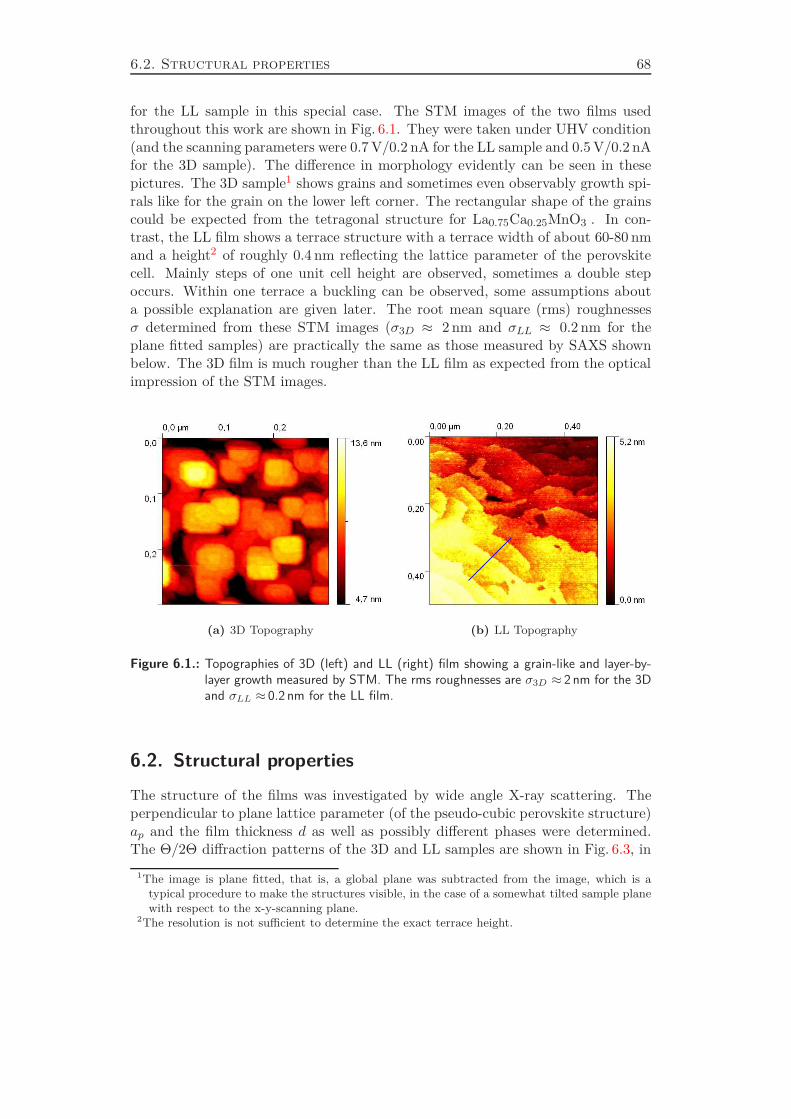
6.2. Structural properties 68
for the LL sample in this special case. The STM images of the two films usedthroughout this work are shown in Fig. 6.1. They were taken under UHV condition(and the scanning parameters were 0.7 V/0.2 nA for the LL sample and 0.5 V/0.2 nAfor the 3D sample). The difference in morphology evidently can be seen in thesepictures. The 3D sample1 shows grains and sometimes even observably growth spi-rals like for the grain on the lower left corner. The rectangular shape of the grainscould be expected from the tetragonal structure for La0.75Ca0.25MnO3 . In con-trast, the LL film shows a terrace structure with a terrace width of about 60-80 nmand a height2 of roughly 0.4 nm reflecting the lattice parameter of the perovskitecell. Mainly steps of one unit cell height are observed, sometimes a double stepoccurs. Within one terrace a buckling can be observed, some assumptions abouta possible explanation are given later. The root mean square (rms) roughnessesσ determined from these STM images (σ3D ≈ 2 nm and σLL ≈ 0.2 nm for theplane fitted samples) are practically the same as those measured by SAXS shownbelow. The 3D film is much rougher than the LL film as expected from the opticalimpression of the STM images.
(a) 3D Topography (b) LL Topography
Figure 6.1.: Topographies of 3D (left) and LL (right) film showing a grain-like and layer-by-layer growth measured by STM. The rms roughnesses are σ3D ≈ 2 nm for the 3Dand σLL ≈ 0.2 nm for the LL film.
6.2. Structural properties
The structure of the films was investigated by wide angle X-ray scattering. Theperpendicular to plane lattice parameter (of the pseudo-cubic perovskite structure)ap and the film thickness d as well as possibly different phases were determined.The Θ/2Θ diffraction patterns of the 3D and LL samples are shown in Fig. 6.3, in
1The image is plane fitted, that is, a global plane was subtracted from the image, which is atypical procedure to make the structures visible, in the case of a somewhat tilted sample planewith respect to the x-y-scanning plane.
2The resolution is not sufficient to determine the exact terrace height.
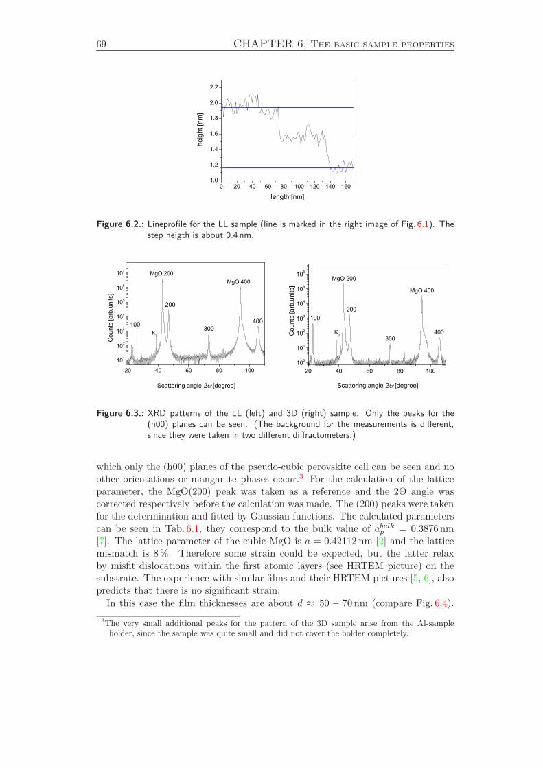
69 CHAPTER 6: The basic sample properties
0 20 40 60 80 100 120 140 1601.0
1.2
1.4
1.6
1.8
2.0
2.2
heig
ht [n
m]
length [nm]
Figure 6.2.: Lineprofile for the LL sample (line is marked in the right image of Fig. 6.1). Thestep heigth is about 0.4 nm.
20 40 60 80 100
101
102
103
104
105
106
107
100 400300
MgO 400
Cou
nts
[arb
.uni
ts]
Scattering angle 2 [degree]
Kβ
MgO 200
200
20 40 60 80 100100
101
102
103
104
105
106
Cou
nts
[arb
.uni
ts]
Scattering angle 2 [degree]
Kβ 400
300
200100
MgO 400
MgO 200
Figure 6.3.: XRD patterns of the LL (left) and 3D (right) sample. Only the peaks for the(h00) planes can be seen. (The background for the measurements is different,since they were taken in two different diffractometers.)
which only the (h00) planes of the pseudo-cubic perovskite cell can be seen and noother orientations or manganite phases occur.3 For the calculation of the latticeparameter, the MgO(200) peak was taken as a reference and the 2Θ angle wascorrected respectively before the calculation was made. The (200) peaks were takenfor the determination and fitted by Gaussian functions. The calculated parameterscan be seen in Tab. 6.1, they correspond to the bulk value of abulkp = 0.3876 nm[7]. The lattice parameter of the cubic MgO is a = 0.42112 nm [2] and the latticemismatch is 8 %. Therefore some strain could be expected, but the latter relaxby misfit dislocations within the first atomic layers (see HRTEM picture) on thesubstrate. The experience with similar films and their HRTEM pictures [5, 6], alsopredicts that there is no significant strain.
In this case the film thicknesses are about d ≈ 50 − 70 nm (compare Fig. 6.4).
3The very small additional peaks for the pattern of the 3D sample arise from the Al-sampleholder, since the sample was quite small and did not cover the holder completely.
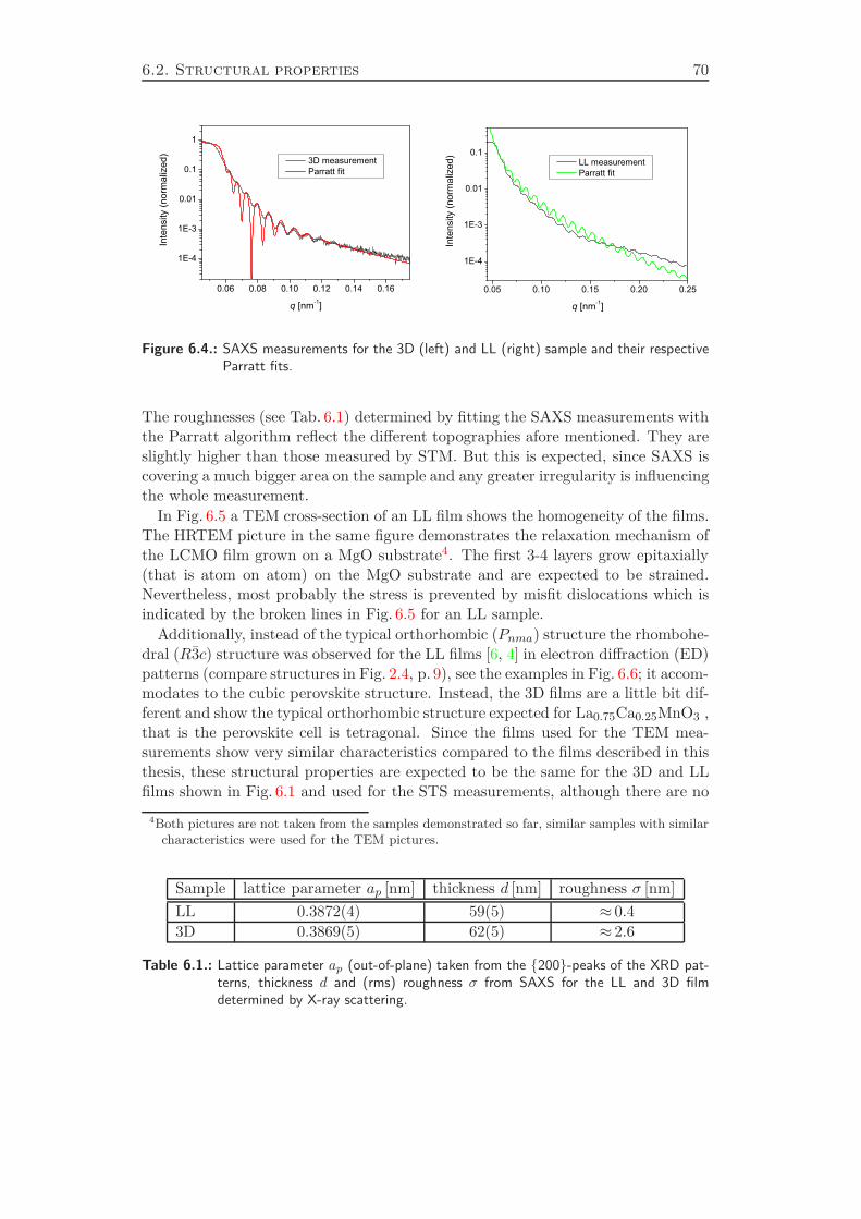
6.2. Structural properties 70
0.06 0.08 0.10 0.12 0.14 0.16
1E-4
1E-3
0.01
0.1
1
Inte
nsity
(nor
mal
ized
)
q [nm-1]
3D measurement Parratt fit
0.05 0.10 0.15 0.20 0.25
1E-4
1E-3
0.01
0.1
Inte
nsity
(nor
mal
ized
)
q [nm-1]
LL measurement Parratt fit
Figure 6.4.: SAXS measurements for the 3D (left) and LL (right) sample and their respectiveParratt fits.
The roughnesses (see Tab. 6.1) determined by fitting the SAXS measurements withthe Parratt algorithm reflect the different topographies afore mentioned. They areslightly higher than those measured by STM. But this is expected, since SAXS iscovering a much bigger area on the sample and any greater irregularity is influencingthe whole measurement.
In Fig. 6.5 a TEM cross-section of an LL film shows the homogeneity of the films.The HRTEM picture in the same figure demonstrates the relaxation mechanism ofthe LCMO film grown on a MgO substrate4. The first 3-4 layers grow epitaxially(that is atom on atom) on the MgO substrate and are expected to be strained.Nevertheless, most probably the stress is prevented by misfit dislocations which isindicated by the broken lines in Fig. 6.5 for an LL sample.
Additionally, instead of the typical orthorhombic (Pnma) structure the rhombohe-dral (R3c) structure was observed for the LL films [6, 4] in electron diffraction (ED)patterns (compare structures in Fig. 2.4, p. 9), see the examples in Fig. 6.6; it accom-modates to the cubic perovskite structure. Instead, the 3D films are a little bit dif-ferent and show the typical orthorhombic structure expected for La0.75Ca0.25MnO3 ,that is the perovskite cell is tetragonal. Since the films used for the TEM mea-surements show very similar characteristics compared to the films described in thisthesis, these structural properties are expected to be the same for the 3D and LLfilms shown in Fig. 6.1 and used for the STS measurements, although there are no
4Both pictures are not taken from the samples demonstrated so far, similar samples with similarcharacteristics were used for the TEM pictures.
Sample lattice parameter ap [nm] thickness d [nm] roughness σ [nm]
LL 0.3872(4) 59(5) ≈ 0.43D 0.3869(5) 62(5) ≈ 2.6
Table 6.1.: Lattice parameter ap (out-of-plane) taken from the 200-peaks of the XRD pat-terns, thickness d and (rms) roughness σ from SAXS for the LL and 3D filmdetermined by X-ray scattering.
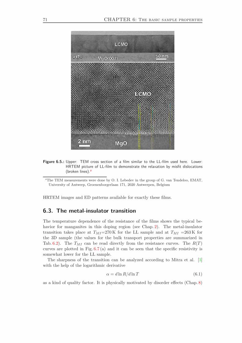
71 CHAPTER 6: The basic sample properties
Figure 6.5.: Upper: TEM cross section of a film similar to the LL-film used here. Lower:HRTEM picture of LL-film to demonstrate the relaxation by misfit dislocations(broken lines).a
aThe TEM measurements were done by O. I. Lebedev in the group of G. van Tendeloo, EMAT,University of Antwerp, Groenenborgerlaan 171, 2020 Antwerpen, Belgium
HRTEM images and ED patterns available for exactly these films.
6.3. The metal-insulator transition
The temperature dependence of the resistance of the films shows the typical be-havior for manganites in this doping region (see Chap. 2). The metal-insulatortransition takes place at TMI=270 K for the LL sample and at TMI =263 K forthe 3D sample (the values for the bulk transport properties are summarized inTab. 6.2). The TMI can be read directly from the resistance curves. The R(T )curves are plotted in Fig. 6.7 (a) and it can be seen that the specific resistivity issomewhat lower for the LL sample.
The sharpness of the transition can be analyzed according to Mitra et al. [3]with the help of the logarithmic derivative
α = d lnR/d ln T (6.1)
as a kind of quality factor. It is physically motivated by disorder effects (Chap. 8)
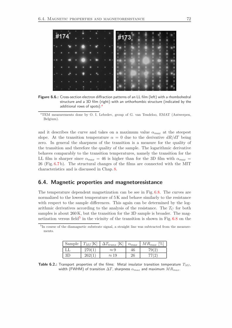
6.4. Magnetic properties and magnetoresistance 72
Figure 6.6.: Cross-section electron diffraction patterns of an LL film (left) with a rhombohedralstructure and a 3D film (right) with an orthorhombic structure (indicated by theadditional rows of spots).a
aTEM measurements done by O. I. Lebedev, group of G. van Tendeloo, EMAT (Antwerpen,Belgium).
and it describes the curve and takes on a maximum value αmax at the steepestslope. At the transition temperature α = 0 due to the derivative dR/dT beingzero. In general the sharpness of the transition is a measure for the quality ofthe transition and therefore the quality of the sample. The logarithmic derivativebehaves comparably to the transition temperatures, namely the transition for theLL film is sharper since αmax = 46 is higher than for the 3D film with αmax =26 (Fig. 6.7 b). The structural changes of the films are connected with the MITcharacteristics and is discussed in Chap. 8.
6.4. Magnetic properties and magnetoresistance
The temperature dependent magnetization can be see in Fig. 6.8. The curves arenormalized to the lowest temperature of 5 K and behave similarly to the resistancewith respect to the sample differences. This again can be determined by the log-arithmic derivatives according to the analysis of the resistance. The TC for bothsamples is about 260 K, but the transition for the 3D sample is broader. The mag-netization versus field5 in the vicinity of the transition is shown in Fig. 6.8 on the
5In course of the diamagnetic substrate signal, a straight line was subtracted from the measure-ments.
Sample TMI [K] ∆Ttrans [K] αmax MRmax [%]
LL 270(1) ≈ 9 46 79(2)3D 262(1) ≈ 19 26 77(2)
Table 6.2.: Transport properties of the films: Metal insulator transition temperature TMI ,width (FWHM) of transition ∆T , sharpness αmax and maximum MRmax.
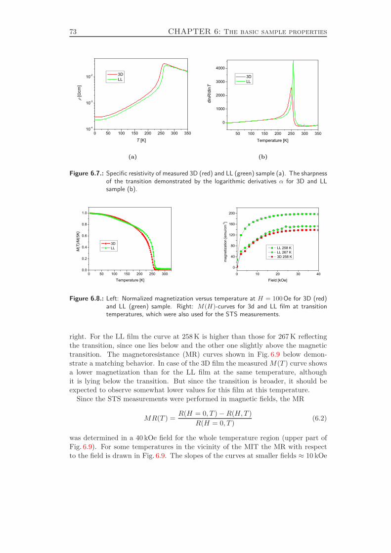
73 CHAPTER 6: The basic sample properties
0 50 100 150 200 250 300 35010-4
10-3
10-2
[Ωcm
]
T [K]
3D LL
(a)
50 100 150 200 250 300 350
0
1000
2000
3000
4000
dlnR
/dlnT
Temperature [K]
3D LL
(b)
Figure 6.7.: Specific resistivity of measured 3D (red) and LL (green) sample (a). The sharpnessof the transition demonstrated by the logarithmic derivatives α for 3D and LLsample (b).
0 50 100 150 200 250 3000.0
0.2
0.4
0.6
0.8
1.0
3D LLM
(T)/M
(5K)
Temperature [K]0 10 20 30 40
0
40
80
120
160
200
mag
netiz
atio
n [e
mu/
cm-3]
Field [kOe]
LL 258 K LL 267 K 3D 258 K
Figure 6.8.: Left: Normalized magnetization versus temperature at H = 100 Oe for 3D (red)and LL (green) sample. Right: M(H)-curves for 3d and LL film at transitiontemperatures, which were also used for the STS measurements.
right. For the LL film the curve at 258 K is higher than those for 267 K reflectingthe transition, since one lies below and the other one slightly above the magnetictransition. The magnetoresistance (MR) curves shown in Fig. 6.9 below demon-strate a matching behavior. In case of the 3D film the measuredM(T ) curve showsa lower magnetization than for the LL film at the same temperature, althoughit is lying below the transition. But since the transition is broader, it should beexpected to observe somewhat lower values for this film at this temperature.
Since the STS measurements were performed in magnetic fields, the MR
MR(T ) =R(H = 0, T )−R(H,T )
R(H = 0, T )(6.2)
was determined in a 40 kOe field for the whole temperature region (upper part ofFig. 6.9). For some temperatures in the vicinity of the MIT the MR with respectto the field is drawn in Fig. 6.9. The slopes of the curves at smaller fields ≈ 10 kOe
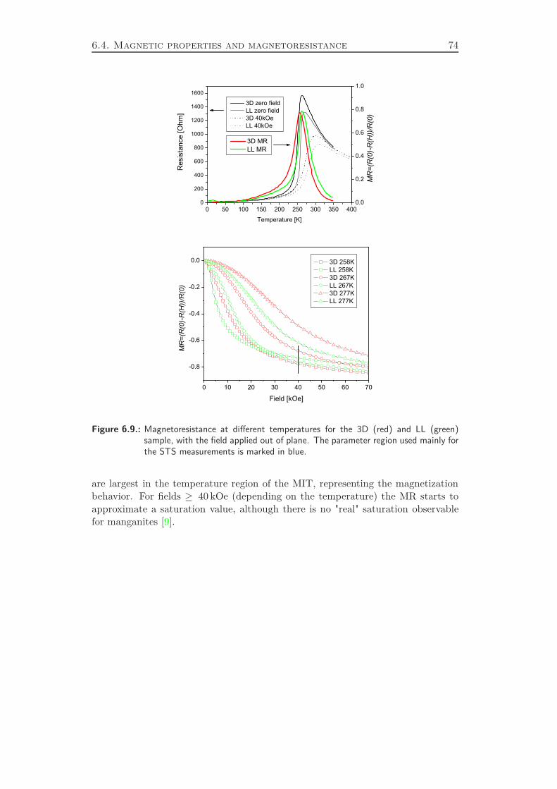
6.4. Magnetic properties and magnetoresistance 74
0 50 100 150 200 250 300 350 4000
200
400
600
800
1000
1200
1400
1600
0.0
0.2
0.4
0.6
0.8
1.0
Res
ista
nce
[Ohm
]
Temperature [K]
3D zero field LL zero field 3D 40kOe LL 40kOe
3D MR LL MR
MR
=(R
(0)-
R(H
))/R
(0)
0 10 20 30 40 50 60 70
-0.8
-0.6
-0.4
-0.2
0.0
MR=(R(0)-R(H
))/R(0)
Field [kOe]
3D 258K LL 258K 3D 267K LL 267K 3D 277K LL 277K
Figure 6.9.: Magnetoresistance at different temperatures for the 3D (red) and LL (green)sample, with the field applied out of plane. The parameter region used mainly forthe STS measurements is marked in blue.
are largest in the temperature region of the MIT, representing the magnetizationbehavior. For fields ≥ 40 kOe (depending on the temperature) the MR starts toapproximate a saturation value, although there is no "real" saturation observablefor manganites [9].

75 Bibliography
Bibliography
[1] B. I. Belevtsev. Low Temp. Phys., 30:421, 2004.
[2] A. Kern, R. Doetyer, and W. Eysel. JCPDS-International Center for Diffrac-tion Data, 1995. MgO, CuKα1 radiation.
[3] J. Mitra, M. Paranjape, A. K. Raychaudhuri, N. D. Mathur, and M. G.Blamire. Phys. Rev. B, 71:094426, 2005.
[4] V. Moshnyaga. Personal communication.
[5] V. Moshnyaga, B. Damaschke, O. Shapoval, A. Belenchuk, J. Faupel, O. I.Lebedev, J. Verbeeck, G. van Tendeloo, M. Müksch, V. Tsurkan, R. Tidecks,and K. Samwer. Nat. Mat., 2:247, 2003.
[6] V. Moshnyaga, L. Sudheendra, O. I. Lebedev, S. A. Köster, K. Gehrke,O. Shapoval, A. Belenchuk, B. Damaschke, G. van Tendeloo, and K. Samwer.Phys. Rev. Lett., 97:107205, 2006.
[7] P. G. Radaelli, G. Iannone, M. Marezio, H. Y. Hwang, S.-W. Cheong, J. D.Jorgensen, and D. N. Argyriou. Phys. Rev. B, 56:8265, 1997.
[8] L. Sudheendra, V. Moshnyaga, E. D. Mishina, B. Damaschke, Th. Rasing, andK. Samwer. Phys. Rev. B, 75:172407, 2007.
[9] Y. Tokura, editor. Colossal magneto-resistive manganites. Gordon and BreachScience Publishers, 2000.
[10] M. Ziese. Rep. Prog. Phys., 56:143, 2002.

Bibliography 76
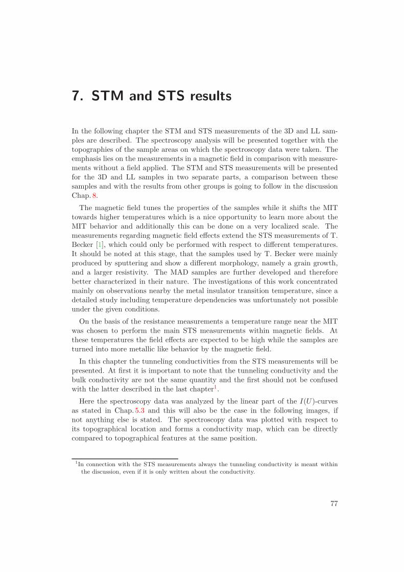
7. STM and STS results
In the following chapter the STM and STS measurements of the 3D and LL sam-ples are described. The spectroscopy analysis will be presented together with thetopographies of the sample areas on which the spectroscopy data were taken. Theemphasis lies on the measurements in a magnetic field in comparison with measure-ments without a field applied. The STM and STS measurements will be presentedfor the 3D and LL samples in two separate parts, a comparison between thesesamples and with the results from other groups is going to follow in the discussionChap. 8.
The magnetic field tunes the properties of the samples while it shifts the MITtowards higher temperatures which is a nice opportunity to learn more about theMIT behavior and additionally this can be done on a very localized scale. Themeasurements regarding magnetic field effects extend the STS measurements of T.Becker [1], which could only be performed with respect to different temperatures.It should be noted at this stage, that the samples used by T. Becker were mainlyproduced by sputtering and show a different morphology, namely a grain growth,and a larger resistivity. The MAD samples are further developed and thereforebetter characterized in their nature. The investigations of this work concentratedmainly on observations nearby the metal insulator transition temperature, since adetailed study including temperature dependencies was unfortunately not possibleunder the given conditions.
On the basis of the resistance measurements a temperature range near the MITwas chosen to perform the main STS measurements within magnetic fields. Atthese temperatures the field effects are expected to be high while the samples areturned into more metallic like behavior by the magnetic field.
In this chapter the tunneling conductivities from the STS measurements will bepresented. At first it is important to note that the tunneling conductivity and thebulk conductivity are not the same quantity and the first should not be confusedwith the latter described in the last chapter1.
Here the spectroscopy data was analyzed by the linear part of the I(U)-curvesas stated in Chap. 5.3 and this will also be the case in the following images, ifnot anything else is stated. The spectroscopy data was plotted with respect toits topographical location and forms a conductivity map, which can be directlycompared to topographical features at the same position.
1In connection with the STS measurements always the tunneling conductivity is meant withinthe discussion, even if it is only written about the conductivity.
77
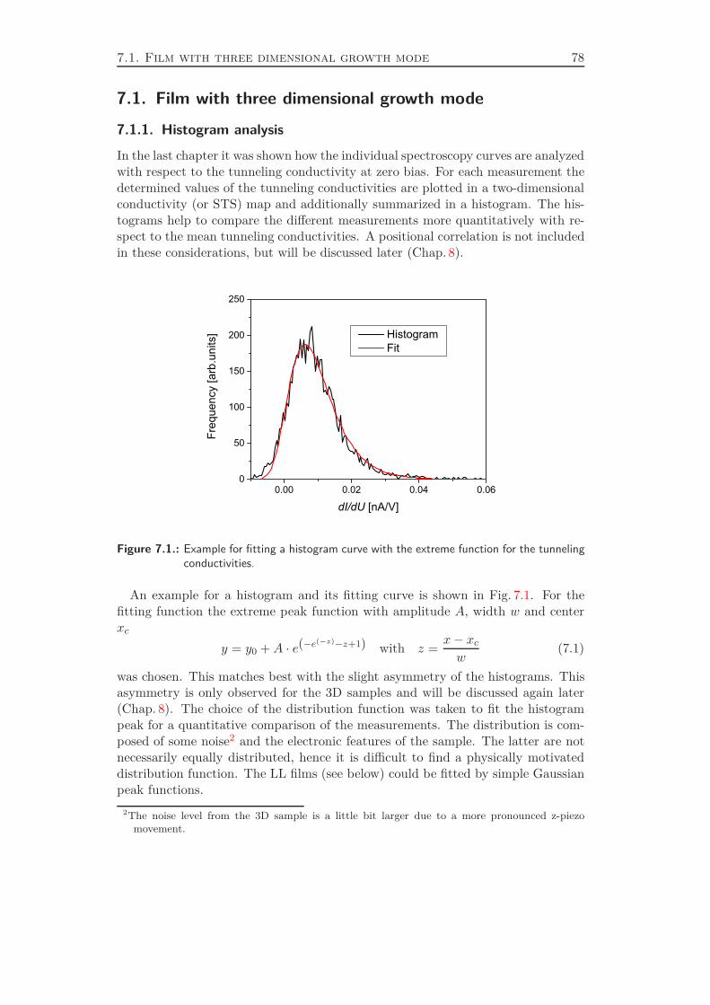
7.1. Film with three dimensional growth mode 78
7.1. Film with three dimensional growth mode
7.1.1. Histogram analysis
In the last chapter it was shown how the individual spectroscopy curves are analyzedwith respect to the tunneling conductivity at zero bias. For each measurement thedetermined values of the tunneling conductivities are plotted in a two-dimensionalconductivity (or STS) map and additionally summarized in a histogram. The his-tograms help to compare the different measurements more quantitatively with re-spect to the mean tunneling conductivities. A positional correlation is not includedin these considerations, but will be discussed later (Chap. 8).
0.00 0.02 0.04 0.060
50
100
150
200
250
Freq
uenc
y [a
rb.u
nits
]
dI/dU [nA/V]
Histogram Fit
Figure 7.1.: Example for fitting a histogram curve with the extreme function for the tunnelingconductivities.
An example for a histogram and its fitting curve is shown in Fig. 7.1. For thefitting function the extreme peak function with amplitude A, width w and centerxc
y = y0 +A · e(−e(−z)−z+1) with z =x− xcw
(7.1)
was chosen. This matches best with the slight asymmetry of the histograms. Thisasymmetry is only observed for the 3D samples and will be discussed again later(Chap. 8). The choice of the distribution function was taken to fit the histogrampeak for a quantitative comparison of the measurements. The distribution is com-posed of some noise2 and the electronic features of the sample. The latter are notnecessarily equally distributed, hence it is difficult to find a physically motivateddistribution function. The LL films (see below) could be fitted by simple Gaussianpeak functions.
2The noise level from the 3D sample is a little bit larger due to a more pronounced z-piezomovement.
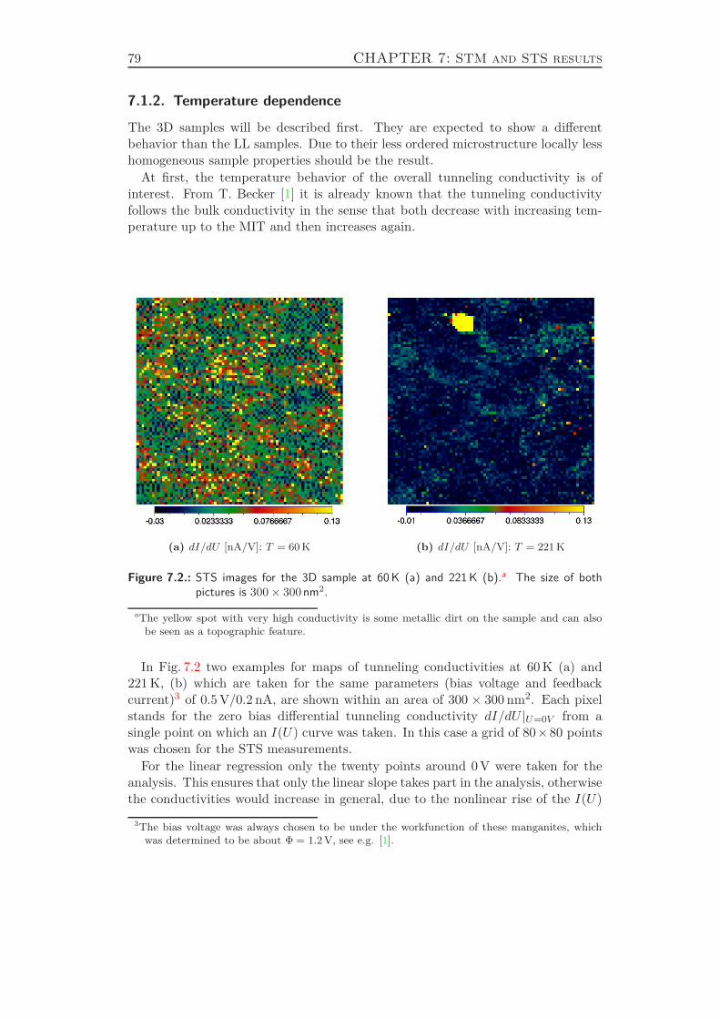
79 CHAPTER 7: STM and STS results
7.1.2. Temperature dependence
The 3D samples will be described first. They are expected to show a differentbehavior than the LL samples. Due to their less ordered microstructure locally lesshomogeneous sample properties should be the result.
At first, the temperature behavior of the overall tunneling conductivity is ofinterest. From T. Becker [1] it is already known that the tunneling conductivityfollows the bulk conductivity in the sense that both decrease with increasing tem-perature up to the MIT and then increases again.
(a) dI/dU [nA/V]: T = 60 K (b) dI/dU [nA/V]: T = 221 K
Figure 7.2.: STS images for the 3D sample at 60 K (a) and 221 K (b).a The size of bothpictures is 300× 300 nm2.
aThe yellow spot with very high conductivity is some metallic dirt on the sample and can alsobe seen as a topographic feature.
In Fig. 7.2 two examples for maps of tunneling conductivities at 60 K (a) and221 K, (b) which are taken for the same parameters (bias voltage and feedbackcurrent)3 of 0.5 V/0.2 nA, are shown within an area of 300 × 300 nm2. Each pixelstands for the zero bias differential tunneling conductivity dI/dU |U=0V from asingle point on which an I(U) curve was taken. In this case a grid of 80×80 pointswas chosen for the STS measurements.
For the linear regression only the twenty points around 0 V were taken for theanalysis. This ensures that only the linear slope takes part in the analysis, otherwisethe conductivities would increase in general, due to the nonlinear rise of the I(U)
3The bias voltage was always chosen to be under the workfunction of these manganites, whichwas determined to be about Φ = 1.2 V, see e.g. [1].
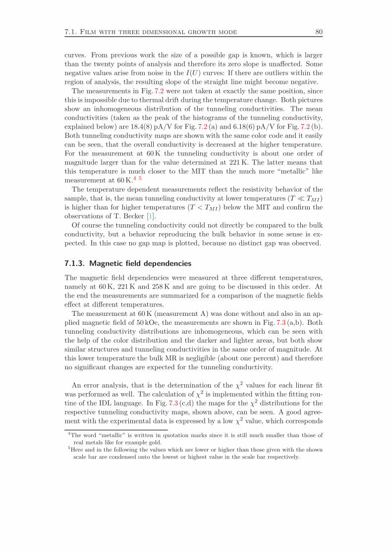
7.1. Film with three dimensional growth mode 80
curves. From previous work the size of a possible gap is known, which is largerthan the twenty points of analysis and therefore its zero slope is unaffected. Somenegative values arise from noise in the I(U) curves: If there are outliers within theregion of analysis, the resulting slope of the straight line might become negative.
The measurements in Fig. 7.2 were not taken at exactly the same position, sincethis is impossible due to thermal drift during the temperature change. Both picturesshow an inhomogeneous distribution of the tunneling conductivities. The meanconductivities (taken as the peak of the histograms of the tunneling conductivity,explained below) are 18.4(8) pA/V for Fig. 7.2 (a) and 6.18(6) pA/V for Fig. 7.2 (b).Both tunneling conductivity maps are shown with the same color code and it easilycan be seen, that the overall conductivity is decreased at the higher temperature.For the measurement at 60 K the tunneling conductivity is about one order ofmagnitude larger than for the value determined at 221 K. The latter means thatthis temperature is much closer to the MIT than the much more “metallic” likemeasurement at 60 K.4 5
The temperature dependent measurements reflect the resistivity behavior of thesample, that is, the mean tunneling conductivity at lower temperatures (T ≪ TMI)is higher than for higher temperatures (T < TMI) below the MIT and confirm theobservations of T. Becker [1].
Of course the tunneling conductivity could not directly be compared to the bulkconductivity, but a behavior reproducing the bulk behavior in some sense is ex-pected. In this case no gap map is plotted, because no distinct gap was observed.
7.1.3. Magnetic field dependencies
The magnetic field dependencies were measured at three different temperatures,namely at 60 K, 221 K and 258 K and are going to be discussed in this order. Atthe end the measurements are summarized for a comparison of the magnetic fieldseffect at different temperatures.
The measurement at 60 K (measurement A) was done without and also in an ap-plied magnetic field of 50 kOe, the measurements are shown in Fig. 7.3 (a,b). Bothtunneling conductivity distributions are inhomogeneous, which can be seen withthe help of the color distribution and the darker and lighter areas, but both showsimilar structures and tunneling conductivities in the same order of magnitude. Atthis lower temperature the bulk MR is negligible (about one percent) and thereforeno significant changes are expected for the tunneling conductivity.
An error analysis, that is the determination of the χ2 values for each linear fitwas performed as well. The calculation of χ2 is implemented within the fitting rou-tine of the IDL language. In Fig. 7.3 (c,d) the maps for the χ2 distributions for therespective tunneling conductivity maps, shown above, can be seen. A good agree-ment with the experimental data is expressed by a low χ2 value, which corresponds
4The word “metallic” is written in quotation marks since it is still much smaller than those ofreal metals like for example gold.
5Here and in the following the values which are lower or higher than those given with the shownscale bar are condensed onto the lowest or highest value in the scale bar respectively.
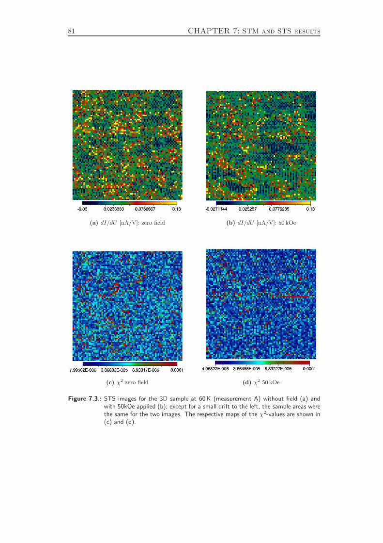
81 CHAPTER 7: STM and STS results
(a) dI/dU [nA/V]: zero field (b) dI/dU [nA/V]: 50 kOe
(c) χ2 zero field (d) χ2 50 kOe
Figure 7.3.: STS images for the 3D sample at 60 K (measurement A) without field (a) andwith 50kOe applied (b); except for a small drift to the left, the sample areas werethe same for the two images. The respective maps of the χ2-values are shown in(c) and (d).
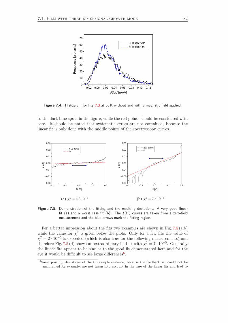
7.1. Film with three dimensional growth mode 82
-0.02 0.00 0.02 0.04 0.06 0.08 0.10 0.120
10
20
30
40
50
60
70
Freq
uenc
y [a
rb.u
nits
]
dI/dU [nA/V]
60K no field 60K 50kOe
Figure 7.4.: Histogram for Fig. 7.3 at 60 K without and with a magnetic field applied.
to the dark blue spots in the figure, while the red points should be considered withcare. It should be noted that systematic errors are not contained, because thelinear fit is only done with the middle points of the spectroscopy curves.
-0.2 -0.1 0.0 0.1 0.2-0.03
-0.02
-0.01
0.00
0.01
0.02
0.03
I [nA
]
U [V]
I(U) curve fit
(a) χ2 = 4.3 10−6
-0.2 -0.1 0.0 0.1 0.2-0.03
-0.02
-0.01
0.00
0.01
0.02
0.03
I [nA
]
U [V]
I(U) curve fit
(b) χ2 = 7.5 10−5
Figure 7.5.: Demonstration of the fitting and the resulting deviations: A very good linearfit (a) and a worst case fit (b). The I(U) curves are taken from a zero-fieldmeasurement and the blue arrows mark the fitting region.
For a better impression about the fits two examples are shown in Fig. 7.5 (a,b)while the value for χ2 is given below the plots. Only for a few fits the value ofχ2 = 2 · 10−5 is exceeded (which is also true for the following measurements) andtherefore Fig. 7.5 (d) shows an extraordinary bad fit with χ2 = 7 · 10−5. Generallythe linear fits appear to be similar to the good fit demonstrated here and for theeye it would be difficult to see large differences6.
6Some possibly deviations of the tip sample distance, because the feedback set could not bemaintained for example, are not taken into account in the case of the linear fits and lead to
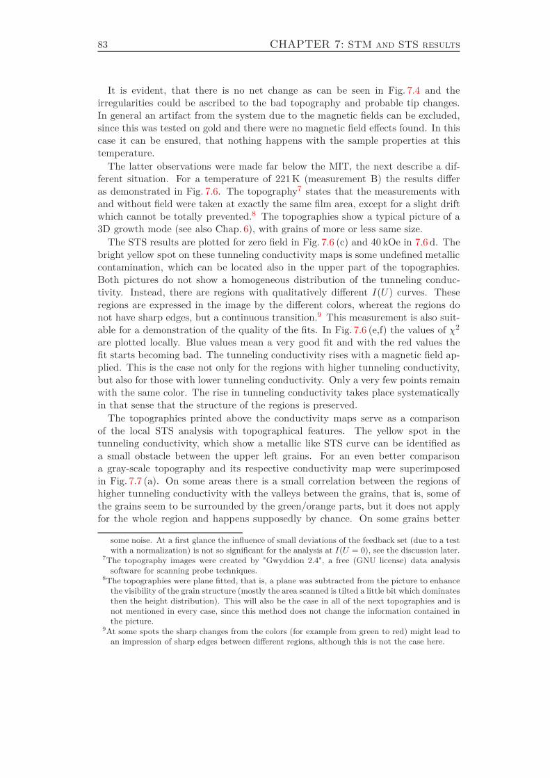
83 CHAPTER 7: STM and STS results
It is evident, that there is no net change as can be seen in Fig. 7.4 and theirregularities could be ascribed to the bad topography and probable tip changes.In general an artifact from the system due to the magnetic fields can be excluded,since this was tested on gold and there were no magnetic field effects found. In thiscase it can be ensured, that nothing happens with the sample properties at thistemperature.
The latter observations were made far below the MIT, the next describe a dif-ferent situation. For a temperature of 221 K (measurement B) the results differas demonstrated in Fig. 7.6. The topography7 states that the measurements withand without field were taken at exactly the same film area, except for a slight driftwhich cannot be totally prevented.8 The topographies show a typical picture of a3D growth mode (see also Chap. 6), with grains of more or less same size.
The STS results are plotted for zero field in Fig. 7.6 (c) and 40 kOe in 7.6 d. Thebright yellow spot on these tunneling conductivity maps is some undefined metalliccontamination, which can be located also in the upper part of the topographies.Both pictures do not show a homogeneous distribution of the tunneling conduc-tivity. Instead, there are regions with qualitatively different I(U) curves. Theseregions are expressed in the image by the different colors, whereat the regions donot have sharp edges, but a continuous transition.9 This measurement is also suit-able for a demonstration of the quality of the fits. In Fig. 7.6 (e,f) the values of χ2
are plotted locally. Blue values mean a very good fit and with the red values thefit starts becoming bad. The tunneling conductivity rises with a magnetic field ap-plied. This is the case not only for the regions with higher tunneling conductivity,but also for those with lower tunneling conductivity. Only a very few points remainwith the same color. The rise in tunneling conductivity takes place systematicallyin that sense that the structure of the regions is preserved.
The topographies printed above the conductivity maps serve as a comparisonof the local STS analysis with topographical features. The yellow spot in thetunneling conductivity, which show a metallic like STS curve can be identified asa small obstacle between the upper left grains. For an even better comparisona gray-scale topography and its respective conductivity map were superimposedin Fig. 7.7 (a). On some areas there is a small correlation between the regions ofhigher tunneling conductivity with the valleys between the grains, that is, some ofthe grains seem to be surrounded by the green/orange parts, but it does not applyfor the whole region and happens supposedly by chance. On some grains better
some noise. At a first glance the influence of small deviations of the feedback set (due to a testwith a normalization) is not so significant for the analysis at I(U = 0), see the discussion later.
7The topography images were created by "Gwyddion 2.4", a free (GNU license) data analysissoftware for scanning probe techniques.
8The topographies were plane fitted, that is, a plane was subtracted from the picture to enhancethe visibility of the grain structure (mostly the area scanned is tilted a little bit which dominatesthen the height distribution). This will also be the case in all of the next topographies and isnot mentioned in every case, since this method does not change the information contained inthe picture.
9At some spots the sharp changes from the colors (for example from green to red) might lead toan impression of sharp edges between different regions, although this is not the case here.
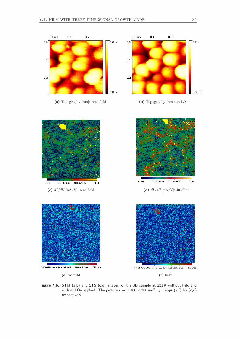
7.1. Film with three dimensional growth mode 84
(a) Topography [nm]: zero field (b) Topography [nm]: 40 kOe
(c) dI/dU [nA/V]: zero field (d) dI/dU [nA/V]: 40 kOe
(e) no field (f) field
Figure 7.6.: STM (a,b) and STS (c,d) images for the 3D sample at 221 K without field andwith 40 kOe applied. The picture size is 300× 300 nm2. χ2 maps (e,f) for (c,d)respectively.
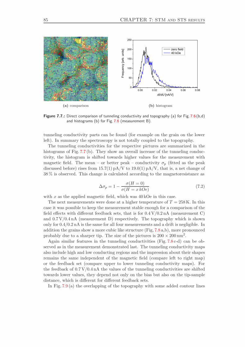
85 CHAPTER 7: STM and STS results
(a) comparison
0.00 0.02 0.04 0.06 0.080
50
100
150
200
250
Freq
uenc
y [a
rb. u
nits
]
dI/dU [nA/V]
zero field 40 kOe
(b) histogram
Figure 7.7.: Direct comparison of tunneling conductivity and topography (a) for Fig. 7.6 (b,d)and histograms (b) for Fig. 7.6 (measurement B).
tunneling conductivity parts can be found (for example on the grain on the lowerleft). In summary the spectroscopy is not totally coupled to the topography.
The tunneling conductivities for the respective pictures are summarized in thehistograms of Fig. 7.7 (b). They show an overall increase of the tunneling conduc-tivity, the histogram is shifted towards higher values for the measurement withmagnetic field. The mean – or better peak – conductivity σp (fitted as the peakdiscussed before) rises from 15.7(1) pA/V to 19.0(1) pA/V, that is, a net change of38 % is observed. This change is calculated according to the magnetoresistance as
∆σp = 1− σ(H = 0)σ(H = x kOe)
(7.2)
with x as the applied magnetic field, which was 40 kOe in this case.The next measurements were done at a higher temperature of T = 258 K. In this
case it was possible to keep the measurement stable enough for a comparison of thefield effects with different feedback sets, that is for 0.4 V/0.2 nA (measurement C)and 0.7 V/0.4 nA (measurement D) respectively. The topography which is shownonly for 0.4/0.2 nA is the same for all four measurements and a drift is negligible. Inaddition the grains show a more cubic like structure (Fig, 7.8 a,b), more pronouncedprobably due to a sharper tip. The size of the pictures is 200× 200 nm2.
Again similar features in the tunneling conductivities (Fig. 7.8 c-d) can be ob-served as in the measurement demonstrated last. The tunneling conductivity mapsalso include high and low conducting regions and the impression about their shapesremains the same independent of the magnetic field (compare left to right map)or the feedback set (compare upper to lower tunneling conductivity maps). Forthe feedback of 0.7 V/0.4 nA the values of the tunneling conductivities are shiftedtowards lower values, they depend not only on the bias but also on the tip-sampledistance, which is different for different feedback sets.
In Fig. 7.9 (a) the overlapping of the topography with some added contour lines
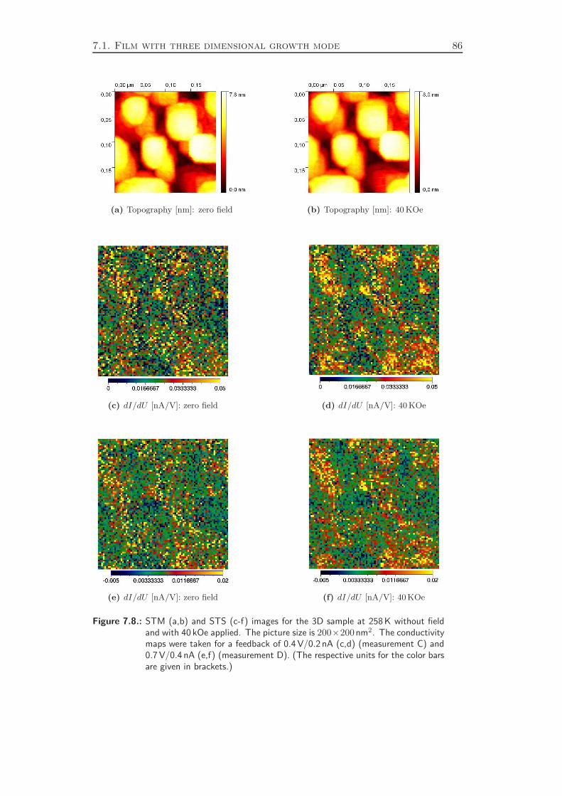
7.1. Film with three dimensional growth mode 86
(a) Topography [nm]: zero field (b) Topography [nm]: 40 KOe
(c) dI/dU [nA/V]: zero field (d) dI/dU [nA/V]: 40 KOe
(e) dI/dU [nA/V]: zero field (f) dI/dU [nA/V]: 40 KOe
Figure 7.8.: STM (a,b) and STS (c-f) images for the 3D sample at 258 K without fieldand with 40 kOe applied. The picture size is 200×200nm2. The conductivitymaps were taken for a feedback of 0.4 V/0.2 nA (c,d) (measurement C) and0.7 V/0.4 nA (e,f) (measurement D). (The respective units for the color barsare given in brackets.)
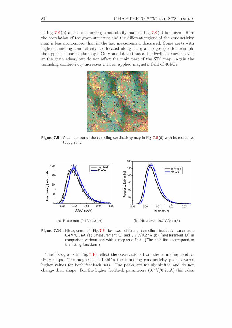
87 CHAPTER 7: STM and STS results
in Fig. 7.8 (b) and the tunneling conductivity map of Fig. 7.8 (d) is shown. Herethe correlation of the grain structure and the different regions of the conductivitymap is less pronounced than in the last measurement discussed. Some parts withhigher tunneling conductivity are located along the grain edges (see for examplethe upper left part of the map). Only small deviations of the feedback current existat the grain edges, but do not affect the main part of the STS map. Again thetunneling conductivity increases with an applied magnetic field of 40 kOe.
Figure 7.9.: A comparison of the tunneling conductivity map in Fig. 7.8 (d) with its respectivetopography.
0.00 0.02 0.04 0.06 0.080
30
60
90
120
Freq
uenc
y [a
rb. u
nits
]
dI/dU [nA/V]
zero field 40 kOe
(a) Histogram (0.4 V/0.2 nA)
-0.01 0.00 0.01 0.02 0.030
50
100
150
200
250
300
Freq
uenc
y [a
rb. u
nits
]
dI/dU [nA/V]
zero field 40 kOe
(b) Histogram (0.7 V/0.4 nA)
Figure 7.10.: Histograms of Fig. 7.8 for two different tunneling feedback parameters0.4 V/0.2 nA (a) (measurement C) and 0.7 V/0.2 nA (b) (measurement D) incomparison without and with a magnetic field. (The bold lines correspond tothe fitting functions.)
The histograms in Fig. 7.10 reflect the observations from the tunneling conduc-tivity maps. The magnetic field shifts the tunneling conductivity peak towardshigher values for both feedback sets. The peaks are mainly shifted and do notchange their shape. For the higher feedback parameters (0.7 V/0.2 nA) this takes
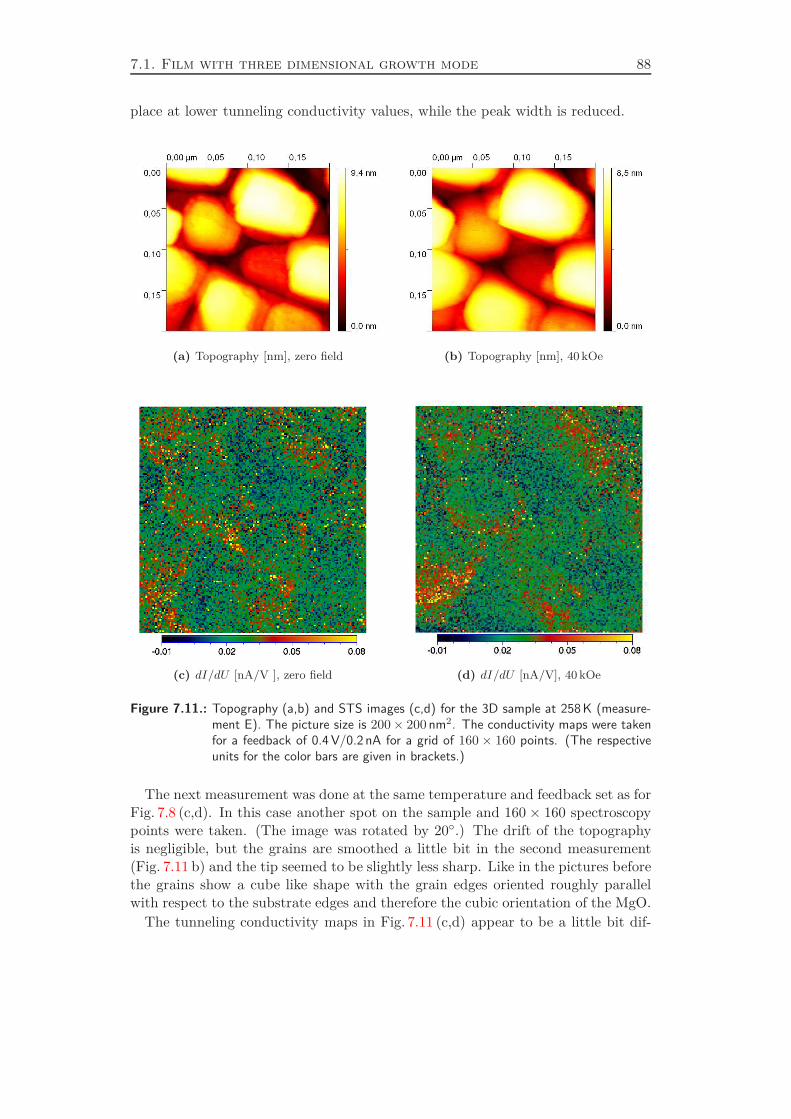
7.1. Film with three dimensional growth mode 88
place at lower tunneling conductivity values, while the peak width is reduced.
(a) Topography [nm], zero field (b) Topography [nm], 40 kOe
(c) dI/dU [nA/V ], zero field (d) dI/dU [nA/V], 40 kOe
Figure 7.11.: Topography (a,b) and STS images (c,d) for the 3D sample at 258 K (measure-ment E). The picture size is 200× 200 nm2. The conductivity maps were takenfor a feedback of 0.4 V/0.2 nA for a grid of 160 × 160 points. (The respectiveunits for the color bars are given in brackets.)
The next measurement was done at the same temperature and feedback set as forFig. 7.8 (c,d). In this case another spot on the sample and 160 × 160 spectroscopypoints were taken. (The image was rotated by 20.) The drift of the topographyis negligible, but the grains are smoothed a little bit in the second measurement(Fig. 7.11 b) and the tip seemed to be slightly less sharp. Like in the pictures beforethe grains show a cube like shape with the grain edges oriented roughly parallelwith respect to the substrate edges and therefore the cubic orientation of the MgO.
The tunneling conductivity maps in Fig. 7.11 (c,d) appear to be a little bit dif-
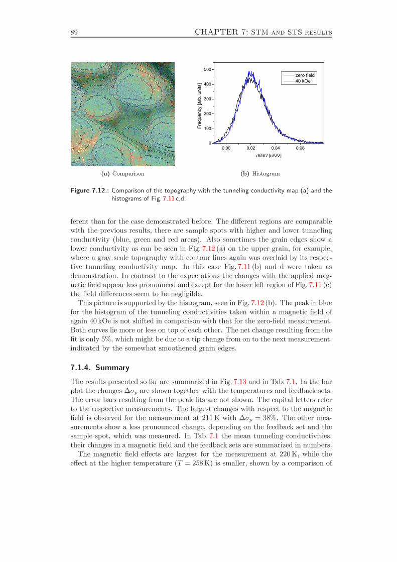
89 CHAPTER 7: STM and STS results
(a) Comparison
0.00 0.02 0.04 0.060
100
200
300
400
500
Freq
uenc
y [a
rb. u
nits
]
dI/dU [nA/V]
zero field 40 kOe
(b) Histogram
Figure 7.12.: Comparison of the topography with the tunneling conductivity map (a) and thehistograms of Fig. 7.11 c,d.
ferent than for the case demonstrated before. The different regions are comparablewith the previous results, there are sample spots with higher and lower tunnelingconductivity (blue, green and red areas). Also sometimes the grain edges show alower conductivity as can be seen in Fig. 7.12 (a) on the upper grain, for example,where a gray scale topography with contour lines again was overlaid by its respec-tive tunneling conductivity map. In this case Fig. 7.11 (b) and d were taken asdemonstration. In contrast to the expectations the changes with the applied mag-netic field appear less pronounced and except for the lower left region of Fig. 7.11 (c)the field differences seem to be negligible.
This picture is supported by the histogram, seen in Fig. 7.12 (b). The peak in bluefor the histogram of the tunneling conductivities taken within a magnetic field ofagain 40 kOe is not shifted in comparison with that for the zero-field measurement.Both curves lie more or less on top of each other. The net change resulting from thefit is only 5%, which might be due to a tip change from on to the next measurement,indicated by the somewhat smoothened grain edges.
7.1.4. Summary
The results presented so far are summarized in Fig. 7.13 and in Tab. 7.1. In the barplot the changes ∆σp are shown together with the temperatures and feedback sets.The error bars resulting from the peak fits are not shown. The capital letters referto the respective measurements. The largest changes with respect to the magneticfield is observed for the measurement at 211 K with ∆σp = 38%. The other mea-surements show a less pronounced change, depending on the feedback set and thesample spot, which was measured. In Tab. 7.1 the mean tunneling conductivities,their changes in a magnetic field and the feedback sets are summarized in numbers.
The magnetic field effects are largest for the measurement at 220 K, while theeffect at the higher temperature (T = 258 K) is smaller, shown by a comparison of
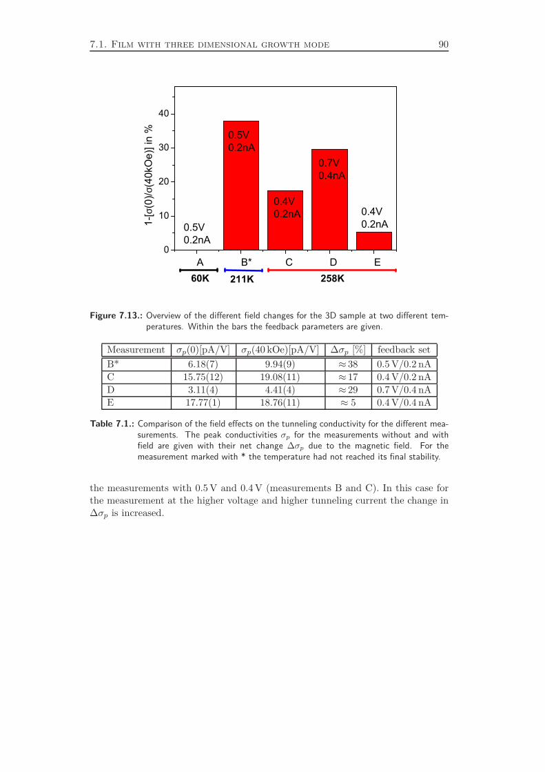
7.1. Film with three dimensional growth mode 90
A B* C D E0
10
20
30
40
60K
0.5V0.2nA
0.7V0.4nA
0.4V0.2nA
0.4V0.2nA
0.5V0.2nA
258K211K
1-[σ
(0)/σ
(40k
Oe)
] in
%
Figure 7.13.: Overview of the different field changes for the 3D sample at two different tem-peratures. Within the bars the feedback parameters are given.
Measurement σp(0)[pA/V] σp(40 kOe)[pA/V] ∆σp [%] feedback set
B* 6.18(7) 9.94(9) ≈ 38 0.5 V/0.2 nAC 15.75(12) 19.08(11) ≈ 17 0.4 V/0.2 nAD 3.11(4) 4.41(4) ≈ 29 0.7 V/0.4 nAE 17.77(1) 18.76(11) ≈ 5 0.4 V/0.4 nA
Table 7.1.: Comparison of the field effects on the tunneling conductivity for the different mea-surements. The peak conductivities σp for the measurements without and withfield are given with their net change ∆σp due to the magnetic field. For themeasurement marked with * the temperature had not reached its final stability.
the measurements with 0.5 V and 0.4 V (measurements B and C). In this case forthe measurement at the higher voltage and higher tunneling current the change in∆σp is increased.
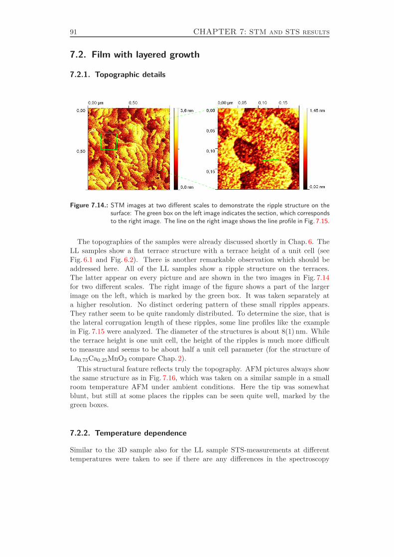
91 CHAPTER 7: STM and STS results
7.2. Film with layered growth
7.2.1. Topographic details
Figure 7.14.: STM images at two different scales to demonstrate the ripple structure on thesurface: The green box on the left image indicates the section, which correspondsto the right image. The line on the right image shows the line profile in Fig. 7.15.
The topographies of the samples were already discussed shortly in Chap. 6. TheLL samples show a flat terrace structure with a terrace height of a unit cell (seeFig. 6.1 and Fig. 6.2). There is another remarkable observation which should beaddressed here. All of the LL samples show a ripple structure on the terraces.The latter appear on every picture and are shown in the two images in Fig. 7.14for two different scales. The right image of the figure shows a part of the largerimage on the left, which is marked by the green box. It was taken separately ata higher resolution. No distinct ordering pattern of these small ripples appears.They rather seem to be quite randomly distributed. To determine the size, that isthe lateral corrugation length of these ripples, some line profiles like the examplein Fig. 7.15 were analyzed. The diameter of the structures is about 8(1) nm. Whilethe terrace height is one unit cell, the height of the ripples is much more difficultto measure and seems to be about half a unit cell parameter (for the structure ofLa0.75Ca0.25MnO3 compare Chap. 2).
This structural feature reflects truly the topography. AFM pictures always showthe same structure as in Fig. 7.16, which was taken on a similar sample in a smallroom temperature AFM under ambient conditions. Here the tip was somewhatblunt, but still at some places the ripples can be seen quite well, marked by thegreen boxes.
7.2.2. Temperature dependence
Similar to the 3D sample also for the LL sample STS-measurements at differenttemperatures were taken to see if there are any differences in the spectroscopy
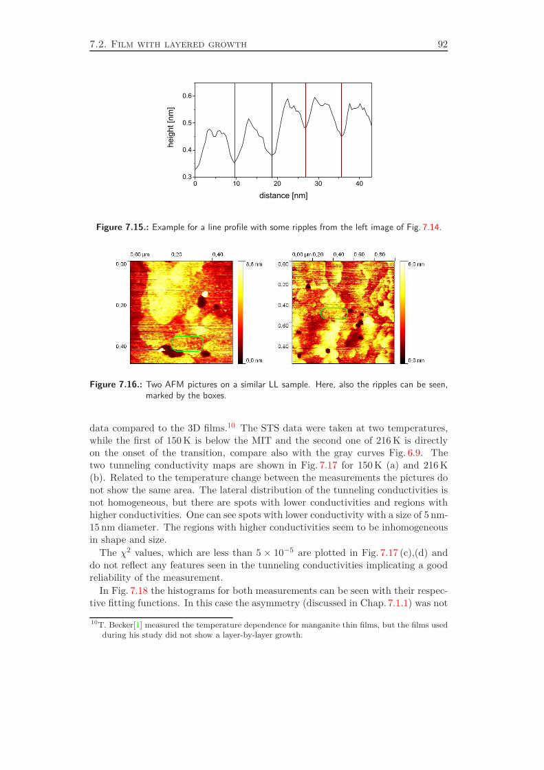
7.2. Film with layered growth 92
0 10 20 30 400.3
0.4
0.5
0.6
heig
ht [n
m]
distance [nm]
Figure 7.15.: Example for a line profile with some ripples from the left image of Fig. 7.14.
Figure 7.16.: Two AFM pictures on a similar LL sample. Here, also the ripples can be seen,marked by the boxes.
data compared to the 3D films.10 The STS data were taken at two temperatures,while the first of 150 K is below the MIT and the second one of 216 K is directlyon the onset of the transition, compare also with the gray curves Fig. 6.9. Thetwo tunneling conductivity maps are shown in Fig. 7.17 for 150 K (a) and 216 K(b). Related to the temperature change between the measurements the pictures donot show the same area. The lateral distribution of the tunneling conductivities isnot homogeneous, but there are spots with lower conductivities and regions withhigher conductivities. One can see spots with lower conductivity with a size of 5 nm-15 nm diameter. The regions with higher conductivities seem to be inhomogeneousin shape and size.
The χ2 values, which are less than 5 × 10⁻⁵ are plotted in Fig. 7.17 (c),(d) anddo not reflect any features seen in the tunneling conductivities implicating a goodreliability of the measurement.
In Fig. 7.18 the histograms for both measurements can be seen with their respec-tive fitting functions. In this case the asymmetry (discussed in Chap. 7.1.1) was not
10T. Becker[1] measured the temperature dependence for manganite thin films, but the films usedduring his study did not show a layer-by-layer growth.
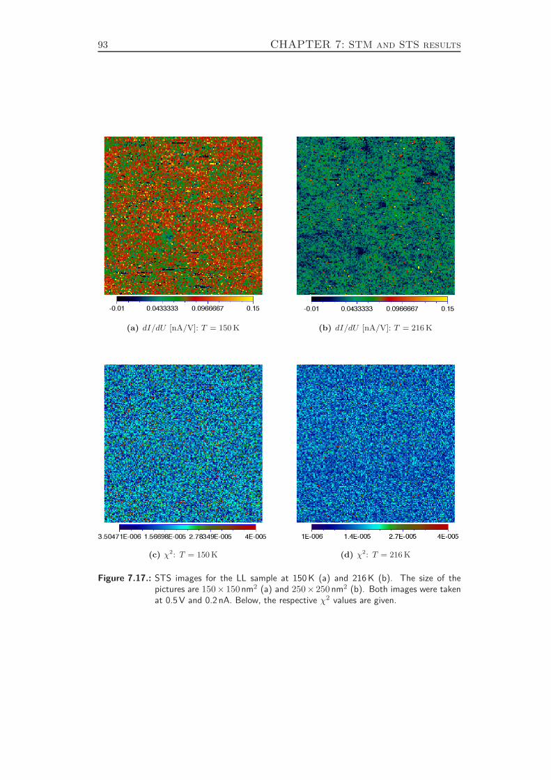
93 CHAPTER 7: STM and STS results
(a) dI/dU [nA/V]: T = 150 K (b) dI/dU [nA/V]: T = 216 K
(c) χ2: T = 150 K (d) χ2: T = 216 K
Figure 7.17.: STS images for the LL sample at 150 K (a) and 216 K (b). The size of thepictures are 150× 150 nm2 (a) and 250× 250 nm2 (b). Both images were takenat 0.5 V and 0.2 nA. Below, the respective χ2 values are given.
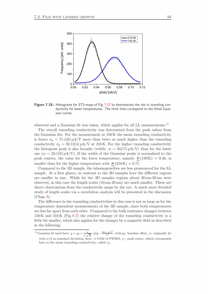
7.2. Film with layered growth 94
0.00 0.02 0.04 0.06 0.08 0.10 0.120
100
200
300
400
500
Freq
uenc
y [a
rb. u
nits
]
dI/dU [nA/V]
215.5K 150.3K
Figure 7.18.: Histograms for STS-maps of Fig. 7.17 to demonstrate the rise in tunneling con-ductivity for lower temperatures. The thick lines correspond to the fitted Gaus-sian curves.
observed and a Gaussian fit was taken, which applies for all LL measurements.11
The overall tunneling conductivity was determined from the peak values fromthe Gaussian fits. For the measurement at 150 K the mean tunneling conductivityis hence σp = 71.1(6) pA/V more than twice as much higher than the tunnelingconductivity σp = 32.12(4) pA/V at 216 K. For the higher tunneling conductivitythe histogram peak is also broader (width: w = 34(17) pA/V) than for the lowerone (w = 23.1(9) pA/V). If the width of the Gaussian peaks is normalized to thepeak centers, the value for the lower temperature, namely w
σp(150 K) = 0.48, is
smaller than for the higher temperature with wσp
(216 K) = 0.71.Compared to the 3D sample, the inhomogeneities are less pronounced for the LL
sample. At a first glance, in contrast to the 3D samples here the different regionsare smaller in size. While for the 3D samples regions about 20 nm-50 nm wereobserved, in this case the length scales (10 nm-20 nm) are much smaller. These aredirect observations from the conductivity maps by the eye. A much more detailedstudy of length scales via a correlation analysis will be presented in the discussion(Chap. 8).
The difference in the tunneling conductivities in this case is not as large as for thetemperature dependent measurements of the 3D sample, since both temperaturesare less far apart from each other. Compared to the bulk resistance changes between150 K and 216 K (Fig. 6.7) the relative change of the tunneling conductivity is alittle bit smaller, which also applies for the changes by a magnetic field as describedin the following.
11Gaussian fit used here: y = y0 + A
w·√π2
· exp− 2(x−xc)2
w2 , with y0: baseline offset, w: originally 2σ
with w/2 as standard deviation, here: ≈ 0.849 of FWHM, xc: peak center, which correspondshere to the mean tunneling conductivity, called σp.
95 CHAPTER 7: STM and STS results
7.2.3. Field dependence
A change of the tunneling conductivities with the temperature was verified in thelast part. Now, the field dependent measurements are presented. For the datacollection the temperature was kept constant while in between two measurementsthe magnetic field was changed. Since the largest effects caused by a magnetic fieldare expected to occur at the MIT (see also Chap. 6, Fig. 6.9), the measurementsconcentrate on temperatures nearby TMI , that is 258 K and 267 K were chosen forthe experiments.
In Fig. 7.19 measurements taken at 258 K are shown. The panels (a) and (b)show the topographies for zero-field and the measurement in a magnetic field. Theimaged area did not change while applying the magnetic field of 40 kOe. Therefore,both tunneling spectroscopy maps can be directly compared with each other. Inthe next row (c,d) the respective tunneling conductivities are shown, taken at a gridof 80× 80 points. The data was collected at a bias voltage of 0.5 V and a feedbackcurrent of 0.2 nA. Some inhomogeneities can be seen also in these conductivitymaps, similar to those shown in Sec. 7.2.2 about the temperature dependency.
Most intriguing is the large color change between the zero-field and the in-fieldmeasurement. The overall tunneling conductivity is shifted towards higher values.The worse conducting parts, that is dark blue areas are shifted and do not remainwith the same tunneling conductivity. On the tunneling conductivity map for thein-field measurement not very many spots with this color can be found, but theregions with lowest tunneling conductivity show a dark green color. The sameaccounts for the higher conducting parts, which are shifted with their tunnelingconductivity as well. For the measurement in a field much more points with redand yellow color appear. In addition a general lateral growth of the areas withhigher tunneling conductivity cannot be found.
In the last row (Fig. 7.19 e,f) the χ2 values are shown and neither do exceed3 · 10−5 nor would give any hints to correlations with the topography. None of thestructures in the tunneling conductivity maps corresponds to any topographicalfeatures like a terrace step or anything else.
The histograms of the tunneling conductivities are plotted in Fig. 7.20 for theanalysis of the mean tunneling conductivities and the distribution of the conductiv-ities. The zero-field and in-field measurements are indicated by the line colors blackand red, respectively, while the thick line is the Gaussian fit for the histograms. Themean tunneling conductivities, determined as the peak centers σp, change about∆σp =45% from σp(0) = 19.26(14)pA/V to σp(40 kOe) = 34.88(15)pA/V while theerror was determined from the Gaussian fitting. The specific values are going to begiven in summary in Tab. 7.2 at the end of this chapter. To set them into relationwith each other again the ratio ∆σp from Eq. 7.2 in Sec. 7.1.3 was used.The width of the peaks increases slightly with the application of the magnetic fieldfrom w = 21.8(4) pA/V to w = 22.3(4) pA/V. The latter will be analyzed in moredetail and compared with the other measurements at the end of this chapter in thesummary.
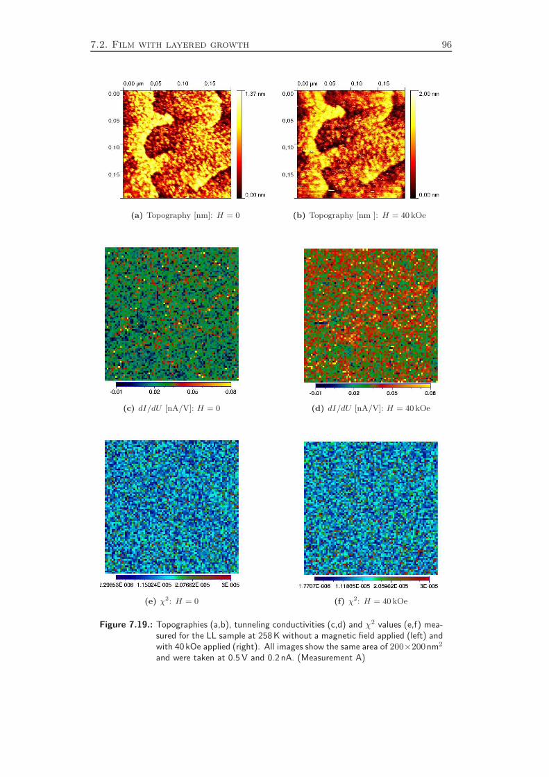
7.2. Film with layered growth 96
(a) Topography [nm]: H = 0 (b) Topography [nm ]: H = 40 kOe
(c) dI/dU [nA/V]: H = 0 (d) dI/dU [nA/V]: H = 40 kOe
(e) χ2: H = 0 (f) χ2: H = 40 kOe
Figure 7.19.: Topographies (a,b), tunneling conductivities (c,d) and χ2 values (e,f) mea-sured for the LL sample at 258 K without a magnetic field applied (left) andwith 40 kOe applied (right). All images show the same area of 200×200nm2
and were taken at 0.5 V and 0.2 nA. (Measurement A)
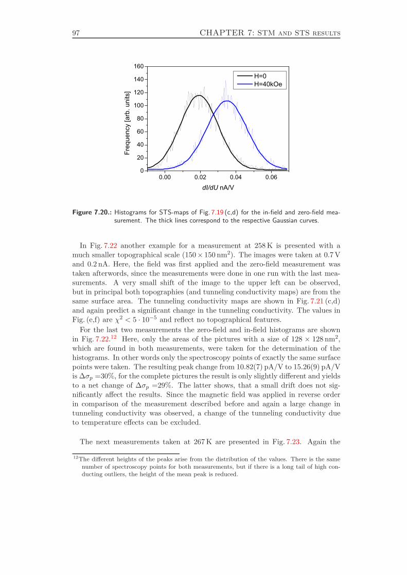
97 CHAPTER 7: STM and STS results
0.00 0.02 0.04 0.060
20
40
60
80
100
120
140
160
Freq
uenc
y [a
rb. u
nits
]
dI/dU nA/V
H=0 H=40kOe
Figure 7.20.: Histograms for STS-maps of Fig. 7.19 (c,d) for the in-field and zero-field mea-surement. The thick lines correspond to the respective Gaussian curves.
In Fig. 7.22 another example for a measurement at 258 K is presented with amuch smaller topographical scale (150× 150 nm2). The images were taken at 0.7 Vand 0.2 nA. Here, the field was first applied and the zero-field measurement wastaken afterwords, since the measurements were done in one run with the last mea-surements. A very small shift of the image to the upper left can be observed,but in principal both topographies (and tunneling conductivity maps) are from thesame surface area. The tunneling conductivity maps are shown in Fig. 7.21 (c,d)and again predict a significant change in the tunneling conductivity. The values inFig. (e,f) are χ2 < 5 · 10−5 and reflect no topographical features.
For the last two measurements the zero-field and in-field histograms are shownin Fig. 7.22.12 Here, only the areas of the pictures with a size of 128 × 128 nm2,which are found in both measurements, were taken for the determination of thehistograms. In other words only the spectroscopy points of exactly the same surfacepoints were taken. The resulting peak change from 10.82(7) pA/V to 15.26(9) pA/Vis ∆σp =30%, for the complete pictures the result is only slightly different and yieldsto a net change of ∆σp =29%. The latter shows, that a small drift does not sig-nificantly affect the results. Since the magnetic field was applied in reverse orderin comparison of the measurement described before and again a large change intunneling conductivity was observed, a change of the tunneling conductivity dueto temperature effects can be excluded.
The next measurements taken at 267 K are presented in Fig. 7.23. Again the
12The different heights of the peaks arise from the distribution of the values. There is the samenumber of spectroscopy points for both measurements, but if there is a long tail of high con-ducting outliers, the height of the mean peak is reduced.
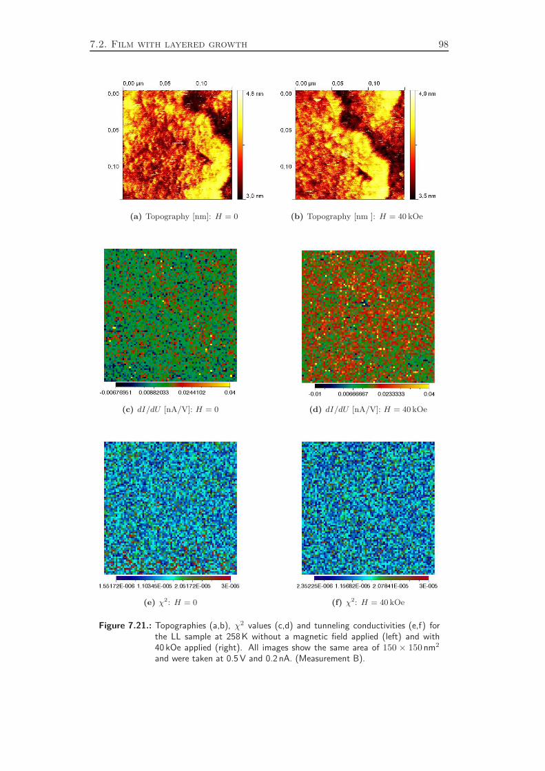
7.2. Film with layered growth 98
(a) Topography [nm]: H = 0 (b) Topography [nm ]: H = 40 kOe
(c) dI/dU [nA/V]: H = 0 (d) dI/dU [nA/V]: H = 40 kOe
(e) χ2: H = 0 (f) χ2: H = 40 kOe
Figure 7.21.: Topographies (a,b), χ2 values (c,d) and tunneling conductivities (e,f) forthe LL sample at 258 K without a magnetic field applied (left) and with40 kOe applied (right). All images show the same area of 150 × 150 nm2
and were taken at 0.5 V and 0.2 nA. (Measurement B).
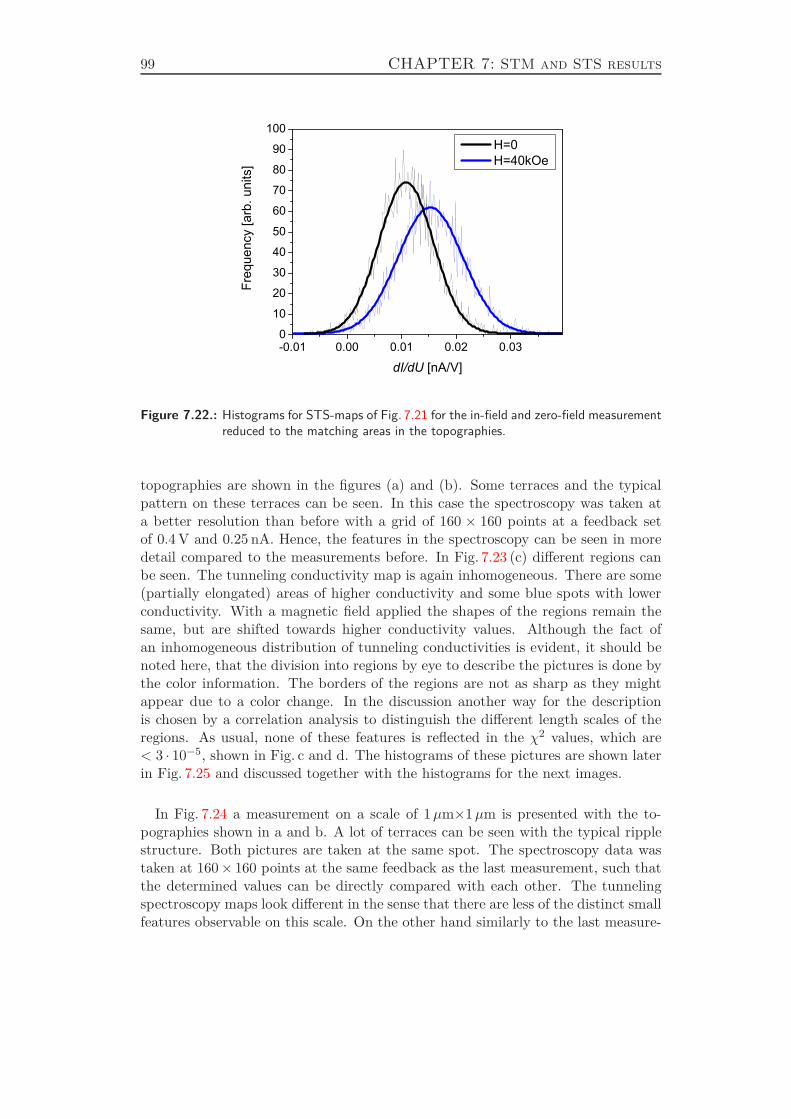
99 CHAPTER 7: STM and STS results
-0.01 0.00 0.01 0.02 0.030
10
20
30
40
50
60
70
80
90
100
Freq
uenc
y [a
rb. u
nits
]
dI/dU [nA/V]
H=0 H=40kOe
Figure 7.22.: Histograms for STS-maps of Fig. 7.21 for the in-field and zero-field measurementreduced to the matching areas in the topographies.
topographies are shown in the figures (a) and (b). Some terraces and the typicalpattern on these terraces can be seen. In this case the spectroscopy was taken ata better resolution than before with a grid of 160 × 160 points at a feedback setof 0.4 V and 0.25 nA. Hence, the features in the spectroscopy can be seen in moredetail compared to the measurements before. In Fig. 7.23 (c) different regions canbe seen. The tunneling conductivity map is again inhomogeneous. There are some(partially elongated) areas of higher conductivity and some blue spots with lowerconductivity. With a magnetic field applied the shapes of the regions remain thesame, but are shifted towards higher conductivity values. Although the fact ofan inhomogeneous distribution of tunneling conductivities is evident, it should benoted here, that the division into regions by eye to describe the pictures is done bythe color information. The borders of the regions are not as sharp as they mightappear due to a color change. In the discussion another way for the descriptionis chosen by a correlation analysis to distinguish the different length scales of theregions. As usual, none of these features is reflected in the χ2 values, which are< 3 · 10−5, shown in Fig. c and d. The histograms of these pictures are shown laterin Fig. 7.25 and discussed together with the histograms for the next images.
In Fig. 7.24 a measurement on a scale of 1µm×1µm is presented with the to-pographies shown in a and b. A lot of terraces can be seen with the typical ripplestructure. Both pictures are taken at the same spot. The spectroscopy data wastaken at 160× 160 points at the same feedback as the last measurement, such thatthe determined values can be directly compared with each other. The tunnelingspectroscopy maps look different in the sense that there are less of the distinct smallfeatures observable on this scale. On the other hand similarly to the last measure-
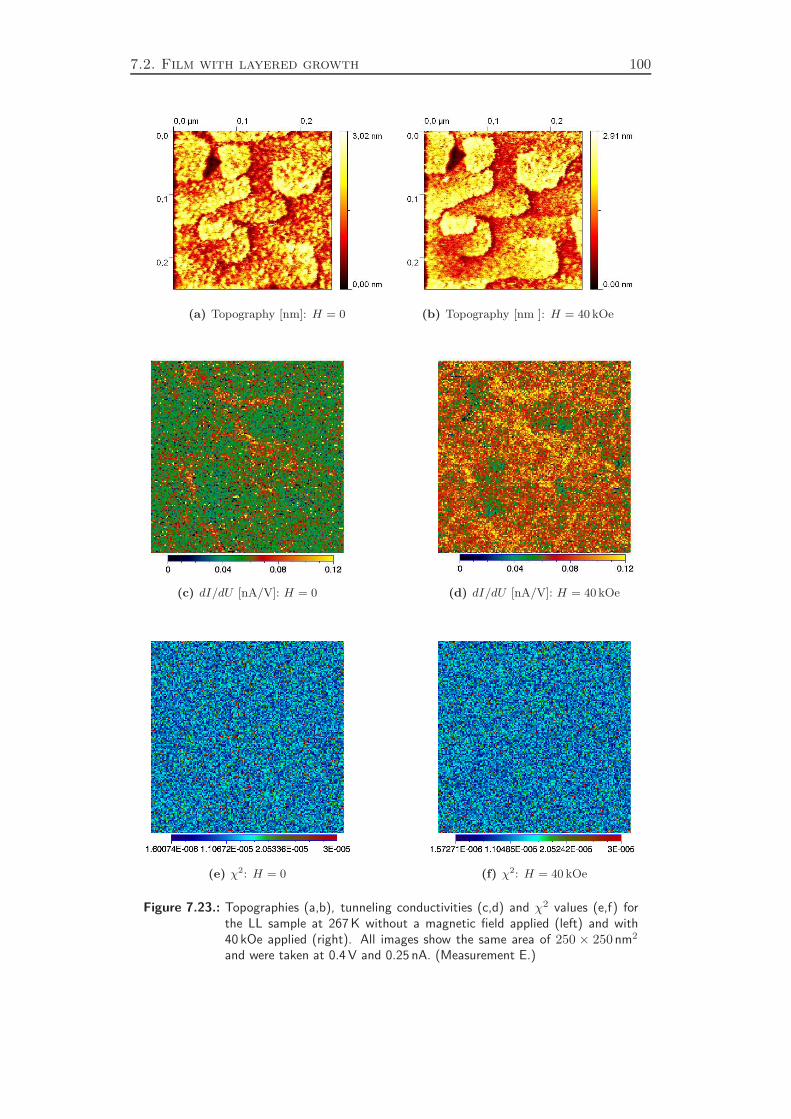
7.2. Film with layered growth 100
(a) Topography [nm]: H = 0 (b) Topography [nm ]: H = 40 kOe
(c) dI/dU [nA/V]: H = 0 (d) dI/dU [nA/V]: H = 40 kOe
(e) χ2: H = 0 (f) χ2: H = 40 kOe
Figure 7.23.: Topographies (a,b), tunneling conductivities (c,d) and χ2 values (e,f) forthe LL sample at 267 K without a magnetic field applied (left) and with40 kOe applied (right). All images show the same area of 250 × 250 nm2
and were taken at 0.4 V and 0.25 nA. (Measurement E.)
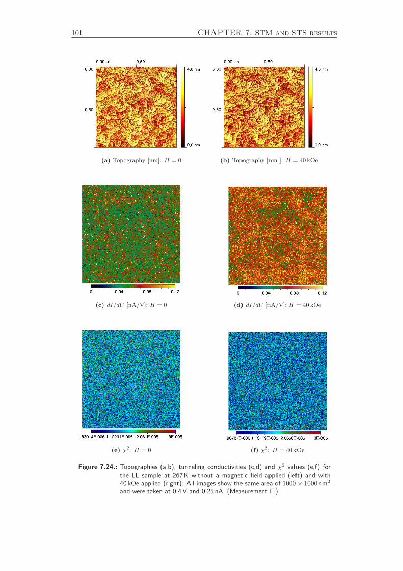
101 CHAPTER 7: STM and STS results
(a) Topography [nm]: H = 0 (b) Topography [nm ]: H = 40 kOe
(c) dI/dU [nA/V]: H = 0 (d) dI/dU [nA/V]: H = 40 kOe
(e) χ2: H = 0 (f) χ2: H = 40 kOe
Figure 7.24.: Topographies (a,b), tunneling conductivities (c,d) and χ2 values (e,f) forthe LL sample at 267 K without a magnetic field applied (left) and with40 kOe applied (right). All images show the same area of 1000× 1000 nm2
and were taken at 0.4 V and 0.25 nA. (Measurement F.)
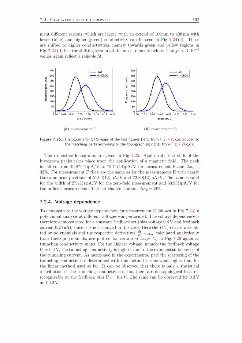
7.2. Film with layered growth 102
ment different regions, which are larger, with an extend of 100 nm to 400 nm withlower (blue) and higher (green) conductivity can be seen in Fig. 7.24 (c). Theseare shifted to higher conductivities, namely towards green and yellow regions inFig. 7.24 (d) like the shifting seen in all the measurements before. The χ2 < 3 ·10−5
values again reflect a reliable fit.
0.00 0.02 0.04 0.06 0.08 0.10 0.12 0.140
50
100
150
200
250
300
350
400
Freq
uenc
y [a
rb. u
nits
]
dI/dU [nA/V]
H=0 H=40kOe
(a) measurement F
0.00 0.02 0.04 0.06 0.08 0.10 0.12 0.140
50
100
150
200
250
300
350
400
Freq
uenc
y [a
rb. u
nits
]
dI/dU [nA/V]
H=0 H=40kOe
(b) measurement E
Figure 7.25.: Histograms for STS-maps of the last figures (left: from Fig. 7.23 c,d,reduced tothe matching parts according to the topographies; right: from Fig. 7.24 c,d).
The respective histograms are given in Fig. 7.25. Again a distinct shift of thehistogram peaks takes place upon the application of a magnetic field. The peakis shifted from 49.87(11)pA/V to 73.11(14)pA/V for measurement E and ∆σp is32%. For measurement F they are the same as for the measurement E with nearlythe same peak positions of 51.96(12) pA/V and 72.89(13) pA/V. The same is validfor the width of 27.4(3) pA/V for the zero-field measurement and 33.9(3)pA/V forthe in-field measurement. The net change is about ∆σp =29%.
7.2.4. Voltage dependence
To demonstrate the voltage dependence, for measurement E (shown in Fig. 7.23) apolynomial analysis at different voltages was performed. The voltage dependence istherefore demonstrated for a constant feedback set (bias voltage 0.4 V and feedbackcurrent 0.25 nA), since it is not changed in this case. Here the I(U)-curves were fit-ted by polynomials and the respective derivatives dIdU |U=U0 , calculated analyticallyfrom these polynomials, are plotted for certain voltages U0 in Fig. 7.26 again astunneling conductivity maps. For the highest voltage, namely the feedback voltageU = 0.4 V, the tunneling conductivity is highest due to the exponential behavior ofthe tunneling current. As mentioned in the experimental part the scattering of thetunneling conductivities determined with this method is somewhat higher than forthe linear method used so far. It can be observed that there is only a statisticaldistribution of the tunneling conductivities, but there are no topological featuresrecognizable at the feedback bias U0 = 0.4 V. The same can be observed for 0.3 Vand 0.2 V.
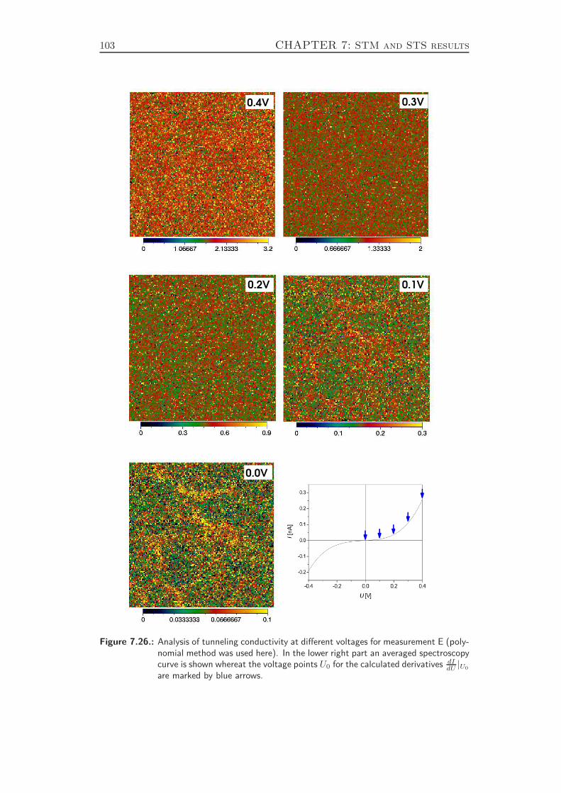
103 CHAPTER 7: STM and STS results
0.2V 0.1V
0.0V
0.4V 0.3V
Figure 7.26.: Analysis of tunneling conductivity at different voltages for measurement E (poly-nomial method was used here). In the lower right part an averaged spectroscopycurve is shown whereat the voltage points U0 for the calculated derivatives dI
dU|U0
are marked by blue arrows.
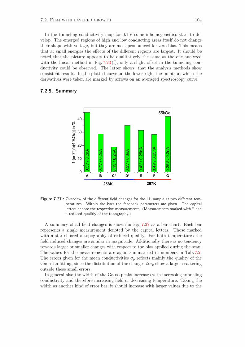
7.2. Film with layered growth 104
In the tunneling conductivity map for 0.1 V some inhomogeneities start to de-velop. The emerged regions of high and low conducting areas itself do not changetheir shape with voltage, but they are most pronounced for zero bias. This meansthat at small energies the effects of the different regions are largest. It should benoted that the picture appears to be qualitatively the same as the one analyzedwith the linear method in Fig. 7.23 (f), only a slight offset in the tunneling con-ductivity could be observed. The latter shows, that the analysis methods showconsistent results. In the plotted curve on the lower right the points at which thederivatives were taken are marked by arrows on an averaged spectroscopy curve.
7.2.5. Summary
A B C* D* E F G0
10
20
30
40
0.25
V /
0.2n
A
0.4V
/ 0.
25nA
0.5V
/ 0.
3nA
0.4V
/ 0.
25nA
0.4V
/ 0.
2nA
0.7V
/ 0.
2nA
258K
1-[σ
(0T)
/σ(4
0kO
e)] i
n %
267K
55kOe
0.5V
/ 0.
2nA
Figure 7.27.: Overview of the different field changes for the LL sample at two different tem-peratures. Within the bars the feedback parameters are given. The capitalletters denote the respective measurements. (Measurements marked with * hada reduced qualitiy of the topography.)
A summary of all field changes is shown in Fig. 7.27 as a bar chart. Each barrepresents a single measurement denoted by the capital letters. Those markedwith a star showed a topography of reduced quality. For both temperatures thefield induced changes are similar in magnitude. Additionally there is no tendencytowards larger or smaller changes with respect to the bias applied during the scan.The values for the measurements are again summarized in numbers in Tab. 7.2.The errors given for the mean conductivities σp reflects mainly the quality of theGaussian fitting, since the distribution of the changes ∆σp show a larger scatteringoutside these small errors.
In general also the width of the Gauss peaks increases with increasing tunnelingconductivity and therefore increasing field or decreasing temperature. Taking thewidth as another kind of error bar, it should increase with larger values due to the
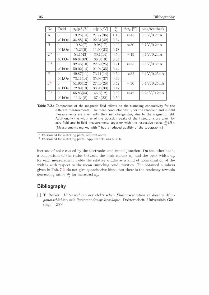
105 Bibliography
No. Field σp[pA/V] w[pA/V] wσp
∆σp [%] bias/feedback
A 0 19.26(14) 21.77(36) 1.13 ≈ 45 0.5 V/0.2 nA40 kOe 34.88(15) 22.31(42) 0.64
B 0 10.82(7) 9.98(17) 0.92 ≈ 30 0.7 V/0.2 nA40 kOe 15.26(9) 11.90(23) 0.78
C* 0 54.1(43) 30.1(14) 0.56 ≈ 19 0.4 V/0.2 nA40 kOe 66.84(63) 36.0(19) 0.54
D* 0 32.46(10) 22.50(25) 0.91 ≈ 35 0.5 V/0.3 nA40 kOe 50.02(14) 21.94(35) 0.44
E 0 49.87(11) 73.11(14) 0.54 ≈ 32 0.4 V/0.25 nA40 kOe 73.11(14) 35.93(37) 0.49
Fa 0 51.96(12) 27.40(28) 0.52 ≈ 30 0.4 V/0.25 nA40 kOe 72.89(13) 33.98(33) 0.47
Gb 0 65.83(53) 45.3(12) 0.69 ≈ 42 0.25 V/0.2 nA40 kOe 11.34(8) 67.4(22) 0.59
Table 7.2.: Comparison of the magnetic field effects on the tunneling conductivity for thedifferent measurements. The mean conductivities σp for the zero-field and in-fieldmeasurements are given with their net change ∆σp due to the magnetic field.Additionally the width w of the Gaussian peaks of the histograms are given forzero-field and in-field measurements together with the respective ratios w
σp(H).
(Measurements marked with * had a reduced qualitiy of the topography.)
aDetermined for matching parts, see text above.bDetermined for matching parts. Applied field was 55 kOe.
increase of noise caused by the electronics and tunnel junction. On the other hand,a comparison of the ratios between the peak centers σp and the peak width wpfor each measurement yields the relative widths as a kind of normalization of thewidths with respect to the mean tunneling conductivities. The obtained numbersgiven in Tab. 7.2, do not give quantitative hints, but there is the tendency towardsdecreasing ratios wσp for increased σp.
Bibliography
[1] T. Becker. Untersuchung der elektrischen Phasenseparation in dünnen Man-
ganatschichten mit Rastersondenspektroskopie. Doktorarbeit, Universität Göt-tingen, 2004.

Bibliography 106
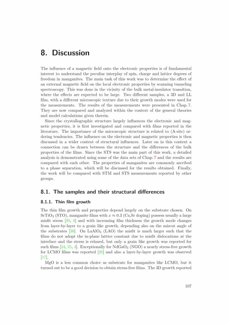
8. Discussion
The influence of a magnetic field onto the electronic properties is of fundamentalinterest to understand the peculiar interplay of spin, charge and lattice degrees offreedom in manganites. The main task of this work was to determine the effect ofan external magnetic field on the local electronic properties by scanning tunnelingspectroscopy. This was done in the vicinity of the bulk metal-insulator transition,where the effects are expected to be large. Two different samples, a 3D and LLfilm, with a different microscopic texture due to their growth modes were used forthe measurements. The results of the measurements were presented in Chap. 7.They are now compared and analyzed within the context of the general theoriesand model calculations given therein.
Since the crystallographic structure largely influences the electronic and mag-netic properties, it is first investigated and compared with films reported in theliterature. The importance of the microscopic structure is related to (A-site) or-dering tendencies. The influence on the electronic and magnetic properties is thendiscussed in a wider context of structural influences. Later on in this context aconnection can be drawn between the structure and the differences of the bulkproperties of the films. Since the STS was the main part of this work, a detailedanalysis is demonstrated using some of the data sets of Chap. 7 and the results arecompared with each other. The properties of manganites are commonly ascribedto a phase separation, which will be discussed for the results obtained. Finally,the work will be compared with STM and STS measurements reported by othergroups.
8.1. The samples and their structural differences
8.1.1. Thin film growth
The thin film growth and properties depend largely on the substrate chosen. OnSrTiO3 (STO), manganite films with x ≈ 0.3 (Ca,Sr doping) possess usually a largemisfit stress [28, 8] and with increasing film thickness the growth mode changesfrom layer-by-layer to a grain like growth, depending also on the miscut angle ofthe substrates [30]. On LaAlO3 (LAO) the misfit is much larger such that thefilms do not adopt the in-plane lattice constant due to misfit dislocations at theinterface and the stress is relaxed, but only a grain like growth was reported forsuch films [24, 25, 4]. Exceptionally for NdGaO3 (NGO) a nearly stress-free growthfor LCMO films was reported [28] and also a layer-by-layer growth was observed[17].
MgO is a less common choice as substrate for manganites like LCMO, but itturned out to be a good decision to obtain stress-free films. The 3D growth reported
107
8.1. The samples and their structural differences 108
for a large lattice mismatch, as mentioned above, cannot be generalized here andat least does not account for the MgO substrates, as demonstrated by the layer-by-layer (LL) growth. Here the films have practically the same thickness and theywere deposited on substrates of the same series, but they show a different micro-structure. The growth rate (see App. A) has obviously a large influence on thegrowth mode. In contrast to the LL sample, the 3D sample was deposited muchfaster, resulting in a three dimensional growth mode. It can be concluded that thediffusion times were much smaller and seemingly the growth did not correspond toa fully equilibrium condition.
It was already known from previous results that the films can be grown in a latticematched manner on MgO substrates. This was confirmed by in-plane texture X-ray measurements on the (220) reflex of LCMO [20]. As was shown in Fig. 6.5for the LL film, misfit dislocations occur in the La0.75Ca0.25MnO3 -film directlyat the interface to the substrate and therefore only 2-3 monolayers are epitaxiallystrained. Upon those the film growth is stress free, which is confirmed by the latticeparameters given in Tab. 6.1. The advantage of this kind of strain relaxation isthe exclusion of remaining stress in the films in contrast to totally strained films,grown on STO [8]. For a 3D film no HRTEM picture exists of the film - substrateinterface, but it can be expected that also for this film such dislocations exist,since the lattice parameter is very similar and the film does not appear to be fullystrained. On the other hand, some growth spirals within the grains can be seen,as indicated in Chap. 6.2, which means that a possible locally remaining strain dueto the larger deposition speed, is released by a somewhat different mechanism viascrew dislocations in growth spirals1.
Although the in-plane lattice parameters are very similar (Tab. 6.1), the filmsdeveloped a different crystal structure, namely the orthorhombic (Pnma) structure,typical of LCMO, is found for the 3D film and a pseudo-cubic or rhombohedral(R3c) structure is found for the LL film, as shown in Chap. 6.2, Fig. 6.6. This isa quite remarkable result, since normally only the lattice parameters change fordifferent substrates or deposition conditions, but generally the film structure re-tains the same geometry. The origin for this observation is given in the next section.
8.1.2. Ordering tendencies
In the theory (Chap. 2) it was already mentioned that ordering of the ions or orbitalsis expected to influence the properties of the manganites. From the discussion ofthe growth mode above, it can be concluded that not the macroscopic stress, whichis negligible here, but also the local ordering within the sample plays an importantrole. The reasons for this suspicion will be discussed in the following in terms ofthe structural ordering with respect to the properties of the samples. At first, theordering tendency is manifested by a particular LL film (called by LL-O in the
1A pure columnar growth, like it was observed in LSMO/MgO composite films on Al3O3 [10],was not observed in such a pronounced way in previous studies of LCMO on MgO [20]. (Thebehavior of the resistivity as a function of temperature would be different at low temperatures,if there were badly connected grains.)
109 CHAPTER 8: Discussion
following), which shows an A-site ordering (Fig. 8.1), that is, the La and Ca ionsare found on well defined lattice sites forming two sublattices [21]. Although sucha strict ordering was not seen for the LL film used for the STS measurements ofthis work, the tendency to a more ordered structure is evident by the morphologyand the crystal structure.
20 40 60 80 100250
260
270
280
290
300
x≈1/4
T MI (K
)
α max=MAX[(dR/R)/(dT/T)]
x≈0.3
(a) Comparison transition (b) A-site order
Figure 8.1.: (a): Transition temperature TMI versus sharpness of transition in comparisonwith different samples. The 3D and LL samples used here are marked by the redand green triangle, respectively. The LL-O film is represented by the point nearbyαmax = 100. (b): Schematic representation of A-site ordering in LL-O film in thea− b-plane as a projection along the [001]c direction.
Another indication for these ordering tendencies are the bulk electronic and mag-netic properties. In Chap. 2 the importance of the structure and lattice distortionsfor the electronic and magnetic properties were discussed in terms of the influenceof the Mn-O-Mn bonds and their bond angles on the exchange mechanisms. Fromthis point of view a change of the properties can be expected for these films withtheir different structural characteristics. It is indeed the case that the magneticand electronic transitions differ with respect to their parameters for both sam-ples (shown in Chap. 6): The transition temperature, that is TMI and TC , aresmaller for the 3D film, while for the LL film the values are the highest reportedfor La0.75Ca0.25MnO3 thin films. Additionally the sharpness of the transition αmax(see p. 71) has been mentioned in Chap. 6.3. It rises with the ordering tendency,which is demonstrated in Fig. 8.1, in which different films of the series were com-pared. The graph shows TMI as a function of αmax, whereat a second series ofLa1−xCaxMnO3 films with x = 0.3 is added. The latter shows the same tendencyas the La0.75Ca0.25MnO3 films. The 3D film used within this work is marked bya red and the LL by a green triangle, respectively. The A-site ordered LL-O filmcorresponds to the outermost point on the right nearby αmax ∼= 100. Remarkablythe sharpness of the transition increases with increasing TMI up to a certain value,where the transition temperatures seem to saturate. In other words here the TMI isgiven by the composition and its most ordered structure and can be shifted towards
8.1. The samples and their structural differences 110
lower temperatures by disorder, which also broadens the transition.The resistivity for the 3D sample is also higher than for the LL film, but only
below the MIT. Above the MIT the resistivities are nearly equal, which does notnecessarily contradict the results about ordering, since above TMI a thermallyactivated transport is expected and therefore the role of the structural ordering isless important, as the transport mechanism is different. The LL-O film fits intothis considerations, since its resistivity lies slightly below the one of the LL filmhere [21].
Evenly the ferro/paramagnetic transition fits into this picture. From the theories(Chap. 2) a direct coupling of the magnetic ordering to the electronic properties isindisputable. There are a lot of hints from experiments, which underline thesemodels (although it never could be proved by a direct measurement). The temper-ature of the magnetic transition was shown in Fig. 6.8 and the critical temperatureTC is about the same for the LL film and the 3D film, but the sharpness of thetransition is broader for the 3D film, like the sharpness of the MIT.
All these differences in the sample properties due to the structural characteristicsare an indication for a different degree of A-site ordering. The first peculiarity isthe saturation of TMI at a value of about 270 K. This seems to be the maximum,which can be reached for the given doping, x = 0.25, and can be associated with the“ideal” case for La0.75Ca0.25MnO3 . Ideal means that the structural ordering leadsto a perfect arrangement of Mn-O-Mn bonds, such that the electronic propertiesare optimized. The A-site ordering in the LL-O films additionally supports an idealregular pattern within the sample with its superstructure and four times larger unitcell.
The orthorhombic structure breaks the cubic symmetry, which changes the Mn-Obond angles slightly compared to the cubic structure. An absolute equivalence ofthe Mn-O bonds is no more possible. The 3D sample shows a different morphologyand it cannot be excluded that locally the sample is strained, although the macro-scopic lattice parameter does not support a strained sample. For LCMO/STO filmsit was for example found that the centers of the islands are unstrained, while theedges are strained regions [4]. Local strain effects (extending over a few latticesites) would not be expected under a A-site ordering, since the ions with slightlydifferent radii (Chap. 2.3) are distributed in a regular pattern. But for a randomdistribution of the A-site ions different distortions of the local lattice are expected.In other words, the electronic properties, expressed by the mobility of the chargecarriers, are coupled to the structure and therefore are determined by the latter,as demonstrated here.
Another issue, which provides further evidence for a scaling of the sharpnessof the transition with the microscopic order within the films, is the structuraltransition observed by Radaelli [23], compare Chap. 2.3. The group examined thechange of the Mn-O bond lengths and angles together with the Jahn-Teller dis-tortions. Consequently there must be a connection with the structures observedand the shifted and broadened MIT of the 3D films. For a quantitative discussionhighly resolved temperature dependent neutron scattering experiments would benecessary, but here some qualitative arguments can be highlighted.
The ordering, structure and sharpness of the transition seem to be related to
111 CHAPTER 8: Discussion
each other and two attempts of an explanation will be given now. In the rhom-bohedral structure, which here is associated with a higher chemical ordering, allMn-O bond lengths are the same, since octahedral distortions are missing. Acrossthe transition, the changes of the bond angles might cost less effort if the structureis more symmetric, which in this sense is the case for the rhombohedral structure,all Mn-O-Mn bond angles and lengths are equal, compared to the orthorhombicstructure (see structural description on p. 9 and Fig. 2.4). Therefore the transi-tion can take place within a smaller temperature region and appears to be muchsharper. Due to the remaining Jahn-Teller distortions in the orthorhombic 3D filmsthe structural rearrangement is more complicated and restricted. The mean bondlengths and angles could then be expected to remain larger (smaller) than for theother phase. Therefore the bandwidth, which is dependent on these bond lengths(angles), would remain smaller in accordance to a higher resistivity. The LL-O filmwith its commensurate superstructure would also fit into this picture. Due to theordering the undisturbed system is expected to change in a cooperative manner(probably slightly comparable to a martensitic transition).
Another possibility is a distribution of different local strain fields and/or localcompositions coming along with the disorder. It is known that strain, caused hereby disorder on a microscopic scale, can lead to a decrease in the transition temper-ature, and therefore locally different transition temperatures can occur. Then thedifferent regions within the film undergo the MIT at slightly different temperaturesand the transition appears to be broadened compared to an ideally ordered sam-ple. Concurrently the mean transition temperature also can be reduced. Again thebandwidth would be reduced for the disordered cases, since the bond lengths andoctahedral distortions, which are caused by the disorder and a random distributionof ionic radii, remain in the sample.
8.2. Spectroscopy
8.2.1. Magnetic effects on the local tunneling conductance
In Chap. 7 the main results were shown for the 3D and LL samples. The I(U)curves were analyzed using the fitting procedures in Sec. 5.3 and Fig. 5.12. Now,the spectroscopy curves will be analyzed and discussed in detail with respect to theregions of different tunneling conductivity and the influence of a magnetic field.The 3D and LL sample will be compared with each other, but the emphasis liesmore on the LL measurements.
It should be mentioned that for magnetic fields of 40 kOe the sample magnetiza-tion is expected to be saturated as confirmed by the hysteresis curves taken nearthe metal-insulator transition displayed in Fig. 6.8. Although there is no saturationreached for the MR in the lower panel of Fig. 6.9, most of the changes due to amagnetic field are already reached at 40 kOe as can be seen by the much smallerslope for that region compared to the steep decrease for fields ≤ 20 kOe. Maybe dueto the small energies of magnetic fields a real saturation in resistivity might neverbe reached. This is a general observation for manganites. In addition for 40 kOealso the magnetization at the surface is expected to be at least close to saturation
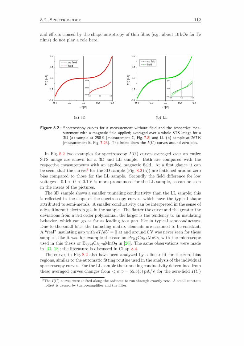
8.2. Spectroscopy 112
and effects caused by the shape anisotropy of thin films (e.g. about 10 kOe for Fefilms) do not play a role here.
-0.4 -0.2 0.0 0.2 0.4-0.2
-0.1
0.0
0.1
0.2
-0.1 0.0 0.1-0.005
0.000
0.005
I(U) [
nA]
U [V]
no field field
(a) 3D
-0.4 -0.2 0.0 0.2 0.4-0.2
-0.1
0.0
0.1
0.2
-0.1 0.0 0.1-0.01
0.00
0.01
I(U) [
nA]
U [V]
no field field
(b) LL
Figure 8.2.: Spectroscopy curves for a measurement without field and the respective mea-surement with a magnetic field applied; averaged over a whole STS image for a3D (a) sample at 258 K [measurement C, Fig. 7.8] and LL (b) sample at 267 K[measurement E, Fig. 7.23]. The insets show the I(U) curves around zero bias.
In Fig. 8.2 two examples for spectroscopy I(U) curves averaged over an entireSTS image are shown for a 3D and LL sample. Both are compared with therespective measurements with an applied magnetic field. At a first glance it canbe seen, that the curves2 for the 3D sample (Fig. 8.2 (a)) are flattened around zerobias compared to those for the LL sample. Secondly the field difference for lowvoltages −0.1 < U < 0.1 V is more pronounced for the LL sample, as can be seenin the insets of the pictures.
The 3D sample shows a smaller tunneling conductivity than the LL sample; thisis reflected in the slope of the spectroscopy curves, which have the typical shapeattributed to semi-metals. A smaller conductivity can be interpreted in the sense ofa less itinerant electron gas in the sample. The flatter the curve and the greater thedeviations from a 3rd order polynomial, the larger is the tendency to an insulatingbehavior, which can go as far as leading to a gap, like in typical semiconductors.Due to the small bias, the tunneling matrix elements are assumed to be constant.A “real” insulating gap with dI/dU = 0 at and around 0 V was never seen for thesesamples, like it was for example the case on Pr0.7Ca0.3MnO3 with the microscopeused in this thesis or Bi0.24Ca0.76MnO3 in [26]. The same observations were madein [33, 18]; the literature is discussed in Chap. 8.4.
The curves in Fig. 8.2 also have been analyzed by a linear fit for the zero biasregions, similar to the automatic fitting routine used in the analysis of the individualspectroscopy curves. For the LL sample the tunneling conductivity determined fromthese averaged curves changes from < σ >= 55.5(5) pA/V for the zero-field I(U)
2The I(U) curves were shifted along the ordinate to run through exactly zero. A small constantoffset is caused by the preamplifier and the filter.
113 CHAPTER 8: Discussion
curve to< σ(40 kOe) >= 79.1(5) pA/V for the field curve, while for the 3D sample amuch smaller change from < σ >= 24.2(2) pA/V to < σ(40 kOe) >= 26.9(2) pA/Vcan be determined. The values for the LL sample are similar to those obtainedfrom the histogram peak positions (see Tab.7.2, p. 105) within the statistical errorof the linear regression. This underlines the quality and consistency of the computerbased analysis of the measurements. Those from the 3D sample are also similar tothe histogram peak positions in Tab.7.1, p. 90, but a little bit larger. A clear rise ofthe slope for the in-field measurement of the LL sample can be seen (∆σ ≈ 30 %),but the effect is considerably smaller for the 3D sample (∆σ ≈ 10 %). It shouldbe repeated that the rise of the tunneling conductivity of the 3D sample due toan external magnetic field is quite small (compare Tab. 7.1) compared to the widthof the histogram peaks shown in the last chapter (e.g. Fig. 7.10). The absoluteshift σp(H) − σp(0) = 3.33 pA/V for the 3D sample (measurement C, p. 87)compared to the width of the histogram for zero field w(0) = 10.45 pA/V is verysmall [σp(H) − σp(0)]/w(0) ≃ 0.32. Therefore differences for the spectroscopycurves caused by the magnetic field are hardly visible, although the bulk MR is aslarge as for the LL sample as shown in Fig. 6.9. In the case of the LL sample achange of the slope around zero bias can be already seen in the inset of Fig. 8.2 (b).Here the absolute shift σp(H) − σp(0) = 23.24 pA/V (measurement E, p. 102)compared to the width of the histogram for zero field w(0) = 27.35 pA/V is muchmore pronounced [σp(H) − σp(0)]/w(0) ≃ 0.85. The same observations apply forthe other measurements of the 3D and the LL sample, not shown.
Compared to the width of the distribution of the tunneling conductivities thechanges in tunneling conductivity caused by the magnetic field are much morepronounced for the LL film than for the 3D film. In other words, the shift of thetunneling conductivity with an applied magnetic field are much better resolved foran LL film than for a 3D film.
In the following the local spectroscopy is analyzed in more detail with respectto the different regions of tunneling conductivity for the LL film. In Fig. 8.3 fourdifferent spectroscopy curves are compared with each other. The spectroscopy dataof parts with lower (black and blue curves) and higher (red and orange curves)tunneling conductivity were averaged over the regions marked by the black andwhite boxes in Fig. 8.3 (a,b), respectively. The same regions were selected fromMeasurement E without a field applied (black and red) and with a field applied(blue and orange). From the I(U)-curves the differences in tunneling conductivitycan be seen for higher and lower conducting regions. The black and blue curveshave both smaller tunneling conductivities than the red and orange curves. Withthe application of a magnetic field, both conductivities are shifted by nearly thesame value.3 (This is consistent with the fact, that the histograms (Fig. 7.25 (a),p. 102) for the measurements with and without field overlap.) This can be seen even
3The small effects might be caused by some contaminations on the surface due to the ex-situpreparation, but this is not very likely. Some hints of carbon were found in an XPS measure-ment and in [32], but the authors talk about less than a monolayer. If a surface preparationwould help is not clear, one try by sputtering and heating in air with an LL film of a newerseries did not result in reliable measurements. There are recent temperature dependent STSmeasurements from another group, which confirm these measurements [18].
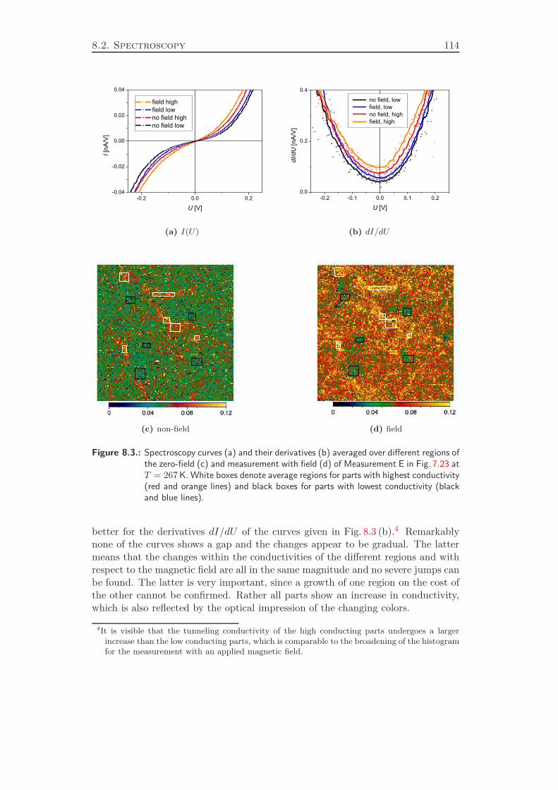
8.2. Spectroscopy 114
-0.2 0.0 0.2-0.04
-0.02
0.00
0.02
0.04
I [nA
/V]
U [V]
field high field low no field high no field low
(a) I(U)
-0.2 -0.1 0.0 0.1 0.20.0
0.2
0.4
dI/dU
[nA
/V]
U [V]
no field, low field, low no field, high field, high
(b) dI/dU
(c) non-field (d) field
Figure 8.3.: Spectroscopy curves (a) and their derivatives (b) averaged over different regions ofthe zero-field (c) and measurement with field (d) of Measurement E in Fig. 7.23 atT = 267 K. White boxes denote average regions for parts with highest conductivity(red and orange lines) and black boxes for parts with lowest conductivity (blackand blue lines).
better for the derivatives dI/dU of the curves given in Fig. 8.3 (b).4 Remarkablynone of the curves shows a gap and the changes appear to be gradual. The lattermeans that the changes within the conductivities of the different regions and withrespect to the magnetic field are all in the same magnitude and no severe jumps canbe found. The latter is very important, since a growth of one region on the cost ofthe other cannot be confirmed. Rather all parts show an increase in conductivity,which is also reflected by the optical impression of the changing colors.
4It is visible that the tunneling conductivity of the high conducting parts undergoes a largerincrease than the low conducting parts, which is comparable to the broadening of the histogramfor the measurement with an applied magnetic field.
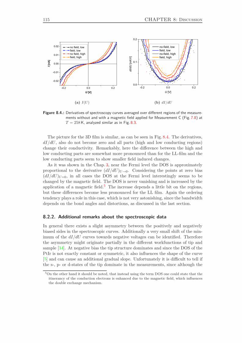
115 CHAPTER 8: Discussion
-0.2 0.0 0.2
-0.02
-0.01
0.00
0.01
0.02I [
nA]
U [V]
no field, low field, low no field, high field, high
(a) I(U)
-0.2 0.0 0.20.0
0.1
0.2
dI/d
U [n
A/V
]
U [V]
no-field, low field, low no-field, high field, high
(b) dI/dU
Figure 8.4.: Derivatives of spectroscopy curves averaged over different regions of the measure-ments without and with a magnetic field applied for Measurement C (Fig. 7.8) atT = 258 K, analyzed similar as in Fig. 8.3.
The picture for the 3D film is similar, as can be seen in Fig. 8.4. The derivatives,dI/dU , also do not become zero and all parts (high and low conducting regions)change their conductivity. Remarkably, here the difference between the high andlow conducting parts are somewhat more pronounced than for the LL-film and thelow conducting parts seem to show smaller field induced changes.
As it was shown in the Chap. 3, near the Fermi level the DOS is approximatelyproportional to the derivative (dI/dU)U→0. Considering the points at zero bias(dI/dU)U=0, in all cases the DOS at the Fermi level interestingly seems to bechanged by the magnetic field. The DOS is never vanishing and is increased by theapplication of a magnetic field.5 The increase depends a little bit on the regions,but these differences become less pronounced for the LL film. Again the orderingtendency plays a role in this case, which is not very astonishing, since the bandwidthdepends on the bond angles and distortions, as discussed in the last section.
8.2.2. Additional remarks about the spectroscopic data
In general there exists a slight asymmetry between the positively and negativelybiased sides in the spectroscopic curves. Additionally a very small shift of the min-imum of the dI/dU curves towards negative voltages can be identified. Thereforethe asymmetry might originate partially in the different workfunctions of tip andsample [34]. At negative bias the tip structure dominates and since the DOS of thePtIr is not exactly constant or symmetric, it also influences the shape of the curve[5] and can cause an additional gradual slope. Unfortunately it is difficult to tell ifthe s-, p- or d-states of the tip dominate in the measurements, since although the
5On the other hand it should be noted, that instead using the term DOS one could state that theitinerancy of the conduction electrons is enhanced due to the magnetic field, which influencesthe double exchange mechanism.
8.3. Phase separation 116
states from the d-orbitals should contribute most (and are most asymmetric), theirdecay is very sharp [11]. Also it is difficult to distinguish between the tip statesand sample states in this case, as no distinct structures can be found in the dI/dUcurves. An asymmetry in otherwise unstructured curves has also been observed byfor instance Mitra et al. [17] on similar samples, who ascribe the asymmetry tosomewhat different distributions of DOS for filled and unfilled states, which is an-other possibility. Charging effects or large space charge regions are not very likelyin this case and would rather be expected on the highly insulating manganites.
Pickett et al. have performed a calculation of the DOS for La0.75Ca0.25MnO3 [22],which does not show any distinct structures at ±0.5 eV with respect to the Fermiedge. The same result is confirmed by a photoemission spectroscopy measurement[15].6 But interestingly Pickett et al. used also a superstructure for their calculationand proposed a dependence of the DOS, particularly for the minority states, on thedisorder. Unfortunately no predictions concerning the temperature evolution ormagnetic field induced changes of the DOS have been made.
8.3. Phase separation
The term phase separation means the existence and interplay of two competingphases in the vicinity of a first order phase transition. Several computing modelsof the metal-insulator transition in manganites are based on phase separation toexplain the CMR effect and are confirmed by some experiments. The two com-peting phases are mostly ascribed to a ferromagnetic metallic and antiferromag-netic/charge ordered insulating phase. The universality of phase separation forall manganite compounds is still under debate, since most of the models consideronly small band width manganites, like (La1−yPry)5/8Ca3/8MnO3 (LPCMO), whichshow a charge-ordered state at low temperatures.
In the last section the effects of magnetic fields on the tunneling spectroscopycurves were discussed in detail by means of some examples. At first it was shownthat there are gradual changes in the tunneling conductivity over the surface areasexamined. Secondly, for an applied magnetic field the tunneling conductivity forall of the regions is shifted to a higher value. Third, there is no growth of onekind of regions on the cost of others, that is no nucleation behavior was observed.That there is no sharp boundary between the different regions, in contrast to atom-ically sharp phase boundaries reported by Renner et al. [26], is another importantobservation.
Both 3D and LL films show a similar behavior in their electronic and magneticproperties and seem to follow the same mechanism, although some differences,especially in the range of the length scales according to lattice effects, were outlined.Another film, the LL-O film with A-site ordering, showed no phase separation[21, 33] and has the sharpest metal-insulator transition with the highest TMI .Another work7 provides some hints about the same mechanisms with respect to
6For a direct comparison, a deconvolution of the sample and tip DOS and the transmissioncoefficients is necessary, which is not trivial.
7Diploma work in progress, Thomas Mildner.
117 CHAPTER 8: Discussion
magnetic fields for the A-site ordered LL-O film. Namely the tunneling conductivityalso seems to change all over the scanned area.
In this section the sample properties will be considered in the context of phaseseparation and different related theories (see Chap. 2.2). The (locally pinned) re-gions with different conductivities might be called phases.8 These phases cannotbe identified here on the atomic scale, like it was done by Renner et al. [26]. Thisthesis concentrates on a scale of about 2 – 1000 nm.9 Below these length scale nodirect measurements could be done with the existing setup and no predictions canbe made about phase arrangements on a scale close to atomic resolution.
8.3.1. Is there a distinct two phase behavior?
The histograms of the LL samples show a symmetric (Gaussian) distribution, whichdoes not imply any multiphase coexistence. In contrast, the histograms for the 3Dsample are somewhat asymmetric. One therefore could assume two Gaussian com-ponents as demonstrated in Fig. 8.5. In the figures (a) and (b) the same histogramsfor a measurement at zero field are shown. There are two different possibilities offitting the data. At a first glance, the sum of the Gaussian peaks shown in redin graph (a) is a good fit of the data. The peaks of both components are locatedat centers of σp1 = 13.6(7) pA/V and σp2 = 25(6) pA/V. In graph (b) the datais less well fitted with σp1 = 16.8(8) pA/V and σp2 = 37(7) pA/V. Additionallythe data of the measurement within a magnetic field, given by the subfigure (c)was also analyzed this way. Here the peak centers are σp1 = 18.5(6) pA/V andσp2 = 31(9) pA/V.
If now the figures (a) and (c) are compared with each other, both peak centersare shifted to higher conductivities, which is consistent with the results discussed sofar. The component of high tunneling conductivity becomes smaller in height – andalso the area under the peak is decreased. This observation contradicts a model inwhich the proportion of high conducting parts increases with the application of amagnetic field. The situation shown in (b) would be even less physically probable,since the peak center for the high conductivity is decreased for the histogram ofthe measurement in a magnetic field. This analysis together with the analysis ofthe other measurements did not lead to a well-defined result.
The change over from one phase (region) to the other is demonstrated in Fig. 8.6.Here the data of Measurement E of the 3D film were taken, due to the higherresolution of the spectroscopy grid. Individual spectroscopy curves along a line areshown between a low and high conducting part. The transition is continuous orotherwise two bundles of curves would be expected. If there was an atomicallysharp boundary extended over several nanometers between two phases, as seen byRenner et al. [26] on a very small part of the sample, it also would show up as
8The term "phase" here does not necessarily mean a phase in a classical thermodynamic descrip-tion. The lack of a clear definition of the phases in manganites implies the risk of disaccordsin the discussion about phases.
9The resolution given here does not mean, that with one spectroscopy point a region with diam-eter of 2 nm is covered, the latter is much smaller, but a definition of a region which is coveredby the tunneling current is quite difficult and should not be discussed here. The resolutionhere is already limited by the number of spectroscopy points per area.
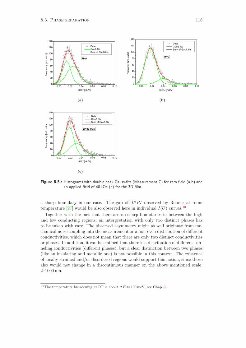
8.3. Phase separation 118
0.00 0.02 0.04 0.06 0.08 0.100
20
40
60
80
100
120
140
H=0
Data Gauß fits Sum of Gauß fits
dI/dU [nA/V]
Freq
uenc
y [a
rb. u
nits
]
(a)
0.00 0.02 0.04 0.06 0.08 0.100
20
40
60
80
100
120
140
H=0
Data Gauß fits Sum of Gauß fits
dI/dU [nA/V]
Freq
uenc
y [a
rb. u
nits
]
(b)
0.00 0.02 0.04 0.06 0.08 0.100
20
40
60
80
100
120
140 Data Gauß fits Sum of Gauß fits
H=40 kOe
dI/dU [nA/V]
Freq
uane
cy [a
rb. u
nits
]
(c)
Figure 8.5.: Histograms with double peak Gauss-fits (Measurement C) for zero field (a,b) andan applied field of 40 kOe (c) for the 3D film.
a sharp boundary in our case. The gap of 0.7 eV observed by Renner at roomtemperature [27] would be also observed here in individual I(U) curves.10
Together with the fact that there are no sharp boundaries in between the highand low conducting regions, an interpretation with only two distinct phases hasto be taken with care. The observed asymmetry might as well originate from me-chanical noise coupling into the measurement or a non-even distribution of differentconductivities, which does not mean that there are only two distinct conductivitiesor phases. In addition, it can be claimed that there is a distribution of different tun-neling conductivities (different phases), but a clear distinction between two phases(like an insulating and metallic one) is not possible in this context. The existenceof locally strained and/or disordered regions would support this notion, since thosealso would not change in a discontinuous manner on the above mentioned scale,2–1000 nm.
10The temperature broadening at RT is about ∆E ≈ 100 meV, see Chap. 3.
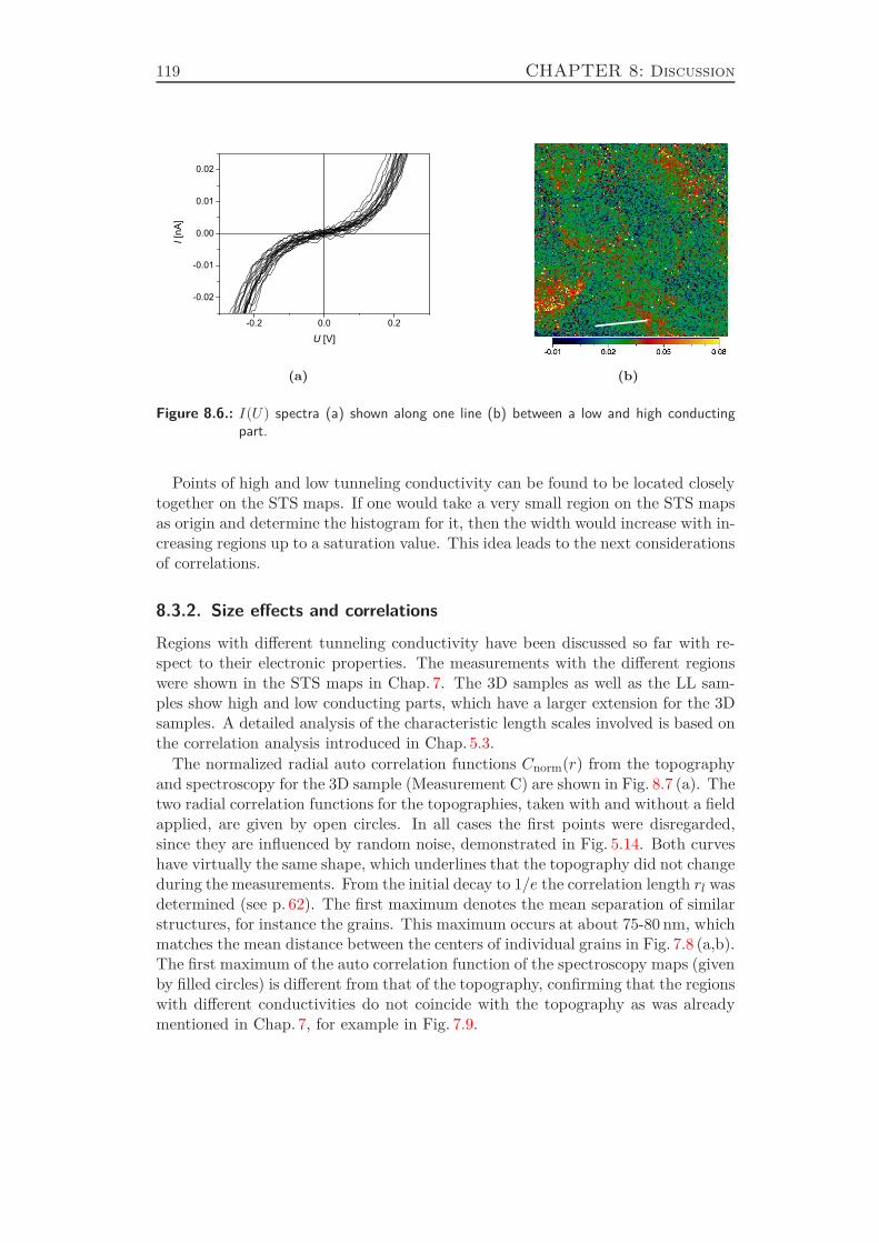
119 CHAPTER 8: Discussion
-0.2 0.0 0.2
-0.02
-0.01
0.00
0.01
0.02I [nA
]
U [V]
(a) (b)
Figure 8.6.: I(U) spectra (a) shown along one line (b) between a low and high conductingpart.
Points of high and low tunneling conductivity can be found to be located closelytogether on the STS maps. If one would take a very small region on the STS mapsas origin and determine the histogram for it, then the width would increase with in-creasing regions up to a saturation value. This idea leads to the next considerationsof correlations.
8.3.2. Size effects and correlations
Regions with different tunneling conductivity have been discussed so far with re-spect to their electronic properties. The measurements with the different regionswere shown in the STS maps in Chap. 7. The 3D samples as well as the LL sam-ples show high and low conducting parts, which have a larger extension for the 3Dsamples. A detailed analysis of the characteristic length scales involved is based onthe correlation analysis introduced in Chap. 5.3.
The normalized radial auto correlation functions Cnorm(r) from the topographyand spectroscopy for the 3D sample (Measurement C) are shown in Fig. 8.7 (a). Thetwo radial correlation functions for the topographies, taken with and without a fieldapplied, are given by open circles. In all cases the first points were disregarded,since they are influenced by random noise, demonstrated in Fig. 5.14. Both curveshave virtually the same shape, which underlines that the topography did not changeduring the measurements. From the initial decay to 1/e the correlation length rl wasdetermined (see p. 62). The first maximum denotes the mean separation of similarstructures, for instance the grains. This maximum occurs at about 75-80 nm, whichmatches the mean distance between the centers of individual grains in Fig. 7.8 (a,b).The first maximum of the auto correlation function of the spectroscopy maps (givenby filled circles) is different from that of the topography, confirming that the regionswith different conductivities do not coincide with the topography as was alreadymentioned in Chap. 7, for example in Fig. 7.9.
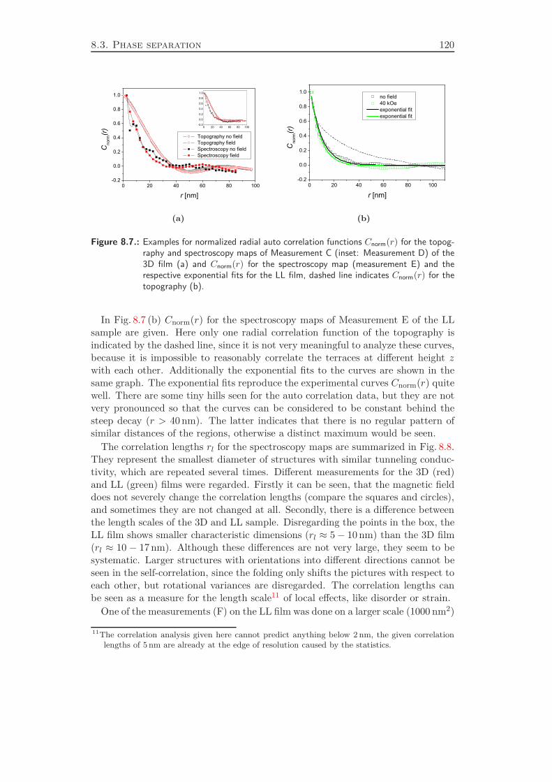
8.3. Phase separation 120
0 20 40 60 80 100-0.2
0.0
0.2
0.4
0.6
0.8
1.0
0 20 40 60 80 100-0.2
0.0
0.2
0.4
0.6
0.8
1.0
Cno
rm(r)
r [nm]
Topography no field Topography field Spectroscopy no field Spectroscopy field
(a)
0 20 40 60 80 100-0.2
0.0
0.2
0.4
0.6
0.8
1.0
Cno
rm(r)
r [nm]
no field 40 kOe exponential fit exponential fit
(b)
Figure 8.7.: Examples for normalized radial auto correlation functions Cnorm(r) for the topog-raphy and spectroscopy maps of Measurement C (inset: Measurement D) of the3D film (a) and Cnorm(r) for the spectroscopy map (measurement E) and therespective exponential fits for the LL film, dashed line indicates Cnorm(r) for thetopography (b).
In Fig. 8.7 (b) Cnorm(r) for the spectroscopy maps of Measurement E of the LLsample are given. Here only one radial correlation function of the topography isindicated by the dashed line, since it is not very meaningful to analyze these curves,because it is impossible to reasonably correlate the terraces at different height zwith each other. Additionally the exponential fits to the curves are shown in thesame graph. The exponential fits reproduce the experimental curves Cnorm(r) quitewell. There are some tiny hills seen for the auto correlation data, but they are notvery pronounced so that the curves can be considered to be constant behind thesteep decay (r > 40 nm). The latter indicates that there is no regular pattern ofsimilar distances of the regions, otherwise a distinct maximum would be seen.
The correlation lengths rl for the spectroscopy maps are summarized in Fig. 8.8.They represent the smallest diameter of structures with similar tunneling conduc-tivity, which are repeated several times. Different measurements for the 3D (red)and LL (green) films were regarded. Firstly it can be seen, that the magnetic fielddoes not severely change the correlation lengths (compare the squares and circles),and sometimes they are not changed at all. Secondly, there is a difference betweenthe length scales of the 3D and LL sample. Disregarding the points in the box, theLL film shows smaller characteristic dimensions (rl ≈ 5− 10 nm) than the 3D film(rl ≈ 10 − 17 nm). Although these differences are not very large, they seem to besystematic. Larger structures with orientations into different directions cannot beseen in the self-correlation, since the folding only shifts the pictures with respect toeach other, but rotational variances are disregarded. The correlation lengths canbe seen as a measure for the length scale11 of local effects, like disorder or strain.
One of the measurements (F) on the LL film was done on a larger scale (1000 nm2)
11The correlation analysis given here cannot predict anything below 2 nm, the given correlationlengths of 5 nm are already at the edge of resolution caused by the statistics.
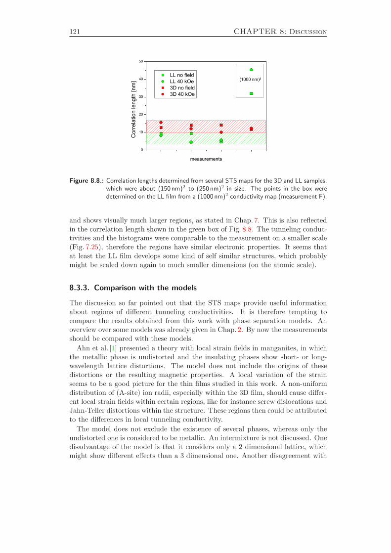
121 CHAPTER 8: Discussion
0
10
20
30
40
50
Cor
rela
tion
leng
th [n
m]
measurements
LL no field LL 40 kOe 3D no field 3D 40 kOe
(1000 nm)²
Figure 8.8.: Correlation lengths determined from several STS maps for the 3D and LL samples,which were about (150 nm)2 to (250 nm)2 in size. The points in the box weredetermined on the LL film from a (1000 nm)2 conductivity map (measurement F).
and shows visually much larger regions, as stated in Chap. 7. This is also reflectedin the correlation length shown in the green box of Fig. 8.8. The tunneling conduc-tivities and the histograms were comparable to the measurement on a smaller scale(Fig. 7.25), therefore the regions have similar electronic properties. It seems thatat least the LL film develops some kind of self similar structures, which probablymight be scaled down again to much smaller dimensions (on the atomic scale).
8.3.3. Comparison with the models
The discussion so far pointed out that the STS maps provide useful informationabout regions of different tunneling conductivities. It is therefore tempting tocompare the results obtained from this work with phase separation models. Anoverview over some models was already given in Chap. 2. By now the measurementsshould be compared with these models.
Ahn et al. [1] presented a theory with local strain fields in manganites, in whichthe metallic phase is undistorted and the insulating phases show short- or long-wavelength lattice distortions. The model does not include the origins of thesedistortions or the resulting magnetic properties. A local variation of the strainseems to be a good picture for the thin films studied in this work. A non-uniformdistribution of (A-site) ion radii, especially within the 3D film, should cause differ-ent local strain fields within certain regions, like for instance screw dislocations andJahn-Teller distortions within the structure. These regions then could be attributedto the differences in local tunneling conductivity.
The model does not exclude the existence of several phases, whereas only theundistorted one is considered to be metallic. An intermixture is not discussed. Onedisadvantage of the model is that it considers only a 2 dimensional lattice, whichmight show different effects than a 3 dimensional one. Another disagreement with
8.3. Phase separation 122
the results of this work is the prediction about the effects of magnetic fields. Thelatter should increase the metallic volume fraction according to the model, which isnot the case here. Unfortunately small local rearrangements of the distortions of allregions to veer toward a less distorted case within a structural transition coupledto the metal-insulator transition were not considered in the model.
The most frequently mentioned model is probably the resistor network modelfrom Mayr et al. [14]. As was already discussed, no distinct two phase behavior,like it was observed for charged ordered manganites (see below, Renner et al.), canbe found for the ferromagnetic LCMO films used in this thesis. Therefore the two-resistor model is not directly applicable in this case for the length scales covered.The changes observed within different regions are more gradual and a field inducedincrease can be found in all regions similarly. The extended model (including thechange in volume fractions of the two phases) implies a percolative transition,which was neither observed for the temperature dependence nor for the magneticfield dependence of the tunneling conductivity within the measurements of thisthesis or comparable STS results from other groups. There is no distinct secondelectronic phase and therefore such a phenomenological description would have tobe changed in some details. For example, more than two different resistors wouldbe needed. The I(U) curves do not show a gap and a thermally activated transportcannot be deduced from these observations. Regarding percolation paths, a growthof one phase on the cost of the others would be expected, which was not observedhere. It is not excluded, that such a behavior might be observed for manganitewith the strong tendency to charge ordering, since the models were initiated byconsidering theses kinds of compounds. There seems to be a difference between thebehavior of manganites depending on the ground state at low temperatures, whichcan be either FM or AF/CO.
A similarity with the resistor model is the change of the metallic phase. Inthe model not a simple linear summation of the partial fractions of the resistorswas performed, but the metallic part was allowed to change with temperature.Assuming that a reduction in temperature is comparable to the application of amagnetic field – both reduce the resistivity and tunneling conductivities of the films– it might be partially describing the system if one would leave out the insulat-ing resistor and instead use metallic like resistors with slightly different resistivities.
Another model, mentioned in Chap. 2.2, was a Random Field Ising Model [19].In this the formation of clusters was discussed. The random fields represent adistribution of different coupling strengths and hopping matrix elements due todisorder. A two dimensional model would not fit into the correlation analysis here,but the three dimensional case leading to larger clusters for a high degree of disor-der within the simulations could probably be compared to the size effects observedin the correlation study and by the visual examination of the STS maps. Thepicture for the reaction of the system on a magnetic field with the growth of someclusters does not reflect the behavior in the films here. On the other hand theintroduction of disorder is definitely a meaningful idea, as could be seen by the dis-cussion above. This is probably not necessary for an ideal ordered structure, but
123 CHAPTER 8: Discussion
a large fraction of samples produced would not account for this ideal case. Howthe disorder could be best introduced into a theory is beyond the scope of this work.
In conclusion, the existing models cannot entirely describe the experiments of thiswork. A true percolation was not observed and no distinct electronic phases werefound on the given length scales, although the resistor model could be modified for amore appropriate description. The model, which is most appropriate in comparison,are the considerations of Ahn et al. about local strain fields in the sample. It canbe seen that it is still very important to obtain more data about manganites, sincethe calculations with all important parameters involved are quite complicated. (Ina newer publication from Şen et al. [31] reports about the computer clusters neededfor the one- and two-orbital models.) Another problem of model calculations is tocover realistic situations rather than considering idealized cases only. Additionallythe problem of such models will always be the intermediate case between itinerancyand non-itinerancy of the electrons. The models mainly consider either an AFinsulating or FM metallic phase, but it is not considered how a metallic regionmight be driven into the direction of an insulating region due to strain and disorder.
8.4. Comparison with other STM and STS studies
The results obtained here shed some new light onto the CMR effect in manganites.In the following, the results are compared with other STS experiments reported onin literature. While the first studies were done only with a few spectroscopy curvesper sample, the STS measurements as well as the sample preparation were improvedover the past years and lead to more reliable results. Most of the experimentsconcentrated on the temperature dependence of the spectroscopy. STS studieswith magnetic field are very rare.
The first STS measurements on manganites within magnetic fields were reportedfrom Fäth et al. [7], which were carried out on La1−xCaxMnO3 , x = 0.25, 0.3single crystals and La1−xCaxMnO3 , x = 0.27 thin films deposited by sputteringon STO substrates. The spectroscopy was done in magnetic fields between 0 Tand 9 T at a bias voltage of 3 V. This group also reports about an electronic phaseseparation from nearly insulating to nearly metallic behavior with a percolativelike transition, for which a few regions supposedly do not change. Unfortunately inthe work no histograms are given, and it therefore cannot be directly compared tothe observations in this work, although the conductivity maps given in the paperalso seem to change continuously in most of the regions. The magnetic field effectsare observed as well and the ratio of the tunneling conductivities with nearly 80%nearby the transition are practically the same as obtained within this work, whena normalization with respect to zero field is used as it was the case in the reference.The main shift in tunneling conductivity was observed between applied fields of1 T and 3 T with some marginal shifting for 9 T, which matches the saturation likebehavior of the resistivity in manganites with a non-zero slope over the entire fieldrange. On the other hand, the measurements done by Fäth et al. were performedat a different energy and it is the question what kind of electronic states of the
8.4. Comparison with other STM and STS studies 124
sample they observed. For a bias of 3 V band bending effects are not negligible anymore, especially for semi-metals or semi-conductors. The samples used by Fäthshowed a height variation of . 20 nm, which occurs to be very rough compared toboth 3D and LL films, and additionally films grown on STO usually possess a largemisfit stress. Therefore the influence of structural inhomogeneities was supposedlymuch larger for their samples, confirmed also by the smaller TC and TMI .
To the author’s best knowledge, only one more group tried tunneling spectroscopymeasurements in magnetic fields [6] on La1−xCaxMnO3 , x = 0.33 epitaxially grownon STO substrates. This group obtained a phase separation, which is correlated tothe thin film morphology and changes irreversibly with an applied magnetic field.The growth of the samples is not further discussed, but seems to be a very roughgrain like growth, which does not seem to be comparable to the topographies forother LCMO films on STO [30] (see Sec. 8.1). Regions of markedly different conduc-tivities were seen, which appear and disappear irreversibly with the application ofmagnetic fields. Seemingly, the samples do not match the growth structures of thefilms in this work and cannot be compared. It was not explained why the differentregions change irreversible by the application of an applied field. The experienceduring this work showed, that normally a structure in the STS maps concomitantwith the topography could be attributed to scanning artifacts.
Temperature dependent STS measurements were done by T. Becker et al. [3].The films (La0.7Sr0.3MnO3) were deposited by reactive sputtering on MgO orLa0.7Ca0.3MnO3 deposited by the MAD technique. The latter was at that timestill in its childhood days with respect to deposition of manganite thin films. Thefilms showed a pronounced 3D growth with a somewhat lower TMI for the LCMOfilms compared to the corresponding studies of this thesis. On the films used byT. Becker the tunneling conductivities showed a broader range with a much morepronounced insulating behavior for some regions. An increase in the overall tun-neling conductivity with increasing temperature was seen for these films and theywere discussed in terms of a percolative model. This continuous change in tun-neling conductivity with temperature was projected onto the two resistance modelby the help of a threshold value, which was taken as the border between low andhigh conducting parts. Therefore the temperature evolution compares with thatobserved in this work.
It was reported before [2] that oxygen degradation in vacuum can be a problemduring the measurements, which was not observed in this work. The LL samplewas kept in vacuum for weeks, while a second piece of the same sample was storedunder ambient conditions. Due to an oxygen degradation a more insulating behav-ior or a removal of surface layers [2] would be expected, but this was not observedhere. For the 3D samples there was also no observation of changes, which could beascribed to a oxygen deficient surface were observed. No removals of surface layersor other changes on the scanned areas were observed, which can be confirmed bythe pictures given in Fig. 7.14. The large frame was measured after three picturesincluding spectroscopy curves were taken on the small frame before. No topograph-ical changes were seen in the scanned area. The latter also rules out any oxygenremoval from the surface due to reversed bias between tip and sample. The MAD
125 CHAPTER 8: Discussion
deposited films seem to be very stable under ultra high vacuum conditions at roomtemperature.
Some high resolution STM measurements were performed on the LL-O film(La0.75Ca0.25MnO3 /MgO) [33]. For two temperatures below and above the MITatomic resolution pictures were taken. Both show some stripe-like features; thesestripes appear to be parallel to the crystallographic axis with commensurate peri-odicities of 6.5-8.6 Å at T = 115 K< TC and diagonal to the crystallographic axiswith a periodicity of 5.8 Å at room temperature. The latter show two differentcorrugations of 6 Å and 4 Å. The development of these stripe-like structures is at-tributed to a structural quasi-organization of distortions on a very small scale, thatis within the superlattice unit cell, due to a long-range cation ordering. STS curvesmeasured on the commensurate stripes are reported to be more conducting thanthe incommensurate stripes at room temperature which are insulating like show adepletion of states near the Fermi level for (dI/dV )V→0. These stripes are associ-ated with greater distortions. The existence of stripes concomitant with metallicitybelow the MIT is explained with orbital ordering associated to the stripes. Thecharge fluctuations within the stripes are compared to the bulk and a phase sepa-ration with two different conductivities was ruled out by the authors.
Of course the intention is to find a global theory describing local electronic prop-erties in manganites, but a proof of a final theory is still lacking. It is not clear howthese microscopic features appear on larger areas and if they are always present.It is not very easy to compare these results with the results of this thesis, since noatomic resolution could be achieved with the experimental setup and the followingconsiderations are rather speculative. Measurements on an atomic scale would benecessary to possibly detect stripe phases and their possible development withinmagnetic fields. It should be noted here that the LL sample used for this thesisdoes not necessarily exhibit a long-range A-site ordering as the LL-O sample andthe STS maps obtained reveal only features on a larger length scale. In comparisonwith the STS curves for the stripe phase at room temperature, all of the STS curvesof the measured films in this thesis show a more conducting like behavior (comparefor instance Fig. 8.2) than the dI/dV -curve for the room temperature stripe phasegiven in [33]. This might be an indication that the high temperature stripe phaseis also not present below the MIT for the films used in this thesis and a phasemixture of both might not be very likely. On the other hand there are differentregions with different tunneling conductivities present, but how they are composedon an atomic scale cannot be seen. Since the stripe phases are associated withdistortions, a differentiation between very local (on the unit cell scale) distortions,which appear to be in order to the cation ordering and global distortions, whichextend over a larger number of unit cells and can be associated with a certain de-gree of disorder. Another point is the question of what can be exactly defined asthe different phases. At least it might be possible that the LL film here also wouldshow microscopical stripes on ordered parts and the latter is not a contradiction tothe results of this work as well as a possibly orbital ordering.
Extensive temperature dependent STS studies on La1−xCaxMnO3 films with
8.4. Comparison with other STM and STS studies 126
x = 0.3, which were deposited on NGO by pulsed laser deposition, were per-formed by another group [18]. The surface structure, sharpness of the transitionand TMI are comparable with the LL films of our group. On these LCMO/NGOfilms no phase separation was observed, although the tunneling conductivity mapgiven in [18] shows some artifacts of a slow feedback loop at the terrace edges ofthe film. The group studied the temperature dependence of the overall tunnelingconductivity. It has a tendency towards smaller tunneling conductivities nearby theTMI (a depletion of DOS), which matches the results presented here. Accordinglyalso no gap was seen. However in their simulations a small gap appears and reachesa maximum nearby the transition with ∆ = 0.2 eV [18, 9]. Since it is very difficultto differ between finite temperature effects and this simulated gap, it was called a"soft" gap. The smooth temperature evolution of the tunneling conductivity showsan evolution, which is consistent with that measured at different temperatures here.(The values are not directly comparable, since the initial sample bias for the STMmeasurements was not the same and therefore the tip-sample distance was not thesame.)
Further STM studies on other manganites were done on single crystals in thegroup of Renner et al. [26, 29]. The first was done on Bi0.24Ca0.76MnO3, acompound which shows charge ordering below the charge ordering temperatureTCO = 240 K. A phase separation on an atomic scale was observed, where bothphases show a different atomic periodicity and quite different tunneling conduc-tivity at 299 K in the paramagnetic phase. The latter is not a contradiction tothe measurements within this thesis. The I(U) characteristics is quite similar tothose seen here. There are some theories, which predict phase separation only foran interplay between a metallic and a charge ordered insulating phase [16], whilethe latter is not known to occur in the ferromagnetic region for La0.75Ca0.25MnO3 .Renner et al. observed also an insulating phase with a checkerboard pattern withan insulating gap of 0.7 eV at 299 K [27]. If this kind of phase had been present inthe La0.75Ca0.25MnO3 films of this thesis, at least some of the spectroscopy curveswould have been expected to show also such a large gap, which is not the case.Therefore a presence of this phase is quite improbable here. A stripe pattern [27](probably similar to that one in [33]) was also observed and showed a much smallergap. If this phase might be present on a very small scale in the La0.75Ca0.25MnO3 -films cannot be clarified within this thesis. For the LL-O film such a phase was onlyfound for temperatures T > TMI [33] and it showed a more pronounced decreaseof the DOS than observed for the spectroscopy data in this thesis.
The second study of this group carried out by Rønnow et al. [29] was doneon a layered manganite single crystal, that is La1.4Sr1.6Mn2O7. The crystal wascleaved in-situ for the STM measurements. At first also half unit cell steps werefound, which is a hint that the ripples on the films of this thesis are only causedby the specific crystal structure. (It is known that it is impossible to cleaveLa0.75Ca0.25MnO3 single crystals with a smooth surface, it appears always to besomewhat rough, since there are no layers which could serve as ideal cleavingplanes.) The interesting point of the results on La1.4Sr1.6Mn2O7 is, that also nophase separation was found and that the slopes of the spectroscopy curves are
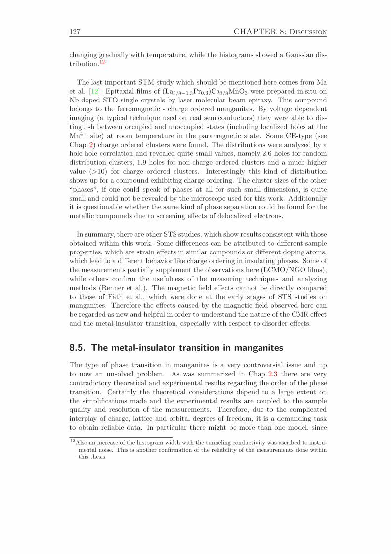
127 CHAPTER 8: Discussion
changing gradually with temperature, while the histograms showed a Gaussian dis-tribution.12
The last important STM study which should be mentioned here comes from Maet al. [12]. Epitaxial films of (La5/8−0.3Pr0.3)Ca3/8MnO3 were prepared in-situ onNb-doped STO single crystals by laser molecular beam epitaxy. This compoundbelongs to the ferromagnetic - charge ordered manganites. By voltage dependentimaging (a typical technique used on real semiconductors) they were able to dis-tinguish between occupied and unoccupied states (including localized holes at theMn4+ site) at room temperature in the paramagnetic state. Some CE-type (seeChap. 2) charge ordered clusters were found. The distributions were analyzed by ahole-hole correlation and revealed quite small values, namely 2.6 holes for randomdistribution clusters, 1.9 holes for non-charge ordered clusters and a much highervalue (>10) for charge ordered clusters. Interestingly this kind of distributionshows up for a compound exhibiting charge ordering. The cluster sizes of the other“phases”, if one could speak of phases at all for such small dimensions, is quitesmall and could not be revealed by the microscope used for this work. Additionallyit is questionable whether the same kind of phase separation could be found for themetallic compounds due to screening effects of delocalized electrons.
In summary, there are other STS studies, which show results consistent with thoseobtained within this work. Some differences can be attributed to different sampleproperties, which are strain effects in similar compounds or different doping atoms,which lead to a different behavior like charge ordering in insulating phases. Some ofthe measurements partially supplement the observations here (LCMO/NGO films),while others confirm the usefulness of the measuring techniques and analyzingmethods (Renner et al.). The magnetic field effects cannot be directly comparedto those of Fäth et al., which were done at the early stages of STS studies onmanganites. Therefore the effects caused by the magnetic field observed here canbe regarded as new and helpful in order to understand the nature of the CMR effectand the metal-insulator transition, especially with respect to disorder effects.
8.5. The metal-insulator transition in manganites
The type of phase transition in manganites is a very controversial issue and upto now an unsolved problem. As was summarized in Chap. 2.3 there are verycontradictory theoretical and experimental results regarding the order of the phasetransition. Certainly the theoretical considerations depend to a large extent onthe simplifications made and the experimental results are coupled to the samplequality and resolution of the measurements. Therefore, due to the complicatedinterplay of charge, lattice and orbital degrees of freedom, it is a demanding taskto obtain reliable data. In particular there might be more than one model, since
12Also an increase of the histogram width with the tunneling conductivity was ascribed to instru-mental noise. This is another confirmation of the reliability of the measurements done withinthis thesis.
8.5. The metal-insulator transition in manganites 128
the manganites might be very different as was already shown by the very richphase diagram (Fig. 2.12). At most it can be expected to find some explanationsfor special parts of the phase diagram, like the ferromagnetic compounds or thoseshowing charge ordering.
With the help of the results obtained in this work, it is possible to extend thefacts known so far to the very important issue of the metal-insulator transition in amagnetic field and contribute some considerations concerning the metal-insulatorand ferromagnetic-paramagnetic phase transition.
As was shown in this thesis, there are already differences within thin films on thesame substrates, grown under different deposition speeds (App. A). Fortunatelythe positive result is that – although the electronic transition changes locally – itbecame apparent for the whole series (from 3D over LL up to LL-O films) thatthe magnetic field changes the tunneling resistivity more or less uniformly all overthe samples and no distinct two phase behavior is present. The latter result mightspeak against a first-order transition, since a separation into two distinct phasesis not existent, and seems to be more appropriate for a continuous second ordertransition. On the other hand a first-order transition does not necessarily have toshow a phase separation.
The author suggests that the electronic transitions in manganites are coupledto their intrinsic nature, which might be very different. It might depend on theitinerancy of the electrons. The charge ordered manganites tend to show a firstorder like transition coupled with a phase separation. The latter is confirmed bythe experiments discussed above and for instance the new results from Wu et al.who found a glass like transition with a first-order nature by MFM measurementson La5/8−yPryCa3/8MnO3, y ≈ 0.4 [35]. Phase separation can only be predicted fora first-order transition and so far mainly the charge ordered compounds showed aclear phase separation. Since the non-existence of a phase separation on a nanome-ter scale below 2 nm cannot be clearly proven and the problem of a missing cleardefinition of the phases, a final determination of the nature of the transition isnot possible at this stage. Due to the tunable parameter-space in manganites it isprobably also impossible to clearly talk about the one or the other phase transitionwith exactly first or second order, it might be a mixture. There is no proof howthe Ginzburg-Landau formalism could be generalized to these materials.
The latter considerations are matching at least partially the generalized phasediagram from Littlewood et al. [13], shown in Fig. 8.9. The key parameter hereis the electron-phonon coupling. The authors claim that for a very weak couplingλ < λ0 a second-order phase transition without phase separation could be expected,while for a lager coupling λ > λ0 a discontinuous transition of first-order naturewith phase separation in the transition region is more probable. The white shadedregion is attributed to a possible (but not necessary) phase coexistence and theyellow shaded region is attributed to a second order phase transition, while theunshaded region corresponds to a first-order transition. The red lines denote first-order transitions between the phases, and therefore the observation for compoundswith charge ordering tendencies and ferromagnetic phases can be found in theregion of first-order phase transitions.
129 CHAPTER 8: Discussion
Electron−Phonon Coupling
FM−M
CO−I
PM
Tem
pe
ratu
re
λ0
Figure 8.9.: Phase transitions with temperature versus the electron phonon coupling parameterafter Littlewood et al. [13]. Red lines mark a first-order like transition. PM:paramagnetic region, FM-M: ferromagnetic metal, CO-I: charge ordered insulator.
On the one hand the films used here might be situated in the yellow shaded regionbelow λ0. A vivid discussion is still going on about the role of the polarons, but theelectron-phonon coupling could not be measured directly. The spectroscopy datashowed an itinerant electron behavior and no hints for a localization were foundon the length scales considered. The observations within magnetic fields confirm acontinuous change of the tunneling conductivity. On the other hand, the differentregions of gradually varying conductivity can be interpreted in terms of small vari-ations of strain fields within the films. In conclusion these different regions mighthave different transition temperatures TMI , which are highly dependent on the mi-crostructure, as was discussed above. These small inhomogeneities change theirconductivity continuously with respect to a magnetic field, but since the transitionvaries spatially over the film, the region pattern remains across the transition ofthe whole film. This leads to the broadening of the MIT for the 3D and LL filmscompared to the highly ordered LL-O film. The change in tunneling conductivityfor all regions can be explained by this local variation of TMI . From this point ofview also a distribution of many first-order phase transitions at slightly differenttemperatures in the different regions is also a possibility, provided that the sharpMIT for the LL-O film is of first-order nature without intrinsic phase separation.There are some weak hints for a first-order transition in the LL-O film, which needyet to be corroborated.
Of course it has to be taken into account that STS is a very local and surfacesensitive technique. Most people would expect nearly the same behavior for themanganites at the surface as in the bulk, but this is not absolutely clear. The STMcan detect more than a surface layer, but still mainly detects the surface propertiesat which the sample changes the geometry from a three-dimensional lattice to a two-

8.5. The metal-insulator transition in manganites 130
dimensional surface layer. The magneto resistance is the same for both samples,which was shown before, but the difference in the tunneling spectroscopy betweenthe samples, which were both examined nearby TMI , is evident.
As mentioned in Chap. 2.3, different experiments on the phase transition lead todifferent results concerning the order of the transition. The heat capacity measure-ments are not unambiguous and furthermore it is the question which parameterwould be the correct order parameter for manganites. At this point more work hasto be done to clarify this issue.
131 Bibliography
Bibliography
[1] K. H. Ahn, T. Lookman, and A. R. Bishop. Nature, 428:401, 2004.
[2] T. Becker. Untersuchung der elektrischen Phasenseparation in dünnen Man-
ganatschichten mit Rastersondenspektroskopie. Doktorarbeit, Universität Göt-tingen, 2004.
[3] T. Becker, C. Streng, Y. Luo, V. Moshnyaga, B. Damaschke, N. Shannon, andK. Samwer. Phys. Rev. Lett., 89:2372038, 2002.
[4] A. Biswas, M. Rajeswari, R. C. Srivastava, Y. H. Li, T. Venkatesan, R. L.Greene, and A. J. Millis. Phys. Rev. B, 61:9665, 2000.
[5] D. A. Bonnell. Prog. Surf. Sci., 57:187, 1998.
[6] S. F. Chen, P. I. Lin, J. Y. Juang, T. M. Uen, K. H. Wu, Y. S. Gou, and J. Y.Lin. Appl. Phys. Lett., 82:1242, 2003.
[7] M. Fäth, S. Freisem, A. A. Menovsky, Y. Tomioka, J. Aarts, and J. A. Mydosh.Science, 285:1540, 1999.
[8] M. Izumi, Y. Konishi, T. Nishihara, S. Hayaschi, M. Shinohara, M. Kawasaki,and Y. Tokura. Appl. Phys. Lett., 73:2497, 1998.
[9] S. Kar, J. Mitra, and A. K. Raychaudhuri. Solid stat. commun., 136:410, 2005.
[10] S. A. Köster, V. Moshnyaga, K. Samwer, O. Shapoval, A. Belenchuk, O. I.Lebedev, and G. van Tendeloo. Appl. Phys. Lett., 81:1648, 2002.
[11] N. Lang. Phys. Rev. Lett., 56:1164, 1986.
[12] J. X. Ma, D. T. Gillaspie, E. W. Plummer, and J. Shen. Phys. Rev. Lett.,95:237210, 2005.
[13] N. Mathur and P. Littlewood. Physics Today, 56:25, 2003.
[14] M. Mayr, A. Moreo, J. A. Verges, J. Arispe, A. Feiguin, and E. Dagotto. Phys.
Rev. Lett., 86:135, 2001.
[15] D. N. McIlroy, J. Zhang, S.-H. Liou, and P. A. Dowben. Phys. Lett. A, 207:367,1995.
[16] G. C. Milward, M. J. Calderón, and P. B. Littlewood. Nature, 433:607, 2005.
[17] J. Mitra, M. Paranjape, A. K. Raychaudhuri, N. D. Mathur, and M. G.Blamire. Phys. Rev. B, 71:094426, 2005.
[18] J. Mitra, M. Paranjape, A. K. Raychaudhuri, N. D. Mathur, and M. G.Blamire. Phys. Rev. B, 71:094426, 2005.
[19] A. Moreo, M. Mayr, A. Feiguin, S. Yunoki, and E. Dagotto. Phys. Rev. Lett.,84, 2000.
Bibliography 132
[20] V. Moshnyaga, B. Damaschke, O. Shapoval, A. Belenchuk, J. Faubel,O. I. Lebedev adn J. Verbeek, G. van Tendeloo, M. Müksch, V. Tsurkan,R. Tidecks, and K. Samwer. Nat. Mat., 2:247, 2003.
[21] V. Moshnyaga, L. Sudheendra, O. I. Lebedev, S. A. Köster, K. Gehrke,O. Shapoval, A. Belenchuk, B. Damaschke, G. van Tendeloo, and K. Samwer.Phys. Rev. Lett., 97:107205, 2006.
[22] W. E. Pickett and D. J. Singh. Phys. Rev. B, 53:1146, 1996.
[23] P. G. Radaelli, G. Iannone, M. Marezio, H. Y. Hwang, S.-W. Cheong, J. D.Jorgensen, and D. N. Argyriou. Phys. Rev. B, 56:8265, 1997.
[24] R. A. Rao, D. Lavric, T. K. Nath, and C. B. Eom. Appl. Phys. Lett., 73:3294,1998.
[25] R. A. Rao, D. Lavric, T. K. Nath, C. B. Eom, L. Wu, and F. Tsui. J. Appl.
Phys., 85:4794, 1999.
[26] Ch. Renner, G. Aeppli, B.-G. Kimm, U.-A. Soh, and S.-W. Cheong. Nature,416:518, 2002.
[27] Ch. Renner, G. Aeppli, and H. M. Rønnow. Mater. Sci. Eng. C, 25:775, 2005.
[28] P. Reutler, A. Bensaid, F. Herbstritt, C. Höfener, A. Marx, and R. Gross.Phys. Rev. B, 62:11619, 2000.
[29] H. M. Rønnow, Ch. Renner, G. Aeppli, T. Kimura, and Y. Tokura. Nature,440:1025, 2006.
[30] F. Sánchez, I. C. Infante, U. Lüders, Ll. Abad, and J. Fontcuberta. Surf. Sci.,600:1231, 2006.
[31] C. Şen, G. Alvarez, and E. Dagotto. Phys. Rev. Lett., 98:127202, 2007.
[32] J. Shin, S. V. Kalinin, H. N. Lee, H. M. Christen, R. G. Moore, E. W. Plummer,and A. P. Baddorf. Surf. Sci., 581:118, 2005.
[33] L. Sudheendra, V. Moshnyaga, E. D. Mishina, B. Damaschke, Th. Rasing, andK. Samwer. Phys. Rev. B, 75:172407, 2007.
[34] E. L. Wolff. Principles of Electron Tunneling Spectroscopy. Oxford UniversityPress, New York, 1985.
[35] W. Wu, C. Israel, N. Hur, S. Park, S.-W. Cheong, and A. de Lozanne. Nat.
mat., 5:881, 2006.
9. Summary and outlook
A lot of open questions still remain in manganite physics. The exact nature ofthe coupled metal-insulator and ferromagnetic-paramagnetic phase transition isunder debate. There are a lot of models, which consider a phase separation toexplain the large CMR effects, but it is not known if phase separation is a necessarycondition for such effects. A lot of bulk measurements lead to controversial resultswith respect to the nature of the transition, where they cannot exactly reveal themicroscopic mechanisms. Microscopic techniques are necessary to gain a deeperinsight into the local properties and how they are influenced by external parameters,like the temperature or a magnetic field.
In manganites structural, electronic and magnetic properties are strongly coupledto each other due to an interplay of charge, lattice and orbital degrees of freedom.The two competing exchange mechanisms, the super exchange (mainly responsiblefor antiferromagnetic coupling and localization) and the double exchange (provid-ing a ferromagnetic coupling and delocalization of the charge carriers) and a strongelectron lattice coupling are responsible for the metal-insulator and ferromagnetic-paramagnetic transition and the large CMR effect. A comprehensive picture hastherefore to include structural, electronic as well as magnetic information of thesystem. In this work scanning tunneling spectroscopy (STS) experiments on fer-romagnetic manganites provide detailed information on the local electronic prop-erties, while the macroscopic structure, transport and magnetization have beendetermined by standard techniques.
Different macroscopically strain-free films of La0.75Ca0.25MnO3 , deposited bythe MAD technique on MgO substrates, show a varying microscopic texture. Athree dimensional (3D) and layer by layer (LL) growth, depending on the depo-sition conditions, were observed. The 3D films showed the typical orthorhombicstructure, normally reported for LCMO films, while the LL films possess (the morepseudo-cubic like) rhombohedral structure coupled to an increased ordering of theA-site atoms [3]. The bulk properties like the resistivity and magnetization fol-low these observation in the sense that the electronic and magnetic transitions as afunction of temperature are broader for the 3D film connected with lower transitiontemperatures (Chap. 6).
The local tunneling conductivity was measured by STS, and two-dimensionaltunneling conductivity maps were generated for different temperatures and mag-netic fields below, but nearby the metal-insulator transition temperature. Withinthese STS maps regions with different tunneling conductivities were found, butall of them showed metallic like current-voltage characteristics and the differencesbetween the conductivities were small. The different regions were suggested to beattributable to uncompensated local strain fields in the films caused by disorder.The films could be quantified with respect to the disorder and the occurrence of
133
9.1. Future work 134
different regions. An ideally ordered film (not examined in this thesis) showedno different phases, while the size of different regions increased with supposedlyincreasing disorder from the LL to the 3D films.
The I(U) curves taken on differently conducting regions revealed a gradual in-crease of the tunneling conductivities with temperature and magnetic field nearbythe metal-insulator transition (Chap. 7). All regions increased their conductivityby more or less the same value. No two distinct phases were found and a sim-ple two-phase percolative model does not account for the ferromagnetic manganiteLa0.75Ca0.25MnO3 . A magnetic field induced increase of the density of states,which is depleted in the vicinity of the metal-insulator transition, was observed.No insulating gap was observed in the low conducting regions, in contrast to chargeordered manganites, see e.g. [4]. It can therefore be concluded, that a phase sepa-ration with two distinct conductivities, an insulating and metallic phase, cannot beconfirmed here at least on the observed length scales, although there is a tendencyto more pronounced phases for the more disordered film.
A first-order phase transition is believed to be appropriate for manganite com-pounds, which show charge ordering and a clear phase separation. For the ferro-magnetic compound La0.75Ca0.25MnO3 contradictory results regarding the phasetransition were presented in the literature. The results obtained here show a con-tinuous change of the tunneling conductivity with respect to magnetic fields. Theorder of the transition cannot be finally determined due to the quite sharp tran-sition in the resistivity for the LL-O film. The possibility of a distribution ofdifferent transition temperatures in the different regions (phases) coming up withthe disorder was suggested.
In a nutshell, the observed effects of magnetic fields on the local tunneling spec-troscopy together with the structural properties, revealed new aspects related to themetal-insulator transition in the ferromagnetic manganites. A percolative scenarioseems not to be a necessary prerequisite for the CMR. It provides a contributionto the understanding of the mechanisms being responsible for the adjacent colos-sal magneto resistive effect (CMR), which occurs mainly at the metal-insulatortransition region (Chap. 8). The nature of the phase transition cannot be finallyidentified, but by the microscopic technique a continuous change of the local elec-tronic properties by magnetic fields was visualized. A probable connection betweenthe electronic properties and (A-site) disorder was outlined.
9.1. Future work
It is possible to extend the picture given in this work to the local magnetic mo-ments. This could be achieved by means of spin-polarized measurements and oneof these is the spin-polarized scanning tunneling spectroscopy (SP-STS) [1], whichwas established by the group of M. Bode and W. Wulfhekel. With this techniqueit is possible to observe the spin-polarization of a surface very locally, down to theatomic scale.
For high resolution STM measurements, atomically flat surfaces are required andtherefore an appropriate surface preparation is needed, if the samples cannot be
135 CHAPTER 9: Summary and outlook
prepared in-situ by, for example, pulsed laser deposition. It is quite difficult tocleave such ferromagnetic perovskite manganites, since they do not have distinc-tive cleaving planes and normally end up with a quite rough surface. Thin filmsof extraordinarily high quality are the alternative, and some knowledge about therelationships between structural, electronic and magnetic properties is provided bythis work. The chemical composition and surface termination layers with possiblya reconstruction are not irrelevant. On this basis an extended study of the surfacelayers with, for instance, XPS and LEED would be important to find an adequatesurface preparation procedure, which does not destroy the surface and the intrinsicproperties of the manganite. Based on the first hints about the surfaces given inthe discussion, annealing under vacuum conditions with an oxygen partial pressuremight help to solve this problem.
Additional scanning probe measurements are of interest also on other manganitethin films, like Pr1−xCaxMnO3. On these films peculiar electric field effects wereobserved in the group of Ch. Jooss [5]. A first attempt to achieve some STM pic-tures on the highly insulating compound with x ≈ 0.3 was done within magneticfields (see App. B.1). Here the development of different phases under the influenceof a magnetic field would be very interesting, since a pronounced splitting intoinsulating and metallic phases is expected. Considering the observed electric fieldeffects, magnetic force microscopy (MFM) measurement could reveal the develop-ment of a current path. It can be expected that a current filament could be resolvedby its magnetic stray field. The latter would be an extraordinarily progress for theresearch within phase separation and percolation studies. A first MFM measure-ment is given in the appendix. Unfortunately these attempts were done on quiterough films, when the surface preparation was not as mature as it is now.
Another very interesting technique to observe the local spin configuration wouldbe spin-polarized electron energy loss spectroscopy (EELS). Of course, the resolu-tion is much less than for SP-STS, but it can reveal specific features on larger lengthscales, which could be compared to MFM measurements. This special techniqueis used within transmission electron microscopy, and can determine the spin-stateslocally and chemically resolved. It can also reveal other features, like specific mag-netic excitations as magnons. A much better understanding of such excitations,which possibly also occur in manganites and related materials, could be achieved.
Of course the field of manganite physics is much broader than the experimentspresented here. The optical and dynamic parts have been neglected, and onlyproposals directly related to this work were given. For instance, the dynamics inmanganites has not been explored very much so far. Mishina et al. [2] performedsecond-harmonic generation experiments and probed crystallographic and magneticeffects. The dynamic effects can reveal even more about the interplay of the spinand orbital degrees of freedom via the time scales of reaction. An idea, which cameup during this work, dealt about the performance of STS measurements under theoptical excitation of the sample by a laser.
While there are hundreds of publications about the general manganite proper-
Bibliography 136
ties, a detailed understanding of these materials still needs to be achieved. Furtherinvestigations will require more and more complex and local techniques and a verycareful sample preparation will be necessary. STS is one of these approaches con-sidering observations on a very local scale. Not very many groups can performSTS measurements together with magnetic fields and the results of this thesis haveshown, that there is still a great potential for manganite physics.
Bibliography
[1] M. Bode. Rep. Prog. Phys., 66:523, 2003.
[2] E. D. Mishina, A. I. Morosov, A. V. Mishina, V. Moshnyaga, L. Sudheendra,K. Samwer, and Th. Rasing. Phys. Rev. B, 75:0644401, 2007.
[3] V. Moshnyaga, L. Sudheendra, O. I. Lebedev, S. A. Köster, K. Gehrke,O. Shapoval, A. Belenchuk, B. Damaschke, G. van Tendeloo, and K. Samwer.Phys. Rev. Lett., 97:107205, 2006.
[4] Ch. Renner, G. Aeppli, B.-G. Kimm, U.-A. Soh, and S.-W. Cheong. Nature,416:518, 2002.
[5] W. Westhäuser, S. Schramm, J. Hoffmann, and Ch. Jooss. Eur. Phys. J. B,53:323, 2004.
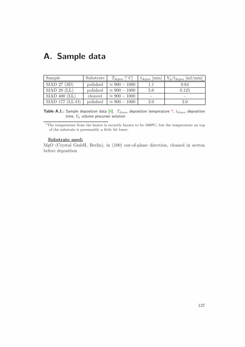
A. Sample data
Sample Substrate Tdepos [ C] tdepos [min] Vp/tdepos [ml/min]
MAD 27 (3D) polished ≈ 900 − 1000 1.1 0.64MAD 28 (LL) polished ≈ 900 − 1000 5.6 0.125MAD 400 (LL) cleaved ≈ 900 − 1000 - -MAD 177 (LL-O) polished ≈ 900 − 1000 2.0 2.0
Table A.1.: Sample deposition data [4]. Tdepos deposition temperature a, tdepos depositiontime, Vp volume precurser solution
aThe temperature from the heater is excactly known to be 1000, but the temperature on topof the substrate is presumably a little bit lower.
Substrate used:
MgO (Crystal GmbH, Berlin), in (100) out-of-plane direction, cleaned in acetonbefore deposition
137

138
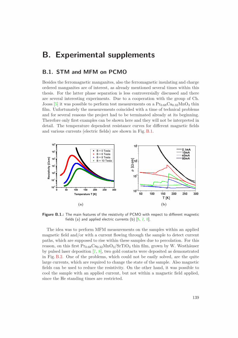
B. Experimental supplements
B.1. STM and MFM on PCMO
Besides the ferromagnetic manganites, also the ferromagnetic insulating and chargeordered manganites are of interest, as already mentioned several times within thisthesis. For the latter phase separation is less controversially discussed and thereare several interesting experiments. Due to a cooperation with the group of Ch.Jooss [5] it was possible to perform test measurements on a Pr0.68Ca0.32MnO3 thinfilm. Unfortunately the measurements coincided with a time of technical problemsand for several reasons the project had to be terminated already at its beginning.Therefore only first examples can be shown here and they will not be interpreted indetail. The temperature dependent resistance curves for different magnetic fieldsand various currents (electric fields) are shown in Fig. B.1.
0 50 100 150 200 250 30010-2
10-1
100
101
102
103
104
Res
istiv
ity [
cm]
Temperature T [K]
B = 0 TeslaB = 6 Tesla B = 8 TeslaB = 10 Tesla
(a) (b)
Figure B.1.: The main features of the resistivity of PCMO with respect to different magneticfields (a) and applied electric currents (b) [5, 7, 8].
The idea was to perform MFM measurements on the samples within an appliedmagnetic field and/or with a current flowing through the sample to detect currentpaths, which are supposed to rise within these samples due to percolation. For thisreason, on this first Pr0.68Ca0.32MnO3/SrTiO3 thin film, grown by W. Westhäuserby pulsed laser deposition [7, 8], two gold contacts were deposited as demonstratedin Fig. B.2. One of the problems, which could not be easily solved, are the quitelarge currents, which are required to change the state of the sample. Also magneticfields can be used to reduce the resistivity. On the other hand, it was possible tocool the sample with an applied current, but not within a magnetic field applied,since the He standing times are restricted.
139
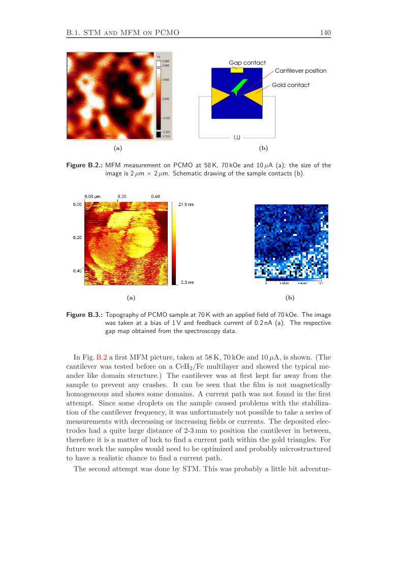
B.1. STM and MFM on PCMO 140
(a)
Gap contact
I,U
Cantilever position
Gold contact
(b)
Figure B.2.: MFM measurement on PCMO at 58 K, 70 kOe and 10µA (a); the size of theimage is 2µm × 2µm. Schematic drawing of the sample contacts (b).
(a) (b)
Figure B.3.: Topography of PCMO sample at 70 K with an applied field of 70 kOe. The imagewas taken at a bias of 1 V and feedback current of 0.2 nA (a). The respectivegap map obtained from the spectroscopy data.
In Fig. B.2 a first MFM picture, taken at 58 K, 70 kOe and 10µA, is shown. (Thecantilever was tested before on a CeH2/Fe multilayer and showed the typical me-ander like domain structure.) The cantilever was at first kept far away from thesample to prevent any crashes. It can be seen that the film is not magneticallyhomogeneous and shows some domains. A current path was not found in the firstattempt. Since some droplets on the sample caused problems with the stabiliza-tion of the cantilever frequency, it was unfortunately not possible to take a series ofmeasurements with decreasing or increasing fields or currents. The deposited elec-trodes had a quite large distance of 2-3 mm to position the cantilever in between,therefore it is a matter of luck to find a current path within the gold triangles. Forfuture work the samples would need to be optimized and probably microstructuredto have a realistic chance to find a current path.
The second attempt was done by STM. This was probably a little bit adventur-
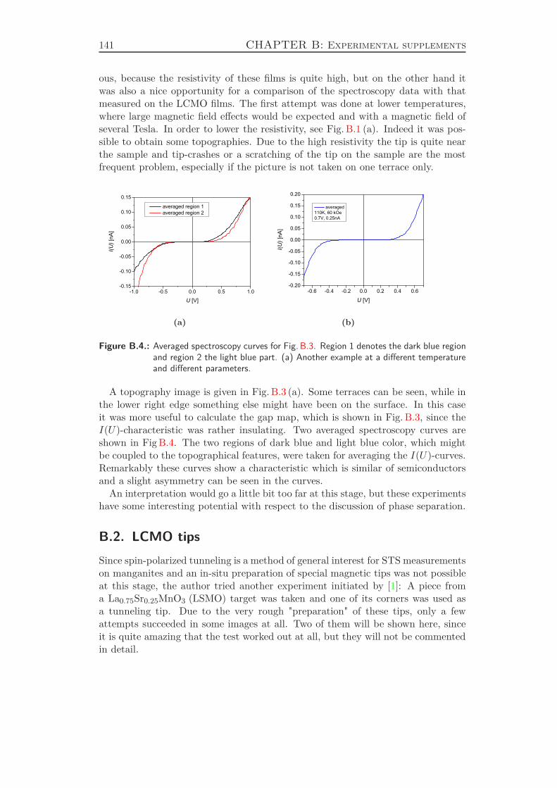
141 CHAPTER B: Experimental supplements
ous, because the resistivity of these films is quite high, but on the other hand itwas also a nice opportunity for a comparison of the spectroscopy data with thatmeasured on the LCMO films. The first attempt was done at lower temperatures,where large magnetic field effects would be expected and with a magnetic field ofseveral Tesla. In order to lower the resistivity, see Fig. B.1 (a). Indeed it was pos-sible to obtain some topographies. Due to the high resistivity the tip is quite nearthe sample and tip-crashes or a scratching of the tip on the sample are the mostfrequent problem, especially if the picture is not taken on one terrace only.
-1.0 -0.5 0.0 0.5 1.0-0.15
-0.10
-0.05
0.00
0.05
0.10
0.15
I(U) [
nA]
U [V]
averaged region 1 averaged region 2
(a)
-0.6 -0.4 -0.2 0.0 0.2 0.4 0.6-0.20
-0.15
-0.10
-0.05
0.00
0.05
0.10
0.15
0.20
I(U) [
nA]
U [V]
averaged110K, 60 kOe0.7V, 0.25nA
(b)
Figure B.4.: Averaged spectroscopy curves for Fig. B.3. Region 1 denotes the dark blue regionand region 2 the light blue part. (a) Another example at a different temperatureand different parameters.
A topography image is given in Fig. B.3 (a). Some terraces can be seen, while inthe lower right edge something else might have been on the surface. In this caseit was more useful to calculate the gap map, which is shown in Fig. B.3, since theI(U)-characteristic was rather insulating. Two averaged spectroscopy curves areshown in Fig B.4. The two regions of dark blue and light blue color, which mightbe coupled to the topographical features, were taken for averaging the I(U)-curves.Remarkably these curves show a characteristic which is similar of semiconductorsand a slight asymmetry can be seen in the curves.
An interpretation would go a little bit too far at this stage, but these experimentshave some interesting potential with respect to the discussion of phase separation.
B.2. LCMO tips
Since spin-polarized tunneling is a method of general interest for STS measurementson manganites and an in-situ preparation of special magnetic tips was not possibleat this stage, the author tried another experiment initiated by [1]: A piece froma La0.75Sr0.25MnO3 (LSMO) target was taken and one of its corners was used asa tunneling tip. Due to the very rough "preparation" of these tips, only a fewattempts succeeded in some images at all. Two of them will be shown here, sinceit is quite amazing that the test worked out at all, but they will not be commentedin detail.
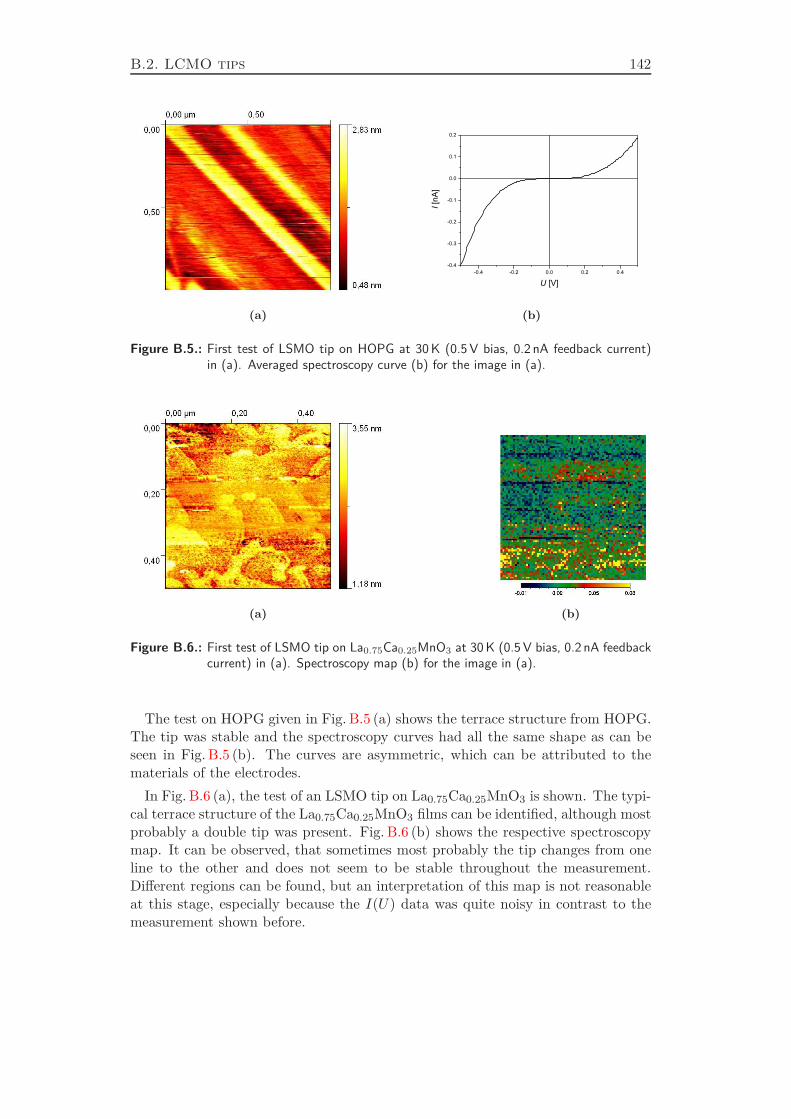
B.2. LCMO tips 142
(a)
-0.4 -0.2 0.0 0.2 0.4-0.4
-0.3
-0.2
-0.1
0.0
0.1
0.2
I [nA
]
U [V]
(b)
Figure B.5.: First test of LSMO tip on HOPG at 30 K (0.5 V bias, 0.2 nA feedback current)in (a). Averaged spectroscopy curve (b) for the image in (a).
(a) (b)
Figure B.6.: First test of LSMO tip on La0.75Ca0.25MnO3 at 30 K (0.5 V bias, 0.2 nA feedbackcurrent) in (a). Spectroscopy map (b) for the image in (a).
The test on HOPG given in Fig. B.5 (a) shows the terrace structure from HOPG.The tip was stable and the spectroscopy curves had all the same shape as can beseen in Fig. B.5 (b). The curves are asymmetric, which can be attributed to thematerials of the electrodes.
In Fig. B.6 (a), the test of an LSMO tip on La0.75Ca0.25MnO3 is shown. The typi-cal terrace structure of the La0.75Ca0.25MnO3 films can be identified, although mostprobably a double tip was present. Fig. B.6 (b) shows the respective spectroscopymap. It can be observed, that sometimes most probably the tip changes from oneline to the other and does not seem to be stable throughout the measurement.Different regions can be found, but an interpretation of this map is not reasonableat this stage, especially because the I(U) data was quite noisy in contrast to themeasurement shown before.
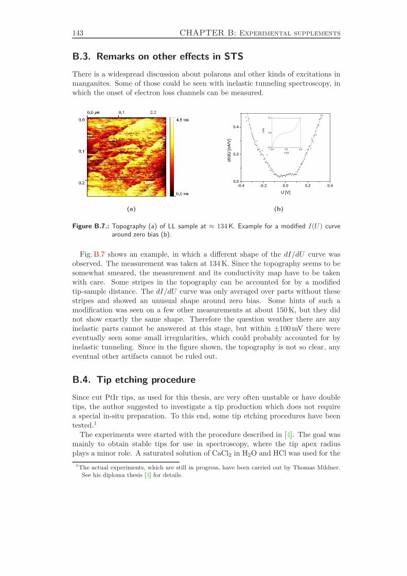
143 CHAPTER B: Experimental supplements
B.3. Remarks on other effects in STS
There is a widespread discussion about polarons and other kinds of excitations inmanganites. Some of those could be seen with inelastic tunneling spectroscopy, inwhich the onset of electron loss channels can be measured.
(a)
-0.4 0.0 0.4-0.1
0.0
0.1
-0.4 -0.2 0.0 0.2 0.40.0
0.2
0.4
dI/d
U [n
A/V
]
U [V]
I [nA
]
U [V]
(b)
Figure B.7.: Topography (a) of LL sample at ≈ 134 K. Example for a modified I(U) curvearound zero bias (b).
Fig. B.7 shows an example, in which a different shape of the dI/dU curve wasobserved. The measurement was taken at 134 K. Since the topography seems to besomewhat smeared, the measurement and its conductivity map have to be takenwith care. Some stripes in the topography can be accounted for by a modifiedtip-sample distance. The dI/dU curve was only averaged over parts without thesestripes and showed an unusual shape around zero bias. Some hints of such amodification was seen on a few other measurements at about 150 K, but they didnot show exactly the same shape. Therefore the question weather there are anyinelastic parts cannot be answered at this stage, but within ±100 mV there wereeventually seen some small irregularities, which could probably accounted for byinelastic tunneling. Since in the figure shown, the topography is not so clear, anyeventual other artifacts cannot be ruled out.
B.4. Tip etching procedure
Since cut PtIr tips, as used for this thesis, are very often unstable or have doubletips, the author suggested to investigate a tip production which does not requirea special in-situ preparation. To this end, some tip etching procedures have beentested.1
The experiments were started with the procedure described in [4]. The goal wasmainly to obtain stable tips for use in spectroscopy, where the tip apex radiusplays a minor role. A saturated solution of CaCl2 in H2O and HCl was used for the
1The actual experiments, which are still in progress, have been carried out by Thomas Mildner.See his diploma thesis [3] for details.
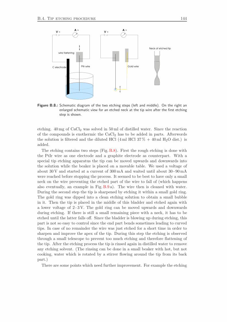
B.4. Tip etching procedure 144
PtIr wire Gold wire
solution
C electrode
wire fastening
Neck of etched tip
A ~V ~
A ~V ~
Figure B.8.: Schematic diagram of the two etching steps (left and middle). On the right anenlarged schematic view for an etched neck at the tip wire after the first etchingstep is shown.
etching. 40 mg of CaCl2 was solved in 50 ml of distilled water. Since the reactionof the compounds is exothermic the CaCl2 has to be added in parts. Afterwordsthe solution is filtered and the diluted HCl (4 ml HCl 37 % + 40 ml H2O dist.) isadded.
The etching contains two steps (Fig. B.8). First the rough etching is done withthe PtIr wire as one electrode and a graphite electrode as counterpart. With aspecial tip etching apparatus the tip can be moved upwards and downwards intothe solution while the beaker is placed on a movable table. We used a voltage ofabout 30 V and started at a current of 300 mA and waited until about 30 - 90 mAwere reached before stopping the process. It seemed to be best to have only a smallneck on the wire preventing the etched part of the wire to fall of (which happensalso eventually, an example in Fig. B.9 a). The wire then is cleaned with water.During the second step the tip is sharpened by etching it within a small gold ring.The gold ring was dipped into a clean etching solution to obtain a small bubblein it. Then the tip is placed in the middle of this bladder and etched again witha lower voltage of 2 - 3 V. The gold ring can be moved upwards and downwardsduring etching. If there is still a small remaining piece with a neck, it has to beetched until the latter falls off. Since the bladder is blowing up during etching, thispart is not so easy to control since the end part bends sometimes leading to curvedtips. In case of no remainder the wire was just etched for a short time in order tosharpen and improve the apex of the tip. During this step the etching is observedthrough a small telescope to prevent too much etching and therefore flattening ofthe tip. After the etching process the tip is rinsed again in distilled water to removeany etching solvent. (The rinsing can be done in a small beaker with hot, but notcooking, water which is rotated by a stirrer flowing around the tip from its backpart.)
There are some points which need further improvement. For example the etching
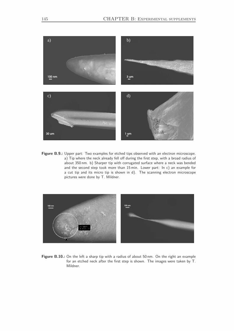
145 CHAPTER B: Experimental supplements
b)
1 um30 um
c) d)
3 um100 nm
a)
Figure B.9.: Upper part: Two examples for etched tips observed with an electron microscope.a) Tip where the neck already fell off during the first step, with a broad radius ofabout 350 nm. b) Sharper tip with corrugated surface where a neck was bendedand the second step took more than 15 min. Lower part: In c) an example fora cut tip and its micro tip is shown in d). The scanning electron microscopepictures were done by T. Mildner.
100 um100 nm
Figure B.10.: On the left a sharp tip with a radius of about 50 nm. On the right an examplefor an etched neck after the first step is shown. The images were taken by T.Mildner.
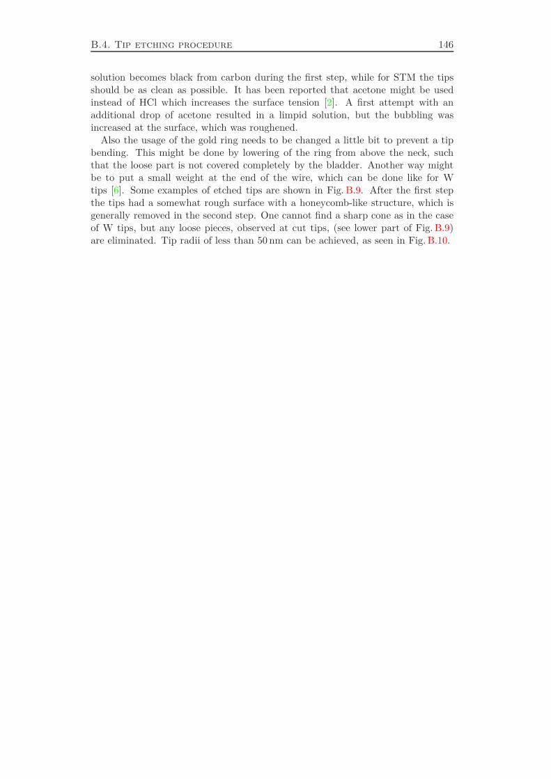
B.4. Tip etching procedure 146
solution becomes black from carbon during the first step, while for STM the tipsshould be as clean as possible. It has been reported that acetone might be usedinstead of HCl which increases the surface tension [2]. A first attempt with anadditional drop of acetone resulted in a limpid solution, but the bubbling wasincreased at the surface, which was roughened.
Also the usage of the gold ring needs to be changed a little bit to prevent a tipbending. This might be done by lowering of the ring from above the neck, suchthat the loose part is not covered completely by the bladder. Another way mightbe to put a small weight at the end of the wire, which can be done like for Wtips [6]. Some examples of etched tips are shown in Fig. B.9. After the first stepthe tips had a somewhat rough surface with a honeycomb-like structure, which isgenerally removed in the second step. One cannot find a sharp cone as in the caseof W tips, but any loose pieces, observed at cut tips, (see lower part of Fig. B.9)are eliminated. Tip radii of less than 50 nm can be achieved, as seen in Fig. B.10.

147 Bibliography
Bibliography
[1] R. Akiyama, H. Tanaka, T. Matsumoto, and T. Kawai. Appl. Phys. Lett.,79:4387, 2001.
[2] L. Libioulle, Y. Houbion, and J.-M. Gilles. J. Vac. Sci. Technol. B, 3:1325,1995.
[3] T. Mildner. Diplomarbeit, Universität Göttingen.
[4] I. H. Musselman and P. E. Russell. J. Vac. Sci. Technol. A, 4:3558, 1990.
[5] Group PD Dr. Ch. Jooss. University of Göttingen, Institut für Materialphysik,http://www.material.physik.uni-goettingen.de.
[6] C. Streng. Wachstumsanalyse amorpher dicker Schichten und Schichsysteme.Doktorarbeit, University of Göttingen, 2004.
[7] W. Westhäuser. Transporteigentschaften von Manganat-Filmen in magnetis-chen und elektrischen Feldern am Beispiel von Pr0.68Ca0.32MnO3. Diplomar-beit, Universität Göttingen, 2004.
[8] W. Westhäuser, S. Schramm, and Ch. Jooss. Europ. J. Phys. B, 53:323, 2006.

Bibliography 148
C. Mathematical considerations
C.1. Autocorrelation function
The autocorrelation function, which can be used, e.g. for comparing structureswithin an image, constitutes a self-correlation and can be calculated via two di-mensional Fourier transforms [2]. The correlation C(x) of two complex functionsis defined similar to a convolution as
Cfg(x) = f(x) ∗ g(x) =∫ +∞
−∞f∗(u)g(u + x)du (C.1)
and the autocorrelation is defined as
C(x) = Cff (x) = f(x) ∗ f(x) =∫ +∞
−∞f∗(u)f(u+ x)du (C.2)
which is also called an auto-covariance function. The two dimensional autocorre-lation function is defined completely analogously. For a calculation the Wiener-Khinchine-Theorem is applied, that is the autocorrelation can be calculated viathe inverse Fourier transform1 F−
F− [f ∗ f ] = f∗f =∣
∣
∣f2∣
∣
∣ . (C.3)
Normally the measurements only exist as a limited amount of data points, sothat the discrete form of the Fourier transform has to be used. To discretize theFourier transform one either uses the sampling theorem or imagines it convolvedwith a box function (for the reduction of values into a pixel), then multiplied witha comb function (for the discretization) and again convolved with a box function(for the limited data range, which cannot be infinite). The reader is referred to[2] for more details on the formalism. As the result, both data spaces consist oflimited and discretized values
fl =1N
N−1∑
j=0
fj exp(
−2πijl
N
)
(C.4)
and the respective inverse form. One thus gets a system of N linear equations withN summands, which could be written in matrix form. The matrix itself can in turnbe decomposed into small matrices, which are easier to calculate, and this leadsto the fast Fourier transform FFT, which is normally used by the programminglanguages like IDL [1].
1The operator F± stands for the integration over the argument of the function and the sign corre-sponds to the sign in the exponential function. F+
[
f(s)]
= f(x) =∫ +∞
−∞f(s) exp (+2πisx)dx.
149

Bibliography 150
Bibliography
[1] IDL – Interactive data language. Research Systems, Inc. Version 6.0.
[2] W. H. Press, S. A. Teukolsky, W. T. Vetterling, and B. P. Flannery. Numerical
Recipes in C. Cambridge University Press, 1992.
Acknowledgement
At the end of this thesis I would like to take the pleasant duty to express mygratitude to the people who accompanied me during the last years in the scientificand personal background of this work.
I would like to thank . . .
. . . first of all Professor Konrad Samwer for his mentoring and lots of discussionswhich he managed to accomplish besides all his duties at university and the oppor-tunity to write a thesis in a challenging field of solid state physics.
. . . Dr. Bernd Damaschke for his help in particular with the programming (thereis a language without punctuation) and the great coffee from his very special coffeemachine (being always at our service).
. . . PD Dr. Christian Jooss for being second referee and for participating in ourmanganite project with his group, which enriched the seminars and discussions.
. . . Juniorprofessor Stefan Mayr for providing his correlation analysis program(see you next night at the institute).
. . . Dr. Steffen Wirth at the MPI in Dresden for the first try at very low temper-atures and discussions about STM measurements on manganites.
. . . Dr. Volker Neu and Dr. Ulrike Wolff at the IFW in Dresden for (also mental)support regarding technical matters concerning the Cryogenic SFM (yes, it has itsown personality).
. . . the manganite group, especially PD Dr. Vasily Moshnyaga and Dr. LakshamaSudheendra. There have been many fruitful discussions, numerous interesting sem-inars about manganites and many informative talks about other cultures.
. . . Thomas Mildner for exploring the tip etching world.
. . . all the people around. The years at the institute were very instructive andtherefore I thank Juniorprofessor Stefan Mayr, Henrike Neubauer, Iris Kock, TobiasEdler, Uta Bete, Guido Mahnke and all the others for the get-together’s and chatsduring the coffee breaks, walking-tours on external institute seminars and holdingthe fort in the sacred halls of the new physics department during uncommon work-ing hours.
. . . the group around Dr. Martin Wenderoth for being very kind lab neighbors.
. . . our secretaries Alexandra Lüttich and Regina Hühne, who keep the institute

and projects going on the organizational side.
. . . Hartmut Eichenberg and Elmar Gatzemeier for the commitment of the work-shop and Katrin Gehrke for the friendly help with the laboratory issues (nothingworks without technical realization) and our systems administrator Carsten Mahn.
. . . the Deutsche Forschungsgemeinschaft for financial support.
. . . Dr. Christian Hettlage and Christian Tusche for a painstaking proof-readingand keeping me up at work.
. . . Christian Tusche for the many fruitful discussions about physics.
. . . the university Aikido group, which gave me a great opportunity to balancethe office days (nothing goes beyond momentum and energy conservation) and toget to know very friendly people.
. . . Dr. Edith Kirsch-Auwärter and Dr. Sylke Ernst for delivering me some in-sight into the matters and politics outside scientific questions.
. . . Dr. Christian Hettlage for the many years of friendship in and outside thephysics world (always take a towel, just in case).
. . . my friends Kai Nörthemann, Diana Marcano, Salvatore Manmana, WolfgangVukovich, Cathrin Hühne, Jeroen Custers, Kathrin, Sven and little Anna, Christian(B.), Roswitha, Georg, Axel and Heike for their company. Also many thanks tomy parents as well as Ernst and Helga Harmening.
I am deeply grateful for the understanding and never-ending patience from Klaus.
Curriculum Vitae
Personliche Daten
Name: Sigrun Antje Koster
Geburtsdatum: 25. November 1975
Geburtsort: Braunschweig
Universitat
seit 2003 Promotion
2001–2002 Diplomarbeit, ”Anderung der Magnetowiderstandseffekte in La0.7Sr0.3MnO3-
Filmen durch Dotierung der Korngrenzen mit MgO”, I. Physikalisches
Institut, Universitat Gottingen
1998–1999 Stipendium: University of California San Diego, USA
1998 Vordiplom
1996–2002 Physikstudium, Universitat Gottingen und University of California
1995–1996 Chemiestudium, Universitat Gottingen
Schule
1995 Abitur
1988–1995 Gymnasium Gaußschule, Braunschweig
1986–1988 Orientierungsstufe Ruhme, Braunschweig
1982–1986 Grundschule Waggum, Braunschweig