Embed Size (px)
Citation preview
Mixed Mode Simulation
Florian Erdinger (P. Fischer)
Lehrstuhl für Schaltungstechnik und SimulationTechnische Informatik der Uni Heidelberg
VLSI Design - Mixed Mode Simulation © F. Erdinger, ZITI, Uni Heidelberg Page 1
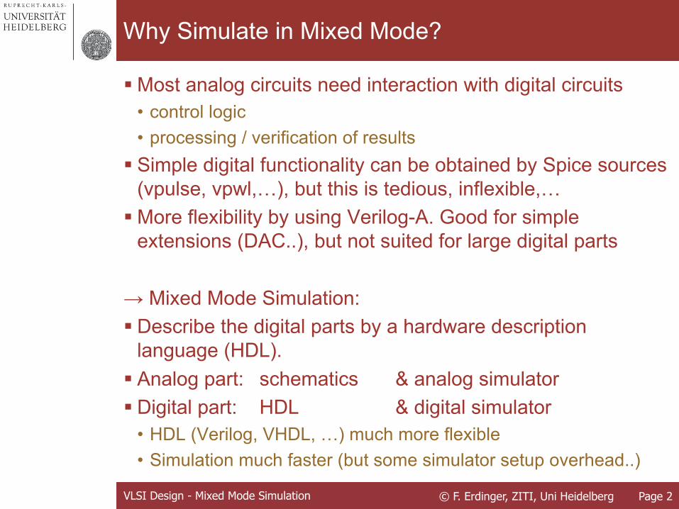
Why Simulate in Mixed Mode?
§ Most analog circuits need interaction with digital circuits• control logic• processing / verification of results
§ Simple digital functionality can be obtained by Spice sources (vpulse, vpwl,…), but this is tedious, inflexible,…
§ More flexibility by using Verilog-A. Good for simple extensions (DAC..), but not suited for large digital parts
→ Mixed Mode Simulation:§ Describe the digital parts by a hardware description
language (HDL).§ Analog part: schematics & analog simulator§ Digital part: HDL & digital simulator
• HDL (Verilog, VHDL, …) much more flexible• Simulation much faster (but some simulator setup overhead..)
VLSI Design - Mixed Mode Simulation © F. Erdinger, ZITI, Uni Heidelberg Page 2
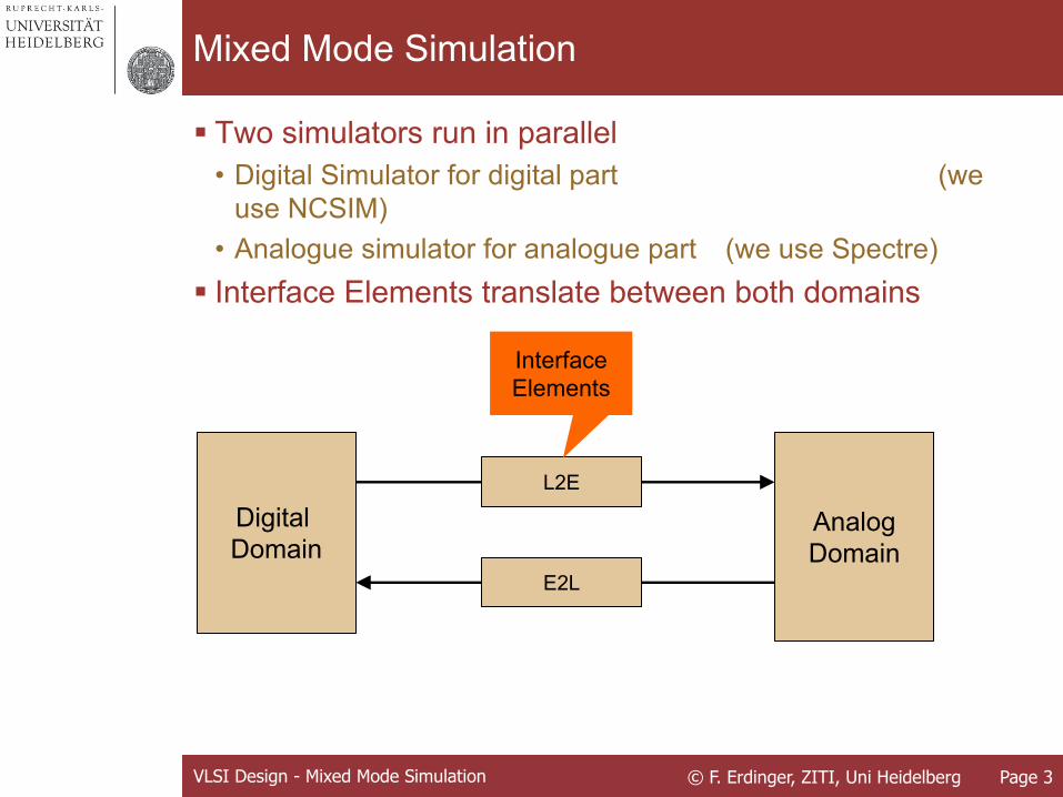
Mixed Mode Simulation
§ Two simulators run in parallel• Digital Simulator for digital part (we
use NCSIM)• Analogue simulator for analogue part (we use Spectre)
§ Interface Elements translate between both domains
AnalogDomain
Digital Domain
L2E
E2L
VLSI Design - Mixed Mode Simulation © F. Erdinger, ZITI, Uni Heidelberg Page 3
Interface Elements
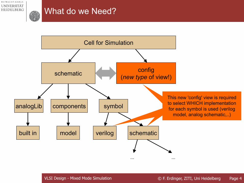
What do we Need?
schematic config(new type of view!)
Cell for Simulation
verilog
symbolcomponentsanalogLib
schematicmodel
VLSI Design - Mixed Mode Simulation © F. Erdinger, ZITI, Uni Heidelberg Page 4
This new type of view is required to select, WHICH implementation
for a symbol is used (verilog model, analog schematic,..)
This new type of view is required to select, WHICH implementation
for a symbol is used (verilog model, analog schematic,..)
This new 'config' view is required to select WHICH implementationfor each symbol is used (verilog
model, analog schematic,..)
built in
… …
A SIMPLE EXAMPLE
A Simple Example
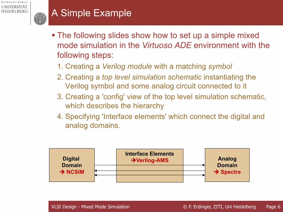
§ The following slides show how to set up a simple mixed mode simulation in the Virtuoso ADE environment with the following steps:1. Creating a Verilog module with a matching symbol2. Creating a top level simulation schematic instantiating the
Verilog symbol and some analog circuit connected to it3. Creating a 'config' view of the top level simulation schematic,
which describes the hierarchy4. Specifying 'Interface elements' which connect the digital and
analog domains.
VLSI Design - Mixed Mode Simulation © F. Erdinger, ZITI, Uni Heidelberg Page 6
Interface ElementsàVerilog-AMS Analog
Domainà Spectre
Digital Domainà NCSIM
Before You Start
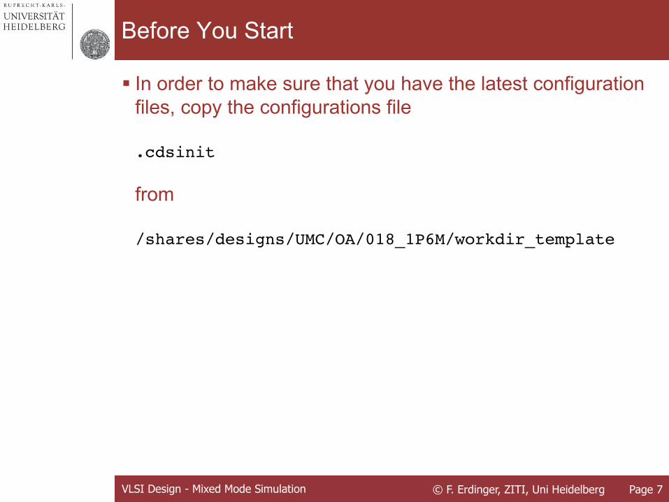
§ In order to make sure that you have the latest configuration files, copy the configurations file
.cdsinit
from
/shares/designs/UMC/OA/018_1P6M/workdir_template
VLSI Design - Mixed Mode Simulation © F. Erdinger, ZITI, Uni Heidelberg Page 7
1. Creating a New Verilog Module
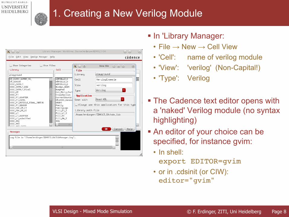
§ In 'Library Manager:• File → New → Cell View• 'Cell': name of verilog module• 'View': 'verilog' (Non-Capital!)• 'Type': Verilog
§ The Cadence text editor opens with a 'naked' Verilog module (no syntax highlighting)
§ An editor of your choice can be specified, for instance gvim:• In shell:export EDITOR=gvim
• or in .cdsinit (or CIW):editor="gvim"
VLSI Design - Mixed Mode Simulation © F. Erdinger, ZITI, Uni Heidelberg Page 8
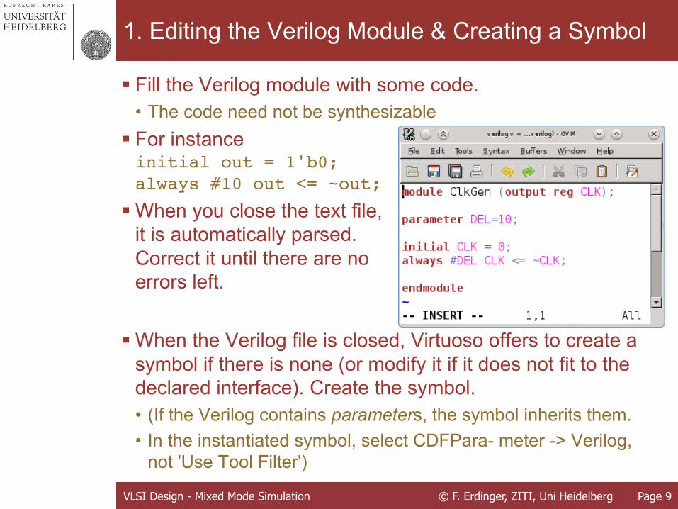
1. Editing the Verilog Module & Creating a Symbol
§ Fill the Verilog module with some code.• The code need not be synthesizable
§ For instanceinitial out = 1'b0;always #10 out <= ~out;
§ When you close the text file,it is automatically parsed.Correct it until there are noerrors left.
§ When the Verilog file is closed, Virtuoso offers to create a symbol if there is none (or modify it if it does not fit to the declared interface). Create the symbol.• (If the Verilog contains parameters, the symbol inherits them.• In the instantiated symbol, select CDFPara- meter -> Verilog,
not 'Use Tool Filter')
VLSI Design - Mixed Mode Simulation © F. Erdinger, ZITI, Uni Heidelberg Page 9
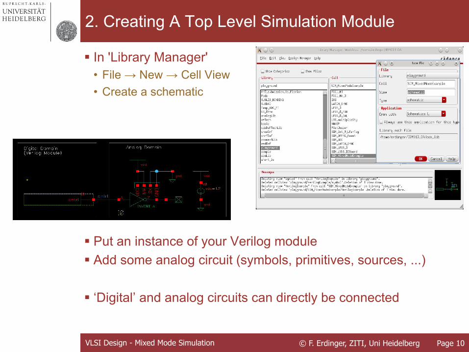
§ In 'Library Manager'• File → New → Cell View• Create a schematic
§ Put an instance of your Verilog module§ Add some analog circuit (symbols, primitives, sources, ...)
§ ‘Digital’ and analog circuits can directly be connected
2. Creating A Top Level Simulation Module
VLSI Design - Mixed Mode Simulation © F. Erdinger, ZITI, Uni Heidelberg Page 10
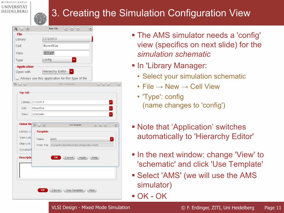
3. Creating the Simulation Configuration View
§ The AMS simulator needs a 'config' view (specifics on next slide) for the simulation schematic
§ In 'Library Manager:• Select your simulation schematic• File → New → Cell View• 'Type': config
(name changes to 'config')
§ Note that ‘Application’ switches automatically to 'Hierarchy Editor'
§ In the next window: change 'View' to 'schematic' and click 'Use Template'
§ Select 'AMS' (we will use the AMS simulator)
§ OK - OKVLSI Design - Mixed Mode Simulation © F. Erdinger, ZITI, Uni Heidelberg Page 11
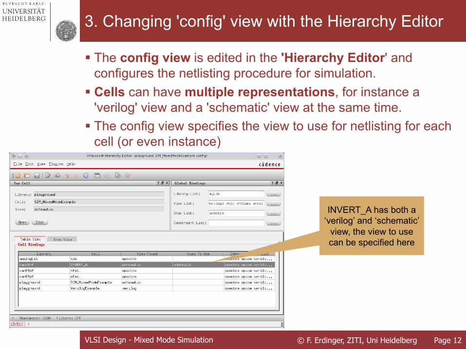
3. Changing 'config' view with the Hierarchy Editor
§ The config view is edited in the 'Hierarchy Editor' and configures the netlisting procedure for simulation.
§ Cells can have multiple representations, for instance a 'verilog' view and a 'schematic' view at the same time.
§ The config view specifies the view to use for netlisting for each cell (or even instance)
INVERT_A has both a ‘verilog’ and ‘schematic’
view, the view to use can be specified here
VLSI Design - Mixed Mode Simulation © F. Erdinger, ZITI, Uni Heidelberg Page 12
4. Adding the Interface Elements
§ There are built-in Interface Elements (IE) supplied with the simulator (which can also be customized if necessary)
§ They are located in the ‘connectLib’§ To add the connectLib to your library path
• In the Library Manager: Edit → Library Path…• In the table add a row with
Library = connectLibPath = /opt/eda/INCISIVE142/tools.lnx86/affirma_ams/etc/connect_lib/connectLib
• (this must only be done once, library definition is saved in .cdslib)
§ The IEs to be used are selected in the ADE when setting up the simulation (specifics see later)
§ They are inserted automatically (do not have to be placed in the schematic manually)
VLSI Design - Mixed Mode Simulation © F. Erdinger, ZITI, Uni Heidelberg Page 13
Setting Up the Simulation and Outputs
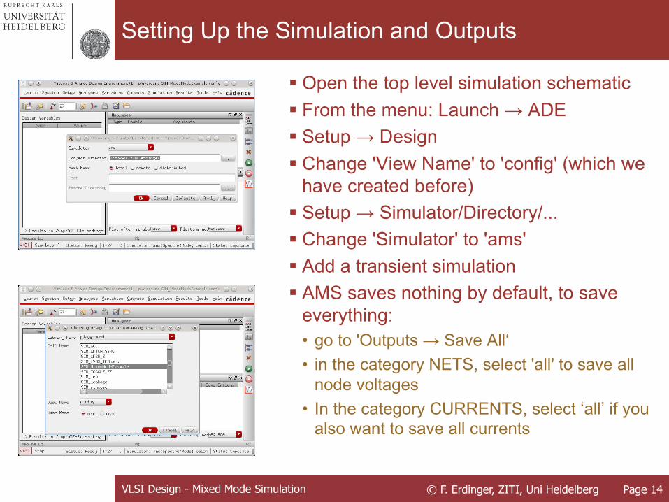
§ Open the top level simulation schematic§ From the menu: Launch → ADE§ Setup → Design § Change 'View Name' to 'config' (which we
have created before)§ Setup → Simulator/Directory/...§ Change 'Simulator' to 'ams'§ Add a transient simulation§ AMS saves nothing by default, to save
everything:• go to 'Outputs → Save All‘• in the category NETS, select 'all' to save all
node voltages• In the category CURRENTS, select ‘all’ if you
also want to save all currents
VLSI Design - Mixed Mode Simulation © F. Erdinger, ZITI, Uni Heidelberg Page 14
Specifying the Interface Elements
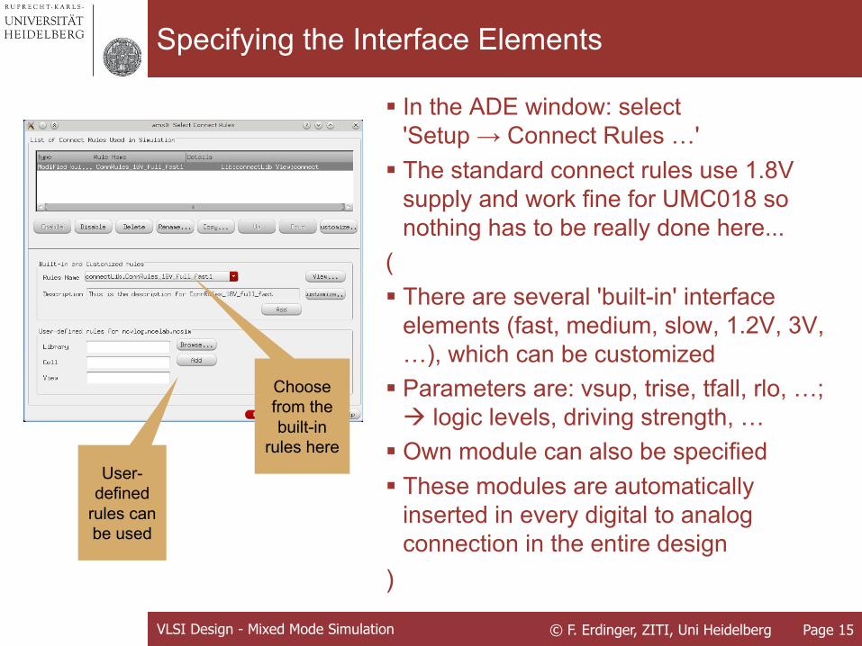
§ In the ADE window: select 'Setup → Connect Rules …'
§ The standard connect rules use 1.8V supply and work fine for UMC018 so nothing has to be really done here...
(§ There are several 'built-in' interface
elements (fast, medium, slow, 1.2V, 3V, …), which can be customized
§ Parameters are: vsup, trise, tfall, rlo, …;à logic levels, driving strength, …
§ Own module can also be specified§ These modules are automatically
inserted in every digital to analog connection in the entire design
)
Choose from the built-in
rules hereUser-
defined rules can be used
VLSI Design - Mixed Mode Simulation © F. Erdinger, ZITI, Uni Heidelberg Page 15
Viewing and Customizing the Interface Elements
(This is for information only..)
VLSI Design - Mixed Mode Simulation © F. Erdinger, ZITI, Uni Heidelberg Page 16
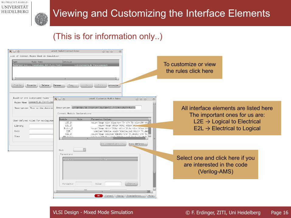
To customize or view the rules click here
All interface elements are listed hereThe important ones for us are:
L2E → Logical to ElectricalE2L → Electrical to Logical
Select one and click here if you are interested in the code
(Verilog-AMS)
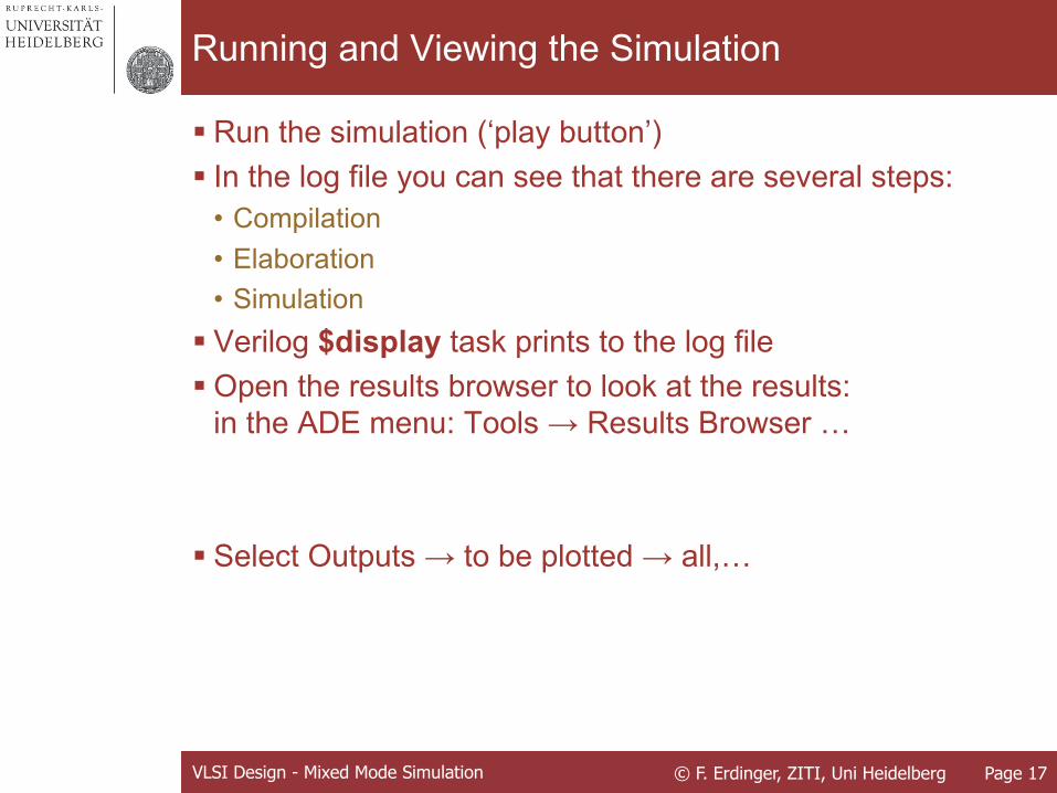
Running and Viewing the Simulation
§ Run the simulation (‘play button’) § In the log file you can see that there are several steps:
• Compilation• Elaboration• Simulation
§ Verilog $display task prints to the log file§ Open the results browser to look at the results:
in the ADE menu: Tools → Results Browser …
§ Select Outputs → to be plotted → all,…
VLSI Design - Mixed Mode Simulation © F. Erdinger, ZITI, Uni Heidelberg Page 17
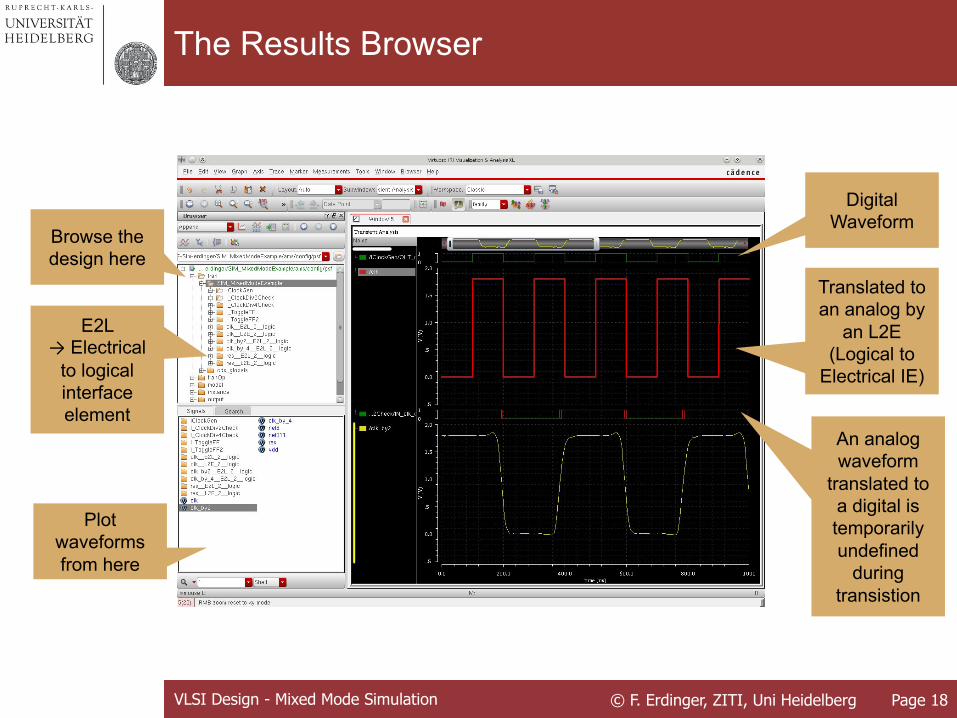
The Results Browser
Browse the design here
E2L → Electrical
to logical interface element
Digital Waveform
Translated toan analog by
an L2E (Logical to
Electrical IE)
An analog waveform
translated to a digital is temporarily undefined
during transistion
Plot waveforms from here
VLSI Design - Mixed Mode Simulation © F. Erdinger, ZITI, Uni Heidelberg Page 18
EXERCISE: MIXED MODE SIMULATION
Exercise: Clock Generation and Division
§ Step 1: Create a ‘ClockGenerator’ cell• Generate a Verilog view • If you want, parameterize the clock frequency
(Parameters can be overwritten in the properties of the schematic instance, change the ‘CDF Parameter view’ combo box to ‘verilog’)
• Follow all steps until you have the symbol§ Step 2: Create a new schematic (for simulation)
• Instantiate the ClockGenerator• Use your flip-flop from exercise 4 to divide the clock signal by 2
§ Step 3: Mixed mode simulation• Follow all described steps to setup and run a mixed mode
simulation• Browse through the results
VLSI Design - Mixed Mode Simulation © F. Erdinger, ZITI, Uni Heidelberg Page 20
Exercise: Check that the divider works
§ Step 4: Make a ‘ClockChecker’ cell• Make a Verilog module which has a clock and a divided clock
input • Use Verilog code to verify that the clock is divided correctly• Try to use a parameter for the division check• Use a second flip flop to divide by 4, use the parameter to adjust
the division check
§ NOTE: When re-running the simulation, the results in the lower hierarchy might be missing despite for ‘save all’.→ Closing and re-opening the results browser should fix this.
VLSI Design - Mixed Mode Simulation © F. Erdinger, ZITI, Uni Heidelberg Page 21


![HMO3004 - farnell.com · HMO3004 Serie 4-Kanal Mixed-Signal-Oszilloskope HMO3002 Serie 2-Kanal Mixed-Signal-Oszilloskope HMO3032 [HMO3034] 300 MHz](https://img.pdfslide.org/doc/110x75/5e0fe9d4d38f1d4fce090348/hmo3004-hmo3004-serie-4-kanal-mixed-signal-oszilloskope-hmo3002-serie-2-kanal.jpg)