Embed Size (px)
Citation preview
myAVRmyAVRmyAVRmyAVR
www.myAVR.de © Laser & Co. Solutions GmbH – 06/2009 www.myAVR.com
Technische Beschreibung technical description
myAVR Board MK3 3.10
myAVR Board MK3 Version 3.10
Inhalt Contents Allgemeine Beschreibung............................................... 3
Eigenschaften............................................................. 3 Das myAVR Board MK3 ............................................. 4 Prinzipschaltbild myAVR Board MK3.......................... 4 Tochterplatine mySmartUSB MK3.............................. 5 Tochterplatine myAVR Stamp .................................... 6
Technische Daten .......................................................... 7 Betriebsdaten ............................................................. 7 Schnittstellendaten ..................................................... 7
Mechanische Daten ....................................................... 7 myAVR Board MK3..................................................... 7 mySmartUSB MK3...................................................... 7 myAVR Stamp ............................................................ 7
Schaltplan ...................................................................... 8 Schaltplan gesamt ...................................................... 8 Schaltplan Auszug Programmierschnittstelle.............. 9 Schaltplan Auszug Taster und Joy-Stick .................... 9 Schaltplan Auszug DIP-Schalter............................... 10 Schaltplan Auszug LEDs .......................................... 10 Schaltplan Auszug 7-Segment-Anzeige ................... 11 Schaltplan Auszug Grafik-LCD................................. 11
Bestückungsplan.......................................................... 12 Programmereinstellungen ............................................ 13
Programmereinstellungen SiSy AVR (ab 2.18b)....... 13 Programmereinstellungen in myAVR Workpad (1.5) 14 Programmereinstellungen in AVRDUDE (5.5) .......... 15 Programmereinstellungen in BASCOM (1.11.9.1) .... 16 Programmereinstellungen in Codevision (2.04.2)..... 17 Programmereinstellungen AVR Studio (4.15.623).... 18
Boardtest...................................................................... 19 Spezielle Verbindungen ............................................... 20
Quick Connect Option............................................... 20 Spannungsversorgung auf dem myAVR Board MK3 20 Baugruppen mit Quick Connect................................ 21 Baugruppen mit fester Anbindung ............................ 21
Anwendungsbeispiel .................................................... 22 Allgemeine Sicherheitshinweise................................... 22
General description ........................................................ 3 Properties ................................................................... 3 The myAVR Board MK3 ............................................ 4 Principle circuit diagram myAVR Board MK3.............. 4 Daughterboard mySmartUSB MK3............................. 5 Daughterboard myAVR Stamp ................................... 6
Technical Data ............................................................... 7 Operating Data, .......................................................... 7 Interface Data............................................................. 7
Mechanical Data ............................................................ 7 myAVR Board MK3 .................................................... 7 mySmartUSB MK3 ..................................................... 7 myAVR Stamp............................................................ 7
circuit diagram................................................................ 8 complete..................................................................... 8 circuit diagram extract programming interface............ 9 circuit diagram extract button and joy-stick................. 9 circuit diagram extract DIP-switches......................... 10 circuit diagram extract LEDs..................................... 10 circuit diagram extract 7-segment-display ................ 11 circuit diagram extract graphical lc display ............... 11
layout diagram.............................................................. 12 Programmer settings.................................................... 13
changing setting in SiSy AVR (ex 2.18b).................. 13 changing setting in myAVR WorkPad (1.5) .............. 14 changing setting in AVRDUDE (5.5)......................... 15 changing setting in BASCOM (1.11.9.1)................... 16 changing setting in Codevision (2.04.2).................... 17 changing setting in AVR Studio (4.15.623)............... 18
Test of the board.......................................................... 19 special connections...................................................... 20
Quick connect option ................................................ 20 Powering the myAVR Board MK3............................ 20 Assemblies with Quick Connect ............................... 21 Assemblies with mould gating .................................. 21
Example of use ............................................................ 22 Safety Guidelines......................................................... 22
Seite: 2/22 technische Beschreibung / technical description myAVR Board MK3 3.10
www.myAVR.de © Laser & Co. Solutions GmbH – 07/2009 www.myAVR.com
Die Informationen in diesem Produkt werden ohne Rück-sicht auf einen eventuellen Patentschutz veröffentlicht. Warennamen werden ohne Gewährleistung der freien Verwendbarkeit benutzt. Bei der Zusammenstellung von Texten und Abbildungen wurde mit größter Sorgfalt vorgegangen. Trotzdem können Fehler nicht vollständig ausgeschlos-sen werden. Die Autoren können für fehlerhafte Angaben und deren Folgen weder eine juristische Verantwortung noch ir-gendeine Haftung übernehmen. Für Verbesserungsvorschläge und Hinweise auf Fehler sind die Autoren dankbar.
In spite of the great care taken while writing this docu-ment the author is not responsible for the topicality, cor-rectness, completeness or quality of the information pro-vided. Liability claims regarding damage caused by the use of any information provided, including any kind of information which is incomplete or incorrect,will therefore be rejected.
Alle Rechte vorbehalten, auch die der fotomechanischen Wiedergabe und der Speicherung in elektronischen Me-dien. Die gewerbliche Nutzung der in diesem Produkt gezeig-ten Modelle und Arbeiten ist nicht zulässig.
All rights reserved. Unless otherwise specified, no part of this publication may be reproduced or utilized in any form or by any means, electronic or mechanical, including photocopying and microfilm, without permission in writing from the publisher.
Fast alle Hardware- und Softwarebezeichnungen, die in diesem Dokument erwähnt werden, sind gleichzeitig auch eingetragene Warenzeichen und sollten als solche be-trachtet werden.
All trademarks and registered trademarks appearing in this document are the property of their respective owners.
© Laser & Co. Solutions GmbH Promenadenring 8 02708 Löbau Deutschland www.myAVR.de
Tel: ++49 (0) 358 470 222 Fax: ++49 (0) 358 470 233
© Laser & Co. Solutions GmbH Promenadenring 8 02708 Löbau Germany www.myAVR.com
Tel: ++49 (0) 358 470 222 Fax: ++49 (0) 358 470 233
Technische Beschreibung / technical description myAVR Board MK3 3.10 Seite: 3/22
www.myAVR.de © Laser & Co. Solutions GmbH - 07/2009 www.myAVR.com
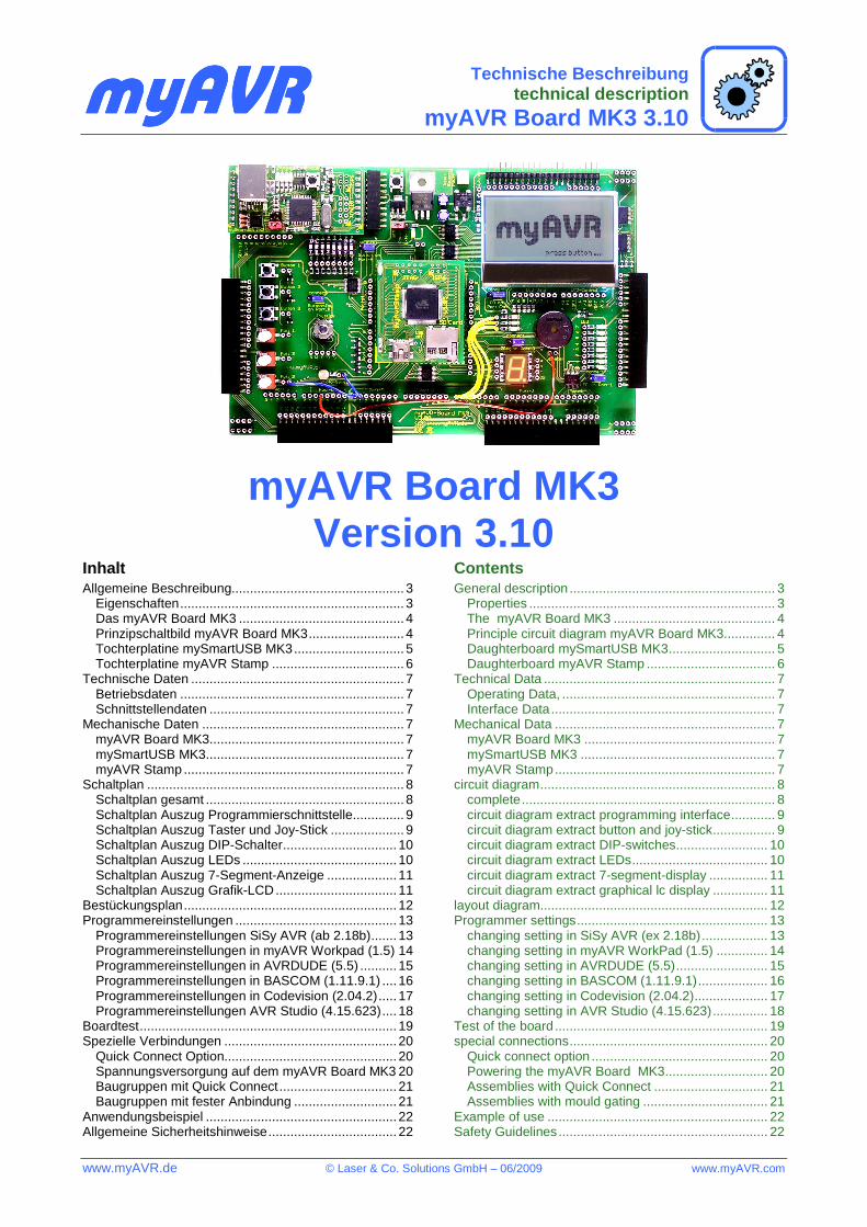
Allgemeine Beschreibung Das myAVR Board MK3 ist ein leistungsfähiges Ent-wicklungsboard für Atmel Mikrocontroller. Auf diesem Entwicklungsboard sind die Komponenten myAVR Stamp und der Programmer mySmartUSB MK3 sowie ein Grafik-display bereits integriert. Es hat zahlreiche Hardware-Komponenten und Anschlussmöglichkeiten für die Ent-wicklung und das Testen von eingebetteten Systemen. Das Board ist in SMD-Bauweise ausgeführt. Alle SMD-Bauteile sind bestückt. Das myAVR Board MK3 besitzt für alle Komponenten eine "quick connect option"; d. h. alle Geräte können per Jum-per sofort zugeschalten oder bei Bedarf frei verdrahtet werden. Des Weiteren können alle Pins einzeln miteinan-der verbunden werden. Es gibt 4 Erweiterungsports sowie eine Anschlussoption für ein myAVR Board MK1 LPT/ MK2 USB oder einen mySmartControl. Ebenso besteht die Möglichkeit zur externen Spannungsversorgung, an der ein Netzteil angeschlossen werden kann. Das Board arbeitet mit 5 V und ist kompatibel zu den bis-herigen myAVR-Produkten. Es ist mit dem leistungsstar-ken 100-PIN-ATmega (64 bis 256 KByte Programmspei-cher) mit 16 MHz, einem Mini-USB-Anschluss mit unserem bewährten CP2102 und einem microSD-Kartenhalter aus-gestattet.
General description The myAVR Board MK3 is an efficient development board for Atmel microcontrollers. On this board, the components myAVR Stamp, the programmer mySmartUSB Mk3 and a graphical display are already integrated. The board has many hardware components and also junctions to de-velop and test embedded systems. Furthermore, it is completely built in SMD and all the SMDs are already populated. For all of the pre-installed components, there are “quick connect options” to switch the specific device on or if required to wire them. In addition all of the pins can be wired among themselves. There are 4 extension ports and a connection alternative for a myAVR Board MK1 LPT / MK2 USB or rather a mySmartControl. Also there exists the way to supply the voltage with an external AC/DC adapter. The board operates with a voltage of 5 V and is compati-ble to all myAVR products up to now. It is equipped with a powerful ATmega microcontroller with 100 pins and a memory of 64 to 256 KByte at a clock frequency of 16 MHz. Further, there is a mini USB port, realized by a CP2102 multi chip and a microSD-card slot already pre-installed.
Eigenschaften • einfache Kommunikation mit dem PC oder Notebook
über die USB-Schnittstelle • Kommunikation über UART, TWI, SPI möglich • Spannungsversorgung wahlweise über USB-
Anschluss oder externe Spannungsversorgung (9-12V)
• 16 MHz Prozessor mit bis zu 256 K Byte Speicher • Industriestandard-Controller (CP2102) USB zu seriell
Konverter (mySmartUSB und myAVR Stamp PLUS) • MicroSD-Kartenhalter (myAVR Stamp PLUS) • Mini-USB-Anschluss (myAVR Stamp PLUS) • in SMD-Bauweise • Eingabegeräte: 3 Analog-Geräte, 3 Taster*, Joy-
stick*, Lichtsensor, 8 DIP-Schalter* • Ausgabegeräte: grafisches LC-Display* 64 x
128, LED-Zeile* mit 8 LEDs, Speaker, 3 LEDs, 7-Segment-Anzeige*
• updatefähig über Bootloader • Highspeed-Programmer (mySmartUSB); separat
nutzbar • Qualitätsleiterplatte FR4 gebohrt, verzinnt, Industrie-
fertigung, robust, bedruckt
Properties
• Communication between the board and the pc/notebook by USB interface
• Following protocols supported: UART, TWI, SPI • Power supply optional via USB interface or external
power supply (9-12V)
• 16 MHz processor up to 256 K Byte memory • Industry standard controller (CP2102) USB to seriell
converter (mySmartUSB and myAVR Stamp PLUS) • microSD-Slot (myAVR Stamp PLUS) • Mini-USB-connection (myAVR Stamp PLUS) • In SMD designed • Input devices: 3 analog devices, 3 buttons*, joy-
stick*, photosensor, 8 DIP- switches* • Output devices: graphical liquid crystal display* 64 x
128, LED-strip* with 8 LED, Speaker, 3 LED, seven-segment display *
• Renewable by bootloader • High speed programming (mySmartUSB), sepa-
rately useable • Quality printed circuit board FR4 pre-drilled, tin-
plated, industrial production, solid, printed
(* = mit "quick connect") (* = with “quick connect”)
Seite: 4/22 technische Beschreibung / technical description myAVR Board MK3 3.10
www.myAVR.de © Laser & Co. Solutions GmbH – 07/2009 www.myAVR.com
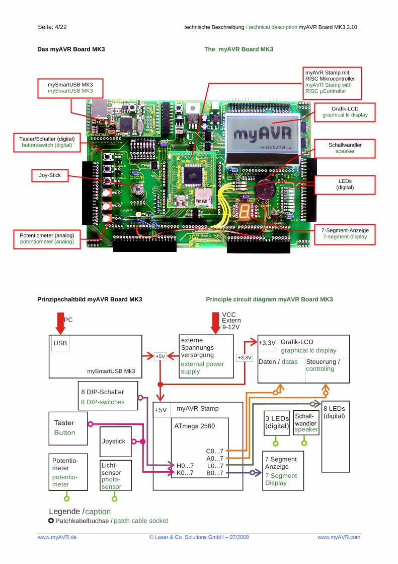
Das myAVR Board MK3
The myAVR Board MK3
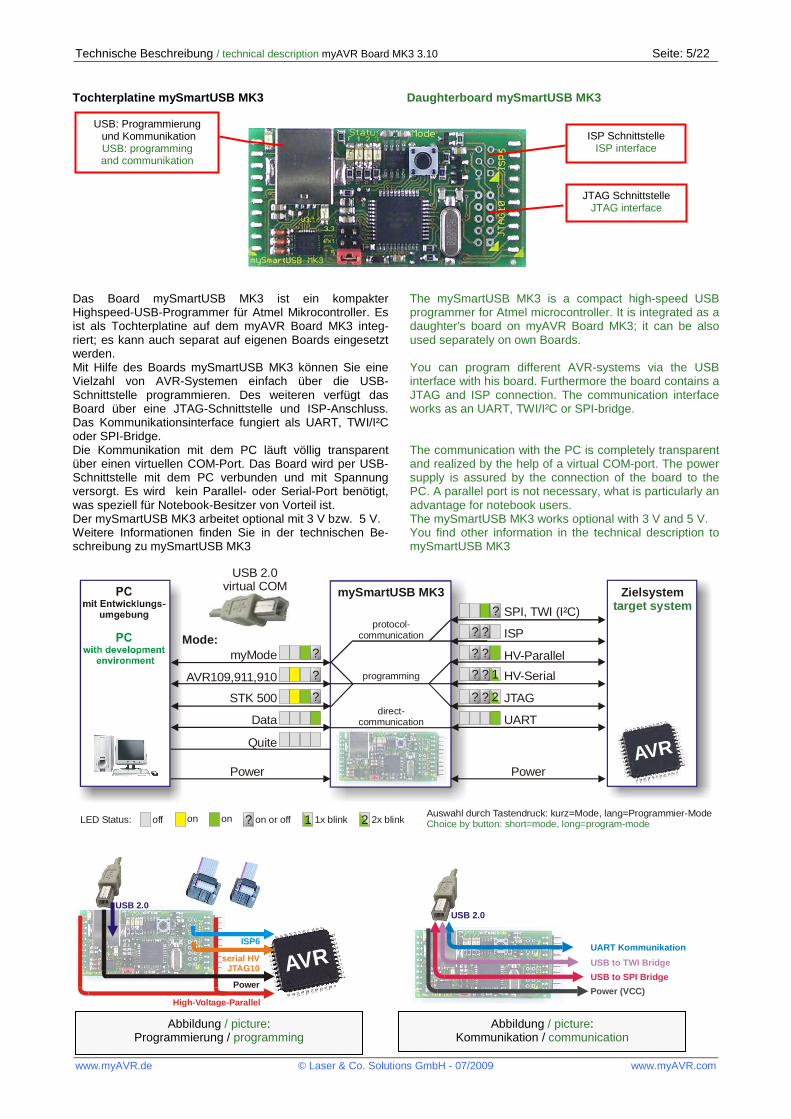
Prinzipschaltbild myAVR Board MK3
Principle circuit diagram myAVR Board MK3
8 LEDs(digital)
myAVR Stamp
K0...7 B0...7
C0...7A0...7L0...7
Joystick
mySmartUSB Mk3
USB externe Spannungs-versorgungexternal powersupply
7 SegmentAnzeige7 SegmentDisplay
Grafik-LCDgraphical lc display
Daten / Steuerung /datascontroling
+5V
+3,3V
8 DIP-Schalter
8 DIP-switches
H0...7Potentio-meterpotentio-meter
Licht-sensorphoto-sensor
VCCExtern9-12V
PC
+5V
speaker
Patchkabelbuchse / patch cable socketLegende /caption
+3,3V
mySmartUSB MK3 mySmartUSB MK3
Grafik-LCD graphical lc display
Schallwandler speaker
LEDs (digital)
7-Segment-Anzeige 7-segment-display
myAVR Stamp mit RISC Mikrocontroller myAVR Stamp with RISC µController
Taster/Schalter (digital) button/switch (digital)
Joy-Stick
Potentiometer (analog) potentiometer (analog)
Technische Beschreibung / technical description myAVR Board MK3 3.10 Seite: 5/22
www.myAVR.de © Laser & Co. Solutions GmbH - 07/2009 www.myAVR.com
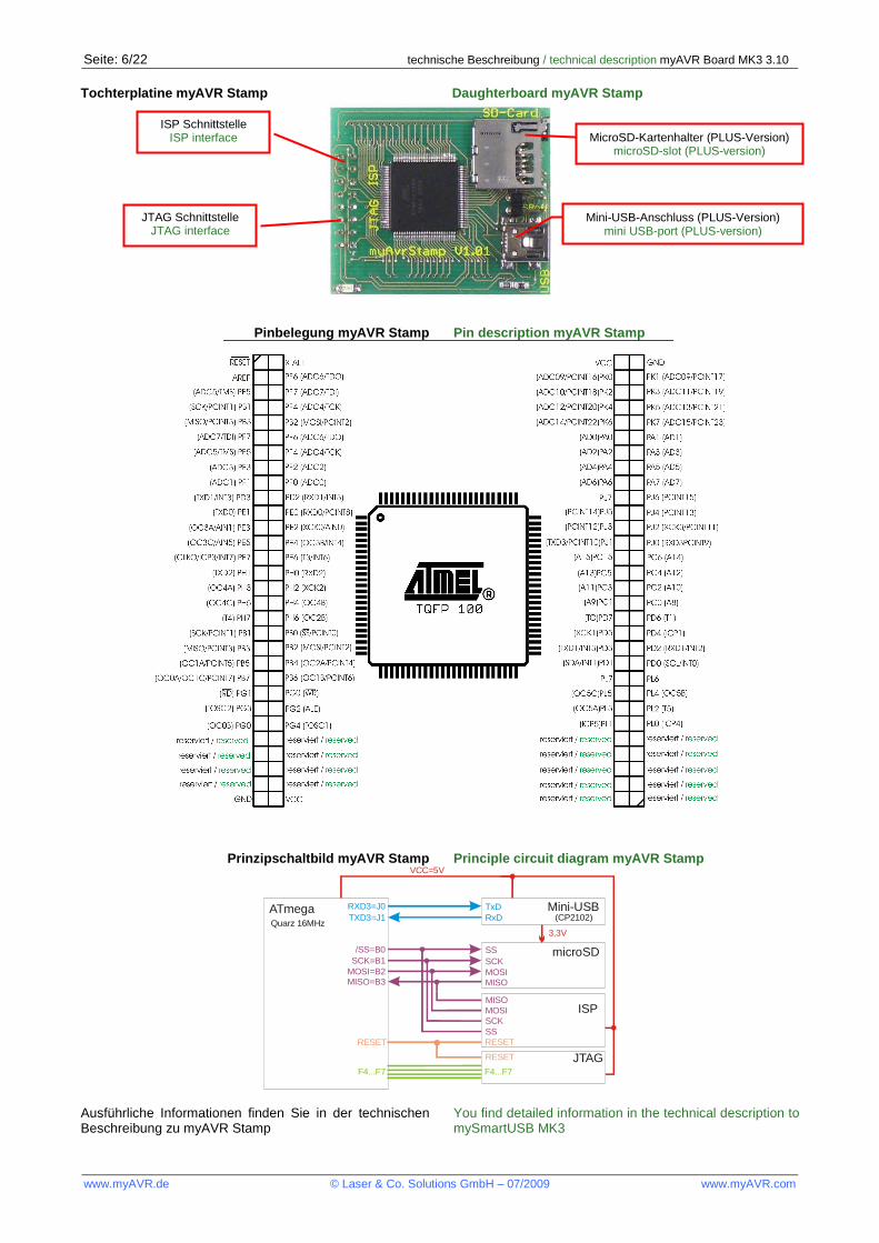
Tochterplatine mySmartUSB MK3 Daughterboard mySmartUSB MK3
Das Board mySmartUSB MK3 ist ein kompakter Highspeed-USB-Programmer für Atmel Mikrocontroller. Es ist als Tochterplatine auf dem myAVR Board MK3 integ-riert; es kann auch separat auf eigenen Boards eingesetzt werden. Mit Hilfe des Boards mySmartUSB MK3 können Sie eine Vielzahl von AVR-Systemen einfach über die USB-Schnittstelle programmieren. Des weiteren verfügt das Board über eine JTAG-Schnittstelle und ISP-Anschluss. Das Kommunikationsinterface fungiert als UART, TWI/I²C oder SPI-Bridge. Die Kommunikation mit dem PC läuft völlig transparent über einen virtuellen COM-Port. Das Board wird per USB-Schnittstelle mit dem PC verbunden und mit Spannung versorgt. Es wird kein Parallel- oder Serial-Port benötigt, was speziell für Notebook-Besitzer von Vorteil ist. Der mySmartUSB MK3 arbeitet optional mit 3 V bzw. 5 V. Weitere Informationen finden Sie in der technischen Be-schreibung zu mySmartUSB MK3
The mySmartUSB MK3 is a compact high-speed USB programmer for Atmel microcontroller. It is integrated as a daughter's board on myAVR Board MK3; it can be also used separately on own Boards. You can program different AVR-systems via the USB interface with his board. Furthermore the board contains a JTAG and ISP connection. The communication interface works as an UART, TWI/I²C or SPI-bridge. The communication with the PC is completely transparent and realized by the help of a virtual COM-port. The power supply is assured by the connection of the board to the PC. A parallel port is not necessary, what is particularly an advantage for notebook users. The mySmartUSB MK3 works optional with 3 V and 5 V. You find other information in the technical description to mySmartUSB MK3
Auswahl durch Tastendruck: kurz=Mode, lang=Programmier-ModeChoice by button: short=mode, long=program-mode? 1 2offLED Status: on on on or off 1x blink 2x blink
mySmartUSB MK3
USB 2.0virtual COM
AVR109,911,910
Power
ISP
JTAG
UART
myMode
STK 500
HV-Parallel
Zielsystemtarget system
AVR
Data
?
?
?
??
??
? 2?
HV-Serial? 1?
SPI, TWI (I²C)?
programming
protocol-communication
direct-communication
Quite
Power
Mode:
USB: Programmierung und Kommunikation USB: programming and communikation
Abbildung / picture: Programmierung / programming
Abbildung / picture: Kommunikation / communication
ISP Schnittstelle ISP interface
JTAG Schnittstelle JTAG interface
AVR
High-Voltage-Parallel
serial HVJTAG10
USB 2.0
ISP6
PowerPower (VCC)
UART Kommunikation
USB to TWI Bridge
USB to SPI Bridge
USB 2.0
Seite: 6/22 technische Beschreibung / technical description myAVR Board MK3 3.10
www.myAVR.de © Laser & Co. Solutions GmbH – 07/2009 www.myAVR.com
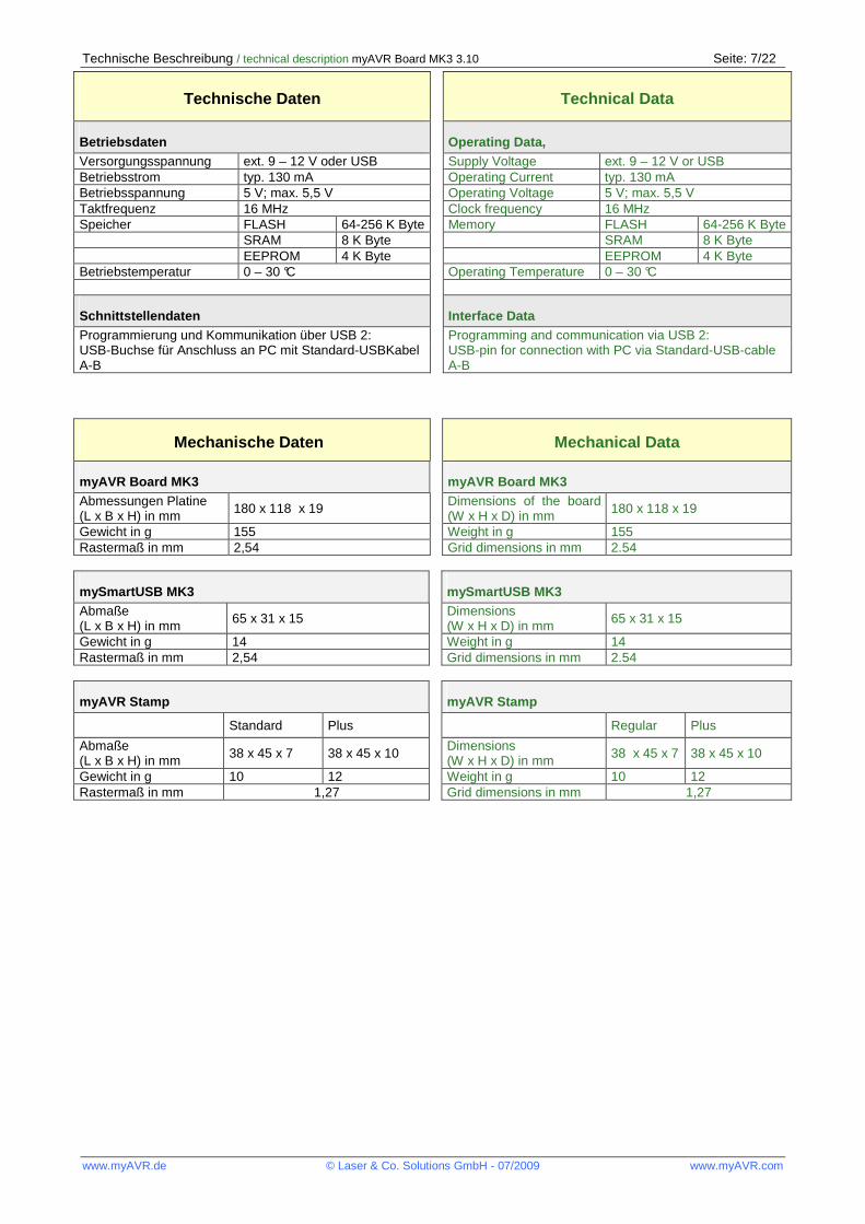
Tochterplatine myAVR Stamp
Daughterboard myAVR Stamp
Pinbelegung myAVR Stamp
Pin description myAVR Stamp
Prinzipschaltbild myAVR Stamp
Principle circuit diagram myAVR Stamp
ATmega Mini-USBRXD3=J0 TxDRxDTXD3=J1
microSD/SS=B0 SSSCK=B1 SCK
MOSI=B2 MOSIMISO=B3 MISO
VCC=5V
3,3V
(CP2102)Quarz 16MHz
F4...F7
RESET
ISP
JTAG
MISOMOSISCKSS
RESET
RESET
F4...F7
Ausführliche Informationen finden Sie in der technischen Beschreibung zu myAVR Stamp
You find detailed information in the technical description to mySmartUSB MK3
ISP Schnittstelle ISP interface
Mini-USB-Anschluss (PLUS-Version) mini USB-port (PLUS-version)
MicroSD-Kartenhalter (PLUS-Version) microSD-slot (PLUS-version)
JTAG Schnittstelle JTAG interface
Technische Beschreibung / technical description myAVR Board MK3 3.10 Seite: 7/22
www.myAVR.de © Laser & Co. Solutions GmbH - 07/2009 www.myAVR.com
Technische Daten
Technical Data
Betriebsdaten Operating Data, Versorgungsspannung ext. 9 – 12 V oder USB Supply Voltage ext. 9 – 12 V or USB Betriebsstrom typ. 130 mA Operating Current typ. 130 mA Betriebsspannung 5 V; max. 5,5 V Operating Voltage 5 V; max. 5,5 V Taktfrequenz 16 MHz Clock frequency 16 MHz Speicher FLASH 64-256 K Byte Memory FLASH 64-256 K Byte SRAM 8 K Byte SRAM 8 K Byte EEPROM 4 K Byte EEPROM 4 K Byte Betriebstemperatur 0 – 30 °C Operating Temperature 0 – 30 °C
Schnittstellendaten Interface Data Programmierung und Kommunikation über USB 2:
USB-Buchse für Anschluss an PC mit Standard-USBKabel A-B
Programming and communication via USB 2: USB-pin for connection with PC via Standard-USB-cable A-B
Mechanische Daten Mechanical Data
myAVR Board MK3
myAVR Board MK3 Abmessungen Platine (L x B x H) in mm 180 x 118 x 19 Dimensions of the board
(W x H x D) in mm 180 x 118 x 19
Gewicht in g 155 Weight in g 155 Rastermaß in mm 2,54 Grid dimensions in mm 2.54
mySmartUSB MK3
mySmartUSB MK3 Abmaße (L x B x H) in mm 65 x 31 x 15 Dimensions
(W x H x D) in mm 65 x 31 x 15
Gewicht in g 14 Weight in g 14 Rastermaß in mm 2,54 Grid dimensions in mm 2.54
myAVR Stamp
myAVR Stamp
Standard Plus Regular Plus
Abmaße (L x B x H) in mm 38 x 45 x 7 38 x 45 x 10 Dimensions
(W x H x D) in mm 38 x 45 x 7 38 x 45 x 10
Gewicht in g 10 12 Weight in g 10 12 Rastermaß in mm 1,27 Grid dimensions in mm 1,27
Seite: 8/22 technische Beschreibung / technical description myAVR Board MK3 3.10
www.myAVR.de © Laser & Co. Solutions GmbH – 07/2009 www.myAVR.com
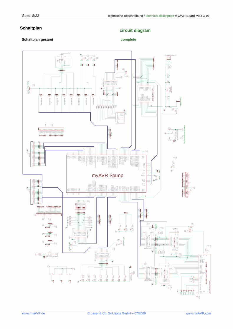
Schaltplan
circuit diagram
Schaltplan gesamt
complete
LF50 / 780
5
UA
78M
33CD
CY
R
grün
grün
grün
grün
grün
grün
grün
grün
grün
rot
gelb
grün
1K2
100k
100k
47
50k
1,8k1,8k
1,8k
1,8k
1,8k
1,8k
1,8k
1,8k
10k
10k
10k
10k
10k
10k
10k
10k
10k
1K
2
1K
2
1K
2
1K
2
1K
2
1K
2
1K
2
1K
2
1K2
1K2
1K2
F/E
E17P
74VH
CT245A
STROMSTECKER
IRLM
L6402
IRLM
L6402
IRLM
L6402
IRLM
L6402
IRLM
L6402
IRLM
L6402
IRLM
L6402
74VH
CT245A
74VHCT245A
74VHCT245A
IRLM
L6402
74VH
CT245A
PHOTO_R_VT93N1
0V
+5V
+5V+
5V
0V0
V
0V
+5V
+5V
0V
+3,3V
+5V
0V
0V
+5V
0V0V
0V+
5V
0V
+3,3V
+3,3V
+5V
+5V
+3,3V
0V
0V
0V
0V+5V
+5V
+5V
0V0V
0V
0V
+5V
0V
+5V
+5V
0V
+5V
0V0V
0V
+5V
0V
0V
0V
+5V
+5V
0V
+5V
0V
+5V
0V
+5V
0V 0V
0V+5
V0V
0V
+5V
0V
0V
+5V
0V0V
+5V
+5V
0V
+5V
0V
B2
C14
C15
C16
C17
C18
C19
C20
C21
C22
C23
C24
C25
C26
C27
C28
D2
GN
D
INO
UT
24
IN1
OU
T3
R10
R11
R12
R13
R18
R42R
43
R44
R45
R46
R47
R48
R49
3412
3412
S6
3412
S7
3412
S8
12
SG
3
123456789
1011121314151617181920
P01
P02
P03
P04
P05
P06
P07
P08
P09
P10
P11
P12
P13
P14
P15
P16
P17
P18
P19
P20
BS
1
BS
2
DATA
0D
ATA1\S
CK
DA
TA2\M
OS
ID
ATA
3\MIS
OD
ATA4
DATA
5D
ATA6
DATA
7
GN
D
OE
\TXD
PAG
EL
RE
AD
Y
RE
SE
T
VC
CW
R\R
XD
XA
0X
A1
XTA
L1
P01
P02
P03
P04
P05
P06
P07
P08
P09
P10
P11
P12
P13
P14
P15
P16
P17
P18
P19
P20
SV
9
P01P02P03P04P05P06P07P08P09P10P11P12P13P14P15P16P17P18P19P20
P01P02P03P04P05P06P07P08P09P10P11P12P13P14P15P16P17P18P19P20
1 2 3 4
123456789
10
01234567
A0
A1
A2
A3
A4
A5
A6
A7
B0
B1
B2
B3
B4
B5
B6
B7 G
ND
OE
T/R
VC
C
123456
123456
1234
123456
1 2
(A8)P
C0
(A9)P
C1
(A10)P
C2
(A11)P
C3
(A12)P
C4
(A13)P
C5
(A14)P
C6
(A15)P
C7
(AD
0)PA
0(A
D1)P
A1
(AD
2)PA
2(A
D3)P
A3
(AD
4)PA
4(A
D5)P
A5
(AD
6)PA
6(A
D7)P
A7
(AD
C0)P
F0
(AD
C1)P
F1
(AD
C2)P
F2
(AD
C3)P
F3
(AD
C4/T
CK
)PF
4(A
DC
5/TM
S)P
F5
(AD
C6/T
DO
)PF
6(A
DC
7/TD
I)PF
7
(ALE
)PG
2
(CLK
O/IC
P3/IN
T7)P
E7
(ICP
1)PD
4
(MIS
O/P
CIN
T3)PB
3(M
OS
I/PC
INT2)P
B2
(OC
0A/O
C1C
/PC
INT7)P
B7
(OC
0B)P
G5
(OC
1A/P
CIN
T5)P
B5
(OC
1B/P
CIN
T6)P
B6
(OC
2A/P
CIN
T4)P
B4
(OC
3A/A
IN1)P
E3
(OC
3B/IN
T4)P
E4
(OC
3C/IN
T5)P
E5
(RD
)PG
1
(RX
D0/P
CIN
8)PE
0
(RX
D1/IN
T2)P
D2
(SC
K/P
CIN
T1)P
B1
(SC
L/INT
0)PD
0(S
DA
/INT1)P
D1
(SS
/PC
INT
0)PB
0
(T0)P
D7
(T1)P
D6
(T3/IN
T6)P
E6
(TO
SC
1)PG
4(T
OS
C2)P
G3
(TX
D0)P
E1
(TX
D1/IN
T3)P
D3
(WR
)PG
0
(XC
K0/A
IN0)P
E2
(XC
K1)P
D5
AREF
CLK
GN
DG
ND
MISOMOSI
NC
1N
C2
NC
3N
C4
NC
5N
C6
NC
7N
C8
NC
9N
C10
NC
11N
C12
NC
13N
C14
NC
15N
C16
NC
17N
C18
PH
0(RX
D2)
PH
1(TX
D2)
PH
2(XC
K2)
PH
3(OC
4A)
PH
4(OC
4B)
PH
5(OC
4C)
PH
6(OC
2B)
PH
7(T4)
PJ0(R
XD
3/PC
INT
9)P
J1(TXD
3/PC
INT
10)P
J2(XC
K3/P
CIN
T11)
PJ3(P
CIN
T12)
PJ4(P
CIN
T13)
PJ5(P
CIN
T14)
PJ6(P
CIN
T15)
PJ7
PK
0(AD
C8/P
CIN
T16)
PK
1(AD
C9/P
CIN
T17)
PK
2(AD
C10/P
CIN
T18)
PK
3(AD
C11/P
CIN
T19)
PK
4(AD
C12/P
CIN
T20)
PK
5(AD
C13/P
CIN
T21)
PK
6(AD
C14/P
CIN
T22)
PK
7(AD
C15/P
CIN
T23)
PL0(IC
P4)
PL1(IC
P5)
PL2(T
5)P
L3(OC
5A)
PL4(O
C5B
)P
L5(OC
5C)
PL6
PL7
RESET
RXD1
SCK
TCK
TDITDOTMS
TXD1
VC
CV
CC
1 2 3 4
1234
/RD=E
/RST
/WR=R/W
AA
A0=RS
C1+C1-C2+C2-
C3+
C86=MI
CS1
DB0DB1DB2DB3DB4DB5DB6,SCLKDB7,SID
KK
P/S=PS
V-OUT
V0V1V2V3V4
VDDVSS=GND
1G
2S3
D
01234567
/OE
A0A1A2A3A4A5A6A7
B0B1B2B3B4B5B6B7
GN
D1
GN
D2
GN
D3
T/R
VC
C-A
VC
C-B
01234567
/OE
A0A1A2A3A4A5A6A7
B0B1B2B3B4B5B6B7
GN
D1
GN
D2
GN
D3
T/R
VC
C-A
VC
C-B
A10
B9
C7
COM13
COM28
D5
DP6
E4
F2
G1
1234
A0
A1
A2
A3
A4
A5
A6
A7
B0
B1
B2
B3
B4
B5
B6
B7
GN
DOE
T/R V
CC
1234
A0A1A2A3A4A5A6A7
B0B1B2B3B4B5B6B7GND
OET/RVCC
12
A0A1A2A3A4A5A6A7
B0B1B2B3B4B5B6B7GND
OET/RVCC
1 2 3 4
1234
01234567
12
A0
A1
A2
A3
A4
A5
A6
A7
B0
B1
B2
B3
B4
B5
B6
B7 G
ND
OE
T/R
VC
C
12
2-CE
NT
ER
5-GN
D
1-N
4-E
6-S
3-W
12
112
2
12
01234567
01234567
123456
0 1 2 3 4 5 6 7
12
01234567
1 2 3
12
12
12
12312
123456
123456
123456
123456
123456
1 2 3 4 5 61 2 3 4 5 61 2 3 4 5 6
123456 123456 123456
12
01234567
+
+
234567012345+-012345
PO
RT D
PO
RT B
PO
RT C
myS
martU
SB
MK
3
ON
1 2 3 4 5 6 7 8
myAVR Stamp
DisplayTech 64128K (3V
olt)
Gra
fik-LC
D 128 x 64 P
ixel
74LV
XC
3245
74LVX
C3
245
lowdrop Spannungsversorgung
RE
SE
T
CS
AR
EF
Pow
er US
B\E
xt.
Botton+Joy on P
ort K
Port-K
Port-H
Port-L
LCD
on
PO
RT A
+CLC
D C
ontrolL
CD
DATA
Port-C
Po
rt-A
LED
on Port-L
DIP
on Po
rt-H
Technische Beschreibung / technical description myAVR Board MK3 3.10 Seite: 9/22
www.myAVR.de © Laser & Co. Solutions GmbH - 07/2009 www.myAVR.com
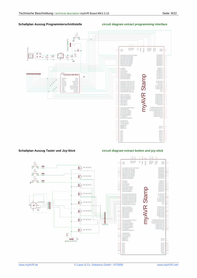
Schaltplan Auszug Programmierschnittstelle
circuit diagram extract programming interface
ST
RO
MS
TE
CK
ER
0V
0V
+5V
0V
B2 C1
C4
C5
C6
D2
GND
IN OUT
IC1
34
12
S1
BS1
BS2
DATA0DATA1\SCK
DATA2\MOSIDATA3\MISO
DATA4DATA5DATA6
DATA7
GND
OE\TXD
PAGEL
READY
RESET
VCCWR\RXD
XA0XA1
XTAL1
SV8
1 2 3 4 5 6 7 8 9 10
12
(A8)PC0(A9)PC1
(A10)PC2(A11)PC3(A12)PC4(A13)PC5(A14)PC6(A15)PC7
(AD0)PA0(AD1)PA1(AD2)PA2(AD3)PA3(AD4)PA4(AD5)PA5(AD6)PA6(AD7)PA7
(ADC0)PF0(ADC1)PF1(ADC2)PF2(ADC3)PF3(ADC4/TCK)PF4(ADC5/TMS)PF5(ADC6/TDO)PF6(ADC7/TDI)PF7
(ALE)PG2
(CLKO/ICP3/INT7)PE7
(ICP1)PD4
(MISO/PCINT3)PB3(MOSI/PCINT2)PB2
(OC0A/OC1C/PCINT7)PB7
(OC0B)PG5
(OC1A/PCINT5)PB5(OC1B/PCINT6)PB6
(OC2A/PCINT4)PB4
(OC3A/AIN1)PE3(OC3B/INT4)PE4(OC3C/INT5)PE5
(RD)PG1
(RXD0/PCIN8)PE0
(RXD1/INT2)PD2
(SCK/PCINT1)PB1
(SCL/INT0)PD0(SDA/INT1)PD1
(SS/PCINT0)PB0
(T0)PD7(T1)PD6
(T3/INT6)PE6
(TOSC1)PG4(TOSC2)PG3
(TXD0)PE1
(TXD1/INT3)PD3
(WR)PG0
(XCK0/AIN0)PE2
(XCK1)PD5
AR
EF
CLK GND
GNDMIS
OM
OS
I
NC1NC2NC3NC4NC5NC6NC7NC8
NC9NC10NC11NC12NC13NC14NC15NC16
NC17NC18
PH0(RXD2)PH1(TXD2)PH2(XCK2)PH3(OC4A)PH4(OC4B)PH5(OC4C)PH6(OC2B)
PH7(T4)
PJ0(RXD3/PCINT9)PJ1(TXD3/PCINT10)PJ2(XCK3/PCINT11)
PJ3(PCINT12)PJ4(PCINT13)PJ5(PCINT14)PJ6(PCINT15)
PJ7
PK0(ADC8/PCINT16)PK1(ADC9/PCINT17)PK2(ADC10/PCINT18)PK3(ADC11/PCINT19)PK4(ADC12/PCINT20)PK5(ADC13/PCINT21)PK6(ADC14/PCINT22)PK7(ADC15/PCINT23) PL0(ICP4)
PL1(ICP5)PL2(T5)
PL3(OC5A)PL4(OC5B)PL5(OC5C)
PL6PL7
RE
SE
T
RX
D1
SC
K
TC
K
TD
IT
DO
TM
S
TX
D1
VCCVCC
++
mySmartUSB MK3
myA
VR
Sta
mp
Pow
erU
SB
/EX
T.
Schaltplan Auszug Taster und Joy-Stick
circuit diagram extract button and joy-stick
IRLML6402
IRLML6402
IRLML6402
IRLML6402
IRLML6402
IRLML6402
IRLML6402
IRLML6402
0V
+5V
0V
0V
34
12
S4
34
12
S6
34
12
S7
(A8)PC0(A9)PC1
(A10)PC2(A11)PC3(A12)PC4(A13)PC5(A14)PC6(A15)PC7
(AD0)PA0(AD1)PA1(AD2)PA2(AD3)PA3(AD4)PA4(AD5)PA5(AD6)PA6(AD7)PA7
(ADC0)PF0(ADC1)PF1(ADC2)PF2(ADC3)PF3(ADC4/TCK)PF4(ADC5/TMS)PF5(ADC6/TDO)PF6(ADC7/TDI)PF7
(ALE)PG2
(CLKO/ICP3/INT7)PE7
(ICP1)PD4
(MISO/PCINT3)PB3(MOSI/PCINT2)PB2
(OC0A/OC1C/PCINT7)PB7
(OC0B)PG5
(OC1A/PCINT5)PB5(OC1B/PCINT6)PB6
(OC2A/PCINT4)PB4
(OC3A/AIN1)PE3(OC3B/INT4)PE4(OC3C/INT5)PE5
(RD)PG1
(RXD0/PCIN8)PE0
(RXD1/INT2)PD2
(SCK/PCINT1)PB1
(SCL/INT0)PD0(SDA/INT1)PD1
(SS/PCINT0)PB0
(T0)PD7(T1)PD6
(T3/INT6)PE6
(TOSC1)PG4(TOSC2)PG3
(TXD0)PE1
(TXD1/INT3)PD3
(WR)PG0
(XCK0/AIN0)PE2
(XCK1)PD5
AR
EF
CLK GND
GNDMIS
OM
OS
I
NC1NC2NC3NC4NC5NC6NC7NC8
NC9NC10NC11NC12NC13NC14NC15NC16
NC17NC18
PH0(RXD2)PH1(TXD2)PH2(XCK2)PH3(OC4A)PH4(OC4B)PH5(OC4C)PH6(OC2B)
PH7(T4)
PJ0(RXD3/PCINT9)PJ1(TXD3/PCINT10)PJ2(XCK3/PCINT11)
PJ3(PCINT12)PJ4(PCINT13)PJ5(PCINT14)PJ6(PCINT15)
PJ7
PK0(ADC8/PCINT16)PK1(ADC9/PCINT17)PK2(ADC10/PCINT18)PK3(ADC11/PCINT19)PK4(ADC12/PCINT20)PK5(ADC13/PCINT21)PK6(ADC14/PCINT22)PK7(ADC15/PCINT23) PL0(ICP4)
PL1(ICP5)PL2(T5)
PL3(OC5A)PL4(OC5B)PL5(OC5C)
PL6PL7
RE
SE
T
RX
D1
SC
K
TC
K
TD
IT
DO
TM
S
TX
D1
VCCVCC
1 21 2
1 2
NWC
01234567
ES
2-CENTER
5-GND
1-N
4-E
6-S
3-W
myA
VR
Sta
mp
PORT-K
Button on Port K
Seite: 10/22 technische Beschreibung / technical description myAVR Board MK3 3.10
www.myAVR.de © Laser & Co. Solutions GmbH – 07/2009 www.myAVR.com
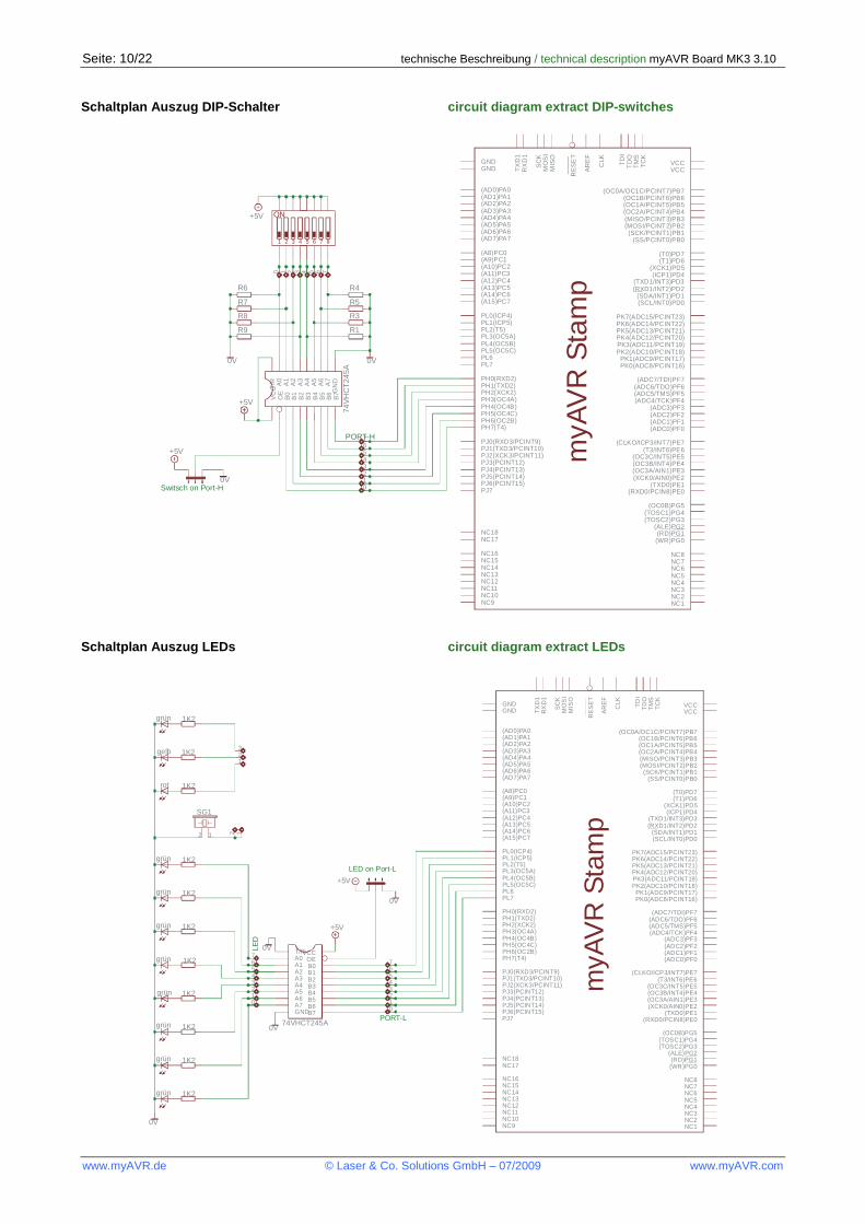
Schaltplan Auszug DIP-Schalter
circuit diagram extract DIP-switches
74V
HC
T24
5A
0V 0V
+5V
+5V
0V
+5V
R1
R3
R4
R5
R6
R7
R8
R9
(A8)PC0(A9)PC1(A10)PC2(A11)PC3(A12)PC4(A13)PC5(A14)PC6(A15)PC7
(AD0)PA0(AD1)PA1(AD2)PA2(AD3)PA3(AD4)PA4(AD5)PA5(AD6)PA6(AD7)PA7
(ADC0)PF0(ADC1)PF1(ADC2)PF2(ADC3)PF3
(ADC4/TCK)PF4(ADC5/TMS)PF5(ADC6/TDO)PF6(ADC7/TDI)PF7
(ALE)PG2
(CLKO/ICP3/INT7)PE7
(ICP1)PD4
(MISO/PCINT3)PB3(MOSI/PCINT2)PB2
(OC0A/OC1C/PCINT7)PB7
(OC0B)PG5
(OC1A/PCINT5)PB5(OC1B/PCINT6)PB6
(OC2A/PCINT4)PB4
(OC3A/AIN1)PE3(OC3B/INT4)PE4(OC3C/INT5)PE5
(RD)PG1
(RXD0/PCIN8)PE0
(RXD1/INT2)PD2
(SCK/PCINT1)PB1
(SCL/INT0)PD0(SDA/INT1)PD1
(SS/PCINT0)PB0
(T0)PD7(T1)PD6
(T3/INT6)PE6
(TOSC1)PG4(TOSC2)PG3
(TXD0)PE1
(TXD1/INT3)PD3
(WR)PG0
(XCK0/AIN0)PE2
(XCK1)PD5
AR
EF
CLKGND
GND MIS
OM
OS
I
NC1NC2NC3NC4NC5NC6NC7NC8
NC9NC10NC11NC12NC13NC14NC15NC16
NC17NC18
PH0(RXD2)PH1(TXD2)PH2(XCK2)PH3(OC4A)PH4(OC4B)PH5(OC4C)PH6(OC2B)PH7(T4)
PJ0(RXD3/PCINT9)PJ1(TXD3/PCINT10)PJ2(XCK3/PCINT11)PJ3(PCINT12)PJ4(PCINT13)PJ5(PCINT14)PJ6(PCINT15)PJ7
PK0(ADC8/PCINT16)PK1(ADC9/PCINT17)
PK2(ADC10/PCINT18)PK3(ADC11/PCINT19)PK4(ADC12/PCINT20)PK5(ADC13/PCINT21)PK6(ADC14/PCINT22)PK7(ADC15/PCINT23)PL0(ICP4)
PL1(ICP5)PL2(T5)PL3(OC5A)PL4(OC5B)PL5(OC5C)PL6PL7
RE
SE
T
RX
D1
SC
K
TC
K
TD
IT
DO
TM
S
TX
D1
VCCVCC
0 1 2 3 4 5 6 7
A0
A1
A2
A3
A4
A5
A6
A7
B0
B1
B2
B3
B4
B5
B6
B7G
ND
OE
T/R
VC
C
01234567
ON
1 2 3 4 5 6 7 8
myA
VR
Sta
mp
PORT-H
Switsch on Port-H
Schaltplan Auszug LEDs
circuit diagram extract LEDs
grün
grün
grün
grün
grün
grün
grün
grün
rot
gelb
grün
1K2
1K2
1K2
1K2
1K2
1K2
1K2
1K2
1K2
1K2
1K2
74VHCT245A
0V
+5V
0V
0V
0V
+5V
12
SG1
A0A1A2A3A4A5A6A7
B0B1B2B3B4B5B6B7GND
OET/RVCC
(A8)PC0(A9)PC1(A10)PC2(A11)PC3(A12)PC4(A13)PC5(A14)PC6(A15)PC7
(AD0)PA0(AD1)PA1(AD2)PA2(AD3)PA3(AD4)PA4(AD5)PA5(AD6)PA6(AD7)PA7
(ADC0)PF0(ADC1)PF1(ADC2)PF2(ADC3)PF3
(ADC4/TCK)PF4(ADC5/TMS)PF5(ADC6/TDO)PF6(ADC7/TDI)PF7
(ALE)PG2
(CLKO/ICP3/INT7)PE7
(ICP1)PD4
(MISO/PCINT3)PB3(MOSI/PCINT2)PB2
(OC0A/OC1C/PCINT7)PB7
(OC0B)PG5
(OC1A/PCINT5)PB5(OC1B/PCINT6)PB6
(OC2A/PCINT4)PB4
(OC3A/AIN1)PE3(OC3B/INT4)PE4(OC3C/INT5)PE5
(RD)PG1
(RXD0/PCIN8)PE0
(RXD1/INT2)PD2
(SCK/PCINT1)PB1
(SCL/INT0)PD0(SDA/INT1)PD1
(SS/PCINT0)PB0
(T0)PD7(T1)PD6
(T3/INT6)PE6
(TOSC1)PG4(TOSC2)PG3
(TXD0)PE1
(TXD1/INT3)PD3
(WR)PG0
(XCK0/AIN0)PE2
(XCK1)PD5
AR
EF
CLKGND
GND MIS
OM
OS
I
NC1NC2NC3NC4NC5NC6NC7NC8
NC9NC10NC11NC12NC13NC14NC15NC16
NC17NC18
PH0(RXD2)PH1(TXD2)PH2(XCK2)PH3(OC4A)PH4(OC4B)PH5(OC4C)PH6(OC2B)PH7(T4)
PJ0(RXD3/PCINT9)PJ1(TXD3/PCINT10)PJ2(XCK3/PCINT11)PJ3(PCINT12)PJ4(PCINT13)PJ5(PCINT14)PJ6(PCINT15)PJ7
PK0(ADC8/PCINT16)PK1(ADC9/PCINT17)
PK2(ADC10/PCINT18)PK3(ADC11/PCINT19)PK4(ADC12/PCINT20)PK5(ADC13/PCINT21)PK6(ADC14/PCINT22)PK7(ADC15/PCINT23)PL0(ICP4)
PL1(ICP5)PL2(T5)PL3(OC5A)PL4(OC5B)PL5(OC5C)PL6PL7
RE
SE
T
RX
D1
SC
K
TC
K
TD
IT
DO
TM
S
TX
D1
VCCVCC
01234567
01234567
12
123
myA
VR
Sta
mp
LED
PORT-L
LED on Port-L
Technische Beschreibung / technical description myAVR Board MK3 3.10 Seite: 11/22
www.myAVR.de © Laser & Co. Solutions GmbH - 07/2009 www.myAVR.com
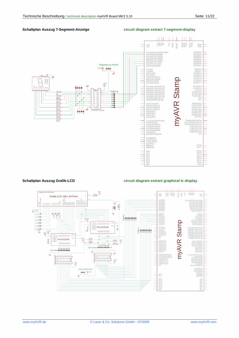
Schaltplan Auszug 7-Segment-Anzeige
circuit diagram extract 7-segment-display
74VHCT245A
0V
+5V0V
0V
0V
+5V
R2
R20
R21
R22
R23
R24
R25
R26
A1
0B
9C
7
CO
M1
3C
OM
28
D5
DP
6
E4
F2
G1
U$1
b
01234567
(A8)PC0(A9)PC1
(A10)PC2(A11)PC3(A12)PC4(A13)PC5(A14)PC6(A15)PC7
(AD0)PA0(AD1)PA1(AD2)PA2(AD3)PA3(AD4)PA4(AD5)PA5(AD6)PA6(AD7)PA7
(ADC0)PF0(ADC1)PF1(ADC2)PF2(ADC3)PF3(ADC4/TCK)PF4(ADC5/TMS)PF5(ADC6/TDO)PF6(ADC7/TDI)PF7
(ALE)PG2
(CLKO/ICP3/INT7)PE7
(ICP1)PD4
(MISO/PCINT3)PB3(MOSI/PCINT2)PB2
(OC0A/OC1C/PCINT7)PB7
(OC0B)PG5
(OC1A/PCINT5)PB5(OC1B/PCINT6)PB6
(OC2A/PCINT4)PB4
(OC3A/AIN1)PE3(OC3B/INT4)PE4(OC3C/INT5)PE5
(RD)PG1
(RXD0/PCIN8)PE0
(RXD1/INT2)PD2
(SCK/PCINT1)PB1
(SCL/INT0)PD0(SDA/INT1)PD1
(SS/PCINT0)PB0
(T0)PD7(T1)PD6
(T3/INT6)PE6
(TOSC1)PG4(TOSC2)PG3
(TXD0)PE1
(TXD1/INT3)PD3
(WR)PG0
(XCK0/AIN0)PE2
(XCK1)PD5
AR
EF
CLK GND
GNDMIS
OM
OS
I
NC1NC2NC3NC4NC5NC6NC7NC8
NC9NC10NC11NC12NC13NC14NC15NC16
NC17NC18
PH0(RXD2)PH1(TXD2)PH2(XCK2)PH3(OC4A)PH4(OC4B)PH5(OC4C)PH6(OC2B)
PH7(T4)
PJ0(RXD3/PCINT9)PJ1(TXD3/PCINT10)PJ2(XCK3/PCINT11)
PJ3(PCINT12)PJ4(PCINT13)PJ5(PCINT14)PJ6(PCINT15)
PJ7
PK0(ADC8/PCINT16)PK1(ADC9/PCINT17)PK2(ADC10/PCINT18)PK3(ADC11/PCINT19)PK4(ADC12/PCINT20)PK5(ADC13/PCINT21)PK6(ADC14/PCINT22)PK7(ADC15/PCINT23) PL0(ICP4)
PL1(ICP5)PL2(T5)
PL3(OC5A)PL4(OC5B)PL5(OC5C)
PL6PL7
RE
SE
T
RX
D1
SC
K
TC
K
TD
IT
DO
TM
S
TX
D1
VCCVCC
A0A1A2A3A4A5A6A7
B0B1B2B3B4B5B6B7GND
OET/RVCC
myA
VR
Sta
mp
7Segment on Port-B
PORT-B
cdp a
fed g
Schaltplan Auszug Grafik-LCD
circuit diagram extract graphical lc display
74V
HC
T24
5A
74V
HC
T24
5A
+5V
0V+3,3V
+3,3V
+5V
+3,3V
0V
0V
+5V
0V
0V
+5V
+5V
+5V
0V
0V0V
0V
+5V
0V
C16
C17
C18
C19
C20
C21
C22
C23
C24
R10R11
R12
R13
R18
R41
01234567
0 1 2 3 4 5 6 7
01234567
(A8)PC0(A9)PC1(A10)PC2(A11)PC3(A12)PC4(A13)PC5(A14)PC6(A15)PC7
(AD0)PA0(AD1)PA1(AD2)PA2(AD3)PA3(AD4)PA4(AD5)PA5(AD6)PA6(AD7)PA7
(ADC0)PF0(ADC1)PF1(ADC2)PF2(ADC3)PF3
(ADC4/TCK)PF4(ADC5/TMS)PF5(ADC6/TDO)PF6(ADC7/TDI)PF7
(ALE)PG2
(CLKO/ICP3/INT7)PE7
(ICP1)PD4
(MISO/PCINT3)PB3(MOSI/PCINT2)PB2
(OC0A/OC1C/PCINT7)PB7
(OC0B)PG5
(OC1A/PCINT5)PB5(OC1B/PCINT6)PB6
(OC2A/PCINT4)PB4
(OC3A/AIN1)PE3(OC3B/INT4)PE4(OC3C/INT5)PE5
(RD)PG1
(RXD0/PCIN8)PE0
(RXD1/INT2)PD2
(SCK/PCINT1)PB1
(SCL/INT0)PD0(SDA/INT1)PD1
(SS/PCINT0)PB0
(T0)PD7(T1)PD6
(T3/INT6)PE6
(TOSC1)PG4(TOSC2)PG3
(TXD0)PE1
(TXD1/INT3)PD3
(WR)PG0
(XCK0/AIN0)PE2
(XCK1)PD5
AR
EF
CLKGND
GND MIS
OM
OS
I
NC1NC2NC3NC4NC5NC6NC7NC8
NC9NC10NC11NC12NC13NC14NC15NC16
NC17NC18
PH0(RXD2)PH1(TXD2)PH2(XCK2)PH3(OC4A)PH4(OC4B)PH5(OC4C)PH6(OC2B)PH7(T4)
PJ0(RXD3/PCINT9)PJ1(TXD3/PCINT10)PJ2(XCK3/PCINT11)PJ3(PCINT12)PJ4(PCINT13)PJ5(PCINT14)PJ6(PCINT15)PJ7
PK0(ADC8/PCINT16)PK1(ADC9/PCINT17)
PK2(ADC10/PCINT18)PK3(ADC11/PCINT19)PK4(ADC12/PCINT20)PK5(ADC13/PCINT21)PK6(ADC14/PCINT22)PK7(ADC15/PCINT23)PL0(ICP4)
PL1(ICP5)PL2(T5)PL3(OC5A)PL4(OC5B)PL5(OC5C)PL6PL7
RE
SE
T
RX
D1
SC
K
TC
K
TD
IT
DO
TM
S
TXD
1
VCCVCC
/RD
=E
/RS
T
/WR
=R/W
AA
A0=
RS
C1+
C1-
C2+
C2-
C3+
C86
=MI
CS
1
DB
0D
B1
DB
2D
B3
DB
4D
B5
DB
6,S
CL
KD
B7
,SID K
K
P/S
=P
S
V-O
UT
V0
V1
V2
V3
V4
VD
DV
SS
=GN
D
/OE
A0
A1
A2
A3
A4
A5
A6
A7
B0
B1
B2
B3
B4
B5
B6
B7
GND1GND2GND3
T/R
VCC-AVCC-B
/OE
A0
A1
A2
A3
A4
A5
A6
A7
B0
B1
B2
B3
B4
B5
B6
B7
GND1GND2GND3
T/R
VCC-AVCC-B
A0
A1
A2
A3
A4
A5
A6
A7
B0
B1
B2
B3
B4
B5
B6
B7 G
ND
OE
T/R
VC
C
A0
A1
A2
A3
A4
A5
A6
A7
B0
B1
B2
B3
B4
B5
B6
B7 G
ND
OE
T/R
VC
C
myA
VR
Sta
mp
DisplayTech 64128K (3Volt)
Grafik-LCD 128 x 64 Pixel
74LVXC3245
74LVXC3245
CS
LCD DATA
LCD Control
LCD on POTZ A+C
PO
RT-
A
PO
RT
-C
Seite: 12/22 technische Beschreibung / technical description myAVR Board MK3 3.10
www.myAVR.de © Laser & Co. Solutions GmbH – 07/2009 www.myAVR.com
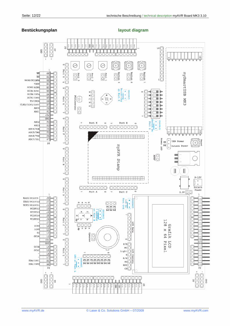
Bestückungsplan
layout diagram
Technische Beschreibung / technical description myAVR Board MK3 3.10 Seite: 13/22
www.myAVR.de © Laser & Co. Solutions GmbH - 07/2009 www.myAVR.com
Programmereinstellungen
Programmer settings
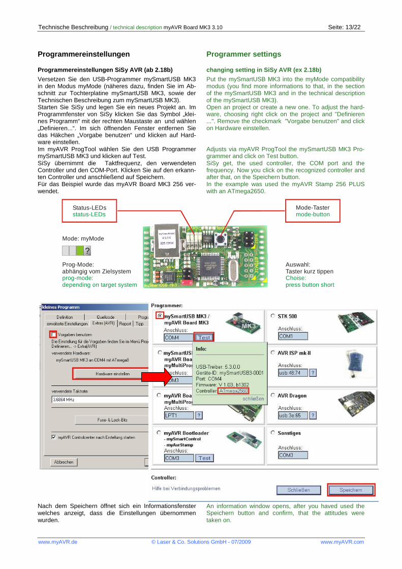
Programmereinstellungen SiSy AVR (ab 2.18b)
changing setting in SiSy AVR (ex 2.18b)
Versetzen Sie den USB-Programmer mySmartUSB MK3 in den Modus myMode (näheres dazu, finden Sie im Ab-schnitt zur Tochterplatine mySmartUSB MK3, sowie der Technischen Beschreibung zum mySmartUSB MK3). Starten Sie SiSy und legen Sie ein neues Projekt an. Im Programmfenster von SiSy klicken Sie das Symbol „klei-nes Programm“ mit der rechten Maustaste an und wählen „Definieren...“. Im sich öffnenden Fenster entfernen Sie das Häkchen „Vorgabe benutzen“ und klicken auf Hard-ware einstellen. Im myAVR ProgTool wählen Sie den USB Programmer mySmartUSB MK3 und klicken auf Test. SiSy übernimmt die Taktfrequenz, den verwendeten Controller und den COM-Port. Klicken Sie auf den erkann-ten Controller und anschließend auf Speichern. Für das Beispiel wurde das myAVR Board MK3 256 ver-wendet.
Put the mySmartUSB MK3 into the myMode compatibility modus (you find more informations to that, in the section of the mySmartUSB MK3 and in the technical description of the mySmartUSB MK3). Open an project or create a new one. To adjust the hard-ware, choosing right click on the project and "Definieren ...". Remove the checkmark "Vorgabe benutzen" and click on Hardware einstellen. Adjusts via myAVR ProgTool the mySmartUSB MK3 Pro-grammer and click on Test button. SiSy get, the used controller, the COM port and the frequency. Now you click on the recognized controller and after that, on the Speichern button. In the example was used the myAVR Stamp 256 PLUS with an ATmega2650.
?
Status-LEDsstatus-LEDs
Prog-Mode:abhängig vom Zielsystemprog-mode:depending on target system
Mode-Tastermode-button
Auswahl:Taster kurz tippenChoise:press button short
Mode: myMode
Nach dem Speichern öffnet sich ein Informationsfenster welches anzeigt, dass die Einstellungen übernommen wurden.
An information window opens, after you haved used the Speichern button and confirm, that the attitudes were taken on.
Seite: 14/22 technische Beschreibung / technical description myAVR Board MK3 3.10
www.myAVR.de © Laser & Co. Solutions GmbH – 07/2009 www.myAVR.com
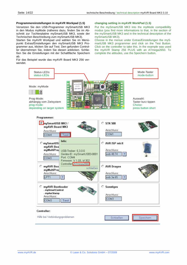
Programmereinstellungen in myAVR Workpad (1.5) changing setting in myAVR WorkPad (1.5)
Versetzen Sie den USB-Programmer mySmartUSB MK3 in den Modus myMode (näheres dazu, finden Sie im Ab-schnitt zur Tochterplatine mySmartUSB MK3, sowie der Technischen Beschreibung zum mySmartUSB MK3). Starten Sie myAVR Workpad und wählen Sie im Menü-punkt Extras/Einstellungen den mySmartUSB MK3 Pro-grammer aus, klicken Sie auf Test. Den gefunden Control-ler übernehmen Sie, indem Sie diesen anklicken. Schlie-ßen Sie die Einstellungen mit der Schaltfläche Speichern ab. Für das Beispiel wurde das myAVR Board MK3 256 ver-wendet.
Put the mySmartUSB MK3 into the myMode compatibility modus (you find more informations to that, in the section of the mySmartUSB MK3 and in the technical description of the mySmartUSB MK3). Choose in the menue under Extras/Einstellungen the myS-martUSB MK3 programmer and click on the Test Button. Click on the controller to take this. In the example was used the myAVR Stamp 256 PLUS with an ATmega2650. To complete the attitudes, use the Speichern button.
?
Status-LEDsstatus-LEDs
Prog-Mode:abhängig vom Zielsystemprog-mode:depending on target system
Mode-Tastermode-button
Auswahl:Taster kurz tippenChoise:press button short
Mode: myMode
Technische Beschreibung / technical description myAVR Board MK3 3.10 Seite: 15/22
www.myAVR.de © Laser & Co. Solutions GmbH - 07/2009 www.myAVR.com
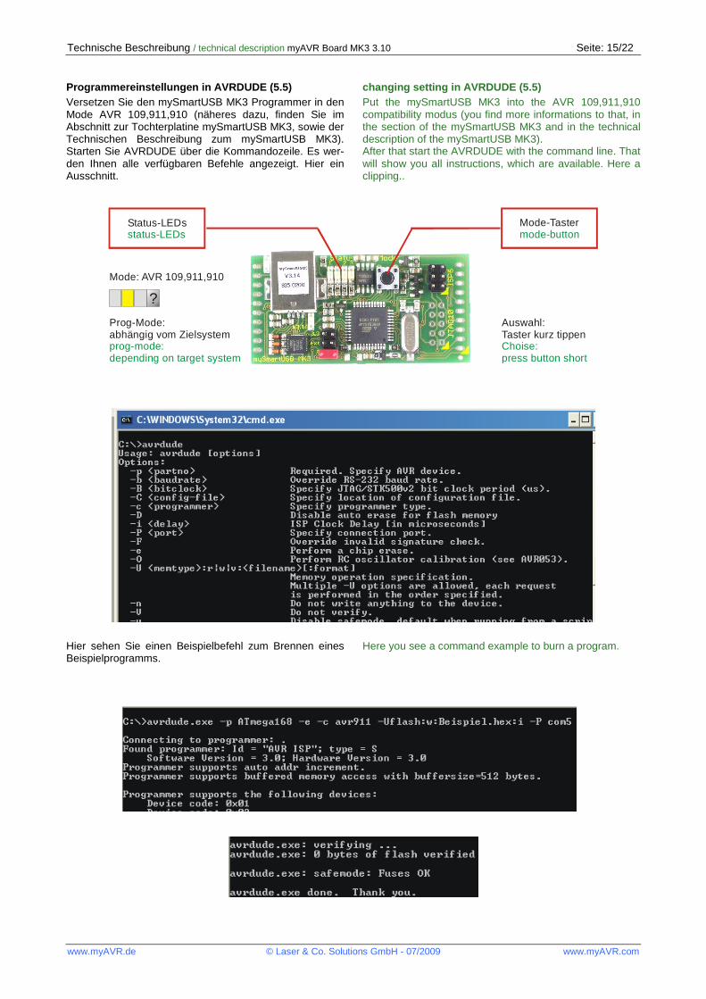
Programmereinstellungen in AVRDUDE (5.5)
changing setting in AVRDUDE (5.5) Versetzen Sie den mySmartUSB MK3 Programmer in den Mode AVR 109,911,910 (näheres dazu, finden Sie im Abschnitt zur Tochterplatine mySmartUSB MK3, sowie der Technischen Beschreibung zum mySmartUSB MK3). Starten Sie AVRDUDE über die Kommandozeile. Es wer-den Ihnen alle verfügbaren Befehle angezeigt. Hier ein Ausschnitt.
Put the mySmartUSB MK3 into the AVR 109,911,910 compatibility modus (you find more informations to that, in the section of the mySmartUSB MK3 and in the technical description of the mySmartUSB MK3). After that start the AVRDUDE with the command line. That will show you all instructions, which are available. Here a clipping..
?
Status-LEDsstatus-LEDs
Prog-Mode:abhängig vom Zielsystemprog-mode:depending on target system
Mode-Tastermode-button
Auswahl:Taster kurz tippenChoise:press button short
Mode: AVR 109,911,910
Hier sehen Sie einen Beispielbefehl zum Brennen eines Beispielprogramms.
Here you see a command example to burn a program.
Seite: 16/22 technische Beschreibung / technical description myAVR Board MK3 3.10
www.myAVR.de © Laser & Co. Solutions GmbH – 07/2009 www.myAVR.com
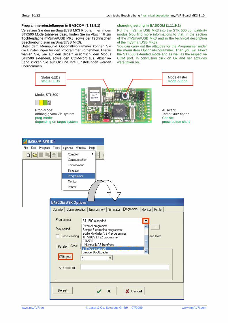
Programmereinstellungen in BASCOM (1.11.9.1)
changing setting in BASCOM (1.11.9.1) Versetzen Sie den mySmartUSB MK3 Programmer in den STK500 Mode (näheres dazu, finden Sie im Abschnitt zur Tochterplatine mySmartUSB MK3, sowie der Technischen Beschreibung zum mySmartUSB MK3). Unter dem Menüpunkt Options/Programmer können Sie die Einstellungen für den Programmer vornehmen. Hierzu wählen Sie, wie auf den Bildern ersichtlich, den Modus STK500 extended, sowie den COM-Port aus. Abschlie-ßend klicken Sie auf Ok und Ihre Einstellungen werden übernommen.
Put the mySmartUSB MK3 into the STK 500 compatibility modus (you find more informations to that, in the section of the mySmartUSB MK3 and in the technical description of the mySmartUSB MK3). You can carry out the attitudes for the Programmer under the menu item Options/Programmer. Then you will select the STK500 extended mode and as well as the respective COM port. In conclusion click on Ok and her attitudes were taken on.
?
Status-LEDsstatus-LEDs
Prog-Mode:abhängig vom Zielsystemprog-mode:depending on target system
Mode-Tastermode-button
Auswahl:Taster kurz tippenChoise:press button short
Mode: STK500
Technische Beschreibung / technical description myAVR Board MK3 3.10 Seite: 17/22
www.myAVR.de © Laser & Co. Solutions GmbH - 07/2009 www.myAVR.com
?
Status-LEDsstatus-LEDs
Prog-Mode:abhängig vom Zielsystemprog-mode:depending on target system
Mode-Tastermode-button
Auswahl:Taster kurz tippenChoise:press button short
Mode: STK500
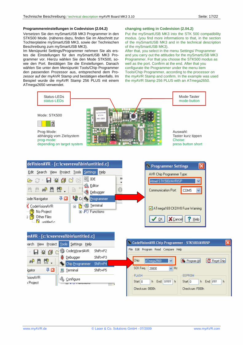
Programmereinstellungen in Codevision (2.04.2)
changing setting in Codevision (2.04.2) Versetzen Sie den mySmartUSB MK3 Programmer in den STK500 Mode. (näheres dazu, finden Sie im Abschnitt zur Tochterplatine mySmartUSB MK3, sowie der Technischen Beschreibung zum mySmartUSB MK3). Im Menüpunkt Settings/Programmer nehmen Sie als ers-tes die Einstellungen für den mySmartUSB MK3 Pro-grammer vor. Hierzu wählen Sie den Mode STK500, so-wie den Port. Bestätigen Sie die Einstellungen. Danach wählen Sie unter dem Menüpunkt Tools/Chip Programmer den passenden Prozessor aus, entsprechend dem Pro-zessor auf der myAVR Stamp und bestätigen ebenfalls. Im Beispiel wurde die myAVR Stamp 256 PLUS mit einem ATmega2650 verwendet.
Put the mySmartUSB MK3 into the STK 500 compatibility modus. (you find more informations to that, in the section of the mySmartUSB MK3 and in the technical description of the mySmartUSB MK3). After that, you select in the menu Settings/ Programmer and you carry out the attitudes for the mySmartUSB MK3 Programmer. For that you choose the STK500 modus as well as the port. Confirm at the end. After that you configurate the Programmer under the menu item Tools/Chip Programmer, according to the processor on the myAVR Stamp and confirm. In the example was used the myAVR Stamp 256 PLUS with an ATmega2650.
Seite: 18/22 technische Beschreibung / technical description myAVR Board MK3 3.10
www.myAVR.de © Laser & Co. Solutions GmbH – 07/2009 www.myAVR.com
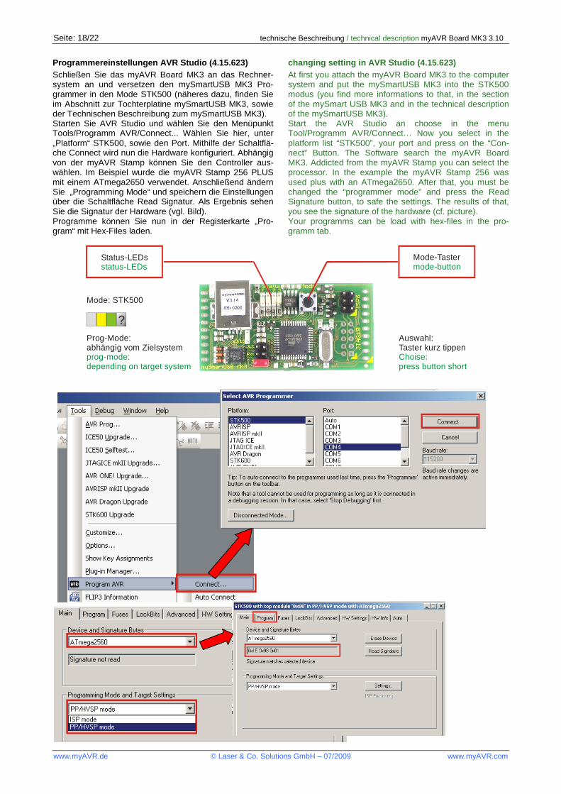
Programmereinstellungen AVR Studio (4.15.623)
changing setting in AVR Studio (4.15.623) Schließen Sie das myAVR Board MK3 an das Rechner-system an und versetzen den mySmartUSB MK3 Pro-grammer in den Mode STK500 (näheres dazu, finden Sie im Abschnitt zur Tochterplatine mySmartUSB MK3, sowie der Technischen Beschreibung zum mySmartUSB MK3). Starten Sie AVR Studio und wählen Sie den Menüpunkt Tools/Programm AVR/Connect... Wählen Sie hier, unter „Platform“ STK500, sowie den Port. Mithilfe der Schaltflä-che Connect wird nun die Hardware konfiguriert. Abhängig von der myAVR Stamp können Sie den Controller aus-wählen. Im Beispiel wurde die myAVR Stamp 256 PLUS mit einem ATmega2650 verwendet. Anschließend ändern Sie „Programming Mode“ und speichern die Einstellungen über die Schaltfläche Read Signatur. Als Ergebnis sehen Sie die Signatur der Hardware (vgl. Bild). Programme können Sie nun in der Registerkarte „Pro-gram“ mit Hex-Files laden.
At first you attach the myAVR Board MK3 to the computer system and put the mySmartUSB MK3 into the STK500 modus (you find more informations to that, in the section of the mySmart USB MK3 and in the technical description of the mySmartUSB MK3). Start the AVR Studio an choose in the menu Tool/Programm AVR/Connect… Now you select in the platform list “STK500”, your port and press on the “Con-nect” Button. The Software search the myAVR Board MK3. Addicted from the myAVR Stamp you can select the processor. In the example the myAVR Stamp 256 was used plus with an ATmega2650. After that, you must be changed the “programmer mode” and press the Read Signature button, to safe the settings. The results of that, you see the signature of the hardware (cf. picture). Your programms can be load with hex-files in the pro-gramm tab.
?
Status-LEDsstatus-LEDs
Prog-Mode:abhängig vom Zielsystemprog-mode:depending on target system
Mode-Tastermode-button
Auswahl:Taster kurz tippenChoise:press button short
Mode: STK500
Technische Beschreibung / technical description myAVR Board MK3 3.10 Seite: 19/22
www.myAVR.de © Laser & Co. Solutions GmbH - 07/2009 www.myAVR.com
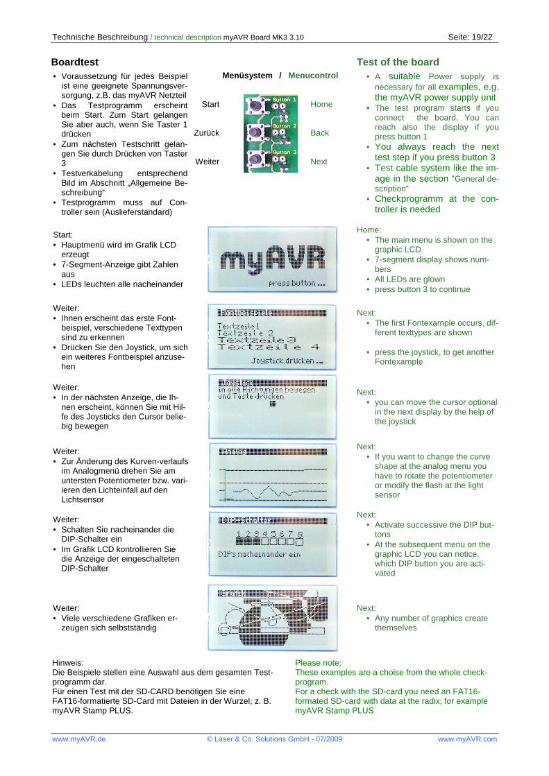
Boardtest Test of the board Menüsystem / Menucontrol • Voraussetzung für jedes Beispiel
ist eine geeignete Spannungsver-sorgung, z.B. das myAVR Netzteil
• Das Testprogramm erscheint beim Start. Zum Start gelangen Sie aber auch, wenn Sie Taster 1 drücken
• Zum nächsten Testschritt gelan-gen Sie durch Drücken von Taster 3
• Testverkabelung entsprechend Bild im Abschnitt „Allgemeine Be-schreibung“
• Testprogramm muss auf Con-troller sein (Auslieferstandard)
Start
Zurück
Weiter
Home Back Next
• A suitable Power supply is necessary for all examples, e.g. the myAVR power supply unit
• The test program starts if you connect the board. You can reach also the display if you press button 1
• You always reach the next test step if you press button 3
• Test cable system like the im-age in the section “General de-scription”
• Checkprogramm at the con-troller is needed
Start: • Hauptmenü wird im Grafik LCD
erzeugt • 7-Segment-Anzeige gibt Zahlen
aus • LEDs leuchten alle nacheinander
Home: • The main menu is shown on the
graphic LCD • 7-segment display shows num-
bers • All LEDs are glown • press button 3 to continue
Weiter: • Ihnen erscheint das erste Font-
beispiel, verschiedene Texttypen sind zu erkennen
• Drücken Sie den Joystick, um sich ein weiteres Fontbeispiel anzuse-hen
Next: • The first Fontexample occurs, dif-
ferent texttypes are shown
• press the joystick, to get another Fontexample
Weiter: • In der nächsten Anzeige, die Ih-
nen erscheint, können Sie mit Hil-fe des Joysticks den Cursor belie-big bewegen
Next: • you can move the cursor optional
in the next display by the help of the joystick
Weiter: • Zur Änderung des Kurven-verlaufs
im Analogmenü drehen Sie am untersten Potentiometer bzw. vari-ieren den Lichteinfall auf den Lichtsensor
Next: • If you want to change the curve
shape at the analog menu you have to rotate the potentiometer or modify the flash at the light sensor
Weiter: • Schalten Sie nacheinander die
DIP-Schalter ein • Im Grafik LCD kontrollieren Sie
die Anzeige der eingeschalteten DIP-Schalter
Next: • Activate successive the DIP but-
tons • At the subsequent menu on the
graphic LCD you can notice, which DIP button you are acti-vated
Weiter: • Viele verschiedene Grafiken er-
zeugen sich selbstständig
Next: • Any number of graphics create
themselves
Hinweis: Die Beispiele stellen eine Auswahl aus dem gesamten Test-programm dar. Für einen Test mit der SD-CARD benötigen Sie eine FAT16-formatierte SD-Card mit Dateien in der Wurzel; z. B. myAVR Stamp PLUS.
Please note: These examples are a choise from the whole check-program. For a check with the SD-card you need an FAT16-formated SD-card with data at the radix; for example myAVR Stamp PLUS
Seite: 20/22 technische Beschreibung / technical description myAVR Board MK3 3.10
www.myAVR.de © Laser & Co. Solutions GmbH – 07/2009 www.myAVR.com
Spezielle Verbindungen special connections
Quick Connect Option
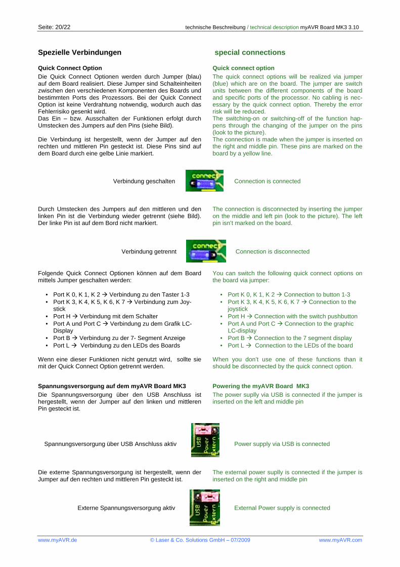
Quick connect option Die Quick Connect Optionen werden durch Jumper (blau) auf dem Board realisiert. Diese Jumper sind Schalteinheiten zwischen den verschiedenen Komponenten des Boards und bestimmten Ports des Prozessors. Bei der Quick Connect Option ist keine Verdrahtung notwendig, wodurch auch das Fehlerrisiko gesenkt wird. Das Ein – bzw. Ausschalten der Funktionen erfolgt durch Umstecken des Jumpers auf den Pins (siehe Bild). Die Verbindung ist hergestellt, wenn der Jumper auf den rechten und mittleren Pin gesteckt ist. Diese Pins sind auf dem Board durch eine gelbe Linie markiert.
The quick connect options will be realized via jumper (blue) which are on the board. The jumper are switch units between the different components of the board and specific ports of the processor. No cabling is nec-essary by the quick connect option. Thereby the error risk will be reduced. The switching-on or switching-off of the function hap-pens through the changing of the jumper on the pins (look to the picture). The connection is made when the jumper is inserted on the right and middle pin. These pins are marked on the board by a yellow line.
Verbindung geschalten
Connection is connected
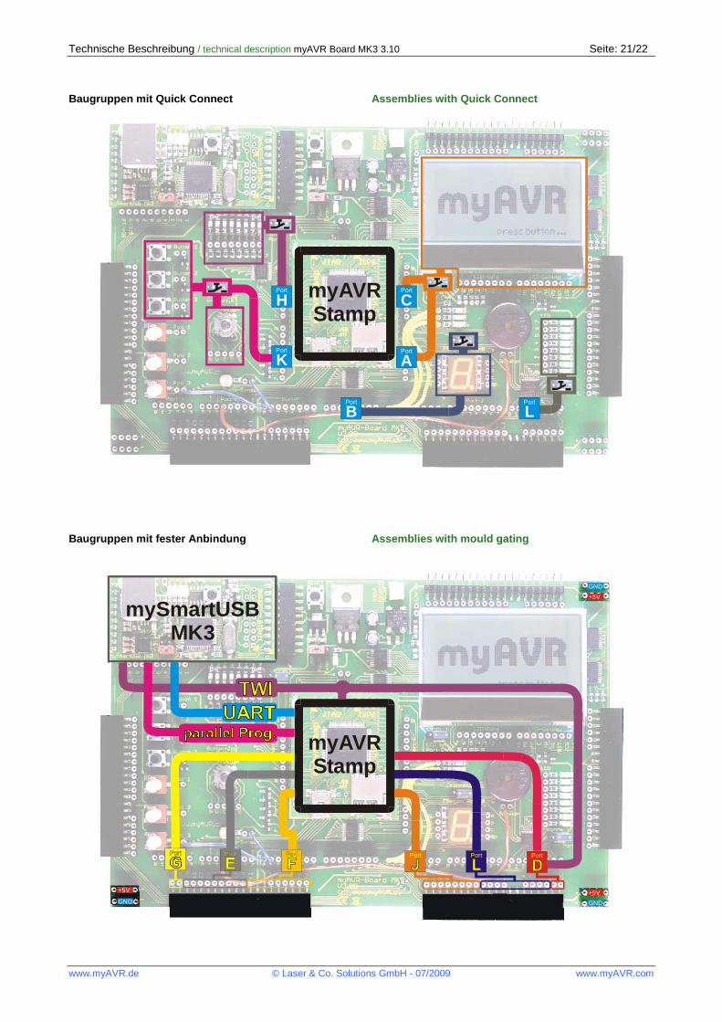
Durch Umstecken des Jumpers auf den mittleren und den linken Pin ist die Verbindung wieder getrennt (siehe Bild). Der linke Pin ist auf dem Bord nicht markiert.
The connection is disconnected by inserting the jumper on the middle and left pin (look to the picture). The left pin isn’t marked on the board.
Verbindung getrennt
Connection is disconnected
Folgende Quick Connect Optionen können auf dem Board mittels Jumper geschalten werden:
• Port K 0, K 1, K 2 � Verbindung zu den Taster 1-3 • Port K 3, K 4, K 5, K 6, K 7 � Verbindung zum Joy-
stick • Port H � Verbindung mit dem Schalter • Port A und Port C � Verbindung zu dem Grafik LC-
Display • Port B � Verbindung zu der 7- Segment Anzeige • Port L � Verbindung zu den LEDs des Boards
Wenn eine dieser Funktionen nicht genutzt wird, sollte sie mit der Quick Connect Option getrennt werden.
You can switch the following quick connect options on the board via jumper:
• Port K 0, K 1, K 2 � Connection to button 1-3 • Port K 3, K 4, K 5, K 6, K 7 � Connection to the
joystick • Port H � Connection with the switch pushbutton • Port A und Port C � Connection to the graphic
LC-display • Port B � Connection to the 7 segment display • Port L � Connection to the LEDs of the board
When you don’t use one of these functions than it should be disconnected by the quick connect option.
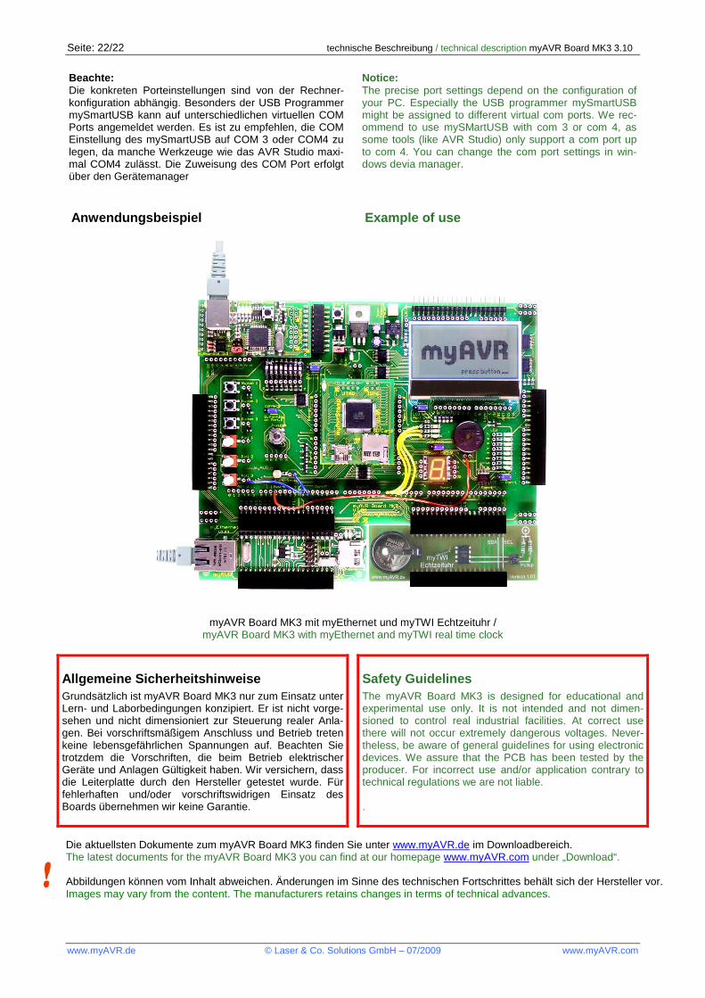
Spannungsversorgung auf dem myAVR Board MK3
Powering the myAVR Board MK3 Die Spannungsversorgung über den USB Anschluss ist hergestellt, wenn der Jumper auf den linken und mittleren Pin gesteckt ist.
The power suplly via USB is connected if the jumper is inserted on the left and middle pin
Spannungsversorgung über USB Anschluss aktiv
Power supply via USB is connected
Die externe Spannungsversorgung ist hergestellt, wenn der Jumper auf den rechten und mittleren Pin gesteckt ist.
The external power suplly is connected if the jumper is inserted on the right and middle pin
Externe Spannungsversorgung aktiv
External Power supply is connected
Technische Beschreibung / technical description myAVR Board MK3 3.10 Seite: 21/22
www.myAVR.de © Laser & Co. Solutions GmbH - 07/2009 www.myAVR.com
myAVRStamp
Port
HPort
C
Port
A
Port
BPort
L
Port
K
mySmartUSBMK3
myAVRStamp
+5V
+5V
+5VGND
GND
GND
Port PortPort
Baugruppen mit Quick Connect
Assemblies with Quick Connect
Baugruppen mit fester Anbindung
Assemblies with mould gating
Seite: 22/22 technische Beschreibung / technical description myAVR Board MK3 3.10
www.myAVR.de © Laser & Co. Solutions GmbH – 07/2009 www.myAVR.com
Beachte: Die konkreten Porteinstellungen sind von der Rechner-konfiguration abhängig. Besonders der USB Programmer mySmartUSB kann auf unterschiedlichen virtuellen COM Ports angemeldet werden. Es ist zu empfehlen, die COM Einstellung des mySmartUSB auf COM 3 oder COM4 zu legen, da manche Werkzeuge wie das AVR Studio maxi-mal COM4 zulässt. Die Zuweisung des COM Port erfolgt über den Gerätemanager
Notice: The precise port settings depend on the configuration of your PC. Especially the USB programmer mySmartUSB might be assigned to different virtual com ports. We rec-ommend to use mySMartUSB with com 3 or com 4, as some tools (like AVR Studio) only support a com port up to com 4. You can change the com port settings in win-dows devia manager.
Anwendungsbeispiel Example of use
myAVR Board MK3 mit myEthernet und myTWI Echtzeituhr / myAVR Board MK3 with myEthernet and myTWI real time clock
Allgemeine Sicherheitshinweise Grundsätzlich ist myAVR Board MK3 nur zum Einsatz unter Lern- und Laborbedingungen konzipiert. Er ist nicht vorge-sehen und nicht dimensioniert zur Steuerung realer Anla-gen. Bei vorschriftsmäßigem Anschluss und Betrieb treten keine lebensgefährlichen Spannungen auf. Beachten Sie trotzdem die Vorschriften, die beim Betrieb elektrischer Geräte und Anlagen Gültigkeit haben. Wir versichern, dass die Leiterplatte durch den Hersteller getestet wurde. Für fehlerhaften und/oder vorschriftswidrigen Einsatz des Boards übernehmen wir keine Garantie.
Safety Guidelines The myAVR Board MK3 is designed for educational and experimental use only. It is not intended and not dimen-sioned to control real industrial facilities. At correct use there will not occur extremely dangerous voltages. Never-theless, be aware of general guidelines for using electronic devices. We assure that the PCB has been tested by the producer. For incorrect use and/or application contrary to technical regulations we are not liable. .
Die aktuellsten Dokumente zum myAVR Board MK3 finden Sie unter www.myAVR.de im Downloadbereich. The latest documents for the myAVR Board MK3 you can find at our homepage www.myAVR.com under „Download“. Abbildungen können vom Inhalt abweichen. Änderungen im Sinne des technischen Fortschrittes behält sich der Hersteller vor. Images may vary from the content. The manufacturers retains changes in terms of technical advances.


![Statistik-Telegramm 2012/2013 [pdf-Datei: 400 kByte]](https://img.pdfslide.org/doc/110x75/5867c1901a28abd1568b903e/statistik-telegramm-20122013-pdf-datei-400-kbyte.jpg)