Embed Size (px)
Citation preview
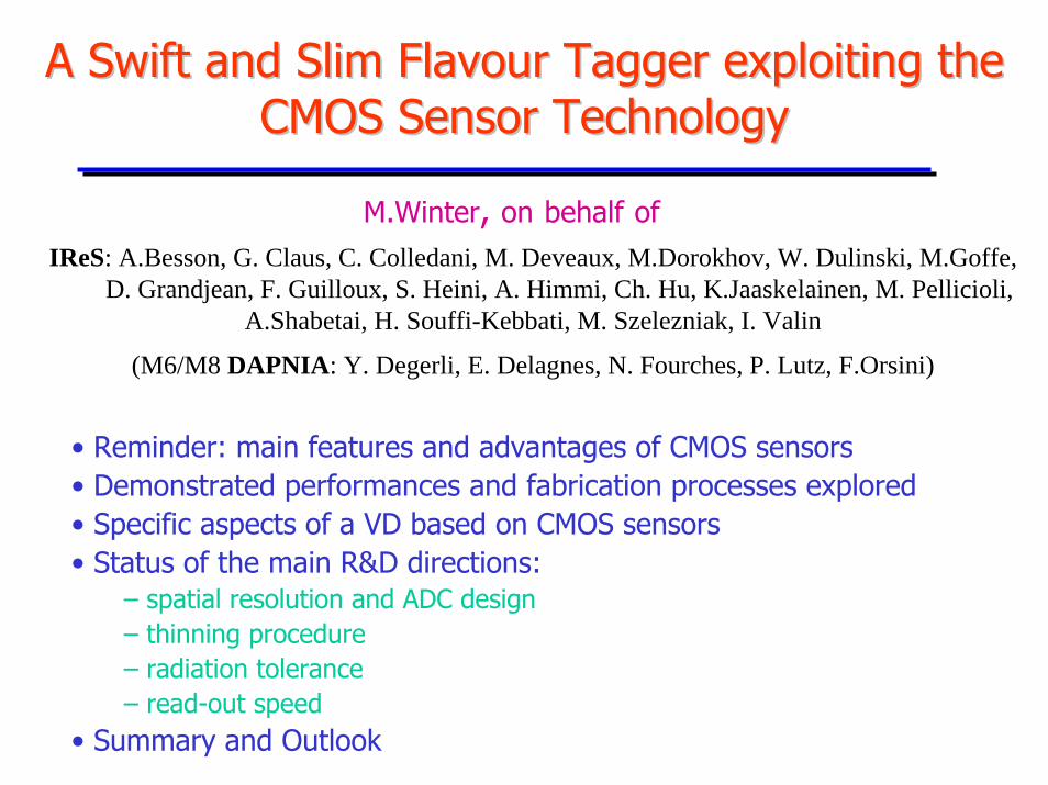
A Swift and Slim A Swift and Slim FlavourFlavour TaggerTagger exploiting the exploiting the CMOS Sensor TechnologyCMOS Sensor Technology
M.Winter, on behalf ofIReS: A.Besson, G. Claus, C. Colledani, M. Deveaux, M.Dorokhov, W. Dulinski, M.Goffe,
D. Grandjean, F. Guilloux, S. Heini, A. Himmi, Ch. Hu, K.Jaaskelainen, M. Pellicioli, A.Shabetai, H. Souffi-Kebbati, M. Szelezniak, I. Valin
(M6/M8 DAPNIA: Y. Degerli, E. Delagnes, N. Fourches, P. Lutz, F.Orsini)
• Reminder: main features and advantages of CMOS sensors • Demonstrated performances and fabrication processes explored• Specific aspects of a VD based on CMOS sensors• Status of the main R&D directions:
– spatial resolution and ADC design– thinning procedure – radiation tolerance – read-out speed
• Summary and Outlook
LCWS-05, SLAC, March 2005 CMOS Strasbourg - Saclay 2
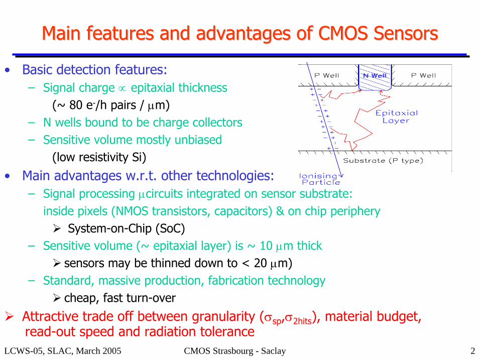
Main features and advantages of CMOS SensorsMain features and advantages of CMOS Sensors
• Basic detection features:– Signal charge ∝ epitaxial thickness
(~ 80 e-/h pairs / µm)– N wells bound to be charge collectors– Sensitive volume mostly unbiased
(low resistivity Si)
• Main advantages w.r.t. other technologies:– Signal processing µcircuits integrated on sensor substrate:
inside pixels (NMOS transistors, capacitors) & on chip peripherySystem-on-Chip (SoC)
– Sensitive volume (~ epitaxial layer) is ~ 10 µm thick sensors may be thinned down to < 20 µm)
– Standard, massive production, fabrication technologycheap, fast turn-over
Attractive trade off between granularity (σsp,σ2hits), material budget,read-out speed and radiation tolerance
3
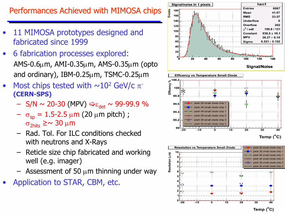
Performances Achieved with MIMOSA chipsPerformances Achieved with MIMOSA chips
• 11 MIMOSA prototypes designed and fabricated since 1999
• 6 fabrication processes explored: AMS-0.6µm, AMI-0.35µm, AMS-0.35µm (optoand ordinary), IBM-0.25µm, TSMC-0.25µm
• Most chips tested with ~102 GeV/c π-
(CERN-SPS)– S/N ~ 20-30 (MPV) εdet ~ 99-99.9 %– σsp = 1.5-2.5 µm (20 µm pitch) ;
σ2hits ≥~ 30 µm– Rad. Tol. For ILC conditions checked
with neutrons and X-Rays– Reticle size chip fabricated and working
well (e.g. imager)– Assessment of 50 µm thinning under way
• Application to STAR, CBM, etc.
LCWS-05, SLAC, March 2005 CMOS Strasbourg - Saclay 4
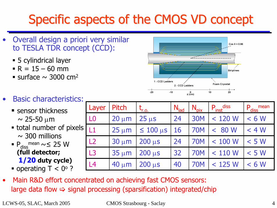
Specific aspects of the CMOS VD conceptSpecific aspects of the CMOS VD concept• Overall design a priori very similar
to TESLA TDR concept (CCD):
• Basic characteristics:
• Main R&D effort concentrated on achieving fast CMOS sensors:large data flow signal processing (sparsification) integrated/chip
5 cylindrical layerR = 15 – 60 mmsurface ~ 3000 cm2
Layer Pitch tr.o. Nlad Npix Pinstdiss Pdiss
mean
L0 20 µm 25 µs 24 30M < 120 W < 6 W
L1 25 µm ≤ 100 µs 16 70M < 80 W < 4 W
L2 30 µm 200 µs 24 70M < 100 W < 5 W
L3 35 µm 200 µs 32 70M < 110 W < 5 W
L4 40 µm 200 µs 40 70M < 125 W < 6 W
sensor thickness ~ 25-50 µmtotal number of pixels~ 300 millionsPdiss
mean ~≤ 25 W (full detector; 1/20 duty cycle)operating T < 0o ?
LCWS-05, SLAC, March 2005 CMOS Strasbourg - Saclay 5
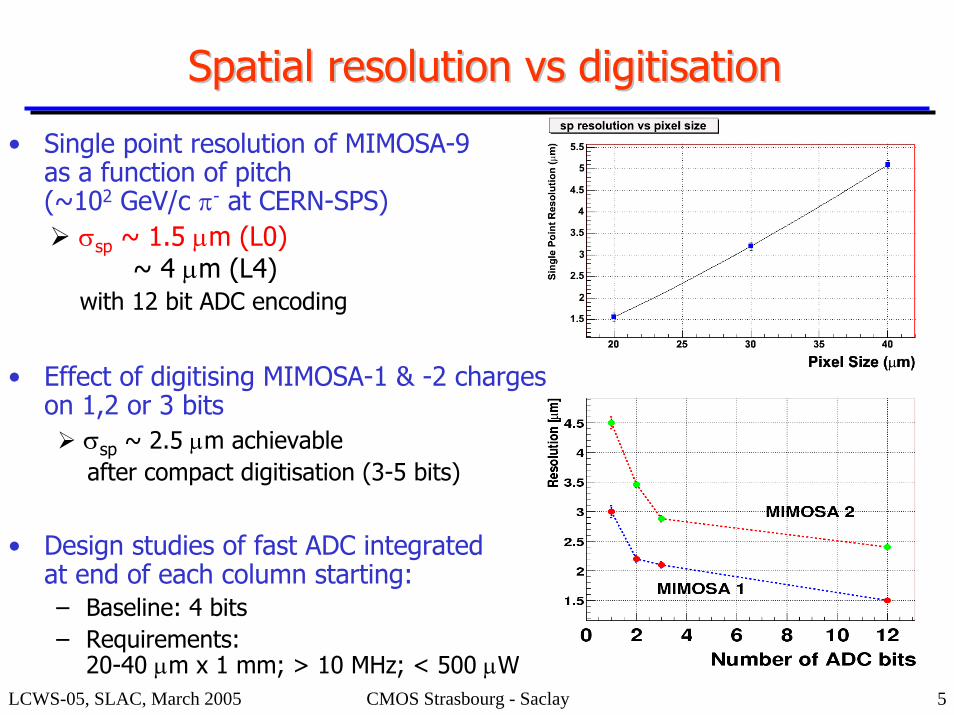
Spatial resolution Spatial resolution vsvs digitisationdigitisation
• Single point resolution of MIMOSA-9 as a function of pitch (~102 GeV/c π- at CERN-SPS)
• Effect of digitising MIMOSA-1 & -2 charges on 1,2 or 3 bits
• Design studies of fast ADC integrated at end of each column starting:– Baseline: 4 bits– Requirements:
20-40 µm x 1 mm; > 10 MHz; < 500 µW
σsp ~ 1.5 µm (L0)~ 4 µm (L4)
with 12 bit ADC encoding
σsp ~ 2.5 µm achievableafter compact digitisation (3-5 bits)
LCWS-05, SLAC, March 2005 CMOS Strasbourg - Saclay 6
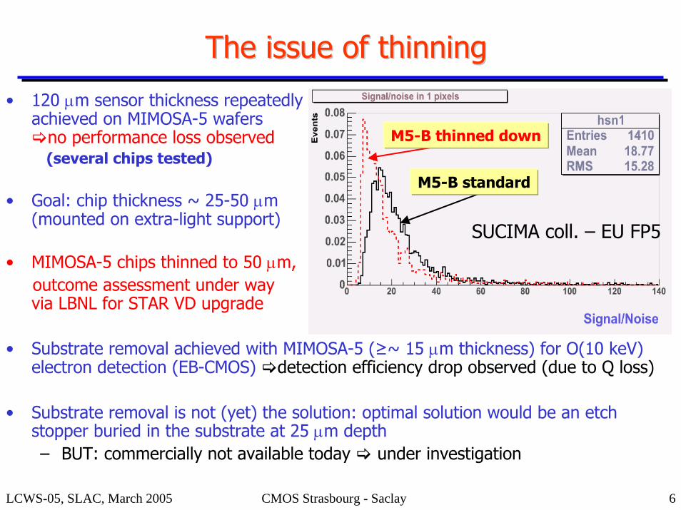
The issue of thinningThe issue of thinning
• 120 µm sensor thickness repeatedly achieved on MIMOSA-5 wafers
no performance loss observed
(several chips tested)
• Goal: chip thickness ~ 25-50 µm (mounted on extra-light support)
• MIMOSA-5 chips thinned to 50 µm, outcome assessment under way via LBNL for STAR VD upgrade
• Substrate removal achieved with MIMOSA-5 (≥~ 15 µm thickness) for O(10 keV) electron detection (EB-CMOS) detection efficiency drop observed (due to Q loss)
• Substrate removal is not (yet) the solution: optimal solution would be an etch stopper buried in the substrate at 25 µm depth– BUT: commercially not available today under investigation
M5-B standard
M5-B thinned down
SUCIMA coll. – EU FP5
LCWS-05, SLAC, March 2005 CMOS Strasbourg - Saclay 7
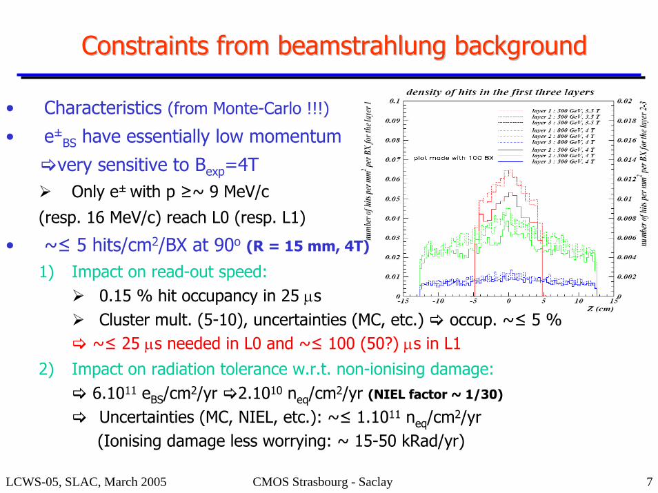
Constraints from Constraints from beamstrahlungbeamstrahlung backgroundbackground
• Characteristics (from Monte-Carlo !!!)
• e±BS have essentially low momentum
very sensitive to Bexp=4TOnly e± with p ≥~ 9 MeV/c
(resp. 16 MeV/c) reach L0 (resp. L1)
• ~≤ 5 hits/cm2/BX at 90o (R = 15 mm, 4T)
1) Impact on read-out speed:0.15 % hit occupancy in 25 µsCluster mult. (5-10), uncertainties (MC, etc.) occup. ~≤ 5 %
~≤ 25 µs needed in L0 and ~≤ 100 (50?) µs in L12) Impact on radiation tolerance w.r.t. non-ionising damage:
6.1011 eBS/cm2/yr 2.1010 neq/cm2/yr (NIEL factor ~ 1/30)
Uncertainties (MC, NIEL, etc.): ~≤ 1.1011 neq/cm2/yr(Ionising damage less worrying: ~ 15-50 kRad/yr)
LCWS-05, SLAC, March 2005 CMOS Strasbourg - Saclay 8
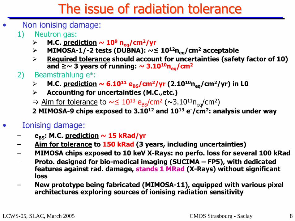
The issue of radiation toleranceThe issue of radiation tolerance• Non ionising damage:
1) Neutron gas:M.C. prediction ~ 109 neq/cm2/yrMIMOSA-1/-2 tests (DUBNA): ~≤ 1012neq/cm2 acceptableRequired tolerance should account for uncertainties (safety factor of 10) and ≥~ 3 years of running: ~ 3.1010neq/cm2
2) Beamstrahlung e±:M.C. prediction ~ 6.1011 eBS/cm2/yr (2.1010neq/cm2/yr) in L0Accounting for uncertainties (M.C.,etc.)
Aim for tolerance to ~≤ 1013 eBS/cm2 (~3.1011neq/cm2)2 MIMOSA-9 chips exposed to 3.1012 and 1013 e-/cm2: analysis under way
• Ionising damage:– eBS: M.C. prediction ~ 15 kRad/yr– Aim for tolerance to 150 kRad (3 years, including uncertainties)– MIMOSA chips exposed to 10 keV X-Rays: no perfo. loss for several 100 kRad– Proto. designed for bio-medical imaging (SUCIMA – FP5), with dedicated
features against rad. damage, stands 1 MRad (X-Rays) without significant loss
– New prototype being fabricated (MIMOSA-11), equipped with various pixel architectures exploring sources of ionising radiation sensitivity
LCWS-05, SLAC, March 2005 CMOS Strasbourg - Saclay 9
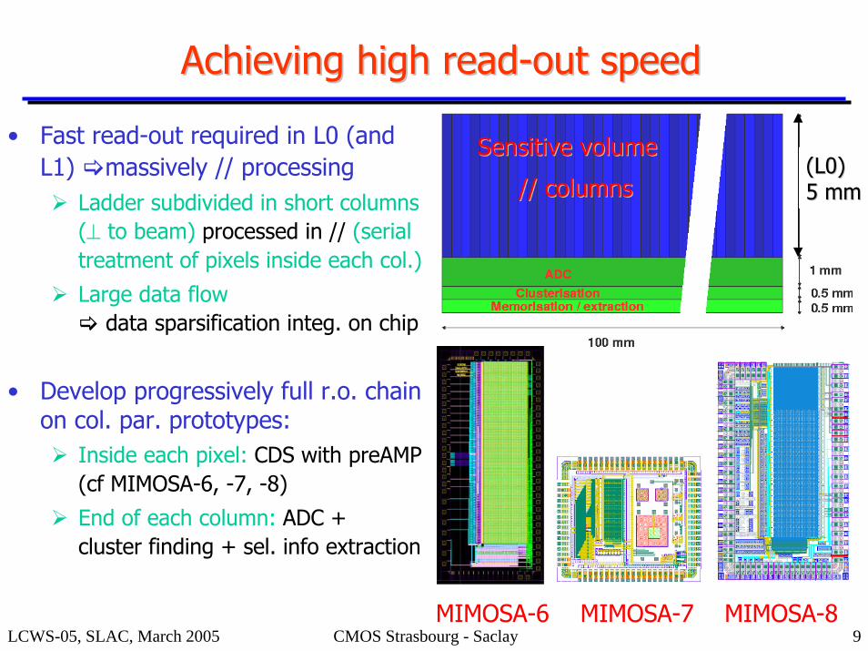
Achieving high readAchieving high read--out speedout speed
• Fast read-out required in L0 (and L1) massively // processing
Ladder subdivided in short columns (⊥ to beam) processed in // (serial treatment of pixels inside each col.)
Large data flow data sparsification integ. on chip
• Develop progressively full r.o. chain on col. par. prototypes:
Inside each pixel: CDS with preAMP(cf MIMOSA-6, -7, -8)
End of each column: ADC + cluster finding + sel. info extraction
// columns// columns(L0)(L0)5 mm5 mm
Sensitive volumeSensitive volume
MIMOSA-6 MIMOSA-7 MIMOSA-8
LCWS-05, SLAC, March 2005 CMOS Strasbourg - Saclay 10
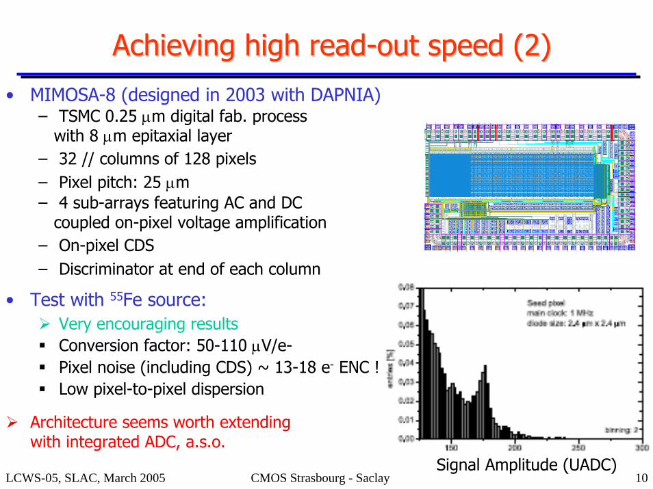
Achieving high readAchieving high read--out speed (2)out speed (2)
• MIMOSA-8 (designed in 2003 with DAPNIA)– TSMC 0.25 µm digital fab. process
with 8 µm epitaxial layer– 32 // columns of 128 pixels– Pixel pitch: 25 µm – 4 sub-arrays featuring AC and DC
coupled on-pixel voltage amplification– On-pixel CDS– Discriminator at end of each column
• Test with 55Fe source:Very encouraging resultsConversion factor: 50-110 µV/e-Pixel noise (including CDS) ~ 13-18 e- ENC !Low pixel-to-pixel dispersion
Architecture seems worth extending with integrated ADC, a.s.o.
Signal Amplitude (UADC)
LCWS-05, SLAC, March 2005 CMOS Strasbourg - Saclay 11
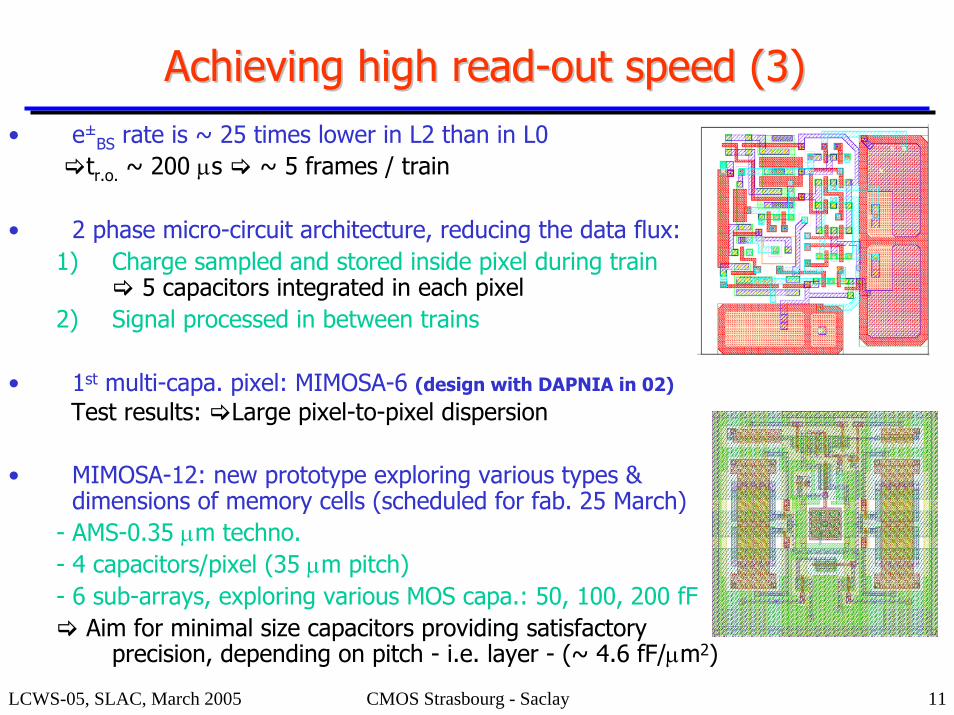
Achieving high readAchieving high read--out speed (3)out speed (3)• e±
BS rate is ~ 25 times lower in L2 than in L0tr.o. ~ 200 µs ~ 5 frames / train
• 2 phase micro-circuit architecture, reducing the data flux:1) Charge sampled and stored inside pixel during train
5 capacitors integrated in each pixel2) Signal processed in between trains
• 1st multi-capa. pixel: MIMOSA-6 (design with DAPNIA in 02)Test results: Large pixel-to-pixel dispersion
• MIMOSA-12: new prototype exploring various types & dimensions of memory cells (scheduled for fab. 25 March)
- AMS-0.35 µm techno.- 4 capacitors/pixel (35 µm pitch)- 6 sub-arrays, exploring various MOS capa.: 50, 100, 200 fF
Aim for minimal size capacitors providing satisfactory precision, depending on pitch - i.e. layer - (~ 4.6 fF/µm2)
MIMOSA-6
LCWS-05, SLAC, March 2005 CMOS Strasbourg - Saclay 12
Summary and OutlookSummary and Outlook
• Concept of vertex detector using features of CMOS sensors progressing, based on requirements accounting for uncertainties (eBS !)
• Well established performances:– S/N, εdet, σsp– Rad. Tolerance to neutrons and X-Rays– 120 µm thinning of Megapixel sensors
• Most recent achievements– Fast col. // pixel architecture (integrated CDS) found, with low noise
(< 20 e- ENC) and small pixel-to-pixel dispersion– Assessment of a well performing R&D fabrication process:
AMS-035 µm (opto and epi-free) very good perfo. even with 40 µm pitch (L4)– Checks of tolerance to 10-20 MeV electrons under way– Outcome of thinning to 50 µm under study (≥~ 15 µm not yet OK)
• Next important steps:1) Fast column // sensor with digital output, adapted to L0-1
(integrated low power, fast and compact 4-bit ADC)2) New multi-memory cell sensor adapted to L2-4– Complete study of MIMOSA-5 thinning to ~ 50 µm with LBL– Investigate characteristics of new fab. processes (e.g. IBM-0.13 µm, UMC-0.18 µm)
Thinning no-epi sensors is very appealing: any possibility ?Privileged contact with a foundry would be very valuable…
Aim for a fast col. // megapixel proto providing digital output in 2007