Embed Size (px)
Citation preview
Höchstfrequenztechnik und Quantenelektronik
On-wafer Characterization of MM-wave and THz
Circuits Using Electrooptic Sampling
Mehran Jamshidifar

On-Wafer Characterization of MM-Wave
and THz Circuits Using Electrooptic
Sampling
Von der Naturwissenschaflich-Technischen Fakultät der
Universität Siegen
zur Erlangung das akademischen Grades
Doktor der Ingenieurwissenschaften
(Dr.-Ing.)
genehmigte
DISSERTATION
vorgelegt von
M.Sc. Mehran Jamshidifar
aus Khorram Abad
1. Gutachter: Prof. Dr.-Ing. Peter Haring-Bolívar
2. Gutachter: Prof. Dr.-Ing. Jörn Schmedt auf der Günne
Vorsitzender: Prof. Dr.-Ing. Joachim Ender
Tag der mündlichen Prüfung: 04. Oktober 2016
Band 7 aus der Schriftenreihe
Höchstfrequenztechnik und Quantenelektronik
Prof. Dr.-Ing. Peter Haring Bolívar
Naturwissenschaftlich-Technische Fakultät
Universität Siegen
57068 Siegen
urn:nbn:de:hbz:467-10849
Gedruckt auf alterungsbeständigem holz- und säurefreiem Papier

To the memory of my father,
To my beloved mother and wife

I
Abstract
THz, the electromagnetic spectrum lying between millimeter waves and optics, is
nowadays widely utilized in the applications such as material inspection, medicine,
explosives detection and astronomy. Although optical and photonic based systems
for generating THz waves can fully cover the upper band of the THz spectrum (from
several THz to far infrared), they are inefficient at lower frequency bands i.e., mm-
waves, and at the same time inappropriately bulky for portable applications. In
contrast, recent progress in solid states electronics in conjunction with aggressive
scaling of devices are promising to facilitate the future availability of THz systems
realized as compact and cheap all-electronic solutions. THz microelectronics is an
increasingly relevant field of activities, therefore.
Without concerning about the challenges in the design and fabrication of such
devices, their performance needs to be characterized with systems faster than the
device itself; therefore, we face with limitations. Recently, the measurement
bandwidth of microwave network analyzers equipped with extension modules has
extended beyond 1 THz. However, their calibration is a challenging task and
performing a full band measurement, due to a need for waveguide components,
considerably increases the cost and time of measurement. Systematic errors in system
calibration due to lack of precise models for devices at THz frequencies are also
remarkable drawbacks of this approach. An eligible alternative for these systems is
the use of electrooptic and photoconductive sampling which rely on optical and
photonic approaches. These techniques with the help of femtosecond pulse lasers
provide a very broadband measurement system far beyond today’s electronic devices
bandwidth without suffering from the challenges of the electronic approach. In
particular electrooptic sampling with non-contact probing can also perform useful
high resolution near field scanning of devices.
The aim of this thesis is to demonstrate the electrooptic sampling for the
characterization of mm-wave and THz electronic devices. To this end, an extremely
broadband (microwave to THz) device, which is a 65-nm CMOS nonlinear
transmission line (NLTL), is used as the device under test. Before showing the
measurement results for this device, the advances in THz electronics as well as their
common the characterization techniques are reviewed. For the characterization, a
rather compact EOS experimental setup featured with a large dynamic range, high
sensitivity and high spatial resolution is presented. In the measurement phase, it is
shown that what challenges in particular for the characterization of a nonlinear
device we may face to and which scenarios can be used to overcome them. The
relative jitter in EOS, known as the most prohibiting factor for achieving a high
measurement bandwidth, is resolved with a novel synchronization technique called
Laser Master Laser Slave (LM-LS). This is achieved by feeding the DUT with a
microwave signal which is generated from the comb harmonics of the femtosecond
II
laser. Since the signal is sampled by the laser itself, EOS provides a fully coherent
heterodyne detection which helps to significantly increase the detection bandwidth
of the system from 50 GHz up to 300 GHz which is presently restricted by the DUT
fabrication technology i.e. the 65-nm CMOS. Furthermore, it is shown that for
nonlinear devices, measurement with EOS can outperform traditional microwave
network analyzer measurements and in particular it can detect hidden features like
conversion losses which may not be observed by electronic techniques. In the end by
performing photoconductive measurements for the DUT, a good comparison
between electrooptic and photoconductive sampling in terms of their detection
bandwidth and image resolution is demonstrated.
III
Zusammenfassung
THz, das elektromagnetische Spektrum, das zwischen Millimeterwellen und Optik
liegt, ist weit verbreitet in Anwendungsgebieten wie Materialinspektion, Medizin,
Entdeckung von Sprengstoffen und Astronomie. Obwohl auf Optik und Photonik
basierende Systeme für Generation von Terahertz-wellen die oberen Bandbreit des
THz-Spektrums vollig abdecken koennen, sind sie ineffizient in den unteren
Frequenzbändern, wie etwa dem mm-Wellenbereich, und gleichzeitig sind ihre
Größen ungeeignet für tragbare Anwendungen. Im Gegensatz dazu versprechen die
aktuellen Fortschritte in der Festkörper Elektronik in Verbindung mit einer
aggressiven Skalierung von Bauelement, die zukünftige Verfügbarkeit von THz
Systemen, als kompakte und preiswert voll-elektronische Lösungen. Daher ist die
THz Mikroelektronik ein zunehmend relevantes Arbeitsfeld.
Unabhängig von den Herausforderungen in Design und Fabrikation von THz
Komponenten, müssen deren Leistungsfähigkeit mit Hilfe von Instrumenten
charakterisiert werden, die schneller sind als die Komponente selbst, daher stößt man
hier an Grenzen. Die aktuellen Messbandbreiten von Mikrowellen-
Netzwerkanalysatoren, die mit Erweiterungsmodulen ausgestatten worden sind,
gehen bereits über 1 THz Hinaus. Jedoch ist ihre Kalibrierung aufwendig und
Messungen über die volle Bandbreite erhöhen, wegen der Notwendigkeit von
Wellenleiterkomponenten, wesentlich die Kosten und den Zeitaufwand. Die
systematischen Fehler in der Kalibrierung der Systeme, auf Grund des Mangels an
präzisen Modellen für Komponenten im THz Frequenzbereich, sind ebenfalls ein
bedeutender Nachteil dieses Ansatzes. Eine gute Alternative für diese Systeme ist
elektrooptisches oder photokonduktives Abtasten, welche nicht elektronisch arbeiten
sondern optik- und photonik-basiert sind. Diese Techniken stellen mit Hilfe von
Femtosekunden-Lasern Breitbandsmesssysteme zur Verfügung, welche die
Bandbreite der heutigen elektronischen Messgeräte bei weiten übertreffen, ohne
durch die Herausforderungen von elektronischen Ansätzen beschränkt zu werden.
Insbesondere durch das elektrooptische Abtasten mit Hilfe von kontaktlosen Probern
können wertvolle, hochauflösunge Nahfeld-Scans von Komponenten durchgeführt.
Das Ziel dieser Dissertation ist die Charakterisierung von mm-Wellen und THz
Komponenten mit Hilfe des elektrooptischen Abtastens zu demonstrieren. Zu diesem
Zweck wird eine extrem breitbandige (von Mikrowellen bis zu THz) Komponenten,
eine 65-nm CMOS nichtlineare Diodenleitung, als DUT genutzt. Bevor die
Messungsergebnisse für das Gerät gezeigt werden, werden sowohl die Fortschritte in
der THz-Elektronik als auch deren häufigsten Charakterisierungsmethoden
vorgestellt. Der für die Charakterisierung verwendete relativ kompakte
elektrooptische Aufbau, welcher eine große Dynamik, hohe Sensitivität und hohe
räumliche Auflösung aufweist, darauf folgend präsentiert. Der anschließende
Abschnitt beschreibt die Messungen und zeigt mit welche Herausforderungen,
IV
insbesondere bei der Charakterisierung von nichtlinearem Komponenten, man
konfrontieren wird und welche Szenarios als Lösung genutzt werden können. Der
relative Jitter im elektrooptischen Abtasten, der meist am stärksten einschränkende
Faktor für die Erreichung hoher Messbandbreiten, wird mit Hilfe einer neuartige
Synchronisationstechnik, dem sogenannt Laser Master Laser Slave (LM-LS),
entgegengewirkt. Dies ist durch die Versorgung des DUT mit Mikrowellensignal, die
aus dem Harmonik-Kamm des Femtosekunden-Lasers generiert wird, erreicht. Da
das Mikrowellensignal mit dem gleichen Laser abgetastet wird, erhöht das voll
kohärente, elektrooptische Abtasten die Detektionsbandbreit von zuvor 50 GHz auf
bis zu 300 GHz, was die derzeitige Grenze auf Grund der DUT
Fabrikationstechnologie (65-nm CMOS) ist. Ausserdem wird gezeigt, dass
elektrooptisches Abtasten für nichtlineare Komponenten die traditionelle
Mikrowellenmessmethoden übertreffen kann. Insbesondere detektiert
elektrooptisches Abtasten versteckte Eigenschaften, wie Umwandlungsverlusten, die
nicht mit elektronischen Messungen beobachtet werden können. Abschließend
demonstrieren die Messungen mit einem Photokonduktivdetektor eine gute
Vergleichbarkeit von elektrooptischen und photokonduktiven Abtasten,
insbesondere in Bezug auf Detektionsbandbreit und Bildauflösung.
V
Acknowledgement
The work leading to these results was supported with funding by the European Community's
7th Framework Programme under grant agreement no: FP7-224189, ULTRA project.
Foremost, I would like to deeply thank and appreciate Prof. Dr.-Ing. Peter
Haring-Bolívar, my first supervisor, who gave me work permission in the institute of
high frequency and quantum electronic at the University of Siegen. Without his
support and never-ending helps, this work would not have been possible. I am proud
of him that I have been supervised with such a great person with brilliant, broad and
in-depth knowledge. I will never forget his positive influence in whole my life. I give
my special thanks to Prof. Jörn Schmedt auf der Günne as my second supervisor and
the second reviewer of my thesis. I am also grateful to Prof. Dr.-Ing. Joachim Ender
for being the chair of the final oral exam and giving useful comments to improve the
writing of is work. I would like to express my gratitude to Prof. Dr.-Ing. Otmar
Loffeld, the head of Zentrum für Sensor System (ZESS), for all his direct and indirect
helps in increasing my scientific capabilities while I was IPP member at ZESS.
Particularly, annual and semester presentations under his management and
organized by Dr. Stefan Knedlik and Dr. Holger Nies, have helped me to organize
this work better. I am grateful to Dr. Lorenzo Tripodi (at that time Philips) for
provision of the nonlinear transmission line. I owe my deepest gratitude to Dr.
Gunnar Spickermann for his hours of effort in the lab to improve the experimental
setup and the use of his program modules which allowed accelerating this work at
the highest pressure time of the ULTRA project. I also learned a lot from his great
knowledge and experience in optics. I express my thanks to Dr. Heiko Schäfer
Eberwein for the fabrication of a photoconductive switch and spell and grammar
correction of the ULTRA project reports. I would like to thank Dr. Robert Sczech my
office-mate, for making a good atmosphere at the workplace during this research. We
had lots of good time with discussions about many scientific and nonscientific things
and he helped me to have better understanding of the German language and culture
as well as scientific topics. I would like to thank all our institute members: Dr.
Volker Warnkross, Dr. Rainer Bornemann, Dr. Christian Debus, Dr. Anna
Katharina Wigger, Daniel Stock, Andreas Neuberger, Matthias Kahl,
VI
Christoph Süßmeier, Tran Tuan Anh Pham, and Christian Weisenstein. I also thank
our institute secretor Mrs. Heike Brandt for on time handling of my work contracts
and paper works. I appreciate my friend Moe Rahnema for the spell and grammar
checking of this dissertation. I also say thank you to our IT technician Armin Küthe,
our web developer Tobias Gläser, and the secretary of ZESS Mrs. Silvia Niet-
Wunram. Last but not least, the deepest gratitude goes to my wife Maria, who
without losing sight of life supported me to complete this work.
VII
Related Publications
Parts of this work were published in the following
Peer reviewed Journal papers:
M. Jamshidifar and P. H. Bolívar, “Diminishing relative jitter in electrooptic
sampling of active mm-wave and THz circuits”, Optics Express 21 (4), 4396-
4404, 2013.
M. Jamshidifar, G. Spickermann, H. Schäfer, and P. H. Bolívar, “ 200‐GHz
bandwidth on wafer characterization of CMOS nonlinear transmission line
using electro‐optic sampling”, Microwave and Optical Technology Letters 54
(8), 1858-1862, 2012.
Peer reviewed conference papers:
M. Jamshidifar, G. Spickermann, and P. H. Bolívar, “MM-Wave Dispersion
Characteristics of a Nonlinear Transmission Line Measured by Electrooptic
Sampling “, 41st international conference on Infrared, Millimeter, and
Terahertz Waves (IRMMW-THz), 2016.
M. Jamshidifar and P. H. Bolívar , Extremely Low-Jitter and Ultra-Broadband
Electrooptic Sampling System for NearField Sensing of Active and Passive
Sub-THz Electronic Devices” 38th international conference on Infrared,
Millimeter, and Terahertz Waves (IRMMW-THz), 2013.
M. Jamshidifar, G. Spickermann, H. S. Eberwein, and P. H Bolívar, “ Low-Jitter
Electrooptic Sampling of Active mm-Wave Devices up to 300 GHz” European
Microwave Conference (EuMC),2013.

IX
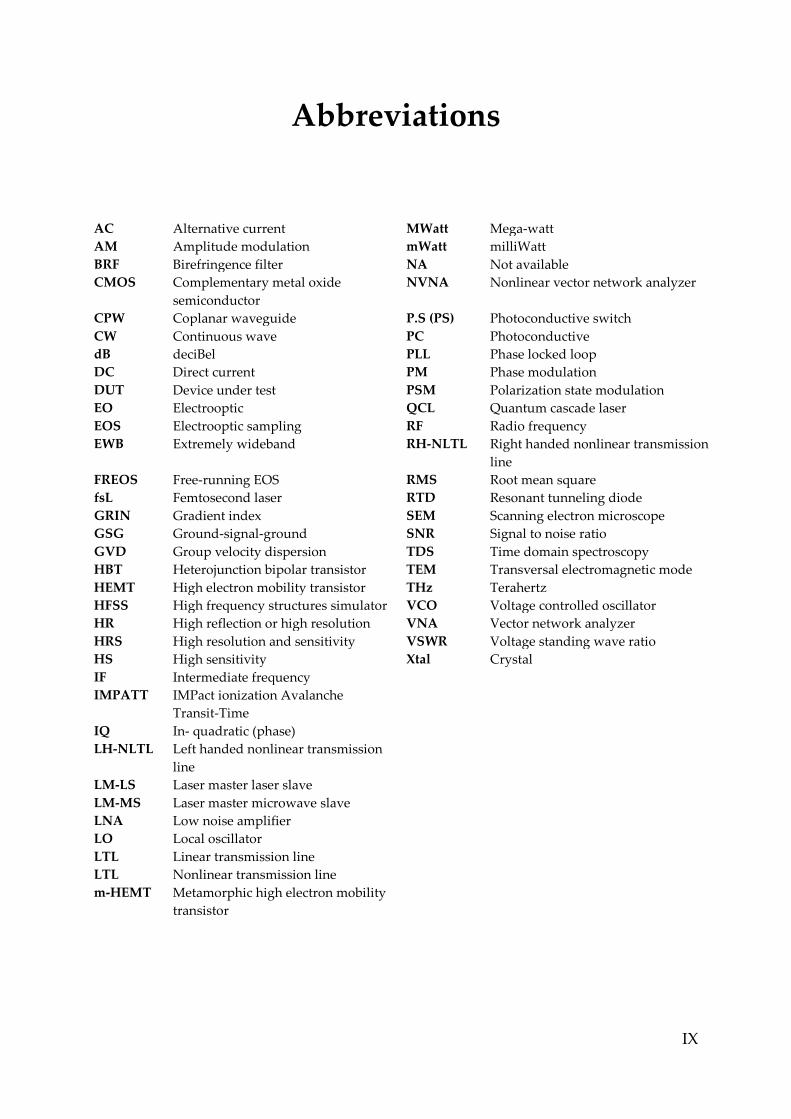
Abbreviations
AC Alternative current MWatt Mega-watt
AM Amplitude modulation mWatt milliWatt
BRF Birefringence filter NA Not available
CMOS Complementary metal oxide
semiconductor
NVNA Nonlinear vector network analyzer
CPW Coplanar waveguide P.S (PS) Photoconductive switch
CW Continuous wave PC Photoconductive
dB deciBel PLL Phase locked loop
DC Direct current PM Phase modulation
DUT Device under test PSM Polarization state modulation
EO Electrooptic QCL Quantum cascade laser
EOS Electrooptic sampling RF Radio frequency
EWB Extremely wideband RH-NLTL Right handed nonlinear transmission
line
FREOS Free-running EOS RMS Root mean square
fsL Femtosecond laser RTD Resonant tunneling diode
GRIN Gradient index SEM Scanning electron microscope
GSG Ground-signal-ground SNR Signal to noise ratio
GVD Group velocity dispersion TDS Time domain spectroscopy
HBT Heterojunction bipolar transistor TEM Transversal electromagnetic mode
HEMT High electron mobility transistor THz Terahertz
HFSS High frequency structures simulator VCO Voltage controlled oscillator
HR High reflection or high resolution VNA Vector network analyzer
HRS High resolution and sensitivity VSWR Voltage standing wave ratio
HS High sensitivity Xtal Crystal
IF Intermediate frequency
IMPATT IMPact ionization Avalanche
Transit-Time
IQ In- quadratic (phase)
LH-NLTL Left handed nonlinear transmission
line
LM-LS Laser master laser slave
LM-MS Laser master microwave slave
LNA Low noise amplifier
LO Local oscillator
LTL Linear transmission line
LTL Nonlinear transmission line
m-HEMT Metamorphic high electron mobility
transistor

XI
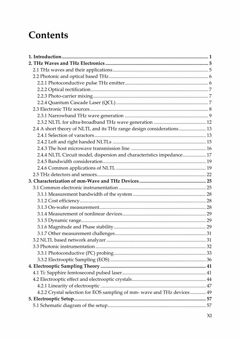
Contents
Introduction ......................................................................................................................... 1 1.
THz Waves and THz Electronics ..................................................................................... 5 2.
2.1 THz waves and their applications ............................................................................... 5
2.2 Photonic and optical based THz .................................................................................. 6
Photoconductive pulse THz emitter ..................................................................... 6 2.2.1
Optical rectification ................................................................................................. 7 2.2.2
Photo-carrier mixing ............................................................................................... 7 2.2.3
Quantum Cascade Laser (QCL) ............................................................................ 7 2.2.4
2.3 Electronic THz sources .................................................................................................. 8
Narrowband THz wave generation ..................................................................... 9 2.3.1
NLTL for ultra-broadband THz wave generation ........................................... 12 2.3.2
2.4 A short theory of NLTL and its THz range design considerations ...................... 13
Selection of varactors ............................................................................................ 13 2.4.1
Left and right handed NLTLs ............................................................................. 15 2.4.2
The host microwave transmission line .............................................................. 16 2.4.3
NLTL Circuit model, dispersion and characteristics impedance ................... 17 2.4.4
Bandwidth consideration ..................................................................................... 19 2.4.5
Common applications of NLTL .......................................................................... 19 2.4.6
2.5 THz detectors and sensors .......................................................................................... 22
Characterization of mm-Wave and THz Devices ....................................................... 25 3.
3.1 Common electronic instrumentation ........................................................................ 25
Measurement bandwidth of the system ............................................................ 28 3.1.1
Cost efficiency ........................................................................................................ 28 3.1.2
On-wafer measurement ........................................................................................ 28 3.1.3
Measurement of nonlinear devices ..................................................................... 29 3.1.4
Dynamic range....................................................................................................... 29 3.1.5
Magnitude and Phase stability ............................................................................ 29 3.1.6
Other measurement challenges ........................................................................... 31 3.1.7
3.2 NLTL based network analyzer .................................................................................. 31
3.3 Photonic instrumentation ........................................................................................... 32
Photoconductive (PC) probing ............................................................................ 33 3.3.1
Electrooptic Sampling (EOS) ............................................................................... 36 3.3.2
Electrooptic Sampling Theory ....................................................................................... 41 4.
4.1 Ti: Sapphire femtosecond pulsed laser ..................................................................... 41
4.2 Electrooptic effect and electrooptic crystals ............................................................. 44
Linearity of electrooptic ....................................................................................... 47 4.2.1
Crystal selection for EOS sampling of mm- wave and THz devices ............. 49 4.2.2
Electrooptic Setup............................................................................................................. 57 5.
5.1 Schematic diagram of the setup ................................................................................. 57
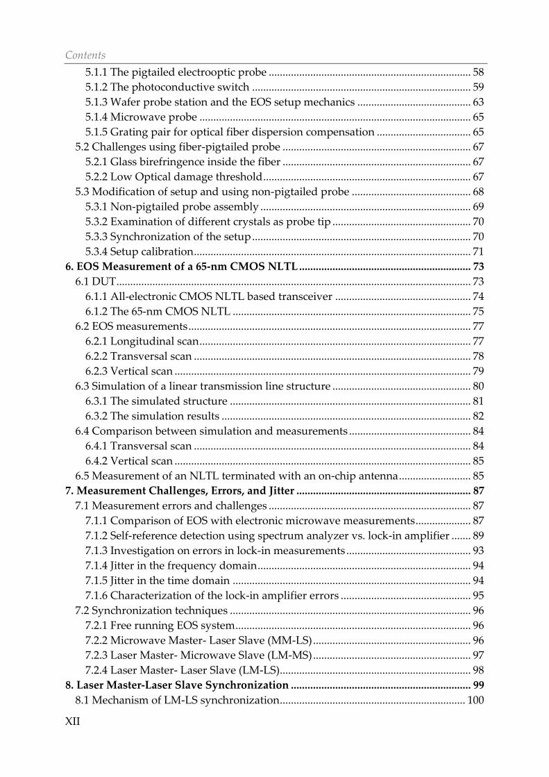
Contents
XII
The pigtailed electrooptic probe ......................................................................... 58 5.1.1
The photoconductive switch ............................................................................... 59 5.1.2
Wafer probe station and the EOS setup mechanics ......................................... 63 5.1.3
Microwave probe .................................................................................................. 65 5.1.4
Grating pair for optical fiber dispersion compensation .................................. 65 5.1.5
5.2 Challenges using fiber-pigtailed probe .................................................................... 67
Glass birefringence inside the fiber .................................................................... 67 5.2.1
Low Optical damage threshold ........................................................................... 67 5.2.2
5.3 Modification of setup and using non-pigtailed probe ........................................... 68
Non-pigtailed probe assembly ............................................................................ 69 5.3.1
Examination of different crystals as probe tip .................................................. 70 5.3.2
Synchronization of the setup ............................................................................... 70 5.3.3
Setup calibration .................................................................................................... 71 5.3.4
EOS Measurement of a 65-nm CMOS NLTL .............................................................. 73 6.
6.1 DUT ................................................................................................................................ 73
All-electronic CMOS NLTL based transceiver ................................................. 74 6.1.1
The 65-nm CMOS NLTL ...................................................................................... 75 6.1.2
6.2 EOS measurements ...................................................................................................... 77
Longitudinal scan .................................................................................................. 77 6.2.1
Transversal scan .................................................................................................... 78 6.2.2
Vertical scan ........................................................................................................... 79 6.2.3
6.3 Simulation of a linear transmission line structure .................................................. 80
The simulated structure ....................................................................................... 81 6.3.1
The simulation results .......................................................................................... 82 6.3.2
6.4 Comparison between simulation and measurements ............................................ 84
Transversal scan .................................................................................................... 84 6.4.1
Vertical scan ........................................................................................................... 85 6.4.2
6.5 Measurement of an NLTL terminated with an on-chip antenna .......................... 85
Measurement Challenges, Errors, and Jitter ............................................................... 87 7.
7.1 Measurement errors and challenges ......................................................................... 87
Comparison of EOS with electronic microwave measurements .................... 87 7.1.1
Self-reference detection using spectrum analyzer vs. lock-in amplifier ....... 89 7.1.2
Investigation on errors in lock-in measurements ............................................. 93 7.1.3
Jitter in the frequency domain ............................................................................. 94 7.1.4
Jitter in the time domain ...................................................................................... 94 7.1.5
Characterization of the lock-in amplifier errors ............................................... 95 7.1.6
7.2 Synchronization techniques ....................................................................................... 96
Free running EOS system ..................................................................................... 96 7.2.1
Microwave Master- Laser Slave (MM-LS) ......................................................... 96 7.2.2
Laser Master- Microwave Slave (LM-MS) ......................................................... 97 7.2.3
Laser Master- Laser Slave (LM-LS) ..................................................................... 98 7.2.4
Laser Master-Laser Slave Synchronization ................................................................. 99 8.
8.1 Mechanism of LM-LS synchronization ................................................................... 100
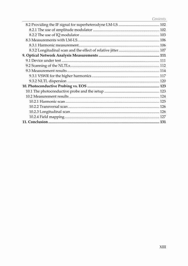
Contents
XIII
8.2 Providing the IF signal for superheterodyne LM-LS ........................................... 102
The use of amplitude modulator ...................................................................... 102 8.2.1
The use of IQ modulator .................................................................................... 103 8.2.2
8.3 Measurements with LM-LS ...................................................................................... 106
Harmonic measurement ..................................................................................... 106 8.3.1
Longitudinal scan and the effect of relative jitter ........................................... 107 8.3.2
Optical Network Analysis Measurements ................................................................ 111 9.
9.1 Device under test ....................................................................................................... 111
9.2 Scanning of the NLTLs .............................................................................................. 112
9.3 Measurement results ................................................................................................. 114
VSWR for the higher harmonics ....................................................................... 117 9.3.1
NLTL dispersion ................................................................................................. 120 9.3.2
Photoconductive Probing vs. EOS ............................................................................ 123 10.
10.1 The photoconductive probe and the setup .......................................................... 123
10.2 Measurement results ............................................................................................... 124
Harmonic scan ................................................................................................... 125 10.2.1
Transversal scan ................................................................................................ 126 10.2.2
Longitudinal scan .............................................................................................. 126 10.2.3
Field mapping .................................................................................................... 127 10.2.4
Conclusion ..................................................................................................................... 131 11.

1
Introduction 1.
THz waves with the electromagnetic spectrum lying between microwave and optics
are nowadays widely used in many applications such as material inspection,
explosive detection, medicine and astronomy. This interest has motivated scientists
to explore new methods for generation and detection of THz waves. THz waves can
be generated with different techniques, and more conventional ways are based on
optics and photonic. The use of femtosecond laser in conjunction with
photoconductive antennas to emitting THz waves and quantum cascade lasers are
examples. These methods suffer from drawbacks such as the need for costly and
bulky instruments like lasers or cryogenic cooling systems which make them
inappropriate for portable applications. Alternatively, electronic approaches for
realizing THz systems have great advantages as illustrate compact and cheap
solutions for future availability of THz waves. Despite these outstanding advantages,
it is extremely challenging to push electronic devices to operate at very high
frequencies of THz. Fortunately recent development in electronic technology and
scaling has opened new doors in this field. Recently THz electronic devices have
been made using ultrafast Schottky diodes with the cut-off frequency in a range of
tens of THz or ultrafast transistors such as InP-HEMT whose fmax lies in THz range.
On the other side, targeting THz waves with electronics has also made significant
progress in the development of mm-waves devices and expanded the high frequency
market.
By increasing the speed of electronic devices towards THz range, their
characterization poses new challenges as we need instruments faster than the devices
under test (DUTs). In a worst case scenario, if one makes a device faster than the
conventional instruments, he/she should look for another characterization
alternative. The good news is that newly fabricated high speed devices can also be
utilized in instrumentation, as recently have been demonstrated by Schottky diode
based extended modules [1] in network analyzers. This has extended their
Chapter 1. Introduction
2
measurement bandwidth beyond 1 THz which covers more than the required
bandwidth of the most today’s ultrafast electronics. Although this is very favorable,
these kinds of instruments are in their infancy and need improvement. Notably, since
at THz frequencies it is extremely difficult to precisely model device contact probes
and calibration kits, systematic errors in measurements can be increased. Another
drawback of using these instruments is the high cost of setup components and time
consuming measurements. This can be imagined for a full-band measurement of an
ultra-broadband device, as with this approach one needs to perform band-to-band
measurements by changing waveguide sets and performing several times of
calibrations.
In contrast to the electronic systems, the photonics and optical approaches
such as photoconductive (PC) probing and Electrooptic Sampling (EOS) offer an
ultra-broadband measurement bandwidth from DC to several THz. These systems
also require much less calibration of the setups during measurements which lead to
having fewer errors. Also in comparison to electronic approach, they present
interesting features such as near field sensing and imaging with the use of a
contactless positionable probe. In particular, EOS using an electrooptic (EO) crystal
probe with very high spatial resolution and almost a flat frequency response in the
detection is a superior solution for ultrafast electronic devices characterization. These
unique properties of EOS are the motivation to use it in this thesis.
The history of EOS refers to 1983 where Valdmanis et al. [2] for the first time
introduced it using the picosecond lasers. It was more development after the
invention and the use of the femtosecond pulse lasers in the 90 s which highly
extended the measurement bandwidth of EOS for the purpose of ultrafast electronic
characterization. It can be assumed that a typical 100 fs of laser pulse-width
theoretically guarantees measurement bandwidth up to 10 THz which is much
beyond the operating frequency of today’s electronics. In other words, since the 90 s,
EOS as an ultrafast optical approach is capable to measure THz devices. However,
there were not such devices available at that period of time. The recent progress in
increasing the operating frequency of electronic devices towards THz can be a strong
convincing reason to use this high speed technique for their characterization.
The main objective of this work is to characterize an all-electronic THz device
which is designed based on Nonlinear Transmission Line (NLTL), in the framework
of ULTRA project [3]. This device acting as a harmonic generator can be used for
frequency up/down-conversion in a superheterodyne transceiver for the applications
such as mm-wave or THz spectroscopy. The device was designed by Philips [4] as
our project partner and fabricated using the 65-nm CMOS technology at TSMC® [5].
Chapter 1. Introduction
3
Since in this work both DUT and characterization methods are important,
before demonstrating results, the state-of-the-art in THz electronics and their
common ways of characterization are reviewed. In follow-up, the principle and
theory of NLTL as an ultra-broadband THz DUT is also introduced and theoretically
described. Since this device is theoretically designed to operate from microwave to
THz, therefore, an ultra-broadband characterization system like EOS is required. On
the other hand, the device itself can also be used to figure out the limitations of the
EOS in terms of measurement bandwidth.
Most of the previous works have shown a very broadband EOS for the
characterization of passive components in the pump-probe regime and only a few
attempts have been made for active nonlinear components. This work, by
differentiating between EOS for passive and actives components, highlights why
reaching an ultrahigh-bandwidth in the latter is much challenging than another. In
contrast to pump-probe EOS for passive components such as transmission lines, in
CW excitation of nonlinear devices, we may lose most of the potential of system
bandwidth due to facing with jitter and more specifically, at higher frequencies the
signal to noise degrades drastically. Resolving these challenges, which for years has
remained as the major prohibiting factor in EOS, is targeted in this work.
Accordingly, the most critical part of jitter which is relative jitter between the source
and the sampling laser pulse is studied and finally with a novel approach fully
resolved. It can be said that this solution, called laser master laser slave (LM-LS)
configuration, for the first time is introduced here for the integration with EOS. This
scheme makes the system fully coherent and allows recovering an ultra-broad
measurement bandwidth.

5
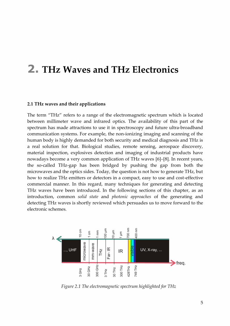
THz Waves and THz Electronics 2.
2.1 THz waves and their applications
The term “THz” refers to a range of the electromagnetic spectrum which is located
between millimeter wave and infrared optics. The availability of this part of the
spectrum has made attractions to use it in spectroscopy and future ultra-broadband
communication systems. For example, the non-ionizing imaging and scanning of the
human body is highly demanded for both security and medical diagnosis and THz is
a real solution for that. Biological studies, remote sensing, aerospace discovery,
material inspection, explosives detection and imaging of industrial products have
nowadays become a very common application of THz waves [6]–[8]. In recent years,
the so-called THz-gap has been bridged by pushing the gap from both the
microwaves and the optics sides. Today, the question is not how to generate THz, but
how to realize THz emitters or detectors in a compact, easy to use and cost-effective
commercial manner. In this regard, many techniques for generating and detecting
THz waves have been introduced. In the following sections of this chapter, as an
introduction, common solid state and photonic approaches of the generating and
detecting THz waves is shortly reviewed which persuades us to move forward to the
electronic schemes.
1 µ
m
70
0 n
m
100
µm
1 m
m
1 c
m
10 c
m
10
µm
40
0 n
m
mic
row
ave
mm
- wave
TH
z
Fa
r- IR
vis
ible
freq.
λ
UV, X-ray, ...IR
300
TH
z
428
TH
z
3 T
Hz
300
GH
z
30 G
Hz
3 G
Hz
30
TH
z
74
9 T
Hz
..., UHF
Figure 2.1 The electromagnetic spectrum highlighted for THz
Chapter 2. THz Waves and THz Electronics
6
2.2 Photonic and optical based THz
The term “THz gap” is a reminder that THz was hard to achieve or may only be
generated at low power, but this has proven not to be the case nowadays as the
amount of radiated power can vary in a very broad range from microwatts to
MWatts. In this regard, while low power systems are appropriate for lab-scale
applications such as material inspection and imaging, remote sensing and future
communication systems based on THz require very high power solutions to
compensate the path losses. In general, based on the amount of emitted power and
the application, THz generators can be classified into three categories as follows
Very high power THz, with nearly 1 MW which can be generated by
Gyrotrons [9]–[11], klystrons or traveling wave tubes (TWTs)[7], [8], [12] and
usually they work at lower THz bands towards mm-waves.
High power THz with emitting several Watts which can be generated with
the aid of free electron lasers [10],[13].
Medium and low power THz (less than tens of milli-Watts) which can be
generated using laser and solid states.
In the following sections more common methods of generating THz are
explained.
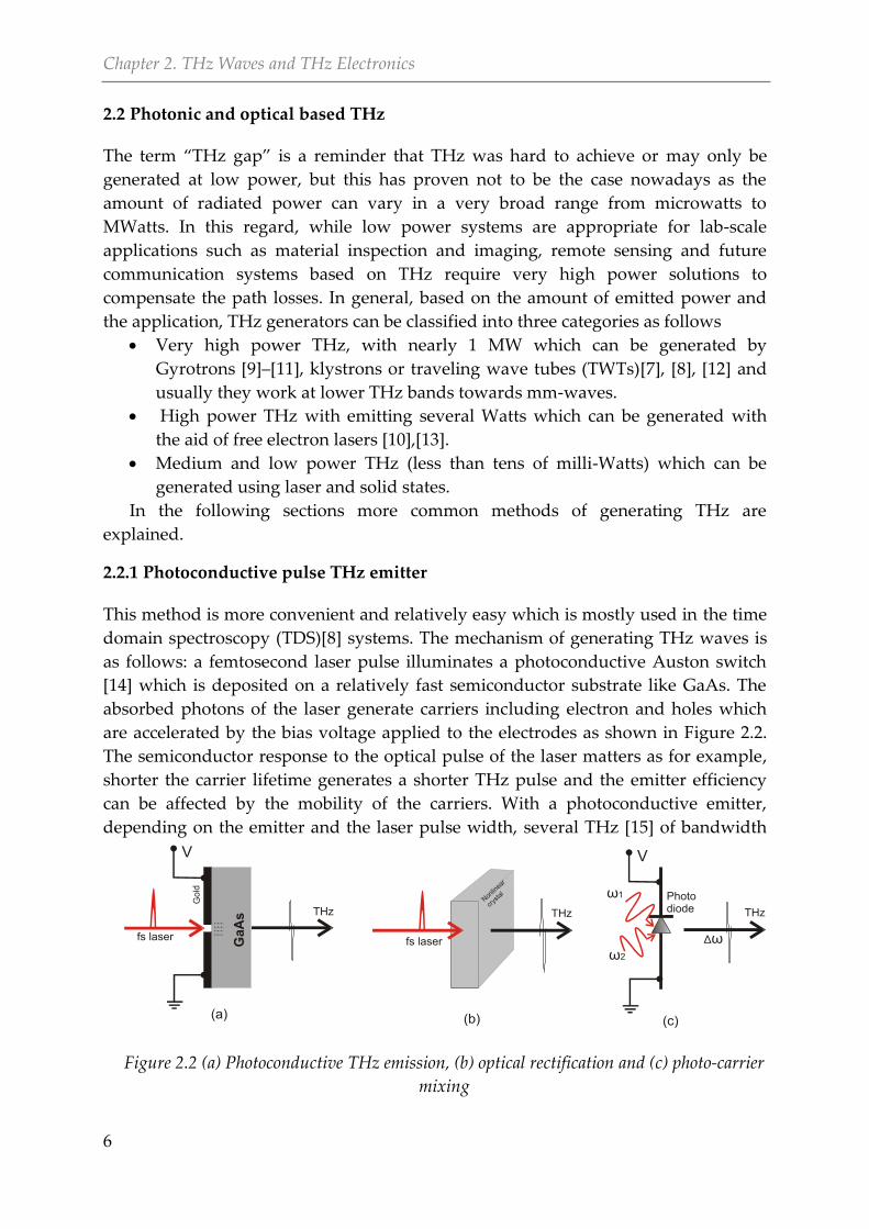
Photoconductive pulse THz emitter 2.2.1
This method is more convenient and relatively easy which is mostly used in the time
domain spectroscopy (TDS)[8] systems. The mechanism of generating THz waves is
as follows: a femtosecond laser pulse illuminates a photoconductive Auston switch
[14] which is deposited on a relatively fast semiconductor substrate like GaAs. The
absorbed photons of the laser generate carriers including electron and holes which
are accelerated by the bias voltage applied to the electrodes as shown in Figure 2.2.
The semiconductor response to the optical pulse of the laser matters as for example,
shorter the carrier lifetime generates a shorter THz pulse and the emitter efficiency
can be affected by the mobility of the carriers. With a photoconductive emitter,
depending on the emitter and the laser pulse width, several THz [15] of bandwidth
Non
linea
r
crys
tal
GaA
s
fs laser fs laser
THzTHz+-+-+-+-+-+-+-+-+-+-+-+-
Gold
V
THz
V
ω1
ω2
Δω
(a) (b) (c)
Photo diode
Figure 2.2 (a) Photoconductive THz emission, (b) optical rectification and (c) photo-carrier
mixing
2.2. Photonic and optical based THz
7
can be achieved. A major drawback of this scheme is a very low conversion efficiency
of the optical energy to THz and typically pumping a photoconductive emitter with 1
Watt of the optical power will generate only sub-milli-Watt of the THz power.
Optical rectification 2.2.2
In this technique, a nonlinear optical crystal like LiNbO3 can be used to generate THz
waves based on the second order nonlinear polarization effect [16], determined by
( ) where
( ) (2.1)
is the material susceptibility. The THz waves can be generated by optical mixing of
two different wavelengths of CW lasers or the intrinsic spectrum of a single
femtosecond (fs) pulse [17], [18]. In the latter, each wave component in the spectrum
band of , due to the nonlinearity of the medium, mixes with the rest resulting in
new photon generation in the THz range. More clearly, two wavelengths λ1 and λ2
with the offset frequency of Δω= ω1-ω2, which lies in the THz range are mix with each
other to generate a THz signal. The method of optical rectification is known as the
most broadband THz wave generation scheme ever. However, the amount of the
emitted power is limited by the very small electrooptic coefficient of the crystal.
Figure 2.2 (b) shows a very simple schematic of this scheme.
Photo-carrier mixing 2.2.3
Comparable to the optical rectification, this scheme in principle also needs two
wavelengths to generate a beat frequency at THz range. Despite this similarity, it
uses a different mechanism of photonic mixing usually using two CW lasers as
shown in Figure 2.2 (c). Assuming two laser beams at optical frequencies of
, the mixed signal can be derived as:
| | ( ) | | ( )
=
| || |[ [( ) ] [ [( ) ]
(2.2)
while the beat frequency of lies in the THz frequency range and the
sum of the frequencies remains in the optical range much beyond the optical
frequency used. The latter term is rejected by the low pass filtering of the photo
mixer.
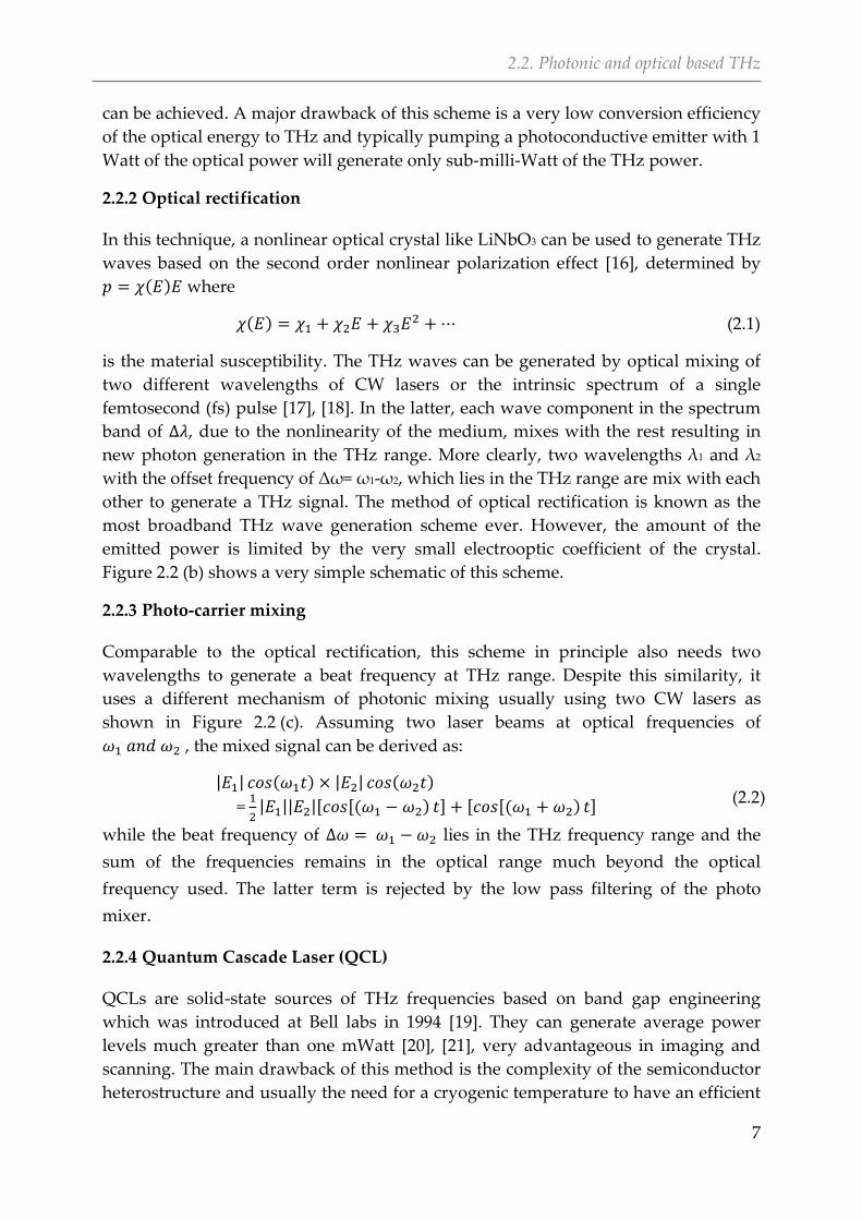
Quantum Cascade Laser (QCL) 2.2.4
QCLs are solid-state sources of THz frequencies based on band gap engineering
which was introduced at Bell labs in 1994 [19]. They can generate average power
levels much greater than one mWatt [20], [21], very advantageous in imaging and
scanning. The main drawback of this method is the complexity of the semiconductor
heterostructure and usually the need for a cryogenic temperature to have an efficient
Chapter 2. THz Waves and THz Electronics
8
performance. To build up a QCL, the bandgap structure of semiconductor material
must be reengineered. For example, for GaAs, which has a bandgap at infrared (800
nm), inter-sub-band gaps or in other words, quantum wells are required. This can be
realized by placing thin periodic layers of materials such as AlGaAs in a form of
super-lattice composition. The thickness of the layers tunes the emitted wavelength.
Figure 2.3 shows the mechanism of THz wave radiation in a QCL [22] [23].
2.3 Electronic THz sources
A drawback of most of the techniques presented before is that they operate in lab-
scale and may need expensive and bulky lasers or cryogenic cooling systems. On the
contrary, the electronic approach is an alternative which can make the availability of
THz waves in a cheap, compact and massive industrial solution. In this approach,
people from the microwave side are attempting to increase the performance of the
electronic devices to make them operational at THz range as recently several devices
and systems have been demonstrated. Despite a huge interest, unfortunately, this
approach suffers from certain technology limitations. Although the aggressive
scaling can help to increase the speed of the devices, it is still limited by the carrier
drift-velocity saturation and reduces the tolerance of devices in power handling. For
example, even a very low power applied at the gate of a field effect device, which has
only tens of nanometer length can harm it. However, these limitations should not be
disappointing as researchers have found several ways to improve them.
Since the scope of this work is to characterize THz electronic devices, recent
advances in THz electronics are significantly important for us. Therefore, in the next
sections of this chapter, the literature is reviewed in this regard.
Figure 2.3 Schematic of multilayer structure for generation of quantum wells in a quantum
cascade laser (a) and (b) mechanism of THz wave radiation from sub-bands.
2.3. Electronic THz sources
9
Narrowband THz wave generation 2.3.1
Direct oscillation at THz frequencies
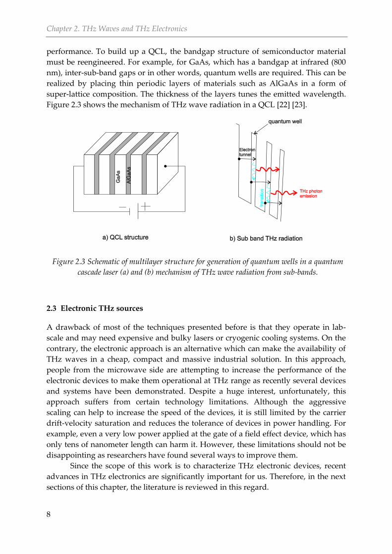
One way of generating THz waves is to make a direct oscillation at THz frequencies
by applying a DC bias to a Resonant Tunneling Diode (RTD) [24]. Looking at I-V
curves of a typical RTD depicted in Figure 2.4, the negative differential resistance is
identified as the origin of this oscillation. Unfortunately, the efficiency of this scheme
is very low and only a very small portion of the power at THz range can be radiated.
In [25] the main reason for this low power efficiency is attributed to the narrow
voltage range in the negative resistance area (see Figure 2.4) which makes the output
power defined by P= ΔI×ΔV small. Moreover, the semiconductor used must be
engineered carefully to be operational at the THz frequencies.
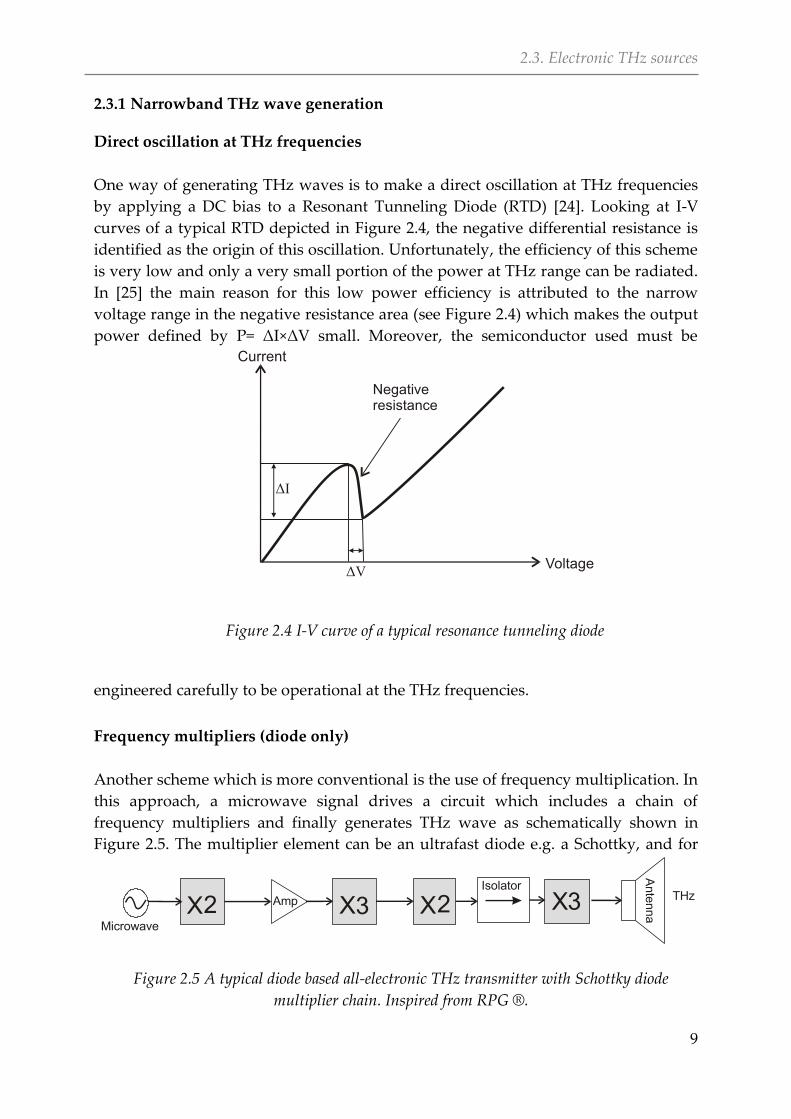
Frequency multipliers (diode only)
Another scheme which is more conventional is the use of frequency multiplication. In
this approach, a microwave signal drives a circuit which includes a chain of
frequency multipliers and finally generates THz wave as schematically shown in
Figure 2.5. The multiplier element can be an ultrafast diode e.g. a Schottky, and for
Negative resistance
ΔI
ΔVVoltage
Current
Figure 2.4 I-V curve of a typical resonance tunneling diode
Microwave
2X X X X3 2 3Isolator
Ante
nna
Amp THz
Figure 2.5 A typical diode based all-electronic THz transmitter with Schottky diode
multiplier chain. Inspired from RPG ®.
Chapter 2. THz Waves and THz Electronics
10
achieving higher power at the output, the signal may be amplified in the primary
stages using ultrafast transistors such as III/V heterojunction bipolar transistor (HBT),
HEMT or metamorphic HEMT (mHEMT).
Diodes can operate at very high frequencies and have already commercially
been adapted to THz systems [26], [27]. IMPATT (IMPact ionization Avalanche
Transit-Time) diode, Gunn diode, RTD (resonant tunneling diodes) and SBD
(Schottky barrier diodes) are widely used in these kinds of technologies. The major
drawback of using diodes in a frequency multiplier is their passive upconversion
(mixing) mechanism, as they exhibit no gain. This shortage results in a very large
conversion loss as with pumping power of hundreds of milli-Watts a THz signal with
only a few microwatts can be achieved [8], [28]. If such a multiplier is being used for
down conversion of a receiving signal, due to the lack of having a low noise amplifier
(LNA) at THz frequencies in the first stage, the signal to noise ratio (SNR)
dramatically degrades. Moreover, designing Schottky diode based multipliers at
frequencies above 2 THz is a challenge due to the size of the chip and the waveguide
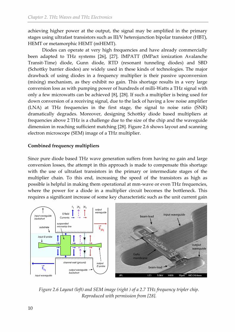
dimension in reaching sufficient matching [28]. Figure 2.6 shows layout and scanning
electron microscope (SEM) image of a THz multiplier.
Combined frequency multipliers
Since pure diode based THz wave generation suffers from having no gain and large
conversion losses, the attempt in this approach is made to compensate this shortage
with the use of ultrafast transistors in the primary or intermediate stages of the
multiplier chain. To this end, increasing the speed of the transistors as high as
possible is helpful in making them operational at mm-wave or even THz frequencies,
where the power for a diode in a multiplier circuit becomes the bottleneck. This
requires a significant increase of some key characteristic such as the unit current gain
Figure 2.6 Layout (left) and SEM image (right ) of a 2.7 THz frequency tripler chip.
Reproduced with permission from [28].
2.3. Electronic THz sources
11
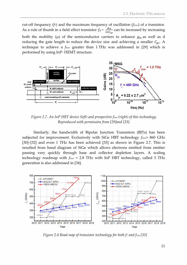
cut-off frequency (fT) and the maximum frequency of oscillation (fmax) of a transistor.
As a rule of thumb in a field effect transistor
can be increased by increasing
both the mobility (μ) of the semiconductor carriers to enhance as well as d
reducing the gate length to reduce the device size and achieving a smaller . A
technique to achieve a fmax greater than 1 THz was addressed in [29] which is
performed by using InP- HEMT structure.
Similarly, the bandwidth of Bipolar Junction Transistors (BJTs) has been
subjected for improvement. Exclusively with SiGe HBT technology fmax> 860 GHz
[30]–[32] and even 1 THz has been achieved [33] as shown in Figure 2.7. This is
resulted from band diagram of SiGe which allows electrons emitted from emitter
passing very quickly through base and collector depletion layers. A scaling
technology roadmap with fmax = 2.8 THz with InP HBT technology, called 3 THz
generation is also addressed in [34].
Figure 2.8 Road map of transistor technology for both fT and fmax [35]
Figure 2.7. An InP HBT device (left) and prospective fmax (right) of this technology.
Reproduced with permission from [29]and [33].
Chapter 2. THz Waves and THz Electronics
12
All of the utilized technologies in the field of THz electronics are pushing to
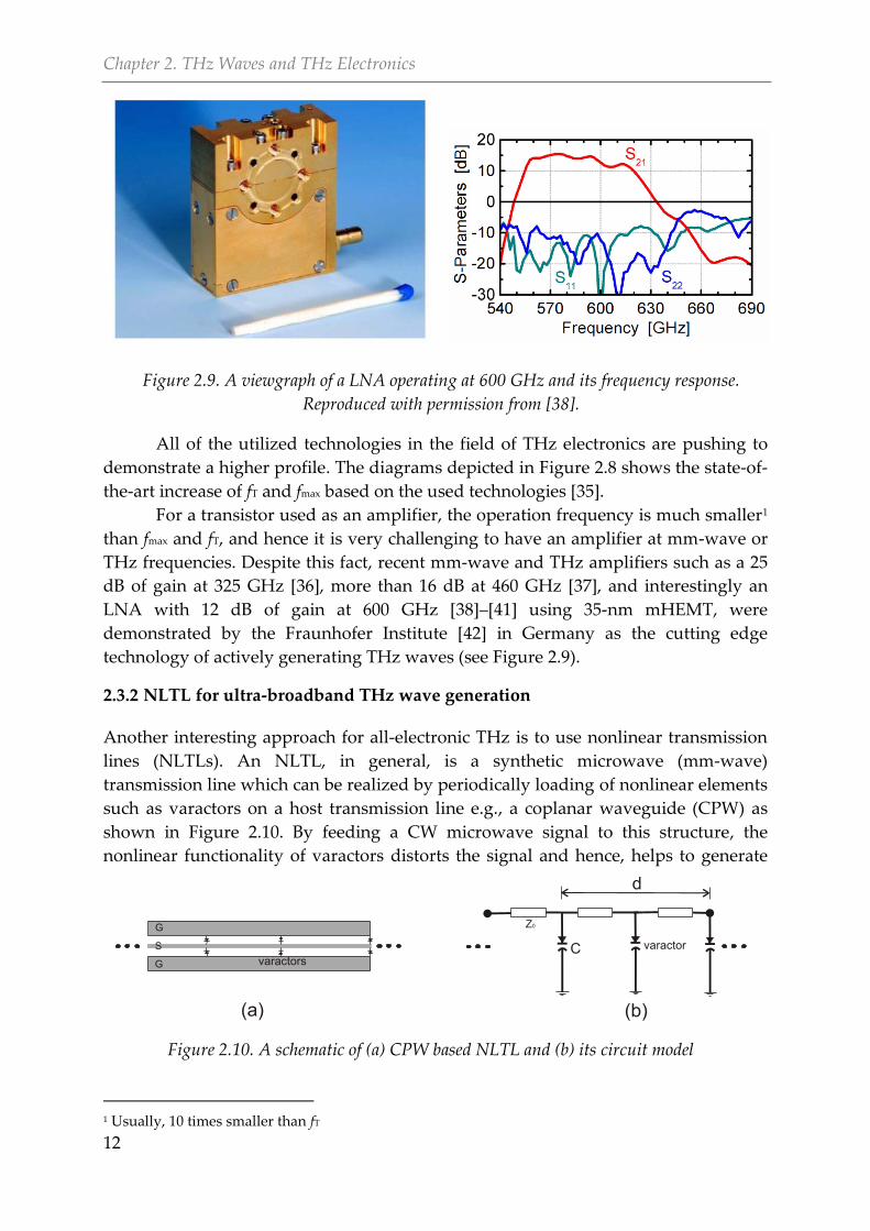
demonstrate a higher profile. The diagrams depicted in Figure 2.8 shows the state-of-
the-art increase of fT and fmax based on the used technologies [35].
For a transistor used as an amplifier, the operation frequency is much smaller1
than fmax and fT, and hence it is very challenging to have an amplifier at mm-wave or
THz frequencies. Despite this fact, recent mm-wave and THz amplifiers such as a 25
dB of gain at 325 GHz [36], more than 16 dB at 460 GHz [37], and interestingly an
LNA with 12 dB of gain at 600 GHz [38]–[41] using 35-nm mHEMT, were
demonstrated by the Fraunhofer Institute [42] in Germany as the cutting edge
technology of actively generating THz waves (see Figure 2.9). [43]
NLTL for ultra-broadband THz wave generation 2.3.2
Another interesting approach for all-electronic THz is to use nonlinear transmission
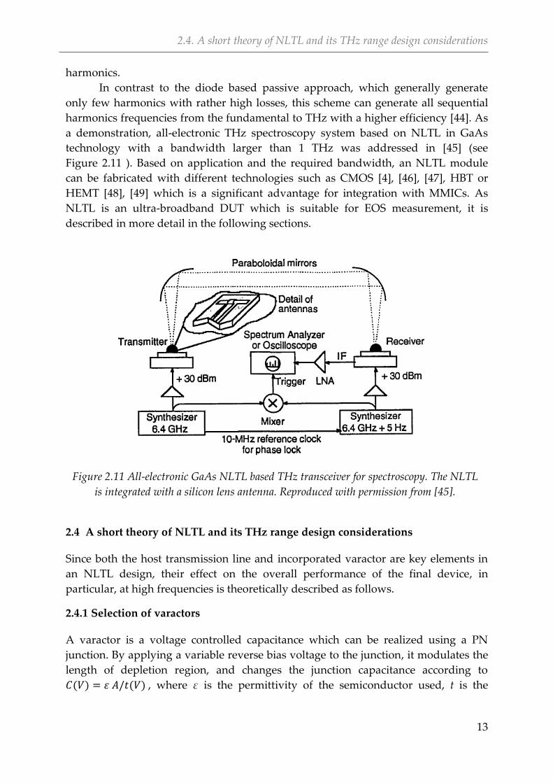
lines (NLTLs). An NLTL, in general, is a synthetic microwave (mm-wave)
transmission line which can be realized by periodically loading of nonlinear elements
such as varactors on a host transmission line e.g., a coplanar waveguide (CPW) as
shown in Figure 2.10. By feeding a CW microwave signal to this structure, the
nonlinear functionality of varactors distorts the signal and hence, helps to generate
1 Usually, 10 times smaller than fT
Figure 2.9. A viewgraph of a LNA operating at 600 GHz and its frequency response.
Reproduced with permission from [38].
C
Z0
varactor
(a) (b)
G
G
S
varactors
Figure 2.10. A schematic of (a) CPW based NLTL and (b) its circuit model
2.4. A short theory of NLTL and its THz range design considerations
13
harmonics.
In contrast to the diode based passive approach, which generally generate
only few harmonics with rather high losses, this scheme can generate all sequential
harmonics frequencies from the fundamental to THz with a higher efficiency [44]. As
a demonstration, all-electronic THz spectroscopy system based on NLTL in GaAs
technology with a bandwidth larger than 1 THz was addressed in [45] (see
Figure 2.11 ). Based on application and the required bandwidth, an NLTL module
can be fabricated with different technologies such as CMOS [4], [46], [47], HBT or
HEMT [48], [49] which is a significant advantage for integration with MMICs. As
NLTL is an ultra-broadband DUT which is suitable for EOS measurement, it is
described in more detail in the following sections.
2.4 A short theory of NLTL and its THz range design considerations
Since both the host transmission line and incorporated varactor are key elements in
an NLTL design, their effect on the overall performance of the final device, in
particular, at high frequencies is theoretically described as follows.
Selection of varactors 2.4.1
A varactor is a voltage controlled capacitance which can be realized using a PN
junction. By applying a variable reverse bias voltage to the junction, it modulates the
length of depletion region, and changes the junction capacitance according to
( ) ( ) , where ε is the permittivity of the semiconductor used, t is the
Figure 2.11 All-electronic GaAs NLTL based THz transceiver for spectroscopy. The NLTL
is integrated with a silicon lens antenna. Reproduced with permission from [45].
Chapter 2. THz Waves and THz Electronics
14
voltage dependent variable length of depletion region and A is cross section area of
the junction respectively.
It is notable that any diode with reverse bias can be used but for ultra-high
speed and THz applications, Schottky and resonant tunneling diodes (RTD) in III-IV
technology are preferred. The latter can also amplify the signal by its negative
differential resistance. Another alternative, which is more convenient for designers
and rather cheaper in the technology, is CMOS varactor. A broad range of
application from a multi-gigahertz voltage controlled oscillators (VCOs) to millimeter
wave NLTLs [4], [46] have been addressed using these kinds of varactors. Also, the
scaling of CMOS technology has made new varactors which are more attractive for
ultrafast designers [50].
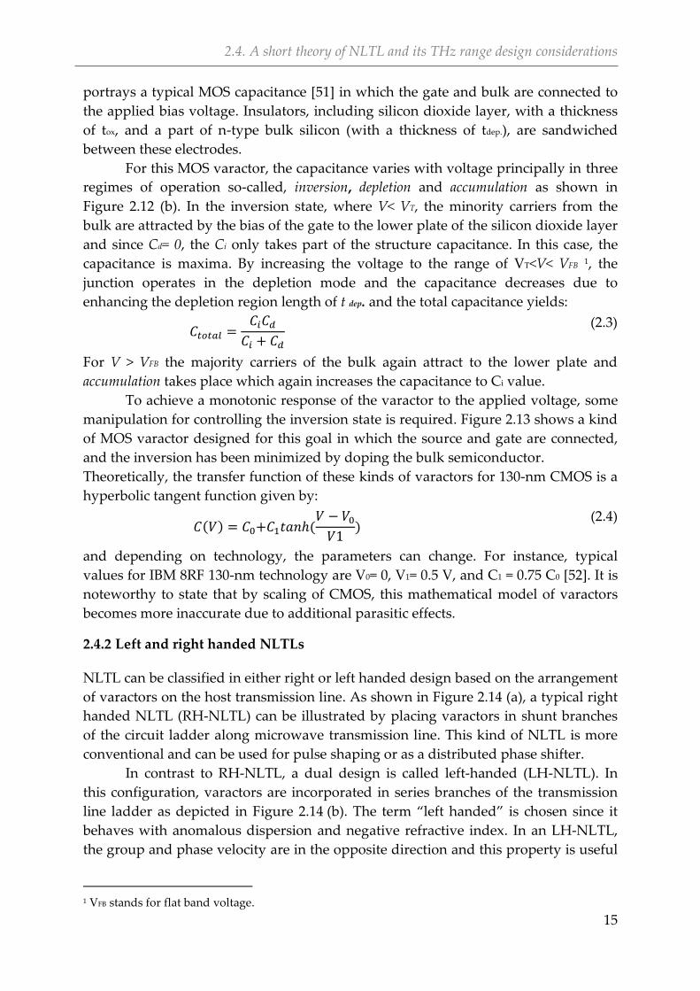
Since CMOS varactor is frequently mentioned in this work, at this point it is
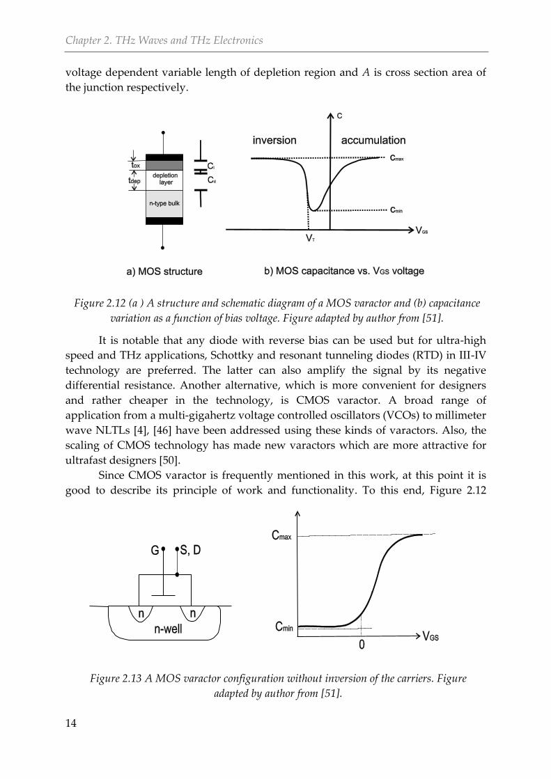
good to describe its principle of work and functionality. To this end, Figure 2.12
Figure 2.13 A MOS varactor configuration without inversion of the carriers. Figure
adapted by author from [51].
Figure 2.12 (a ) A structure and schematic diagram of a MOS varactor and (b) capacitance
variation as a function of bias voltage. Figure adapted by author from [51].
2.4. A short theory of NLTL and its THz range design considerations
15
portrays a typical MOS capacitance [51] in which the gate and bulk are connected to
the applied bias voltage. Insulators, including silicon dioxide layer, with a thickness
of tox, and a part of n-type bulk silicon (with a thickness of tdep.), are sandwiched
between these electrodes.
For this MOS varactor, the capacitance varies with voltage principally in three
regimes of operation so-called, inversion, depletion and accumulation as shown in
Figure 2.12 (b). In the inversion state, where V< VT, the minority carriers from the
bulk are attracted by the bias of the gate to the lower plate of the silicon dioxide layer
and since Cd= 0, the Ci only takes part of the structure capacitance. In this case, the
capacitance is maxima. By increasing the voltage to the range of VT<V< VFB 1, the
junction operates in the depletion mode and the capacitance decreases due to
enhancing the depletion region length of t dep. and the total capacitance yields:
(2.3)
For V > VFB the majority carriers of the bulk again attract to the lower plate and
accumulation takes place which again increases the capacitance to Ci value.
To achieve a monotonic response of the varactor to the applied voltage, some
manipulation for controlling the inversion state is required. Figure 2.13 shows a kind
of MOS varactor designed for this goal in which the source and gate are connected,
and the inversion has been minimized by doping the bulk semiconductor.
Theoretically, the transfer function of these kinds of varactors for 130-nm CMOS is a
hyperbolic tangent function given by:
( ) (
)
(2.4)
and depending on technology, the parameters can change. For instance, typical
values for IBM 8RF 130-nm technology are V0= 0, V1= 0.5 V, and C1 = 0.75 C0 [52]. It is
noteworthy to state that by scaling of CMOS, this mathematical model of varactors
becomes more inaccurate due to additional parasitic effects.
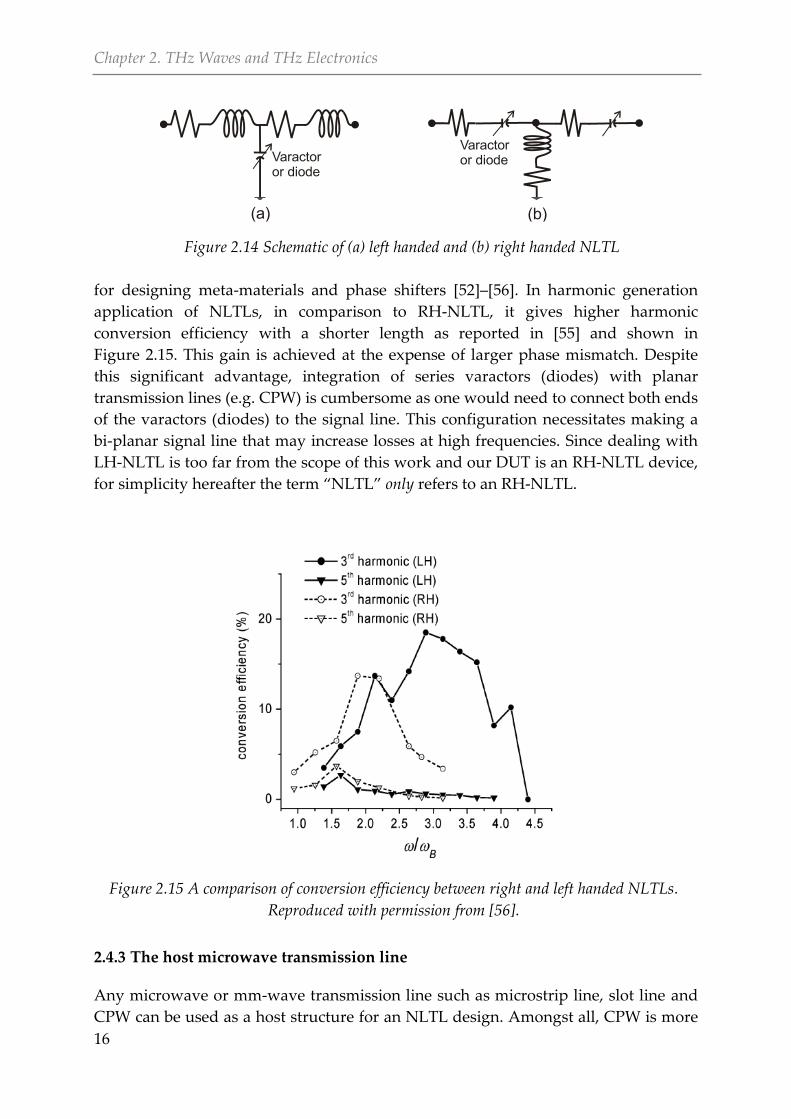
Left and right handed NLTLs 2.4.2
NLTL can be classified in either right or left handed design based on the arrangement
of varactors on the host transmission line. As shown in Figure 2.14 (a), a typical right
handed NLTL (RH-NLTL) can be illustrated by placing varactors in shunt branches
of the circuit ladder along microwave transmission line. This kind of NLTL is more
conventional and can be used for pulse shaping or as a distributed phase shifter.
In contrast to RH-NLTL, a dual design is called left-handed (LH-NLTL). In
this configuration, varactors are incorporated in series branches of the transmission
line ladder as depicted in Figure 2.14 (b). The term “left handed” is chosen since it
behaves with anomalous dispersion and negative refractive index. In an LH-NLTL,
the group and phase velocity are in the opposite direction and this property is useful
1 VFB stands for flat band voltage.
Chapter 2. THz Waves and THz Electronics
16
for designing meta-materials and phase shifters [52]–[56]. In harmonic generation
application of NLTLs, in comparison to RH-NLTL, it gives higher harmonic
conversion efficiency with a shorter length as reported in [55] and shown in
Figure 2.15. This gain is achieved at the expense of larger phase mismatch. Despite
this significant advantage, integration of series varactors (diodes) with planar
transmission lines (e.g. CPW) is cumbersome as one would need to connect both ends
of the varactors (diodes) to the signal line. This configuration necessitates making a
bi-planar signal line that may increase losses at high frequencies. Since dealing with
LH-NLTL is too far from the scope of this work and our DUT is an RH-NLTL device,
for simplicity hereafter the term “NLTL” only refers to an RH-NLTL.
The host microwave transmission line 2.4.3
Any microwave or mm-wave transmission line such as microstrip line, slot line and
CPW can be used as a host structure for an NLTL design. Amongst all, CPW is more
Figure 2.15 A comparison of conversion efficiency between right and left handed NLTLs.
Reproduced with permission from [56].
Varactoror diode
Varactoror diode
(a) (b)
Figure 2.14 Schematic of (a) left handed and (b) right handed NLTL
2.4. A short theory of NLTL and its THz range design considerations
17
convenient for design because of its quasi TEM broadband performance, more
accurate design models, less parasitic effects and radiation losses, as well as a good
compatibility with MIMICs [58]. Beside all of these advantages, it can also be
fabricated with a simpler process by only one substrate side metallization which
makes it appropriate for on-wafer probing.
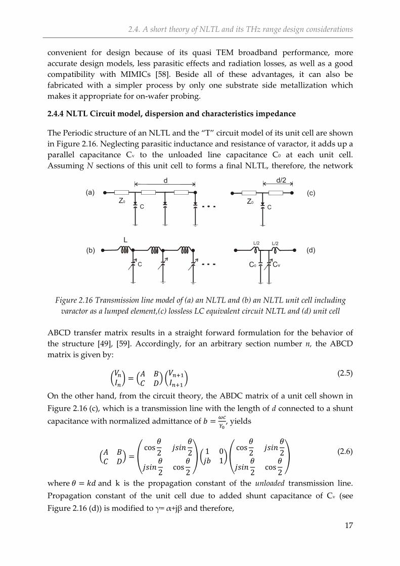
NLTL Circuit model, dispersion and characteristics impedance 2.4.4
The Periodic structure of an NLTL and the “T” circuit model of its unit cell are shown
in Figure 2.16. Neglecting parasitic inductance and resistance of varactor, it adds up a
parallel capacitance Cv to the unloaded line capacitance C0 at each unit cell.
Assuming N sections of this unit cell to forms a final NLTL, therefore, the network
ABCD transfer matrix results in a straight forward formulation for the behavior of
the structure [49], [59]. Accordingly, for an arbitrary section number n, the ABCD
matrix is given by:
(
) (
) (
)
(2.5)
On the other hand, from the circuit theory, the ABDC matrix of a unit cell shown in
Figure 2.16 (c), which is a transmission line with the length of d connected to a shunt
capacitance with normalized admittance of
, yields
(
) (
) (
)(
) (2.6)
where and k is the propagation constant of the unloaded transmission line.
Propagation constant of the unit cell due to added shunt capacitance of Cv (see
Figure 2.16 (d)) is modified to γ= α+jβ and therefore,
C
C
L/2L/2
CvC0
C
(a)
(b)
(c)
(d)
Z0 Z0
Figure 2.16 Transmission line model of (a) an NLTL and (b) an NLTL unit cell including
varactor as a lumped element,(c) lossless LC equivalent circuit NLTL and (d) unit cell
Chapter 2. THz Waves and THz Electronics
18
(
) (
)
(2.7)
By comparing to Eq. (2.5) we have
(
) (
) (
) (
)
or
(2.8)
(
) ( ) (
) (2.9)
and for a nontrivial solution, ( ) . Since in a reciprocal
network, which is a case here for a unit cell, , therefore, with substituting
Eq. (2.6) in this equation
( )
( )
( ) (2.10)
This equation, so-called dispersion relation, shows the relation between the NLTL
and the unloaded transmission line propagation constants. Assuming no losses for
the network (α=0), Eq. (2.10) leads to
( ) ( )
( ) (2.11)
On the other side, if one considers varactors as lumped elements which locally add
up a voltage dependent capacitance to the line, in a very simple approach, phase
velocity and consequently delay per-section yield
√ ( ( )) √ ( ( )) (2.12)
which shows a voltage dependency for the wave velocity and phase. Consequently,
from the transmission line theory [59], the characteristics impedance of NLTL can be
calculated as
√
( ) (2.13)
To get a feeling of the overall impedance for the NLTL, the average value of the
varactor capacitance can be used as
∫ ( )
(2.14)
where VH and VL indicate the highest and lowest voltage levels of the propagating
signal, respectively.
2.4. A short theory of NLTL and its THz range design considerations
19
Bandwidth consideration 2.4.5
NLTL1 is a lowpass structure, and its bandwidth can be drastically limited by the
technology and design. The cutoff frequency of a varactor which is a key factor in
achieving the highest frequency of the design is given by:
(2.15)
where are the diode (varactor) series resistance and capacitance
respectively. Albeit faster devices are favorable, selection of technologies such as
CMOS can make a tradeoff between cost and performance of the NLTL. Recent
progress in the high speed CMOS varactors [46] shows a cutoff frequency more than
500 GHz. However, it is still far below a multi-THz cutoff frequency of GaAs
Schottky diodes [45],[60]. Therefore, implementing an NLTL with Schottky diodes
strongly enhances its operational bandwidth, as van der Weide [61] in 1994
addressed an electrical pulse as short as 450 fs with this approach. Another obstacle
for an NLTL to reach its highest bandwidth arises from its periodic nature. Although
the distributed network of an NLTL in comparison to resonate matching networks
exhibits much more broadband behavior [48], [60] , its periodic structures can also
limit its bandwidth by the structure Bragg frequency. The term “Bragg frequency”
was suggested due to the similarity of NLTL periodic structure to periodic lattice
structures which can be characterized with X-ray. The Bragg resonant frequency [48]
of an NLTL can be defined as
√
(2.16)
which is a frequency at which the structure signal transmission (S21) reduces to zero.
In other words, at Bragg frequency, the impedance of NLTL exhibits a short circuit
behavior and beyond this frequency, the wave cannot propagate on the structure in a
normal way. The NLTL impedance with respect to the Bragg frequency [60] is given
by
√
√
(2.17)
Common applications of NLTL 2.4.6
There are lots of applications for NLTLs such as pulse compression [50], [51], soliton
and high power shock waves generation [52], [53], pulse amplification [54], phase
1 RH-NLTL since LH-NLTL is a high pass structure.
Chapter 2. THz Waves and THz Electronics
20
shifter [55], [56], frequency selectors [55], [57], and high-speed measurement systems
with sub picosecond resolution [49]. The latter has recently been demonstrated by
Anritsu® for the development of a network analyzer extension module [53], [58]. In
the following section, the mechanism of NLTL for pulse shaping and soliton
generation is described.
Shock wave generation
Shortly before, in Eq. (2.12) we saw that varactors impose a voltage-dependent phase
velocity for the traveling signal on NLTL. This unique property of NLTL is a key
factor for pulse compression or shock wave generation. The mechanism is as follows:
for a pulse which is propagating on an NLTL, the peak can travel slower (faster) than
its trough, and consequently its fall (rise) time steepens. For a signal which is
propagating on NLTL, at each section (unit cell) it receives a phase shift and step by
step becomes sharper in the edge as shown in Figure 2.17. It is worth to mention that
to enhance the Bragg frequency and achieve a shorter fall (rise) time; large
characteristics impedance for the host transmission line is required. Implementing
CPW with very high characteristics impedance with CMOS faces with technological
limitations and become unfeasible. For this reason, usually typical impedance values
between 75-100 Ω [44], [60] are acceptable. One drawback of having large impedance
for the host transmission line is its large intrinsic inductance which implicitly
produces conductive dissipations and hence, reduces the NLTL power handling
efficiency.
It should be pointed out that although for a high impedance host transmission
line, we have a mismatch with a 50 Ω loads, this can be compensated by the
capacitance of varactor itself. In other words, a part of the large inductance of the
unloaded line vanishes by the varactors capacitances.
Signal level (V)
Time (s)
section 1
θ1 θn
section n section 2
θ2
Figure 2.17 NLTL as a pulse compressor for shock wave generation. The pulse by passing
through the NLTL periodic sections becomes sharper in fall time (θn > θn-1>..>θ1). Figure
adapted by author from [48].
2.4. A short theory of NLTL and its THz range design considerations
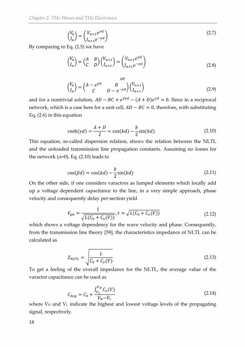
21
Theoretically, increasing the number of periodic sections N of an NLTL results
in sharper pulse, however, the skin-effect and radiation losses of CPW also hamper
this goal by decaying the amplitude of the propagating signal. Having in mind that
the radiation loss of a CPW at frequencies close to 1 THz can increase with a rate of
10 dB/mm [62], therefore the longer the line larger the decay of the voltage and
consequently resulting in less swing range for the varactor capacitances. The
dissipation due to the parasitic resistance of varactors can also act in the same way
[49]. A trade of scenario, therefore, for a designer should be incorporating many
high-performance small devices at short intervals and reducing losses by shortening
the length of NLTL. Ideally, a well-designed NLTL can only be limited in bandwidth
by the fundamental properties of the utilized varactor time constant shown in Eq.
(2.15) and the Bragg frequency.
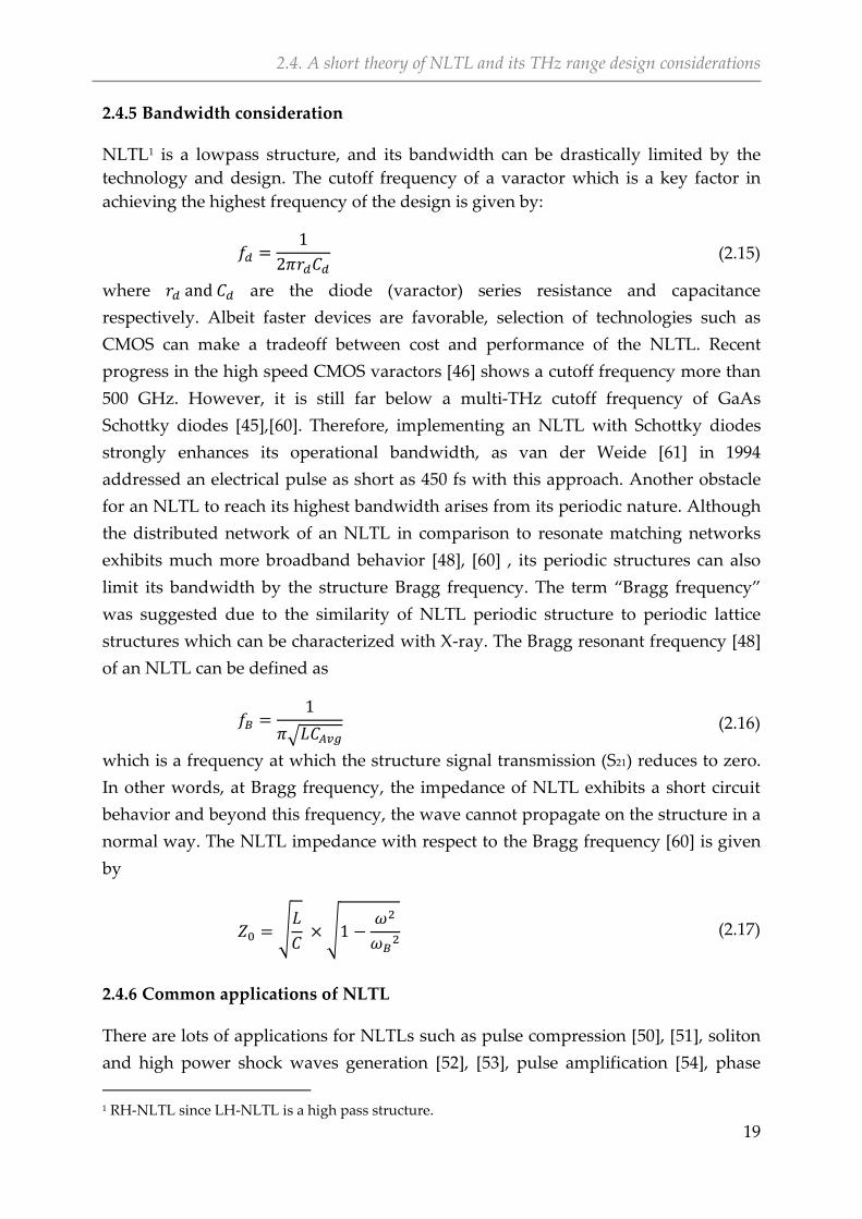
Soliton generation
The functionality and behavior of an NLTL can be expressed by its fundamental
Figure 2.18 Soliton wave generation and propagation on an NLTL. (a) the speed of soliton
depends on its amplitude, (b) mechanism showing how a soliton is generated from an input
pulse and (c) traveling of a soliton on a lossy line. Reproduced with permission from [70].
Chapter 2. THz Waves and THz Electronics
22
characteristics including dispersion (attributed to the periodicity of unit cells) and
nonlinearity of varactors. The dispersion and nonlinearity play contrary roles. For a
propagating wave on an NLTL, dispersion broadens the pulse while the nonlinearity
compresses. At the balance between these two effects, the final behavior of the
system can be identified. Much below the Bragg frequency1, NLTL shows small
dispersion which makes it appropriate for shockwave generation [60]. This regime of
operation has the highest attraction for us as our DUT is accordingly designed. By
approaching to the Bragg frequency, the NLTL behaves very dispersive and becomes
suitable for soliton generation [48], [60], [63]–[68], in which the energy of the input
pulse can be distributed over one or few decomposed pulses, resulting in a very high
amplitude pulse. Nahata et al. [69] have investigated on amplification of very short
pulses using NLTL whit this approach. An electrical soliton [70], similar to optical
frequency solitons in fiber optics, is an interaction between dispersion and
nonlinearity, as sketched in Figure 2.18. If there is no loss for an NLTL, the amplitude
of soliton can be increased orders of magnitude larger than that for the input pulse.
2.5 THz detectors and sensors
So far, common ways of generating THz waves have been mentioned, but on the
other side, the detection of THz waves with a good and highly sensitive detector
which can compensate the lack of the power of the emitter, is highly demanded.
Interestingly, many THz generators can also be utilized as detectors. However, some
changes might be needed. Photoconductive Auston switch, integrated with a THz
antenna for time domain spectroscopy (TDS) of THz detection is a good example. In
comparison to the GaAs based emitter, here the semiconductor used, must be faster
in response to the optical pulse. For this reason, materials such as low temperature
grown GaAs (Lt- GaAs), which in contrast to intrinsic GaAs indicates much less
carrier lifetime, can be used. Zheng et al. [21], with this scheme, have demonstrated
electrical transient as short as 360 fs corresponding to 1.25 THz of 3-dB bandwidth,
and a carrier lifetime of 150 fs, as well as 7% quantum efficiency.
Detecting of THz signals by means of electronics has also attracted attention.
Fortunately, since the electronic detection of THz wave works in a low power regime
[6], the power handling challenge which was already mentioned in this chapter, is
not a crucial issue. However, the new challenge here is noise reduction and
sensitivity improvement.
EOS working in a heterodyne system is another scheme of detecting of THz
waves. In this technique an electrooptic crystal senses the THz electric field based on
the Pockels effect. As will be seen later on, in next chapters of this work, this method
is highly broadband which is fully applicable for the ultrafast electronic
characterization.
1
2.5. THz detectors and sensors
23
A category of THz detectors, which is a bit far from this work, are temperature
based components like Bolometer [71]–[73], Golay cell and thermopiles. These
detectors principally absorb THz wavelengths according to black body radiation and
convert it to an electric signal. Although these THz sensors have been widely used in
THz imaging, because of their incoherent and slow response, they are inappropriate
for heterodyne applications.

25
Characterization of mm-Wave and 3.
THz Devices
In the previous chapter, the state-of-the-art electronic generation of THz waves and
more specifically NLTL approach were mentioned. Regardless of the difficulties in
making THz devices, their characterization is the next challenging issue as it requires
very high-speed instrumentation. In the range of mm-wave and THz, two main
characterization methods including electronics and photonics are used which are
discussed in this chapter.
3.1 Common electronic instrumentation
Electronic based measurement systems such as spectrum analyzer, network
analyzers and sampling oscilloscope are widely used for the characterization of high
speed devices. For the latter, there is a limitation in the temporal resolution and
spectrum analyzers only measure the power of a signal without giving information
about the phase. In contrast, Vector Network Analyzers (VNAs) are capable of
measuring both the amplitude and phase of the signal. In microwaves and millimeter
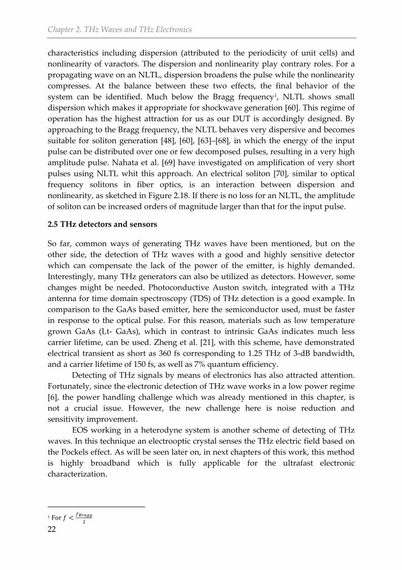
wave, the S-parameters using transmission and reflection of a signal (see Figure 3.1)
are used for the full characterization of a multiport device and in this regard VNAs
S11 S22
S21
S12
a1
b1 a2
b2
(
) (
) (
)
Figure 3.1 S-parameters of a two-port network where a and b show the incident and
reflected voltages at a port respectively.
Chapter 3. Characterization of mm-Wave and THz Devices
26
are perhaps the most appropriate electronic measurement solution. The phase
information of the S-parameters helps to figure out the behavior of devices in terms
of time delay and the phase (group) velocity. VNAs are also applicable for the
characterization of passive devices such as RF cables, filters, isolators, attenuator,
connectors, adaptors, antennas and active devices like power amplifiers and mixers.
To date, most of modern VNAs can characterize devices in a frequency range
up to 70 GHz [1], [74], [75]. The problem emerges when a DUT works at higher
frequencies where we need faster internal components inside the instruments.
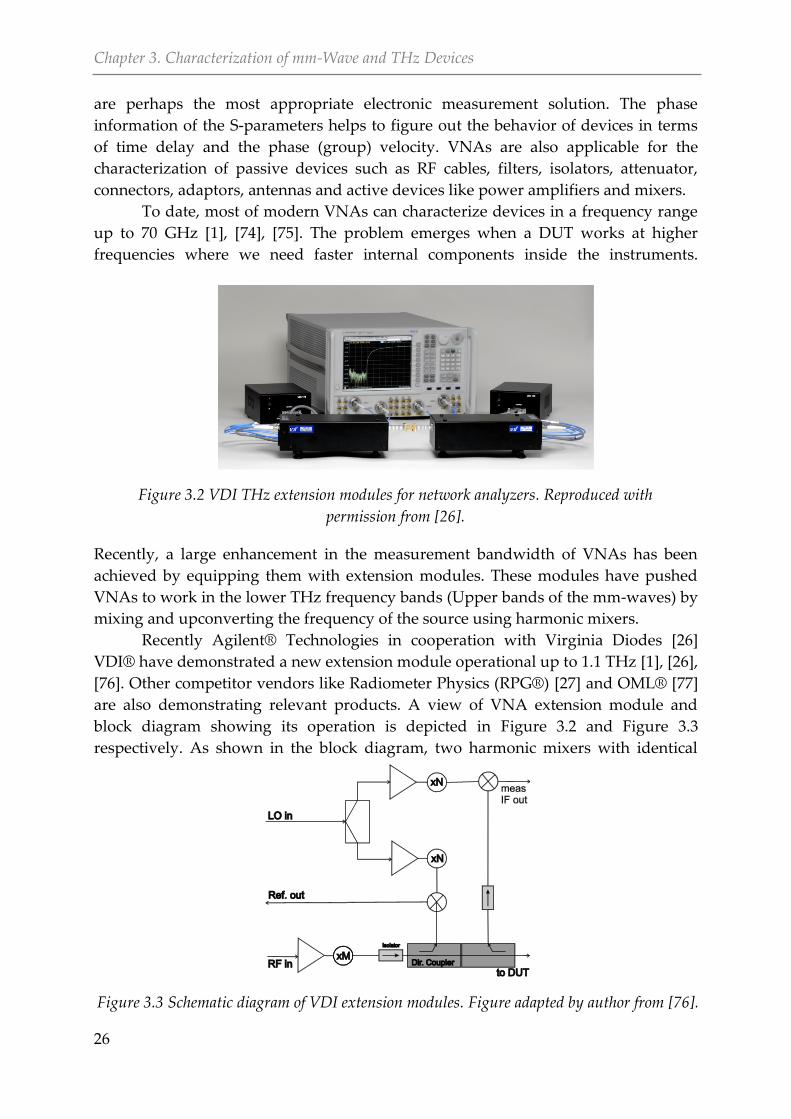
Recently, a large enhancement in the measurement bandwidth of VNAs has been
achieved by equipping them with extension modules. These modules have pushed
VNAs to work in the lower THz frequency bands (Upper bands of the mm-waves) by
mixing and upconverting the frequency of the source using harmonic mixers.
Recently Agilent® Technologies in cooperation with Virginia Diodes [26]
VDI® have demonstrated a new extension module operational up to 1.1 THz [1], [26],
[76]. Other competitor vendors like Radiometer Physics (RPG®) [27] and OML® [77]
are also demonstrating relevant products. A view of VNA extension module and
block diagram showing its operation is depicted in Figure 3.2 and Figure 3.3
respectively. As shown in the block diagram, two harmonic mixers with identical
Figure 3.2 VDI THz extension modules for network analyzers. Reproduced with
permission from [26].
Figure 3.3 Schematic diagram of VDI extension modules. Figure adapted by author from [76].
3.1. Common electronic instrumentation
27
functionalities are used to upconvert the signal of the generator in the transmitter
side, and simultaneously downconvert the RF response of the DUT in the receiver.
The system is configured as a heterodyne detector with RF, LO and IF and the signal
is finally translated to an IF for signal processing and S-parameters analysis. In the
following sections the features and functionalities of the extension modules from
Virginia diodes®, combined with a VNA from Agilent® as a cutting edge technology
in the THz electronic characterization, are introduced.
Table 3.1 Standard waveguide bands for mm-wave and THz range. Source from [78]. Military name IEEE name Frequency range (GHz)
WR-15 WM-3759 50–75
WR-12 WM-3099 60–90
WR-10 WM-2540 75–110
WR-08 WM-2032 90–140
WR-06 WM-1651 110–170
WR-05 WM-1295 140–220
WR-04 WM-1092 170–260
WR-03 WM-864 220–330
WR-02 WM-570 330–500
WR-1.5 WM-380 500–750
WR-1.0 WM-250 750–1100
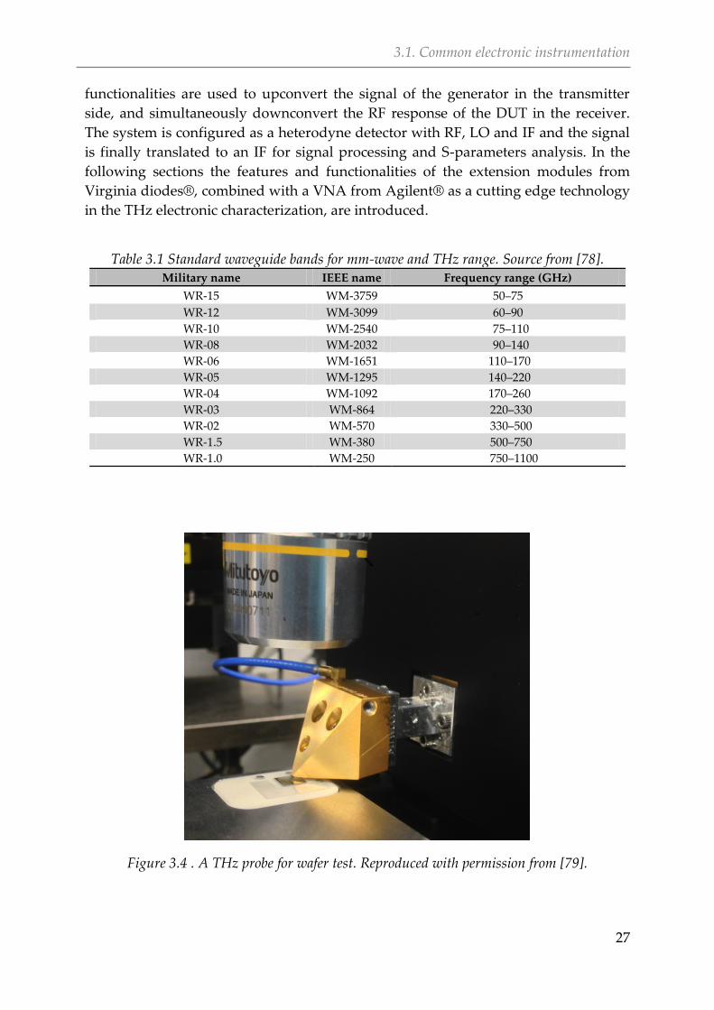
Figure 3.4 . A THz probe for wafer test. Reproduced with permission from [79].
Chapter 3. Characterization of mm-Wave and THz Devices
28
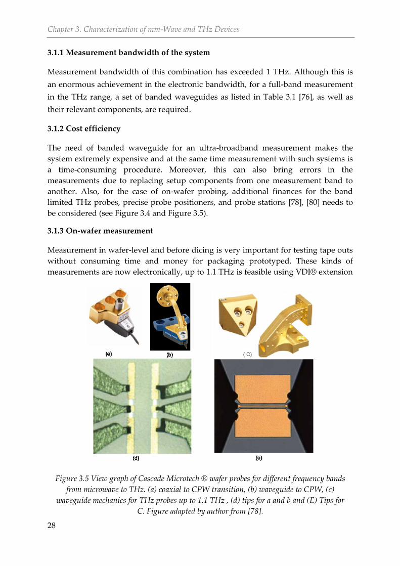
Figure 3.5 View graph of Cascade Microtech ® wafer probes for different frequency bands
from microwave to THz. (a) coaxial to CPW transition, (b) waveguide to CPW, (c)
waveguide mechanics for THz probes up to 1.1 THz , (d) tips for a and b and (E) Tips for
C. Figure adapted by author from [78].
Measurement bandwidth of the system 3.1.1
Measurement bandwidth of this combination has exceeded 1 THz. Although this is
an enormous achievement in the electronic bandwidth, for a full-band measurement
in the THz range, a set of banded waveguides as listed in Table 3.1 [76], as well as
their relevant components, are required.
Cost efficiency 3.1.2
The need of banded waveguide for an ultra-broadband measurement makes the
system extremely expensive and at the same time measurement with such systems is
a time-consuming procedure. Moreover, this can also bring errors in the
measurements due to replacing setup components from one measurement band to
another. Also, for the case of on-wafer probing, additional finances for the band
limited THz probes, precise probe positioners, and probe stations [78], [80] needs to
be considered (see Figure 3.4 and Figure 3.5).
On-wafer measurement 3.1.3
Measurement in wafer-level and before dicing is very important for testing tape outs
without consuming time and money for packaging prototyped. These kinds of
measurements are now electronically, up to 1.1 THz is feasible using VDI® extension
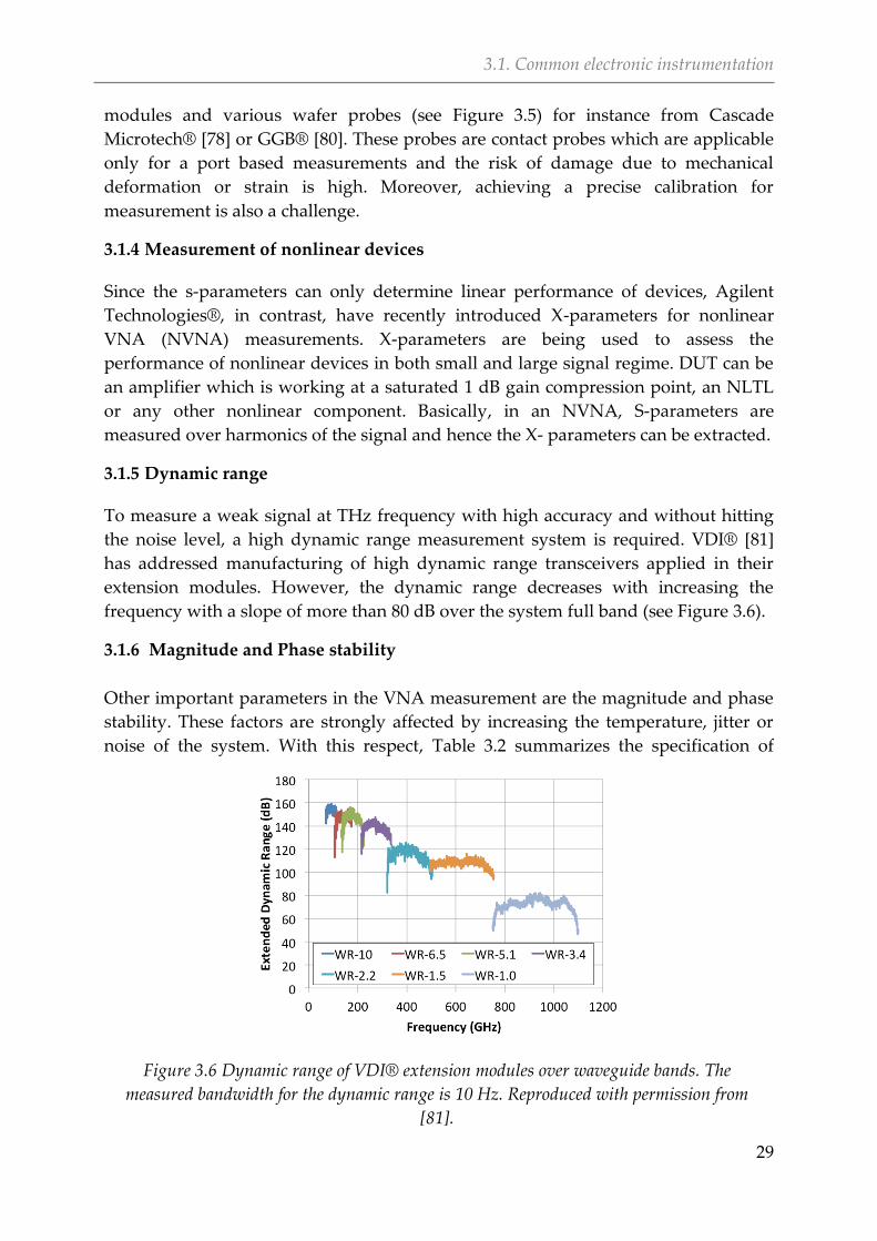
3.1. Common electronic instrumentation
29
modules and various wafer probes (see Figure 3.5) for instance from Cascade
Microtech® [78] or GGB® [80]. These probes are contact probes which are applicable
only for a port based measurements and the risk of damage due to mechanical
deformation or strain is high. Moreover, achieving a precise calibration for
measurement is also a challenge.
Measurement of nonlinear devices 3.1.4
Since the s-parameters can only determine linear performance of devices, Agilent
Technologies®, in contrast, have recently introduced X-parameters for nonlinear
VNA (NVNA) measurements. X-parameters are being used to assess the
performance of nonlinear devices in both small and large signal regime. DUT can be
an amplifier which is working at a saturated 1 dB gain compression point, an NLTL
or any other nonlinear component. Basically, in an NVNA, S-parameters are
measured over harmonics of the signal and hence the X- parameters can be extracted.
Dynamic range 3.1.5
To measure a weak signal at THz frequency with high accuracy and without hitting
the noise level, a high dynamic range measurement system is required. VDI® [81]
has addressed manufacturing of high dynamic range transceivers applied in their
extension modules. However, the dynamic range decreases with increasing the
frequency with a slope of more than 80 dB over the system full band (see Figure 3.6).
Magnitude and Phase stability 3.1.6
Other important parameters in the VNA measurement are the magnitude and phase
stability. These factors are strongly affected by increasing the temperature, jitter or
noise of the system. With this respect, Table 3.2 summarizes the specification of
Figure 3.6 Dynamic range of VDI® extension modules over waveguide bands. The
measured bandwidth for the dynamic range is 10 Hz. Reproduced with permission from
[81].
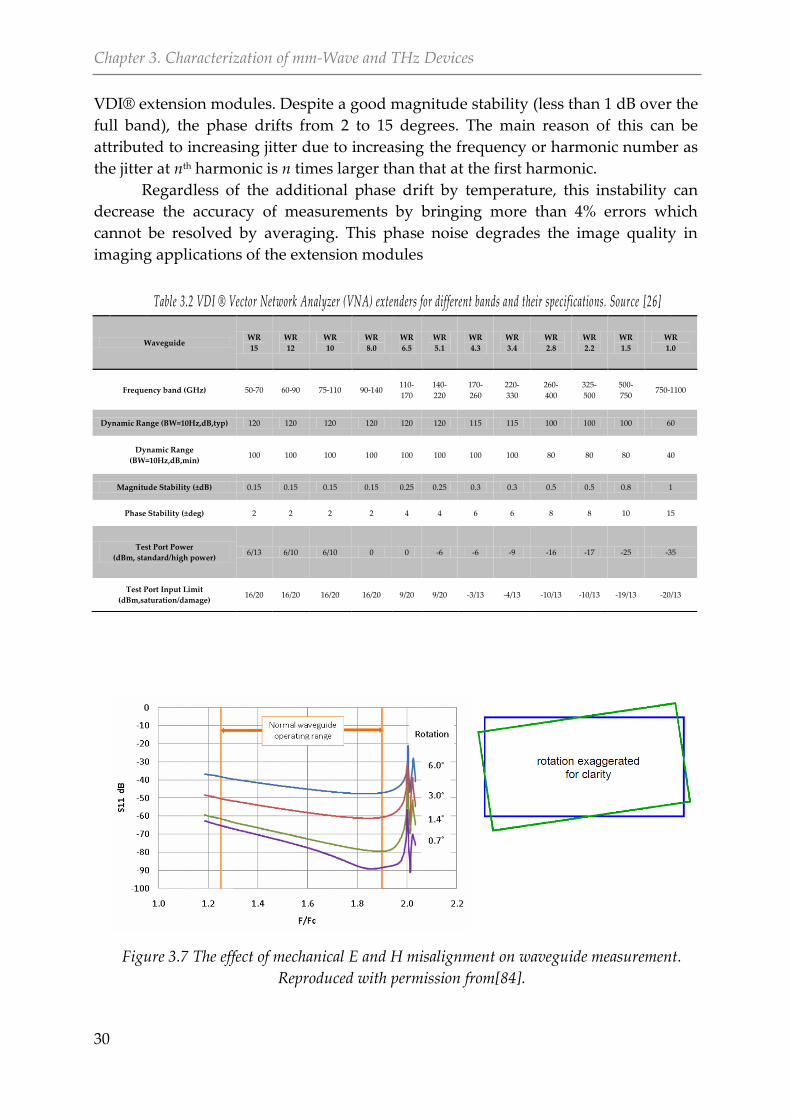
Chapter 3. Characterization of mm-Wave and THz Devices
30
VDI® extension modules. Despite a good magnitude stability (less than 1 dB over the
full band), the phase drifts from 2 to 15 degrees. The main reason of this can be
attributed to increasing jitter due to increasing the frequency or harmonic number as
the jitter at nth harmonic is n times larger than that at the first harmonic.
Regardless of the additional phase drift by temperature, this instability can
decrease the accuracy of measurements by bringing more than 4% errors which
cannot be resolved by averaging. This phase noise degrades the image quality in
imaging applications of the extension modules
Table 3.2 VDI ® Vector Network Analyzer (VNA) extenders for different bands and their specifications. Source [26]
Waveguide WR
15
WR
12
WR
10
WR
8.0
WR
6.5
WR
5.1
WR
4.3
WR
3.4
WR
2.8
WR
2.2
WR
1.5
WR
1.0
Frequency band (GHz) 50-70 60-90 75-110 90-140 110-
170
140-
220
170-
260
220-
330
260-
400
325-
500
500-
750 750-1100
Dynamic Range (BW=10Hz,dB,typ) 120 120 120 120 120 120 115 115 100 100 100 60
Dynamic Range
(BW=10Hz,dB,min) 100 100 100 100 100 100 100 100 80 80 80 40
Magnitude Stability (±dB) 0.15 0.15 0.15 0.15 0.25 0.25 0.3 0.3 0.5 0.5 0.8 1
Phase Stability (±deg) 2 2 2 2 4 4 6 6 8 8 10 15
Test Port Power
(dBm, standard/high power) 6/13 6/10 6/10 0 0 -6 -6 -9 -16 -17 -25 -35
Test Port Input Limit
(dBm,saturation/damage) 16/20 16/20 16/20 16/20 9/20 9/20 -3/13 -4/13 -10/13 -10/13 -19/13 -20/13
Figure 3.7 The effect of mechanical E and H misalignment on waveguide measurement.
Reproduced with permission from[84].
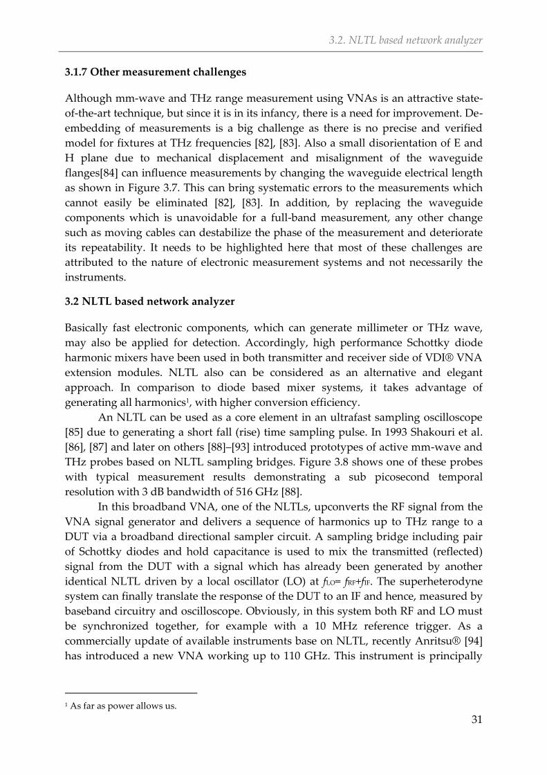
3.2. NLTL based network analyzer
31
Other measurement challenges 3.1.7
Although mm-wave and THz range measurement using VNAs is an attractive state-
of-the-art technique, but since it is in its infancy, there is a need for improvement. De-
embedding of measurements is a big challenge as there is no precise and verified
model for fixtures at THz frequencies [82], [83]. Also a small disorientation of E and
H plane due to mechanical displacement and misalignment of the waveguide
flanges[84] can influence measurements by changing the waveguide electrical length
as shown in Figure 3.7. This can bring systematic errors to the measurements which
cannot easily be eliminated [82], [83]. In addition, by replacing the waveguide
components which is unavoidable for a full-band measurement, any other change
such as moving cables can destabilize the phase of the measurement and deteriorate
its repeatability. It needs to be highlighted here that most of these challenges are
attributed to the nature of electronic measurement systems and not necessarily the
instruments.
3.2 NLTL based network analyzer
Basically fast electronic components, which can generate millimeter or THz wave,
may also be applied for detection. Accordingly, high performance Schottky diode
harmonic mixers have been used in both transmitter and receiver side of VDI® VNA
extension modules. NLTL also can be considered as an alternative and elegant
approach. In comparison to diode based mixer systems, it takes advantage of
generating all harmonics1, with higher conversion efficiency.
An NLTL can be used as a core element in an ultrafast sampling oscilloscope
[85] due to generating a short fall (rise) time sampling pulse. In 1993 Shakouri et al.
[86], [87] and later on others [88]–[93] introduced prototypes of active mm-wave and
THz probes based on NLTL sampling bridges. Figure 3.8 shows one of these probes
with typical measurement results demonstrating a sub picosecond temporal
resolution with 3 dB bandwidth of 516 GHz [88].
In this broadband VNA, one of the NLTLs, upconverts the RF signal from the
VNA signal generator and delivers a sequence of harmonics up to THz range to a
DUT via a broadband directional sampler circuit. A sampling bridge including pair
of Schottky diodes and hold capacitance is used to mix the transmitted (reflected)
signal from the DUT with a signal which has already been generated by another
identical NLTL driven by a local oscillator (LO) at fLO= fRF+fIF. The superheterodyne
system can finally translate the response of the DUT to an IF and hence, measured by
baseband circuitry and oscilloscope. Obviously, in this system both RF and LO must
be synchronized together, for example with a 10 MHz reference trigger. As a
commercially update of available instruments base on NLTL, recently Anritsu® [94]
has introduced a new VNA working up to 110 GHz. This instrument is principally
1 As far as power allows us.
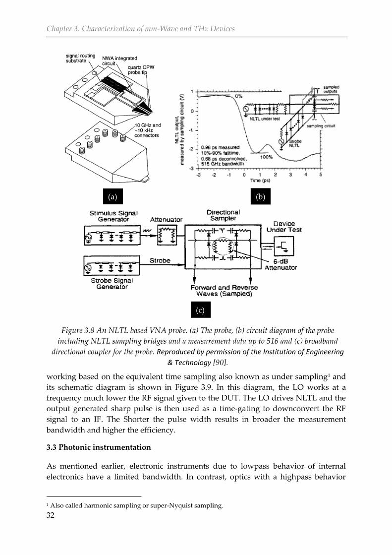
Chapter 3. Characterization of mm-Wave and THz Devices
32
working based on the equivalent time sampling also known as under sampling1 and
its schematic diagram is shown in Figure 3.9. In this diagram, the LO works at a
frequency much lower the RF signal given to the DUT. The LO drives NLTL and the
output generated sharp pulse is then used as a time-gating to downconvert the RF
signal to an IF. The Shorter the pulse width results in broader the measurement
bandwidth and higher the efficiency.
3.3 Photonic instrumentation
As mentioned earlier, electronic instruments due to lowpass behavior of internal
electronics have a limited bandwidth. In contrast, optics with a highpass behavior
1 Also called harmonic sampling or super-Nyquist sampling.
(a) (b)
(c)
Figure 3.8 An NLTL based VNA probe. (a) The probe, (b) circuit diagram of the probe
including NLTL sampling bridges and a measurement data up to 516 and (c) broadband
directional coupler for the probe. Reproduced by permission of the Institution of Engineering
& Technology [90].
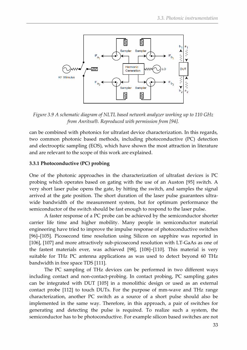
3.3. Photonic instrumentation
33
can be combined with photonics for ultrafast device characterization. In this regards,
two common photonic based methods, including photoconductive (PC) detection
and electrooptic sampling (EOS), which have shown the most attraction in literature
and are relevant to the scope of this work are explained.
Photoconductive (PC) probing 3.3.1
One of the photonic approaches in the characterization of ultrafast devices is PC
probing which operates based on gating with the use of an Auston [95] switch. A
very short laser pulse opens the gate, by hitting the switch, and samples the signal
arrived at the gate position. The short duration of the laser pulse guarantees ultra-
wide bandwidth of the measurement system, but for optimum performance the
semiconductor of the switch should be fast enough to respond to the laser pulse.
A faster response of a PC probe can be achieved by the semiconductor shorter
carrier life time and higher mobility. Many people in semiconductor material
engineering have tried to improve the impulse response of photoconductive switches
[96]–[105]. Picosecond time resolution using Silicon on sapphire was reported in
[106], [107] and more attractively sub-picosecond resolution with LT-GaAs as one of
the fastest materials ever, was achieved [98], [108]–[110]. This material is very
suitable for THz PC antenna applications as was used to detect beyond 60 THz
bandwidth in free space TDS [111].
The PC sampling of THz devices can be performed in two different ways
including contact and non-contact-probing. In contact probing, PC sampling gates
can be integrated with DUT [105] in a monolithic design or used as an external
contact probe [112] to touch DUTs. For the purpose of mm-wave and THz range
characterization, another PC switch as a source of a short pulse should also be
implemented in the same way. Therefore, in this approach, a pair of switches for
generating and detecting the pulse is required. To realize such a system, the
semiconductor has to be photoconductive. For example silicon based switches are not
Figure 3.9 A schematic diagram of NLTL based network analyzer working up to 110 GHz
from Anritsu®. Reproduced with permission from [94].
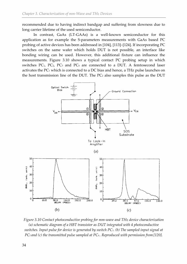
Chapter 3. Characterization of mm-Wave and THz Devices
34
recommended due to having indirect bandgap and suffering from slowness due to
long carrier lifetime of the used semiconductor.
In contrast, GaAs (LT-GAAs) is a well-known semiconductor for this
application as for example the S-parameters measurements with GaAs based PC
probing of active devices has been addressed in [104], [113]–[124]. If incorporating PC
switches on the same wafer which holds DUT is not possible, an interface like
bonding wiring can be used. However, this additional fixture can influence the
measurements. Figure 3.10 shows a typical contact PC probing setup in which
switches PC1, PC2, PC3 and PC4 are connected to a DUT. A femtosecond laser
activates the PC1 which is connected to a DC bias and hence, a THz pulse launches on
the host transmission line of the DUT. The PC2 also samples this pulse as the DUT
(a)
(c) (b)
Figure 3.10 Contact photoconductive probing for mm-wave and THz device characterization
(a) schematic diagram of a HBT transistor as DUT integrated with 4 photoconductive
switches. Input pulse for device is generated by switch PC1. (b) The sampled input signal at
PC2 and (c) the transmitted pulse sampled at PC4.. Reproduced with permission from [120].
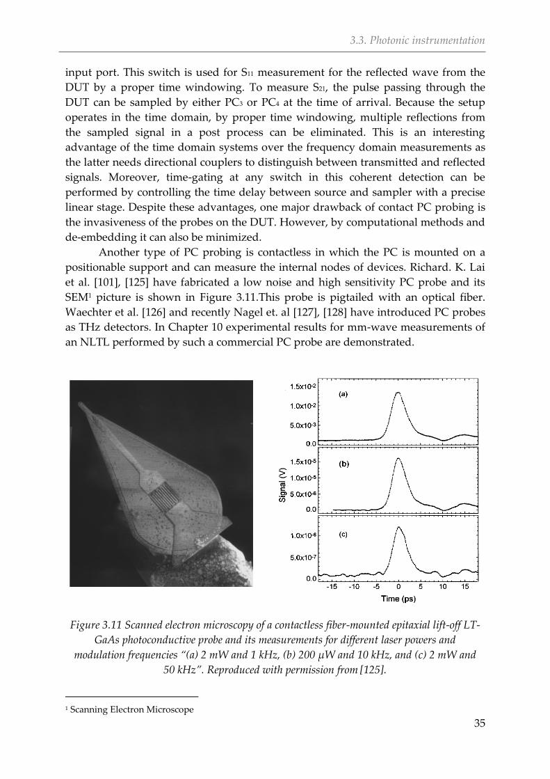
3.3. Photonic instrumentation
35
input port. This switch is used for S11 measurement for the reflected wave from the
DUT by a proper time windowing. To measure S21, the pulse passing through the
DUT can be sampled by either PC3 or PC4 at the time of arrival. Because the setup
operates in the time domain, by proper time windowing, multiple reflections from
the sampled signal in a post process can be eliminated. This is an interesting
advantage of the time domain systems over the frequency domain measurements as
the latter needs directional couplers to distinguish between transmitted and reflected
signals. Moreover, time-gating at any switch in this coherent detection can be
performed by controlling the time delay between source and sampler with a precise
linear stage. Despite these advantages, one major drawback of contact PC probing is
the invasiveness of the probes on the DUT. However, by computational methods and
de-embedding it can also be minimized.
Another type of PC probing is contactless in which the PC is mounted on a
positionable support and can measure the internal nodes of devices. Richard. K. Lai
et al. [101], [125] have fabricated a low noise and high sensitivity PC probe and its
SEM1 picture is shown in Figure 3.11.This probe is pigtailed with an optical fiber.
Waechter et al. [126] and recently Nagel et. al [127], [128] have introduced PC probes
as THz detectors. In Chapter 10 experimental results for mm-wave measurements of
an NLTL performed by such a commercial PC probe are demonstrated.
1 Scanning Electron Microscope
Figure 3.11 Scanned electron microscopy of a contactless fiber-mounted epitaxial lift-off LT-
GaAs photoconductive probe and its measurements for different laser powers and
modulation frequencies “(a) 2 mW and 1 kHz, (b) 200 μW and 10 kHz, and (c) 2 mW and
50 kHz”. Reproduced with permission from [125].
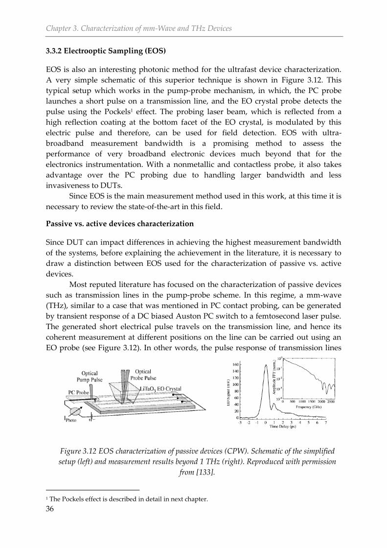
Chapter 3. Characterization of mm-Wave and THz Devices
36
Electrooptic Sampling (EOS) 3.3.2
EOS is also an interesting photonic method for the ultrafast device characterization.
A very simple schematic of this superior technique is shown in Figure 3.12. This
typical setup which works in the pump-probe mechanism, in which, the PC probe
launches a short pulse on a transmission line, and the EO crystal probe detects the
pulse using the Pockels1 effect. The probing laser beam, which is reflected from a
high reflection coating at the bottom facet of the EO crystal, is modulated by this
electric pulse and therefore, can be used for field detection. EOS with ultra-
broadband measurement bandwidth is a promising method to assess the
performance of very broadband electronic devices much beyond that for the
electronics instrumentation. With a nonmetallic and contactless probe, it also takes
advantage over the PC probing due to handling larger bandwidth and less
invasiveness to DUTs.
Since EOS is the main measurement method used in this work, at this time it is
necessary to review the state-of-the-art in this field.
Passive vs. active devices characterization
Since DUT can impact differences in achieving the highest measurement bandwidth
of the systems, before explaining the achievement in the literature, it is necessary to
draw a distinction between EOS used for the characterization of passive vs. active
devices.
Most reputed literature has focused on the characterization of passive devices
such as transmission lines in the pump-probe scheme. In this regime, a mm-wave
(THz), similar to a case that was mentioned in PC contact probing, can be generated
by transient response of a DC biased Auston PC switch to a femtosecond laser pulse.
The generated short electrical pulse travels on the transmission line, and hence its
coherent measurement at different positions on the line can be carried out using an
EO probe (see Figure 3.12). In other words, the pulse response of transmission lines
1 The Pockels effect is described in detail in next chapter.
Figure 3.12 EOS characterization of passive devices (CPW). Schematic of the simplified
setup (left) and measurement results beyond 1 THz (right). Reproduced with permission
from [133].
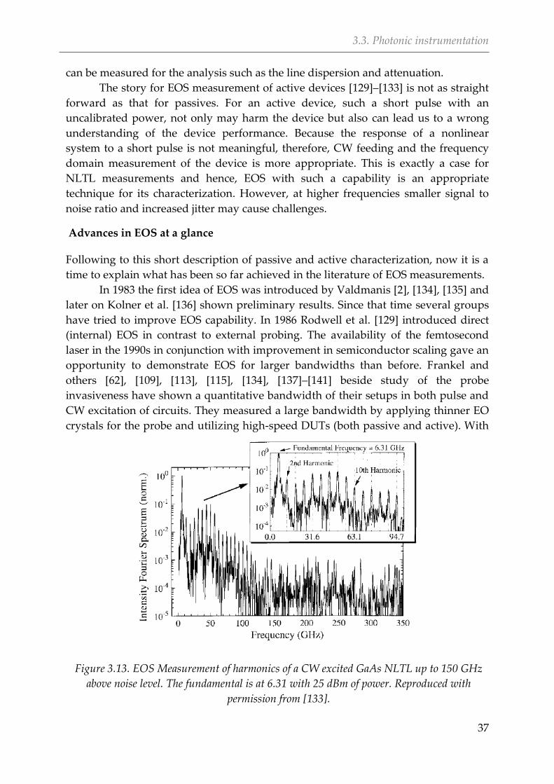
3.3. Photonic instrumentation
37
can be measured for the analysis such as the line dispersion and attenuation.
The story for EOS measurement of active devices [129]–[133] is not as straight
forward as that for passives. For an active device, such a short pulse with an
uncalibrated power, not only may harm the device but also can lead us to a wrong
understanding of the device performance. Because the response of a nonlinear
system to a short pulse is not meaningful, therefore, CW feeding and the frequency
domain measurement of the device is more appropriate. This is exactly a case for
NLTL measurements and hence, EOS with such a capability is an appropriate
technique for its characterization. However, at higher frequencies smaller signal to
noise ratio and increased jitter may cause challenges.
Advances in EOS at a glance
Following to this short description of passive and active characterization, now it is a
time to explain what has been so far achieved in the literature of EOS measurements.
In 1983 the first idea of EOS was introduced by Valdmanis [2], [134], [135] and
later on Kolner et al. [136] shown preliminary results. Since that time several groups
have tried to improve EOS capability. In 1986 Rodwell et al. [129] introduced direct
(internal) EOS in contrast to external probing. The availability of the femtosecond
laser in the 1990s in conjunction with improvement in semiconductor scaling gave an
opportunity to demonstrate EOS for larger bandwidths than before. Frankel and
others [62], [109], [113], [115], [134], [137]–[141] beside study of the probe
invasiveness have shown a quantitative bandwidth of their setups in both pulse and
CW excitation of circuits. They measured a large bandwidth by applying thinner EO
crystals for the probe and utilizing high-speed DUTs (both passive and active). With
Figure 3.13. EOS Measurement of harmonics of a CW excited GaAs NLTL up to 150 GHz
above noise level. The fundamental is at 6.31 with 25 dBm of power. Reproduced with
permission from [133].
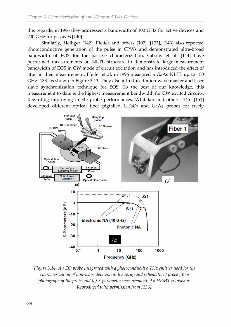
Chapter 3. Characterization of mm-Wave and THz Devices
38
this regards, in 1996 they addressed a bandwidth of 100 GHz for active devices and
700 GHz for passives [140].
Similarly, Heiliger [142], Pfeifer and others [107], [133], [143] also reported
photoconductive generation of the pulse in CPWs and demonstrated ultra-broad
bandwidth of EOS for the passive characterization. Gibony et al. [144] have
performed measurements on NLTL structure to demonstrate large measurement
bandwidth of EOS in CW mode of circuit excitation and has introduced the effect of
jitter in their measurement. Pfeifer et al. in 1996 measured a GaAs NLTL up to 150
GHz [133] as shown in Figure 3.13. They also introduced microwave master and laser
slave synchronization technique for EOS. To the best of our knowledge, this
measurement to date is the highest measurement bandwidth for CW excited circuits.
Regarding improving in EO probe performances, Whitaker and others [145]–[151]
developed different optical fiber pigtailed LiTaO3 and GaAs probes for freely
(c)
(b)
Figure 3.14. An EO probe integrated with a photoconductive THz emitter used for the
characterization of mm-wave devices. (a) the setup and schematic of probe ,(b) a
photograph of the probe and (c) S-parameter measurement of a HEMT transistor.
Reproduced with permission from [156].
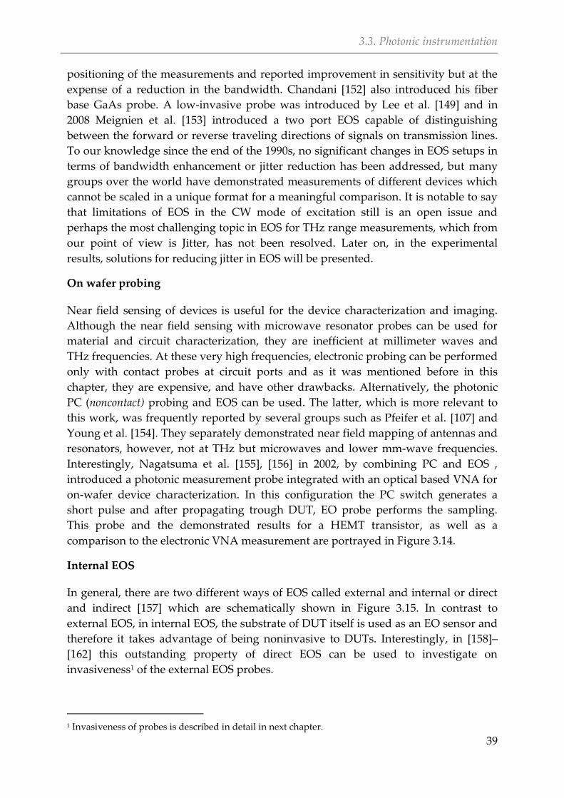
3.3. Photonic instrumentation
39
positioning of the measurements and reported improvement in sensitivity but at the
expense of a reduction in the bandwidth. Chandani [152] also introduced his fiber
base GaAs probe. A low-invasive probe was introduced by Lee et al. [149] and in
2008 Meignien et al. [153] introduced a two port EOS capable of distinguishing
between the forward or reverse traveling directions of signals on transmission lines.
To our knowledge since the end of the 1990s, no significant changes in EOS setups in
terms of bandwidth enhancement or jitter reduction has been addressed, but many
groups over the world have demonstrated measurements of different devices which
cannot be scaled in a unique format for a meaningful comparison. It is notable to say
that limitations of EOS in the CW mode of excitation still is an open issue and
perhaps the most challenging topic in EOS for THz range measurements, which from
our point of view is Jitter, has not been resolved. Later on, in the experimental
results, solutions for reducing jitter in EOS will be presented.
On wafer probing
Near field sensing of devices is useful for the device characterization and imaging.
Although the near field sensing with microwave resonator probes can be used for
material and circuit characterization, they are inefficient at millimeter waves and
THz frequencies. At these very high frequencies, electronic probing can be performed
only with contact probes at circuit ports and as it was mentioned before in this
chapter, they are expensive, and have other drawbacks. Alternatively, the photonic
PC (noncontact) probing and EOS can be used. The latter, which is more relevant to
this work, was frequently reported by several groups such as Pfeifer et al. [107] and
Young et al. [154]. They separately demonstrated near field mapping of antennas and
resonators, however, not at THz but microwaves and lower mm-wave frequencies.
Interestingly, Nagatsuma et al. [155], [156] in 2002, by combining PC and EOS ,
introduced a photonic measurement probe integrated with an optical based VNA for
on-wafer device characterization. In this configuration the PC switch generates a
short pulse and after propagating trough DUT, EO probe performs the sampling.
This probe and the demonstrated results for a HEMT transistor, as well as a
comparison to the electronic VNA measurement are portrayed in Figure 3.14.
Internal EOS
In general, there are two different ways of EOS called external and internal or direct
and indirect [157] which are schematically shown in Figure 3.15. In contrast to
external EOS, in internal EOS, the substrate of DUT itself is used as an EO sensor and
therefore it takes advantage of being noninvasive to DUTs. Interestingly, in [158]–
[162] this outstanding property of direct EOS can be used to investigate on
invasiveness1 of the external EOS probes.
1 Invasiveness of probes is described in detail in next chapter.
Chapter 3. Characterization of mm-Wave and THz Devices
40
Despite this big advantage, the direct method suffers from several
disadvantages as follows:
It necessitates using EO substrate for DUTs. This drawback excludes
silicon based circuits to be measured. However, it privileges GaAs
based devices.
Characterization of DUTs in the Pump–probe system needs two
different wavelengths for pump and probe as shown in Figure 3.15. In
this case, the wavelength of the pump beam must be smaller than the
bandgap of GaAs (850 nm) to be able to generate carriers in the
substrate, while at the same time the probe must be tuned to a
wavelength larger than this bandgap. Two different wavelengths from
a single laser source can be obtained using nonlinear optics at the cost
of more complexities.
The last but not least disadvantage of internal EOS is that the laser has
to be reflected from the metallic parts of the DUT and the field at the
gaps cannot be measured properly. It should be noted that this is a
contrast to the external probing in which a high reflection dielectric
layer at the bottom facet of the probe is used. Also, the accuracy of
measurements can be affected by the Fabry-Pérot etalon resonance of
the substrate for the probe beam.
Far Field Sensing
Mostly in this chapter the focus was on EOS for near field detecting and device
characterization, in which electrooptic probe approaches devices. It is noteworthy to
mention that EOS can also be used for far field measurements like in a TDS. In
contrast to near filed, it detects the field component of a plane wave which is
transmitted from an antenna.
Figure 3.15 (a) Indirect and (b) direct electrooptic sampling. Direct pump –probe EOS
needs two laser wavelengths λ0 and λ1.
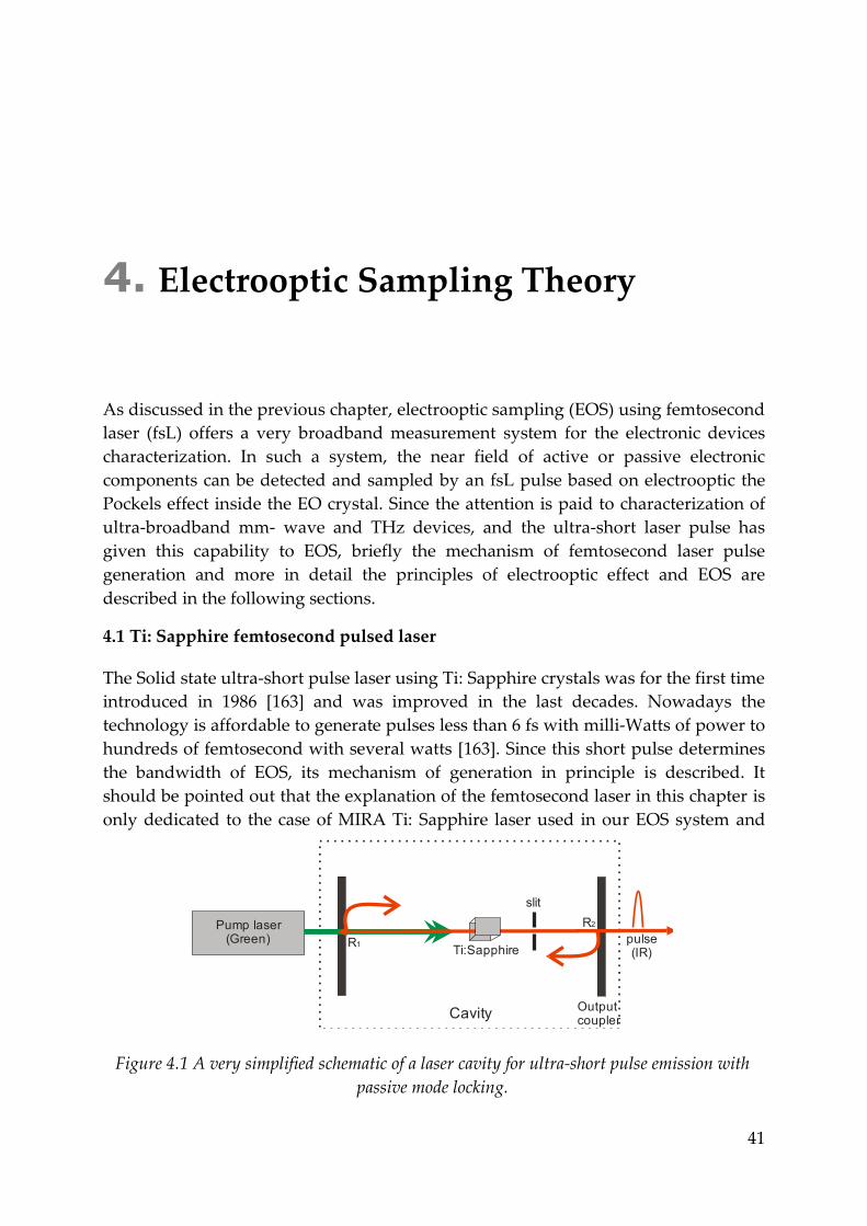
41
Electrooptic Sampling Theory 4.
As discussed in the previous chapter, electrooptic sampling (EOS) using femtosecond
laser (fsL) offers a very broadband measurement system for the electronic devices
characterization. In such a system, the near field of active or passive electronic
components can be detected and sampled by an fsL pulse based on electrooptic the
Pockels effect inside the EO crystal. Since the attention is paid to characterization of
ultra-broadband mm- wave and THz devices, and the ultra-short laser pulse has
given this capability to EOS, briefly the mechanism of femtosecond laser pulse
generation and more in detail the principles of electrooptic effect and EOS are
described in the following sections.
4.1 Ti: Sapphire femtosecond pulsed laser
The Solid state ultra-short pulse laser using Ti: Sapphire crystals was for the first time
introduced in 1986 [163] and was improved in the last decades. Nowadays the
technology is affordable to generate pulses less than 6 fs with milli-Watts of power to
hundreds of femtosecond with several watts [163]. Since this short pulse determines
the bandwidth of EOS, its mechanism of generation in principle is described. It
should be pointed out that the explanation of the femtosecond laser in this chapter is
only dedicated to the case of MIRA Ti: Sapphire laser used in our EOS system and
slit
Ti:Sapphire
Output coupler
Pump laser(Green)
Cavity
pulse(IR)
R1
R2
Figure 4.1 A very simplified schematic of a laser cavity for ultra-short pulse emission with
passive mode locking.
Chapter 4. Electrooptic Sampling Theory
42
necessarily should not be extrapolated to any other fsL.
As depicted in Figure 4.1, to generate a femtosecond pulse a cavity with a gain
media is needed. Gain media inside the cavity is required to compensate losses, and
to have a non-damping resonance for the optical beam. Ti: Sapphire (Ti3+ :Al2O3) is a
crystal which is commercially available and has been used as gain medium for fsLs.
The crystal is mechanically very stable and can tolerate very high temperature up to
20400C. It can absorb photons at 400-600 nm and perform the florescence
amplification from 680 nm-1100 nm with a maximum intensity peak at 800 nm [164].
In the absence of the pump laser (normal condition), atoms of the crystal are
stabilized in their low energy state and by absorbing photons from a pump laser,
they get excited to energetic state and stimulate or emit light. Under this
circumstance, they amplify the light instead of absorption and therefore the gain
medium is formed. The mirrors are used for the cavity bouncing and a birefringence
filter (BRF)1 can restrict the wavelength of operation. A pair of prisms1 inside the
cavity can be used to compensate group velocity dispersion of ultra-short pulse as it
passes through optical components. The laser runs in the CW mode and longitudinal
modes start lasing when the cavity length becomes exactly an integral number of the
emitted light half-wavelength i.e. L= nλ/2, where L is the half-length of the cavity.
Since n is not strictly defined, many different wavelengths can resonate coherently as
modes of the cavity. In the mode-locked state, a short pulse of the light bounces back
and forth inside the cavity and a small fraction of the light escapes from the output
coupler which is in principle a partially transparent mirror (see Figure 4.1). The
cavity round trip length 2L defines the laser repetition rate given by: f= c/2L where c
is the velocity of light in the free space. For the Mira laser the nominal repetition rate
is around 76 MHz that can be tuned in the range of ±1 MHz by changing the cavity
length with the internal mirrors. It is worth to notify that the repetition rates up to 77
GHz with few millimeter cavity length is achievable with ND:YVO4 laser [165].
Whenever the modes are fully locked, a very short pulse starts to emit.
The mode locking mechanism can be implemented in both passive and active
ways, but the active mode locking usually generates longer pulse width and needs
external electronic circuitry and synchronization [163]. In this way, the optical shutter
is controlled by electronics and opens up at the arrival time of the pulse to the gain
medium and closes again. The timing between electronic and the optical pulse must
be precisely matched to have a short pulse [163]. In other words, the modulating
frequency must be accurately set equal to the laser repetition rate. Since the length of
the cavity can slightly vary with the temperature, the electronic precise follow-up
1 Not shown in Figure 4.1.
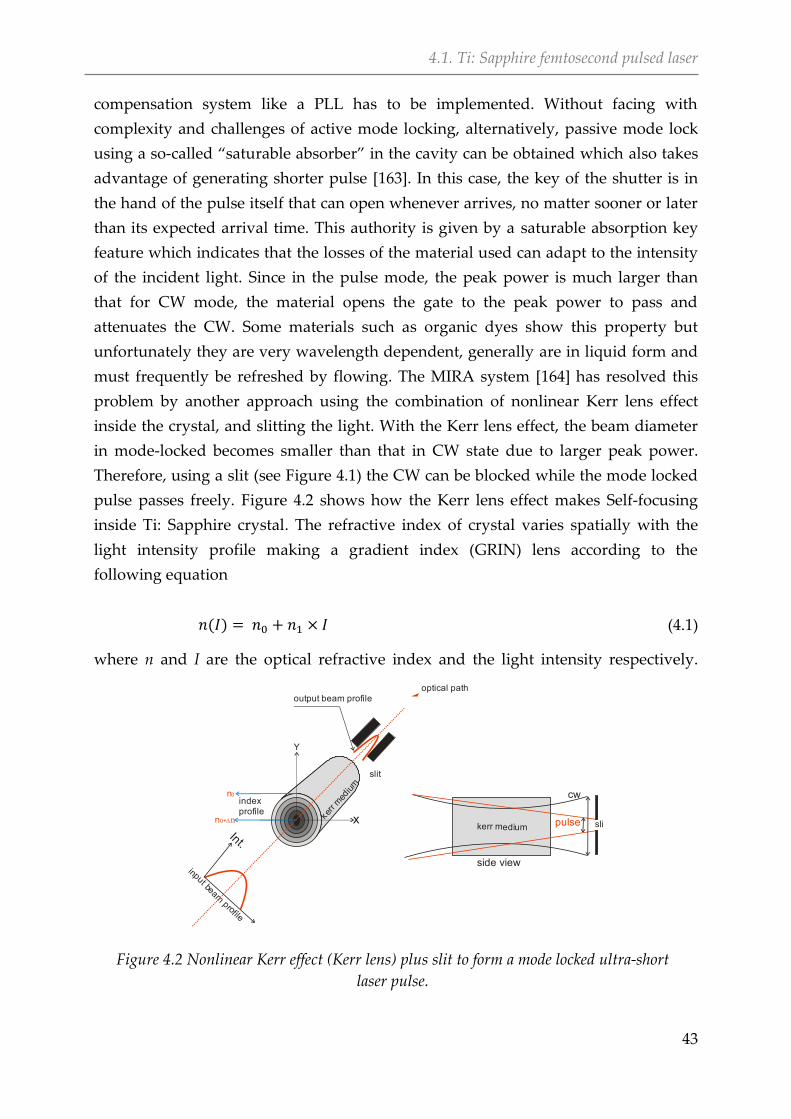
4.1. Ti: Sapphire femtosecond pulsed laser
43
compensation system like a PLL has to be implemented. Without facing with
complexity and challenges of active mode locking, alternatively, passive mode lock
using a so-called “saturable absorber” in the cavity can be obtained which also takes
advantage of generating shorter pulse [163]. In this case, the key of the shutter is in
the hand of the pulse itself that can open whenever arrives, no matter sooner or later
than its expected arrival time. This authority is given by a saturable absorption key
feature which indicates that the losses of the material used can adapt to the intensity
of the incident light. Since in the pulse mode, the peak power is much larger than
that for CW mode, the material opens the gate to the peak power to pass and
attenuates the CW. Some materials such as organic dyes show this property but
unfortunately they are very wavelength dependent, generally are in liquid form and
must frequently be refreshed by flowing. The MIRA system [164] has resolved this
problem by another approach using the combination of nonlinear Kerr lens effect
inside the crystal, and slitting the light. With the Kerr lens effect, the beam diameter
in mode-locked becomes smaller than that in CW state due to larger peak power.
Therefore, using a slit (see Figure 4.1) the CW can be blocked while the mode locked
pulse passes freely. Figure 4.2 shows how the Kerr lens effect makes Self-focusing
inside Ti: Sapphire crystal. The refractive index of crystal varies spatially with the
light intensity profile making a gradient index (GRIN) lens according to the
following equation
( ) (4.1)
where n and I are the optical refractive index and the light intensity respectively.
x
Y
n0+ nΔ
input beam profile
output beam profile
slit
kerr m
ediu
m
optical path
n0
index profile
kerr medium
cw
pulse slit
side view
Int.
Figure 4.2 Nonlinear Kerr effect (Kerr lens) plus slit to form a mode locked ultra-short
laser pulse.
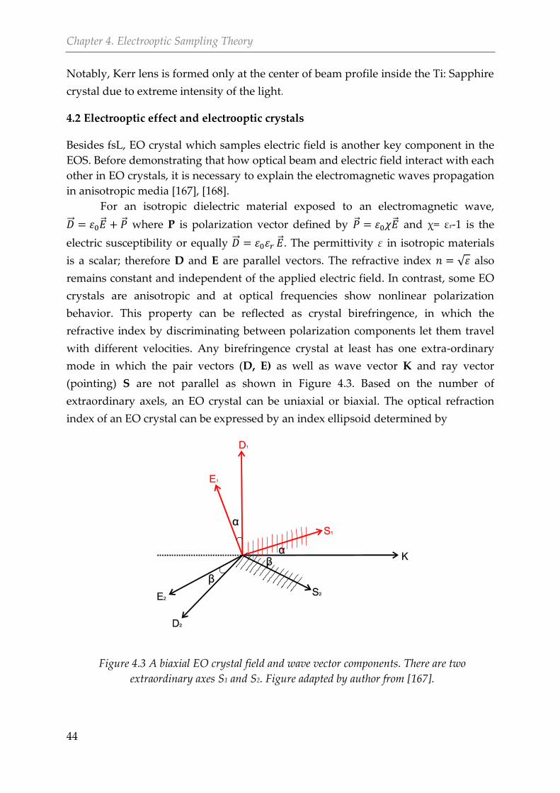
Chapter 4. Electrooptic Sampling Theory
44
Notably, Kerr lens is formed only at the center of beam profile inside the Ti: Sapphire
crystal due to extreme intensity of the light. [166]
4.2 Electrooptic effect and electrooptic crystals
Besides fsL, EO crystal which samples electric field is another key component in the
EOS. Before demonstrating that how optical beam and electric field interact with each
other in EO crystals, it is necessary to explain the electromagnetic waves propagation
in anisotropic media [167], [168].
For an isotropic dielectric material exposed to an electromagnetic wave,
where P is polarization vector defined by and χ= εr-1 is the
electric susceptibility or equally . The permittivity ε in isotropic materials
is a scalar; therefore D and E are parallel vectors. The refractive index √ also
remains constant and independent of the applied electric field. In contrast, some EO
crystals are anisotropic and at optical frequencies show nonlinear polarization
behavior. This property can be reflected as crystal birefringence, in which the
refractive index by discriminating between polarization components let them travel
with different velocities. Any birefringence crystal at least has one extra-ordinary
mode in which the pair vectors (D, E) as well as wave vector K and ray vector
(pointing) S are not parallel as shown in Figure 4.3. Based on the number of
extraordinary axels, an EO crystal can be uniaxial or biaxial. The optical refraction
index of an EO crystal can be expressed by an index ellipsoid determined by
Figure 4.3 A biaxial EO crystal field and wave vector components. There are two
extraordinary axes S1 and S2. Figure adapted by author from [167].
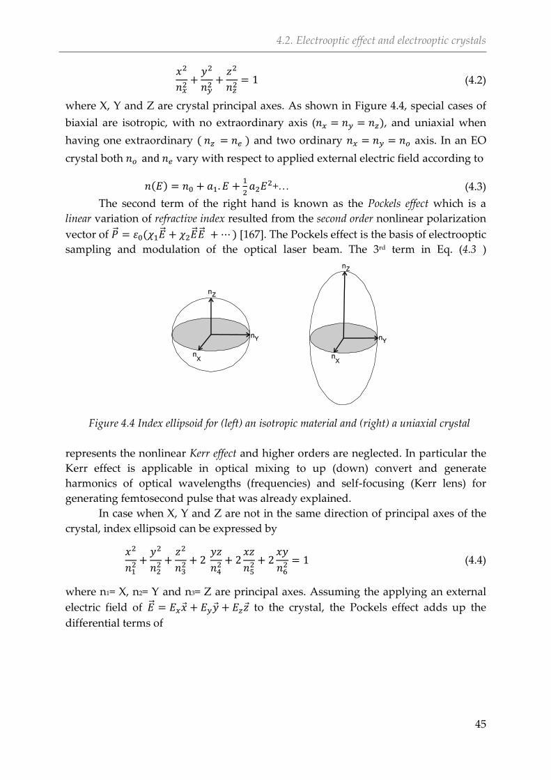
4.2. Electrooptic effect and electrooptic crystals
45
(4.2)
where X, Y and Z are crystal principal axes. As shown in Figure 4.4, special cases of
biaxial are isotropic, with no extraordinary axis ( ), and uniaxial when
having one extraordinary ( ) and two ordinary axis. In an EO
crystal both vary with respect to applied external electric field according to
( )
+… (4.3)
The second term of the right hand is known as the Pockels effect which is a
linear variation of refractive index resulted from the second order nonlinear polarization
vector of ( ) [167]. The Pockels effect is the basis of electrooptic
sampling and modulation of the optical laser beam. The 3rd term in Eq. (4.3 )
represents the nonlinear Kerr effect and higher orders are neglected. In particular the
Kerr effect is applicable in optical mixing to up (down) convert and generate
harmonics of optical wavelengths (frequencies) and self-focusing (Kerr lens) for
generating femtosecond pulse that was already explained.
In case when X, Y and Z are not in the same direction of principal axes of the
crystal, index ellipsoid can be expressed by
(4.4)
where n1= X, n2= Y and n3= Z are principal axes. Assuming the applying an external
electric field of to the crystal, the Pockels effect adds up the
differential terms of
Figure 4.4 Index ellipsoid for (left) an isotropic material and (right) a uniaxial crystal
Chapter 4. Electrooptic Sampling Theory
46
(
(
)
(
)
(
)
(
)
(
)
(
) )
=
(
)
(
) (4.5)
to the unbiased refractive index, where rij [pm/V] are EO coefficients of a 6×3 matrix
which is a simplified form of EO tensor due to zero symmetrical elements. To better
understanding the EO effect, it is better to illustrate an example for the case of LiTaO3
crystal. To this end, Figure 4.5 shows an X-cut LiTaO3 which is a 3m1 uniaxial crystal
and its differential refractive index is expressed by
(
(
)
(
)
(
)
(
)
(
)
(
)
)
=
(
)
(
) (4.6)
where are ordinary , is extraordinary axis and
initial values , while EO coefficients are
all in [pm/V] [169], [170]. By applying an external
electric field in the Z direction, therefore whereas , and finally the
index ellipsoid in Eq. (4.4) yields
(
)
(
)
(
)
(4.7)
The deviation of refractive indexes including ( ) ( )
is very small in comparison with their initial values and according to the
approximation of (
) (
) the new refractive indexes yields
(
) (
) (4.8)
In a real condition, if an optical beam with polarization in the XZ plane (see
Figure 4.5), expressed by ( ) travels through the crystal in the Y
direction, the phase of the X and Z field components changes according to
1 Crystal symmetry axis
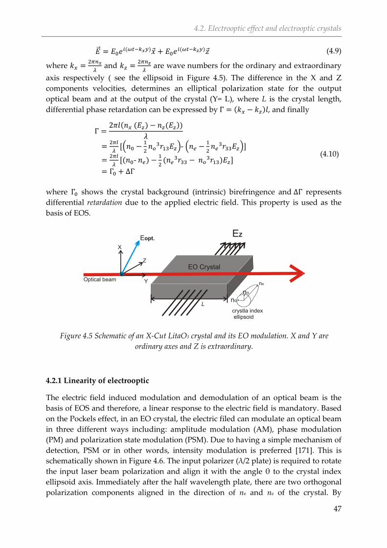
4.2. Electrooptic effect and electrooptic crystals
47
( )
( ) (4.9)
where
and
are wave numbers for the ordinary and extraordinary
axis respectively ( see the ellipsoid in Figure 4.5). The difference in the X and Z
components velocities, determines an elliptical polarization state for the output
optical beam and at the output of the crystal (Y= L), where L is the crystal length,
differential phase retardation can be expressed by ( ) , and finally
( ( ) ( ))
[(
)- (
)]
[( - )
(
) ]
(4.10)
where shows the crystal background (intrinsic) birefringence and represents
differential retardation due to the applied electric field. This property is used as the
basis of EOS.
Linearity of electrooptic 4.2.1
The electric field induced modulation and demodulation of an optical beam is the
basis of EOS and therefore, a linear response to the electric field is mandatory. Based
on the Pockels effect, in an EO crystal, the electric filed can modulate an optical beam
in three different ways including: amplitude modulation (AM), phase modulation
(PM) and polarization state modulation (PSM). Due to having a simple mechanism of
detection, PSM or in other words, intensity modulation is preferred [171]. This is
schematically shown in Figure 4.6. The input polarizer (λ/2 plate) is required to rotate
the input laser beam polarization and align it with the angle θ to the crystal index
ellipsoid axis. Immediately after the half wavelength plate, there are two orthogonal
polarization components aligned in the direction of ne and ne of the crystal. By
Z
Y
X
EZ
Optical beam
EO Crystal
crystla index ellipsoid
Eopt.
L
ne
no
no
Figure 4.5 Schematic of an X-Cut LitaO3 crystal and its EO modulation. X and Y are
ordinary axes and Z is extraordinary.
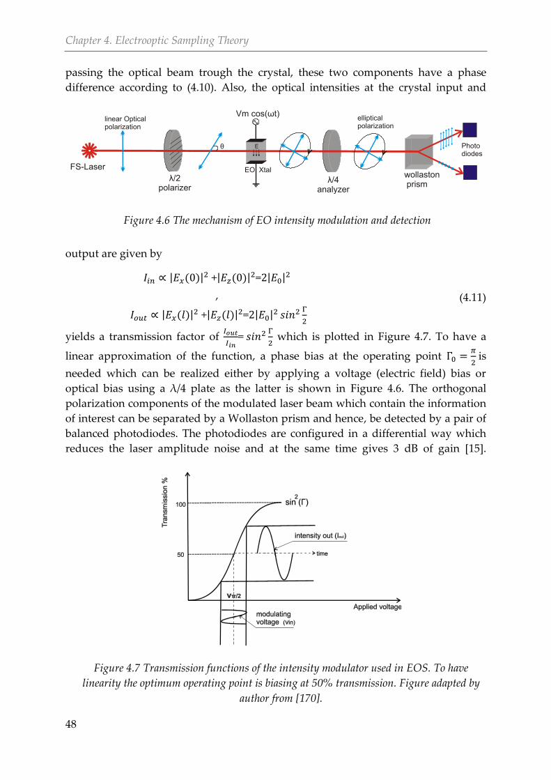
Chapter 4. Electrooptic Sampling Theory
48
passing the optical beam trough the crystal, these two components have a phase
difference according to (4.10). Also, the optical intensities at the crystal input and
output are given by
| ( )| +| ( )| = | |
,
| ( )| +| ( )|
= | |
(4.11)
yields a transmission factor of
=
which is plotted in Figure 4.7. To have a
linear approximation of the function, a phase bias at the operating point
is
needed which can be realized either by applying a voltage (electric field) bias or
optical bias using a λ/4 plate as the latter is shown in Figure 4.6. The orthogonal
polarization components of the modulated laser beam which contain the information
of interest can be separated by a Wollaston prism and hence, be detected by a pair of
balanced photodiodes. The photodiodes are configured in a differential way which
reduces the laser amplitude noise and at the same time gives 3 dB of gain [15].
E
FS-Laser
linear Optical polarization
λ/2polarizer
λ/4analyzer
θ
wollaston prism
elliptical polarization
Photo diodes
Figure 4.6 The mechanism of EO intensity modulation and detection
Figure 4.7 Transmission functions of the intensity modulator used in EOS. To have
linearity the optimum operating point is biasing at 50% transmission. Figure adapted by
author from [170].
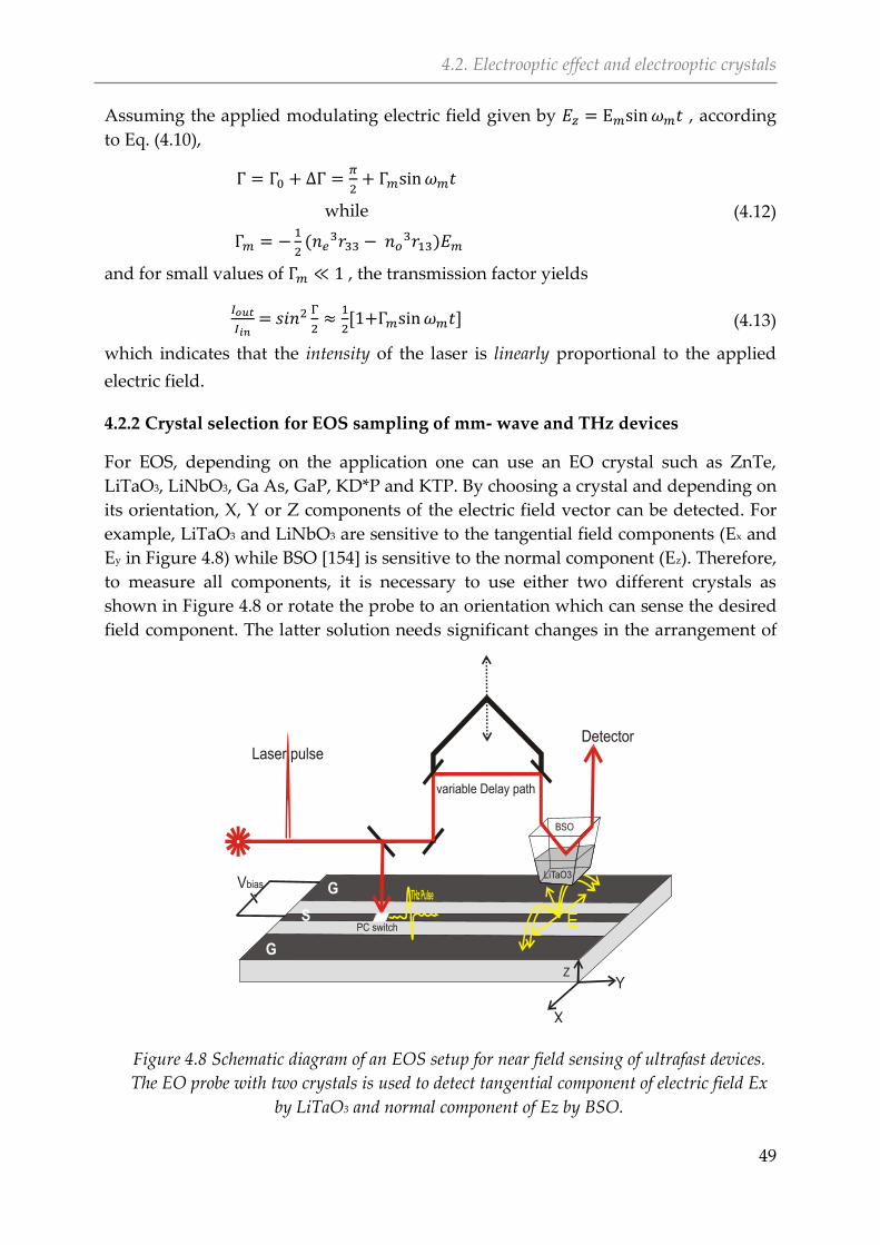
4.2. Electrooptic effect and electrooptic crystals
49
Assuming the applied modulating electric field given by , according
to Eq. (4.10),
while
(
)
(4.12)
and for small values of , the transmission factor yields
=
[1+ ] (4.13)
which indicates that the intensity of the laser is linearly proportional to the applied
electric field.
Crystal selection for EOS sampling of mm- wave and THz devices 4.2.2
For EOS, depending on the application one can use an EO crystal such as ZnTe,
LiTaO3, LiNbO3, Ga As, GaP, KD*P and KTP. By choosing a crystal and depending on
its orientation, X, Y or Z components of the electric field vector can be detected. For
example, LiTaO3 and LiNbO3 are sensitive to the tangential field components (Ex and
Ey in Figure 4.8) while BSO [154] is sensitive to the normal component (Ez). Therefore,
to measure all components, it is necessary to use either two different crystals as
shown in Figure 4.8 or rotate the probe to an orientation which can sense the desired
field component. The latter solution needs significant changes in the arrangement of
Laser pulse
variable Delay path
G
G
S
X
YZ
Detector
PC switch
Vbias
E
BSO
LiTaO3
Figure 4.8 Schematic diagram of an EOS setup for near field sensing of ultrafast devices.
The EO probe with two crystals is used to detect tangential component of electric field Ex
by LiTaO3 and normal component of Ez by BSO.
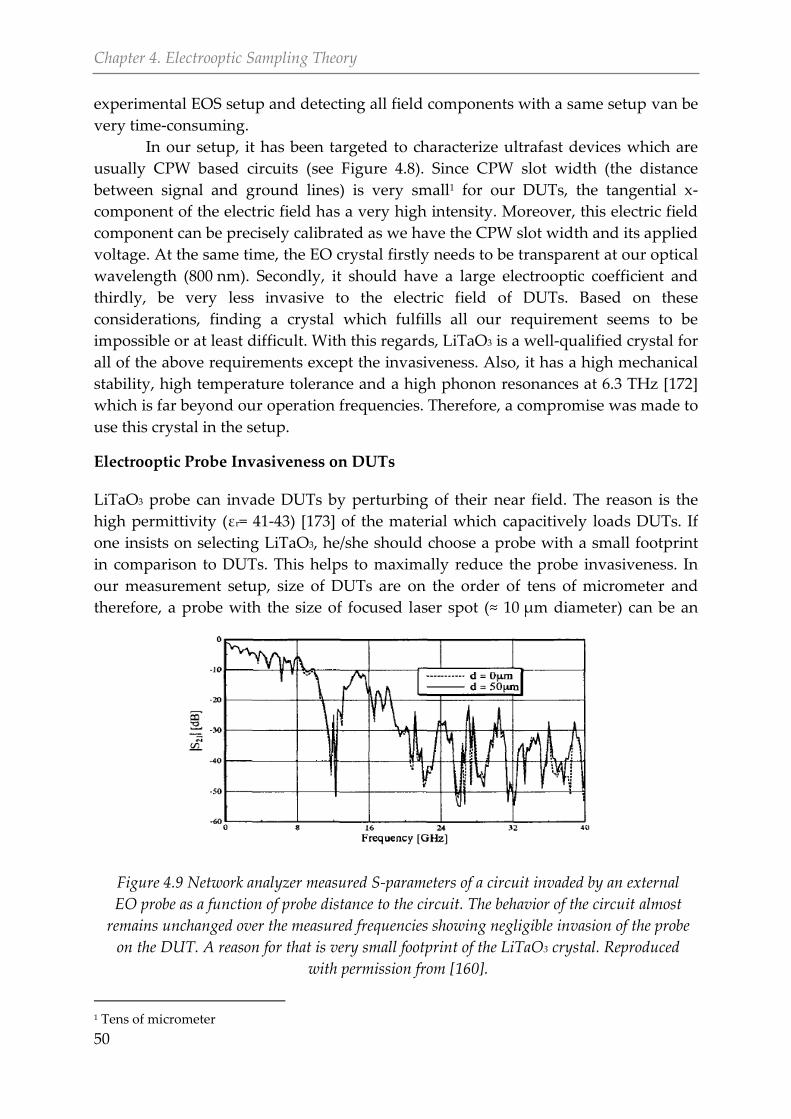
Chapter 4. Electrooptic Sampling Theory
50
experimental EOS setup and detecting all field components with a same setup van be
very time-consuming.
In our setup, it has been targeted to characterize ultrafast devices which are
usually CPW based circuits (see Figure 4.8). Since CPW slot width (the distance
between signal and ground lines) is very small1 for our DUTs, the tangential x-
component of the electric field has a very high intensity. Moreover, this electric field
component can be precisely calibrated as we have the CPW slot width and its applied
voltage. At the same time, the EO crystal firstly needs to be transparent at our optical
wavelength (800 nm). Secondly, it should have a large electrooptic coefficient and
thirdly, be very less invasive to the electric field of DUTs. Based on these
considerations, finding a crystal which fulfills all our requirement seems to be
impossible or at least difficult. With this regards, LiTaO3 is a well-qualified crystal for
all of the above requirements except the invasiveness. Also, it has a high mechanical
stability, high temperature tolerance and a high phonon resonances at 6.3 THz [172]
which is far beyond our operation frequencies. Therefore, a compromise was made to
use this crystal in the setup.
Electrooptic Probe Invasiveness on DUTs
LiTaO3 probe can invade DUTs by perturbing of their near field. The reason is the
high permittivity (εr= 41-43) [173] of the material which capacitively loads DUTs. If
one insists on selecting LiTaO3, he/she should choose a probe with a small footprint
in comparison to DUTs. This helps to maximally reduce the probe invasiveness. In
our measurement setup, size of DUTs are on the order of tens of micrometer and
therefore, a probe with the size of focused laser spot (≈ 10 μm diameter) can be an
1 Tens of micrometer
Figure 4.9 Network analyzer measured S-parameters of a circuit invaded by an external
EO probe as a function of probe distance to the circuit. The behavior of the circuit almost
remains unchanged over the measured frequencies showing negligible invasion of the probe
on the DUT. A reason for that is very small footprint of the LiTaO3 crystal. Reproduced
with permission from [160].
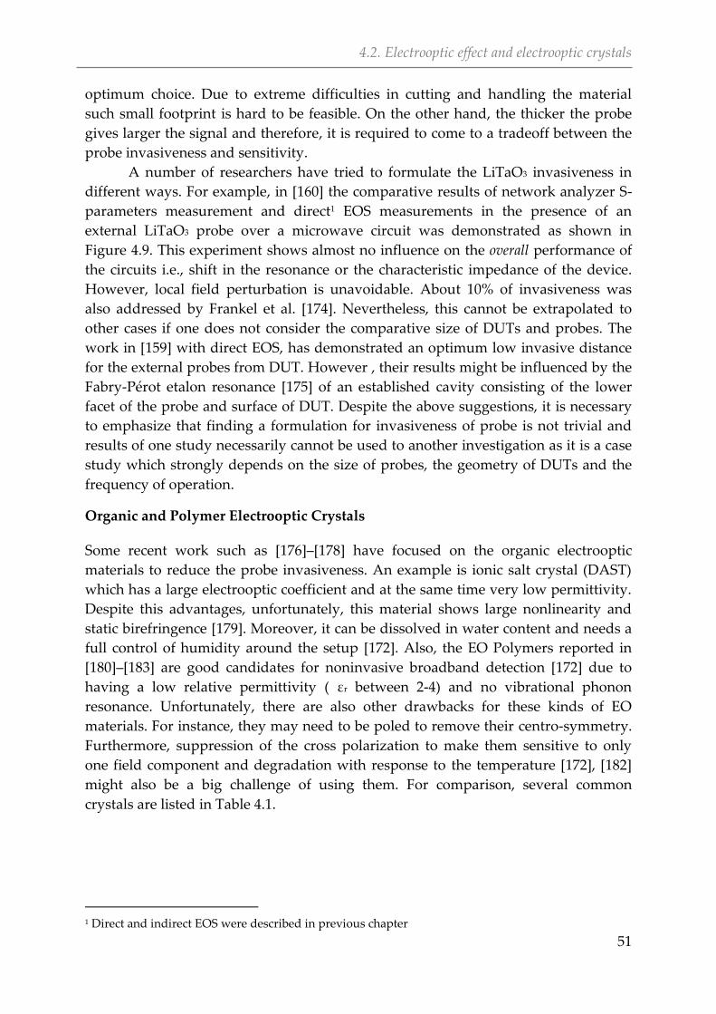
4.2. Electrooptic effect and electrooptic crystals
51
optimum choice. Due to extreme difficulties in cutting and handling the material
such small footprint is hard to be feasible. On the other hand, the thicker the probe
gives larger the signal and therefore, it is required to come to a tradeoff between the
probe invasiveness and sensitivity.
A number of researchers have tried to formulate the LiTaO3 invasiveness in
different ways. For example, in [160] the comparative results of network analyzer S-
parameters measurement and direct1 EOS measurements in the presence of an
external LiTaO3 probe over a microwave circuit was demonstrated as shown in
Figure 4.9. This experiment shows almost no influence on the overall performance of
the circuits i.e., shift in the resonance or the characteristic impedance of the device.
However, local field perturbation is unavoidable. About 10% of invasiveness was
also addressed by Frankel et al. [174]. Nevertheless, this cannot be extrapolated to
other cases if one does not consider the comparative size of DUTs and probes. The
work in [159] with direct EOS, has demonstrated an optimum low invasive distance
for the external probes from DUT. However , their results might be influenced by the
Fabry-Pérot etalon resonance [175] of an established cavity consisting of the lower
facet of the probe and surface of DUT. Despite the above suggestions, it is necessary
to emphasize that finding a formulation for invasiveness of probe is not trivial and
results of one study necessarily cannot be used to another investigation as it is a case
study which strongly depends on the size of probes, the geometry of DUTs and the
frequency of operation.
Organic and Polymer Electrooptic Crystals
Some recent work such as [176]–[178] have focused on the organic electrooptic
materials to reduce the probe invasiveness. An example is ionic salt crystal (DAST)
which has a large electrooptic coefficient and at the same time very low permittivity.
Despite this advantages, unfortunately, this material shows large nonlinearity and
static birefringence [179]. Moreover, it can be dissolved in water content and needs a
full control of humidity around the setup [172]. Also, the EO Polymers reported in
[180]–[183] are good candidates for noninvasive broadband detection [172] due to
having a low relative permittivity ( εr between 2-4) and no vibrational phonon
resonance. Unfortunately, there are also other drawbacks for these kinds of EO
materials. For instance, they may need to be poled to remove their centro-symmetry.
Furthermore, suppression of the cross polarization to make them sensitive to only
one field component and degradation with response to the temperature [172], [182]
might also be a big challenge of using them. For comparison, several common
crystals are listed in Table 4.1.
1 Direct and indirect EOS were described in previous chapter
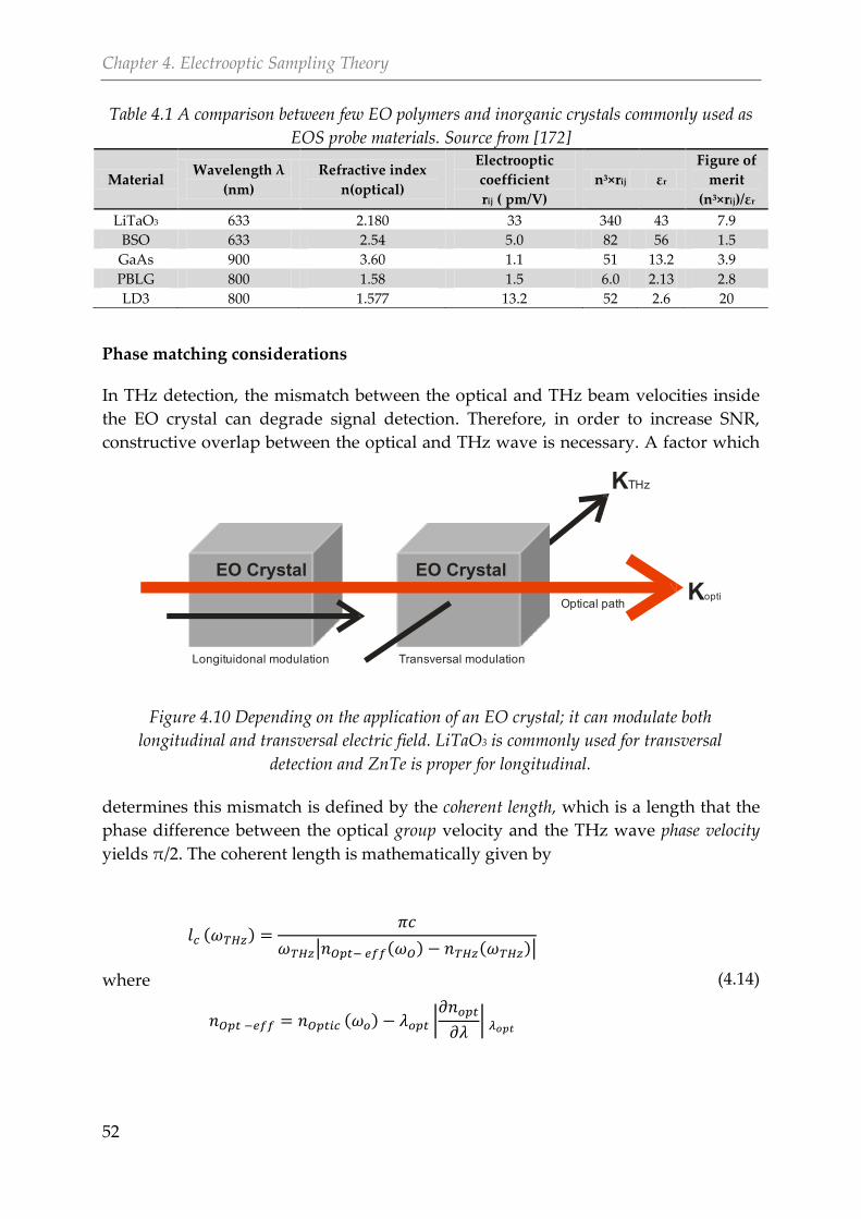
Chapter 4. Electrooptic Sampling Theory
52
Phase matching considerations
In THz detection, the mismatch between the optical and THz beam velocities inside
the EO crystal can degrade signal detection. Therefore, in order to increase SNR,
constructive overlap between the optical and THz wave is necessary. A factor which
determines this mismatch is defined by the coherent length, which is a length that the
phase difference between the optical group velocity and the THz wave phase velocity
yields π/2. The coherent length is mathematically given by
( )
| ( ) ( )|
where
( ) |
|
(4.14)
Table 4.1 A comparison between few EO polymers and inorganic crystals commonly used as
EOS probe materials. Source from [172]
Material Wavelength λ
(nm)
Refractive index
n(optical)
Electrooptic
coefficient
rij ( pm/V)
n3×rij εr
Figure of
merit
(n3×rij)/εr
LiTaO3 633 2.180 33 340 43 7.9
BSO 633 2.54 5.0 82 56 1.5
GaAs 900 3.60 1.1 51 13.2 3.9
PBLG 800 1.58 1.5 6.0 2.13 2.8
LD3 800 1.577 13.2 52 2.6 20
EO Crystal
Longituidonal modulation Transversal modulation
Optical path
EO Crystal
Koptic
KTHz
Figure 4.10 Depending on the application of an EO crystal; it can modulate both
longitudinal and transversal electric field. LiTaO3 is commonly used for transversal
detection and ZnTe is proper for longitudinal.
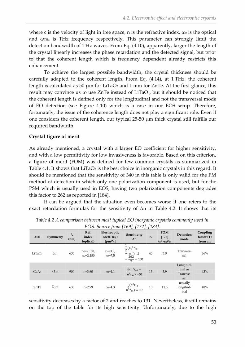
4.2. Electrooptic effect and electrooptic crystals
53
where c is the velocity of light in free space, n is the refractive index, ω0 is the optical
and ωTHz is THz frequency respectively. This parameter can strongly limit the
detection bandwidth of THz waves. From Eq. (4.10), apparently, larger the length of
the crystal linearly increases the phase retardation and the detected signal, but prior
to that the coherent length which is frequency dependent already restricts this
enhancement.
To achieve the largest possible bandwidth, the crystal thickness should be
carefully adapted to the coherent length. From Eq. (4.14), at 1 THz, the coherent
length is calculated as 50 μm for LiTaO3 and 1 mm for ZnTe. At the first glance, this
result may convince us to use ZnTe instead of LiTaO3, but it should be noticed that
the coherent length is defined only for the longitudinal and not the transversal mode
of EO detection (see Figure 4.10) which is a case in our EOS setup. Therefore,
fortunately, the issue of the coherence length does not play a significant role. Even if
one considers the coherent length, our typical 25-50 μm thick crystal still fulfills our
required bandwidth.
Crystal figure of merit
As already mentioned, a crystal with a larger EO coefficient for higher sensitivity,
and with a low permittivity for low invasiveness is favorable. Based on this criterion,
a figure of merit (FOM) was defined for few common crystals as summarized in
Table 4.1. It shows that LiTaO3 is the best choice in inorganic crystals in this regard. It
should be mentioned that the sensitivity of 340 in this table is only valid for the PM
method of detection in which only one polarization component is used, but for the
PSM which is usually used in EOS, having two polarization components degrades
this factor to 262 as reported in [184].
It can be argued that the situation even becomes worse if one refers to the
exact retardation formulas for the sensitivity of Δn in Table 4.2. It shows that its
sensitivity decreases by a factor of 2 and reaches to 131. Nevertheless, it still remains
on the top of the table for its high sensitivity. Unfortunately, due to the high
Table 4.2 A comparison between most typical EO inorganic crystals commonly used in
EOS. Source from [169], [172], [184].
Xtal Symmetry λ
(nm)
Ref.
index
(optical)
Electrooptic
coeff. (rij )
[pm/V]
Sensitivity
Δn εr
FOM
[172]
(n3×rij)/εr
Detection
mode
Coupling
factor (T)
from air
LiTaO3 3m 633 ne=2.180,
no=2.180
r33=33 ,
r13=7.5
(
)
43 3.0 Transver-
sal 26%
GaAs 3m 900 n=3.60 r41=1.1
(
) 51 13 3.9
Longitud-
inal or
Transve-
sal
43%
ZnTe 3m 633 n=2.99 r41=4.3
(
) 115 10 11.5
usually
longitud-
inal
48%
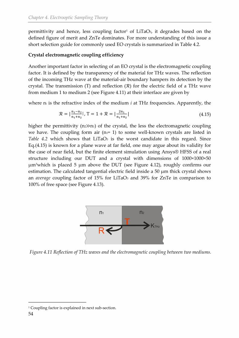
Chapter 4. Electrooptic Sampling Theory
54
TR
n1 n2
KTHz
Figure 4.11 Reflection of THz waves and the electromagnetic coupling between two mediums.
permittivity and hence, less coupling factor1 of LiTaO3, it degrades based on the
defined figure of merit and ZnTe dominates. For more understanding of this issue a
short selection guide for commonly used EO crystals is summarized in Table 4.2.
Crystal electromagnetic coupling efficiency
Another important factor in selecting of an EO crystal is the electromagnetic coupling
factor. It is defined by the transparency of the material for THz waves. The reflection
of the incoming THz wave at the material-air boundary hampers its detection by the
crystal. The transmission (T) and reflection ( ) for the electric field of a THz wave
from medium 1 to medium 2 (see Figure 4.11) at their interface are given by
where ni is the refractive index of the medium i at THz frequencies. Apparently, the
higher the permittivity (n2≫n1) of the crystal, the less the electromagnetic coupling
we have. The coupling form air (n1= 1) to some well-known crystals are listed in
Table 4.2 which shows that LiTaO3 is the worst candidate in this regard. Since
Eq.(4.15) is known for a plane wave at far field, one may argue about its validity for
the case of near field, but the finite element simulation using Ansys® HFSS of a real
structure including our DUT and a crystal with dimensions of 1000×1000×50
μm3which is placed 5 μm above the DUT (see Figure 4.12), roughly confirms our
estimation. The calculated tangential electric field inside a 50 μm thick crystal shows
an average coupling factor of 15% for LiTaO3 and 39% for ZnTe in comparison to
100% of free space (see Figure 4.13).
1 Coupling factor is explained in next sub-section.
|
|, |
| (4.15)
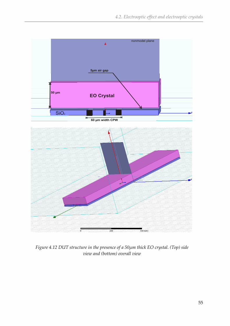
4.2. Electrooptic effect and electrooptic crystals
55
EO Crystal
5 air gap µm
60 µm width CPW
50 µm
SiO2
nonmodel plane
Figure 4.12 DUT structure in the presence of a 50µm thick EO crystal. (Top) side
view and (bottom) overall view
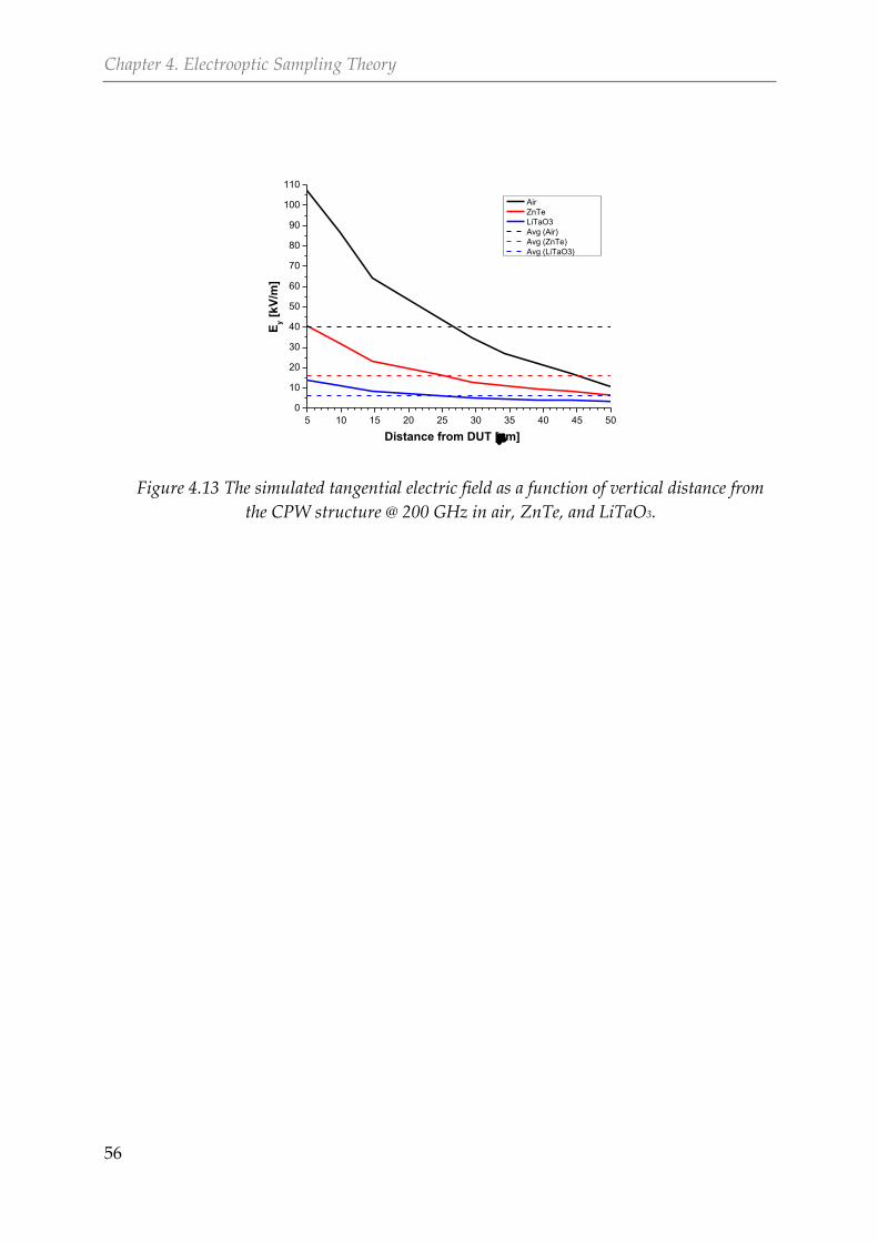
Chapter 4. Electrooptic Sampling Theory
56
5 10 15 20 25 30 35 40 45 50
0
10
20
30
40
50
60
70
80
90
100
110
Ey [
kV
/m]
Distance from DUT [m]
Air
ZnTe
LiTaO3
Avg (Air)
Avg (ZnTe)
Avg (LiTaO3)
Figure 4.13 The simulated tangential electric field as a function of vertical distance from
the CPW structure @ 200 GHz in air, ZnTe, and LiTaO3.
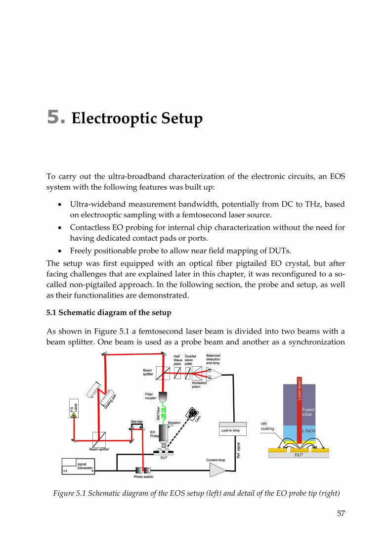
57
Electrooptic Setup 5.
To carry out the ultra-broadband characterization of the electronic circuits, an EOS
system with the following features was built up:
Ultra-wideband measurement bandwidth, potentially from DC to THz, based
on electrooptic sampling with a femtosecond laser source.
Contactless EO probing for internal chip characterization without the need for
having dedicated contact pads or ports.
Freely positionable probe to allow near field mapping of DUTs.
The setup was first equipped with an optical fiber pigtailed EO crystal, but after
facing challenges that are explained later in this chapter, it was reconfigured to a so-
called non-pigtailed approach. In the following section, the probe and setup, as well
as their functionalities are demonstrated.
5.1 Schematic diagram of the setup
As shown in Figure 5.1 a femtosecond laser beam is divided into two beams with a
beam splitter. One beam is used as a probe beam and another as a synchronization
Figure 5.1 Schematic diagram of the EOS setup (left) and detail of the EO probe tip (right)
Chapter 5. Electrooptic Setup
58
beam for heterodyne detection. Obviously, synchronization of a heterodyne system is
very critical, therefore, in EOS, the laser as sampler should be synchronized with the
sampled signal of DUTs. Since the laser is an optical system and DUT is driven by a
microwave generator, hence, a component for conversion of the optical to an electric
signal is required. This can be achieved using a PC Auston switch which is
specifically designed to operate at microwave frequencies. The PC switch plays the
role of a harmonic mixer that mixes the microwave frequency with the higher
harmonics of the laser repetition rate. Assuming the laser repetition frequency of fl
(typically 75 MHz) and fm as the microwave frequency, the output frequency of photo
switch mixer is , where n is the laser harmonic number (see
Figure 5.1). This offset frequency ∆f can easily be adjusted in the range of kHz or
MHz and used as external trigger signal for the lock-in amplifier. This offset
frequency can be stabilized at a reference frequency fr (usually between 10 kHz to 100
kHz) (not shown in Figure 5.1)1 from an external signal generator using a PLL
system. While the laser is synchronized to the microwave generator, the probe beam
samples the signal of DUT with an electrooptic crystal based on the Pockels effect
which was explained in the previous chapter. The reflected laser beam from a highly
reflective (HR) coating at the bottom facet of the LiTaO3 crystal (see Figure 5.1 -right)
which is modulated by the electric field of DUT is then separated from the incident
beam by another beam splitter. This beam hence, by passing through a λ/4 plate and
a Wollaston prism is prepared for the intensity detection with the aid of electronics
including a pair of balanced photodiodes, a low noise current amplifier and either a
lock-in amplifier or a data acquisition. The delay stage provides a time delay between
the sampling laser beam and the sampled signal. The grating pair in the setup is used
for dispersion compensation of the fiber-based EO probe which is explained later in
this chapter. To understand the system characteristics in the following sections, key
components of the setup are described in detail.
The pigtailed electrooptic probe 5.1.1
The most crucial component of the system is the EO probe, consisting of a fiber
coupled LiTaO3 crystal [150], [152] which samples the electric field from DUTs. The
amplitude and phase of the DUT electric field can thereby be detected from the
modulation of the optical polarization state of the reflected laser beam. As mentioned
in the previous chapter, LiTaO3 is advantageous over other crystals and its
application has frequently been addressed [113], [115], [133]. Nevertheless, it is not
the best choice due to its high invasiveness2. The crystal has a 50 μm (25 μm)
thickness and is placed on a 0.9 mm×0.9 mm fused silica support. This combination,
hence, is glued to a GRIN lens which is pigtailed with a 780-HP Nufern [185] fiber.
This allows an efficient optical coupling and focus of the probe laser beam at a
diameter less than 10 µm at the probe tip. The pigtailed optical fiber, shown in
1 See MM-LS in Chapter 7 for detail. 2 See Chapter 4.
5.1. Schematic diagram of the setup
59
Figure 5.2, provides flexible maneuver and positioning of the probe in the setup.
Since passing the femtosecond laser pulse trough this fiber faces dispersion, a
dispersion compensation unit consisting of a grating pair is integrated with the setup.
This combination provides a laser pulse width < 200 fs at the probe tip where the
THz signal is detected and theoretically ensures a detection bandwidth up to 5 THz
(~ 1/ 200 fs). For comparison, without this compensation, a 2.5 m length fiber would
deliver broader than 5 ps laser pulses, which theoretically limits the system
bandwidth to frequencies below 200 GHz.
The photoconductive switch 5.1.2
A typical Auston [95] PC switch is made of a semiconductor substrate (or a
photoconductive thin film on a substrate), on which metallic electrodes are deposited
in a form of a 50 Ω microstrip line. By Illumination of laser beam on the gap between
two electrodes of microstrip transmission line, the semiconductor absorbs photons
and generates an enormous number of electron and hole pairs. The number of
generated carriers, evidently, depends on the semiconductor material quantum
efficiency and the laser beam power. As long as these charge carriers are alive, the
switch is turning on and conducting (low resistance state), otherwise it remains in
off-state (high resistance). Using this mechanism, the harmonics of the laser
Figure 5.2 The fiber pigtailed EO probe with 50 μm thick crystal and the detail of the tip.
Figure 5.3 Harmonic mixing of a microwave signal and laser pulse.
Chapter 5. Electrooptic Setup
60
repetition rate can mix with a microwave signal which is fed to the switch as shown
in Figure 5.3. As the switch has to efficiently work at the microwave (6-20 GHz)
frequencies, high frequency considerations must be taken into account. For this
reason, the switch operation in off and on states needs to be characterized.
The current density of the switch in both on and off cases can be described by
(5.1)
where,
(5.2)
are conduction and displacement current densities respectively. Also, for n and p
carriers the conductivity is
(5.3)
where µ is the mobility and q is the electron charge quanta. In off-state, jd is
dominated because of the capacitive coupling and by illuminating the switch (on-
state), the conduction current rapidly increases due to existing of the carriers, and
this state lasts until carriers recombine. A detailed balance of photoconductive switch
dimensions and the carrier lifetime (i.e. material choice) is needed to deliver a high
efficiency and a good on/off ratio. In our design, intrinsic GaAs with a carrier lifetime
of the order of 10-9 to 10-8 s was used. This is sufficiently short, in comparison to the
+-+
-++
-+-+
+-+
-+la
se
r be
am
GaAs
RT/Duroid 6010
0.1mm air gap
silver paint2-port
3-port
Δf
Δf
50Ω
(a) (b)
Figure 5.4 The photoconductive switch using intrinsic GaAs (εr=10.9) substrate and
deposited by a gold layer with thickness of 250nm 50 Ω transmission line. (a) Two port and
three port configuration, (b) the cross section of the switch which is embedded in RT/Duroid
6010 (εr=10.2, h=1.29mm) substrate.
5.1. Schematic diagram of the setup
61
laser repetition period1 81.3 10 and long compared with the microwave signal
period 1010671 . (f= 6 GHz). At first sight, it seems that, with this characteristic, the
switch is not fast enough, however, in reality, the carrier lifetime is shorter than that
for the theoretical values due to metal to semiconductor transitions and surface
recombination.
The dimensions of the photoconductive switch are chosen to maximize the
photoconductive switch efficiency. Assuming driving the photoconductive switch
with 0 dBm microwave signal power, for a gap length of g= 50 µm, an average
electron transit time of the order of 91092 ..E
gnt
is estimated [170].
In theory, the response of switch to the femtosecond pulse is exponential with
decay equal to the total carrier lifetime (i.e., the average for the material). The switch
mixes the femtosecond pulse with microwave signal (VRF) and hence, the output
signal yields ( ), where g(t) is the time gating function in response to
the femtosecond laser pulse. A worst case scenario can be calculated using a
recombination carrier lifetime of 810n s close to the period of the laser TL= 810331 . s,
but two order of magnitude longer than the microwave signal period. Even with this
long decay time, the short rise time g(t) enables sampling of the microwave signal
resulting in a kHz range beat frequency (see Figure 5.3). Evidently, for sampling
higher frequencies, e.g. at mm-wave, it is therefore, crucial to design an appropriate
switch with a high presence of surface and doping induced bulk recombination sites
to reduce the effective carrier lifetime [186]. As discussed in Chapter 3, Lt-GaAs
carrier lifetimes is down to few hundreds of fs [98]. However, this drastically can
decrease the photoconductive switch efficiency due to much smaller mobility.
1 Repetition frequency of the laser f= 76 MHz
Figure 5.5 (a) Fabricated photoconductive switch mounted on substrate plus a test 50 Ω
transmission line, (b) a micrograph of a 10 μm-gap of the switch. The gap is simple and not
interdigitated.
Chapter 5. Electrooptic Setup
62
Our photoconductive switch was realized by deposition of a gold microstrip
lines with 50 Ω characteristics impedance on a 6×6 mm2 GaAs piece of wafer and
hence with silver paint connected to 50 Ω line on a 5 cm ×5 cm RT/Duroid 6010 (εr=
10.2, h= 1.27mm) substrate. This combination allows mounting the switch on
standard optical mounts in the setup. Figure 5.4 shows the design strategies and
cross section of the embedded photoconductive switch. A thin layer (0.1 mm) of air
between GaAs and RT/Duroid 6010, as surface roughness, has been taken into
account for impedance calculations of the microstrip line. Several configurations of
switches with different gap lengths were fabricated, and only one sample is shown in
Figure 5.5.
From the circuit model, in off-state, the switch acts as a series capacitance (for
the gap) and two shunt capacitance from the metal edges to the back ground plane
side of the microstrip line. The gap size plays a significantly important role in
particular in off-state. The larger the gap, the less the coupling capacitance and hence,
the larger isolation of the switch in off-state we have. In on-state, the switch acts like
a conductor and the gap size, as well as the laser beam power intensity govern the
amount of absorbed photons. The coupling in both states for different switches is
given in Table 5.1. From these results, it can be seen that a 3-port 20 µm gap switch
has the highest isolation in off-state, but in on-state also it might have a low value of
the coupling because of a mismatch caused by the loading of a stub on the 3rd port of
the switch. The next highest insertion loss (4 dB) in off-state is given for 50 µm gap,
realized with a two-port switch.
A successful operation of PC switches could be demonstrated after several
photoconductive switch optimization cycles. The quality and stability of the output
Table 5.1 Experimental results of different photo switches
Photo switch
High frequency
test insertion
loss (dB) (off-
state)
High
frequency test
(on-state)
Low frequency test
10 kHz, 1 V p-p
(off-state)
Low frequency
test 10 kHz,
1Vp-p(on-state)
50 Ω
transmission line
( RT/Duroid 6010
substrate)
0.5 NA NA NA
5µm gap switch -
2 port 1,6
Harmonic
unachievable
or difficult to
achieve
Current amplifier
output less than 2 mV
Current amplifier
output 8 Vp-p,
(distorted
waveform)
20 µm gap switch
-2 port 2,4 NA NA NA
20 µm gap 3-port 9,5 NA NA NA
50 µm gap
switch- 2-port 4,0
Clear
difference
signal
Current amplifier
output less than 2 mV
Current amplifier
output 20 Vp-p,
saturated
Note: Gain of current amplifier is 105 V/I
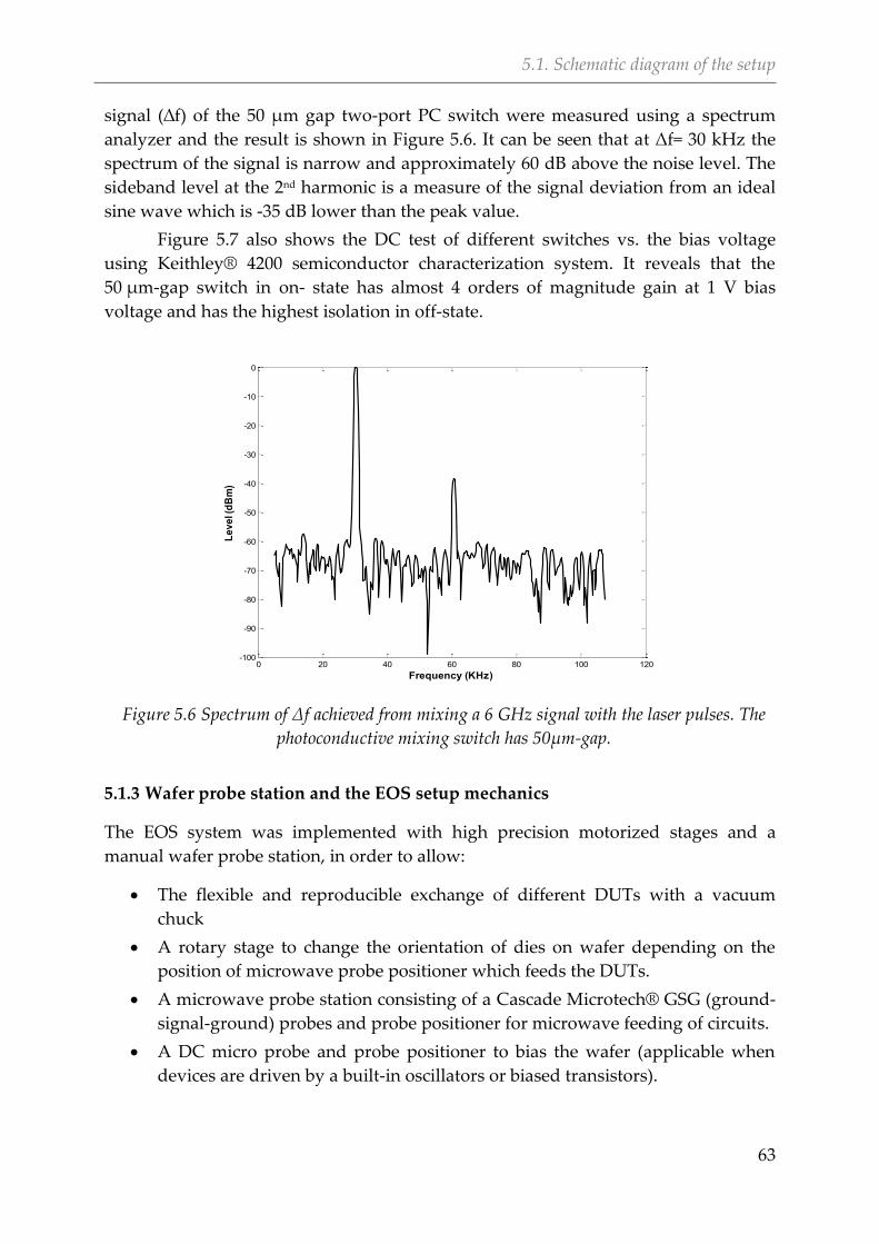
5.1. Schematic diagram of the setup
63
signal (∆f) of the 50 μm gap two-port PC switch were measured using a spectrum
analyzer and the result is shown in Figure 5.6. It can be seen that at Δf= 30 kHz the
spectrum of the signal is narrow and approximately 60 dB above the noise level. The
sideband level at the 2nd harmonic is a measure of the signal deviation from an ideal
sine wave which is -35 dB lower than the peak value.
Figure 5.7 also shows the DC test of different switches vs. the bias voltage
using Keithley® 4200 semiconductor characterization system. It reveals that the
50 μm-gap switch in on- state has almost 4 orders of magnitude gain at 1 V bias
voltage and has the highest isolation in off-state.
Wafer probe station and the EOS setup mechanics 5.1.3
The EOS system was implemented with high precision motorized stages and a
manual wafer probe station, in order to allow:
The flexible and reproducible exchange of different DUTs with a vacuum
chuck
A rotary stage to change the orientation of dies on wafer depending on the
position of microwave probe positioner which feeds the DUTs.
A microwave probe station consisting of a Cascade Microtech® GSG (ground-
signal-ground) probes and probe positioner for microwave feeding of circuits.
A DC micro probe and probe positioner to bias the wafer (applicable when
devices are driven by a built-in oscillators or biased transistors).
0 20 40 60 80 100 120-100
-90
-80
-70
-60
-50
-40
-30
-20
-10
0
Frequency (KHz)
Le
ve
l (d
Bm
)
Figure 5.6 Spectrum of Δf achieved from mixing a 6 GHz signal with the laser pulses. The
photoconductive mixing switch has 50μm-gap.
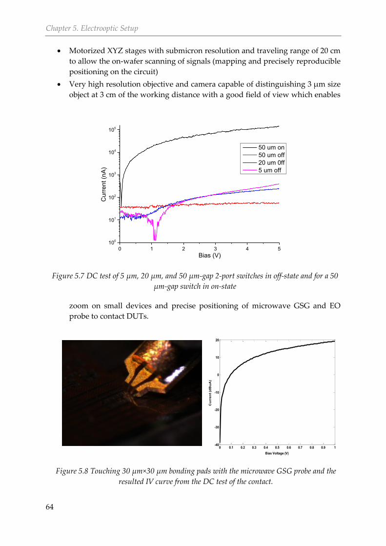
Chapter 5. Electrooptic Setup
64
Motorized XYZ stages with submicron resolution and traveling range of 20 cm
to allow the on-wafer scanning of signals (mapping and precisely reproducible
positioning on the circuit)
Very high resolution objective and camera capable of distinguishing 3 μm size
object at 3 cm of the working distance with a good field of view which enables
zoom on small devices and precise positioning of microwave GSG and EO
probe to contact DUTs.
0 0.1 0.2 0.3 0.4 0.5 0.6 0.7 0.8 0.9 1-40
-30
-20
-10
0
10
20
Bias Voltage (V)
Cu
rre
nt
(dB
uA
)
Figure 5.8 Touching 30 μm×30 μm bonding pads with the microwave GSG probe and the
resulted IV curve from the DC test of the contact.
0 1 2 3 4 5
100
101
102
103
104
105
Cu
rre
nt (n
A)
Bias (V)
50 um on
50 um off
20 um 0ff
5 um off
Figure 5.7 DC test of 5 µm, 20 µm, and 50 µm-gap 2-port switches in off-state and for a 50
µm-gap switch in on-state
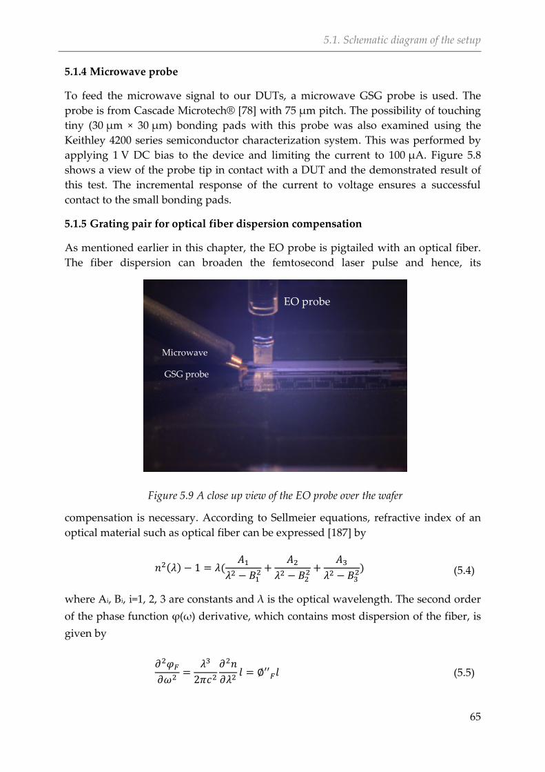
5.1. Schematic diagram of the setup
65
Microwave probe 5.1.4
To feed the microwave signal to our DUTs, a microwave GSG probe is used. The
probe is from Cascade Microtech® [78] with 75 μm pitch. The possibility of touching
tiny (30 µm × 30 µm) bonding pads with this probe was also examined using the
Keithley 4200 series semiconductor characterization system. This was performed by
applying 1 V DC bias to the device and limiting the current to 100 µA. Figure 5.8
shows a view of the probe tip in contact with a DUT and the demonstrated result of
this test. The incremental response of the current to voltage ensures a successful
contact to the small bonding pads.
Grating pair for optical fiber dispersion compensation 5.1.5
As mentioned earlier in this chapter, the EO probe is pigtailed with an optical fiber.
The fiber dispersion can broaden the femtosecond laser pulse and hence, its
compensation is necessary. According to Sellmeier equations, refractive index of an
optical material such as optical fiber can be expressed [187] by
( ) (
) (5.4)
where Ai, Bi, i=1, 2, 3 are constants and λ is the optical wavelength. The second order
of the phase function ϕ(ω) derivative, which contains most dispersion of the fiber, is
given by
(5.5)
EO probe
Microwave
GSG probe
Figure 5.9 A close up view of the EO probe over the wafer
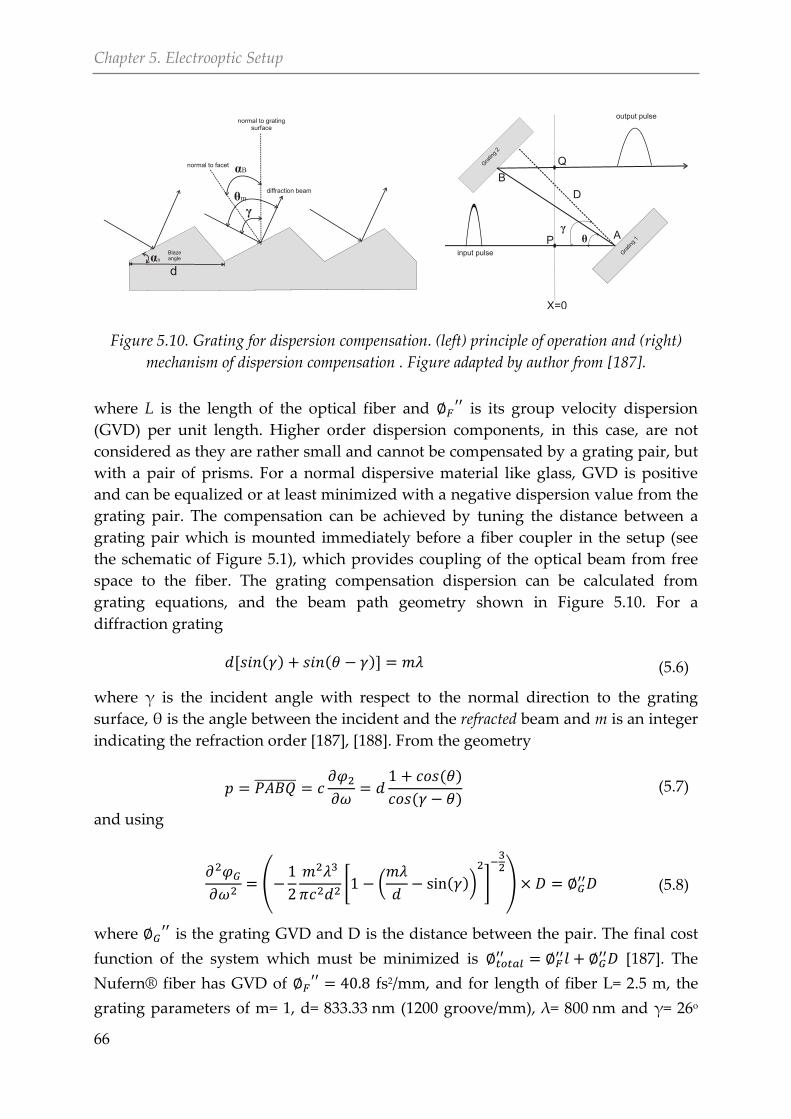
Chapter 5. Electrooptic Setup
66
where L is the length of the optical fiber and is its group velocity dispersion
(GVD) per unit length. Higher order dispersion components, in this case, are not
considered as they are rather small and cannot be compensated by a grating pair, but
with a pair of prisms. For a normal dispersive material like glass, GVD is positive
and can be equalized or at least minimized with a negative dispersion value from the
grating pair. The compensation can be achieved by tuning the distance between a
grating pair which is mounted immediately before a fiber coupler in the setup (see
the schematic of Figure 5.1), which provides coupling of the optical beam from free
space to the fiber. The grating compensation dispersion can be calculated from
grating equations, and the beam path geometry shown in Figure 5.10. For a
diffraction grating
[ ( ) ( )] (5.6)
where γ is the incident angle with respect to the normal direction to the grating
surface, θ is the angle between the incident and the refracted beam and m is an integer
indicating the refraction order [187], [188]. From the geometry
( )
( ) (5.7)
and using
(
[ (
( ))
]
) (5.8)
where is the grating GVD and D is the distance between the pair. The final cost
function of the system which must be minimized is
[187]. The
Nufern® fiber has GVD of fs2/mm, and for length of fiber L= 2.5 m, the
grating parameters of m= 1, d= 833.33 nm (1200 groove/mm), λ= 800 nm and γ= 26o
αB
αB
γ
θm
d
normal to grating surface
normal to facet
Blaze angle
diffraction beamD
γθ
input pulse Gra
ting
1
Gra
ting
2
P
Q
B
A
X=0
output pulse
Figure 5.10. Grating for dispersion compensation. (left) principle of operation and (right)
mechanism of dispersion compensation . Figure adapted by author from [187].
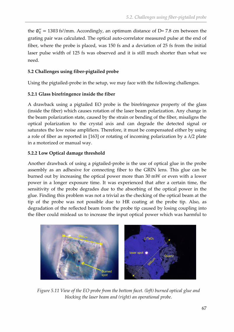
5.2. Challenges using fiber-pigtailed probe
67
the fs2/mm. Accordingly, an optimum distance of D= 7.8 cm between the
grating pair was calculated. The optical auto-correlator measured pulse at the end of
fiber, where the probe is placed, was 150 fs and a deviation of 25 fs from the initial
laser pulse width of 125 fs was observed and it is still much shorter than what we
need.
5.2 Challenges using fiber-pigtailed probe
Using the pigtailed-probe in the setup, we may face with the following challenges.
Glass birefringence inside the fiber 5.2.1
A drawback using a pigtailed EO probe is the birefringence property of the glass
(inside the fiber) which causes rotation of the laser beam polarization. Any change in
the beam polarization state, caused by the strain or bending of the fiber, misaligns the
optical polarization to the crystal axis and can degrade the detected signal or
saturates the low noise amplifiers. Therefore, it must be compensated either by using
a role of fiber as reported in [163] or rotating of incoming polarization by a λ/2 plate
in a motorized or manual way.
Low Optical damage threshold 5.2.2
Another drawback of using a pigtailed-probe is the use of optical glue in the probe
assembly as an adhesive for connecting fiber to the GRIN lens. This glue can be
burned out by increasing the optical power more than 30 mW or even with a lower
power in a longer exposure time. It was experienced that after a certain time, the
sensitivity of the probe degrades due to the absorbing of the optical power in the
glue. Finding this problem was not a trivial as the checking of the optical beam at the
tip of the probe was not possible due to HR coating at the probe tip. Also, as
degradation of the reflected beam from the probe tip caused by losing coupling into
the fiber could mislead us to increase the input optical power which was harmful to
Figure 5.11 View of the EO probe from the bottom facet. (left) burned optical glue and
blocking the laser beam and (right) an operational probe.
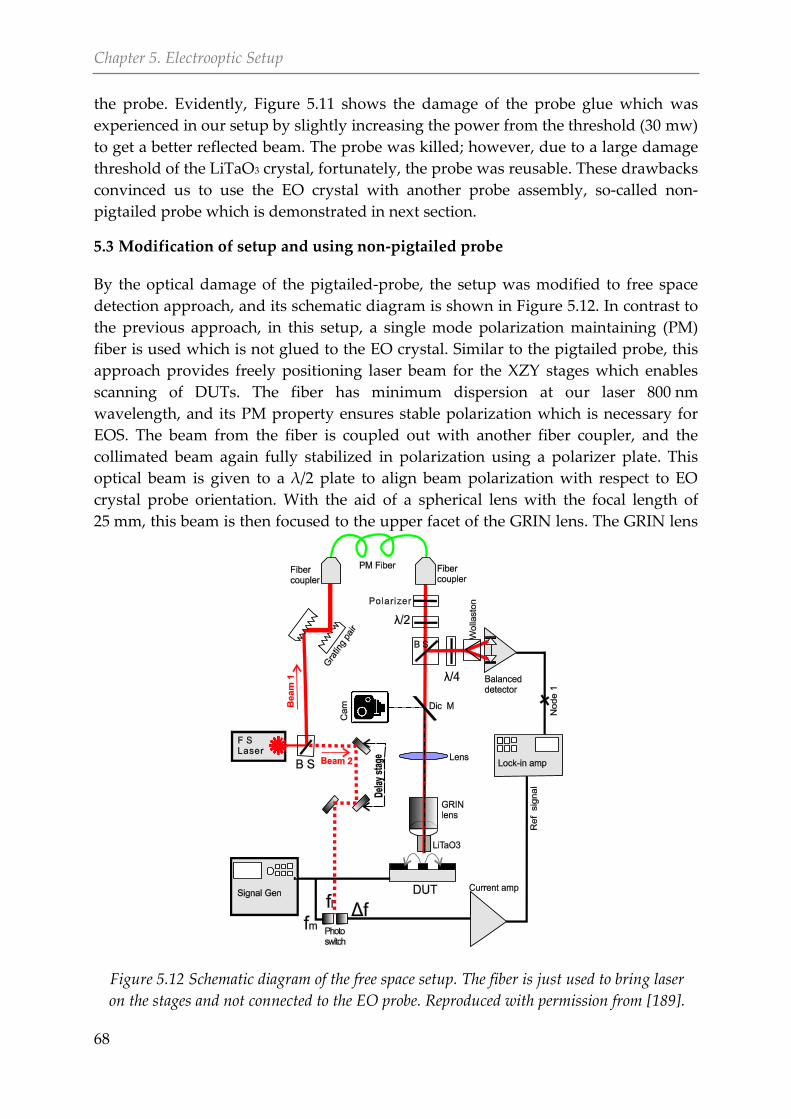
Chapter 5. Electrooptic Setup
68
the probe. Evidently, Figure 5.11 shows the damage of the probe glue which was
experienced in our setup by slightly increasing the power from the threshold (30 mw)
to get a better reflected beam. The probe was killed; however, due to a large damage
threshold of the LiTaO3 crystal, fortunately, the probe was reusable. These drawbacks
convinced us to use the EO crystal with another probe assembly, so-called non-
pigtailed probe which is demonstrated in next section.
5.3 Modification of setup and using non-pigtailed probe
By the optical damage of the pigtailed-probe, the setup was modified to free space
detection approach, and its schematic diagram is shown in Figure 5.12. In contrast to
the previous approach, in this setup, a single mode polarization maintaining (PM)
fiber is used which is not glued to the EO crystal. Similar to the pigtailed probe, this
approach provides freely positioning laser beam for the XZY stages which enables
scanning of DUTs. The fiber has minimum dispersion at our laser 800 nm
wavelength, and its PM property ensures stable polarization which is necessary for
EOS. The beam from the fiber is coupled out with another fiber coupler, and the
collimated beam again fully stabilized in polarization using a polarizer plate. This
optical beam is given to a λ/2 plate to align beam polarization with respect to EO
crystal probe orientation. With the aid of a spherical lens with the focal length of
25 mm, this beam is then focused to the upper facet of the GRIN lens. The GRIN lens
Figure 5.12 Schematic diagram of the free space setup. The fiber is just used to bring laser
on the stages and not connected to the EO probe. Reproduced with permission from [189].
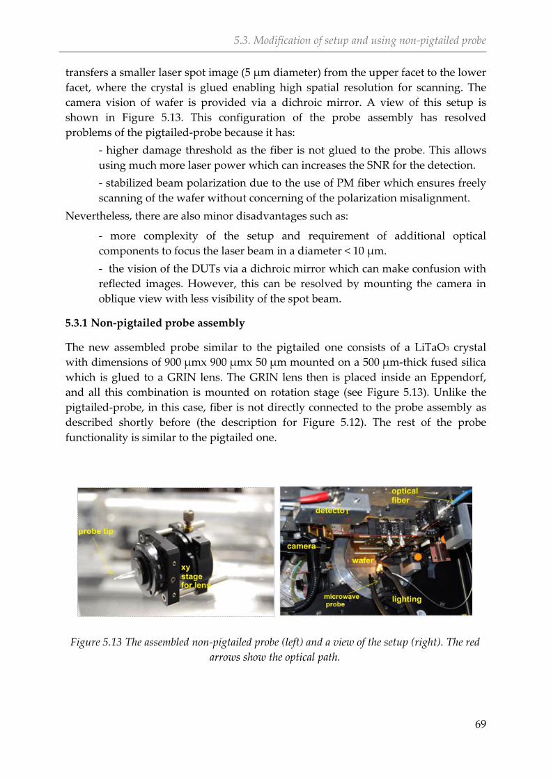
5.3. Modification of setup and using non-pigtailed probe
69
transfers a smaller laser spot image (5 μm diameter) from the upper facet to the lower
facet, where the crystal is glued enabling high spatial resolution for scanning. The
camera vision of wafer is provided via a dichroic mirror. A view of this setup is
shown in Figure 5.13. This configuration of the probe assembly has resolved
problems of the pigtailed-probe because it has:
- higher damage threshold as the fiber is not glued to the probe. This allows
using much more laser power which can increases the SNR for the detection.
- stabilized beam polarization due to the use of PM fiber which ensures freely
scanning of the wafer without concerning of the polarization misalignment.
Nevertheless, there are also minor disadvantages such as:
- more complexity of the setup and requirement of additional optical
components to focus the laser beam in a diameter < 10 μm.
- the vision of the DUTs via a dichroic mirror which can make confusion with
reflected images. However, this can be resolved by mounting the camera in
oblique view with less visibility of the spot beam.[189]
Non-pigtailed probe assembly 5.3.1
The new assembled probe similar to the pigtailed one consists of a LiTaO3 crystal
with dimensions of 900 µmx 900 µmx 50 µm mounted on a 500 µm-thick fused silica
which is glued to a GRIN lens. The GRIN lens then is placed inside an Eppendorf,
and all this combination is mounted on rotation stage (see Figure 5.13). Unlike the
pigtailed-probe, in this case, fiber is not directly connected to the probe assembly as
described shortly before (the description for Figure 5.12). The rest of the probe
functionality is similar to the pigtailed one.
Figure 5.13 The assembled non-pigtailed probe (left) and a view of the setup (right). The red
arrows show the optical path.
r
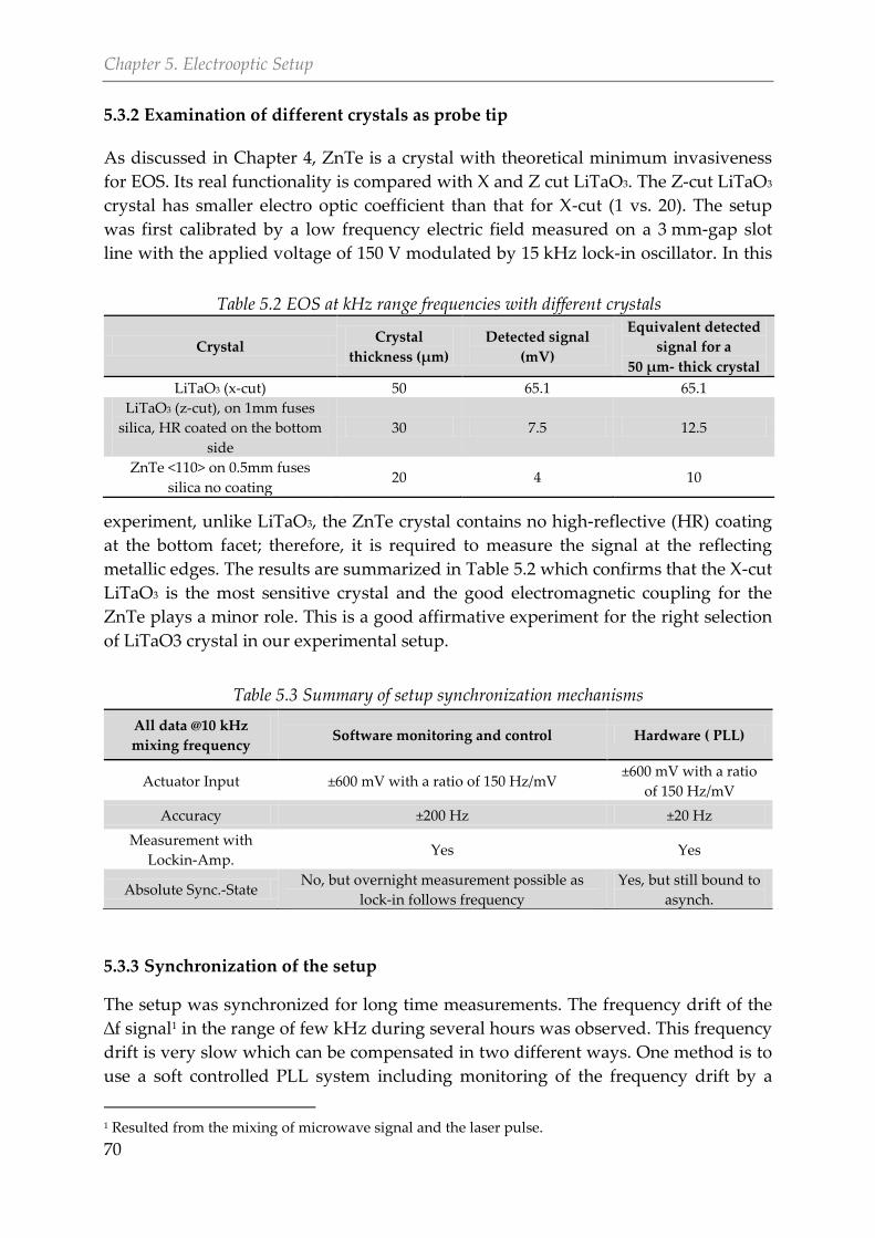
Chapter 5. Electrooptic Setup
70
Examination of different crystals as probe tip 5.3.2
As discussed in Chapter 4, ZnTe is a crystal with theoretical minimum invasiveness
for EOS. Its real functionality is compared with X and Z cut LiTaO3. The Z-cut LiTaO3
crystal has smaller electro optic coefficient than that for X-cut (1 vs. 20). The setup
was first calibrated by a low frequency electric field measured on a 3 mm-gap slot
line with the applied voltage of 150 V modulated by 15 kHz lock-in oscillator. In this
experiment, unlike LiTaO3, the ZnTe crystal contains no high-reflective (HR) coating
at the bottom facet; therefore, it is required to measure the signal at the reflecting
metallic edges. The results are summarized in Table 5.2 which confirms that the X-cut
LiTaO3 is the most sensitive crystal and the good electromagnetic coupling for the
ZnTe plays a minor role. This is a good affirmative experiment for the right selection
of LiTaO3 crystal in our experimental setup.
Synchronization of the setup 5.3.3
The setup was synchronized for long time measurements. The frequency drift of the
∆f signal1 in the range of few kHz during several hours was observed. This frequency
drift is very slow which can be compensated in two different ways. One method is to
use a soft controlled PLL system including monitoring of the frequency drift by a
1 Resulted from the mixing of microwave signal and the laser pulse.
Table 5.2 EOS at kHz range frequencies with different crystals
Crystal Crystal
thickness (μm)
Detected signal
(mV)
Equivalent detected
signal for a
50 μm- thick crystal
LiTaO3 (x-cut) 50 65.1 65.1
LiTaO3 (z-cut), on 1mm fuses
silica, HR coated on the bottom
side
30 7.5 12.5
ZnTe <110> on 0.5mm fuses
silica no coating 20 4 10
Table 5.3 Summary of setup synchronization mechanisms
All data @10 kHz
mixing frequency Software monitoring and control Hardware ( PLL)
Actuator Input ±600 mV with a ratio of 150 Hz/mV ±600 mV with a ratio
of 150 Hz/mV
Accuracy ±200 Hz ±20 Hz
Measurement with
Lockin-Amp. Yes Yes
Absolute Sync.-State No, but overnight measurement possible as
lock-in follows frequency
Yes, but still bound to
asynch.
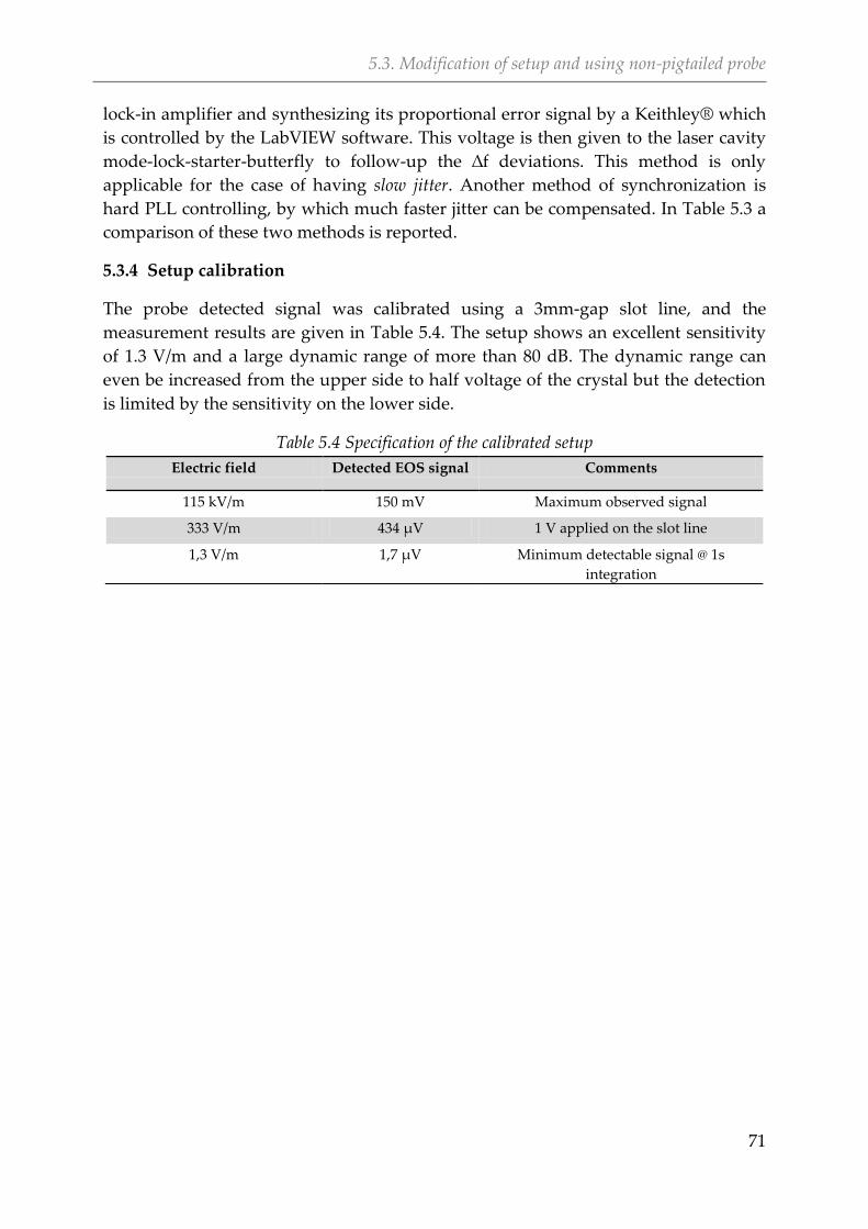
5.3. Modification of setup and using non-pigtailed probe
71
lock-in amplifier and synthesizing its proportional error signal by a Keithley® which
is controlled by the LabVIEW software. This voltage is then given to the laser cavity
mode-lock-starter-butterfly to follow-up the ∆f deviations. This method is only
applicable for the case of having slow jitter. Another method of synchronization is
hard PLL controlling, by which much faster jitter can be compensated. In Table 5.3 a
comparison of these two methods is reported.
Setup calibration 5.3.4
The probe detected signal was calibrated using a 3mm-gap slot line, and the
measurement results are given in Table 5.4. The setup shows an excellent sensitivity
of 1.3 V/m and a large dynamic range of more than 80 dB. The dynamic range can
even be increased from the upper side to half voltage of the crystal but the detection
is limited by the sensitivity on the lower side.
Table 5.4 Specification of the calibrated setup
Electric field Detected EOS signal Comments
115 kV/m 150 mV Maximum observed signal
333 V/m 434 µV 1 V applied on the slot line
1,3 V/m 1,7 µV Minimum detectable signal @ 1s
integration

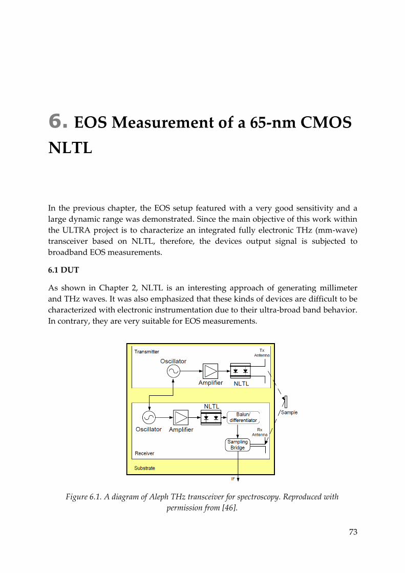
73
EOS Measurement of a 65-nm CMOS 6.
NLTL
In the previous chapter, the EOS setup featured with a very good sensitivity and a
large dynamic range was demonstrated. Since the main objective of this work within
the ULTRA project is to characterize an integrated fully electronic THz (mm-wave)
transceiver based on NLTL, therefore, the devices output signal is subjected to
broadband EOS measurements.
6.1 DUT
As shown in Chapter 2, NLTL is an interesting approach of generating millimeter
and THz waves. It was also emphasized that these kinds of devices are difficult to be
characterized with electronic instrumentation due to their ultra-broad band behavior.
In contrary, they are very suitable for EOS measurements.
Figure 6.1. A diagram of Aleph THz transceiver for spectroscopy. Reproduced with
permission from [46].
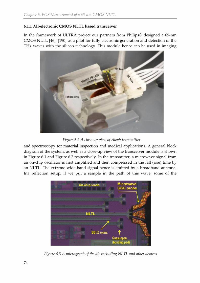
Chapter 6. EOS Measurement of a 65-nm CMOS NLTL
74
All-electronic CMOS NLTL based transceiver 6.1.1
In the framework of ULTRA project our partners from Philips® designed a 65-nm
CMOS NLTL [46], [190] as a pilot for fully electronic generation and detection of the
THz waves with the silicon technology. This module hence can be used in imaging
and spectroscopy for material inspection and medical applications. A general block
diagram of the system, as well as a close-up view of the transceiver module is shown
in Figure 6.1 and Figure 6.2 respectively. In the transmitter, a microwave signal from
an on-chip oscillator is first amplified and then compressed in the fall (rise) time by
an NLTL. The extreme wide-band signal hence is emitted by a broadband antenna.
Ina reflection setup, if we put a sample in the path of this wave, some of the
Figure 6.3 A micrograph of the die including NLTL and other devices
Figure 6.2 A close-up view of Aleph transmitter
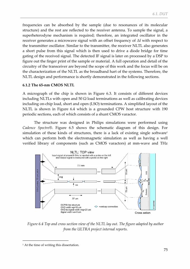
6.1. DUT
75
frequencies can be absorbed by the sample (due to resonances of its molecular
structure) and the rest are reflected to the receiver antenna. To sample the signal, a
superheterodyne mechanism is required; therefore, an integrated oscillator in the
receiver generates a microwave signal with an offset frequency of Δf with respect to
the transmitter oscillator. Similar to the transmitter, the receiver NLTL also generates
a short pulse from this signal which is then used to drive a diode bridge for time
gating of the received signal. The detected IF signal is later on processed by a DSP to
figure out the finger print of the sample or material. A full operation and detail of the
circuitry of the transceiver are beyond the scope of this work and the focus will be on
the characterization of the NLTL as the broadband hart of the systems. Therefore, the
NLTL design and performance is shortly demonstrated in the following sections.
The 65-nm CMOS NLTL 6.1.2
A micrograph of the chip is shown in Figure 6.3. It consists of different devices
including NLTLs with open and 50 Ω load terminations as well as calibrating devices
including on-chip load, short and open (LSO) terminations. A simplified layout of the
NLTL is shown in Figure 6.4 which is a grounded CPW host structure with 190
periodic sections, each of which consists of a shunt CMOS varactor.
The structure was designed in Philips simulations were performed using
Cadence Spectre®. Figure 6.5 shows the schematic diagram of this design. For
simulation of these kinds of structures, there is a lack of existing single software1
which can perform both the electromagnetic simulation as well as having a well
verified library of components (such as CMOS varactors) at mm-wave and THz
1 At the time of writing this dissertation.
Figure 6.4 Top and cross section view of the NLTL lay out. The figure adapted by author
from the ULTRA project internal reports.
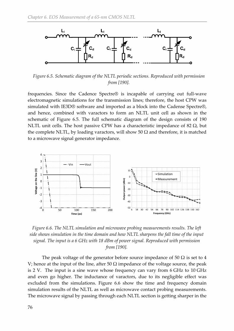
Chapter 6. EOS Measurement of a 65-nm CMOS NLTL
76
frequencies. Since the Cadence Spectre® is incapable of carrying out full-wave
electromagnetic simulations for the transmission lines; therefore, the host CPW was
simulated with IE3D® software and imported as a block into the Cadense Spectre®,
and hence, combined with varactors to form an NLTL unit cell as shown in the
schematic of Figure 6.5. The full schematic diagram of the design consists of 190
NLTL unit cells. The host passive CPW has a characteristic impedance of 82 Ω, but
the complete NLTL, by loading varactors, will show 50 Ω and therefore, it is matched
to a microwave signal generator impedance.
The peak voltage of the generator before source impedance of 50 Ω is set to 4
V; hence at the input of the line, after 50 Ω impedance of the voltage source, the peak
is 2 V. The input is a sine wave whose frequency can vary from 6 GHz to 10 GHz
and even go higher. The inductance of varactors, due to its negligible effect was
excluded from the simulations. Figure 6.6 show the time and frequency domain
simulation results of the NLTL as well as microwave contact probing measurements.
The microwave signal by passing through each NLTL section is getting sharper in the
Figure 6.5. Schematic diagram of the NLTL periodic sections. Reproduced with permission
from [190].
Figure 6.6. The NLTL simulation and microwave probing measurements results. The left
side shows simulation in the time domain and how NLTL sharpens the fall time of the input
signal. The input is a 6 GHz with 18 dBm of power signal. Reproduced with permission
from [190].
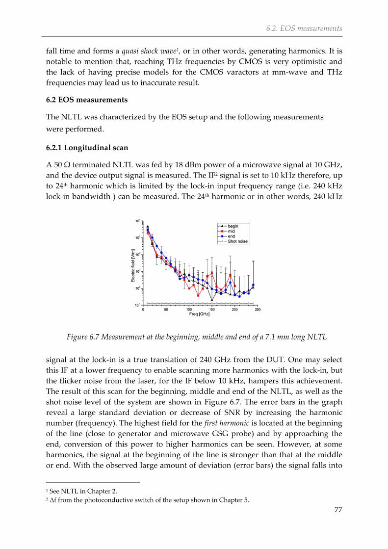
6.2. EOS measurements
77
fall time and forms a quasi shock wave1, or in other words, generating harmonics. It is
notable to mention that, reaching THz frequencies by CMOS is very optimistic and
the lack of having precise models for the CMOS varactors at mm-wave and THz
frequencies may lead us to inaccurate result.
6.2 EOS measurements
The NLTL was characterized by the EOS setup and the following measurements
were performed.
Longitudinal scan 6.2.1
A 50 Ω terminated NLTL was fed by 18 dBm power of a microwave signal at 10 GHz,
and the device output signal is measured. The IF2 signal is set to 10 kHz therefore, up
to 24th harmonic which is limited by the lock-in input frequency range (i.e. 240 kHz
lock-in bandwidth ) can be measured. The 24th harmonic or in other words, 240 kHz
signal at the lock-in is a true translation of 240 GHz from the DUT. One may select
this IF at a lower frequency to enable scanning more harmonics with the lock-in, but
the flicker noise from the laser, for the IF below 10 kHz, hampers this achievement.
The result of this scan for the beginning, middle and end of the NLTL, as well as the
shot noise level of the system are shown in Figure 6.7. The error bars in the graph
reveal a large standard deviation or decrease of SNR by increasing the harmonic
number (frequency). The highest field for the first harmonic is located at the beginning
of the line (close to generator and microwave GSG probe) and by approaching the
end, conversion of this power to higher harmonics can be seen. However, at some
harmonics, the signal at the beginning of the line is stronger than that at the middle
or end. With the observed large amount of deviation (error bars) the signal falls into
1 See NLTL in Chapter 2. 2 Δf from the photoconductive switch of the setup shown in Chapter 5.
Figure 6.7 Measurement at the beginning, middle and end of a 7.1 mm long NLTL
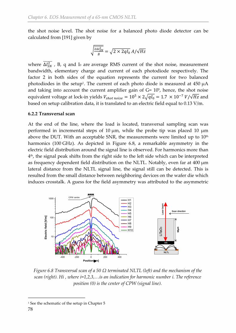
Chapter 6. EOS Measurement of a 65-nm CMOS NLTL
78
the shot noise level. The shot noise for a balanced photo diode detector can be
calculated from [191] given by
√
√ √
where , B, q and I0 are average RMS current of the shot noise, measurement
bandwidth, elementary charge and current of each photodiode respectively. The
factor 2 in both sides of the equation represents the current for two balanced
photodiodes in the setup1. The current of each photo diode is measured at 450 µA
and taking into account the current amplifier gain of G= 105, hence, the shot noise
equivalent voltage at lock-in yields √ √ and
based on setup calibration data, it is translated to an electric field equal to 0.13 V/m.
Transversal scan 6.2.2
At the end of the line, where the load is located, transversal sampling scan was
performed in incremental steps of 10 µm, while the probe tip was placed 10 μm
above the DUT. With an acceptable SNR, the measurements were limited up to 10th
harmonics (100 GHz). As depicted in Figure 6.8, a remarkable asymmetry in the
electric field distribution around the signal line is observed. For harmonics more than
4th, the signal peak shifts from the right side to the left side which can be interpreted
as frequency dependent field distribution on the NLTL. Notably, even far at 400 μm
lateral distance from the NLTL signal line, the signal still can be detected. This is
resulted from the small distance between neighboring devices on the wafer die which
induces crosstalk. A guess for the field asymmetry was attributed to the asymmetric
1 See the schematic of the setup in Chapter 5
-400 -200 0 200 400
10
100
1000
Ele
ctr
ic f
ield
[V
/m]
Position[m]
H1
H2
H3
H4
H5
H6
H7
H8
H9
H10
CPW centre
Figure 6.8 Transversal scan of a 50 Ω terminated NLTL (left) and the mechanism of the
scan (right). Hi , where i=1,2,3,…is an indication for harmonic number i. The reference
position (0) is the center of CPW (signal line).
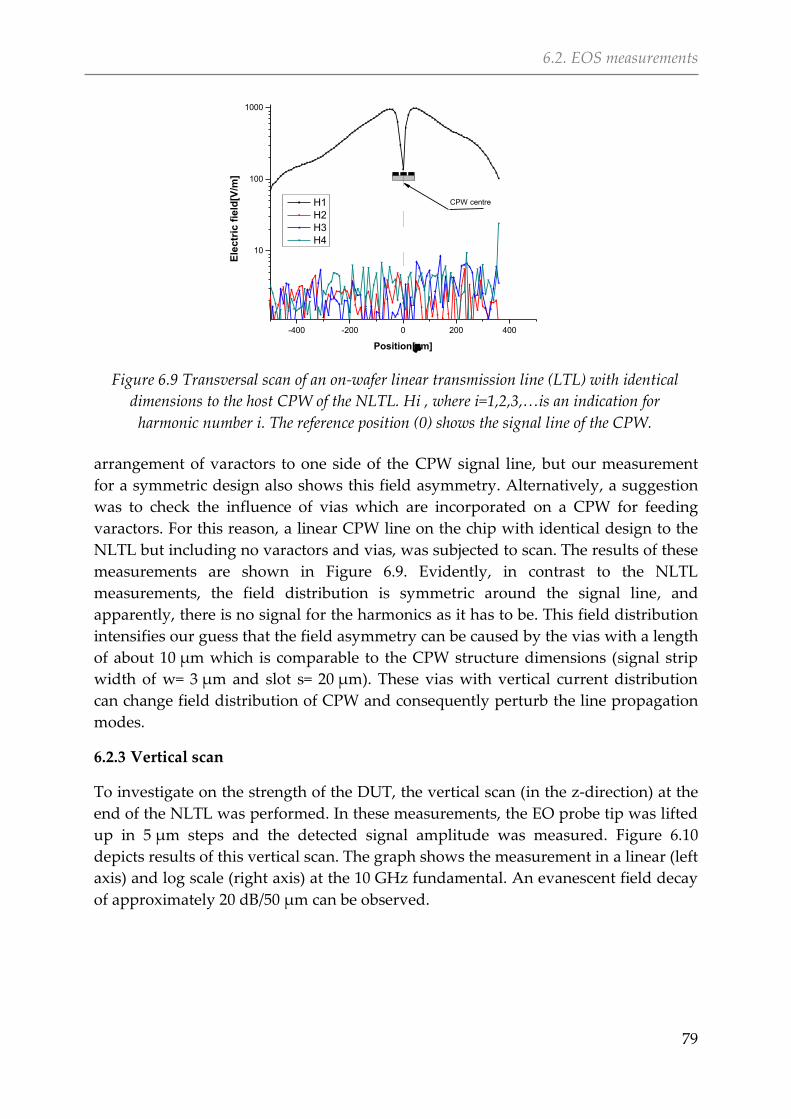
6.2. EOS measurements
79
arrangement of varactors to one side of the CPW signal line, but our measurement
for a symmetric design also shows this field asymmetry. Alternatively, a suggestion
was to check the influence of vias which are incorporated on a CPW for feeding
varactors. For this reason, a linear CPW line on the chip with identical design to the
NLTL but including no varactors and vias, was subjected to scan. The results of these
measurements are shown in Figure 6.9. Evidently, in contrast to the NLTL
measurements, the field distribution is symmetric around the signal line, and
apparently, there is no signal for the harmonics as it has to be. This field distribution
intensifies our guess that the field asymmetry can be caused by the vias with a length
of about 10 µm which is comparable to the CPW structure dimensions (signal strip
width of w= 3 µm and slot s= 20 µm). These vias with vertical current distribution
can change field distribution of CPW and consequently perturb the line propagation
modes.
Vertical scan 6.2.3
To investigate on the strength of the DUT, the vertical scan (in the z-direction) at the
end of the NLTL was performed. In these measurements, the EO probe tip was lifted
up in 5 µm steps and the detected signal amplitude was measured. Figure 6.10
depicts results of this vertical scan. The graph shows the measurement in a linear (left
axis) and log scale (right axis) at the 10 GHz fundamental. An evanescent field decay
of approximately 20 dB/50 μm can be observed.
-400 -200 0 200 400
10
100
1000
Ele
ctr
ic f
ield
[V/m
]
Position[m]
H1
H2
H3
H4
CPW centre
Figure 6.9 Transversal scan of an on-wafer linear transmission line (LTL) with identical
dimensions to the host CPW of the NLTL. Hi , where i=1,2,3,…is an indication for
harmonic number i. The reference position (0) shows the signal line of the CPW.
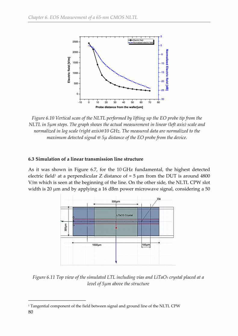
Chapter 6. EOS Measurement of a 65-nm CMOS NLTL
80
6.3 Simulation of a linear transmission line structure
As it was shown in Figure 6.7, for the 10 GHz fundamental, the highest detected
electric field1 at a perpendicular Z distance of ≈ 5 μm from the DUT is around 4800
V/m which is seen at the beginning of the line. On the other side, the NLTL CPW slot
width is 20 μm and by applying a 16 dBm power microwave signal, considering a 50
1 Tangential component of the field between signal and ground line of the NLTL CPW
Figure 6.10 Vertical scan of the NLTL performed by lifting up the EO probe tip from the
NLTL in 5µm steps. The graph shows the actual measurement in linear (left axis) scale and
normalized in log scale (right axis)@10 GHz. The measured data are normalized to the
maximum detected signal @ 5µ distance of the EO probe from the device.
Figure 6.11 Top view of the simulated LTL including vias and LiTaO3 crystal placed at a
level of 5µm above the structure
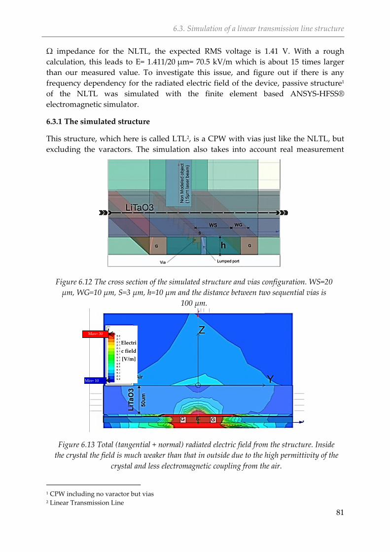
6.3. Simulation of a linear transmission line structure
81
Ω impedance for the NLTL, the expected RMS voltage is 1.41 V. With a rough
calculation, this leads to E= 1.411/20 μm= 70.5 kV/m which is about 15 times larger
than our measured value. To investigate this issue, and figure out if there is any
frequency dependency for the radiated electric field of the device, passive structure1
of the NLTL was simulated with the finite element based ANSYS-HFSS®
electromagnetic simulator.
The simulated structure 6.3.1
This structure, which here is called LTL2, is a CPW with vias just like the NLTL, but
excluding the varactors. The simulation also takes into account real measurement
1 CPW including no varactor but vias 2 Linear Transmission Line
Figure 6.12 The cross section of the simulated structure and vias configuration. WS=20
µm, WG=10 µm, S=3 µm, h=10 µm and the distance between two sequential vias is
100 µm.
Figure 6.13 Total (tangential + normal) radiated electric field from the structure. Inside
the crystal the field is much weaker than that in outside due to the high permittivity of the
crystal and less electromagnetic coupling from the air.
Max= 30
kV/m
Min= 10
V/m
Electri
c field
[V/m]
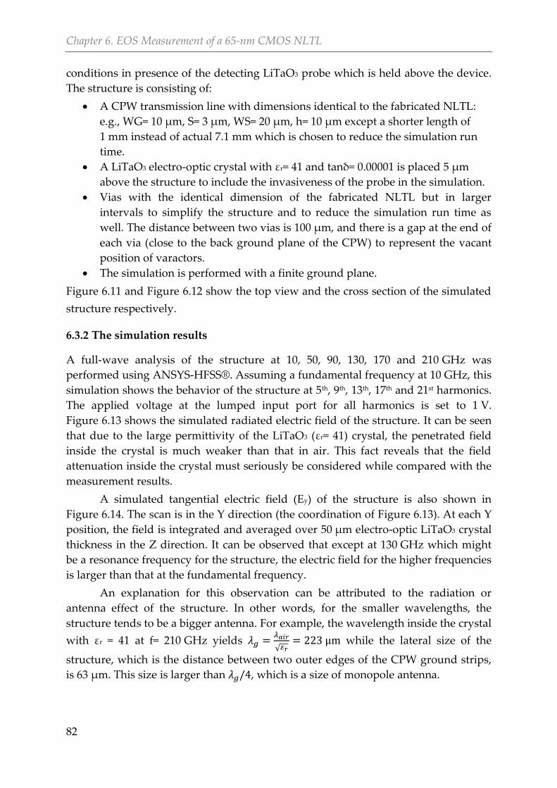
Chapter 6. EOS Measurement of a 65-nm CMOS NLTL
82
conditions in presence of the detecting LiTaO3 probe which is held above the device.
The structure is consisting of:
A CPW transmission line with dimensions identical to the fabricated NLTL:
e.g., WG= 10 µm, S= 3 µm, WS= 20 µm, h= 10 µm except a shorter length of
1 mm instead of actual 7.1 mm which is chosen to reduce the simulation run
time.
A LiTaO3 electro-optic crystal with εr= 41 and tanδ= 0.00001 is placed 5 µm
above the structure to include the invasiveness of the probe in the simulation.
Vias with the identical dimension of the fabricated NLTL but in larger
intervals to simplify the structure and to reduce the simulation run time as
well. The distance between two vias is 100 µm, and there is a gap at the end of
each via (close to the back ground plane of the CPW) to represent the vacant
position of varactors.
The simulation is performed with a finite ground plane.
Figure 6.11 and Figure 6.12 show the top view and the cross section of the simulated
structure respectively.
The simulation results 6.3.2
A full-wave analysis of the structure at 10, 50, 90, 130, 170 and 210 GHz was
performed using ANSYS-HFSS®. Assuming a fundamental frequency at 10 GHz, this
simulation shows the behavior of the structure at 5th, 9th, 13th, 17th and 21st harmonics.
The applied voltage at the lumped input port for all harmonics is set to 1 V.
Figure 6.13 shows the simulated radiated electric field of the structure. It can be seen
that due to the large permittivity of the LiTaO3 (εr= 41) crystal, the penetrated field
inside the crystal is much weaker than that in air. This fact reveals that the field
attenuation inside the crystal must seriously be considered while compared with the
measurement results.
A simulated tangential electric field (Ey) of the structure is also shown in
Figure 6.14. The scan is in the Y direction (the coordination of Figure 6.13). At each Y
position, the field is integrated and averaged over 50 µm electro-optic LiTaO3 crystal
thickness in the Z direction. It can be observed that except at 130 GHz which might
be a resonance frequency for the structure, the electric field for the higher frequencies
is larger than that at the fundamental frequency.
An explanation for this observation can be attributed to the radiation or
antenna effect of the structure. In other words, for the smaller wavelengths, the
structure tends to be a bigger antenna. For example, the wavelength inside the crystal
with εr = 41 at f= 210 GHz yields
√ while the lateral size of the
structure, which is the distance between two outer edges of the CPW ground strips,
is 63 µm. This size is larger than , which is a size of monopole antenna.
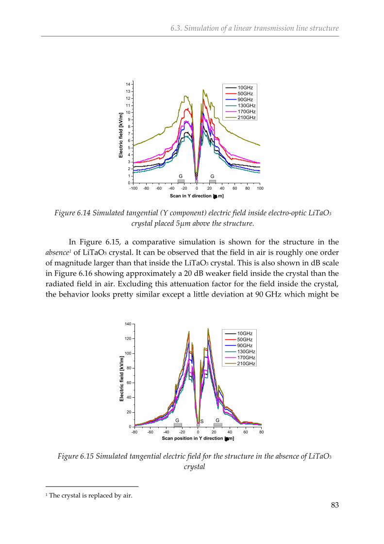
6.3. Simulation of a linear transmission line structure
83
In Figure 6.15, a comparative simulation is shown for the structure in the
absence1 of LiTaO3 crystal. It can be observed that the field in air is roughly one order
of magnitude larger than that inside the LiTaO3 crystal. This is also shown in dB scale
in Figure 6.16 showing approximately a 20 dB weaker field inside the crystal than the
radiated field in air. Excluding this attenuation factor for the field inside the crystal,
the behavior looks pretty similar except a little deviation at 90 GHz which might be
1 The crystal is replaced by air.
-100 -80 -60 -40 -20 0 20 40 60 80 100
0
1
2
3
4
5
6
7
8
9
10
11
12
13
14
G S
Ele
ctr
ic f
ield
[k
V/m
]
Scan in Y direction [m]
10GHz
50GHz
90GHz
130GHz
170GHz
210GHz
G
Figure 6.14 Simulated tangential (Y component) electric field inside electro-optic LiTaO3
crystal placed 5µm above the structure.
-80 -60 -40 -20 0 20 40 60 80
0
20
40
60
80
100
120
140
Ele
ctr
ic f
ield
[k
V/m
]
Scan position in Y direction [m]
10GHz
50GHz
90GHz
130GHz
170GHz
210GHz
G S G
Figure 6.15 Simulated tangential electric field for the structure in the absence of LiTaO3
crystal
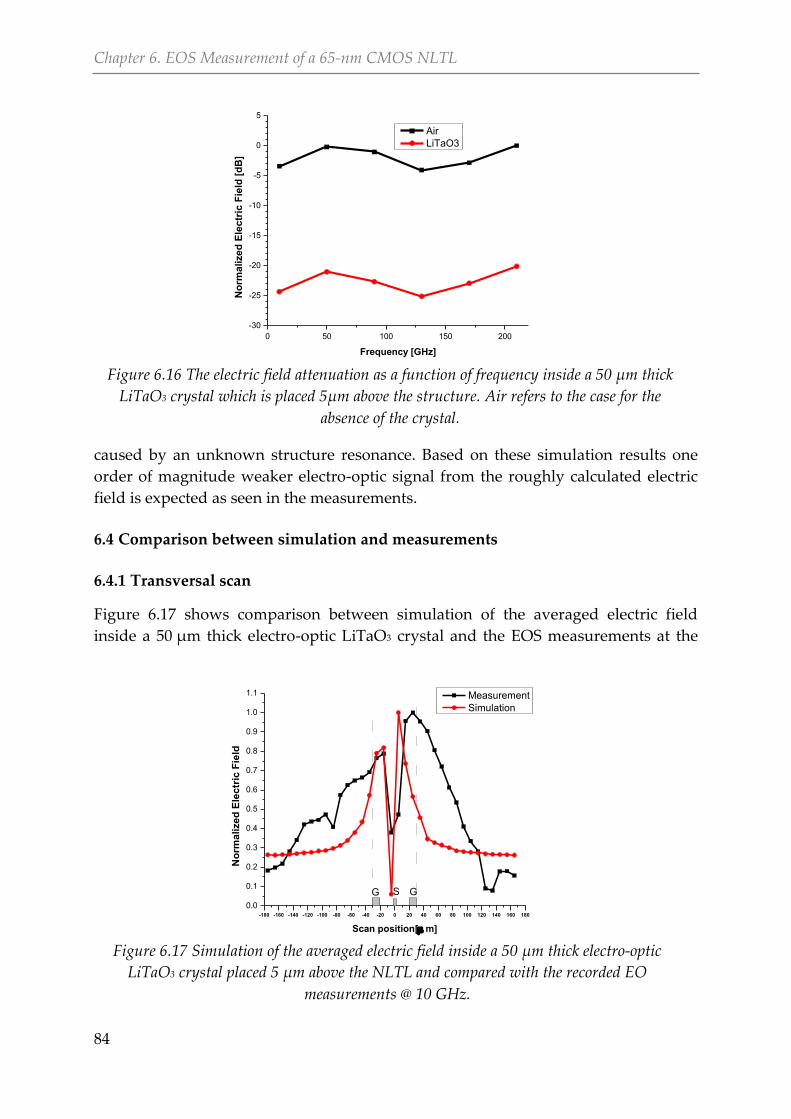
Chapter 6. EOS Measurement of a 65-nm CMOS NLTL
84
caused by an unknown structure resonance. Based on these simulation results one
order of magnitude weaker electro-optic signal from the roughly calculated electric
field is expected as seen in the measurements.
6.4 Comparison between simulation and measurements
Transversal scan 6.4.1
Figure 6.17 shows comparison between simulation of the averaged electric field
inside a 50 µm thick electro-optic LiTaO3 crystal and the EOS measurements at the
0 50 100 150 200
-30
-25
-20
-15
-10
-5
0
5
No
rma
lize
d E
lec
tric
Fie
ld [
dB
]
Frequency [GHz]
Air
LiTaO3
Figure 6.16 The electric field attenuation as a function of frequency inside a 50 µm thick
LiTaO3 crystal which is placed 5µm above the structure. Air refers to the case for the
absence of the crystal.
-180 -160 -140 -120 -100 -80 -60 -40 -20 0 20 40 60 80 100 120 140 160 180
0.0
0.1
0.2
0.3
0.4
0.5
0.6
0.7
0.8
0.9
1.0
1.1
SG
No
rma
lize
d E
lec
tric
Fie
ld
Scan position[m]
Measurement
Simulation
G
Figure 6.17 Simulation of the averaged electric field inside a 50 µm thick electro-optic
LiTaO3 crystal placed 5 µm above the NLTL and compared with the recorded EO
measurements @ 10 GHz.
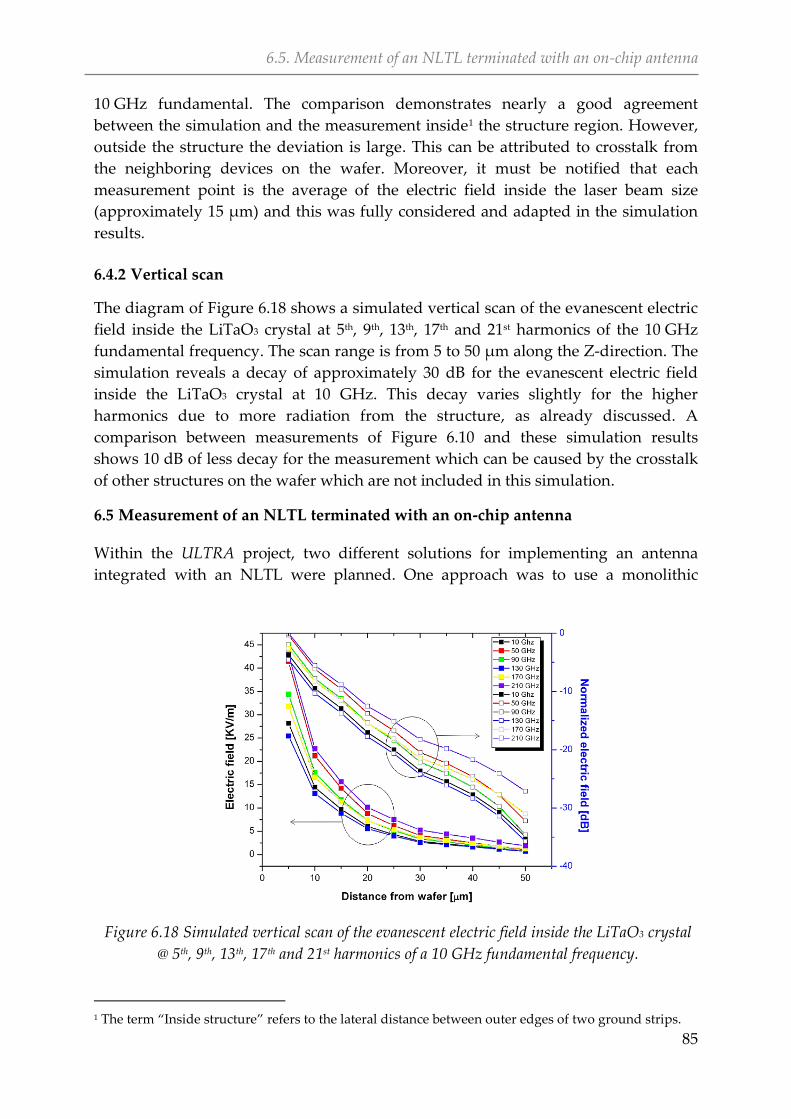
6.5. Measurement of an NLTL terminated with an on-chip antenna
85
10 GHz fundamental. The comparison demonstrates nearly a good agreement
between the simulation and the measurement inside1 the structure region. However,
outside the structure the deviation is large. This can be attributed to crosstalk from
the neighboring devices on the wafer. Moreover, it must be notified that each
measurement point is the average of the electric field inside the laser beam size
(approximately 15 μm) and this was fully considered and adapted in the simulation
results.
Vertical scan 6.4.2
The diagram of Figure 6.18 shows a simulated vertical scan of the evanescent electric
field inside the LiTaO3 crystal at 5th, 9th, 13th, 17th and 21st harmonics of the 10 GHz
fundamental frequency. The scan range is from 5 to 50 µm along the Z-direction. The
simulation reveals a decay of approximately 30 dB for the evanescent electric field
inside the LiTaO3 crystal at 10 GHz. This decay varies slightly for the higher
harmonics due to more radiation from the structure, as already discussed. A
comparison between measurements of Figure 6.10 and these simulation results
shows 10 dB of less decay for the measurement which can be caused by the crosstalk
of other structures on the wafer which are not included in this simulation.
6.5 Measurement of an NLTL terminated with an on-chip antenna
Within the ULTRA project, two different solutions for implementing an antenna
integrated with an NLTL were planned. One approach was to use a monolithic
1 The term “Inside structure” refers to the lateral distance between outer edges of two ground strips.
Figure 6.18 Simulated vertical scan of the evanescent electric field inside the LiTaO3 crystal
@ 5th, 9th, 13th, 17th and 21st harmonics of a 10 GHz fundamental frequency.
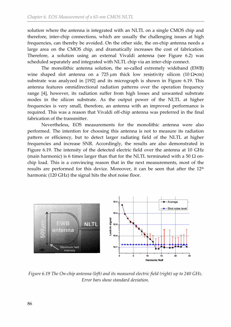
Chapter 6. EOS Measurement of a 65-nm CMOS NLTL
86
solution where the antenna is integrated with an NLTL on a single CMOS chip and
therefore, inter-chip connections, which are usually the challenging issues at high
frequencies, can thereby be avoided. On the other side, the on-chip antenna needs a
large area on the CMOS chip, and dramatically increases the cost of fabrication.
Therefore, a solution using an external Vivaldi antenna (see Figure 6.2) was
scheduled separately and integrated with NLTL chip via an inter-chip connect.
The monolithic antenna solution, the so-called extremely wideband (EWB)
wine shaped slot antenna on a 725 μm thick low resistivity silicon (10 Ωcm)
substrate was analyzed in [192] and its micrograph is shown in Figure 6.19. This
antenna features omnidirectional radiation patterns over the operation frequency
range [4], however, its radiation suffer from high losses and unwanted substrate
modes in the silicon substrate. As the output power of the NLTL at higher
frequencies is very small, therefore, an antenna with an improved performance is
required. This was a reason that Vivaldi off-chip antenna was preferred in the final
fabrication of the transmitter.
Nevertheless, EOS measurements for the monolithic antenna were also
performed. The intention for choosing this antenna is not to measure its radiation
pattern or efficiency, but to detect larger radiating field of the NLTL at higher
frequencies and increase SNR. Accordingly, the results are also demonstrated in
Figure 6.19. The intensity of the detected electric field over the antenna at 10 GHz
(main harmonic) is 6 times larger than that for the NLTL terminated with a 50 Ω on-
chip load. This is a convincing reason that in the next measurements, most of the
results are performed for this device. Moreover, it can be seen that after the 12th
harmonic (120 GHz) the signal hits the shot noise floor.
Figure 6.19 The On-chip antenna (left) and its measured electric field (right) up to 240 GHz.
Error bars show standard deviation.
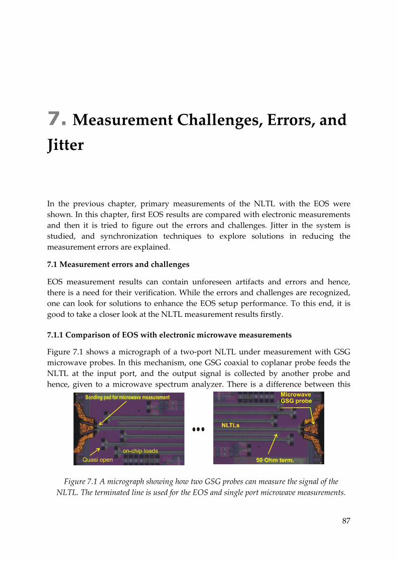
87
Measurement Challenges, Errors, and 7.
Jitter
In the previous chapter, primary measurements of the NLTL with the EOS were
shown. In this chapter, first EOS results are compared with electronic measurements
and then it is tried to figure out the errors and challenges. Jitter in the system is
studied, and synchronization techniques to explore solutions in reducing the
measurement errors are explained.
7.1 Measurement errors and challenges
EOS measurement results can contain unforeseen artifacts and errors and hence,
there is a need for their verification. While the errors and challenges are recognized,
one can look for solutions to enhance the EOS setup performance. To this end, it is
good to take a closer look at the NLTL measurement results firstly.
Comparison of EOS with electronic microwave measurements 7.1.1
Figure 7.1 shows a micrograph of a two-port NLTL under measurement with GSG
microwave probes. In this mechanism, one GSG coaxial to coplanar probe feeds the
NLTL at the input port, and the output signal is collected by another probe and
hence, given to a microwave spectrum analyzer. There is a difference between this
Figure 7.1 A micrograph showing how two GSG probes can measure the signal of the
NLTL. The terminated line is used for the EOS and single port microwave measurements.
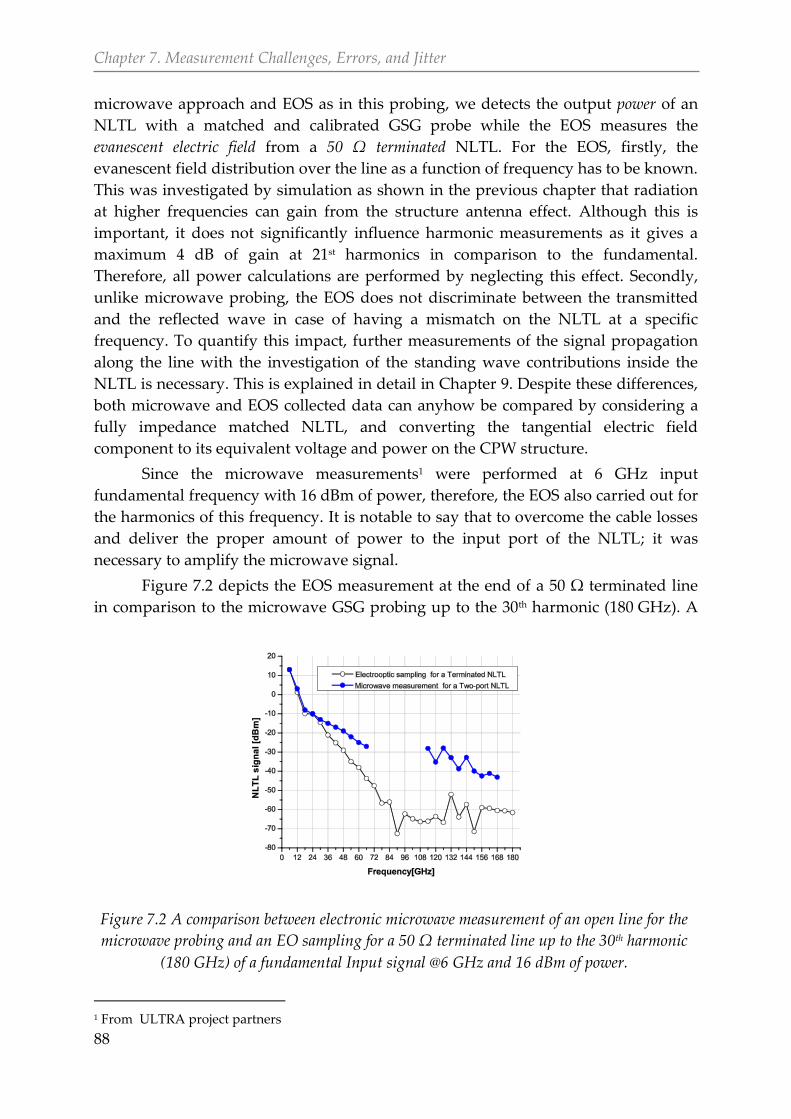
Chapter 7. Measurement Challenges, Errors, and Jitter
88
microwave approach and EOS as in this probing, we detects the output power of an
NLTL with a matched and calibrated GSG probe while the EOS measures the
evanescent electric field from a 50 Ω terminated NLTL. For the EOS, firstly, the
evanescent field distribution over the line as a function of frequency has to be known.
This was investigated by simulation as shown in the previous chapter that radiation
at higher frequencies can gain from the structure antenna effect. Although this is
important, it does not significantly influence harmonic measurements as it gives a
maximum 4 dB of gain at 21st harmonics in comparison to the fundamental.
Therefore, all power calculations are performed by neglecting this effect. Secondly,
unlike microwave probing, the EOS does not discriminate between the transmitted
and the reflected wave in case of having a mismatch on the NLTL at a specific
frequency. To quantify this impact, further measurements of the signal propagation
along the line with the investigation of the standing wave contributions inside the
NLTL is necessary. This is explained in detail in Chapter 9. Despite these differences,
both microwave and EOS collected data can anyhow be compared by considering a
fully impedance matched NLTL, and converting the tangential electric field
component to its equivalent voltage and power on the CPW structure.
Since the microwave measurements1 were performed at 6 GHz input
fundamental frequency with 16 dBm of power, therefore, the EOS also carried out for
the harmonics of this frequency. It is notable to say that to overcome the cable losses
and deliver the proper amount of power to the input port of the NLTL; it was
necessary to amplify the microwave signal.
Figure 7.2 depicts the EOS measurement at the end of a 50 Ω terminated line
in comparison to the microwave GSG probing up to the 30th harmonic (180 GHz). A
1 From ULTRA project partners
Figure 7.2 A comparison between electronic microwave measurement of an open line for the
microwave probing and an EO sampling for a 50 Ω terminated line up to the 30th harmonic
(180 GHz) of a fundamental Input signal @6 GHz and 16 dBm of power.
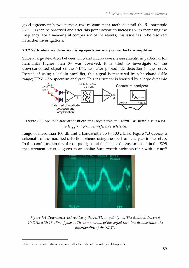
7.1. Measurement errors and challenges
89
good agreement between these two measurement methods until the 5th harmonic
(30 GHz) can be observed and after this point deviation increases with increasing the
frequency. For a meaningful comparison of the results, this issue has to be resolved
in further investigations.
Self-reference detection using spectrum analyzer vs. lock-in amplifier 7.1.2
Since a large deviation between EOS and microwave measurements, in particular for
harmonics higher than 5th was observed, it is tried to investigate on the
downconverted signal of the NLTL i.e., after photodiode detection in the setup.
Instead of using a lock-in amplifier, this signal is measured by a baseband (kHz
range) HP35665A spectrum analyzer. This instrument is featured by a large dynamic
range of more than 100 dB and a bandwidth up to 100.2 kHz. Figure 7.3 depicts a
schematic of the modified detection scheme using the spectrum analyzer in the setup.
In this configuration first the output signal of the balanced detector1, used in the EOS
measurement setup, is given to an analog Butterworth highpass filter with a cutoff
1 For more detail of detection, see full schematic of the setup in Chapter 5.
+
-Input Trigger
20-40dB
Balanced photodiode detection and amplification
Spectrum analyzerHigh Pass filter
fc=3.5 kHzLaser beam
1 2
Figure 7.3 Schematic diagram of spectrum analyzer detection setup. The signal also is used
as trigger to form self-reference detection.
Figure 7.4 Downconverted replica of the NLTL output signal. The device is driven @
10 GHz with 18 dBm of power. The compression of the signal rise time demonstrates the
functionality of the NLTL.
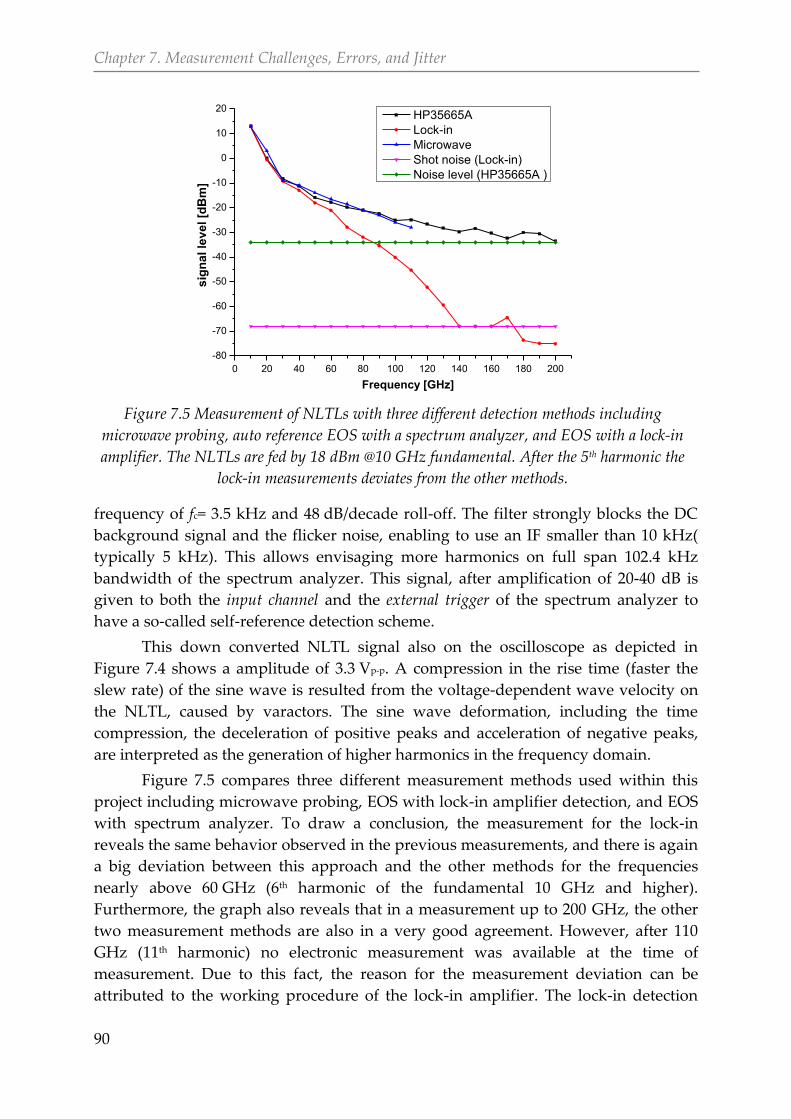
Chapter 7. Measurement Challenges, Errors, and Jitter
90
frequency of fc= 3.5 kHz and 48 dB/decade roll-off. The filter strongly blocks the DC
background signal and the flicker noise, enabling to use an IF smaller than 10 kHz(
typically 5 kHz). This allows envisaging more harmonics on full span 102.4 kHz
bandwidth of the spectrum analyzer. This signal, after amplification of 20-40 dB is
given to both the input channel and the external trigger of the spectrum analyzer to
have a so-called self-reference detection scheme.
This down converted NLTL signal also on the oscilloscope as depicted in
Figure 7.4 shows a amplitude of 3.3 Vp-p. A compression in the rise time (faster the
slew rate) of the sine wave is resulted from the voltage-dependent wave velocity on
the NLTL, caused by varactors. The sine wave deformation, including the time
compression, the deceleration of positive peaks and acceleration of negative peaks,
are interpreted as the generation of higher harmonics in the frequency domain.
Figure 7.5 compares three different measurement methods used within this
project including microwave probing, EOS with lock-in amplifier detection, and EOS
with spectrum analyzer. To draw a conclusion, the measurement for the lock-in
reveals the same behavior observed in the previous measurements, and there is again
a big deviation between this approach and the other methods for the frequencies
nearly above 60 GHz (6th harmonic of the fundamental 10 GHz and higher).
Furthermore, the graph also reveals that in a measurement up to 200 GHz, the other
two measurement methods are also in a very good agreement. However, after 110
GHz (11th harmonic) no electronic measurement was available at the time of
measurement. Due to this fact, the reason for the measurement deviation can be
attributed to the working procedure of the lock-in amplifier. The lock-in detection
0 20 40 60 80 100 120 140 160 180 200
-80
-70
-60
-50
-40
-30
-20
-10
0
10
20
sig
na
l le
ve
l [d
Bm
]
Frequency [GHz]
HP35665A
Lock-in
Microwave
Shot noise (Lock-in)
Noise level (HP35665A )
Figure 7.5 Measurement of NLTLs with three different detection methods including
microwave probing, auto reference EOS with a spectrum analyzer, and EOS with a lock-in
amplifier. The NLTLs are fed by 18 dBm @10 GHz fundamental. After the 5th harmonic the
lock-in measurements deviates from the other methods.
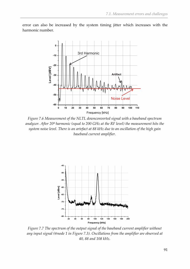
7.1. Measurement errors and challenges
91
error can also be increased by the system timing jitter which increases with the
harmonic number.
20 40 60 80 100 120 140 160 180 200
-80
-75
-70
-65
-60
-55
-50
-45
Le
ve
l [d
Bm
]
Frequency [kHz]
Figure 7.7 The spectrum of the output signal of the baseband current amplifier without
any input signal (@node 1 in Figure 7.3). Oscillations from the amplifier are observed at
40, 88 and 108 kHz.
0 10 20 30 40 50 60 70 80 90 100 110
-60
-50
-40
-30
-20
-10
0
Le
ve
l[d
BV
]
Frequency [kHz]
3rd Harmonic
Noise Level
Artifact
Figure 7.6 Measurement of the NLTL downconverted signal with a baseband spectrum
analyzer. After 20th harmonic (equal to 200 GHz at the RF level) the measurement hits the
system noise level. There is an artefact at 88 kHz due to an oscillation of the high gain
baseband current amplifier.
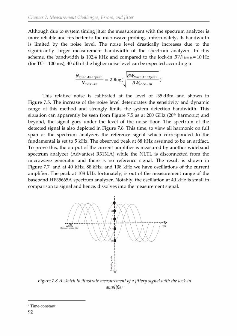
Chapter 7. Measurement Challenges, Errors, and Jitter
92
Although due to system timing jitter the measurement with the spectrum analyzer is
more reliable and fits better to the microwave probing, unfortunately, its bandwidth
is limited by the noise level. The noise level drastically increases due to the
significantly larger measurement bandwidth of the spectrum analyzer. In this
scheme, the bandwidth is 102.4 kHz and compared to the lock-in BW|lock-in = 10 Hz
(for TC1= 100 ms), 40 dB of the higher noise level can be expected according to
(√
)
This relative noise is calibrated at the level of -35 dBm and shown in
Figure 7.5. The increase of the noise level deteriorates the sensitivity and dynamic
range of this method and strongly limits the system detection bandwidth. This
situation can apparently be seen from Figure 7.5 as at 200 GHz (20th harmonic) and
beyond, the signal goes under the level of the noise floor. The spectrum of the
detected signal is also depicted in Figure 7.6. This time, to view all harmonic on full
span of the spectrum analyzer, the reference signal which corresponded to the
fundamental is set to 5 kHz. The observed peak at 88 kHz assumed to be an artifact.
To prove this, the output of the current amplifier is measured by another wideband
spectrum analyzer (Advantest R3131A) while the NLTL is disconnected from the
microwave generator and there is no reference signal. The result is shown in
Figure 7.7, and at 40 kHz, 88 kHz, and 108 kHz we have oscillations of the current
amplifier. The peak at 108 kHz fortunately, is out of the measurement range of the
baseband HP35665A spectrum analyzer. Notably, the oscillation at 40 kHz is small in
comparison to signal and hence, dissolves into the measurement signal.
1 Time-constant
1
2
n-1
n
Random phase jitter
J(t) t[S]
Sam
plin
g s
hots
Figure 7.8 A sketch to illustrate measurement of a jittery signal with the lock-in
amplifier
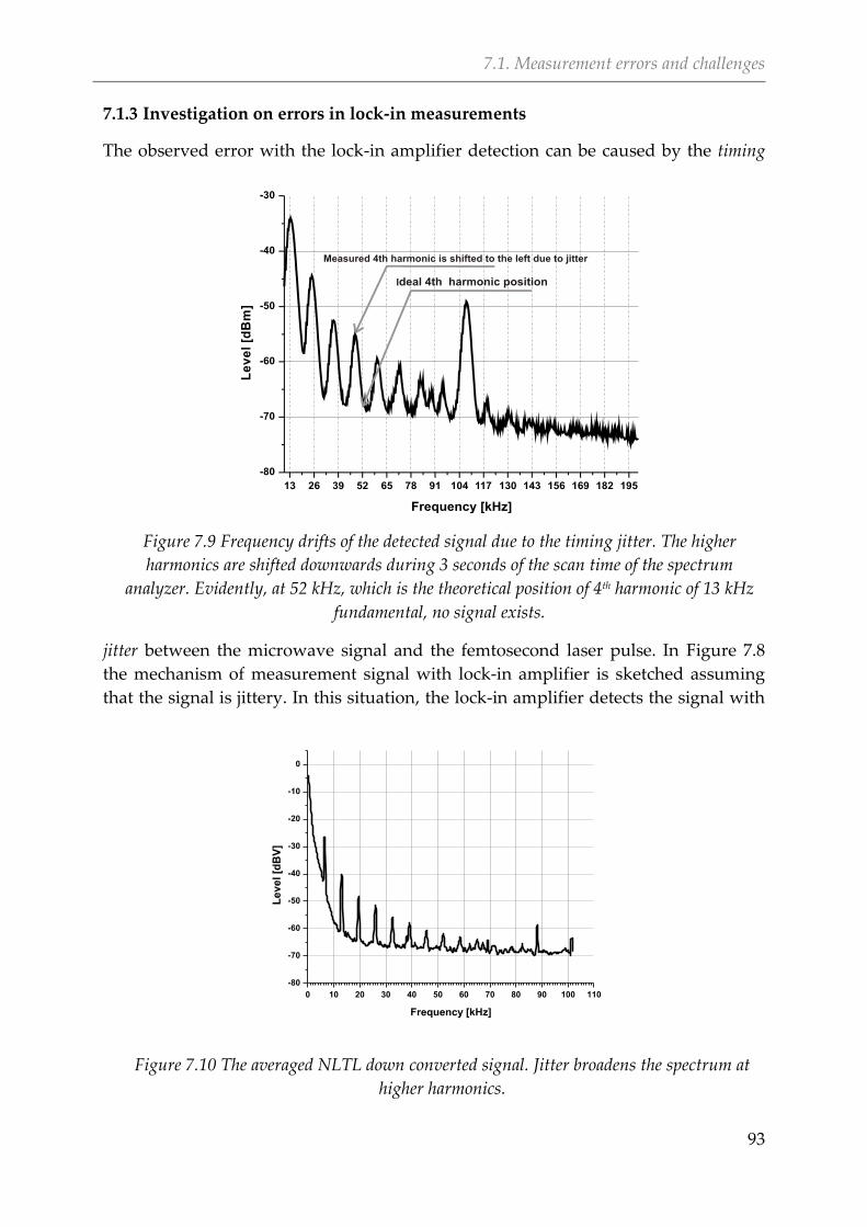
7.1. Measurement errors and challenges
93
Investigation on errors in lock-in measurements 7.1.3
The observed error with the lock-in amplifier detection can be caused by the timing
jitter between the microwave signal and the femtosecond laser pulse. In Figure 7.8
the mechanism of measurement signal with lock-in amplifier is sketched assuming
that the signal is jittery. In this situation, the lock-in amplifier detects the signal with
13 26 39 52 65 78 91 104 117 130 143 156 169 182 195
-80
-70
-60
-50
-40
-30
Le
ve
l[d
Bm
]
Frequency [kHz]
Ideal 4th harmonic position
Measured 4th harmonic is shifted to the left due to jitter
Figure 7.9 Frequency drifts of the detected signal due to the timing jitter. The higher
harmonics are shifted downwards during 3 seconds of the scan time of the spectrum
analyzer. Evidently, at 52 kHz, which is the theoretical position of 4th harmonic of 13 kHz
fundamental, no signal exists.
0 10 20 30 40 50 60 70 80 90 100 110
-80
-70
-60
-50
-40
-30
-20
-10
0
Le
ve
l [d
BV
]
Frequency [kHz]
Figure 7.10 The averaged NLTL down converted signal. Jitter broadens the spectrum at
higher harmonics.
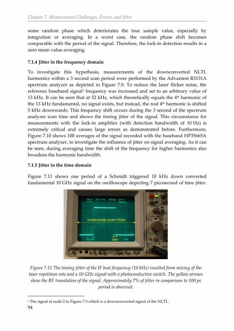
Chapter 7. Measurement Challenges, Errors, and Jitter
94
some random phase which deteriorates the true sample value, especially by
integration or averaging. In a worst case, the random phase shift becomes
comparable with the period of the signal. Therefore, the lock-in detection results in a
zero mean value averaging.
Jitter in the frequency domain 7.1.4
To investigate this hypothesis, measurements of the downconverted NLTL
harmonics within a 3 second scan period were performed by the Advantest R3131A
spectrum analyzer as depicted in Figure 7.9. To reduce the laser flicker noise, the
reference baseband signal1 frequency was increased and set to an arbitrary value of
13 kHz. It can be seen that at 52 kHz, which theoretically equals the 4th harmonic of
the 13 kHz fundamental, no signal exists, but instead, the real 4th harmonic is shifted
5 kHz downwards. This frequency shift occurs during the 3 second of the spectrum
analyzer scan time and shows the timing jitter of the signal. This circumstance for
measurements with the lock-in amplifier (with detection bandwidth of 10 Hz) is
extremely critical and causes large errors as demonstrated before. Furthermore,
Figure 7.10 shows 100 averages of the signal recorded with the baseband HP35665A
spectrum analyzer, to investigate the influence of jitter on signal averaging. As it can
be seen, during averaging time the shift of the frequency for higher harmonics also
broadens the harmonic bandwidth.
Jitter in the time domain 7.1.5
Figure 7.11 shows one period of a Schmidt triggered 10 kHz down converted
fundamental 10 GHz signal on the oscilloscope depicting 7 picosecond of time jitter.
1 The signal at node 2 in Figure 7.3 which is a downconverted signal of the NLTL.
Figure 7.11 The timing jitter of the IF beat frequency (10 kHz) resulted from mixing of the
laser repetition rate and a 10 GHz signal with a photoconductive switch. The yellow arrows
show the RF translation of the signal. Approximately 7% of jitter in comparison to 100 ps
period is observed.
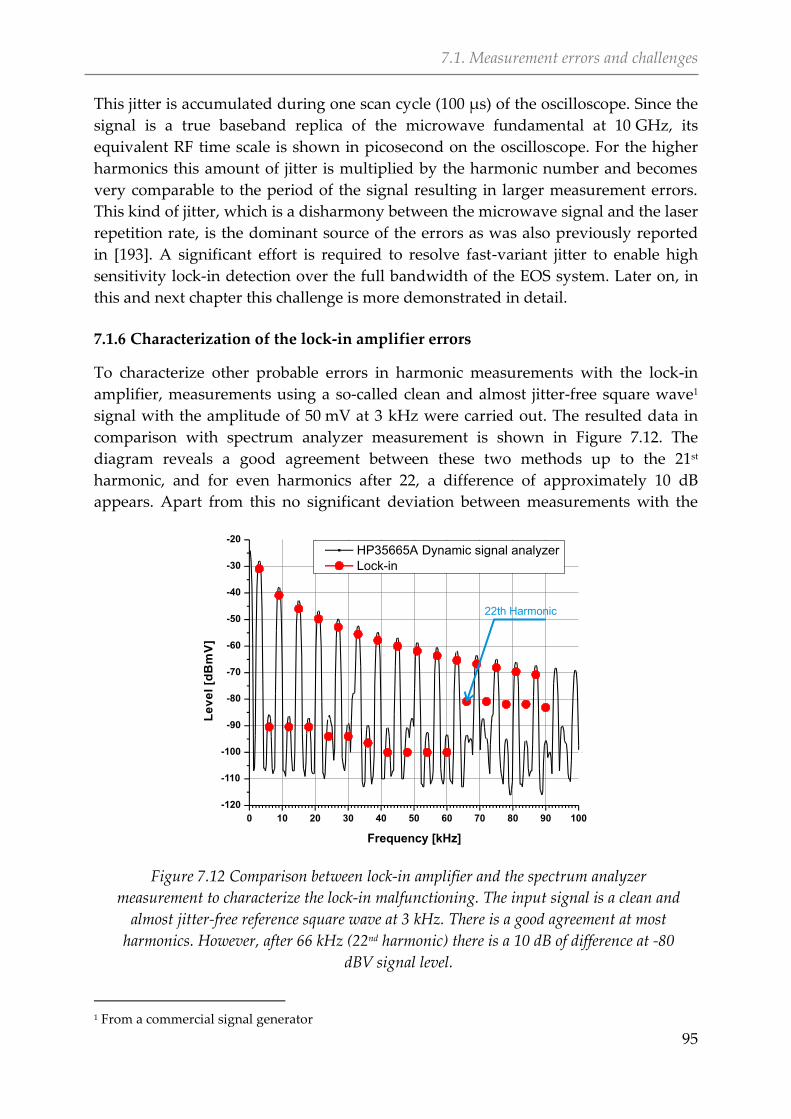
7.1. Measurement errors and challenges
95
This jitter is accumulated during one scan cycle (100 µs) of the oscilloscope. Since the
signal is a true baseband replica of the microwave fundamental at 10 GHz, its
equivalent RF time scale is shown in picosecond on the oscilloscope. For the higher
harmonics this amount of jitter is multiplied by the harmonic number and becomes
very comparable to the period of the signal resulting in larger measurement errors.
This kind of jitter, which is a disharmony between the microwave signal and the laser
repetition rate, is the dominant source of the errors as was also previously reported
in [193]. A significant effort is required to resolve fast-variant jitter to enable high
sensitivity lock-in detection over the full bandwidth of the EOS system. Later on, in
this and next chapter this challenge is more demonstrated in detail.
Characterization of the lock-in amplifier errors 7.1.6
To characterize other probable errors in harmonic measurements with the lock-in
amplifier, measurements using a so-called clean and almost jitter-free square wave1
signal with the amplitude of 50 mV at 3 kHz were carried out. The resulted data in
comparison with spectrum analyzer measurement is shown in Figure 7.12. The
diagram reveals a good agreement between these two methods up to the 21st
harmonic, and for even harmonics after 22, a difference of approximately 10 dB
appears. Apart from this no significant deviation between measurements with the
1 From a commercial signal generator
0 10 20 30 40 50 60 70 80 90 100
-120
-110
-100
-90
-80
-70
-60
-50
-40
-30
-20
Le
ve
l[d
Bm
V]
Frequency [kHz]
HP35665A Dynamic signal analyzer
Lock-in
22th Harmonic
Figure 7.12 Comparison between lock-in amplifier and the spectrum analyzer
measurement to characterize the lock-in malfunctioning. The input signal is a clean and
almost jitter-free reference square wave at 3 kHz. There is a good agreement at most
harmonics. However, after 66 kHz (22nd harmonic) there is a 10 dB of difference at -80
dBV signal level.
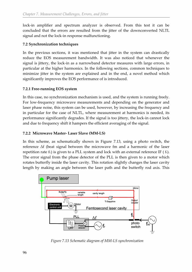
Chapter 7. Measurement Challenges, Errors, and Jitter
96
lock-in amplifier and spectrum analyzer is observed. From this test it can be
concluded that the errors are resulted from the jitter of the downconverted NLTL
signal and not the lock-in response malfunctioning.
7.2 Synchronization techniques
In the previous sections, it was mentioned that jitter in the system can drastically
reduce the EOS measurement bandwidth. It was also noticed that whenever the
signal is jittery, the lock-in as a narrowband detector measures with large errors, in
particular at the higher harmonics. In the following sections, common techniques to
minimize jitter in the system are explained and in the end, a novel method which
significantly improves the EOS performance of is introduced.
Free-running EOS system 7.2.1
In this case, no synchronization mechanism is used, and the system is running freely.
For low-frequency microwave measurements and depending on the generator and
laser phase noise, this system can be used, however, by increasing the frequency and
in particular for the case of NLTL, where measurement at harmonics is needed, its
performance significantly degrades. If the signal is too jittery, the lock-in cannot lock
and due to frequency shift it hampers the efficient averaging of the signal.
Microwave Master- Laser Slave (MM-LS) 7.2.2
In this scheme, as schematically shown in Figure 7.13, using a photo switch, the
reference Δf (beat signal between the microwave fm and a harmonic of the laser
repetition rate fL) is given to a PLL system and lock with an external reference IF ( fr).
The error signal from the phase detector of the PLL is then given to a motor which
rotates butterfly inside the laser cavity. This rotation slightly changes the laser cavity
length by making an angle between the laser path and the butterfly rod axis. This
Figure 7.13 Schematic diagram of MM-LS synchronization
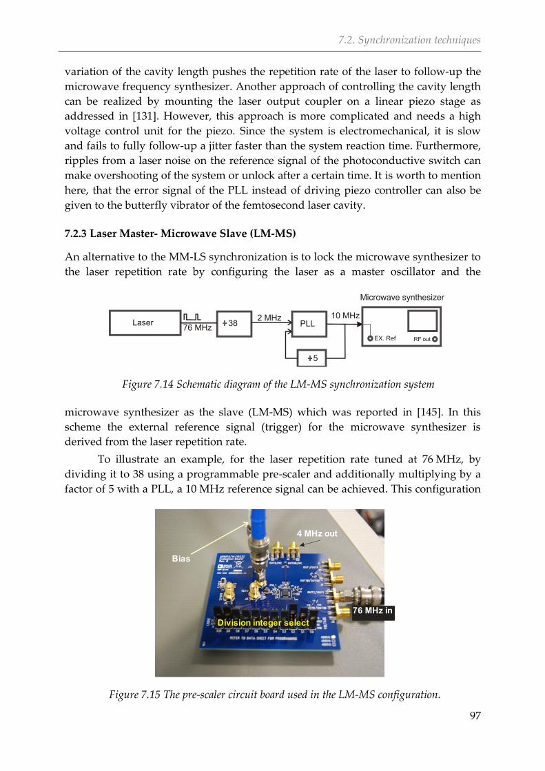
7.2. Synchronization techniques
97
variation of the cavity length pushes the repetition rate of the laser to follow-up the
microwave frequency synthesizer. Another approach of controlling the cavity length
can be realized by mounting the laser output coupler on a linear piezo stage as
addressed in [131]. However, this approach is more complicated and needs a high
voltage control unit for the piezo. Since the system is electromechanical, it is slow
and fails to fully follow-up a jitter faster than the system reaction time. Furthermore,
ripples from a laser noise on the reference signal of the photoconductive switch can
make overshooting of the system or unlock after a certain time. It is worth to mention
here, that the error signal of the PLL instead of driving piezo controller can also be
given to the butterfly vibrator of the femtosecond laser cavity.
Laser Master- Microwave Slave (LM-MS) 7.2.3
An alternative to the MM-LS synchronization is to lock the microwave synthesizer to
the laser repetition rate by configuring the laser as a master oscillator and the
microwave synthesizer as the slave (LM-MS) which was reported in [145]. In this
scheme the external reference signal (trigger) for the microwave synthesizer is
derived from the laser repetition rate.
To illustrate an example, for the laser repetition rate tuned at 76 MHz, by
dividing it to 38 using a programmable pre-scaler and additionally multiplying by a
factor of 5 with a PLL, a 10 MHz reference signal can be achieved. This configuration
4 MHz out
Division integer select
Bias
76 MHz in
Figure 7.15 The pre-scaler circuit board used in the LM-MS configuration.
Laser 38
5
PLL76 MHz
2 MHz 10 MHz
EX. Ref
Microwave synthesizer
RF out
Figure 7.14 Schematic diagram of the LM-MS synchronization system
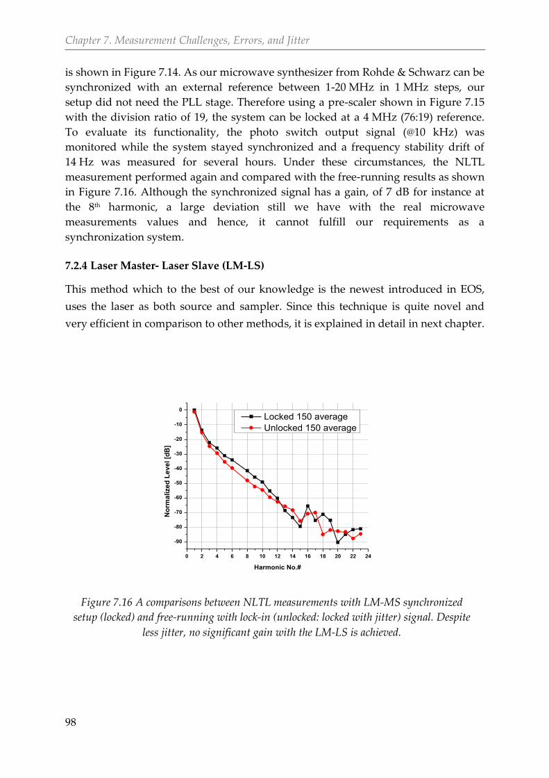
Chapter 7. Measurement Challenges, Errors, and Jitter
98
is shown in Figure 7.14. As our microwave synthesizer from Rohde & Schwarz can be
synchronized with an external reference between 1-20 MHz in 1 MHz steps, our
setup did not need the PLL stage. Therefore using a pre-scaler shown in Figure 7.15
with the division ratio of 19, the system can be locked at a 4 MHz (76:19) reference.
To evaluate its functionality, the photo switch output signal (@10 kHz) was
monitored while the system stayed synchronized and a frequency stability drift of
14 Hz was measured for several hours. Under these circumstances, the NLTL
measurement performed again and compared with the free-running results as shown
in Figure 7.16. Although the synchronized signal has a gain, of 7 dB for instance at
the 8th harmonic, a large deviation still we have with the real microwave
measurements values and hence, it cannot fulfill our requirements as a
synchronization system.
Laser Master- Laser Slave (LM-LS) 7.2.4
This method which to the best of our knowledge is the newest introduced in EOS,
uses the laser as both source and sampler. Since this technique is quite novel and
very efficient in comparison to other methods, it is explained in detail in next chapter.
0 2 4 6 8 10 12 14 16 18 20 22 24
-90
-80
-70
-60
-50
-40
-30
-20
-10
0
No
rma
lize
d L
ev
el [d
B]
Harmonic No.#
Locked 150 average
Unlocked 150 average
Figure 7.16 A comparisons between NLTL measurements with LM-MS synchronized
setup (locked) and free-running with lock-in (unlocked: locked with jitter) signal. Despite
less jitter, no significant gain with the LM-LS is achieved.
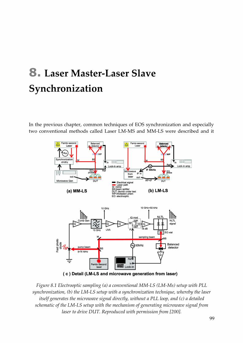
99
Laser Master-Laser Slave 8.
Synchronization
In the previous chapter, common techniques of EOS synchronization and especially
two conventional methods called Laser LM-MS and MM-LS were described and it
Figure 8.1 Electrooptic sampling (a) a conventional MM-LS (LM-Ms) setup with PLL
synchronization, (b) the LM-LS setup with a synchronization technique, whereby the laser
itself generates the microwave signal directly, without a PLL loop, and (c) a detailed
schematic of the LM-LS setup with the mechanism of generating microwave signal from
laser to drive DUT. Reproduced with permission from [200].
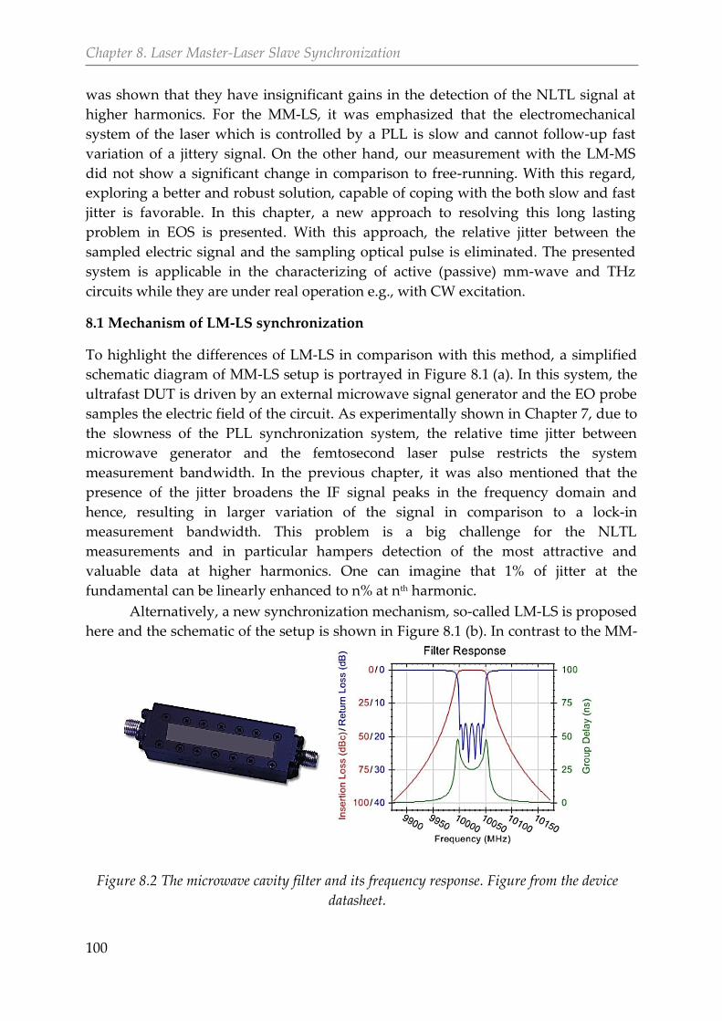
Chapter 8. Laser Master-Laser Slave Synchronization
100
was shown that they have insignificant gains in the detection of the NLTL signal at
higher harmonics. For the MM-LS, it was emphasized that the electromechanical
system of the laser which is controlled by a PLL is slow and cannot follow-up fast
variation of a jittery signal. On the other hand, our measurement with the LM-MS
did not show a significant change in comparison to free-running. With this regard,
exploring a better and robust solution, capable of coping with the both slow and fast
jitter is favorable. In this chapter, a new approach to resolving this long lasting
problem in EOS is presented. With this approach, the relative jitter between the
sampled electric signal and the sampling optical pulse is eliminated. The presented
system is applicable in the characterizing of active (passive) mm-wave and THz
circuits while they are under real operation e.g., with CW excitation.
8.1 Mechanism of LM-LS synchronization
To highlight the differences of LM-LS in comparison with this method, a simplified
schematic diagram of MM-LS setup is portrayed in Figure 8.1 (a). In this system, the
ultrafast DUT is driven by an external microwave signal generator and the EO probe
samples the electric field of the circuit. As experimentally shown in Chapter 7, due to
the slowness of the PLL synchronization system, the relative time jitter between
microwave generator and the femtosecond laser pulse restricts the system
measurement bandwidth. In the previous chapter, it was also mentioned that the
presence of the jitter broadens the IF signal peaks in the frequency domain and
hence, resulting in larger variation of the signal in comparison to a lock-in
measurement bandwidth. This problem is a big challenge for the NLTL
measurements and in particular hampers detection of the most attractive and
valuable data at higher harmonics. One can imagine that 1% of jitter at the
fundamental can be linearly enhanced to n% at nth harmonic.
Alternatively, a new synchronization mechanism, so-called LM-LS is proposed
here and the schematic of the setup is shown in Figure 8.1 (b). In contrast to the MM-
Figure 8.2 The microwave cavity filter and its frequency response. Figure from the device
datasheet.
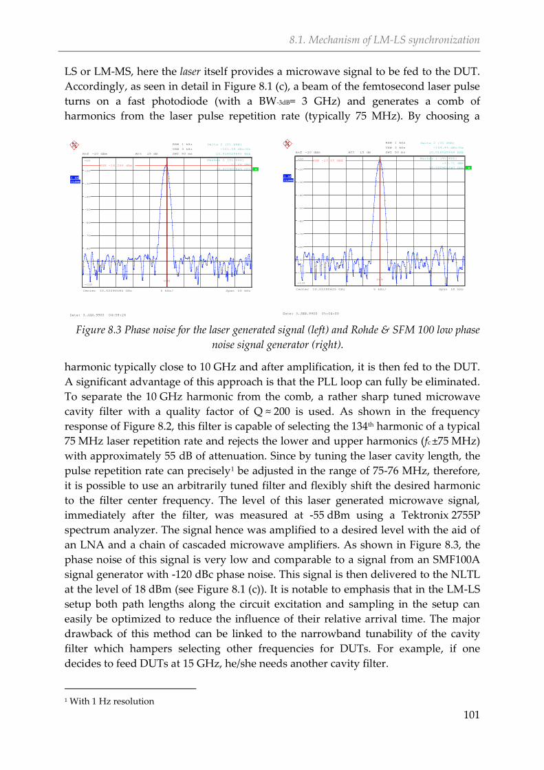
8.1. Mechanism of LM-LS synchronization
101
LS or LM-MS, here the laser itself provides a microwave signal to be fed to the DUT.
Accordingly, as seen in detail in Figure 8.1 (c), a beam of the femtosecond laser pulse
turns on a fast photodiode (with a BW-3dB= 3 GHz) and generates a comb of
harmonics from the laser pulse repetition rate (typically 75 MHz). By choosing a
harmonic typically close to 10 GHz and after amplification, it is then fed to the DUT.
A significant advantage of this approach is that the PLL loop can fully be eliminated.
To separate the 10 GHz harmonic from the comb, a rather sharp tuned microwave
cavity filter with a quality factor of Q ≈ 200 is used. As shown in the frequency
response of Figure 8.2, this filter is capable of selecting the 134th harmonic of a typical
75 MHz laser repetition rate and rejects the lower and upper harmonics (fc ±75 MHz)
with approximately 55 dB of attenuation. Since by tuning the laser cavity length, the
pulse repetition rate can precisely1 be adjusted in the range of 75-76 MHz, therefore,
it is possible to use an arbitrarily tuned filter and flexibly shift the desired harmonic
to the filter center frequency. The level of this laser generated microwave signal,
immediately after the filter, was measured at -55 dBm using a Tektronix 2755P
spectrum analyzer. The signal hence was amplified to a desired level with the aid of
an LNA and a chain of cascaded microwave amplifiers. As shown in Figure 8.3, the
phase noise of this signal is very low and comparable to a signal from an SMF100A
signal generator with -120 dBc phase noise. This signal is then delivered to the NLTL
at the level of 18 dBm (see Figure 8.1 (c)). It is notable to emphasis that in the LM-LS
setup both path lengths along the circuit excitation and sampling in the setup can
easily be optimized to reduce the influence of their relative arrival time. The major
drawback of this method can be linked to the narrowband tunability of the cavity
filter which hampers selecting other frequencies for DUTs. For example, if one
decides to feed DUTs at 15 GHz, he/she needs another cavity filter.
1 With 1 Hz resolution
Ref -10 dBm Att 15 dB
CLRWR
A
Center 10.02290585 GHz Span 50 kHz5 kHz/
RBW 1 kHz
VBW 3 kHz
SWT 50 ms
1 SA
-110
-100
-90
-80
-70
-60
-50
-40
-30
-20
-101
Marker 1 [T1 FXD]
-17.08 dBm
10.022905849 GHz
2
Delta 2 [T1 PHN]
-101.39 dBc/Hz
10.016025640 kHz
PHN -16.266 dBm
PHN
Date: 3.JAN.9900 04:58:26
Ref -10 dBm Att 15 dB
CLRWR
A
Center 10.02290425 GHz Span 50 kHz5 kHz/
RBW 1 kHz
VBW 3 kHz
SWT 50 ms
1 SA
-110
-100
-90
-80
-70
-60
-50
-40
-30
-20
-101
Marker 1 [T1 FXD]
-13.71 dBm
10.022904247 GHz
2
Delta 2 [T1 PHN]
-104.44 dBc/Hz
10.016025640 kHz
PHN -13.65 dBm
PHN
Date: 3.JAN.9900 05:04:00
Figure 8.3 Phase noise for the laser generated signal (left) and Rohde & SFM 100 low phase
noise signal generator (right).
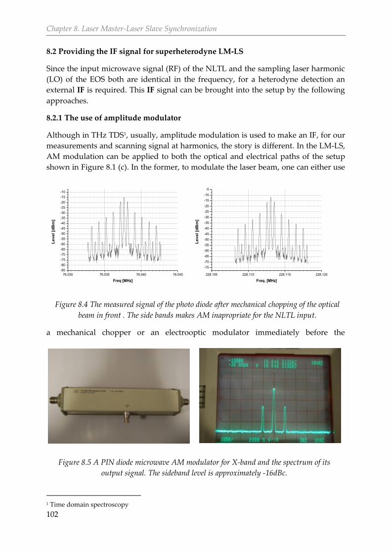
Chapter 8. Laser Master-Laser Slave Synchronization
102
8.2 Providing the IF signal for superheterodyne LM-LS
Since the input microwave signal (RF) of the NLTL and the sampling laser harmonic
(LO) of the EOS both are identical in the frequency, for a heterodyne detection an
external IF is required. This IF signal can be brought into the setup by the following
approaches.
The use of amplitude modulator 8.2.1
Although in THz TDS1, usually, amplitude modulation is used to make an IF, for our
measurements and scanning signal at harmonics, the story is different. In the LM-LS,
AM modulation can be applied to both the optical and electrical paths of the setup
shown in Figure 8.1 (c). In the former, to modulate the laser beam, one can either use
a mechanical chopper or an electrooptic modulator immediately before the
1 Time domain spectroscopy
76.030 76.035 76.040 76.045
-85
-80
-75
-70
-65
-60
-55
-50
-45
-40
-35
-30
-25
-20
-15
-10
Le
ve
l [d
Bm
]
Freq [MHz]
228.105 228.110 228.115 228.120
-75
-70
-65
-60
-55
-50
-45
-40
-35
-30
-25
-20
-15
-10
-5
Le
ve
l [d
Bm
]
Freq. [MHz]
Figure 8.4 The measured signal of the photo diode after mechanical chopping of the optical
beam in front . The side bands makes AM inapropriate for the NLTL input.
Figure 8.5 A PIN diode microwave AM modulator for X-band and the spectrum of its
output signal. The sideband level is approximately -16dBc.
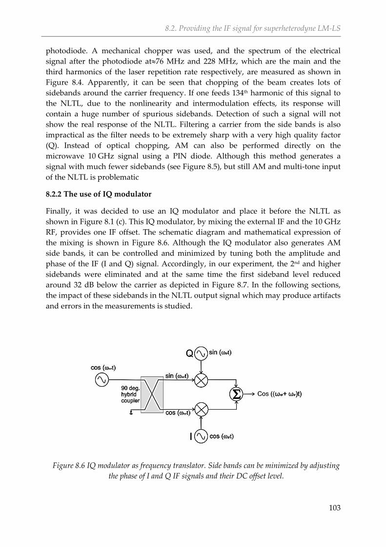
8.2. Providing the IF signal for superheterodyne LM-LS
103
photodiode. A mechanical chopper was used, and the spectrum of the electrical
signal after the photodiode at76 MHz and 228 MHz, which are the main and the
third harmonics of the laser repetition rate respectively, are measured as shown in
Figure 8.4. Apparently, it can be seen that chopping of the beam creates lots of
sidebands around the carrier frequency. If one feeds 134th harmonic of this signal to
the NLTL, due to the nonlinearity and intermodulation effects, its response will
contain a huge number of spurious sidebands. Detection of such a signal will not
show the real response of the NLTL. Filtering a carrier from the side bands is also
impractical as the filter needs to be extremely sharp with a very high quality factor
(Q). Instead of optical chopping, AM can also be performed directly on the
microwave 10 GHz signal using a PIN diode. Although this method generates a
signal with much fewer sidebands (see Figure 8.5), but still AM and multi-tone input
of the NLTL is problematic. [194]
The use of IQ modulator 8.2.2
Finally, it was decided to use an IQ modulator and place it before the NLTL as
shown in Figure 8.1 (c). This IQ modulator, by mixing the external IF and the 10 GHz
RF, provides one IF offset. The schematic diagram and mathematical expression of
the mixing is shown in Figure 8.6. Although the IQ modulator also generates AM
side bands, it can be controlled and minimized by tuning both the amplitude and
phase of the IF (I and Q) signal. Accordingly, in our experiment, the 2nd and higher
sidebands were eliminated and at the same time the first sideband level reduced
around 32 dB below the carrier as depicted in Figure 8.7. In the following sections,
the impact of these sidebands in the NLTL output signal which may produce artifacts
and errors in the measurements is studied.
Figure 8.6 IQ modulator as frequency translator. Side bands can be minimized by adjusting
the phase of I and Q IF signals and their DC offset level.
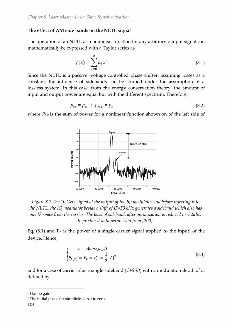
Chapter 8. Laser Master-Laser Slave Synchronization
104
The effect of AM side bands on the NLTL signal
The operation of an NLTL as a nonlinear function for any arbitrary input signal can
mathematically be expressed with a Taylor series as
( ) ∑
(8.1)
Since the NLTL is a passive1 voltage controlled phase shifter, assuming losses as a
constant, the influence of sidebands can be studied under the assumption of a
lossless system. In this case, from the energy conservation theory, the amount of
input and output power are equal but with the different spectrum. Therefore,
( )out in f xp p p p x (8.2)
where Pf(x) is the sum of power for a nonlinear function shown on of the left side of
Eq. (8.1) and PX is the power of a single carrier signal applied to the input2 of the
device. Hence,
( )
( )
| |
(8.3)
and for a case of carrier plus a single sideband (C+SSB) with a modulation depth of m
defined by
1 Has no gain 2 The initial phase for simplicity is set to zero.
Figure 8.7 The 10 GHz signal at the output of the IQ modulator and before injecting into
the NLTL. the IQ modulator beside a shift of IF=50 kHz generates a sideband which also has
one IF space from the carrier. The level of sideband, after optimization is reduced to -32dBc.
Reproduced with permission from [200].
8.2. Providing the IF signal for superheterodyne LM-LS
105
( )⏟
[( ) ]⏟
(8.4)
while x and Δx are the carrier and sideband respectively, the input power spectrum
is superimposed as
| |
| | (8.5)
Provided that the modulation index ‖
‖
and from Eq. (8.1) and Eq. (8.4), the
NLTL output for C+SSB can be approximated by
( ) ∑ ( )
∑ (
)
∑ (
)
∑ ∑
( ) ∑
⏟ ( )
(8.6)
as ( )f x reflects the only harmonics of the carrier with a spectrum at (ωc, 2ωc, 3ωc, …),
where
( ) [( ) ]∑ [ ( )]
(8.7)
represents the impact of sidebands. The spectrum of ( )f x contains (ωc± ωm, 2ωc±ωm,
3ωc±ωm,…) frequencies, which means that only the first sideband of each carrier
(harmonic) needs to be taken into account and the rest are almost suppressed. In
terms of the output power spectrum from Eq. (8.6),
( ) ( ) ( ) (8.8)
and with substituting Eq. (8.2),
( ) (8.9)
and from Eq. (8.2), Eq. (8.3) and Eq. (8.5) it follows:
( )
| |
(8.10)
These results demonstrate that for a significantly small modulation index of m, the
power of all the sidebands at the output of the NLTL equals the input sideband
power and whenever the power of the sidebands in comparison to the carrier are
small, the effect of sidebands at the NLTL output is negligible.
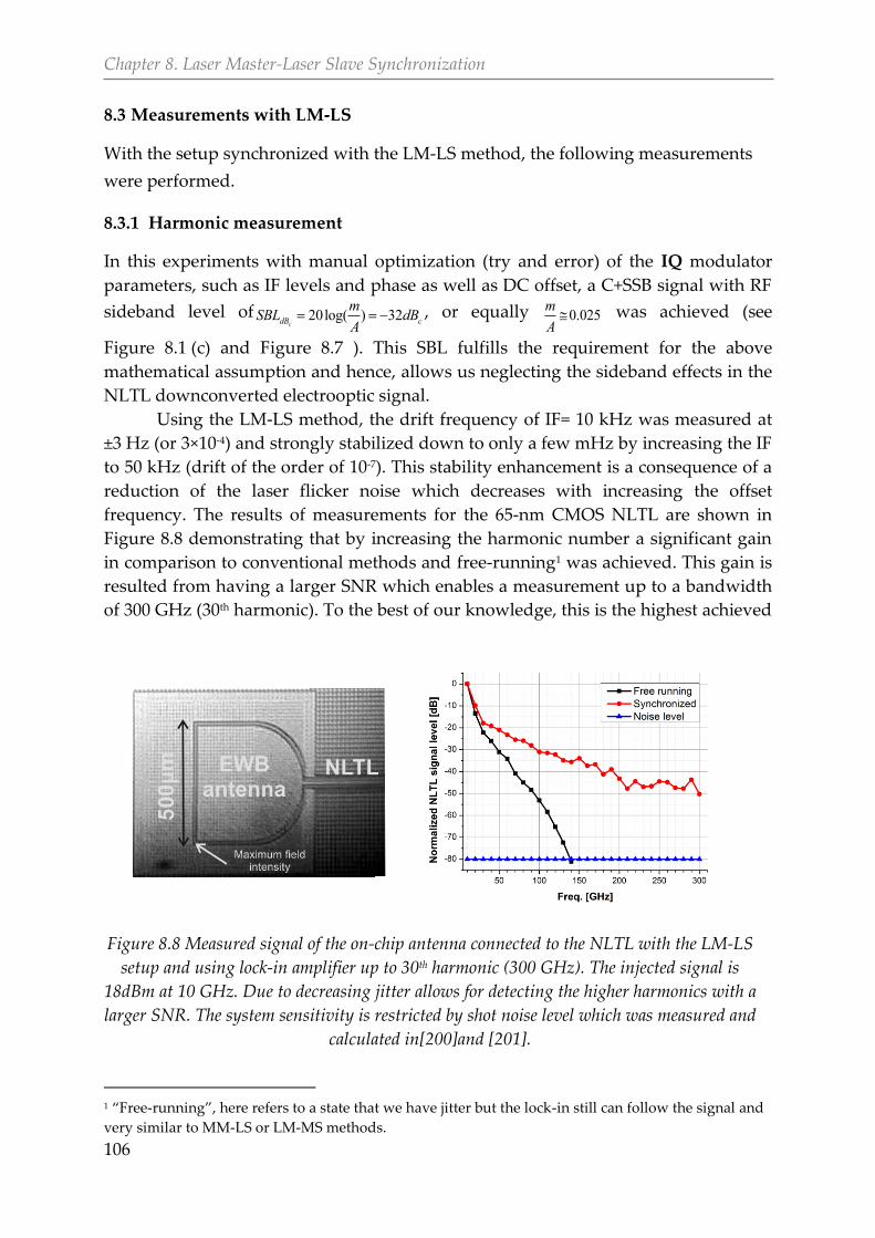
Chapter 8. Laser Master-Laser Slave Synchronization
106
8.3 Measurements with LM-LS
With the setup synchronized with the LM-LS method, the following measurements
were performed.
Harmonic measurement 8.3.1
In this experiments with manual optimization (try and error) of the IQ modulator
parameters, such as IF levels and phase as well as DC offset, a C+SSB signal with RF
sideband level of 20log( ) 32cdB c
mSBL dB
A , or equally 0.025
m
A was achieved (see
Figure 8.1 (c) and Figure 8.7 ). This SBL fulfills the requirement for the above
mathematical assumption and hence, allows us neglecting the sideband effects in the
NLTL downconverted electrooptic signal.
Using the LM-LS method, the drift frequency of IF= 10 kHz was measured at
±3 Hz (or 3×10⁻⁴) and strongly stabilized down to only a few mHz by increasing the IF
to 50 kHz (drift of the order of 10-7). This stability enhancement is a consequence of a
reduction of the laser flicker noise which decreases with increasing the offset
frequency. The results of measurements for the 65-nm CMOS NLTL are shown in
Figure 8.8 demonstrating that by increasing the harmonic number a significant gain
in comparison to conventional methods and free-running1 was achieved. This gain is
resulted from having a larger SNR which enables a measurement up to a bandwidth
of 300 GHz (30th harmonic). To the best of our knowledge, this is the highest achieved
1 “Free-running”, here refers to a state that we have jitter but the lock-in still can follow the signal and
very similar to MM-LS or LM-MS methods.
Figure 8.8 Measured signal of the on-chip antenna connected to the NLTL with the LM-LS
setup and using lock-in amplifier up to 30th harmonic (300 GHz). The injected signal is
18dBm at 10 GHz. Due to decreasing jitter allows for detecting the higher harmonics with a
larger SNR. The system sensitivity is restricted by shot noise level which was measured and
calculated in[200]and [201].
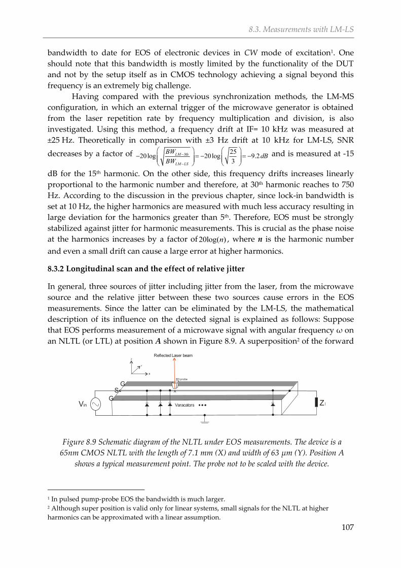
8.3. Measurements with LM-LS
107
bandwidth to date for EOS of electronic devices in CW mode of excitation1. One
should note that this bandwidth is mostly limited by the functionality of the DUT
and not by the setup itself as in CMOS technology achieving a signal beyond this
frequency is an extremely big challenge.
Having compared with the previous synchronization methods, the LM-MS
configuration, in which an external trigger of the microwave generator is obtained
from the laser repetition rate by frequency multiplication and division, is also
investigated. Using this method, a frequency drift at IF= 10 kHz was measured at
±25 Hz. Theoretically in comparison with ±3 Hz drift at 10 kHz for LM-LS, SNR
decreases by a factor of 2520log 20log 9.2
3
LM Ms
LM LS
BWdB
BW
and is measured at -15
dB for the 15th harmonic. On the other side, this frequency drifts increases linearly
proportional to the harmonic number and therefore, at 30th harmonic reaches to 750
Hz. According to the discussion in the previous chapter, since lock-in bandwidth is
set at 10 Hz, the higher harmonics are measured with much less accuracy resulting in
large deviation for the harmonics greater than 5th. Therefore, EOS must be strongly
stabilized against jitter for harmonic measurements. This is crucial as the phase noise
at the harmonics increases by a factor of 20log( )n , where n is the harmonic number
and even a small drift can cause a large error at higher harmonics.
Longitudinal scan and the effect of relative jitter 8.3.2
In general, three sources of jitter including jitter from the laser, from the microwave
source and the relative jitter between these two sources cause errors in the EOS
measurements. Since the latter can be eliminated by the LM-LS, the mathematical
description of its influence on the detected signal is explained as follows: Suppose
that EOS performs measurement of a microwave signal with angular frequency ω on
an NLTL (or LTL) at position A shown in Figure 8.9. A superposition2 of the forward
1 In pulsed pump-probe EOS the bandwidth is much larger. 2 Although super position is valid only for linear systems, small signals for the NLTL at higher
harmonics can be approximated with a linear assumption.
Z LVin
G
G
S
Reflected Laser beam
EO probe
x
Y
Z
Varacators
A
Figure 8.9 Schematic diagram of the NLTL under EOS measurements. The device is a
65nm CMOS NLTL with the length of 7.1 mm (X) and width of 63 μm (Y). Position A
shows a typical measurement point. The probe not to be scaled with the device.
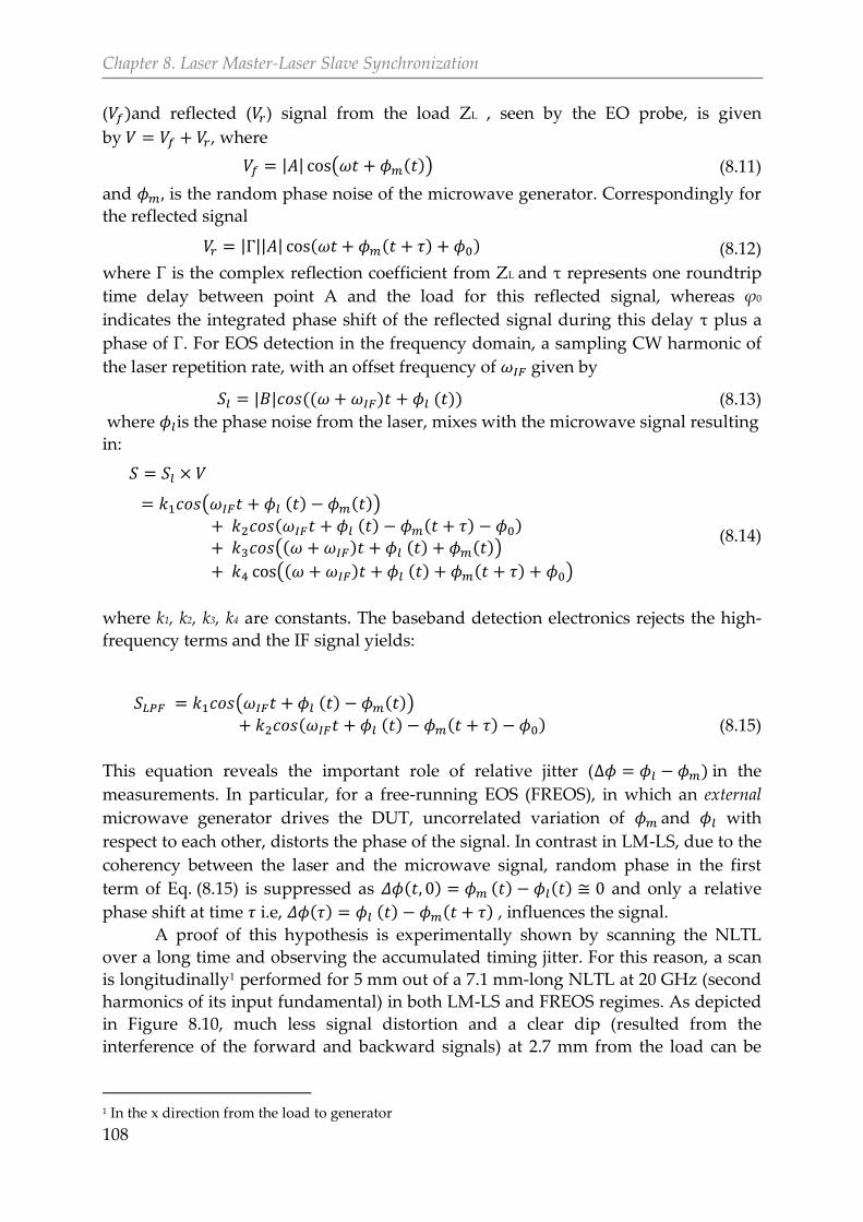
Chapter 8. Laser Master-Laser Slave Synchronization
108
( )and reflected ( ) signal from the load ZL , seen by the EO probe, is given
by , where
| | ( ( )) (8.11)
and is the random phase noise of the microwave generator. Correspondingly for
the reflected signal
| || | ( ( ) ) (8.12)
where Γ is the complex reflection coefficient from ZL and τ represents one roundtrip
time delay between point A and the load for this reflected signal, whereas ϕ0
indicates the integrated phase shift of the reflected signal during this delay τ plus a
phase of Γ. For EOS detection in the frequency domain, a sampling CW harmonic of
the laser repetition rate, with an offset frequency of given by
| | (( ) ( )) (8.13)
where is the phase noise from the laser, mixes with the microwave signal resulting
in:
( ( ) ( ))
( ( ) ( ) )
(( ) ( ) ( ))
(( ) ( ) ( ) )
(8.14)
where k1, k2, k3, k4 are constants. The baseband detection electronics rejects the high-
frequency terms and the IF signal yields:
( ( ) ( ))
( ( ) ( ) )
(8.15)
This equation reveals the important role of relative jitter ( ) in the
measurements. In particular, for a free-running EOS (FREOS), in which an external
microwave generator drives the DUT, uncorrelated variation of and with
respect to each other, distorts the phase of the signal. In contrast in LM-LS, due to the
coherency between the laser and the microwave signal, random phase in the first
term of Eq. (8.15) is suppressed as ( ) ( ) ( ) and only a relative
phase shift at time i.e, ( ) ( ) ( ) , influences the signal.
A proof of this hypothesis is experimentally shown by scanning the NLTL
over a long time and observing the accumulated timing jitter. For this reason, a scan
is longitudinally1 performed for 5 mm out of a 7.1 mm-long NLTL at 20 GHz (second
harmonics of its input fundamental) in both LM-LS and FREOS regimes. As depicted
in Figure 8.10, much less signal distortion and a clear dip (resulted from the
interference of the forward and backward signals) at 2.7 mm from the load can be
1 In the x direction from the load to generator
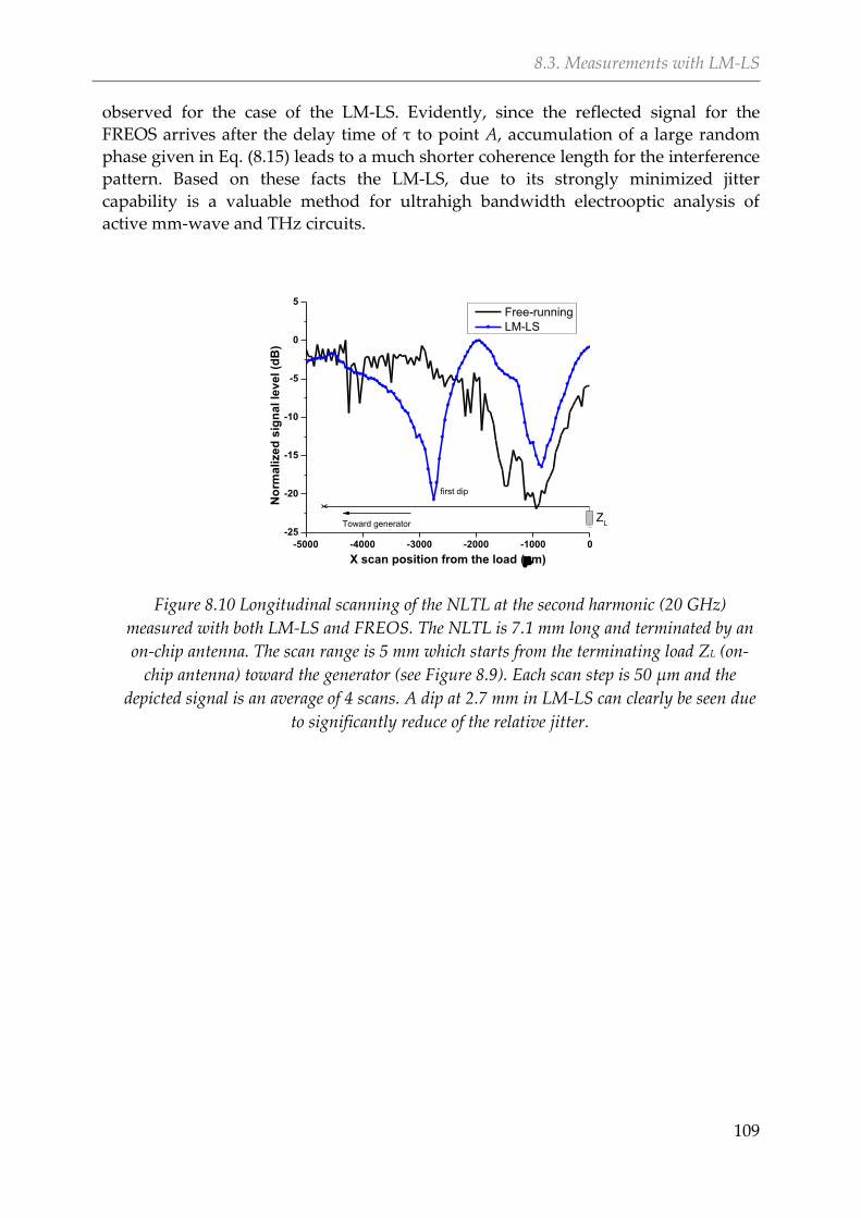
8.3. Measurements with LM-LS
109
observed for the case of the LM-LS. Evidently, since the reflected signal for the
FREOS arrives after the delay time of τ to point A, accumulation of a large random
phase given in Eq. (8.15) leads to a much shorter coherence length for the interference
pattern. Based on these facts the LM-LS, due to its strongly minimized jitter
capability is a valuable method for ultrahigh bandwidth electrooptic analysis of
active mm-wave and THz circuits.
-5000 -4000 -3000 -2000 -1000 0
-25
-20
-15
-10
-5
0
5
No
rma
lize
d s
ign
al le
ve
l (d
B)
X scan position from the load (m)
Free-running
LM-LS
first dip
Toward generatorZ
L
Figure 8.10 Longitudinal scanning of the NLTL at the second harmonic (20 GHz)
measured with both LM-LS and FREOS. The NLTL is 7.1 mm long and terminated by an
on-chip antenna. The scan range is 5 mm which starts from the terminating load ZL (on-
chip antenna) toward the generator (see Figure 8.9). Each scan step is 50 μm and the
depicted signal is an average of 4 scans. A dip at 2.7 mm in LM-LS can clearly be seen due
to significantly reduce of the relative jitter.

111
Optical Network Analysis 9.
Measurements
In Chapter 3, recent advances in electronic network analyzer extension modules for
the characterization of ultrafast electronic devices up to 1.1 THz were explained. It
was also mentioned about the drawbacks of this approach such challenging
calibration [83], and alternatively, EOS was introduced. At this time, it is good to
stress on the use of this approach for mm-wave network analysis. Although, some
work such as [130], [154], [195]–[197] have demonstrated EOS for S-parameter
measurements of transmission lines and passive structures, only few attention [133]
have been paid to nonlinear and active devices. In this chapter, NLTL measurements
and capabilities of EOS in measuring S-parameters, standing waves, effective
permittivity, as well as dispersion are demonstrated.
It is necessary to mention that in contrast to works such as [97] and [140],
instead of using a photoconductive pulse, here, the CW excitation of the devices is
used for the characterization of active or nonlinear devices.. Because, the response of
a nonlinear system to a short pulse and hence, using convolution, will not lead us to
a meaningful interpretation of the system behavior. Also, the response of a nonlinear
system strongly depends on the level of the applied signal to DUT and working in
small or large signal regimes must be considered. This concept is also valid for
electronic network analyzers as recently the large signal measurements in nonlinear
systems have been presented with X-parameters instead of S-parameters [198]. The
good thing is that in our EOS measurements at the signal harmonics can be
performed by filtering each harmonic with a lock-in amplifier or the Fourier
transformation without concerning about the complex mathematical analysis of the
nonlinear system.
9.1 Device under test
Two NLTLs including a single-port device with on-chip 50 Ω load terminated, and a
two-port device so called quasi-open, were subjected to the measurements (see
Figure 9.1). Both these lines, excluding their bonding pads have a length of 7.1 mm
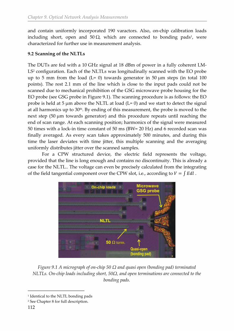
Chapter 9. Optical Network Analysis Measurements
112
and contain uniformly incorporated 190 varactors. Also, on-chip calibration loads
including short, open and 50 Ω, which are connected to bonding pads1, were
characterized for further use in measurement analysis.
9.2 Scanning of the NLTLs
The DUTs are fed with a 10 GHz signal at 18 dBm of power in a fully coherent LM-
LS2 configuration. Each of the NLTLs was longitudinally scanned with the EO probe
up to 5 mm from the load (L= 0) towards generator in 50 μm steps (in total 100
points). The rest 2.1 mm of the line which is close to the input pads could not be
scanned due to mechanical prohibition of the GSG microwave probe housing for the
EO probe (see GSG probe in Figure 9.1). The scanning procedure is as follows: the EO
probe is held at 5 μm above the NLTL at load (L= 0) and we start to detect the signal
at all harmonics up to 30th. By ending of this measurement, the probe is moved to the
next step (50 μm towards generator) and this procedure repeats until reaching the
end of scan range. At each scanning position; harmonics of the signal were measured
50 times with a lock-in time constant of 50 ms (BW= 20 Hz) and 6 recorded scan was
finally averaged. As every scan takes approximately 500 minutes, and during this
time the laser deviates with time jitter, this multiple scanning and the averaging
uniformly distributes jitter over the scanned samples.
For a CPW structured device, the electric field represents the voltage,
provided that the line is long enough and contains no discontinuity. This is already a
case for the NLTL.. The voltage can even be precisely calculated from the integrating
of the field tangential component over the CPW slot, i.e., according to ∫ .
1 Identical to the NLTL bonding pads 2 See Chapter 8 for full description.
Figure 9.1 A micrograph of on-chip 50 Ω and quasi open (bonding pad) terminated
NLTLs. On-chip loads including short, 50Ω, and open terminations are connected to the
bonding pads.
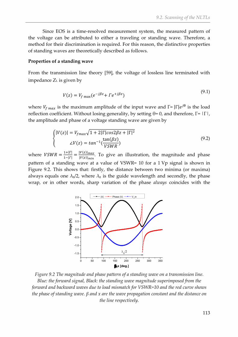
9.2. Scanning of the NLTLs
113
Since EOS is a time-resolved measurement system, the measured pattern of
the voltage can be attributed to either a traveling or standing wave. Therefore, a
method for their discrimination is required. For this reason, the distinctive properties
of standing waves are theoretically described as follows.
Properties of a standing wave
From the transmission line theory [59], the voltage of lossless line terminated with
impedance ZL is given by
( ) (
) (9.1)
where is the maximum amplitude of the input wave and Γ= | | is the load
reflection coefficient. Without losing generality, by setting θ= 0, and therefore, Γ= |Γ|,
the amplitude and phase of a voltage standing wave are given by
| ( )| √ | | | |
( ) ( ( )
)
(9.2)
where | |
| |
| ( )|
| ( )| . To give an illustration, the magnitude and phase
pattern of a standing wave at a value of VSWR= 10 for a 1 Vp signal is shown in
Figure 9.2. This shows that: firstly, the distance between two minima (or maxima)
always equals one λg/2, where λg is the guide wavelength and secondly, the phase
wrap, or in other words, sharp variation of the phase always coincides with the
0 50 100 150 200 250 300 350
-1.5
-1.0
-0.5
0.0
0.5
1.0
1.5
2.0
x [deg.]
|V| Phase (V) V_in
g
Vo
lta
ge
[V
]
Figure 9.2 The magnitude and phase pattern of a standing wave on a transmission line.
Blue: the forward signal, Black: the standing wave magnitude superimposed from the
forward and backward waves due to load mismatch for VSWR=10 and the red curve shows
the phase of standing wave. β and x are the wave propagation constant and the distance on
the line respectively.
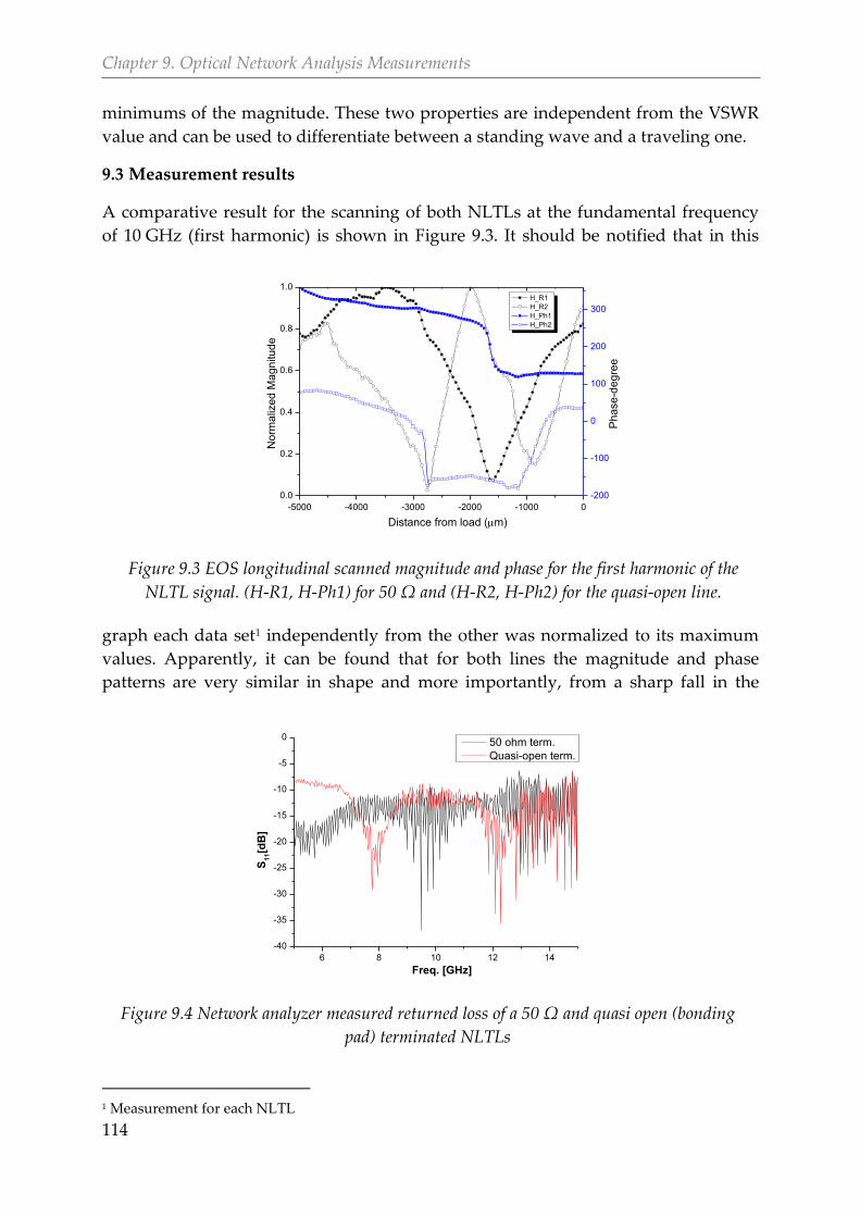
Chapter 9. Optical Network Analysis Measurements
114
minimums of the magnitude. These two properties are independent from the VSWR
value and can be used to differentiate between a standing wave and a traveling one.
9.3 Measurement results
A comparative result for the scanning of both NLTLs at the fundamental frequency
of 10 GHz (first harmonic) is shown in Figure 9.3. It should be notified that in this
graph each data set1 independently from the other was normalized to its maximum
values. Apparently, it can be found that for both lines the magnitude and phase
patterns are very similar in shape and more importantly, from a sharp fall in the
1 Measurement for each NLTL
6 8 10 12 14
-40
-35
-30
-25
-20
-15
-10
-5
0
S1
1[d
B]
Freq. [GHz]
50 ohm term.
Quasi-open term.
Figure 9.4 Network analyzer measured returned loss of a 50 Ω and quasi open (bonding
pad) terminated NLTLs
-5000 -4000 -3000 -2000 -1000 0
0.0
0.2
0.4
0.6
0.8
1.0 H_R1
H_R2
H_Ph1
H_Ph2
Distance from load (m)
No
rma
lize
d M
ag
nitu
de
-200
-100
0
100
200
300
Ph
ase
-de
gre
e
Figure 9.3 EOS longitudinal scanned magnitude and phase for the first harmonic of the
NLTL signal. (H-R1, H-Ph1) for 50 Ω and (H-R2, H-Ph2) for the quasi-open line.
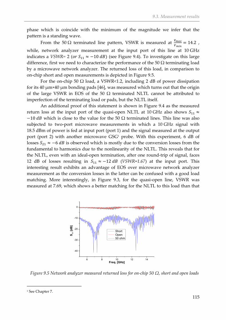
9.3. Measurement results
115
phase which is coincide with the minimum of the magnitude we infer that the
pattern is a standing wave.
From the 50 Ω terminated line pattern, VSWR is measured at
,
while, network analyzer measurement at the input port of this line at 10 GHz
indicates a VSWR= 2 ( ) (see Figure 9.4). To investigate on this large
difference, first we need to characterize the performance of the 50 Ω terminating load
by a microwave network analyzer. The returned loss of this load, in comparison to
on-chip short and open measurements is depicted in Figure 9.5.
For the on-chip 50 Ω load, a VSWR<1.2, including 2 dB of power dissipation
for its 40 μm×40 μm bonding pads [46], was measured which turns out that the origin
of the large VSWR in EOS of the 50 Ω terminated NLTL cannot be attributed to
imperfection of the terminating load or pads, but the NLTL itself.
An additional proof of this statement is shown in Figure 9.4 as the measured
return loss at the input port of the quasi-open NLTL at 10 GHz also shows
which is close to the value for the 50 Ω terminated lines. This line was also
subjected to two-port microwave measurements in which a 10 GHz signal with
18.5 dBm of power is fed at input port (port 1) and the signal measured at the output
port (port 2) with another microwave GSG1 probe. With this experiment, 6 dB of
losses is observed which is mostly due to the conversion losses from the
fundamental to harmonics due to the nonlinearity of the NLTL. This reveals that for
the NLTL, even with an ideal-open termination, after one round-trip of signal, faces
12 dB of losses resulting in (VSWR=1.67) at the input port. This
interesting result exhibits an advantage of EOS over microwave network analyzer
measurement as the conversion losses in the latter can be confused with a good load
matching. More interestingly, in Figure 9.3, for the quasi-open line, VSWR was
measured at 7.69, which shows a better matching for the NLTL to this load than that
1 See Chapter 7.
6 8 10 12 14
-40
-30
-20
-10
0
S1
1 [
dB
]
Freq. [GHz]
Short
Open
50 ohm
Figure 9.5 Network analyzer measured returned loss for on-chip 50 Ω, short and open loads
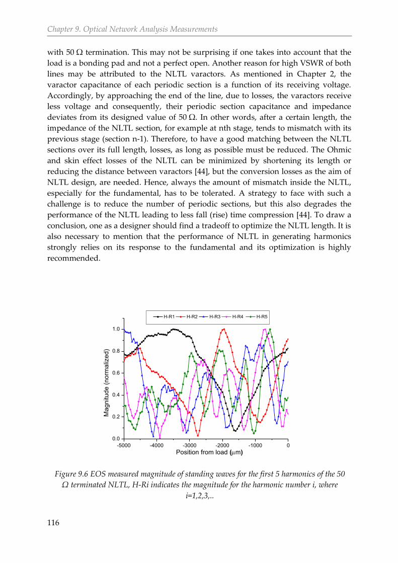
Chapter 9. Optical Network Analysis Measurements
116
with 50 Ω termination. This may not be surprising if one takes into account that the
load is a bonding pad and not a perfect open. Another reason for high VSWR of both
lines may be attributed to the NLTL varactors. As mentioned in Chapter 2, the
varactor capacitance of each periodic section is a function of its receiving voltage.
Accordingly, by approaching the end of the line, due to losses, the varactors receive
less voltage and consequently, their periodic section capacitance and impedance
deviates from its designed value of 50 Ω. In other words, after a certain length, the
impedance of the NLTL section, for example at nth stage, tends to mismatch with its
previous stage (section n-1). Therefore, to have a good matching between the NLTL
sections over its full length, losses, as long as possible must be reduced. The Ohmic
and skin effect losses of the NLTL can be minimized by shortening its length or
reducing the distance between varactors [44], but the conversion losses as the aim of
NLTL design, are needed. Hence, always the amount of mismatch inside the NLTL,
especially for the fundamental, has to be tolerated. A strategy to face with such a
challenge is to reduce the number of periodic sections, but this also degrades the
performance of the NLTL leading to less fall (rise) time compression [44]. To draw a
conclusion, one as a designer should find a tradeoff to optimize the NLTL length. It is
also necessary to mention that the performance of NLTL in generating harmonics
strongly relies on its response to the fundamental and its optimization is highly
recommended.
-5000 -4000 -3000 -2000 -1000 0
0.0
0.2
0.4
0.6
0.8
1.0
Ma
gn
itu
de
(n
orm
aliz
ed
)
Position from load (m)
H-R1 H-R2 H-R3 H-R4 H-R5
Figure 9.6 EOS measured magnitude of standing waves for the first 5 harmonics of the 50
Ω terminated NLTL, H-Ri indicates the magnitude for the harmonic number i, where
i=1,2,3,..
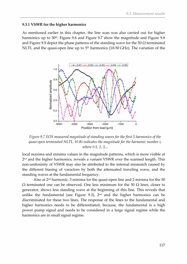
9.3. Measurement results
117
VSWR for the higher harmonics 9.3.1
As mentioned earlier in this chapter, the line scan was also carried out for higher
harmonics up to 30th. Figure 9.6 and Figure 9.7 show the magnitude and Figure 9.8
and Figure 9.9 depict the phase patterns of the standing wave for the 50 Ω terminated
NLTL and the quasi-open line up to 5th harmonics (10-50 GHz). The variation of the
local maxima and minima values in the magnitude patterns, which is more visible at
2nd and the higher harmonics, reveals a variant VSWR over the scanned length. This
non-uniformity of VSWR may also be attributed to the internal mismatch caused by
the different biasing of varactors by both the attenuated traveling wave, and the
standing waves at the fundamental frequency.
Also at 2nd harmonic, 3 minima for the quasi-open line and 2 minima for the 50
Ω terminated one can be observed. One less minimum for the 50 Ω lines, closer to
generator, shows less standing wave at the beginning of this line. This reveals that
unlike the fundamental (see Figure 9.3), 2nd and the higher harmonics can be
discriminated for these two lines. The response of the lines to the fundamental and
higher harmonics needs to be differentiated, because, the fundamental is a high
power pump signal and needs to be considered in a large signal regime while the
harmonics are in small signal regime.
-5000 -4000 -3000 -2000 -1000 0
0.0
0.2
0.4
0.6
0.8
1.0
No
rma
lize
d a
mp
litu
de
Position from load (m)
H-R1 H-R2 H-R3 H-R4 H-R5
Figure 9.7 EOS measured magnitude of standing waves for the first 5 harmonics of the
quasi-open terminated NLTL. H-Ri indicates the magnitude for the harmonic number i,
where i=1, 2, 3,..
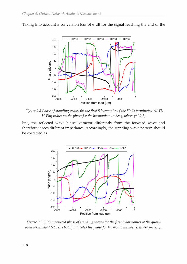
Chapter 9. Optical Network Analysis Measurements
118
Taking into account a conversion loss of 6 dB for the signal reaching the end of the
line, the reflected wave biases varactor differently from the forward wave and
therefore it sees different impedance. Accordingly, the standing wave pattern should
be corrected as
-5000 -4000 -3000 -2000 -1000 0
-200
-150
-100
-50
0
50
100
150
200
Ph
ase
(d
eg
ree
)
Position from load (m)
H-Phi1 H-Phi2 H-Phi3 H-Phi4 H-Phi5
Figure 9.8 Phase of standing waves for the first 5 harmonics of the 50 Ω terminated NLTL.
H-Phij indicates the phase for the harmonic number j, where j=1,2,3,..
-5000 -4000 -3000 -2000 -1000 0
-200
-150
-100
-50
0
50
100
150
200
Ph
ase
(d
eg
ree
)
Position from load (m)
H-Phi1 H-Phi2 H-Phi3 H-Phi4 H-Phi5
Figure 9.9 EOS measured phase of standing waves for the first 5 harmonics of the quasi-
open terminated NLTL. H-Phij indicates the phase for harmonic number j, where j=1,2,3,..
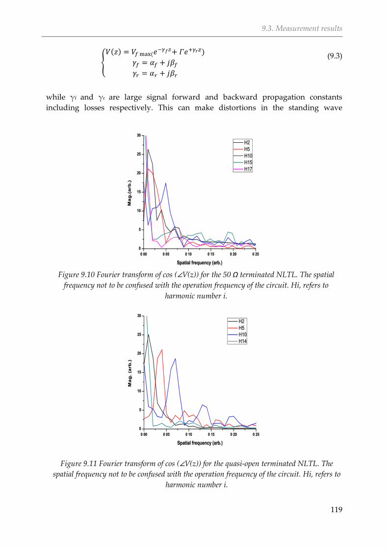
9.3. Measurement results
119
( ) (
)
(9.3)
while γf and γr are large signal forward and backward propagation constants
including losses respectively. This can make distortions in the standing wave
Figure 9.11 Fourier transform of cos ( V(z)) for the quasi-open terminated NLTL. The
spatial frequency not to be confused with the operation frequency of the circuit. Hi, refers to
harmonic number i.
Figure 9.10 Fourier transform of cos ( V(z)) for the 50 Ω terminated NLTL. The spatial
frequency not to be confused with the operation frequency of the circuit. Hi, refers to
harmonic number i.
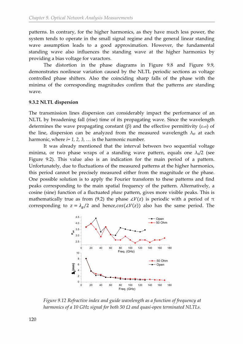
Chapter 9. Optical Network Analysis Measurements
120
patterns. In contrary, for the higher harmonics, as they have much less power, the
system tends to operate in the small signal regime and the general linear standing
wave assumption leads to a good approximation. However, the fundamental
standing wave also influences the standing wave at the higher harmonics by
providing a bias voltage for varactors.
The distortion in the phase diagrams in Figure 9.8 and Figure 9.9,
demonstrates nonlinear variation caused by the NLTL periodic sections as voltage
controlled phase shifters. Also the coinciding sharp falls of the phase with the
minima of the corresponding magnitudes confirm that the patterns are standing
wave.
NLTL dispersion 9.3.2
The transmission lines dispersion can considerably impact the performance of an
NLTL by broadening fall (rise) time of its propagating wave. Since the wavelength
determines the wave propagating constant (β) and the effective permittivity (εeff) of
the line, dispersion can be analyzed from the measured wavelength λgi at each
harmonic, where i= 1, 2, 3, … is the harmonic number.
It was already mentioned that the interval between two sequential voltage
minima, or two phase wraps of a standing wave pattern, equals one λg/2 (see
Figure 9.2). This value also is an indication for the main period of a pattern.
Unfortunately, due to fluctuations of the measured patterns at the higher harmonics,
this period cannot be precisely measured either from the magnitude or the phase.
One possible solution is to apply the Fourier transform to these patterns and find
peaks corresponding to the main spatial frequency of the pattern. Alternatively, a
cosine (sine) function of a fluctuated phase pattern, gives more visible peaks. This is
mathematically true as from (9.2) the phase ( ) is periodic with a period of π
corresponding to and hence, ( ( )) also has the same period. The
0 20 40 60 80 100 120 140 160 180
0
2
4
6
8
10
50 Ohm
Open
g(m
m)
Freq. (GHz)
0 20 40 60 80 100 120 140 160 180
2.5
3.0
3.5
4.0
4.5 Open
50 Ohm
ne
ff
Freq. (GHz)
Figure 9.12 Refractive index and guide wavelength as a function of frequency at
harmonics of a 10 GHz signal for both 50 Ω and quasi-open terminated NLTLs.
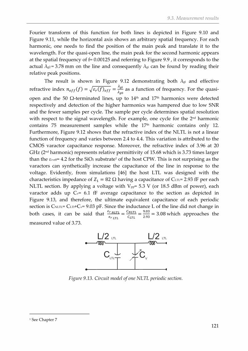
9.3. Measurement results
121
Fourier transform of this function for both lines is depicted in Figure 9.10 and
Figure 9.11, while the horizontal axis shows an arbitrary spatial frequency. For each
harmonic, one needs to find the position of the main peak and translate it to the
wavelength. For the quasi-open line, the main peak for the second harmonic appears
at the spatial frequency of f= 0.00125 and referring to Figure 9.9 , it corresponds to the
actual λg2 = 3.78 mm on the line and consequently λgi can be found by reading their
relative peak positions.
The result is shown in Figure 9.12 demonstrating both λgi and effective
refractive index ( ) √ ( )
as a function of frequency. For the quasi-
open and the 50 Ω-terminated lines, up to 14th and 17th harmonics were detected
respectively and detection of the higher harmonics was hampered due to low SNR
and the fewer samples per cycle. The sample per cycle determines spatial resolution
with respect to the signal wavelength. For example, one cycle for the 2nd harmonic
contains 75 measurement samples while the 17th harmonic contains only 12.
Furthermore, Figure 9.12 shows that the refractive index of the NLTL is not a linear
function of frequency and varies between 2.4 to 4.4. This variation is attributed to the
CMOS varactor capacitance response. Moreover, the refractive index of 3.96 at 20
GHz (2nd harmonic) represents relative permittivity of 15.68 which is 3.73 times larger
than the εr-eff= 4.2 for the SiO2 substrate1 of the host CPW. This is not surprising as the
varactors can synthetically increase the capacitance of the line in response to the
voltage. Evidently, from simulations [46] the host LTL was designed with the
characteristics impedance of Ω having a capacitance of CLTL= 2.93 fF per each
NLTL section. By applying a voltage with Vpp= 5.3 V (or 18.5 dBm of power), each
varactor adds up Cv= 6.1 fF average capacitance to the section as depicted in
Figure 9.13, and therefore, the ultimate equivalent capacitance of each periodic
section is CNLTL= CLTl+Cv= 9.03 pF. Since the inductance L of the line did not change in
both cases, it can be said that
which approaches the
measured value of 3.73.
1 See Chapter 7
CLTL
CV
L/2 LTL L/2 LTL
Figure 9.13. Circuit model of one NLTL periodic section.

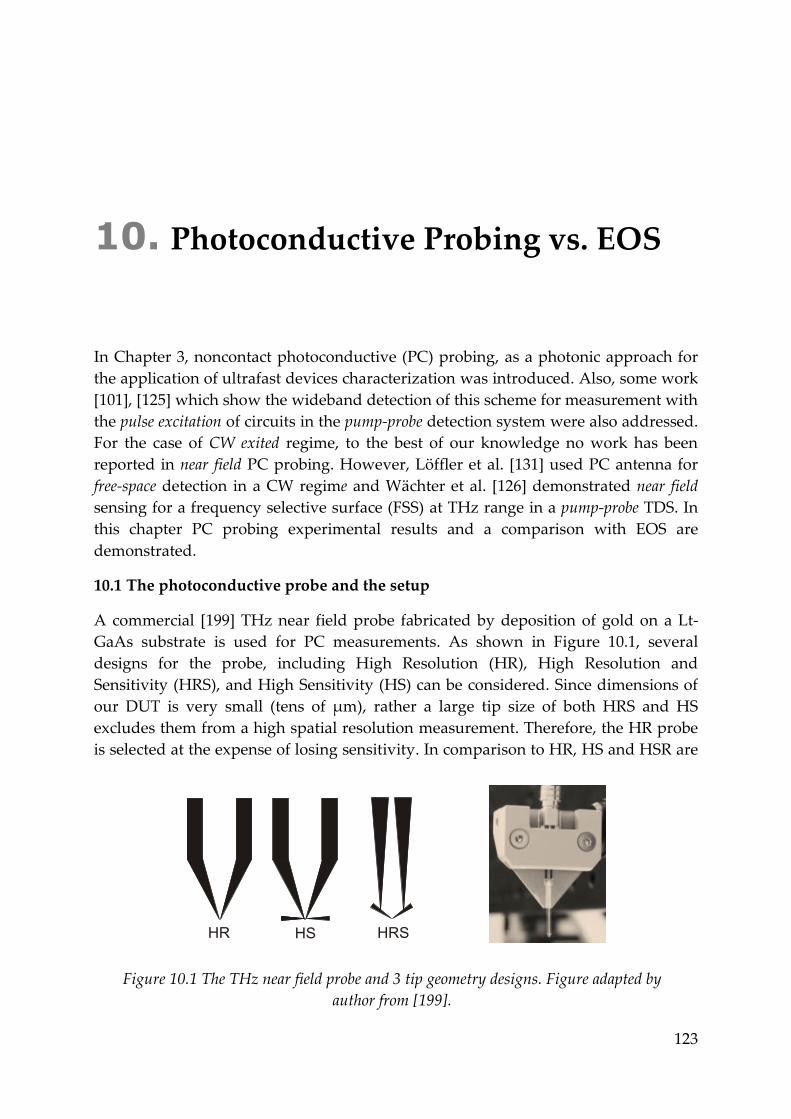
123
Photoconductive Probing vs. EOS 10.
In Chapter 3, noncontact photoconductive (PC) probing, as a photonic approach for
the application of ultrafast devices characterization was introduced. Also, some work
[101], [125] which show the wideband detection of this scheme for measurement with
the pulse excitation of circuits in the pump-probe detection system were also addressed.
For the case of CW exited regime, to the best of our knowledge no work has been
reported in near field PC probing. However, Löffler et al. [131] used PC antenna for
free-space detection in a CW regime and Wächter et al. [126] demonstrated near field
sensing for a frequency selective surface (FSS) at THz range in a pump-probe TDS. In
this chapter PC probing experimental results and a comparison with EOS are
demonstrated.
10.1 The photoconductive probe and the setup
A commercial [199] THz near field probe fabricated by deposition of gold on a Lt-
GaAs substrate is used for PC measurements. As shown in Figure 10.1, several
designs for the probe, including High Resolution (HR), High Resolution and
Sensitivity (HRS), and High Sensitivity (HS) can be considered. Since dimensions of
our DUT is very small (tens of μm), rather a large tip size of both HRS and HS
excludes them from a high spatial resolution measurement. Therefore, the HR probe
is selected at the expense of losing sensitivity. In comparison to HR, HS and HSR are
HR HS HRS
Figure 10.1 The THz near field probe and 3 tip geometry designs. Figure adapted by
author from [199].
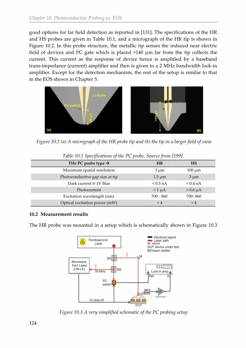
Chapter 10. Photoconductive Probing vs. EOS
124
good options for far field detection as reported in [131]. The specifications of the HR
and HS probes are given in Table 10.1, and a micrograph of the HR tip is shown in
Figure 10.2. In this probe structure, the metallic tip senses the induced near electric
field of devices and PC gate which is placed ≈140 μm far from the tip collects the
current. This current as the response of device hence is amplified by a baseband
trans-impedance (current) amplifier and then is given to a 2 MHz bandwidth lock-in
amplifier. Except for the detection mechanism, the rest of the setup is similar to that
in the EOS shown in Chapter 5.
Table 10.1 Specifications of the PC probe. Source from [199].
THz PC probe type HR HS
Maximum spatial resolution 3 µm 100 µm
Photoconductive gap size at tip 1.5 µm 3 µm
Dark current @ 1V Bias < 0.5 nA < 0.4 nA
Photocurrent > 1 µA > 0.6 µA
Excitation wavelength (nm) 700 - 860 700- 860
Optical excitation power (mW) < 4 < 4
10.2 Measurement results
The HR probe was mounted in a setup which is schematically shown in Figure 10.3
Figure 10.2 (a) A micrograph of the HR probe tip and (b) the tip in a larger field of view
DUT
M
PC probe
Femtosecond Laser
Electrical signalLaser path
M: mirrorDUT: device under testBS:beam splitter
Lock-in amp.
Ref In
PCswitch
76 MHz
10 GHz+IF
Current amp.
BS
BS
A
Figure 10.3 A very simplified schematic of the PC probing setup
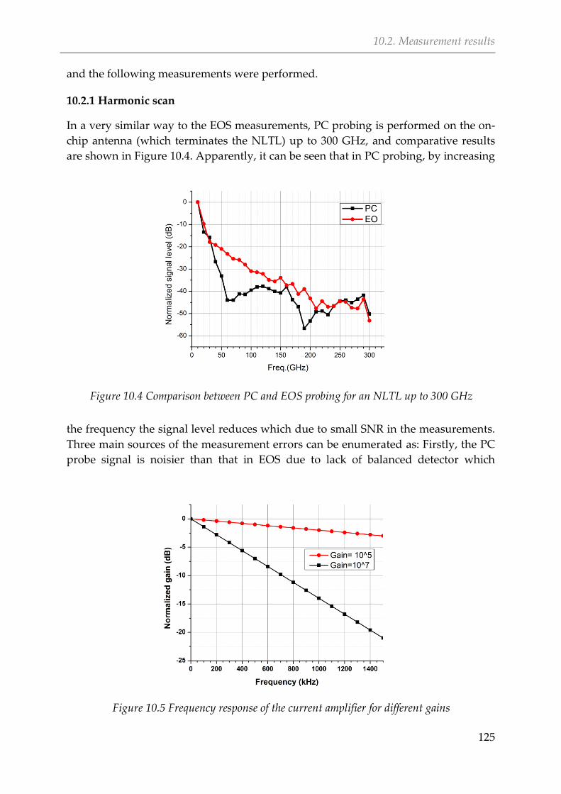
10.2. Measurement results
125
and the following measurements were performed.
Harmonic scan 10.2.1
In a very similar way to the EOS measurements, PC probing is performed on the on-
chip antenna (which terminates the NLTL) up to 300 GHz, and comparative results
are shown in Figure 10.4. Apparently, it can be seen that in PC probing, by increasing
the frequency the signal level reduces which due to small SNR in the measurements.
Three main sources of the measurement errors can be enumerated as: Firstly, the PC
probe signal is noisier than that in EOS due to lack of balanced detector which
Figure 10.4 Comparison between PC and EOS probing for an NLTL up to 300 GHz
Figure 10.5 Frequency response of the current amplifier for different gains
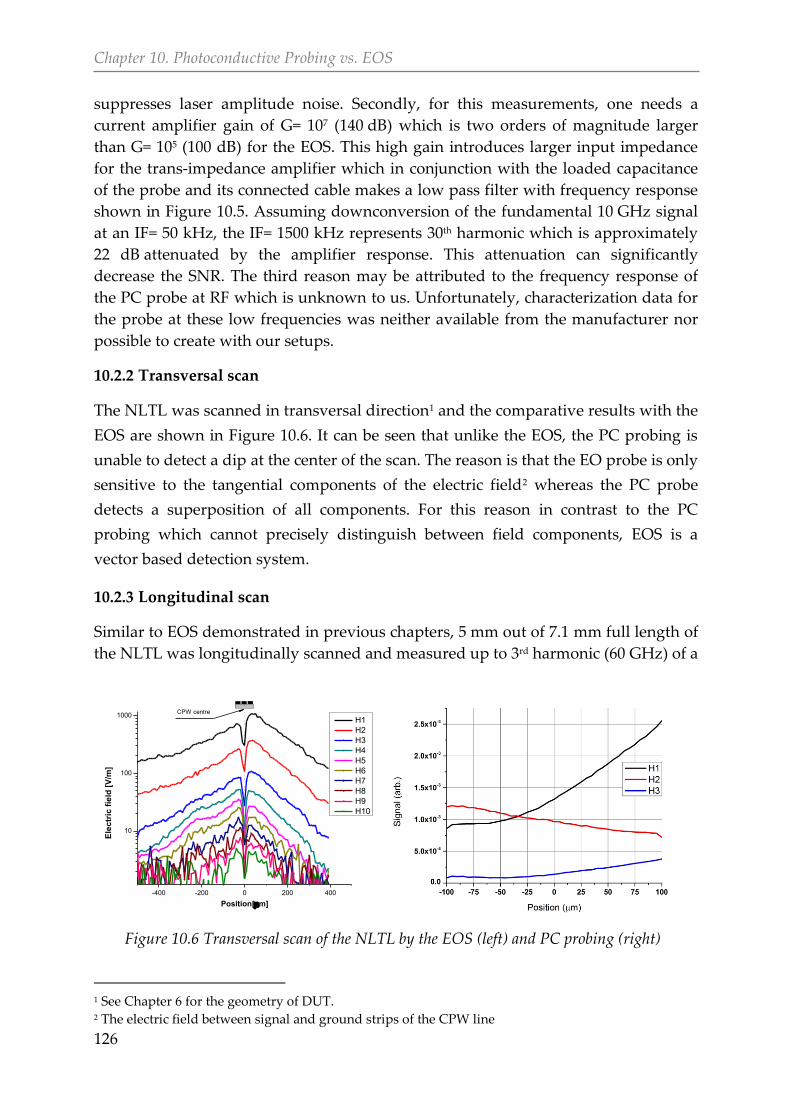
Chapter 10. Photoconductive Probing vs. EOS
126
suppresses laser amplitude noise. Secondly, for this measurements, one needs a
current amplifier gain of G= 107 (140 dB) which is two orders of magnitude larger
than G= 105 (100 dB) for the EOS. This high gain introduces larger input impedance
for the trans-impedance amplifier which in conjunction with the loaded capacitance
of the probe and its connected cable makes a low pass filter with frequency response
shown in Figure 10.5. Assuming downconversion of the fundamental 10 GHz signal
at an IF= 50 kHz, the IF= 1500 kHz represents 30th harmonic which is approximately
22 dB attenuated by the amplifier response. This attenuation can significantly
decrease the SNR. The third reason may be attributed to the frequency response of
the PC probe at RF which is unknown to us. Unfortunately, characterization data for
the probe at these low frequencies was neither available from the manufacturer nor
possible to create with our setups.
Transversal scan 10.2.2
The NLTL was scanned in transversal direction1 and the comparative results with the
EOS are shown in Figure 10.6. It can be seen that unlike the EOS, the PC probing is
unable to detect a dip at the center of the scan. The reason is that the EO probe is only
sensitive to the tangential components of the electric field2 whereas the PC probe
detects a superposition of all components. For this reason in contrast to the PC
probing which cannot precisely distinguish between field components, EOS is a
vector based detection system.
Longitudinal scan 10.2.3
Similar to EOS demonstrated in previous chapters, 5 mm out of 7.1 mm full length of
the NLTL was longitudinally scanned and measured up to 3rd harmonic (60 GHz) of a
1 See Chapter 6 for the geometry of DUT. 2 The electric field between signal and ground strips of the CPW line
-400 -200 0 200 400
10
100
1000
Ele
ctr
ic f
ield
[V
/m]
Position[m]
H1
H2
H3
H4
H5
H6
H7
H8
H9
H10
CPW centre
Figure 10.6 Transversal scan of the NLTL by the EOS (left) and PC probing (right)
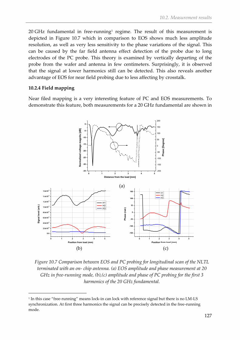
10.2. Measurement results
127
20 GHz fundamental in free-running1 regime. The result of this measurement is
depicted in Figure 10.7 which in comparison to EOS shows much less amplitude
resolution, as well as very less sensitivity to the phase variations of the signal. This
can be caused by the far field antenna effect detection of the probe due to long
electrodes of the PC probe. This theory is examined by vertically departing of the
probe from the wafer and antenna in few centimeters. Surprisingly, it is observed
that the signal at lower harmonics still can be detected. This also reveals another
advantage of EOS for near field probing due to less affecting by crosstalk.
Field mapping 10.2.4
Near filed mapping is a very interesting feature of PC and EOS measurements. To
demonstrate this feature, both measurements for a 20 GHz fundamental are shown in
1 In this case “free-running” means lock-in can lock with reference signal but there is no LM-LS
synchronization. At first three harmonics the signal can be precisely detected in the free-running
mode.
0 1 2 3 4 5
-35
-30
-25
-20
-15
-10
-5
0
No
rma
lize
d v
olt
ag
e m
ag
nit
u [
dB
]
Distance from the load [mm]
-200
-150
-100
-50
0
50
100
150
200
Ph
as
e [
De
gre
e]
0 1 2 3 4 5
-160
-106
-53
0
53
106
160
Ph
as
e (
rad
.)
Position from load (mm)
H1
H2
H3
0 1 2 3 4 5
0.0
2.0x10⁻⁴
4.0x10⁻⁴
6.0x10⁻⁴
8.0x10⁻⁴
1.0x10⁻³
1.2x10⁻³
1.4x10⁻³
1.6x10⁻³
Sig
na
l le
ve
l (a
rb.)
Position from load (mm)
H1
H2
H3
Figure 10.7 Comparison between EOS and PC probing for longitudinal scan of the NLTL
terminated with an on- chip antenna. (a) EOS amplitude and phase measurement at 20
GHz in free-running mode, (b),(c) amplitude and phase of PC probing for the first 3
harmonics of the 20 GHz fundamental.
(c) (b)
(a)
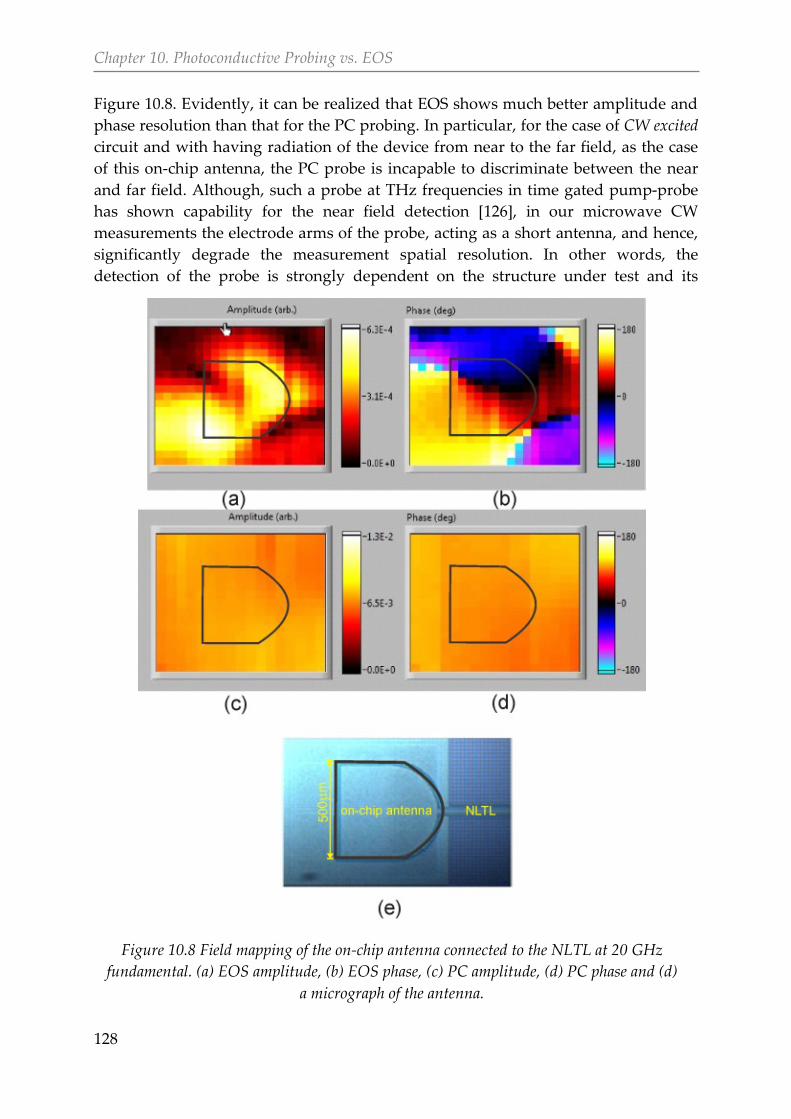
Chapter 10. Photoconductive Probing vs. EOS
128
Figure 10.8. Evidently, it can be realized that EOS shows much better amplitude and
phase resolution than that for the PC probing. In particular, for the case of CW excited
circuit and with having radiation of the device from near to the far field, as the case
of this on-chip antenna, the PC probe is incapable to discriminate between the near
and far field. Although, such a probe at THz frequencies in time gated pump-probe
has shown capability for the near field detection [126], in our microwave CW
measurements the electrode arms of the probe, acting as a short antenna, and hence,
significantly degrade the measurement spatial resolution. In other words, the
detection of the probe is strongly dependent on the structure under test and its
Figure 10.8 Field mapping of the on-chip antenna connected to the NLTL at 20 GHz
fundamental. (a) EOS amplitude, (b) EOS phase, (c) PC amplitude, (d) PC phase and (d)
a micrograph of the antenna.
10.2. Measurement results
129
mechanism of radiation. More precisely speaking, likewise [126] as long as the
structure has a confined electric field and the detection mechanism is time gated ( e.g.
the pump-probe), the probe is a good candidate for near field detection, otherwise its
performance is much weaker than an EO probe. On the other side, invasiveness of
the probe due to the inductance of the metallic electrodes and mutual coupling to
DUTs can potentially be high. Based on the above experimental results EOS which
has already shown high resolution vectorial measurements is preferred.

131
Conclusion 11.
The work presented here is divided into two main parts. In the first part consisting of
Chapter 2, THz waves and their application are presented. Common ways of
generating and detecting THz waves and the necessity for cheap and compact
sources are described. The recent advances in the electronics as a demanded solution
for low and medium power THz applications are reviewed in general and it has been
more focused on the NLTL approach as a broadband THz source in detail.
The second part of this thesis comprehensively describes challenges and
limitations in the characterization of THz device with electronic instrumentation. By
concentrating on a typical state-of-the-art system, consisting of a modern network
analyzer equipped with THz extension modules, capable of measuring frequencies
beyond 1 THz, the performance and challenges of this approach is demonstrated.
Main drawbacks of these systems such as having high complexity and cost as well as
limitation in frequency band measurements are demonstrated. It is emphasized that
systematic errors in electronic measurement system caused by degrees of uncertainty
in calibrations and lack of precise models for devices in particular at the high
frequencies of THz can degrade their achieved results. As an alternative, the photonic
and optical characterization methods such as EOS and PC probing are introduced
which in comparison to the electronic approach are capable of detecting several or
even tens of THz bandwidth, much far beyond today’s electronic devices operational
frequency range. Additionally two common methods of EOS including internal and
external sampling with their advantages and disadvantages are also reviewed, and it
is mentioned that due to ease of use and implementing, as well as freedom in
selecting devices more applicability, the external EOS probing is preferred for on-
wafer measurements.
Following-up with the EOS, in Chapter 4 its theory and principle of operation
are described in detail and based on results published in the literature, and our
simulation, it is demonstrated that how a suitable electrooptic crystal for the
application of THz circuit characterization can be selected. As a useful evaluation
criterion, the invasiveness of the most commonly used electrooptic crystals in
probing of the near field of the devices is compared.
Chapter 11. Conclusion
132
In Chapter 5, an EOS setup consisting of a freely positionable EO probe
mounted on an XYZ stage, a rotary wafer station and a very high resolution vision
system for DUTs is introduced. The setup is specified with properties such as having
a very good sensitivity and a large dynamic range, as well as an ultra-broadband
measurement bandwidth.
Since as the first plan of the experimental setup, a fiber pigtailed EO probe
was used, challenges of using this probe in measurements are explained and finally,
it was decided to evolve the setup to non-pigtailed solution. This approach, has
resolved drawbacks of the former plan while retained its advantages.
To assess the measurement setup bandwidth and its capabilities, it is
necessary to have an ultra-broadband electronic DUT. By a flashback to Chapter 2
and recognizing NLTL as a broadband THz electronic source, it was decided to use
such a device which was fabricated in 65-nm CMOS technology and provided by our
ULTRA project partners. For detection of the highest frequency radiated from this
device and characterize the device functionalities, different known synchronization
techniques such as LM-MS and MM-LS are tried.
During this exploration, and by facing with prohibiting challenges such as
jitter in the system, the initial setup was able to measure only at first 5 harmonics of
the NLTL signal without having a large deviation from the real values measured by
on-wafer microwave probing technique. By analyzing the results, hidden sources of
the measurement errors are figured out. Following this procedure, by replacing the
lock-in amplifier in the setup with a low-frequency spectrum analyzer and self-
referencing method, up to 200 GHz (20th harmonic of a 10 GHz input signal ) for the
NLTL was detected.
The influence of jitter in measurements is comprehensively investigated.
Amongst the three kinds of jitter including jitter from the laser as a sampling pulse,
jitter from the microwave generator as a signal source, and relative jitter between
these two, the latter is distinguished as the main source of the measurement errors
and studied in detail. It is demonstrated that the other types of jitter which are
caused by the instruments used, can be slightly optimized by choosing the IF signal
in the heterodyne system far from the DC. Looking for a solution to resolve the
relative jitter, finally, a novel solution called laser master- laser slave (LM-LS) is
introduced. In this technique, which in EOS for the first time is presented in this
work, the femtosecond pulse of the laser with the help of photodiode generates a
microwave signal which is then fed to the DUT. At the same time the laser pulse
samples with the sampling EO probe. Due to the full coherency of this detection, the
amount of jitter in the system is extremely reduced that enables to measure the NLTL
up to 300 GHz (30th harmonic of the input 10 GHz fundamental). This achievement is
not only far beyond 50 GHz that the preliminary measured with other conventional
synchronization techniques, but also can be demonstrated as a very good record for
CMOS semiconductor technology measurement bandwidth.
Chapter 11. Conclusion
133
Moreover, with the help of experimental results, advantages of EOS over
electronic measurement approach are demonstrated. It is shown that EOS can carry
out continuous ultra-broadband measurements without the need for change in the
setup components during measurements, or deal with sophisticated calibrations.
EOS is also capable of measuring the near field mapping of devices as a useful tool
for detecting their malfunctioning. In this work, this feature is demonstrated by
scanning of the NLTL in all longitudinal, transversal, vertical and two dimensional
schemes. Interestingly, the longitudinal scan can also be used for measurement of the
S-parameters, VSWR, and the internal behaviors of the NLTL. It is also demonstrated
that unlike a linear transmission system, a unique VSWR number cannot be defined
for the NLTL as the varactors are voltage dependent and response to a signal which
varies over the scan range. This is an interesting result which may not be achieved by
microwave probing. Also, internal features of devices like high conversion losses can
be confused with a good matching at the input port for the case microwave a
network analyzer, while EOS scanning can distinguish them. Transversal EOS scan
also can demonstrate near field effects such asymmetry of the field distribution for
the NLTL or non-desired modes.
In the last chapter of this work, a so-called near field photoconductive probe is
used as an alternative for EOS to detect the NLTL signal. In comparison with EOS, it
is demonstrated that in the photoconductive probing the SNR can be smaller than
that in EOS as is shown for the scanning of the NLTL harmonics. Not only RF, but
also the effect of baseband electronic in the measurement such as using a very high
gain current amplifier is studied. This shows that after downconversion of the NLTL
signal, detecting the higher harmonics can be hampered by loading the amplifier
with the capacitance of cables and hence, acting as a lowpass filter. It is also
mentioned that EOS by detecting all harmonics with almost a flat response takes
advantages over PC probing which can be influenced by the frequency response of
the photoconductive antennas used. For the case of NLTL characterization which
needs CW excitation, it is concluded that the PC near field probe can also detect the
far field with its metallic arms and drastically affect the measurements. Evidently,
from near field mapping, it is figured out that EOS shows better phase and amplitude
sensitivity, a better spatial resolution and good vectorial detection performance;
therefore, it is preferred over the photoconductive probing method.

135
Bibliography
[1] “Agilent.” [Online]. Available: http://www.keysight.com.
[2] J. Valdmanis, “Picosecond and subpicosecond optoelectronics for
measurements of future high speed electronic devices,” Electron Devices Meet.,
pp. 597–600, 1983.
[3] “ULTRA project.” [Online]. Available:
http://www2.teknik.uu.se/ultratc/start.asp.
[4] X. Hu, L. Tripodi, M. K. Matters-Kammerer, S. Cheng, and A. Rydberg, “65-nm
CMOS Monolithically Integrated Subterahertz Transmitter,” IEEE Electron
Device Lett., vol. 32, no. 9, pp. 1182–1184, Sep. 2011.
[5] “TSMC.” [Online]. Available: http://www.tsmc.com/english/default.htm.
[6] P. de Maagt, P. H. Bolivar, and C. Mann, “Terahertz science, engineering and
systems from space to earth applications,” Encycl. RF Microw. Eng. Ed. by K.
Chang. John Wiley Sons, Inc., ISBN 0-471-27053-9, 2005.
[7] D. Van Der Weide, “Applications and Outlook for Terahertz,” Opt. photonic
news, pp. 49–53, 2003.
[8] P. H. Siegel, “Terahertz technology,” IEEE Trans. Microw. Theory Tech., vol. 50,
no. 3, pp. 910–928, Mar. 2002.
[9] M. Y. Glyavin et al., “A 670 GHz gyrotron with record power and efficiency,”
Appl. Phys. Lett., vol. 101, no. 15, p. 153503, 2012.
[10] G. P. Gallerano and S. Biedron, “OVERVIEW OF TERAHERTZ RADIATION
SOURCES,” in FEL, 2004, pp. 216–221.
[11] V. Bratman and M. Glyavin, “TERAHERTZ GYROTRONS: DEVELOPMENT
AND APPLICATIONS,” in Kharkiv Young Scientists Conference on radiophysics,
electronics, photonics and biophysics, 2011.
[12] P. D. Coleman, “Reminiscences on selected millennium highlights in the quest
for tunable terahertz-submillimeter wave oscillators,” IEEE J. Sel. Top. Quantum
Electron., vol. 6, no. 6, pp. 1000–1007, 2000.
[13] Y. U. Jeong et al., “High power table-top THz free electron laser and its
application,” IRMMW-THz Conf., 2009.
[14] C. H. Lee, Ed., Picosecond optoelectronic devices. Academic Press Inc, 1984.
[15] D. Mittleman, Sensing with Terahertz Radiation. Berlin Heidelberg: Springer,
2003.
[16] S. L. Dexheimer, Terahertz spectroscopy: principles and applications. CRC Press,
2007.
[17] Z. Y. Zhao, S. Hameau, M. Voos, and J. Tignon, “THz generation by optical
rectification and competition with other nonlinear processes,” in AIP Conference
Proceedings, 2007.
[18] K. Wynne and J. J. Carey, “An integrated description of terahertz generation
through optical rectification, charge transfer, and current surge,” Opt.
Bibliography
136
Commun., vol. 256, no. 4–6, pp. 400–413, Dec. 2005.
[19] G. Scalari et al., “THz and sub-THz quantum cascade lasers,” Laser Photonics
Rev., vol. 3, no. 1–2, pp. 45–66, Feb. 2009.
[20] S. Kumar, “Recent Progress in Terahertz Quantum Cascade Lasers,” vol. 17, no.
1, pp. 38–47, 2011.
[21] A. Valavanis et al., “Terahertz quantum cascade lasers with >1 W output
powers,” Electron. Lett., vol. 50, no. 4, pp. 309–311, Feb. 2014.
[22] “laser world.” [Online]. Available: http://www.laserfocusworld.com/.
[23] “Resolve magazine.” [Online]. Available:
http://www.lehigh.edu/engineering/news/resolve/2011/vol2/a-breakthrough-
for-thz-lasers-2.html.
[24] M. Reddy et al., “Monolithic Schottky-collector resonant tunnel diode oscillator
arrays to 650 GHz,” IEEE Electron Device Lett., vol. 18, no. 5, pp. 218–221, 1997.
[25] S. Iezekiel, Ed., Microwave Photonics: Devices and Applications. John Wiley &
Sons, Inc., 2009.
[26] “Virginia diodes.” [Online]. Available: www.vadiodes.com.
[27] “RPG.” [Online]. Available: http://www.radiometer-physics.de.
[28] A. Maestrini et al., “Design and Characterization of a Room Temperature All-
Solid-State Electronic Source Tunable From 2.48 to 2.75 THz,” IEEE Trans.
Terahertz Sci. Technol., vol. 2, no. 2, pp. 177–185, Mar. 2012.
[29] L. A. Samoska, “An overview of solid-state integrated circuit amplifiers in the
submillimeter-wave and THz regime,” IEEE Transactions on Terahertz Science
and Technology, vol. 1, no. 1. pp. 9–24, 2011.
[30] M. Urteaga et al., “InP HBT Integrated Circuit Technology for Terahertz
Frequencies,” 2010 IEEE Compd. Semicond. Integr. Circuit Symp., pp. 1–4, Oct.
2010.
[31] T. B. Reed, Z. Griffith, P. Rowell, M. Field, and M. Rodwell, “A 180mW InP
HBT Power Amplifier MMIC at 214 GHz,” 2013 IEEE Compd. Semicond. Integr.
Circuit Symp., pp. 1–4, Oct. 2013.
[32] M. Seo et al., “InP HBT IC technology for terahertz frequencies: Fundamental
oscillators Up to 0.57 THz,” IEEE J. Solid-State Circuits, vol. 46, no. 10, pp. 2203–
2214, 2011.
[33] V. Jain et al., “1.0 THz fmax InP DHBTs in a refractory emitter and self-aligned
base process for reduced base access resistance,” in 69th Annual Device Research
Conference (DRC), 2011, vol. 96, no. 2, pp. 271–272.
[34] M. J. W. Rodwell et al., “THz Indium Phosphide Bipolar Transistor
Technology,” in Compound Semiconductor Integrated Circuit Symposium (CSICS),
2012 IEEE, 2012, pp. 8–11.
[35] J. Park, “Fully Integrated Silicon Terahertz Transceivers for Sensing and
Communication Applications,” 2013.
[36] J. B. Hacker, Y. M. Lee, H. J. Park, J.-S. Rieh, and M. Kim, “A 325 GHz InP HBT
Differential-Mode Amplifier,” IEEE Microw. Wirel. Components Lett., vol. 21, no.
5, pp. 264–266, 2011.
Bibliography
137
[37] A. Tessmann, A. Leuther, R. Loesch, M. Seelmann-Eggebert, and H. Massler,
“A metamorphic HEMT S-MMIC amplifier with 16.1 dB gain at 460 GHz,”
Tech. Dig. - IEEE Compd. Semicond. Integr. Circuit Symp. CSIC, 2010.
[38] A. Tessmann et al., “A 600 GHz low-noise amplifier module,” 2014 IEEE MTT-S
Int. Microw. Symp., pp. 1–3, 2014.
[39] U. J. Lewark, A. Tessmann, H. Massler, A. Leuther, T. Zwick, and I. Kallfass,
“An active 600 GHz frequency multiplier-by-six S-MMIC,” 2013 IEEE MTT-S
Int. Microw. Symp. Dig., pp. 1–3, Jun. 2013.
[40] W. Deal, X. B. Mei, K. M. K. H. Leong, V. Radisic, S. Sarkozy, and R. Lai, “THz
monolithic integrated circuits using InP high electron mobility transistors,”
IEEE Trans. Terahertz Sci. Technol., vol. 1, no. 1, pp. 25–32, 2011.
[41] R. Lai et al., “Sub 50 nm InP HEMT Device with Fmax Greater than 1 THz,” in
Electron Devices Meeting, 2007. IEDM 2007. IEEE International, 2007, vol. 3, pp.
609–611.
[42] “Fraunhofer.” [Online]. Available: https://www.fraunhofer.de/.
[43] M. Tonouchi, “Cutting-edge terahertz technology,” Nat. Photonics, pp. 97–105,
2007.
[44] M. Rodwell, D. Bloom, and B. Auld, “Nonlinear transmission line for
picosecond pulse compression and broadband phase modulation,” Electron.
Lett., 1987.
[45] J. Bostak, D. Van der Weide, D. Bloom, and B. A. Alud, “All-electronic terahertz
spectroscopy system with terahertz free-space pulses,” J. Opt. Soc. Am. B, vol.
11, no. 12, pp. 2561–2565, 1994.
[46] L. Tripodi, M. Matters-Kammerer, and D. Van Goor, Extremely wideband CMOS
circuits for future THz applications. Springer, 2012.
[47] M. K. Matters-Kammerer, L. Tripodi, R. van Langevelde, J. Cumana, and R. H.
Jansen, “RF Characterization of Schottky Diodes in 65-nm CMOS,” IEEE Trans.
Electron Devices, vol. 57, no. 5, pp. 1063–1068, May 2010.
[48] M. J. W. Rodwell, M. Kamegawa, R. Yu, M. Case, E. Carman, and K. S.
Giboney, “GaAs nonlinear transmission lines for picosecond pulse generation
and millimeter-wave sampling,” IEEE Trans. Microw. Theory Tech., vol. 39, no. 7,
pp. 1194–1204, Jul. 1991.
[49] M. Case, “Nonlinear Transmission Lines for Picosecond Pulse, Impulse and
Millimeter-Wave Harmonic Generation,” 1993.
[50] M. Li, R. G. Harrison, R. E. Amaya, J. Duchamp, P. Ferrari, and N. G. Tarr,
“CMOS Varactors in NLTL Pulse-Compression Applications,” in 2nd European
Microwave Integrated Circuits, 2007, no. October, pp. 607–610.
[51] D. Leblebici and Y. Leblebici, Fundamental of High-Frequency CMOS Analog
Integrated Circuits. Cambridge University Press, 2009.
[52] F. Yu, K. G. Lyon, and E. C. Kan, “Harmonic Generation from Integrated
Nonlinear Transmission Lines for RFID Applications,” in Microwave Symposium
Digest (MTT), 2010, pp. 844–847.
[53] A. B. Kozyrev, K. Hongjoon, and and D. W. van der Weide, “Observation of
Bibliography
138
the Parametric Amplification in Nonlinear Left-Handed Transmission Line
Metamaterials,” in Antennas and Propagation Society International Symposium ,
IEEE, 2006, pp. 4129–4132.
[54] A. B. Kozyrev et al., “Higher harmonic generation and parametric instabilities
in left-handed nonlinear transmission lines,” IEEE Antennas Propag. Soc. Int.
Symp., pp. 209–212, 2005.
[55] A. B. Kozyrev and D. W. van derWeide, “Nonlinear transmission lines in left-
handed media,” in IEEE MTT S Dgest, 2004, pp. 317–320.
[56] A. B. Kozyrev and D. W. Van Der Weide, “Nonlinear Wave Propagation
Phenomena in Left-handed Transmission-line Media,” IEEE Trans. Microw.
Theory Tech., vol. 53, no. 1, pp. 238–245, 2005.
[57] A. Kozyrev, H. Kim, and D. W. Van Der Weide, “Active Left-Handed
Transmission Line Media,” in IEEE MTT-S International Microwave Symposium
Digest, 2006, pp. 432–435.
[58] I. Wolff, Coplanar microwave integrated circuits. John Wiley & Sons, Inc., 2006.
[59] D. M. Pozar, Microwave Engineering, 3rd ed. John Wiley & Sons, Inc., 2005.
[60] M. J. W. Rodwell et al., “Active and nonlinear wave propagation devices in
ultrafast electronics and optoelectronics,” Proc. IEEE, vol. 82, no. 7, pp. 1037–
1059, Jul. 1994.
[61] D. W. van der Weide, “Delta-doped Schottky diode nonlinear transmission
lines for 480-fs, 3.5-V transients,” Appl. Phys. Lett., vol. 65, no. 7, p. 881, 1994.
[62] M. Y. Frankel, S. Gupta, and J. A. Valdmanis, “Terahertz Attenuation and
Dispersion Characteristics of Coplanar Transmission Lines,” IEEE Trans.
Microw. Theory Tech., vol. 39, no. 6, pp. 910–916, 1991.
[63] F. Martin, “Modelling Soliton Pulses in Nonlinear Transmission Lines for
Millimeter Wave Generation,” 30th Eur. Microw. Conf. 2000, no. 1, pp. 1–4, Oct.
2000.
[64] J. R. Thorpe, D. P. Steenson, and R. E. Miles, “Harmonic Generation using
Soliton Effects I o n Nonlinear Transmission Lines,” in High Frequency
Postgraduate Student Colloquium, 1997, no. September.
[65] F. Martin, “EFFECTS OF NON-LINEAR CAPACITANCE ON SOLITON
WAVE PROPAGATION IN NLTLs FOR MILLIMETER WAVE
MULTIPLICATION,” in 2nd International Conference on Microwave and
Millimeter Wave Technology, 2000, pp. 485–488.
[66] D. S. Ricketts et al., “On the Self-Generation of Electrical Soliton Pulses,” IEEE
J. Solid-State Circuits, vol. 42, no. 8, pp. 1657–1668, 2007.
[67] C. Tiofack, A. Mohamadou, T. Kofané, and F. Ndzana, “SHAPE CHANGING
COLLISIONS OF BRIGHT SOLITONS IN NONLINEAR ELECTRICAL
TRANSMISSION LATTICES,” 2008.
[68] F. Martín and X. Oriols, “Understanding soliton wave propagation in nonlinear
transmission lines for millimeter wave multiplication,” Int. J. Infrared Millimeter
Waves, 2001.
[69] K. Narahara, “Characterization of Nonlinear Transmission Lines for Short
Bibliography
139
Pulse Amplification,” J. Infrared, Millimeter, Terahertz Waves, pp. 411–421, Dec.
2009.
[70] D. Ricketts, X. Li, and D. Ham, “Electrical soliton oscillator,” Microw. Theory
Tech., vol. 54, no. 1, pp. 373–382, 2006.
[71] S. Ben Mbarek et al., “Investigations of room temperature bolometers for THz
applications,” 35th Int. Conf. Infrared, Millimeter, Terahertz Waves, pp. 1–2, 2010.
[72] Y. Wang, Z. Zhao, Z. Chen, and L. Wang, “Characterization of Golay detector
for the absolute power measurement of terahertz radiation,” 2012 37th Int. Conf.
Infrared, Millimeter, Terahertz Waves, pp. 1–2, Sep. 2012.
[73] P. L. Richards, “Bolometers for infrared and millimeter waves,” J. Appl. Phys.,
vol. 76, no. 1, p. 1, 1994.
[74] “Anritsu.” [Online]. Available: http://www.anritsu.com.
[75] “Rohde & Schwarz.” [Online]. Available: http://www.rohde-schwarz.com.
[76] J. Hesler, Y. Duan, B. Foley, and T. Crowe, “THz Vector Network Analyzer
Measurements and Calibration,” Int. Symp. Sp. Terahertz Technol., pp. 381–320,
2010.
[77] “OML.” [Online]. Available: http://www.omlinc.com/.
[78] “Cascade probes.” [Online]. Available: http://www.cmicro.com/.
[79] N. S. B. and R. M. W. M. F. Bauwens, N. Alijabbari, A. W. Lichtenberger, “A 1.1
THz micromachined on-wafer probe,” in 2014 IEEE MTT-S International
Microwave Symposium (IMS2014), Tampa, FL, 2014, pp. 1–4.
[80] “GGB probes.” [Online]. Available: http://www.ggb.com/.
[81] VDI, “High Dynamic Range Transceivers.” [Online]. Available:
www.vadiodes.com.
[82] D. F. Williams, J. A. Jargon, and P. D. Haie, “The Impact of Characteristic
Impedance on Waveform Calibrations.”
[83] D. F. Williams, “500 GHz - 750 GHz Rectangular-WaveguideVector-Network-
Analyzer Calibrations,” Trans. Terahertz Sci. Technol., vol. 1, no. 1, pp. 1–14,
2011.
[84] A. R. Kerr, “Mismatch Caused by Waveguide Tolerances , Corner Radii , and
Flange Misalignment,” 2010.
[85] M. Kahrs, “50 years of RF and microwave sampling,” IEEE Trans. Microw.
Theory Tech., vol. 51, no. 6, pp. 1787–1805, Jun. 2003.
[86] M. S. Shakouri, H. Matsuura, B. a. Auld, and D. M. Bloom, “Active Probes for
Millimeter-Wave On-Wafer Measurements,” 38th ARFTG Conf. Dig., pp. 62–67,
Dec. 1991.
[87] M. S. Shakouri, A. Black, B. A. Auld, and D. M. Bloom, “500GHz GaAs MMIC
PROBE,” Electron. Lett., vol. 29, no. 6, 1993.
[88] R. Y. Yu, M. Reddy, J. Pusl, S. T. Allen, M. Case, and M. J. W. Rodwell,
“Millimeter-wave on-wafer waveform and network measurements using active
probes,” IEEE Trans. Microw. Theory Tech., vol. 43, no. 4, pp. 721–729, Apr. 1995.
[89] O. Wohlgemuth et al., “A NLTL-Based Integrated Circuit for a 70-200 GHz
VNA System,” in 28th European Microwave Conference, 1998, 1998, vol. 1, pp.
Bibliography
140
104–107.
[90] A. W. YU, R. Y., CASE, M. KAMEGAWA, M. SUNDARAM, M. RODWELL, M.
J. W. GOSSARD’, “275GHz 3-MASK INTEGRATED GaAs SAMPLING
CIRCUIT,” Electron. Lett., vol. 26, no. 13, pp. 949–951, 1990.
[91] M. J. W. Rodwell, R. Yu, P. Reddy, S. Allen, and U. Bhattacharya, “Active
probes for on-wafer millimeter-wave network analysis,” in Proceedings of
Conference on Precision Electromagnetic Measurements Digest, 1994, p. 8.
[92] O. Wohlgemuth, M. J. W. Rodwell, R. Reuter, J. Braunstein, and M.
Schlechtweg, “Active probes for 2-port network analysis within 70-230 GHz,”
1999 IEEE MTT-S Int. Microw. Symp. Dig. (Cat. No.99CH36282), vol. 4, pp. 1635–
1638, 1999.
[93] O. Wohlgemuth et al., “An integrated circuit for network analysis within 50-200
GHz,” in 1998 IEEE Sixth International Conference on Terahertz Electronics
Proceedings. THZ 98. (Cat. No.98EX171), 1998, pp. 113–116.
[94] K. Noujeim, J. Martens, and T. Roberts, “Frequency-Scalable Vector Network
Analyzers,” in ARMMS, 2011.
[95] Chi H. Lee, Ed., Picosecond optoelectronic devices. Elsevier, 1984.
[96] D. E. Cooper and S. c. Moss, “Picosecond Optoelectronic Measurement of the
High- Frequency Scattering Parameters of,” IEEE J. Quantum Electron., vol. QE-
22, no. I, pp. 94–100, 1986.
[97] H. Heiliger, G. Vortmeier, and H. Kurz, “External photoconductive sampling
up to 1 THz,” Lasers and Electro-Optics, vol. 2294, no. 1996, pp. 2–3, 1998.
[98] M. C. Beard, G. M. Turner, and C. a. Schmuttenmaer, “Subpicosecond carrier
dynamics in low-temperature grown GaAs as measured by time-resolved
terahertz spectroscopy,” J. Appl. Phys., vol. 90, no. 12, p. 5915, 2001.
[99] K. Ma, R. Urata, D. A. B. Miller, and J. S. Harris, “Low Temperature Growth of
GaAs on Si Substrates for Ultra-fast Photoconductive Switches,” MRS Proc.,
vol. 768, no. 6, pp. 800–804, 2003.
[100] a. Hussain and S. R. Andrews, “Dynamic range of ultrabroadband terahertz
detection using GaAs photoconductors,” Appl. Phys. Lett., vol. 88, no. 14, p.
143514, 2006.
[101] R. K. Lai, J.-R. Hwang, T. B. Norris, and J. F. Whitaker, “A photoconductive,
miniature terahertz source,” Appl. Phys. Lett., vol. 72, no. 24, p. 3100, 1998.
[102] G. David et al., “Photoconductive probing and computer simulation of
microwave potentials inside a SiGe MMIC,” 1998 Top. Meet. Silicon Monolith.
Integr. Circuits RF Syst. Dig. Pap. (Cat. No.98EX271), pp. 187–191, 1998.
[103] J. Coutaz, “Semiconductor materials for ultrafast photoswitches,” Acta Phys.
Pol. A, vol. 2, no. 4 95, 2002.
[104] J. Hwung, H. Chen, J. F. Whituker, J. V Rudd, and A. A. Mi, “An Ultrafast
Photoconductive Sampling Gate Integrated with a JFET Amplifier,” in Lasers
and Electro-Optics Society Annual Meeting, 1995, pp. 331–332.
[105] K. Ogawa, J. Allam, N. de B. Baynes, J. R. a. Cleaver, T. Mishima, and I. Ohbu,
“Ultrafast characterization of an in-plane gate transistor integrated with
Bibliography
141
photoconductive switches,” Appl. Phys. Lett., vol. 66, no. 10, p. 1228, 1995.
[106] M. B. Ketchen et al., “Generation of subpicosecond electrical pulses on coplanar
transmission lines,” Appl. Phys. Lett., vol. 48, no. 12, p. 751, 1986.
[107] T. Pfeifer and H. Heiliger, “High-frequency on-wafer testing with freely
positionable silicon-on-sapphire photoconductive probes,” IEEE MTT-S Dig.,
1995.
[108] M. Beard, G. Turner, and C. Schmuttenmaer, “Transient photoconductivity in
GaAs as measured by time-resolved terahertz spectroscopy,” Phys. Rev. B, vol.
62, no. 23, pp. 15764–15777, Dec. 2000.
[109] M. Y. Frankel, J. F. Whitaker, G. a. Mourou, F. W. Smith, and A. R. Calawa,
“High-voltage picosecond photoconductor switch based on low-temperature-
grown GaAs,” IEEE Trans. Electron Devices, vol. 37, no. 12, pp. 2493–2498, 1990.
[110] F. W. Smith et al., “Picosecond GaAs-based photoconductive optoelectronic
detectors,” Appl. Phys. Lett., vol. 54, no. May 2015, pp. 890–892, 1989.
[111] S. Kono, M. Tani, and K. Sakai, “Detection of up to 60 THz with an LT-GaAs
photoconductive antenna,” in CLEO, 2001, pp. 102–103.
[112] M. D. Feuer, S. C. Shunk, P. R. Smith, M. C. Nuss, and N. H. Law, “100 GHz
wafer probes based on photoconductive sampling,” IEEE Photonics Technol.
Lett., vol. 5, no. 3, pp. 361–364, Mar. 1993.
[113] M. Y. Frankel, “500-GHz characterization of an optoelectronic S-parameter test
structure,” IEEE Microw. Guid. Wave Lett., vol. 4, no. 4, pp. 118–120, Apr. 1994.
[114] C. H. Hung, H.-L.A.; Polak-Dingels, P.; Webb, K.J.; Smith, T.; Huang, H.C.; Lee,
“Millimeter-Wave Monolithic Integrated Circuit Characterization by a
Picosecond Optoelectronic Technique,” IEEE Microw. Theory Tech., vol. 37, no.
8, pp. 1223–1231, 1989.
[115] M. Y. Frankel, J. F. Whitaker, and G. a. Mourou, “Optoelectronic transient
characterization of ultrafast devices,” IEEE J. Quantum Electron., vol. 28, no. 10,
pp. 2313–2324, 1992.
[116] M. C. Feuer, M.D.; Shunk, S.C.; Smith, P.R.; Law, N.H.; Burrus, C.A.; Nuss,
“Broadband Optoelectronic Wafer Probing,” in High Speed Semiconductor
Devices and Circuits, 1993, pp. 485–493.
[117] S. L. Huang, E. A. Chauchard, C. H. Lee, H. A. Hung, T. T. Lee, and T. Joseph,
“On-Wafer Photoconductive Sampling of MMICs,” IEEE Microw. Theory Tech.,
vol. 40, no. 12, pp. 2312–2320, 1992.
[118] J. R. Hwang, H. J. Cheng, J. F. Whitaker, and J. V Rudd, “Photoconductive
sampling with an integrated source follower/amplifier,” Appl. Phys. Lett., vol.
68, no. 11, pp. 1464–1466, 1996.
[119] P. T. Matloubian, M.; Rosenbaum, S.E.; Fetterman, Harold R.; Greiling, “Wide-
band millimeter wave characterization of sub-0.2 micrometer gate-length
AlInAs/GaInAs HEMTs,” Microw. Guid. Wave Lett. IEEE, vol. 1, no. 2, pp. 32–34,
1991.
[120] D. Matloubian, M.; Fetterman, H.; Kim, M.E.; Oki, A.; Camou, J.; Moss, S.;
Smith, “Picosecond optoelectronic measurement of S parameters and optical
Bibliography
142
response of an AlGaAs/GaAs HBT,” Microw. Theory Tech. IEEE Trans., vol. 38,
no. 5, pp. 683–686, 1990.
[121] R. W. Eisenstadt, W.R.; Hammond, R.B.; Dutton, “On-Chip Picosecond Time-
Domain Measurements for VLSI and Interconnect Testing Using
Photoconductors,” Electron Devices, IEEE Trans., vol. 32, no. 2, pp. 364–369,
1985.
[122] T. Webb, K.J.; Chauchard, E.A.; Polak-Dingels, P.; Lee, C.H.; Hung, H.-L.;
Smith, “A time-domain network analyzer which uses optoelectronic
techniques,” in IEEE MTT-S International Microwave Symposium Digest, 1989, pp.
217–220.
[123] J. F. Whitaker, “Advances in optically-based sampling for diagnostics of
microwave digital and analog circuits,” in Pacific Rim Conference on Lasers and
Electro-Optics, 1999, vol. 3, pp. 787–788.
[124] J. F. Williamson, S.L.; Al-Hemyari, K.; Cheng, H.J.; Hwang, J.-R.; Nees, J.A.;
Whitaker, “Picosecond photoconductive probe,” in IEEE Lasers and Electro-
Optics Society Annual Meeting, 1996, pp. 184–185.
[125] R. K. Lai, J. Hwang, J. Nees, T. B. Norris, and J. F. Whitaker, “A fiber-mounted,
micromachined photoconductive probe with 15 nV/Hz1/2 sensitivity,” Appl.
Phys. Lett., vol. 69, no. September, pp. 1843–1845, 1996.
[126] M. Wa chter, M. Nagel, and H. Kurz, “Tapered photoconductive terahertz field
probe tip with subwavelength spatial resolution,” Appl. Phys. Lett., vol. 95, no.
4, p. 41112, 2009.
[127] M. Nagel, A. Safiei, T. Pletzer, and H. Kurz, “Active Terahertz near-field probes
for high-resolution free-carrier density imaging applications,” 37th Int. Conf.
Infrared, Millimeter, Terahertz Waves, vol. 2, pp. 1–2, Sep. 2012.
[128] M. Nagel, C. Matheisen, A. Deninger, and H. Kurz, “Continuous-wave
terahertz near-field spectroscopy and imaging with a micro-machined
photomixer probe-tip,” Infrared, Millimeter, Terahertz Waves (IRMMW-THz),
37th Int., 2012.
[129] M. J. W. Rodwell, M. Riaziat, K. J. Weingarten, D. M. Bloom, and L. Ginzton,
“Internal Microwave Propagation and Distortion Characteristics of Travelling-
Wave Amplifiers Studied by Electro-Optic Sampling,” in MTT-S International
Microwave Symposium Digest, 1986, vol. 86, pp. 333–336.
[130] R. Majidi-Ahy, B. A. Auld, and D. M. Bloom, “100 GHz on-wafer S-parameter
measurements by electrooptic sampling,” IEEE MTT-S Int. Microw. Symp. Dig.,
pp. 0–3, 1989.
[131] T. Löffler, T. Pfeifer, H. G. Roskos, H. Kurz, and D. W. van der Weide, “Stable
optoelectronic detection of free-running microwave signals with 150-GHz
bandwidth,” Microelectronic Engineering, vol. 31, no. 1–4. pp. 397–408, 1996.
[132] M. Weiss and M. Crites, “Time-domain optical sampling of nonlinear
microwave amplifiers,” in IEEE MTT-S Digest, 1999.
[133] T. Pfeifer et al., “Optoelectronic on-chip characterization of ultrafast electric
devices: Measurement techniques and applications,” IEEE J. Sel. Top. Quantum
Bibliography
143
Electron., vol. 2, no. 3, pp. 586–603, 1996.
[134] G. A. Whitaker, J.F.; Valdmanis, J.A.; Jackson, T.A.; Bhasin, K.B.; Romanofsky,
R.; Mourou, “External electro-optic probing of millimeter-wave integrated
circuits International,” in IEEE MTT-S Digest, 1989, pp. 221–224.
[135] J. Valdmanis and G. Mourou, “Subpicosecond electrooptic sampling: Principles
and applications,” IEEE J. Quantum Electron., vol. 22, no. January, pp. 69–78,
1986.
[136] D. M. Weingarten, K.J.; Majidi-Ahy, R.; Rodwell, M.J.W.; Auld, B.A.; Bloom,
“Microwave Measurements of GaAs Integrated Circuits Using Electrooptic
Sampling,” Microw. Symp. Dig. IEEE MTT-S Int., pp. 887–880, 1987.
[137] M. Y. Frankel, R. H. Voelker, and J. N. Hilfiker, “Coplanar transmission lines
on thin substrates for high-speed low-loss propagation,” IEEE Trans. Microw.
Theory Tech., vol. 42, no. 3, pp. 396–402, Mar. 1994.
[138] R. H. Voelker, M. Y. Frankel, and C. G. Sentelle, “Study and characterization of
optoelectronic photoconductor-based probes,” IEEE Trans. Microw. Theory
Tech., vol. 44, no. 2, pp. 331–337, 1996.
[139] M. Y. Frankel, J. F. Whitaker, G. A. Mourou, J. A. Valdmanis, C. Science, and A.
Arbor, “ULTRAHIGH-BANDWIDTH VECTOR NETWORK ANALYZER
BASED ON EXTERNAL ELECTRO-OPTIC SAMPLING,” vol. 35, no. 3, pp.
325–332, 1992.
[140] M. Y. Frankel, “Optoelectronic techniques for ultrafast device network analysis
to 700 GHz,” Optical and Quantum Electronics, vol. 28, no. 7. pp. 783–800, 1996.
[141] G. A. Frankel, M.Y.; Gupta, S.; Valdmanis, J.A.; Mourou, “Picosecond pulse
formation by transmission line discontinuities,” Electron. Lett., vol. 25, no. 20,
pp. 1363–1365, 1989.
[142] H. Heiliger et al., “Thin-film microstrip lines for MM and sub-MM/wave on-
chip interconnects,” in IEEE MTT-S Digest, 1997, vol. 2, pp. 421–424 vol.2.
[143] T. Pfeifer, H. Heiliger, H. G. Roskos, and H. Kurz, “Generation an Detection of
Picosecon Electric Pulses with Freely Positionable Photoconductive Probes,”
IEEE Trans. Microw. Theory Tech., vol. 43, no. 12, pp. 2856–2862, 1995.
[144] K. Giboney and S. Allen, “Picosecond measurements by free-running electro-
optic sampling,” Photonics Technol. …, vol. 6, no. 1, pp. 5–7, 1994.
[145] J. F. David, G.; Yang, K.; Katehi, L.P.B.; Whitaker, “Electro-optic imaging of
millimeter-wave field distributions,” IEEE Lasers Electro-Optics Soc. Annu. Meet.,
pp. 217–218, 1998.
[146] D.-J. Lee and J. F. Whitaker, “Bandwidth enhancement of electro-optic field
sensing using photonic down-mixing with harmonic sidebands,” Opt. Express,
vol. 16, no. 19, p. 14771, Sep. 2008.
[147] C. Chen and J. F. Whitaker, “vector sensor using cadmium manganese
telluride,” Opt. Express, vol. 18, no. 12, pp. 12239–12248, 2010.
[148] D.-J. Lee and J. F. Whitaker, “Bandwidth enhancement of electro-optic sensing
using high-even-order harmonic sidebands,” Opt. Express, vol. 17, no. 17, p.
14909, Aug. 2009.
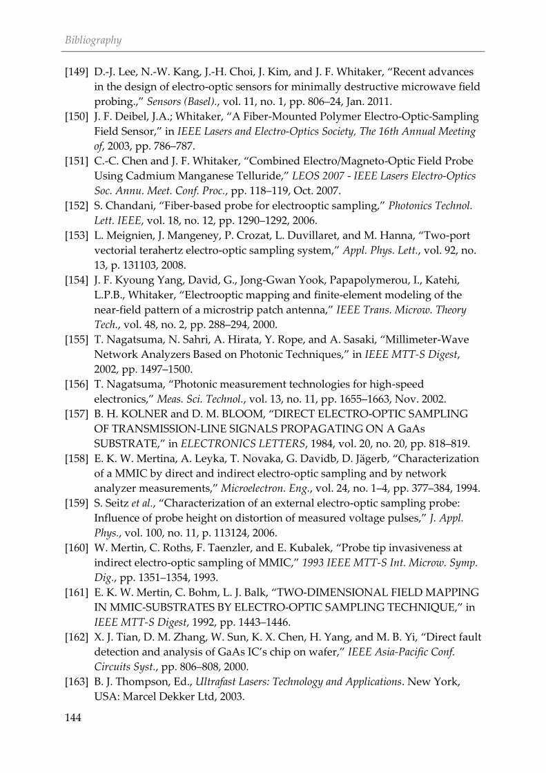
Bibliography
144
[149] D.-J. Lee, N.-W. Kang, J.-H. Choi, J. Kim, and J. F. Whitaker, “Recent advances
in the design of electro-optic sensors for minimally destructive microwave field
probing.,” Sensors (Basel)., vol. 11, no. 1, pp. 806–24, Jan. 2011.
[150] J. F. Deibel, J.A.; Whitaker, “A Fiber-Mounted Polymer Electro-Optic-Sampling
Field Sensor,” in IEEE Lasers and Electro-Optics Society, The 16th Annual Meeting
of, 2003, pp. 786–787.
[151] C.-C. Chen and J. F. Whitaker, “Combined Electro/Magneto-Optic Field Probe
Using Cadmium Manganese Telluride,” LEOS 2007 - IEEE Lasers Electro-Optics
Soc. Annu. Meet. Conf. Proc., pp. 118–119, Oct. 2007.
[152] S. Chandani, “Fiber-based probe for electrooptic sampling,” Photonics Technol.
Lett. IEEE, vol. 18, no. 12, pp. 1290–1292, 2006.
[153] L. Meignien, J. Mangeney, P. Crozat, L. Duvillaret, and M. Hanna, “Two-port
vectorial terahertz electro-optic sampling system,” Appl. Phys. Lett., vol. 92, no.
13, p. 131103, 2008.
[154] J. F. Kyoung Yang, David, G., Jong-Gwan Yook, Papapolymerou, I., Katehi,
L.P.B., Whitaker, “Electrooptic mapping and finite-element modeling of the
near-field pattern of a microstrip patch antenna,” IEEE Trans. Microw. Theory
Tech., vol. 48, no. 2, pp. 288–294, 2000.
[155] T. Nagatsuma, N. Sahri, A. Hirata, Y. Rope, and A. Sasaki, “Millimeter-Wave
Network Analyzers Based on Photonic Techniques,” in IEEE MTT-S Digest,
2002, pp. 1497–1500.
[156] T. Nagatsuma, “Photonic measurement technologies for high-speed
electronics,” Meas. Sci. Technol., vol. 13, no. 11, pp. 1655–1663, Nov. 2002.
[157] B. H. KOLNER and D. M. BLOOM, “DIRECT ELECTRO-OPTIC SAMPLING
OF TRANSMISSION-LINE SIGNALS PROPAGATING ON A GaAs
SUBSTRATE,” in ELECTRONICS LETTERS, 1984, vol. 20, no. 20, pp. 818–819.
[158] E. K. W. Mertina, A. Leyka, T. Novaka, G. Davidb, D. Jägerb, “Characterization
of a MMIC by direct and indirect electro-optic sampling and by network
analyzer measurements,” Microelectron. Eng., vol. 24, no. 1–4, pp. 377–384, 1994.
[159] S. Seitz et al., “Characterization of an external electro-optic sampling probe:
Influence of probe height on distortion of measured voltage pulses,” J. Appl.
Phys., vol. 100, no. 11, p. 113124, 2006.
[160] W. Mertin, C. Roths, F. Taenzler, and E. Kubalek, “Probe tip invasiveness at
indirect electro-optic sampling of MMIC,” 1993 IEEE MTT-S Int. Microw. Symp.
Dig., pp. 1351–1354, 1993.
[161] E. K. W. Mertin, C. Bohm, L. J. Balk, “TWO-DIMENSIONAL FIELD MAPPING
IN MMIC-SUBSTRATES BY ELECTRO-OPTIC SAMPLING TECHNIQUE,” in
IEEE MTT-S Digest, 1992, pp. 1443–1446.
[162] X. J. Tian, D. M. Zhang, W. Sun, K. X. Chen, H. Yang, and M. B. Yi, “Direct fault
detection and analysis of GaAs IC’s chip on wafer,” IEEE Asia-Pacific Conf.
Circuits Syst., pp. 806–808, 2000.
[163] B. J. Thompson, Ed., Ultrafast Lasers: Technology and Applications. New York,
USA: Marcel Dekker Ltd, 2003.
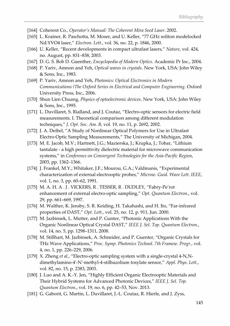
Bibliography
145
[164] Coherent Co., Operator’s Manual: The Coherent Mira Seed Laser. 2002.
[165] L. Krainer, R. Paschotta, M. Moser, and U. Keller, “77 GHz soliton modelocked
Nd:YVO4 laser,” Electron. Lett., vol. 36, no. 22, p. 1846, 2000.
[166] U. Keller, “Recent developments in compact ultrafast lasers,” Nature, vol. 424,
no. August, pp. 831–838, 2003.
[167] D. G. S. Bob D. Guenther, Encyclopedia of Modern Optics. Academic Pr Inc., 2004.
[168] P. Yariv, Amnon and Yeh, Optical waves in crystals. New York, USA: John Wiley
& Sons, Inc., 1983.
[169] P. Yariv, Amnon and Yeh, Photonics: Optical Electronics in Modern
Communications (The Oxford Series in Electrical and Computer Engineering. Oxford
University Press, Inc., 2006.
[170] Shun Lien Chuang, Physics of optoelectronic devices. New York, USA: John Wiley
& Sons, Inc., 1995.
[171] L. Duvillaret, S. Rialland, and J. Coutaz, “Electro-optic sensors for electric field
measurements. I. Theoretical comparison among different modulation
techniques,” J. Opt. Soc. Am. B, vol. 19, no. 11, p. 2692, 2002.
[172] J. A. Deibel, “A Study of Nonlinear Optical Polymers for Use in Ultrafast
Electro-Optic Sampling Measurements,” The University of Michigan, 2004.
[173] M. E. Jacob, M.V.; Hartnett, J.G.; Mazierska, J.; Krupka, J.; Tobar, “Lithium
tantalate - a high permittivity dielectric material for microwave communication
systems,” in Conference on Convergent Technologies for the Asia-Pacific Region,
2003, pp. 1362–1366.
[174] J. Frankel, M.Y.; Whitaker, J.F.; Mourou, G.A.; Valdmanis, “Experimental
characterization of external electrooptic probes,” Microw. Guid. Wave Lett. IEEE,
vol. 1, no. 3, pp. 60–62, 1991.
[175] M. A. H. A . J . VICKERS, R . TESSER, R . DUDLEY, “Fabry-Pe’rot
enhancement of external electro-optic sampling,” Opt. Quantum Electron., vol.
29, pp. 661–669, 1997.
[176] M. Walther, K. Jensby, S. R. Keiding, H. Takahashi, and H. Ito, “Far-infrared
properties of DAST,” Opt. Lett., vol. 25, no. 12, p. 911, Jun. 2000.
[177] M. Jazbinsek, L. Mutter, and P. Gunter, “Photonic Applications With the
Organic Nonlinear Optical Crystal DAST,” IEEE J. Sel. Top. Quantum Electron.,
vol. 14, no. 5, pp. 1298–1311, 2008.
[178] M. Stillhart, M. Jazbinsek, A. Schneider, and P. Guenter, “Organic Crystals for
THz Wave Applications,” Proc. Symp. Photonics Technol. 7th Framew. Progr., vol.
4, no. 1, pp. 226–229, 2006.
[179] X. Zheng et al., “Electro-optic sampling system with a single-crystal 4-N,N-
dimethylamino-4ʹ-Nʹ-methyl-4-stilbazolium tosylate sensor,” Appl. Phys. Lett.,
vol. 82, no. 15, p. 2383, 2003.
[180] J. Luo and A. K.-Y. Jen, “Highly Efficient Organic Electrooptic Materials and
Their Hybrid Systems for Advanced Photonic Devices,” IEEE J. Sel. Top.
Quantum Electron., vol. 19, no. 6, pp. 42–53, Nov. 2013.
[181] G. Gaborit, G. Martin, L. Duvillaret, J.-L. Coutaz, R. Hierle, and J. Zyss,
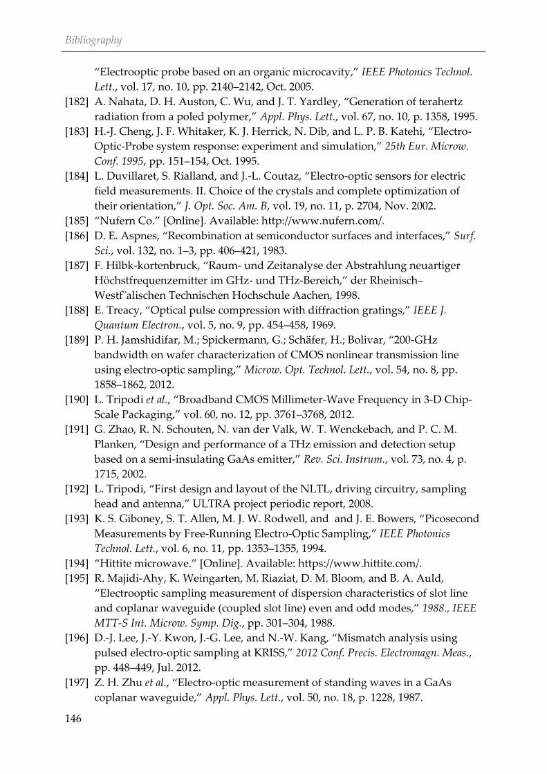
Bibliography
146
“Electrooptic probe based on an organic microcavity,” IEEE Photonics Technol.
Lett., vol. 17, no. 10, pp. 2140–2142, Oct. 2005.
[182] A. Nahata, D. H. Auston, C. Wu, and J. T. Yardley, “Generation of terahertz
radiation from a poled polymer,” Appl. Phys. Lett., vol. 67, no. 10, p. 1358, 1995.
[183] H.-J. Cheng, J. F. Whitaker, K. J. Herrick, N. Dib, and L. P. B. Katehi, “Electro-
Optic-Probe system response: experiment and simulation,” 25th Eur. Microw.
Conf. 1995, pp. 151–154, Oct. 1995.
[184] L. Duvillaret, S. Rialland, and J.-L. Coutaz, “Electro-optic sensors for electric
field measurements. II. Choice of the crystals and complete optimization of
their orientation,” J. Opt. Soc. Am. B, vol. 19, no. 11, p. 2704, Nov. 2002.
[185] “Nufern Co.” [Online]. Available: http://www.nufern.com/.
[186] D. E. Aspnes, “Recombination at semiconductor surfaces and interfaces,” Surf.
Sci., vol. 132, no. 1–3, pp. 406–421, 1983.
[187] F. Hilbk-kortenbruck, “Raum- und Zeitanalyse der Abstrahlung neuartiger
Höchstfrequenzemitter im GHz- und THz-Bereich,” der Rheinisch–
Westf¨alischen Technischen Hochschule Aachen, 1998.
[188] E. Treacy, “Optical pulse compression with diffraction gratings,” IEEE J.
Quantum Electron., vol. 5, no. 9, pp. 454–458, 1969.
[189] P. H. Jamshidifar, M.; Spickermann, G.; Schäfer, H.; Bolivar, “200-GHz
bandwidth on wafer characterization of CMOS nonlinear transmission line
using electro-optic sampling,” Microw. Opt. Technol. Lett., vol. 54, no. 8, pp.
1858–1862, 2012.
[190] L. Tripodi et al., “Broadband CMOS Millimeter-Wave Frequency in 3-D Chip-
Scale Packaging,” vol. 60, no. 12, pp. 3761–3768, 2012.
[191] G. Zhao, R. N. Schouten, N. van der Valk, W. T. Wenckebach, and P. C. M.
Planken, “Design and performance of a THz emission and detection setup
based on a semi-insulating GaAs emitter,” Rev. Sci. Instrum., vol. 73, no. 4, p.
1715, 2002.
[192] L. Tripodi, “First design and layout of the NLTL, driving circuitry, sampling
head and antenna,” ULTRA project periodic report, 2008.
[193] K. S. Giboney, S. T. Allen, M. J. W. Rodwell, and and J. E. Bowers, “Picosecond
Measurements by Free-Running Electro-Optic Sampling,” IEEE Photonics
Technol. Lett., vol. 6, no. 11, pp. 1353–1355, 1994.
[194] “Hittite microwave.” [Online]. Available: https://www.hittite.com/.
[195] R. Majidi-Ahy, K. Weingarten, M. Riaziat, D. M. Bloom, and B. A. Auld,
“Electrooptic sampling measurement of dispersion characteristics of slot line
and coplanar waveguide (coupled slot line) even and odd modes,” 1988., IEEE
MTT-S Int. Microw. Symp. Dig., pp. 301–304, 1988.
[196] D.-J. Lee, J.-Y. Kwon, J.-G. Lee, and N.-W. Kang, “Mismatch analysis using
pulsed electro-optic sampling at KRISS,” 2012 Conf. Precis. Electromagn. Meas.,
pp. 448–449, Jul. 2012.
[197] Z. H. Zhu et al., “Electro-optic measurement of standing waves in a GaAs
coplanar waveguide,” Appl. Phys. Lett., vol. 50, no. 18, p. 1228, 1987.
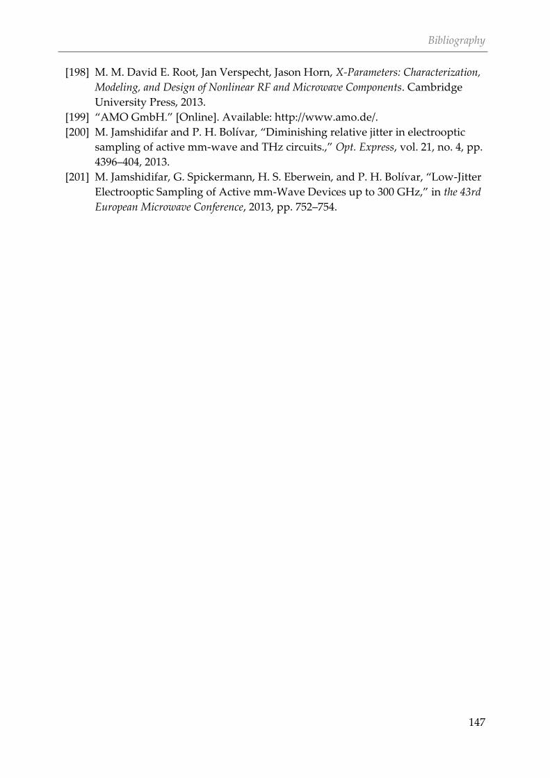
Bibliography
147
[198] M. M. David E. Root, Jan Verspecht, Jason Horn, X-Parameters: Characterization,
Modeling, and Design of Nonlinear RF and Microwave Components. Cambridge
University Press, 2013.
[199] “AMO GmbH.” [Online]. Available: http://www.amo.de/.
[200] M. Jamshidifar and P. H. Bolívar, “Diminishing relative jitter in electrooptic
sampling of active mm-wave and THz circuits.,” Opt. Express, vol. 21, no. 4, pp.
4396–404, 2013.
[201] M. Jamshidifar, G. Spickermann, H. S. Eberwein, and P. H. Bolívar, “Low-Jitter
Electrooptic Sampling of Active mm-Wave Devices up to 300 GHz,” in the 43rd
European Microwave Conference, 2013, pp. 752–754.

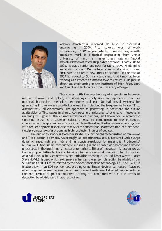
Mehran Jamshidifar received his B.Sc. in electrical engineering in 2000. After several years of work experience, in 2005 he graduated with master degree with excellent mark in electrical engineering from Urmia University of Iran. His master thesis was on fractal miniaturization of microstrip patch antennas. From 2005 to 2008, he was a senior engineer for radio networks planning and optimization in Mobile Telecommunication Co. of Iran. Enthusiastic to learn new areas of science, in the end of 2008 he moved to Germany and since that time has been working as a research assistant towards his Ph. D degree in electrical engineering in the Institute of High Frequency and Quantum Electronics at the University of Siegen.
THz waves, with the electromagnetic spectrum between millimeter-waves and optics, are nowadays widely used in applications such as material inspection, medicine, astronomy and etc. Optical based systems for generating THz waves are usually bulky and inefficient at the frequencies below 1THz. Alternatively, all-electronics THz approach is promising to facilitate the future availability of THz waves in cheap, compact and industrial solutions. A milestone in reaching this goal is the characterization of devices, and therefore, electrooptic sampling (EOS) is a superior solution. EOS, in comparison to the electronic characterization approaches offers a much broadband and faster measurement system with reduced systematic errors from system calibrations. Moreover, non-contact near-field probing allows for producing high resolution images of devices. The aim of this work is to demonstrate EOS for the characterization of mm-wave and THz electronic devices. Accordingly, an experimental setup, featured with a large dynamic range, high sensitivity, and high spatial resolution for imaging is introduced. A 65-nm CMOS Nonlinear Transmission Line (NLTL) is then chosen as a broadband device under test. In the preliminary measurement phase, jitter of the system is recognized as the major prohibiting factor in achieving a full measurement bandwidth for the device. As a solution, a fully coherent synchronization technique, called Laser Master Laser Slave (LM-LS) is used which extremely enhances the system detection bandwidth from 50 GHz up to 300 GHz, restricted by the device fabrication technology i.e., the CMOS. It is also shown that EOS non-contact probing of nonlinear devices can detect features which may not be seen by electronic measurement instrumentation at device ports. In the end, results of photoconductive probing are compared with EOS in terms of detection bandwidth and image resolution.