Embed Size (px)
Citation preview
Phase Separation in Thin Polymer Films:
From Self Stratification to
Polymer Blend Lithography
genehmigte Inauguraldissertation
Zur Erlangung des akademischen Grades eines
DOKTORS DER NATURWISSENSCHAFTEN
im Fachbereich Material- und Geowissenschaften der Technischen Universität Darmstadt
vorgelegte von
Cheng Huang Master of Science
aus Shanghai
1. Referent: Prof. Dr. Horst Hahn 2. Referent: Prof. Dr. Thomas Schimmel Prüfer: Prof. Dr. Robert Stark Prüfer: Prof. Dr. Ralf Riedel
Tag der Einreichung: 07. August 2014 Tag der mündlichen Prüfung: 18. Dezember 2014
Darmstadt 2015 D 17


Schriftliche Erklärung Gemäß § 9 der Promotionsordnung zur Erlangung des akademischen Grades eines Doktors der Naturwissenschaften (Dr. rer. nat.) der Technischen Universität Darmstadt. Hiermit erkläre ich, dass ich die vorliegende Dissertation selbständig verfasst und ausschließlich die in der Arbeit angegebenen Hilfsmittel verwendet habe. Ich versichere weiterhin, dass dies mein erster Promotionsversuch ist. Darmstadt, 18.04.2014

Zusammenfassung Diese Arbeit beschreibt das Phasenverhalten in dünnen Polymerfilmen, die durch Spincoating einer Polymerlösung zweier inkompatibler Polymere (Polystyrol (PS) und Poly¬methylmethacrylat (PMMA)) hergestellt werden. Bei Lösungen in Methylethylketon (MEK) kann sich – abhängig von den experimentellen Bedingungen – eine rein laterale Struktur oder ein horizontal geschichteter Aufbau der Polymerphasen einstellen. Die Strukturbildung ist dabei abhängig von einer Vielzahl von Parametern: dem Massenverhältnis der Polymere, der Verdampfungsrate, dem Molekelurgewicht, der Polymere und von der relativen Luftfeuchtigkeit in der Prozessgasatmosphäre über dem Spincoater. Die Luftfeuchte ist es, die dabei ganz wesentlich den Übergang zwischen Selbststratifikation und lateraler Strukturbildung bestimmt. Die Dynamik der Schichtbildung wurde, abhängig von den oben genannten Parametern, durch optische Echtzeit-In-situ-Reflektometrie und die entstehenden Morphologien mit Rasterelektronenemikroskopie (REM) bzw. Rasterkraftmikroskopie (AFM) untersucht. Wird die Lösung in reiner (trockener) Stickstoffatmosphäre aufgesponnen, bildet sich eine Dreifachschicht mit der Schichtfolge: PMMA/PS/PMMA, was durch Ellipsometrie und Sekundärionenmassenspektroskopie (SIMS) nachgewiesen wurde. Ein diffusionsdominiertes Strukturbildungsmodell, welches die Wechselwirkung mit dem polaren Substrat (SiOx) und mit der Restfeuchtigkeit in der Polymerlösung bzw. der Atmosphäre berücksichtigt, erklärt dieses Verhalten der inkompatiblen Polymere. Ein erweitertes Modell beschreibt die Strukturbildung bei höherer Luftfeuchtigkeit. Bei einer relativen Feuchte von 40-50 %, bildet sich stets ein dünner PMMA-Film der isolierte PS Inseln oder Tröpfchen enthält. Laut dem Modell bilden sich diese Inseln oder Tröpfchen fern von der Grenzfläche im Inneren des Filmes. Durch Entnetzen des PMMA-Filmes unter- und oberhalb der Tröpfchen liegen diese am Ende des Trocknungsvorgangs auf dem Substrat auf und haben gleichzeitig Kontakt zur Luftgrenzfläche. Daher können nun durch Verwendung eines selektiven Lösungsmittels entweder PS oder PMMA aufgelöst werden um das Substrat an den vom jeweiligen Polymer bedeckten Stellen freizulegen. Diese Vorgehensweise bezeichnen wir als Polymer-Blend-Lithographie und demonstrieren in dieser Arbeit zwei Ausführungen davon: 1. Die „Monolagen-Polymer-Blend¬Lithographie“ (Monolayer PBL), wo eine Abbild der Polymerstruktur in einer selbst-organisierenden Monolage entsteht, sowie 2. Die „Metal PBL“ wo eine aufgedampfte Metallschicht lateral strukturiert wird. Dabei entstehen mesoskopische Metallinseln (Abhängig von den gewählten Parametern 50 nm bis 500 nm Durchmesser) oder großflächige Metallfilme mit mesoskopischen Poren gleicher Größe mit einer typischen Dichte von 1 Milliarde / 2,5 cm x 2,5 cm. Neben der erfolgreichen Anwendung der gemusterten Monolagen als Template für ortsselektive Mineralisation von Zinkoxid-Inseln (ZnO) wurde schließlich die wellenlängenselektive Transmission aufgrund der plasmonischen Eigenschaften der Metallfilme demonstriert.

Abstract This thesis describes the self-stratification as well as the purely lateral phase separation in a thin polymer blend film during spin coating. The solution system consists of polystyrene (PS) and poly(methyl methacrylate) (PMMA) in methylethylketon (MEK) as the solvent. It is shown that the formation of the morphology during spin-coating is influenced by a variety of parameters. These are the PS/PMMA mass ratio, the evaporation rate of MEK, the molecular weights (of PS and PMMA) and the humidity of the spin casting atmosphere. The dynamic of the layer formation was monitored by optical real-time in-situ reflectometry and the final morphologies were characterized by Scanning Electron Microscopy (SEM) and Atomic Force Microscopy (AFM). According to the model established in this study, the spin-casting humidity is the most important factor in determination of the phase separation ranging from layering to lateral phase separation between the two immiscible polymers. In (dry) nitrogen flow the PS/PMMA/MEK system forms a triple layer film following our „self-stratification model“. The sandwich-like triple layer (PMMA/PS/PMMA) was proven by different techniques including ellipsometry and Secondary Ion Mass Spectrometry (SIMS). With another model we describe the formation of a purely lateral phase morphology, where PS islands are separated in a PMMA matrix. Here, at a humidity of 40-50 %, this 3-dimensional phase separation occurs, whereby self-stratification was observed at lower humidity. Since the PS islands have contact both to the air and the substrate, this purely lateral morphology can be utilized in a novel lithographic technique, which we named „Polymer Blend Lithography (PBL)“ [1,2]. Using a selective solvent, one or the other polymer can be removed and the remaining one can then be used as a lithographic mask for a subsequent lift off process. If e.g. the PS Islands are removed a perforated PMMA film is left, which we call the “Swiss Cheese Structure”. In this study, two examples of the applications of PBL are demonstrated: 1. The fabrication of nano-patterned organic Self-Assembled Monolayer (SAM) templates, which we call Monolayer PBL and 2. Metal PBL which is specialized for the fabrication of micro/nanosized metal island arrays or perforated metal films with a typical hole density of 1 billion / inch2
. These nanopatterned templates can be applied e.g. for surface-selective mineralization of ZnO films. Finally the wavelength-selective transmission of perforated aluminum films, which is based on the surface plasmonic effect, is demonstrated.


Abbreviations
AFM Atomic Force Microscope
APTES (3-Aminopropyl)triethoxysilane
FDTS 1H,1H,2H,2H -perfluorodecyl Trichlorosilane
DDW Double Distilled Water
LFM Lateral Force Mode
MEK Methylethylketon
PBL Polymer Blend Lithography
PMMA Poly(methyl methacrylate)
PS Polystyrene
PT Polythiophene
PTFE Polytetrafluorethylen
PVP Poly(2-vinylpyredine)
SEM Scanning Electron Microscope
SIMS Secondary Ion Mass Spectroscopy
THF Tetrahydrofuran

i
Content
1. INTRODUCTION ....................................................................................................................... 1
2. THEORY ..................................................................................................................................... 3
2.1 FUNDAMENTALS OF POLYMER PHYSICS .............................................................................. 32.1.1 Some Basic Concepts of Polymer Science .......................................................................... 3
2.1.2 The Flory-Huggins Theory ................................................................................................. 5
2.1.3 Phase Separation in Polymer Blend .................................................................................. 8
2.2 WETTING AND DEWETTING ............................................................................................... 102.3 ULTRA THIN ORGANIC FILMS ............................................................................................... 13
2.3.1 Self Assembled Monolayer (SAM) ..................................................................................... 13
2.3.2 Polystyrene Brush .............................................................................................................. 15
2.4 INTERFERENCE OF LIGHT ON MULTILAYER FILM ................................................................. 16
3. PREPARATION METHODS .................................................................................................. 19
3.1 THE PREPARATION OF POLYMER FILMS ................................................................................ 193.1.1 Substrate Cleaning Techniques ......................................................................................... 19
3.1.2 The Polymer Blend Solution .............................................................................................. 21
3.1.3 The Humidity-Regulated Spin-Coating Technique .......................................................... 22
3.1.4 The Selective Solvents ........................................................................................................ 25
3.2 METAL FILM DEPOSITION WITH THERMAL EVAPORATION TECHNIQUE ............................... 263.3 THE PREPARATION OF SILANE SAMS IN GAS PHASE ............................................................ 273.4 THE PREPARATION OF PS BRUSH .......................................................................................... 28
4. CHARACTERIZATION METHODS .................................................................................... 29
4.1 OPTICAL MICROSCOPE .......................................................................................................... 294.2 SCANNING ELECTRON MICROSCOPE (SEM) ......................................................................... 294.3 ATOMIC FORCE MICROSCOPE ............................................................................................... 31
4.3.1 General Construction of AFM ........................................................................................... 31
4.3.2 Interactions between Samples and Cantilevers ................................................................ 33
4.3.3 The Contact Mode .............................................................................................................. 34
4.3.4 The Tapping Mode ............................................................................................................. 35
4.3.5 Analysis of Grain Size Distribution. ................................................................................. 36
4.4 TIME RESOLVED REFLECTOMETER ....................................................................................... 364.5 ELLIPSOMETER ...................................................................................................................... 404.6 TIME-OF-FLIGHT SECONDARY ION MASS SPECTROMETRY ................................................... 41
5. PHASE SEPARATION IN THIN PS/PMMA FILM: FROM SELF-STRATIFICATION TO PURELY LATERAL PHASE SEPARATION .................................................................... 43
5.1 SELF STRATIFICATION OF PS/PMMA IN NITROGEN ENVIRONMENT .................................... 43
ii
5.2 DEPENDENCE OF MORPHOLOGY ON SPIN-CASTING HUMIDITY ............................................ 515.3 SELF STRATIFICATION – PURELY LATERAL PHASE SEPARATION MODEL ............................. 55
5.3.1 Self Stratification in Nitrogen Flow .................................................................................. 55
5.3.2 From Self Stratification to Purely Lateral Phase Separation ......................................... 57
5.4 RESULTS OF TIME RESOLVED REFLECTOMETRY ............................................................... 615.5 REPRODUCTION OF THE PURELY LATERAL PHASE SEPARATION ON PS/PVP/MEK SYSTEM 695.6 SUMMARY ............................................................................................................................. 73
6. THE PURELY LATERAL PHASE SEPARATION IN THIN POLYMER BLEND FILM OF PS/PMMA ............................................................................................................................... 75
6.1 INFLUENCES OF MASS RATIO ON THE MORPHOLOGY ........................................................... 766.2 INFLUENCES OF ROTATION SPEED ON THE MORPHOLOGY .................................................... 836.3 INFLUENCES OF EVAPORATION RATE ON THE MORPHOLOGY ............................................... 876.4 INFLUENCES OF PS MOLECULAR WEIGHT ON THE MORPHOLOGY ........................................ 936.5 THE DYNAMIC PROCESS OF THE MORPHOLOGY FORMATION ............................................... 996.6 SUMMARY ........................................................................................................................... 105
7. FABRICATION OF ORGANIC SELF ASSEMBLED MONOLAYER (SAM) TEMPLATES VIA POLYMER BLEND LITHOGRAPHY (MONOLAYER-PBL) ........... 109
7.1 FABRICATION OF 2-PHASE TEMPLATES ............................................................................... 1107.2 APPLICATION OF MONOLAYER-PBL FOR LATERAL CONTROLLED GROWTH OF ZNO FILMS
VIA CHEMICAL BATH DEPOSITION ............................................................................................ 1157.3 FABRICATION OF 3-PHASE TEMPLATES ............................................................................... 1167.4 SUMMARY AND PERSPECTIVES ........................................................................................... 119
8. FABRICATION OF METALS ISLAND ARRAYS OR PERFORATED METAL FILMS WITH PBL (METAL-PBL) ....................................................................................................... 121
8.1 FABRICATION OF METAL ISLANDS OR PERFORATED FILMS ................................................ 1218.2 FABRICATION OF SUB-100 NM HOLES AND ISLANDS .......................................................... 1248.3 WAVELENGTH SELECTIVITY OF PERFORATED AL FILMS .................................................... 1258.4 SUMMARY AND PERSPECTIVES ........................................................................................... 127
9. CONCLUSIONS ..................................................................................................................... 129
FROM SELF STRATIFICATION TO PURELY LATERAL PHASE SEPARATION ................................. 129POLYMER BLEND LITHOGRAPHY: MONOLAYER–PBL AND METAL-PBL ................................ 133
REFERENCES ............................................................................................................................ 135
1
1. Introduction
Phase separation of binary polymer blend solutions during a spin-coating process produces nano and micro patterns on large areas in a fast and upscalable fashion. This phase separation has been intensively studied over the past two decades and allows the formation of complex layered or lateral micro- or nanoscale structures [3-22]. It is possible to guide the morphogenesis by a pre-patterned solid template in order to form layout-defined structures [23-26]. These structures can be used for many applications such as anti-reflection coatings
In this study PS/PMMA blend was spun-cast from methylethylketon (MEK) in nitrogen flow and a triple layer film is found. The middle layer of PS contains nanosized PMMA tunnels which expand with the increase of the humidity. At a critical humidity the structure is formed with a different mechanism and shows a purely lateral phase separation, which means the blend separates completely into two lateral phases. This means that the PS droplets are formed in a PMMA matrix, whereby both phases have contact to the substrate as well as to the air. In this study a controlling parameter was identified which can be adjusted to either yield a purely vertical or a purely lateral morphology after spin-casted from the same polymer solution. This is especially remarkable because this crucial parameter is humidity, which is typically not kept constant or even not mentioned in nearly the entire literature existing about thin polymer films. The purely lateral phase separation opens
[27], photovoltaic devices [28, 29], organic light emitting diodes (OLED) [30-32] and more. Different from the annealing of the bulk material of thin polymer films at elevated temperatures [19-21, 33], the phase separation initiated by solvent evaporation involves complex and non-equilibrium processes [11, 18, 22]. Heriot et al developed a time resolved reflectometer to investigate the evaporation process of the solvent during spin-coating [17, 18, 22]. His colleagues Mokarian-Tabari et al made use of this equipment to study the morphology of PS/PMMA blend solution spun-cast at controlled evaporation rate of solvent, which was achieved by applying the corresponding humidity of the solvent [22]. Jaczewska et al studied humidity and solvent effects on the phase separation between Polythiophene (PT) and PS blend [11]. The solvents applied in these studies include toluene, chloroform and tetrahydrofuran (THF). All of these scientists put forward models explaining the formation of the morphologies via a transient double layer state, which then often transforms into a lateral structure at the film-air interface, whereby one component always completely wets the substrate-film interface. This situation is very often found when polymer blend films are cast from solutions and could be named as a semi-lateral or semi-horizontal phase separation. In some rare cases a purely horizontal phase separation could be found [3, 23]. To the best of our knowledge neither a purely lateral phase separation nor a triple-layer vertical phase separation has been yet reported.
2
the possibility of lithographic application – remove one component with selective solvent and used the other as a lithographic mask. The technique here is named as Polymer Blend Lithography (PBL) and is divided into Monolayer-PBL and Metal-PBL according to the material of the fabricated nanopatterns.
Monolayer Polymer-Blend-Lithography (Monolayer-PBL) is a versatile and reliable method to fabricate large scale nano-patterned Self-Assembled Monolayers (SAM) [1, 2]. SAMs have been studied intensively for many years [34-37]. Patterning of self-assembled monolayers on the nanometer scale was performed by sequential lithographic techniques such as Electron beam lithography [38, 39] or scanning force microscopy-based lithographic techniques [40-46]. The advantage of techniques such as electron beam lithography or SFM-based lithography is their high lateral resolution and their reproducibility – their major disadvantage is the fact that they rely on sequential writing processes which are very time consuming and need expensive equipment. For patterning larger areas on the nanometer scale – e.g. for the fabrication of nanopatterned, biofunctional templates – easy-to-use, cheap and fast techniques allowing the parallel fabrication of billions of nanostructures are required. In such cases, PBL technique can be a good alternative to the traditional ones.
Metal Polymer Blend Lithography (Metal-PBL) is a rapid, cost-effective and promising way to fabricate a micro/nanosized metal islands arrays and perforated metal films [129]. It is a good alternative technique to nano sphere lithography [47-49], laser interference lithography [50, 51], AFM based dip-pen lithography [52] and more.
This work focuses on introducing the purely lateral phase separation between PS and PMMA when spun-cast from MEK. Various parameters including the mass ratio between the two polymers, evaporation rate of the solvent, molecular weight of the polymers are discussed and finally a qualitative model of the formation of such morphology is established. The applications of PBL on nano-patterned SAMs as well as micro/nano-sized metal island arrays or perforated metal films are also introduced.
3
2. Theory
2.1 Fundamentals of Polymer Physics
2.1.1 Some Basic Concepts of Polymer Science
Polymers are chain molecules, consisting of a great number of repeating units (monomers). The number of the repeating units N is called the degree of polymerization. For synthetic polymers N ranges from 100 to a few ten thousand. Chain molecules with N less than 100 are called oligomers. In general the backbone incorporates silicon, nitrogen or oxygen with a variety of side groups connected to them. The bulk material of polymer is normally a melt or an amorphous or partially crystalline solid. The polymers can be classified in many ways. According to its degree of cross-linking between the molecules, the polymers can be divided into thermoplastics, elastomers and thermosets. The thermoplastics are with no or very low density of cross-links and therefore the bulk material is relatively soft. All the recyclable polymers we use in our daily life are thermoplastics. The best representative of an elastomer is rubber, which has a medium degree of cross-linking. The cross-links among the molecules contribute the high elasticity of the bulk material. The polymer material becomes rigid and more stable against high temperature when the molecules are closely cross-linked. These polymers are called thermosets. When the chain consists of only one kind of monomer, the polymer is called a homopolymer while a heteropolymer consists of more kinds of monomers. There is a special kind of heteropolymer which is called block copolymer. It consists of two or more head-to-tail connected homopolymer or homo oligomer blocks [53, 54].
The developing polymer chemistry produces a manifold of different substances of high complexity with a broad range of material properties. But by far more complex polymers are created by the nature. They include proteins, polysaccharides (e.g. cellulose but also chitin), natural rubber (polyisoprene) and many others [55]. The polymers used in this study are common technical polymers which are commercially available, such as polystyrene (PS) or poly(methylmethacrylate) (PMMA), which is known as the plexiglas.
Since the degree of the polymerization N cannot be constant for all the molecules during the production of synthetic polymers. The molecular weight of polymers is not an absolute value but a molecular weight distribution. The most common expressions of the polymer molecular weight are the weight average molecular weight Mw and the number average molecular weight Mn
which are defined as
4
𝑀𝑛 =∑ 𝑁𝑖𝑀𝑖𝑖∑ 𝑁𝑖𝑖
𝑀𝑤 =∑ 𝑊𝑖𝑀𝑖𝑖∑ 𝑊𝑖𝑖
where Ni is the number of molecules with molecular weight Mi and Wi the total weight of molecules with molecular weight Mi
Since M
. The distribution of the molecular weight is described by the polydispersity index D, defined in equation 3.3 [53].
𝐷 =𝑀𝑤
𝑀𝑛
w > Mn
the large the value of D is, the wider the distribution of the molecular weight of the polymer is. The molecular weight of for example, the PS and PMMA used in the study ranges from several to a few hundred kg/mol, interpreted in contour length a few to a few hundred nanometers, which means the molecular weight of polymers have a very wide distribution in the normal case. For our studies all polymers were purchased from the Polymer Standards from where polymers with very low D (typically 1.10 or even less) are provided. Since a variety of polymer properties depend strongly on its molecular length, it is important to use this special kind of polymer.
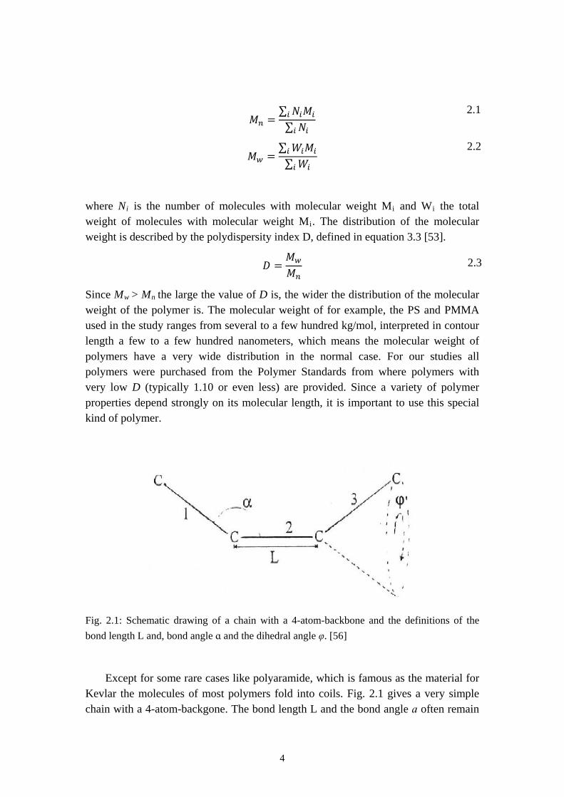
Fig. 2.1: Schematic drawing of a chain with a 4-atom-backbone and the definitions of the bond length L and, bond angle ɑ and the dihedral angle φ. [56]
Except for some rare cases like polyaramide, which is famous as the material for Kevlar the molecules of most polymers fold into coils. Fig. 2.1 gives a very simple chain with a 4-atom-backgone. The bond length L and the bond angle ɑ often remain
2.1
2.2
2.3
5
constant while the dimension of the dihedral angle φ is free due to the interactions between the different side groups which are bond to the backbone. When the chain becomes longer, the molecule will coil itself into thousands or even millions of different configurations. If the end-to-end distance follows the Gaussian distribution, the coil is considered as a Gaussian coil. The dimension of the polymer chain will be described by the radius of gyration RG,
𝑅𝐺 = √𝐶𝐿2𝑁
which is the root mean square distance of the atoms of the chain from the center of gravity of the chain:
where C is an empirical constant. The proportional dependence of RG on N1/2 is only for the case of amorphous polymer above glass transition temperature Tg. At temperature below Tg
the diffusion of the entire molecular chain is strongly suppressed due to the less free volume which decreases together with the temperature. Thus the polymer material becomes rigid and brittle [56, 57].
2.1.2 The Flory-Huggins Theory
The general idea put forward by Flory and Huggins enables us to deal with the mixing properties of a pair of polymers and provides a basic understanding of the occurrence of different types of phase diagrams, in dependence on temperature and the molecular weights. The change in Gibbs free energy is considered in order to study the mixing properties of two polymers:
∆𝐺𝑚𝑖𝑥 = 𝐺𝐴𝐵 − (𝐺𝐴 + 𝐺𝐵)
where 𝐺𝐴, 𝐺𝐵 and 𝐺𝐴𝐵 represent the Gibbs free energy of polymer A with degree of polymerization , polymer B with in separate states and the mixed state and the mixture of A and B [56,57].
The Flory-Huggins treatment considers that ∆𝐺𝑚𝑖𝑥 is the sum of two components:
∆𝐺𝑚𝑖𝑥 = ∆𝐻 − 𝑇∆𝑆
where ∆𝐻 is the change of enthalpy, ∆𝑆 the change of entropy and 𝑇 the temperature. The ∆𝑆 is normally favorable as the mixing increases the entropy while ∆𝐻 may act favorably or unfavorably, depending on the character of the monomer-monomer pair interactions and other facts like the shrinkage or expansion of the total volume [57]. With the help of mean field treatment, the change of enthalpy can be written as the equations below:
∆𝐻 = 𝑛𝑘𝐵𝑇𝜒𝜑𝐴𝜑𝐵
where 𝑛 is the total number of monomers, 𝑘𝐵 the Boltzmann constant, 𝜑𝐴 and 𝜑𝐵 are the volume fractions of the two components and The Flory-Huggins parameter 𝜒 is dimensionless and determines empirically the change of interactions between different
2.4
2.5
2.6
2.7
6
monomers compared to identical monomers. Since the entropy is determined as the product of Boltzmann constant and the number of possible conformations of the molecule 𝛺, where
𝑆 = 𝐾𝐵𝑙𝑛𝛺
The change of the entropy in mixing can be written as:
∆𝑆 = −𝑛𝑘𝐵 �𝜑𝐴
𝑁𝐴𝑙𝑛𝜑𝐴+
𝜑𝐵𝑁𝐵𝑙𝑛𝜑𝐵
�
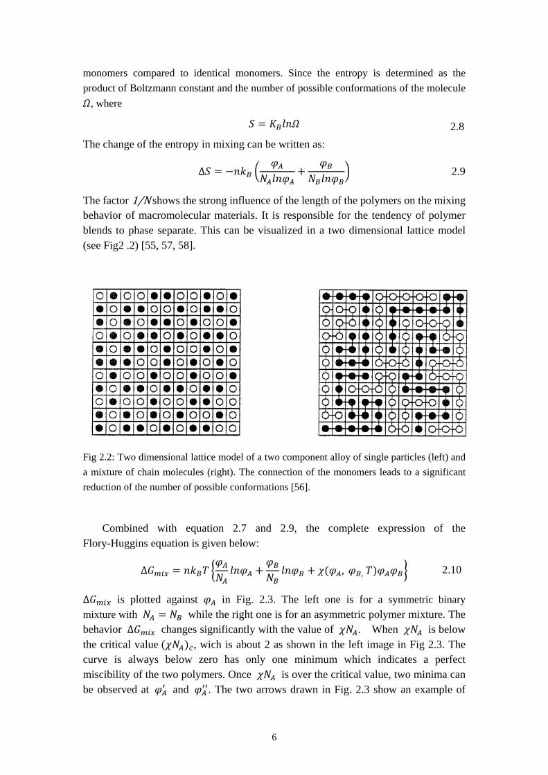
The factor 1/N shows the strong influence of the length of the polymers on the mixing behavior of macromolecular materials. It is responsible for the tendency of polymer blends to phase separate. This can be visualized in a two dimensional lattice model (see Fig2 .2) [55, 57, 58].
Fig 2.2: Two dimensional lattice model of a two component alloy of single particles (left) and a mixture of chain molecules (right). The connection of the monomers leads to a significant reduction of the number of possible conformations [56].
Combined with equation 2.7 and 2.9, the complete expression of the Flory-Huggins equation is given below:
∆𝐺𝑚𝑖𝑥 = 𝑛𝑘𝐵𝑇 �𝜑𝐴𝑁𝐴
𝑙𝑛𝜑𝐴 +𝜑𝐵𝑁𝐵
𝑙𝑛𝜑𝐵 + 𝜒(𝜑𝐴, 𝜑𝐵, 𝑇)𝜑𝐴𝜑𝐵�
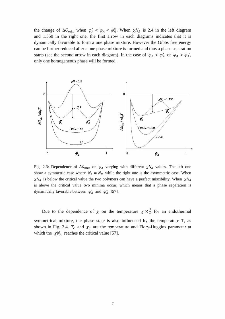
∆𝐺𝑚𝑖𝑥 is plotted against 𝜑𝐴 in Fig. 2.3. The left one is for a symmetric binary mixture with 𝑁𝐴 = 𝑁𝐵 while the right one is for an asymmetric polymer mixture. The behavior ∆𝐺𝑚𝑖𝑥 changes significantly with the value of 𝜒𝑁𝐴. When 𝜒𝑁𝐴 is below the critical value (𝜒𝑁𝐴)𝑐, wich is about 2 as shown in the left image in Fig 2.3. The curve is always below zero has only one minimum which indicates a perfect miscibility of the two polymers. Once 𝜒𝑁𝐴 is over the critical value, two minima can be observed at 𝜑𝐴′ and 𝜑𝐴′′. The two arrows drawn in Fig. 2.3 show an example of
2.9
2.8
2.10
7
the change of ∆𝐺𝑚𝑖𝑥 when 𝜑𝐴′ < 𝜑𝐴 < 𝜑𝐴′′. When 𝜒𝑁𝐴 is 2.4 in the left diagram and 1.550 in the right one, the first arrow in each diagrams indicates that it is dynamically favorable to form a one phase mixture. However the Gibbs free energy can be further reduced after a one phase mixture is formed and thus a phase separation starts (see the second arrow in each diagram). In the case of 𝜑𝐴 < 𝜑𝐴′ or 𝜑𝐴 > 𝜑𝐴′′, only one homogeneous phase will be formed.
Fig. 2.3: Dependence of ∆𝐺𝑚𝑖𝑥 on 𝜑𝐴 varying with different 𝜒𝑁𝐴 values. The left one show a symmetric case where 𝑁𝐴 = 𝑁𝐵 while the right one is the asymmetric case. When 𝜒𝑁𝐴 is below the critical value the two polymers can have a perfect miscibility. When 𝜒𝑁𝐴 is above the critical value two minima occur, which means that a phase separation is dynamically favorable between 𝜑𝐴′ and 𝜑𝐴′′ [57].
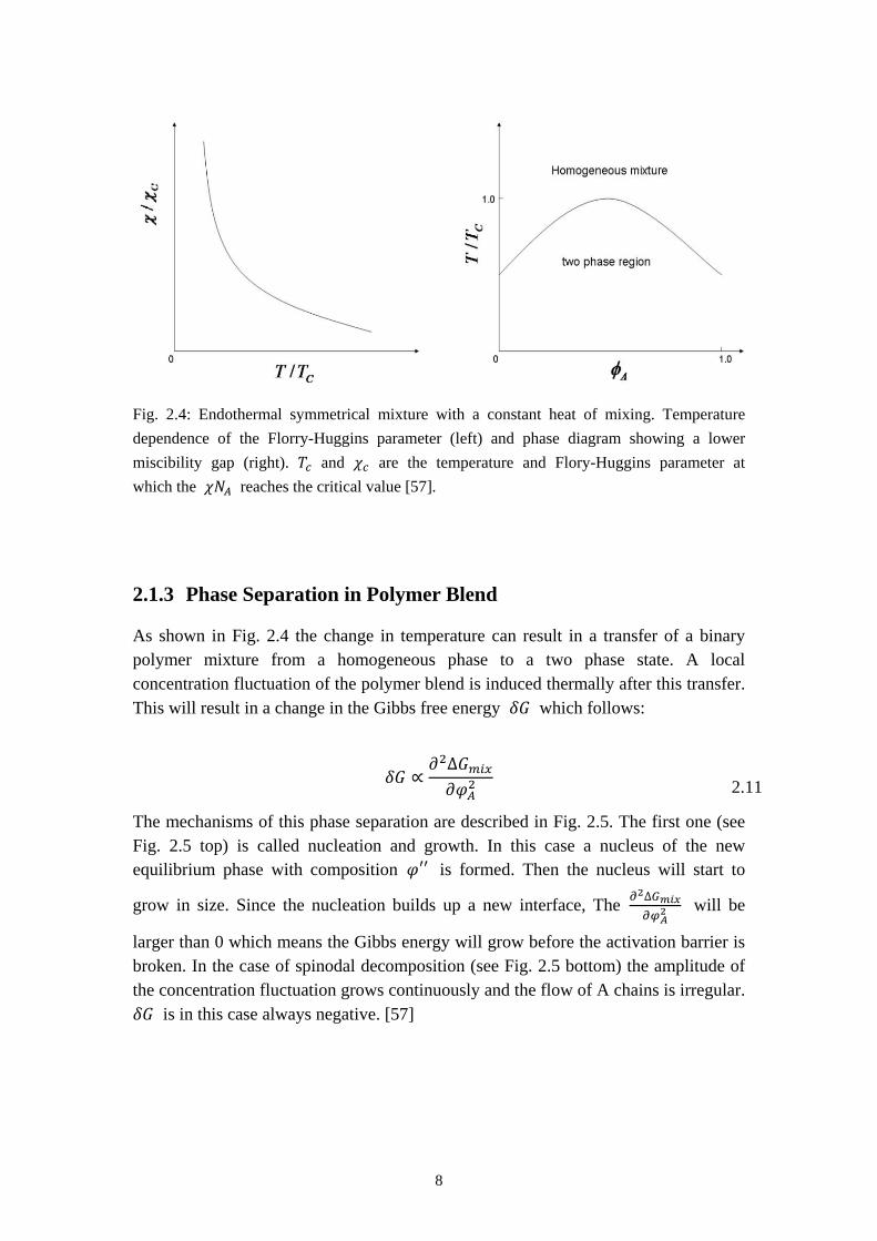
Due to the dependence of 𝜒 on the temperature 𝜒 ∝ 1𝑇
for an endothermal
symmetrical mixture, the phase state is also influenced by the temperature T, as shown in Fig. 2.4. 𝑇𝑐 and 𝜒𝑐 are the temperature and Flory-Huggins parameter at which the 𝜒𝑁𝐴 reaches the critical value [57].
8
Fig. 2.4: Endothermal symmetrical mixture with a constant heat of mixing. Temperature dependence of the Florry-Huggins parameter (left) and phase diagram showing a lower miscibility gap (right). 𝑇𝑐 and 𝜒𝑐 are the temperature and Flory-Huggins parameter at which the 𝜒𝑁𝐴 reaches the critical value [57].
2.1.3 Phase Separation in Polymer Blend
As shown in Fig. 2.4 the change in temperature can result in a transfer of a binary polymer mixture from a homogeneous phase to a two phase state. A local concentration fluctuation of the polymer blend is induced thermally after this transfer. This will result in a change in the Gibbs free energy 𝛿𝐺 which follows:
𝛿𝐺 ∝𝜕2∆𝐺𝑚𝑖𝑥
𝜕𝜑𝐴2
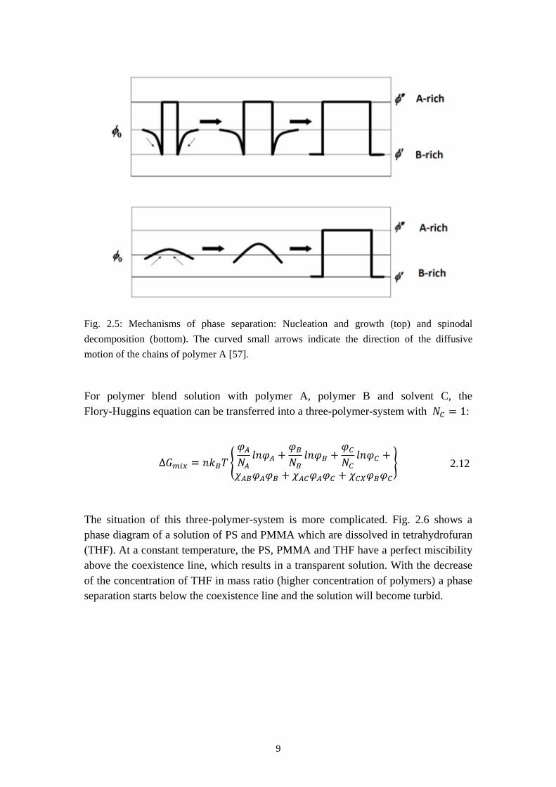
The mechanisms of this phase separation are described in Fig. 2.5. The first one (see Fig. 2.5 top) is called nucleation and growth. In this case a nucleus of the new equilibrium phase with composition 𝜑′′ is formed. Then the nucleus will start to
grow in size. Since the nucleation builds up a new interface, The 𝜕2∆𝐺𝑚𝑖𝑥𝜕𝜑𝐴
2 will be
larger than 0 which means the Gibbs energy will grow before the activation barrier is broken. In the case of spinodal decomposition (see Fig. 2.5 bottom) the amplitude of the concentration fluctuation grows continuously and the flow of A chains is irregular. 𝛿𝐺 is in this case always negative. [57]
2.11
9
Fig. 2.5: Mechanisms of phase separation: Nucleation and growth (top) and spinodal decomposition (bottom). The curved small arrows indicate the direction of the diffusive motion of the chains of polymer A [57].
For polymer blend solution with polymer A, polymer B and solvent C, the Flory-Huggins equation can be transferred into a three-polymer-system with 𝑁𝐶 = 1:
∆𝐺𝑚𝑖𝑥 = 𝑛𝑘𝐵𝑇 �𝜑𝐴𝑁𝐴
𝑙𝑛𝜑𝐴 +𝜑𝐵𝑁𝐵
𝑙𝑛𝜑𝐵 +𝜑𝐶𝑁𝐶
𝑙𝑛𝜑𝐶 +
𝜒𝐴𝐵𝜑𝐴𝜑𝐵 + 𝜒𝐴𝐶𝜑𝐴𝜑𝐶 + 𝜒𝐶𝑋𝜑𝐵𝜑𝐶�
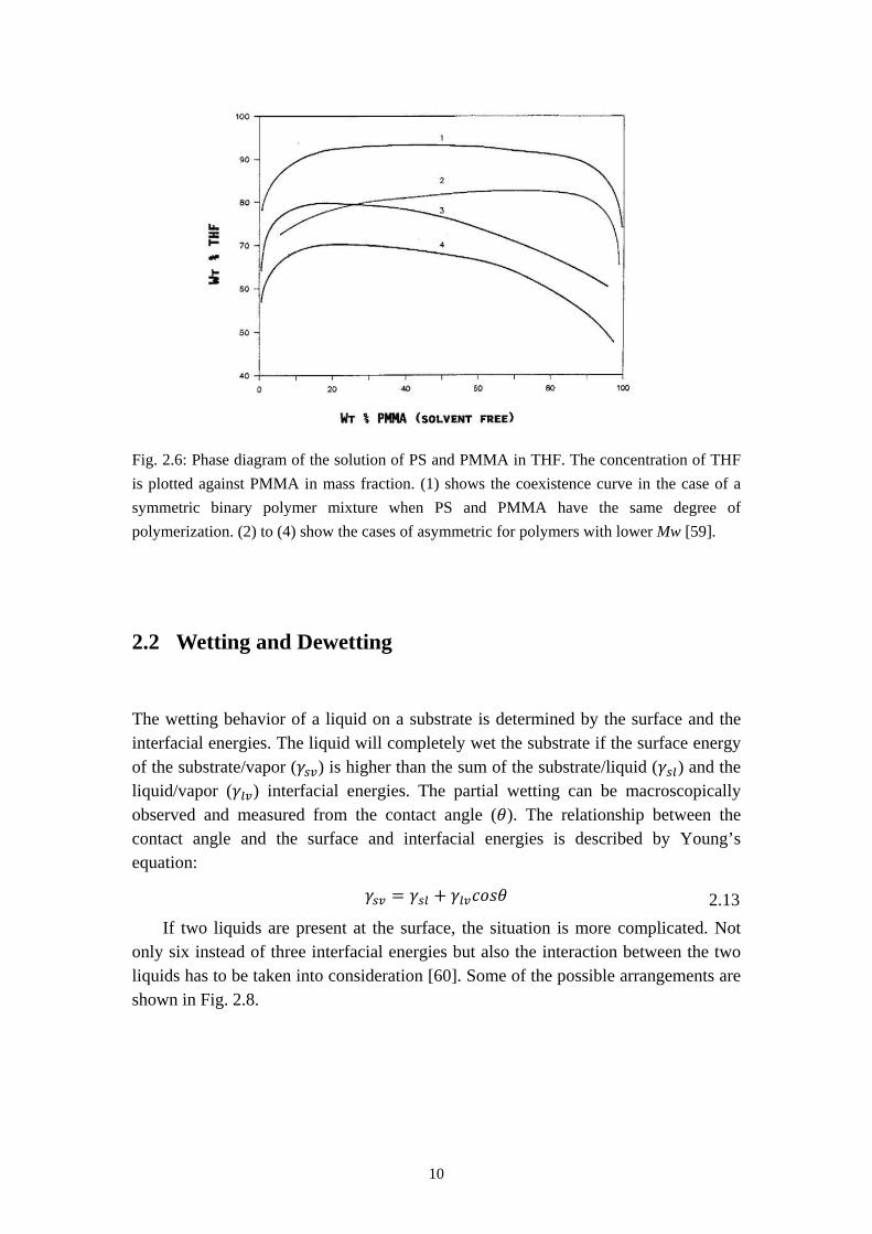
The situation of this three-polymer-system is more complicated. Fig. 2.6 shows a phase diagram of a solution of PS and PMMA which are dissolved in tetrahydrofuran (THF). At a constant temperature, the PS, PMMA and THF have a perfect miscibility above the coexistence line, which results in a transparent solution. With the decrease of the concentration of THF in mass ratio (higher concentration of polymers) a phase separation starts below the coexistence line and the solution will become turbid.
2.12
10
Fig. 2.6: Phase diagram of the solution of PS and PMMA in THF. The concentration of THF is plotted against PMMA in mass fraction. (1) shows the coexistence curve in the case of a symmetric binary polymer mixture when PS and PMMA have the same degree of polymerization. (2) to (4) show the cases of asymmetric for polymers with lower Mw [59].
2.2 Wetting and Dewetting
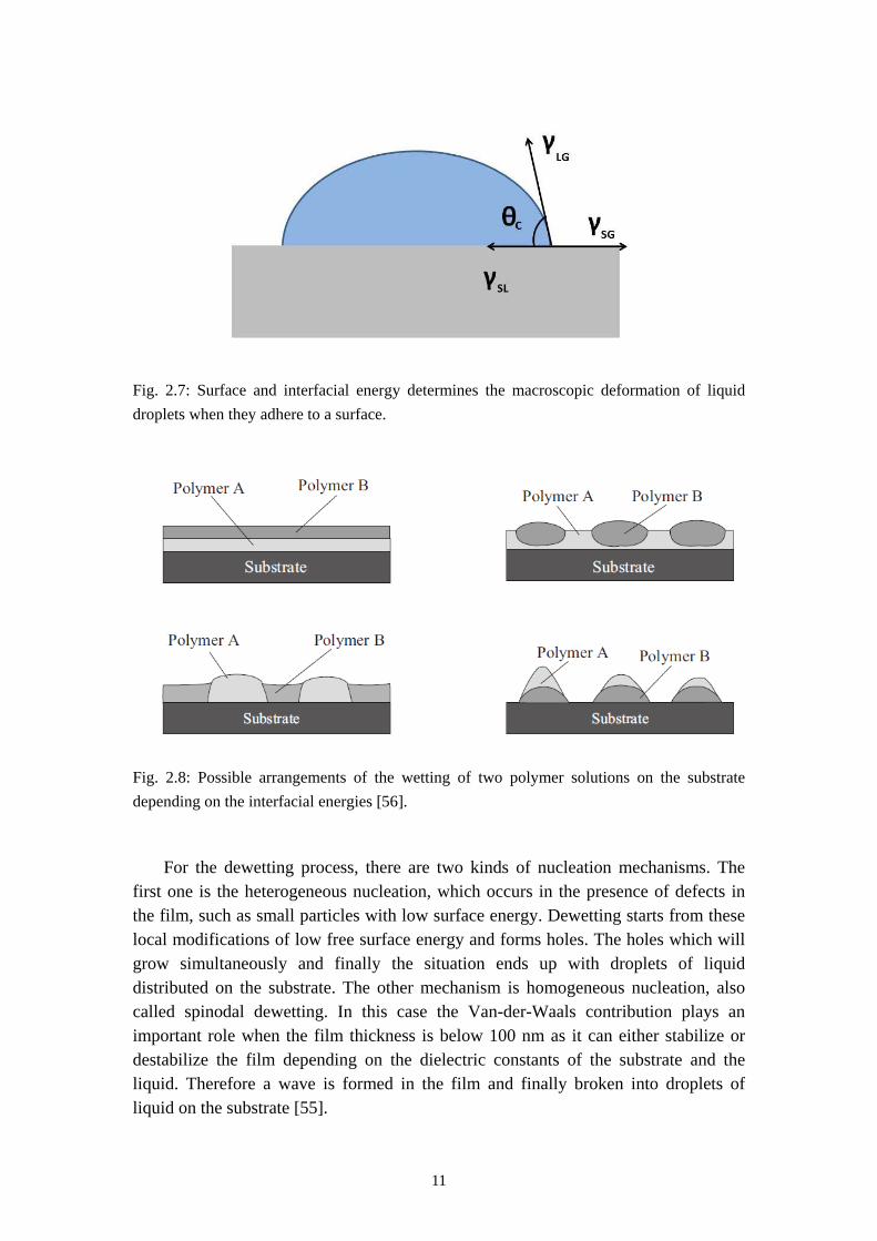
The wetting behavior of a liquid on a substrate is determined by the surface and the interfacial energies. The liquid will completely wet the substrate if the surface energy of the substrate/vapor (𝛾𝑠𝑣) is higher than the sum of the substrate/liquid (𝛾𝑠𝑙) and the liquid/vapor (𝛾𝑙𝑣) interfacial energies. The partial wetting can be macroscopically observed and measured from the contact angle (𝜃). The relationship between the contact angle and the surface and interfacial energies is described by Young’s equation:
𝛾𝑠𝑣 = 𝛾𝑠𝑙 + 𝛾𝑙𝑣𝑐𝑜𝑠𝜃
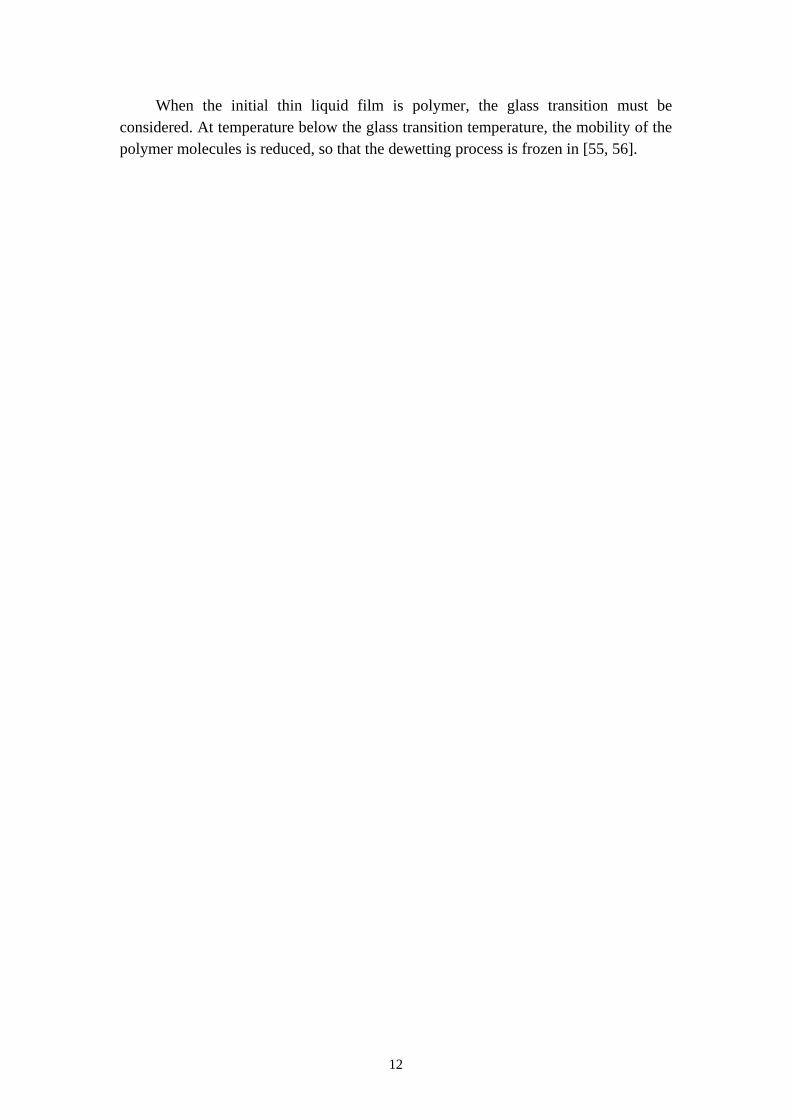
If two liquids are present at the surface, the situation is more complicated. Not only six instead of three interfacial energies but also the interaction between the two liquids has to be taken into consideration [60]. Some of the possible arrangements are shown in Fig. 2.8.
2.13
11
Fig. 2.7: Surface and interfacial energy determines the macroscopic deformation of liquid droplets when they adhere to a surface.
Fig. 2.8: Possible arrangements of the wetting of two polymer solutions on the substrate depending on the interfacial energies [56].
For the dewetting process, there are two kinds of nucleation mechanisms. The first one is the heterogeneous nucleation, which occurs in the presence of defects in the film, such as small particles with low surface energy. Dewetting starts from these local modifications of low free surface energy and forms holes. The holes which will grow simultaneously and finally the situation ends up with droplets of liquid distributed on the substrate. The other mechanism is homogeneous nucleation, also called spinodal dewetting. In this case the Van-der-Waals contribution plays an important role when the film thickness is below 100 nm as it can either stabilize or destabilize the film depending on the dielectric constants of the substrate and the liquid. Therefore a wave is formed in the film and finally broken into droplets of liquid on the substrate [55].
12
When the initial thin liquid film is polymer, the glass transition must be considered. At temperature below the glass transition temperature, the mobility of the polymer molecules is reduced, so that the dewetting process is frozen in [55, 56].
13
2.3 Ultra-Thin Organic Films
Organic monolayers have a series of properties, which are interesting for many applications. They can be used for further chemical modification or used for constructive lithographic processes [61]. The preparation of such a monolayer as it is formed after adsorption to the surface under a self-assembling process. In this study two kinds of organic monolayers, Self-Assembled Monolayer (SAM) and polymer brush were fabricated
2.3.1 Self Assembled Monolayer (SAM)
Due to the affiliation of the head group to the substrate the special kind of molecules can form a monolayer after adsorption from a self-organized process. The monolayer is therefore called a Self-Assembled Monolayer (SAM). A SAM molecule normally consisted of a head group, a backbone and an end group. The most common head groups are thiol (-SH) which binds to metal surfaces, such as gold or silver or chlorosilane (-SiCl3) which binds to silicon or silicon oxide surfaces. The backbone is normally an alkane chain, which is the main part of a SAM molecule. The end group on the other hand can be “selected” according to the application requirement. For example, a hydrophilic surface can be turned into a hydrophobic one by the deposition of a SAM with an –CH3
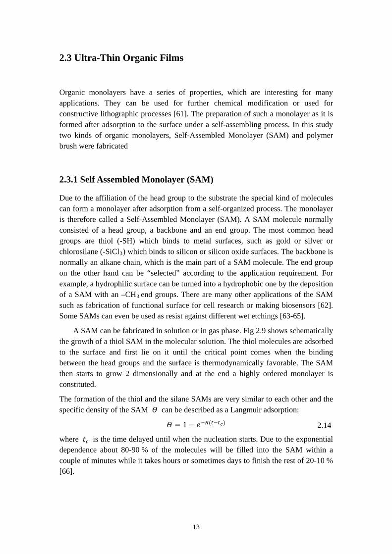
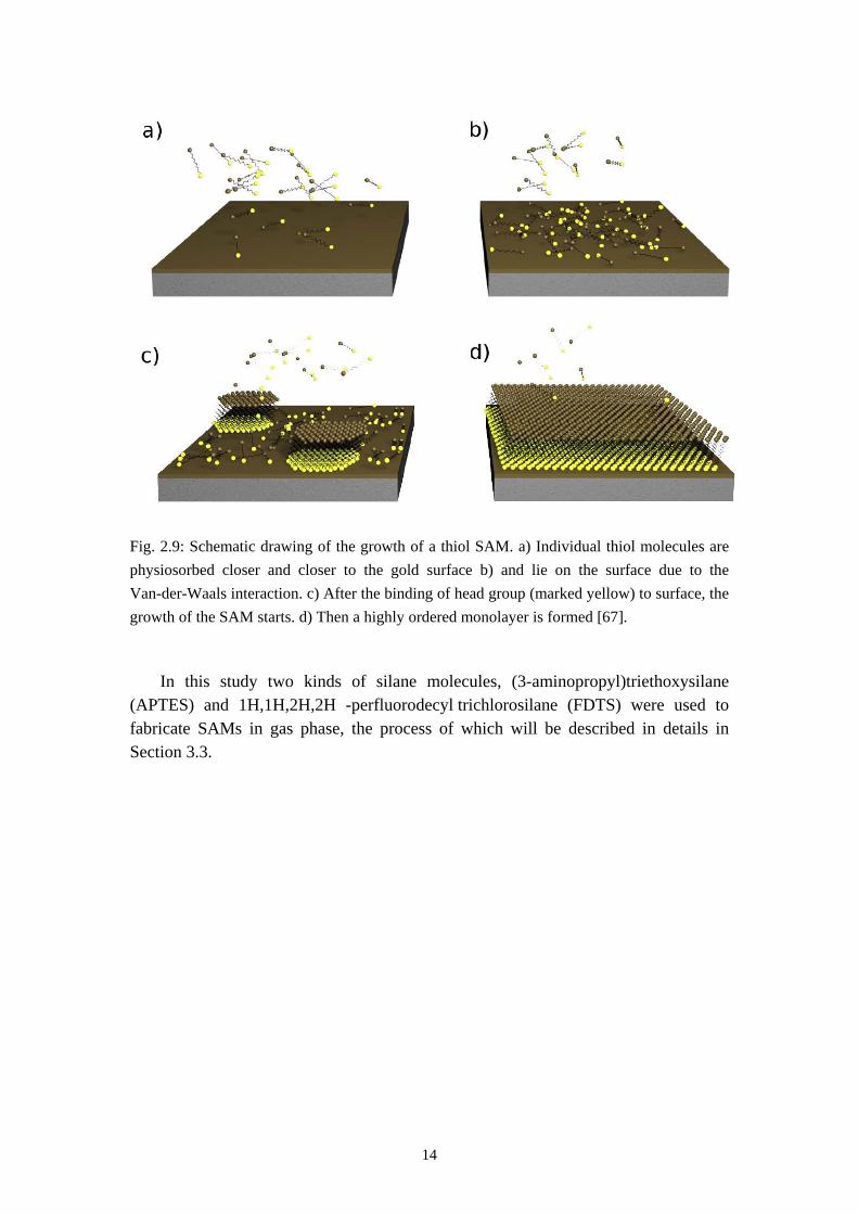
A SAM can be fabricated in solution or in gas phase. Fig 2.9 shows schematically the growth of a thiol SAM in the molecular solution. The thiol molecules are adsorbed to the surface and first lie on it until the critical point comes when the binding between the head groups and the surface is thermodynamically favorable. The SAM then starts to grow 2 dimensionally and at the end a highly ordered monolayer is constituted.
end groups. There are many other applications of the SAM such as fabrication of functional surface for cell research or making biosensors [62]. Some SAMs can even be used as resist against different wet etchings [63-65].
The formation of the thiol and the silane SAMs are very similar to each other and the specific density of the SAM 𝛳 can be described as a Langmuir adsorption:
𝛳 = 1 − 𝑒−𝑅(𝑡−𝑡𝑐)
where 𝑡𝑐 is the time delayed until when the nucleation starts. Due to the exponential dependence about 80-90 % of the molecules will be filled into the SAM within a couple of minutes while it takes hours or sometimes days to finish the rest of 20-10 % [66].
2.14
14
Fig. 2.9: Schematic drawing of the growth of a thiol SAM. a) Individual thiol molecules are physiosorbed closer and closer to the gold surface b) and lie on the surface due to the Van-der-Waals interaction. c) After the binding of head group (marked yellow) to surface, the growth of the SAM starts. d) Then a highly ordered monolayer is formed [67].
In this study two kinds of silane molecules, (3-aminopropyl)triethoxysilane (APTES) and 1H,1H,2H,2H -perfluorodecyl trichlorosilane (FDTS) were used to fabricate SAMs in gas phase, the process of which will be described in details in Section 3.3.
15
2.3.2 Polystyrene Brush
By binding to the surface with their reactive head groups polymer molecules can form a brush-like monolayer on the surface of the substrate. Due to the difference in the contour length between polymer and SAM molecules a polymer brush is normally softer. Instead of standing on the substrate like SAM molecules, the polymer chains partially lie on the surface. As for the surface fictionalization the SAM molecules contribute only their end groups while the whole polymer chain can be regarded as a bunch of head groups.
The fabrication of a polymer brush surface can be achieved in two ways. The first one is called “grafting to”, which means that the polymer molecules with reactive head groups are bond to the substrate surface via certain reactions normally in liquid phase. The other way is first to cover the surface of the substrate with a layer of initiators and then start the polymerization directly from them in a monomer solution, which is thus called “grafting from” method [68-73].
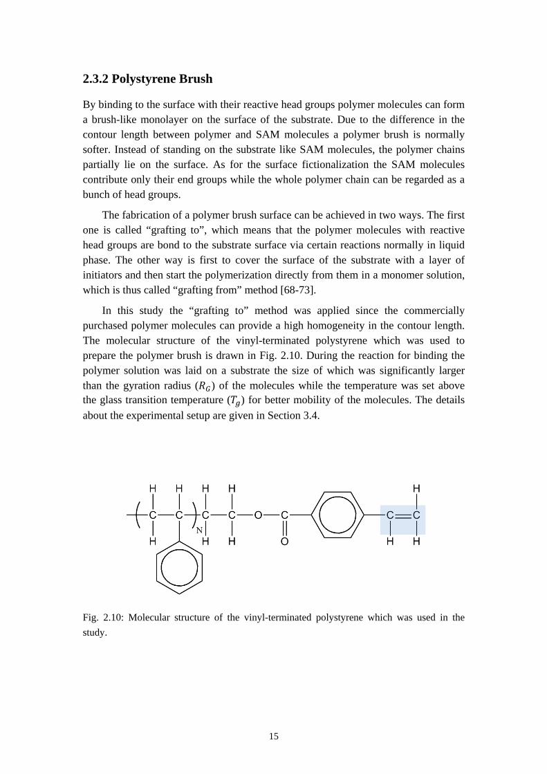
In this study the “grafting to” method was applied since the commercially purchased polymer molecules can provide a high homogeneity in the contour length. The molecular structure of the vinyl-terminated polystyrene which was used to prepare the polymer brush is drawn in Fig. 2.10. During the reaction for binding the polymer solution was laid on a substrate the size of which was significantly larger than the gyration radius (𝑅𝐺) of the molecules while the temperature was set above the glass transition temperature (𝑇𝑔) for better mobility of the molecules. The details about the experimental setup are given in Section 3.4.
Fig. 2.10: Molecular structure of the vinyl-terminated polystyrene which was used in the study.
16
2.4 Interference of Light on Multilayer Film
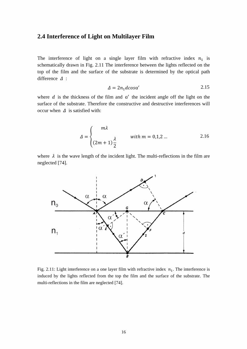
The interference of light on a single layer film with refractive index 𝑛1 is schematically drawn in Fig. 2.11 The interference between the lights reflected on the top of the film and the surface of the substrate is determined by the optical path difference 𝛥 :
𝛥 = 2𝑛1𝑑𝑐𝑜𝑠ɑ′
where 𝑑 is the thickness of the film and ɑ′ the incident angle off the light on the surface of the substrate. Therefore the constructive and destructive interferences will occur when 𝛥 is satisfied with:
𝛥 = �
𝑚𝜆
(2𝑚 + 1)𝜆2
𝑤𝑖𝑡ℎ 𝑚 = 0,1,2 … �
where 𝜆 is the wave length of the incident light. The multi-reflections in the film are neglected [74].
Fig. 2.11: Light interference on a one layer film with refractive index 𝑛1. The interference is induced by the lights reflected from the top the film and the surface of the substrate. The multi-reflections in the film are neglected [74].
2.15
2.16
17
In the case of the interference of light on a multi-layer film, the transfer matrix M is introduced. For a film with only one layer:
𝑀1 = �𝑚11 𝑚12𝑚21 𝑚22
� = � 𝑐𝑜𝑠𝜑 𝑖𝑠𝑖𝑛𝜑𝛾1
𝑖𝛾1 𝑠𝑖𝑛𝜑 𝑐𝑜𝑠𝜑�
where 𝑖 is the imaginary unit, 𝜑 is the phase angle which is defined as :
𝜑 = 2𝜋𝜆0
𝑛1 𝑑 𝑐𝑜𝑠 ɑ1
where 𝜆0 is the wavelength of the incident light, 𝑛1 the refractive index of the first layer, d the thickness of the whole film and ɑ1 the incident angle of the light on the surface of the first layer. The 𝛾 parameter is defined as:
𝛾𝑖 = 𝑛𝑖𝑐0
𝑐𝑜𝑠 ɑ𝑖
where 𝑐0 the speed of light in vacuum and 𝑛𝑖 and ɑ𝑖 are the refractive index and the incident angle of light on layer i. The sum of the transfer matrix of the multi-layer film 𝑀𝑇 is given as :
𝑀𝑇 = 𝑀1𝑀2𝑀3 … 𝑀𝑖
Then comes the reflection factor 𝑟U:
𝑟 = 𝛾0𝑚11 + 𝛾0𝛾𝑠𝑚12 − 𝑚21 − 𝛾𝑠𝑚22
𝛾0𝑚11 + 𝛾0𝛾𝑠𝑚12 + 𝑚21 + 𝛾𝑠𝑚22
where 𝛾𝑠 and 𝛾0are the 𝛾 parameters of the substrate and the transmission media from which the light comes to the multi-layer film. Thus the reflection grade 𝑅 can be calculated:
𝑅 = �𝑟�2 [74]
In this study the calculation of the reflection grade 𝑅 was used to simulate the development of a triple layer film during spin-casting.
2.17
2.18
2.19
2.20
2.21
2.22

18
19
3. Preparation Methods
3.1 The Preparation of Polymer Films
3.1.1 Substrate Cleaning Techniques
Silicon wafers and glass slides were used as substrates in the experiments for polymer films. An oxide layer with thickness at about 2 nm is formed on silicon wafer surface due to the exposure to oxygen in the air. The wafers and glass were incised into small pieces, typically 1.5 x 1.5 and 2 x 2 cm2
The Snow Jet Cleaning Technique
. Two cleaning techniques, the snow jet cleaning and the RCA 1 cleaning were applied depending on the properties of the substrates.
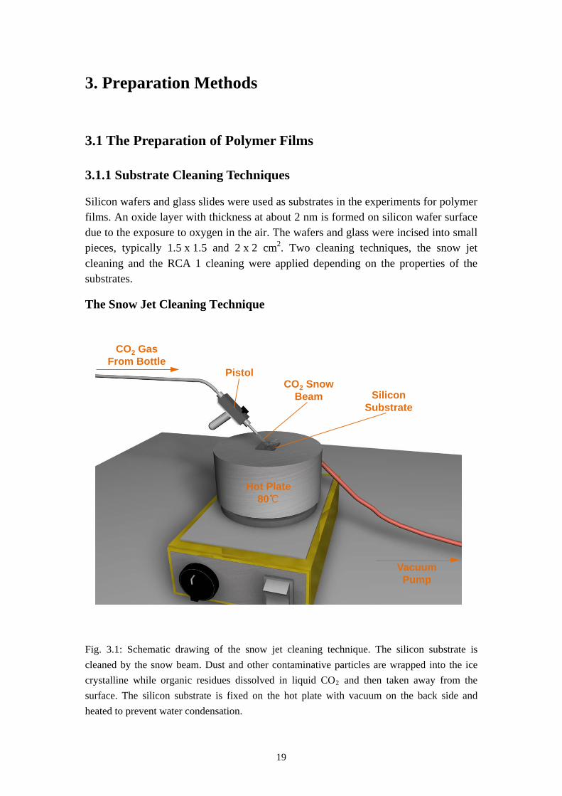
Fig. 3.1: Schematic drawing of the snow jet cleaning technique. The silicon substrate is cleaned by the snow beam. Dust and other contaminative particles are wrapped into the ice crystalline while organic residues dissolved in liquid CO2
CO2 Gas From Bottle
Vacuum Pump
Hot Plate80℃
Pistol
Silicon Substrate
CO2 Snow Beam
and then taken away from the surface. The silicon substrate is fixed on the hot plate with vacuum on the back side and heated to prevent water condensation.
20
As shown in Fig. 3.1, a CO2 flow under pressure at about 58.5 bars comes out from the nozzle of the pistol which is held about 1 cm above the surface of the silicon substrate. The temperature of the gas decreases rapidly due to its expansion and therefore, a CO2 ice crystalline beam, or a snow beam is formed (snow jet) when it reaches the substrate surface. The snow beam cleans the surface both mechanically and chemically. Dust or other contaminative particles are wrapped into the ice crystalline while the organic residues are dissolved in the liquid CO2
On the aluminum block of the hot plate there is a small opening which connected to a vacuum pump in order to fix the silicon substrate from the back side. The sample is heated during the cleaning process in order to prevent water condensation. [75-77]
and then taken away from the substrate surface.
The snow jet cleaning technique was used in the experiments as a standard cleaning process for all silicon substrates supporting polymer films and silicon samples with organic monolayer and also a lift off technique to remove polymer films.
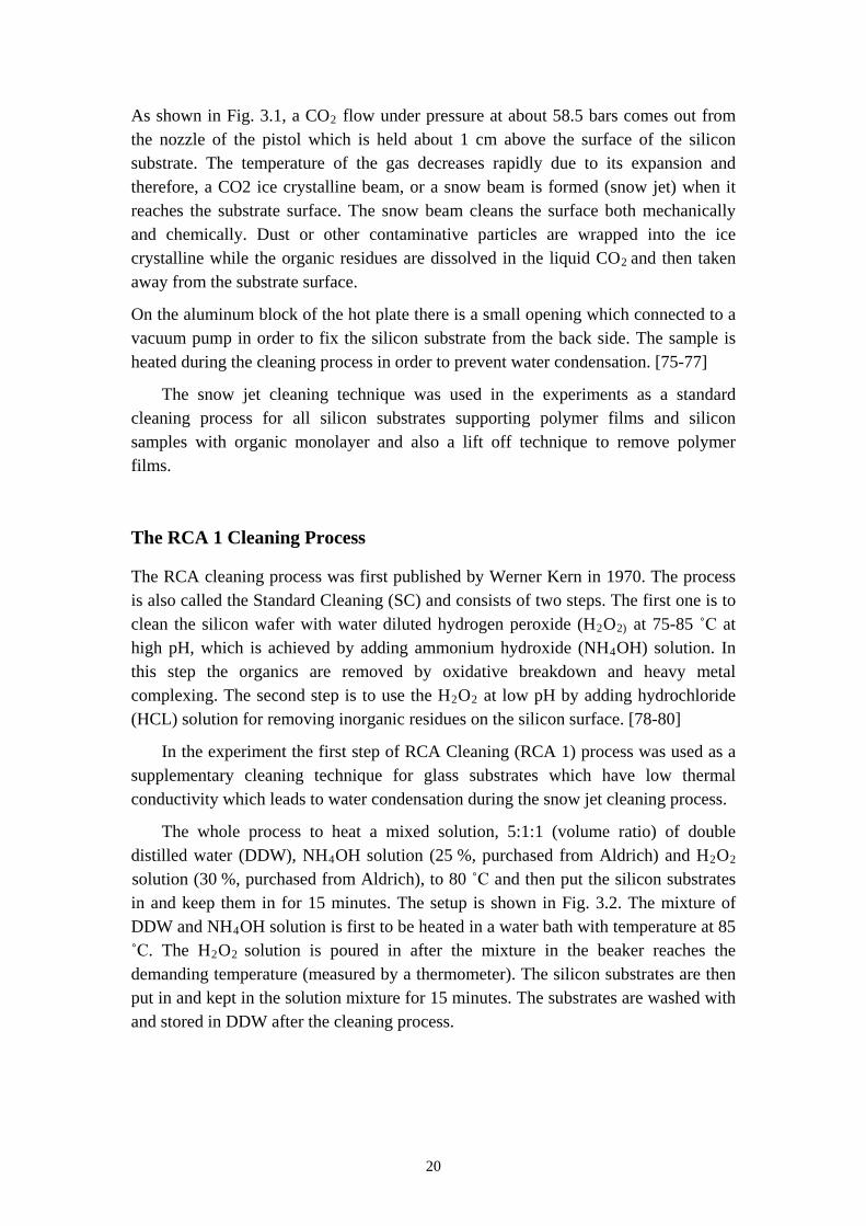
The RCA 1 Cleaning Process
The RCA cleaning process was first published by Werner Kern in 1970. The process is also called the Standard Cleaning (SC) and consists of two steps. The first one is to clean the silicon wafer with water diluted hydrogen peroxide (H2O2) at 75-85 ˚C at high pH, which is achieved by adding ammonium hydroxide (NH4OH) solution. In this step the organics are removed by oxidative breakdown and heavy metal complexing. The second step is to use the H2O2
In the experiment the first step of RCA Cleaning (RCA 1) process was used as a supplementary cleaning technique for glass substrates which have low thermal conductivity which leads to water condensation during the snow jet cleaning process.
at low pH by adding hydrochloride (HCL) solution for removing inorganic residues on the silicon surface. [78-80]
The whole process to heat a mixed solution, 5:1:1 (volume ratio) of double distilled water (DDW), NH4OH solution (25 %, purchased from Aldrich) and H2O2
solution (30 %, purchased from Aldrich), to 80 ˚C and then put the silicon substrates in and keep them in for 15 minutes. The setup is shown in Fig. 3.2. The mixture of DDW and NH4OH solution is first to be heated in a water bath with temperature at 85 ˚C. The H2O2
solution is poured in after the mixture in the beaker reaches the demanding temperature (measured by a thermometer). The silicon substrates are then put in and kept in the solution mixture for 15 minutes. The substrates are washed with and stored in DDW after the cleaning process.
21
Fig. 3.2: Schematic drawing of RCA 1 cleaning process. The substrates are put in a mixed solution of NH4OH (25 %), H2O2
(30 %) and DDW (volume ration 1:1:5), heated up to about 80˚C by a water bath and kept there for 15 minutes.
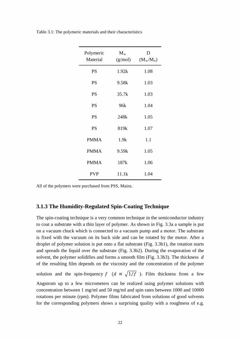
3.1.2 The Polymer Blend Solution
In this study so-called standard polymers, which feature a narrow molecular weight distribution were used, in other word with a very low polydispersity index D. The polymers used in the study are polystyrene (PS), poly(methyl methacrylate) (PMMA) and poly(2-vinylpyredine) (PVP). Their molecular structures are drawn in Fig. 3.3 while the characteristics of are listed in Table 3.1. The molecular weights of the polymers mentioned in this work are always the weight average molecular weight Mw.
The polymers were used as purchased (from Polymer Standard Service (PSS)). The polymer blends are described by the mass ratio between the two mixed polymers. After the polymers being dissolved in solvents, the solution was filtered with syringe filter equipped with 0.2 μm polytetrafluorethylen (PTFE) membrane, which was purchased from VWR International.
22
Table 3.1: The polymeric materials and their characteristics
Polymeric Material
Mw
D (M(g/mol) w/Mn)
PS 1.92k 1.08
PS 9.58k 1.03
PS 35.7k 1.03
PS 96k 1.04
PS 248k 1.05
PS 819k 1.07
PMMA 1.9k 1.1
PMMA 9.59k 1.05
PMMA 187k 1.06
PVP 11.1k 1.04
All of the polymers were purchased from PSS, Mainz.
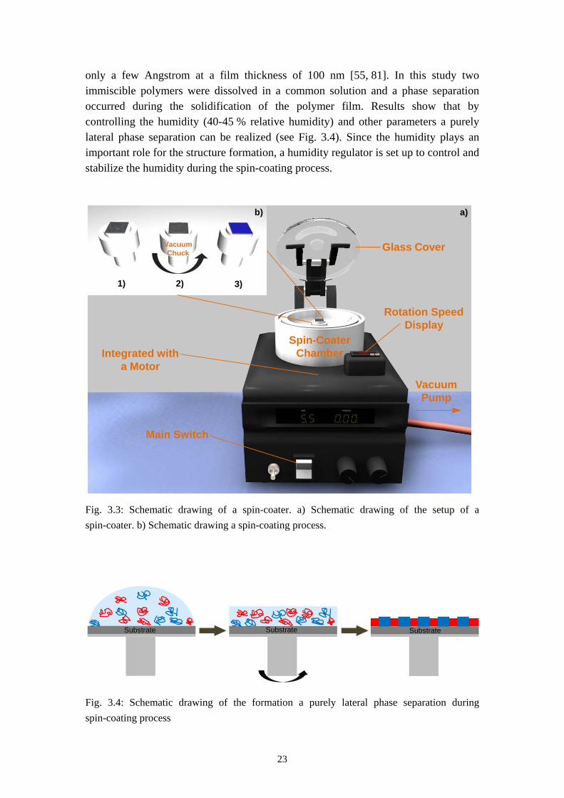
3.1.3 The Humidity-Regulated Spin-Coating Technique
The spin-coating technique is a very common technique in the semiconductor industry to coat a substrate with a thin layer of polymer. As shown in Fig. 3.3a a sample is put on a vacuum chuck which is connected to a vacuum pump and a motor. The substrate is fixed with the vacuum on its back side and can be rotated by the motor. After a droplet of polymer solution is put onto a flat substrate (Fig. 3.3b1), the rotation starts and spreads the liquid over the substrate (Fig. 3.3b2). During the evaporation of the solvent, the polymer solidifies and forms a smooth film (Fig. 3.3b3). The thickness 𝑑 of the resulting film depends on the viscosity and the concentration of the polymer
solution and the spin-frequency 𝑓 (𝑑 ∝ �1 𝑓⁄ ). Film thickness from a few
Angstrom up to a few micrometers can be realized using polymer solutions with concentration between 1 mg/ml and 50 mg/ml and spin rates between 1000 and 10000 rotations per minute (rpm). Polymer films fabricated from solutions of good solvents for the corresponding polymers shows a surprising quality with a roughness of e.g.
23
only a few Angstrom at a film thickness of 100 nm [55, 81]. In this study two immiscible polymers were dissolved in a common solution and a phase separation occurred during the solidification of the polymer film. Results show that by controlling the humidity (40-45 % relative humidity) and other parameters a purely lateral phase separation can be realized (see Fig. 3.4). Since the humidity plays an important role for the structure formation, a humidity regulator is set up to control and stabilize the humidity during the spin-coating process.
Fig. 3.3: Schematic drawing of a spin-coater. a) Schematic drawing of the setup of a spin-coater. b) Schematic drawing a spin-coating process.
Fig. 3.4: Schematic drawing of the formation a purely lateral phase separation during spin-coating process
Vacuum Pump
Glass CoverVacuum Chuck
Spin-CoaterChamber
Main Switch
Rotation SpeedDisplay
a)b)
1) 2) 3)
Integrated with a Motor
Substrate SubstrateSubstrate
24
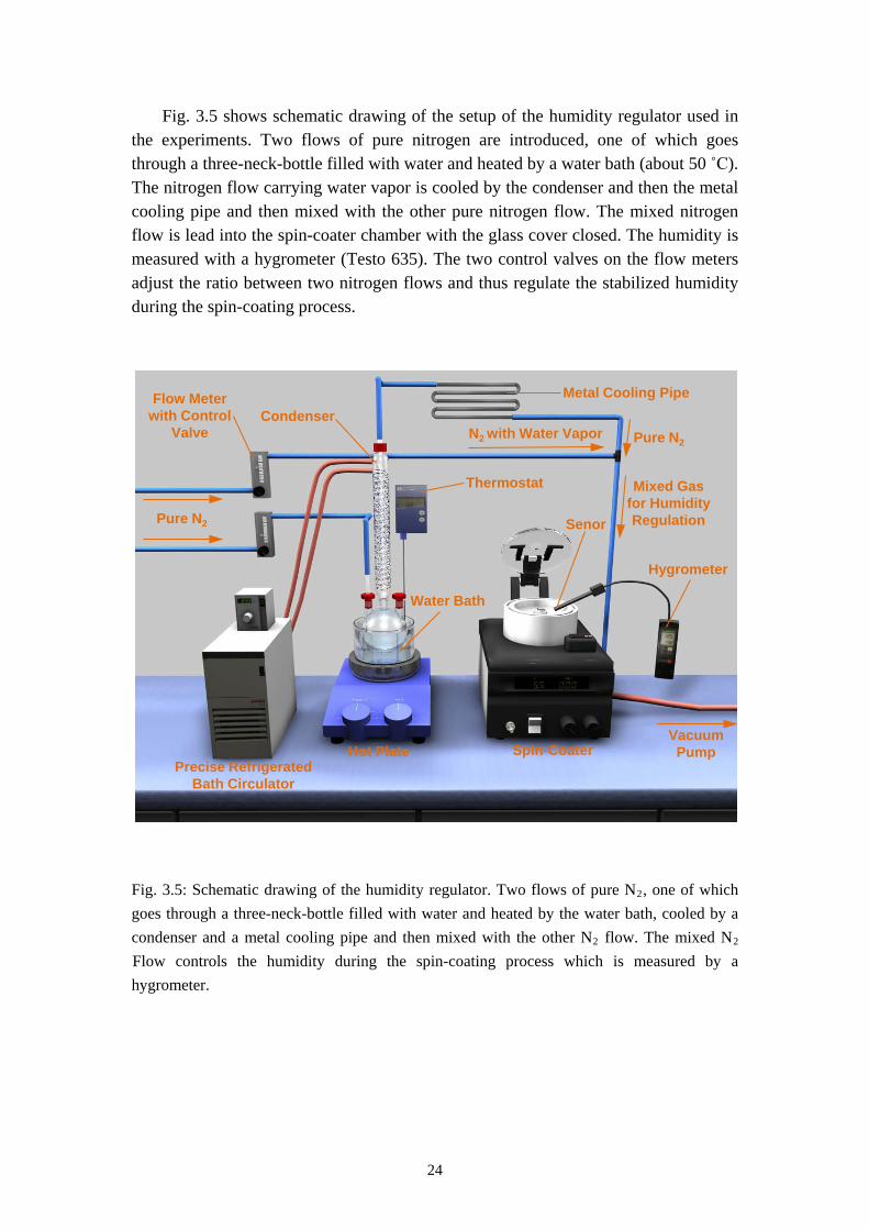
Fig. 3.5 shows schematic drawing of the setup of the humidity regulator used in the experiments. Two flows of pure nitrogen are introduced, one of which goes through a three-neck-bottle filled with water and heated by a water bath (about 50 ˚C). The nitrogen flow carrying water vapor is cooled by the condenser and then the metal cooling pipe and then mixed with the other pure nitrogen flow. The mixed nitrogen flow is lead into the spin-coater chamber with the glass cover closed. The humidity is measured with a hygrometer (Testo 635). The two control valves on the flow meters adjust the ratio between two nitrogen flows and thus regulate the stabilized humidity during the spin-coating process.
Fig. 3.5: Schematic drawing of the humidity regulator. Two flows of pure N2, one of which goes through a three-neck-bottle filled with water and heated by the water bath, cooled by a condenser and a metal cooling pipe and then mixed with the other N2 flow. The mixed N2
Flow controls the humidity during the spin-coating process which is measured by a hygrometer.
Pure N2
Vacuum PumpSpin-Coater
Precise Refrigerated Bath Circulator
Hot Plate
Condenser
Thermostat
Metal Cooling Pipe
Water Bath
Senor
Hygrometer
N2 with Water Vapor Pure N2
Mixed Gas for Humidity Regulation
Flow Meter with Control
Valve
25
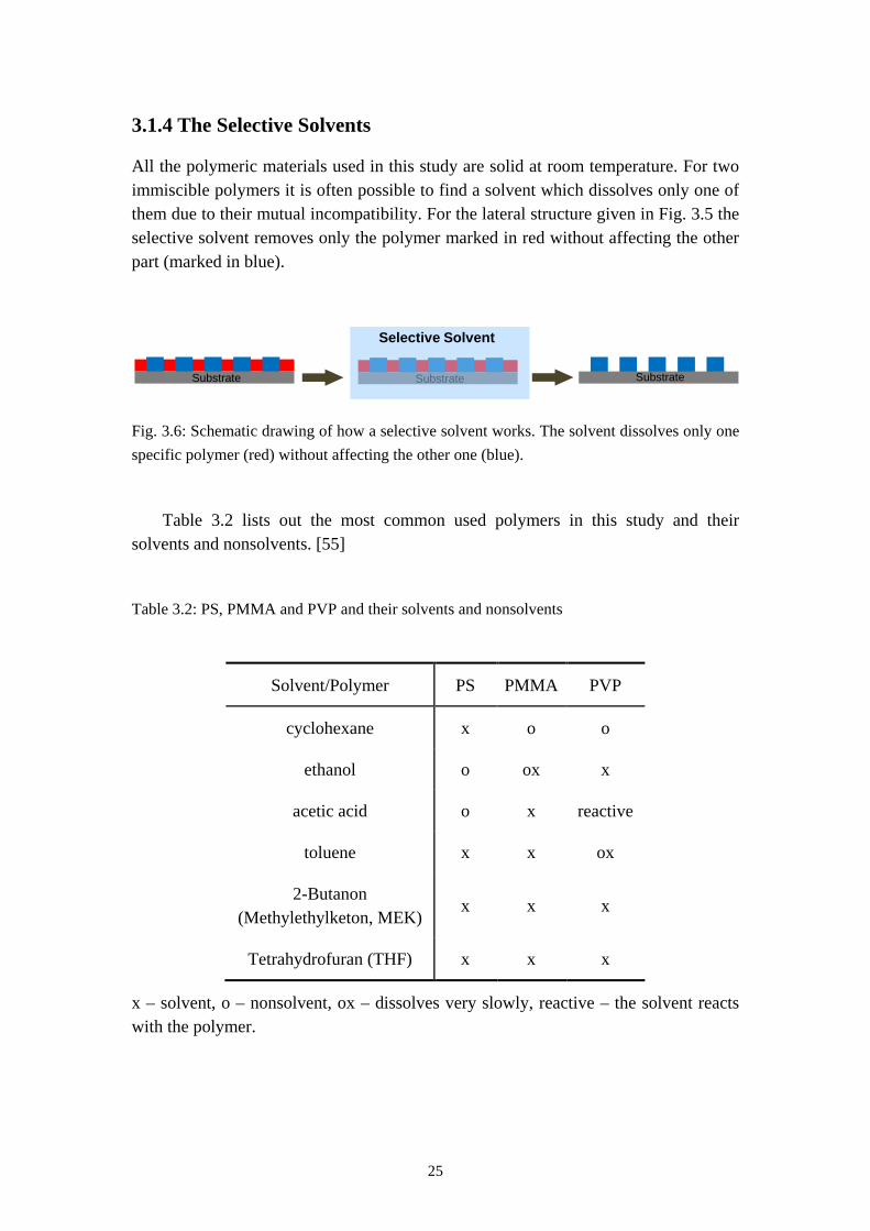
3.1.4 The Selective Solvents
All the polymeric materials used in this study are solid at room temperature. For two immiscible polymers it is often possible to find a solvent which dissolves only one of them due to their mutual incompatibility. For the lateral structure given in Fig. 3.5 the selective solvent removes only the polymer marked in red without affecting the other part (marked in blue).
Fig. 3.6: Schematic drawing of how a selective solvent works. The solvent dissolves only one specific polymer (red) without affecting the other one (blue).
Table 3.2 lists out the most common used polymers in this study and their solvents and nonsolvents. [55]
Table 3.2: PS, PMMA and PVP and their solvents and nonsolvents
Solvent/Polymer PS PMMA PVP
cyclohexane x o o
ethanol o ox x
acetic acid o x reactive
toluene x x ox
2-Butanon (Methylethylketon, MEK)
x x x
Tetrahydrofuran (THF) x x x
x – solvent, o – nonsolvent, ox – dissolves very slowly, reactive – the solvent reacts with the polymer.
SubstrateSubstrate Substrate
Selective Solvent
26
3.2 Metal Film Deposition with Thermal Evaporation Technique
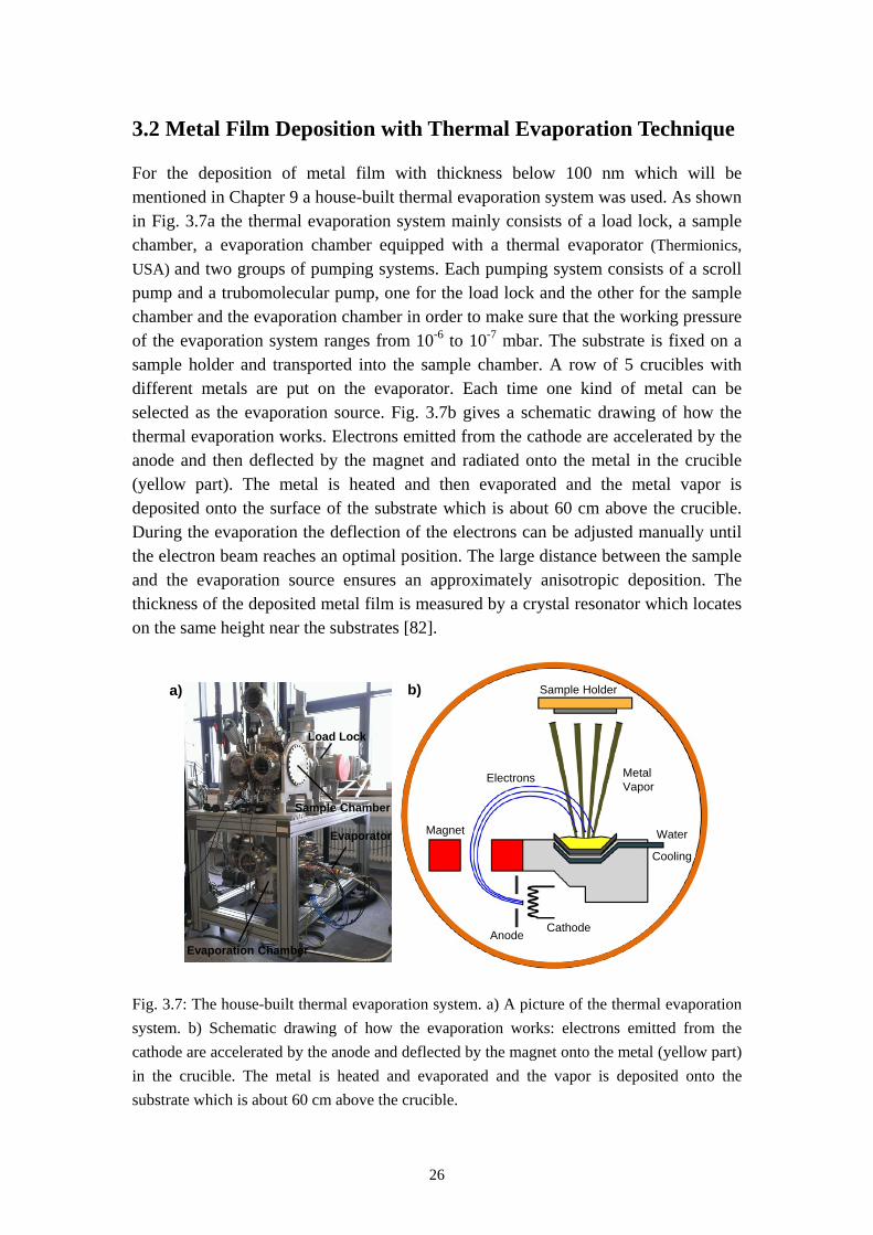
For the deposition of metal film with thickness below 100 nm which will be mentioned in Chapter 9 a house-built thermal evaporation system was used. As shown in Fig. 3.7a the thermal evaporation system mainly consists of a load lock, a sample chamber, a evaporation chamber equipped with a thermal evaporator (Thermionics, USA) and two groups of pumping systems. Each pumping system consists of a scroll pump and a trubomolecular pump, one for the load lock and the other for the sample chamber and the evaporation chamber in order to make sure that the working pressure of the evaporation system ranges from 10-6 to 10-7
mbar. The substrate is fixed on a sample holder and transported into the sample chamber. A row of 5 crucibles with different metals are put on the evaporator. Each time one kind of metal can be selected as the evaporation source. Fig. 3.7b gives a schematic drawing of how the thermal evaporation works. Electrons emitted from the cathode are accelerated by the anode and then deflected by the magnet and radiated onto the metal in the crucible (yellow part). The metal is heated and then evaporated and the metal vapor is deposited onto the surface of the substrate which is about 60 cm above the crucible. During the evaporation the deflection of the electrons can be adjusted manually until the electron beam reaches an optimal position. The large distance between the sample and the evaporation source ensures an approximately anisotropic deposition. The thickness of the deposited metal film is measured by a crystal resonator which locates on the same height near the substrates [82].
Fig. 3.7: The house-built thermal evaporation system. a) A picture of the thermal evaporation system. b) Schematic drawing of how the evaporation works: electrons emitted from the cathode are accelerated by the anode and deflected by the magnet onto the metal (yellow part) in the crucible. The metal is heated and evaporated and the vapor is deposited onto the substrate which is about 60 cm above the crucible.
Magnet
CathodeAnode
Electrons Metal Vapor
Water
Cooling
Sample Holder
Load Lock
Sample Chamber
Evaporation Chamber
Evaporator
a) b)
27
3.3 The Preparation of Silane SAMs in Gas Phase
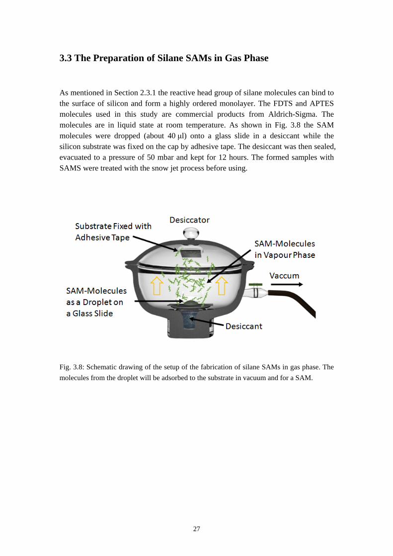
As mentioned in Section 2.3.1 the reactive head group of silane molecules can bind to the surface of silicon and form a highly ordered monolayer. The FDTS and APTES molecules used in this study are commercial products from Aldrich-Sigma. The molecules are in liquid state at room temperature. As shown in Fig. 3.8 the SAM molecules were dropped (about 40 μl) onto a glass slide in a desiccant while the silicon substrate was fixed on the cap by adhesive tape. The desiccant was then sealed, evacuated to a pressure of 50 mbar and kept for 12 hours. The formed samples with SAMS were treated with the snow jet process before using.
Fig. 3.8: Schematic drawing of the setup of the fabrication of silane SAMs in gas phase. The molecules from the droplet will be adsorbed to the substrate in vacuum and for a SAM.
28
3.4 The Preparation of PS Brush
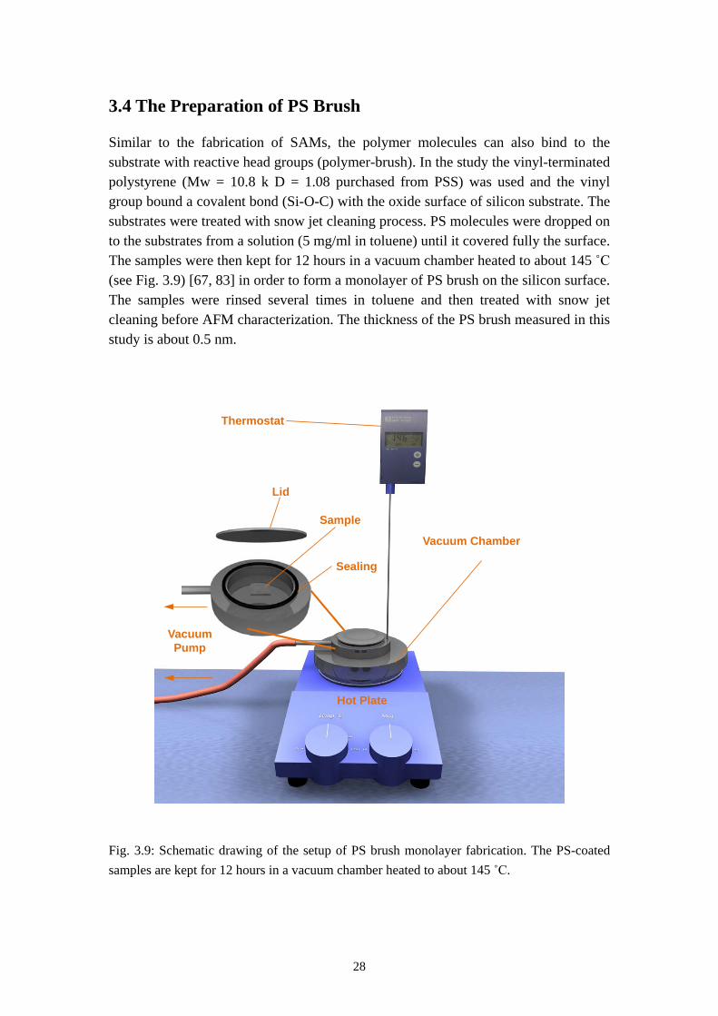
Similar to the fabrication of SAMs, the polymer molecules can also bind to the substrate with reactive head groups (polymer-brush). In the study the vinyl-terminated polystyrene (Mw = 10.8 k D = 1.08 purchased from PSS) was used and the vinyl group bound a covalent bond (Si-O-C) with the oxide surface of silicon substrate. The substrates were treated with snow jet cleaning process. PS molecules were dropped on to the substrates from a solution (5 mg/ml in toluene) until it covered fully the surface. The samples were then kept for 12 hours in a vacuum chamber heated to about 145 ˚C (see Fig. 3.9) [67, 83] in order to form a monolayer of PS brush on the silicon surface. The samples were rinsed several times in toluene and then treated with snow jet cleaning before AFM characterization. The thickness of the PS brush measured in this study is about 0.5 nm.
Fig. 3.9: Schematic drawing of the setup of PS brush monolayer fabrication. The PS-coated samples are kept for 12 hours in a vacuum chamber heated to about 145 ˚C.
Hot Plate
Thermostat
Vacuum Chamber
Vacuum Pump
Lid
Sample
Sealing
29
4. Characterization Methods
4.1 Optical Microscope
Thin polymer films on silicon substrates show beautiful interference colors due to the significant difference in refractive index between the film and the substrate. [84] Different thicknesses can thus be recognized from their colors (shown in Table 4.1), which makes it possible to investigate the thin polymer films with optical microscopy. In the study a Leica DMR (from Leica) was used to observe the lateral structures of the polymer blend system.
Table 4.1: Dependence of the interference color on thickness of polymer film [55]
Thickness (nm) 10 70 100 120 150 200
Color Light Brown Dark Brown Dark Blue Light Blue Yellow Purple
4.2 Scanning Electron Microscope (SEM)
The Scanning Electron Microscope is one of the most versatile instruments available for the examination and analysis of the micro- and nanostructural characteristics of solid objects. It gathers information from the sample by scanning it with a high-energy electron beam in high vacuum. After the primary electron beam hit the sample surface, the electrons are either back-scattered, which will be then called the back-scattered electrons (BSE) or make inelastic interactions with the valance electrons within the surface area. The electrons will be released from the surface if the incident electron has enough energy. These released electrons are called secondary electrons (SE). The BSE and SE are collected by detector or detectors and converted into images demonstrating different information of the sample surface. However, only SEs originating from a very thin surface layer, 5 nm for metal and 50 nm for insulator, can contribute to the detectable signals, as all of the SEs generated in deeper regions of the sample will recombine. The ionized or excited atoms will convert back to their initial stage accompanied by emission of characteristic X-rays or Auger electrons, which provides the possibilities for analytical methods like Energy-Dispersive X-Ray Spectroscopy (EDX) [126].
30
SEM is not a direct imaging instrument like optical microscope and therefore its resolution limit depends not directly on the wavelength of the electron beam but on the size of the interaction area between the primary beam and the sample surface and the grid size and fineness of the electron beam.
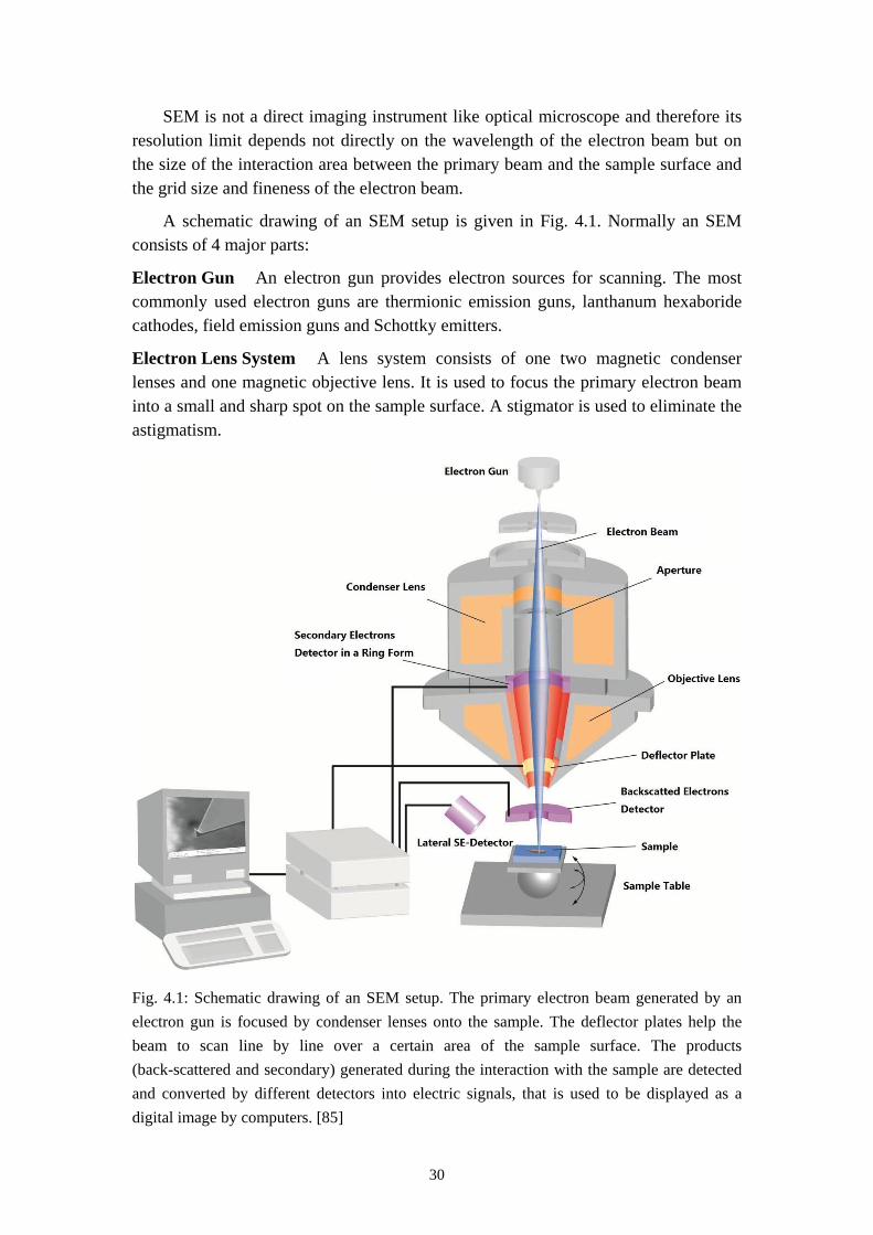
A schematic drawing of an SEM setup is given in Fig. 4.1. Normally an SEM consists of 4 major parts:
Electron Gun An electron gun provides electron sources for scanning. The most commonly used electron guns are thermionic emission guns, lanthanum hexaboride cathodes, field emission guns and Schottky emitters.
Electron Lens System A lens system consists of one two magnetic condenser lenses and one magnetic objective lens. It is used to focus the primary electron beam into a small and sharp spot on the sample surface. A stigmator is used to eliminate the astigmatism.
Fig. 4.1: Schematic drawing of an SEM setup. The primary electron beam generated by an electron gun is focused by condenser lenses onto the sample. The deflector plates help the beam to scan line by line over a certain area of the sample surface. The products (back-scattered and secondary) generated during the interaction with the sample are detected and converted by different detectors into electric signals, that is used to be displayed as a digital image by computers. [85]
31
Deflection System A deflection system deflects the electron beam so that it can scan in a raster fashion over a rectangular area of the sample surface. The magnification is controlled by the degree of deflection which determines the raster width. A smaller raster width means a higher magnification.
Detectors The most commonly used detector is the Everhart-Thornley-Detector which is composed of a scintillator and a photomultiplier. It detects both the secondary electrons and backscattered electrons. The collected signals are amplified, converted and then displayed as a two-dimensional digital image. The brightness of the image depends on the intensity of the SE received by the detector. Edges and steep surfaces tend to be brighter than the flat area as more SEs are emitted in these case. An extra BSE detector can also be put directly above the sample to collect the BSE much more efficiently in order to get a better chemical contrast of the surface. [86,87]
In this study a LEO 1530 was used to characterize the topography of the samples. Low primary electron beam energy (1-5kv) was applied for polymer samples in order to prevent charging effect.
4.3 Atomic Force Microscope
The invention of the Scanning Tunneling Microscope (STM) by Binning, Rohrer and Gerber in 1982 was a mile stone in the development of Scanning Probe Microscopy (SPM). A small tip is used to scan over a surface and sense its conductivity. The current (tunneling current) flows through the tip depends strongly on the distance between the tip and the surface, which makes it possible to image the electric structure of a conductive surface, sometimes even down to atomic resolution. [88]. A few years later (1986) Binning, Gerber and Quate extended the principle of STM to nonconductive surfaces and thus the first Atomic Force Microscope (AFM) was born. A sharp tip mounted on a soft cantilever spring was used to scan the sample surface and the forces between the atoms of the sample surface and the tip were measured to give an image containing 3-dimensional information [89]. It is also possible scan sample surfaces down to atomic resolution [90]. The setup and the functional modes are described in the chapters below.
4.3.1 General Construction of AFM
Fig. 4.1 gives a schematic drawing of an AFM setup. An AFM uses a tip fixed on a cantilever spring which is normally made from silicon or silicon nitride. The typical
32
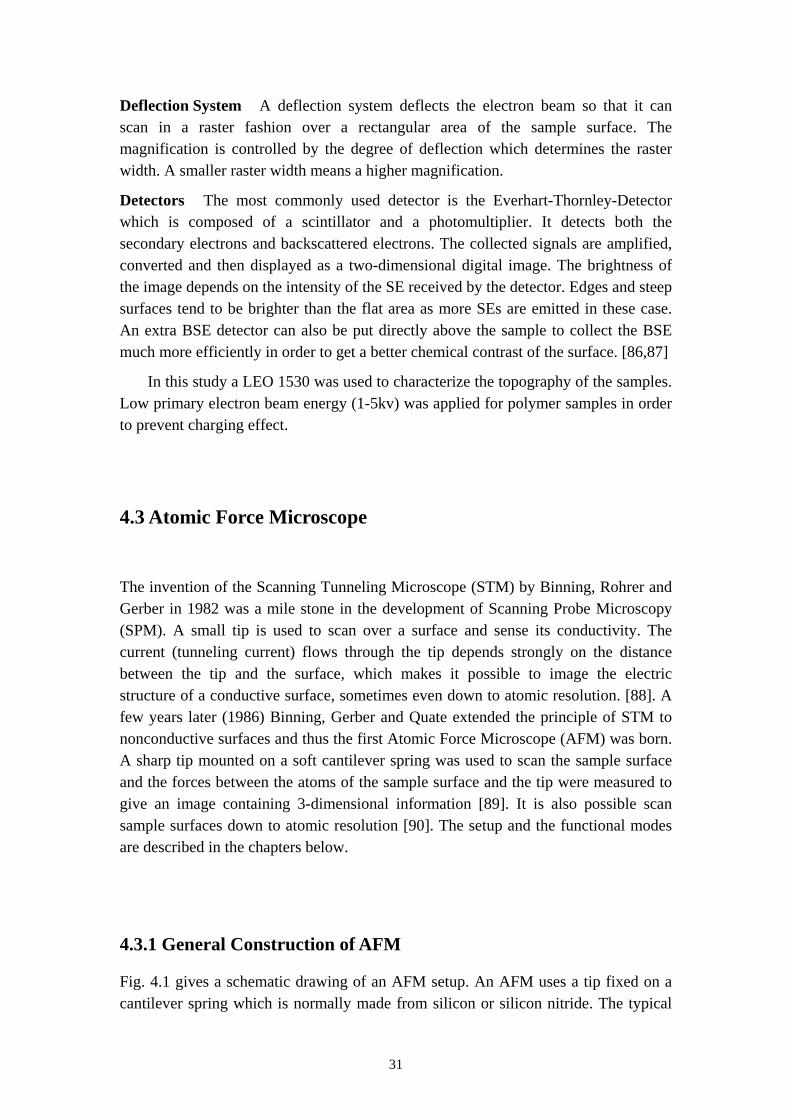
diameter of the sharp end of a normal tip is about 20 nm. The sample is mounted on a piezo scan element. When the tip is brought very close to the sample surface, the interaction between the tip and the sample surface will cause a deflection of the cantilever from its rest position. This deflection will change the reflection angle of a laser which is focused on the back side of the cantilever end and thus detected by the 4-segment photodiode by measuring the vertical and horizontal deviation of the reflected laser beam from the center of the photodiode. In most cases (the multimode AFMS) it is the sample instead of the cantilever which moves for the scan. Therefore the sample is fixed either magnetically or mechanically. The piezo scan element can bend in x- and y-direction and move in z-direction. All the movement is managed by a computer. Nowadays there are also AFMs which put all the electronic parts into the top part, like Bruker ICON, which makes it possible to perform scans on much larger samples e.g. 30 x 30 cm2
.
Fig. 4.2: Schematic drawing of an AFM setup. A laser beam is focused on the back side of the cantilever end. The bending and torsion of the cantilever caused by the interactions between the tip and the surface are detected by the 4-segment photodiode by measuring the deviation of the reflected laser beam from the center. The sample is fixed onto a piezo scan element Controlled by a computer, the piezo scan element can bend in x- and y-direction and move in z-direction to make the approach of the sample to the tip and the scan.
Before the measurement the laser beam must be adjusted so that it hits the cantilever end and reflects onto the photodiode with the maximal intensity. Then the tilt angle of the 4-segment photodiode must be adjusted in order to make sure the laser beam reflects exactly onto the center at the rest position of the cantilever. This can be
4-Segment Photodiode
Laser
Piezo Scan Element
Sample CantileverTip
A B
DC
33
done by eliminate the vertical ((A+B) – (C+D)) and horizontal ((A+C) – (B+D)) intensity differences.
4.3.2 Interactions between Samples and Cantilevers
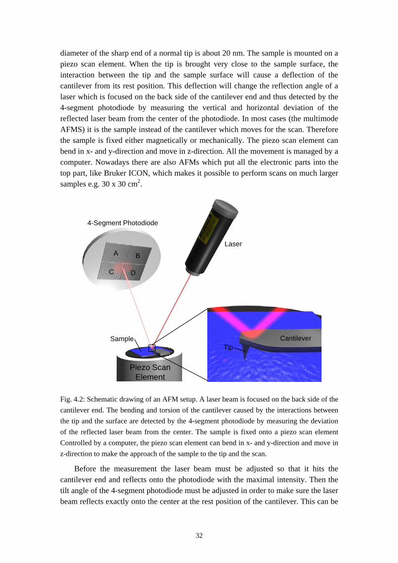
The so-called atomic forces are the many different forces that the tip undergoes when it approaches the sample surface with the cantilever. The atomic forces can be expressed by the Lennard-Jones-Potential 𝜑(𝑟) in a general form as:
𝜑(𝑟) = 4𝜀[�𝜎𝑟�12− �
𝜎𝑟�6
]
where 𝜀 is the depth of the potential well, 𝜎 the finite distance at which the potential is zero and 𝑟 the distance between the sample and the cantilever.
Fig. 4.3: The Lennard-Jones-Potential. The repulsive force is described by the positive 𝑟−12-term e the attractive force described by the negative 𝑟−6-term [67,91]. The brown line indicates the potential range for the contact mode while the yellow line for the tapping mode.
As shown in Fig. 4.3 the 𝑟−12-term describes the repulsive force while the 𝑟−6-term describes the attractive force which in this case mainly refers to van der Waals interaction. For the two most often used AFM modes, the contact mode and the tapping mode the sum of the forces between cantilever and sample is repulsive in contact mode as they are very close while in the tapping mode the van der Waals interaction starts to dominate resulting in a attractive sum of atomic forces [91].
4.1
34
4.3.3 The Contact Mode
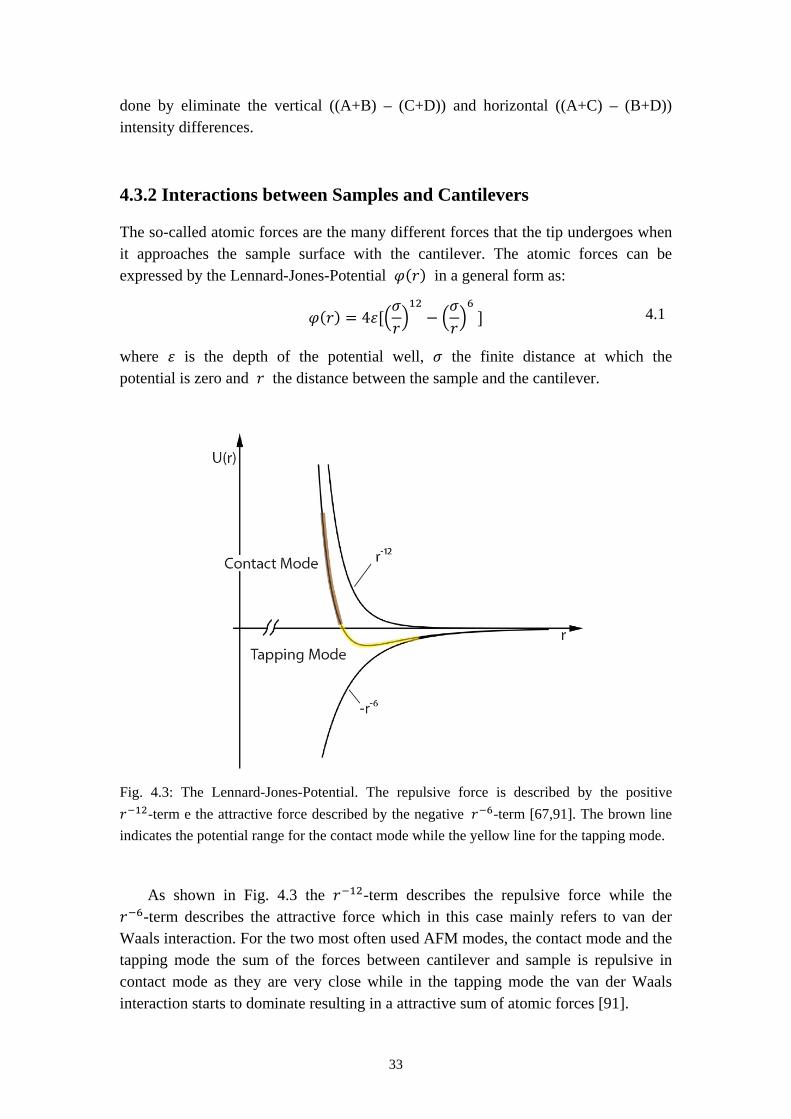
The AFM tip contacts continuously with the sample surface in the contact mode. There are two methods of measurements to drive this mode. One is called constant height mode, which means the distance between the sample and the cantilever is held constant and the deviation on the photodiode from the center caused by bending and torsion of the cantilever is recorded and interpreted into a topographic image of the sample surface. The other one is called constant force mode, which means that the deflection of the cantilever is defined as ‘offset’ and kept constant by moving the sample by the piezo scan element in z-direction. The changes in z-direction can be directly interpreted into a topographic image. The disadvantage of contact mode is very obvious: it might damage the sample surface or the AFM tip as they are in contact.
Fig. 4.4: Schematic drawing of the lateral force mode. The scan direction is perpendicular to the long axis of the cantilever and therefore the lateral force can be measured by the torsion of the cantilever in the scan direction. [92]
In addition to the topographic images, the development of lateral force mode (LFM) provides the possibility to measure the sample with a friction contrast. As shown in Fig. 4.3 when the scan direction is perpendicular to the long axis of the cantilever, a lateral force will cause the torsion of the cantilever due to the friction between the tip and the sample surface. The torsion can be recorded as the lateral intensity difference ((A+C) – (B+D)) by the 4-segment photodiode. The degree torsion depends mainly on the intensity of the friction but it is also influenced by the pressure the tip applied on the surface and also the interactions between them [93, 94]. The friction image can show the chemical contrast of the surface for materials such as polymer or organic self-assembled monolayer [1, 95].
35
4.3.4 The Tapping Mode
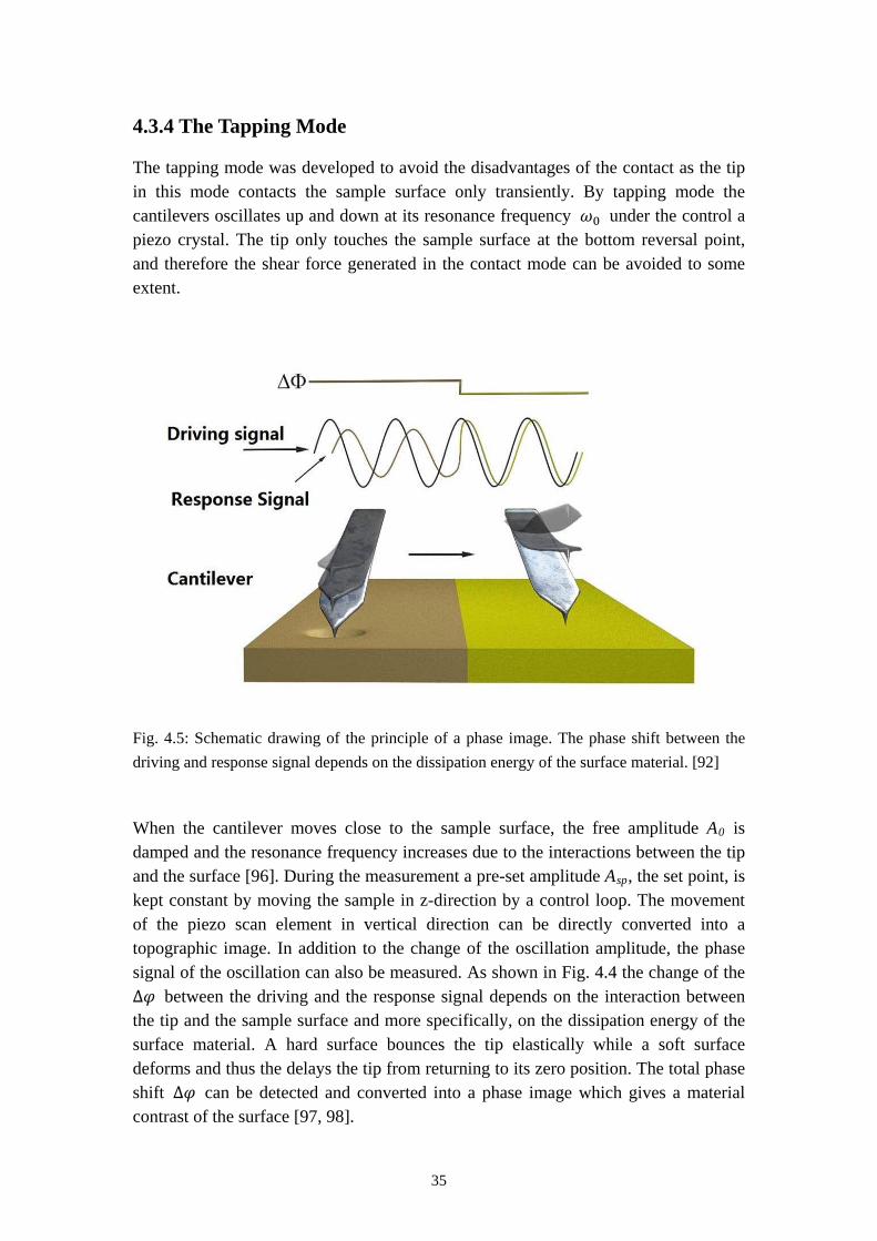
The tapping mode was developed to avoid the disadvantages of the contact as the tip in this mode contacts the sample surface only transiently. By tapping mode the cantilevers oscillates up and down at its resonance frequency 𝜔0 under the control a piezo crystal. The tip only touches the sample surface at the bottom reversal point, and therefore the shear force generated in the contact mode can be avoided to some extent.
Fig. 4.5: Schematic drawing of the principle of a phase image. The phase shift between the driving and response signal depends on the dissipation energy of the surface material. [92]
When the cantilever moves close to the sample surface, the free amplitude A0 is damped and the resonance frequency increases due to the interactions between the tip and the surface [96]. During the measurement a pre-set amplitude Asp, the set point, is kept constant by moving the sample in z-direction by a control loop. The movement of the piezo scan element in vertical direction can be directly converted into a topographic image. In addition to the change of the oscillation amplitude, the phase signal of the oscillation can also be measured. As shown in Fig. 4.4 the change of the ∆𝜑 between the driving and the response signal depends on the interaction between the tip and the sample surface and more specifically, on the dissipation energy of the surface material. A hard surface bounces the tip elastically while a soft surface deforms and thus the delays the tip from returning to its zero position. The total phase shift ∆𝜑 can be detected and converted into a phase image which gives a material contrast of the surface [97, 98].
36
4.3.5 Analysis of Grain Size Distribution.
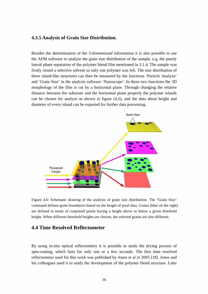
Besides the determination of the 3-dimensional information it is also possible to use the AFM software to analyze the grain size distribution of the sample, e.g. the purely lateral phase separation of the polymer blend film mentioned in 3.1.4. The sample was firstly rinsed a selective solvent so only one polymer was left. The size distribution of these island-like structures can then be measured by the functions ‘Particle Analyze’ and ‘Grain Size’ in the analysis software ‘Nanoscope’. In these two functions the 3D morphology of the film is cut by a horizontal plane. Through changing the relative distance between the substrate and the horizontal plane properly the polymer islands can be chosen for analyze as shown in figure (4.5), and the data about height and diameter of every island can be exported for further data processing.
Figure 4.6: Schematic drawing of the analysis of grain size distribution. The "Grain Size" command defines grain boundaries based on the height of pixel data. Grains (blue on the right) are defined in terms of conjoined pixels having a height above or below a given threshold height. When different threshold heights are chosen, the selected grains are also different.
4.4 Time Resolved Reflectometer
By using in-situ optical reflectometry it is possible to study the drying process of spin-coating, which lasts for only one or a few seconds. The first time resolved reflectometer used for this work was published by Jones et al in 2005 [18]. Jones and his colleagues used it to study the development of the polymer blend structure. Later
37
on time-resolved-reflectometer was used as a very convenient method for the determination of evaporation time of solvents and solutions [29].
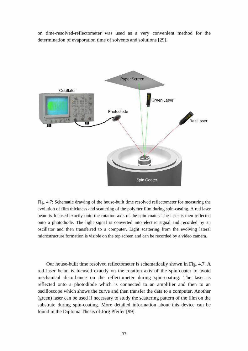
Fig. 4.7: Schematic drawing of the house-built time resolved reflectometer for measuring the evolution of film thickness and scattering of the polymer film during spin-casting. A red laser beam is focused exactly onto the rotation axis of the spin-coater. The laser is then reflected onto a photodiode. The light signal is converted into electric signal and recorded by an oscillator and then transferred to a computer. Light scattering from the evolving lateral microstructure formation is visible on the top screen and can be recorded by a video camera.
Our house-built time resolved reflectometer is schematically shown in Fig. 4.7. A red laser beam is focused exactly on the rotation axis of the spin-coater to avoid mechanical disturbance on the reflectometer during spin-coating. The laser is reflected onto a photodiode which is connected to an amplifier and then to an oscilloscope which shows the curve and then transfer the data to a computer. Another (green) laser can be used if necessary to study the scattering pattern of the film on the substrate during spin-coating. More detailed information about this device can be found in the Diploma Thesis of Jörg Pfeifer [99].
38
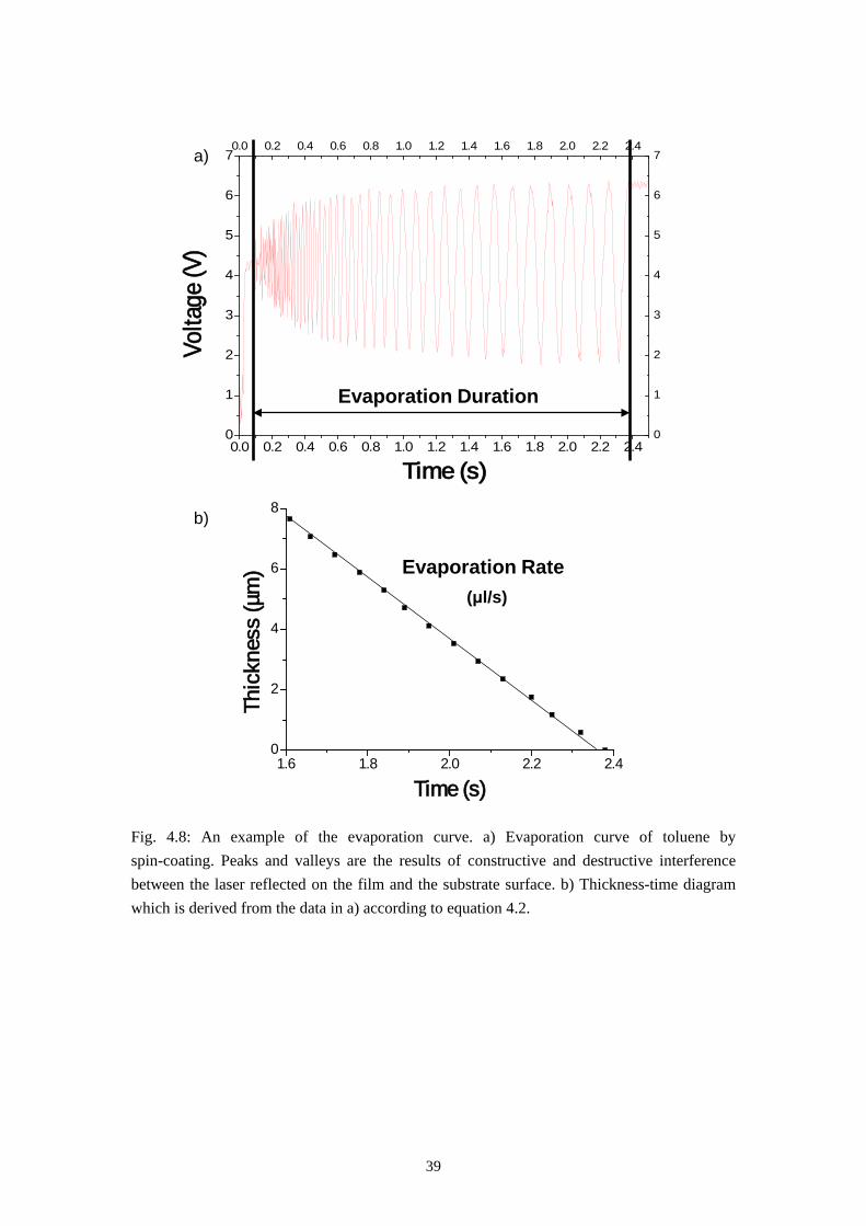
An evaporation curve of toluene is shown in Fig. 4.8a, the peaks and valleys on the curves are the results of constructive and destructive interference between the laser reflected on the film surface and the substrate surface. Each peak or valley represents a specific thickness of the evaporating film, which fulfills the following equation [74]:
𝑑 =
⎩⎪⎨
⎪⎧
𝑚𝜆2𝑛1𝑐𝑜𝑠𝛼′
(2𝑚 + 1)𝜆 2⁄2𝑛1𝑐𝑜𝑠𝛼′
�
while 𝜆 is the wavelength of the laser which is 633 nm, 𝑛1 the refractive index of the film, 𝛼′ the incident angle of the laser on the substrate which can be calculated from the incident angle of the setup and 𝑚 = 0,1,2,3… Therefore, the evaporation curve can be converted into a thickness-time diagram to show directly the evaporation rate of the process (Fig 4.8b).
In this study the time resolved reflectometer was used to investigate the development of the structure of the polymer film in order to give a clearer picture of the formation of the structures. All the curves shown in the dissertation are qualitatively reproducible.
4.1
Constructive interference
Destructive interference
39
Fig. 4.8: An example of the evaporation curve. a) Evaporation curve of toluene by spin-coating. Peaks and valleys are the results of constructive and destructive interference between the laser reflected on the film and the substrate surface. b) Thickness-time diagram which is derived from the data in a) according to equation 4.2.
1.6 1.8 2.0 2.2 2.40
2
4
6
8
Thic
knes
s (µ
m)
Time (s)
Evaporation Rate(μl/s)
0.0 0.2 0.4 0.6 0.8 1.0 1.2 1.4 1.6 1.8 2.0 2.2 2.40
1
2
3
4
5
6
7
Volta
ge (V
)
Time (s)
0.0 0.2 0.4 0.6 0.8 1.0 1.2 1.4 1.6 1.8 2.0 2.2 2.4
0
1
2
3
4
5
6
7
Evaporation Duration
a)
b)
40
4.5 Ellipsometer
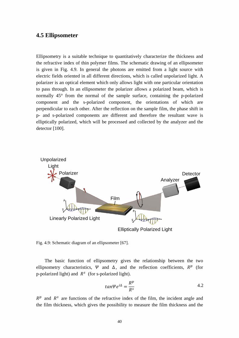
Ellipsometry is a suitable technique to quantitatively characterize the thickness and the refractive index of thin polymer films. The schematic drawing of an ellipsometer is given in Fig. 4.9. In general the photons are emitted from a light source with electric fields oriented in all different directions, which is called unpolarized light. A polarizer is an optical element which only allows light with one particular orientation to pass through. In an ellipsometer the polarizer allows a polarized beam, which is normally 45° from the normal of the sample surface, containing the p-polarized component and the s-polarized component, the orientations of which are perpendicular to each other. After the reflection on the sample film, the phase shift in p- and s-polarized components are different and therefore the resultant wave is elliptically polarized, which will be processed and collected by the analyzer and the detector [100].
Fig. 4.9: Schematic diagram of an ellipsometer [67].
The basic function of ellipsometry gives the relationship between the two ellipsometry characteristics, 𝛹 and ∆ , and the reflection coefficients, 𝑅𝑝 (for p-polarized light) and 𝑅𝑠 (for s-polarized light).
𝑡𝑎𝑛𝛹𝑒𝑖∆ =𝑅𝑝
𝑅𝑠
𝑅𝑝 and 𝑅𝑠 are functions of the refractive index of the film, the incident angle and the film thickness, which gives the possibility to measure the film thickness and the
Unpolarized Light
Polarizer Analyzer
Detector
Film
Linearly Polarized Light
Elliptically Polarized Light
4.2
41
optical properties of specific materials [100]. In this study a commercial M-44 rotating analyzer ellipsometer from J. A. Woollam Co. was used. The ellipsometer is equipped with a Xenon arc lamp source which allows 44 discrete wavelengths between 280 nm and 763 nm. The software of V.A.S.E. for windows (version 3.4.38) from J. A. Woollam Co. was used for data processing.
4.6 Time-of-Flight Secondary Ion Mass Spectrometry
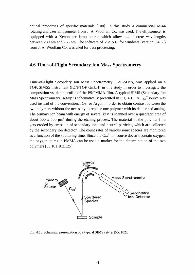
Time-of-Flight Secondary Ion Mass Spectrometry (ToF-SIMS) was applied on a TOF. SIMS5 instrument (ION-TOF GmbH) in this study in order to investigate the composition vs. depth profile of the PS/PMMA film. A typical SIMS (Secondary Ion Mass Spectrometry) set-up is schematically presented in Fig. 4.10. A C60
+ source was used instead of the conventional O2
+ or Argon in order to obtain contrast between the two polymers without the necessity to replace one polymer with its deuterated analog. The primary ion beam with energy of several keV is scanned over a quadratic area of about 500 x 500 μm2 during the etching process. The material of the polymer film gets eroded by emission of secondary ions and neutral particles, which are collected by the secondary ion detector. The count rates of various ionic species are monitored as a function of the sputtering time. Since the C60
+
ion source doesn’t contain oxygen, the oxygen atoms in PMMA can be used a marker for the determination of the two polymers [55,101,102,125].
Fig. 4.10 Schematic presentation of a typical SIMS set-up [55, 102].

42
43
5. Phase Separation in Thin PS/PMMA Film: From
Self-Stratification to Purely Lateral Phase Separation
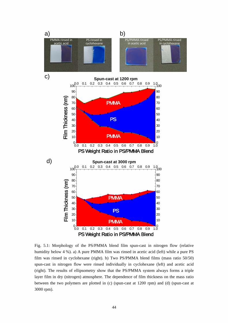
Phase separation between two immiscible polymers ends up normally with a so-called semi-lateral or semi-horizontal morphology via a spin-coating process, which means both horizontal and lateral phase separations occur during spin-casting. In some rare cases self-stratification of polymer blend into a double layer film has also been reported [3, 23]. Models have also been proposed to explain how the lateral structures are formed via a transient double layer film [11, 17, 18, 22, 55, 56]. It will be introduced in this chapter that the system PS/PMMA/MEK forms a triple layer film via self-stratification in dry environment and a purely lateral phase separation (named by us as the Swiss Cheese Structure) when spun-cast at appropriate humidity. Models will also be established to explain the formation of these morphologies.
5.1 Self Stratification of PS/PMMA in Nitrogen Environment
The first result, the self-stratification of PS/PMMA system, is found when a polymer blend solution of PS and PMMA in MEK is spun-cast at very low relative humidity (below 4 %). This was achieved by a nitrogen flow in the spin coater chamber during the coating process. Fig. 5.1a and 5.1b gives the results of rinsing tests of the polymer blend film and homopolymer film spun-cast in nitrogen flow. These films were formed under the conditions listed below:
Relative humidity during spin-casting: <4 %
Rotation speed for spin-casting: 1500 rpm
Concentration of PS and PMMA in MEK (blend solution): 15 mg/ml
Concentration of homopolymer in MEK: 15 mg/ml
Molecular weight of PS: 96 kg/mol
Molecular weight of PMMA: 9.56 kg/mol
PS/PMMA mass ratio in polymer blend solution: 50/50.
44
Fig. 5.1: Morphology of the PS/PMMA blend film spun-cast in nitrogen flow (relative humidity below 4 %). a) A pure PMMA film was rinsed in acetic acid (left) while a pure PS film was rinsed in cyclohexane (right). b) Two PS/PMMA blend films (mass ratio 50/50) spun-cast in nitrogen flow were rinsed individually in cyclohexane (left) and acetic acid (right). The results of ellipsometry show that the PS/PMMA system always forms a triple layer film in dry (nitrogen) atmosphere. The dependence of film thickness on the mass ratio between the two polymers are plotted in (c) (spun-cast at 1200 rpm) and (d) (spun-cast at 3000 rpm).
a) b)
0.0 0.1 0.2 0.3 0.4 0.5 0.6 0.7 0.8 0.9 1.00
10
20
30
40
50
60
70
80
90
100
PS
PMMAFilm
Thi
ckne
ss (n
m)
PS Weight Ratio in PS/PMMA Blend
PMMA
0.0 0.1 0.2 0.3 0.4 0.5 0.6 0.7 0.8 0.9 1.0
0
10
20
30
40
50
60
70
80
90
100
Spun-cast at 1200 rpmc)
0.0 0.1 0.2 0.3 0.4 0.5 0.6 0.7 0.8 0.9 1.00
10
20
30
40
50
60
70
80
90
100
Film
Thi
ckne
ss (n
m)
PS Weight Ratio in PS/PMMA Blend
0.0 0.1 0.2 0.3 0.4 0.5 0.6 0.7 0.8 0.9 1.0
0
10
20
30
40
50
60
70
80
90
100
PMMA
PMMA
PS
Spun-cast at 3000 rpmd)
PMMA rinsed in acetic acid
PS rinsed in cyclohexane
PS/PMMA rinsed in acetic acid
PS/PMMA rinsed in cyclohexane
45
All of the films show colored patterns on the surface since the MEK is not a very good solvent for PMMA and even worse for PS. Polymers dissolved in bad solution forms waviness when spun-cast into a film. This waviness often induces additional lateral structures in polymer blend films and can even dominate the structure formation process. These additional lateral structures are called by us λ2
The homopolymer film of PMMA was rinsed in acetic acid (see Fig. 5.1a left) for one second while the film of PS in cyclohexane (see Fig. 5.1b right). The images taken by digital camera show the majorities of the films were dissolved in both cases. The acetic acid shows a very good solubility to PMMA and leaves no observable rest of PMMA by eyes. The silicon surface freed by cyclohexane looks still very rough due to the rest of PS film fragments. The polymer blend films were rinsed separately in cyclohexane (see Fig. 5.1b left) and acetic acid (see Fig. 6.1b right) for one second and then dried by nitrogen flow. The digital camera images show that no observable change of the film thickness can be found after the rinsing in cyclohexane while the interference color of the film changes from blue/dark brown to light brown. The film with cracks on the left part of the substrate in Fig. 5.1b looks like a film which is floated on the surface of a liquid and then “fished” onto the substrate. Due to the high solubility of acetic acid to PMMA and the high polarity of the acetic acid molecule we make the hypothesis that the polymer blend film formed in dry atmosphere has a PMMA/PS/PMMA triple layer structure. When the film was rinsed in cyclohexane, the solvent didn’t dissolve the PMMA layer on the top and the only access to PS layer in the middle had a thickness below 100 nm. Therefore, no thickness change of the film could be recognized. When rinsed in acetic acid, the top layer of PMMA was dissolved. At the same time the acetic acid molecules wetted the surface of silicon and then dissolved the bottom layer of PMMA as well. Consequently the PS layer in the middle was lifted and then laid back onto the silicon wafer after the film was dried by nitrogen flow.
and were described in earlier works [55, 99].
In order to confirm the hypothesis, the samples were characterized by ellipsometry. Polymer films with different PS/PMMA weight ratio (0/100, 10/90, 20/80, 30/70, 40/60, 50/50, 60/40, 70/30, 80/20, 90/10 and 100/0) were spun-cast at two different rotational speeds (1200 rpm and 3000 rpm) under nitrogen flow (relative humidity below 4 %). The optical parameters of both homopolymers were measured by a white light ellipsometer from a spun-cast film on silicon substrate. Then a multilayer model was established in the software of WVASE32 (Version 3.438), which was used to fit the experimental curves measured from the polymer blend film. The results of fitting with a triple layer model (PMMA/PS/PMMA, bottom to top from left to right) were plotted against the weight ratio of PS in the polymer blend (see Fig. 5.1c-d). The system errors of fitting for all results are less than ±1.0 nm. The total thickness of the polymer film is about 90 nm at 1200 rpm and about 60 nm at 300 rpm. The diagrams at both rotational speeds show that the PS/PMMA blend forms always a triple layer independent of the mass ratio between the two polymers
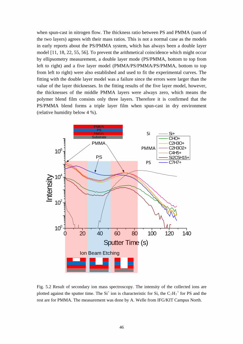
46
when spun-cast in nitrogen flow. The thickness ratio between PS and PMMA (sum of the two layers) agrees with their mass ratios. This is not a normal case as the models in early reports about the PS/PMMA system, which has always been a double layer model [11, 18, 22, 55, 56]. To prevent the arithmetical coincidence which might occur by ellipsometry measurement, a double layer mode (PS/PMMA, bottom to top from left to right) and a five layer model (PMMA/PS/PMMA/PS/PMMA, bottom to top from left to right) were also established and used to fit the experimental curves. The fitting with the double layer model was a failure since the errors were larger than the value of the layer thicknesses. In the fitting results of the five layer model, however, the thicknesses of the middle PMMA layers were always zero, which means the polymer blend film consists only three layers. Therefore it is confirmed that the PS/PMMA blend forms a triple layer film when spun-cast in dry environment (relative humidity below 4 %).
Fig. 5.2 Result of secondary ion mass spectroscopy. The intensity of the collected ions are plotted against the sputter time. The Si+ ion is characteristic for Si, the C7H7
+
0 20 40 60 80 100 120 140100
102
104
106
Inte
nsity
Sputter Time (s)
Si+ CHO+ C2H3O+ C2H3O2+ C4H5+ Si2C5H15+ C7H7+
PMMA
PS
Si
PMMA
PS
Substrate
PSPMMA
PMMA
Ion Beam Etching
for PS and the rest are for PMMA. The measurement was done by A. Welle from IFG/KIT Campus North.
47
In addition, the triple layer film was also analyzed by Secondary Ion Mass Spectrometry (SIMS) with C60 primary ion beam and the result is shown in Fig. 5.2. The collected positively charged secondary ions are analyzed in order to check the composition-depth profile. Since the primary ion source contain only carbon atoms, the oxygen in can be used as a PMMA tracer. In the diagram the intensities of the collected ions are plotted against the sputter time. The Si+ ion is characteristic for Si, the C7H7
+
Finally the surface of each layer was scanned layer by layer by AFM in tapping mode and the retrace images are shown in Fig. 5.3. The SEM images of the PS layer and the bottom PMMA layer are given in Fig. 5.4. The PMMA layer on the top of the film shows a flat surface with roughness in the range of several nanometers (see Fig. 5.3a, b). After the sample was rinsed in acetic acid (3 times, each 10 seconds and dried in the air without nitrogen blow), the PS layer was scanned and the retrace image is shown in Fig. 5.3d. From the cross section profile and the SEM image (see Fig. 5.4a) it is able to observe that the diameter of the holes ranges from 20 to100 nm and the depth is about 20 nm (see Fig. 5.3e). Since acetic acid is a good solvent for PMMA, some solvent molecules will penetrate the holes and dissolve partially the bottom PMMA layer (see Fig. 5.3f). The sample was then rinsed in cyclohexane (3 times, each 10 seconds and dried in the air without nitrogen blow) and the AFM retrace image of the bottom PMMA layer is shown in Fig. 5.3g and the SEM image is shown in Fig. 5.4b. The holes are formed by the rinsing and acetic acid and have diameters ranging from 100 to 200 nm and depth round 15 nm (see Fig. 5.3h, I, Fig. 5.4b). The low contrast of the holes in SEM image gives also evidence that the holes are not deep enough to reach the substrate. Therefore the results point out that the PS/PMMA/MEK system forms a triple layer with lots of PMMA tunnels in the PS layer when spun-cast in dry environment (relative humidity below 4 %).
for PS and the rest are for PMMA. It can be seen very clearly that the PMMA had its maximal amount at the beginning when the etching started, then it decreased and increased again at the next peak. This intensity-depth profile supports strongly the triple layer PMMA/PS/PMMA model. The peak of PS, however, doesn’t appear at the minimum of PMMA. This can be explained by the fact that polystyrene starts cross-linking when exposed to radiation and thus changes the composition of the emitted secondary ions [127]. Therefore together with the results of rinsing experiments shown in Fig. 5.1b and ellipsometry shown in Fig. 5.1c and Fig. 5.1d it is confirmed that the PS/PMMA blend forms a triple layer film when spun-cast in dry environment (relative humidity below 4 %).
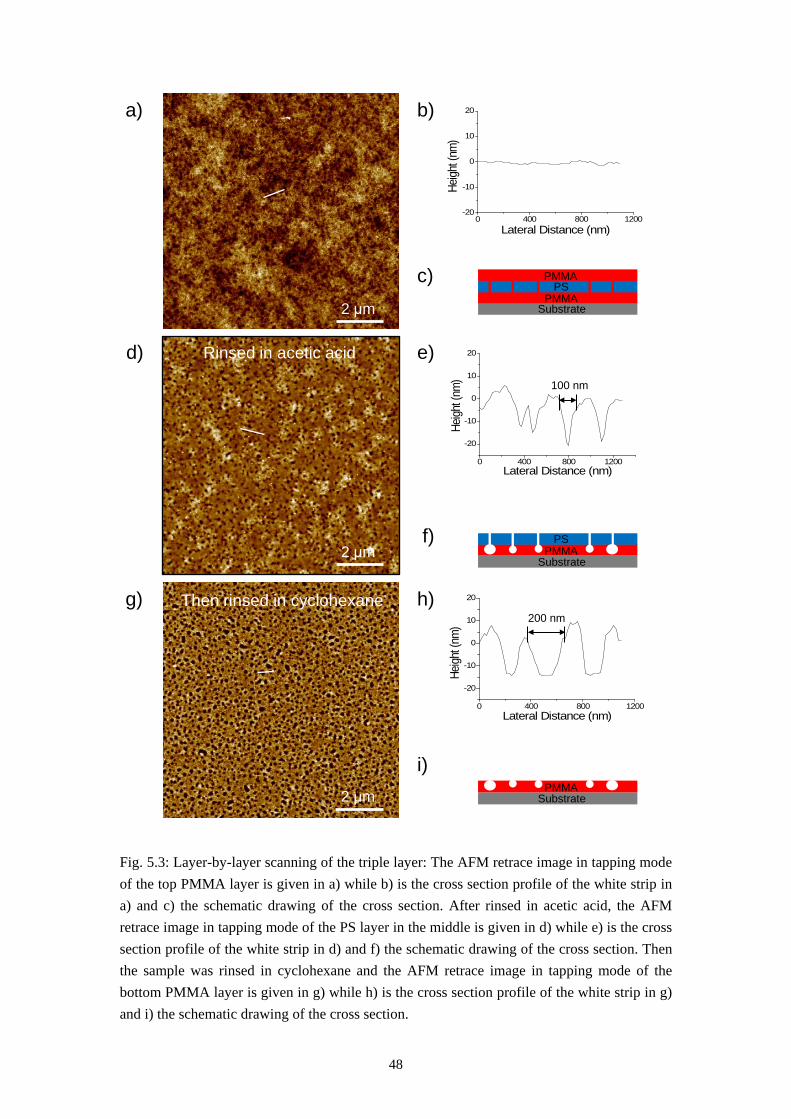
48
Fig. 5.3: Layer-by-layer scanning of the triple layer: The AFM retrace image in tapping mode of the top PMMA layer is given in a) while b) is the cross section profile of the white strip in a) and c) the schematic drawing of the cross section. After rinsed in acetic acid, the AFM retrace image in tapping mode of the PS layer in the middle is given in d) while e) is the cross section profile of the white strip in d) and f) the schematic drawing of the cross section. Then the sample was rinsed in cyclohexane and the AFM retrace image in tapping mode of the bottom PMMA layer is given in g) while h) is the cross section profile of the white strip in g) and i) the schematic drawing of the cross section.
2 μm
2 μm
2 μm
0 400 800 1200
-20
-10
0
10
20
Heigh
t (nm
)Lateral Distance (nm)
0 400 800 1200
-20
-10
0
10
20
Heigh
t (nm
)
Lateral Distance (nm)
SubstratePMMA
PMMAPS
SubstratePMMA
PS
SubstratePMMA
a) b)
d)
c)
f)
e)
g) h)
i)
Rinsed in acetic acid
Then rinsed in cyclohexane
0 400 800 1200-20
-10
0
10
20
Heigh
t (nm
)
Lateral Distance (nm)
100 nm
200 nm
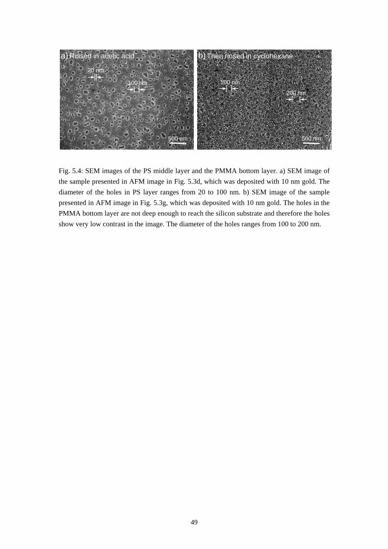
49
Fig. 5.4: SEM images of the PS middle layer and the PMMA bottom layer. a) SEM image of the sample presented in AFM image in Fig. 5.3d, which was deposited with 10 nm gold. The diameter of the holes in PS layer ranges from 20 to 100 nm. b) SEM image of the sample presented in AFM image in Fig. 5.3g, which was deposited with 10 nm gold. The holes in the PMMA bottom layer are not deep enough to reach the silicon substrate and therefore the holes show very low contrast in the image. The diameter of the holes ranges from 100 to 200 nm.
500 nm500 nm
100 nm
20 nm
100 nm
200 nm
Rinsed in acetic acid Then rinsed in cyclohexanea) b)

50
51
5.2 Dependence of Morphology on Spin-Casting Humidity
The morphologies of the polymer blend films are strongly dependent on the humidity of the environment during the spin-casting process. In the following investigation a series of homopolymers (PS and PMMA) and polymer blend films were fabricated under relative humidity ranging from below 4 % to 60 %. The other parameters were set as below:
Rotation speed for spin-casting: 1500 rpm
Solvent for homopolymer and polymer blend: MEK
Concentration of PS and PMMA (blend solution): 15 mg/ml
Concentration of PMMA: 10.5 mg/ml
Concentration of PS: 4.5 mg/ml
Molecular weight of PS: 96 kg/mol
Molecular weight of PMMA: 9.56 kg/mol
PS/PMMA mass ratio in polymer blend solution: 30/70.
The concentrations of the homopolymer solutions were set exactly as the amount of the fractions as they are in the polymer blend solution. The retrace AFM images of these films in tapping mode are listed in Fig. 6.2, which gives a general picture of how the morphologies of the homopolymer and polymer blend films change with the relative humidity during spin-casting. The polymer blend, pure PMMA and the pure PS all form a flat film when spun-cast in the nitrogen flow (relative humidity below 4 %) with a root mean square (rms) roughness of about 0.3 nm (see Fig. 5.5.1a-f). With the increase of the relative humidity, the three different films show different changes in their morphologies.
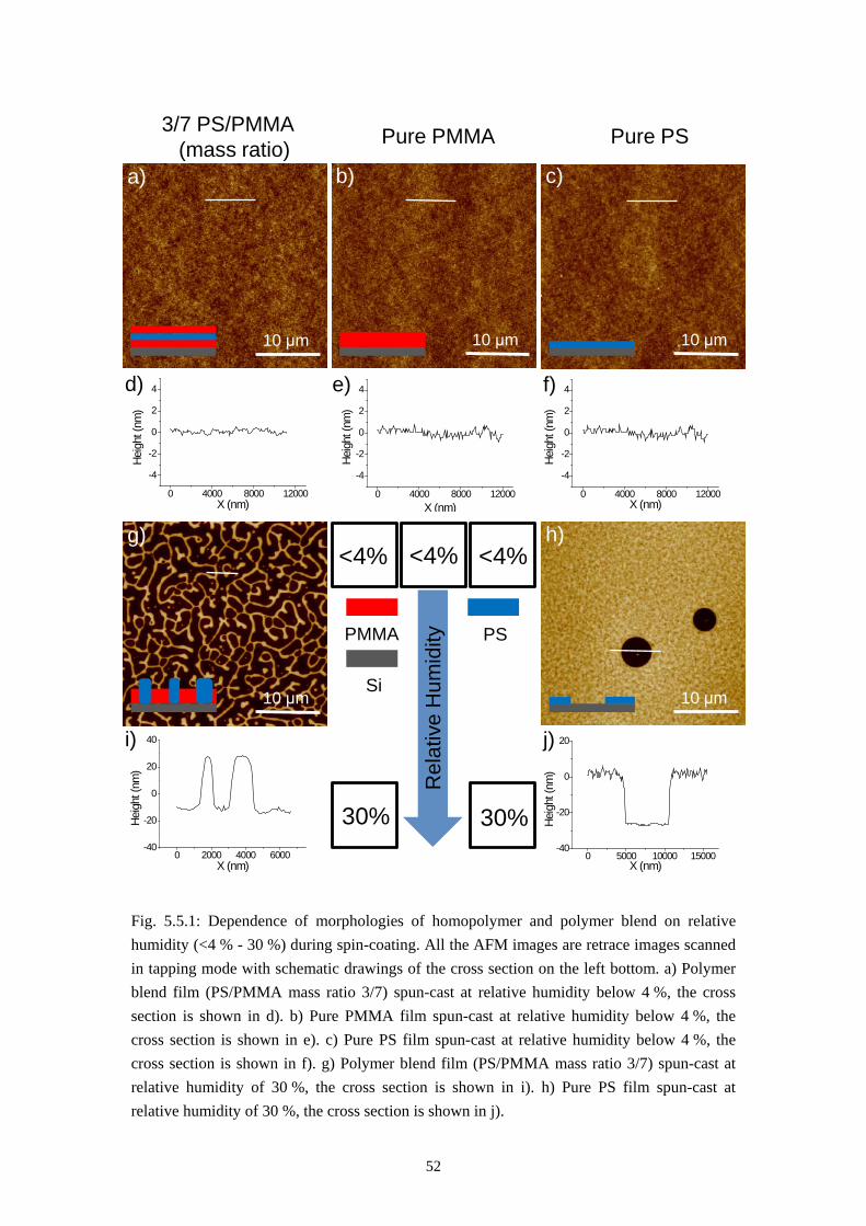
52
Fig. 5.5.1: Dependence of morphologies of homopolymer and polymer blend on relative humidity (<4 % - 30 %) during spin-coating. All the AFM images are retrace images scanned in tapping mode with schematic drawings of the cross section on the left bottom. a) Polymer blend film (PS/PMMA mass ratio 3/7) spun-cast at relative humidity below 4 %, the cross section is shown in d). b) Pure PMMA film spun-cast at relative humidity below 4 %, the cross section is shown in e). c) Pure PS film spun-cast at relative humidity below 4 %, the cross section is shown in f). g) Polymer blend film (PS/PMMA mass ratio 3/7) spun-cast at relative humidity of 30 %, the cross section is shown in i). h) Pure PS film spun-cast at relative humidity of 30 %, the cross section is shown in j).
3/7 PS/PMMA (mass ratio) Pure PMMA Pure PS
10 μm
10 μm
10 μm 10 μm
10 μm
<4% <4% <4%
30% 30%
Rel
ativ
e H
umid
ity
0 4000 8000 12000
-4
-2
0
2
4
Heig
ht (n
m)
X (nm)
0 2000 4000 6000-40
-20
0
20
40
Heig
ht (n
m)
X (nm)
0 4000 8000 12000
-4
-2
0
2
4
Heig
ht (n
m)
X (nm)0 4000 8000 12000
-4
-2
0
2
4
Heig
ht (n
m)
X (nm)
0 5000 10000 15000-40
-20
0
20
Heig
ht (n
m)
X (nm)
a) b) c)
d) e) f)
g) h)
i) j)
PMMA PS
Si
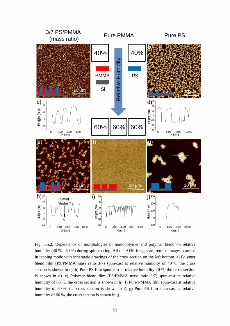
53
Fig. 5.5.2: Dependence of morphologies of homopolymer and polymer blend on relative humidity (40 % - 60 %) during spin-coating. All the AFM images are retrace images scanned in tapping mode with schematic drawings of the cross section on the left bottom. a) Polymer blend film (PS/PMMA mass ratio 3/7) spun-cast at relative humidity of 40 %, the cross section is shown in c). b) Pure PS film spun-cast at relative humidity 40 %, the cross section is shown in d). e) Polymer blend film (PS/PMMA mass ratio 3/7) spun-cast at relative humidity of 60 %, the cross section is shown in h). f) Pure PMMA film spun-cast at relative humidity of 60 %, the cross section is shown in i). g) Pure PS film spun-cast at relative humidity of 60 %, the cross section is shown in j).
10 μm
10 μm 10 μm
10 μm
10 μm
40% 40%
60%60%60%0 1000 2000 3000
-20
0
20
40
Heig
ht (n
m)
X (nm)
0 2000 4000 6000 8000-100
-50
0
50
100
150
Heig
ht (n
m)
X (nm)0 2000 4000 6000 8000
-15
-10
-5
0
5
10
Heig
ht (n
m)
X (nm)
Rel
ativ
e H
umid
ity
0 4000 8000 12000-60
-40
-20
0
20
40
60
Heig
ht (n
m)
X (nm)
0 4000 8000 12000-100
0
100
200
300
Heig
ht (n
m)
X (nm)
3/7 PS/PMMA (mass ratio) Pure PMMA Pure PS
a)
f)
b)
c)
i)
d)
e) g)
h) j)
PMMA PS
Si
Small holes
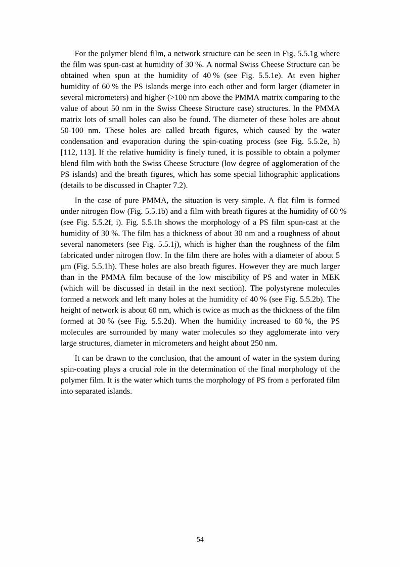
54
For the polymer blend film, a network structure can be seen in Fig. 5.5.1g where the film was spun-cast at humidity of 30 %. A normal Swiss Cheese Structure can be obtained when spun at the humidity of 40 % (see Fig. 5.5.1e). At even higher humidity of 60 % the PS islands merge into each other and form larger (diameter in several micrometers) and higher (>100 nm above the PMMA matrix comparing to the value of about 50 nm in the Swiss Cheese Structure case) structures. In the PMMA matrix lots of small holes can also be found. The diameter of these holes are about 50-100 nm. These holes are called breath figures, which caused by the water condensation and evaporation during the spin-coating process (see Fig. 5.5.2e, h) [112, 113]. If the relative humidity is finely tuned, it is possible to obtain a polymer blend film with both the Swiss Cheese Structure (low degree of agglomeration of the PS islands) and the breath figures, which has some special lithographic applications (details to be discussed in Chapter 7.2).
In the case of pure PMMA, the situation is very simple. A flat film is formed under nitrogen flow (Fig. 5.5.1b) and a film with breath figures at the humidity of 60 % (see Fig. 5.5.2f, i). Fig. 5.5.1h shows the morphology of a PS film spun-cast at the humidity of 30 %. The film has a thickness of about 30 nm and a roughness of about several nanometers (see Fig. 5.5.1j), which is higher than the roughness of the film fabricated under nitrogen flow. In the film there are holes with a diameter of about 5 μm (Fig. 5.5.1h). These holes are also breath figures. However they are much larger than in the PMMA film because of the low miscibility of PS and water in MEK (which will be discussed in detail in the next section). The polystyrene molecules formed a network and left many holes at the humidity of 40 % (see Fig. 5.5.2b). The height of network is about 60 nm, which is twice as much as the thickness of the film formed at 30 % (see Fig. 5.5.2d). When the humidity increased to 60 %, the PS molecules are surrounded by many water molecules so they agglomerate into very large structures, diameter in micrometers and height about 250 nm.
It can be drawn to the conclusion, that the amount of water in the system during spin-coating plays a crucial role in the determination of the final morphology of the polymer film. It is the water which turns the morphology of PS from a perforated film into separated islands.
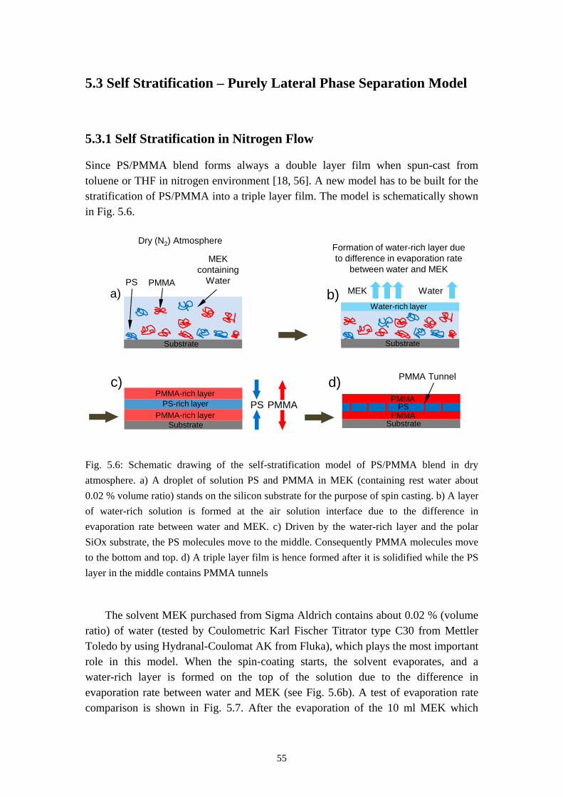
55
5.3 Self Stratification – Purely Lateral Phase Separation Model
5.3.1 Self Stratification in Nitrogen Flow
Since PS/PMMA blend forms always a double layer film when spun-cast from toluene or THF in nitrogen environment [18, 56]. A new model has to be built for the stratification of PS/PMMA into a triple layer film. The model is schematically shown in Fig. 5.6.
Fig. 5.6: Schematic drawing of the self-stratification model of PS/PMMA blend in dry atmosphere. a) A droplet of solution PS and PMMA in MEK (containing rest water about 0.02 % volume ratio) stands on the silicon substrate for the purpose of spin casting. b) A layer of water-rich solution is formed at the air solution interface due to the difference in evaporation rate between water and MEK. c) Driven by the water-rich layer and the polar SiOx substrate, the PS molecules move to the middle. Consequently PMMA molecules move to the bottom and top. d) A triple layer film is hence formed after it is solidified while the PS layer in the middle contains PMMA tunnels
The solvent MEK purchased from Sigma Aldrich contains about 0.02 % (volume ratio) of water (tested by Coulometric Karl Fischer Titrator type C30 from Mettler Toledo by using Hydranal-Coulomat AK from Fluka), which plays the most important role in this model. When the spin-coating starts, the solvent evaporates, and a water-rich layer is formed on the top of the solution due to the difference in evaporation rate between water and MEK (see Fig. 5.6b). A test of evaporation rate comparison is shown in Fig. 5.7. After the evaporation of the 10 ml MEK which
Substrate
PS PMMA
MEK containing
Watera)
Substrate
MEK Water
Water-rich layerb)
SubstratePMMA-rich layer
PMMA-rich layerPS-rich layer PS PMMA
c)
Formation of water-rich layer due to difference in evaporation rate
between water and MEK
SubstratePMMA
PMMAPS
d) PMMA Tunnel
Dry (N2) Atmosphere
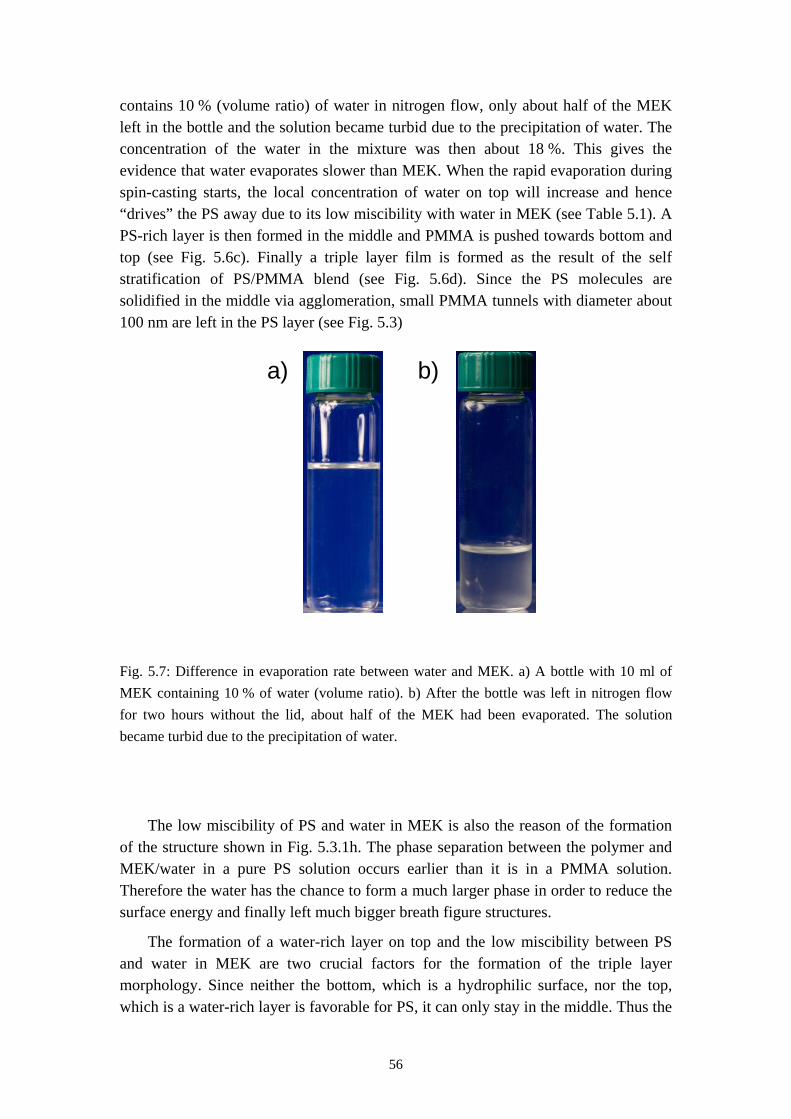
56
contains 10 % (volume ratio) of water in nitrogen flow, only about half of the MEK left in the bottle and the solution became turbid due to the precipitation of water. The concentration of the water in the mixture was then about 18 %. This gives the evidence that water evaporates slower than MEK. When the rapid evaporation during spin-casting starts, the local concentration of water on top will increase and hence “drives” the PS away due to its low miscibility with water in MEK (see Table 5.1). A PS-rich layer is then formed in the middle and PMMA is pushed towards bottom and top (see Fig. 5.6c). Finally a triple layer film is formed as the result of the self stratification of PS/PMMA blend (see Fig. 5.6d). Since the PS molecules are solidified in the middle via agglomeration, small PMMA tunnels with diameter about 100 nm are left in the PS layer (see Fig. 5.3)
Fig. 5.7: Difference in evaporation rate between water and MEK. a) A bottle with 10 ml of MEK containing 10 % of water (volume ratio). b) After the bottle was left in nitrogen flow for two hours without the lid, about half of the MEK had been evaporated. The solution became turbid due to the precipitation of water.
The low miscibility of PS and water in MEK is also the reason of the formation of the structure shown in Fig. 5.3.1h. The phase separation between the polymer and MEK/water in a pure PS solution occurs earlier than it is in a PMMA solution. Therefore the water has the chance to form a much larger phase in order to reduce the surface energy and finally left much bigger breath figure structures.
The formation of a water-rich layer on top and the low miscibility between PS and water in MEK are two crucial factors for the formation of the triple layer morphology. Since neither the bottom, which is a hydrophilic surface, nor the top, which is a water-rich layer is favorable for PS, it can only stay in the middle. Thus the
a) b)
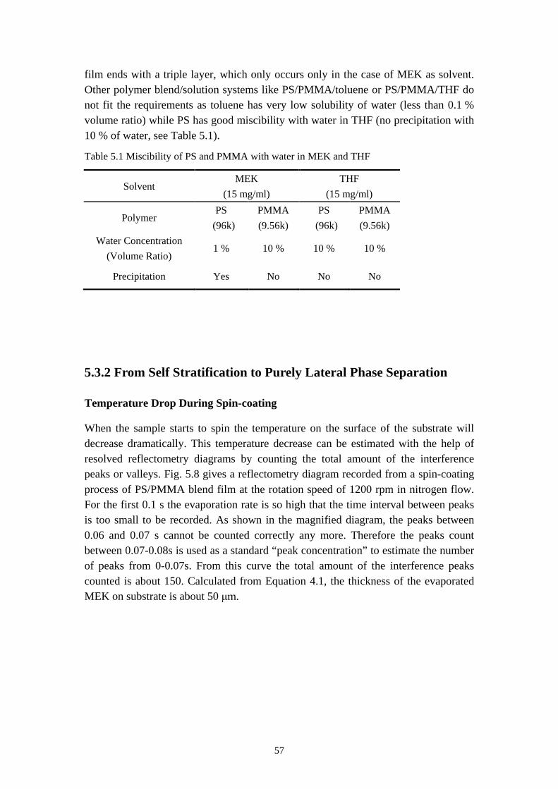
57
film ends with a triple layer, which only occurs only in the case of MEK as solvent. Other polymer blend/solution systems like PS/PMMA/toluene or PS/PMMA/THF do not fit the requirements as toluene has very low solubility of water (less than 0.1 % volume ratio) while PS has good miscibility with water in THF (no precipitation with 10 % of water, see Table 5.1).
Table 5.1 Miscibility of PS and PMMA with water in MEK and THF
Solvent MEK
(15 mg/ml) THF
(15 mg/ml)
Polymer PS
(96k) PMMA (9.56k)
PS (96k)
PMMA (9.56k)
Water Concentration (Volume Ratio)
1 % 10 % 10 % 10 %
Precipitation Yes No No No
5.3.2 From Self Stratification to Purely Lateral Phase Separation
Temperature Drop During Spin-coating
When the sample starts to spin the temperature on the surface of the substrate will decrease dramatically. This temperature decrease can be estimated with the help of resolved reflectometry diagrams by counting the total amount of the interference peaks or valleys. Fig. 5.8 gives a reflectometry diagram recorded from a spin-coating process of PS/PMMA blend film at the rotation speed of 1200 rpm in nitrogen flow. For the first 0.1 s the evaporation rate is so high that the time interval between peaks is too small to be recorded. As shown in the magnified diagram, the peaks between 0.06 and 0.07 s cannot be counted correctly any more. Therefore the peaks count between 0.07-0.08s is used as a standard “peak concentration” to estimate the number of peaks from 0-0.07s. From this curve the total amount of the interference peaks counted is about 150. Calculated from Equation 4.1, the thickness of the evaporated MEK on substrate is about 50 μm.
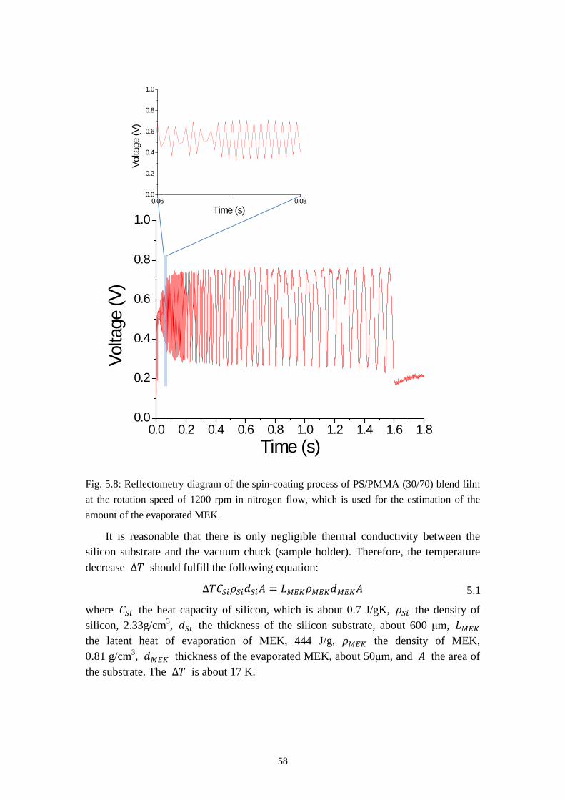
58
Fig. 5.8: Reflectometry diagram of the spin-coating process of PS/PMMA (30/70) blend film at the rotation speed of 1200 rpm in nitrogen flow, which is used for the estimation of the amount of the evaporated MEK.
It is reasonable that there is only negligible thermal conductivity between the silicon substrate and the vacuum chuck (sample holder). Therefore, the temperature decrease ∆𝑇 should fulfill the following equation:
∆𝑇𝐶𝑆𝑖𝜌𝑆𝑖𝑑𝑆𝑖𝐴 = 𝐿𝑀𝐸𝐾𝜌𝑀𝐸𝐾𝑑𝑀𝐸𝐾𝐴
where 𝐶𝑆𝑖 the heat capacity of silicon, which is about 0.7 J/gK, 𝜌𝑆𝑖 the density of silicon, 2.33g/cm3, 𝑑𝑆𝑖 the thickness of the silicon substrate, about 600 μm, 𝐿𝑀𝐸𝐾 the latent heat of evaporation of MEK, 444 J/g, 𝜌𝑀𝐸𝐾 the density of MEK, 0.81 g/cm3
, 𝑑𝑀𝐸𝐾 thickness of the evaporated MEK, about 50μm, and 𝐴 the area of the substrate. The ∆𝑇 is about 17 K.
0.0 0.2 0.4 0.6 0.8 1.0 1.2 1.4 1.6 1.80.0
0.2
0.4
0.6
0.8
1.0
Volta
ge (V
)
Time (s)
0.06 0.080.0
0.2
0.4
0.6
0.8
1.0
Volta
ge (V
)
Time (s)
5.1
59
The dew point can be calculated using the following equation [125]:
𝑡𝑑 = 𝑡 −100 − 𝑅𝐻
5
where 𝑡𝑑 is the dew point in centigrade, 𝑡 the room temperature in centigrade and 𝑅𝐻 the relative humidity. Since room temperature in the lab is about 22 ˚C, with a decrease of 17 ˚C the water condensation will start if the relative humidity is higher than 20 %.
Model of Purely Lateral Phase Separation
The model of the development of the film spun-cast at humid environment is described in Fig. 5.9. When the sample starts to spin, the water condensation begins at the humidity over 20 % (see Fig. 5.9b). If the humidity is over about 35 %, a 3-dimensional phase separation occurs between PS/MEK and PMMA/MEK/water phases. The PS molecules start the precipitation before they reach the middle of the solvent (see Fig. 5.9c). These PS/MEK phases agglomerate sometimes into larger ones (see Fig. 5.9d). With the further evaporation of MEK, the PS/MEK and PMMA/MEK/water phases reach the same height before when the PS/MEK can still keep the spherical shape (see Fig. 5.9e). Finally a Swiss Cheese Structure is formed after the complete solidification of the polymers while the PS islands end with an ellipsoidal shape (see Fig. 5.9f).
The spin casting humidity plays the most important role in the determination of the lateral structure in the PS/PMMA film as it affects the amount of the condensed water. With the help of this model, it can be easily drawn an explanation of the morphology development of PS/PMMA found and described in Fig. 5.5.2a. When the humidity reaches 60 %, the Swiss Cheese Structure is formed together with the breath figure (see Fig. 5.3.2e). The network structure formed at the humidity of 30 % (see Fig. 5.5.1g), however can be simply explained by the model shown in Fig. 5.6: the increased amount of water will expand the PMMA tunnels in PS layer and thus change the perforated film into a network. Since the water-rich layer forms in both of the models (see Fig. 5.6, 5.8) and the PS always tend to move to the middle, the only difference in the self-stratification and the 3-dimensional models is the time t0 when the PS starts to precipitate. Therefore a critical time t0c is defined by us where the structure formation mechanism follows the self-stratification model if t0 < t0c and the 3-dimensional phase separation model if t0 > tc0
.
5.2
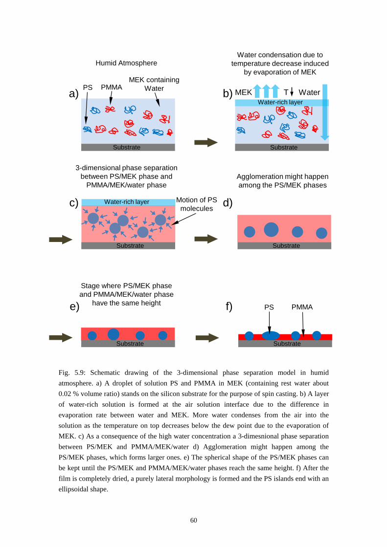
60
Fig. 5.9: Schematic drawing of the 3-dimensional phase separation model in humid atmosphere. a) A droplet of solution PS and PMMA in MEK (containing rest water about 0.02 % volume ratio) stands on the silicon substrate for the purpose of spin casting. b) A layer of water-rich solution is formed at the air solution interface due to the difference in evaporation rate between water and MEK. More water condenses from the air into the solution as the temperature on top decreases below the dew point due to the evaporation of MEK. c) As a consequence of the high water concentration a 3-dimesnional phase separation between PS/MEK and PMMA/MEK/water d) Agglomeration might happen among the PS/MEK phases, which forms larger ones. e) The spherical shape of the PS/MEK phases can be kept until the PS/MEK and PMMA/MEK/water phases reach the same height. f) After the film is completely dried, a purely lateral morphology is formed and the PS islands end with an ellipsoidal shape.
Substrate
PS PMMAMEK containing
Water
Substrate
MEK WaterTa) b)
c) d)
Water condensation due to temperature decrease induced
by evaporation of MEK
e) f)
Substrate
Water-rich layer
Substrate
Substrate Substrate
3-dimensional phase separation between PS/MEK phase and
PMMA/MEK/water phaseAgglomeration might happen among the PS/MEK phases
Stage where PS/MEK phase and PMMA/MEK/water phase
have the same height PS PMMA
Motion of PS molecules
Water-rich layer
Humid Atmosphere
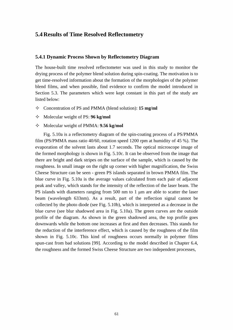
61
5.4 Results of Time Resolved Reflectometry
5.4.1 Dynamic Process Shown by Reflectometry Diagram
The house-built time resolved reflectometer was used in this study to monitor the drying process of the polymer blend solution during spin-coating. The motivation is to get time-resolved information about the formation of the morphologies of the polymer blend films, and when possible, find evidence to confirm the model introduced in Section 5.3. The parameters which were kept constant in this part of the study are listed below:
Concentration of PS and PMMA (blend solution): 15 mg/ml
Molecular weight of PS: 96 kg/mol
Molecular weight of PMMA: 9.56 kg/mol
Fig. 5.10a is a reflectometry diagram of the spin-coating process of a PS/PMMA film (PS/PMMA mass ratio 40/60, rotation speed 1200 rpm at humidity of 45 %). The evaporation of the solvent lasts about 1.7 seconds. The optical microscope image of the formed morphology is shown in Fig. 5.10c. It can be observed from the image that there are bright and dark stripes on the surface of the sample, which is caused by the roughness. In small image on the right up corner with higher magnification, the Swiss Cheese Structure can be seen - green PS islands separated in brown PMMA film. The blue curve in Fig. 5.10a is the average values calculated from each pair of adjacent peak and valley, which stands for the intensity of the reflection of the laser beam. The PS islands with diameters ranging from 500 nm to 1 μm are able to scatter the laser beam (wavelength 633nm). As a result, part of the reflection signal cannot be collected by the photo diode (see Fig. 5.10b), which is interpreted as a decrease in the blue curve (see blur shadowed area in Fig. 5.10a). The green curves are the outside profile of the diagram. As shown in the green shadowed area, the top profile goes downwards while the bottom one increases at first and then decreases. This stands for the reduction of the interference effect, which is caused by the roughness of the film shown in Fig. 5.10c. This kind of roughness occurs normally in polymer films spun-cast from bad solutions [99]. According to the model described in Chapter 6.4, the roughness and the formed Swiss Cheese Structure are two independent processes,
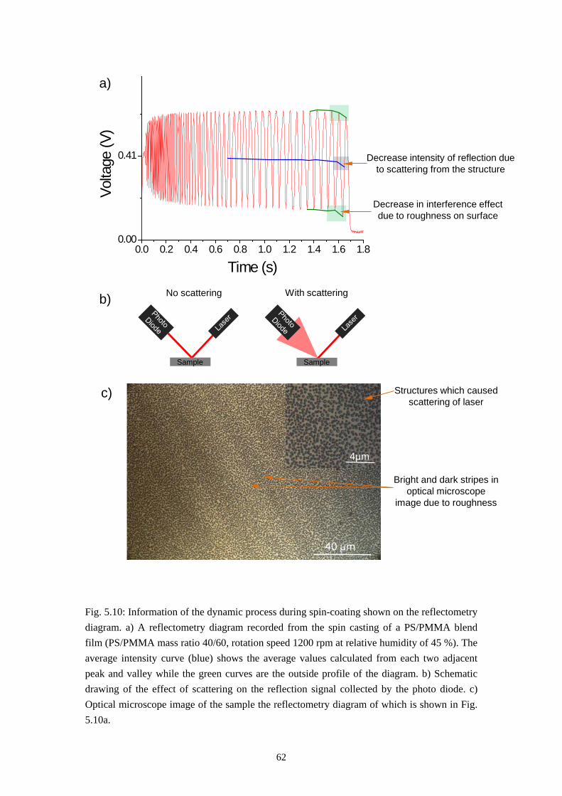
62
Fig. 5.10: Information of the dynamic process during spin-coating shown on the reflectometry diagram. a) A reflectometry diagram recorded from the spin casting of a PS/PMMA blend film (PS/PMMA mass ratio 40/60, rotation speed 1200 rpm at relative humidity of 45 %). The average intensity curve (blue) shows the average values calculated from each two adjacent peak and valley while the green curves are the outside profile of the diagram. b) Schematic drawing of the effect of scattering on the reflection signal collected by the photo diode. c) Optical microscope image of the sample the reflectometry diagram of which is shown in Fig. 5.10a.
0.0 0.2 0.4 0.6 0.8 1.0 1.2 1.4 1.6 1.80.00
0.41
Volta
ge (V
)
Time (s)
a)
Decrease in interference effect due to roughness on surface
Decrease intensity of reflection due to scattering from the structure
Sample Sample
b) No scattering With scattering
4μm
c) Structures which caused scattering of laser
Bright and dark stripes in optical microscope
image due to roughness
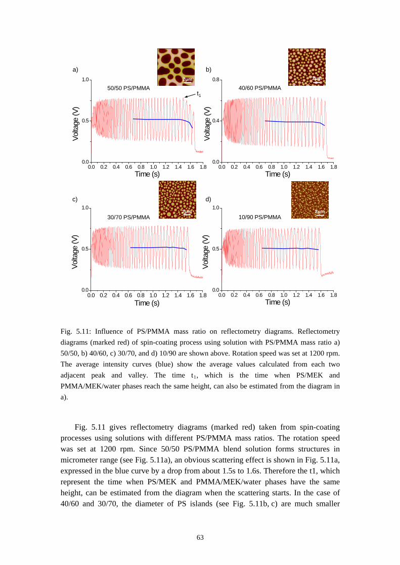
63
Fig. 5.11: Influence of PS/PMMA mass ratio on reflectometry diagrams. Reflectometry diagrams (marked red) of spin-coating process using solution with PS/PMMA mass ratio a) 50/50, b) 40/60, c) 30/70, and d) 10/90 are shown above. Rotation speed was set at 1200 rpm. The average intensity curves (blue) show the average values calculated from each two adjacent peak and valley. The time t1
, which is the time when PS/MEK and PMMA/MEK/water phases reach the same height, can also be estimated from the diagram in a).
Fig. 5.11 gives reflectometry diagrams (marked red) taken from spin-coating processes using solutions with different PS/PMMA mass ratios. The rotation speed was set at 1200 rpm. Since 50/50 PS/PMMA blend solution forms structures in micrometer range (see Fig. 5.11a), an obvious scattering effect is shown in Fig. 5.11a, expressed in the blue curve by a drop from about 1.5s to 1.6s. Therefore the t1, which represent the time when PS/MEK and PMMA/MEK/water phases have the same height, can be estimated from the diagram when the scattering starts. In the case of 40/60 and 30/70, the diameter of PS islands (see Fig. 5.11b, c) are much smaller
0.0 0.2 0.4 0.6 0.8 1.0 1.2 1.4 1.6 1.80.0
0.5
1.0Vo
ltage
(V)
Time (s)0.0 0.2 0.4 0.6 0.8 1.0 1.2 1.4 1.6 1.8
0.0
0.5
1.0
Volta
ge (V
)
Time (s)
0.0 0.2 0.4 0.6 0.8 1.0 1.2 1.4 1.6 1.80.0
0.4
0.8
Volta
ge (V
)
Time (s)0.0 0.2 0.4 0.6 0.8 1.0 1.2 1.4 1.6 1.8
0.0
0.5
1.0Vo
ltage
(V)
Time (s)
a) b)
c) d)
50/50 PS/PMMA 40/60 PS/PMMA
30/70 PS/PMMA 10/90 PS/PMMA2μm2μm
2μm2μm
t1
64
comparing with the structure of Fig. 5.11a and therefore less scattering effect at the end of the evaporation can be detected by the time-resolved reflectometer. For even smaller structures fabricated from PS/PMMA 10/90 solution, the blue line remains constant, meaning no observable scattering at all.
The reflectometry diagram of spin-coating process of PS/PMMA at humidity of 65 % is shown in Fig. 5.12. Some of PS islands agglomerate into bigger ones and thus leads to a strong decrease in reflection intensity (see area shadowed in dark blue in Fig. 5.12). In the light blue shadowed area, an increase in the reflection intensity occurs when the film is almost completely solidified. This is due to the evaporation of water, which is very slow at the humidity of 65 %.
Fig. 5.12 Reflectometry diagram of spin-coating process at relative humidity of 65 %. The PS/PMMA mass ratio was 40/60 and the rotation speed 1500 rpm. The average intensity curves (blue) show the average values calculated from each two adjacent peak and valley.
0.0 0.5 1.0 1.5 2.00.0
0.5
1.0
Volta
ge (V
)
Time (s)
Decrease intensity of reflection due to scattering
from the structure
Evaporation of water
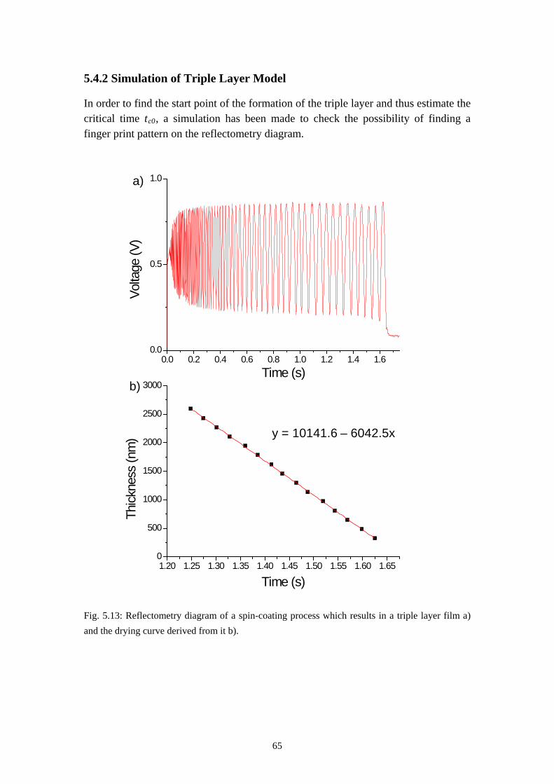
65
5.4.2 Simulation of Triple Layer Model
In order to find the start point of the formation of the triple layer and thus estimate the critical time tc0
, a simulation has been made to check the possibility of finding a finger print pattern on the reflectometry diagram.
Fig. 5.13: Reflectometry diagram of a spin-coating process which results in a triple layer film a) and the drying curve derived from it b).
0.0 0.2 0.4 0.6 0.8 1.0 1.2 1.4 1.60.0
0.5
1.0
Volta
ge (V
)
Time (s)
1.20 1.25 1.30 1.35 1.40 1.45 1.50 1.55 1.60 1.650
500
1000
1500
2000
2500
3000
Thick
ness
(nm
)
Time (s)
y = 10141.6 – 6042.5x
a)
b)
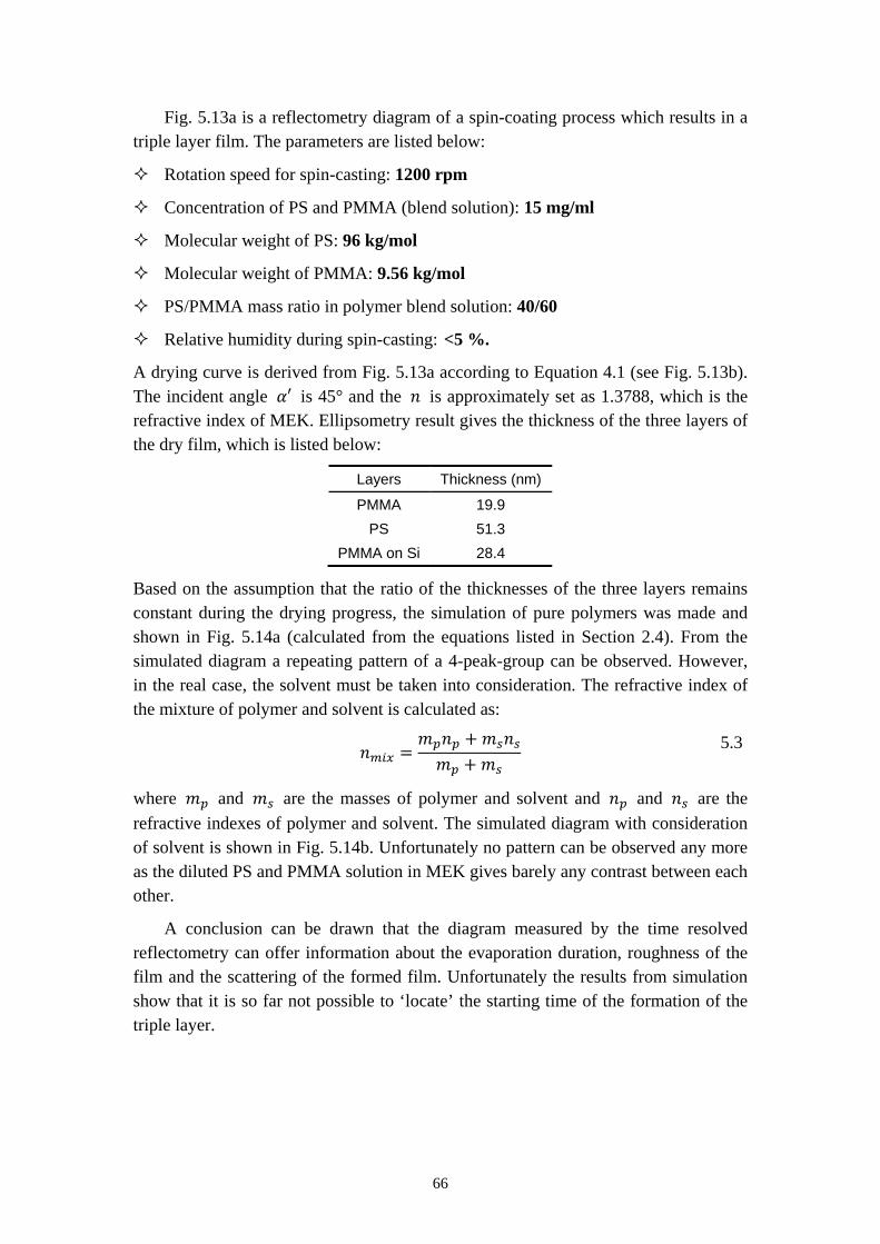
66
Fig. 5.13a is a reflectometry diagram of a spin-coating process which results in a triple layer film. The parameters are listed below:
Rotation speed for spin-casting: 1200 rpm
Concentration of PS and PMMA (blend solution): 15 mg/ml
Molecular weight of PS: 96 kg/mol
Molecular weight of PMMA: 9.56 kg/mol
PS/PMMA mass ratio in polymer blend solution: 40/60
Relative humidity during spin-casting: <5 %.
A drying curve is derived from Fig. 5.13a according to Equation 4.1 (see Fig. 5.13b). The incident angle 𝛼′ is 45° and the 𝑛 is approximately set as 1.3788, which is the refractive index of MEK. Ellipsometry result gives the thickness of the three layers of the dry film, which is listed below:
Layers Thickness (nm)
PMMA 19.9 PS 51.3
PMMA on Si 28.4
Based on the assumption that the ratio of the thicknesses of the three layers remains constant during the drying progress, the simulation of pure polymers was made and shown in Fig. 5.14a (calculated from the equations listed in Section 2.4). From the simulated diagram a repeating pattern of a 4-peak-group can be observed. However, in the real case, the solvent must be taken into consideration. The refractive index of the mixture of polymer and solvent is calculated as:
𝑛𝑚𝑖𝑥 =𝑚𝑝𝑛𝑝 + 𝑚𝑠𝑛𝑠𝑚𝑝 + 𝑚𝑠
where 𝑚𝑝 and 𝑚𝑠 are the masses of polymer and solvent and 𝑛𝑝 and 𝑛𝑠 are the refractive indexes of polymer and solvent. The simulated diagram with consideration of solvent is shown in Fig. 5.14b. Unfortunately no pattern can be observed any more as the diluted PS and PMMA solution in MEK gives barely any contrast between each other.
A conclusion can be drawn that the diagram measured by the time resolved reflectometry can offer information about the evaporation duration, roughness of the film and the scattering of the formed film. Unfortunately the results from simulation show that it is so far not possible to ‘locate’ the starting time of the formation of the triple layer.
5.3
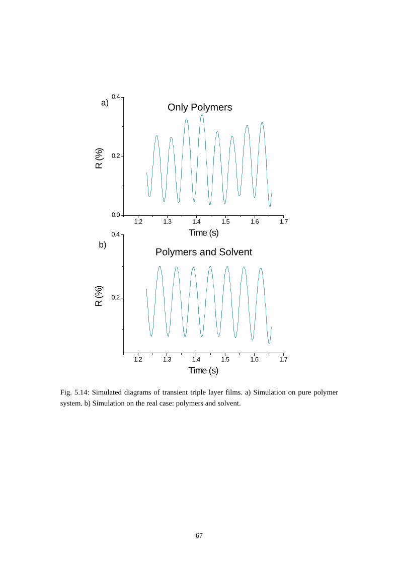
67
Fig. 5.14: Simulated diagrams of transient triple layer films. a) Simulation on pure polymer system. b) Simulation on the real case: polymers and solvent.
1.2 1.3 1.4 1.5 1.6 1.70.0
0.2
0.4R
(%)
Time (s)
1.2 1.3 1.4 1.5 1.6 1.7
0.2
0.4
R (%
)
Time (s)
a)
b)
Only Polymers
Polymers and Solvent

68
69
5.5 Reproduction of the Purely Lateral Phase Separation on
PS/PVP/MEK System
As the Swiss Cheese Structure is a unique case of a purely lateral phase separation, it will be very interesting to test if it is possible to obtain the same structure with other polymer blend systems. In order to test how general the 3-dimensional phase separation model is, we used again a polar and a less polar polymer which are soluble in MEK and fabricated the polymer film with spin-coating. PVP was selected to replace PMMA due to its high polarity (higher than PMMA). The parameters of the PS/PVP solution in MEK and the spin-casting are listed below:
Rotation speed for spin-casting: 1500 rpm
Concentration of PS and PVP (blend solution): 15 mg/ml
Molecular weight of PS: 96 kg/mol
Molecular weight of PVP: 11.1 kg/mol
PS/PVP mass ratio in polymer blend solution: 30/70
Relative humidity during spin-casting: 35 %.
Fig. 5.15 shows the result of the spin-casting. The Swiss Cheese Structure was successfully reproduced on PS/PVP system (see Fig. 5.15a). Cyclohexane and ethanol were used as the selective solvent for PS and PVP. After rinsing with a selective solvent, either a PVP film with holes or a PS islands array is left on the silicon substrate (see Fig. 5.15c, d). The only difference between the Swiss Cheese Structures of PS/PMMA and the PS/PVP systems is the shape of PS islands (see Fig. 5.16). Since the miscibility between PS and PVP is even lower than PS and PMMA, the precipitation of the PS starts earlier and therefore the islands can keep the spherical shape until the PVP film is nearly completely dried. This leads to a high topographical contrast between PS and PVP compared to PS in the PMMA matrix.
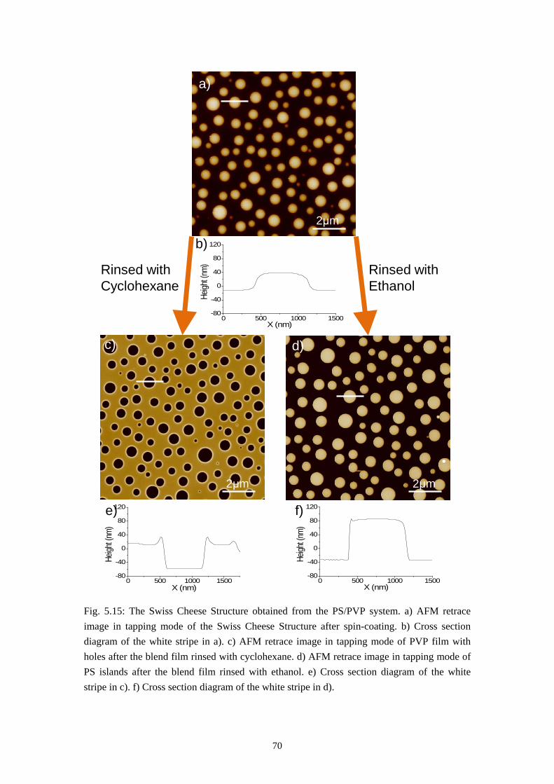
70
Fig. 5.15: The Swiss Cheese Structure obtained from the PS/PVP system. a) AFM retrace image in tapping mode of the Swiss Cheese Structure after spin-coating. b) Cross section diagram of the white stripe in a). c) AFM retrace image in tapping mode of PVP film with holes after the blend film rinsed with cyclohexane. d) AFM retrace image in tapping mode of PS islands after the blend film rinsed with ethanol. e) Cross section diagram of the white stripe in c). f) Cross section diagram of the white stripe in d).
2μm
2μm 2μm
0 500 1000 1500-80
-40
0
40
80
120
Heigh
t (nm)
X (nm)
0 500 1000 1500-80
-40
0
40
80
120
Heigh
t (nm)
X (nm)
0 500 1000 1500-80
-40
0
40
80
120
Heigh
t (nm)
X (nm)
Rinsed with Ethanol
Rinsed with Cyclohexane
a)
c) d)
b)
e) f)
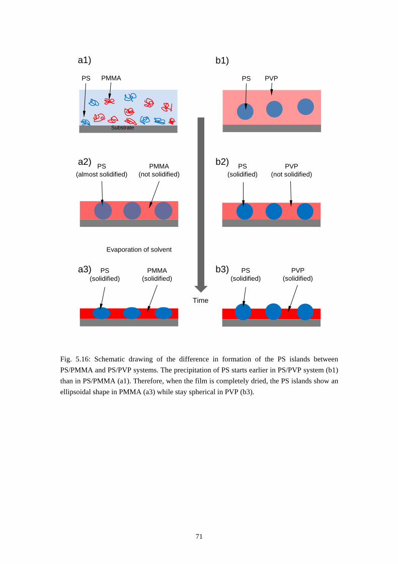
71
Fig. 5.16: Schematic drawing of the difference in formation of the PS islands between PS/PMMA and PS/PVP systems. The precipitation of PS starts earlier in PS/PVP system (b1) than in PS/PMMA (a1). Therefore, when the film is completely dried, the PS islands show an ellipsoidal shape in PMMA (a3) while stay spherical in PVP (b3).
PMMA (not solidified)
PS (almost solidified)
PS (solidified)
PVP(not solidified)
PS (solidified)
PMMA (solidified)
PS (solidified)
PVP (solidified)
Evaporation of solvent
a1) b1)
b2)a2)
Substrate
PS PMMA PS PVP
b3)a3)
Time

72
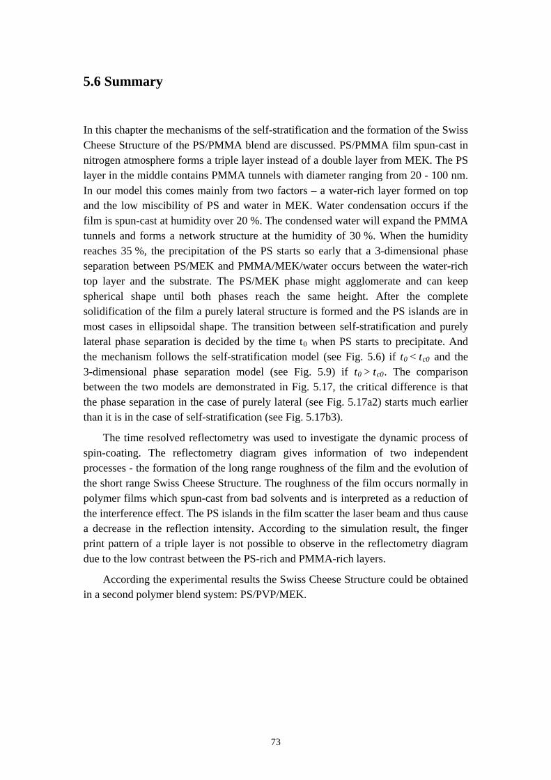
73
5.6 Summary
In this chapter the mechanisms of the self-stratification and the formation of the Swiss Cheese Structure of the PS/PMMA blend are discussed. PS/PMMA film spun-cast in nitrogen atmosphere forms a triple layer instead of a double layer from MEK. The PS layer in the middle contains PMMA tunnels with diameter ranging from 20 - 100 nm. In our model this comes mainly from two factors – a water-rich layer formed on top and the low miscibility of PS and water in MEK. Water condensation occurs if the film is spun-cast at humidity over 20 %. The condensed water will expand the PMMA tunnels and forms a network structure at the humidity of 30 %. When the humidity reaches 35 %, the precipitation of the PS starts so early that a 3-dimensional phase separation between PS/MEK and PMMA/MEK/water occurs between the water-rich top layer and the substrate. The PS/MEK phase might agglomerate and can keep spherical shape until both phases reach the same height. After the complete solidification of the film a purely lateral structure is formed and the PS islands are in most cases in ellipsoidal shape. The transition between self-stratification and purely lateral phase separation is decided by the time t0 when PS starts to precipitate. And the mechanism follows the self-stratification model (see Fig. 5.6) if t0 < tc0 and the 3-dimensional phase separation model (see Fig. 5.9) if t0 > tc0
The time resolved reflectometry was used to investigate the dynamic process of spin-coating. The reflectometry diagram gives information of two independent processes - the formation of the long range roughness of the film and the evolution of the short range Swiss Cheese Structure. The roughness of the film occurs normally in polymer films which spun-cast from bad solvents and is interpreted as a reduction of the interference effect. The PS islands in the film scatter the laser beam and thus cause a decrease in the reflection intensity. According to the simulation result, the finger print pattern of a triple layer is not possible to observe in the reflectometry diagram due to the low contrast between the PS-rich and PMMA-rich layers.
. The comparison between the two models are demonstrated in Fig. 5.17, the critical difference is that the phase separation in the case of purely lateral (see Fig. 5.17a2) starts much earlier than it is in the case of self-stratification (see Fig. 5.17b3).
According the experimental results the Swiss Cheese Structure could be obtained in a second polymer blend system: PS/PVP/MEK.
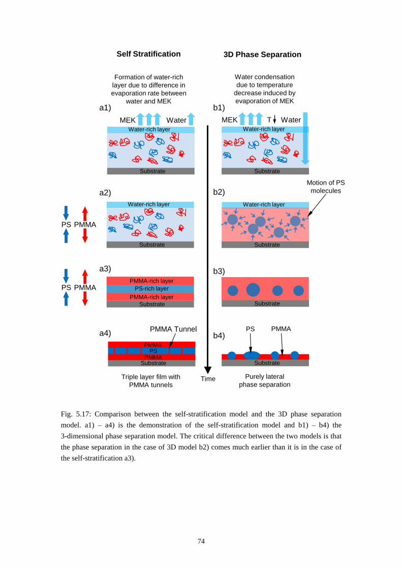
74
Fig. 5.17: Comparison between the self-stratification model and the 3D phase separation model. a1) – a4) is the demonstration of the self-stratification model and b1) – b4) the 3-dimensional phase separation model. The critical difference between the two models is that the phase separation in the case of 3D model b2) comes much earlier than it is in the case of the self-stratification a3).
Substrate
MEK WaterT
Water condensation due to temperature
decrease induced by evaporation of MEK
Water-rich layer
Motion of PS molecules
Substrate
Substrate
PS PMMA
Purely lateral phase separation
Substrate
MEK WaterWater-rich layer
Formation of water-rich layer due to difference in evaporation rate between
water and MEK
Substrate
Water-rich layer
PS PMMA
SubstratePMMA-rich layer
PMMA-rich layerPS-rich layerPS PMMA
SubstratePMMA
PMMAPS
PMMA Tunnel
Triple layer film with PMMA tunnels
Self Stratification 3D Phase Separation
Time
a1) b1)
a2)
a3)
a4)
b2)
b3)
b4)
Substrate
Water-rich layer
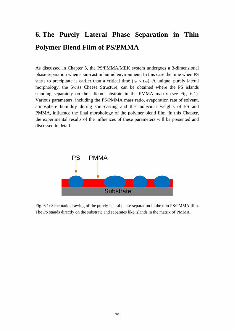
75
6. The Purely Lateral Phase Separation in Thin
Polymer Blend Film of PS/PMMA
As discussed in Chapter 5, the PS/PMMA/MEK system undergoes a 3-dimensional phase separation when spun-cast in humid environment. In this case the time when PS starts to precipitate is earlier than a critical time (t0 < tc0
). A unique, purely lateral morphology, the Swiss Cheese Structure, can be obtained where the PS islands standing separately on the silicon substrate in the PMMA matrix (see Fig. 6.1). Various parameters, including the PS/PMMA mass ratio, evaporation rate of solvent, atmosphere humidity during spin-casting and the molecular weights of PS and PMMA, influence the final morphology of the polymer blend film. In this Chapter, the experimental results of the influences of these parameters will be presented and discussed in detail.
Fig. 6.1: Schematic drawing of the purely lateral phase separation in the thin PS/PMMA film. The PS stands directly on the substrate and separates like islands in the matrix of PMMA.
PS PMMA
Substrate
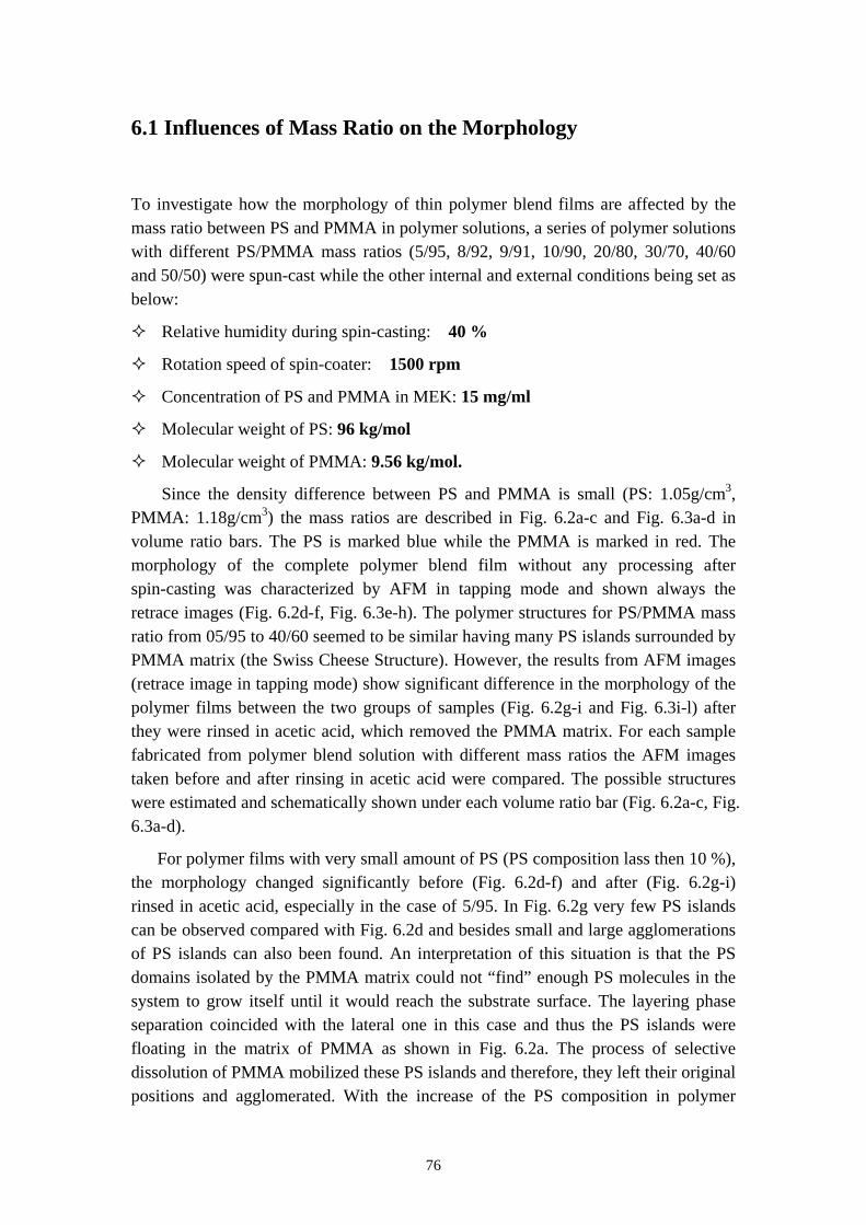
76
6.1 Influences of Mass Ratio on the Morphology
To investigate how the morphology of thin polymer blend films are affected by the mass ratio between PS and PMMA in polymer solutions, a series of polymer solutions with different PS/PMMA mass ratios (5/95, 8/92, 9/91, 10/90, 20/80, 30/70, 40/60 and 50/50) were spun-cast while the other internal and external conditions being set as below:
Relative humidity during spin-casting: 40 %
Rotation speed of spin-coater: 1500 rpm
Concentration of PS and PMMA in MEK: 15 mg/ml
Molecular weight of PS: 96 kg/mol
Molecular weight of PMMA: 9.56 kg/mol.
Since the density difference between PS and PMMA is small (PS: 1.05g/cm3, PMMA: 1.18g/cm3
For polymer films with very small amount of PS (PS composition lass then 10 %), the morphology changed significantly before (Fig. 6.2d-f) and after (Fig. 6.2g-i) rinsed in acetic acid, especially in the case of 5/95. In Fig. 6.2g very few PS islands can be observed compared with Fig. 6.2d and besides small and large agglomerations of PS islands can also been found. An interpretation of this situation is that the PS domains isolated by the PMMA matrix could not “find” enough PS molecules in the system to grow itself until it would reach the substrate surface. The layering phase separation coincided with the lateral one in this case and thus the PS islands were floating in the matrix of PMMA as shown in Fig. 6.2a. The process of selective dissolution of PMMA mobilized these PS islands and therefore, they left their original positions and agglomerated. With the increase of the PS composition in polymer
) the mass ratios are described in Fig. 6.2a-c and Fig. 6.3a-d in volume ratio bars. The PS is marked blue while the PMMA is marked in red. The morphology of the complete polymer blend film without any processing after spin-casting was characterized by AFM in tapping mode and shown always the retrace images (Fig. 6.2d-f, Fig. 6.3e-h). The polymer structures for PS/PMMA mass ratio from 05/95 to 40/60 seemed to be similar having many PS islands surrounded by PMMA matrix (the Swiss Cheese Structure). However, the results from AFM images (retrace image in tapping mode) show significant difference in the morphology of the polymer films between the two groups of samples (Fig. 6.2g-i and Fig. 6.3i-l) after they were rinsed in acetic acid, which removed the PMMA matrix. For each sample fabricated from polymer blend solution with different mass ratios the AFM images taken before and after rinsing in acetic acid were compared. The possible structures were estimated and schematically shown under each volume ratio bar (Fig. 6.2a-c, Fig. 6.3a-d).
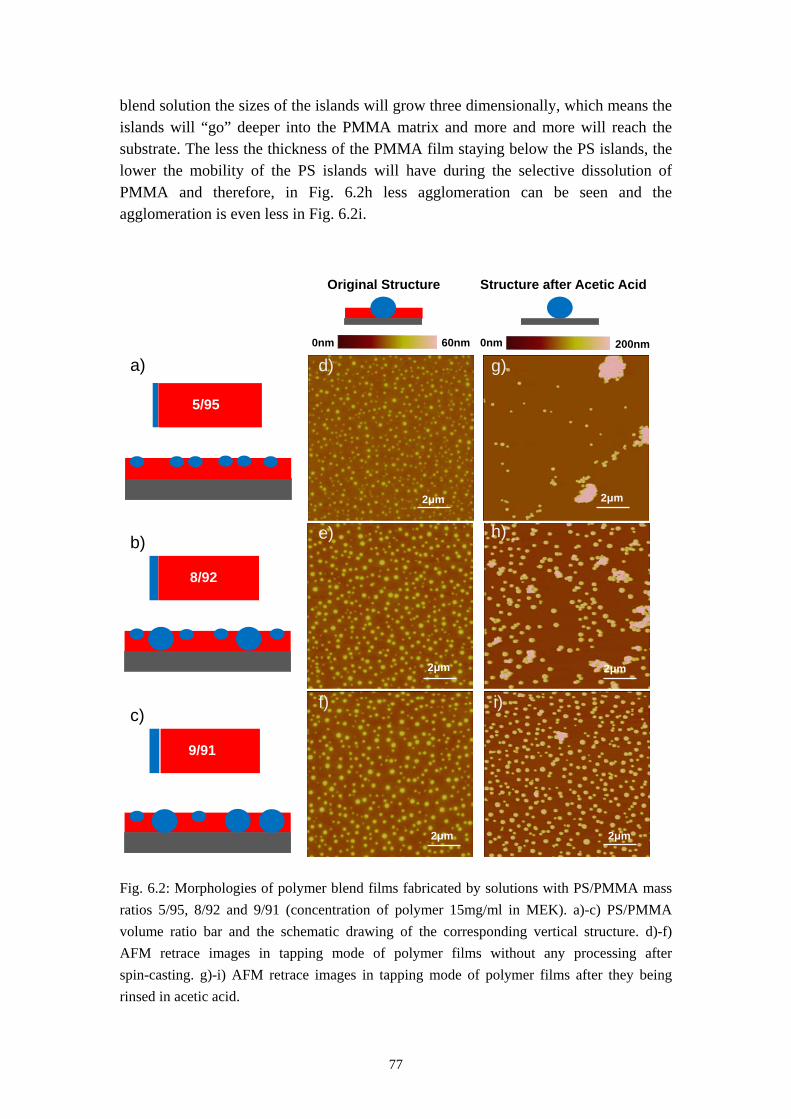
77
blend solution the sizes of the islands will grow three dimensionally, which means the islands will “go” deeper into the PMMA matrix and more and more will reach the substrate. The less the thickness of the PMMA film staying below the PS islands, the lower the mobility of the PS islands will have during the selective dissolution of PMMA and therefore, in Fig. 6.2h less agglomeration can be seen and the agglomeration is even less in Fig. 6.2i.
Fig. 6.2: Morphologies of polymer blend films fabricated by solutions with PS/PMMA mass ratios 5/95, 8/92 and 9/91 (concentration of polymer 15mg/ml in MEK). a)-c) PS/PMMA volume ratio bar and the schematic drawing of the corresponding vertical structure. d)-f) AFM retrace images in tapping mode of polymer films without any processing after spin-casting. g)-i) AFM retrace images in tapping mode of polymer films after they being rinsed in acetic acid.
5/95
2μm
0nm 60nm
2μm
0nm 200nm
8/92
2μm 2μm
9/91
2μm2μm
Original Structure Structure after Acetic Acid
a)
b)
c)
d)
e)
f)
g)
h)
i)
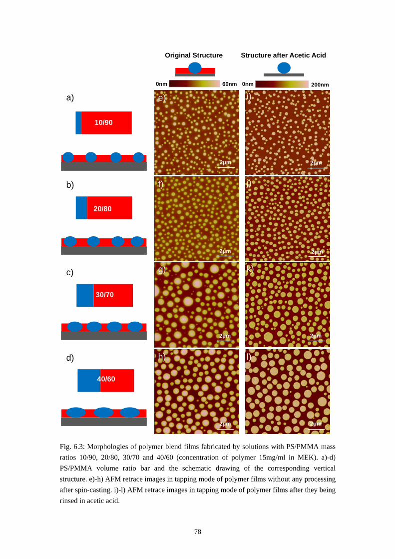
78
Fig. 6.3: Morphologies of polymer blend films fabricated by solutions with PS/PMMA mass ratios 10/90, 20/80, 30/70 and 40/60 (concentration of polymer 15mg/ml in MEK). a)-d) PS/PMMA volume ratio bar and the schematic drawing of the corresponding vertical structure. e)-h) AFM retrace images in tapping mode of polymer films without any processing after spin-casting. i)-l) AFM retrace images in tapping mode of polymer films after they being rinsed in acetic acid.
10/90
2μm 2μm
20/80
2μm2μm
30/70
2μm2μm
40/60
2μm 2μm
0nm 60nm 0nm 200nm
Original Structure Structure after Acetic Acid
a)
b)
c)
d)
e)
f)
g)
h) l)
k)
j)
i)
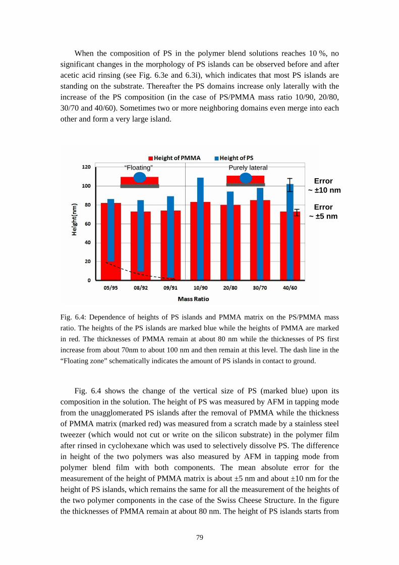
79
When the composition of PS in the polymer blend solutions reaches 10 %, no significant changes in the morphology of PS islands can be observed before and after acetic acid rinsing (see Fig. 6.3e and 6.3i), which indicates that most PS islands are standing on the substrate. Thereafter the PS domains increase only laterally with the increase of the PS composition (in the case of PS/PMMA mass ratio 10/90, 20/80, 30/70 and 40/60). Sometimes two or more neighboring domains even merge into each other and form a very large island.
Fig. 6.4: Dependence of heights of PS islands and PMMA matrix on the PS/PMMA mass ratio. The heights of the PS islands are marked blue while the heights of PMMA are marked in red. The thicknesses of PMMA remain at about 80 nm while the thicknesses of PS first increase from about 70nm to about 100 nm and then remain at this level. The dash line in the “Floating zone” schematically indicates the amount of PS islands in contact to ground.
Fig. 6.4 shows the change of the vertical size of PS (marked blue) upon its composition in the solution. The height of PS was measured by AFM in tapping mode from the unagglomerated PS islands after the removal of PMMA while the thickness of PMMA matrix (marked red) was measured from a scratch made by a stainless steel tweezer (which would not cut or write on the silicon substrate) in the polymer film after rinsed in cyclohexane which was used to selectively dissolve PS. The difference in height of the two polymers was also measured by AFM in tapping mode from polymer blend film with both components. The mean absolute error for the measurement of the height of PMMA matrix is about ±5 nm and about ±10 nm for the height of PS islands, which remains the same for all the measurement of the heights of the two polymer components in the case of the Swiss Cheese Structure. In the figure the thicknesses of PMMA remain at about 80 nm. The height of PS islands starts from
“Floating” Purely lateral
Error ~ ±10 nm
Error ~ ±5 nm
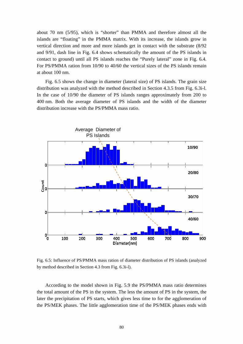
80
about 70 nm (5/95), which is “shorter” than PMMA and therefore almost all the islands are “floating” in the PMMA matrix. With its increase, the islands grow in vertical direction and more and more islands get in contact with the substrate (8/92 and 9/91, dash line in Fig. 6.4 shows schematically the amount of the PS islands in contact to ground) until all PS islands reaches the “Purely lateral” zone in Fig. 6.4. For PS/PMMA ration from 10/90 to 40/60 the vertical sizes of the PS islands remain at about 100 nm.
Fig. 6.5 shows the change in diameter (lateral size) of PS islands. The grain size distribution was analyzed with the method described in Section 4.3.5 from Fig. 6.3i-l. In the case of 10/90 the diameter of PS islands ranges approximately from 200 to 400 nm. Both the average diameter of PS islands and the width of the diameter distribution increase with the PS/PMMA mass ratio.
Fig. 6.5: Influence of PS/PMMA mass ration of diameter distribution of PS islands (analyzed by method described in Section 4.3 from Fig. 6.3i-l).
According to the model shown in Fig. 5.9 the PS/PMMA mass ratio determines the total amount of the PS in the system. The less the amount of PS in the system, the later the precipitation of PS starts, which gives less time to for the agglomeration of the PS/MEK phases. The little agglomeration time of the PS/MEK phases ends with
10/90
20/80
30/70
40/60
Average Diameter of PS Islands
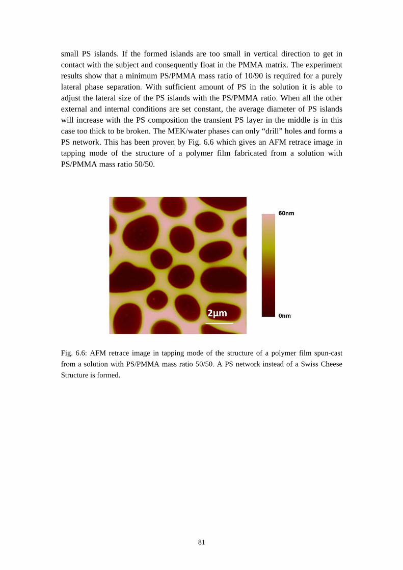
81
small PS islands. If the formed islands are too small in vertical direction to get in contact with the subject and consequently float in the PMMA matrix. The experiment results show that a minimum PS/PMMA mass ratio of 10/90 is required for a purely lateral phase separation. With sufficient amount of PS in the solution it is able to adjust the lateral size of the PS islands with the PS/PMMA ratio. When all the other external and internal conditions are set constant, the average diameter of PS islands will increase with the PS composition the transient PS layer in the middle is in this case too thick to be broken. The MEK/water phases can only “drill” holes and forms a PS network. This has been proven by Fig. 6.6 which gives an AFM retrace image in tapping mode of the structure of a polymer film fabricated from a solution with PS/PMMA mass ratio 50/50.
Fig. 6.6: AFM retrace image in tapping mode of the structure of a polymer film spun-cast from a solution with PS/PMMA mass ratio 50/50. A PS network instead of a Swiss Cheese Structure is formed.

82
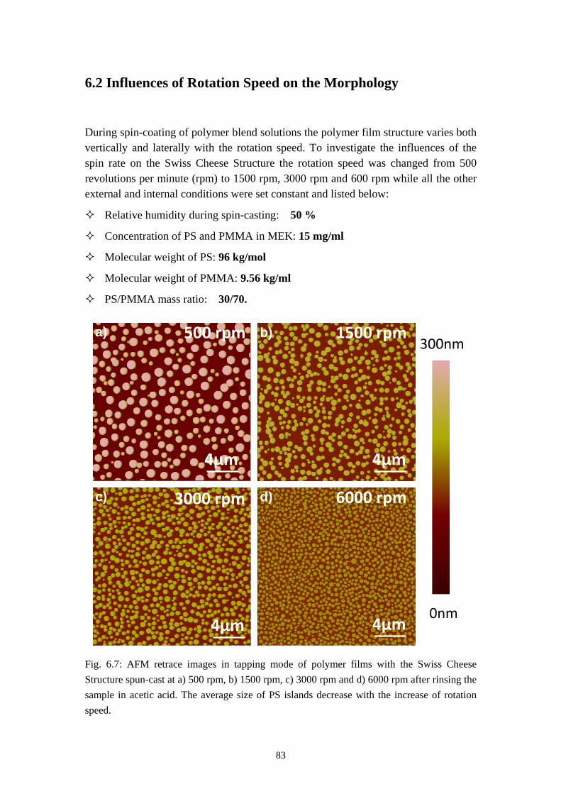
83
6.2 Influences of Rotation Speed on the Morphology
During spin-coating of polymer blend solutions the polymer film structure varies both vertically and laterally with the rotation speed. To investigate the influences of the spin rate on the Swiss Cheese Structure the rotation speed was changed from 500 revolutions per minute (rpm) to 1500 rpm, 3000 rpm and 600 rpm while all the other external and internal conditions were set constant and listed below:
Relative humidity during spin-casting: 50 %
Concentration of PS and PMMA in MEK: 15 mg/ml
Molecular weight of PS: 96 kg/mol
Molecular weight of PMMA: 9.56 kg/ml
PS/PMMA mass ratio: 30/70.
Fig. 6.7: AFM retrace images in tapping mode of polymer films with the Swiss Cheese Structure spun-cast at a) 500 rpm, b) 1500 rpm, c) 3000 rpm and d) 6000 rpm after rinsing the sample in acetic acid. The average size of PS islands decrease with the increase of rotation speed.
3000 rpm
4μm 4μm
6000 rpm
500 rpm
4μm
1500 rpm
4μm
0nm
300nma)
c)
b)
d)
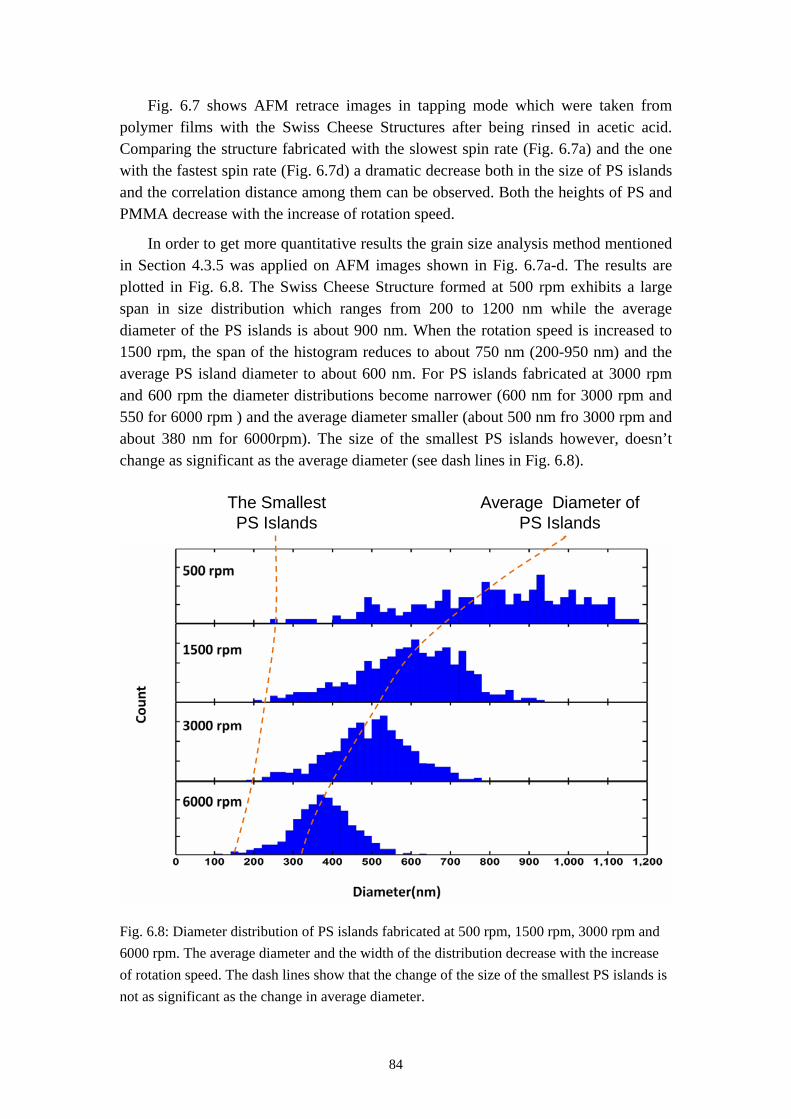
84
Fig. 6.7 shows AFM retrace images in tapping mode which were taken from polymer films with the Swiss Cheese Structures after being rinsed in acetic acid. Comparing the structure fabricated with the slowest spin rate (Fig. 6.7a) and the one with the fastest spin rate (Fig. 6.7d) a dramatic decrease both in the size of PS islands and the correlation distance among them can be observed. Both the heights of PS and PMMA decrease with the increase of rotation speed.
In order to get more quantitative results the grain size analysis method mentioned in Section 4.3.5 was applied on AFM images shown in Fig. 6.7a-d. The results are plotted in Fig. 6.8. The Swiss Cheese Structure formed at 500 rpm exhibits a large span in size distribution which ranges from 200 to 1200 nm while the average diameter of the PS islands is about 900 nm. When the rotation speed is increased to 1500 rpm, the span of the histogram reduces to about 750 nm (200-950 nm) and the average PS island diameter to about 600 nm. For PS islands fabricated at 3000 rpm and 600 rpm the diameter distributions become narrower (600 nm for 3000 rpm and 550 for 6000 rpm ) and the average diameter smaller (about 500 nm fro 3000 rpm and about 380 nm for 6000rpm). The size of the smallest PS islands however, doesn’t change as significant as the average diameter (see dash lines in Fig. 6.8).
Fig. 6.8: Diameter distribution of PS islands fabricated at 500 rpm, 1500 rpm, 3000 rpm and 6000 rpm. The average diameter and the width of the distribution decrease with the increase of rotation speed. The dash lines show that the change of the size of the smallest PS islands is not as significant as the change in average diameter.
Average Diameter of PS Islands
The Smallest PS Islands
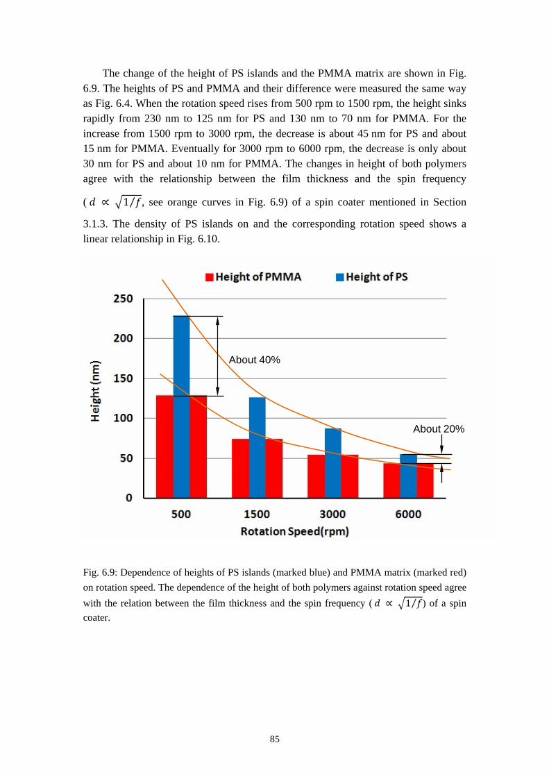
85
The change of the height of PS islands and the PMMA matrix are shown in Fig. 6.9. The heights of PS and PMMA and their difference were measured the same way as Fig. 6.4. When the rotation speed rises from 500 rpm to 1500 rpm, the height sinks rapidly from 230 nm to 125 nm for PS and 130 nm to 70 nm for PMMA. For the increase from 1500 rpm to 3000 rpm, the decrease is about 45 nm for PS and about 15 nm for PMMA. Eventually for 3000 rpm to 6000 rpm, the decrease is only about 30 nm for PS and about 10 nm for PMMA. The changes in height of both polymers agree with the relationship between the film thickness and the spin frequency
( 𝑑 ∝ �1 𝑓⁄ , see orange curves in Fig. 6.9) of a spin coater mentioned in Section
3.1.3. The density of PS islands on and the corresponding rotation speed shows a linear relationship in Fig. 6.10.
Fig. 6.9: Dependence of heights of PS islands (marked blue) and PMMA matrix (marked red) on rotation speed. The dependence of the height of both polymers against rotation speed agree with the relation between the film thickness and the spin frequency ( 𝑑 ∝ �1 𝑓⁄ ) of a spin coater.
About 40%
About 20%
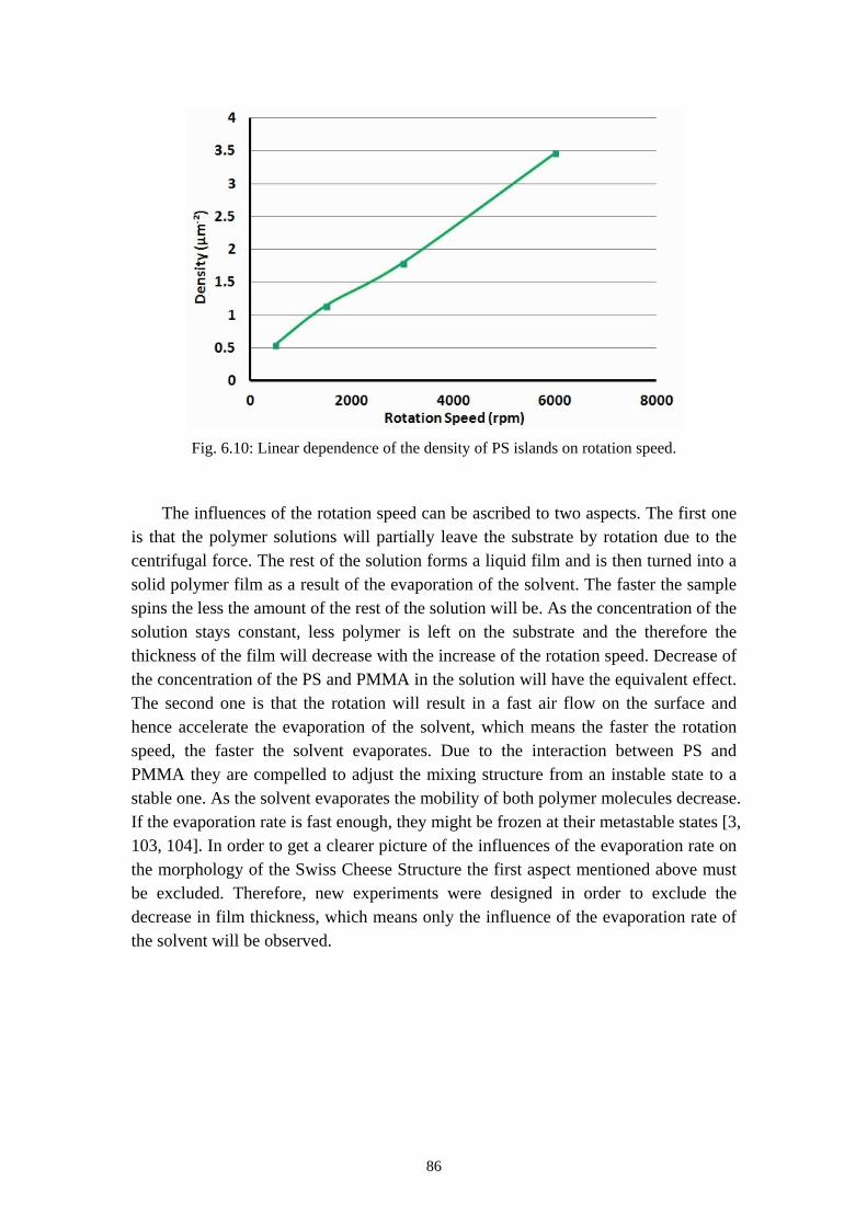
86
Fig. 6.10: Linear dependence of the density of PS islands on rotation speed.
The influences of the rotation speed can be ascribed to two aspects. The first one is that the polymer solutions will partially leave the substrate by rotation due to the centrifugal force. The rest of the solution forms a liquid film and is then turned into a solid polymer film as a result of the evaporation of the solvent. The faster the sample spins the less the amount of the rest of the solution will be. As the concentration of the solution stays constant, less polymer is left on the substrate and the therefore the thickness of the film will decrease with the increase of the rotation speed. Decrease of the concentration of the PS and PMMA in the solution will have the equivalent effect. The second one is that the rotation will result in a fast air flow on the surface and hence accelerate the evaporation of the solvent, which means the faster the rotation speed, the faster the solvent evaporates. Due to the interaction between PS and PMMA they are compelled to adjust the mixing structure from an instable state to a stable one. As the solvent evaporates the mobility of both polymer molecules decrease. If the evaporation rate is fast enough, they might be frozen at their metastable states [3, 103, 104]. In order to get a clearer picture of the influences of the evaporation rate on the morphology of the Swiss Cheese Structure the first aspect mentioned above must be excluded. Therefore, new experiments were designed in order to exclude the decrease in film thickness, which means only the influence of the evaporation rate of the solvent will be observed.
87
6.3 Influences of Evaporation Rate on the Morphology
As discussed in Section 5.2, the rotation speed of the spin coater affects the morphology of the polymer film in two aspects, the film thickness and the evaporation rate. In order to investigate the influences of the evaporation rate exclusively a new experiment was designed. Since the effect of reduction in film thickness can be compromised by changing the concentration of PS and PMMA in the polymer blend solution a series of concentrations were set and the rotation speed of the spin coater were changed correspondingly in order to have a series of films with approximately the same thickness. Due to the limit of the solubility of polymer and the fact that lateral structures cannot be formed when the concentration of the solution is too low [105, 106], the series of concentrations were chosen as 10 mg/ml, 15 mg/ml, 20 mg/ml and 25 mg/ml. The other internal and external conditions were set constant and listed below:
Relative humidity during spin-casting: 50 %
Solvent of the polymer blend solution: MEK
Molecular weight of PS: 35.7 kg/mol
Molecular weight of PMMA: 9.56 kg/mol
PS/PMMA mass ratio: 30/70.
The polystyrene with relatively low molecular weight was selected in the experiment. A film with the Swiss Cheese Structure was first spun-cast from solution with concentration of 10 mg/ml at rotation speed of 900 rpm. The thickness of PS and PMMA was measured by AFM in tapping mode from the films which were treated with selective dissolution process (acetic acid to dissolve PMMA and cyclohexane to PS). The average film thickness of PS and PMMA was about 75 nm. Then a higher rotation speed was applied for solution with concentration of 15 mg/ml in order to have a polymer blend film with the same average thickness of PS and PMMA. Proven by the results of AFM measurement the film spun-cast from solution with concentration of 15 mg/ml at rotation speed of 2000 rpm, from 20 mg/ml solution at 3400 rpm and from 25 mg/ml solution at 6800 rpm fulfilled this requirement. The evaporation time needed until the film becomes solid was measured with the time resolved reflectometer which records the evolution of the film thickness during the spin-casting process (mentioned in Section 4.4). The evaporation time needed is 1.92 s at rotation speed of 900 rpm, 0.89 s at 2000 rpm, 0.52 s at 3400 rpm and 0.31 s at 6800 rpm (plotted in Fig. 6.11e).
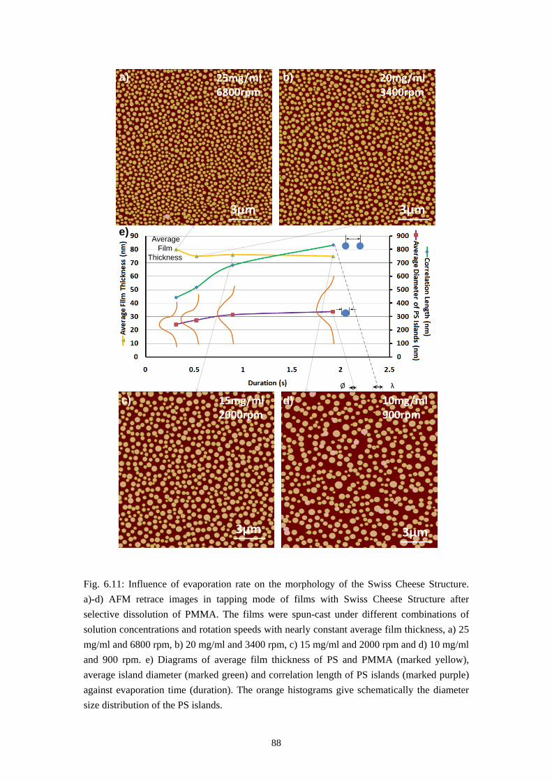
88
Fig. 6.11: Influence of evaporation rate on the morphology of the Swiss Cheese Structure. a)-d) AFM retrace images in tapping mode of films with Swiss Cheese Structure after selective dissolution of PMMA. The films were spun-cast under different combinations of solution concentrations and rotation speeds with nearly constant average film thickness, a) 25 mg/ml and 6800 rpm, b) 20 mg/ml and 3400 rpm, c) 15 mg/ml and 2000 rpm and d) 10 mg/ml and 900 rpm. e) Diagrams of average film thickness of PS and PMMA (marked yellow), average island diameter (marked green) and correlation length of PS islands (marked purple) against evaporation time (duration). The orange histograms give schematically the diameter size distribution of the PS islands.
15mg/ml 2000rpm
3μm
20mg/ml 3400rpm
3μm
25mg/ml 6800rpm
3μm
10mg/ml 900rpm
3μm
Ø λ
a) b)
d)c)
e)Average
Film Thickness
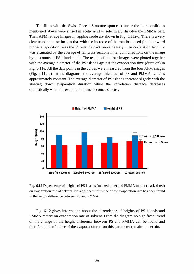
89
The films with the Swiss Cheese Structure spun-cast under the four conditions mentioned above were rinsed in acetic acid to selectively dissolve the PMMA part. Their AFM retrace images in tapping mode are shown in Fig. 6.11a-d. There is a very clear trend in these images that with the increase of the rotation speed (in other word higher evaporation rate) the PS islands pack more densely. The correlation length λ was estimated by the average of ten cross sections in random directions on the image by the counts of PS islands on it. The results of the four images were plotted together with the average diameter of the PS islands against the evaporation time (duration) in Fig. 6.11e. All the data points in the curves were measured from the four AFM images (Fig. 6.11a-d). In the diagrams, the average thickness of PS and PMMA remains approximately constant. The average diameter of PS islands increase slightly with the slowing down evaporation duration while the correlation distance decreases dramatically when the evaporation time becomes shorter.
Fig. 6.12 Dependence of heights of PS islands (marked blue) and PMMA matrix (marked red) on evaporation rate of solvent. No significant influence of the evaporation rate has been found in the height difference between PS and PMMA.
Fig. 6.12 gives information about the dependence of heights of PS islands and PMMA matrix on evaporation rate of solvent. From the diagram no significant trend of the change of the height difference between PS and PMMA can be found and therefore, the influence of the evaporation rate on this parameter remains uncertain.
Error ~ ±10 nm
Error ~ ±5 nm
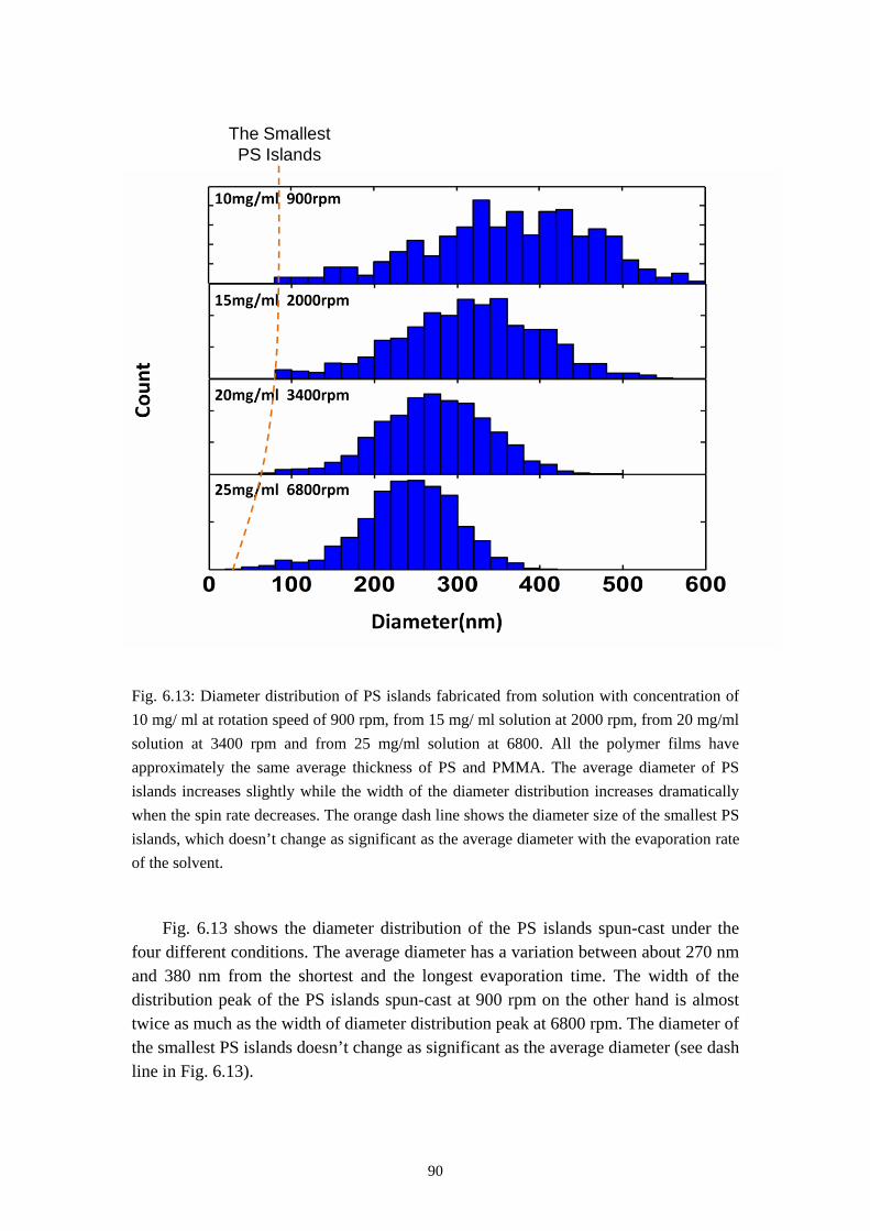
90
Fig. 6.13: Diameter distribution of PS islands fabricated from solution with concentration of 10 mg/ ml at rotation speed of 900 rpm, from 15 mg/ ml solution at 2000 rpm, from 20 mg/ml solution at 3400 rpm and from 25 mg/ml solution at 6800. All the polymer films have approximately the same average thickness of PS and PMMA. The average diameter of PS islands increases slightly while the width of the diameter distribution increases dramatically when the spin rate decreases. The orange dash line shows the diameter size of the smallest PS islands, which doesn’t change as significant as the average diameter with the evaporation rate of the solvent.
Fig. 6.13 shows the diameter distribution of the PS islands spun-cast under the four different conditions. The average diameter has a variation between about 270 nm and 380 nm from the shortest and the longest evaporation time. The width of the distribution peak of the PS islands spun-cast at 900 rpm on the other hand is almost twice as much as the width of diameter distribution peak at 6800 rpm. The diameter of the smallest PS islands doesn’t change as significant as the average diameter (see dash line in Fig. 6.13).
The Smallest PS Islands
91
According to the model (see Fig. 5.9) the PS/MEK phases might agglomerate into larger ones before they land onto the substrate and then form larger PS islands. The longer the time the PS/MEK phases have for the agglomeration, the higher the chance of the formation of larger PS islands. This agglomeration progress is however random and therefore in Fig. 6.13 PS islands with diameter of about 100 nm can always be found for all of the four conditions. At increasing of the evaporation rate, the whole drying process is shortened so the time which allows the PS/MEK phases to agglomerate becomes short. High evaporation rate means low degree of agglomeration of the PS/MEK phases, which results in small average diameter and narrower diameter size distribution of the islands and also small correlation distance between islands. Therefore, the evaporation rate is a very important parameter which helps to tune the diameter distribution of the PS islands in the Swiss Cheese Structure.

92
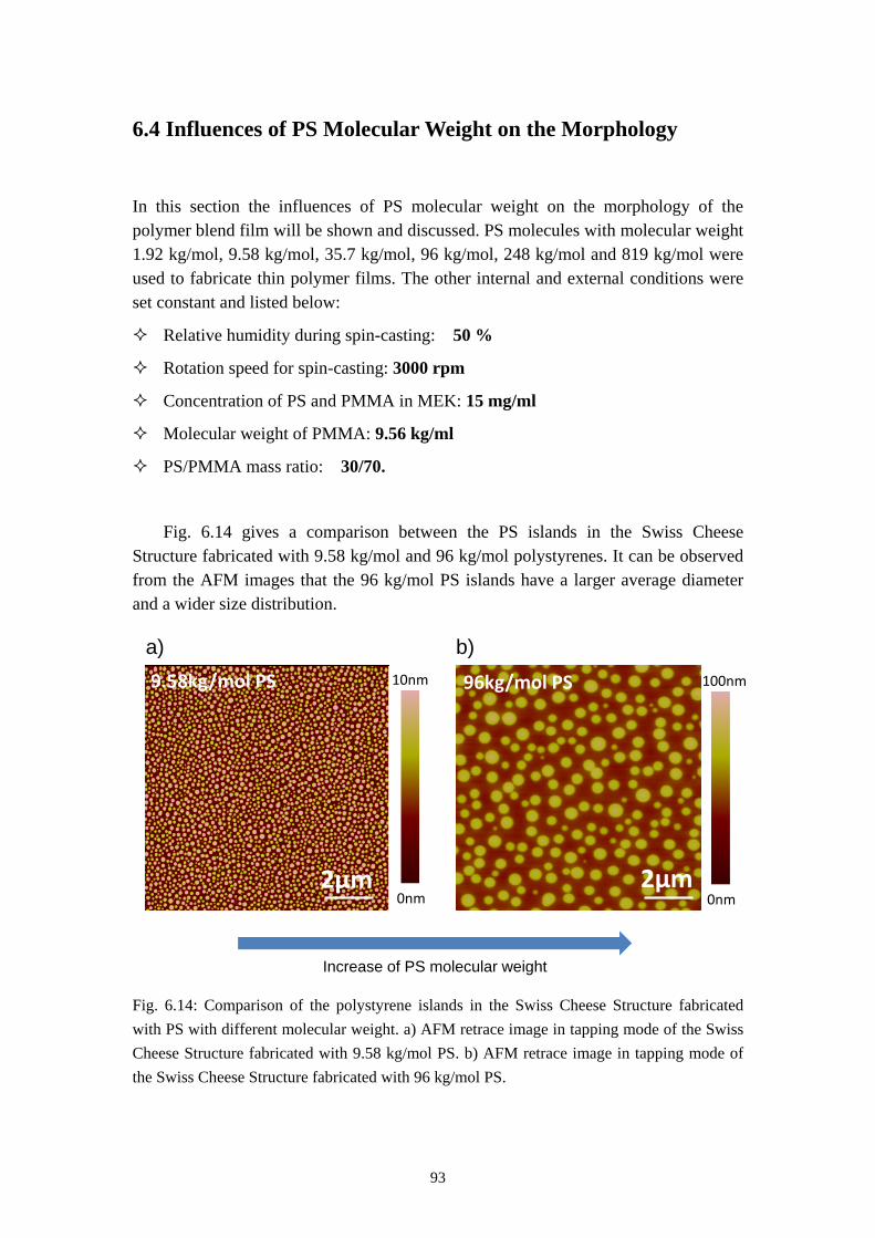
93
6.4 Influences of PS Molecular Weight on the Morphology
In this section the influences of PS molecular weight on the morphology of the polymer blend film will be shown and discussed. PS molecules with molecular weight 1.92 kg/mol, 9.58 kg/mol, 35.7 kg/mol, 96 kg/mol, 248 kg/mol and 819 kg/mol were used to fabricate thin polymer films. The other internal and external conditions were set constant and listed below:
Relative humidity during spin-casting: 50 %
Rotation speed for spin-casting: 3000 rpm
Concentration of PS and PMMA in MEK: 15 mg/ml
Molecular weight of PMMA: 9.56 kg/ml
PS/PMMA mass ratio: 30/70.
Fig. 6.14 gives a comparison between the PS islands in the Swiss Cheese Structure fabricated with 9.58 kg/mol and 96 kg/mol polystyrenes. It can be observed from the AFM images that the 96 kg/mol PS islands have a larger average diameter and a wider size distribution.
Fig. 6.14: Comparison of the polystyrene islands in the Swiss Cheese Structure fabricated with PS with different molecular weight. a) AFM retrace image in tapping mode of the Swiss Cheese Structure fabricated with 9.58 kg/mol PS. b) AFM retrace image in tapping mode of the Swiss Cheese Structure fabricated with 96 kg/mol PS.
2μm
10nm
0nm
9.58kg/mol PS
2μm
100nm
0nm
96kg/mol PS
a) b)
Increase of PS molecular weight
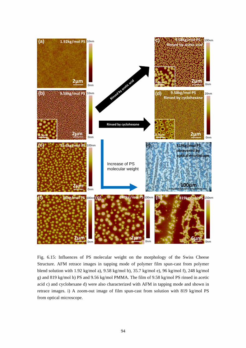
94
Fig. 6.15: Influences of PS molecular weight on the morphology of the Swiss Cheese Structure. AFM retrace images in tapping mode of polymer film spun-cast from polymer blend solution with 1.92 kg/mol a), 9.58 kg/mol b), 35.7 kg/mol e), 96 kg/mol f), 248 kg/mol g) and 819 kg/mol h) PS and 9.56 kg/mol PMMA. The film of 9.58 kg/mol PS rinsed in acetic acid c) and cyclohexane d) were also characterized with AFM in tapping mode and shown in retrace images. i) A zoom-out image of film spun-cast from solution with 819 kg/mol PS from optical microscope.
2μm
20nm
0nm
10nm
0nm
1.92kg/mol PS
2μm
2μm
100nm
0nm
35.6kg/mol PS
2μm
10nm
0nm
9.58kg/mol PS
0.5μm
2μm
100nm
0nm0.5μm
9.58kg/mol PSRinsed by cyclohexane
9.58kg/mol PSRinsed by acetic acid
Rinsed by cyclohexane
0.5μm
(a)
(b)
c)
(d)
2μm
100nm
0nm
248kg/mol PS (g)
2μm
100nm
0nm
96kg/mol PS (f)
(e)
6μm
150nm
0nm
819kg/mol PS (h)
819kg/mol PSobsevered by optical microscope
100μm
(i)
Increase of PS molecular weight
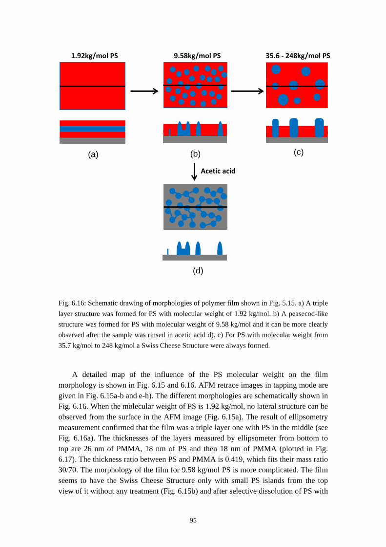
95
Fig. 6.16: Schematic drawing of morphologies of polymer film shown in Fig. 5.15. a) A triple layer structure was formed for PS with molecular weight of 1.92 kg/mol. b) A peasecod-like structure was formed for PS with molecular weight of 9.58 kg/mol and it can be more clearly observed after the sample was rinsed in acetic acid d). c) For PS with molecular weight from 35.7 kg/mol to 248 kg/mol a Swiss Cheese Structure were always formed.
A detailed map of the influence of the PS molecular weight on the film morphology is shown in Fig. 6.15 and 6.16. AFM retrace images in tapping mode are given in Fig. 6.15a-b and e-h). The different morphologies are schematically shown in Fig. 6.16. When the molecular weight of PS is 1.92 kg/mol, no lateral structure can be observed from the surface in the AFM image (Fig. 6.15a). The result of ellipsometry measurement confirmed that the film was a triple layer one with PS in the middle (see Fig. 6.16a). The thicknesses of the layers measured by ellipsometer from bottom to top are 26 nm of PMMA, 18 nm of PS and then 18 nm of PMMA (plotted in Fig. 6.17). The thickness ratio between PS and PMMA is 0.419, which fits their mass ratio 30/70. The morphology of the film for 9.58 kg/mol PS is more complicated. The film seems to have the Swiss Cheese Structure only with small PS islands from the top view of it without any treatment (Fig. 6.15b) and after selective dissolution of PS with
(a) (b) (c)
(d)
Acetic acid
1.92kg/mol PS 9.58kg/mol PS 35.6 - 248kg/mol PS
96
cyclohexane (Fig. 6.15d). In Fig. 6.15c however, the connections among neighboring PS islands hidden under the PMMA matrix are discovered after the sample was rinsed in acetic acid. These peasecod-like structures of PS islands were sketched both from top and in cross section in Fig. 6.16b and 6.14d. The reason of the formation of these bridges between PS islands remain uncertain, one possible reason is that it’s due to the fluctuation of the PS thin film. When the wavelength of the fluctuation is larger than the diameter of the islands, the interconnections between the islands remain in the solid film. In the case of PS with molecular weight 35.7 kg/ml, 96 kg/ml and 248 kg/ml the spun-cast films are always ended with the normal Swiss Cheese Structure (see in Fig. 6.15 e-g and sketched in 6.14c). The PS islands grow both laterally and vertically (see in Fig. 6.17) with the increase of PS molecular weight. No more connections among the neighboring islands were found. For the 819 kg/mol PS no more purely lateral phase was formed and the film shows a complicated dendrite-like structure which incorporates both vertical and lateral phase separations (see in Fig. 6.15h-i). Results from time resolved reflectometer show that the evaporation time of the solvent is about 0.8 s.
Fig. 6.17 gives information about the thicknesses of both polymers. The height difference of PS and PMMA changes significant from the 9.58 kg/mol to 35.6 kg/mol and 96 kg/mol. That is mainly due to the difference of the two polymers in the duration of solidification after the two phases reach the same height. The smaller the molecular weight, the higher the miscibility of the PS with PMMA/MEK/water phase. Therefore t0
becomes larger and the duration of solidification of PS takes is longer after the two phases reach the same height. Consequently the height difference between the two polymers becomes smaller. In the case of 248 kg/mol the height difference is even larger than the other ones, which is only because the growth of PS islands is in 3 dimensions.
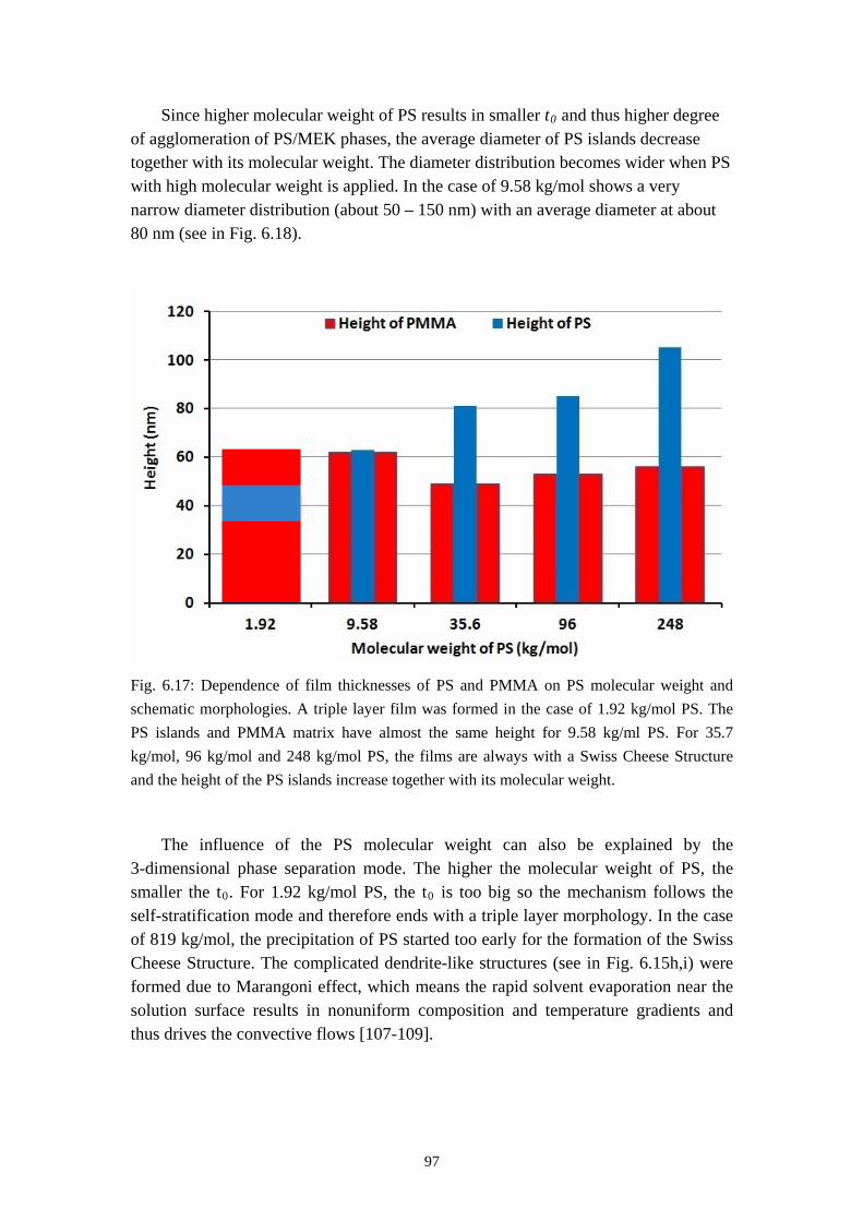
97
Since higher molecular weight of PS results in smaller t0
and thus higher degree of agglomeration of PS/MEK phases, the average diameter of PS islands decrease together with its molecular weight. The diameter distribution becomes wider when PS with high molecular weight is applied. In the case of 9.58 kg/mol shows a very narrow diameter distribution (about 50 – 150 nm) with an average diameter at about 80 nm (see in Fig. 6.18).
Fig. 6.17: Dependence of film thicknesses of PS and PMMA on PS molecular weight and schematic morphologies. A triple layer film was formed in the case of 1.92 kg/mol PS. The PS islands and PMMA matrix have almost the same height for 9.58 kg/ml PS. For 35.7 kg/mol, 96 kg/mol and 248 kg/mol PS, the films are always with a Swiss Cheese Structure and the height of the PS islands increase together with its molecular weight.
The influence of the PS molecular weight can also be explained by the 3-dimensional phase separation mode. The higher the molecular weight of PS, the smaller the t0. For 1.92 kg/mol PS, the t0 is too big so the mechanism follows the self-stratification mode and therefore ends with a triple layer morphology. In the case of 819 kg/mol, the precipitation of PS started too early for the formation of the Swiss Cheese Structure. The complicated dendrite-like structures (see in Fig. 6.15h,i) were formed due to Marangoni effect, which means the rapid solvent evaporation near the solution surface results in nonuniform composition and temperature gradients and thus drives the convective flows [107-109].
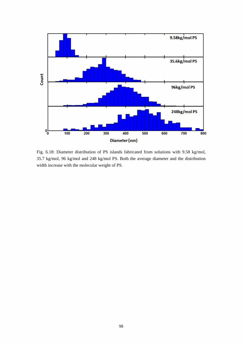
98
Fig. 6.18: Diameter distribution of PS islands fabricated from solutions with 9.58 kg/mol, 35.7 kg/mol, 96 kg/mol and 248 kg/mol PS. Both the average diameter and the distribution width increase with the molecular weight of PS.
99
6.5 The Dynamic Process of the Morphology Formation
As already shown in Chapter 5.2, the morphology of the polymer blend system depends strongly on the relative humidity during spin-casting. There is another parameter, the molecular weight of PMMA, which plays also an important role during the dynamic process of spin-coating. A series of experiments was designed and made under different combinations of these two parameters:
Rotation speed for spin-casting: 6800 rpm
Concentration of PS and PMMA (blend solution): 25 mg/ml
Molecular weight of PS: 96 kg/mol
Molecular weight of PMMA: 1.9 kg/mol, 9.56 kg/mol and 187 kg/mol
PS/PMMA mass ratio in polymer blend solution: 30/70
Relative humidity during spin-casting: 20 %, 30 %, 40 % and 50 %.
The samples were scanned by AFM in tapping mode and the retrace images are shown in Fig. 6.19. The molecular weight of PMMA increases along the horizontal direction while the relative humidity increases in vertical direction. The first column of AFM images (Fig. 6.19a1-a4) gives the results of samples spin-casted from PMMA with a molecular weight of 1.9 kg/mol. At the relative humidity of 10 % and 20 %, the polymer blend films show no lateral structure at all (see Fig. 6.19a1, a2). The samples were cut into two pieces and rinsed separately in acetic acid and cyclohexane. The cyclohexane didn’t affect the thickness of the film, which is similar to the results of film spun-cast in nitrogen flow (see Fig. 5.3.1a). However, the film was removed completely by acetic acid, which indicates that the PS didn’t form a layer spreading over the sample area but small structures floating in the PMMA matrix. At the humidity of 40 % the film surface becomes rough and is with very small holes (diameter below 50 nm) on it (see Fig. 6.20a3). Some of these holes became deeper after rinsed in cyclohexane, which is similar to the result shown in Fig. 6.21 for the case of PMMA with molecular weight of 187 kg/mol. When the humidity reaches 50 %, a network structure instead of the Swiss Cheese Structure is formed as shown in Fig. 6.3a4. The network was not destroyed by rinsing in acetic acid and therefore, the bones of the network is consisted of only PS. Results of the films fabricated from 1.9 kg/mol PMMA show that the Swiss Cheese Structure cannot be obtained at higher humidity.
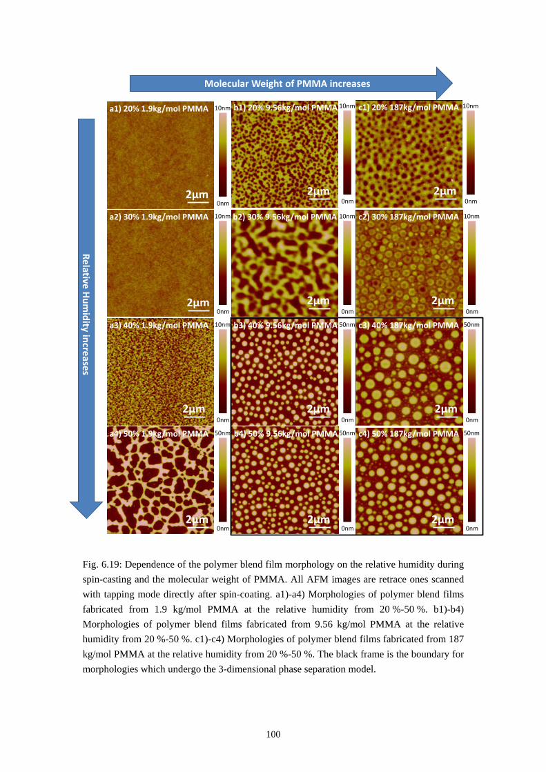
100
Fig. 6.19: Dependence of the polymer blend film morphology on the relative humidity during spin-casting and the molecular weight of PMMA. All AFM images are retrace ones scanned with tapping mode directly after spin-coating. a1)-a4) Morphologies of polymer blend films fabricated from 1.9 kg/mol PMMA at the relative humidity from 20 %-50 %. b1)-b4) Morphologies of polymer blend films fabricated from 9.56 kg/mol PMMA at the relative humidity from 20 %-50 %. c1)-c4) Morphologies of polymer blend films fabricated from 187 kg/mol PMMA at the relative humidity from 20 %-50 %. The black frame is the boundary for morphologies which undergo the 3-dimensional phase separation model.
a1) 20% 1.9kg/mol PMMA
2μm
10nm
0nm
a2) 30% 1.9kg/mol PMMA
2μm
10nm
0nm
2μm
a3) 40% 1.9kg/mol PMMA 10nm
0nm
2μm
a4) 50% 1.9kg/mol PMMA 50nm
0nm
2μm
b1) 20% 9.56kg/mol PMMA 10nm
0nm
2μm
b2) 30% 9.56kg/mol PMMA 10nm
0nm
2μm
b3) 40% 9.56kg/mol PMMA 50nm
0nm
2μm
b4) 50% 9.56kg/mol PMMA 50nm
0nm
2μm
c1) 20% 187kg/mol PMMA 10nm
0nm
2μm
c2) 30% 187kg/mol PMMA 10nm
0nm
2μm
c3) 40% 187kg/mol PMMA 50nm
0nm
2μm
c4) 50% 187kg/mol PMMA 50nm
0nm
Molecular Weight of PMMA increases
Relative Humidity increases
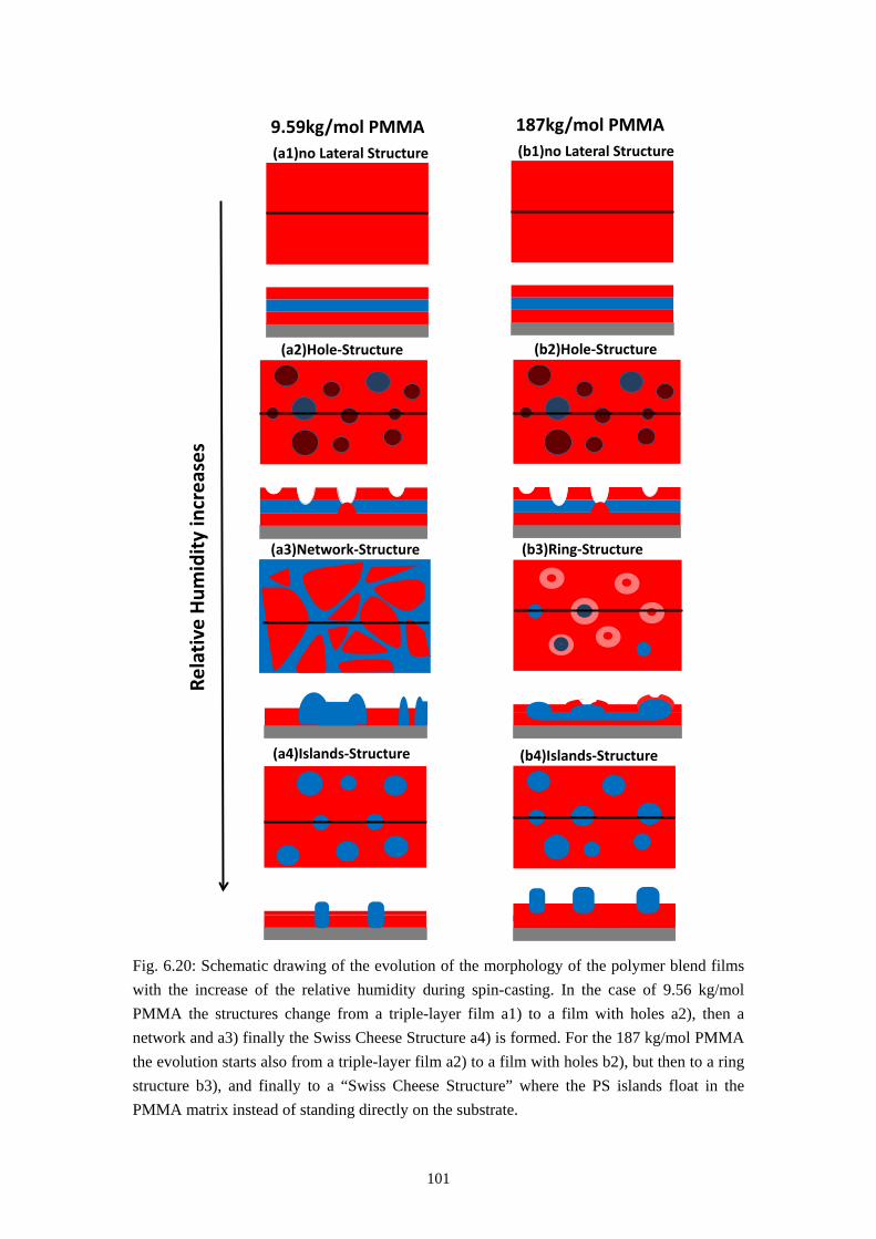
101
Fig. 6.20: Schematic drawing of the evolution of the morphology of the polymer blend films with the increase of the relative humidity during spin-casting. In the case of 9.56 kg/mol PMMA the structures change from a triple-layer film a1) to a film with holes a2), then a network and a3) finally the Swiss Cheese Structure a4) is formed. For the 187 kg/mol PMMA the evolution starts also from a triple-layer film a2) to a film with holes b2), but then to a ring structure b3), and finally to a “Swiss Cheese Structure” where the PS islands float in the PMMA matrix instead of standing directly on the substrate.
(a1)no Lateral Structure
(a3)Network-Structure
(a4)Islands-Structure
(a2)Hole-Structure
(b1)no Lateral Structure
(b2)Hole-Structure
(4)
(b4)Islands-Structure
Rela
tive
Hum
idity
incr
ease
s
9.59kg/mol PMMA 187kg/mol PMMA
(b3)Ring-Structure
102
For PMMA with molecular weight of 9.56 kg/mol, the evolution of the morphology starts from a triple layer film (as shown in Section 5.1) at the humidity of 20 % to a film with wholes (see Fig. 6.19b1), then to a network structure (see Fig. 6.19b2) and finally to the Swiss Cheese Structure at the relative humidity of 40 % (Fig. 6.19b3). The sample in Fig. 6.19b1 was rinsed in cyclohexane and the sample in Fig. 6.19b2 was rinsed in acetic acid. The results are very similar to the samples shown in Fig. 6.19a3 and 6.18a4, meaning the morphology revolutions of polymer blend film with the two PMMAs have these two common stages. The difference is that the two morphologies come at lower relative humidity in the case of 9.56 kg/mol PMMA. Therefore it is principally also possible to get the Swiss Cheese Structure by using 1.9 kg/mol PMMA at higher humidity (e.g. 60 %). However, the breath figures will then occur and the Swiss Cheese Structure is no longer “pure”.
In the case of PMMA with molecular weight of 187 kg/mol, a film with holes was formed at the relative humidity of 20 % (see Fig. 6.19c1). When the humidity was increased to 30 %, lots of ring like structures were found in the film (see Fig. 6.19c2). At the relative humidity of 40 % and 50 % the Swiss Cheese Structures were obtained. (Fig. 6.19c3,c4). However, the PS islands on the samples were washed away when rinsed in acetic acid, which means that there are PMMA layers underneath. The PS islands are floating in the PMMA matrix instead of standing directly on the substrate. Therefore the morphology cannot be regarded as a purely lateral phase separation.
A rinsing test in cyclohexane was made on a sample which has the similar structure as shown in Fig. 6.19c1. The result is given in Fig. 6.21. Fig. 6.21b shows the morphology of the sample after the rinsing test. Comparing to Fig. 6.5a, some of the holes became deeper, while the others remain the same. The film thickness stayed also still. The phenomenon can be explained schematically in Fig. 6.21c-f. There basically three kinds of holes in this kind of morphology:
1. The hole stays only in the top layer of PMMA.
2. The hole reaches the PS layer but not completely through it.
3. The hole reaches the bottom PMMA layer.
If the hole breaks through the PS layer, the PMMA in the bottom layer tends to reach the top layer through these holes. Therefore some of the holes are partially or completely filled with PMMA. Since the cyclohexane is a selective solvent for PS, the holes in the case of 1 and 3 mentioned above will not make any change. In the case of 2 the PS in the holes will be dissolved and subsequently the holes become deeper.
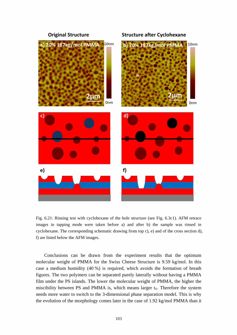
103
Fig. 6.21: Rinsing test with cyclohexane of the hole structure (see Fig. 6.3c1). AFM retrace images in tapping mode were taken before a) and after b) the sample was rinsed in cyclohexane. The corresponding schematic drawing from top c), e) and of the cross section d), f) are listed below the AFM images.
Conclusions can be drawn from the experiment results that the optimum molecular weight of PMMA for the Swiss Cheese Structure is 9.59 kg/mol. In this case a medium humidity (40 %) is required, which avoids the formation of breath figures. The two polymers can be separated purely laterally without having a PMMA film under the PS islands. The lower the molecular weight of PMMA, the higher the miscibility between PS and PMMA is, which means larger t0
2μm
a) 20% 187kg/mol PMMA 10nm
0nm2μm
b) 20% 187kg/mol PMMA 10nm
0nm
Structure after CyclohexaneOriginal Structure
c) d)
e) f)
. Therefore the system needs more water to switch to the 3-dimensional phase separation model. This is why the evolution of the morphology comes later in the case of 1.92 kg/mol PMMA than it
104
does in the other two. The hole-structure shown in Fig. 6.19b1 can be perfectly explained by the model shown in Fig. 5.6. At the humidity of 20 %, which is just over the threshold of the water condensation, the amount of the condensed water is too little to disturb the formation of the triple layer. The water in the bottom layer is “blocked” by the PS-rich layer in the middle. The evaporation of the water is thus retarded and leaves no relaxation time for the PMMA film. Consequently a film with breath figures is formed. At the humidity between of 30 %, 40 % and 50 % there is no longer retarding effect as the PS layer in the middle is broken by the MEK/water phases. Therefore, no breath figures can be found at the network-structure and the Swiss Cheese Structure. When the molecular weight of PMMA reaches 187 kg/mol however, the miscibility between PMMA and MEK decreases and hence the precipitation of PMMA starts earlier than the complete solidification of PS. Therefore a PMMA film can be found under the PS islands and the islands can only float in the Matrix.
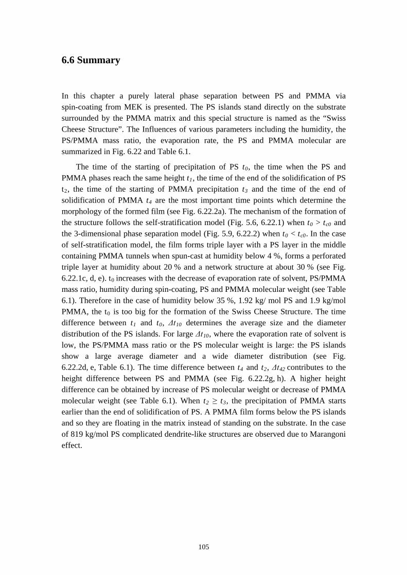
105
6.6 Summary
In this chapter a purely lateral phase separation between PS and PMMA via spin-coating from MEK is presented. The PS islands stand directly on the substrate surrounded by the PMMA matrix and this special structure is named as the “Swiss Cheese Structure”. The Influences of various parameters including the humidity, the PS/PMMA mass ratio, the evaporation rate, the PS and PMMA molecular are summarized in Fig. 6.22 and Table 6.1.
The time of the starting of precipitation of PS t0, the time when the PS and PMMA phases reach the same height t1, the time of the end of the solidification of PS t2, the time of the starting of PMMA precipitation t3 and the time of the end of solidification of PMMA t4 are the most important time points which determine the morphology of the formed film (see Fig. 6.22.2a). The mechanism of the formation of the structure follows the self-stratification model (Fig. 5.6, 6.22.1) when t0 > tc0 and the 3-dimensional phase separation model (Fig. 5.9, 6.22.2) when t0 < tc0. In the case of self-stratification model, the film forms triple layer with a PS layer in the middle containing PMMA tunnels when spun-cast at humidity below 4 %, forms a perforated triple layer at humidity about 20 % and a network structure at about 30 % (see Fig. 6.22.1c, d, e). t0 increases with the decrease of evaporation rate of solvent, PS/PMMA mass ratio, humidity during spin-coating, PS and PMMA molecular weight (see Table 6.1). Therefore in the case of humidity below 35 %, 1.92 kg/ mol PS and 1.9 kg/mol PMMA, the t0 is too big for the formation of the Swiss Cheese Structure. The time difference between t1 and t0, Δt10 determines the average size and the diameter distribution of the PS islands. For large Δt10, where the evaporation rate of solvent is low, the PS/PMMA mass ratio or the PS molecular weight is large: the PS islands show a large average diameter and a wide diameter distribution (see Fig. 6.22.2d, e, Table 6.1). The time difference between t4 and t2, Δt42 contributes to the height difference between PS and PMMA (see Fig. 6.22.2g, h). A higher height difference can be obtained by increase of PS molecular weight or decrease of PMMA molecular weight (see Table 6.1). When t2 ≥ t3, the precipitation of PMMA starts earlier than the end of solidification of PS. A PMMA film forms below the PS islands and so they are floating in the matrix instead of standing on the substrate. In the case of 819 kg/mol PS complicated dendrite-like structures are observed due to Marangoni effect.
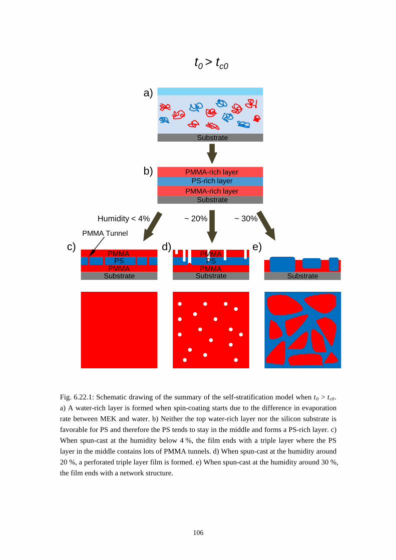
106
Fig. 6.22.1: Schematic drawing of the summary of the self-stratification model when t0 > tc0
. a) A water-rich layer is formed when spin-coating starts due to the difference in evaporation rate between MEK and water. b) Neither the top water-rich layer nor the silicon substrate is favorable for PS and therefore the PS tends to stay in the middle and forms a PS-rich layer. c) When spun-cast at the humidity below 4 %, the film ends with a triple layer where the PS layer in the middle contains lots of PMMA tunnels. d) When spun-cast at the humidity around 20 %, a perforated triple layer film is formed. e) When spun-cast at the humidity around 30 %, the film ends with a network structure.
SubstratePMMA-rich layer
PMMA-rich layerPS-rich layer
Substrate
Substrate
PSPMMA
PMMA
PMMA Tunnel
SubstratePMMA
PMMAPS
Substrate
Humidity < 4% ~ 20% ~ 30%
a)
b)
c) d) e)
t0 > tc0
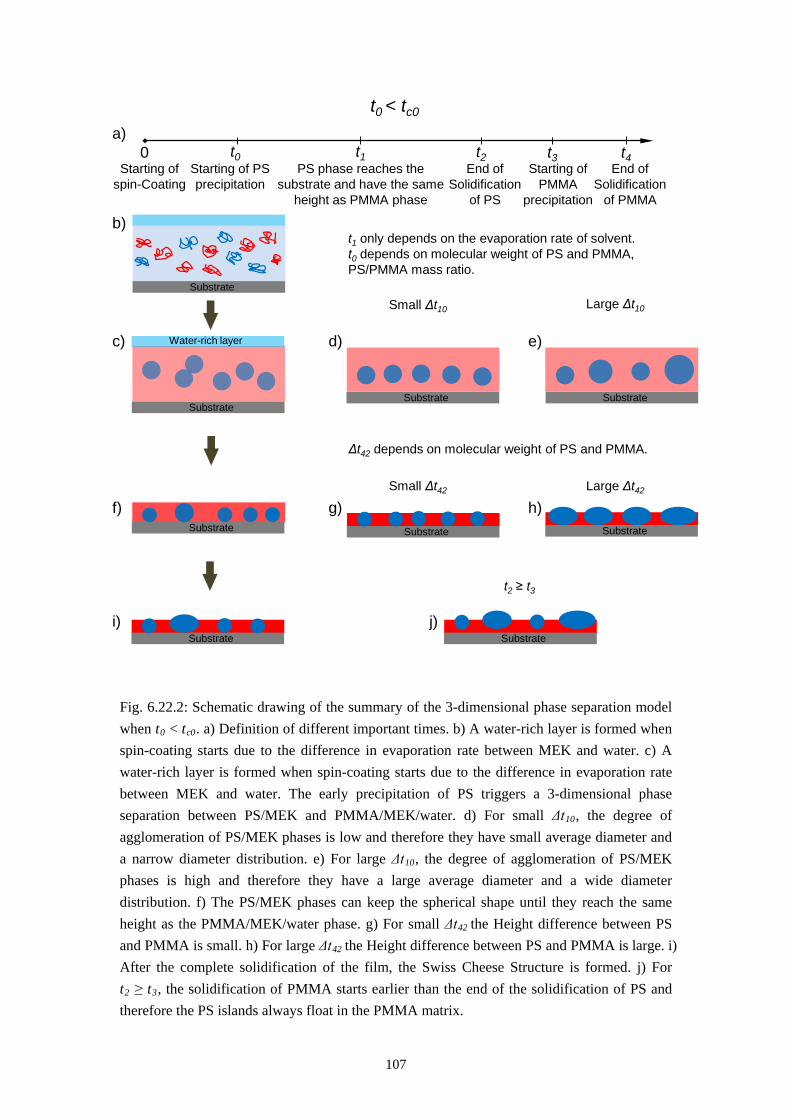
107
Fig. 6.22.2: Schematic drawing of the summary of the 3-dimensional phase separation model when t0 < tc0. a) Definition of different important times. b) A water-rich layer is formed when spin-coating starts due to the difference in evaporation rate between MEK and water. c) A water-rich layer is formed when spin-coating starts due to the difference in evaporation rate between MEK and water. The early precipitation of PS triggers a 3-dimensional phase separation between PS/MEK and PMMA/MEK/water. d) For small Δt10, the degree of agglomeration of PS/MEK phases is low and therefore they have small average diameter and a narrow diameter distribution. e) For large Δt10, the degree of agglomeration of PS/MEK phases is high and therefore they have a large average diameter and a wide diameter distribution. f) The PS/MEK phases can keep the spherical shape until they reach the same height as the PMMA/MEK/water phase. g) For small Δt42 the Height difference between PS and PMMA is small. h) For large Δt42 the Height difference between PS and PMMA is large. i) After the complete solidification of the film, the Swiss Cheese Structure is formed. j) For t2 ≥ t3
Substrate
Substrate
Water-rich layer
Substrate
Substrate
Substrate
t00 t1 t4Starting of
spin-CoatingStarting of PS precipitation
PS phase reaches the substrate and have the same
height as PMMA phase
End of Solidification
of PMMA
t2End of
Solidification of PS
Substrate
t1 only depends on the evaporation rate of solvent.t0 depends on molecular weight of PS and PMMA, PS/PMMA mass ratio.
Small Δt10 Large Δt10
Substrate Substrate
Δt42 depends on molecular weight of PS and PMMA.
Small Δt42 Large Δt42
Substrate
t2 ≥ t3
t3Starting of
PMMA precipitation
t0 < tc0
a)
b)
c) d) e)
f) g) h)
i) j)
, the solidification of PMMA starts earlier than the end of the solidification of PS and therefore the PS islands always float in the PMMA matrix.
108
Table 6.1: Influences of various parameters on the morphology of the Swiss Cheese Structure.
Increase of
A B C D E
Evaporation
rate of
solvent
PS/PMMA
Mass
Ratio
PS
Molecular
Weight
PMMA
Molecular
Weight
Humidity
t decrease 0 decrease decrease decrease decrease
t - 3 - - decrease decrease
Δt decrease 10 increase increase - -
Δt - 42 - increase decrease -
PS Islands Average Size
decrease increase increase - -
PS Islands Size
Distribution decrease increase increase - -
PS/PMMA Height
Difference - increase increase - -
A. Fast evaporation will decrease the duration of the whole spin-coating procedure and thus ends with an earlier precipitation of PS, shorter Δt10
B. The more PS in the system, the earlier the precipitation starts and the larger the Δt
, consequently a small PS islands average diameter and a narrow diameter distribution.
10
C. High PS molecular weight decreases its miscibility with water/MEK mixture and therefore the whole drying process of PS occurs earlier, expressed in the parameters in our model a small t
, which ends with a large PS islands average diameter and a wide diameter distribution. Since the PS islands grow always three dimensionally, the PS/PMMA height difference will also increase.
0, large Δt10 and Δt42
D. High PMMA molecular weight decreases the miscibility of PS in the PS/PMMA/MEK/water system and also starts an earlier precipitation of PMMA. Therefore t
. Consequently the PS islands average diameter becomes larger, the diameter distribution wider and the PS/PMMA height difference larger.
0, t3 and Δt42 become smaller. If t3
E. Higher humidity brings more water into the solution via condensation during spin-coating and thus decreases the t
comes before the end of solidification of PS, the PS islands will float in the PMMA matrix instead of standing on the substrate.
0 and t3. The purely lateral phase separation will not occur if t0 > tc0.
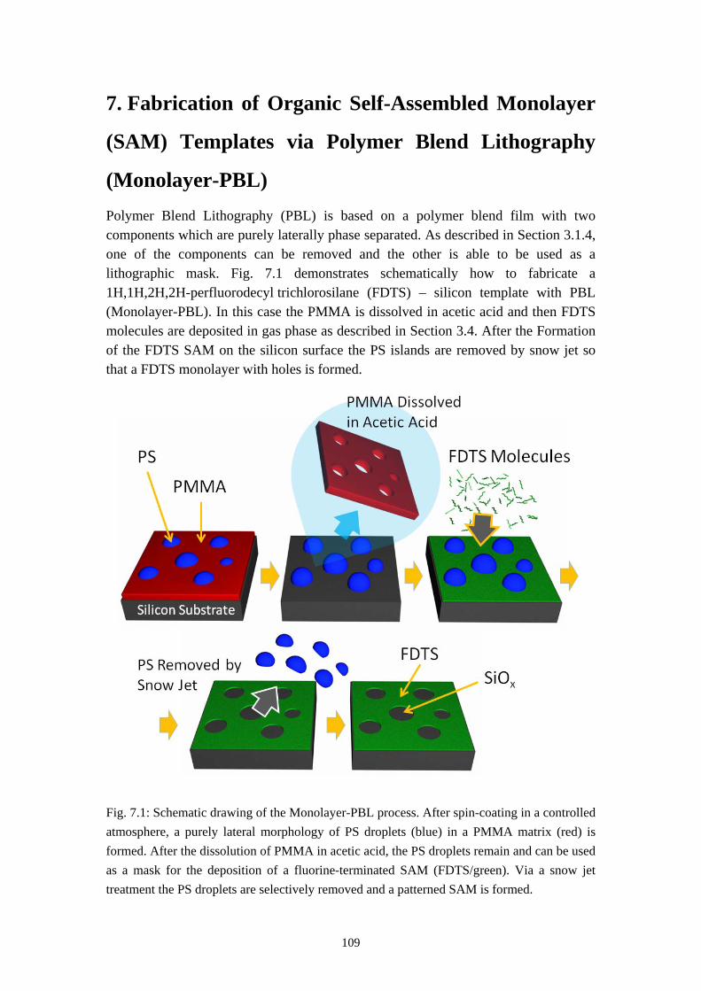
109
7. Fabrication of Organic Self-Assembled Monolayer
(SAM) Templates via Polymer Blend Lithography
(Monolayer-PBL) Polymer Blend Lithography (PBL) is based on a polymer blend film with two components which are purely laterally phase separated. As described in Section 3.1.4, one of the components can be removed and the other is able to be used as a lithographic mask. Fig. 7.1 demonstrates schematically how to fabricate a 1H,1H,2H,2H-perfluorodecyl trichlorosilane (FDTS) – silicon template with PBL (Monolayer-PBL). In this case the PMMA is dissolved in acetic acid and then FDTS molecules are deposited in gas phase as described in Section 3.4. After the Formation of the FDTS SAM on the silicon surface the PS islands are removed by snow jet so that a FDTS monolayer with holes is formed.
Fig. 7.1: Schematic drawing of the Monolayer-PBL process. After spin-coating in a controlled atmosphere, a purely lateral morphology of PS droplets (blue) in a PMMA matrix (red) is formed. After the dissolution of PMMA in acetic acid, the PS droplets remain and can be used as a mask for the deposition of a fluorine-terminated SAM (FDTS/green). Via a snow jet treatment the PS droplets are selectively removed and a patterned SAM is formed.
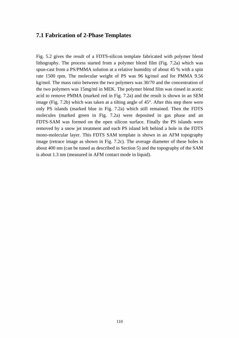
110
7.1 Fabrication of 2-Phase Templates
Fig. 5.2 gives the result of a FDTS-silicon template fabricated with polymer blend lithography. The process started from a polymer blend film (Fig. 7.2a) which was spun-cast from a PS/PMMA solution at a relative humidity of about 45 % with a spin rate 1500 rpm. The molecular weight of PS was 96 kg/mol and for PMMA 9.56 kg/mol. The mass ratio between the two polymers was 30/70 and the concentration of the two polymers was 15mg/ml in MEK. The polymer blend film was rinsed in acetic acid to remove PMMA (marked red in Fig. 7.2a) and the result is shown in an SEM image (Fig. 7.2b) which was taken at a tilting angle of 45°. After this step there were only PS islands (marked blue in Fig. 7.2a) which still remained. Then the FDTS molecules (marked green in Fig. 7.2a) were deposited in gas phase and an FDTS-SAM was formed on the open silicon surface. Finally the PS islands were removed by a snow jet treatment and each PS island left behind a hole in the FDTS mono-molecular layer. This FDTS SAM template is shown in an AFM topography image (retrace image as shown in Fig. 7.2c). The average diameter of these holes is about 400 nm (can be tuned as described in Section 5) and the topography of the SAM is about 1.3 nm (measured in AFM contact mode in liquid).
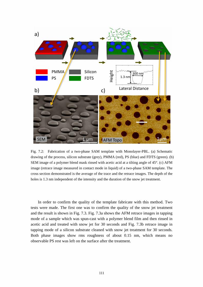
111
Fig. 7.2: Fabrication of a two-phase SAM template with Monolayer-PBL. (a) Schematic drawing of the process, silicon substrate (grey), PMMA (red), PS (blue) and FDTS (green). (b) SEM image of a polymer blend mask rinsed with acetic acid at a tilting angle of 45°. (c) AFM image (retrace image measured in contact mode in liquid) of a two-phase SAM template. The cross section demonstrated is the average of the trace and the retrace images. The depth of the holes is 1.3 nm independent of the intensity and the duration of the snow jet treatment.
In order to confirm the quality of the template fabricate with this method. Two tests were made. The first one was to confirm the quality of the snow jet treatment and the result is shown in Fig. 7.3. Fig. 7.3a shows the AFM retrace images in tapping mode of a sample which was spun-cast with a polymer blend film and then rinsed in acetic acid and treated with snow jet for 30 seconds and Fig. 7.3b retrace image in tapping mode of a silicon substrate cleaned with snow jet treatment for 30 seconds. Both phase images show rms roughness of about 0.15 nm, which means no observable PS rest was left on the surface after the treatment.
1 μm AFM Topo 1μm
c)
a)
b)
PMMAPS
SiliconFDTS
300 nm1.3 nm
SEM
Lateral Distance
Heig
ht
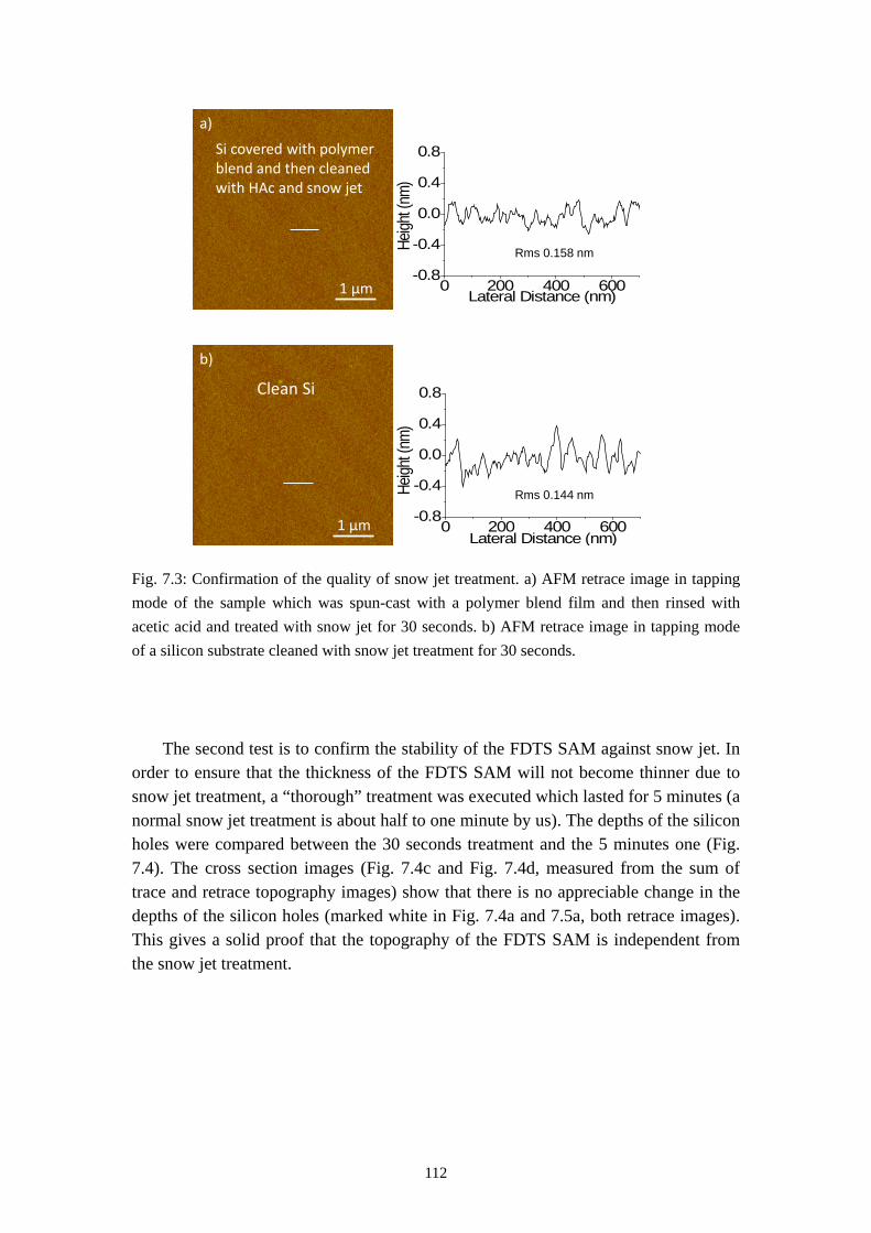
112
Fig. 7.3: Confirmation of the quality of snow jet treatment. a) AFM retrace image in tapping mode of the sample which was spun-cast with a polymer blend film and then rinsed with acetic acid and treated with snow jet for 30 seconds. b) AFM retrace image in tapping mode of a silicon substrate cleaned with snow jet treatment for 30 seconds.
The second test is to confirm the stability of the FDTS SAM against snow jet. In order to ensure that the thickness of the FDTS SAM will not become thinner due to snow jet treatment, a “thorough” treatment was executed which lasted for 5 minutes (a normal snow jet treatment is about half to one minute by us). The depths of the silicon holes were compared between the 30 seconds treatment and the 5 minutes one (Fig. 7.4). The cross section images (Fig. 7.4c and Fig. 7.4d, measured from the sum of trace and retrace topography images) show that there is no appreciable change in the depths of the silicon holes (marked white in Fig. 7.4a and 7.5a, both retrace images). This gives a solid proof that the topography of the FDTS SAM is independent from the snow jet treatment.
Si cover with polymer blend and then cleaned with HAc and snow jet
Clean Si
Height
Height
Si covered with polymer blend and then cleaned with HAc and snow jet
1 μm
Clean Si
1 μm
0 200 400 600-0.8
-0.4
0.0
0.4
0.8
Heigh
t (nm
)
Lateral Distance (nm)
Rms 0.158 nm
0 200 400 600-0.8
-0.4
0.0
0.4
0.8He
ight (
nm)
Lateral Distance (nm)
Rms 0.144 nm
a)
b)
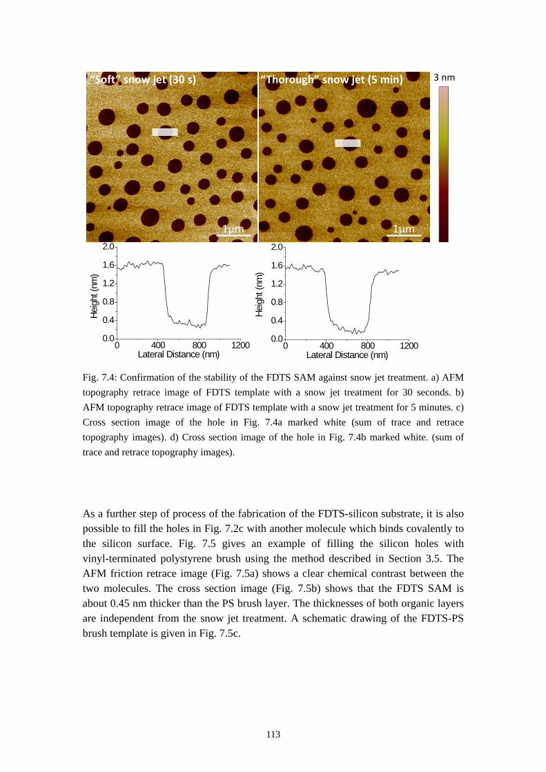
113
Fig. 7.4: Confirmation of the stability of the FDTS SAM against snow jet treatment. a) AFM topography retrace image of FDTS template with a snow jet treatment for 30 seconds. b) AFM topography retrace image of FDTS template with a snow jet treatment for 5 minutes. c) Cross section image of the hole in Fig. 7.4a marked white (sum of trace and retrace topography images). d) Cross section image of the hole in Fig. 7.4b marked white. (sum of trace and retrace topography images).
As a further step of process of the fabrication of the FDTS-silicon substrate, it is also possible to fill the holes in Fig. 7.2c with another molecule which binds covalently to the silicon surface. Fig. 7.5 gives an example of filling the silicon holes with vinyl-terminated polystyrene brush using the method described in Section 3.5. The AFM friction retrace image (Fig. 7.5a) shows a clear chemical contrast between the two molecules. The cross section image (Fig. 7.5b) shows that the FDTS SAM is about 0.45 nm thicker than the PS brush layer. The thicknesses of both organic layers are independent from the snow jet treatment. A schematic drawing of the FDTS-PS brush template is given in Fig. 7.5c.
1μm 1μm
3 nm“Soft” snow jet (30 s) “Thorough” snow jet (5 min)
0 400 800 12000.0
0.4
0.8
1.2
1.6
2.0He
ight
(nm
)
Lateral Distance (nm)0 400 800 1200
0.0
0.4
0.8
1.2
1.6
2.0
Heig
ht (n
m)
Lateral Distance (nm)
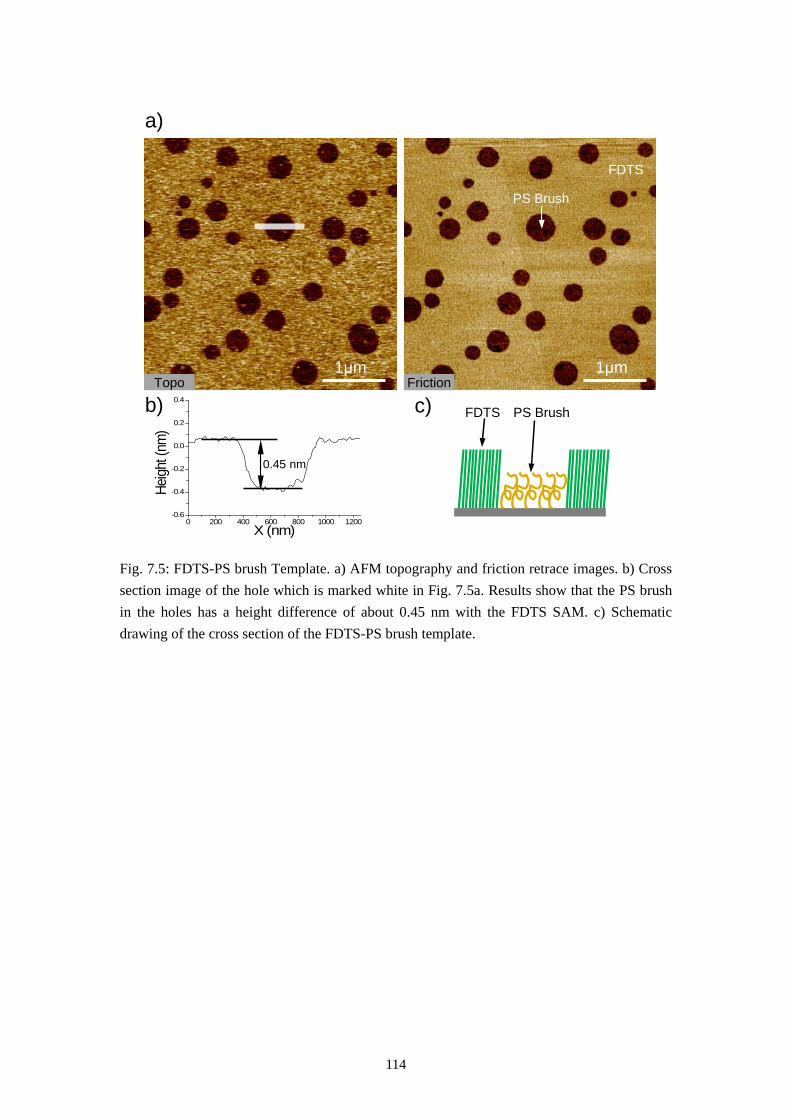
114
Fig. 7.5: FDTS-PS brush Template. a) AFM topography and friction retrace images. b) Cross section image of the hole which is marked white in Fig. 7.5a. Results show that the PS brush in the holes has a height difference of about 0.45 nm with the FDTS SAM. c) Schematic drawing of the cross section of the FDTS-PS brush template.
FDTS
Topo Friction
PS Brush
1μm 1μm
0 200 400 600 800 1000 1200-0.6
-0.4
-0.2
0.0
0.2
0.4
Heigh
t (nm
)
X (nm)
0.45 nm
a)
b) c) FDTS PS Brush
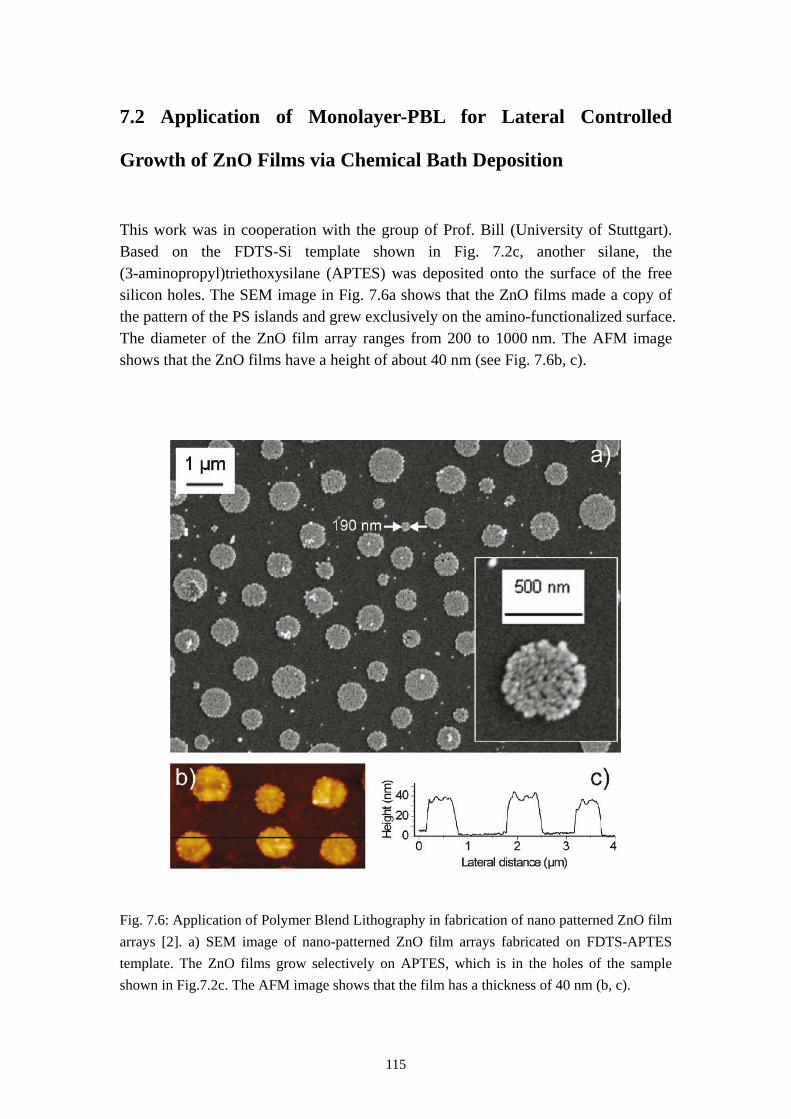
115
7.2 Application of Monolayer-PBL for Lateral Controlled
Growth of ZnO Films via Chemical Bath Deposition
This work was in cooperation with the group of Prof. Bill (University of Stuttgart). Based on the FDTS-Si template shown in Fig. 7.2c, another silane, the (3-aminopropyl)triethoxysilane (APTES) was deposited onto the surface of the free silicon holes. The SEM image in Fig. 7.6a shows that the ZnO films made a copy of the pattern of the PS islands and grew exclusively on the amino-functionalized surface. The diameter of the ZnO film array ranges from 200 to 1000 nm. The AFM image shows that the ZnO films have a height of about 40 nm (see Fig. 7.6b, c).
Fig. 7.6: Application of Polymer Blend Lithography in fabrication of nano patterned ZnO film arrays [2]. a) SEM image of nano-patterned ZnO film arrays fabricated on FDTS-APTES template. The ZnO films grow selectively on APTES, which is in the holes of the sample shown in Fig.7.2c. The AFM image shows that the film has a thickness of 40 nm (b, c).
116
7.3 Fabrication of 3-Phase Templates
When spun-cast under a range of relative humidity from 50 to 65 %, the resulting phase morphology of the polymer blend film (other conditions are exactly the same as described in Section 5.2) is different from the situation shown in Fig. 5.5.2a (45 % humidity). As can be seen in Fig. 7.7b, holes in the polymer film can be observed directly after spin-coating. Besides these open holes, there are smaller depressions and embedded PS droplets visible at the surface.
Due to the rapid evaporation of the solvent during the spin-coating process the sample-surface is cooled down. At this highly increased humidity the sample-surface reaches the dew point. The result is that water condensates and then forms droplets which leave holes in the polymer film after it is solidified. The small depressions are most likely relics of smaller water droplets which did not reach the silicon substrate. Hence, the result of the spin-coating process is a perforated PMMA layer with embedded PS droplets. This provides the opportunity to design a three-phase pattern as described below.
The (water-) holes can directly be filled with a silane monolayer. Here we used the (3-aminopropyl)triethoxysilane (APTES) molecule exposing an amino-functional group. After removing the PMMA layer with acetic acid, the CF3-terminated FDTS SAM was deposited in gas phase. Next, we removed Polystyrene by snow jet treatment as described in Section 3.1.1. The FDTS as well as the APTES SAMs withstand this cleaning procedure without any detectable change at their surface, as can be seen in Fig. 7.4. The three-phase SAM template consisting of APTES, FDTS and silicon oxide pattern elements is fabricated with topography of approximately 1.3 nm (see Fig. 7.7d). The roughness of 0.2 nm remaining in the SiOx-regions is in the same range as the one of the original Si-wafer. The height of the APTES-SAM was found to be 0.7 nm, measured in contact mode AFM in liquid. So the APTES regions look like halve-filled holes (see Fig. 7.7c).
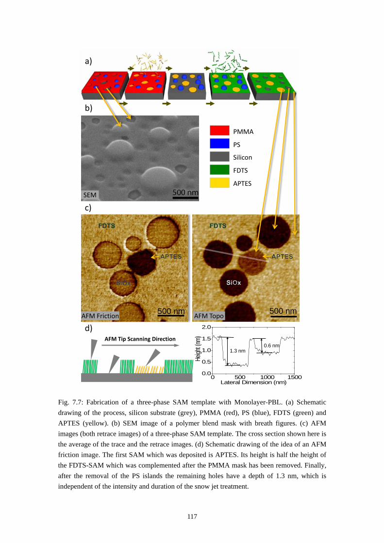
117
Fig. 7.7: Fabrication of a three-phase SAM template with Monolayer-PBL. (a) Schematic drawing of the process, silicon substrate (grey), PMMA (red), PS (blue), FDTS (green) and APTES (yellow). (b) SEM image of a polymer blend mask with breath figures. (c) AFM images (both retrace images) of a three-phase SAM template. The cross section shown here is the average of the trace and the retrace images. (d) Schematic drawing of the idea of an AFM friction image. The first SAM which was deposited is APTES. Its height is half the height of the FDTS-SAM which was complemented after the PMMA mask has been removed. Finally, after the removal of the PS islands the remaining holes have a depth of 1.3 nm, which is independent of the intensity and duration of the snow jet treatment.
b)
c)
0 500 1000 15000.0
0.5
1.0
1.5
2.0
Heigh
t (nm)
Lateral Dimension (nm)
1.3 nm0.6 nm
500 nmAFM Topo500 nmAFM Friction 500 nm
d)AFM Tip Scanning Direction
PMMA
PS
Silicon
FDTS
APTES
a)
SEM

118
119
7.4 Summary and Perspectives
Monolayer Polymer blend lithography (Monolayer-PBL) makes use of the lateral structure formation during the spin-coating process of a polymer blend film. The structures are transformed into a patterned SAM with two or three different chemical functionalities by a lift-off process. PBL starts with spin-casting a polymer blend (PS/PMMA in MEK in the study) onto a substrate (Si in the study), which forms a polymer blend film with purely lateral phase morphology. After the selective dissolution of one of the polymer components, the remaining second polymer component can be directly used as a lithographic mask. This lithographic mask, in turn, can be removed by snow jet lift-off after deposition of a silane monolayer (SAM) on the unprotected areas in the vapor phase. For the examples demonstrated, the fabricated nano-patterned template shows a chemical contrast between the functional group of the silane SAM and the bare silicon oxide. This quasi two-dimensional pattern has about 1 nm topography. The bare silicon oxide surface can be filled with another silane SAM for specific applications. The lateral structure size within the nanoscale pattern is determined by the diameter of the PS islands formed during the spin-coating process. The mean value of the statistically distributed diameters of PS islands can be varied between 90 nm and 500 nm by changing the molar mass of the PS moiety. Combined with breath figures, this lithographic method can even be used for the fabrication of three component templates. Here we use for the patterning the CF3
The quasi two-dimensional chemical patterns open potentials for their applications as templates for subsequent self-assembly of inorganic materials. Materials such as ZnO films can be assembled from chemical bath deposition [2]. The laterally heterogeneous surface could be used for constructive lithography [112, 113], laterally controlled dewetting [114], or cell adhesion studies [123]. The extreme flatness (rms roughness below 0.5 nm) allows for a highly sensitive monitoring of laterally controlled growth processes by AFM. Together with the chemical variability Polymer Blend Lithography (PBL) can become an important tool for studying surface-initiated processes.
-terminated FDTS monolayer, the amino-terminated APTES monolayer and leave at the same time uncovered regions of bare silicon oxide on the substrates.

120
121
8. Fabrication of Metals Island Arrays or Perforated
Metal Films with PBL (Metal-PBL)
8.1 Fabrication of Metal Islands or Perforated Films
The Polymer Blend Lithography method for the fabrication of metal templates (Metal-PBL) is schematically demonstrated in Figure 8.1. The process is based on the purely lateral phase separation between PS and PMMA (see Fig. 8.1a). In this work cyclohexane was used as the selective solvent for removing PS while acetic acid for removing PMMA. Via selective dissolution, either the PMMA matrix (see Fig. 8.1b, PMMA is marked in red) or the PS islands (see Fig. 8.1i, PS is marked in blue) can be kept for lithographic application. After the deposition of metal by thermal evaporation, the desired metal covers the whole surface of the sample, including the silicon surface and the polymer lithographic mask (see in Fig. 8.1c and 8.1j, metal is marked in gold for gold). Finally the snow jet lift-off method is applied to remove the polymer as well as the metal on top of it and a nano-patterned metal template, either a film with holes (see Fig. 8.1k) or islands (see Fig.8.1d), is left on the silicon substrate, which is exactly a metal copy of the selectively dissolved polymer.
Fig. 8.1e is an SEM image taken from a tilting angle of 45° of a polymer lithographic mask which is schematically shown in Fig. 8.1b (The zoom out of Fig. 8.1e is given in Fig. 8.2a). After the polymer blend film being rinsed in cyclohexane, the PS islands were dissolved and a perforated PMMA film with holes was left on the silicon substrate. The diameters of these holes range from one to several hundred nanometers. In these holes there are sometimes still very thin films of PMMA which were formed during the phase separation between the two polymers. The thicknesses of these films are too thin to affect the adhesion between the silicon substrate and the deposited metal film. The metal islands deposited into the holes are stable enough to resist the snow jet treatment which is used for the lift-off process to remove the PMMA mask. The SEM top view image of the gold islands with a thickness of 20 nm is shown in Figure 8.1f. The islands have statistically the same size as the holes in the polymer film (see Fig. 8.1e, 8.2a). The shapes of these islands are not perfectly circular as the holes in the lithographic mask, which is caused by the tearing of the metal film during the lift-off process. For the fabrication of a perforated metal film, the polymer blend must be rinsed in acetic acid instead of cyclohexane. The PMMA will be removed and a lithographic mask consists of PS islands is left on the substrate. A smooth and clean silicon surface can be seen in the SEM image taken from a tilting angle of 45°, which is the evidence for a thorough dissolution of the PMMA. The “Go Stone” like PS islands are ideal for the followed lift-off process (see Fig. 8.1g, zoom out in Fig. 8.2b). Consequently the fabricated perforated gold film (see Fig. 8.1h) has
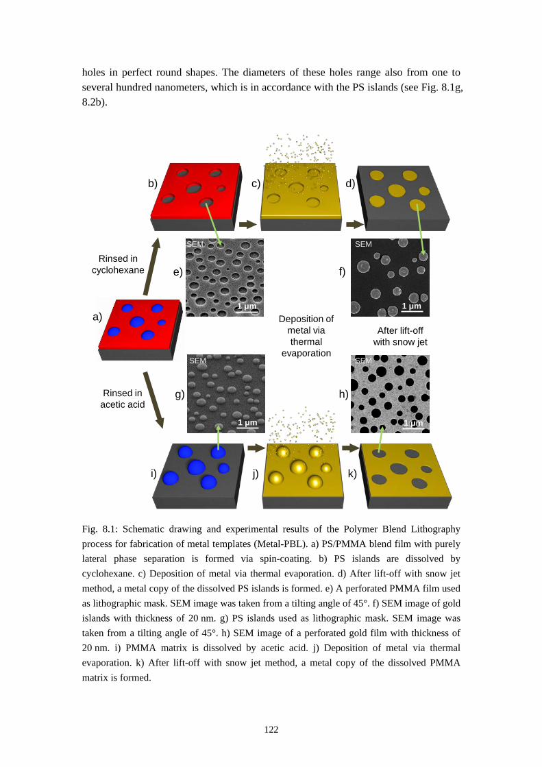
122
holes in perfect round shapes. The diameters of these holes range also from one to several hundred nanometers, which is in accordance with the PS islands (see Fig. 8.1g, 8.2b).
Fig. 8.1: Schematic drawing and experimental results of the Polymer Blend Lithography process for fabrication of metal templates (Metal-PBL). a) PS/PMMA blend film with purely lateral phase separation is formed via spin-coating. b) PS islands are dissolved by cyclohexane. c) Deposition of metal via thermal evaporation. d) After lift-off with snow jet method, a metal copy of the dissolved PS islands is formed. e) A perforated PMMA film used as lithographic mask. SEM image was taken from a tilting angle of 45°. f) SEM image of gold islands with thickness of 20 nm. g) PS islands used as lithographic mask. SEM image was taken from a tilting angle of 45°. h) SEM image of a perforated gold film with thickness of 20 nm. i) PMMA matrix is dissolved by acetic acid. j) Deposition of metal via thermal evaporation. k) After lift-off with snow jet method, a metal copy of the dissolved PMMA matrix is formed.
Rinsed in cyclohexane
Rinsed in acetic acid
Deposition of metal via thermal
evaporation
After lift-off with snow jet
a)
b) c) d)
i) j) k)
1 μm
1 μm
1 μm
1 μm
e) f)
g) h)
SEM SEM
SEMSEM
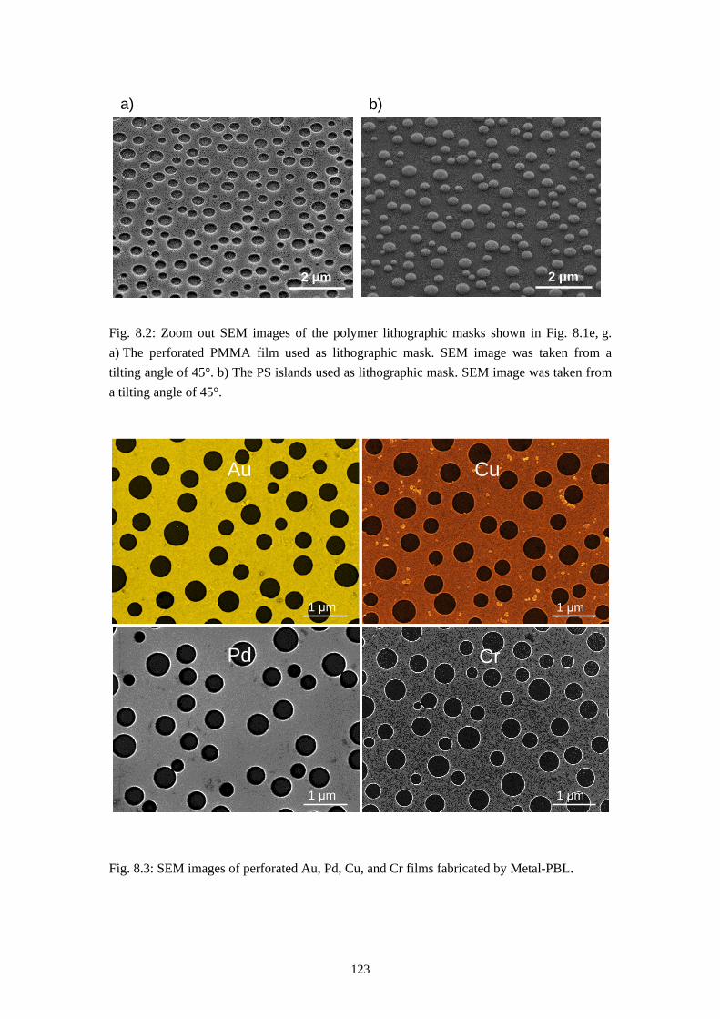
123
Fig. 8.2: Zoom out SEM images of the polymer lithographic masks shown in Fig. 8.1e, g. a) The perforated PMMA film used as lithographic mask. SEM image was taken from a tilting angle of 45°. b) The PS islands used as lithographic mask. SEM image was taken from a tilting angle of 45°.
Fig. 8.3: SEM images of perforated Au, Pd, Cu, and Cr films fabricated by Metal-PBL.
2 μm 2 μm
a) b)
1 μm
1 μm
1 μm
1 μm
Au Cu
CrPd
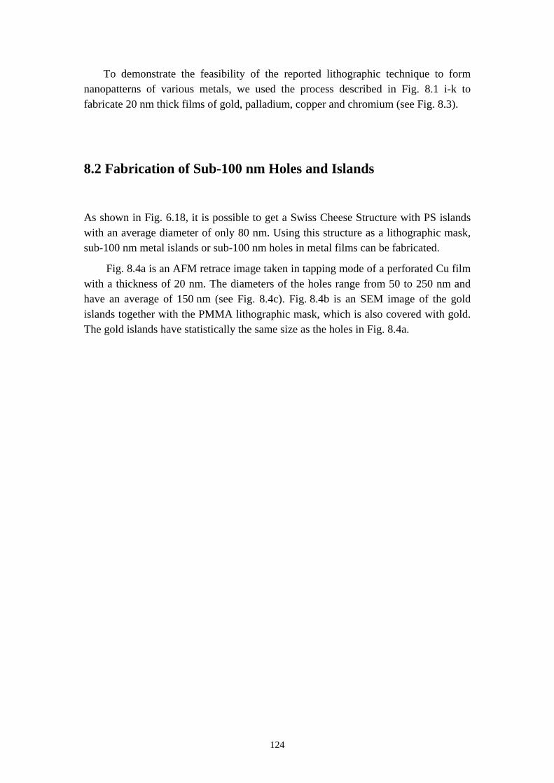
124
To demonstrate the feasibility of the reported lithographic technique to form nanopatterns of various metals, we used the process described in Fig. 8.1 i-k to fabricate 20 nm thick films of gold, palladium, copper and chromium (see Fig. 8.3).
8.2 Fabrication of Sub-100 nm Holes and Islands
As shown in Fig. 6.18, it is possible to get a Swiss Cheese Structure with PS islands with an average diameter of only 80 nm. Using this structure as a lithographic mask, sub-100 nm metal islands or sub-100 nm holes in metal films can be fabricated.
Fig. 8.4a is an AFM retrace image taken in tapping mode of a perforated Cu film with a thickness of 20 nm. The diameters of the holes range from 50 to 250 nm and have an average of 150 nm (see Fig. 8.4c). Fig. 8.4b is an SEM image of the gold islands together with the PMMA lithographic mask, which is also covered with gold. The gold islands have statistically the same size as the holes in Fig. 8.4a.
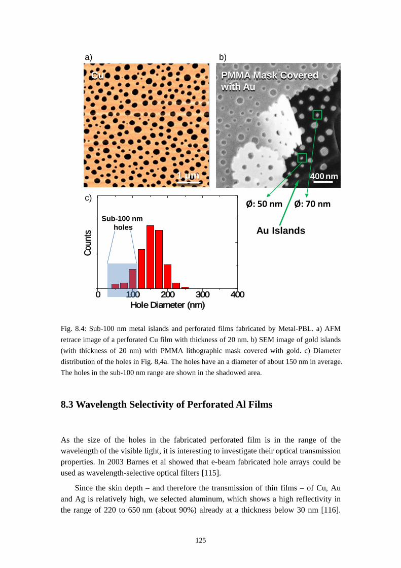
125
Fig. 8.4: Sub-100 nm metal islands and perforated films fabricated by Metal-PBL. a) AFM retrace image of a perforated Cu film with thickness of 20 nm. b) SEM image of gold islands (with thickness of 20 nm) with PMMA lithographic mask covered with gold. c) Diameter distribution of the holes in Fig. 8,4a. The holes have an a diameter of about 150 nm in average. The holes in the sub-100 nm range are shown in the shadowed area.
8.3 Wavelength Selectivity of Perforated Al Films
As the size of the holes in the fabricated perforated film is in the range of the wavelength of the visible light, it is interesting to investigate their optical transmission properties. In 2003 Barnes et al showed that e-beam fabricated hole arrays could be used as wavelength-selective optical filters [115].
Since the skin depth – and therefore the transmission of thin films – of Cu, Au and Ag is relatively high, we selected aluminum, which shows a high reflectivity in the range of 220 to 650 nm (about 90%) already at a thickness below 30 nm [116].
400nm
Ø: 70 nmØ: 50 nm
1 μm
a) b)
0 100 200 300 400
Coun
ts
Hole Diameter (nm)
c)
Sub-100 nm holes
PMMA Mask Covered with Au
Cu
Au Islands
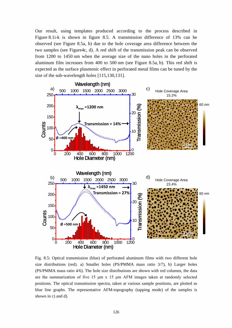
126
Our result, using templates produced according to the process described in Figure 8.1i-k is shown in figure 8.5. A transmission difference of 13% can be observed (see Figure 8.5a, b) due to the hole coverage area difference between the two samples (see Figure4c, d). A red shift of the transmission peak can be observed from 1200 to 1450 nm when the average size of the nano holes in the perforated aluminum film increases from 400 to 500 nm (see Figure 8.5a, b). This red shift is expected as the surface plasmonic effect in perforated metal films can be tuned by the size of the sub-wavelength holes [115,130,131].
Fig. 8.5: Optical transmission (blue) of perforated aluminum films with two different hole size distributions (red). a) Smaller holes (PS/PMMA mass ratio 3/7), b) Larger holes (PS/PMMA mass ratio 4/6). The hole size distributions are shown with red columns, the data are the summarization of five 15 μm x 15 μm AFM images taken at randomly selected positions. The optical transmission spectra, taken at various sample positions, are plotted as blue line graphs. The representative AFM-topography (tapping mode) of the samples is shown in c) and d).
0 200 400 600 800 1000 12000
50
100
150
200
250
Coun
ts
Hole Diameter (nm)
500 1000 1500 2000 2500 3000
0
10
20
30
Tra
nsm
issi
on (%
)
Wavelength (nm)a) c)
60 nm
3 μm
λmax =1200 nm
Ø =400 nm
Transmission = 14%
0 200 400 600 800 1000 12000
50
100
150
200
250
Coun
ts
Hole Diameter (nm)
500 1000 1500 2000 2500 3000
0
10
20
30
Tra
nsm
issi
on (%
)
Wavelength (nm)b) d)
60 nm
λmax =1450 nm
Ø =500 nm
Transmission = 27%
3 μm
Hole Coverage Area15.2%
Hole Coverage Area23.4%
127
8.4 Summary and Perspectives
Metal-PBL is a rapid, easy but promising method for fabrication of micro/nanosized metal island arrays or perforated metal film in centimeter scale. PBL makes use of the purely lateral phase separation between the two immiscible polymers during spin casting. A metal copy of either of the polymer components can be achieved with the technique. PBL starts with spin-casting of a polymer blend (PS/PMMA in MEK) film onto a substrate under defined relative humidity. A purely lateral phase separation occurs at the selected adequate conditions. Either of the components can be selectively dissolved and the other used as a lithographic mask. After the anisotropic deposition of metal and the lift-off process of snow jet technique, a metal copy of the polymer contrary to the mask is achieved.
The diameter of the metal islands or the holes in the metal films can be tuned in variety of ways as described in earlier chapters. The typical diameter is from one to several hundred nanometers. By using PS with molar mass of 9.56 kg/mol, it is able to obtain nanoislands and nanoholes with diameters ranging from 50 to 200 nanometers.
The metal nanodots arrays have varieties of applications such as the localized growth of ZnO nano wires or rods [117, 118]. The surface of the metal can be selectively modified with molecules such as thiols and used for immobilization of biomaterials [119]. The perforated metal film on the other hand can be incorporated micelle lithographic technique [120,121] to implant gold dots with diameter of 10 nm into the silicon holes to form micro-nano structures for applications like cell adhesion [122, 123]. Metals like Au or Cu are also good etching resist, which can help to amplify the topographic contrast. Holes with depth of several hundred nanometers and diameters around 50 nm can help nanorods e.g. tobacco mosaic viruses to “stand” on the surface [124]. The perforated Al films, which can be fabricated on large areas based on spin-coating and physical vapor deposition (PVD), have the potential to be used as wavelength-selective optical filters. In the case of our examples they let pass NIR-light and block photons with longer wavelengths.

128
129
9. Conclusions
From Self Stratification to Purely Lateral Phase Separation
Spin-coating is a well-established technique to generate a thin polymer film on a solid substrate. In semiconductor industry and in nanotechnology it is in use to produce photo resist films (e.g. PMMA-films as resist for e-beam lithography). If a polymer blend solution instead of mono polymer solution is used, the macromolecular character and therefore the thermodynamically suppressed entropy of the polymers leads to a phase separation during the typically only one second lasting spin-coating process. The result is a lateral structure in the micron range which can be found at the surface of the polymer film. The previous studies showed that the structure formation could be controlled by the use of pre-structured substrates or can be harnessed as structure-inducing mechanism e.g. for nano porous polymer films or for the p-n interface design in polymer photovoltaic devices. Here - besides the lateral structure - the vertical self-ordering of the polymer phases plays an important role [3, 23].
In the presented work we found a new class of such a self-stratification: The spontaneous formation of a triple layer. The polymer blend solution: polystyrene and poly(methyl methacrylate) in methylethylketon forms in a dry environment (humidity below 4%) a very smooth film which consists of a PMMA film with a thin intercalated PS layer. The PS layer in the middle contains small PMMA tunnels with diameters at about 100 nm) Other PS/PMMA/solvent systems described in the literature always form double layer films with- or without a lateral structure at the air/film interface
In order to explain the formation of this complex triple layer structure, we established a model: As the commercial MEK used in the study contains a small amount of water (in our case about 0.02 %), a water-rich layer can be formed on the top due to the difference in evaporation rate between water and MEK during the spin-coating process. Neither the top water-rich layer nor the bottom hydrophilic substrate surface is favorable for the polystyrene and consequently a triple layer is formed. When the polymer blend film is spun-cast at higher humidity (about 35 %), a completely different structure is formed with the same polymer solution: A purely lateral phase separation occurs between PS and PMMA. This structure we named the “Swiss Cheese Structure”, where the PS islands standing in the PMMA matrix and both phases have contact to the substrate as well as to the air. Based on the self-stratification model, valid at low humidity, a 3-dimensional phase separation model was established for this regime: Due to the rapid evaporation of solvent a temperature drop will be induced on the substrate surface, at higher humidity water condensation starts early in the spin-coating process. The condensed water diffuses deeply into the film and accelerates the precipitation of PS and thus triggers a
130
3-dimensional phase separation between PS/MEK and PMMA/MEK/water in an earlier stage of the spin coating process. The PS-rich structures can now grow by diffusion and by droplet fusion. These spherical structures finally settle down onto the substrate. The substrate-wetting PMMA-rich phase is still liquid at this stage and partial wetting of the protruding PS droplets at both interfaces (air and substrate) is the result. When the film is completely solidified, a purely lateral morphology is formed. The time when PS starts to precipitate (t0) is crucial for the final morphology. The structure formation mechanism follows the self-stratification model (Fig. 5.6, 6.22.1) when t0 > tc0 and the 3-dimensional phase separation model (Fig. 5.9, 6.22.2) when t0 < tc0. - t0
Fig. 9.1 gives a map of the influences of the relative humidity (x), the molecular weight of PS (y), and the PS/PMMA mass ratio (z) on the final morphology (Mw of PMMA = 9.56 kg/mol, Polymer concentration = 15 mg/L, 1500 rpm) The “Swiss Cheese Zone” is the region within the triangular prism marked red where the humidity must be from 35% to 55%, the PS molecular weight from 10 to 250 kg/mol and the PS/PMMA mass ratio from 10/90 to 40/60.
increases with: 1. the decrease of evaporation rate of solvent, 2. the increase of the PS/PMMA mass ratio, 3. the PS and PMMA molecular weight and 4. with increasing humidity during spin-coating, (see Table 6.1). Therefore the “Swiss Cheese Structure” cannot be obtained at humilities below 35%, and by application of 1.92 kg/ mol PS and 1.9 kg/mol PMMA.
The average diameter and the diameter distribution can be tuned by a variety of parameters. Small average diameter and narrow diameter distribution can be achieved by increase of evaporation rate of solvent or decrease of PS/PMMA mass ratio or PS molecular weight. The minimum diameter in the range of 50-100 nm can be achieved using PS with 9.58 kg/mol..
The time-resolved reflectometry gave us information about the evaporation duration, roughness of the film and the scattering of the formed film. Since we now know about the necessary conditions for the formation of a purely lateral structure, we could transfer this to another Polymer/Polymer/Solvent System: The “Swiss Cheese Structure” can also be obtained when PMMA is replaced by PVP, a polymer with high polarity, which is also soluble in MEK.
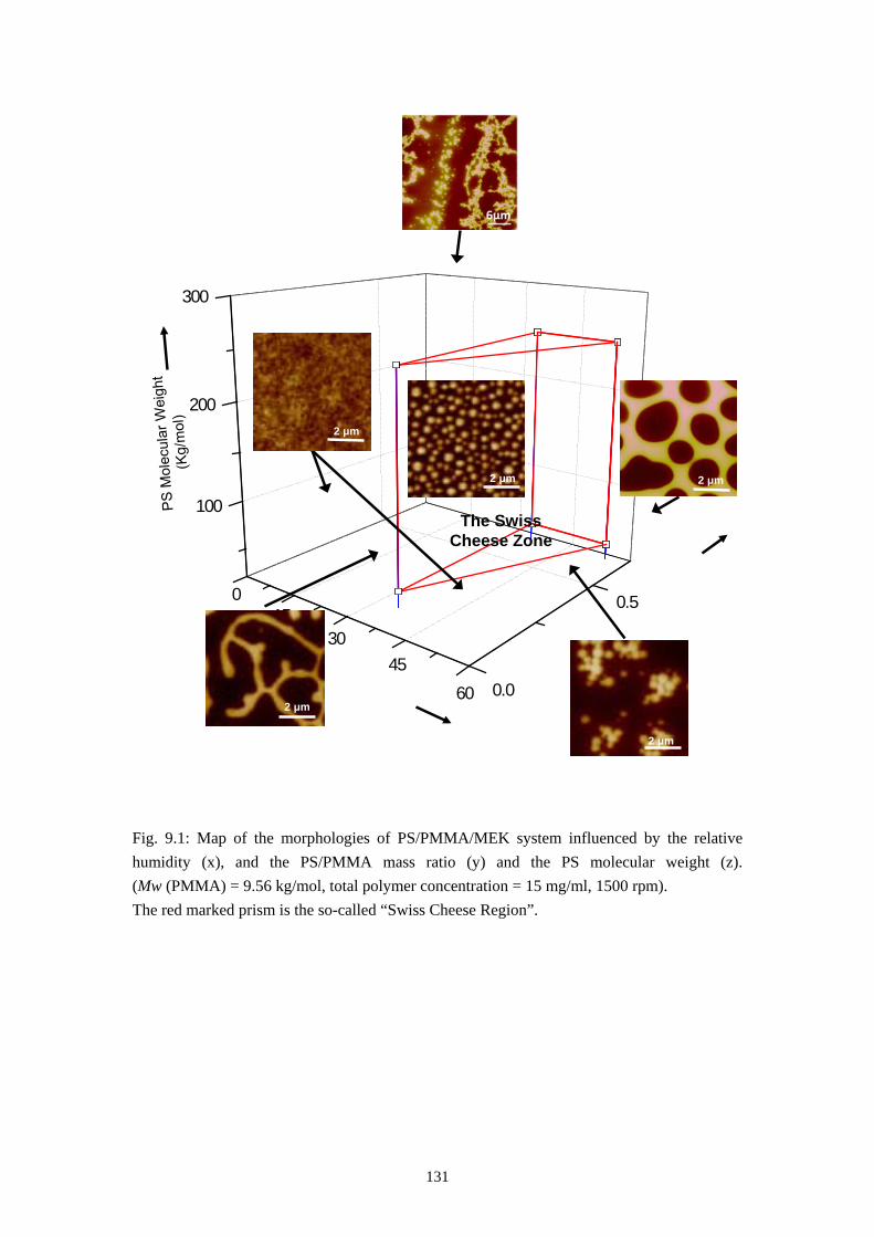
131
Fig. 9.1: Map of the morphologies of PS/PMMA/MEK system influenced by the relative humidity (x), and the PS/PMMA mass ratio (y) and the PS molecular weight (z). (Mw (PMMA) = 9.56 kg/mol, total polymer concentration = 15 mg/ml, 1500 rpm). The red marked prism is the so-called “Swiss Cheese Region”.
015
3045
60
100
200
300
0.0
0.5
2 μm
The Swiss Cheese Zone
2 μm
2 μm
2 μm
2 μm

132
133
Polymer Blend Lithography: Monolayer-PBL and Metal-PBL
Based on the “Swiss Cheese Polymer Structure”, we developed a new lithography technique, which we call Polymer Blend Lithography (PBL). PBL is a rapid, easy but promising method for the fabrication of patterned Self-Assembled Monolayers (SAMs) with two or three different chemical functionalities (Monolayer-PBL), or to produce micro/nanosized metal island arrays or perforated metal film in centimeter scale (Metal-PBL). After the selective dissolution of one of the two polymer components, the remaining polymer component can be directly used as a sharp-edged lithographic mask. This lithographic mask, in turn, can be removed by snow jet lift-off after deposition of a silane monolayer (SAM) or a metal film on the unprotected areas. The lateral structure size is determined by the diameter of the PS islands formed during the spin coating process, which can be varied in a wide range as shown in Chapter 6.
For the examples of the patterned silane SAM demonstrated in the study, the fabricated nano-patterned template shows a chemical contrast between the functional group of the silane SAM and the bare silicon oxide. This quasi two-dimensional pattern has only about 1 nanometer topography. The bare silicon oxide surface can be filled with another silane SAM for specific applications. At high humidity (over 50%) the excessive condensation of water leads to additional holes in the film, which stem from repelled water droplets which can penetrate into the viscous polymer film in the end stage of its solidification (breath figures). Using this breath figures, our lithographic method can produce even more complex three component lateral structures. (In Chapter 8 we demonstrate the possibility of making metal copies of the morphology of either PS or PMMA and thus form metal island arrays or perforated metal films. By using PS with a molar mass of 9.56 kg/mol for this metal-PBL it is possible to obtain metal nanoislands and metal films with nanoholes with diameters ranging from 50 to 250 nanometers.
In the meantime we have shown, that PBL can be used for the templated growth of inorganic and organic materials [1, 2] or even protein layers and the formation of metallic nanostructures [129], which can be used for plasmonic applications e.g. for Surface-Enhanced Raman Scattering [128].

134
135
References
[1] C. Huang, M. Moosmann, J. Jin, T. Heiler, S. Walheim and T. Schimmel: Polymer blend lithography: A Versatile Method to Fabricate Nanopatterned Self-Assembled Monolayers, Beilstein J. Nanotechnol. 2012, 3, 620.
[2] L. P. Bauermann, P. Gerstel, J. Bill, S. Walheim, C. Huang, J. Pfeifer and T. Schimmel: Templated Self-Assembly of ZnO Films on Monolayer Patterns with Nanoscale Resolution, Langmuir 2010, 26, 3744.
[3] S. Walheim, M. Boeltau, J. Mlynek, G. Krausch, and U. Steiner: Structure Formation via Polymer Demixing in Spin-Cast Films, Macromolecules 1997, 30, 4995.
[4] K. Tanaka, A. Takahara and T. Kajiyama: Film Thickness Dependence of the Surface Structure of Immiscible Polystyrene/Poly(methyl methacrylate) Blends, Macromolecules 1996, 29, 3232.
[5] J. Genzer and E. J. Kramer: Wetting of Substrates with Phase-Separated Binary Polymer Mixtures, Phys. Rev. Lett. 1997, 78 (26), 4946.
[6] P. Mansky, Y. Liu, T. P. Russell and C. Hauker: Controlling Polymer-Surface Interactions with Random Copolymer Brushes, Science 1997, 275, 1458-1460.
[7] G. Reiter: Dewetting of Thin Polymer Films, Phys. Rev. Lett. 1992, 68, 75.
[8] G. Reiter: Unstable Thin Polymer Films: Rupture and Dewetting Processes, Langmuir 1993, 9, 1344.
[9] K. Kargupta and A. Sharma: Templating of Thin Films Induced by Dewetting on Patterned Surfaces, Phys. Rev. Lett. 2001, 86, 4536.
[10] A. Budkowski, A. Bernasik, P. Cyganik, J. Raczkowska, B. Penc, B. Bergues, K. Kowalski, J. Rysz, and J. Janik: Substrate-Determined Shape of Free Surface Profiles in Spin-Cast Polymer Blend Films, Macromolecules 2003, 36, 4060.
[11] J. Jaczewska, A. Budkowski, A. Bernasik, I. Raptis, J. Raczkowska, D. Goustouridis, J. Rysz and M. Sanopoulou: Humidity and Solvent Effects in Spin-Coated Polythiophene–Polystyrene Blends, J. Appl. Polym. Sci. 2007, 105, 67.
[12] C. J. Lawrence: The Mechanics of Spin-coating of Polymer Films, J. Phys Fluids 1998, 31, 2786.
[13] J. S. Gutmann, P. Müller-Buschbaum and M. Stamm: Complex Pattern Formation by Phase Separation of Polymer Blends in Thin Films, M. Faraday Discuss 1999, 112, 258.
[14] C. Ton-That, A.G. Shard and R.H. Bradley: Surface Feature Size of Spin Cast PS/PMMA Blends, Polymer 2002, 43, 4973.
136
[15] M. Sprenger, S. Walheim, A. Budkowski and U. Steiner: Hierarchic Structure Formation in Binary and Ternary Polymer Blends, Interface Sci. 2003, 11, 225.
[16] J. Raczkowska, A. Bernasik, A. Budkowski, K. Sajewicz, B. Penc,. Lekki, M. Lekka, J. Rysz, K. Kowalski and P. Czuba: Structures Formed in Spin-Cast Films of Polystyrene Blends with Poly(butyl methacrylate) Isomers, Macromolecules 2004, 37, 7308.
[17] P. C. Jukes, S. Y. Heriot, J. S. Sharp and R. A. L. Jones: Time-Resolved Light Scattering Studies of Phase Separation in Thin Film Semiconducting Polymer Blends during Spin-Coating, Macromolecules 2005, 38, 2030.
[18] S.Y. Heriot and R. A. L. Jones: An Interfacial Instability in a Transient Wetting Layer Leads to Lateral Phase Separation in Thin Spin-Cast Polymer-Blend Films, Nat. Mater. 2005, 4, 782.
[19] G. Krausch: Surface Induced Self Assembly in Thin Polymer Films, Mater. Sci. Eng. R. 1995, 14, 1.
[20] K. Binder: Phase-Transitions in Polymer Blends and Block-copolymer Melts - Some Recent Developments, Adv. Polym. Sci. 1999, 138, 1.
[21] A. Budkowski: Interfacial Phenomena in Thin Polymer Films: Phase Coexistence and Segregation, Adv. Polym. Sci. 1999, 148, 1.
[22] P. Mokarian-Tabari, M. Geoghegan, J. R. Howse, S. Y. Heriot1, R. L. Thompson and R. A. L. Jones: Quantitative Evaluation of Evaporation Rate during Spin-Coating of Polymer Blend Films: Control of Film Structure through Defined-Atmosphere Solvent-Casting, Eur. Phys. J. E 2010, 33, 283.
[23] M. Böltau, S. Walheim, J. Mlynek, G. Krausch and U. Steiner: Surface-Induced Structure Formation of Polymer Blends on Patterned Substrates, Nature 1998, 391, 877.
[24] J. Raczkowska, A. Bernasik, A. Budkowski, J. Rysz, B. Gao and M. Lieberman: Compositional Mismatch between Chemical Patterns on a Substrate and Polymer Blends Yielding Spin-Cast Films with Subpattern Periodicity, Macromolecules 2007, 40, 2120.
[25] P. Andrew and W. T.S. Huck: Polymer Phase Separation on Lattice Patterned Surfaces, Soft Matter 2007, 3, 230.
[26] L. Cui, Z. Zhang, X. Li and Y. Han: Surface-induced Phase Separation of Binary Polymer Blends on the Chemically Patterned Substrate, Polym. Bull. 2005, 55, 131.
[27] S. Walheim, E. Schäffer, J. Mlynek and U. Steiner: Nanophase-Separated Polymer Films as High-Performance Antireflection Coatings, Science 1999, 283, 520.
[28] L. Cheng, Z. Xu, Z. Hong and Y. Yang: Interface Investigation and Engineering – Achieving High Performance Polymer Photovoltaic Devices, J. Mater. Chem. 2010, 20, 2575.
137
[29] B. Schmidt-Hansberg, M. F. G. Klein, K. Peters, F. Buss, J. Pfeifer, S. Walheim, A. Colsmann, U. Lemmer, P. Scharfer and W. Schabel: In Situ Monitoring the Drying Kinetics of Knife Coated Polymer-Fullerene Films for Organic Solar Cells, J. Appl. Phys. 2009, 106, 124501.
[30] K. Yim, W. J. Doherty, W. R. Salaneck, C. E. Murphy, R. H. Friend and J. Kim: Phase-Separated Thin Film Structures for Efficient Polymer Blend Light-Emitting Diodes, Nano Lett. 2010, 10, 385.
[31] A.Köhnen, N. Riegel, D. C. Müller and K. Meerholz: Surface-Initiated Phase Separation–Fabrication of Two-Layer Organic Light-Emitting Devices in a Single Processing Step, Adv. Mater. 2011, 23, 4301.
[32] B. Schmidt-Hansberg, M. Baunach, J. Krenn, S. Walheim, U. Lemmer, P. Scharfer and W. Schabel: Spatially Resolved Drying Kinetics of Multi-Component Solution Cast Films for Organic Electronics, Chem. Eng. Proc. 2011, 50, 509.
[33] M. Geoghegan and G. Krausch: Wetting at Polymer Surfaces and Interfaces, Prog. Polym. Sci. 2003, 28, 261.
[34] J. Sagiv: Organized Monolayers by Adsorption. 1. Formation and Structure of Oleophobic Mixed Monolayers on Solid Surfaces, JACS 1980, 102, 92.
[35] E. Sabatani, I. Rubinstein, R. Maoz and J. Sagiv: Organized Self-Assembling Monolayers on Electrodes: Part I. Octadecyl Derivatives on Gold, J. Electroanal. Chem. Interfacial 1987, 219, 365.
[36] A. Ulman: Formation and Structure of Self-Assembled Monolayers, Chem. Rev. 1996, 96, 1533.
[37] A. Zeira, J. Berson, I. Feldman, R. Maoz and J. Sagiv: A Bipolar Electrochemical Approach to Constructive Lithography: Metal/Monolayer Patterns via Consecutive Site-Defined Oxidation and Reduction, Langmuir 2011, 27, 8562.
[38] A. Gölzhäuser, W. Eck, W. Geyer, V. Stadler, T. Weimann, P. Hinze and M. Grunze: Chemical Nanolithography with Electron Beams, Adv. Mater. 2001, 13, 803.
[39] Z. She, A. DiFalco, G. Hähner and M. Buck: Electron-Beam Patterned Self-Assembled Monolayers as Templates for Cu Electrodeposition and Lift-Off, Beilstein J. Nanotechnol. 2012, 3, 101.
[40] S. Xu and G. Y. Liu: Nanometer-Scale Fabrication by Simultaneous Nanoshaving and Molecular Self-Assembly, Langmuir 1997, 13, 127.
[41] R. D. Piner, J. Zhu, F. Xu, S. Hong and C. A. Mirkin: "Dip-Pen" Nanolithography, Science 1999, 283, 661.
[42] K. Salaita, Y. Wang and C. A. Mirkin: Applications of Dip-Pen Nanolithography, Nat. Nanotechnol. 2007, 2, 145.
138
[43] E. Gnecco: A Collisional Model for AFM Manipulation of Rigid Nanoparticles, Beilstein J. Nanotechnol. 2010, 1, 158.
[44] R. Garcia, R. V. Martinez and J. Martinez: Nano-Chemistry and Scanning Probe Nanolithographies, Chen. Soc. Rev. 2006, 35, 29.
[45] S. Darwich, K. Mougin, A. Rao, E. Gnecco, S. Jayaraman and H. Haidara: Manipulation of Gold Colloidal Nanoparticles with Atomic Force Microscopy in Dynamic Mode: Influence of Particle–Substrate Chemistry and Morphology, and of Operating Conditions, Beilstein J. Nanotechnol. 2011, 2, 85.
[46] C. Obermair, A. Wagner and T. Schimmel: The Atomic Force Microscope as a Mechano–Electrochemical Pen, Beilstein J. Nanotechnol. 2011, 2, 659.
[47] F. Sun, W. P. Cai, Y. Li, B. Cao, F. Lu, G. Duan and L. Zhang: Morphology Control and Transferability of Ordered Through-Pore Arrays Based on the Electrodeposition of a Colloidal Monolayer, Adv. Mater. 2004, 16, 1116.
[48] M. R. Gonçalves, T. Makaryan, F. Enderle, S. Wiedemann, A. Plettl, O, Marti and P. Ziemann: Plasmonic Nanostructures Fabricated Using Nanosphere-Lithography, Soft-Lithography and Plasma Etching, Beilstein J. Nanotechnol. 2011, 2, 448.
[49] U. Herr, B. Kuerbanjiang, C. Benel, G. Papageorgiou, M. Goncalves, J. Boneberg, P. Leiderer, P. Ziemann, P. Marek and H. Hahn: Near-Field Effects and Energy Transfer in Hybrid Metal-Oxide Nanostructures, Beilstein J. Nanotechnol. 2013, 4, 306.
[50] S. Riedel, M. Schmotz, P. Leiderer amd J. Boneberg: Nanostructuring of Thin Films by ns Pulsed Laser Interference, J. Appl. Phys. A 2010, 101, 309.
[51] D. S. Kim, R. Ji, H. J. Fan, F. Bertram, R. Scholz, A. Dadgar, K. Nielsch, A. Krost, J. Christen, Ul. Gösele and M. Zacharias: Laser-Interference Lithography Tailored for Highly Symmetrically Arranged ZnO Nanowire Arrays, Small 2007, 3, 76.
[52] B. W. Maynor, Y. Li, and J. Liu: Au “Ink” for AFM “Dip-Pen” Nanolithography, Langmuir 2001, 17, 2575.
[53] D.I. Bower: An Introduction to Polymer Physics, Cambridge University Press, 2002.
[54] M. D. Lechner and K. Gehrke: Makromolekulare Chemie. s.l., Birkhäuser, 2010.
[55] S. Walheim: Micrometer and Sub-Micrometer Structure Formation of Phase Separating Polymer Film, Universität Konstanz, 2000. PhD dissertation
[56] S. Walheim: Phasenseparation in dünnen Polymerfilmen, Universität Konstanz, 1997. Diplomarbeit
[57] G. R. Strobl: The Physics of Polymers, Second Edition, Springer-Verlag, 1996 and 1997.
[58] M. Rubinstein and R. H. Colby: Polymer Physics, Oxford University Press Inc., 2004.
139
[59] D. J. Geveke and R. P. Danner: Ternary Phase Equilibria of Polystyrene with a Second Polymer and a Solvent, J. Appl. Polym. Sci. 1993, 47, 565.
[60] J. Jaczewska, A. Budkowski, A. Bernasik, I. Raptis, E. Moons, D. Goustouridis, J. Haberko and J. Rysz: Ordering Domains of Spin Cast Blends of Conjugated and Dielectric Polymers on Surfaces Patterned by Soft- and Photo-lithography, Soft Matter. 2009, 5, 234.
[61] F. Schreiber: Structure and Growth of Self-Assembling Monolayers, Prog. Surf. Sci. 2000, 65, 151.
[62] F. Cecchet, A. Duwez, C. Jérôme S. Gabriel, R. Jérôme, K. Glinel, S. Demoustier-Champagne, A. M. Jonas, and B. Nysten: Atomic Force Microscopy Investigation of the Morphology and the Biological Activity of Protein-Modified Surfaces for Bio- and Immunosensors, Anal. Chem. 2007, 79, 6488.
[63] A. Kumar and G. M. Whitesides: Features of Gold Having Micrometer to Centimeter Dimensions can be Formed through a Combination of Stamping with an Elastomeric Stamp and an Alkanethiol “ink“ Followed by Chemical Etching, Appl. Phys. Lett. 1993, 63, 2002.
[64] M. Geissler, H. Schmid, A. Bietsch, B. Michel, and E. Delamarche: Defecttolerant and Directional Wet-Etch Systems for Using Monolayers as Resists, Langmuir 2002, 18, 2374.
[65] Y. Xia, X.-M. Zhao, and G. M. Whitesides: Pattern Transfer: Self-Assembled Monolayers as Ultrathin Resists, Microelectron. Eng. 1996, 32, 255.
[66] E. Barena, C. Ocal, and M. Salmeron: Evolution of the Structure and Mechanical Stability of Self-Assembled Alkanethiol Islands on Au.111. due to Diffusion and Ripening, J. Chem. Phys. 1999, 111, 9797.
[67] H. Tobias: Nanokontaktlithographie auf Basis templatinduzierter Selbstorganisation amphiphiler Blockcopolymere, Karlsruher Institut für Technologie, 2011. PhD dissertation.
[68] B. Zhao: Polymer Brushes: Surface Immobilized Macromolecules, Prog. Polym. Sci. 2000, 25, 677.
[69] R. R. Bhat: Surface-Grafted Polymer Gradients: Formation, Characterization, and Applications. Adv. Polym. Sci. 2006, 198, 51.
[70] G. Reiter, G. Castelein, P. Hoerner, G. Riess, A. Blumen, and J.-U. Sommer: Nanometer-Scale Surface Patterns with Long-Range Order Created by Crystallisazion of Diblock Copolymers, Phys. Rev. Lett. 1999, 83, 3844.
[71] O. Prucker and J. Rühe: Polymer Layers through Self-Assembled Monolayers of Initiators, Langmuir 1998, 14, 6893.
140
[72] O. Prucker and J. Rühe: Synthesis of Poly(styrene) Monolayers Attached to High Surface Area Silica Gels through Self-Assembled Monolayers of Azo Initiators, Macromolecules 1998, 31, 592.
[73] O. Prucker and J. Rühe: Mechanism of Radical Chain Polymerizations Initiated by Azo Compounds Covalently Bound to the Surface of Spherical Particles, Macromolecules 1998, 31, 602.
[74] F. Pedrotti, L. Pedrotti, W. Bausch and H. Schmidt: Optik eine Einführung, Prentice Hall, 1996.
[75] J. M. Bennett: How to Clean Surfaces, Laser-Induced Damage in Optical Materials, Book Series: Proceedings of the Society of Photo-optical Instrumentation Engineers (SPIE) 2003, 5273, 195.
[76] R. Sherman, D. Hirt and R. Vane: Surface Cleaning with the Carbon Dioxide Snow Jet, J. Vac. Sci. Technol. A 1994, 12, 1876.
[77] R. Sherman: Carbon Dioxide Snow Cleaning, Part. Sci. Technol. 2007, 25, 37.
[78] W. Kern: Cleaning Solutions based on Hydrogen Peroxide for use in Silicon Semiconductor Technology, RCA Rev. 1970, 31, 187.
[79] T. Ohmi, M. Miyashita, M. Itano, T. Imaoka and I. Kawanabe: Dependence of Thin-Oxide Films Quality on Surface Microroughness, IEEE Trans. Electron Devices 1992, 39, 537.
[80] A. A. Busnaina, I. I. Kashkoush and G. W. Gale: An Experimental Study of Megasonic Cleaning of Silicon Wafers, J. Electrochem. Soc. 1995, 142, 2812.
[81] C. Extrand: Spin-Coating of Very Thin Polymer Films, Polym. Eng. Sci. 1994, 34, 390.
[82] B. Riedel: Substrat-Konsumierende Metall-Organische Schichten– Wachstumsverhalten und Nanolithographie, Karlsruher Institut für Technologie, 2009. PhD dissertation.
[83] J. H. Maas, M. A. Cohen Stuart, A. B. Sieval, H. Zuilhof, and E. J. R. Sudhölter: Preparation of Polystyrene Brushes by Reaction of Terminal Vinyl Groups on Silicon and Silica Surfaces, Thin Solid Films 2003, 426, 135.
[84] A. Vašíček: Optics of Thin Films, North-Holland Publishing Group, Amsterdam, 1960.
[85] H. Jaksch: Field Emission SEM for true Surface Imaging and Analysis, Mater. World 1996, 4, 583.
[86] J. I. Goldstein, A. D. Romig Jr., D. E. Newbury, C. E. Lyman, P. Echlin, C. Fiori, D. C. Joy and E. Lifshin: Scanning Electron Microscopy and X-Ray Microanalysis, Second Edition, Lenum Press, 1992.
[87] G. H. Michler: Electron Microscopy of Polymers, Springer, 2008.
141
[88] G. Binnig, H. Rohrer, Ch. Gerber and E. Weibel: Surface Studies by Scanning Tunneling Microscopy, Phys. Rev. Lett. 1982, 49, 57.
[89] G. Binnig, C. F. Quate and Ch. Gerber: Atomic Force Microscope, Phys. Rev. Lett. 1986, 56, 930.
[90] J. Wintterlin, J. Wiechers, H. Brune, Z. Gritsch, H. Höfer and R. J. Behm: Atomic-Resolution Imaging of Close-Packed Metal Surfaces by Scanning Tunneling Microscopy, Phys. Rev. Lett. 1989, 62, 59.
[91] C. Kittle: Einführung in die Festkörperphysik, 15th Edition, Oldenbourg, München, 2013.
[92] T. Heiler: Funktionnelle Muster aus selbstorganisierenden Monolagen durch Polymer-Phasenseparation, Karlsruher Institut für Technologie, 2008. Diplomarbeit.
[93] G. Bar: Scanning Force Microscopy Study of Patterned Monolayers of Alkanethiols on Gold. Importance of Tip-Sample Contact Area in Interpreting Force Modulation and Friction Force Microscopy images. Langmuir 1997, 13, 373.
[94] R. M. Overney, E. Meyer, J. Frommer and H.-JG. Güntherodt: Force Microscopy Study of Friction and Elastic Compliance of Phase-Separated Organic Thin Films, Langmuir 1994, 10, 1281.
[95] O Marti, J. Colchero and J. Mlynek: Combined Scanning Force and Friction Microscopy of Mica, Nanotechnology 1990, 1, 141.
[96] F. J. Giessibl and H. Bielefeldt: Physical Interpretation of Frequency- Modulation Atomic Force Microscopy, Phys. Rev. B 2000, 61, 9968.
[97] J. P. Cleveland, B. Anczykowski, A. E. Schmid and V. B. Elings: Energy Dissipation in Tapping-Mode Atomic Force Microscopy, Appl. Phys. Lett. 1997, 72, 2613.
[98] G. Krausch, M. Hipp, M. Böltau, O. Marti and J. Mlynek: High-Resolution Imaging of Polymer Surfaces with Chemical Sensitivity, Macromolecules 1995, 28, 260.
[99] J. Pfeifer: Oberflächenwelligkeit und zeitaufgelöste Schichtdickenmessung bei dünnen Polymerfilmen, Karlsruher Institut für Technologie, 2007. Diplomarbeit.
[100] H. G. Tompkins and W. A. McGahan: Spectroscopic Ellipsometry and Reflectometry, John Wiley & Sons Inc., 1999.
[101] G.Krausch: Surface induced self assembly in thin polymer films, Materials science and Engeneering 1995, R14, 1.
[102] G. Coulon, T.P. Russell, V.R. Deline, and P.F.Green: Surface-Induced Orientation of Symmetric, Diblock Copolymers: A Secondary Ion Mass-Spectrometry Study, Macromolecules 1989, 22, 2581.
142
[103] G. G. Silva, P. Rocha, P. Oliveira and B. Neves: Domain Size Effects on the Thermal Properties of PS/PMMA Blends, Appl. Surf. Sci. 2004, 238, 64.
[104] M. Souche and N. Clarke: Equilibrium Phases for Thin Films of Polymer Blend Solutions, Macromolecules 2010, 43, 5433.
[105] A. D. F. Dunbar, P. Mokarian-Tabari, A. J. Parnell, S. J. Martin, M. W. A. Skoda and R. A. L. Jones: A Solution Concentration Dependent Transition from Self-stratification to Lateral Phase Separation in Spin-cast PS:d-PMMA Thin Films, Eur. Phys. J. E. 2010, 31, 369.
[106] L. Fang, M. Wei, C. Barry and J. Mead: Effect of Spin Speed and Solution Concentration on the Directed Assembly of Polymer Blends, Macromolecules 2010, 43, 9747.
[107] K. Wu, S. Lu and H. Chen: Formation of Parallel Strips in Thin Films of Polystyrene/Poly(vinyl pyrrolidone) Blends via Spin-coating on Unpatterned Substrates, Langmuir 2006,. 22, 8029.
[108] J. Kim, K. Taki, S. Nagamine and M. Ohshima: Periodic Porous Stripe Patterning in a Polymer Blend Film Induced by Phase Separation during Spin-Casting, Langmuir 2008, 24, 8898.
[109] J. Kim, K. Taki and M. Ohshima: Preparation of a Unique Microporous Structure via Two Step Phase Separation in the Course of Drying a Ternary Polymer Solution, Langmuir 2007, 23, 12397.
[110] H. Gliemann, A. T. Almeida, D. F. S. Petri and T. Schimmel: Nanostructure Formation in Polymer Thin Films Influenced by Humidity, Surf. Interface Anal. 2007, 39, 1.
[111] W. Madej, A. Budkowski, J. Raczkowska and J. Rysz: Breath Figures in Polymer and Polymer Blend Films Spin-Coated in Dry and Humid Ambience, Langmuir 2008, 24, 3517.
[112] S. H. Choi and B. Zhang-Newby: Micrometer-Scaled Gradient Surfaces Generated Using Contact Printing of Octadecyltrichlorosilane, Langmuir 2004, 20, 7427.
[113] Y. Patz: Self-Assembled Monolayers and Titanium Dioxide: From Surface Patterning to Potential Applications, Beilstein J. Nanotechnol. 2011, 2, 845.
[114] C. Wu, Q. Cheng, S. Sun and B. Han: Templated Patterning of Graphene Oxide Using Self-Assembled Monolayers, Carbon 2012, 50, 1083.
[115] W. J. Barnes, A. Dereux and T. W. Ebbesen: Surface Plasmon Subwavelength Optics, Nature 2003, 424, 824.
[116] G. Hass and J. E. Waylons: J. Opt. Soc. Am. 1961, 51, 719.
[117] H. J. Fan, W. Lee, R. Hauschild, M. Alexe, G. L. Rhun, R. Scholz, A. Dadgar, K. Nielsch, H. Kalt, A. Krost, M. Zacharias and U. Gösele: Template-Assisted
143
Large-Scale Ordered Arrays of ZnO Pillars for Optical and Piezoelectric Applications, Small 2006, 2, 561.
[118] H. J. Fan, P. Serner and M. Zacharias: Semiconductor Nanowires: From Self-Organization to Patterned Growth, Small 2006, 2, 700.
[119] K. Ariga, T. Nakanishi and T. Michinobu: Immobilization of Biomaterials to Nano-Assembled Films (Self-Assembled Monolayers, Langmuir-Blodgett Films, and Layer-by-Layer Assemblies) and Their Related Functions, J. Nanosci. Nanotechnol. 2006, 6, 2278.
[120] J. P. Spatz, S. Mössmer, C. Hartmann and M. Möller: Ordered Deposition of Inorganic Clusters from Micellar Block Copolymer Films, Langmuir 2000, 16, 407.
[121] R. Glass, M. Möller and J. P. Spatz: Block Copolymer Micelle Nanolithography: Nanotechnology 2003, 14, 1153.
[122] E. A. Cavacanti-Adam, D. Aydin, V. C. Hirschfeld-Warneken and J. P. Spatz: Cell Adhesion and Response to Synthetic Nanopatterned Environments by Steering Receptor Clustering and Spatial Location, HFSP Journal 2008, 2, 276.
[123] B. Geiger, J. P. Spatz and A. D. Bershadsky: Environmental Sensing through Focal Adhesions, Nat Rev Mol Cell Biol. 2009, 10, 21.
[124] F. C. Geiger, F. J. Eber, S. Eiben, A. Müller, H. Jeske, J. P. Spatz and C. Wege: TMV Nanorods with Programmed Longitudinal Domains of Differently Addressable Coat Proteins, Nanoscale 2013, 5, 3808
[125] M. G. Lawrence: The Relationship between Relative Humidity and the Dew Point Temperature in Moist Air: A Simple Conversion and Applications, B. Am. Meteorol. Soc. 2005, 86, 225.
[126] M. Barczweski: Konstruktive Lithographie mit selbstorganisierenden metall-organischen Systemen, University of Karlsruhe, 2004, PhD Dissertation.
[127] C. M. Mahoney: Cluster Secondary Ion Mass Spectrometry of Polymers and Related Materials, Mass Spectrom. Rev. 2010, 29, 247.
[128] C. Tian, Z. Liu, J. Jin, S. Lebedkin, C. Huang, H. You, R. Liu, L. Wang, X. Song B. Ding, S. Walheim, T. Schimmel and J. Fang: Gold Mesoflower Arrays with sub-10 nm Intraparticle Gaps for Highly Sensitive and Repeatable Surface Enhanced Raman Spectroscopy, Nanotechnology 2012, 23, 165604.
[129] C. Huang, A. Förster, S. Walheim and T. Schimmel: Polymer blend lithography for metal films: large-area patterning with over 1 billion holes/inch2
[130] T. W. Ebbesen, H. J. Lezec, H. F. Ghaemi, T. Thio and P. A. Wolff: Extraordinary Optical Transmission through Sub-Wavelength Hole Arrays, Nature 1998, 391, 667.
, Beilstein J. Nanotechnol. 2015, 6, 1205.
[131] C. Genet and T. W. Ebbesen: Light in Tiny Holes, Nature 2007, 445, 39.
![Ultra-thin aluminium oxide films deposited by plasma- enhanced atomic layer deposition ... · 3 deposited by plasma-enhanced ALD, from [Al(CH 3) 3] with an O 2 plasma, as a protective](https://img.pdfslide.org/doc/110x75/611d563f261d0233ff71de6c/ultra-thin-aluminium-oxide-films-deposited-by-plasma-enhanced-atomic-layer-deposition.jpg)
![Von der Grundlagenforschung zur Produktion€¦ · 9-CuGaS2 10-CuS [ Mainz, Klenk, Lux-Steiner, Thin Solid Films 515 (2007) 5934] Schichtstapel a) Schichtstapel b) (T, S Einfluss)](https://img.pdfslide.org/doc/110x75/6061a81cdb958a492f6df7d8/von-der-grundlagenforschung-zur-produktion-9-cugas2-10-cus-mainz-klenk-lux-steiner.jpg)