Embed Size (px)
Citation preview
Produktspezifikation für AUO T315XW02 VF Im Programm von
Achtung: Dieses Dokument unterliegt nicht dem Änderungsdienst. Der Stand entspricht der Drucklegung. Bitte informieren Sie sich vor Verwendung ob die technischen Daten noch dem aktuellen Stand entsprechen. Trotz sorgfältiger Kontrolle können wir leider keine Haftung für Druckfehler oder Irrtümer übernehmen.
©Copyright AU Optronics, Inc. January, 2003 All Rights Reserved. T315XW02 VF - Specs. Ver 0 1/28 No Reproduction and Redistribution Allowed
Product Description: T315XW02 TFT-LCD PANEL
AUO Model Name: T315XW02 VF
Customer Part No/Project Name:
Customer Signature Date AUO Date
Approved By: Yu-Chieh Lin
Reviewed By: Hong Jye Hong
Prepared By: Jacky Su
©Copyright AU Optronics, Inc. January, 2003 All Rights Reserved. T315XW02 VF - Specs. ver 0 2/28 No Reproduction and Redistribution Allowed
Document Version : 0 Date : 2007/02/07
Product Specifications
31.5” WXGA Color TFT-LCD Module Model Name: T315XW02 VF
(*) Preliminary Specifications
( ) Final Specifications
©Copyright AU Optronics, Inc. January, 2003 All Rights Reserved. T315XW02 VF - Specs. ver 0 3/28 No Reproduction and Redistribution Allowed
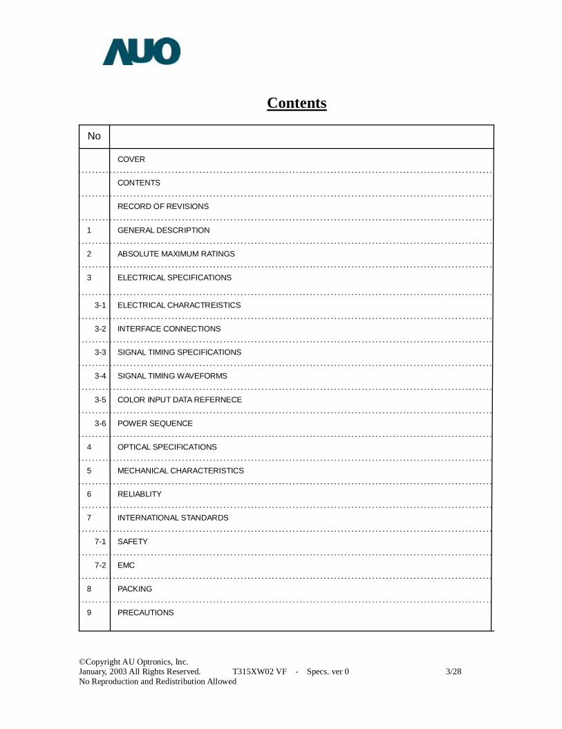
Contents
INTERFACE CONNECTIONS 3-2
COLOR INPUT DATA REFERNECE 3-5
PRECAUTIONS 9
PACKING 8
EMC 7-2
COVER
CONTENTS
RECORD OF REVISIONS
GENERAL DESCRIPTION 1
ABSOLUTE MAXIMUM RATINGS 2
ELECTRICAL SPECIFICATIONS 3
ELECTRICAL CHARACTREISTICS 3-1
SIGNAL TIMING SPECIFICATIONS 3-3
SIGNAL TIMING WAVEFORMS 3-4
POWER SEQUENCE 3-6
OPTICAL SPECIFICATIONS 4
MECHANICAL CHARACTERISTICS 5
RELIABLITY 6
INTERNATIONAL STANDARDS 7
SAFETY 7-1
No
©Copyright AU Optronics, Inc. January, 2003 All Rights Reserved. T315XW02 VF - Specs. ver 0 4/28 No Reproduction and Redistribution Allowed
Record of Revision Version Date No Old Description New Description Remark
0 2007/02/07 First issue
©Copyright AU Optronics, Inc. January, 2003 All Rights Reserved. T315XW02 VF - Specs. ver 0 5/28 No Reproduction and Redistribution Allowed
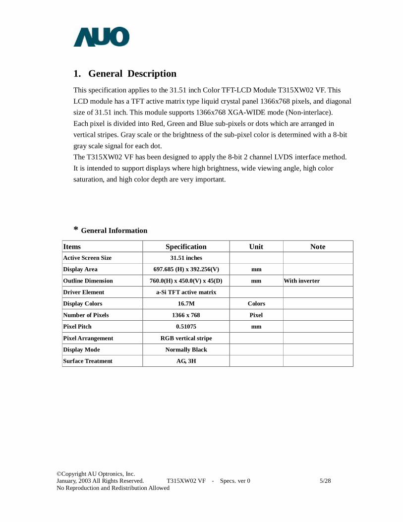
1. General Description This specification applies to the 31.51 inch Color TFT-LCD Module T315XW02 VF. This LCD module has a TFT active matrix type liquid crystal panel 1366x768 pixels, and diagonal size of 31.51 inch. This module supports 1366x768 XGA-WIDE mode (Non-interlace). Each pixel is divided into Red, Green and Blue sub-pixels or dots which are arranged in vertical stripes. Gray scale or the brightness of the sub-pixel color is determined with a 8-bit gray scale signal for each dot. The T315XW02 VF has been designed to apply the 8-bit 2 channel LVDS interface method. It is intended to support displays where high brightness, wide viewing angle, high color saturation, and high color depth are very important.
* General Information
Items Specification Unit Note Active Screen Size 31.51 inches
Display Area 697.685 (H) x 392.256(V) mm
Outline Dimension 760.0(H) x 450.0(V) x 45(D) mm With inverter
Driver Element a-Si TFT active matrix
Display Colors 16.7M Colors
Number of Pixels 1366 x 768 Pixel
Pixel Pitch 0.51075 mm
Pixel Arrangement RGB vertical stripe
Display Mode Normally Black
Surface Treatment AG, 3H
©Copyright AU Optronics, Inc. January, 2003 All Rights Reserved. T315XW02 VF - Specs. ver 0 6/28 No Reproduction and Redistribution Allowed
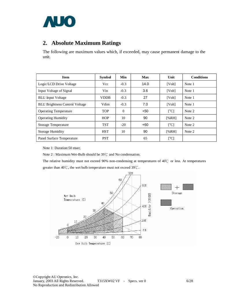
2. Absolute Maximum Ratings The following are maximum values which, if exceeded, may cause permanent damage to the unit.
Item Symbol Min Max Unit Conditions
Logic/LCD Drive Voltage Vcc -0.3 14.0 [Volt] Note 1
Input Voltage of Signal Vin -0.3 3.6 [Volt] Note 1
BLU Input Voltage VDDB -0.3 27 [Volt] Note 1
BLU Brightness Control Voltage Vdim -0.3 7.0 [Volt] Note 1
Operating Temperature TOP 0 +50 [oC] Note 2
Operating Humidity HOP 10 90 [%RH] Note 2
Storage Temperature TST -20 +60 [oC] Note 2
Storage Humidity HST 10 90 [%RH] Note 2
Panel Surface Temperature PST 65 [oC]
Note 1: Duration:50 msec.
Note 2 : Maximum Wet-Bulb should be 39 and No condensation.℃
The relative humidity must not exceed 90% non-condensing at temperatures of 40 or less. At temperatures ℃
greater than 40 , the wet b℃ ulb temperature must not exceed 39 . ℃
©Copyright AU Optronics, Inc. January, 2003 All Rights Reserved. T315XW02 VF - Specs. ver 0 7/28 No Reproduction and Redistribution Allowed
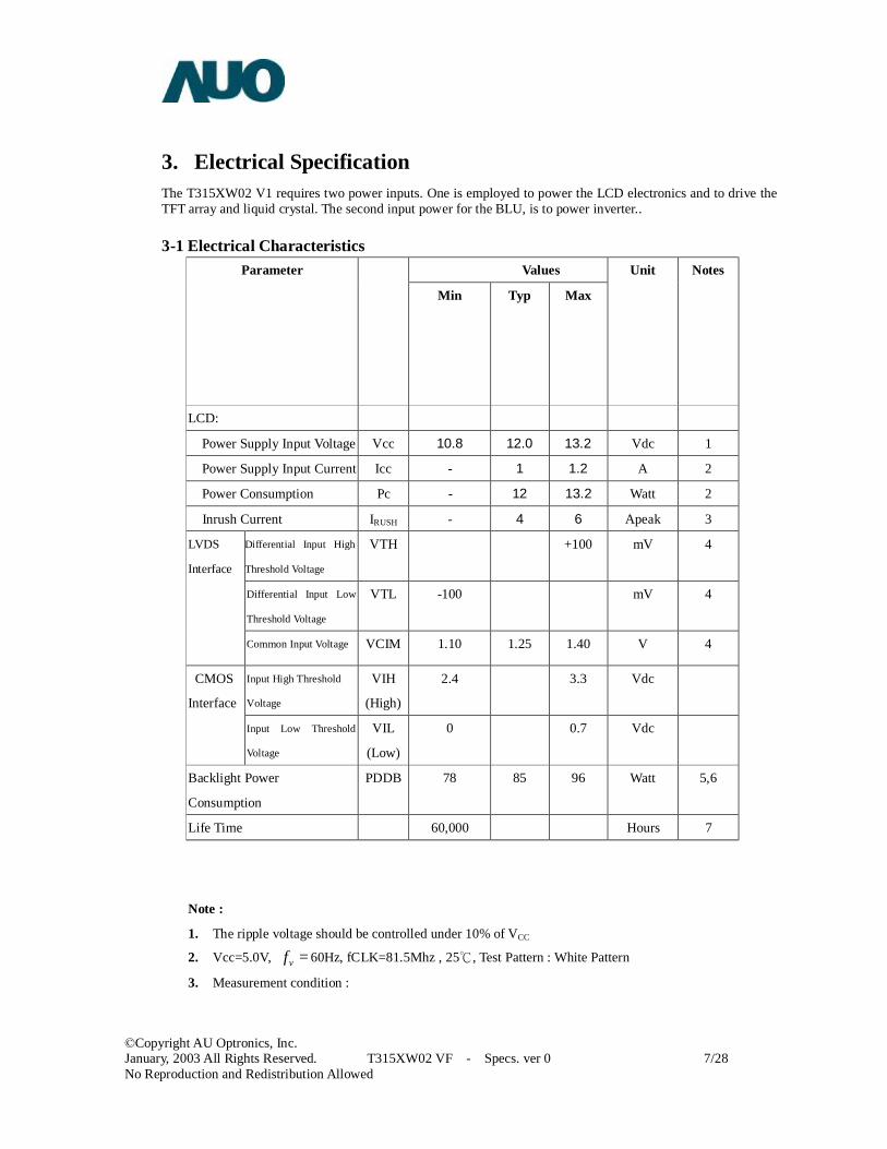
3. Electrical Specification The T315XW02 V1 requires two power inputs. One is employed to power the LCD electronics and to drive the TFT array and liquid crystal. The second input power for the BLU, is to power inverter.. 3-1 Electrical Characteristics
Values Parameter
Min Typ Max
Unit Notes
LCD:
Power Supply Input Voltage Vcc 10.8 12.0 13.2 Vdc 1
Power Supply Input Current Icc - 1 1.2 A 2
Power Consumption Pc - 12 13.2 Watt 2
Inrush Current IRUSH - 4 6 Apeak 3
Differential Input High
Threshold Voltage
VTH +100 mV 4
Differential Input Low
Threshold Voltage
VTL -100 mV 4
LVDS
Interface
Common Input Voltage VCIM 1.10 1.25 1.40 V 4
Input High Threshold
Voltage
VIH
(High)
2.4 3.3 Vdc CMOS
Interface
Input Low Threshold
Voltage
VIL
(Low)
0 0.7 Vdc
Backlight Power
Consumption
PDDB 78 85 96 Watt 5,6
Life Time 60,000 Hours 7
Note :
1. The ripple voltage should be controlled under 10% of VCC
2. Vcc=5.0V, =vf 60Hz, fCLK=81.5Mhz , 25 , Test Pattern : White Pattern℃
3. Measurement condition :
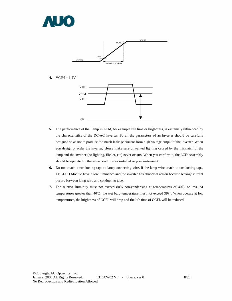
©Copyright AU Optronics, Inc. January, 2003 All Rights Reserved. T315XW02 VF - Specs. ver 0 8/28 No Reproduction and Redistribution Allowed
Trush = 470 uS
10%
90%
VCC
GND
4. VCIM = 1.2V
VTH
VCIM
VTL
0V
5. The performance of the Lamp in LCM, for example life time or brightness, is extremely influenced by
the characteristics of the DC-AC Inverter. So all the parameters of an inverter should be carefully
designed so as not to produce too much leakage current from high-voltage output of the inverter. When
you design or order the inverter, please make sure unwanted lighting caused by the mismatch of the
lamp and the inverter (no lighting, flicker, etc) never occurs. When you confirm it, the LCD Assembly
should be operated in the same condition as installed in your instrument.
6. Do not attach a conducting tape to lamp connecting wire. If the lamp wire attach to conducting tape,
TFT-LCD Module have a low luminance and the inverter has abnormal action because leakage current
occurs between lamp wire and conducting tape.
7. The relative humidity must not exceed 80% non-condensing at temperatures of 40 or less. At ℃
temperatures greater than 40 , the wet bulb temperature must not exceed 39 . When operate at low ℃ ℃
temperatures, the brightness of CCFL will drop and the life time of CCFL will be reduced.
©Copyright AU Optronics, Inc. January, 2003 All Rights Reserved. T315XW02 VF - Specs. ver 0 9/28 No Reproduction and Redistribution Allowed
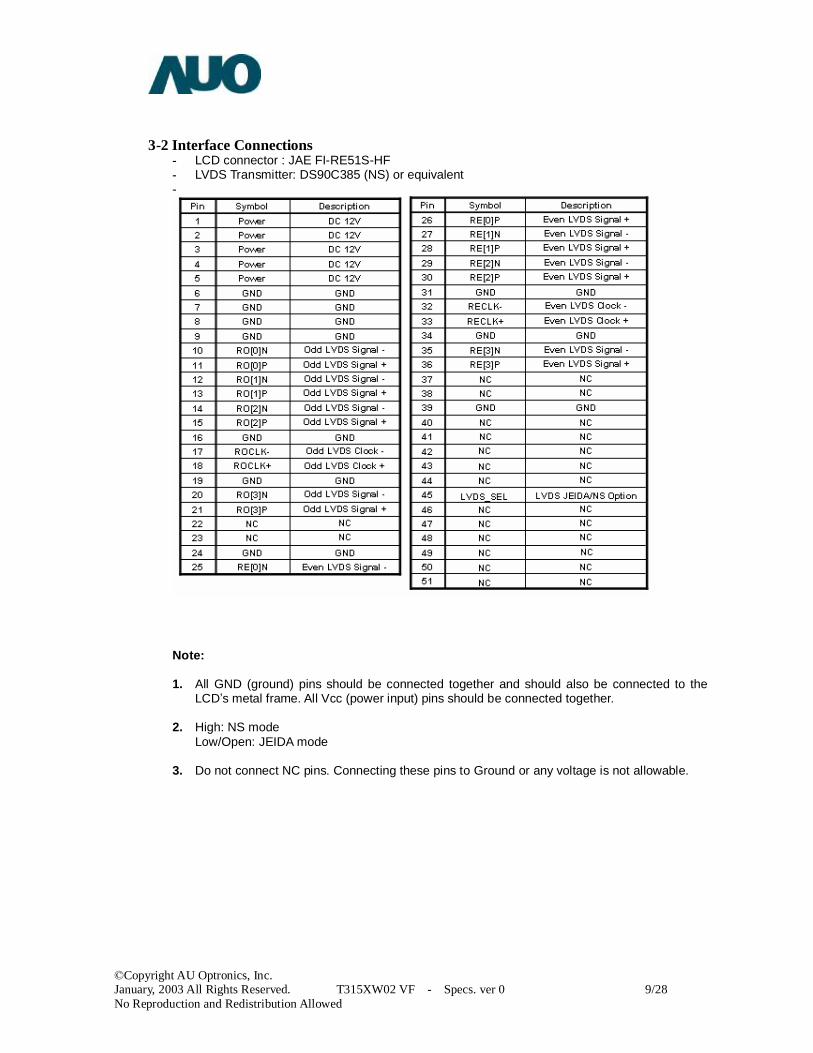
3-2 Interface Connections - LCD connector : JAE FI-RE51S-HF - LVDS Transmitter: DS90C385 (NS) or equivalent -
Note: 1. All GND (ground) pins should be connected together and should also be connected to the
LCD’s metal frame. All Vcc (power input) pins should be connected together. 2. High: NS mode
Low/Open: JEIDA mode
3. Do not connect NC pins. Connecting these pins to Ground or any voltage is not allowable.
©Copyright AU Optronics, Inc. January, 2003 All Rights Reserved. T315XW02 VF - Specs. ver 0 10/28 No Reproduction and Redistribution Allowed
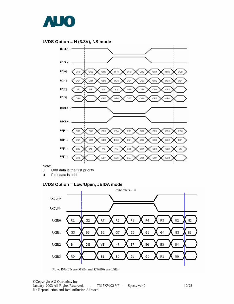
LVDS Option = H (3.3V), NS mode
Note: u Odd data is the first priority. u First data is odd. LVDS Option = Low/Open, JEIDA mode
©Copyright AU Optronics, Inc. January, 2003 All Rights Reserved. T315XW02 VF - Specs. ver 0 11/28 No Reproduction and Redistribution Allowed
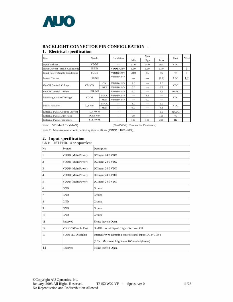
BACKLIGHT CONNECTOR PIN CONFIGURATION - 1. Electrical specification
Min Typ Max
Input Voltage --- 21.6 24.0 26.4 VDCInput Current (Stable Condition) VDDB=24V 3.30 3.50 3.70 1Input Power (Stable Condition) VDDB=24V 78.0 85 96 W 1
Inrush Current VDDB=24V --- --- (6.0) ADC 1,2
ON VDDB=24V 2.0 --- 5.0OFF VDDB=24V 0.0 --- 0.8
On/Off Control Current VDDB=24V 0.0 --- 1.5 mADCMAX VDDB=24V --- 3.3 ---MIN VDDB=24V --- 0.0 ---MAX --- 2.0 --- 5.0MIN --- 0.0 --- 0.8
External PWM Control Current --- --- --- 1.5 mADCExternal PWM Duty Ratio --- 30 --- 100 %External PWM Frequency --- 120 180 300 Hz
Note
D_EPWMF_EPWM
SpecUnitCondition
I_EPWM
IDDB
PWM Function V_PWM VDC
Item Symb.
VDDB
PDDB
IRUSH
IBLON
Dimming Control Voltage VDIM
On/Off Control Voltage VDCVBLON
VDC
Note1 : VDIM= 3.3V (MAX) (Ta=25±5 , Turn on for 45minutes℃ )
Note 2 : Measurement condition Rising time = 20 ms (VDDB : 10%~90%); 2. Input specification CN1: JST PHR-14 or equivalent
No Symbol Description
1 VDDB (Main Power) DC input 24.0 VDC
2 VDDB (Main Power) DC input 24.0 VDC 3 VDDB (Main Power) DC input 24.0 VDC 4 VDDB (Main Power) DC input 24.0 VDC 5 VDDB (Main Power) DC input 24.0 VDC 6 GND Ground
7 GND Ground 8 GND Ground 9 GND Ground 10 GND Ground 11 Reserved Please leave it Open.
12 VBLON (Enable Pin) On/Off control Signal; High: On; Low: Off
13 VDIM (LCD Bright) Internal PWM Dimming control signal input (DC 0~3.3V)
(3.3V : Maximum brightness, 0V min brightness)
14 Reserved Please leave it Open.
©Copyright AU Optronics, Inc. January, 2003 All Rights Reserved. T315XW02 VF - Specs. ver 0 12/28 No Reproduction and Redistribution Allowed
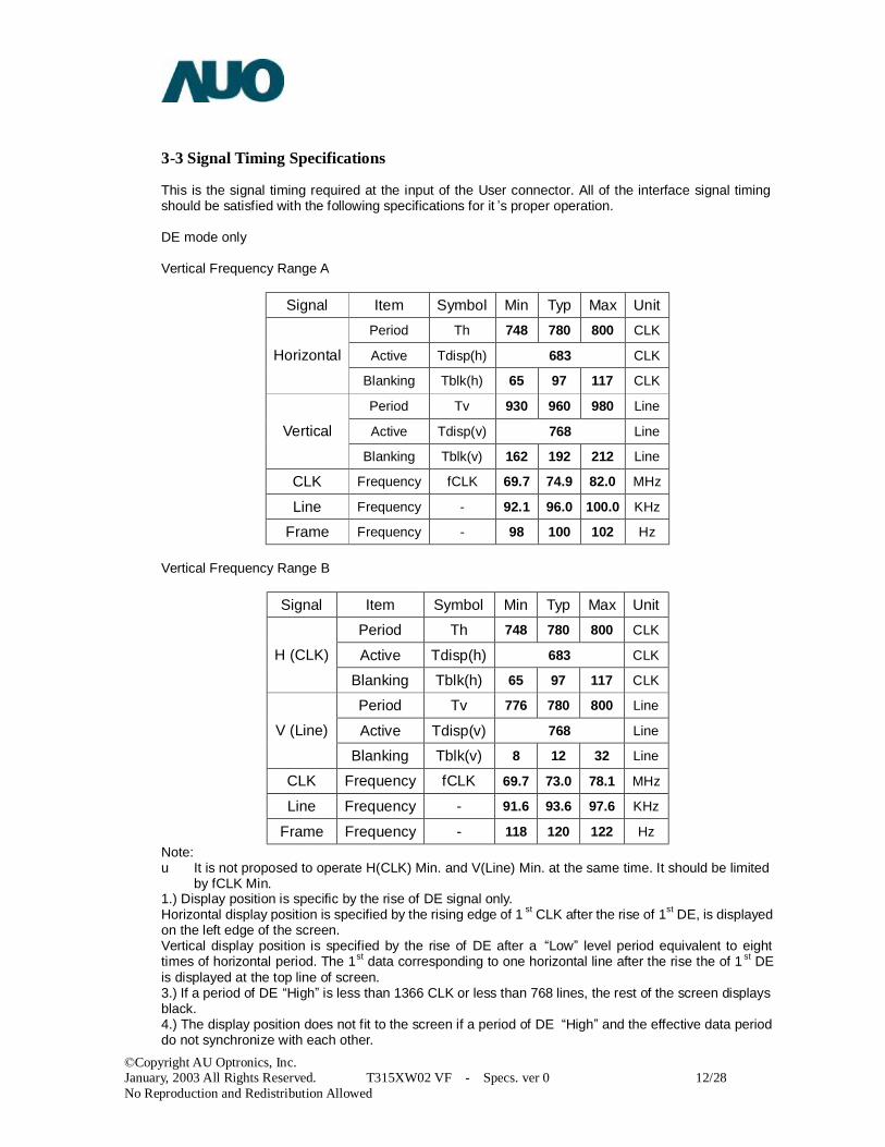
3-3 Signal Timing Specifications This is the signal timing required at the input of the User connector. All of the interface signal timing should be satisfied with the following specifications for it ’s proper operation. DE mode only Vertical Frequency Range A
Signal Item Symbol Min Typ Max Unit Period Th 748 780 800 CLK
Active Tdisp(h) 683 CLK Horizontal
Blanking Tblk(h) 65 97 117 CLK
Period Tv 930 960 980 Line
Active Tdisp(v) 768 Line Vertical
Blanking Tblk(v) 162 192 212 Line
CLK Frequency fCLK 69.7 74.9 82.0 MHz
Line Frequency - 92.1 96.0 100.0 KHz
Frame Frequency - 98 100 102 Hz Vertical Frequency Range B
Signal Item Symbol Min Typ Max Unit
Period Th 748 780 800 CLK
Active Tdisp(h) 683 CLK H (CLK)
Blanking Tblk(h) 65 97 117 CLK
Period Tv 776 780 800 Line
Active Tdisp(v) 768 Line V (Line)
Blanking Tblk(v) 8 12 32 Line
CLK Frequency fCLK 69.7 73.0 78.1 MHz
Line Frequency - 91.6 93.6 97.6 KHz
Frame Frequency - 118 120 122 Hz Note: u It is not proposed to operate H(CLK) Min. and V(Line) Min. at the same time. It should be limited
by fCLK Min. 1.) Display position is specific by the rise of DE signal only. Horizontal display position is specified by the rising edge of 1 st CLK after the rise of 1st DE, is displayed on the left edge of the screen. Vertical display position is specified by the rise of DE after a “Low” level period equivalent to eight times of horizontal period. The 1st data corresponding to one horizontal line after the rise the of 1 st DE is displayed at the top line of screen. 3.) If a period of DE “High” is less than 1366 CLK or less than 768 lines, the rest of the screen displays black. 4.) The display position does not fit to the screen if a period of DE “High” and the effective data period do not synchronize with each other.
©Copyright AU Optronics, Inc. January, 2003 All Rights Reserved. T315XW02 VF - Specs. Ver 0 13/28 No Reproduction and Redistribution Allowed
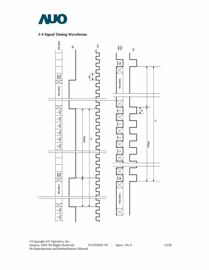
3-4 Signal Timing Waveforms
Th
Tdisp(v)
Tv
DE
RGBData
768Line
Invalid DataInvalid Data
1Line2Line
3Line768Line
4Line
Tclk
CLKDE
RGB DataPixel1366
Invalid DataPixel
1Pixel
2Pixel
3Pixel
4Pixel
5Pixel
6Pixel1366
Invalid DataPixel
1Pixel
2
Th
Tdisp(h)
©Copyright AU Optronics, Inc. January, 2003 All Rights Reserved. T315XW02 VF - Specs. Ver 0 14/28 No Reproduction and Redistribution Allowed
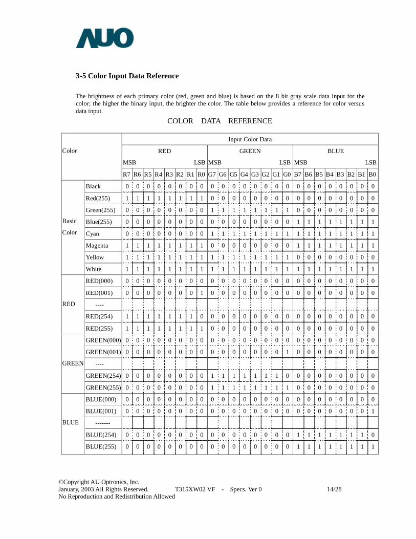
3-5 Color Input Data Reference The brightness of each primary color (red, green and blue) is based on the 8 bit gray scale data input for the color; the higher the binary input, the brighter the color. The table below provides a reference for color versus data input.
COLOR DATA REFERENCE
Input Color Data
RED
MSB LSB
GREEN
MSB LSB
BLUE
MSB LSB
Color
R7 R6 R5 R4 R3 R2 R1 R0 G7 G6 G5 G4 G3 G2 G1 G0 B7 B6 B5 B4 B3 B2 B1 B0
Black 0 0 0 0 0 0 0 0 0 0 0 0 0 0 0 0 0 0 0 0 0 0 0 0
Red(255) 1 1 1 1 1 1 1 1 0 0 0 0 0 0 0 0 0 0 0 0 0 0 0 0
Green(255) 0 0 0 0 0 0 0 0 1 1 1 1 1 1 1 1 0 0 0 0 0 0 0 0
Blue(255) 0 0 0 0 0 0 0 0 0 0 0 0 0 0 0 0 1 1 1 1 1 1 1 1
Cyan 0 0 0 0 0 0 0 0 1 1 1 1 1 1 1 1 1 1 1 1 1 1 1 1
Magenta 1 1 1 1 1 1 1 1 0 0 0 0 0 0 0 0 1 1 1 1 1 1 1 1
Yellow 1 1 1 1 1 1 1 1 1 1 1 1 1 1 1 1 0 0 0 0 0 0 0 0
Basic
Color
White 1 1 1 1 1 1 1 1 1 1 1 1 1 1 1 1 1 1 1 1 1 1 1 1
RED(000) 0 0 0 0 0 0 0 0 0 0 0 0 0 0 0 0 0 0 0 0 0 0 0 0
RED(001) 0 0 0 0 0 0 0 1 0 0 0 0 0 0 0 0 0 0 0 0 0 0 0 0
----
RED(254) 1 1 1 1 1 1 1 0 0 0 0 0 0 0 0 0 0 0 0 0 0 0 0 0
RED
RED(255) 1 1 1 1 1 1 1 1 0 0 0 0 0 0 0 0 0 0 0 0 0 0 0 0
GREEN(000) 0 0 0 0 0 0 0 0 0 0 0 0 0 0 0 0 0 0 0 0 0 0 0 0
GREEN(001) 0 0 0 0 0 0 0 0 0 0 0 0 0 0 0 1 0 0 0 0 0 0 0 0
----
GREEN(254) 0 0 0 0 0 0 0 0 1 1 1 1 1 1 1 0 0 0 0 0 0 0 0 0
GREEN
GREEN(255) 0 0 0 0 0 0 0 0 1 1 1 1 1 1 1 1 0 0 0 0 0 0 0 0
BLUE(000) 0 0 0 0 0 0 0 0 0 0 0 0 0 0 0 0 0 0 0 0 0 0 0 0
BLUE(001) 0 0 0 0 0 0 0 0 0 0 0 0 0 0 0 0 0 0 0 0 0 0 0 1
-------
BLUE(254) 0 0 0 0 0 0 0 0 0 0 0 0 0 0 0 0 1 1 1 1 1 1 1 0
BLUE
BLUE(255) 0 0 0 0 0 0 0 0 0 0 0 0 0 0 0 0 1 1 1 1 1 1 1 1
©Copyright AU Optronics, Inc. January, 2003 All Rights Reserved. T315XW02 VF - Specs. Ver 0 15/28 No Reproduction and Redistribution Allowed
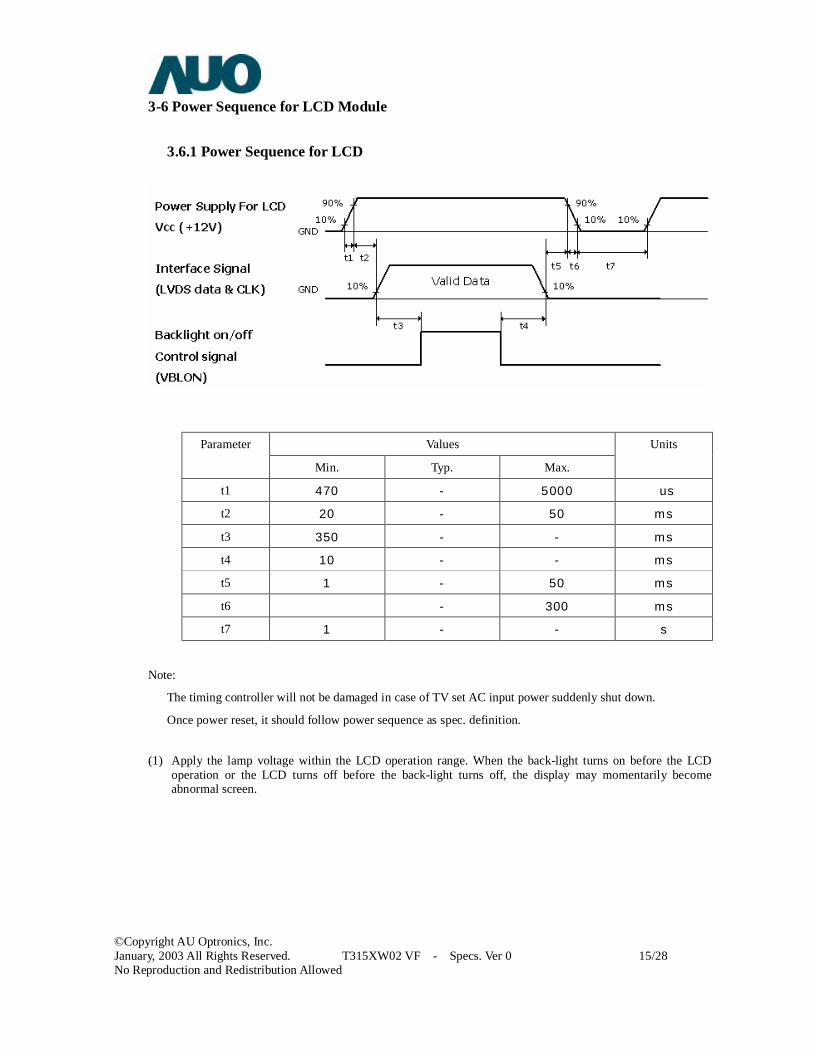
3-6 Power Sequence for LCD Module
3.6.1 Power Sequence for LCD
Values Parameter
Min. Typ. Max.
Units
t1 470 - 5000 us
t2 20 - 50 ms
t3 350 - - ms
t4 10 - - ms
t5 1 - 50 ms
t6 - 300 ms
t7 1 - - s
Note:
The timing controller will not be damaged in case of TV set AC input power suddenly shut down.
Once power reset, it should follow power sequence as spec. definition.
(1) Apply the lamp voltage within the LCD operation range. When the back-light turns on before the LCD
operation or the LCD turns off before the back-light turns off, the display may momentarily become abnormal screen.
©Copyright AU Optronics, Inc. January, 2003 All Rights Reserved. T315XW02 VF - Specs. Ver 0 16/28 No Reproduction and Redistribution Allowed
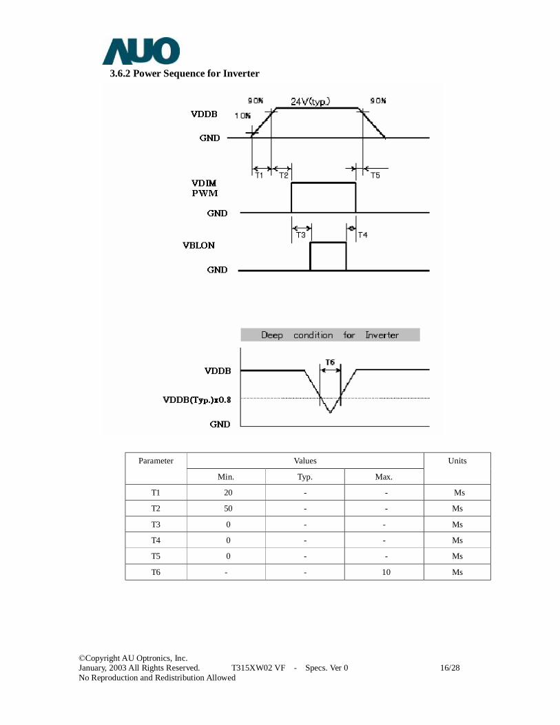
3.6.2 Power Sequence for Inverter
Values Parameter
Min. Typ. Max.
Units
T1 20 - - Ms
T2 50 - - Ms
T3 0 - - Ms
T4 0 - - Ms
T5 0 - - Ms
T6 - - 10 Ms
©Copyright AU Optronics, Inc. January, 2003 All Rights Reserved. T315XW02 VF - Specs. Ver 0 17/28 No Reproduction and Redistribution Allowed
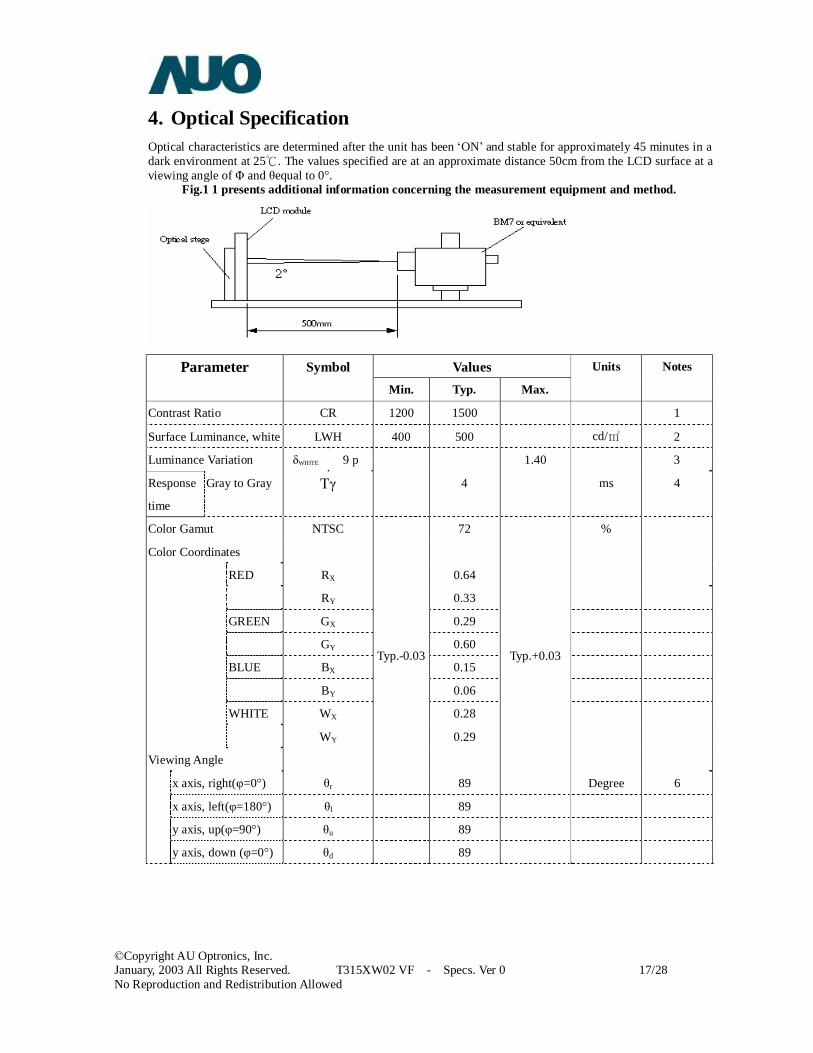
4. Optical Specification Optical characteristics are determined after the unit has been ‘ON’ and stable for approximately 45 minutes in a dark environment at 25 . The values specified are at an approximate distance 50cm from the LCD surface at a ℃viewing angle of Φ and θequal to 0°.
Fig.1 1 presents additional information concerning the measurement equipment and method.
Values Parameter
Symbol Min. Typ. Max.
Units Notes
Contrast Ratio CR 1200 1500 1
Surface Luminance, white LWH 400 500 cd/㎡ 2
Luminance Variation δWHITE 9 p 1.40 3
Response
time
Gray to Gray Tγ 4 ms 4
Color Gamut NTSC 72 %
Color Coordinates
RED RX 0.64
RY 0.33
GREEN GX 0.29
GY 0.60
BLUE BX 0.15
BY 0.06
WHITE WX 0.28
WY
Typ.-0.03
0.29
Typ.+0.03
Viewing Angle
x axis, right(φ=0°) θr 89 Degree 6
x axis, left(φ=180°) θl 89
y axis, up(φ=90°) θu 89
y axis, down (φ=0°) θd 89
©Copyright AU Optronics, Inc. January, 2003 All Rights Reserved. T315XW02 VF - Specs. Ver 0 18/28 No Reproduction and Redistribution Allowed
Note:
1. Contrast Ratio (CR) is defined mathematically as:
Surface Luminance of Lon1 Contrast Ratio=
Surface Luminance of Loff1
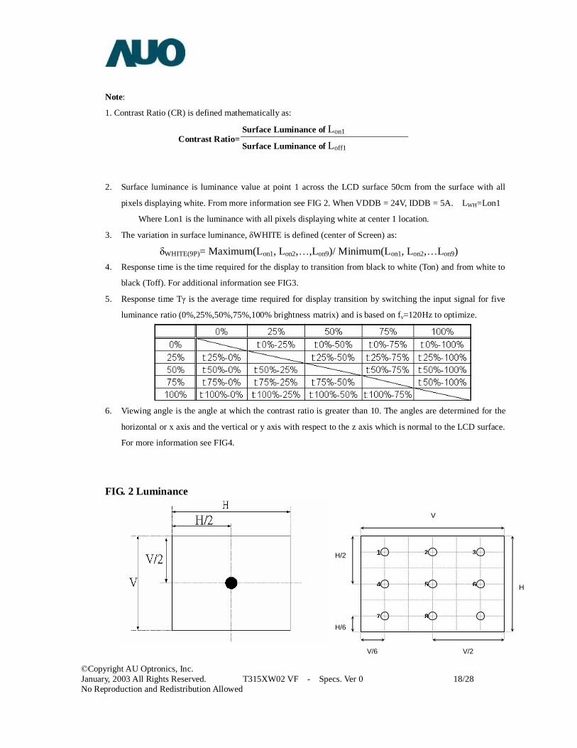
2. Surface luminance is luminance value at point 1 across the LCD surface 50cm from the surface with all
pixels displaying white. From more information see FIG 2. When VDDB = 24V, IDDB = 5A. LWH=Lon1
Where Lon1 is the luminance with all pixels displaying white at center 1 location.
3. The variation in surface luminance, δWHITE is defined (center of Screen) as:
δWHITE(9P)= Maximum(Lon1, Lon2,…,Lon9)/ Minimum(Lon1, Lon2,…Lon9)
4. Response time is the time required for the display to transition from black to white (Ton) and from white to
black (Toff). For additional information see FIG3.
5. Response time Tγ is the average time required for display transition by switching the input signal for five
luminance ratio (0%,25%,50%,75%,100% brightness matrix) and is based on fv=120Hz to optimize.
6. Viewing angle is the angle at which the contrast ratio is greater than 10. The angles are determined for the
horizontal or x axis and the vertical or y axis with respect to the z axis which is normal to the LCD surface.
For more information see FIG4.
FIG. 2 Luminance
1 2 3
4 5 6
7 8
H
V
H/6
H/2
V/2 V/6
©Copyright AU Optronics, Inc. January, 2003 All Rights Reserved. T315XW02 VF - Specs. Ver 0 19/28 No Reproduction and Redistribution Allowed
FIG.3 Response Time The response time is defined as the following figure and shall be measured by switching the input signal for “any level of gray(bright) “ and “any level of gray(dark)”.
Any level of gray(Bright) Any level of gray(Dark) Any level of gray(Bright)
TrR
L0,15,L31,….L255 L0,15,L31,….L255
Photodetector O
utput
Time
L0,15,L31,….L255
FIG.4 Viewing angle
©Copyright AU Optronics, Inc. January, 2003 All Rights Reserved. T315XW02 VF - Specs. Ver 0 20/28 No Reproduction and Redistribution Allowed
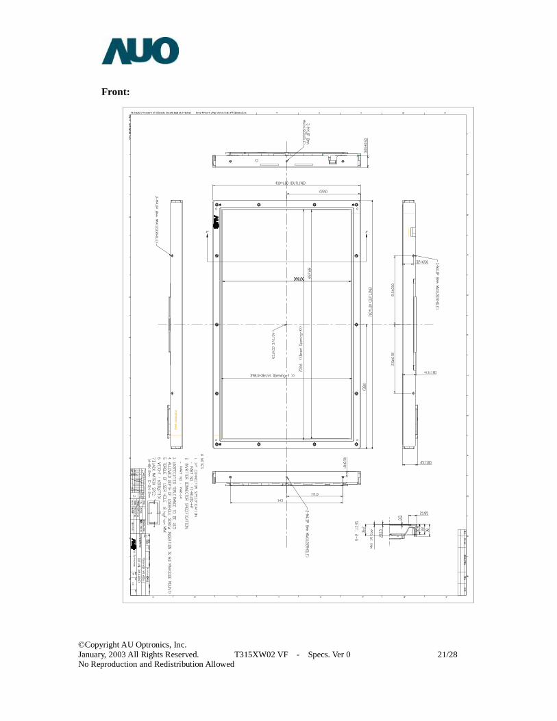
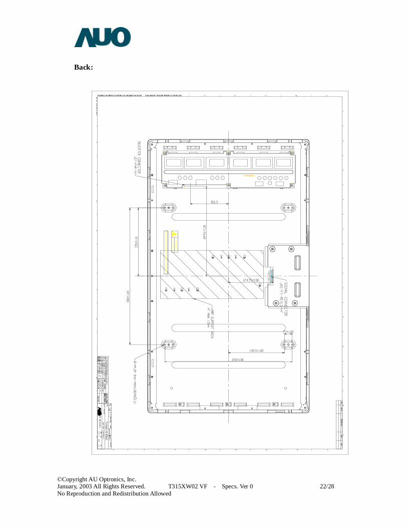
5. Mechanical Characteristics The contents provide general mechanical characteristics for the model T315XW02 V1. In addition the figures in
the next page are detailed mechanical drawing of the LCD.
Horizontal 760.0mm
Vertical 450.0mm
Outline Dimension
Depth 45mm
Horizontal 703.6mm Bezel Opening
Vertical 398.3mm
Horizontal 697.68mm Active Display Area
Vertical 392.26mm
Weight 6500g Typ.
Surface Treatment AG, 3H
©Copyright AU Optronics, Inc. January, 2003 All Rights Reserved. T315XW02 VF - Specs. Ver 0 21/28 No Reproduction and Redistribution Allowed
Front:
©Copyright AU Optronics, Inc. January, 2003 All Rights Reserved. T315XW02 VF - Specs. Ver 0 22/28 No Reproduction and Redistribution Allowed
Back:
PO
WE
R B
EF
OR
E S
ER
VIC
ING
.
HIG
H V
OLT
AG
EC
AU
TIO
ND
ISC
ON
NE
CT T
HE
ELE
CTR
ICR
ISK
OF
ELE
CT
RIC
SH
OC
K.
ME
RC
UR
Y P
LEA
SE
FO
LLO
W L
OC
AL
OR
DIN
AN
CE
S O
R R
EG
ULA
TIO
NS
FO
R D
ISP
OS
AL.
CO
LD
CA
TH
OD
E F
LUO
RE
SC
EN
T L
AM
P IN
LC
D P
AN
EL C
ON
TA
INS
A S
MA
LL A
MO
UN
T O
F
©Copyright AU Optronics, Inc. January, 2003 All Rights Reserved. T315XW02 VF - Specs. Ver 0 23/28 No Reproduction and Redistribution Allowed
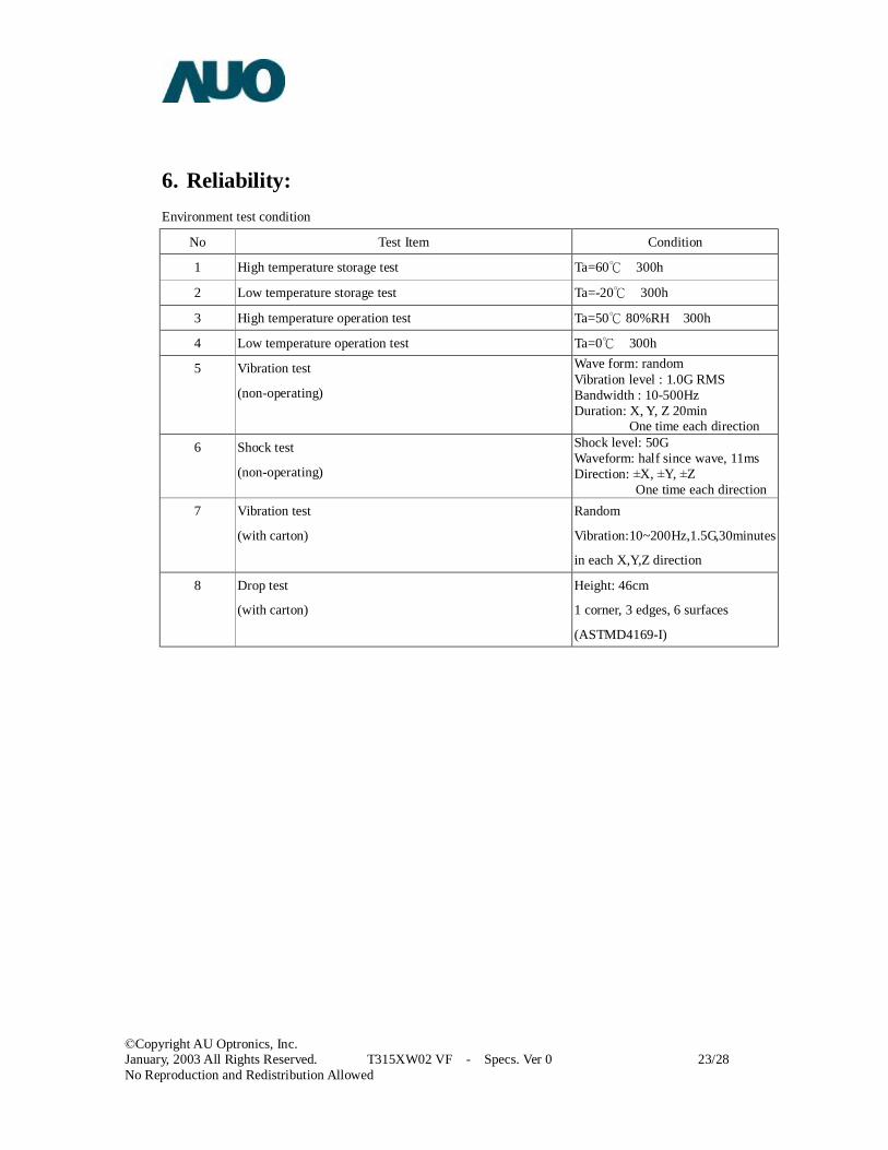
6. Reliability: Environment test condition
No Test Item Condition
1 High temperature storage test Ta=60℃ 300h
2 Low temperature storage test Ta=-20℃ 300h
3 High temperature operation test Ta=50℃ 80%RH 300h
4 Low temperature operation test Ta=0℃ 300h
5 Vibration test
(non-operating)
Wave form: random Vibration level : 1.0G RMS Bandwidth : 10-500Hz Duration: X, Y, Z 20min One time each direction
6 Shock test
(non-operating)
Shock level: 50G Waveform: half since wave, 11ms Direction: ±X, ±Y, ±Z One time each direction
7 Vibration test
(with carton)
Random
Vibration:10~200Hz,1.5G,30minutes
in each X,Y,Z direction
8 Drop test
(with carton)
Height: 46cm
1 corner, 3 edges, 6 surfaces
(ASTMD4169-I)
©Copyright AU Optronics, Inc. January, 2003 All Rights Reserved. T315XW02 VF - Specs. Ver 0 24/28 No Reproduction and Redistribution Allowed
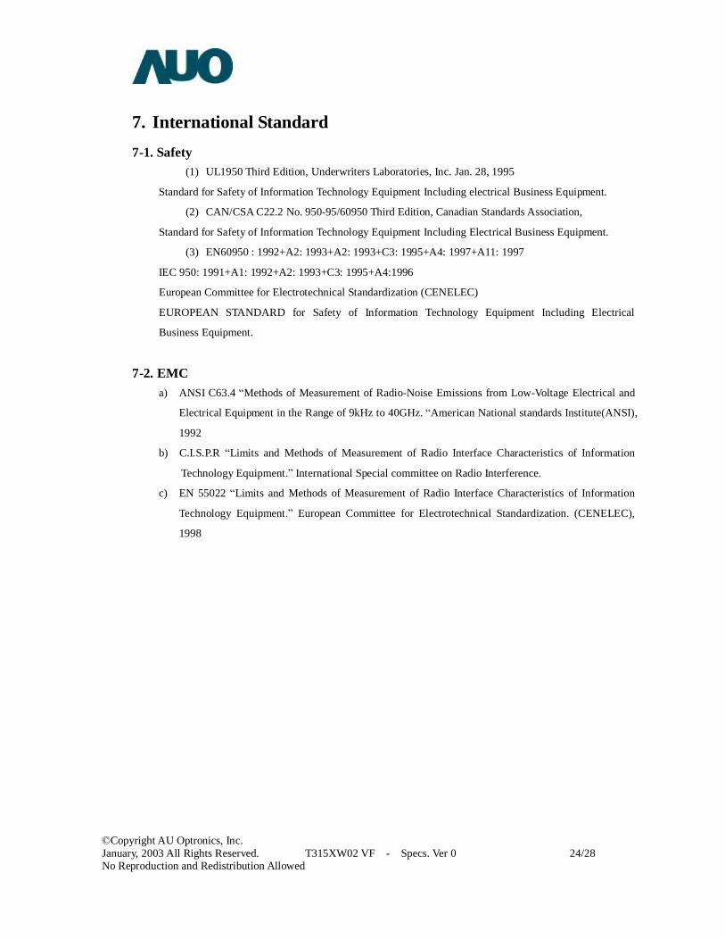
7. International Standard 7-1. Safety
(1) UL1950 Third Edition, Underwriters Laboratories, Inc. Jan. 28, 1995
Standard for Safety of Information Technology Equipment Including electrical Business Equipment.
(2) CAN/CSA C22.2 No. 950-95/60950 Third Edition, Canadian Standards Association,
Standard for Safety of Information Technology Equipment Including Electrical Business Equipment.
(3) EN60950 : 1992+A2: 1993+A2: 1993+C3: 1995+A4: 1997+A11: 1997
IEC 950: 1991+A1: 1992+A2: 1993+C3: 1995+A4:1996
European Committee for Electrotechnical Standardization (CENELEC)
EUROPEAN STANDARD for Safety of Information Technology Equipment Including Electrical
Business Equipment.
7-2. EMC
a) ANSI C63.4 “Methods of Measurement of Radio-Noise Emissions from Low-Voltage Electrical and
Electrical Equipment in the Range of 9kHz to 40GHz. “American National standards Institute(ANSI),
1992
b) C.I.S.P.R “Limits and Methods of Measurement of Radio Interface Characteristics of Information
Technology Equipment.” International Special committee on Radio Interference.
c) EN 55022 “Limits and Methods of Measurement of Radio Interface Characteristics of Information
Technology Equipment.” European Committee for Electrotechnical Standardization. (CENELEC),
1998
©Copyright AU Optronics, Inc. January, 2003 All Rights Reserved. T315XW02 VF - Specs. Ver 0 25/28 No Reproduction and Redistribution Allowed
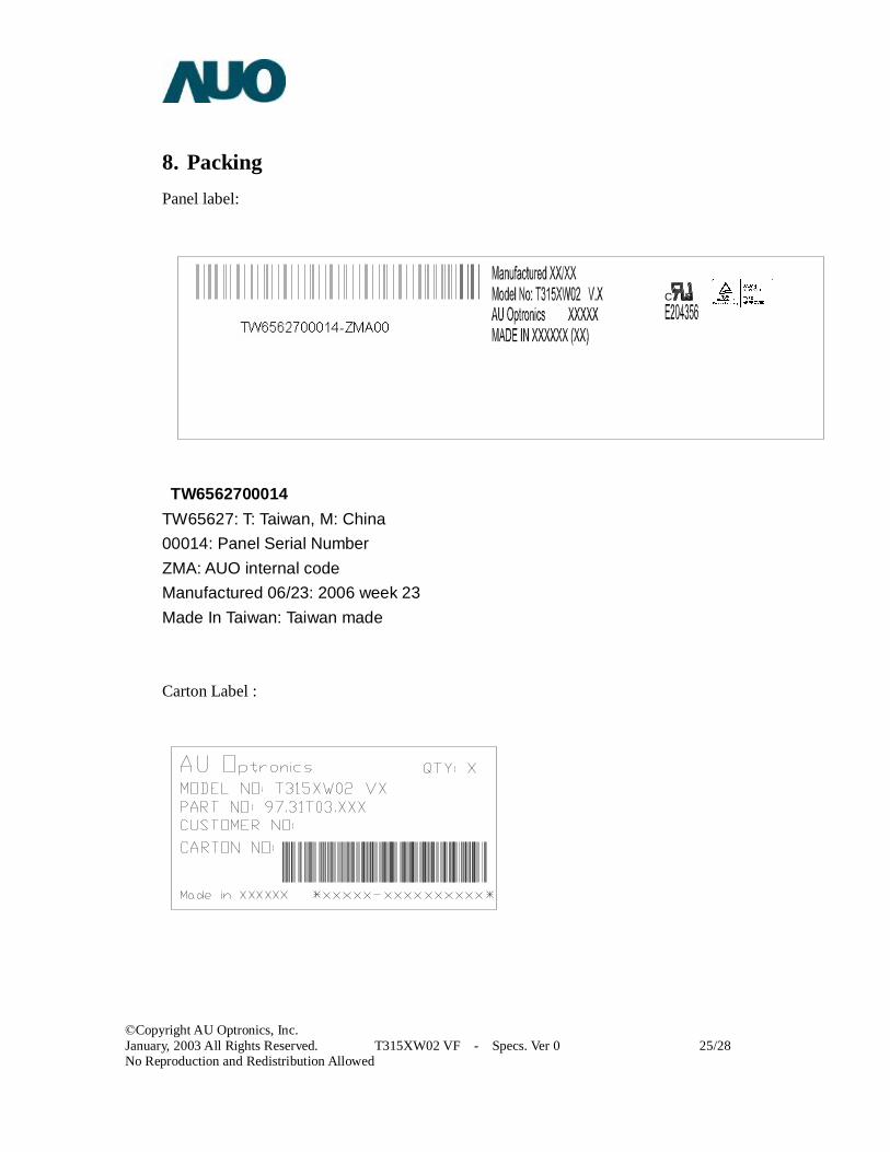
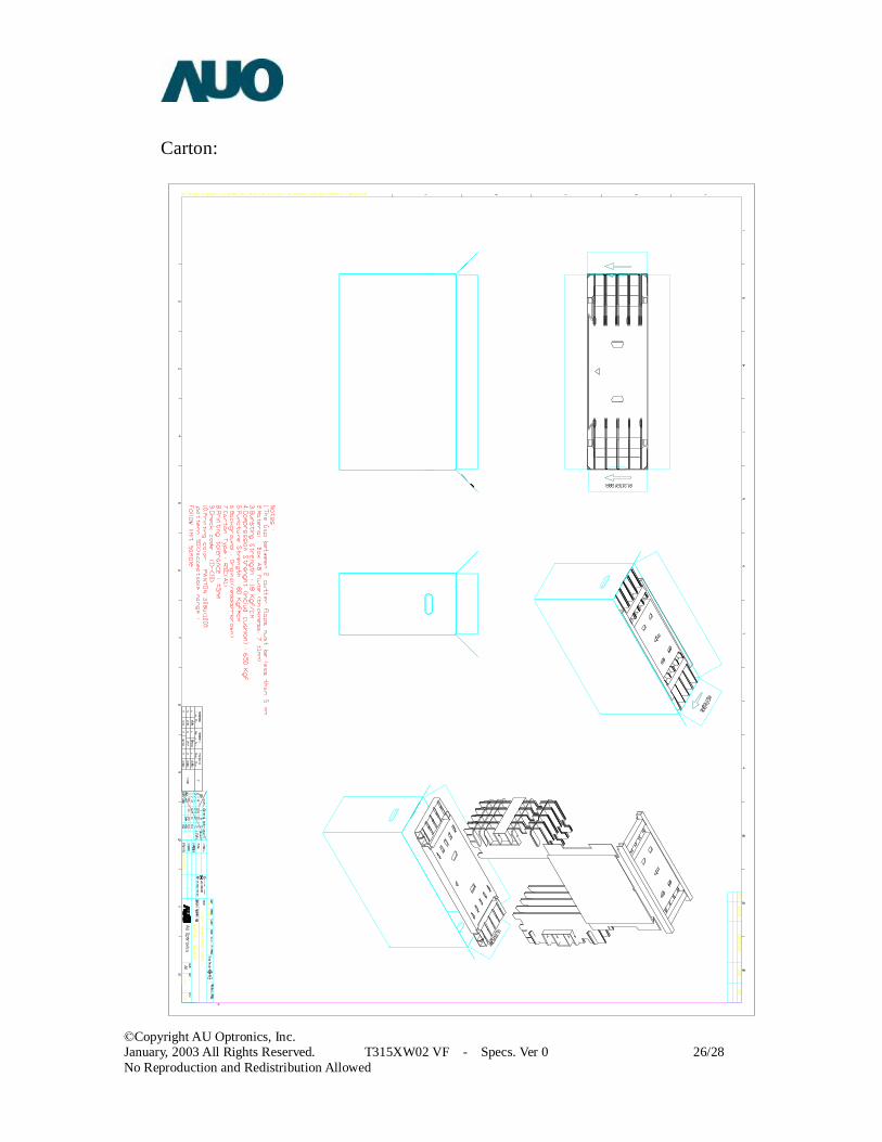
8. Packing Panel label:
C US
TW6562700014 TW65627: T: Taiwan, M: China 00014: Panel Serial Number ZMA: AUO internal code Manufactured 06/23: 2006 week 23 Made In Taiwan: Taiwan made Carton Label :
©Copyright AU Optronics, Inc. January, 2003 All Rights Reserved. T315XW02 VF - Specs. Ver 0 26/28 No Reproduction and Redistribution Allowed
Carton:
©Copyright AU Optronics, Inc. January, 2003 All Rights Reserved. T315XW02 VF - Specs. Ver 0 27/28 No Reproduction and Redistribution Allowed
9. PRECAUTIONS Please pay attention to the followings when you use this TFT LCD module.
9-1 MOUNTING PRECAUTIONS (1) You must mount a module using holes arranged in four corners or four sides. (2) You should consider the mounting structure so that uneven force (ex. Twisted stress) is not applied to module. And the case on which a module is mounted should have sufficient strength so that external force is not transmitted directly to the module. (3) Please attach the surface transparent protective plate to the surface in order to protect the polarizer. Transparent protective plate should have sufficient strength in order to the resist external force. (4) You should adopt radiation structure to satisfy the temperature specification. (5) Acetic acid type and chlorine type materials for the cover case are not desirable because the
former generates corrosive gas of attacking the polarizer at high temperature and the latter causes circuit break by electro-chemical reaction.
(6) Do not touch, push or rub the exposed polarizers with glass, tweezers or anything harder than HB pencil lead. And please do not rub with dust clothes with chemical treatment. Do not touch the surface of polarizer for bare hand or greasy cloth. (Some cosmetics are detrimental to the polarizer.)
(7) When the surface becomes dusty, please wipe gently with absorbent cotton or other soft materials like chamois soaks with petroleum benzene. Normal-hexane is recommended for cleaning the adhesives used to attach front/ rear polarizers. Do not use acetone, toluene and alcohol because they cause chemical damage to the polarizer.
(8) Wipe off saliva or water drops as soon as possible. Their long time contact with polarizer causes deformations and color fading.
(9) Do not open the case because inside circuits do not have sufficient strength.
9-2 OPERATING PRECAUTIONS (1) The spike noise causes the mis-operation of circuits. It should be lower than following voltage:
V=±200mV(Over and under shoot voltage)
(2) Response time depends on the temperature. (In lower temperature, it becomes longer..)
(3) Brightness depends on the temperature. (In lower temperature, it becomes lower.) And in lower
temperature, response time (required time that brightness is stable after turned on) becomes
longer.
(4) Be careful for condensation at sudden temperature change. Condensation makes damage to
polarizer or electrical contacted parts. And after fading condensation, smear or spot will occur.
(5) When fixed patterns are displayed for a long time, remnant image is likely to occur.
(6) Module has high frequency circuits. Sufficient suppression to the electromagnetic interference
shall be done by system manufacturers. Grounding and shielding methods may be important to
minimize the interface.
©Copyright AU Optronics, Inc. January, 2003 All Rights Reserved. T315XW02 VF - Specs. Ver 0 28/28 No Reproduction and Redistribution Allowed
9-3 ELECTROSTATIC DISCHARGE CONTROL Since a module is composed of electronic circuits, it is not strong to electrostatic discharge. Make certain that
treatment persons are connected to ground through wrist band etc. And don’t touch interface pin directly.
9-4 PRECAUTIONS FOR STRONG LIGHT EXPOSURE Strong light exposure causes degradation of polarizer and color filter.
9-5 STORAGE When storing modules as spares for a long time, the following precautions are necessary.
(1) Store them in a dark place. Do not expose the module to sunlight or fluorescent light. Keep the temperature
between 5 and 35 at normal humidity.℃ ℃
(2) The polarizer surface should not come in contact with any other object. It is recommended that they be
stored in the container in which they were shipped.
9-6 HANDLING PRECAUTIONS FOR PROTECTION FILM (1) The protection film is attached to the bezel with a small masking tape. When the protection film is peeled
off, static electricity is generated between the film and polarizer. This should be peeled off slowly and
carefully by people who are electrically grounded and with well ion-blown equipment or in such a
condition, etc.
(2) When the module with protection film attached is stored for a long time, sometimes there remains a very
small amount of flue still on the Bezel after the protection film is peeled off.
(3) You can remove the glue easily. When the glue remains on the Bezel or its vestige is recognized, please
wipe them off with absorbent cotton waste or other soft material like chamois soaked with normal-hexane.