Embed Size (px)
Citation preview
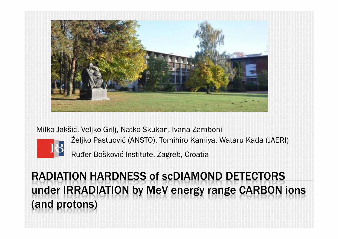
RADIATION HARDNESS of scDIAMOND DETECTORS
under IRRADIATION by MeV energy range CARBON ions
(and protons)
Milko Jakšić, Veljko Grilj, Natko Skukan, Ivana Zamboni
Željko Pastuović (ANSTO), Tomihiro Kamiya, Wataru Kada (JAERI)
Ruđer Bošković Institute, Zagreb, Croatia
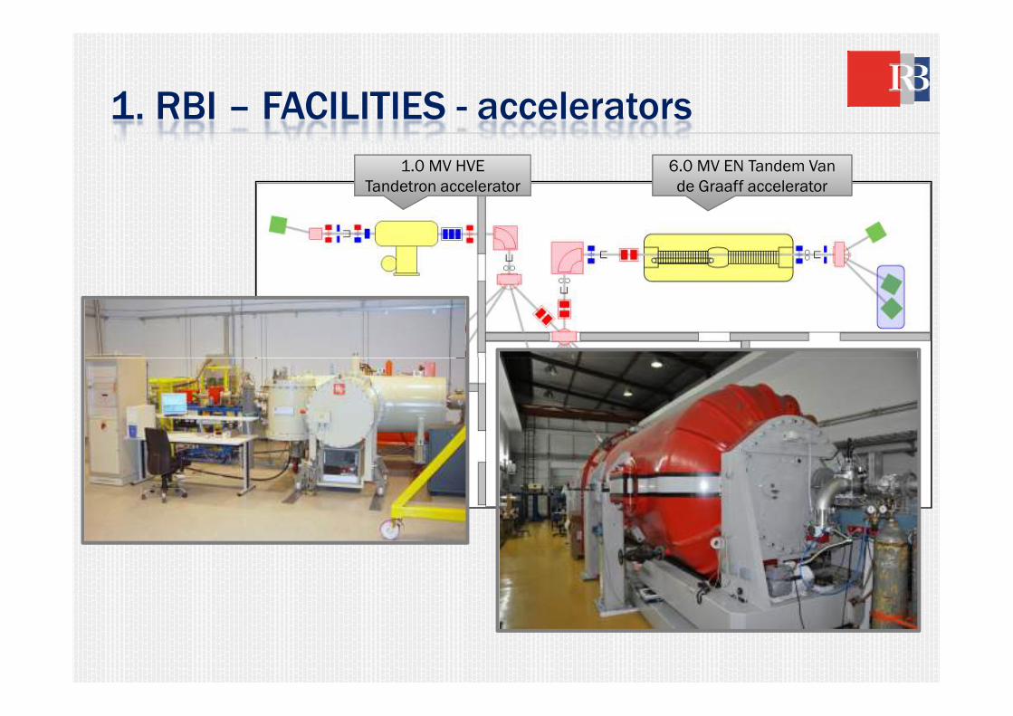
Tandetron accelerator1.0 MV HVE
Tandetron accelerator de Graaff accelerator6.0 MV EN Tandem Van de Graaff accelerator
1. RBI – FACILITIES - accelerators
Tandetron accelerator1.0 MV HVE
Tandetron accelerator de Graaff accelerator6.0 MV EN Tandem Van de Graaff accelerator
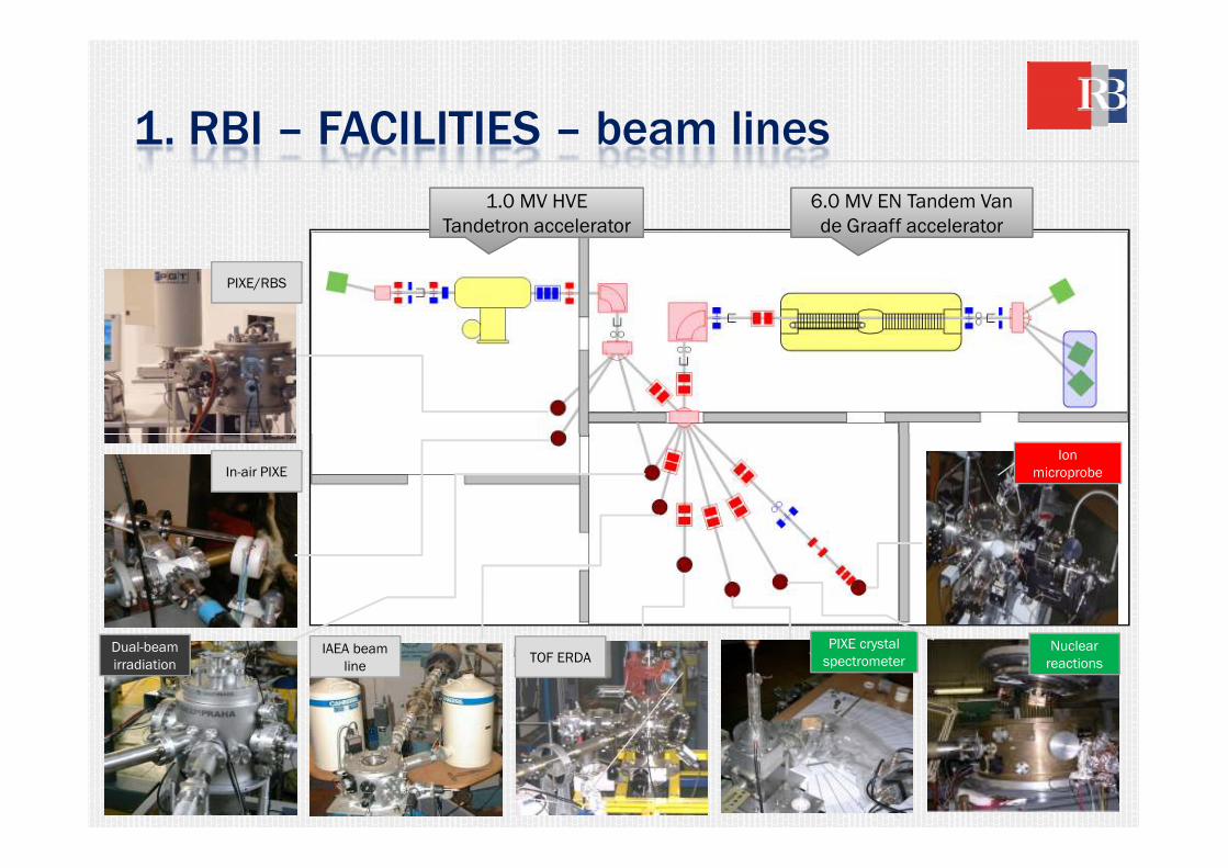
PIXE/RBS
1. RBI – FACILITIES – beam lines
IAEA beam line
TOF ERDADual-beam irradiation
Ion microprobe
Nuclear reactions
In-air PIXE
PIXE crystal spectrometer
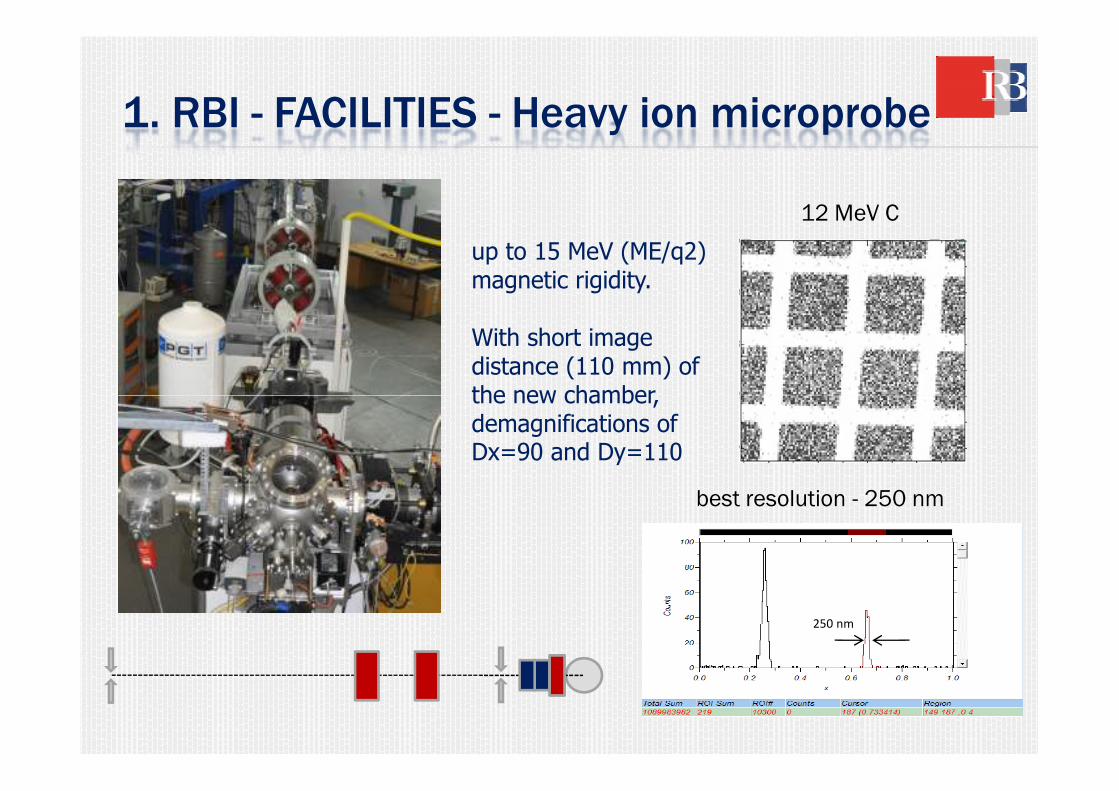
1. RBI - FACILITIES - Heavy ion microprobe
up to 15 MeV (ME/q2) magnetic rigidity.
With short image distance (110 mm) of the new chamber,
12 MeV C
250 nm
the new chamber, demagnifications of Dx=90 and Dy=110
best resolution - 250 nm
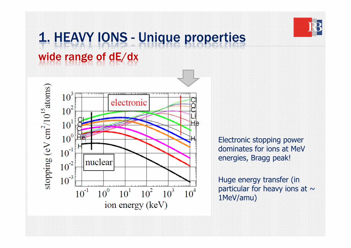
1. HEAVY IONS - Unique properties
wide range of dE/dx
Huge energy transfer (in particular for heavy ions at ~1MeV/amu)
Electronic stopping power dominates for ions at MeV energies, Bragg peak!
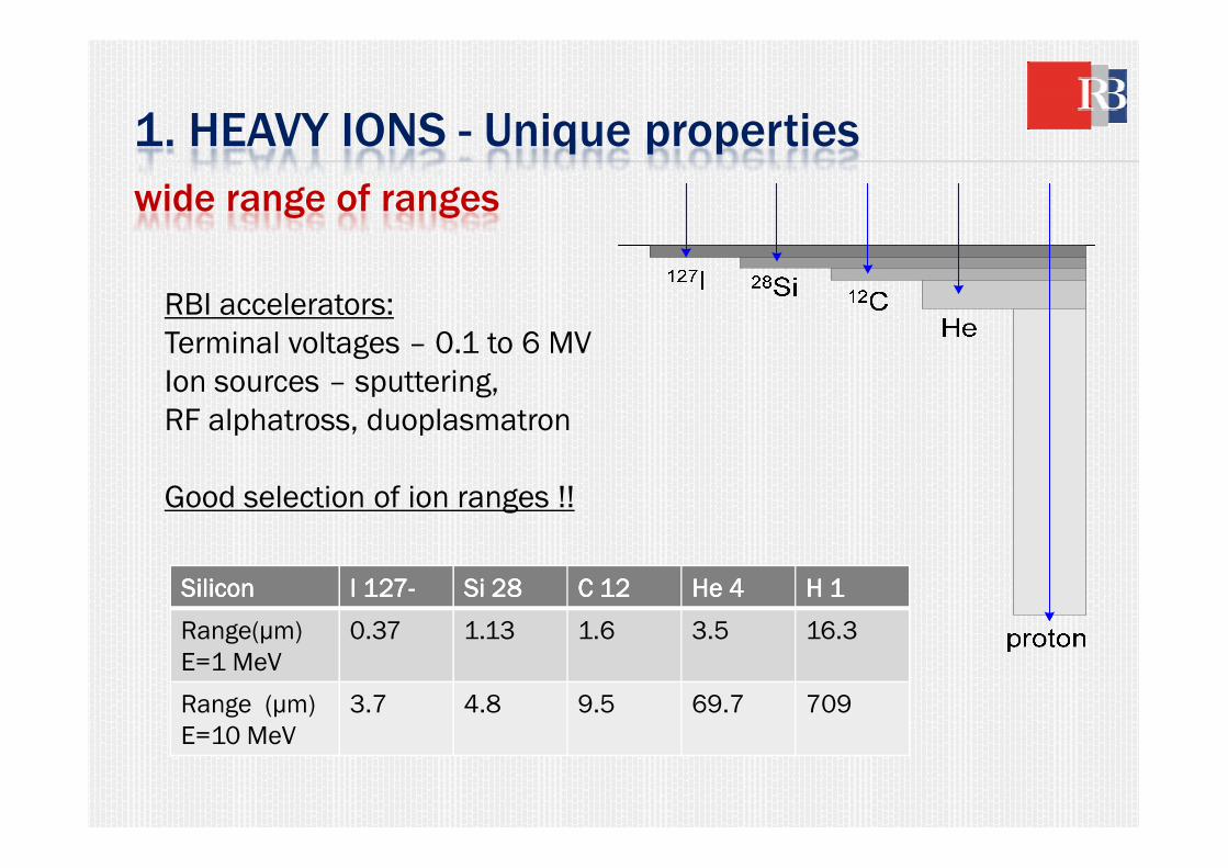
RBI accelerators:Terminal voltages – 0.1 to 6 MVIon sources – sputtering, RF alphatross, duoplasmatron
1. HEAVY IONS - Unique properties
wide range of ranges
SiliconSiliconSiliconSilicon I 127I 127I 127I 127---- Si 28Si 28Si 28Si 28 C 12C 12C 12C 12 He 4He 4He 4He 4 H 1H 1H 1H 1
Range(µm)E=1 MeV
0.37 1.13 1.6 3.5 16.3
Range (µm)E=10 MeV
3.7 4.8 9.5 69.7 709
RF alphatross, duoplasmatron
Good selection of ion ranges !!
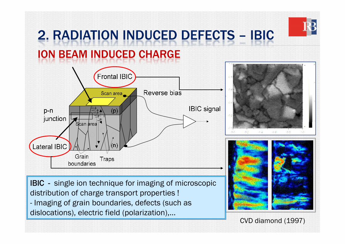
2. RADIATION INDUCED DEFECTS – IBIC
ION BEAM INDUCED CHARGE
IBIC IBIC IBIC IBIC ---- single ion technique for imaging of microscopic distribution of charge transport properties !- Imaging of grain boundaries, defects (such as dislocations), electric field (polarization),...
CVD diamond (1997)
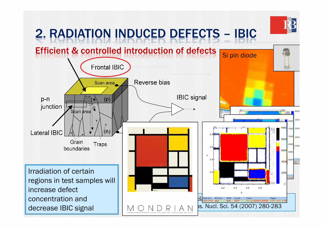
2. RADIATION INDUCED DEFECTS – IBIC
Efficient & controlled introduction of defects Si pin diode
Milko Jakšić et al. IEEE Trans. Nucl. Sci. 54 (2007) 280-283
Irradiation of certain regions in test samples will increase defect concentration and decrease IBIC signal
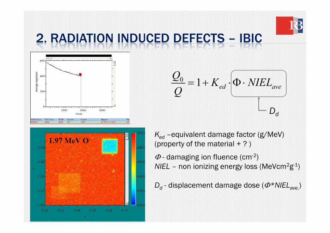
2. RADIATION INDUCED DEFECTS – IBIC
0 1= + ⋅Φ ⋅ed ave
QK NIEL
Q
Dd
1.97 MeV OKed –equivalent damage factor (g/MeV)(property of the material + ? )
Φ - damaging ion fluence (cm-2)NIEL – non ionizing energy loss (MeVcm2g-1)
Dd - displacement damage dose (Φ*NIELave.)
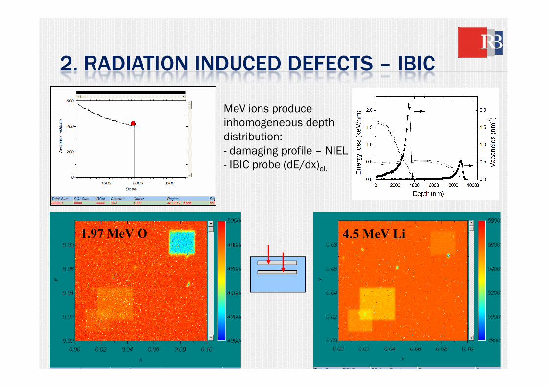
2. RADIATION INDUCED DEFECTS – IBIC
MeV ions produce inhomogeneous depth distribution:- damaging profile – NIEL- IBIC probe (dE/dx)el.
4.5 MeV Li1.97 MeV O
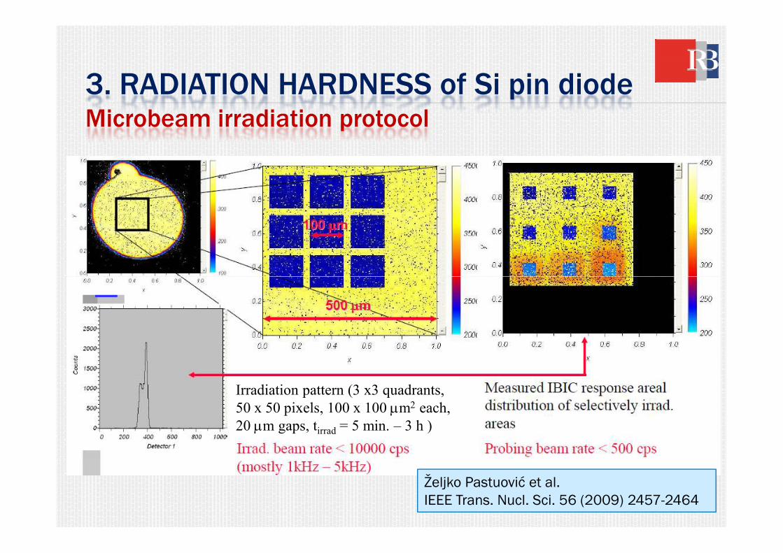
3. RADIATION HARDNESS of Si pin diodeMicrobeam irradiation protocol
Željko Pastuović et al. IEEE Trans. Nucl. Sci. 56 (2009) 2457-2464
Irradiation pattern (3 x3 quadrants,
50 x 50 pixels, 100 x 100 µm2 each,
20 µm gaps, tirrad = 5 min. – 3 h )
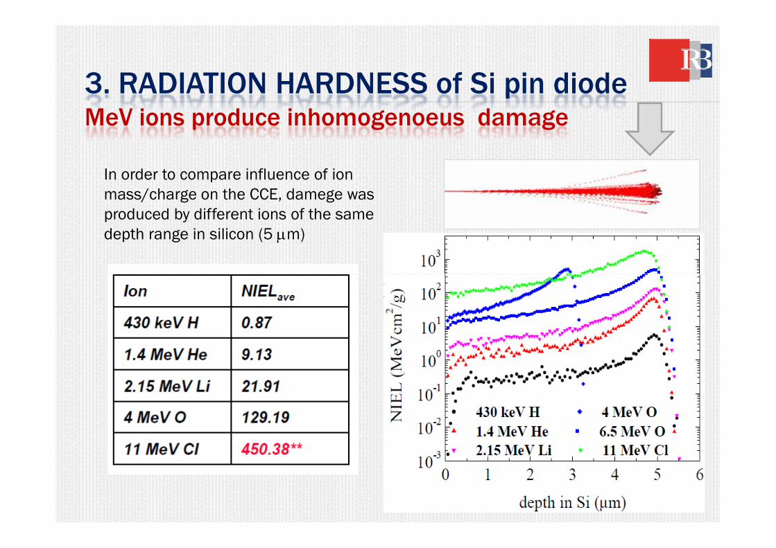
3. RADIATION HARDNESS of Si pin diode MeV ions produce inhomogenoeus damage
In order to compare influence of ion mass/charge on the CCE, damege was produced by different ions of the same depth range in silicon (5 µm)
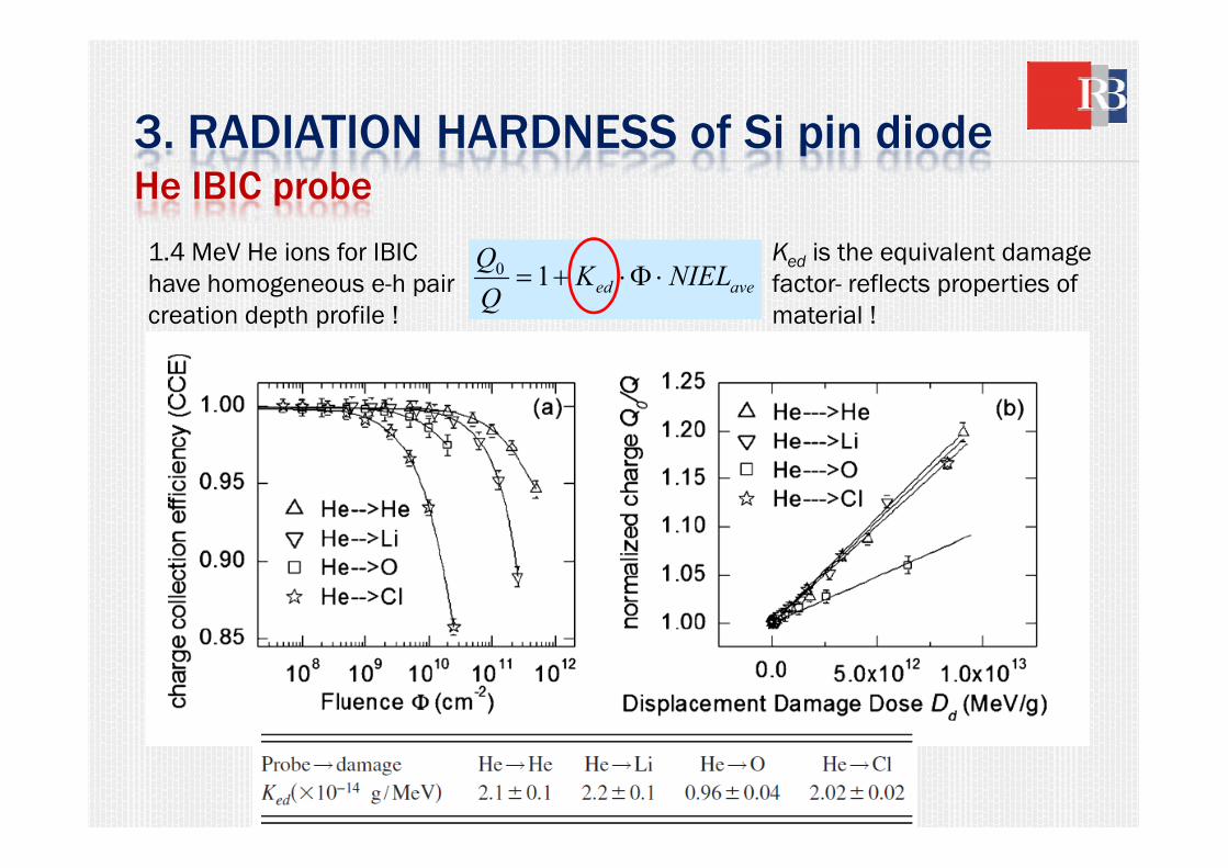
3. RADIATION HARDNESS of Si pin diodeHe IBIC probe
1.4 MeV He ions for IBIC have homogeneous e-h pair creation depth profile !
0 1= + ⋅Φ ⋅ed ave
QK NIEL
Q
Ked is the equivalent damagefactor- reflects properties of material !
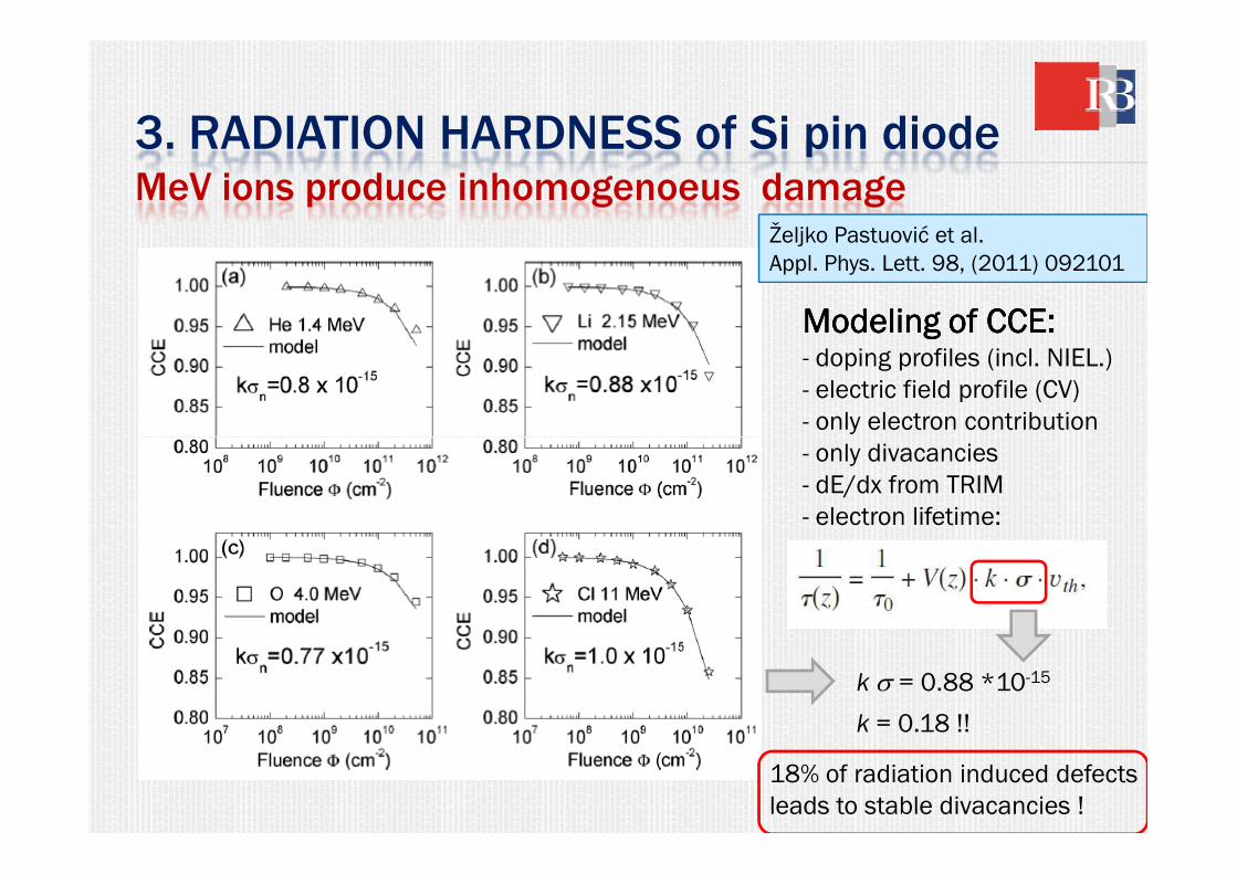
3. RADIATION HARDNESS of Si pin diodeMeV ions produce inhomogenoeus damage
Modeling of CCE:Modeling of CCE:Modeling of CCE:Modeling of CCE:- doping profiles (incl. NIEL.)- electric field profile (CV)- only electron contribution- only divacancies
Željko Pastuović et al. Appl. Phys. Lett. 98, (2011) 092101
- only electron contribution- only divacancies- dE/dx from TRIM- electron lifetime:
k σ = 0.88 *10-15
k = 0.18 !!
18% of radiation induced defects leads to stable divacancies !
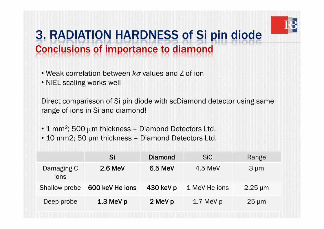
3. RADIATION HARDNESS of Si pin diodeConclusions of importance to diamond
•Weak correlation between kσ values and Z of ion • NIEL scaling works well
Direct comparisson of Si pin diode with scDiamond detector using same range of ions in Si and diamond!range of ions in Si and diamond!
• 1 mm2; 500 µm thickness – Diamond Detectors Ltd.• 10 mm2; 50 µm thickness – Diamond Detectors Ltd.
SiSiSiSi DiamondDiamondDiamondDiamond SiC Range
Damaging C ions
2.6 MeV2.6 MeV2.6 MeV2.6 MeV 6.5 MeV6.5 MeV6.5 MeV6.5 MeV 4.5 MeV 3 µm
Shallow probe 600 keV He ions600 keV He ions600 keV He ions600 keV He ions 430 keV p430 keV p430 keV p430 keV p 1 MeV He ions 2.25 µm
Deep probe 1.3 MeV p1.3 MeV p1.3 MeV p1.3 MeV p 2 MeV p2 MeV p2 MeV p2 MeV p 1.7 MeV p 25 µm
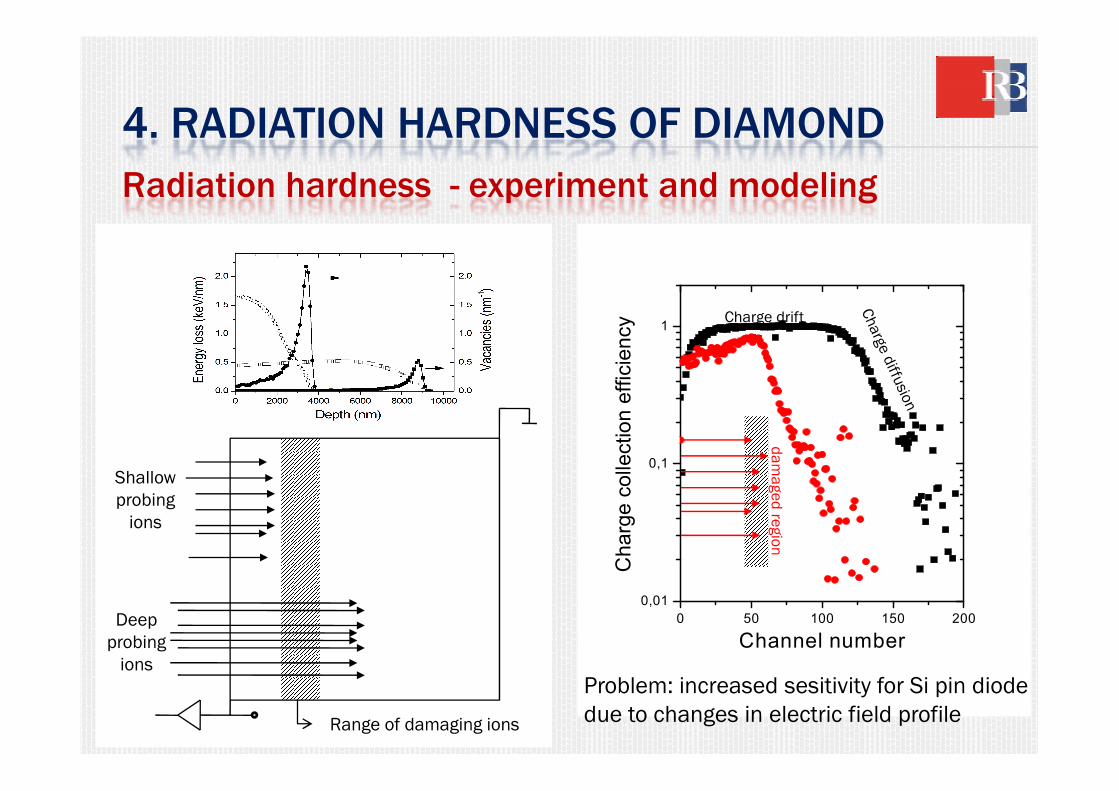
4. RADIATION HARDNESS OF DIAMOND
Radiation hardness - experiment and modeling
1
Charge collection efficiency Charge drift
Shallow probing
ions
Deep probing
ions
Range of damaging ions
0 50 100 150 200
0,01
0,1
Charge collection efficiency
Channel number
da
ma
ged region
Problem: increased sesitivity for Si pin diode due to changes in electric field profile
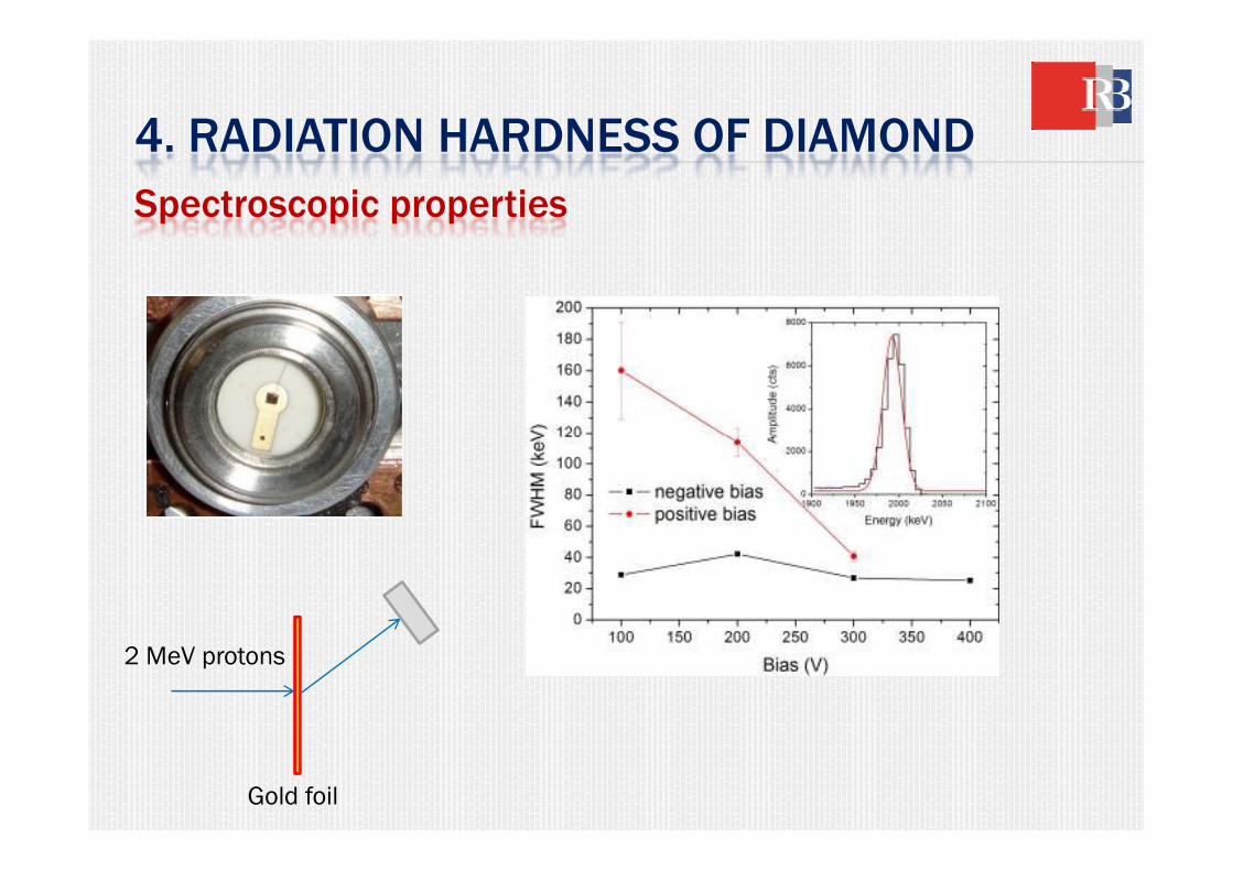
4. RADIATION HARDNESS OF DIAMOND
Spectroscopic properties
2 MeV protons
Gold foil
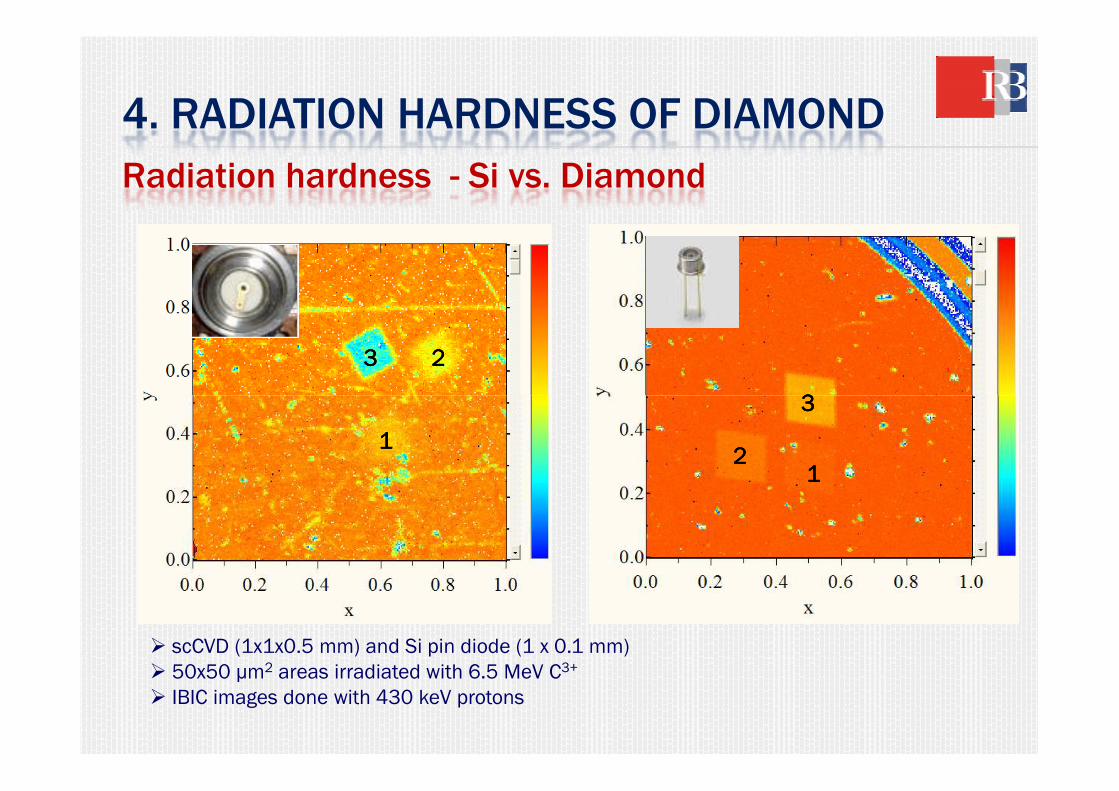
4. RADIATION HARDNESS OF DIAMOND
Radiation hardness - Si vs. Diamond
3333
3333 2222
� scCVD (1x1x0.5 mm) and Si pin diode (1 x 0.1 mm)� 50x50 µm2 areas irradiated with 6.5 MeV C3+
� IBIC images done with 430 keV protons
3333
22221111
1111
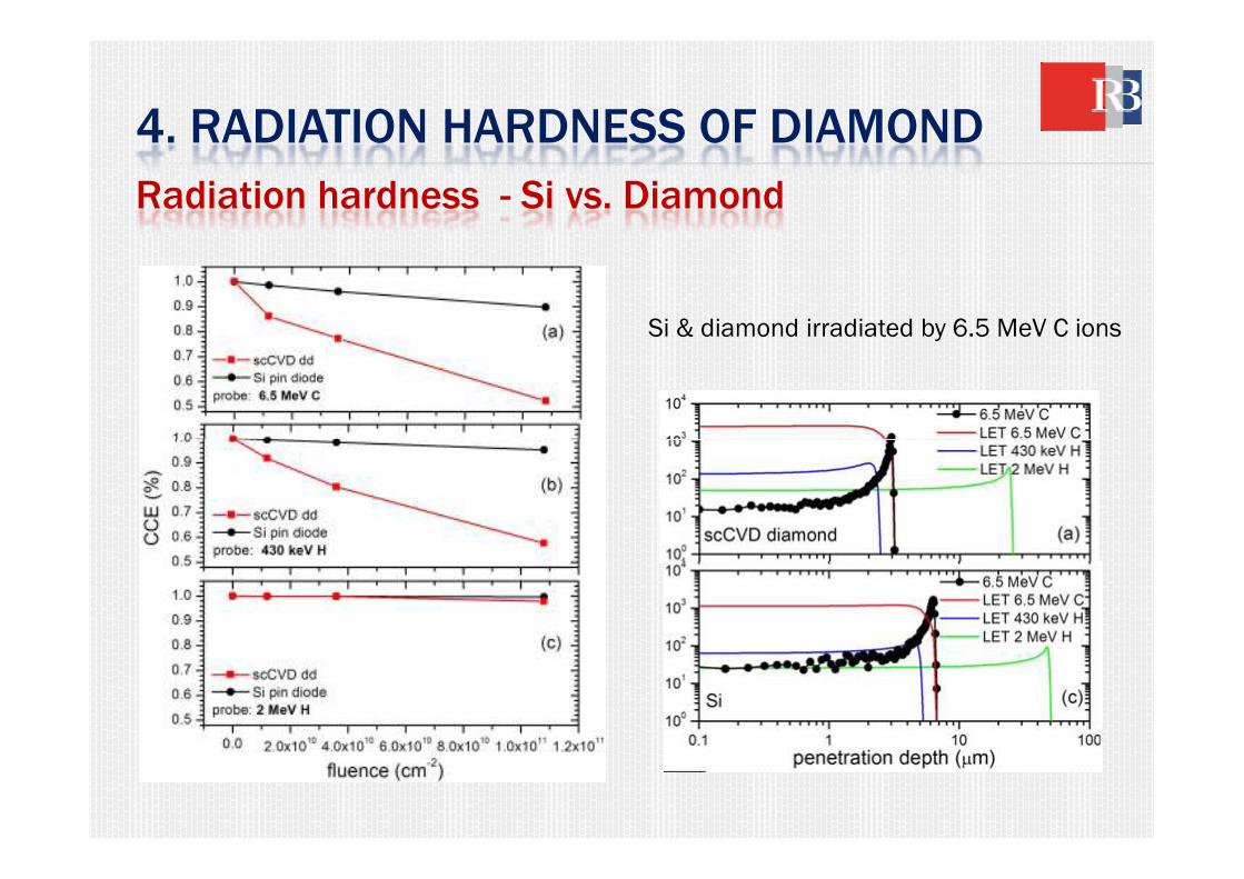
4. RADIATION HARDNESS OF DIAMOND
Radiation hardness - Si vs. Diamond
Si & diamond irradiated by 6.5 MeV C ions
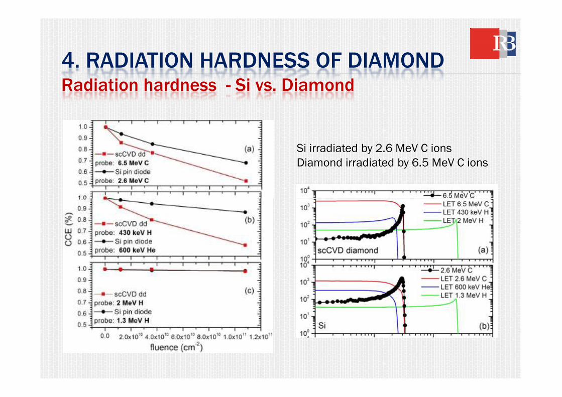
4. RADIATION HARDNESS OF DIAMOND Radiation hardness - Si vs. Diamond
Si irradiated by 2.6 MeV C ionsDiamond irradiated by 6.5 MeV C ions
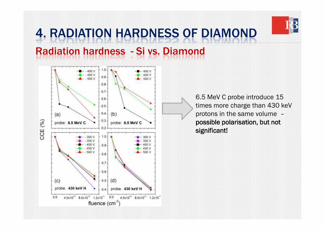
4. RADIATION HARDNESS OF DIAMOND
Radiation hardness - Si vs. Diamond
6.5 MeV C probe introduce 15 times more charge than 430 keV protons in the same volume –protons in the same volume –possible polarisation, but not possible polarisation, but not possible polarisation, but not possible polarisation, but not significant!significant!significant!significant!
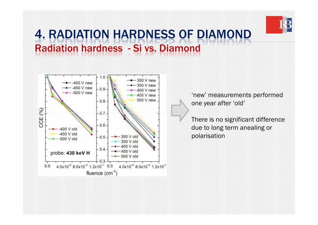
4. RADIATION HARDNESS OF DIAMOND Radiation hardness - Si vs. Diamond
‘new’ measurements performed one year after ‘old’
There is no significant difference due to long term anealing or polarisation
4. RADIATION HARDNESS OF DIAMOND Conclusions
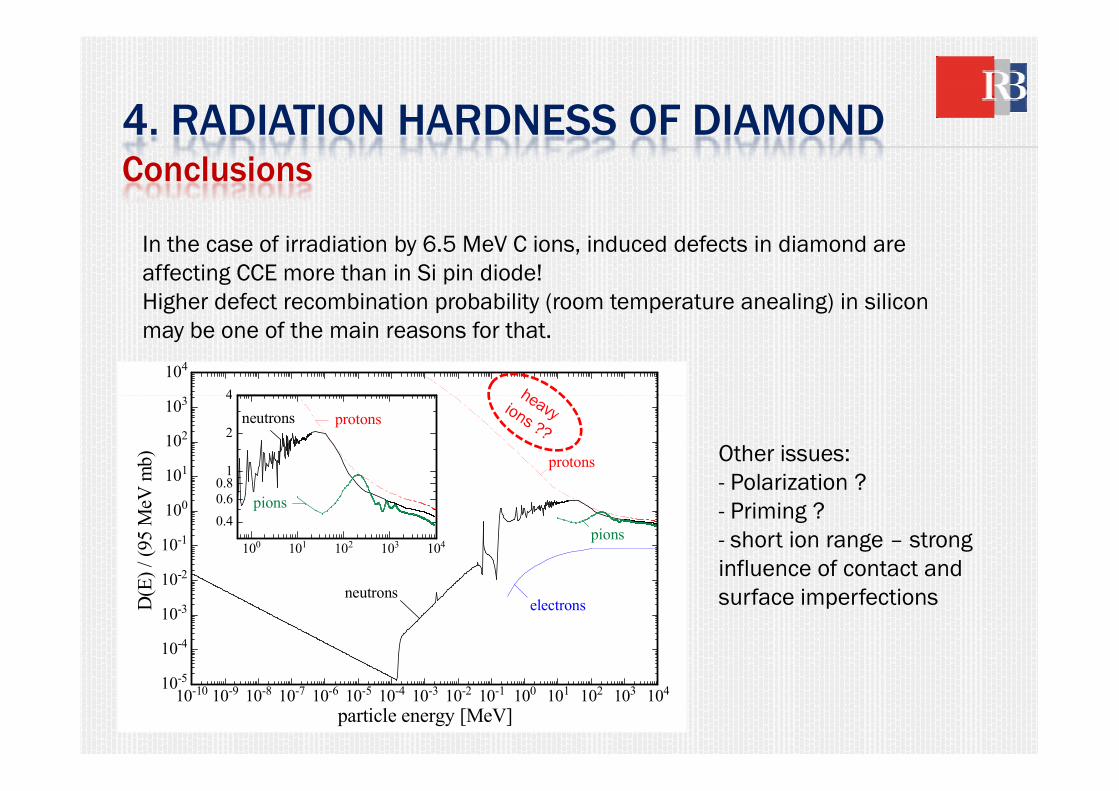
In the case of irradiation by 6.5 MeV C ions, induced defects in diamond are affecting CCE more than in Si pin diode!Higher defect recombination probability (room temperature anealing) in silicon may be one of the main reasons for that.
3
104
4
10-10 10-9 10-8 10-7 10-6 10-5 10-4 10-3 10-2 10-1 100 101 102 103 104
particle energy [MeV]
10-5
10-4
10-3
10-2
10-1
100
101
102
103
D(E) / (95 M
eV mb)
neutronsneutrons
pionspions
protonsprotons
electronselectrons
100 101 102 103 104
0.4
0.6
0.81
2
4
neutronsneutrons
pionspions
protonsprotons
Other issues:- Polarization ?- Priming ?- short ion range – strong influence of contact and surface imperfections
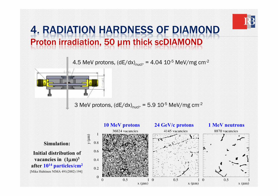
4. RADIATION HARDNESS OF DIAMOND Proton irradiation, 50 µm thick scDIAMOND
4.5 MeV protons, (dE/dx)nucl. = 4.04 10-5 MeV/mg cm-2
Simulation:
Initial distribution of
vacancies in (1µµµµm)3
after 1014 particles/cm2
[Mika Huhtinen NIMA 491(2002) 194]
10 MeV protons 24 GeV/c protons 1 MeV neutrons
3 MeV protons, (dE/dx)nucl. = 5.9 10-5 MeV/mg cm-2
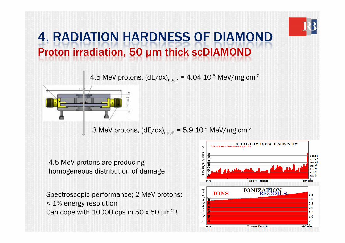
4. RADIATION HARDNESS OF DIAMOND Proton irradiation, 50 µm thick scDIAMOND
4.5 MeV protons, (dE/dx)nucl. = 4.04 10-5 MeV/mg cm-2
3 MeV protons, (dE/dx)nucl. = 5.9 10-5 MeV/mg cm-2
Spectroscopic performance; 2 MeV protons:< 1% energy resolutionCan cope with 10000 cps in 50 x 50 µm2 !
4.5 MeV protons are producing homogeneous distribution of damage
4. RADIATION HARDNESS OF DIAMOND Proton irradiation, 50 µm thick scDIAMOND
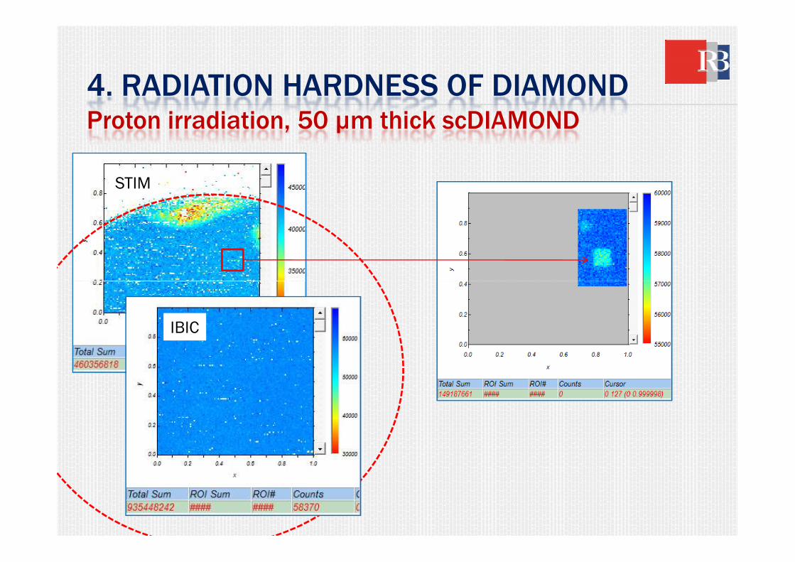
STIM
IBIC
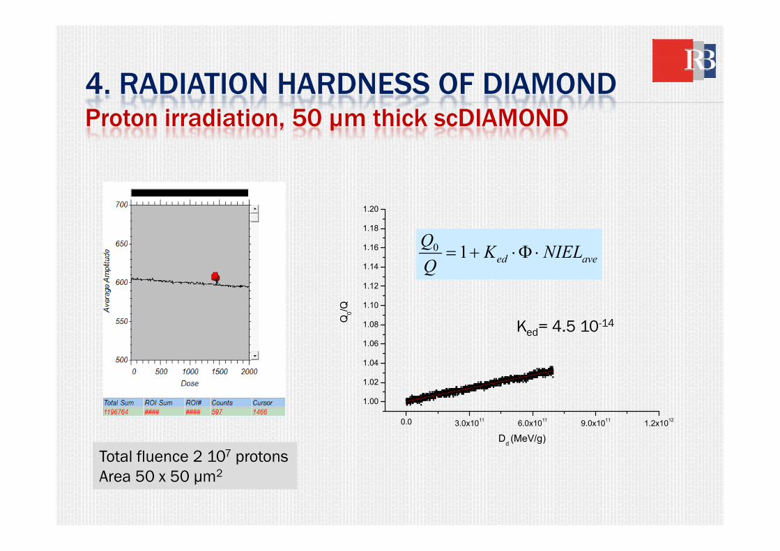
4. RADIATION HARDNESS OF DIAMOND Proton irradiation, 50 µm thick scDIAMOND
1.14
1.16
1.18
1.20
0 1= + ⋅Φ ⋅ed ave
QK NIEL
Q
0.0 3.0x10¹¹
6.0x10¹¹
9.0x10¹¹
1.2x10¹²
1.00
1.02
1.04
1.06
1.08
1.10
1.12
Q0/Q
Dd (MeV/g)
Total fluence 2 107 protonsArea 50 x 50 µm2
Ked= 4.5 10-14
Q
4. RADIATION HARDNESS OF DIAMOND Proton irradiation, 50 µm thick scDIAMOND
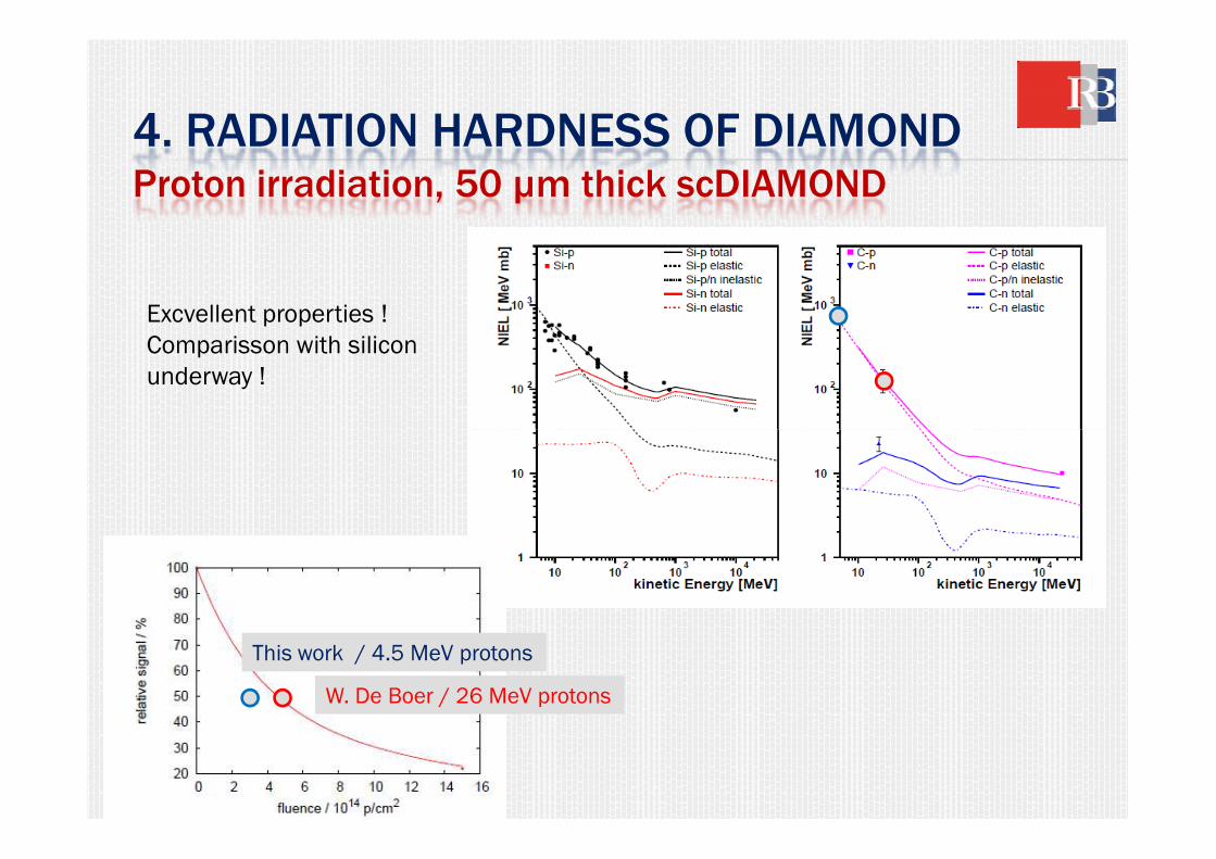
Excvellent properties !Comparisson with silicon underway !
W. De Boer / 26 MeV protons
This work / 4.5 MeV protons
Diamond Detectors -
Development and Applications,
2nd
RBI Detector Workshop, 7-10 May 2012,
Plitvice Lakes National Park, Croatia
Supported by:
• Strategic Japanese-Croatian Cooperative Program on Materials Science
• EU FP7 projects: PARTICLE DETECTORS, SPIRIT, ENSAR • EU FP7 projects: PARTICLE DETECTORS, SPIRIT, ENSAR