Embed Size (px)
Citation preview
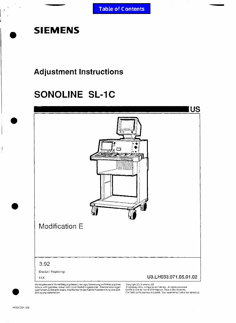
SIEMENS
Adjustment Instructions
SONOLINE SL-1 C
Modification E
3.92 Ersetzt / Replacing:
xxx
~~ ~~-
U3.LH033.071.05.01.02 Wertergabe wie Vswkifaltigung dieser Unterkge. Verwerlung und Mittsilung ihres Ccpyrighf (C) Siemens AG
0
lnhalts nkht geslatw. smveil nitit ausdr0dtlich zugesranden. Zuwiderhandlungen Proprietary data. company mnfidential. All rights resewed. vsrpflichrenzuSchadenersatz.AlieR~htef~rdenFallderPatenferteilungoderGM- Conii6 a lirre de secret d’enrrepwe. Tous drotis r&w&. Einfragung vorbehalten. Confiado corn0 secrelo industrial. Nos reserwnxx tcdos lx derechos.
H033COOl .Uo9
EMEN
Datum/Date Datc/F@da:
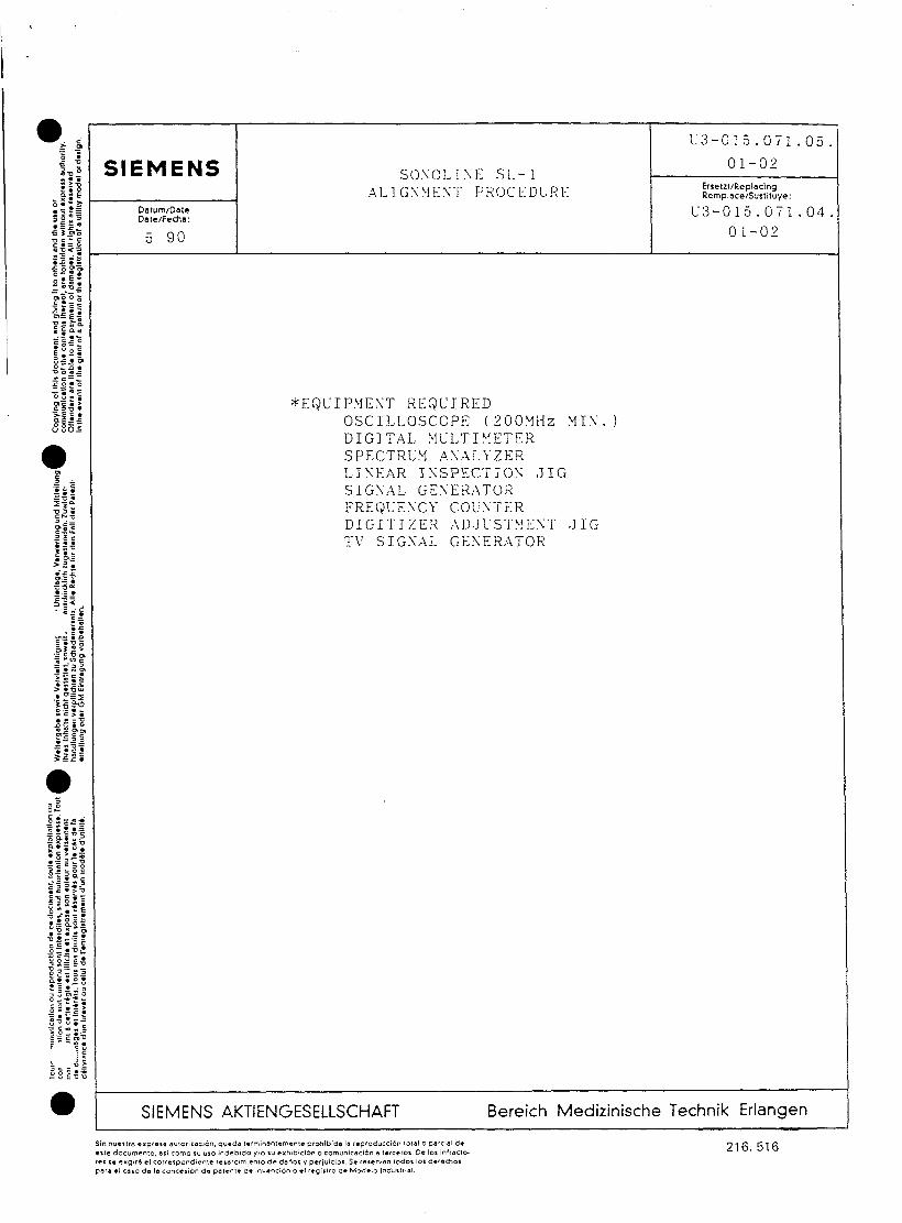
*EQ~IPYEST REQUIRED oscII,LosCoPE ( 2OOYHz YTS. ) DIGTTAL ‘lULTI?lETJ?R SI-‘ECTRL’Y AS;4LI’ZER LISk:AR ISSPECTIOS .JIG SIGXAL GEliER:\TOR FREQUESCY COL‘STER DIGIT? ZER :111.JCST”fk:Z’T .J IG TV SIGSr1L GE-;SERATOR
. 03.
ErretztlReplacing Remplace/Surtituye:
3-015.Oil
SIEMENS AKTIENGESELLSCHAFT Bereich Medizinische Technik Erlangen
ADJUSTMENT PROCEDURES
INDEX
This Adjustment Procedures constituted the following assemblies:
A31 LINEAR-2
A32 ABSTRACTER-4
A33 SECTOR-4
A34 SUPERVISOR-2
A35 DIGITIZER
A36 CONVERTER-2
A37 STORAGER-2
A38 SYNCHRONIZER-2
A40 IMAGER-2
.4PPESDI?l:II.4KDLISG SEQUESCE FOR ADJUSTYENT FOR DIGITAL SECT103
a
G3-01~.071.05 l
I ’ I -
I
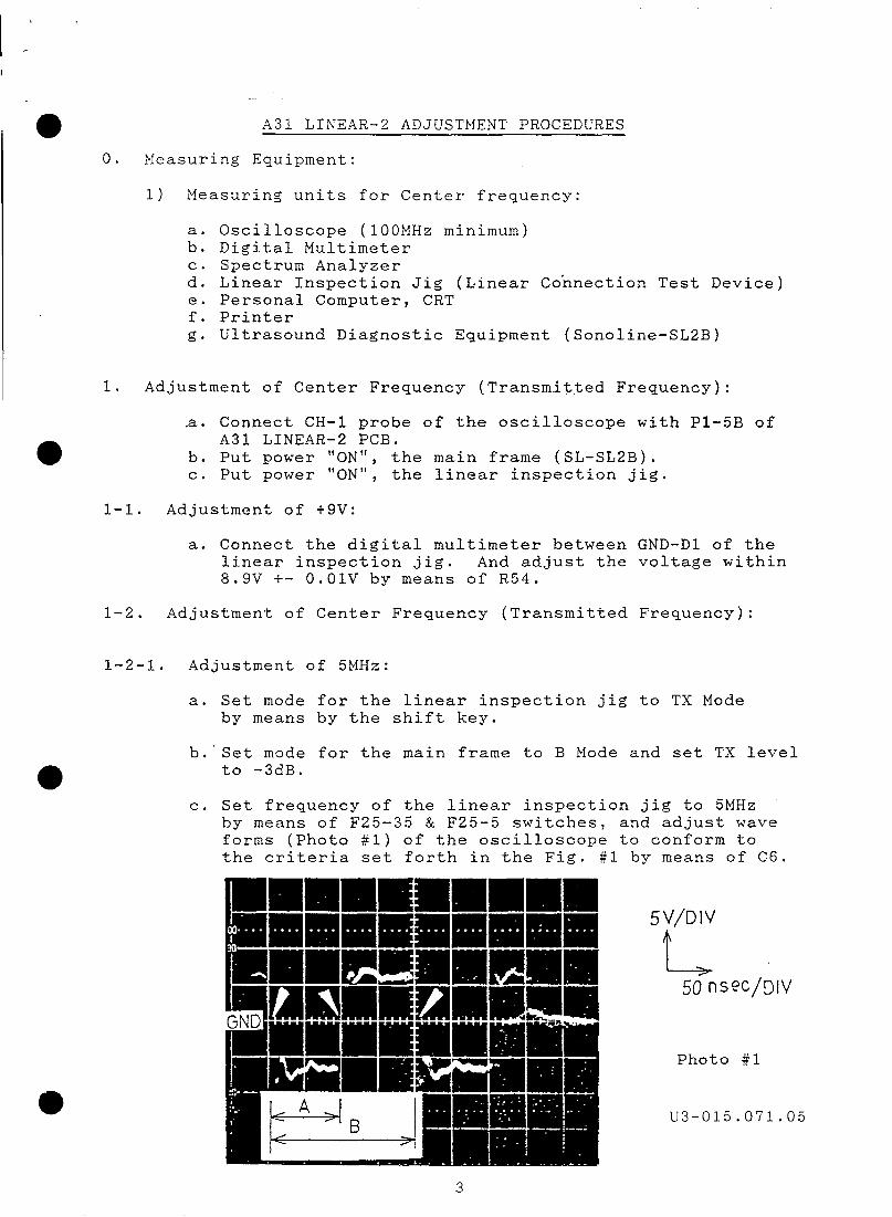
A31 LINEAR-Z ADJUSTMENT PROCEDURES
0. Measuring Equipment:
1) Measuring units for Center frequency:
a. Oscilloscope (100MHz minimum) b. Digital Multimeter c. Spectrum Analyzer d. Linear Inspection Jig (Linear Co'nnection Test Device) e. Personal Computer, CRT f. Printer g* Ultrasound Diagnostic Equipment (Sonoline-SLZB)
1. Adjustment of Center Frequency (Transmitted Frequency):
.a. Connect CH-1 probe of the oscilloscope with Pl-5B of A31 LINEAR-Z PCB.
b. Put power "ON", the main frame (SL-SL2B). c. Put power "ON", the linear inspection jig.
1-l. Adjustment of +9V:
a. Connect the digital multimeter between GND-Dl of the linear inspection jig. And adjust the voltage within 8.9V f- O.OlV by means of R54.
l-2. Adjustment of Center Frequency (Transmitted Frequency):
1-2-1. Adjustment of SMHz:
a. Set mode for the linear inspection jig to TX Mode by means by the shift key.
b.'Set mode for the main frame to B Mode and set TX level to -3dB.
c. Set frequency of the linear inspection jig to 5MHz by means of F25-35 & F25-5 switches, and adjust wave forms (Photo #l) of the oscilloscope to conform to the criteria set forth in the Fig. #1 by means of C6.
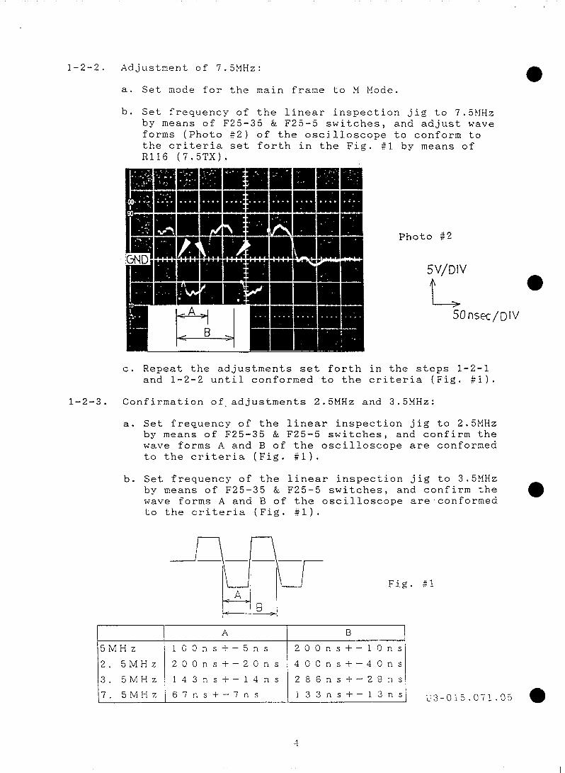
l-2-2. Adjustment of 7.5,LIHz:
a. Set mode for the main frame to M Mode.
b. Set frequency of the linear inspection jig to 7.5HHz by means of F25-35 & F25-5 switches, and adjust wave forms (Photo $2) of the oscilloscope to conform to the criteria set forth in the Fig. $1 by means of R116 (7.5TX).
Photo $2
SV/DlV
L ~~IsPc/DIV
a
c. Repeat the adjustments set forth in the steps l-2-1 and l-2-2 until conformed to the criteria (Fig. fl).
l-2-3. Confirmation of.adjustments 2.5MHz and 3.5MHz:
a. Set frequency of the linear inspection jig to 2.5MHz by means of F25-35 & F25-5 switches, and confirm the wave forms A and B of the oscilloscope are conformed to the criteria (Fig. Xl).
b. Set frequency of the linear inspection jig to 3,5MHz by means of F25-35 & F25-5 switches, and confirm the wave forms A and B of the oscilloscope are.conformed
0
to the criteria (Fig. #l).
Fig. $1
A B
5MHz lOOns+-5ns 200ns+-10ns
2. 5MHz 200ns+-20ns 400ns+-40ns
3. 5MHz 143ns+-14ns 286ns+-29ns
7. 5MHz 67ns+-7ns 133ns+-13ns ~3-015.071.05 a
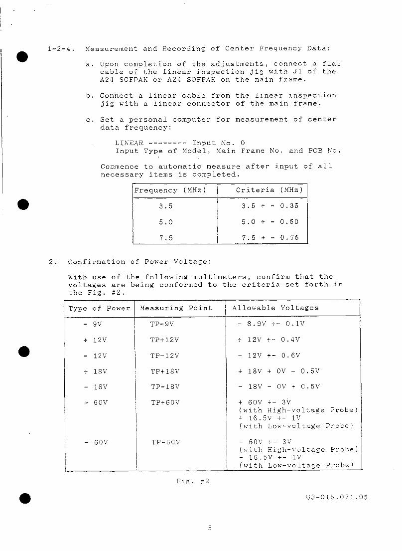
l-2-4. Measurement and Recording of Center Frequency Data:
a. Upon completion of the adjustments, connect a flat cable of the linear inspection jig with Jl of the A24 SOFPAK or A24 SOFPAK on the main frame.
b. Connect a linear cable from the linear inspection jig with a linear connector of the main frame.
c. Set a personal computer for measurement of center data frequency:
LINEAR -------- Input No. 0 Input Type of Model, Main Frame No. and PCB No.
Commence to automatic measure after input of all necessary items is completed.
Frequency (MHz) Criteria (MHz)
3.5 3.5 + - 0.35
5.0 5.0 i - 0.50
7.5 7.5 + - 0.75
2. Confirmation of Power Voltage:
With use of the following multimeters, confirm that the voltages are being conformed to the criteria set forth in the Fig. +2.
Type of Power ?feasuring Point Allowable Voltages
- 9v TP-9V - 0.9v +- O.lV
-t 12v TPtl2V -I- 12V t- 0.4v
- 12v TP-12V - 12V +- 0.6V
i 18V TP+18V f 18V -t OV - 0.5V
- 18V TP-18V - 18V - ov t 0.5v
i- 6OV TPtGOV + 6OV t- 3V (with High-voltage Probe) t 16.sV t- IV (with Low-voltage Probe)
- 6OV TP-GOV - 6OV t- 3V (with High-voltage Probe) - 16.5V t- 1V (with Low-voltage Probe)
Fig. +2
b3-015.071.05
5
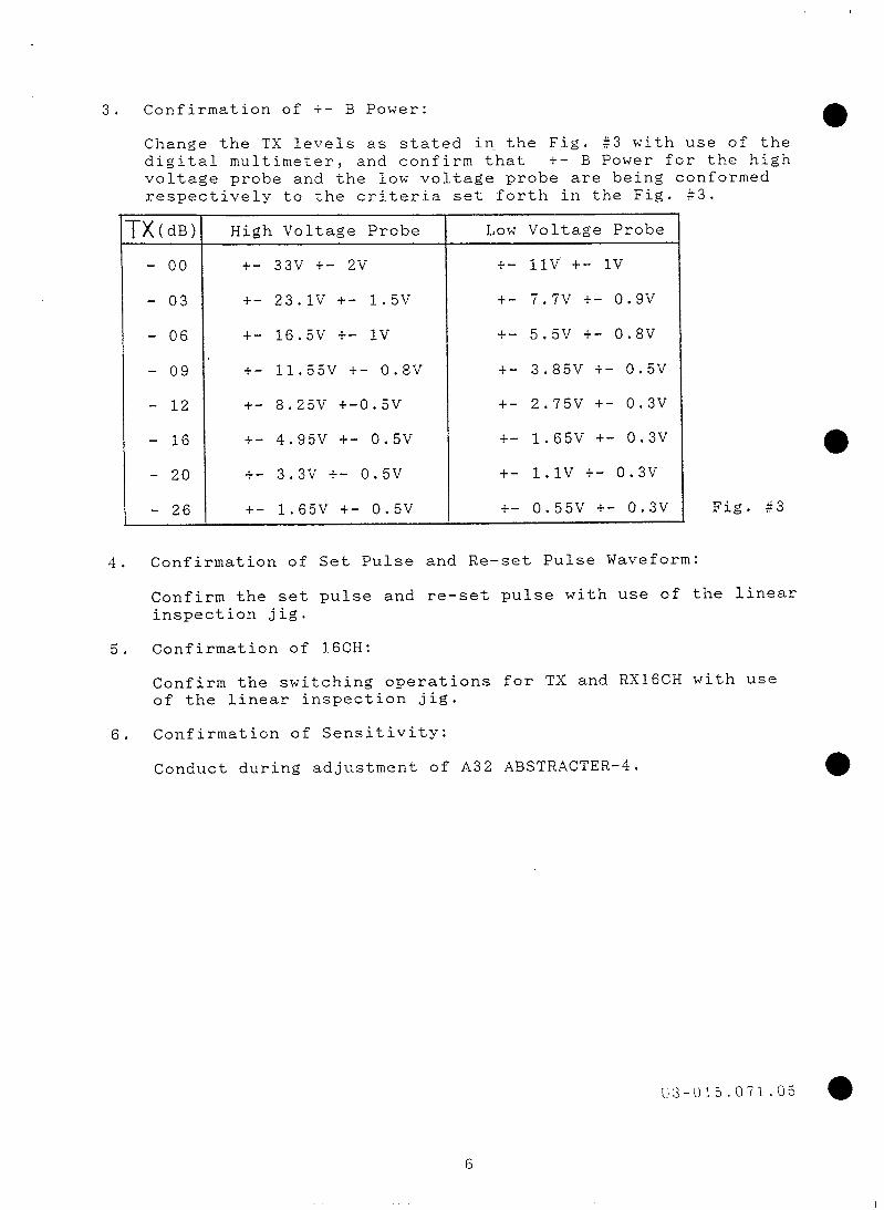
3. Confirmation of +- B Power: a
Change the TX levels as stated in- the Fig. s3 with use of the digital multimeter, and confirm that +- B Power for the high voltage probe and the low voltage probe are being conformed respectively to the criteria set forth in the Fig.
f-X(dW High Voltage Probe Low Voltage Probe
- 00 -I-- 33v t- 2v t- llv' -I-- 1v
- 03 t- 23.1V +- 1.5V t- 7.7v t- 0.9v
- 06 t- 16.5V t- IV -I-- 5.5v t- 0.8V
- 09 t- 11.55V +- 0.8V t- 3.85V -I-- 0.5v
- 12 t- 8.25V t-0.5V t- 2.75V +- 0.3V
- 16 +- 4.95V +- 0.5V +- 1.65V +- 0.3V
- 20 t- 3.3v -I-- 0.5V t- I.lV +- 0.3v
- 26 +- 1.65V t- 0.5V f- 0.55v t- 0.3v Fig. $3
4. Confirmation of Set Pulse and Re-set Pulse Waveform:
Confirm the set pulse and re-set pulse with use of the linear inspection jig.
5. Confirmation of 16CH:
Confirm the switching operations for TX and RXlGCH with use of the linear inspection jig.
6, Confirmation of Sensitivity:
Conduct during adjustment of A32 ABSTRACTER-4.
a
a
6
A32 ABSTRACTER-4 ADJUSTMENT PROCEDURES
0. Heasuring Equipment and Initial Setting:
O-l. Weasuring Equipment:
a. b.
C.
d. e. f. g.
Oscilloscope (200 MHz minimum) Standard Signal Generator (VP-8191A) 50 ohm 1MHz to 1OMHz SINE WAVE 132 dBuV 50 ohm Termination 0.068 uF Capacitor Extended PCB 3.5MHz ABDOMINAL Probe 3.5MHz Linear Probe
o-2. Initial Setting
a. Set after A35 DIGITIZER is adjusted,
b. Extend the A32 PCB with use of the extended PCB, and connect the cable from A31-1 with Jl.
c. Set the volumes R40, R52, R66, R69, R78 & R82 close to the center on the A32 PCB.
d. Turn the RxVR on the A31-1 PCB to left completely.
e. Obtain an external synchronism for the oscilloscope from Pl-30A.
f. Input the figures as shown in the Attachment #4 into the memory of the standard frequency generator.
1. Confirmation of Power Voltage:
l-l. Confirmation of t 12V:
a. Confirm the voltage is being t 12V t- 0.4V.
l-2. Confirmation of - 12V:
a. Confirm the voltage is being - 12V t- 0.4~.
l-2. Confirmatin of +5V:
a. Confirm the voltage is being +5V +- 0.2V.
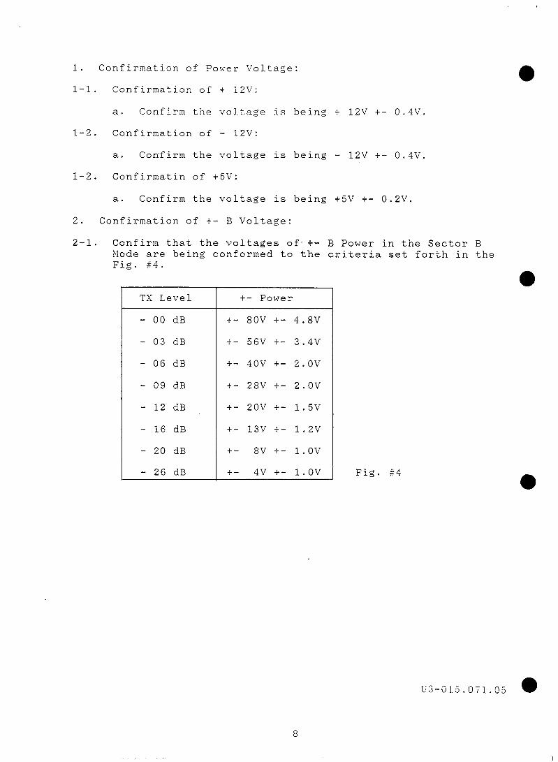
2. Confirmation of t- B Voltage:
2-1. Confirm that the voltages of-+- B Power in the Sector B >lode are being conformed to the criteria set forth in the Fig. $4.
TX Level t- Power
- 00 dB t- 80V t- 4.8V
- 03 dB t- 56V t- 3.4V
- 06 dB t- 4ov t- 2.ov
- 09 dB t- 28V -I-- 2.OV
- 12 dB t- 2ov +- 1.5v
- 16 dB t- 13v +- 1.2v
- 20 dB t- 8V +- l.OV
- 26 dB +- 4v t- l.OV
a
a
Fig. $4 a
~3-015.071.03 a
8
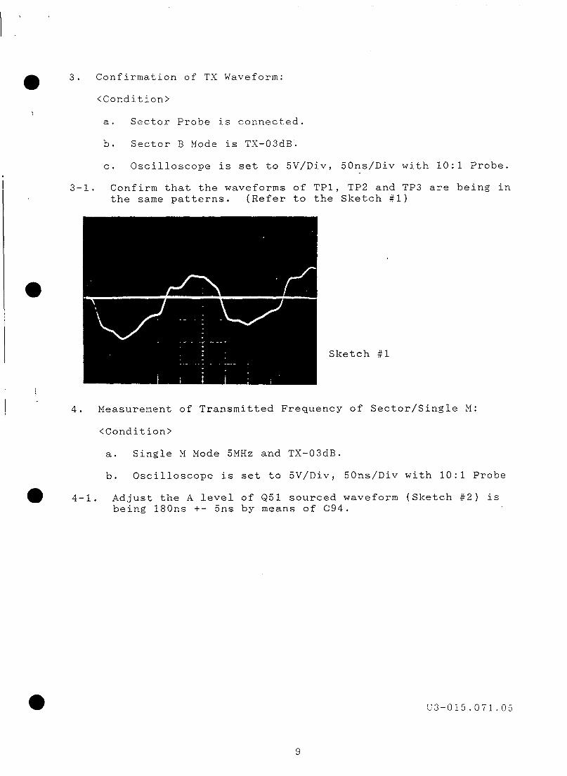
a 3.
3-l
Confirmation of TX Waveform:
<Condition>
a. Sector Probe is connected.
b. Sector B Mode is TX-03dB.
C. Oscilloscope is set to 5V/Div, 50ns/Div with 1O:l Probe.
Confirm that the waveforms of TPl, TP2 and TP3 are being in the same patterns. (Refer to the Sketch Rl)
4.
a 4-l
Measurement of Transmitted Frequency of Sector/S
<Condition>
ingle M:
a. Single M Mode 5MHz and TX-03dB.
b. Oscilloscope is set to 5V/Div, 50ns/Div with 1O:l Probe
Adjust the A level of Q51 sourced waveform (Sketch #2) is being 180ns t- 5ns by means of C94.
9
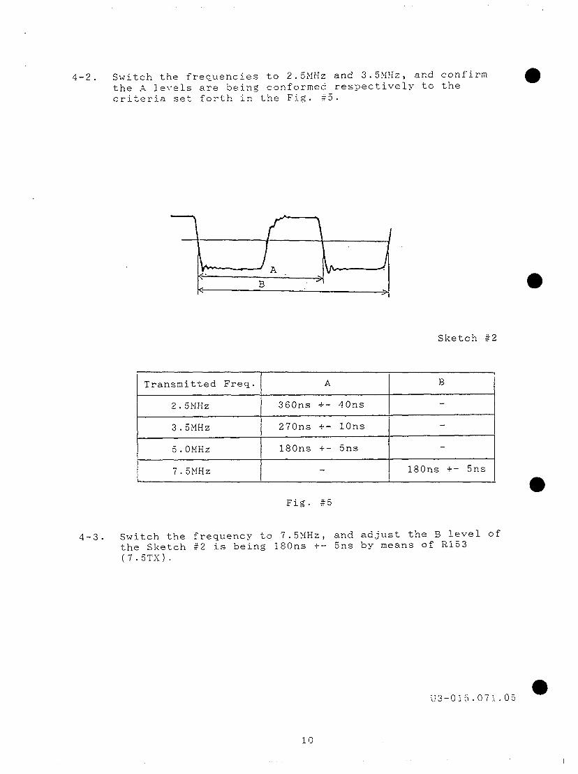
4-2. Switch the frequencies to 2.5NHz and 3.5FiHz, and confirm the A levels are being conformed respectively to the criteria set forth in the Fi$. $5.
Sketch e2
Transmitted Freq. A B
2.5MHz 360ns +- 40ns
3.5MHz 270ns t- 1Ons
5.OMHz 180ns f- 5ns
7.5NHz 180ns t- 5ns 1
Fig. f5
4-3. Switch the frequency to 7.5MH2, and adjust the B level of the Sketch #2 is being 180ns +- 5,s by means of R153 (7.5TX).
u3-015.071.0~ a
10
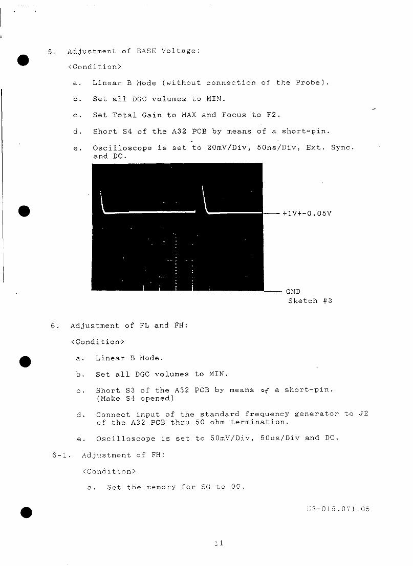
5.
a
Ad.justment of BASE Voltage:
<Condition>
a.
b.
C.
d.
e.
Linear B Mode (without connection of the Probe).
Set all DGC volumes to MIN.
Set Total Gain to MAX and Focus to F2.
Short S4 of the A32 PCB by means of a short-pin.
Oscilloscope is set to 20mV/Div, 50ns/Div, Ext. Sync. and DC.
Sketch $3
6. Adjustment of FL and FH:
<Condition,>
a.
b.
C.
d.
e.
Linear B Mode.
Set all DGC volumes to MIN.
Short S3 of the A32 PCB by means of a short-pin. (Make S4 opened)
Connect input of the standard frequency generator to 52 of the A32 PCB thru 50 ohm termination.
Oscilloscope is set to 50mV/Div, SOus/Div and DC.
6-l. Adjustment of FH:
<Condition>
a. Set the memory for SG to 00.
U3-015.071.05
11
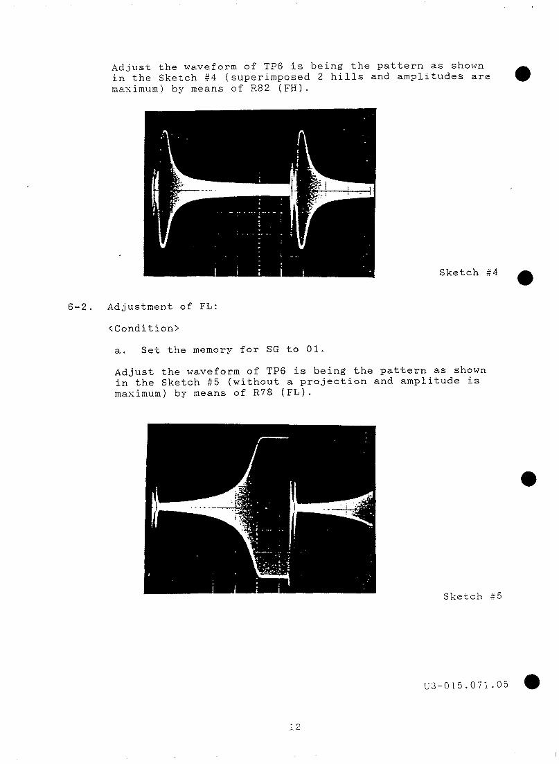
Adjust the waveform of TP6 is being the pattern as shown in the Sketch $4 (superimposed 2 hills and amplitudes are a masimum) by means of R82 (FH).
Sketch $4 0
6-2. Adjustment of FL:
<Condition>
a. Set the memory for SG to 01.
Adjust the waveform of TP6 is being the pattern as shown in the Sketch #5 (without a projection and amplitude is maximum) by means of R78 (FL).
Sketch $5
12
a 6-3.
6-4.
6-5. Set the Single M Mode to 7.5>lHz.
6-6. Adjustment of 7.5NHz FH:
6-7. Adjustment of 7.5MHa FL:
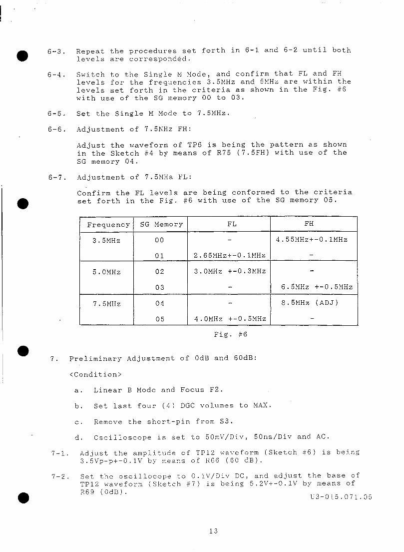
Confirm the FL levels are being conformed to the criteria set forth in the Fig. $6 with use of the SG memory 05.
0 7.
Repeat the procedures set forth in 6-1 and 6-2 until both levels are corresponded.
Switch to the Single M Mode, and confirm that FL and FH levels for the frequencies 3.5MHz and 5MHz are within the levels set forth in the criteria as shown in the Fig. $6 with use of the SG memory 00 to 03.
Adjust the waveform of TP6 is being the pattern as shown in the Sketch +4 by means of R75 (7.5FH) with use of the SG memory 04.
Frequency SG Memory
3.5MHz
5.0MHz
7.5MHz
FL FH
00 4.55MHz+-O.lMHz
01 2.65XHz+-O.lMHz
02 3.0MHz t-0.3MHz
03 6.5MHz I--0.5MHz
04 8.5MHz (ADJ)
05 4.0MHz t-0.5MHz I
Fig. $6
Preliminary Adjustment of OdB and 60dB:
<Condition>
a. Linear B Mode and Focus F2.
b. Set last four (4) DGC volumes to MAX.
C. Remove the short-pin from 53.
d. Oscilloscope is set to 50mV/Div, 50ns/Div and AC.
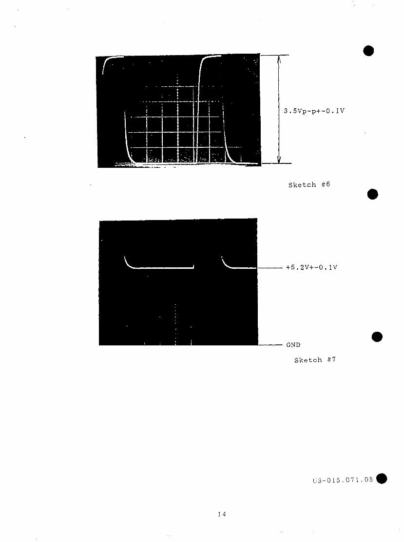
‘7 , I-I. Adjust the amplitude of TP12 waveform (Sketch $6) is being
3.5Vp-P-I--O.lV by means of R66 (60 dB).
7-2. Set the oscillocope to O.lV/Div DC, and adjust the base of TP12 waveform (Sketch +7) is being 5.2Vt-O.lV by means of R69 (OdB).
L3-015.071.05
13
a
3.5Vp-pt-O.lV
14
I
I ’ I .
i
I
a
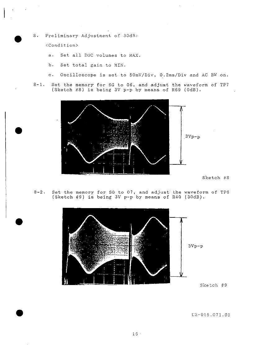
8. Preliminary Adjustment of 30dB:
<Condition>
a. Set all DGC volumes to MAX.
b. Set total gain to MIN.
C. Oscilloscope is set to 50mV/Div, O..2ms/Div and AC BW on.
8-1. Set the memory for SG to 06, and adjust the waveform of TP7 (Sketch #8) is being 3V p-p by means of R69 (OdB).
.3VF+P
Sketch $8
8-2. Set the memory for SG to 07, and adjust‘the waveform of TP6 (Sketch $9) is being 3V p-p by means of R40 (30dB).
3VP-P
Sketch $9
u3-015.071.05
15.
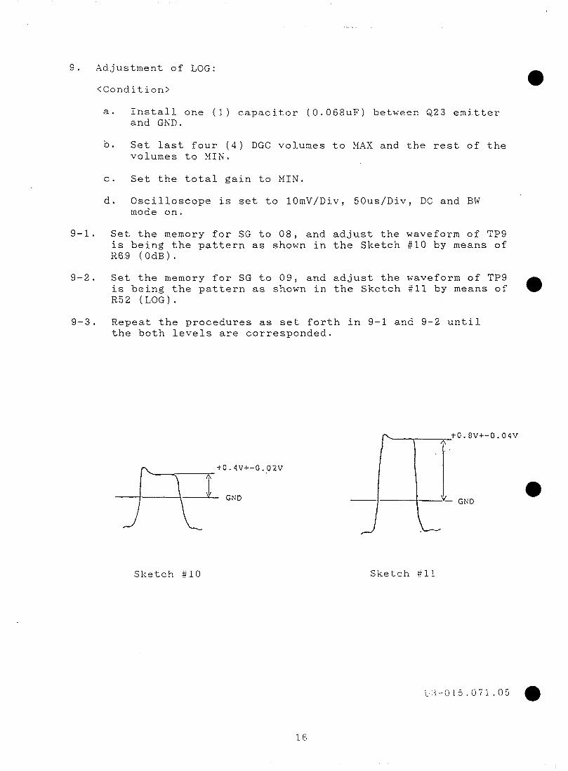
9. Adjustment of LOG:
<Condition>
a. Install one (1) capacitor (0.068uF) between Q23 emitter and GND.
b. Set last four (4) DGC volumes to MAX and the rest of the volumes to MIN.
C. Set the total gain to MIN.
d. Oscilloscope is set to lOmV/Div, SOus/Div, DC and BW mode on.
9-1. Set the memory for SG to 08, and adjust the waveform of TP9 is being the pattern as shown in the Sketch ~$10 by means of R6.9 (OdB).
9-2. Set the memory for SG to 09, and adjust the waveform of TP9 is being the pattern as shown in the Sketch #ll by means of R52 (LOG).
9-3. Repeat the procedures as set forth in 9-1 and 9-2 until the both levels are corresponded.
Sketch $10
t0.8V+-0.04V \
A .
i Q - GND
Sketch #13
16
10. Adjustment of 30dB:
<Condition>
a. Remove the capacitor installed between Q23 emitter and GND.
b. Set all DGC volumes to MAX and the total gain to MIN.
C. Oscilloscope is set to 50mV/Div, D.2ms/Div, AC and BW mode on.
10-l. Select one (1) memory for the waveform of TP7 which is most close to the Sketch $8 (close to 3V p-p) out of the memories 11 through 14.
10-2. Adjust the waveform of TP7 is being 3V p-p by means of R69 (.OdB) .
10-3. Change the SG with the memories corresponding with the current memories. (Use LEVEL PRESET)
Current Memory LEVEL PRESET
11 ------ > a
12 se---- > b
13 em---- > C
14 ------ > d
10-4. Adjust the waveform of TP6 is being 0.3Vp-p by means of R40 (30dB).
11. Adjustment of OdB and 60dB:
<Condition>
a. A Mode on Linear B Mode, FOV is 16cm, AC and BW mode on. Correlation is 50% and DR45, EE2.
b. Oscilloscope is set to 5mV/Div, 0.2ms/Div and AC BW on.
C. Focus is F2.
11-l. Set TEXT mode "ON", and display a minus mark 11-11 on the position as shown in the Sketch #12.
U3-015.071.05
17
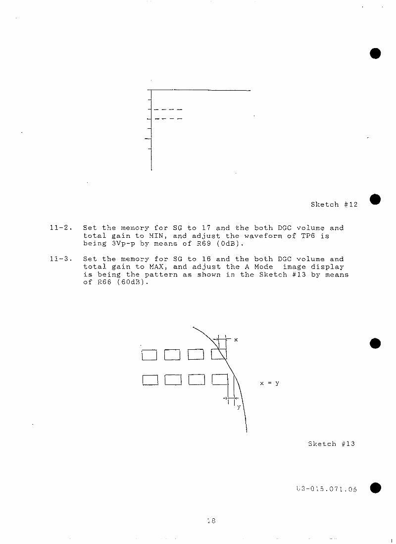
Sketch $12
11-2. Set the memory for SG to 17 and the both DGC volume and total gain to MIN, and adjust the waveform of TP6 is being 3Vp-p by means of R69 (OdB).
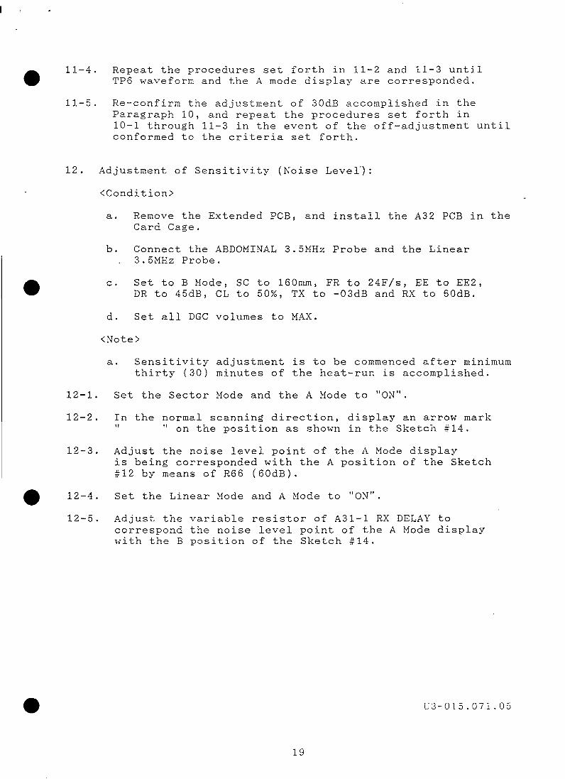
11-3. Set the memory for SG to 16 and the both DGC volume and total gain to MAX, and adjust the A Mode image display is being the pattern as shown in the Sketch #13 by means of R66 (60dB).
x = y
Sketch 313
li3-0 15 . 07 1 . 05 a
18
11-4. Repeat the procedures set forth in 11-2 and 11-3 until TP6 waveform and the A mode display are corresponded.
11-5. Re-confirm the adjustment of 30dB accomplished in the Paragraph 10, and repeat the procedures set forth in 10-l through 11-3 in the event of the off-adjustment until conformed to the criteria set forth.
12. Adjustment of Sensitivity (Noise Level.'):
<Condition>
a. Remove the Extended PCB, and install the A32 PCB in the Card Cage.
b. Connect the ABDOMINAL 3.5MHz Probe and the Linear . 3.5MHz Probe.
C. Set to B Mode, SC to 160mm, FR to 24F/s, EE to EE2, DR to 45dB, CL to 50%, TX to -03dB and RX to 60dB,
d. Set all DGC volumes to MAX.
<Note>
12-1.
12-2.
12-3.
a 12-4.
12-5.
a. Sensitivity adjustment is to be commenced after minimum thirty (30) minutes of the heat-run is accomplished.
Set the Sector Mode and the A Mode to "ON".
In the normal scanning direction, display an arrow mark 11 ( on the position as shown in the Sketch $14.
Adjust the noise level point of the A Mode display is being corresponded with the A position of the Sketch #12 by means of R66 (60dB).
Set the Linear Mode and A Mode to "ON".
Adjust the variable resistor of A31-1 RX DELAY to correspond the noise level point of the A Mode display with the B position of the Sketch #14.
L3-015.071.05
19
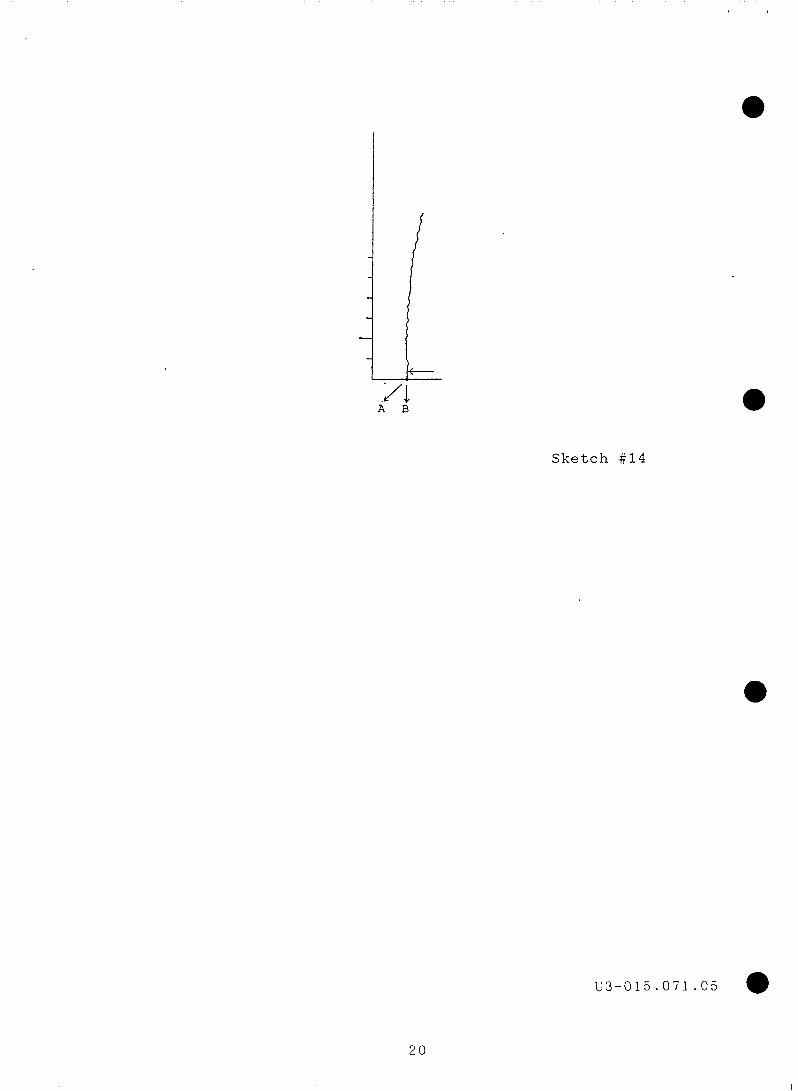
Sketch #14
Ij3-01~.071.05 a
20
Appendix
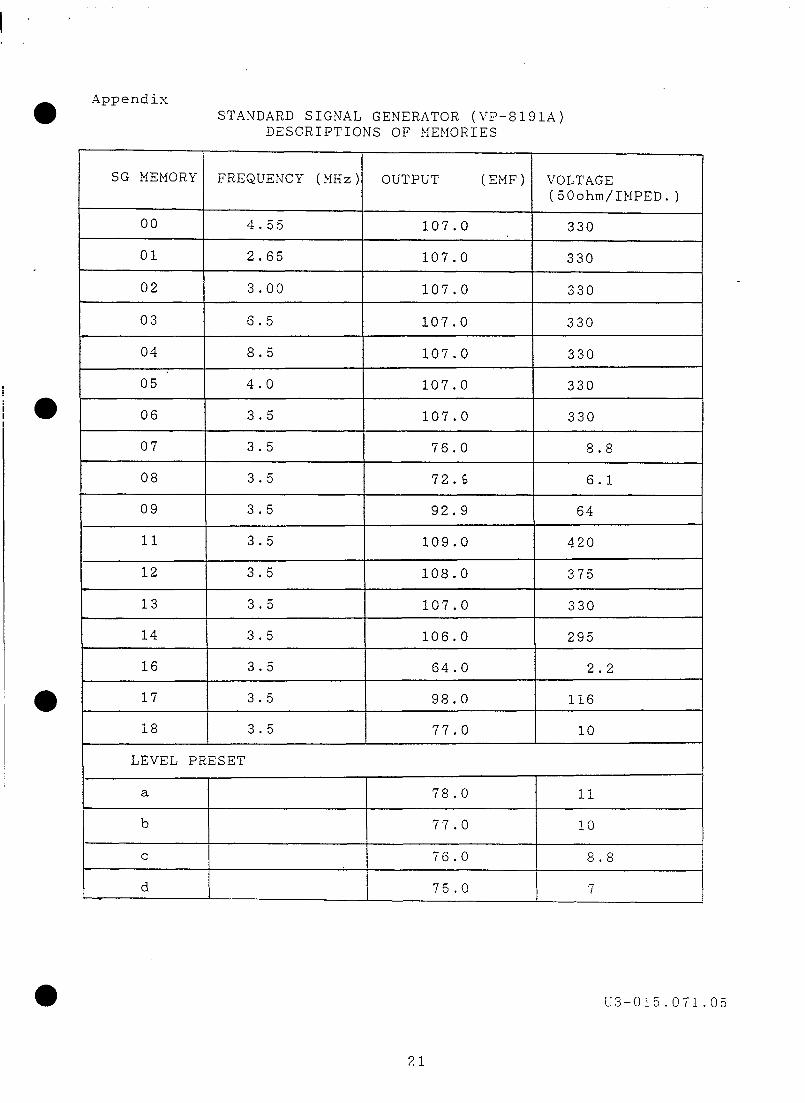
SG MEMORY
03 I-- 04
I 05 ’
11
12
I 13
I 18
STANDARD SIGNAL GENERATOR (VP-8191A) DESCRIPTIONS OF MEMORIES
FREQUENCY (MHz) OUTPUT (EMF) VOLTAGE (50ohm/IMPED.)
4.55 107.0 330
2.65 107.0 330
3.00 107.0 330
6.5 107.0 330
8.5 107.0 330
4.0 107.0 330
3.5 107.0 330
3.5 76.0 8.8
3.5 72.6 6.1
3.5 92.9 64
3.5 109.0 420
3.5 108.0 375
3.5 107.0 330
3.5 106.0 295
3.5 64.0 2.2
3.5 98.0 116
3.5 77.0 10
LEVEL PRESET
a 78.0 11
b 77.0 10
C 76.0 8.8
d 75.0 7
ti3-015.071.05
21
X33 SECTOR-4 ADJUSTXENT PROCEDURES
0. Xeasuring Equipment and Initial Setting:
O-l. Measuring Equipment:
a. Digital Oscilloscope b. Digital Xultimeter c. Extended PCB d. 3.5HHz Inline D19 Probe
o-2. Initial Setting:
a. Set the short-pins as follows:
1) 53 -----> STD side 2) 54 -----> STDl side
b. In advance, set the variable resistors R23 and R165 to the center positions.
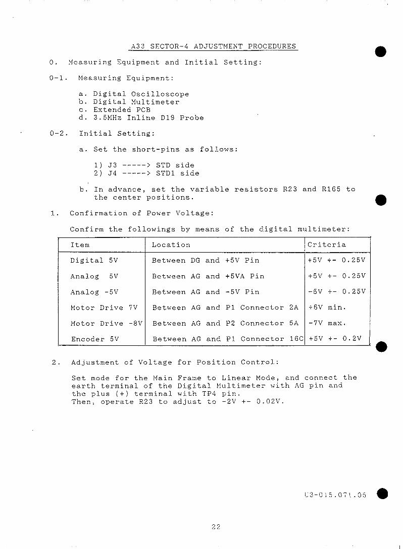
1. Confirmation of Power Voltage:
Confirm the followings by means of the digital multimeter:
Item Location Criteria
Digital 5V Between DG and +5V Pin t5V t- 0.25V
Analog 5V Between AG and +5VA Pin 15V +- 0.25V
Analog -5V Between AG and -5V Pin -5V +- 0.25V
Motor Drive 7V Between AG and Pl Connector 2A t6V min.
Motor Drive -8V Between AG and P2 Connector 5A -7V max.
Encoder 5V Between AG and Pl Connector 16C +5V t- 0.2V
2. Adjustment of Voltage for Position Control:
Set mode for the Main Frame to Linear Mode, and connect the earth terminal of the Digital Multimeter with AG pin and the plus (t) terminal with TP4 pin. Then, operate R23 to adjust to -2V t- 0.02V.
a
c3-015.071.05 a
22
! I
a 3. Position Control Off-Set Voltage:
Connect the earth terminal of the Digital Multimeter with AG pin and the plus (i) terminal with the center terminal of R165. Connect the 3.5MHz Inline Sector D19 Probe. After stopped the rotor by means of Sector M Mode, then operate R165 to adjust to 0 t- O.OlV.
ti3-015.071.05
23
A34 SUPERVISOR-Z ADJUSTMENT PROCEDURES
0. Measuring Equipment:
a. Frequency Counter (8 digits)
1. Adjustment of Clock Frequency:
a. At the Test Pin lHz, adjust Cl4 Clock to conform to the criteria of 0.999995 set to 1.000005 sec.
b. In the event of not conformed to the criteria, adjust C42 by means of the capacitor in the range of 39pF to 68pF.
c. In the event of no adjustment is made with above step b, replace the crystal.
2. Adjustment of CPU Clock:
a. At U37 (CPUSOCSS) 19 Pin, adjust C5 for the frequency is being 3.3MHz f- 0.005MHz.
L3-01~.071.05 0
24
A35 DIGITIZER PCB ADJUSTMENT PROCEDURES
a 0. Measuring Equipment and Initial Setting:
o-1. Measuring Equipment:
a. DIGITIZER Adjustment Jig b. Extended PCB c. Digital Multimeter d, Oscilloscope (100MHz min.)
o-2. Initial Setting:
a. Pull the A35 DIGITIZER PCB, and extend with use of the Extended PCB. Detach A32 ABSTRACTER-4 PCB.
b Connect the cables from the DIGITIZER Adjustment Jig ' with Pl-32C and GND.
c. Connect CHl of the Oscilloscope with U48 89 Pin.
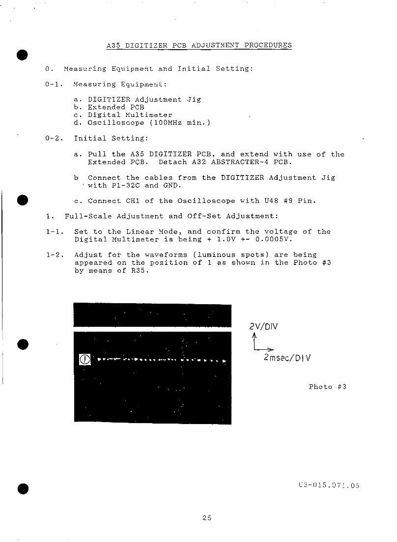
1. Full-Scale Adjustment and Off-Set Adjustment:
l-l. Set to the Linear Mode, and confirm the voltage of the Digital Multimeter is being t l.OV +- 0.0005V.
l-2. Adjust for the waveforms (luminous spots) are being appeared on the position of 1 as shown in the Photo #3 by means of R35.
2V/DIV
L 2mszc/Dl V
Photo $3
u3-015.071.05
25
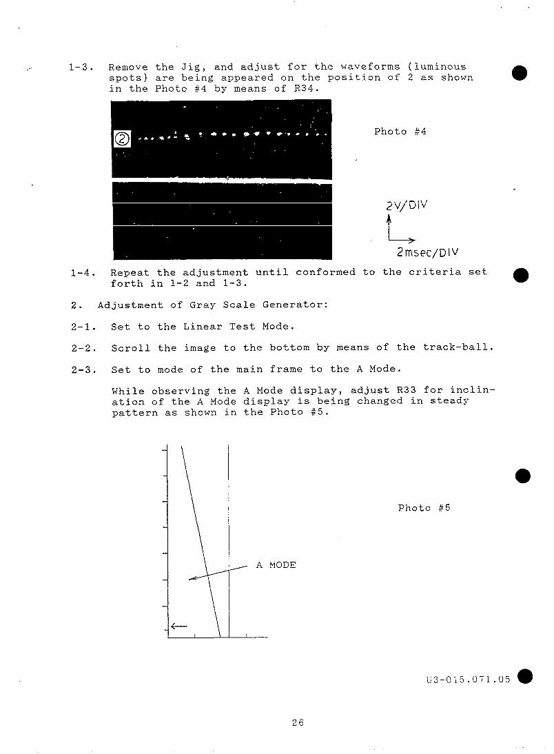
1-3. Remove the Jig, and adjust for the waveforms (luminous spots) are bein g appeared on the position of 2 as shown in the Photo $4 by means of R34.
Photo $4
2V/DIV
L 2msec/Dlv
l-4, Repeat the adjustment until conformed to the criteria set forth in l-2 and l-3.
2. Adjustment of Gray Scale Generator:
2-l. Set to the Linear Test Mode.
2-2. Scroll the image to the bottom by means of the track-ball.
2-3. Set to mode of the main frame to the A Mode.
While observing the A Mode display, adjust R33 for inclin- ation of the A Mode display is being changed in steady pattern as shown in the Photo #5.
Photo $5
, A MODE
26
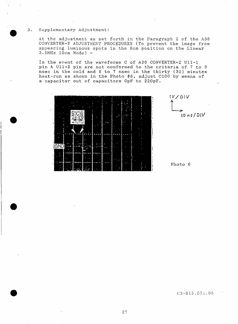
a 3. Supplementary Adjustment:
At the adjustment as set forth in the Paragraph 2 of the A36 CONVERTER-2 ADJUSTMENT PROCEDURES (To prevent the image from appearing luminous spots in the 8cm position on the Linear 3.5MHz 1Ocm Mode) -
In the event of the waveforms C of A36 CONVERTER-2 Ull-1 pin 6: Ull-2 pin are not conformed to the criteria of 7 to 9 nsec in the cold and 5 to 7 nsec in the' thirty (30) minutes heat-run as shown in the Photo $6, adjust Cl00 by means of a capacitor out of capacitors OpF to 220pF.
I 0 I !
(0 MS/ OIL’
Photo 6
U3-01~.071.05
27
A36 CONVERTER-2 ADJUSTMENT PROCEDURES
0.
1.
Measuring Equipment:
a. Oscilloscope (100MHz min.)
Supplementary Adjustment 1:
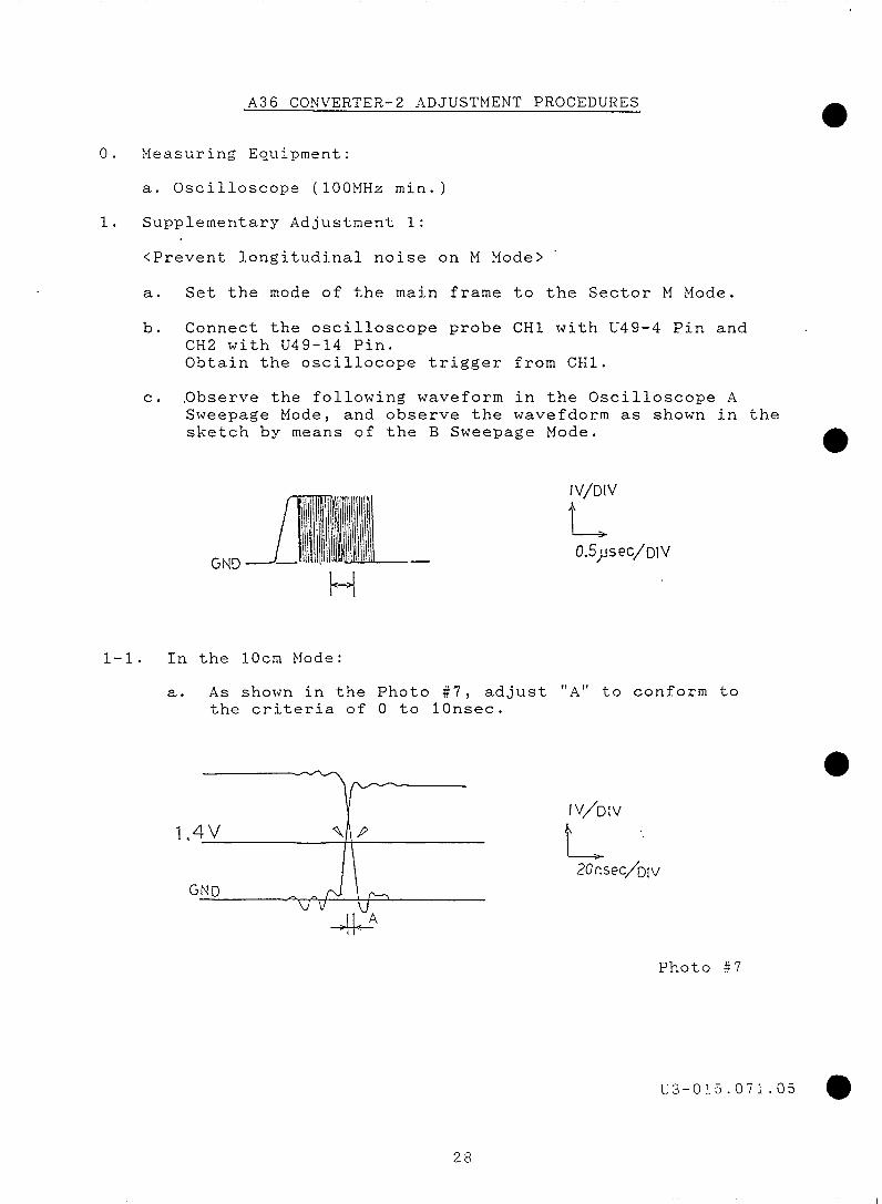
<Prevent longitudinal noise on M Mode> '
a. Set the mode of the main frame to the Sector M Mode.
b. Connect the oscilloscope probe CHl with U49-4 Pin and . CH2 with U49-14 Pin. Obtain the oscillocope trigger from CHl.
C. .Observe the following waveform in the Oscilloscope A Sweepage Mode, and observe the wavefdorm as shown in the sketch by means of the B Sweepage Mode.
GND -
k-4
IV/Oh’
f 0.5psec/D1V
l-1. In the 1Ocm Mode:
a. As shown in the Photo #7, adjust "A" to conform to the criteria of 0 to 10nsec.
II 20nsec/&v
GND I, vv
A -4-k
Photo $7
28
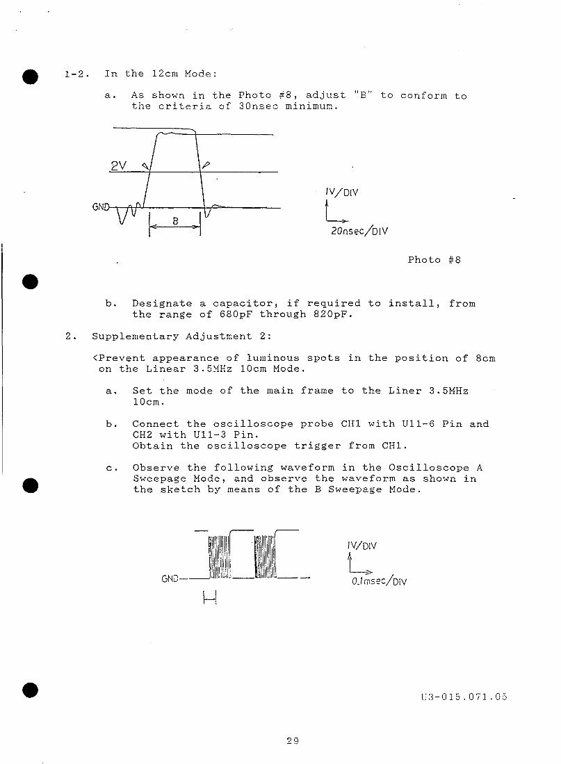
a 1-2. In the 12cm Mode:
a. As shown in the Photo $8, adjust "B" to conform to the criteria of 30nsec minimum.
ZOnsec/DIV
Photo #8
b. Designate a capacitor, if required to install, from the range of 680pF through 820pF.
2. Supplementary Adjustment 2:
<Prevent appearance of luminous spots in the position of 8cm on the Linear 3.5MHz 1Ocm Mode.
a. Set the mode of the main frame to the Liner 3.5MHz 10cm.
b. Connect the oscilloscope probe CHl with Ull-6 Pin and CH2 with Ull-3 Pin. Obtain the oscilloscope trigger from CHl.
C. Observe the following waveform in the Oscilloscope A Sweepage Mode, and observe the waveform as shown in the sketch by means of the B Sweepage Mode.
U3-015.071.05
29
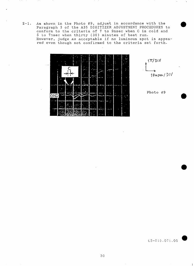
2-1. As shown in the Photo +!9, adjust in accordance with the Paragraph 3 of the A35 DIGITIZER ADJUSTMENT PROCEDURES to a conform to the criteria of 7 to Snsec when C is cold and 5 to 7nsec when thirty (30) minutes of heat run. However, judge as acceptable if no luminous spot is appea- red even though not confirmed to the criteria set forth.
Photo 99 a
a
L3-015.071.05 a
30
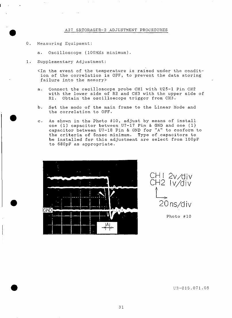
a A37 SRTORAGER-2 ADJUSTMENT PROCEDURES
0. Measuring Equipment:
a. Oscilloscope (100MHz minimum).
1. Supplementary Adjustment:
<In the event of the temperature is raised under the condit- ion of the correlation is OFF, to prevent the data storing failure into the memory>
a. Connect the oscilloscope probe CHl with U25-1 Pin CH2 with the lower side of R2 and CH3 with the upper side of Rl. Obtain the oscilloscope trigger from CH3.
a
b. Set the mode of the main frame to the Linear Mode and the correlation to OFF.
C. As shown in the Photo #lo, adjust by means of install one (1) capacitor between U7-17 Pin & GND and one (1) capacitor between U7-18 Pin & GND for "A" to conform to the criteria of Snsec minimum. Type of capacitors to be installed for this adjustment are select from 1OOpF to 680pF as appropriate.
U3-015.071.05
31
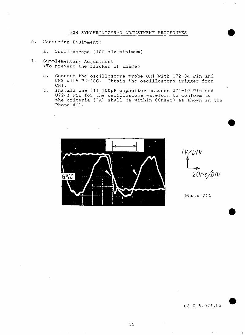
A38 SYNCHRONIZER-2 ADJUSTMENT PROCEDURES a
0. Measuring Equipment:
a. Oscilloscope (100 MHz minimum)
1. Supplementary Adjustment: <To prevent the flicker of image>
a. Connect the oscilloscope probe CHl 'with U72-34 Pin and CH2 with P2-28C. Obtain the oscilloscope trigger from CHl.
b. Install one (1) 1OOpF capacitor between U74-10 Pin and U72-1 Pin for the oscilloscope waveform to conform to the criteria ("A" shall be within 60nsec) as shown in the Photo gll.
a
I V/Ill v
L 209/6/v
Photo #ll
a
C3-015.071.05 a
32
Y
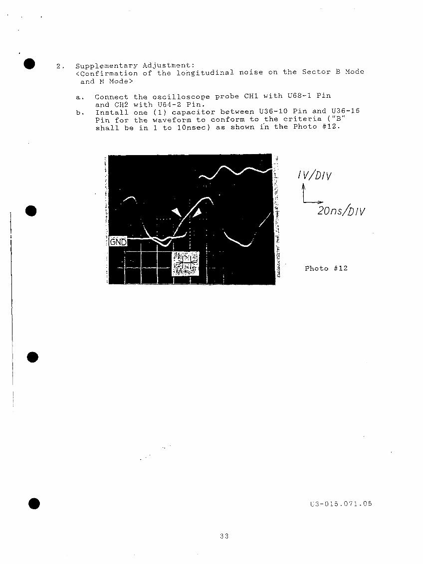
a 2. Supplementary Adjustment: <Confirmation of the longitudinal noise on the Sector B Mode
and M Mode>
a. Connect the oscilloscope probe CHl with U68-1 Pin and CH2 with U64-2 Pin.
b. Install one (1) capacitor between U36-10 Pin and U36-15 Pin for the waveform to conform to the criteria ("B" shall be in 1 to 10nsec) as shown Ln the Photo +12.
j a I I
I V/D/v
L 20f7s/bIV
Photo if12
L3-015.071.05
33
A40 IMAGER-2 ADJUSTMENT PROCEDUR,ES
0. Measuring Equipment:
a. Standard TV Signal Generator (CCIR or NTSC) b. Frequency Counter
1. Adjustment of Playback Clock:
a. Connect the Standard TV Signal Generator with the "VIDEO INPUT" of the Rear Panel.
b. Then, set to the playback mode,of the main frame, and connect the Frequency Counter with TP3.
C. Adjust to 11.32 f- 0.03MHz by means of R33.
a
u3-015.071.03 a
34
I
.4PPESDIS:
HANDLING SEQUENCE FOR ADJUSTMENT PROCEDURES FOR DIGITAL SECTION
Adjust as per the following sequences. (A34 SUPERVISOR-2, A35 DIGITIZER, A36 CONVERTER-2, A37 STORAGER- 2, A38 SYNCHRONIZER-2 and A40 IMAGER-2)
SEQ. 1
A40 IMAGER-2 PCB (A40 1. on page 34) <SEQUENCE> Adjust as shown in A40 1. on page 34. <PURPOSE> To adjust playback clock.
SEQ. 2
A34 SUPERVISOR-2 PCB (A34 1. and 2. on page 24) <SEQUENCE> Adjust as shown in A34 1. and 2. on page 24. <PURPOSE> To adjust playback clock.
SEQ. 3
A35 DIGITIZER PCB (A35 1. and 2. on page 25 and 26) <SEQUENCE> Adjust as shown in A35 1. and 2. on page 25 and 26. <PURPOSE> To adjust full-scale, off-set and gray scale generator.
SEQ. 4
A38 SYNCHRONIZER-2 PCB (A38 1. on page 32) <SEQUENCE> Confirm the timing (Photo #ll on page 32) in LINEAR B mode. In case of not conformed to the timing, install one (1) capacitor as shown in A38 1. on page 32. <PURPOSE> To prevent the image from flickering.
SEQ. 5
A38 SYNCHRONIZER-2 PCB (A38 2. on page 33) <SEQUENCE> Confirm the timing (Photo #12 on page 33). In case of not conformed to the timing, install one (1) capacitor as shown in A38 2. on page 33. <PURPOSE> To prevent the longitudinal noise of SECTOR B mode and M mode image.
U3-015.071.05
SEQ. 6
A36 CONVERTER-2 PCB (~36 1. on page 28 and 29) <SEQUENCE> Confirm the timing (~36 1. on page 28 and 29). In case of not conformed to the timing, install one (1) capacitor between 13 pin of U38 (LS04) and GND. <PURPOSE> To prevent the longitudinal noise of M mode image.
SEQ. 7
A36,CONVERTER-2 PCB (A36 2. on page 29 and 30) A35 DIGITIZER PCB (A35 3. on page 27) <SEQUENCE> Confirm the timing (A36 2. on page 29 and 30). In case of not conformed to the timing, adjust Cl00 by means of a capacitor out of OpF to 220pF as shown in A35 3. on page 27. <PURPOSE> To prevent the image from appearing luminous spots in the 8cm position on the LINEAR 3.5MIIz 1Ocm mode.
SEQ. 8
A37 STORAGER-2 PCB (A37 1. on page 31) <SEQUENCE> Confirm the timing (Photo #lo on page 31). In case of not conformed to the timing, install two (2) capacitors as shown in A37 1. on page 31. <PURPOSE> In the event of the temperature is raised under the condition of the correlation is OFF in TEST PATTERN mode, to prevent luminous spots in the image.
36
a
U3-015.071.05