Embed Size (px)
Citation preview
Structure and morphology ofultrathin iron and iron oxide �lms on
Ag(001)
Dissertation
zur Erlangung des Grades einesDoktors der Naturwissenschaften (Dr. rer. nat.)
dem Fachbereich Physik der Universität Osnabrückvorgelegt von
Daniel Bruns, Dipl. Phys.
Osnabrück, Oktober 2012


In science there are no 'depths';there is surface everywhere.
- Dr. phil. Rudolf Carnap (1891 - 1970)

Contents
1 Introduction 1
2 Theoretical background 3
2.1 Crystal structures . . . . . . . . . . . . . . . . . . . . . . . . . . . . . . . . . 3
2.1.1 Bulk lattices . . . . . . . . . . . . . . . . . . . . . . . . . . . . . . . 3
2.1.2 Surface lattices . . . . . . . . . . . . . . . . . . . . . . . . . . . . . . 4
2.1.3 Growth modes . . . . . . . . . . . . . . . . . . . . . . . . . . . . . . 5
2.2 Low Energy Electron Di�raction . . . . . . . . . . . . . . . . . . . . . . . . 7
2.2.1 Kinematic theory of electron di�raction . . . . . . . . . . . . . . . . 8
2.2.2 Atomically stepped surfaces . . . . . . . . . . . . . . . . . . . . . . . 11
2.2.3 H(S) analysis . . . . . . . . . . . . . . . . . . . . . . . . . . . . . . . 13
2.2.4 Two dimensional model in H(S) analysis . . . . . . . . . . . . . . . . 14
2.2.5 Mosaics and facets . . . . . . . . . . . . . . . . . . . . . . . . . . . . 15
2.2.6 Superstructures and undulations . . . . . . . . . . . . . . . . . . . . 18
2.2.7 G(S) analysis . . . . . . . . . . . . . . . . . . . . . . . . . . . . . . . 22
2.3 X-ray Photoelectron Spectroscopy . . . . . . . . . . . . . . . . . . . . . . . 25
2.3.1 The photoelectrical e�ect . . . . . . . . . . . . . . . . . . . . . . . . 26
2.3.2 Photoemisson spectra . . . . . . . . . . . . . . . . . . . . . . . . . . 27
2.4 Auger Electron Spectroscopy . . . . . . . . . . . . . . . . . . . . . . . . . 29
2.5 Quantitative XPS and Auger analysis . . . . . . . . . . . . . . . . . . . . . 31
2.6 Scanning Tunneling Microscopy . . . . . . . . . . . . . . . . . . . . . . . . 34
2.6.1 The one dimensional tunneling e�ect . . . . . . . . . . . . . . . . . . 35
2.6.2 Tersoff-Harmann-approximation . . . . . . . . . . . . . . . . . . 36
2.6.3 Topographic height measurements in STM . . . . . . . . . . . . . . . 37
3 Material system 41
3.1 The substrate - Ag(001) . . . . . . . . . . . . . . . . . . . . . . . . . . . . . 41
3.2 The adsorbates . . . . . . . . . . . . . . . . . . . . . . . . . . . . . . . . . . 42
3.2.1 Iron . . . . . . . . . . . . . . . . . . . . . . . . . . . . . . . . . . . . 43
3.2.2 FeO - wustite . . . . . . . . . . . . . . . . . . . . . . . . . . . . . . . 45
3.2.3 Fe3O4 - magnetite . . . . . . . . . . . . . . . . . . . . . . . . . . . . 46
3.2.4 Fe2O3 - maghemite and hematite . . . . . . . . . . . . . . . . . . . . 46
3.2.5 Lattice mismatch between Ag(001) and the adsorbates . . . . . . . . 47
4 Experimental setup 49
4.1 The UHV chambers . . . . . . . . . . . . . . . . . . . . . . . . . . . . . . . 49
4.2 SPA-LEED and LEED . . . . . . . . . . . . . . . . . . . . . . . . . . . . . . 50
4.3 Scanning Tunneling Microscope (STM) . . . . . . . . . . . . . . . . . . . . . 51
4.4 AES . . . . . . . . . . . . . . . . . . . . . . . . . . . . . . . . . . . . . . . . 52
4.5 XPS . . . . . . . . . . . . . . . . . . . . . . . . . . . . . . . . . . . . . . . . 53
4.6 The evaporator . . . . . . . . . . . . . . . . . . . . . . . . . . . . . . . . . . 54
4.7 Sample preparation . . . . . . . . . . . . . . . . . . . . . . . . . . . . . . . . 54
5 Experimental results and discussion 57
5.1 The prepared Ag(001) substrates . . . . . . . . . . . . . . . . . . . . . . . . 57
5.2 Ag(001) substrates Ar+ etched at RT . . . . . . . . . . . . . . . . . . . . . . 62
5.3 Post deposition annealing of Fe �lms on Ag(001) in UHV . . . . . . . . . . 63
5.3.1 As deposited Fe �lms on Ag(001) . . . . . . . . . . . . . . . . . . . . 63
5.3.2 Annealing in UHV . . . . . . . . . . . . . . . . . . . . . . . . . . . . 67
5.3.3 Discussion . . . . . . . . . . . . . . . . . . . . . . . . . . . . . . . . . 75
5.4 Post deposition annealing of Fe �lms on Ag(001) in O2 atmosphere . . . . . 79
5.4.1 Annealing of very low Fe coverages in O2 atmosphere . . . . . . . . . 79
5.4.2 Electron di�raction . . . . . . . . . . . . . . . . . . . . . . . . . . . . 80
5.4.3 Scanning Tunneling Microscopy . . . . . . . . . . . . . . . . . . . . . 82
5.4.4 Discussion . . . . . . . . . . . . . . . . . . . . . . . . . . . . . . . . . 86
5.5 Reactive deposition of Fe on Ag(001) in O2 atmosphere . . . . . . . . . . . 91
5.5.1 X-Ray Photoelectron Spectroscopy . . . . . . . . . . . . . . . . . . . 92
5.5.2 Electron di�raction . . . . . . . . . . . . . . . . . . . . . . . . . . . . 93
5.5.3 Scanning Tunneling Microscopy . . . . . . . . . . . . . . . . . . . . . 98
5.5.4 Determination of the undulated islands by atomically resolved STM 99
5.5.5 G(S) analysis of the undulation . . . . . . . . . . . . . . . . . . . . . 103
5.5.6 Discussion . . . . . . . . . . . . . . . . . . . . . . . . . . . . . . . . . 105
6 Conclusion 111
Bibliography 113
List of Figures 121
List of peer-reviewed publications 133
Acknowledgement 134
Introduction
1 Introduction
Iron and iron oxides are of great interest in various �elds of application due to their largevariety of physical and chemical properties. For instance, iron oxides are well known ascatalysts for several chemical reactions as, e.g., selective oxidation or dehydrogenation[1, 2]. One important issue for this application is that the oxidation state of iron is �exibleand may either be Fe2+ or Fe3+. Therefore, iron forms oxides of di�erent stoichiometries asFeO (wustite), Fe3O4 (magnetite) and Fe2O3 (haematite (trigonal) or maghemite (cubic)).
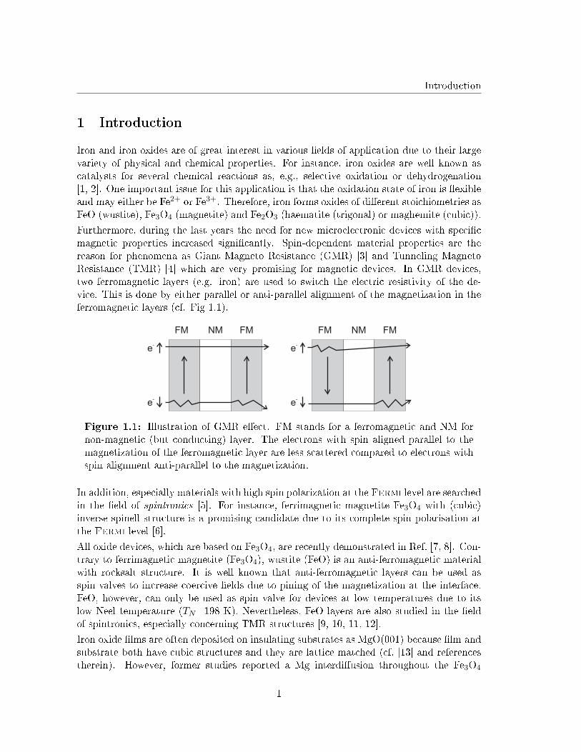
Furthermore, during the last years the need for new microelectronic devices with speci�cmagnetic properties increased signi�cantly. Spin-dependent material properties are thereason for phenomena as Giant Magneto Resistance (GMR) [3] and Tunneling MagnetoResistance (TMR) [4] which are very promising for magnetic devices. In GMR devices,two ferromagnetic layers (e.g. iron) are used to switch the electric resistivity of the de-vice. This is done by either parallel or anti-parallel alignment of the magnetization in theferromagnetic layers (cf. Fig 1.1).
FM FMNM
e-
e-
FM FMNM
e-
e-
Figure 1.1: Illustration of GMR e�ect. FM stands for a ferromagnetic and NM fornon-magnetic (but conducting) layer. The electrons with spin aligned parallel to themagnetization of the ferromagnetic layer are less scattered compared to electrons withspin alignment anti-parallel to the magnetization.
In addition, especially materials with high spin polarization at the Fermi level are searchedin the �eld of spintronics [5]. For instance, ferrimagnetic magnetite Fe3O4 with (cubic)inverse spinell structure is a promising candidate due to its complete spin polarisation atthe Fermi level [6].
All oxide devices, which are based on Fe3O4, are recently demonstrated in Ref. [7, 8]. Con-trary to ferrimagnetic magnetite (Fe3O4), wustite (FeO) is an anti-ferromagnetic materialwith rocksalt structure. It is well known that anti-ferromagnetic layers can be used asspin valves to increase coercive �elds due to pining of the magnetization at the interface.FeO, however, can only be used as spin valve for devices at low temperatures due to itslow Neel temperature (TN=198 K). Nevertheless, FeO layers are also studied in the �eldof spintronics, especially concerning TMR structures [9, 10, 11, 12].
Iron oxide �lms are often deposited on insulating substrates as MgO(001) because �lm andsubstrate both have cubic structures and they are lattice matched (cf. [13] and referencestherein). However, former studies reported a Mg interdi�usion throughout the Fe3O4
1
Introduction
�lms accompanied by a Mg segregation at the surface due to annealing at temperaturesabove 400◦C [14, 15]. This Mg interdi�usion reduces the desired spin polarization of themagnetite �lm.
On the other hand, deposition of iron oxides on metallic substrates has been less investi-gated. This is surprising since there are thorough studies on other transition metal (TM)oxides on various metal substrates (cf. Ref. [13, 16, 17, 18] as well as references therein).One huge exception for epitaxy of iron oxide on metals is the work of Weiss et al. whointensively studied iron oxide epitaxy on Pt(111) [19, 20, 21, 22, 23, 24]. They reportedthat iron oxide always grows initially as FeO(111) layer and that higher oxidation statesare only possible for oxide �lms with �lm thickness beyond a few monolayers. It has to benoted that no �lm-substrate interdi�usion at elevated temperatures was reported for thegrowth of iron oxide on Pt(111).
Nevertheless, using hexagonal substrate surfaces, the formation of (111) oriented FeO �lmsmay not be too surprising. The formation of quasi-hexagonal FeO(111)-like monolayers,however, has also been reported for deposition on fcc(001) surfaces with square symmetryas, e.g., Pt(001) [25, 26] and Cu(001) [27, 28]. Here, FeO forms c(2×10) or (2×9) super-structures on Pt(001) while hexagonal Moiré patterns, due to strain reducing dislocationnetworks, are reported for Cu(001).
Although Lopes et al. investigated the structure of 22 ML FeO(001) �lms on Ag(001) [29],studies on the initial growth of iron oxide layers on Ag(001) are still lacking in literature.This is astonishing, since the lattice mismatch between FeO and Ag is smaller than betweenFeO and other noble metal substrates (e.g. Pt).
Therefore, this work investigates the initial growth of iron and iron oxides on Ag(001).Surface structure and morphology of both post deposition annealed Fe �lms (in UHV andO2 atmosphere) as well as reactive grown iron oxide �lms will be analyzed in detail by lowenergy electron di�raction (LEED) and scanning tunneling microscopy (STM). The stoi-chiometry at the surface of the iron oxide �lms will be determined by X-ray photoelectronspectroscopy (XPS) and Auger electron spectroscopy (AES).
The necessary theoretical background of the techniques as well as the material system usedin this work are introduced in Chap. 2 and Chap. 3, respectively.
In a �rst step, studies on elemental Fe �lms deposited on Ag(001) at RT will be brie�yintroduced. Afterward, the segregation of Ag at the surface of the Fe �lms during UHVannealing will be investigated (Chap. 5.3). This segregation has been reported for mono-layer Fe �lms as atom site exchange in former studies concerning Fe monolayers on Ag(001)[30, 31]. Here, we will concentrate on the changes in surface structure that my be causedby the Ag segregation, since this is still lacking in literature.
However, the main focus of this work is to shed light on the question whether the growth ofiron oxide �lms on Ag(001) is accompanied by the formation of strain reducing dislocationnetworks, or superstructures as found for other metal substrates in former studies [25, 26,27, 28]. Here, we will distinguish between Fe �lms which were post deposition annealed ina thin O2 atmosphere (Chap. 5.4) and reactively grown iron oxide �lms (Chap. 5.5).
2
Theoretical background
2 Theoretical background
In this section the theory of crystal lattices and the theoretical background concerning theexperimental methods used in this work will be introduced.
2.1 Crystal structures
The main objective of this work is the investigation of structure and morphology of ultrathin crystalline iron oxide �lms. Therefore, it is useful to �rst give a brief introduction tothree and two dimensional crystal lattices.
2.1.1 Bulk lattices
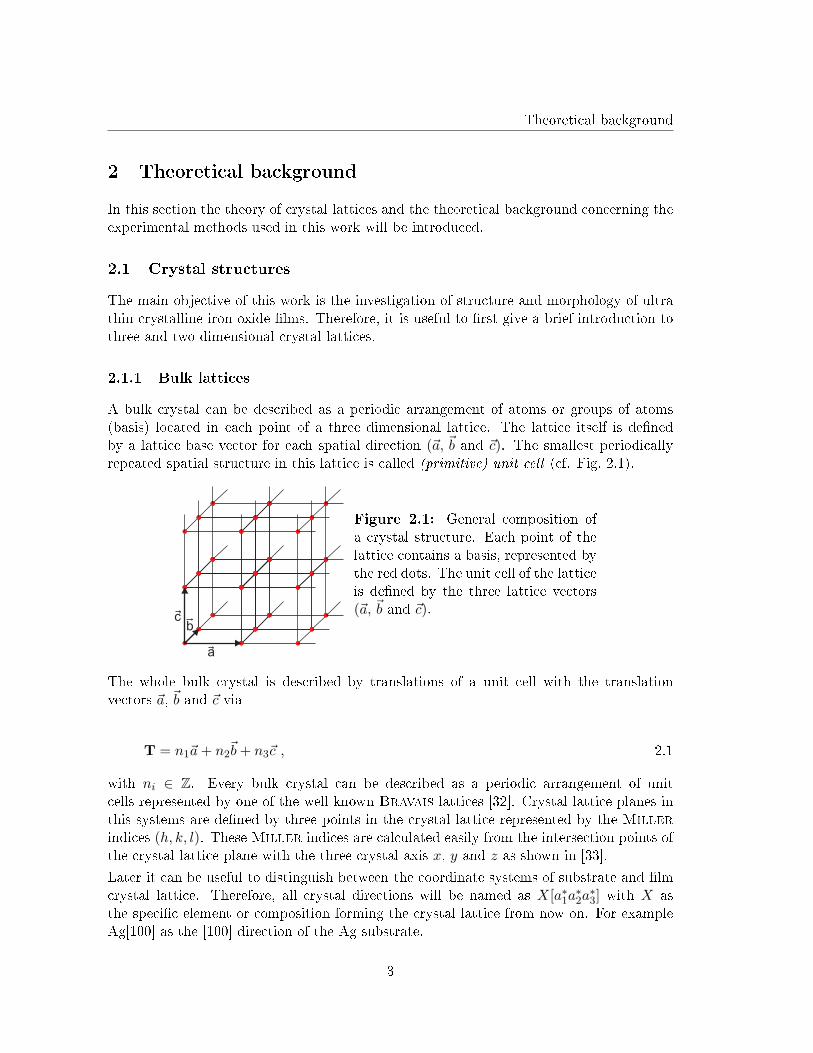
A bulk crystal can be described as a periodic arrangement of atoms or groups of atoms(basis) located in each point of a three dimensional lattice. The lattice itself is de�nedby a lattice base vector for each spatial direction (~a, ~b and ~c). The smallest periodicallyrepeated spatial structure in this lattice is called (primitive) unit cell (cf. Fig. 2.1).
a
bc
Figure 2.1: General composition ofa crystal structure. Each point of thelattice contains a basis, represented bythe red dots. The unit cell of the latticeis de�ned by the three lattice vectors(~a, ~b and ~c).
The whole bulk crystal is described by translations of a unit cell with the translationvectors ~a, ~b and ~c via
T = n1~a+ n2~b+ n3~c , 2.1
with ni ∈ Z. Every bulk crystal can be described as a periodic arrangement of unitcells represented by one of the well known Bravais lattices [32]. Crystal lattice planes inthis systems are de�ned by three points in the crystal lattice represented by the Millerindices (h, k, l). These Miller indices are calculated easily from the intersection points ofthe crystal lattice plane with the three crystal axis x, y and z as shown in [33].
Later it can be useful to distinguish between the coordinate systems of substrate and �lmcrystal lattice. Therefore, all crystal directions will be named as X[a∗1a
∗2a∗3] with X as
the speci�c element or composition forming the crystal lattice from now on. For exampleAg[100] as the [100] direction of the Ag substrate.
3
Theoretical background
2.1.2 Surface lattices
In�nite extended bulk crystals as introduced in section 2.1.1 do not exist in nature, sinceevery crystal has certain limiting planes and edges. The topmost atomic layers under-neath these limiting planes are called the crystal surface and can be described by a twodimensional lattice similar to Eq. 2.1 via
T = n1~a+ n2~b . 2.2
The crystal planes below the surface are called bulk. The crystals that are used to supportthin �lms are commonly called substrates. Hence, we will from now on use the phrasesubstrate lattice as a synonym for bulk lattice. The chemical surrounding at the surfacedi�ers from the surrounding inside the substrate because of missing binding partners. Thischange can lead to relaxations and reconstructions in the surface lattice if it is energeticallyfavorable. Reconstructions also occur through the adsorption of foreign atoms at thesurface. These adsorbate induced reconstructions are called superstructures. Therefore, itis necessary to describe the translation operations between the substrate lattice (given bythe set of base vectors (~a, ~b)) and the reconstructed surface lattice (de�ned by (~a′, ~b′)).
In general, there are two kinds of notations to describe the relation between surface latticeand substrate, namely the Wood's notation [34] and the matrix notation according toPark and Madden [35]. The Wood's notation can only be used if the surface andthe substrate lattice are commensurable, thus, the angle between the base vectors of bothlattices have to be the same. If that is the case theWood's notation describes the relationas
R(hkl)
(~a′
~a×~b′
~b
)/α , 2.3
while R represents the substrate material, (hkl) are theMiller indices of the crystal planeparallel to the surface and α is the rotation angle between the base of substrate and surfacelattice. For incommensurable surface and substrate lattices the matrix notation accordingto Park and Madden connects the sets of base vectors via
(~a′
~b′
)=
(m11 m12
m21 m22
)(~a~b
), 2.4
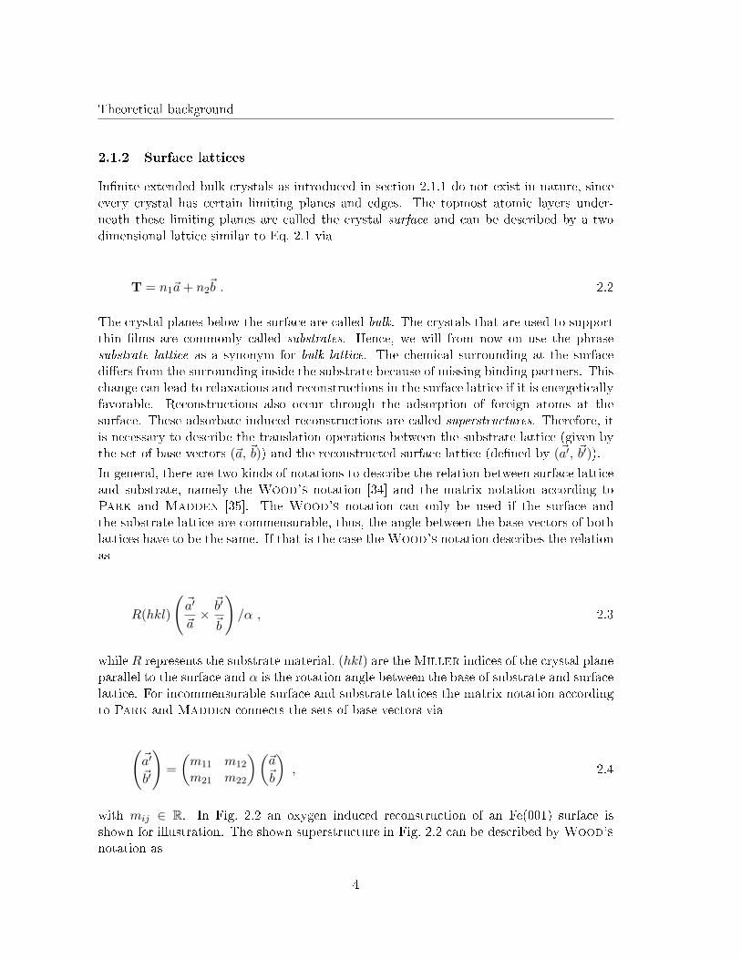
with mij ∈ R. In Fig. 2.2 an oxygen induced reconstruction of an Fe(001) surface isshown for illustration. The shown superstructure in Fig. 2.2 can be described by Wood's
notation as
4
Theoretical background
Fe[100]
Fe
[01
0]
Fe
Ob
a
b'
a'
Figure 2.2: Illustration of an oxygen induced superstructure on a Fe(001) surface.The base vectors of the unreconstructed surface are ~a and ~b, while the superstructureis de�ned by the base vectors ~a′ and ~b′ .
Fe(001)(2× 1) , 2.5
while matrix notation according to Park and Madden gives
(~a′
~b′
)=
(2 00 1
)(~a~b
). 2.6
2.1.3 Growth modes
The epitaxial growth of a thin crystalline �lm on a substrate is conditioned by the crystalstructures, lattice mis�t and the surface energies of �lm, substrate and interface. If thecrystal structure of �lm and substrate are the same and the surface energies are in thesame order of magnitude the growth of the �lm is dominated by the lattice mis�t η0 with
η0 = 2 · b0 − a0
b0 + a0. 2.7
Here a0 and b0 are the lattice constants of the substrate and the �lm, respectively [36].Large lattice mis�ts lead to strain, which is decreased by the formation of e.g. dislocations,mosaics and undulations (dislocation networks) as will be introduced later. This is not thecase if the lattice mis�t between �lm and substrate is very small or the system consists ofdi�erent crystal structures and di�erent types of bindings (e.g. ionic crystal/metal). Inthis case, the ratio between the surface free energies of �lm and substrate and the interfacefree energy governs the growth mode [36]. The growth of Fe on Ag(001) (lattice mis�t0.7%) and its oxides (FeOx/Ag(001) (ionic crystal/metal)), studied in this work, dependsstrongly on the di�erent surface free energies [37, 38, 39]. Hence, the di�erent growthmodes and their dependence on the surface free energies will be discussed in the following.
5
Theoretical background
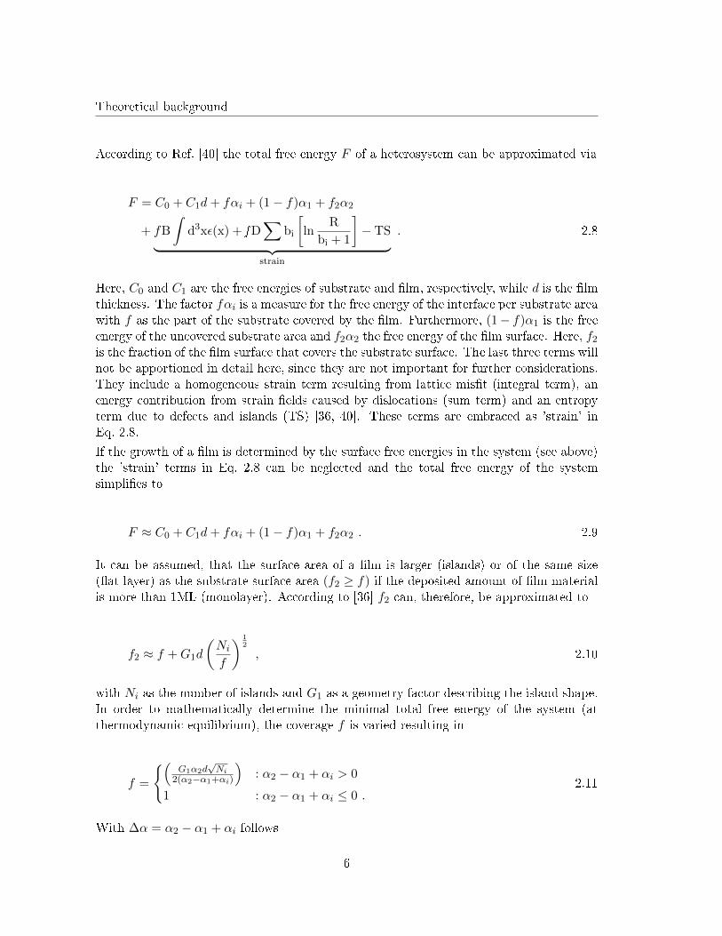
According to Ref. [40] the total free energy F of a heterosystem can be approximated via
F = C0 + C1d+ fαi + (1− f)α1 + f2α2
+ fB
∫d3xε(x) + fD
∑bi
[ln
R
bi + 1
]− TS︸ ︷︷ ︸
strain
. 2.8
Here, C0 and C1 are the free energies of substrate and �lm, respectively, while d is the �lmthickness. The factor fαi is a measure for the free energy of the interface per substrate areawith f as the part of the substrate covered by the �lm. Furthermore, (1− f)α1 is the freeenergy of the uncovered substrate area and f2α2 the free energy of the �lm surface. Here, f2
is the fraction of the �lm surface that covers the substrate surface. The last three terms willnot be apportioned in detail here, since they are not important for further considerations.They include a homogeneous strain term resulting from lattice mis�t (integral term), anenergy contribution from strain �elds caused by dislocations (sum term) and an entropyterm due to defects and islands (TS) [36, 40]. These terms are embraced as 'strain' inEq. 2.8.
If the growth of a �lm is determined by the surface free energies in the system (see above)the 'strain' terms in Eq. 2.8 can be neglected and the total free energy of the systemsimpli�es to
F ≈ C0 + C1d+ fαi + (1− f)α1 + f2α2 . 2.9
It can be assumed, that the surface area of a �lm is larger (islands) or of the same size(�at layer) as the substrate surface area (f2 ≥ f) if the deposited amount of �lm materialis more than 1ML (monolayer). According to [36] f2 can, therefore, be approximated to
f2 ≈ f +G1d
(Ni
f
) 12
, 2.10
with Ni as the number of islands and G1 as a geometry factor describing the island shape.In order to mathematically determine the minimal total free energy of the system (atthermodynamic equilibrium), the coverage f is varied resulting in
f =
{(G1α2d
√Ni
2(α2−α1+αi)
): α2 − α1 + αi > 0
1 : α2 − α1 + αi ≤ 0 .2.11
With ∆α = α2 − α1 + αi follows
6
Theoretical background
∆α ≤ 0 ⇒ Frank-van-der-Merve growth (layer− by − layer) and 2.12
∆α > 0 ⇒ Volmer-Weber growth (islands) . 2.13
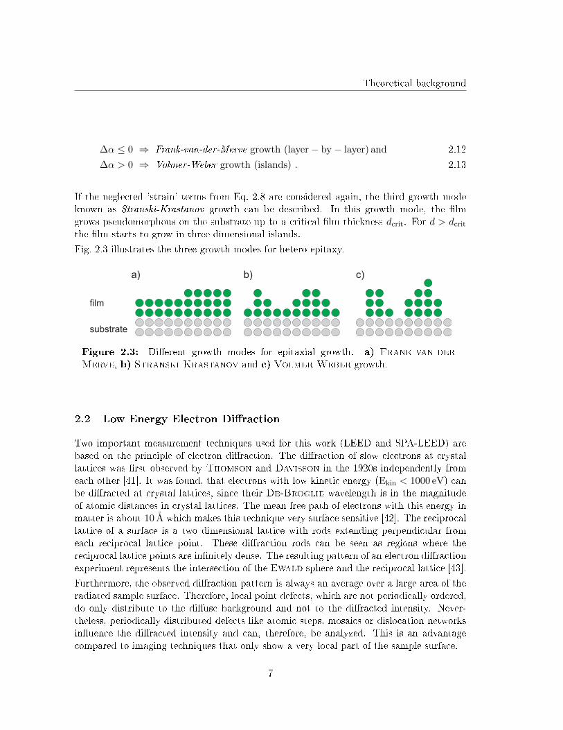
If the neglected 'strain' terms from Eq. 2.8 are considered again, the third growth modeknown as Stranski-Krastanov growth can be described. In this growth mode, the �lmgrows pseudomorphous on the substrate up to a critical �lm thickness dcrit. For d > dcrit
the �lm starts to grow in three dimensional islands.
Fig. 2.3 illustrates the three growth modes for hetero-epitaxy.
a) b) c)
substrate
film
Figure 2.3: Di�erent growth modes for epitaxial growth. a) Frank-van-der-
Merve, b) Stranski-Krastanov and c) Volmer-Weber growth.
2.2 Low Energy Electron Di�raction
Two important measurement techniques used for this work (LEED and SPA-LEED) arebased on the principle of electron di�raction. The di�raction of slow electrons at crystallattices was �rst observed by Thomson and Davisson in the 1920s independently fromeach other [41]. It was found, that electrons with low kinetic energy (Ekin < 1000 eV) canbe di�racted at crystal lattices, since their De-Broglie wavelength is in the magnitudeof atomic distances in crystal lattices. The mean free path of electrons with this energy inmatter is about 10 A which makes this technique very surface sensitive [42]. The reciprocallattice of a surface is a two dimensional lattice with rods extending perpendicular fromeach reciprocal lattice point. These di�raction rods can be seen as regions where thereciprocal lattice points are in�nitely dense. The resulting pattern of an electron di�ractionexperiment represents the intersection of the Ewald sphere and the reciprocal lattice [43].
Furthermore, the observed di�raction pattern is always an average over a large area of theradiated sample surface. Therefore, local point defects, which are not periodically ordered,do only distribute to the di�use background and not to the di�racted intensity. Never-theless, periodically distributed defects like atomic steps, mosaics or dislocation networksin�uence the di�racted intensity and can, therefore, be analyzed. This is an advantagecompared to imaging techniques that only show a very local part of the sample surface.
7
Theoretical background
2.2.1 Kinematic theory of electron di�raction
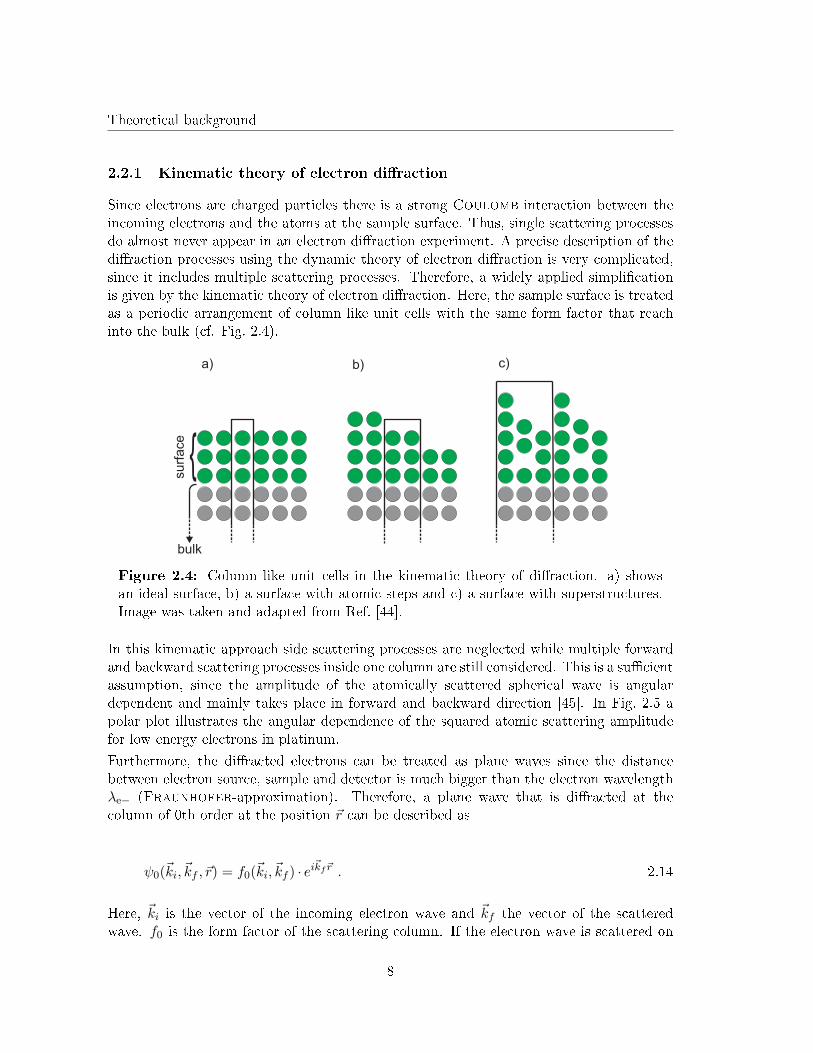
Since electrons are charged particles there is a strong Coulomb interaction between theincoming electrons and the atoms at the sample surface. Thus, single scattering processesdo almost never appear in an electron di�raction experiment. A precise description of thedi�raction processes using the dynamic theory of electron di�raction is very complicated,since it includes multiple scattering processes. Therefore, a widely applied simpli�cationis given by the kinematic theory of electron di�raction. Here, the sample surface is treatedas a periodic arrangement of column like unit cells with the same form factor that reachinto the bulk (cf. Fig. 2.4).
{
surf
ace
bulk
a) b) c)
Figure 2.4: Column like unit cells in the kinematic theory of di�raction. a) showsan ideal surface, b) a surface with atomic steps and c) a surface with superstructures.Image was taken and adapted from Ref. [44].
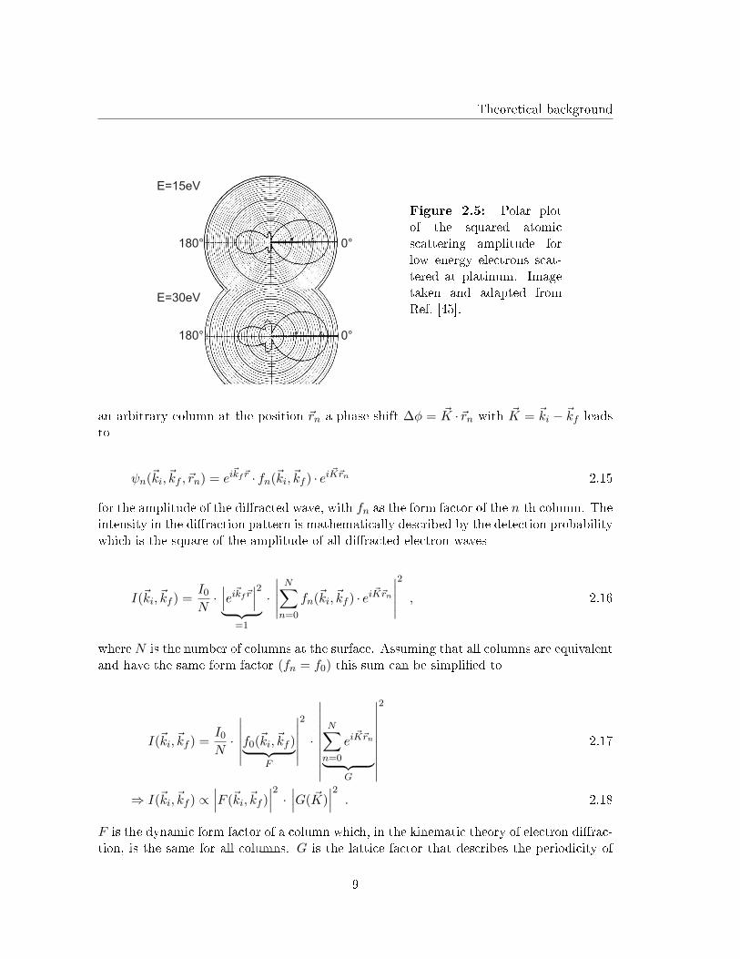
In this kinematic approach side scattering processes are neglected while multiple forwardand backward scattering processes inside one column are still considered. This is a su�cientassumption, since the amplitude of the atomically scattered spherical wave is angulardependent and mainly takes place in forward and backward direction [45]. In Fig. 2.5 apolar plot illustrates the angular dependence of the squared atomic scattering amplitudefor low energy electrons in platinum.
Furthermore, the di�racted electrons can be treated as plane waves since the distancebetween electron source, sample and detector is much bigger than the electron wavelengthλe− (Fraunhofer-approximation). Therefore, a plane wave that is di�racted at thecolumn of 0th order at the position ~r can be described as
ψ0(~ki,~kf , ~r) = f0(~ki,~kf ) · ei~kf~r . 2.14
Here, ~ki is the vector of the incoming electron wave and ~kf the vector of the scatteredwave. f0 is the form factor of the scattering column. If the electron wave is scattered on
8
Theoretical background
E=15eV
E=30eV
180°
180°
0°
0°
Figure 2.5: Polar plotof the squared atomicscattering amplitude forlow energy electrons scat-tered at platinum. Imagetaken and adapted fromRef. [45].
an arbitrary column at the position ~rn a phase shift ∆φ = ~K ·~rn with ~K = ~ki − ~kf leadsto
ψn(~ki,~kf , ~rn) = ei~kf~r · fn(~ki,~kf ) · ei ~K~rn 2.15
for the amplitude of the di�racted wave, with fn as the form factor of the n-th column. Theintensity in the di�raction pattern is mathematically described by the detection probabilitywhich is the square of the amplitude of all di�racted electron waves
I(~ki,~kf ) =I0
N·∣∣∣ei~kf~r∣∣∣2︸ ︷︷ ︸
=1
·
∣∣∣∣∣N∑n=0
fn(~ki,~kf ) · ei ~K~rn∣∣∣∣∣2
, 2.16
where N is the number of columns at the surface. Assuming that all columns are equivalentand have the same form factor (fn = f0) this sum can be simpli�ed to
I(~ki,~kf ) =I0
N·
∣∣∣∣∣∣f0(~ki,~kf )︸ ︷︷ ︸F
∣∣∣∣∣∣2
·
∣∣∣∣∣∣∣∣∣∣N∑n=0
ei~K~rn
︸ ︷︷ ︸G
∣∣∣∣∣∣∣∣∣∣
2
2.17
⇒ I(~ki,~kf ) ∝∣∣∣F (~ki,~kf )
∣∣∣2 · ∣∣∣G( ~K)∣∣∣2 . 2.18
F is the dynamic form factor of a column which, in the kinematic theory of electron di�rac-tion, is the same for all columns. G is the lattice factor that describes the periodicity of
9
Theoretical background
the columns and contains information about position and shape of the di�racted intensity.Therefore, the lattice factor G can be used to investigate the crystal structure and mor-phology of the sample surface. The dynamic form factor F describes the absolute intensityof the di�racted intensity peaks in the di�raction pattern. It also contains multiple scat-tering processes and is, therefore, not exactly described in the kinematic theory of electrondi�raction. Hence, in the following we will concentrate on the description of the latticefactor G( ~K), which can be written as
∣∣∣G( ~K)∣∣∣2 = G( ~K)G( ~K)∗ =
∑n
∑m
ei~K~rne−i
~K~rm =∑n,m
ei~K(~rn−~rm) , 2.19
where the scattering centers are located at the crystal lattice positions
~rn = n1~a+ n2~b+ (n1, n2)~d , 2.20
with n1, n2 ∈ Z [46]. Here, ~a and ~b are the surface lattice vectors and ~d is the vectorperpendicular to the surface with the length of the layer distance. Assuming an idealsurface with no height di�erences between the unit cells (no steps) the position of thescattering centers simpli�es to
~rn,ideal = n1~a+ n2~b . 2.21
Additionally, the scattering vector ~K can be separated into its parts perpendicular andparallel to the surface via ~K = ~k⊥ + ~k‖. For an ideal surface without any steps ~k⊥ isarbitrary in the Laue conditions for constructive interference [33]. Thus, the scatteringvector reduces to its parallel component ~K = ~k‖ and Eq. 2.19 can be transformed into
∣∣∣G( ~K)∣∣∣2ideal
=∑n
ei~k‖~rn,ideal =
∑n1,n2
ei~k‖(n1~a+n2
~b) . 2.22
It is known from Laue theory [33] that the direct product of the primitive base vectors ofreciprocal and real space is given by the Laue equations
~a ·~k‖ = 2πh and 2.23
~b ·~k‖ = 2πk , 2.24
with h and k as the Miller indices.
Therefore, Eq. 2.22 results in
∣∣∣G( ~K)∣∣∣2ideal
=∑n1,n2
e2πi(n1h+n2k) . 2.25
Since n1, n2, h, k ∈ Z, this is a delta distribution of the di�racted intensity. This deltadistribution represents the expected di�raction pattern from an ideal surface.
10
Theoretical background
2.2.2 Atomically stepped surfaces
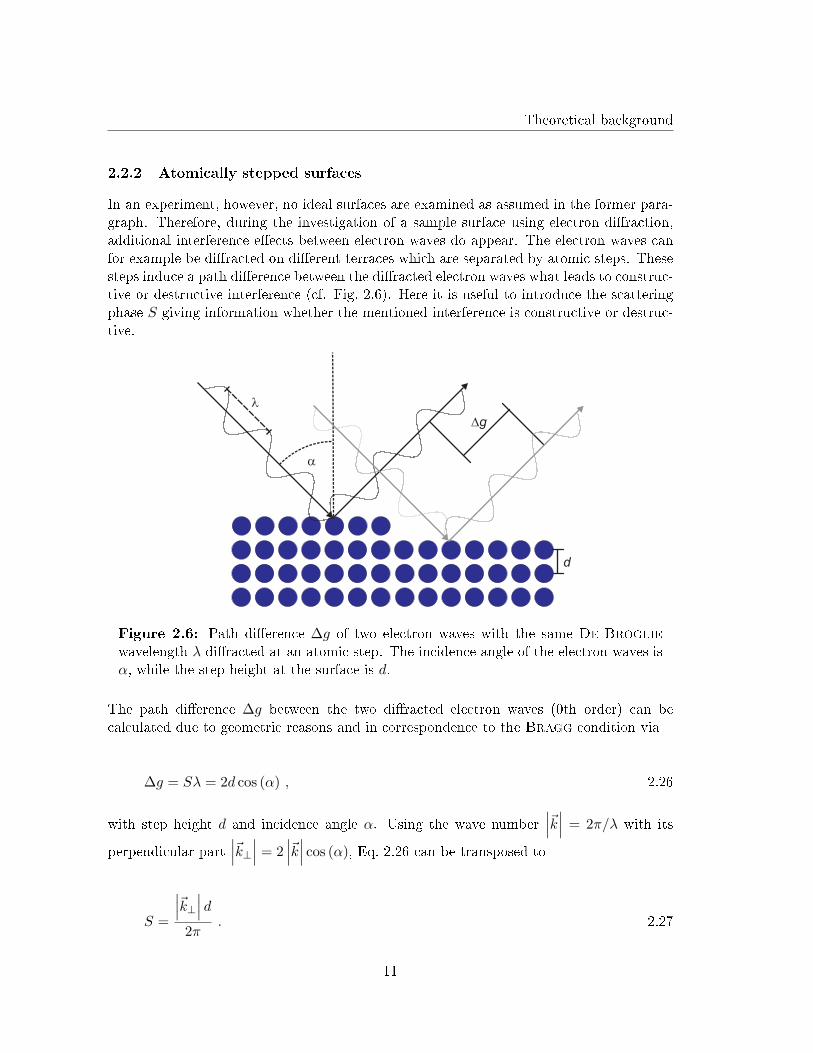
In an experiment, however, no ideal surfaces are examined as assumed in the former para-graph. Therefore, during the investigation of a sample surface using electron di�raction,additional interference e�ects between electron waves do appear. The electron waves canfor example be di�racted on di�erent terraces which are separated by atomic steps. Thesesteps induce a path di�erence between the di�racted electron waves what leads to construc-tive or destructive interference (cf. Fig. 2.6). Here it is useful to introduce the scatteringphase S giving information whether the mentioned interference is constructive or destruc-tive.
d
Dg
a
l
Figure 2.6: Path di�erence ∆g of two electron waves with the same De-Brogliewavelength λ di�racted at an atomic step. The incidence angle of the electron waves isα, while the step height at the surface is d.
The path di�erence ∆g between the two di�racted electron waves (0th order) can becalculated due to geometric reasons and in correspondence to the Bragg condition via
∆g = Sλ = 2d cos (α) , 2.26
with step height d and incidence angle α. Using the wave number∣∣∣~k∣∣∣ = 2π/λ with its
perpendicular part∣∣∣~k⊥∣∣∣ = 2
∣∣∣~k∣∣∣ cos (α), Eq. 2.26 can be transposed to
S =
∣∣∣~k⊥∣∣∣ d2π
. 2.27
11
Theoretical background
In accordance to the Bragg condition (cf. Eq. 2.26) constructive interference occurs if Sis an integral number (in-phase), while for half integral S the interference is destructive(out-of-phase). From an experimental point of view it is useful to describe the relationbetween the scattering phase S and the electron energy, since this is the important tunableparameter in an electron di�raction experiment. Therefore, the De-Broglie wavelengthλ = 2π~/
√2meE is inserted into Eq. 2.26 which results in
S =d cos (α)
√2meE
π~. 2.28
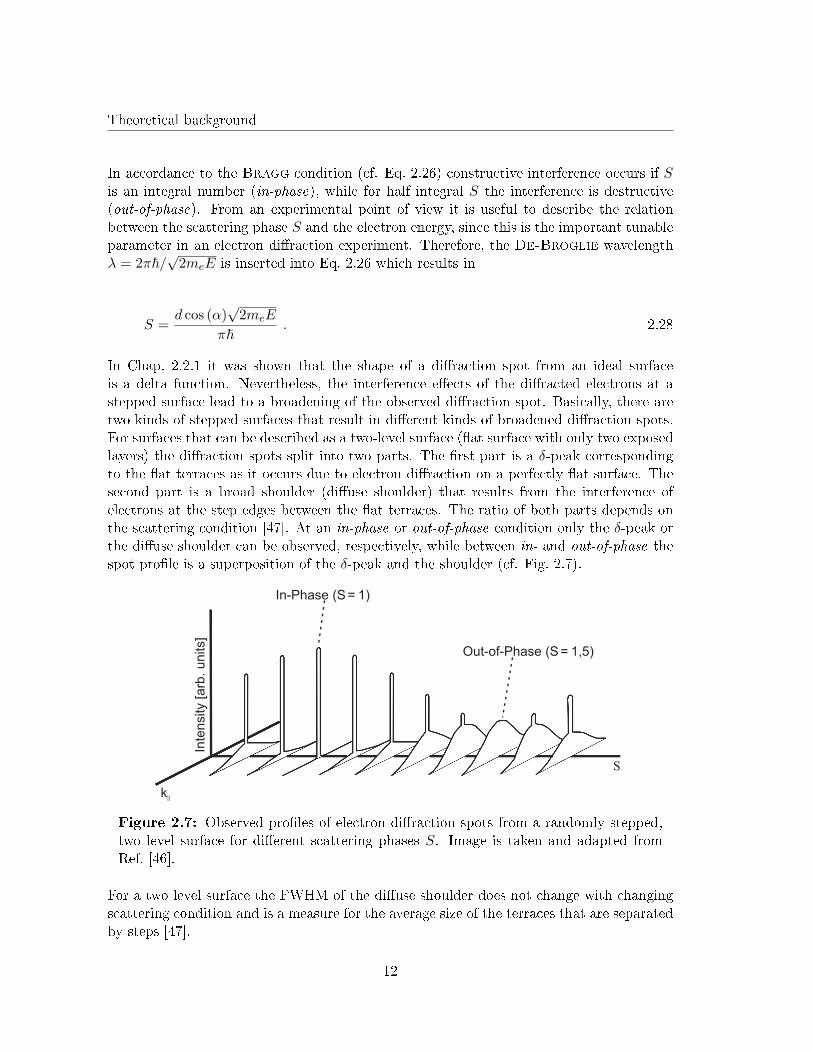
In Chap. 2.2.1 it was shown that the shape of a di�raction spot from an ideal surfaceis a delta function. Nevertheless, the interference e�ects of the di�racted electrons at astepped surface lead to a broadening of the observed di�raction spot. Basically, there aretwo kinds of stepped surfaces that result in di�erent kinds of broadened di�raction spots.For surfaces that can be described as a two-level surface (�at surface with only two exposedlayers) the di�raction spots split into two parts. The �rst part is a δ-peak correspondingto the �at terraces as it occurs due to electron di�raction on a perfectly �at surface. Thesecond part is a broad shoulder (di�use shoulder) that results from the interference ofelectrons at the step edges between the �at terraces. The ratio of both parts depends onthe scattering condition [47]. At an in-phase or out-of-phase condition only the δ-peak orthe di�use shoulder can be observed, respectively, while between in- and out-of-phase thespot pro�le is a superposition of the δ-peak and the shoulder (cf. Fig. 2.7).
k||
Inte
nsity [arb
. units]
In-Phase (S = 1)
Out-of-Phase (S= 1,5)
S
Figure 2.7: Observed pro�les of electron di�raction spots from a randomly stepped,two level surface for di�erent scattering phases S. Image is taken and adapted fromRef. [46].
For a two level surface the FWHM of the di�use shoulder does not change with changingscattering condition and is a measure for the average size of the terraces that are separatedby steps [47].
12
Theoretical background
A rough surface which can not be described by a �nite number of layers is called multilevelsurface. The di�raction spots obtained from a multilevel surface can not be separated intotwo parts. The FWHM of these di�raction spots varies periodically with the scatteringphase while the peak form at an in-phase condition is still δ-shaped [47].
2.2.3 H(S) analysis
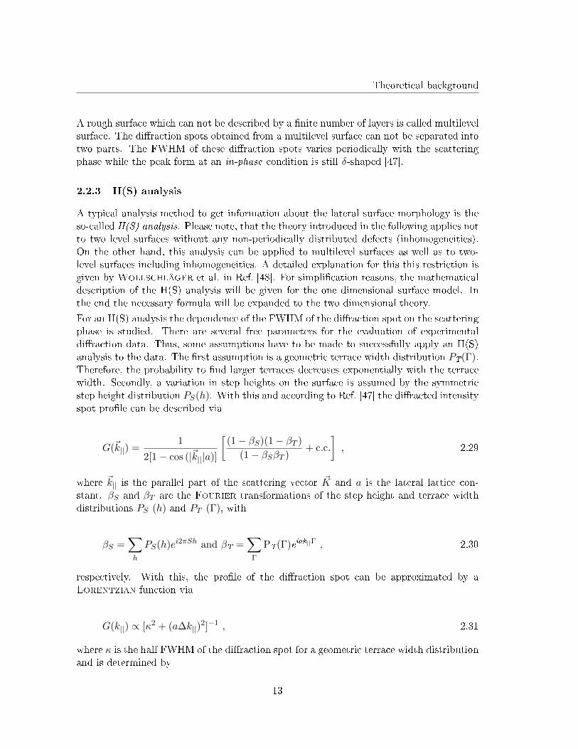
A typical analysis method to get information about the lateral surface morphology is theso-called H(S) analysis. Please note, that the theory introduced in the following applies notto two level surfaces without any non-periodically distributed defects (inhomogeneities).On the other hand, this analysis can be applied to multilevel surfaces as well as to two-level surfaces including inhomogeneities. A detailed explanation for this this restriction isgiven by Wollschläger et al. in Ref. [48]. For simpli�cation reasons, the mathematicaldescription of the H(S) analysis will be given for the one dimensional surface model. Inthe end the necessary formula will be expanded to the two dimensional theory.
For an H(S) analysis the dependence of the FWHM of the di�raction spot on the scatteringphase is studied. There are several free parameters for the evaluation of experimentaldi�raction data. Thus, some assumptions have to be made to successfully apply an H(S)analysis to the data. The �rst assumption is a geometric terrace width distribution PT(Γ).Therefore, the probability to �nd larger terraces decreases exponentially with the terracewidth. Secondly, a variation in step heights on the surface is assumed by the symmetricstep height distribution PS(h). With this and according to Ref. [47] the di�racted intensityspot pro�le can be described via
G(~k||) =1
2[1− cos (|~k|||a)]
[(1− βS)(1− βT )
(1− βSβT )+ c.c.
], 2.29
where ~k|| is the parallel part of the scattering vector ~K and a is the lateral lattice con-stant. βS and βT are the Fourier transformations of the step height and terrace widthdistributions PS (h) and PT (Γ), with
βS =∑h
PS(h)ei2πSh and βT =∑
Γ
PT(Γ)eiak||Γ , 2.30
respectively. With this, the pro�le of the di�raction spot can be approximated by aLorentzian function via
G(k||) ∝ [κ2 + (a∆k||)2]−1 , 2.31
where κ is the half FWHM of the di�raction spot for a geometric terrace width distributionand is determined by
13
Theoretical background
2κ = a∆k|| =2(1− βS(S))
〈Γ〉, 2.32
as shown in Ref. [46]. For single atomic steps with uniform height (h ∈ {1,−1} →PS(h) = 1
2) follows from Eq. 2.30
βS(S) =1
2ei2πS +
1
2e−i2πS = cos(2πS) , 2.33
and, therefore, the FWHM of the spot pro�le results in
a∆k|| =2(1− cos(2πS))
〈Γ〉. 2.34
It is useful to convert the FWHM of the di�raction spots into units of [%BZ], since ex-perimental data usually gives disctances between di�raction spots in percentage of theBrillouin-zone. The spot pro�les FWHM (∆k||) expressed in units of [%BZ] is
∆k|| =a∆k||
2π· 100%BZ 2.35
=κ
π· 100%BZ =
100%BZ(1− cos(2πS))
〈Γ〉π. 2.36
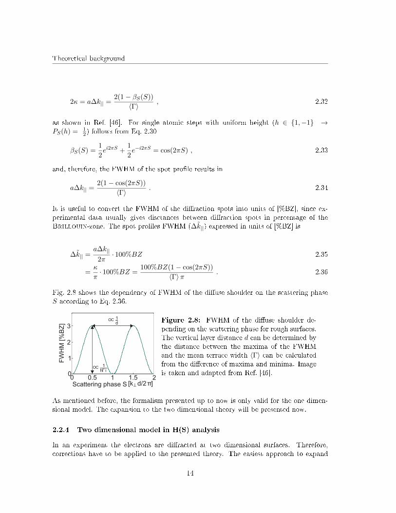
Fig. 2.8 shows the dependency of FWHM of the di�use shoulder on the scattering phaseS according to Eq. 2.36.
FW
HM
[%
BZ
]
Scattering phase S0 0.5 1 1.5 2
1
2
3
0
[k⊥d/2π]
∝1d
∝1
hΓ i
Figure 2.8: FWHM of the di�use shoulder de-pending on the scattering phase for rough surfaces.The vertical layer distance d can be determined bythe distance between the maxima of the FWHMand the mean terrace width 〈Γ〉 can be calculatedfrom the di�erence of maxima and minima. Imageis taken and adapted from Ref. [46].
As mentioned before, the formalism presented up to now is only valid for the one dimen-sional model. The expansion to the two dimensional theory will be presented now.
2.2.4 Two dimensional model in H(S) analysis
In an experiment the electrons are di�racted at two dimensional surfaces. Therefore,corrections have to be applied to the presented theory. The easiest approach to expand
14
Theoretical background
the one dimensional to a two dimensional theory is the replacement of the Lorentzianfunction approximating the lattice factor G( ~K) by a modi�ed Lorentzian which will bedescribed now very brie�y. Since the mathematical derivation goes beyond the scope of thiswork, please see Ref. [47] for details. In general, the shape of the function describing thelattice factor G( ~K) is determined by the pair correlation function C(~r). Having a scatteringcenter at the position ~r = 0, this pair correlation function describes the probability to �nda second scattering center at a given position ~r 6= 0. If the pair correlation function is thesame for every direction (isotropic), this leads to a modi�ed Lorentzian function
G( ~k||) ∝ [1 + ( ~k||/κ)2]−32 2.37
approximating G( ~k||) at a two dimensional surface [47]. The mentioned assumption of anisotropic pair correlation function can be proved in the experiment by the symmetry of thedi�raction spots. From this correction of the Lorentzian function follows a∆k|| 6= 2κ.
Thus, the modi�cation of the spot pro�le approximation function (Lor→Lor32 ) leads to a
correction term in Eq. 2.36 giving
∆k||,2D =
√2
1α − 1
[100%BZ(1− cos(2πS))
〈Γ〉π
]2.38
=
√2
23 − 1
[100%BZ(1− cos(2πS))
〈Γ〉π
], 2.39
with α = 3/2 as the modi�cation factor originating from (Lor→Lor32 ).
2.2.5 Mosaics and facets
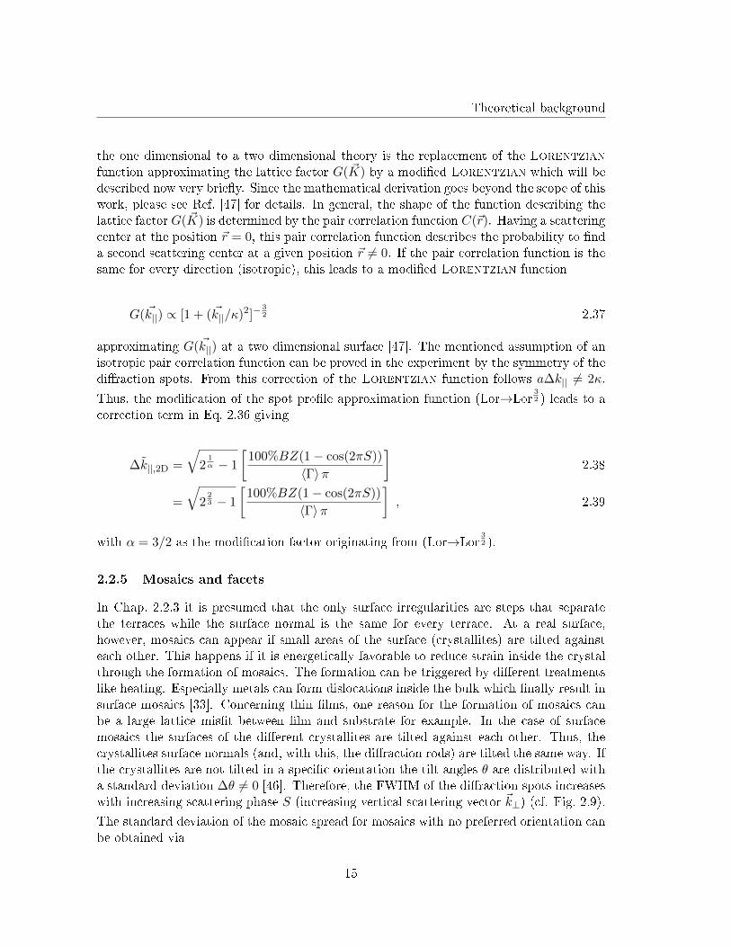
In Chap. 2.2.3 it is presumed that the only surface irregularities are steps that separatethe terraces while the surface normal is the same for every terrace. At a real surface,however, mosaics can appear if small areas of the surface (crystallites) are tilted againsteach other. This happens if it is energetically favorable to reduce strain inside the crystalthrough the formation of mosaics. The formation can be triggered by di�erent treatmentslike heating. Especially metals can form dislocations inside the bulk which �nally result insurface mosaics [33]. Concerning thin �lms, one reason for the formation of mosaics canbe a large lattice mis�t between �lm and substrate for example. In the case of surfacemosaics the surfaces of the di�erent crystallites are tilted against each other. Thus, thecrystallites surface normals (and, with this, the di�raction rods) are tilted the same way. Ifthe crystallites are not tilted in a speci�c orientation the tilt angles θ are distributed witha standard deviation ∆θ 6= 0 [46]. Therefore, the FWHM of the di�raction spots increaseswith increasing scattering phase S (increasing vertical scattering vector ~k⊥) (cf. Fig. 2.9).
The standard deviation of the mosaic spread for mosaics with no preferred orientation canbe obtained via
15
Theoretical background
(00) (01)(0 )1 (01)(0 )1 ∆ k||
k⊥
k⊥
k||k||
a) b)
Figure 2.9: a) Di�raction rods from an ideal surface. b) Di�raction rods from asurface with mosaics without preferred direction. The FWHM increases linear with thescattering vector ~k⊥. Image is taken from Ref. [46] and modi�ed.
∆k||
2 · k⊥= tan
(∆θ
2
)≈ ∆θ
2, 2.40
for small angles θ. Together with Eq. 2.36 and 2.27 the standard deviation of the mosaicspread results in
∆θ
2≈
d ·∆k||a · 200%BZ ·S
, 2.41
where d denotes the step height and a the lateral lattice constant of the investigatedsurface. The linear increase of FWHM of the di�raction spots due to such mosaics alsoa�ects the prior shown H(S) analysis (Chap. 2.2.3). A linear term is added to Eq. 2.36(one dimensional theory) in order to incorporate the mosaic spread by
∆k||,mosaic =
[100%BZ(1− cos(2πS))
〈Γ〉π+a
d∆θ ·S
]. 2.42
Expansion to the two dimensional theory (cf. Eq. 2.39) results in
∆k||,mosaic,2D =
√2
23 − 1
[100%BZ(1− cos(2πS))
〈Γ〉π+a
d∆θ ·S
]. 2.43
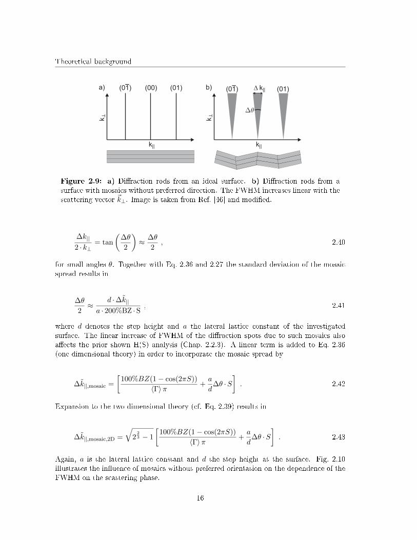
Again, a is the lateral lattice constant and d the step height at the surface. Fig. 2.10illustrates the in�uence of mosaics without preferred orientation on the dependence of theFWHM on the scattering phase.
16
Theoretical backgroundF
WH
M [%
BZ
]
Scattering phase S0 0.5 1 1.5 2
1
2
3
0
[k⊥d/2 π]
∝∆Θ
Figure 2.10: FWHM of the di�use shoulder de-pending on the scattering phase for rough surfaceswith mosaics without preferred orientation. Themosaic spread ∆θ can be determined by the in-clination angle of the curve. Image is taken andadapted from Ref. [46].
Other structural features at the surface that in�uence the di�raction experiments are facets.Even though facets were not detected at any surface during this work, it is useful to knowhow facets in�uence the di�raction pattern for later discussion of some experimental results.In contrast to mosaics, facets are no tilted crystallites but consist of short terraces of thesame length, while the surface normal of each terrace is still the same as for the idealsubstrate. Only the average orientation angle of the whole facet is not zero. In contrast tomosaics with no preferred orientation a facet exhibits a speci�c average orientation angle.This orientation angle corresponds to a speci�c crystal plane that can be characterized bythe Miller indices (hkl). A visualization of facets formed at a (001) surface is given inFig. 2.11.
(001) (001)
(001)
(011
) (01)
1
(00) (01)(0 )1
S=1
S=2
S=1.5
S=0.5
a)
b)
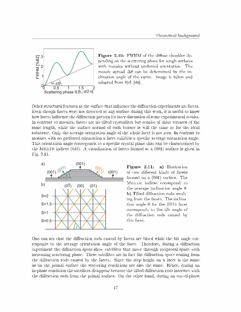
Figure 2.11: a) Illustrationof two di�erent kinds of facetsformed on a (001) surface. TheMiller indices correspond tothe average inclination angle θ.b) Tilted di�raction rods result-ing from the facets. The inclina-tion angle θ for the (011) facetcorresponds to the tilt angle ofthe di�raction rods caused bythis facet.
One can see that the di�raction rods caused by facets are tilted while the tilt angle cor-responds to the average orientation angle of the facet. Therefore, during a di�ractionexperiment the di�raction spots show satellites that move through reciprocal space withincreasing scattering phase. These satellites are in fact the di�raction spots coming fromthe di�raction rods caused by the facets. Since the step height on a facet is the sameas on the primal surface the scattering conditions are also the same. Hence, during anin-phase condition the satellites disappear because the tilted di�raction rods intersect withthe di�raction rods from the primal surface. On the other hand, during an out-of-phase
17
Theoretical background
condition the satellites (due to one facet) are equally separated from the central spot (cf.Fig. 2.11). Fig. 2.12 shows three examples of typical spot pro�les obtained at di�erentscattering conditions from a surface with facets.
S=1
S=1.25
S=1.5
(00)
k||
Figure 2.12: Typical di�raction spot pro-�les obtained from a (001) surface with onekind of facet (no counter facet) and remain-ing (001) terraces (central spot). The tilteddi�raction rods result in spots that changetheir position in reciprocal space (k⊥) withincreasing scattering phase S. These movingdi�raction spots are called satellites.
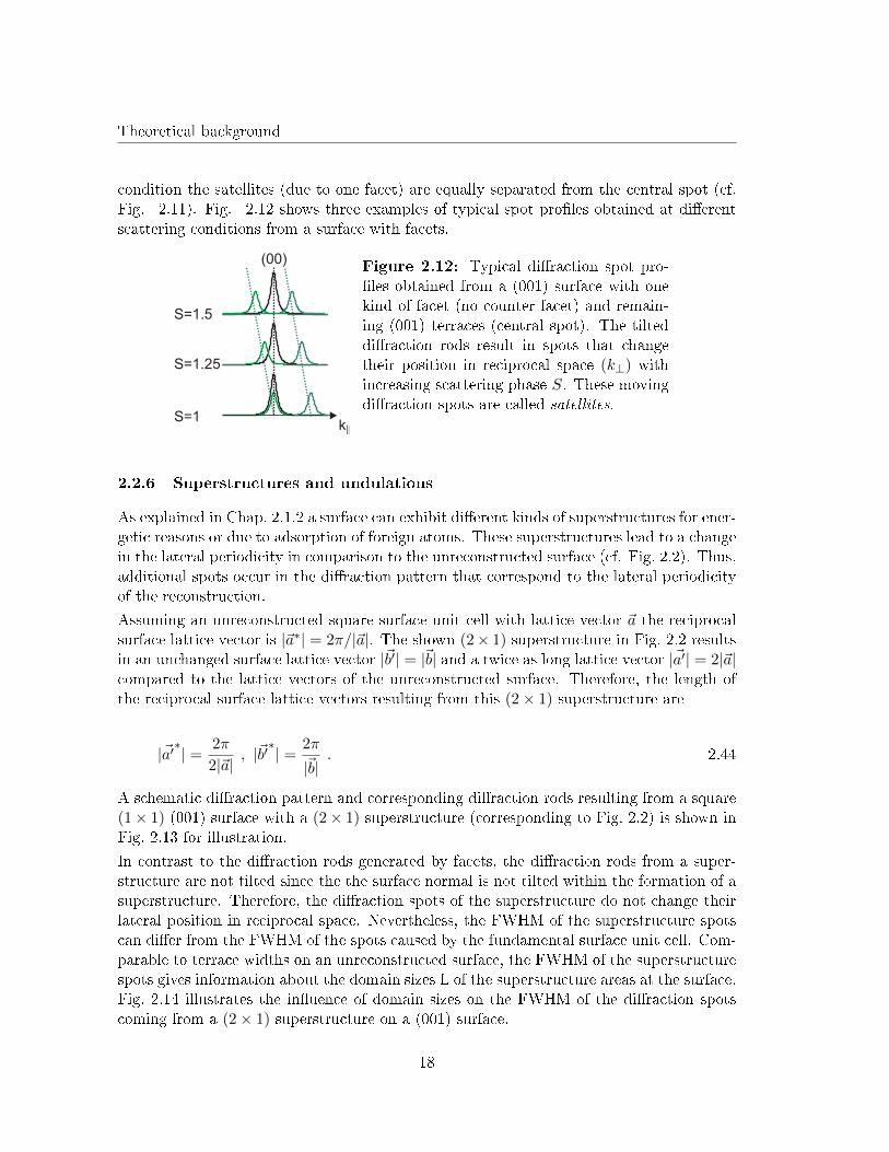
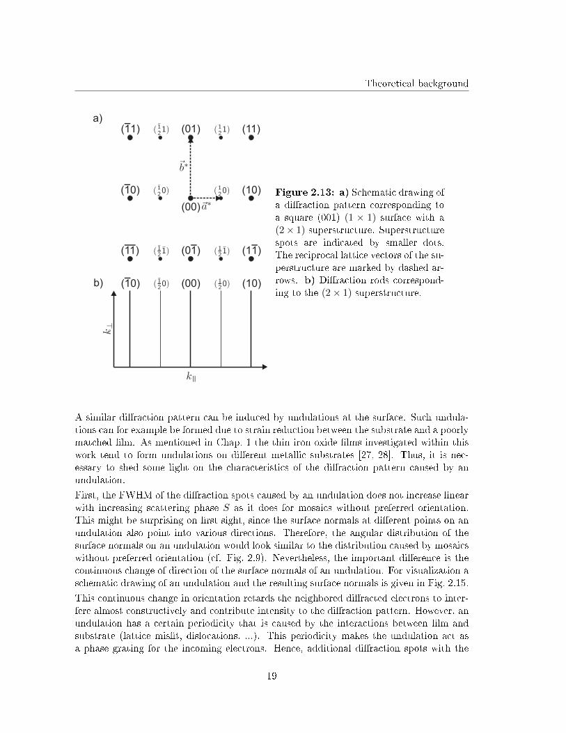
2.2.6 Superstructures and undulations
As explained in Chap. 2.1.2 a surface can exhibit di�erent kinds of superstructures for ener-getic reasons or due to adsorption of foreign atoms. These superstructures lead to a changein the lateral periodicity in comparison to the unreconstructed surface (cf. Fig. 2.2). Thus,additional spots occur in the di�raction pattern that correspond to the lateral periodicityof the reconstruction.
Assuming an unreconstructed square surface unit cell with lattice vector ~a the reciprocalsurface lattice vector is |~a∗| = 2π/|~a|. The shown (2× 1) superstructure in Fig. 2.2 resultsin an unchanged surface lattice vector |~b′| = |~b| and a twice as long lattice vector |~a′| = 2|~a|compared to the lattice vectors of the unreconstructed surface. Therefore, the length ofthe reciprocal surface lattice vectors resulting from this (2× 1) superstructure are
|~a′∗| = 2π
2|~a|, |~b′
∗| = 2π
|~b|. 2.44
A schematic di�raction pattern and corresponding di�raction rods resulting from a square(1× 1) (001) surface with a (2× 1) superstructure (corresponding to Fig. 2.2) is shown inFig. 2.13 for illustration.
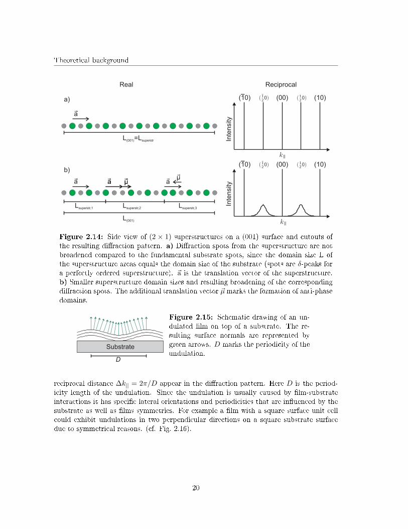
In contrast to the di�raction rods generated by facets, the di�raction rods from a super-structure are not tilted since the the surface normal is not tilted within the formation of asuperstructure. Therefore, the di�raction spots of the superstructure do not change theirlateral position in reciprocal space. Nevertheless, the FWHM of the superstructure spotscan di�er from the FWHM of the spots caused by the fundamental surface unit cell. Com-parable to terrace widths on an unreconstructed surface, the FWHM of the superstructurespots gives information about the domain sizes L of the superstructure areas at the surface.Fig. 2.14 illustrates the in�uence of domain sizes on the FWHM of the di�raction spotscoming from a (2× 1) superstructure on a (001) surface.
18
Theoretical background
(00)
(10)( 0)1
(01) (11)( 1)1
(0 )1 (1 )1( )11
(10)( 0)1 (00)b)
a)
||
Figure 2.13: a) Schematic drawing ofa di�raction pattern corresponding toa square (001) (1 × 1) surface with a(2× 1) superstructure. Superstructurespots are indicated by smaller dots.The reciprocal lattice vectors of the su-perstructure are marked by dashed ar-rows. b) Di�raction rods correspond-ing to the (2× 1) superstructure.
A similar di�raction pattern can be induced by undulations at the surface. Such undula-tions can for example be formed due to strain reduction between the substrate and a poorlymatched �lm. As mentioned in Chap. 1 the thin iron oxide �lms investigated within thiswork tend to form undulations on di�erent metallic substrates [27, 28]. Thus, it is nec-essary to shed some light on the characteristics of the di�raction pattern caused by anundulation.
First, the FWHM of the di�raction spots caused by an undulation does not increase linearwith increasing scattering phase S as it does for mosaics without preferred orientation.This might be surprising on �rst sight, since the surface normals at di�erent points on anundulation also point into various directions. Therefore, the angular distribution of thesurface normals on an undulation would look similar to the distribution caused by mosaicswithout preferred orientation (cf. Fig. 2.9). Nevertheless, the important di�erence is thecontinuous change of direction of the surface normals of an undulation. For visualization aschematic drawing of an undulation and the resulting surface normals is given in Fig. 2.15.
This continuous change in orientation retards the neighbored di�racted electrons to inter-fere almost constructively and contribute intensity to the di�raction pattern. However, anundulation has a certain periodicity that is caused by the interactions between �lm andsubstrate (lattice mis�t, dislocations, ...). This periodicity makes the undulation act asa phase grating for the incoming electrons. Hence, additional di�raction spots with the
19
Theoretical background
||
||
Real Reciprocal
(10)( 0)1 (00)
a
(10)( 0)1 (00)
a
a
µa µ aµ
L =L(001) superstr
L(001)
Lsuperstr,2Lsuperstr,1 Lsuperstr,3
a)
b)
Inte
nsity
Inte
nsity
Figure 2.14: Side view of (2 × 1) superstructures on a (001) surface and cutouts ofthe resulting di�raction pattern. a) Di�raction spots from the superstructure are notbroadened compared to the fundamental substrate spots, since the domain size L ofthe superstructure areas equals the domain size of the substrate (spots are δ-peaks fora perfectly ordered superstructure). ~a is the translation vector of the superstructure.b) Smaller superstructure domain sizes and resulting broadening of the correspondingdi�raction spots. The additional translation vector ~µ marks the formation of anti-phasedomains.
Substrate
D
Figure 2.15: Schematic drawing of an un-dulated �lm on top of a substrate. The re-sulting surface normals are represented bygreen arrows. D marks the periodicity of theundulation.
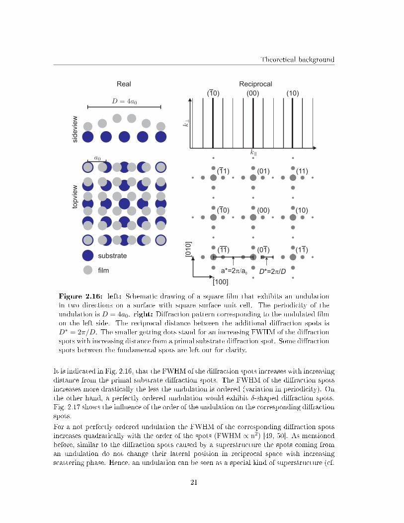
reciprocal distance ∆k|| = 2π/D appear in the di�raction pattern. Here D is the period-icity length of the undulation. Since the undulation is usually caused by �lm-substrateinteractions it has speci�c lateral orientations and periodicities that are in�uenced by thesubstrate as well as �lms symmetries. For example a �lm with a square surface unit cellcould exhibit undulations in two perpendicular directions on a square substrate surfacedue to symmetrical reasons. (cf. Fig. 2.16).
20
Theoretical background
||
substrate
film
top
vie
wsid
evie
w
Real Reciprocal
(10)( 0)1
(01) (11)( 1)1
(0 )1 (1 )1( )11
[100]
[01
0]
(10)( 0)1 (00)
(00)
a*=2 ap/ 0 D D*=2 /p
Figure 2.16: left: Schematic drawing of a square �lm that exhibits an undulationin two directions on a surface with square surface unit cell. The periodicity of theundulation is D = 4a0. right: Di�raction pattern corresponding to the undulated �lmon the left side. The reciprocal distance between the additional di�raction spots isD∗ = 2π/D. The smaller getting dots stand for an increasing FWHM of the di�ractionspots with increasing distance from a primal substrate di�raction spot. Some di�ractionspots between the fundamental spots are left out for clarity.
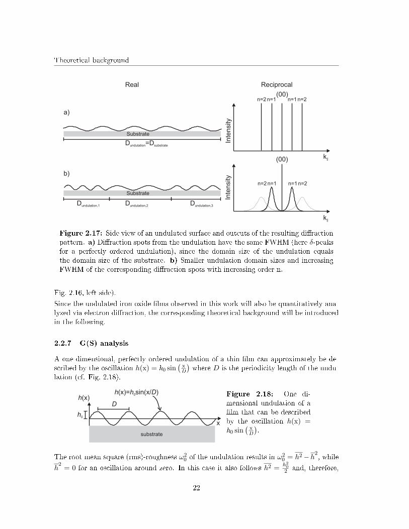
It is indicated in Fig. 2.16, that the FWHM of the di�raction spots increases with increasingdistance from the primal substrate di�raction spots. The FWHM of the di�raction spotsincreases more drastically the less the undulation is ordered (variation in periodicity). Onthe other hand, a perfectly ordered undulation would exhibit δ-shaped di�raction spots.Fig. 2.17 shows the in�uence of the order of the undulation on the corresponding di�ractionspots.
For a not perfectly ordered undulation the FWHM of the corresponding di�raction spotsincreases quadratically with the order of the spots (FWHM ∝ n2) [49, 50]. As mentionedbefore, similar to the di�raction spots caused by a superstructure the spots coming froman undulation do not change their lateral position in reciprocal space with increasingscattering phase. Hence, an undulation can be seen as a special kind of superstructure (cf.
21
Theoretical background
Real Reciprocal
D =Dundulation substrate
a)
Substrate
Dundulation,1 Dundulation,2 Dundulation,3
b)
Substrate
(00)n=1 n=2n=2 n=1
k||(00)
n=1 n=2n=2 n=1
k||
Inte
nsity
Inte
nsity
Figure 2.17: Side view of an undulated surface and outcuts of the resulting di�ractionpattern. a) Di�raction spots from the undulation have the same FWHM (here δ-peaksfor a perfectly ordered undulation), since the domain size of the undulation equalsthe domain size of the substrate. b) Smaller undulation domain sizes and increasingFWHM of the corresponding di�raction spots with increasing order n.
Fig. 2.16, left side).
Since the undulated iron oxide �lms observed in this work will also be quantitatively ana-lyzed via electron di�raction, the corresponding theoretical background will be introducedin the following.
2.2.7 G(S) analysis
A one dimensional, perfectly ordered undulation of a thin �lm can approximately be de-scribed by the oscillation h(x) = h0 sin
(xD
)where D is the periodicity length of the undu-
lation (cf. Fig. 2.18).
substrate
D
h0
x
h(x)= sin(x/ )h D0
h(x)Figure 2.18: One di-mensional undulation of a�lm that can be describedby the oscillation h(x) =h0 sin
(xD
).
The root mean square (rms)-roughness ω20 of the undulation results in ω2
0 = h2−h2, while
h2
= 0 for an oscillation around zero. In this case it also follows h2 =h202 and, therefore,
22
Theoretical background
ω0 = h0√2.
For thin Ge �lms on Si(111) and Ag �lms on Si(001) it has already been reported thatelectron di�raction can also give information about the height of such undulations [49, 50].This can be done by analysis of the behavior of the integrated satellite spot intensitiesfrom one fundamental di�raction spot, with increasing k⊥ (G(S) analysis). In general, thebehavior of the integrated intensities is described by quadratic Bessel functions Jn(x)2,where n is the order of the corresponding satellite. But in a �rst approximation the satelliteintensities show a quadratic behavior in k⊥ for very low electron energies [49]. For higherelectron energies (depending on the rms-roughness of the undulation) the intensities of thesatellite spots follow Gaussian distributions in k⊥. In this case the intensity of the centralspot decreases via
I0 = e−ω20k
2⊥ . 2.45
This relative integrated intensity is calculated with respect to the integrated intensity of thewhole di�raction spot. An increasing Gaussian distribution, on the other hand, describesthe behavior of the intensities of the satellite spots as
In = 1− e−ω2nk2⊥ , 2.46
where n > 0 is again the order of the regarding satellite spot.
Furthermore, the sum of the relative integrated intensities of all spots has to be 1. Thisleads to a dependency between the parameters ωn. In the case of �ve satellite spots (centralspot, �rst and second order satellites), this leads to
1 = e−ω20k
2⊥ + 1− e−ω
21k
2⊥ + 1− e−ω
22k
2⊥ 2.47
1 = −e−ω20k
2⊥ + e−ω
21k
2⊥ + e−ω
22k
2⊥ . 2.48
For low electron energies (small values of k⊥) the exponential functions from Eq. 2.48 canbe written as Taylor series development around ω2
nk2⊥ = 0 via
e−ω2nk2⊥ =
∞∑m=0
(−ω2nk
2⊥)m
m!. 2.49
For small values of k⊥ and since ωn < 1 for all undulations with a height of ∆h < 2.8 A(from ω0 = ∆h
2√
2) follows ω2
nk2⊥ < 1. In that case an expansion of the Taylor series up
to the �rst order already results in a very small discrepancy and is, therefore, a su�cientapproximation. We obtain
23
Theoretical background
e−ω2nk2⊥ =
1∑m=0
(−ω2nk
2⊥)m
m!= 1− ω2
nk2⊥ . 2.50
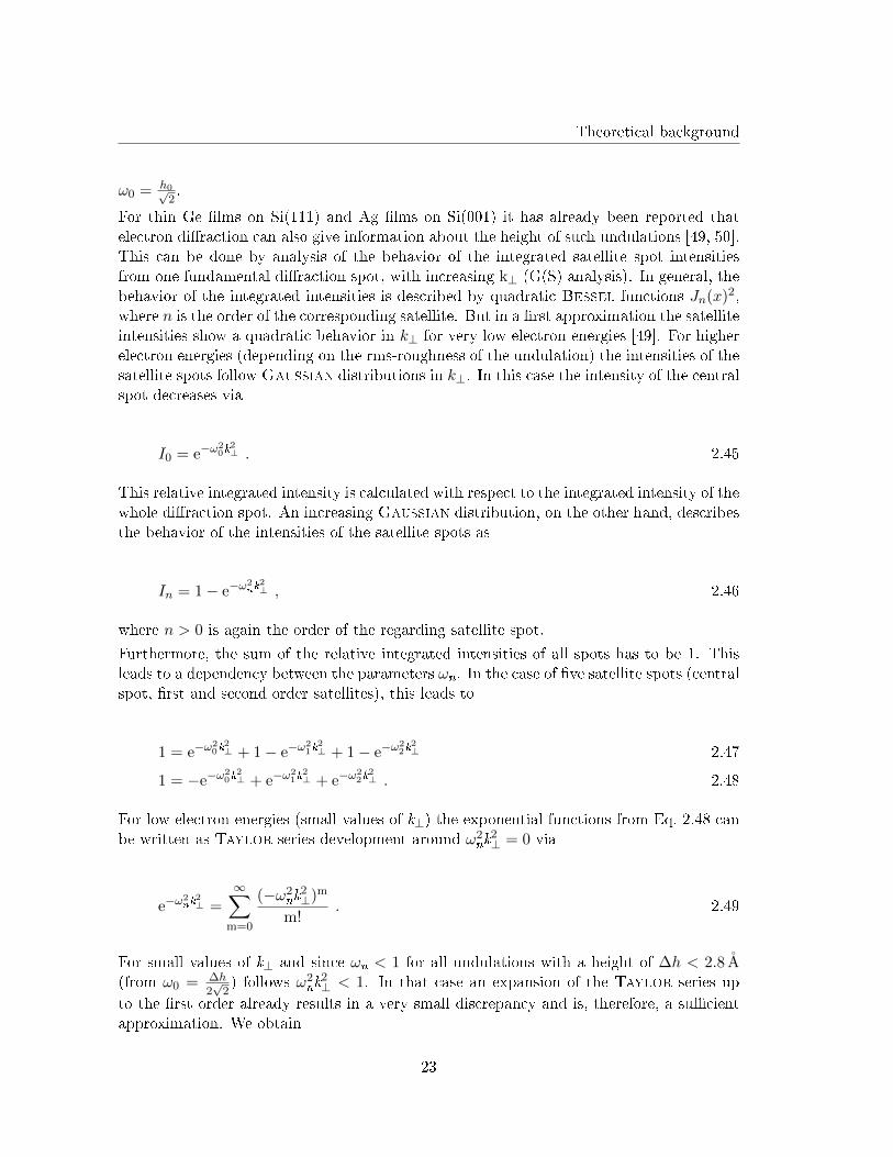
The Gaussian behavior of the integrated spot intensities plotted against k⊥ using the �rstorder Taylor series approximation is presented in Fig. 2.19 b) for satellites up to secondorder. Since the Gaussians can only serve as approximations of Bessel functions for lowelectron energies, the corresponding Bessel functions are also given in Fig. 2.19 a) forcomparison.
k⊥ [A− 1]
ω22=0.2
ω20=0.05
ω21=0.1
central spot1st order sat.2nd order sat.
J(x
)n
J0
2
J1
2
J2
2
a) b)Gaussian behavior
Figure 2.19: a) quadratic Bessel functions describing typical satellite intensity be-haviors for a long range of electron energies (represented by x values). b) TypicalGaussian behavior of the normalized spot intensities plotted against k⊥ using the �rstorder Taylor series approximation for satellites up to second order for small values ofk⊥. This approximation is valid for the region marked in a). The ωn ful�ll the condition2.53.
Using the Taylor series approximation up to �rst order one can determine a simplerelation between the ωn (satellites up to 2nd order). It is
1 = −1 + ω20k
2⊥ + 1− ω2
1k2⊥ + 1− ω2
2k2⊥ 2.51
0 = ω20k
2⊥ − ω2
1k2⊥ − ω2
2k2⊥ . 2.52
For k⊥ 6= 0 follows
ω20 = ω2
1 + ω22 . 2.53
24
Theoretical background
Relation 2.53 can be used as a condition for the description of the intensity developmentof the satellite spots in k⊥ for low electron energies.
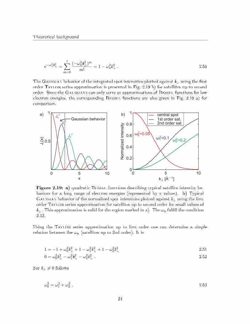
Since our di�raction experiments were performed at electron energies around 100 eV and,therefore, ω2
nk2⊥ ≈ 1, the Taylor series needs to be expanded to higher orders to minimize
the di�erence to the exponential function. In our case (ω2i k
2⊥ ≈ 1) an expansion of Eq.(2.50)
up to third order produced su�cient results (cf. Fig. 2.20).
x= =1w ki
22
Figure 2.20: Development ofthe exponential function in com-parison to the expansion of itsTaylor series up to di�erent or-ders. The discrepancy betweeny = e−x and y = 1− x+ x2
2 −x3
6is acceptably small for x ≈ 1.
The relation between the ωi is much more complicated in this case but can still be analyt-ically resolved from
1 =− 1 + ω20k
2⊥ −
ω40k
4⊥
2+ω6
0k6⊥
6
+ 1− ω21k
2⊥ +
ω41k
4⊥
2− ω6
1k6⊥
6
+ 1− ω22k
2⊥ +
ω42k
4⊥
2− ω6
2k6⊥
62.54
Hence, we used Gaussian distributions to describe the behavior of the satellite intensities.The relation between the ωi solved from Eq. 2.54 can be used as a �tting condition forthe development of the relative integrated intensities of the satellite spots with increasingelectron energies.
2.3 X-ray Photoelectron Spectroscopy
A relevant technique for the analysis of the chemical composition and the electronic struc-ture of surfaces is X-ray Photoelectron Spectroscopy (XPS). The following chapter shedssome light on this method and its theoretical basics.
25
Theoretical background
2.3.1 The photoelectrical e�ect
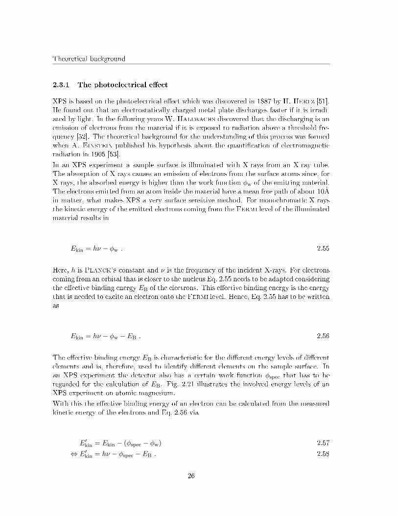
XPS is based on the photoelectrical e�ect which was discovered in 1887 by H. Hertz [51].He found out that an electrostatically charged metal plate discharges faster if it is irradi-ated by light. In the following yearsW. Hallwachs discovered that the discharging is anemission of electrons from the material if it is exposed to radiation above a threshold fre-quency [52]. The theoretical background for the understanding of this process was formedwhen A. Einstein published his hypothesis about the quanti�cation of electromagneticradiation in 1905 [53].
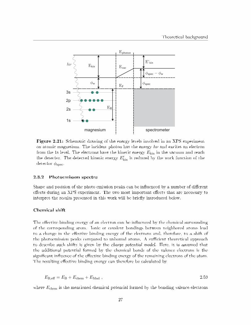
In an XPS experiment a sample surface is illuminated with X-rays from an X-ray tube.The absorption of X-rays causes an emission of electrons from the surface atoms since, forX-rays, the absorbed energy is higher than the work function φw of the emitting material.The electrons emitted from an atom inside the material have a mean free path of about 10Ain matter, what makes XPS a very surface sensitive method. For monochromatic X-raysthe kinetic energy of the emitted electrons coming from the Fermi level of the illuminatedmaterial results in
Ekin = hν − φw . 2.55
Here, h is Planck's constant and ν is the frequency of the incident X-rays. For electronscoming from an orbital that is closer to the nucleus Eq. 2.55 needs to be adapted consideringthe e�ective binding energy EB of the electrons. This e�ective binding energy is the energythat is needed to excite an electron onto the Fermi level. Hence, Eq. 2.55 has to be writtenas
Ekin = hν − φw − EB . 2.56
The e�ective binding energy EB is characteristic for the di�erent energy levels of di�erentelements and is, therefore, used to identify di�erent elements on the sample surface. Inan XPS experiment the detector also has a certain work function φspec that has to beregarded for the calculation of EB. Fig. 2.21 illustrates the involved energy levels of anXPS experiment on atomic magnesium.
With this the e�ective binding energy of an electron can be calculated from the measuredkinetic energy of the electrons and Eq. 2.56 via
E′kin = Ekin − (φspec − φw) 2.57
⇔ E′kin = hν − φspec − EB . 2.58
26
Theoretical background
2p
2s
1s
magnesium spectrometer
3s
Figure 2.21: Schematic drawing of the energy levels involved in an XPS experimenton atomic magnesium. The incident photon has the energy hν and excites an electronfrom the 1s level. The electrons have the kinetic energy Ekin in the vacuum and reachthe detector. The detected kinetic energy E′kin is reduced by the work function of thedetector φspec.
2.3.2 Photoemisson spectra
Shape and position of the photo emission peaks can be in�uenced by a number of di�erente�ects during an XPS experiment. The two most important e�ects that are necessary tointerpret the results presented in this work will be brie�y introduced below.
Chemical shift
The e�ective binding energy of an electron can be in�uenced by the chemical surroundingof the corresponding atom. Ionic or covalent bondings between neighbored atoms leadto a change in the e�ective binding energy of the electrons and, therefore, to a shift ofthe photoemission peaks compared to unbound atoms. A su�cient theoretical approachto describe such shifts is given by the charge potential model. Here, it is assumed thatthe additional potential formed by the chemical bonds of the valence electrons is thesigni�cant in�uence of the e�ective binding energy of the remaining electrons of the atom.The resulting e�ective binding energy can therefore be calculated by
EB,eff = EB + Echem + EMad , 2.59
where Echem is the mentioned chemical potential formed by the bonding valence electrons
27
Theoretical background
and EMad is the Madelung term summing up the potentials of the surrounding atoms.In practice, reference spectra from known compositions are taken from literature and com-pared to the measured spectra [54].
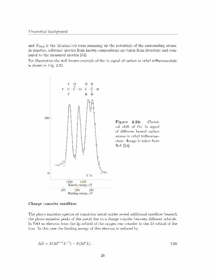
For illustration the well known example of the 1s signal of carbon in ethyl tri�uoroacetateis shown in Fig. 2.22.
Figure 2.22: Chemi-cal shift of the 1s signalof di�erent bound carbonatoms in ethyl tri�uoroac-etate. Image is taken fromRef. [55].
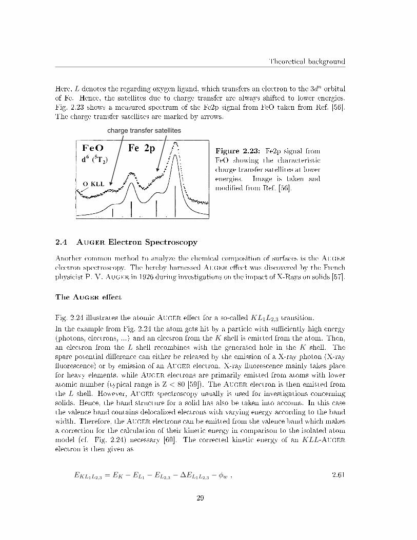
Charge transfer satellites
The photo emission spectra of transition metal oxides reveal additional satellites beneaththe photo emission peaks of the metal due to a charge transfer between di�erent orbitals.In FeO an electron from the 2p orbital of the oxygen can transfer to the 3d orbital of theiron. In this case the binding energy of this electron is reduced by
∆E = E(3dn+1L−1)− E(3dnL) . 2.60
28
Theoretical background
Here, L denotes the regarding oxygen ligand, which transfers an electron to the 3dn orbitalof Fe. Hence, the satellites due to charge transfer are always shifted to lower energies.Fig. 2.23 shows a measured spectrum of the Fe2p signal from FeO taken from Ref. [56].The charge transfer satellites are marked by arrows.
charge transfer satellites
Figure 2.23: Fe2p signal fromFeO showing the characteristiccharge transfer satellites at lowerenergies. Image is taken andmodi�ed from Ref. [56].
2.4 Auger Electron Spectroscopy
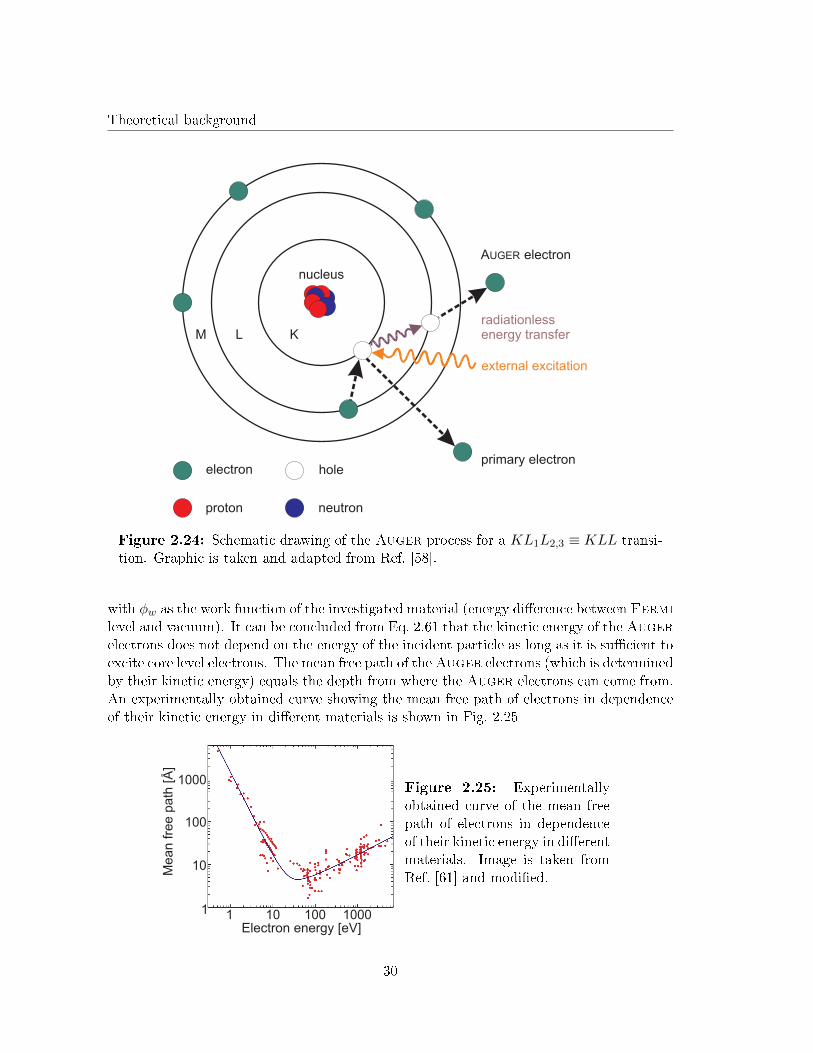
Another common method to analyze the chemical composition of surfaces is the Augerelectron spectroscopy. The hereby harnessed Auger e�ect was discovered by the Frenchphysicist P. V. Auger in 1926 during investigations on the impact of X-Rays on solids [57].
The Auger e�ect
Fig. 2.24 illustrates the atomic Auger e�ect for a so-called KL1L2,3 transition.
In the example from Fig. 2.24 the atom gets hit by a particle with su�ciently high energy(photons, electrons, ...) and an electron from the K shell is emitted from the atom. Then,an electron from the L shell recombines with the generated hole in the K shell. Thespare potential di�erence can either be released by the emission of a X-ray photon (X-ray�uorescence) or by emission of an Auger electron. X-ray �uorescence mainly takes placefor heavy elements, while Auger electrons are primarily emitted from atoms with loweratomic number (typical range is Z < 80 [59]). The Auger electron is then emitted fromthe L shell. However, Auger spectroscopy usually is used for investigations concerningsolids. Hence, the band structure for a solid has also be taken into account. In this casethe valence band contains delocalized electrons with varying energy according to the bandwidth. Therefore, the Auger electrons can be emitted from the valence band which makesa correction for the calculation of their kinetic energy in comparison to the isolated atommodel (cf. Fig. 2.24) necessary [60]. The corrected kinetic energy of an KLL-Augerelectron is then given as
EKL1L2,3 = EK − EL1 − EL2,3 −∆EL1L2,3 − φw , 2.61
29
Theoretical background
KLM
nucleus
electron
proton neutron
hole
external excitation
primary electron
A electronUGER
radiationlessenergy transfer
Figure 2.24: Schematic drawing of the Auger process for a KL1L2,3 ≡ KLL transi-tion. Graphic is taken and adapted from Ref. [58].
with φw as the work function of the investigated material (energy di�erence between Fermilevel and vacuum). It can be concluded from Eq. 2.61 that the kinetic energy of the Augerelectrons does not depend on the energy of the incident particle as long as it is su�cient toexcite core level electrons. The mean free path of theAuger electrons (which is determinedby their kinetic energy) equals the depth from where the Auger electrons can come from.An experimentally obtained curve showing the mean free path of electrons in dependenceof their kinetic energy in di�erent materials is shown in Fig. 2.25
1 10 100 10001
10
100
1000
Electron energy [eV]
Mean fre
e p
ath
[Å
]
Figure 2.25: Experimentallyobtained curve of the mean freepath of electrons in dependenceof their kinetic energy in di�erentmaterials. Image is taken fromRef. [61] and modi�ed.
30
Theoretical background
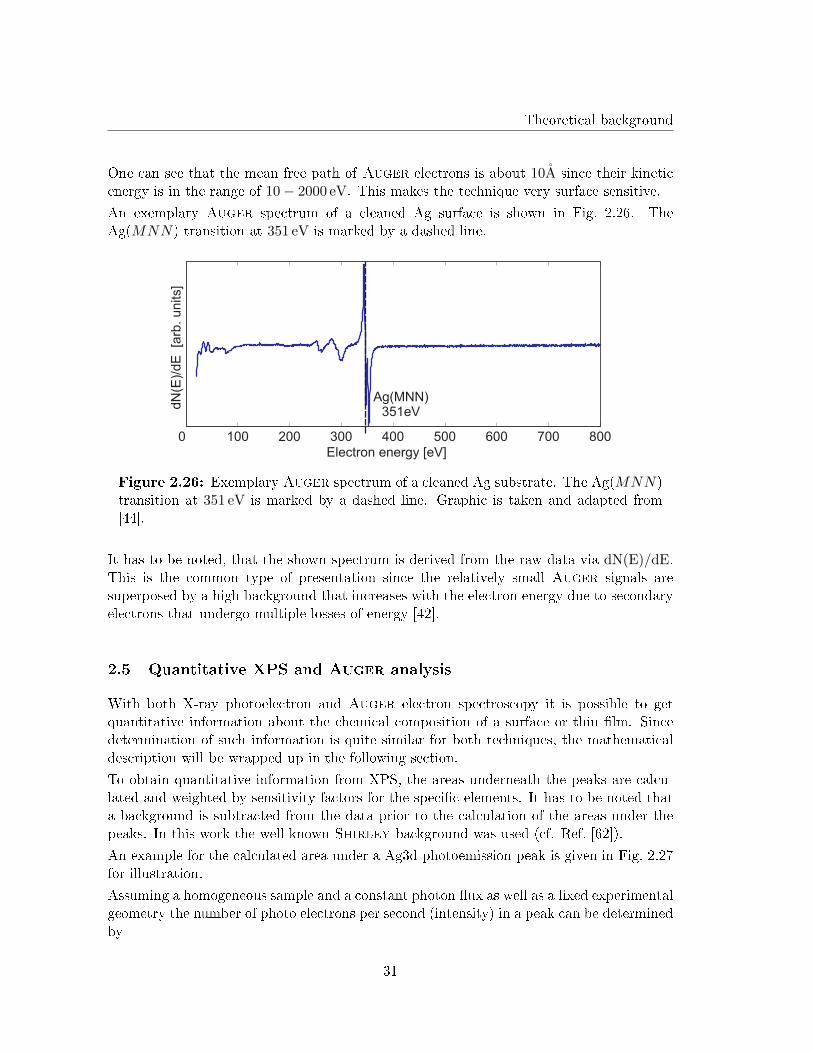
One can see that the mean free path of Auger electrons is about 10A since their kineticenergy is in the range of 10− 2000 eV. This makes the technique very surface sensitive.
An exemplary Auger spectrum of a cleaned Ag surface is shown in Fig. 2.26. TheAg(MNN) transition at 351 eV is marked by a dashed line.
0 100 200 300 400 500 600 700 800
Electron energy [eV]
dN
(E)/
dE
[a
rb. units]
Ag(MNN)351eV
Figure 2.26: Exemplary Auger spectrum of a cleaned Ag substrate. The Ag(MNN)transition at 351 eV is marked by a dashed line. Graphic is taken and adapted from[44].
It has to be noted, that the shown spectrum is derived from the raw data via dN(E)/dE.This is the common type of presentation since the relatively small Auger signals aresuperposed by a high background that increases with the electron energy due to secondaryelectrons that undergo multiple losses of energy [42].
2.5 Quantitative XPS and Auger analysis
With both X-ray photoelectron and Auger electron spectroscopy it is possible to getquantitative information about the chemical composition of a surface or thin �lm. Sincedetermination of such information is quite similar for both techniques, the mathematicaldescription will be wrapped up in the following section.
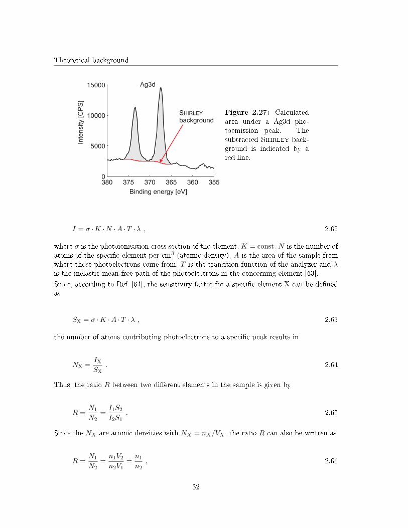
To obtain quantitative information from XPS, the areas underneath the peaks are calcu-lated and weighted by sensitivity factors for the speci�c elements. It has to be noted thata background is subtracted from the data prior to the calculation of the areas under thepeaks. In this work the well known Shirley background was used (cf. Ref. [62]).
An example for the calculated area under a Ag3d photoemission peak is given in Fig. 2.27for illustration.
Assuming a homogeneous sample and a constant photon �ux as well as a �xed experimentalgeometry the number of photo electrons per second (intensity) in a peak can be determinedby
31
Theoretical background
Binding energy [eV]
Inte
nsity [C
PS
]Ag3d
Sbackground
HIRLEY Figure 2.27: Calculatedarea under a Ag3d pho-toemission peak. Thesubtracted Shirley back-ground is indicated by ared line.
I = σ ·K ·N ·A ·T ·λ , 2.62
where σ is the photoionisation cross section of the element, K = const, N is the number ofatoms of the speci�c element per cm3 (atomic density), A is the area of the sample fromwhere those photoelectrons come from, T is the transition function of the analyzer and λis the inelastic mean-free path of the photoelectrons in the concerning element [63].
Since, according to Ref. [64], the sensitivity factor for a speci�c element X can be de�nedas
SX = σ ·K ·A ·T ·λ , 2.63
the number of atoms contributing photoelectrons to a speci�c peak results in
NX =IX
SX. 2.64
Thus, the ratio R between two di�erent elements in the sample is given by
R =N1
N2=I1S2
I2S1. 2.65
Since the NX are atomic densities with NX = nX/VX , the ratio R can also be written as
R =N1
N2=n1V2
n2V1=n1
n2, 2.66
32
Theoretical background
because V1 = V2. From Eq. 2.65 and 2.66 follows
I1S2
I2S1=n1
n2. 2.67
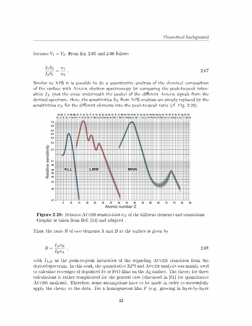
Similar to XPS it is possible to do a quantitative analysis of the chemical compositionof the surface with Auger electron spectroscopy by comparing the peak-to-peak inten-sities IX (not the areas underneath the peaks) of the di�erent Auger signals from thederived spectrum. Here, the sensitivities SX from XPS analysis are simply replaced by thesensitivities σX for the di�erent elements into the peak-to-peak ratio (cf. Fig. 2.28).
Atomic number Z
Rela
tive s
ensitiv
ity
Figure 2.28: RelativeAuger sensitivities σX of the di�erent elements and transitions.Graphic is taken from Ref. [44] and adapted .
Thus, the ratio R of two elements A and B at the surface is given by
R =IAσB
IBσA, 2.68
with IA,B as the peak-to-peak intensities of the regarding Auger transition from thederived spectrum. In this work, the quantitative XPS and Auger analysis was mainly usedto calculate coverages of deposited Fe or FeO �lms on the Ag surface. The theory for thosecalculations is rather complicated for the general case (discussed in [61] for quantitativeAuger analysis). Therefore, some assumptions have to be made in order to successfullyapply the theory to the data. For a homogeneous �lm F (e.g. growing in layer-by-layer
33
Theoretical background
mode) on the substrate S the normalized intensity ratio Irel can be written according toRef. [42] as
Irel =IF/σF
IS/σS + IF/σF= 1− e−D/λF . 2.69
Here, D is the �lm thickness, λF ≈ λS = λ is the mean free path of electrons in the mate-rial, which is approximately the same for the �lm and substrate (cf. Fig. 2.25), while σS andσF are the sensitivities of substrate and �lm, respectively (remember di�erent sensitivitiesfor AES and XPS). In the experiments performed during this work the mass equivalentevaporated onto the substrate is measured by an oscillating quartz. For a layer-by-layergrowing �lm the thickness results in D = c ·∆f where ∆f is the change in frequency ofthe oscillation quartz and c = const. Thus, by measuring the (Auger or photoemission)intensities of �lm and substrate signals for di�erent coverages Θ the unknown constant cand, therefore, the absolute �lm thickness D can be estimated using Eq. 2.69.
2.6 Scanning Tunneling Microscopy
The scanning tunneling microscopy (STM) was developed by G. Binnig, H. Rohrer,Ch. Gerber, and E. Weibel in 1982 and is, therefore, a very young surface analysismethod [65]. It was the �rst method that was able to image surface topography andelectronic structure on an atomic scale at the same time. G. Binnig and H. Rohrer
were decorated with the Nobel price for their work in 1986.
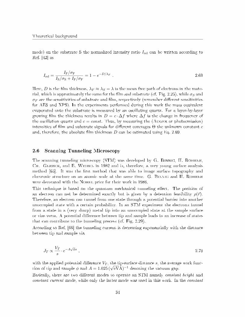
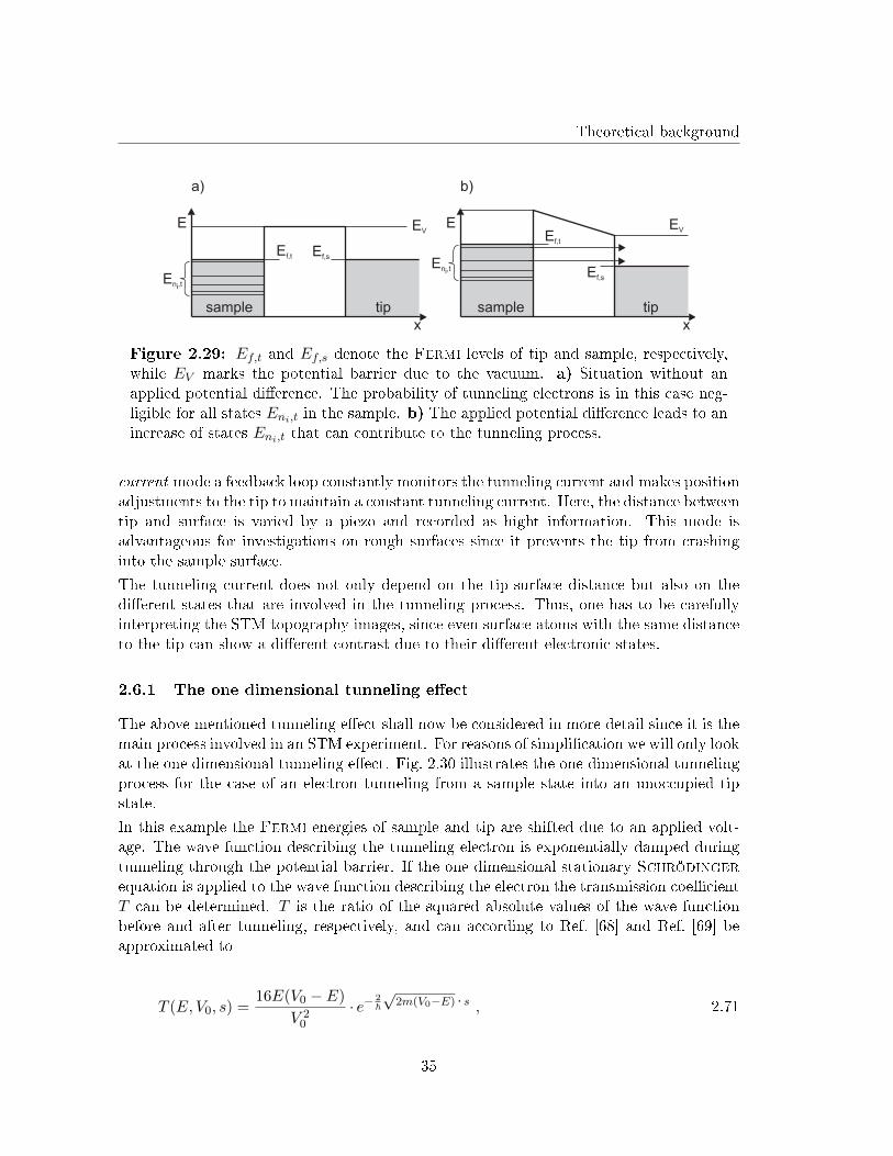
This technique is based on the quantum mechanical tunneling e�ect. The position ofan electron can not be determined exactly but is given by a detention feasibility ρ(~r).Therefore, an electron can tunnel from one state through a potential barrier into anotherunoccupied state with a certain probability. In an STM experiment the electrons tunnelfrom a state in a (very sharp) metal tip into an unoccupied state at the sample surfaceor vise versa. A potential di�erence between tip and sample leads to an increase of statesthat can contribute to the tunneling process (cf. Fig. 2.29).
According to Ref. [66] the tunneling current is decreasing exponentially with the distancebetween tip and sample via
JT ∝VTs· e−A
√φs , 2.70
with the applied potential di�erence VT , the tip-surface distance s, the average work func-tion of tip and sample φ and A = 1.025 (
√eVA)−1 denoting the vacuum gap.
Basically, there are two di�erent modes to operate an STM namely constant height andconstant current mode, while only the latter mode was used in this work. In the constant
34
Theoretical background
tipsample
E
x
EV
Ef,t Ef,s
E
x
EV
Ef,t
Ef,s
tipsample
Eni,t
Eni,t
a) b)
Figure 2.29: Ef,t and Ef,s denote the Fermi levels of tip and sample, respectively,while EV marks the potential barrier due to the vacuum. a) Situation without anapplied potential di�erence. The probability of tunneling electrons is in this case neg-ligible for all states Eni,t in the sample. b) The applied potential di�erence leads to anincrease of states Eni,t that can contribute to the tunneling process.
current mode a feedback loop constantly monitors the tunneling current and makes positionadjustments to the tip to maintain a constant tunneling current. Here, the distance betweentip and surface is varied by a piezo and recorded as hight information. This mode isadvantageous for investigations on rough surfaces since it prevents the tip from crashinginto the sample surface.
The tunneling current does not only depend on the tip-surface distance but also on thedi�erent states that are involved in the tunneling process. Thus, one has to be carefullyinterpreting the STM topography images, since even surface atoms with the same distanceto the tip can show a di�erent contrast due to their di�erent electronic states.
2.6.1 The one dimensional tunneling e�ect
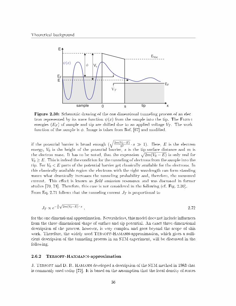
The above mentioned tunneling e�ect shall now be considered in more detail since it is themain process involved in an STM experiment. For reasons of simpli�cation we will only lookat the one dimensional tunneling e�ect. Fig. 2.30 illustrates the one dimensional tunnelingprocess for the case of an electron tunneling from a sample state into an unoccupied tipstate.
In this example the Fermi energies of sample and tip are shifted due to an applied volt-age. The wave function describing the tunneling electron is exponentially damped duringtunneling through the potential barrier. If the one dimensional stationary Schrödingerequation is applied to the wave function describing the electron the transmission coe�cientT can be determined. T is the ratio of the squared absolute values of the wave functionbefore and after tunneling, respectively, and can according to Ref. [68] and Ref. [69] beapproximated to
T (E, V0, s) =16E(V0 − E)
V 20
· e−2~
√2m(V0−E) · s , 2.71
35
Theoretical background
sample 0 s tip
E
x
E
V0
Figure 2.30: Schematic drawing of the one dimensional tunneling process of an elec-tron represented by its wave function ψ(x) from the sample into the tip. The Fermienergies (EF ) of sample and tip are shifted due to an applied voltage VT . The workfunction of the sample is φ. Image is taken from Ref. [67] and modi�ed.
if the potential barrier is broad enough (√
2m(V0−E)~2 · s � 1). Here, E is the electron
energy, V0 is the height of the potential barrier, s is the tip-surface distance and m isthe electron mass. It has to be noted, that the expression
√2m(V0 − E) is only real for
V0 ≥ E. This is indeed the condition for the tunneling of electrons from the sample into thetip. For V0 < E parts of the potential barrier get classically available for the electrons. Inthis classically available region the electrons with the right wavelength can form standingwaves what drastically increases the tunneling probability and, therefore, the measuredcurrent. This e�ect is known as �eld emission resonance and was discussed in formerstudies [70, 71]. Therefore, this case is not considered in the following (cf. Fig. 2.30).
From Eq. 2.71 follows that the tunneling current JT is proportional to
JT ∝ e−2~
√2m(V0−E) · s , 2.72
for the one dimensional approximation. Nevertheless, this model does not include in�uencesfrom the three dimensional shape of surface and tip potential. An exact three dimensionaldescription of the process, however, is very complex and goes beyond the scope of thiswork. Therefore, the widely used Tersoff-Hamann-approximation, which gives a su�-cient description of the tunneling process in an STM experiment, will be discussed in thefollowing.
2.6.2 Tersoff-Harmann-approximation
J. Tersoff and D. R. Hamann developed a description of the STM method in 1983 thatis commonly used today [72]. It is based on the assumption that the local density of states
36
Theoretical background
ρT (EF ) is maximal at the top atom of the tip where the distance to the sample is thesmallest. Only this top atom contributes to the tunneling process and its wave functionis assumed to be spherical (s-wave funktion). The approximation uses the many-particletunneling theory from Bardeen [73]. Gottlieb at al. applied Bardeen's theory toscanning tunneling microscopy [74], where the tunneling current can be described via
JT =4πe
~
∫ eVT
0ρ0(EF − eVT + ε)ρT (EF + ε)|M |2dε , 2.73
with the density of states at the tip ρT (E) and at the surface ρ0(E) and the applied voltageVT . |M |2 is the transition matrix which contains the wave functions of sample and tip (cf.Ref. [73]). With this formalism Tersoff and Hamann found that the tunneling currentis only depending on the density of Fermi level states at the surface point that is closestto the tip with
JT ∝ VTρsurf(R,EF ) . 2.74
Here, R is the position of the topmost atom at the tip over the sample surface, EF is theFermi energy at the corresponding surface position and VT is the applied potential atthe tip. Eq. 2.74 shows one more time that an STM image is not an actual topographicillustration of the sample surface but a mapping of the density of states.
2.6.3 Topographic height measurements in STM
Since we will also estimate topographic heights from our STM measurements, we wouldlike to brie�y address some non-topographic e�ects that can lead to a change in contrastduring an STM measurement. Here, we present some STM measurements on reactivelygrown FeO �lms on Ag(001) as examples. These �lms, however, will be discussed inChap. 5.5 in detail.
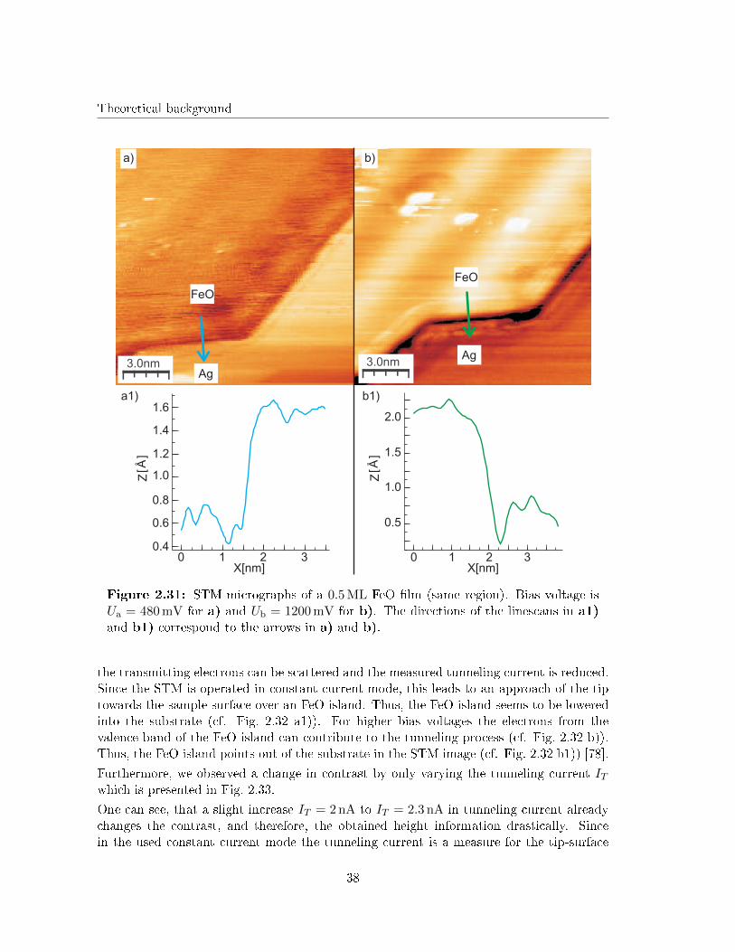
It is well known from literature, that di�erent bias voltages can lead to a change in con-trast in an STM image [75, 76, 77]. The reason for this is the increasing number ofelectronic states that can contribute to the tunneling process with increasing bias voltage(cf. Chap. 2.6). As shown in Fig. 2.31, we changed the bias voltage during one series ofmeasurements to analyze the in�uence on the image contrast.
As predicted in other studies [75, 76, 77] a changing bias voltage leads to an inversion ofcontrast in our case. The FeO island in Fig. 2.31 a) seems to be lowered into the substrate,while the same island points out of the sample surface in Fig. 2.31 b).
This e�ect was already reported for the growth of NiO on Ag(001) by Sebastian et al. [78]and can be illustrated by the model shown in Fig. 2.32.
Using low bias voltages only the electrons from the states of the Ag substrate can contributeto the tunneling process (cf. Fig. 2.32 a)). In the FeO islands on top of the Ag substrate
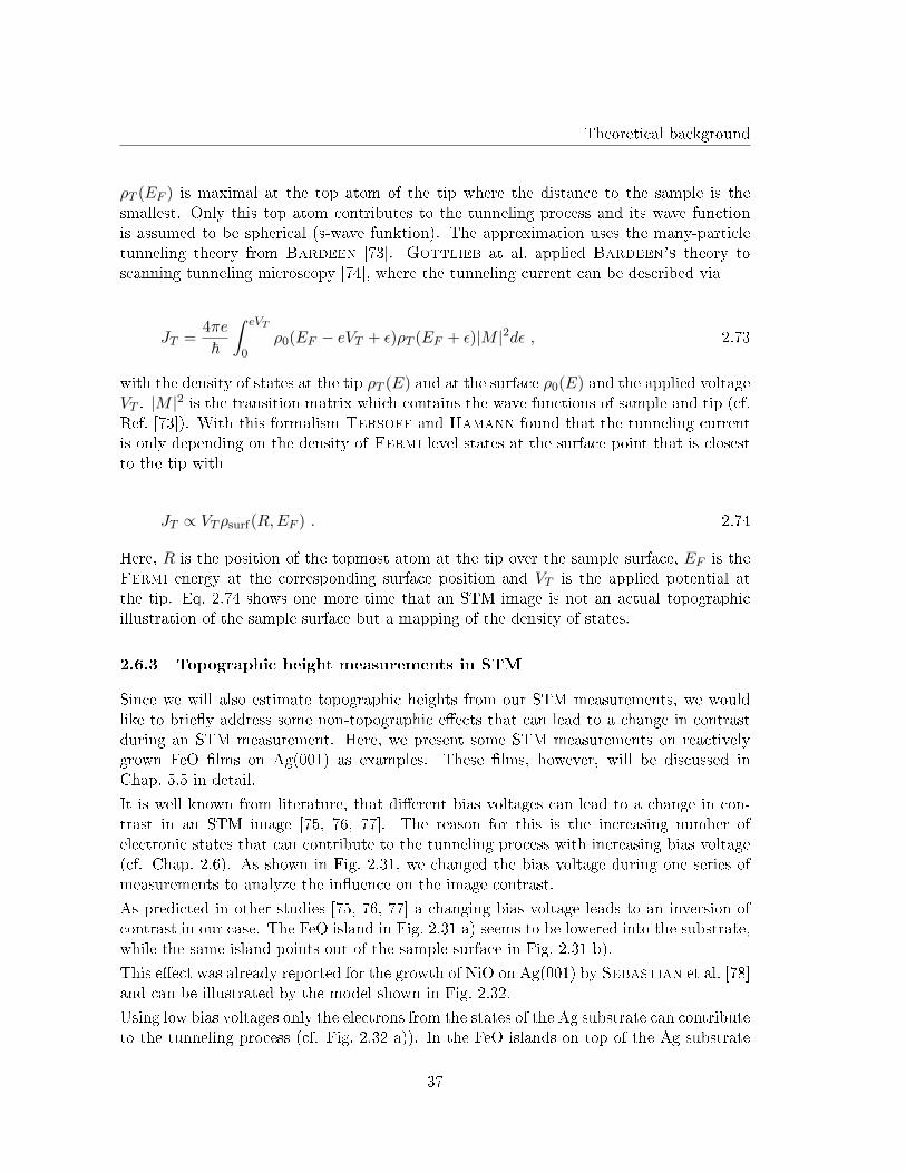
37
Theoretical background
3210
2.0
1.5
1.0
0.5
X[nm]
Z[Å
]
3210X[nm]
1.6
1.4
1.2
1.0
0.8
0.6
0.4
Z[Å
]
a1) b1)
3.0nm 3.0nm
a) b)
FeO
FeO
Ag
Ag
Figure 2.31: STM micrographs of a 0.5 ML FeO �lm (same region). Bias voltage isUa = 480 mV for a) and Ub = 1200 mV for b). The directions of the linescans in a1)and b1) correspond to the arrows in a) and b).
the transmitting electrons can be scattered and the measured tunneling current is reduced.Since the STM is operated in constant current mode, this leads to an approach of the tiptowards the sample surface over an FeO island. Thus, the FeO island seems to be loweredinto the substrate (cf. Fig. 2.32 a1)). For higher bias voltages the electrons from thevalence band of the FeO island can contribute to the tunneling process (cf. Fig. 2.32 b)).Thus, the FeO island points out of the substrate in the STM image (cf. Fig. 2.32 b1)) [78].
Furthermore, we observed a change in contrast by only varying the tunneling current ITwhich is presented in Fig. 2.33.
One can see, that a slight increase IT = 2 nA to IT = 2.3 nA in tunneling current alreadychanges the contrast, and therefore, the obtained height information drastically. Sincein the used constant current mode the tunneling current is a measure for the tip-surface
38
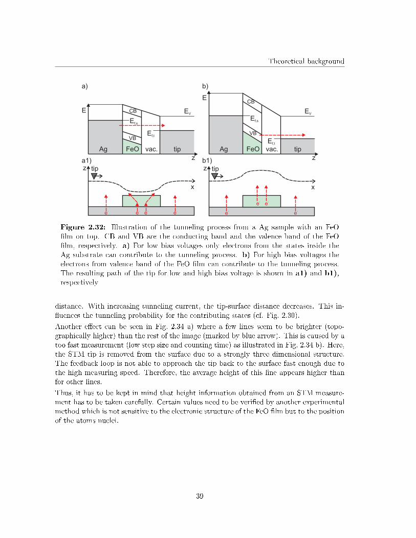
Theoretical background
E
z
EV
Ef,s
Ef,t
Ag tip
a)
FeO
VB
CB
vac.
E
z
Ef,s
Ef,t
Ag tip
b)
FeO
VB
CB
vac.
tip
e-
e-
e-
e-
a1)
x
z tip
e-
e-
e-
e-
x
zb1)
EV
Figure 2.32: Illustration of the tunneling process from a Ag sample with an FeO�lm on top. CB and VB are the conducting band and the valence band of the FeO�lm, respectively. a) For low bias voltages only electrons from the states inside theAg substrate can contribute to the tunneling process. b) For high bias voltages theelectrons from valence band of the FeO �lm can contribute to the tunneling process.The resulting path of the tip for low and high bias voltage is shown in a1) and b1),respectively
distance. With increasing tunneling current, the tip-surface distance decreases. This in-�uences the tunneling probability for the contributing states (cf. Fig. 2.30).
Another e�ect can be seen in Fig. 2.34 a) where a few lines seem to be brighter (topo-graphically higher) than the rest of the image (marked by blue arrow). This is caused by atoo fast measurement (low step size and counting time) as illustrated in Fig. 2.34 b). Here,the STM tip is removed from the surface due to a strongly three dimensional structure.The feedback loop is not able to approach the tip back to the surface fast enough due tothe high measuring speed. Therefore, the average height of this line appears higher thanfor other lines.
Thus, it has to be kept in mind that height information obtained from an STM measure-ment has to be taken carefully. Certain values need to be veri�ed by another experimentalmethod which is not sensitive to the electronic structure of the FeO �lm but to the positionof the atoms nuclei.
39
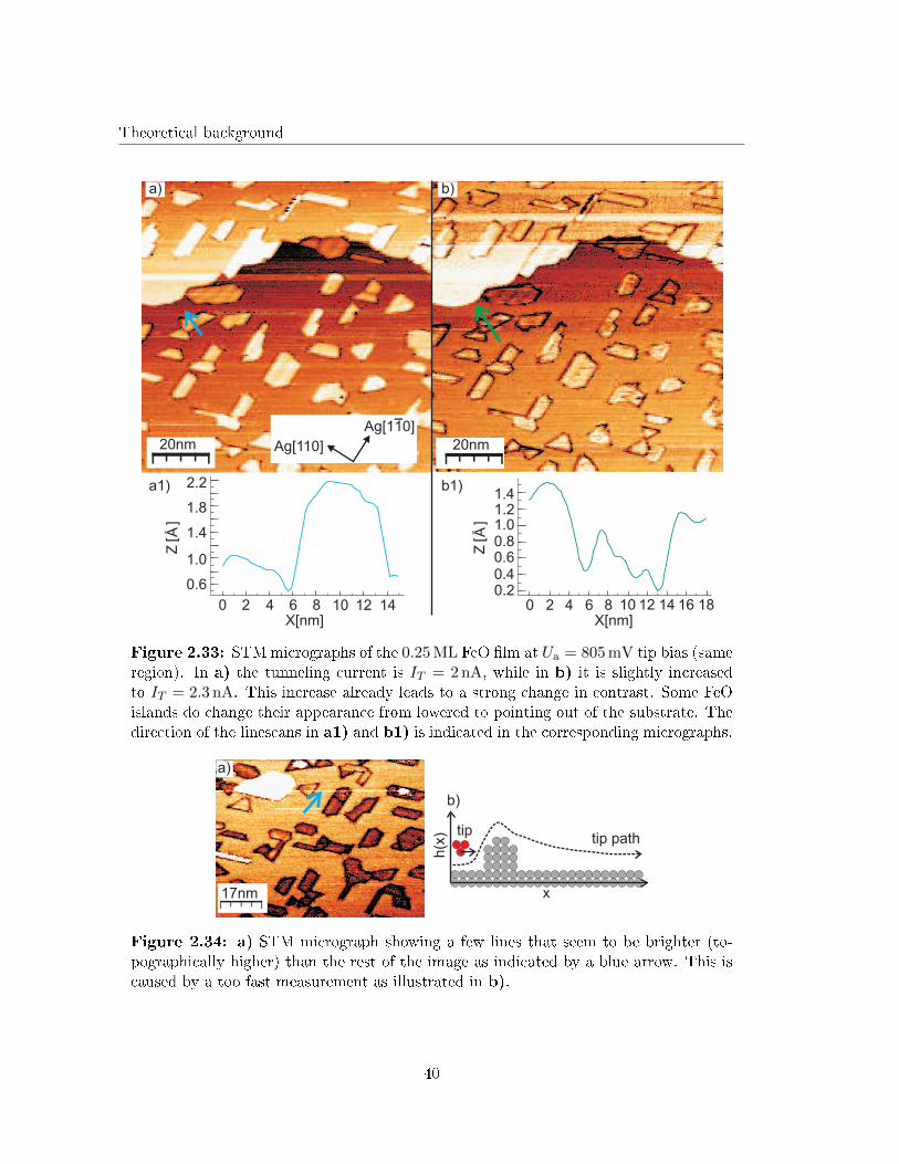
Theoretical background
181614121086420
1.41.21.00.80.60.40.2
X[nm]
Z[ Å
]
14121086420
2.2
1.8
1.4
1.0
0.6
Z[ Å
]
X[nm]
20nm 20nmAg[110]
Ag[1 0]1
a) b)
a1) b1)
Figure 2.33: STMmicrographs of the 0.25 ML FeO �lm at Ua = 805 mV tip bias (sameregion). In a) the tunneling current is IT = 2 nA, while in b) it is slightly increasedto IT = 2.3 nA. This increase already leads to a strong change in contrast. Some FeOislands do change their appearance from lowered to pointing out of the substrate. Thedirection of the linescans in a1) and b1) is indicated in the corresponding micrographs.
17nm
a)
b)
tip
h(x
)
x
tip path
Figure 2.34: a) STM micrograph showing a few lines that seem to be brighter (to-pographically higher) than the rest of the image as indicated by a blue arrow. This iscaused by a too fast measurement as illustrated in b).
40
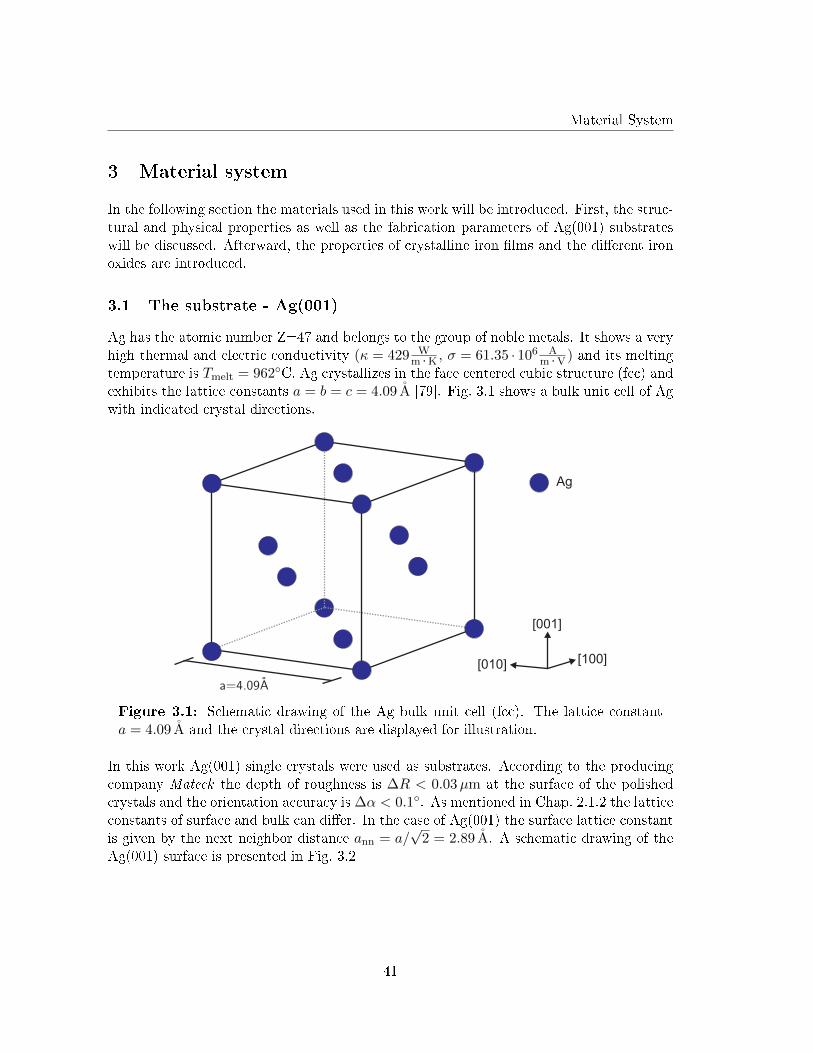
Material System
3 Material system
In the following section the materials used in this work will be introduced. First, the struc-tural and physical properties as well as the fabrication parameters of Ag(001) substrateswill be discussed. Afterward, the properties of crystalline iron �lms and the di�erent ironoxides are introduced.
3.1 The substrate - Ag(001)
Ag has the atomic number Z=47 and belongs to the group of noble metals. It shows a veryhigh thermal and electric conductivity (κ = 429 W
m ·K , σ = 61.35 · 106 Am ·V ) and its melting
temperature is Tmelt = 962◦C. Ag crystallizes in the face centered cubic structure (fcc) andexhibits the lattice constants a = b = c = 4.09 A [79]. Fig. 3.1 shows a bulk unit cell of Agwith indicated crystal directions.
[001]
[100]
Ag
[010]
Figure 3.1: Schematic drawing of the Ag bulk unit cell (fcc). The lattice constanta = 4.09 A and the crystal directions are displayed for illustration.
In this work Ag(001) single crystals were used as substrates. According to the producingcompany Mateck the depth of roughness is ∆R < 0.03µm at the surface of the polishedcrystals and the orientation accuracy is ∆α < 0.1◦. As mentioned in Chap. 2.1.2 the latticeconstants of surface and bulk can di�er. In the case of Ag(001) the surface lattice constantis given by the next neighbor distance ann = a/
√2 = 2.89 A. A schematic drawing of the
Ag(001) surface is presented in Fig. 3.2
41
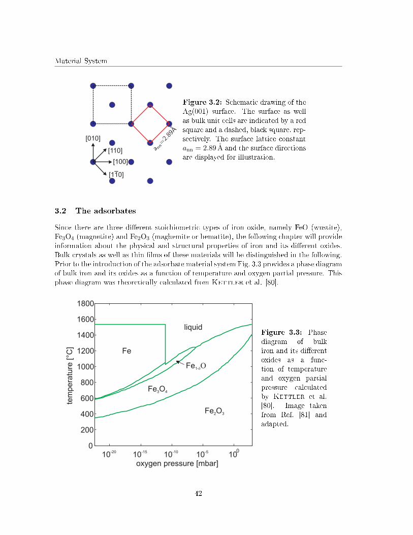
Material System
[010]
[100]
[110]
[1 0]1
Figure 3.2: Schematic drawing of theAg(001) surface. The surface as wellas bulk unit cells are indicated by a redsquare and a dashed, black square, rep-sectively. The surface lattice constantann = 2.89 A and the surface directionsare displayed for illustration.
3.2 The adsorbates
Since there are three di�erent stoichiometric types of iron oxide, namely FeO (wustite),Fe3O4 (magnetite) and Fe2O3 (maghemite or hematite), the following chapter will provideinformation about the physical and structural properties of iron and its di�erent oxides.Bulk crystals as well as thin �lms of these materials will be distinguished in the following.Prior to the introduction of the adsorbate material system Fig. 3.3 provides a phase diagramof bulk iron and its oxides as a function of temperature and oxygen partial pressure. Thisphase diagram was theoretically calculated from Kettler et al. [80].
10-20
10-15
10-10
10-5
100
0
200
400
600
800
1000
1200
1400
1600
1800
oxygen pressure [mbar]
Fe
liquid
tem
pe
ratu
re [
°C]
Fe1-dO
Fe O3 4
Fe O2 3
Figure 3.3: Phasediagram of bulkiron and its di�erentoxides as a func-tion of temperatureand oxygen partialpressure calculatedby Kettler et al.[80]. Image takenfrom Ref. [81] andadapted.
42
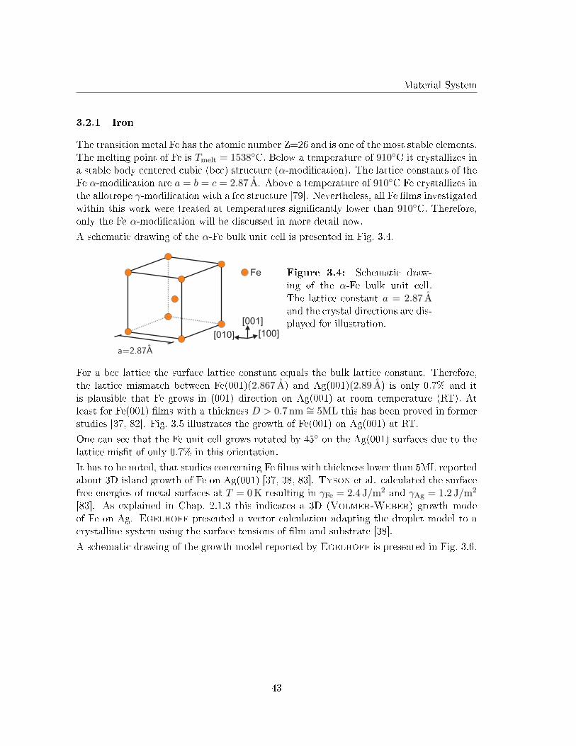
Material System
3.2.1 Iron
The transition metal Fe has the atomic number Z=26 and is one of the most stable elements.The melting point of Fe is Tmelt = 1538◦C. Below a temperature of 910◦C it crystallizes ina stable body centered cubic (bcc) structure (α-modi�cation). The lattice constants of theFe α-modi�cation are a = b = c = 2.87 A. Above a temperature of 910◦C Fe crystallizes inthe allotrope γ-modi�cation with a fcc structure [79]. Nevertheless, all Fe �lms investigatedwithin this work were treated at temperatures signi�cantly lower than 910◦C. Therefore,only the Fe α-modi�cation will be discussed in more detail now.
A schematic drawing of the α-Fe bulk unit cell is presented in Fig. 3.4.
[001]
[100]
Fe
[010]
Figure 3.4: Schematic draw-ing of the α-Fe bulk unit cell.The lattice constant a = 2.87 Aand the crystal directions are dis-played for illustration.
For a bcc lattice the surface lattice constant equals the bulk lattice constant. Therefore,the lattice mismatch between Fe(001)(2.867 A) and Ag(001)(2.89 A) is only 0.7% and itis plausible that Fe grows in (001) direction on Ag(001) at room temperature (RT). Atleast for Fe(001) �lms with a thickness D > 0.7 nm ∼= 5ML this has been proved in formerstudies [37, 82]. Fig. 3.5 illustrates the growth of Fe(001) on Ag(001) at RT.
One can see that the Fe unit cell grows rotated by 45◦ on the Ag(001) surfaces due to thelattice mis�t of only 0.7% in this orientation.
It has to be noted, that studies concerning Fe �lms with thickness lower than 5ML reportedabout 3D island growth of Fe on Ag(001) [37, 38, 83]. Tyson et al. calculated the surfacefree energies of metal surfaces at T = 0 K resulting in γFe = 2.4 J/m2 and γAg = 1.2 J/m2
[83]. As explained in Chap. 2.1.3 this indicates a 3D (Volmer-Weber) growth modeof Fe on Ag. Egelhoff presented a vector calculation adapting the droplet model to acrystalline system using the surface tensions of �lm and substrate [38].
A schematic drawing of the growth model reported by Egelhoff is presented in Fig. 3.6.
43
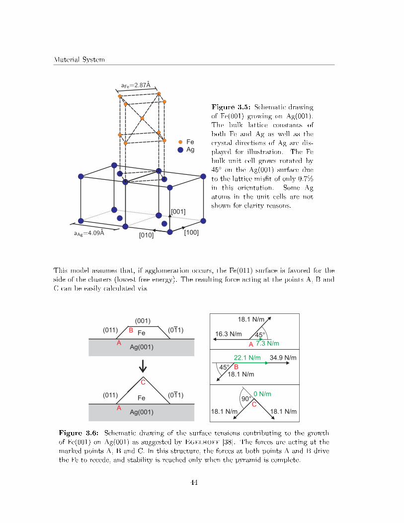
Material System
[001]
[100]
Ag
[010]
Fe
Figure 3.5: Schematic drawingof Fe(001) growing on Ag(001).The bulk lattice constants ofboth Fe and Ag as well as thecrystal directions of Ag are dis-played for illustration. The Febulk unit cell grows rotated by45◦ on the Ag(001) surface dueto the lattice mis�t of only 0.7%in this orientation. Some Agatoms in the unit cells are notshown for clarity reasons.
This model assumes that, if agglomeration occurs, the Fe(011) surface is favored for theside of the clusters (lowest free energy). The resulting force acting at the points A, B andC can be easily calculated via
(011) (0 1)1
(001)
Ag(001)
Fe 45°16.3 N/m
18.1 N/m
A
B
A 7.3 N/m
18.1 N/m
34.9 N/m
45°
22.1 N/m
B
(011) (0 1)1
Ag(001)
Fe
A
C
90°0 N/m
18.1 N/m18.1 N/mC
Figure 3.6: Schematic drawing of the surface tensions contributing to the growthof Fe(001) on Ag(001) as suggested by Egelhoff [38]. The forces are acting at themarked points A, B and C. In this structure, the forces at both points A and B drivethe Fe to recede, and stability is reached only when the pyramid is complete.
44
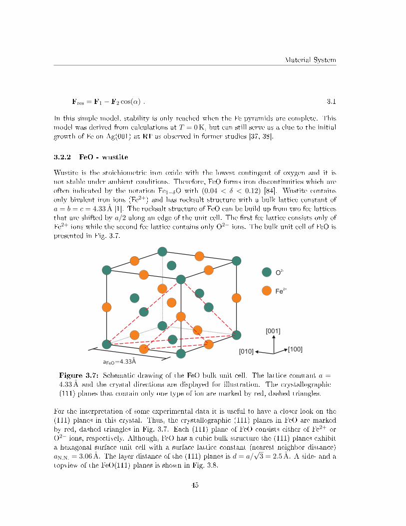
Material System
Fres = F1 − F2 cos(α) . 3.1
In this simple model, stability is only reached when the Fe pyramids are complete. Thismodel was derived from calculations at T = 0 K, but can still serve as a clue to the initialgrowth of Fe on Ag(001) at RT as observed in former studies [37, 38].
3.2.2 FeO - wustite
Wustite is the stoichiometric iron oxide with the lowest contingent of oxygen and it isnot stable under ambient conditions. Therefore, FeO forms iron discontinuities which areoften indicated by the notation Fe1−δO with (0.04 < δ < 0.12) [84]. Wustite containsonly bivalent iron ions (Fe2+) and has rocksalt structure with a bulk lattice constant ofa = b = c = 4.33 A [1]. The rocksalt structure of FeO can be build up from two fcc latticesthat are shifted by a/2 along an edge of the unit cell. The �rst fcc lattice consists only ofFe2+ ions while the second fcc lattice contains only O2− ions. The bulk unit cell of FeO ispresented in Fig. 3.7.
[001]
[100]
Fe2+
O2-
[010]
Figure 3.7: Schematic drawing of the FeO bulk unit cell. The lattice constant a =4.33 A and the crystal directions are displayed for illustration. The crystallographic(111) planes that contain only one type of ion are marked by red, dashed triangles.
For the interpretation of some experimental data it is useful to have a closer look on the(111) planes in this crystal. Thus, the crystallographic (111) planes in FeO are markedby red, dashed triangles in Fig. 3.7. Each (111) plane of FeO consists either of Fe2+ orO2− ions, respectively. Although, FeO has a cubic bulk structure the (111) planes exhibita hexagonal surface unit cell with a surface lattice constant (nearest neighbor distance)aN.N. = 3.06 A. The layer distance of the (111) planes is d = a/
√3 = 2.5 A. A side- and a
topview of the FeO(111) planes is shown in Fig. 3.8.
45
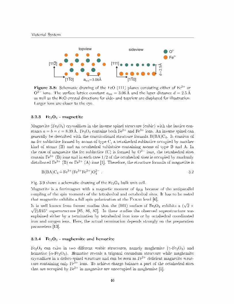
Material System
topview sideview
[1 0]1
[11 ]2
[1 0]1
[111]
O2-
Fe2+
aN.N.
Figure 3.8: Schematic drawing of the FeO (111) planes consisting either of Fe2+ orO2− ions. The surface lattice constant ann = 3.06 A and the layer distance d = 2.5 Aas well as the FeO crystal directions for side- and topview are displayed for illustration.Larger ions are closer to the eye.
3.2.3 Fe3O4 - magnetite
Magnetite (Fe3O4) crystallizes in the inverse spinel structure (cubic) with the lattice con-stants a = b = c = 8.39 A. Fe3O4 contains both Fe2+ and Fe3+ ions. An inverse spinel cangenerally be described with the constitutional structure formula B(BA)C4. It consists ofan fcc sublattice formed by atoms of type C, a tetrahedral sublattice occupied by anotherkind of atoms (B) and an octahedral sublattice containing atoms of type B and A. Inthe case of magnetite the fcc sublattice (C) is formed by O2− ions, the tetrahedral sitescontain Fe3+ (B) ions and in each case 1/2 of the octahedral sites is occupied by randomlydistributed Fe3+ (B) or Fe2+ (A) ions [1]. Therefore, the structure formula of magnetite is
B(BA)C4 = Fe3+(Fe3+Fe2+)O2−4 . 3.2
Fig. 3.9 shows a schematic drawing of the Fe3O4 bulk unit cell.
Magnetite is a ferrimagnet with a magnetic moment of 4µB because of the antiparallelcoupling of the spin moments of the tetrahedral and octahedral sites. It has to be notedthat magnetite exhibits a full spin polarization at the Fermi level [6].
It is well known from former studies that the (001) surface of Fe3O4 exhibits a (√
2 ×√2)R45◦ superstructure [85, 86, 87]. In these studies the observed superstructure was
explained either by a termination by tetrahedral iron ions or by octahedral coordinatediron and oxygen ions. Here, the actual termination depends strongly on the preparationparameters [13].
3.2.4 Fe2O3 - maghemite and hematite
Fe2O3 can exist in two di�erent stable structures, namely maghemite (γ-Fe2O3) andhematite (α-Fe2O3). Hematite reveals a trigonal corundum structure while maghemitecrystallizes in a defect-spinel structure and can be seen as Fe2+ de�cient magnetite struc-ture containing only Fe3+ ions. To achieve charge balance a part of the octahedral sitesthat are occupied by Fe2+ in magnetite are unoccupied in maghemite [1].
46
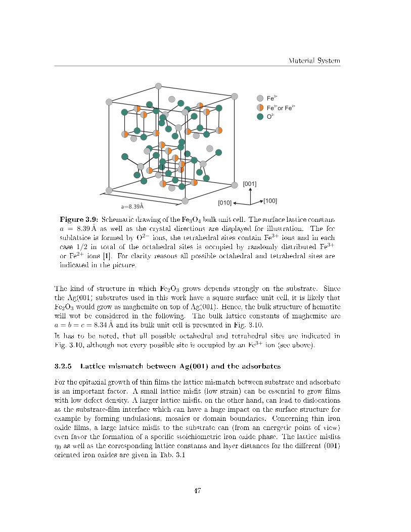
Material System
Fe3+
Fe3+
O2-
or Fe2+
[001]
[100][010]
Figure 3.9: Schematic drawing of the Fe3O4 bulk unit cell. The surface lattice constanta = 8.39 A as well as the crystal directions are displayed for illustration. The fccsublattice is formed by O2− ions, the tetrahedral sites contain Fe3+ ions and in eachcase 1/2 in total of the octahedral sites is occupied by randomly distributed Fe3+
or Fe2+ ions [1]. For clarity reasons all possible octahedral and tetrahedral sites areindicated in the picture.
The kind of structure in which Fe2O3 grows depends strongly on the substrate. Sincethe Ag(001) substrates used in this work have a square surface unit cell, it is likely thatFe2O3 would grow as maghemite on top of Ag(001). Hence, the bulk structure of hematitewill wot be considered in the following. The bulk lattice constants of maghemite area = b = c = 8.34 A and its bulk unit cell is presented in Fig. 3.10.
It has to be noted, that all possible octahedral and tetrahedral sites are indicated inFig. 3.10, although not every possible site is occupied by an Fe3+ ion (see above).
3.2.5 Lattice mismatch between Ag(001) and the adsorbates
For the epitaxial growth of thin �lms the lattice mismatch between substrate and adsorbateis an important factor. A small lattice mis�t (low strain) can be essential to grow �lmswith low defect density. A larger lattice mis�t, on the other hand, can lead to dislocationsat the substrate-�lm interface which can have a huge impact on the surface structure forexample by forming undulations, mosaics or domain boundaries. Concerning thin ironoxide �lms, a large lattice mis�t to the substrate can (from an energetic point of view)even favor the formation of a speci�c stoichiometric iron oxide phase. The lattice mis�tsη0 as well as the corresponding lattice constants and layer distances for the di�erent (001)oriented iron oxides are given in Tab. 3.1
47
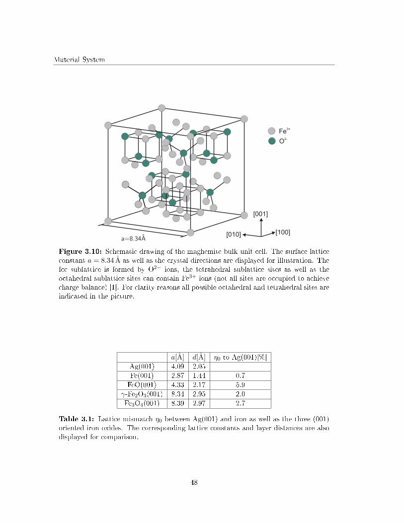
Material System
Fe3+
O2-
[001]
[100][010]
Figure 3.10: Schematic drawing of the maghemite bulk unit cell. The surface latticeconstant a = 8.34 A as well as the crystal directions are displayed for illustration. Thefcc sublattice is formed by O2− ions, the tetrahedral sublattice sites as well as theoctahedral sublattice sites can contain Fe3+ ions (not all sites are occupied to achievecharge balance) [1]. For clarity reasons all possible octahedral and tetrahedral sites areindicated in the picture.
a[A] d[A] η0 to Ag(001)[%]
Ag(001) 4.09 2.05 -
Fe(001) 2.87 1.44 0.7
FeO(001) 4.33 2.17 5.9
γ-Fe2O3(001) 8.34 2.95 2.0
Fe3O4(001) 8.39 2.97 2.7
Table 3.1: Lattice mismatch η0 between Ag(001) and iron as well as the three (001)oriented iron oxides. The corresponding lattice constants and layer distances are alsodisplayed for comparison.
48
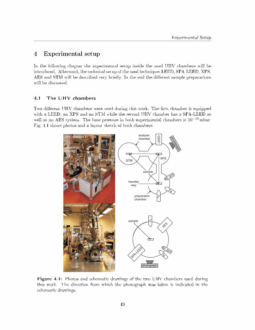
Experimental Setup
4 Experimental setup
In the following chapter the experimental setup inside the used UHV chambers will beintroduced. Afterward, the technical setup of the used techniques LEED, SPA-LEED, XPS,AES and STM will be described very brie�y. In the end the di�erent sample preparationswill be discussed.
4.1 The UHV chambers
Two di�erent UHV chambers were used during this work. The �rst chamber is equippedwith a LEED, an XPS and an STM while the second UHV chamber has a SPA-LEED aswell as an AES system. The base pressure in both experimental chambers is 10−10 mbar.Fig. 4.1 shows photos and a layout sketch of both chambers.
XPS
LEED
preparationchamber
STMLE
ED
Fe
sp. gun
sample
transferway
preparationchamber
analysischamber
XPSSTM
UHV chamber #1
UHV chamber #2
AES
evaporator
SPA-LEED
Fe
sp. gun
sample
AES
SPA
-LEED
photograph
photo
gra
ph
Figure 4.1: Photos and schematic drawings of the two UHV chambers used duringthis work. The direction from which the photograph was taken is indicated in theschematic drawings.
49
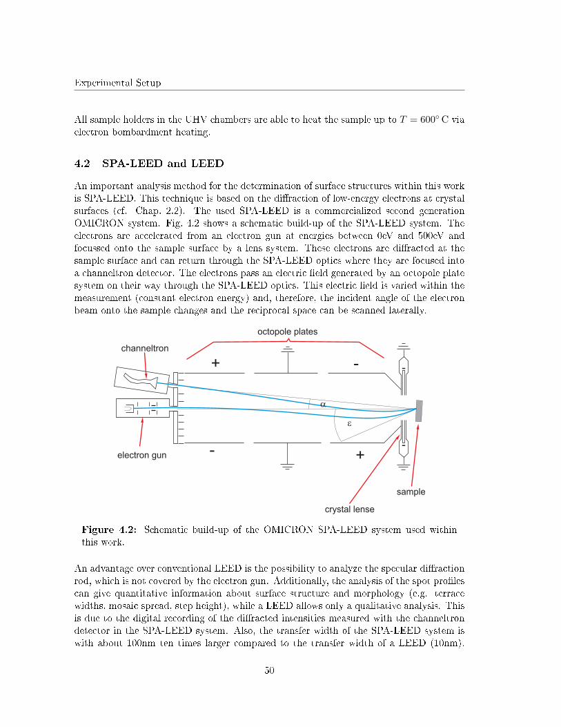
Experimental Setup
All sample holders in the UHV chambers are able to heat the sample up to T = 600◦C viaelectron bombardment heating.
4.2 SPA-LEED and LEED
An important analysis method for the determination of surface structures within this workis SPA-LEED. This technique is based on the di�raction of low-energy electrons at crystalsurfaces (cf. Chap. 2.2). The used SPA-LEED is a commercialized second generationOMICRON system. Fig. 4.2 shows a schematic build-up of the SPA-LEED system. Theelectrons are accelerated from an electron gun at energies between 0eV and 500eV andfocussed onto the sample surface by a lens system. These electrons are di�racted at thesample surface and can return through the SPA-LEED optics where they are focused intoa channeltron detector. The electrons pass an electric �eld generated by an octopole platesystem on their way through the SPA-LEED optics. This electric �eld is varied within themeasurement (constant electron energy) and, therefore, the incident angle of the electronbeam onto the sample changes and the reciprocal space can be scanned laterally.
crystal lense
channeltron
-
--
-+
+
e
sample
octopole plates
electron gun
a
Figure 4.2: Schematic build-up of the OMICRON SPA-LEED system used withinthis work.
An advantage over conventional LEED is the possibility to analyze the specular di�ractionrod, which is not covered by the electron gun. Additionally, the analysis of the spot pro�lescan give quantitative information about surface structure and morphology (e.g. terracewidths, mosaic spread, step height), while a LEED allows only a qualitative analysis. Thisis due to the digital recording of the di�racted intensities measured with the channeltrondetector in the SPA-LEED system. Also, the transfer width of the SPA-LEED system iswith about 100nm ten times larger compared to the transfer width of a LEED (10nm).
50
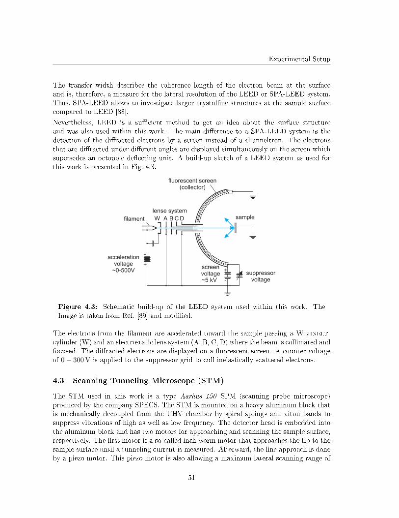
Experimental Setup
The transfer width describes the coherence length of the electron beam at the surfaceand is, therefore, a measure for the lateral resolution of the LEED or SPA-LEED system.Thus, SPA-LEED allows to investigate larger crystalline structures at the sample surfacecompared to LEED [88].
Nevertheless, LEED is a su�cient method to get an idea about the surface structureand was also used within this work. The main di�erence to a SPA-LEED system is thedetection of the di�racted electrons by a screen instead of a channeltron. The electronsthat are di�racted under di�erent angles are displayed simultaneously on the screen whichsupersedes an octopole de�ecting unit. A build-up sketch of a LEED system as used forthis work is presented in Fig. 4.3.
W A B C D
lense system
filament
accelerationvoltage
~0-500V suppressorvoltage
sample
fluorescent screen(collector)
~5 kV
-
-
+
+screenvoltage
Figure 4.3: Schematic build-up of the LEED system used within this work. TheImage is taken from Ref. [89] and modi�ed.
The electrons from the �lament are accelerated toward the sample passing a Wehnelt-cylinder (W) and an electrostatic lens system (A, B, C, D) where the beam is collimated andfocused. The di�racted electrons are displayed on a �uorescent screen. A counter voltageof 0− 300 V is applied to the suppressor grid to cull inelastically scattered electrons.
4.3 Scanning Tunneling Microscope (STM)
The STM used in this work is a type Aarhus 150 SPM (scanning probe microscope)produced by the company SPECS. The STM is mounted on a heavy aluminum block thatis mechanically decoupled from the UHV chamber by spiral springs and viton bands tosuppress vibrations of high as well as low frequency. The detector head is embedded intothe aluminum block and has two motors for approaching and scanning the sample surface,respectively. The �rst motor is a so-called inch-worm motor that approaches the tip to thesample surface until a tunneling current is measured. Afterward, the �ne approach is doneby a piezo motor. This piezo motor is also allowing a maximum lateral scanning range of
51
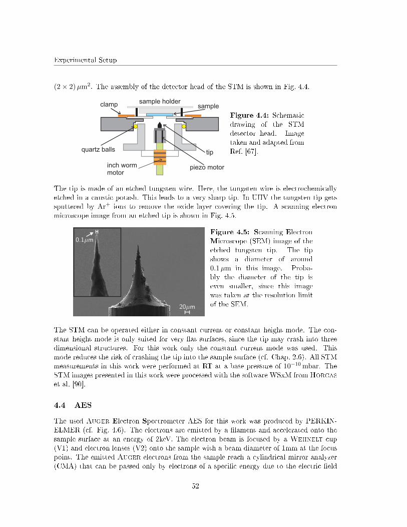
Experimental Setup
(2× 2)µm2. The assembly of the detector head of the STM is shown in Fig. 4.4.
inch wormmotor
piezo motor
sampleclamp sample holder
quartz balls
Figure 4.4: Schematicdrawing of the STMdetector head. Imagetaken and adapted fromRef. [67].
The tip is made of an etched tungsten wire. Here, the tungsten wire is electrochemicallyetched in a caustic potash. This leads to a very sharp tip. In UHV the tungsten tip getssputtered by Ar+ ions to remove the oxide layer covering the tip. A scanning electronmicroscope image from an etched tip is shown in Fig. 4.5.
Figure 4.5: Scanning ElectronMicroscope (SEM) image of theetched tungsten tip. The tipshows a diameter of around0.1µm in this image. Proba-bly the diameter of the tip iseven smaller, since this imagewas taken at the resolution limitof the SEM.
The STM can be operated either in constant current or constant height mode. The con-stant height mode is only suited for very �at surfaces, since the tip may crash into threedimensional structures. For this work only the constant current mode was used. Thismode reduces the risk of crashing the tip into the sample surface (cf. Chap. 2.6). All STMmeasurements in this work were performed at RT at a base pressure of 10−10 mbar. TheSTM images presented in this work were processed with the software WSxM from Horcas
et al. [90].
4.4 AES
The used Auger Electron Spectrometer AES for this work was produced by PERKIN-ELMER (cf. Fig. 4.6). The electrons are emitted by a �lament and accelerated onto thesample surface at an energy of 2keV. The electron beam is focused by a Wehnelt cup(V1) and electron lenses (V2) onto the sample with a beam diameter of 1mm at the focuspoint. The emitted Auger electrons from the sample reach a cylindrical mirror analyzer(CMA) that can be passed only by electrons of a speci�c energy due to the electric �eld
52
Experimental Setup
inside the CMA. The passed electrons are detected by an electron multiplier. The electric�eld inside the CMA is varied during an AES experiment so that an energy spectrum ofthe emitted electrons can be obtained.
samplefilament
V1
V2
electronmultiplier
CMAFigure 4.6: Schematicbuild-up of the AES opticsused in this work. Onlythe electrons that have the�tting kinetic energy canpass the CMA (dashed,green lines).
4.5 XPS
For chemical analysis of the sample surface also an XPS from SPECS was used. The X-raysource is of the type XR50 and the semi spherical analyzer is a PHOIBOS 150. The X-raysare emitted from an Al anode. Since the XPS has no monochromator the photoemissonspectra are mainly in�uenced by the most intense emission lines of the Al anode, whichis EK,α = 1486.6 eV. A schematic drawing of the X-ray source and the semi sphericalanalyzer is given in Fig. 4.7.
sample
X-raysource
channeltronslensesystem
e-
semi spherical analyzer
Figure 4.7: Two dimen-sional schematic build-upsketch of the SPECS XPSsystem used in this work.
The emitted photoelectrons are focused by lense system and enter a semi spherical analyzerafterward. Only photoelectrons with a speci�c energy can pass the analyzer and reach thechanneltrons. Therefore, by varying the electric �eld inside the semi spherical analyzer aspectrum of the emitted photoelectrons is obtained. The PHOIBOS 150 analyzer possessesa six channeltron array and during a measurement the signals of all six channels are addedup.
53
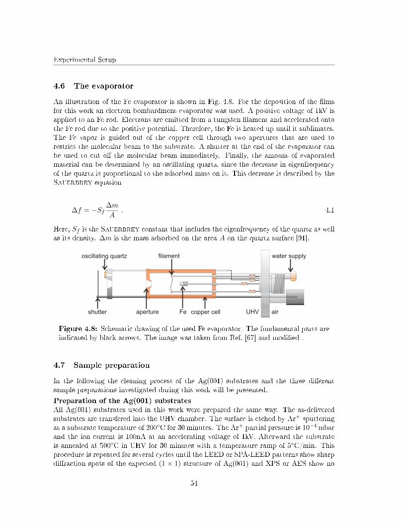
Experimental Setup
4.6 The evaporator
An illustration of the Fe evaporator is shown in Fig. 4.8. For the deposition of the �lmsfor this work an electron bombardment evaporator was used. A positive voltage of 1kV isapplied to an Fe rod. Electrons are emitted from a tungsten �lament and accelerated ontothe Fe rod due to the positive potential. Therefore, the Fe is heated up until it sublimates.The Fe vapor is guided out of the copper cell through two apertures that are used torestrict the molecular beam to the substrate. A shutter at the end of the evaporator canbe used to cut o� the molecular beam immediately. Finally, the amount of evaporatedmaterial can be determined by an oscillating quartz, since the decrease in eigenfrequencyof the quartz is proportional to the adsorbed mass on it. This decrease is described by theSauerbrey equation
∆f = −Sf∆m
A. 4.1
Here, Sf is the Sauerbrey constant that includes the eigenfrequency of the quartz as wellas its density. ∆m is the mass adsorbed on the area A on the quartz surface [91].
Fe UHVshutter
oscillating quartz filament
air
water supply
aperture copper cell
Figure 4.8: Schematic drawing of the used Fe evaporator. The fundamental parts areindicated by black arrows. The image was taken from Ref. [67] and modi�ed .
4.7 Sample preparation
In the following the cleaning process of the Ag(001) substrates and the three di�erentsample preparations investigated during this work will be presented.
Preparation of the Ag(001) substrates
All Ag(001) substrates used in this work were prepared the same way. The as-deliveredsubstrates are transfered into the UHV chamber. The surface is etched by Ar+ sputteringat a substrate temperature of 200◦C for 30 minutes. The Ar+ partial pressure is 10−4 mbarand the ion current is 100nA at an accelerating voltage of 1kV. Afterward the substrateis annealed at 500◦C in UHV for 30 minutes with a temperature ramp of 5◦C/min. Thisprocedure is repeated for several cycles until the LEED or SPA-LEED patterns show sharpdi�raction spots of the expected (1 × 1) structure of Ag(001) and XPS or AES show no
54
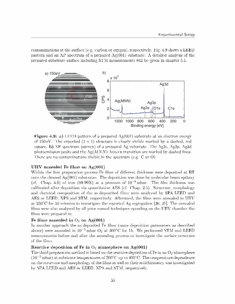
Experimental Setup
contaminations at the surface (e.g. carbon or oxygen), respectively. Fig. 4.9 shows a LEEDpattern and an XP spectrum of a prepared Ag(001) substrate. A detailed analysis of theprepared substrate surface including STM measurements will be given in chapter 5.1.
a) 150eV
Ag3d
Ag3pAg( )MNN
Ag3s
(01) (11)
Ag[1 0]1
Ag[110]
O1s C1s
(10)
b)
Figure 4.9: a) LEED pattern of a prepared Ag(001) substrate at an electron energyof 150 eV. The expected (1 × 1) structure is clearly visible marked by a dashed, redsquare. b) XP spectrum (survey) of a prepared Ag substrate. The Ag3s, Ag3p, Ag3dphotoemission peaks and the Ag(MNN) Auger transition are marked by dashed lines.There are no contaminations visible in the spectrum (e.g. C or O).
UHV annealed Fe �lms on Ag(001)
Within the �rst preparation process Fe �lms of di�erent thickness were deposited at RTonto the cleaned Ag(001) substrates. The deposition was done by molecular beam epitaxy(cf. Chap. 4.6) of iron (99.99%) at a pressure of 10−8 mbar. The �lm thickness wascalibrated after deposition via quantitative AES (cf. Chap. 2.5). Structure, morphologyand chemical composition of the as-depostited �lms were analyzed by SPA-LEED andAES or LEED, XPS and STM, respectively. Afterward, the �lms were annealed in UHVat 250◦C for 50 minutes to investigate the reported Ag segregation [30, 31]. The annealed�lms were also analyzed by all prior named techniques epending on the UHV chamber the�lms were prepared in.
Fe �lms annealed in O2 on Ag(001)
In another approach the as-deposited Fe �lms (same deposition parameters as describedabove) were annealed in 10−5 mbar O2 at 300◦C for 1h. We performed STM and LEEDmeasurements before and after the annealing process to investigate the surface structureof the �lms.
Reactive deposition of Fe in O2 atmosphere on Ag(001)
The third preparation method is based on the reactive deposition of Fe in an O2 atmosphere(10−5 mbar) at substrate temperatures of 200◦C up to 400◦C. The temperature dependenceon the structure and morphology of the �lms as well as their stoichiometry was investigatedby SPA-LEED and AES or LEED, XPS and STM, respectively.
55

Experimental Setup
56
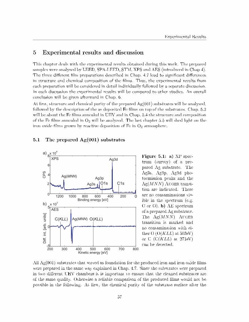
Experimental Results
5 Experimental results and discussion
This chapter deals with the experimental results obtained during this work. The preparedsamples were analyzed by LEED, SPA-LEED, STM, XPS and AES (introduced in Chap 4).The three di�erent �lm preparations described in Chap. 4.7 lead to signi�cant di�erencesin structure and chemical composition of the �lms. Thus, the experimental results fromeach preparation will be considered in detail individually followed by a separate discussion.In each discussion the experimental results will be compared to other studies. An overallconclusion will be given afterward in Chap. 6.
At �rst, structure and chemical purity of the prepared Ag(001) substrates will be analyzed,followed by the description of the as deposited Fe �lms on top of the substrates. Chap. 5.3will be about the Fe �lms annealed in UHV and in Chap. 5.4 the structure and compositionof the Fe �lms annealed in O2 will be analyzed. The last chapter 5.5 will shed light on theiron oxide �lms grown by reactive deposition of Fe in O2 atmosphere.
5.1 The prepared Ag(001) substrates
3
Diff. int. [arb
. units]
Ag3d
Ag3pAg( )MNN
Ag3s
Ag( )MNN
XPS
AES
O1s C1s
C( )KLL O( )KLL
a)
b)
Figure 5.1: a) XP spec-trum (survey) of a pre-pared Ag substrate. TheAg3s, Ag3p, Ag3d pho-toemission peaks and theAg(MNN) Auger transi-tion are indicated. Thereare no contaminations vis-ible in the spectrum (e.g.C or O). b) AE spectrumof a prepared Ag substrate.The Ag(MNN) Auger
transition is marked andno contamination with ei-ther O (O(KLL) at 503eV)or C (C(KLL) at 271eV)can be detected.
All Ag(001) substrates that served as foundation for the produced iron and iron oxide �lmswere prepared in the same way explained in Chap. 4.7. Since the substrates were preparedin two di�erent UHV chambers it is important to ensure that the cleaned substrates areof the same quality. Otherwise a reliable comparison of the produced �lms would not bepossible in the following. At �rst, the chemical purity of the substrate surface after the
57
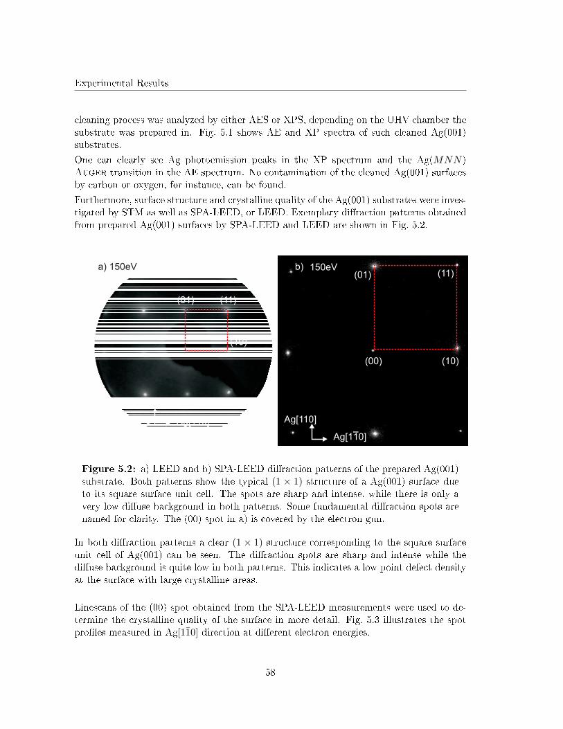
Experimental Results
cleaning process was analyzed by either AES or XPS, depending on the UHV chamber thesubstrate was prepared in. Fig. 5.1 shows AE and XP spectra of such cleaned Ag(001)substrates.
One can clearly see Ag photoemission peaks in the XP spectrum and the Ag(MNN)Auger transition in the AE spectrum. No contamination of the cleaned Ag(001) surfacesby carbon or oxygen, for instance, can be found.
Furthermore, surface structure and crystalline quality of the Ag(001) substrates were inves-tigated by STM as well as SPA-LEED, or LEED. Exemplary di�raction patterns obtainedfrom prepared Ag(001) surfaces by SPA-LEED and LEED are shown in Fig. 5.2.
(00) (10)
150eVb)a) 150eV
(01) (11)
Ag[1 0]1
Ag[110]
(10)
(01) (11)
Ag[1 0]1
Ag[110]
Figure 5.2: a) LEED and b) SPA-LEED di�raction patterns of the prepared Ag(001)substrate. Both patterns show the typical (1 × 1) structure of a Ag(001) surface dueto its square surface unit cell. The spots are sharp and intense, while there is only avery low di�use background in both patterns. Some fundamental di�raction spots arenamed for clarity. The (00) spot in a) is covered by the electron gun.
In both di�raction patterns a clear (1 × 1) structure corresponding to the square surfaceunit cell of Ag(001) can be seen. The di�raction spots are sharp and intense while thedi�use background is quite low in both patterns. This indicates a low point defect densityat the surface with large crystalline areas.
Linescans of the (00) spot obtained from the SPA-LEED measurements were used to de-termine the crystalline quality of the surface in more detail. Fig. 5.3 illustrates the spotpro�les measured in Ag[110] direction at di�erent electron energies.
58
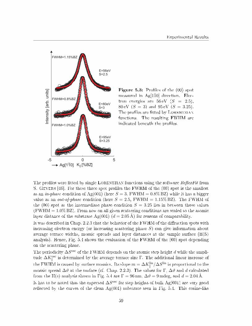
Experimental Results
E=56eVS=2.5
E=80eVS=3
E=95eVS=3.25
Inte
nsity [arb
. units]
K|| [%BZ]
FWHM=1.15%BZ
FWHM=0.8%BZ
FWHM=1.0%BZ
Ag[1 0]1
Figure 5.3: Pro�les of the (00) spotmeasured in Ag[110] direction. Elec-tron energies are 56 eV (S = 2.5),80 eV (S = 3) and 95 eV (S = 3.25).The pro�les are �tted by Lorentzianfunctions. The resulting FWHM areindicated beneath the pro�les.
The pro�les were �tted by single Lorentzian functions using the software Re�exFit fromS. Gevers [46]. For these three spot pro�les the FWHM of the (00) spot is the smallestat an in-phase condition of Ag(001) (here S = 3, FWHM = 0.8% BZ) while it has a biggervalue at an out-of-phase condition (here S = 2.5, FWHM = 1.15% BZ). The FWHM ofthe (00) spot at the intermediate phase condition S = 3.25 lies in between those values(FWHM = 1.0% BZ). From now on all given scattering conditions are scaled to the atomiclayer distance of the substrate Ag(001) (d = 2.05 A) for reasons of comparability.
It was described in Chap. 2.2.3 that the behavior of the FWHM of the di�raction spots withincreasing electron energy (or increasing scattering phase S) can give information aboutaverage terrace widths, mosaic spreads and layer distances at the sample surface (H(S)analysis). Hence, Fig. 5.4 shows the evaluation of the FWHM of the (00) spot dependingon the scattering phase.
The periodicity ∆Sosc of the FWHM depends on the atomic step height d while the ampli-tude ∆Kosc
‖ is determined by the average terrace size Γ. The additional linear increase of
the FWHM is caused by surface mosaics. Its slope m = ∆K lin‖ /∆S
lin is proportional to the
mosaic spread ∆ϑ at the surface (cf. Chap. 2.2.3). The values for Γ, ∆ϑ and d calculatedfrom the H(s) analysis shown in Fig. 5.4 are Γ = 96 nm, ∆ϑ = 9 mdeg, and d = 2.04 A.
It has to be noted that the expected ∆Sosc for step heights of bulk Ag(001) are very goodre�ected by the curves of the clean Ag(001) substrate seen in Fig. 5.4. This cosine-like
59
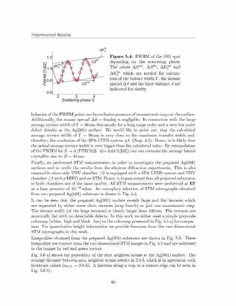
Experimental Results
DK ||
lin
lin
DS
DK ||
osc
42
osc
3Scattering phase S
1.0
0.8
1.2
0.6
DS
Figure 5.4: FWHM of the (00) spotdepending on the scattering phase.The values ∆Sosc, ∆Slin, ∆Kosc
|| and
∆Klin|| which are needed for calcula-
tion of the terrace width Γ, the mosaicspread ∆ϑ and the layer distance d areindicated for clarity.
behavior of the FWHM points to the exclusive presence of monoatomic steps at the surface.Additionally, the mosaic spread ∆ϑ = 9 mdeg is negligible. In connection with the largeaverage terrace width of Γ = 96 nm this speaks for a long range order and a very low pointdefect density at the Ag(001) surface. We would like to point out, that the calculatedaverage terrace width of Γ = 96 nm is very close to the maximum transfer width and,therefore, the resolution of the SPA-LEED system (cf. Chap. 4.2). Hence, it is likely thatthe actual average terrace width is even bigger than the calculated value. By extrapolationof the FWHM for S → 0 (FHWM(S=0)= 0.64 %[BZ]) one can estimate the average lateralcrystallite size to D = 45 nm.
Finally, we performed STM measurements in order to investigate the prepared Ag(001)surfaces and to verify the results from the electron di�raction experiments. This is alsoreasonable since only UHV chamber #2 is equipped with a SPA-LEED system and UHVchamber #1 with a LEED and an STM. Hence, it is guaranteed that all prepared substratesin both chambers are of the same quality. All STM measurements were performed at RTat a base pressure of 10−10 mbar. An exemplary selection of STM micrographs obtainedfrom one prepared Ag(001) substrate is shown in Fig. 5.5.
It can be seen that the prepared Ag(001) surface reveals large and �at terraces whichare separated by either some short terraces (step bunch) or just one monoatomic step.The terrace width (of the large terraces) is clearly larger than 100 nm. The terraces areatomically �at with no detectable defects. In this work we either used a simple greyscalecolormap (white=high and black=low) or the colormap presented in Fig. 5.5 a) for compar-ison. For quantitative height information we provide linescans from the two dimensionalSTM micrographs in this work.
Linepro�les obtained from the prepared Ag(001) substrate are shown in Fig. 5.6. Theselinepro�les are cutouts from the two dimensional STM images in Fig. 5.5 and are indicatedin the images by red and green arrows.
Fig. 5.6 a) shows the periodicity of the next neighbor atoms at the Ag(001) surface. Theaverage distance between next neighbor atoms results in 2.9 A which is in agreement withliterature values (aN.N. = 2.9 A). A linescan along a step at a terrace edge can be seen inFig. 5.6 b).
60
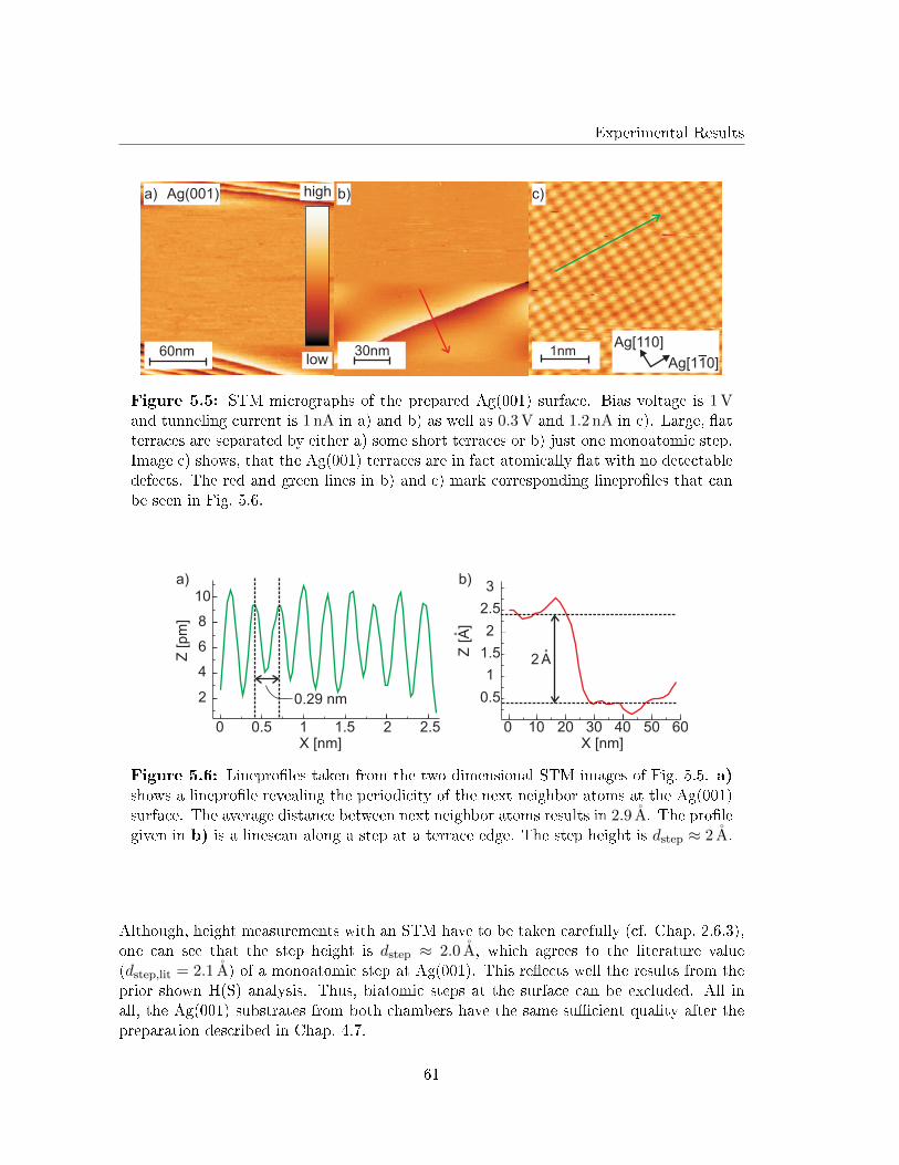
Experimental Results
60nm 30nm 1nmAg[1 0]1
Ag[110]
a) Ag(001) b) c)high
low
Figure 5.5: STM micrographs of the prepared Ag(001) surface. Bias voltage is 1 Vand tunneling current is 1 nA in a) and b) as well as 0.3 V and 1.2 nA in c). Large, �atterraces are separated by either a) some short terraces or b) just one monoatomic step.Image c) shows, that the Ag(001) terraces are in fact atomically �at with no detectabledefects. The red and green lines in b) and c) mark corresponding linepro�les that canbe seen in Fig. 5.6.
6050403020100
3
2.5
2
1.5
1
0.5
X [nm]
Z[A
]
10
8
6
4
2
X [nm]
Z [
pm
]
0 1 20.5 1.5 2.5
0.29 nm
2 A
a) b)
Figure 5.6: Linepro�les taken from the two dimensional STM images of Fig. 5.5. a)shows a linepro�le revealing the periodicity of the next neighbor atoms at the Ag(001)surface. The average distance between next neighbor atoms results in 2.9 A. The pro�legiven in b) is a linescan along a step at a terrace edge. The step height is dstep ≈ 2 A.
Although, height measurements with an STM have to be taken carefully (cf. Chap. 2.6.3),one can see that the step height is dstep ≈ 2.0 A, which agrees to the literature value(dstep,lit = 2.1 A) of a monoatomic step at Ag(001). This re�ects well the results from theprior shown H(S) analysis. Thus, biatomic steps at the surface can be excluded. All inall, the Ag(001) substrates from both chambers have the same su�cient quality after thepreparation described in Chap. 4.7.
61
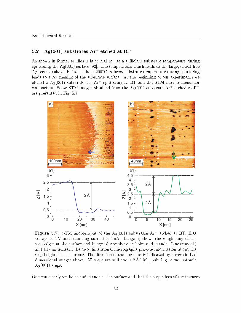
Experimental Results
5.2 Ag(001) substrates Ar+ etched at RT
As shown in former studies it is crucial to use a su�cient substrate temperature duringsputtering the Ag(001) surface [92]. The temperature which leads to the large, defect freeAg terraces shown before is about 200◦C. A lower substrate temperature during sputteringleads to a roughening of the substrate surface. At the beginning of our experiments weetched a Ag(001) substrate via Ar+ sputtering at RT and did STM measurements forcomparison. Some STM images obtained from the Ag(001) substrate Ar+ etched at RTare presented in Fig. 5.7.
2520151050
4.54
3.53
2.52
1.51
0.50
X [nm]
Z[ Å
]
403020100
3
2.5
2
1.5
1
0.5
0
X [nm]
Z[ Å
]
2 A
2 A
2 A
a) b)
100nm 40nm
a1) b1)
Figure 5.7: STM micrographs of the Ag(001) substratre Ar+ etched at RT. Biasvoltage is 1 V and tunneling current is 1 nA. Image a) shows the roughening of thestep edges at the surface and image b) reveals some holes and islands. Linescans a1)and b1) underneath the two dimensional micrographs provide information about thestep heights at the surface. The direction of the linescans is indicated by arrows in twodimensional images above. All steps are still about 2 A high, pointing to monoatomicAg(001) steps.
One can clearly see holes and islands at the surface and that the step edges of the terraces
62
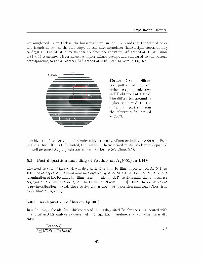
Experimental Results
are roughened. Nevertheless, the linescans shown in Fig. 5.7 proof that the formed holesand islands as well as the step edges do still have monolayer (ML) height correspondingto Ag(001). The LEED patterns obtained from the substrate Ar+ etched at RT still showa (1 × 1) structure. Nevertheless, a higher di�use background compared to the patterncorresponding to the substrates Ar+ etched at 200◦C can be seen in Fig. 5.8.
150eV
(01) (11)
Ag[1 0]1
Ag[110]
(10)
Figure 5.8: Di�rac-tion pattern of the Ar+
etched Ag(001) substrateat RT obtained at 150 eV.The di�use background ishigher compared to thedi�raction pattern fromthe substrates Ar+ etchedat 200◦C.
The higher di�use background indicates a higher density of non periodically ordered defectsat the surface. It has to be noted, that all �lms characterized in this work were depositedon well prepared Ag(001) substrates as shown before (cf. Chap. 5.1).
5.3 Post deposition annealing of Fe �lms on Ag(001) in UHV
The next section of this work will deal with ultra thin Fe �lms deposited on Ag(001) atRT. The as-deposited Fe �lms were investigated by AES, SPA-LEED and STM. After theexamination of the Fe �lms, the �lms were annealed in UHV to determine the reported Agsegregation and its dependency on the Fe �lm thickness [30, 31]. This Chapter serves asa pre-investigation towards the reactive grown and post deposition annealed (PDA) ironoxide �lms on Ag(001).
5.3.1 As deposited Fe �lms on Ag(001)
In a �rst step, the absolute thicknesses of the as-deposited Fe �lms were calibrated withquantitative AES analysis as described in Chap. 2.5. Therefore, the normalized intensityratio
Fe(LMM)
Ag(MNN) + Fe(LMM)5.1
63
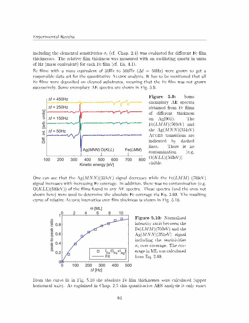
Experimental Results
including the elemental sensitivities σi (cf. Chap. 2.4) was evaluated for di�erent Fe �lmthicknesses. The relative �lm thickness was measured with an oscillating quartz in unitsof Hz (mass equivalent) for each Fe �lm (cf. Eq. 4.1).
Fe �lms with a mass equivalent of 50Hz to 500Hz (∆f = 50Hz) were grown to get aresponsible data set for the quantitative Auger analysis. It has to be mentioned that allFe �lms were deposited on cleaned substrates, meaning that the Fe �lm was not grownsuccessively. Some exemplary AE spectra are shown in Fig. 5.9.
Fe( )LMMAg( )MNN
Df = 450Hz
Df = 250Hz
Df = 150Hz
Df = 50Hz
Diff. int. [arb
. units]
O( )KLL
Figure 5.9: Someexemplary AE spectraobtained from Fe �lmsof di�erent thicknesson Ag(001). TheFe(LMM)(703eV) andthe Ag(MNN)(351eV)Auger transitions areindicated by dashedlines. There is nocontamination (e.g.O(KLL)(503eV))visible.
One can see that the Ag(MNN)(351eV) signal decreases while the Fe(LMM) (703eV)signal increases with increasing Fe coverage. In addition, there was no contamination (e.g.O(KLL)(503eV)) of the �lms found in any AE spectra. These spectra (and the ones notshown here) were used to determine the absolute Fe coverage via Eq. 2.69. The resultingcurve of relative Auger intensities over �lm thickness is shown in Fig. 5.10.
2 4 6 8 10Q [ML]
Df [Hz]
peak-t
o-p
eak r
atio Figure 5.10: Normalized
intensity ratio between theFe(LMM)(703eV) and theAg(MNN)(351eV) signalincluding the sensitivitiesσi over coverage. The cov-erage in ML was calculatedfrom Eq. 2.69.
From the curve �t in Fig. 5.10 the absolute Fe �lm thicknesses were calculated (upperhorizontal axis). As explained in Chap. 2.5 this quantitative AES analysis is only exact
64
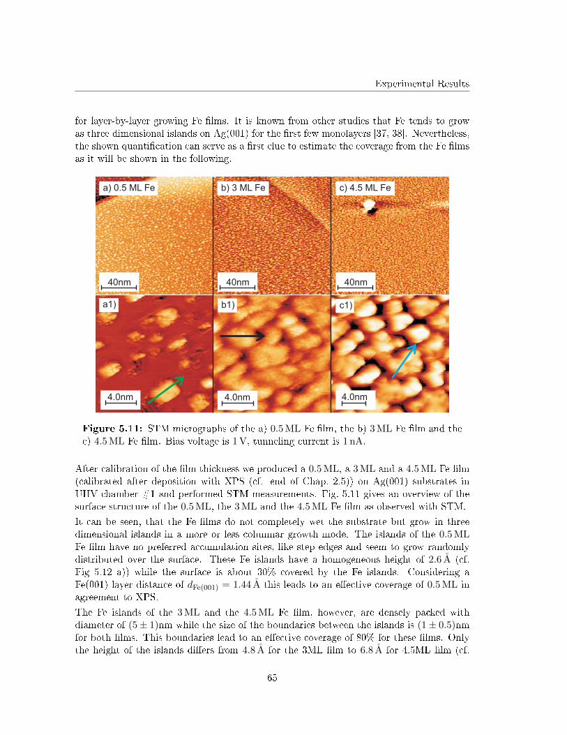
Experimental Results
for layer-by-layer growing Fe �lms. It is known from other studies that Fe tends to growas three dimensional islands on Ag(001) for the �rst few monolayers [37, 38]. Nevertheless,the shown quanti�cation can serve as a �rst clue to estimate the coverage from the Fe �lmsas it will be shown in the following.
4.0nm 4.0nm
40nm40nm40nm
4.0nm
a) 0.5 ML Fe b) 3 ML Fe
a1) b1)
c) 4.5 ML Fe
c1)
Figure 5.11: STM micrographs of the a) 0.5 ML Fe �lm, the b) 3 ML Fe �lm and thec) 4.5 ML Fe �lm. Bias voltage is 1 V, tunneling current is 1 nA.
After calibration of the �lm thickness we produced a 0.5 ML, a 3 ML and a 4.5 ML Fe �lm(calibrated after deposition with XPS (cf. end of Chap. 2.5)) on Ag(001) substrates inUHV chamber #1 and performed STM measurements. Fig. 5.11 gives an overview of thesurface structure of the 0.5 ML, the 3 ML and the 4.5 ML Fe �lm as observed with STM.
It can be seen, that the Fe �lms do not completely wet the substrate but grow in threedimensional islands in a more or less columnar growth mode. The islands of the 0.5 MLFe �lm have no preferred accumulation sites, like step edges and seem to grow randomlydistributed over the surface. These Fe islands have a homogeneous height of 2.6 A (cf.Fig 5.12 a)) while the surface is about 30% covered by the Fe islands. Considering aFe(001) layer distance of dFe(001) = 1.44 A this leads to an e�ective coverage of 0.5 ML inagreement to XPS.
The Fe islands of the 3 ML and the 4.5 ML Fe �lm, however, are densely packed withdiameter of (5± 1)nm while the size of the boundaries between the islands is (1± 0.5)nmfor both �lms. This boundaries lead to an e�ective coverage of 80% for these �lms. Onlythe height of the islands di�ers from 4.8 A for the 3ML �lm to 6.8 A for 4.5ML �lm (cf.
65
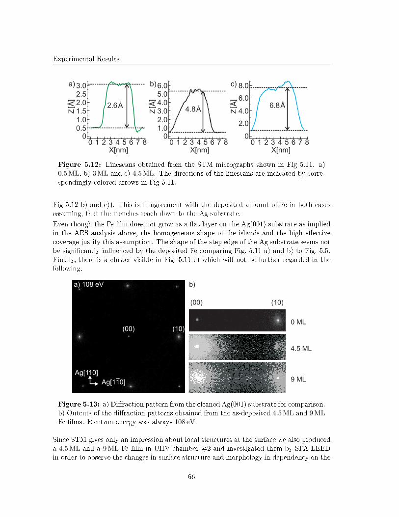
Experimental Results
876543210
3.02.52.01.51.00.5
0
X[nm]
Z[ Å
]
2.6Å
876543210
8.0
4.0
0
X[nm]
Z[ Å
]
6.8Å6.0
2.0
876543210X[nm]
Z[ Å
]
4.8Å
6.05.04.03.02.01.0
0
a) b) c)
Figure 5.12: Linescans obtained from the STM micrographs shown in Fig 5.11. a)0.5 ML, b) 3 ML and c) 4.5 ML. The directions of the linescans are indicated by corre-spondingly colored arrows in Fig 5.11.
Fig 5.12 b) and c)). This is in agreement with the deposited amount of Fe in both casesassuming, that the trenches reach down to the Ag substrate.
Even though the Fe �lm does not grow as a �at layer on the Ag(001) substrate as impliedin the AES analysis above, the homogeneous shape of the islands and the high e�ectivecoverage justify this assumption. The shape of the step edge of the Ag substrate seems notbe signi�cantly in�uenced by the deposited Fe comparing Fig. 5.11 a) and b) to Fig. 5.5.Finally, there is a cluster visible in Fig. 5.11 c) which will not be further regarded in thefollowing.
(00) (10)
(00) (10)
a) 108 eV b)
0 ML
4.5 ML
9 MLAg[1 0]1
Ag[110]
Figure 5.13: a) Di�raction pattern from the cleaned Ag(001) substrate for comparison.b) Outcuts of the di�raction patterns obtained from the as-deposited 4.5 ML and 9 MLFe �lms. Electron energy was always 108 eV.
Since STM gives only an impression about local structures at the surface we also produceda 4.5 ML and a 9 ML Fe �lm in UHV chamber #2 and investigated them by SPA-LEEDin order to observe the changes in surface structure and morphology in dependency on the
66
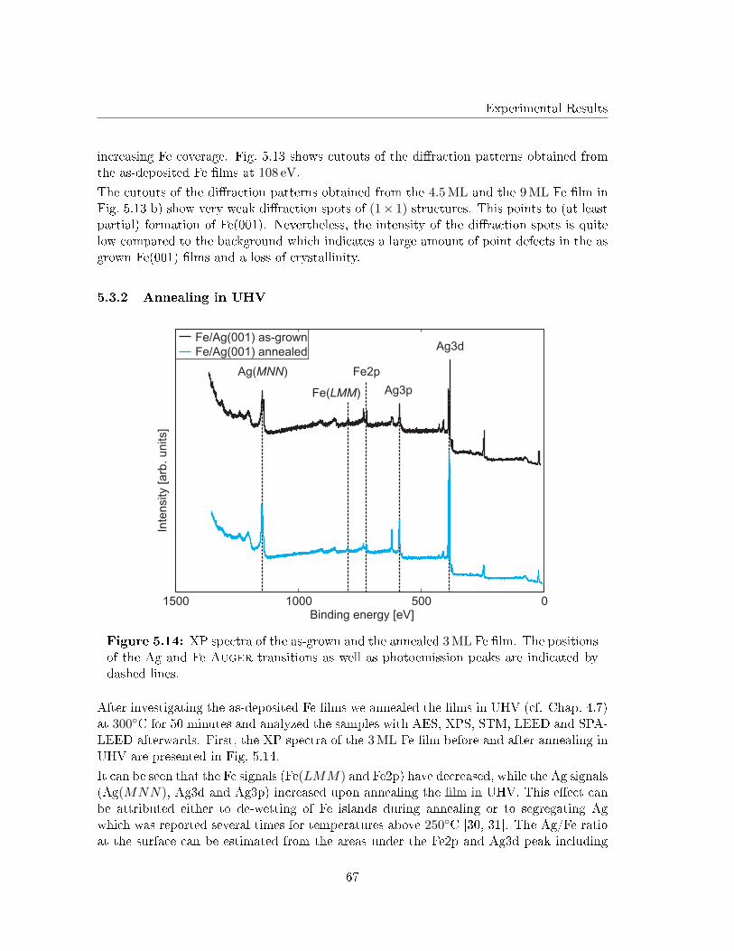
Experimental Results
increasing Fe coverage. Fig. 5.13 shows cutouts of the di�raction patterns obtained fromthe as-deposited Fe �lms at 108 eV.
The cutouts of the di�raction patterns obtained from the 4.5 ML and the 9 ML Fe �lm inFig. 5.13 b) show very weak di�raction spots of (1× 1) structures. This points to (at leastpartial) formation of Fe(001). Nevertheless, the intensity of the di�raction spots is quitelow compared to the background which indicates a large amount of point defects in the asgrown Fe(001) �lms and a loss of crystallinity.
5.3.2 Annealing in UHV
Ag3d
Ag3p
Ag( )MNN Fe2p
Fe( )LMM
050010001500Binding energy [eV]
Inte
nsity [arb
. units]
Fe/Ag(001) as-grown
Fe/Ag(001) annealed
Figure 5.14: XP spectra of the as-grown and the annealed 3 ML Fe �lm. The positionsof the Ag and Fe Auger transitions as well as photoemission peaks are indicated bydashed lines.
After investigating the as-deposited Fe �lms we annealed the �lms in UHV (cf. Chap. 4.7)at 300◦C for 50 minutes and analyzed the samples with AES, XPS, STM, LEED and SPA-LEED afterwards. First, the XP spectra of the 3 ML Fe �lm before and after annealing inUHV are presented in Fig. 5.14.
It can be seen that the Fe signals (Fe(LMM) and Fe2p) have decreased, while the Ag signals(Ag(MNN), Ag3d and Ag3p) increased upon annealing the �lm in UHV. This e�ect canbe attributed either to de-wetting of Fe islands during annealing or to segregating Agwhich was reported several times for temperatures above 250◦C [30, 31]. The Ag/Fe ratioat the surface can be estimated from the areas under the Fe2p and Ag3d peak including
67
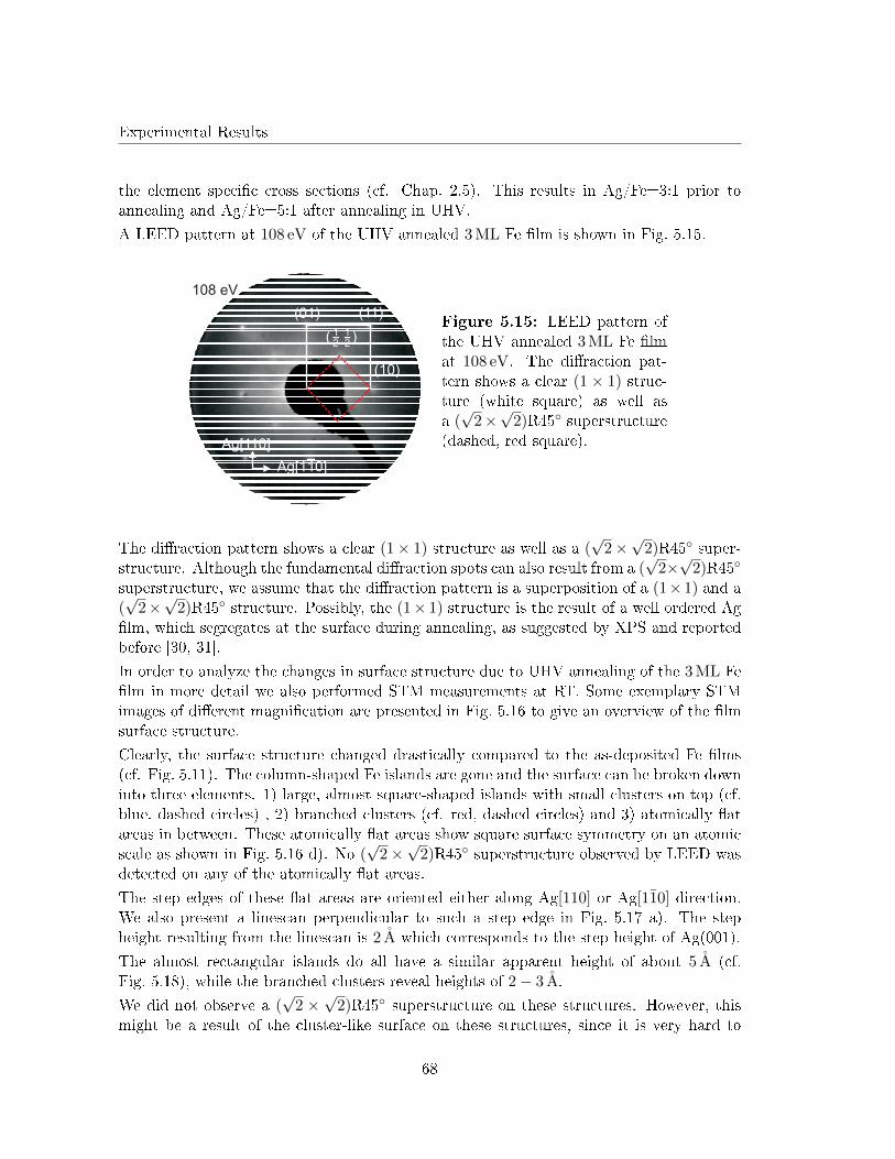
Experimental Results
the element speci�c cross sections (cf. Chap. 2.5). This results in Ag/Fe=3:1 prior toannealing and Ag/Fe=5:1 after annealing in UHV.
A LEED pattern at 108 eV of the UHV annealed 3 ML Fe �lm is shown in Fig. 5.15.
108 eV
Ag[1 0]1
Ag[110]
(10)
(01) (11)
( 12
12)
Figure 5.15: LEED pattern ofthe UHV annealed 3 ML Fe �lmat 108 eV. The di�raction pat-tern shows a clear (1 × 1) struc-ture (white square) as well asa (√
2×√
2)R45◦ superstructure(dashed, red square).
The di�raction pattern shows a clear (1× 1) structure as well as a (√
2×√
2)R45◦ super-structure. Although the fundamental di�raction spots can also result from a (
√2×√
2)R45◦
superstructure, we assume that the di�raction pattern is a superposition of a (1×1) and a(√
2×√
2)R45◦ structure. Possibly, the (1× 1) structure is the result of a well ordered Ag�lm, which segregates at the surface during annealing, as suggested by XPS and reportedbefore [30, 31].
In order to analyze the changes in surface structure due to UHV annealing of the 3 ML Fe�lm in more detail we also performed STM measurements at RT. Some exemplary STMimages of di�erent magni�cation are presented in Fig. 5.16 to give an overview of the �lmsurface structure.
Clearly, the surface structure changed drastically compared to the as-deposited Fe �lms(cf. Fig. 5.11). The column-shaped Fe islands are gone and the surface can be broken downinto three elements. 1) large, almost square-shaped islands with small clusters on top (cf.blue, dashed circles) , 2) branched clusters (cf. red, dashed circles) and 3) atomically �atareas in between. These atomically �at areas show square surface symmetry on an atomicscale as shown in Fig. 5.16 d). No (
√2×√
2)R45◦ superstructure observed by LEED wasdetected on any of the atomically �at areas.
The step edges of these �at areas are oriented either along Ag[110] or Ag[110] direction.We also present a linescan perpendicular to such a step edge in Fig. 5.17 a). The stepheight resulting from the linescan is 2 A which corresponds to the step height of Ag(001).
The almost rectangular islands do all have a similar apparent height of about 5 A (cf.Fig. 5.18), while the branched clusters reveal heights of 2− 3 A.
We did not observe a (√
2 ×√
2)R45◦ superstructure on these structures. However, thismight be a result of the cluster-like surface on these structures, since it is very hard to
68
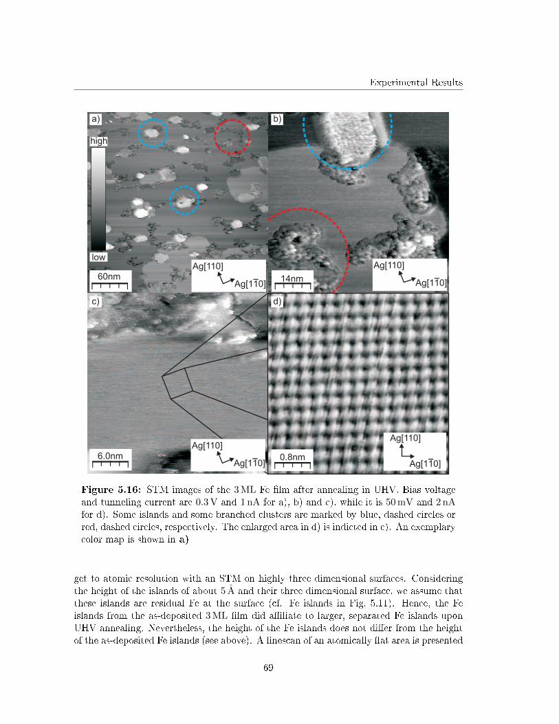
Experimental Results
6.0nm 0.8nmAg[1 0]1
Ag[110]
Ag[1 0]1
Ag[110]
Ag[1 0]1
Ag[110]
Ag[1 0]1
Ag[110]
60nm 14nm
a) b)
c) d)
low
high
Figure 5.16: STM images of the 3 ML Fe �lm after annealing in UHV. Bias voltageand tunneling current are 0.3 V and 1 nA for a), b) and c), while it is 50 mV and 2 nAfor d). Some islands and some branched clusters are marked by blue, dashed circles orred, dashed circles, respectively. The enlarged area in d) is indicted in c). An exemplarycolor map is shown in a)
get to atomic resolution with an STM on highly three dimensional surfaces. Consideringthe height of the islands of about 5 A and their three dimensional surface, we assume thatthese islands are residual Fe at the surface (cf. Fe islands in Fig. 5.11). Hence, the Feislands from the as-deposited 3 ML �lm did a�liate to larger, separated Fe islands uponUHV annealing. Nevertheless, the height of the Fe islands does not di�er from the heightof the as-deposited Fe islands (see above). A linescan of an atomically �at area is presented
69
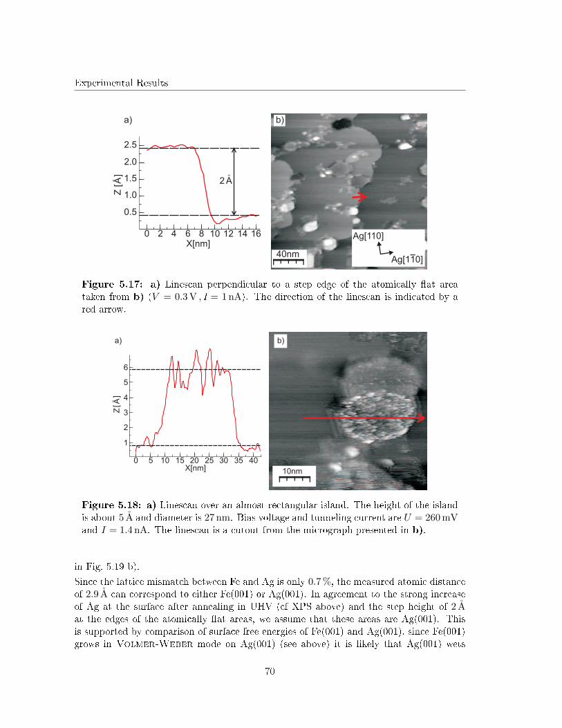
Experimental Results
1614121086420
2.5
2.0
1.5
1.0
0.5
X[nm]
Z[Å
]
2 A
a)
Ag[1 0]1
Ag[110]
40nm
b)
Figure 5.17: a) Linescan perpendicular to a step edge of the atomically �at areataken from b) (V = 0.3 V , I = 1 nA). The direction of the linescan is indicated by ared arrow.
10nm
4035302520151050
6
5
4
3
2
1
X[nm]
Z[ Å
]
b)a)
Figure 5.18: a) Linescan over an almost rectangular island. The height of the islandis about 5 A and diameter is 27 nm. Bias voltage and tunneling current are U = 260 mVand I = 1.4 nA. The linescan is a cutout from the micrograph presented in b).
in Fig. 5.19 b).
Since the lattice mismatch between Fe and Ag is only 0.7 %, the measured atomic distanceof 2.9 A can correspond to either Fe(001) or Ag(001). In agreement to the strong increaseof Ag at the surface after annealing in UHV (cf XPS above) and the step height of 2 Aat the edges of the atomically �at areas, we assume that these areas are Ag(001). Thisis supported by comparison of surface free energies of Fe(001) and Ag(001), since Fe(001)grows in Volmer-Weber mode on Ag(001) (see above) it is likely that Ag(001) wets
70
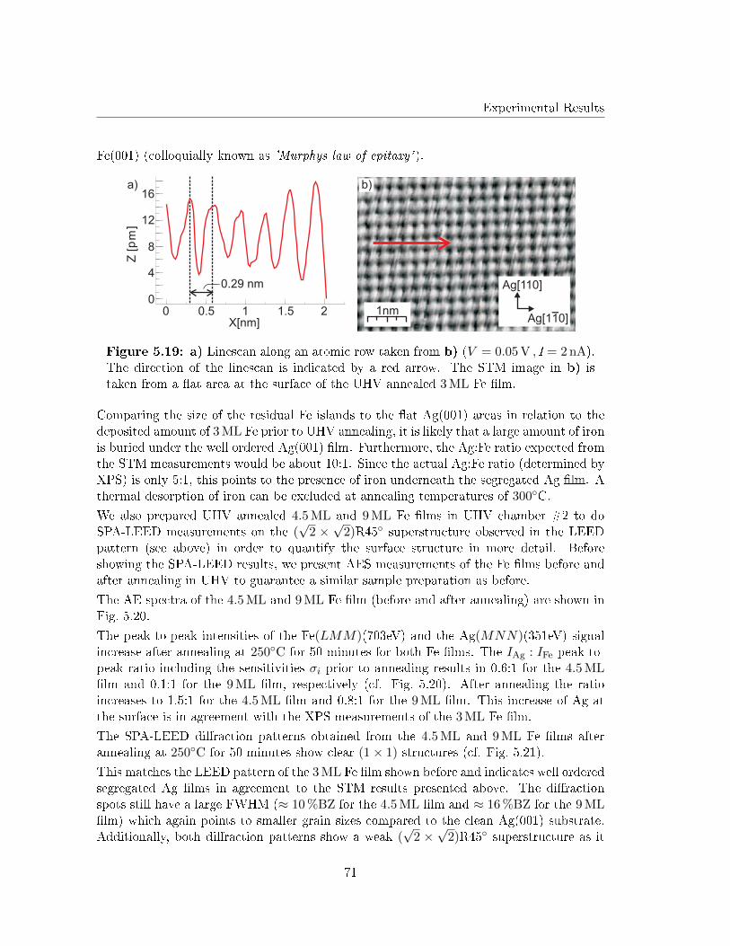
Experimental Results
Fe(001) (colloquially known as 'Murphys law of epitaxy' ).
0.29 nm
X[nm]
Z[p
m]
21.510.50
16
12
8
4
0
a)
1nmAg[1 0]1
Ag[110]
b)
Figure 5.19: a) Linescan along an atomic row taken from b) (V = 0.05 V , I = 2 nA).The direction of the linescan is indicated by a red arrow. The STM image in b) istaken from a �at area at the surface of the UHV annealed 3 ML Fe �lm.
Comparing the size of the residual Fe islands to the �at Ag(001) areas in relation to thedeposited amount of 3 ML Fe prior to UHV annealing, it is likely that a large amount of ironis buried under the well ordered Ag(001) �lm. Furthermore, the Ag:Fe ratio expected fromthe STM measurements would be about 10:1. Since the actual Ag:Fe ratio (determined byXPS) is only 5:1, this points to the presence of iron underneath the segregated Ag �lm. Athermal desorption of iron can be excluded at annealing temperatures of 300◦C.
We also prepared UHV annealed 4.5 ML and 9 ML Fe �lms in UHV chamber #2 to doSPA-LEED measurements on the (
√2 ×√
2)R45◦ superstructure observed in the LEEDpattern (see above) in order to quantify the surface structure in more detail. Beforeshowing the SPA-LEED results, we present AES measurements of the Fe �lms before andafter annealing in UHV to guarantee a similar sample preparation as before.
The AE spectra of the 4.5 ML and 9 ML Fe �lm (before and after annealing) are shown inFig. 5.20.
The peak-to-peak intensities of the Fe(LMM)(703eV) and the Ag(MNN)(351eV) signalincrease after annealing at 250◦C for 50 minutes for both Fe �lms. The IAg : IFe peak-to-peak ratio including the sensitivities σi prior to annealing results in 0.6:1 for the 4.5 ML�lm and 0.1:1 for the 9 ML �lm, respectively (cf. Fig. 5.20). After annealing the ratioincreases to 1.5:1 for the 4.5 ML �lm and 0.8:1 for the 9 ML �lm. This increase of Ag atthe surface is in agreement with the XPS measurements of the 3 ML Fe �lm.
The SPA-LEED di�raction patterns obtained from the 4.5 ML and 9 ML Fe �lms afterannealing at 250◦C for 50 minutes show clear (1× 1) structures (cf. Fig. 5.21).
This matches the LEED pattern of the 3 ML Fe �lm shown before and indicates well orderedsegregated Ag �lms in agreement to the STM results presented above. The di�ractionspots still have a large FWHM (≈ 10 %BZ for the 4.5 ML �lm and ≈ 16 %BZ for the 9 ML�lm) which again points to smaller grain sizes compared to the clean Ag(001) substrate.Additionally, both di�raction patterns show a weak (
√2 ×√
2)R45◦ superstructure as it
71
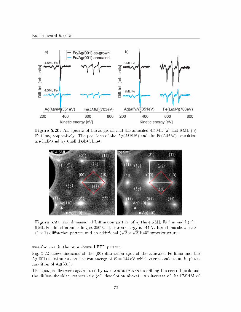
Experimental ResultsD
iff.
in
t. [
arb
. u
nits]
Kinetic energy [eV]
200 400 600 800
a) b)Fe/Ag(001) as-grown
Fe/Ag(001) annealed
4.5ML Fe 9ML Fe
Ag( )(351eV)MNN Fe( )(703eV)LMM
Diff.
in
t. [
arb
. u
nits]
Kinetic energy [eV]
200 400 600 800
4.5ML Fe 9ML Fe
Fe/Ag(001) as-grown
Fe/Ag(001) annealed
Ag( )(351eV)MNN Fe( )(703eV)LMM
Figure 5.20: AE spectra of the as-grown and the annealed 4.5 ML (a) and 9 ML (b)Fe �lms, respectively. The positions of the Ag(MNN) and the Fe(LMM) transitionare indicated by small dashed lines.
(01) (11)
(00) (10)
(11)(01)(11)
(11) ( )12
12( )1
212
( )12
12
( )12
12
(01) (11)
(00) (10)
(11)(01)(11)
(10)
(11) ( )12
12( )1
212
( )12
12( )1
212
a) 4.5ML b) 9ML
Ag[1 0]1
Ag[110]
Ag[1 0]1
Ag[110]
Figure 5.21: two dimensional Di�raction pattern of a) the 4.5 ML Fe �lm and b) the9 ML Fe �lm after annealing at 250◦C. Electron energy is 144eV. Both �lms show clear(1× 1) di�raction pattern and an additional (
√2×√
2)R45◦ superstructure.
was also seen in the prior shown LEED pattern.
Fig. 5.22 shows linescans of the (00) di�raction spot of the annealed Fe �lms and theAg(001) substrate at an electron energy of E = 144 eV which corresponds to an in-phasecondition of Ag(001).
The spot pro�les were again �tted by two Lorentzians describing the central peak andthe di�use shoulder, respectively (cf. description above). An increase of the FWHM of
72
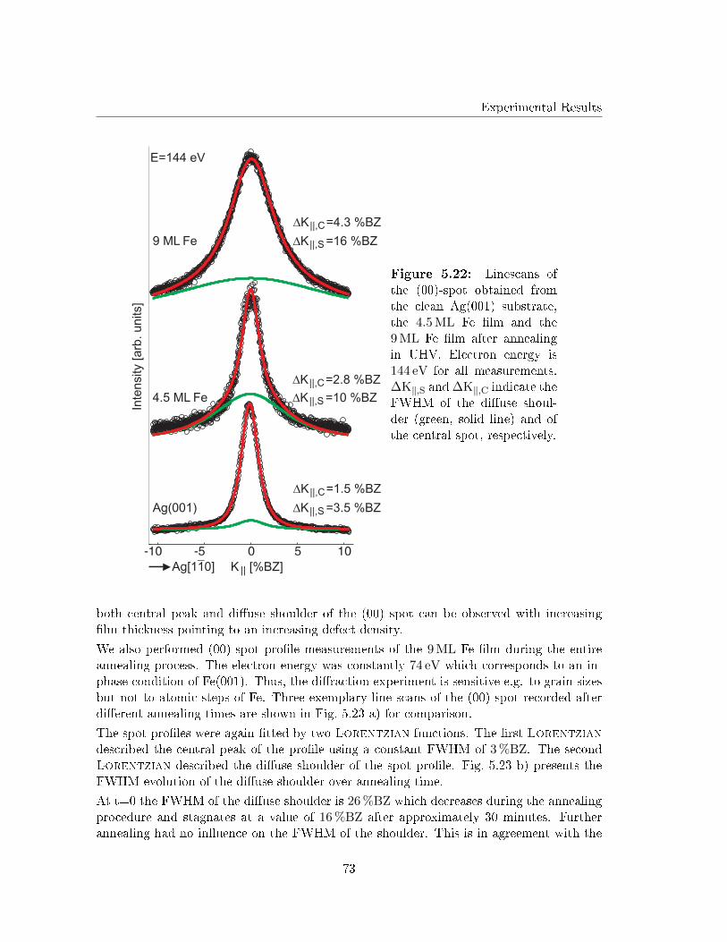
Experimental Results
Inte
nsity [
arb
. u
nits]
Ag(001)
4.5 ML Fe
9 ML Fe DK =16 %BZ||,S
DK =10 %BZ||,S
DK =3.5 %BZ||,S
K [%BZ]||Ag[1 0]1
E=144 eV
DK =4.3 %BZ||,C
DK =2.8 %BZ||,C
D ||,C
Figure 5.22: Linescans ofthe (00)-spot obtained fromthe clean Ag(001) substrate,the 4.5 ML Fe �lm and the9 ML Fe �lm after annealingin UHV. Electron energy is144 eV for all measurements.∆K‖,S and ∆K‖,C indicate theFWHM of the di�use shoul-der (green, solid line) and ofthe central spot, respectively.
both central peak and di�use shoulder of the (00) spot can be observed with increasing�lm thickness pointing to an increasing defect density.
We also performed (00)-spot pro�le measurements of the 9 ML Fe �lm during the entireannealing process. The electron energy was constantly 74 eV which corresponds to an in-phase condition of Fe(001). Thus, the di�raction experiment is sensitive e.g. to grain sizesbut not to atomic steps of Fe. Three exemplary line scans of the (00) spot recorded afterdi�erent annealing times are shown in Fig. 5.23 a) for comparison.
The spot pro�les were again �tted by two Lorentzian functions. The �rst Lorentziandescribed the central peak of the pro�le using a constant FWHM of 3 %BZ. The secondLorentzian described the di�use shoulder of the spot pro�le. Fig. 5.23 b) presents theFWHM evolution of the di�use shoulder over annealing time.
At t=0 the FWHM of the di�use shoulder is 26 %BZ which decreases during the annealingprocedure and stagnates at a value of 16 %BZ after approximately 30 minutes. Furtherannealing had no in�uence on the FWHM of the shoulder. This is in agreement with the
73
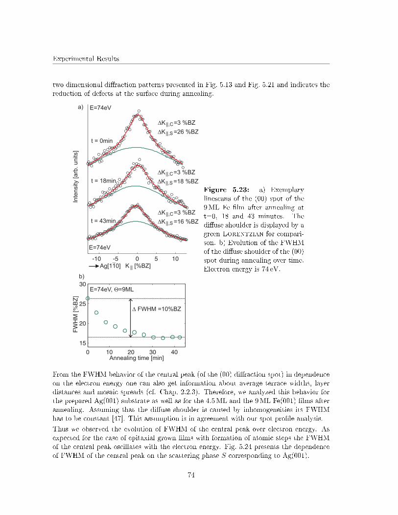
Experimental Results
two dimensional di�raction patterns presented in Fig. 5.13 and Fig. 5.21 and indicates thereduction of defects at the surface during annealing.
D FWHM =10%BZ
E=74eV, =9MLQ
b)
Inte
nsity [arb
. units]
t = 0min
t = 18min
t = 43min
K [%BZ]||Ag[1 0]1
E=74eV
a)
Annealing time [min]
E=74eV
DK =26 %BZ||,S
DK =3 %BZ||,C
DK =18 %BZ||,S
DK =3 %BZ||,C
DK =16 %BZ||,S
DK =3 %BZ||,C
Figure 5.23: a) Exemplarylinescans of the (00) spot of the9 ML Fe �lm after annealing att=0, 18 and 43 minutes. Thedi�use shoulder is displayed by agreen Lorentzian for compari-son. b) Evolution of the FWHMof the di�use shoulder of the (00)spot during annealing over time.Electron energy is 74 eV.
From the FWHM behavior of the central peak (of the (00) di�raction spot) in dependenceon the electron energy one can also get information about average terrace widths, layerdistances and mosaic spreads (cf. Chap. 2.2.3). Therefore, we analyzed this behavior forthe prepared Ag(001) substrate as well as for the 4.5 ML and the 9 ML Fe(001) �lms afterannealing. Assuming that the di�use shoulder is caused by inhomogeneities its FWHMhas to be constant [47]. This assumption is in agreement with our spot pro�le analysis.
Thus we observed the evolution of FWHM of the central peak over electron energy. Asexpected for the case of epitaxial grown �lms with formation of atomic steps the FWHMof the central peak oscillates with the electron energy. Fig. 5.24 presents the dependenceof FWHM of the central peak on the scattering phase S corresponding to Ag(001).
74
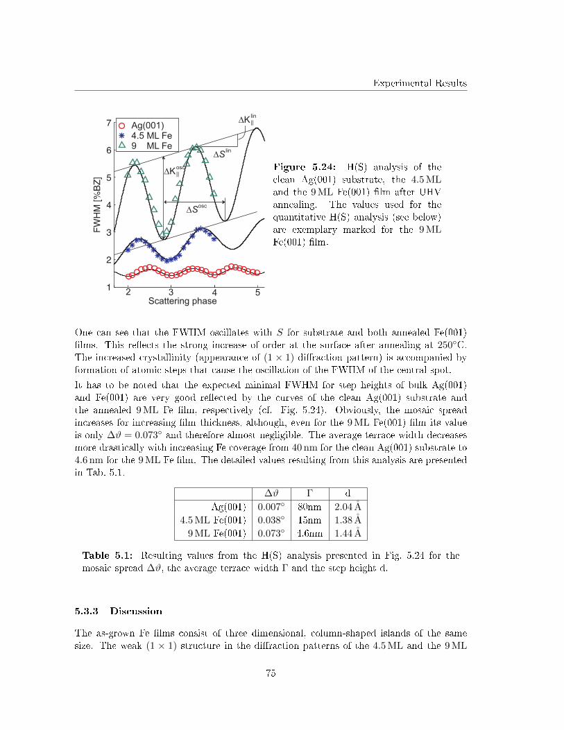
Experimental Results
Ag(001)4.5 ML Fe9 ML Fe
DK ||
lin
DSlin
DS
DK ||
osc
42
osc
3 5Scattering phase
Figure 5.24: H(S) analysis of theclean Ag(001) substrate, the 4.5 MLand the 9 ML Fe(001) �lm after UHVannealing. The values used for thequantitative H(S) analysis (see below)are exemplary marked for the 9 MLFe(001) �lm.
One can see that the FWHM oscillates with S for substrate and both annealed Fe(001)�lms. This re�ects the strong increase of order at the surface after annealing at 250◦C.The increased crystallinity (appearance of (1 × 1) di�raction pattern) is accompanied byformation of atomic steps that cause the oscillation of the FWHM of the central spot.
It has to be noted that the expected minimal FWHM for step heights of bulk Ag(001)and Fe(001) are very good re�ected by the curves of the clean Ag(001) substrate andthe annealed 9 ML Fe �lm, respectively (cf. Fig. 5.24). Obviously, the mosaic spreadincreases for increasing �lm thickness, although, even for the 9 ML Fe(001) �lm its valueis only ∆ϑ = 0.073◦ and therefore almost negligible. The average terrace width decreasesmore drastically with increasing Fe coverage from 40 nm for the clean Ag(001) substrate to4.6 nm for the 9 ML Fe �lm. The detailed values resulting from this analysis are presentedin Tab. 5.1.
∆ϑ Γ d
Ag(001) 0.007◦ 80nm 2.04 A
4.5 ML Fe(001) 0.038◦ 15nm 1.38 A
9 ML Fe(001) 0.073◦ 4.6nm 1.44 A
Table 5.1: Resulting values from the H(S) analysis presented in Fig. 5.24 for themosaic spread ∆ϑ, the average terrace width Γ and the step height d.
5.3.3 Discussion
The as-grown Fe �lms consist of three dimensional, column-shaped islands of the samesize. The weak (1 × 1) structure in the di�raction patterns of the 4.5 ML and the 9 ML
75
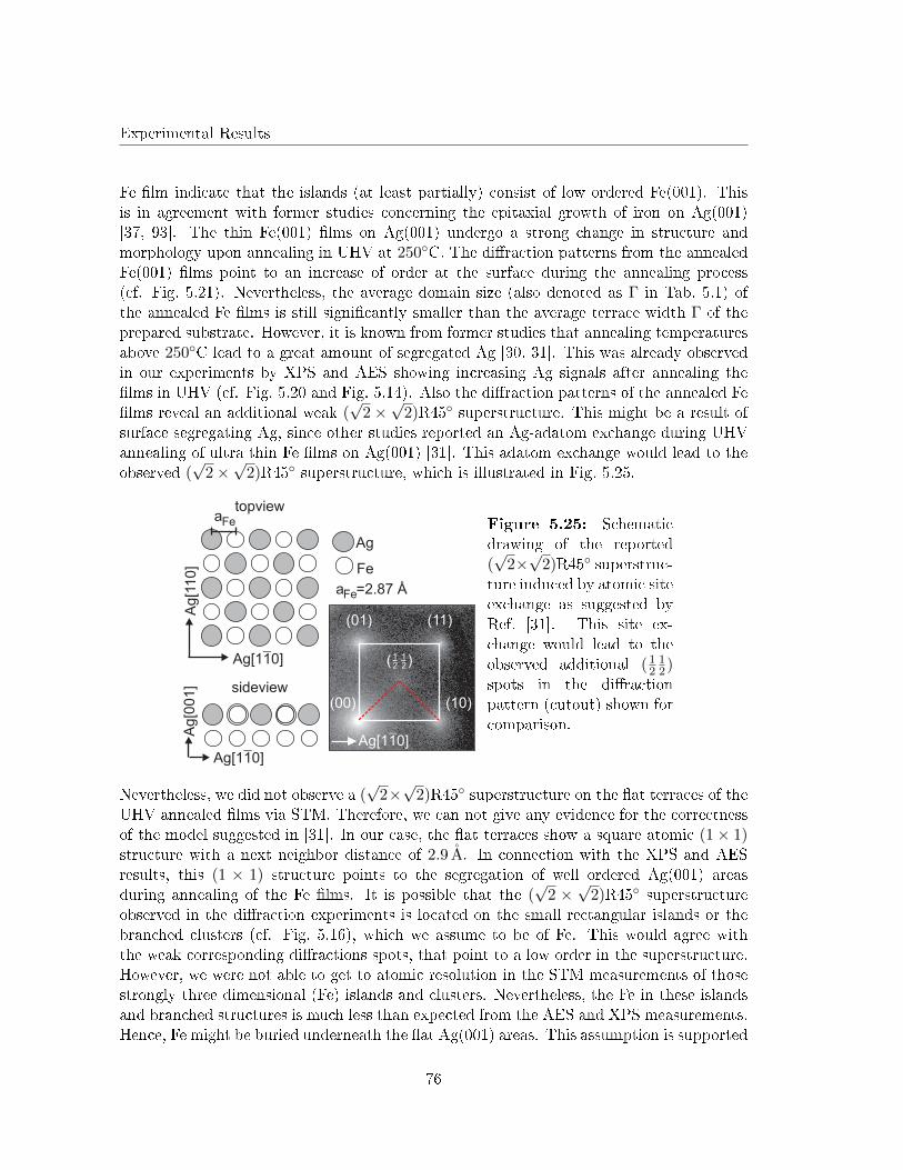
Experimental Results
Fe �lm indicate that the islands (at least partially) consist of low ordered Fe(001). Thisis in agreement with former studies concerning the epitaxial growth of iron on Ag(001)[37, 93]. The thin Fe(001) �lms on Ag(001) undergo a strong change in structure andmorphology upon annealing in UHV at 250◦C. The di�raction patterns from the annealedFe(001) �lms point to an increase of order at the surface during the annealing process(cf. Fig. 5.21). Nevertheless, the average domain size (also denoted as Γ in Tab. 5.1) ofthe annealed Fe �lms is still signi�cantly smaller than the average terrace width Γ of theprepared substrate. However, it is known from former studies that annealing temperaturesabove 250◦C lead to a great amount of segregated Ag [30, 31]. This was already observedin our experiments by XPS and AES showing increasing Ag signals after annealing the�lms in UHV (cf. Fig. 5.20 and Fig. 5.14). Also the di�raction patterns of the annealed Fe�lms reveal an additional weak (
√2×√
2)R45◦ superstructure. This might be a result ofsurface segregating Ag, since other studies reported an Ag-adatom exchange during UHVannealing of ultra thin Fe �lms on Ag(001) [31]. This adatom exchange would lead to theobserved (
√2×√
2)R45◦ superstructure, which is illustrated in Fig. 5.25.
a =2.87 ÅFe
Ag
Fe
aFe
Ag[1 0]1
Ag[1
10]
Ag[1 0]1
Ag[0
01]
(01) (11)
( )12
12
(10)
Ag[1 0]1
(00)
topview
sideview
Figure 5.25: Schematicdrawing of the reported(√
2×√
2)R45◦ superstruc-ture induced by atomic siteexchange as suggested byRef. [31]. This site ex-change would lead to theobserved additional (1
212)
spots in the di�ractionpattern (cutout) shown forcomparison.
Nevertheless, we did not observe a (√
2×√
2)R45◦ superstructure on the �at terraces of theUHV annealed �lms via STM. Therefore, we can not give any evidence for the correctnessof the model suggested in [31]. In our case, the �at terraces show a square atomic (1× 1)structure with a next neighbor distance of 2.9 A. In connection with the XPS and AESresults, this (1 × 1) structure points to the segregation of well ordered Ag(001) areasduring annealing of the Fe �lms. It is possible that the (
√2 ×√
2)R45◦ superstructureobserved in the di�raction experiments is located on the small rectangular islands or thebranched clusters (cf. Fig. 5.16), which we assume to be of Fe. This would agree withthe weak corresponding di�ractions spots, that point to a low order in the superstructure.However, we were not able to get to atomic resolution in the STM measurements of thosestrongly three dimensional (Fe) islands and clusters. Nevertheless, the Fe in these islandsand branched structures is much less than expected from the AES and XPS measurements.Hence, Fe might be buried underneath the �at Ag(001) areas. This assumption is supported
76

Experimental Results
by the lower free energy of an Ag(001)/Fe(001) interface compared to the the free energyof the Fe(001) surface (cf. Fig. 3.6). Thus, a buried Fe �lm between a Ag(001) substrateand a segregated Ag(001) �lm would be energetically favorable. It is therefore questionablewhether the former reported Ag segregation at the Fe surface can rather be described asa Fe di�usion into the Ag substrate. We would like to note, that the (
√2 ×√
2)R45◦
superstructure observed in the di�raction patterns has not been reported in connection tothe segregation of Ag on UHV annealed Fe �lms on Ag(001) before.
77

Experimental Results
78
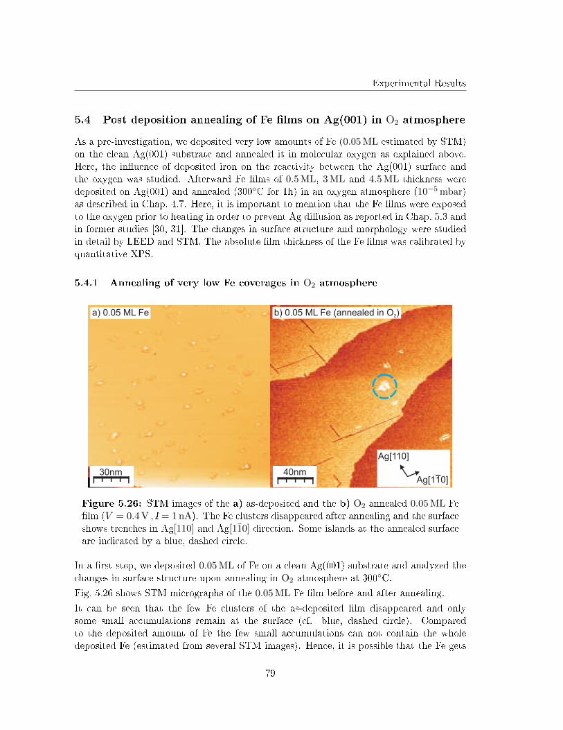
Experimental Results
5.4 Post deposition annealing of Fe �lms on Ag(001) in O2 atmosphere
As a pre-investigation, we deposited very low amounts of Fe (0.05 ML estimated by STM)on the clean Ag(001) substrate and annealed it in molecular oxygen as explained above.Here, the in�uence of deposited iron on the reactivity between the Ag(001) surface andthe oxygen was studied. Afterward Fe �lms of 0.5 ML, 3 ML and 4.5 ML thickness weredeposited on Ag(001) and annealed (300◦C for 1h) in an oxygen atmosphere (10−5 mbar)as described in Chap. 4.7. Here, it is important to mention that the Fe �lms were exposedto the oxygen prior to heating in order to prevent Ag di�usion as reported in Chap. 5.3 andin former studies [30, 31]. The changes in surface structure and morphology were studiedin detail by LEED and STM. The absolute �lm thickness of the Fe �lms was calibrated byquantitative XPS.
5.4.1 Annealing of very low Fe coverages in O2 atmosphere
30nm 40nm
a) 0.05 ML Fe b) 0.05 ML Fe (annealed in O )2
Ag[1 0]1
Ag[110]
Figure 5.26: STM images of the a) as-deposited and the b) O2 annealed 0.05 ML Fe�lm (V = 0.4 V , I = 1 nA). The Fe clusters disappeared after annealing and the surfaceshows trenches in Ag[110] and Ag[110] direction. Some islands at the annealed surfaceare indicated by a blue, dashed circle.
In a �rst step, we deposited 0.05 ML of Fe on a clean Ag(001) substrate and analyzed thechanges in surface structure upon annealing in O2 atmosphere at 300◦C.
Fig. 5.26 shows STM micrographs of the 0.05 ML Fe �lm before and after annealing.
It can be seen that the few Fe clusters of the as-deposited �lm disappeared and onlysome small accumulations remain at the surface (cf. blue, dashed circle). Comparedto the deposited amount of Fe the few small accumulations can not contain the wholedeposited Fe (estimated from several STM images). Hence, it is possible that the Fe gets
79
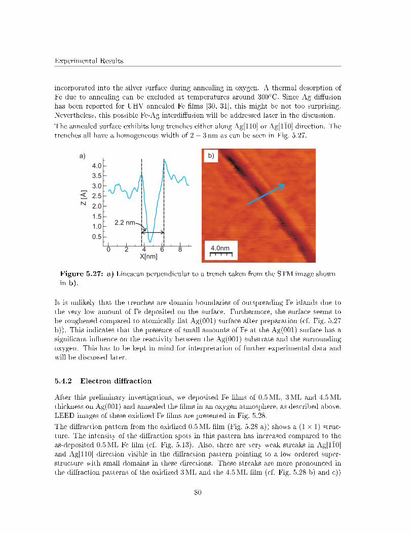
Experimental Results
incorporated into the silver surface during annealing in oxygen. A thermal desorption ofFe due to annealing can be excluded at temperatures around 300◦C. Since Ag di�usionhas been reported for UHV annealed Fe �lms [30, 31], this might be not too surprising.Nevertheless, this possible Fe-Ag interdi�usion will be addressed later in the discussion.
The annealed surface exhibits long trenches either along Ag[110] or Ag[110] direction. Thetrenches all have a homogeneous width of 2− 3 nm as can be seen in Fig. 5.27.
86420
4.0
3.5
3.0
2.5
2.0
1.5
1.0
0.5
X[nm]
Z[Å
]
2.2 nm
4.0nm
a) b)
Figure 5.27: a) Linescan perpendicular to a trench taken from the STM image shownin b).
It is unlikely that the trenches are domain boundaries of outspreading Fe islands due tothe very low amount of Fe deposited on the surface. Furthermore, the surface seems tobe roughened compared to atomically �at Ag(001) surface after preparation (cf. Fig. 5.27b)). This indicates that the presence of small amounts of Fe at the Ag(001) surface has asigni�cant in�uence on the reactivity between the Ag(001) substrate and the surroundingoxygen. This has to be kept in mind for interpretation of further experimental data andwill be discussed later.
5.4.2 Electron di�raction
After this preliminary investigations, we deposited Fe �lms of 0.5 ML, 3 ML and 4.5 MLthickness on Ag(001) and annealed the �lms in an oxygen atmosphere, as described above.LEED images of these oxidized Fe �lms are presented in Fig. 5.28.
The di�raction pattern from the oxidized 0.5 ML �lm (Fig. 5.28 a)) shows a (1× 1) struc-ture. The intensity of the di�raction spots in this pattern has increased compared to theas-deposited 0.5 ML Fe �lm (cf. Fig. 5.13). Also, there are very weak streaks in Ag[110]and Ag[110] direction visible in the di�raction pattern pointing to a low ordered super-structure with small domains in these directions. These streaks are more pronounced inthe di�raction patterns of the oxidized 3 ML and the 4.5 ML �lm (cf. Fig. 5.28 b) and c))
80
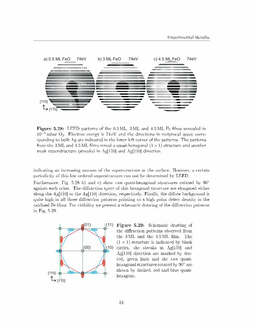
Experimental Results
c) 4.5 ML FeOb) 3 ML FeOa) 0.5 ML FeO 74eV
[1 0]1
[110]
74eV 74eV
(00) (10)
(01) (11)
Figure 5.28: LEED patterns of the 0.5 ML, 3 ML and 4.5 ML Fe �lms annealed in10−5 mbar O2. Electron energy is 74 eV and the directions in reciprocal space corre-sponding to bulk Ag are indicated in the lower left corner of the patterns. The patternsfrom the 3 ML and 4.5 ML �lms reveal a quasi-hexagonal (1× 1) structure and anotherweak superstructure (streaks) in Ag[110] and Ag[110] direction.
indicating an increasing amount of the superstructure at the surface. However, a certainperiodicity of this low ordered superstructure can not be determined by LEED.
Furthermore, Fig. 5.28 b) and c) show two quasi-hexagonal structures rotated by 90◦
against each other. The di�raction spots of this hexagonal structure are elongated eitheralong the Ag[110] or the Ag[110] direction, respectively. Finally, the di�use background isquite high in all three di�raction patterns pointing to a high point defect density in theoxidized Fe �lms. For visibility we present a schematic drawing of the di�raction patternsin Fig. 5.29.
(00) (10)
(01) (11)
[1 0]1
[110]
Figure 5.29: Schematic drawing ofthe di�raction patterns observed fromthe 3 ML and the 4.5 ML �lm. The(1 × 1) structure is indicated by blackcircles, the streaks in Ag[110] andAg[110] direction are marked by dot-ted, green lines and the two quasi-hexagonal structures rotated by 90◦ areshown by dashed, red and blue quasi-hexagons.
81
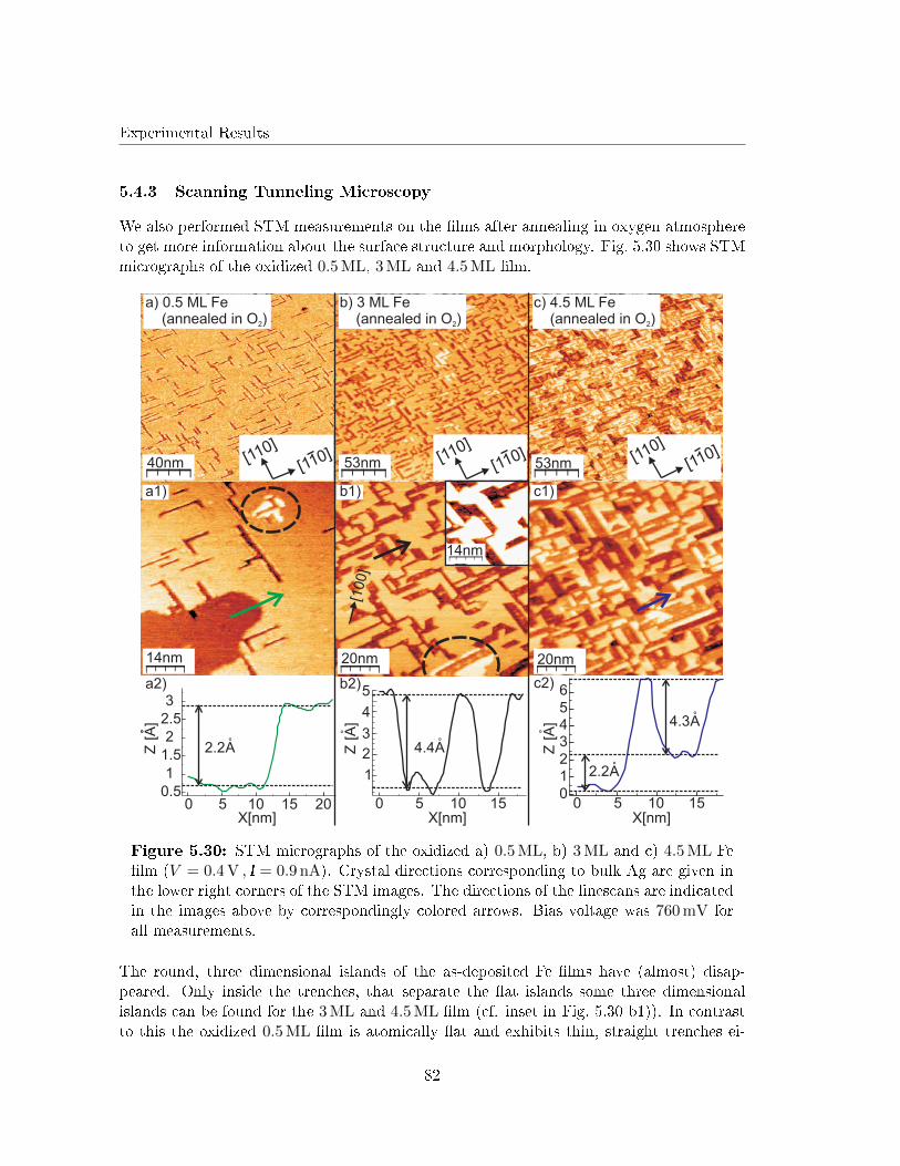
Experimental Results
5.4.3 Scanning Tunneling Microscopy
We also performed STM measurements on the �lms after annealing in oxygen atmosphereto get more information about the surface structure and morphology. Fig. 5.30 shows STMmicrographs of the oxidized 0.5 ML, 3 ML and 4.5 ML �lm.
20151050
3
2.5
2
1.5
1
0.5
X[nm]
Z[A
]
a2)
151050
5
4
3
2
1
X[nm]
Z[A
]
151050
6543210
Z[A
]
X[nm]
b2) c2)
2.2
˚
A 4.4A
2.2A
4.3A
[100]
a) 0.5 ML Fe(annealed in O )2
40nm [110][110]
[110][110]
[110][110]
b) 3 ML Fe(annealed in O )2
c) 4.5 ML Fe(annealed in O )2
53nm 53nm
14nm
14nm 20nm 20nm
a1) b1) c1)
Figure 5.30: STM micrographs of the oxidized a) 0.5 ML, b) 3 ML and c) 4.5 ML Fe�lm (V = 0.4 V , I = 0.9 nA). Crystal directions corresponding to bulk Ag are given inthe lower right corners of the STM images. The directions of the linescans are indicatedin the images above by correspondingly colored arrows. Bias voltage was 760 mV forall measurements.
The round, three dimensional islands of the as-deposited Fe �lms have (almost) disap-peared. Only inside the trenches, that separate the �at islands some three dimensionalislands can be found for the 3 ML and 4.5 ML �lm (cf. inset in Fig. 5.30 b1)). In contrastto this the oxidized 0.5 ML �lm is atomically �at and exhibits thin, straight trenches ei-
82
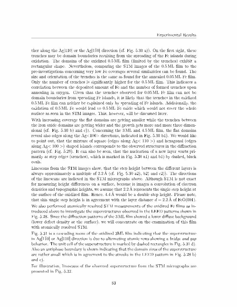
Experimental Results
ther along the Ag[110] or the Ag[110] direction (cf. Fig. 5.30 a)). On the �rst sight, thesetrenches may be domain boundaries resulting from the spreading of the Fe islands duringoxidation. The domains of the oxidized 0.5 ML �lm (limited by the trenches) exhibit arectangular shape. Nevertheless, comparing the STM images of the 0.5 ML �lm to thepre-investigations concerning very low Fe coverages several similarities can be found. Thesize and orientation of the trenches is the same as found for the annealed 0.05 ML Fe �lm.Only the number of trenches is signi�cantly higher for the 0.5 ML �lm. This indicates acorrelation between the deposited amount of Fe and the number of formed trenches uponannealing in oxygen. Given that the trenches observed for 0.05 ML Fe �lm can not bedomain boundaries from spreading Fe islands, it is likely that the trenches in the oxidized0.5 ML Fe �lm can neither be explained only by spreading of Fe islands. Additionally, theoxidation of 0.5 ML Fe would lead to 0.5 ML Fe oxide which would not cover the wholesurface as seen in the STM images. This, however, will be discussed later.
With increasing coverage the �at domains are getting smaller while the trenches betweenthe iron oxide domains are getting wider and the growth gets more and more three dimen-sional (cf. Fig. 5.30 b) and c)). Concerning the 3 ML and 4.5 ML �lm, the �at domainsreveal also edges along the Ag<100> directions, indicated in Fig. 5.30 b1). We would liketo point out, that the mixture of square (edges along Ag< 110 >) and hexagonal (edgesalong Ag< 100 >) shaped islands corresponds to the observed structures in the di�ractionpattern (cf. Fig. 5.28). It can also be seen, that the nucleation of a new layer starts pri-marily at step edges (trenches), which is marked in Fig. 5.30 a1) and b1) by dashed, blackovals.
Linescans from the STM images show, that the step height between the di�erent layers isalways approximately a multiple of 2.2 A (cf. Fig. 5.30 a2), b2) and c2)). The directionsof the linescans are indicted in the STM micrographs above. Although STM is not exactfor measuring height di�erences on a surface, because it images a convolution of electrondensities and topographic heights, we assume that 2.2 A represents the single step height atthe surface of the oxidized �lm. Hence, 4.4 A would be a double step height. Please note,that this single step height is in agreement with the layer distance d = 2.2 A of FeO(001).
We also performed atomically resolved STM measurements of the oxidized Fe �lms as in-troduced above to investigate the superstructures observed in the LEED patterns shown inFig. 5.28. Since the di�raction patterns of the 3 ML �lm showed a lower di�use background(lower defect density at the surface), we will concentrate on the examination of this �lmwith atomically resolved STM.
Fig. 5.31 is a cascading zoom of the oxidized 3ML �lm indicating that the superstructurein Ag[110] or Ag[110] direction is due to alternating atomic rows showing a bridge and gapbehavior. The unit cell of the superstructure is marked by dashed rectangles in Fig. 5.31 d).Also an antiphase boundary is shown indicating that the domain sizes of the superstructureare rather small which is in agreement to the streaks in the LEED pattern in Fig. 5.28 b)and c).
For illustration, linescans of the observed superstructure from the STM micrographs arepresented in Fig. 5.32.
83
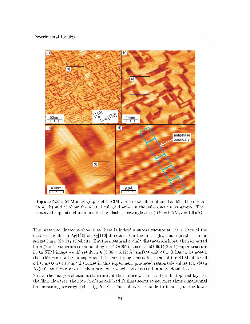
Experimental Results
53nm 14nm
4.0nm 9.8Å
a) b)
c) d)
b)
c)
d)
antiphaseboundary
[110][110]
Figure 5.31: STM micrographs of the 3ML iron oxide �lm obtained at RT. The insetsin a), b) and c) show the related enlarged areas in the subsequent micrograph. Theobserved superstructure is marked by dashed rectangles in d) (V = 0.5 V , I = 1.6 nA).
The presented linescans show that there is indeed a superstructure at the surface of theoxidized Fe �lm in Ag[110] or Ag[110] direction. On the �rst sight, this superstructure issuggesting a (2×1) periodicity. But the measured atomic distances are larger than expectedfor a (2× 1) structure corresponding to FeO(001), since a FeO(001)(2× 1) superstructurein an STM image would result in a (3.06 × 6.12) A2 surface unit cell. It has to be noted,that this can not be an experimental error through misadjustment of the STM, since allother measured atomic distances in this experiment produced reasonable values (cf. cleanAg(001) surface above). This superstructure will be discussed in more detail later.
So far, the analysis of atomic structures at the surface was focused on the topmost layer ofthe �lm. However, the growth of the oxidized Fe �lms seems to get more three dimensionalfor increasing coverage (cf. Fig. 5.30). Thus, it is reasonable to investigate the lower
84
Experimental Results
21.510.50
1.2
1.0
0.8
0.6
0.4
0.2
X[nm]
Z[ Å
]
1.510.50
1.0
0.8
0.6
0.4
2.5
0.9 nm
0.5 nm
a)
9.8Å [110][110]
antiphase boundary
b)
Figure 5.32: a) Linescans taken from the STM image of the 3 ML iron oxide �lmshown in b). The average atomic distance in a row (red linescan) results in aatm =0.5 nm and the average row distance (green linescan) gives arow = 0.9 nm. An antiphaseboundary can be identi�ed by the bigger row distance (black arrow) (V = 0.3 V , I =1.5 nA).
lying visible layers of the �lm. Fig. 5.33 presents a cascading zoom into the second layer(trenches) of the �lm, which is still visible between the topmost islands.
For better visibility we optimized the contrast of the STM image in Fig. 5.33 b) for thesecond layer of the �lm. Hence, the topmost layer looks overexposed. Clearly a hexagonalstructure can be seen in Fig. 5.33 b1). This is in agreement with the di�raction experiments,mentioned above. These hexagonal structured areas seem to be undulated (cf. Fig. 5.33b2)) but their visible size is to small to get quantitative information about a possibleundulation length or height.
Again, we present linescans of the atomically resolved hexagonal structures in Fig. 5.34.Obviously, the observed structure is not hexagonal, but quasi-hexagonal as indicated by theinclined angle between the atomic rows, which is 6= 60◦ as shown in Fig. 5.34. Hence, theatomic distances in the directions of the atomic rows must di�er. Indeed this is the case,since the atomic distance in the direction of the vectors ~a and ~b is aN.N. = bN.N. = 3.45 A.
On the other hand, the next neighbor distance in direction of ~c is only cN.N. = 2.6 A(cf. Fig. 5.34). Although, these values have to be taken with caution because of the lowresolution of the atomically STM images (cf. linescans in Fig. 5.34) it can be concludedthat the second layer of the �lm exhibits an undulated quasi-hexagonal structure.
85
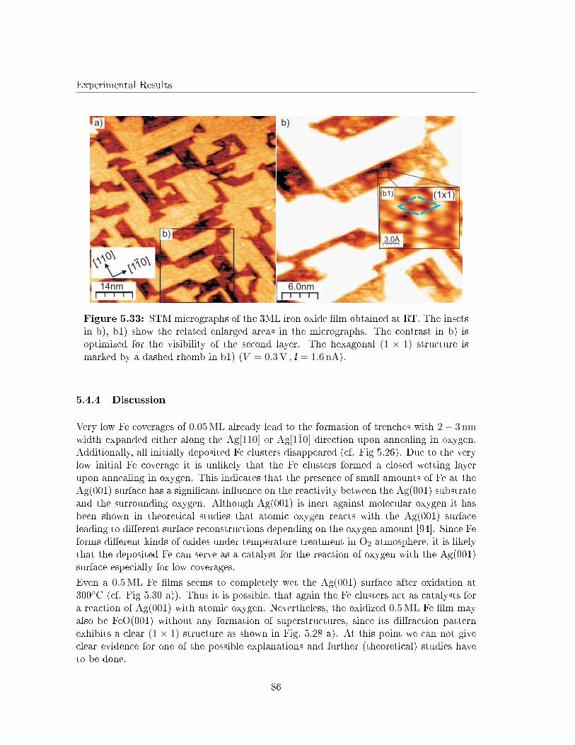
Experimental Results
[110][110]
14nm 6.0nm
3.0Å
(1x1)
a) b)
b1)
b)
Figure 5.33: STM micrographs of the 3ML iron oxide �lm obtained at RT. The insetsin b), b1) show the related enlarged areas in the micrographs. The contrast in b) isoptimized for the visibility of the second layer. The hexagonal (1 × 1) structure ismarked by a dashed rhomb in b1) (V = 0.3 V , I = 1.6 nA).
5.4.4 Discussion
Very low Fe coverages of 0.05 ML already lead to the formation of trenches with 2− 3 nmwidth expanded either along the Ag[110] or Ag[110] direction upon annealing in oxygen.Additionally, all initially deposited Fe clusters disappeared (cf. Fig 5.26). Due to the verylow initial Fe coverage it is unlikely that the Fe clusters formed a closed wetting layerupon annealing in oxygen. This indicates that the presence of small amounts of Fe at theAg(001) surface has a signi�cant in�uence on the reactivity between the Ag(001) substrateand the surrounding oxygen. Although Ag(001) is inert against molecular oxygen it hasbeen shown in theoretical studies that atomic oxygen reacts with the Ag(001) surfaceleading to di�erent surface reconstructions depending on the oxygen amount [94]. Since Feforms di�erent kinds of oxides under temperature treatment in O2 atmosphere, it is likelythat the deposited Fe can serve as a catalyst for the reaction of oxygen with the Ag(001)surface especially for low coverages.
Even a 0.5 ML Fe �lms seems to completely wet the Ag(001) surface after oxidation at300◦C (cf. Fig 5.30 a)). Thus it is possible, that again the Fe clusters act as catalysts fora reaction of Ag(001) with atomic oxygen. Nevertheless, the oxidized 0.5 ML Fe �lm mayalso be FeO(001) without any formation of superstructures, since its di�raction patternexhibits a clear (1 × 1) structure as shown in Fig. 5.28 a). At this point we can not giveclear evidence for one of the possible explanations and further (theoretical) studies haveto be done.
86
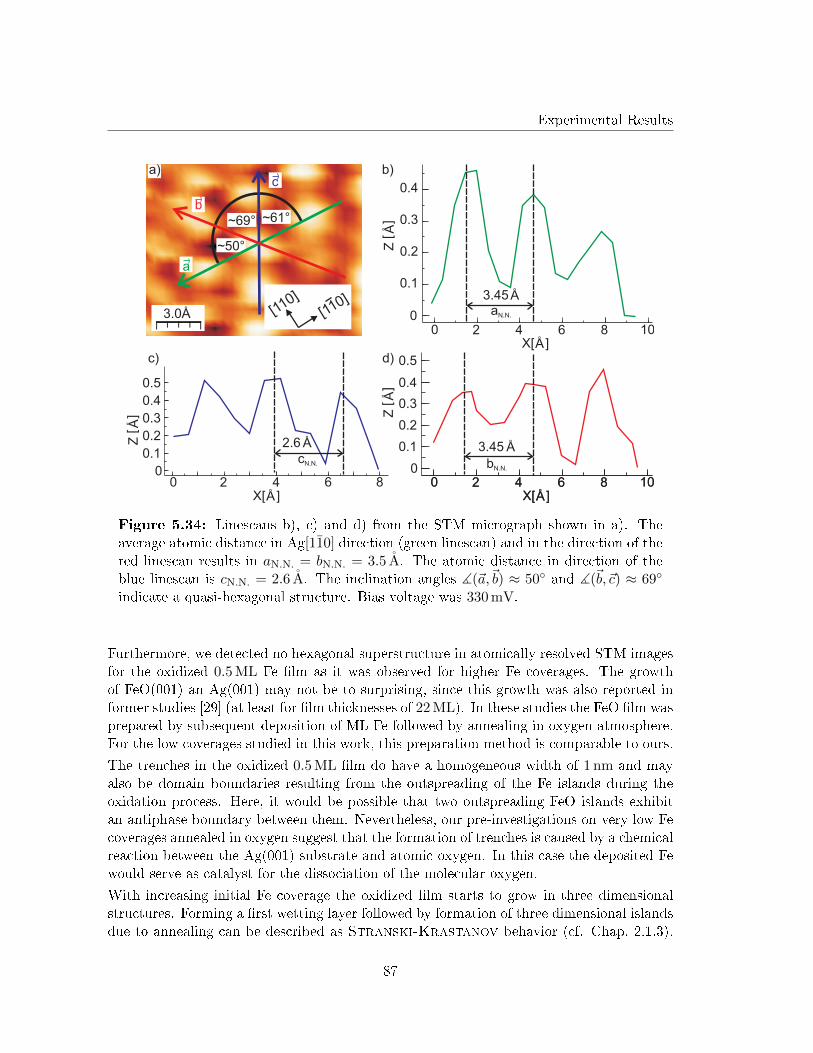
Experimental Results
0.4
0.3
0.2
0.1
0
Z[ Å
]
3.45Å
0.4
0.3
0.2
0
0.5
0.1
1086420X[ ]
3.45 Å
Å
X[ ]Å
Z[ Å
]
1086420X[ ]Å
1086420
0.40.30.2
0
0.5
0.1
Z[ Å
]
86420X[ ]Å
2.6 Å
aN.N.
bN.N.cN.N.
3.0Å [110]
[110]
~50°
a
b
ca) b)
c) d)
~69° ~61°
Figure 5.34: Linescans b), c) and d) from the STM micrograph shown in a). Theaverage atomic distance in Ag[110] direction (green linescan) and in the direction of thered linescan results in aN.N. = bN.N. = 3.5 A. The atomic distance in direction of theblue linescan is cN.N. = 2.6 A. The inclination angles ](~a,~b) ≈ 50◦ and ](~b,~c) ≈ 69◦
indicate a quasi-hexagonal structure. Bias voltage was 330 mV.
Furthermore, we detected no hexagonal superstructure in atomically resolved STM imagesfor the oxidized 0.5 ML Fe �lm as it was observed for higher Fe coverages. The growthof FeO(001) an Ag(001) may not be to surprising, since this growth was also reported informer studies [29] (at least for �lm thicknesses of 22 ML). In these studies the FeO �lm wasprepared by subsequent deposition of ML Fe followed by annealing in oxygen atmosphere.For the low coverages studied in this work, this preparation method is comparable to ours.
The trenches in the oxidized 0.5 ML �lm do have a homogeneous width of 1 nm and mayalso be domain boundaries resulting from the outspreading of the Fe islands during theoxidation process. Here, it would be possible that two outspreading FeO islands exhibitan antiphase boundary between them. Nevertheless, our pre-investigations on very low Fecoverages annealed in oxygen suggest that the formation of trenches is caused by a chemicalreaction between the Ag(001) substrate and atomic oxygen. In this case the deposited Fewould serve as catalyst for the dissociation of the molecular oxygen.
With increasing initial Fe coverage the oxidized �lm starts to grow in three dimensionalstructures. Forming a �rst wetting layer followed by formation of three dimensional islandsdue to annealing can be described as Stranski-Krastanov behavior (cf. Chap. 2.1.3).
87
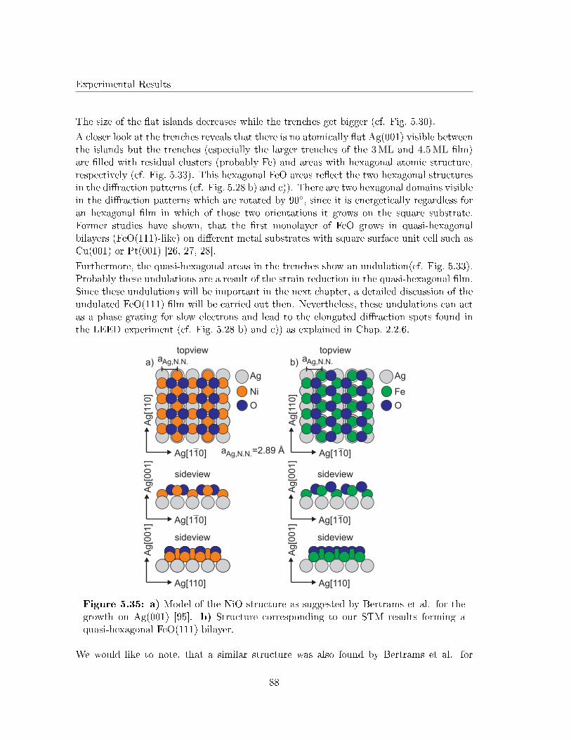
Experimental Results
The size of the �at islands decreases while the trenches get bigger (cf. Fig. 5.30).
A closer look at the trenches reveals that there is no atomically �at Ag(001) visible betweenthe islands but the trenches (especially the larger trenches of the 3 ML and 4.5 ML �lm)are �lled with residual clusters (probably Fe) and areas with hexagonal atomic structure,respectively (cf. Fig. 5.33). This hexagonal FeO areas re�ect the two hexagonal structuresin the di�raction patterns (cf. Fig. 5.28 b) and c)). There are two hexagonal domains visiblein the di�raction patterns which are rotated by 90◦, since it is energetically regardless foran hexagonal �lm in which of those two orientations it grows on the square substrate.Former studies have shown, that the �rst monolayer of FeO grows in quasi-hexagonalbilayers (FeO(111)-like) on di�erent metal substrates with square surface unit cell such asCu(001) or Pt(001) [26, 27, 28].
Furthermore, the quasi-hexagonal areas in the trenches show an undulation(cf. Fig. 5.33).Probably these undulations are a result of the strain reduction in the quasi-hexagonal �lm.Since these undulations will be important in the next chapter, a detailed discussion of theundulated FeO(111) �lm will be carried out then. Nevertheless, these undulations can actas a phase grating for slow electrons and lead to the elongated di�raction spots found inthe LEED experiment (cf. Fig. 5.28 b) and c)) as explained in Chap. 2.2.6.
aAg,N.N.
Ag
Ni
Ag[1 0]1
Ag
[11
0]
O
a =2.89 ÅAg,N.N.
a) aAg,N.N.
Ag
Fe
Ag[1 0]1
Ag
[11
0]
O
b)
Ag[1 0]1
Ag
[00
1]
topview
sideview
Ag[1 0]1
Ag
[00
1]
topview
sideview
Ag[110]
Ag
[00
1]
sideview sideview
Ag[110]
Ag
[00
1]
Figure 5.35: a) Model of the NiO structure as suggested by Bertrams et al. for thegrowth on Ag(001) [95]. b) Structure corresponding to our STM results forming aquasi-hexagonal FeO(111) bilayer.
We would like to note, that a similar structure was also found by Bertrams et al. for
88
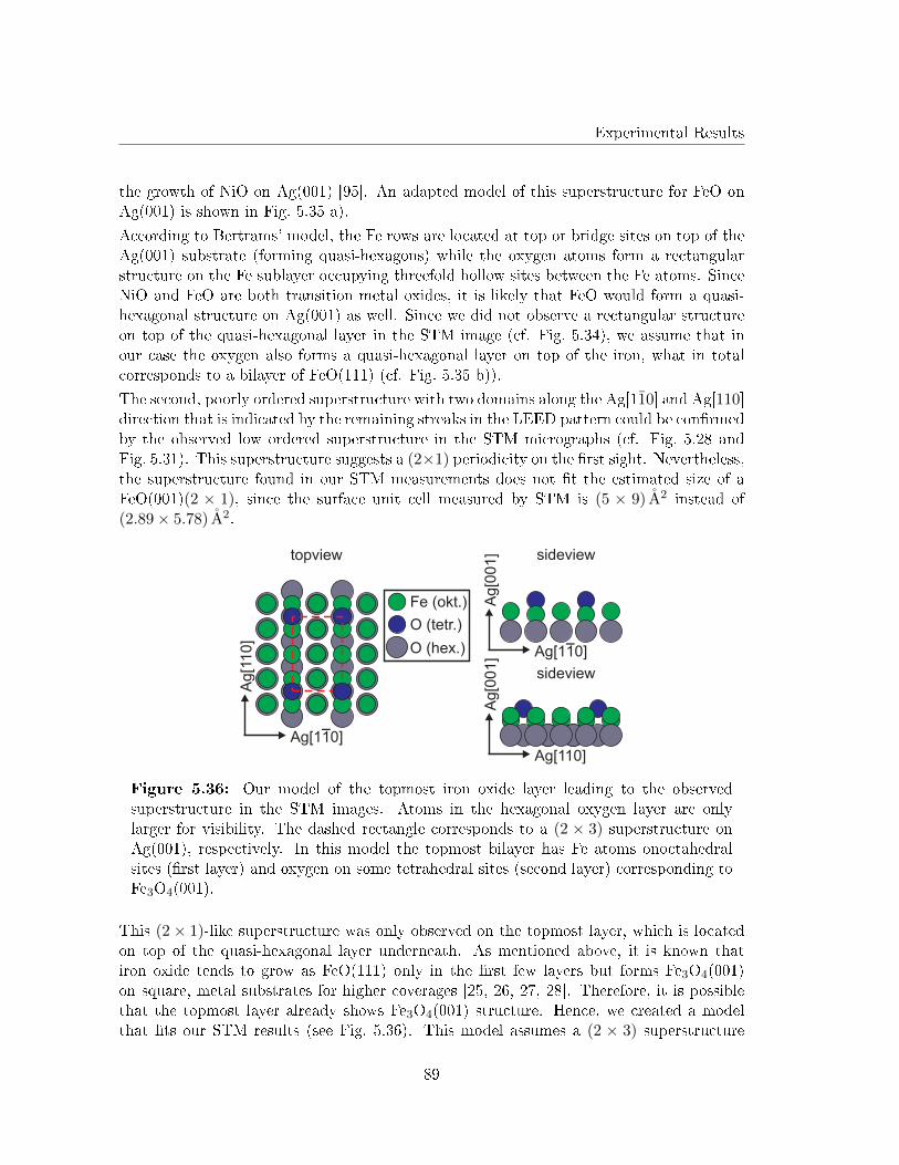
Experimental Results
the growth of NiO on Ag(001) [95]. An adapted model of this superstructure for FeO onAg(001) is shown in Fig. 5.35 a).
According to Bertrams' model, the Fe rows are located at top or bridge sites on top of theAg(001) substrate (forming quasi-hexagons) while the oxygen atoms form a rectangularstructure on the Fe sublayer occupying threefold hollow sites between the Fe atoms. SinceNiO and FeO are both transition metal oxides, it is likely that FeO would form a quasi-hexagonal structure on Ag(001) as well. Since we did not observe a rectangular structureon top of the quasi-hexagonal layer in the STM image (cf. Fig. 5.34), we assume that inour case the oxygen also forms a quasi-hexagonal layer on top of the iron, what in totalcorresponds to a bilayer of FeO(111) (cf. Fig. 5.35 b)).
The second, poorly ordered superstructure with two domains along the Ag[110] and Ag[110]direction that is indicated by the remaining streaks in the LEED pattern could be con�rmedby the observed low ordered superstructure in the STM micrographs (cf. Fig. 5.28 andFig. 5.31). This superstructure suggests a (2×1) periodicity on the �rst sight. Nevertheless,the superstructure found in our STM measurements does not �t the estimated size of aFeO(001)(2 × 1), since the surface unit cell measured by STM is (5 × 9) A2 instead of(2.89× 5.78) A2.
Ag[1 0]1
Ag[1
10]
Fe (okt.)
O (tetr.)
Ag[1 0]1
Ag[0
01]topview sideview
O (hex.)
Ag[110]
Ag[0
01]
sideview
Figure 5.36: Our model of the topmost iron oxide layer leading to the observedsuperstructure in the STM images. Atoms in the hexagonal oxygen layer are onlylarger for visibility. The dashed rectangle corresponds to a (2 × 3) superstructure onAg(001), respectively. In this model the topmost bilayer has Fe atoms onoctahedralsites (�rst layer) and oxygen on some tetrahedral sites (second layer) corresponding toFe3O4(001).
This (2× 1)-like superstructure was only observed on the topmost layer, which is locatedon top of the quasi-hexagonal layer underneath. As mentioned above, it is known thatiron oxide tends to grow as FeO(111) only in the �rst few layers but forms Fe3O4(001)on square, metal substrates for higher coverages [25, 26, 27, 28]. Therefore, it is possiblethat the topmost layer already shows Fe3O4(001) structure. Hence, we created a modelthat �ts our STM results (see Fig. 5.36). This model assumes a (2 × 3) superstructure
89
Experimental Results
corresponding to the Ag(001) substrate (red, dashed rectangle).
In our model the atomic Fe rows in Ag[110] direction at the interface towards the quasi-hexagonal FeO layer occupy alternating octahedral top and bridge sites. The oxygen istetrahedrally coordinated on top of the Fe atoms. It has to be noted, that in a Fe3O4(001)bilayer the tetrahedrally coordinated oxygen would form a (2× 2) superstructure. Hence,the observed superstructure in our model would be an oxygen de�cit structure. This maybe an explanation for the small domains of the superstructure. We would like to pointout, that this model gives only one possible explanation for the observed superstructure.Theoretical calculations have to be done in the future to verify this model.
Nevertheless, we suppose that our oxidized Fe �lms formed partly FeO(001) (for the 0.5 MLFe �lm), as well as FeO(111) and a Fe3O4(001) like structure (for higher coverages) on theAg(001) substrate. Our results suggest, that the topmost layer of the iron oxide �lmis mainly Fe3O4(001) with a poorly ordered (2× 3) superstructure on it, while the quasi-hexagonal FeO(111) surface was only observed at the interface (inside the trenches) between�lm and substrate. It has to be mentioned that there is no study at this time that hasreported both kinds of surface orientation (Fe3O4(001) and FeO(111)) as well as the twosuperstructures for the growth of iron oxide on Ag(001) at the same time.
90
Experimental Results
5.5 Reactive deposition of Fe on Ag(001) in O2 atmosphere
In this chapter Fe oxide �lms grown reactively in 10−5 mbar O2 on Ag(001) will be dis-cussed. The surface structure and morphology of these �lms are studied in detail usingLEED, SPA-LEED and STM while the chemical composition of the �lms is analyzed byXPS. Prior to the measurements we deposited �lms of di�erent thickness (substrate tem-perature 300◦C) on the Ag(001) substrate and calibrated the absolute �lm thickness withquantitative AES (similar to Chap. 5.3). Fig. 5.37 a) presents the AE spectra obtained forthree di�erent �lm thicknesses.
Fe( )LMMAg( )MNN O( )KLL
a)
b)Q
Peak-t
o-p
eak r
atio
Df [Hz]
600 1200 1800 2400
Kinetic energy [eV]
Diff. int. [arb
. units]
Df = 600Hz
Df = 1800Hz
Figure 5.37: a) Exemplary AE spectra obtained from Fe oxide �lms of di�erentthickness on Ag(001). The Fe(LMM)(703eV), the Ag(MNN)(351eV) as well as theO(KLL)(503eV)Auger transitions are indicated by dashed lines. There is no contam-ination (e.g. C(KLL)(271eV)) visible. b) peak-to-peak ratio between the sum of theFe(LMM)(703eV) and the O(KLL)(503eV) signal and the Ag(MNN)(351eV) signal(including the sensitivities σi) over coverage. The coverage in ML was calculated fromEq. 2.69.
In each spectrum the Auger transitions Ag(MNN)(351eV), the O(KLL)(503eV) and theFe(LMM)(703eV) can be seen. As expected the signal of the Ag substrate decreases withincreasing �lm thickness, while the oxygen signal as well as the iron signal increase. Nocontamination of the �lms (e.g. carbon (271eV)) can be detected. Here, it is importantto mention that the prior presented quantitative AES analysis is only exact for laminargrowing �lms without the formation of an interface. Nevertheless, this analysis gives a goodidea about the surface coverage and, therefore, an assignment between mass equivalent ∆fand coverage Θ.
91
Experimental Results
5.5.1 X-Ray Photoelectron Spectroscopy
From the position and shape of the Fe 2p peak in the X-ray photoelectron spectrum one canget information about the iron oxidation state and the stoichiometry of the �lms [96, 97].Fig. 5.38 exemplarily shows the measured Fe 2p doublet of a 1 ML iron oxide �lm as wellas the reference spectra: a) metallic iron (Fe0), b) FeO (Fe2+) and c) Fe2O3 (Fe3+).
Fe 2p1/2
Fe 2p3/2
Inte
nsity
[arb
. u
nits]
Binding energy [eV]
Ag
Sat
Ag 3s
Figure 5.38: X-ray photoelectronspectrum of the measured Fe 2p dou-blet obtained from an iron oxide mono-layer. Reference spectra of a pure Fe�lm, an FeO �lm (Fe2+ spectrum) andFe2O3 �lm (Fe3+ spectrum) are addi-tionally shown. The positions of theFe 2p3/2 and Fe 2p1/2 peaks as well asthe position of the Fe 2p3/2 satellite for
Fe2+ from the reference spectrum aremarked by dotted lines. For compar-ison, the photoelectron spectrum of apure Ag(001) substrate is presented atthe bottom. This spectrum is scaled tothe intensity of the Ag 3d peak in thespectrum of the iron oxide �lm. Thus,the substrate does not show any signif-icant contributions.
The reference spectra were obtained from iron oxide �lms grown under oxygen de�ciencyand oxygen excess on MgO(001), respectively [98]. One can see, that for our sample boththe positions at 706.3 eV and 722.5 eV of the Fe 2p3/2 and Fe 2p1/2 peaks, respectively, as
well as their shapes point to the dominant presence of Fe2+ ions in the �lm. In agreementwith experiments performed on iron oxide �lms on Pt(111) [99] we conclude that FeO(wustite) monolayers grow on Ag(001). Another hint for FeO stoichiometry of the ironoxide �lm is the weak Fe 2p3/2 satellite at 715 eV which does not exist for Fe3O4 where thespectrum shows a plateau without satellites [100]. Also a Ag 3s peak at 719 eV obtainedfrom a pure Ag(001) XPS spectrum can be seen in Fig. 5.38. For reasons of comparison,we scaled this spectrum to the iron oxide �lm using the intensity of the Ag 3d peak at372 eV (not shown here). It can be concluded that the substrate Ag 3s signal from the Agsubstrate has no signi�cant in�uence on the measured Fe 2p signal. It has to be noted, thatthe Fe 2p doublet obtained from thicker samples (not shown here) resulted in an increasingamount of Fe3+ ions with increasing �lm thickness. This indicates the at least partialformation of Fe3O4 (magnetite) within iron oxide �lms with thickness beyond monolayers.
92
Experimental Results
5.5.2 Electron di�raction
We deposited 1 ML Fe oxide �lms on Ag(001) at di�erent substrate temperatures (200◦C,300◦C and 400◦C) in order to determine the optimal growth temperature for our investi-gations. At �rst we investigated the surface structure of the �lms by SPA-LEED. Threeexemplary di�raction patterns (electron energy 108 eV) are shown in Fig. 5.39.
a) 108 eV, 200°C b) 108 eV, 300°C c) 108 eV, 400°C
Ag[1 0]1
Ag[110]
Ag[1 0]1
Ag[110]
Ag[1 0]1
Figure 5.39: Di�raction patterns obtained from the 1 ML Fe oxide �lms grown atdi�erent substrate temperatures. Electron energy is 108 eV for all measurements.
Additional di�raction spots can be seen in all the di�raction patterns compared to the cleanAg(001) substrate. For the Fe oxide �lms grown at 200◦C these additional di�raction spotsare quite weak. The additional di�raction spots as well as the Ag(10) and Ag(01) (andequivalent) spots from the 300◦C sample are split into �ve satellites either along Ag[110] orAg[110] direction. Such satellites can also be seen in the di�raction pattern of the 400◦Csample. Nevertheless, the additional spots from the 400◦C sample are only split into threeweak satellites. Therefore, we will concentrate on the examination of the di�raction patternfrom the Fe oxide �lm grown at 300◦C.
The di�raction pattern presented in Fig. 5.40 a) can be decomposed into three components:(S) a square pattern of sharp di�raction peaks due to the Ag(001) substrate, (A) a hexag-onal structure with di�raction spots which are split into �ve satellites along [110]-directionof the substrate due to the oxide �lm and (B) a second hexagonal pattern due to the oxide�lm which is rotated by 90◦ with respect to the �rst one and aligned in [110]-directionof the substrate. Since the di�raction spots corresponding only to the Ag(001) substrateare not split the satellites are due to the Fe oxide �lm. This agrees with former studieson iron oxide �lms which reported that the growth of a few monolayers of FeO on cubicmetal substrates like Cu(001) or Pt(001) shows (111) orientation [26, 27, 28]. Therefore,we conclude that a FeO(111) �lm growing in two domains was formed on the Ag(001)substrate.
Although, Ag as well as FeO have a cubic bulk structure, the corresponding crystallographicdirections of the FeO monolayer and the Ag(001) substrate are obviously not parallel.Instead, the FeO monolayer grows epitaxially on Ag(001) with (111) orientation so thatthe crystallographic alignments are FeO[111] ‖ Ag[001], FeO[110] ‖ Ag[110] and FeO[112] ‖
93
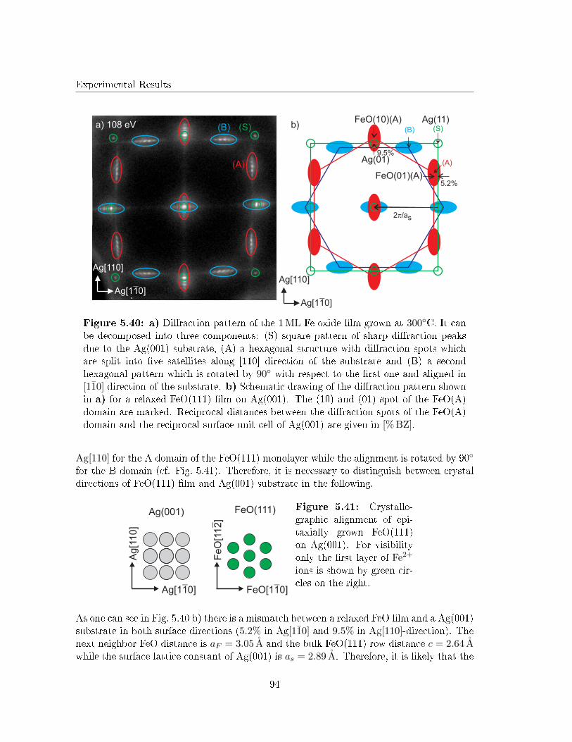
Experimental Results
a) 108 eV (S)
(A)
(B)
9.5%
5.2%
2 /ap
b)FeO(10)(A)
Ag(01)
(S)
(A)
(B)
Ag(11)
s
FeO(01)(A)
Ag[1 0]1
Ag[110]
Ag[1 0]1
Ag[110]
Figure 5.40: a) Di�raction pattern of the 1 ML Fe oxide �lm grown at 300◦C. It canbe decomposed into three components: (S) square pattern of sharp di�raction peaksdue to the Ag(001) substrate, (A) a hexagonal structure with di�raction spots whichare split into �ve satellites along [110] direction of the substrate and (B) a secondhexagonal pattern which is rotated by 90◦ with respect to the �rst one and aligned in[110] direction of the substrate. b) Schematic drawing of the di�raction pattern shownin a) for a relaxed FeO(111) �lm on Ag(001). The (10) and (01) spot of the FeO(A)domain are marked. Reciprocal distances between the di�raction spots of the FeO(A)domain and the reciprocal surface unit cell of Ag(001) are given in [% BZ].
Ag[110] for the A domain of the FeO(111) monolayer while the alignment is rotated by 90◦
for the B domain (cf. Fig. 5.41). Therefore, it is necessary to distinguish between crystaldirections of FeO(111) �lm and Ag(001) substrate in the following.
Ag[1 0]1
Ag
[11
0]
FeO[1 0]1
Fe
O[1
1]
2
Ag(001) FeO(111) Figure 5.41: Crystallo-graphic alignment of epi-taxially grown FeO(111)on Ag(001). For visibilityonly the �rst layer of Fe2+
ions is shown by green cir-cles on the right.
As one can see in Fig. 5.40 b) there is a mismatch between a relaxed FeO �lm and a Ag(001)substrate in both surface directions (5.2% in Ag[110] and 9.5% in Ag[110]-direction). Thenext neighbor FeO distance is aF = 3.05 A and the bulk FeO(111) row distance c = 2.64 Awhile the surface lattice constant of Ag(001) is as = 2.89 A. Therefore, it is likely that the
94
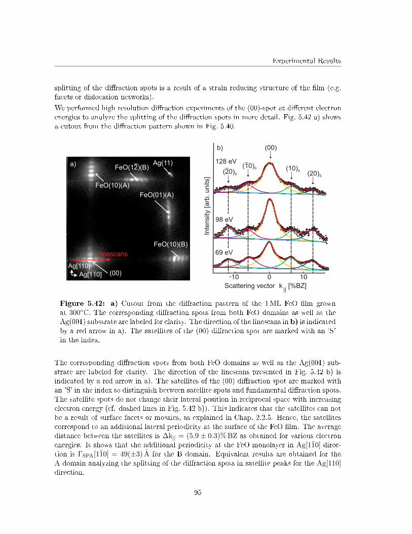
Experimental Results
splitting of the di�raction spots is a result of a strain reducing structure of the �lm (e.g.facets or dislocation networks).
We performed high resolution di�raction experiments of the (00)-spot at di�erent electronenergies to analyze the splitting of the di�raction spots in more detail. Fig. 5.42 a) showsa cutout from the di�raction pattern shown in Fig. 5.40.
(00)
a)
69 eV
( 0)2 S
( 0)1 S
(00)
(20)S
(10)S
Inte
nsity [
arb
. u
nits]
98 eV
128 eV
[%BZ]Scattering vector
b)
linescans
Ag[1 0]1
Ag[110]
Ag(11)
FeO(01)(A)
FeO(1 )(B)2
FeO(10)(B)
FeO(10)(A)
k
Figure 5.42: a) Cutout from the di�raction pattern of the 1 ML FeO �lm grownat 300◦C. The corresponding di�raction spots from both FeO domains as well as theAg(001) substrate are labeled for clarity. The direction of the linescans in b) is indicatedby a red arrow in a). The satellites of the (00) di�raction spot are marked with an 'S'in the index.
The corresponding di�raction spots from both FeO domains as well as the Ag(001) sub-strate are labeled for clarity. The direction of the linescans presented in Fig. 5.42 b) isindicated by a red arrow in a). The satellites of the (00) di�raction spot are marked withan 'S' in the index to distinguish between satellite spots and fundamental di�raction spots.The satellite spots do not change their lateral position in reciprocal space with increasingelectron energy (cf. dashed lines in Fig. 5.42 b)). This indicates that the satellites can notbe a result of surface facets or mosaics, as explained in Chap. 2.2.5. Hence, the satellitescorrespond to an additional lateral periodicity at the surface of the FeO �lm. The averagedistance between the satellites is ∆k|| = (5.9 ± 0.3)% BZ as obtained for various electronenergies. It shows that the additional periodicity at the FeO monolayer in Ag[110] direc-tion is ΓSPA[110] = 49(±3) A for the B domain. Equivalent results are obtained for theA domain analyzing the splitting of the di�raction spots in satellite peaks for the Ag[110]direction.
95
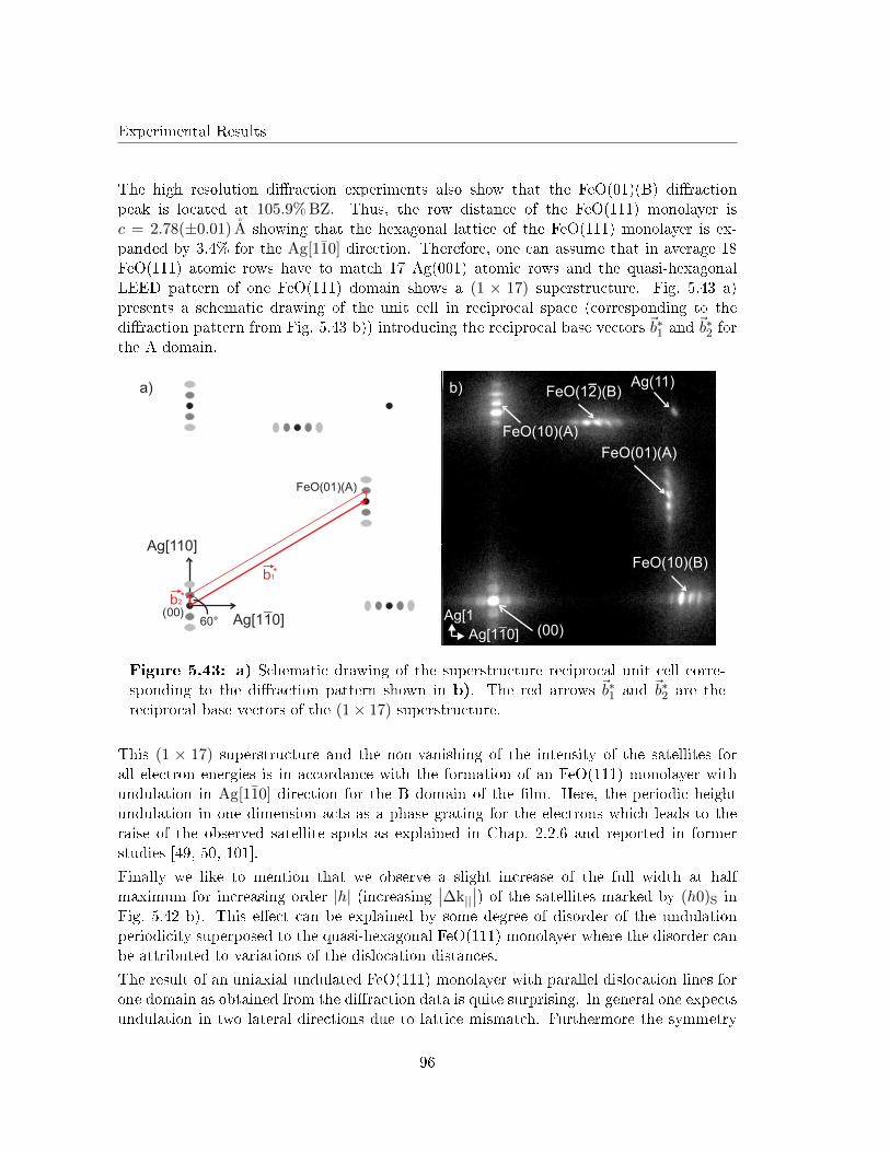
Experimental Results
The high resolution di�raction experiments also show that the FeO(01)(B) di�ractionpeak is located at 105.9% BZ. Thus, the row distance of the FeO(111) monolayer isc = 2.78(±0.01) A showing that the hexagonal lattice of the FeO(111) monolayer is ex-panded by 3.4% for the Ag[110] direction. Therefore, one can assume that in average 18FeO(111) atomic rows have to match 17 Ag(001) atomic rows and the quasi-hexagonalLEED pattern of one FeO(111) domain shows a (1 × 17) superstructure. Fig. 5.43 a)presents a schematic drawing of the unit cell in reciprocal space (corresponding to thedi�raction pattern from Fig. 5.43 b)) introducing the reciprocal base vectors ~b∗1 and
~b∗2 forthe A domain.
(00)
b) Ag(11)
FeO(01)(A)
FeO(1 )(B)2
FeO(10)(B)
FeO(10)(A)
a)
Ag[110]
(00)
b1*
b2*
FeO(01)(A)
60° Ag[1 0]1Ag[1 0]1
Ag[1
Figure 5.43: a) Schematic drawing of the superstructure reciprocal unit cell corre-sponding to the di�raction pattern shown in b). The red arrows ~b∗1 and ~b∗2 are thereciprocal base vectors of the (1× 17) superstructure.
This (1 × 17) superstructure and the non-vanishing of the intensity of the satellites forall electron energies is in accordance with the formation of an FeO(111) monolayer withundulation in Ag[110] direction for the B domain of the �lm. Here, the periodic heightundulation in one dimension acts as a phase grating for the electrons which leads to theraise of the observed satellite spots as explained in Chap. 2.2.6 and reported in formerstudies [49, 50, 101].
Finally we like to mention that we observe a slight increase of the full width at halfmaximum for increasing order |h| (increasing
∣∣∆k||∣∣) of the satellites marked by (h0)S in
Fig. 5.42 b). This e�ect can be explained by some degree of disorder of the undulationperiodicity superposed to the quasi-hexagonal FeO(111) monolayer where the disorder canbe attributed to variations of the dislocation distances.
The result of an uniaxial undulated FeO(111) monolayer with parallel dislocation lines forone domain as obtained from the di�raction data is quite surprising. In general one expectsundulation in two lateral directions due to lattice mismatch. Furthermore the symmetry
96
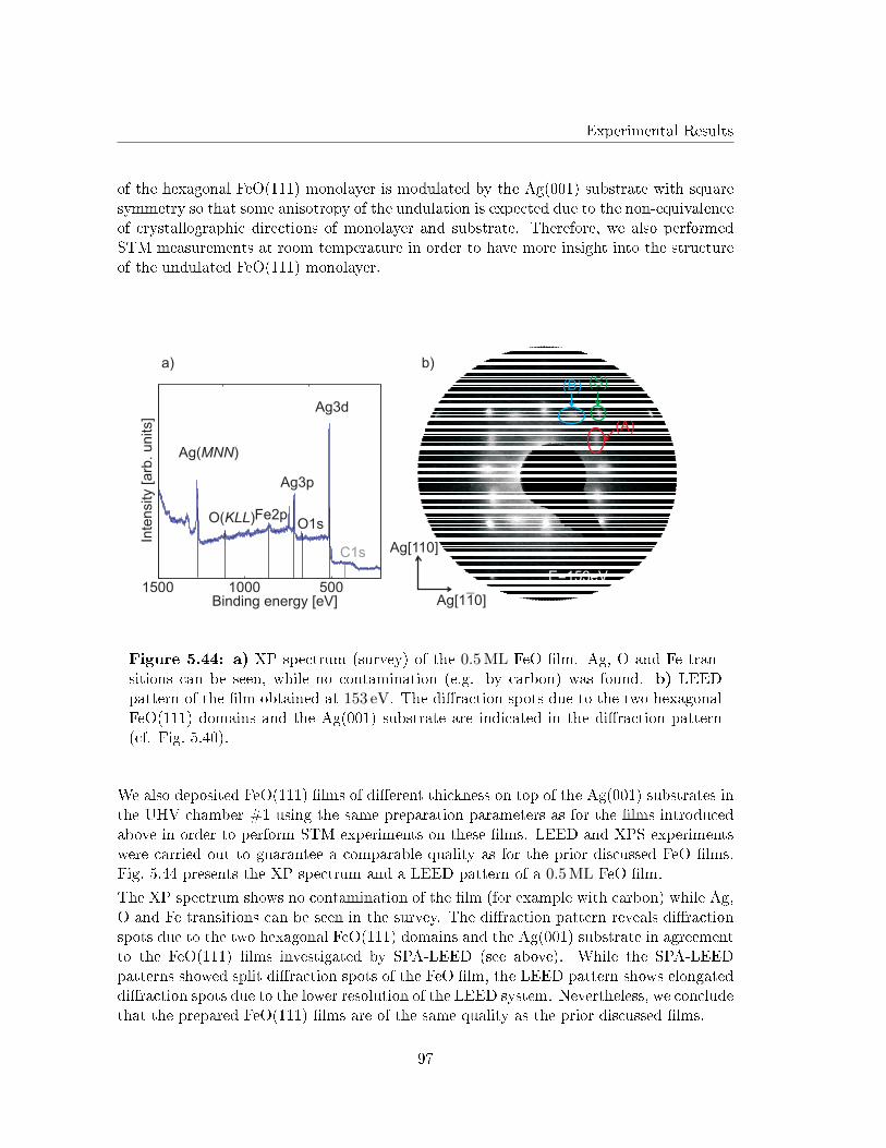
Experimental Results
of the hexagonal FeO(111) monolayer is modulated by the Ag(001) substrate with squaresymmetry so that some anisotropy of the undulation is expected due to the non-equivalenceof crystallographic directions of monolayer and substrate. Therefore, we also performedSTM measurements at room temperature in order to have more insight into the structureof the undulated FeO(111) monolayer.
(S)(B)
(A)
E=153eV
Ag[1 0]1
Ag[110]
Fe2p
Ag3d
O1s
Ag3p
C1s
O( )KLL
Ag( )MNN
a) b)
Binding energy [eV]
Inte
nsity [
arb
. u
nits]
Figure 5.44: a) XP spectrum (survey) of the 0.5 ML FeO �lm. Ag, O and Fe tran-sitions can be seen, while no contamination (e.g. by carbon) was found. b) LEEDpattern of the �lm obtained at 153 eV. The di�raction spots due to the two hexagonalFeO(111) domains and the Ag(001) substrate are indicated in the di�raction pattern(cf. Fig. 5.40).
We also deposited FeO(111) �lms of di�erent thickness on top of the Ag(001) substrates inthe UHV chamber #1 using the same preparation parameters as for the �lms introducedabove in order to perform STM experiments on these �lms. LEED and XPS experimentswere carried out to guarantee a comparable quality as for the prior discussed FeO �lms.Fig. 5.44 presents the XP spectrum and a LEED pattern of a 0.5 ML FeO �lm.
The XP spectrum shows no contamination of the �lm (for example with carbon) while Ag,O and Fe transitions can be seen in the survey. The di�raction pattern reveals di�ractionspots due to the two hexagonal FeO(111) domains and the Ag(001) substrate in agreementto the FeO(111) �lms investigated by SPA-LEED (see above). While the SPA-LEEDpatterns showed split di�raction spots of the FeO �lm, the LEED pattern shows elongateddi�raction spots due to the lower resolution of the LEED system. Nevertheless, we concludethat the prepared FeO(111) �lms are of the same quality as the prior discussed �lms.
97
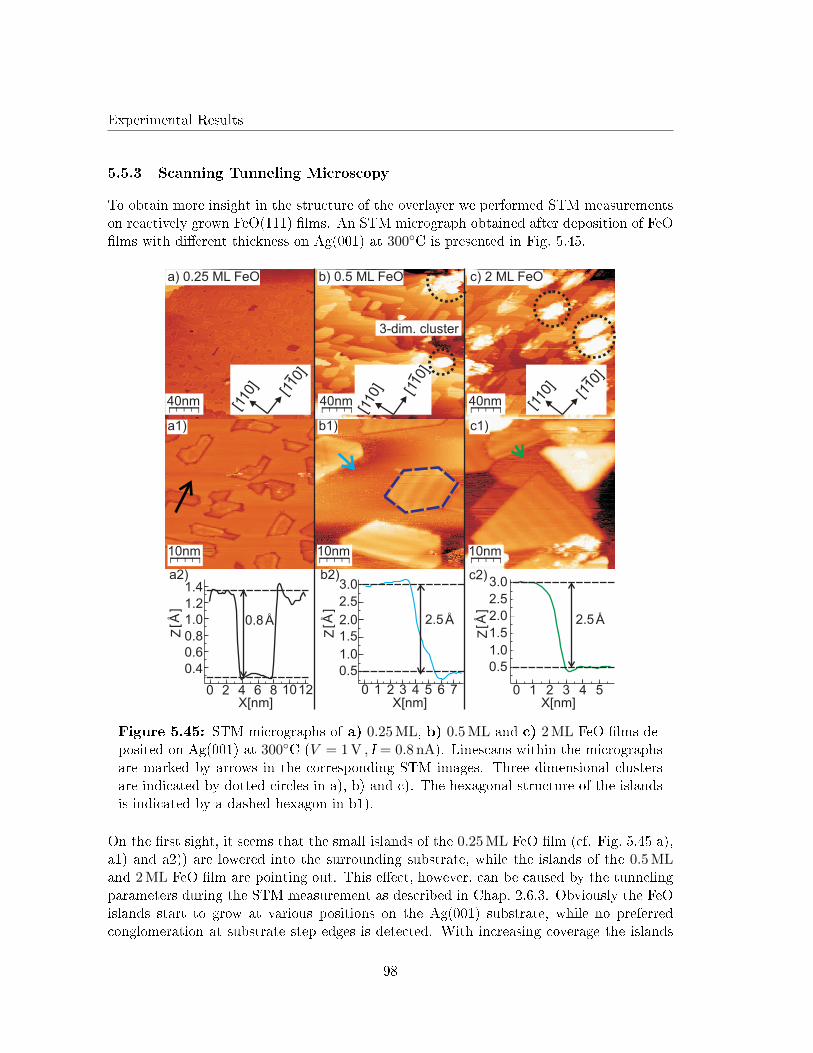
Experimental Results
5.5.3 Scanning Tunneling Microscopy
To obtain more insight in the structure of the overlayer we performed STM measurementson reactively grown FeO(111) �lms. An STM micrograph obtained after deposition of FeO�lms with di�erent thickness on Ag(001) at 300◦C is presented in Fig. 5.45.
10nm10nm
40nm
543210
3.02.52.01.51.00.5
X[nm]
Z[Å
]
2.5Å
76543210
3.02.5
2.01.5
1.00.5
Z[Å
]
X[nm]
2.5Å
121086420
1.41.21.00.80.60.4
X[nm]
Z[Å
]
0.8Å
a2) b2) c2)
a) 0.25 ML FeO b) 0.5 ML FeO c) 2 ML FeO
40nm 40nm 40nm
10nm 10nm 10nm
[110
]
[110
]
3-dim. cluster
[110
]
[110
] [110
]
[110
]
a1) b1) c1)
Figure 5.45: STM micrographs of a) 0.25 ML, b) 0.5 ML and c) 2 ML FeO �lms de-posited on Ag(001) at 300◦C (V = 1 V , I = 0.8 nA). Linescans within the micrographsare marked by arrows in the corresponding STM images. Three dimensional clustersare indicated by dotted circles in a), b) and c). The hexagonal structure of the islandsis indicated by a dashed hexagon in b1).
On the �rst sight, it seems that the small islands of the 0.25 ML FeO �lm (cf. Fig. 5.45 a),a1) and a2)) are lowered into the surrounding substrate, while the islands of the 0.5 MLand 2 ML FeO �lm are pointing out. This e�ect, however, can be caused by the tunnelingparameters during the STM measurement as described in Chap. 2.6.3. Obviously the FeOislands start to grow at various positions on the Ag(001) substrate, while no preferredconglomeration at substrate step edges is detected. With increasing coverage the islands
98
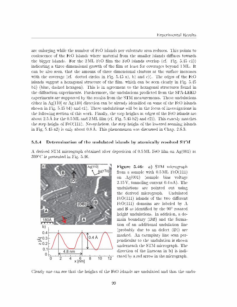
Experimental Results
are enlarging while the number of FeO islands per substrate area reduces. This points tocoalescence of the FeO islands where material from the smaller islands di�uses towardsthe bigger islands. For the 2 ML FeO �lm the FeO islands overlap (cf. Fig. 5.45 c1))indicating a three dimensional growth of the �lm at least for coverages beyond 1 ML. Itcan be also seen, that the amount of three dimensional clusters at the surface increaseswith the coverage (cf. dotted circles in Fig. 5.45 a), b) and c)). The edges of the FeOislands suggest a hexagonal structure of the �lm, which can be seen clearly in Fig. 5.45b1) (blue, dashed hexagon). This is in agreement to the hexagonal structures found inthe di�raction experiments. Furthermore, the undulations predicted from the SPA-LEEDexperiments are supported by the results from the STM measurements. These undulationseither in Ag[110] or Ag[110] direction can be already identi�ed on some of the FeO islandsshown in Fig. 5.45 b1) and c1). These undulations will be in the focus of investigations inthe following section of this work. Finally, the step heights at edges of the FeO islands areabout 2.5 A for the 0.5 ML and 2 ML �lm (cf. Fig. 5.45 b2) and c2)). This exactly matchesthe step height of FeO(111). Nevertheless, the step height of the lowered seeming islandsin Fig. 5.45 a2) is only about 0.8 A. This phenomenon was discussed in Chap. 2.6.3.
5.5.4 Determination of the undulated islands by atomically resolved STM
A derived STM micrograph obtained after deposition of 0.5 ML FeO �lm on Ag(001) at300◦C is presented in Fig. 5.46.
121086420
0.4
0.3
0.2
0.10
x [nm]
z[A
]°
4.8 nm
0.4 Å
b)
180Å
A
A
B
B
(DB)
(D)
a)Ag[1 0]1
Ag[110] Figure 5.46: a) STM micrographfrom a sample with 0.5 ML FeO(111)on Ag(001) (sample bias voltage2.15 V, tunneling current 0.4 nA). Theundulations are pointed out usingthe derived micrograph. UndulatedFeO(111) islands of the two di�erentFeO(111) domains are labeled by Aand B as identi�ed by the 90◦ rotatedheight undulations. In addition, a do-main boundary (DB) and the forma-tion of an additional undulation line(probably due to an defect (D)) aremarked. An exemplary line scan per-pendicular to the undulation is shownunderneath the STM micrograph. Thedirection of the linescan in b) is indi-cated by a red arrow in the micrograph.
Clearly one can see that the heights of the FeO islands are undulated and that the undu-
99
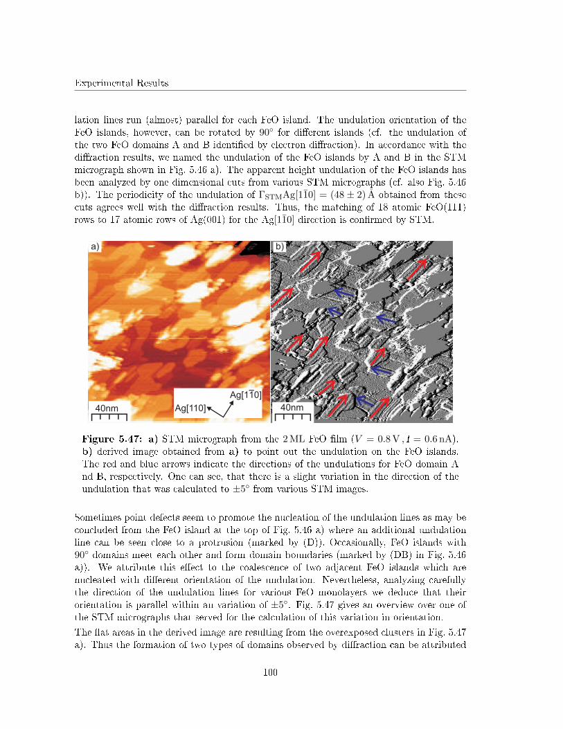
Experimental Results
lation lines run (almost) parallel for each FeO island. The undulation orientation of theFeO islands, however, can be rotated by 90◦ for di�erent islands (cf. the undulation ofthe two FeO domains A and B identi�ed by electron di�raction). In accordance with thedi�raction results, we named the undulation of the FeO islands by A and B in the STMmicrograph shown in Fig. 5.46 a). The apparent height undulation of the FeO islands hasbeen analyzed by one dimensional cuts from various STM micrographs (cf. also Fig. 5.46b)). The periodicity of the undulation of ΓSTMAg[110] = (48 ± 2) A obtained from thesecuts agrees well with the di�raction results. Thus, the matching of 18 atomic FeO(111)rows to 17 atomic rows of Ag(001) for the Ag[110] direction is con�rmed by STM.
40nm40nm Ag[110]
Ag[1 0]1
a) b)
Figure 5.47: a) STM micrograph from the 2 ML FeO �lm (V = 0.8 V , I = 0.6 nA).b) derived image obtained from a) to point out the undulation on the FeO islands.The red and blue arrows indicate the directions of the undulations for FeO domain And B, respectively. One can see, that there is a slight variation in the direction of theundulation that was calculated to ±5◦ from various STM images.
Sometimes point defects seem to promote the nucleation of the undulation lines as may beconcluded from the FeO island at the top of Fig. 5.46 a) where an additional undulationline can be seen close to a protrusion (marked by (D)). Occasionally, FeO islands with90◦ domains meet each other and form domain boundaries (marked by (DB) in Fig. 5.46a)). We attribute this e�ect to the coalescence of two adjacent FeO islands which arenucleated with di�erent orientation of the undulation. Nevertheless, analyzing carefullythe direction of the undulation lines for various FeO monolayers we deduce that theirorientation is parallel within an variation of ±5◦. Fig. 5.47 gives an overview over one ofthe STM micrographs that served for the calculation of this variation in orientation.
The �at areas in the derived image are resulting from the overexposed clusters in Fig. 5.47a). Thus the formation of two types of domains observed by di�raction can be attributed
100
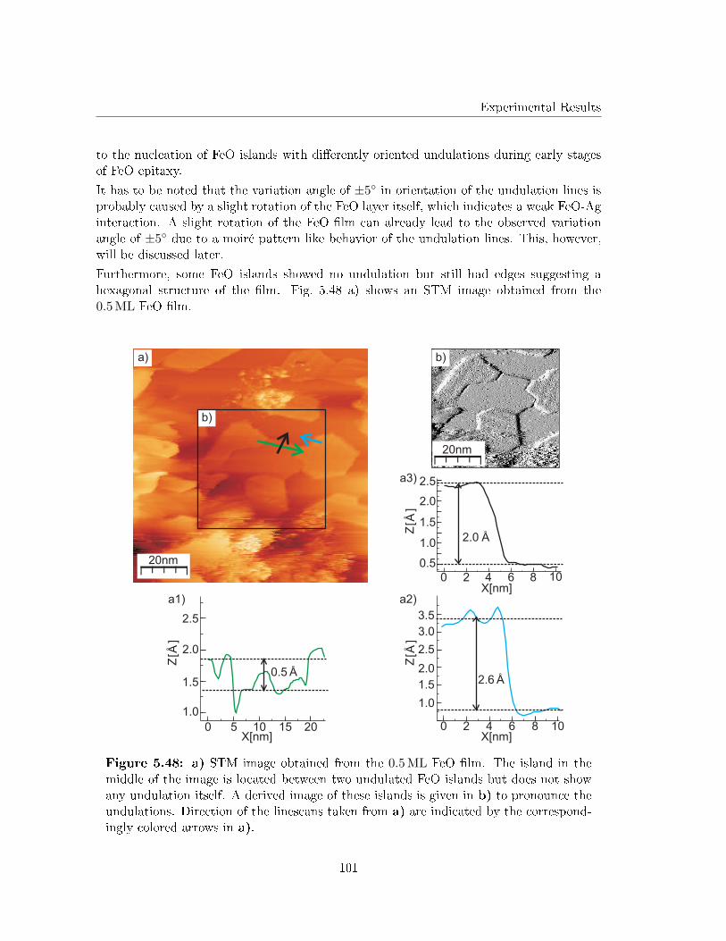
Experimental Results
to the nucleation of FeO islands with di�erently oriented undulations during early stagesof FeO epitaxy.
It has to be noted that the variation angle of ±5◦ in orientation of the undulation lines isprobably caused by a slight rotation of the FeO layer itself, which indicates a weak FeO-Aginteraction. A slight rotation of the FeO �lm can already lead to the observed variationangle of ±5◦ due to a moiré pattern like behavior of the undulation lines. This, however,will be discussed later.
Furthermore, some FeO islands showed no undulation but still had edges suggesting ahexagonal structure of the �lm. Fig. 5.48 a) shows an STM image obtained from the0.5 ML FeO �lm.
20151050
2.5
2.0
1.5
1.0
X[nm]
Z[ Å
]
1086420
3.0
2.0
1.0
X[nm]
1086420
2.5
2.0
1.5
1.0
0.5
X[nm]
Z[ Å
]Z
[ Å]
0.5 Å2.6 Å1.5
2.5
3.5
2.0 Å
a1) a2)
a3)
20nm
20nm
a)
b)
b)
Figure 5.48: a) STM image obtained from the 0.5 ML FeO �lm. The island in themiddle of the image is located between two undulated FeO islands but does not showany undulation itself. A derived image of these islands is given in b) to pronounce theundulations. Direction of the linescans taken from a) are indicated by the correspond-ingly colored arrows in a).
101
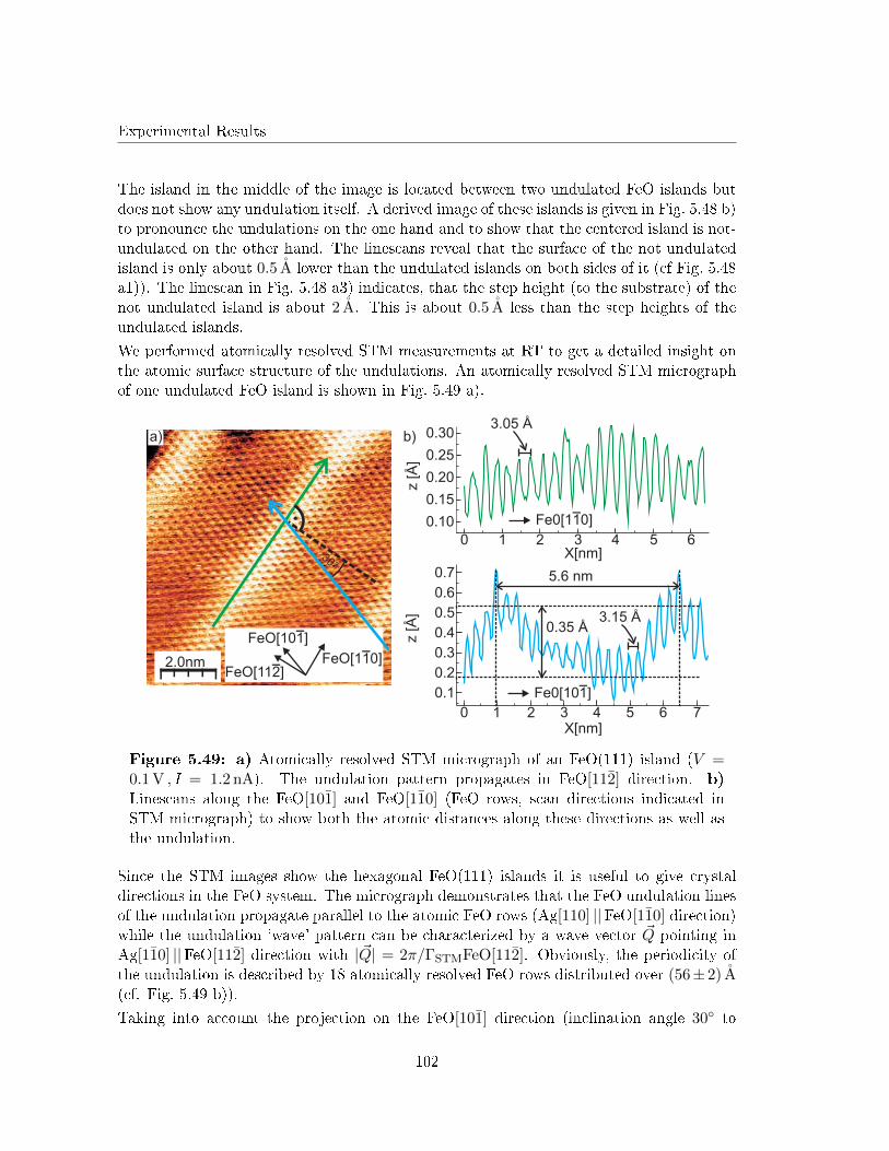
Experimental Results
The island in the middle of the image is located between two undulated FeO islands butdoes not show any undulation itself. A derived image of these islands is given in Fig. 5.48 b)to pronounce the undulations on the one hand and to show that the centered island is not-undulated on the other hand. The linescans reveal that the surface of the not undulatedisland is only about 0.5 A lower than the undulated islands on both sides of it (cf Fig. 5.48a1)). The linescan in Fig. 5.48 a3) indicates, that the step height (to the substrate) of thenot undulated island is about 2 A. This is about 0.5 A less than the step heights of theundulated islands.
We performed atomically resolved STM measurements at RT to get a detailed insight onthe atomic surface structure of the undulations. An atomically resolved STM micrographof one undulated FeO island is shown in Fig. 5.49 a).
6543210
0.30
0.25
0.20
0.15
0.10
X[nm]
z[Å
]3.05 Å
Fe0[1 0]1
76543210
0.7
0.6
0.5
0.4
0.3
0.2
0.1
z[Å
]
X[nm]
Fe0[10 ]1
5.6 nm
30°
0.35 Å
b)
3.15 Å
2.0nmFeO[11 ]2
FeO[1 0]1
FeO[10 ]1
a)
Figure 5.49: a) Atomically resolved STM micrograph of an FeO(111) island (V =0.1 V , I = 1.2 nA). The undulation pattern propagates in FeO[112] direction. b)
Linescans along the FeO[101] and FeO[110] (FeO rows, scan directions indicated inSTM micrograph) to show both the atomic distances along these directions as well asthe undulation.
Since the STM images show the hexagonal FeO(111) islands it is useful to give crystaldirections in the FeO system. The micrograph demonstrates that the FeO undulation linesof the undulation propagate parallel to the atomic FeO rows (Ag[110] ||FeO[110] direction)while the undulation 'wave' pattern can be characterized by a wave vector ~Q pointing inAg[110] ||FeO[112] direction with | ~Q| = 2π/ΓSTMFeO[112]. Obviously, the periodicity ofthe undulation is described by 18 atomically resolved FeO rows distributed over (56± 2) A(cf. Fig. 5.49 b)).
Taking into account the projection on the FeO[101] direction (inclination angle 30◦ to
102
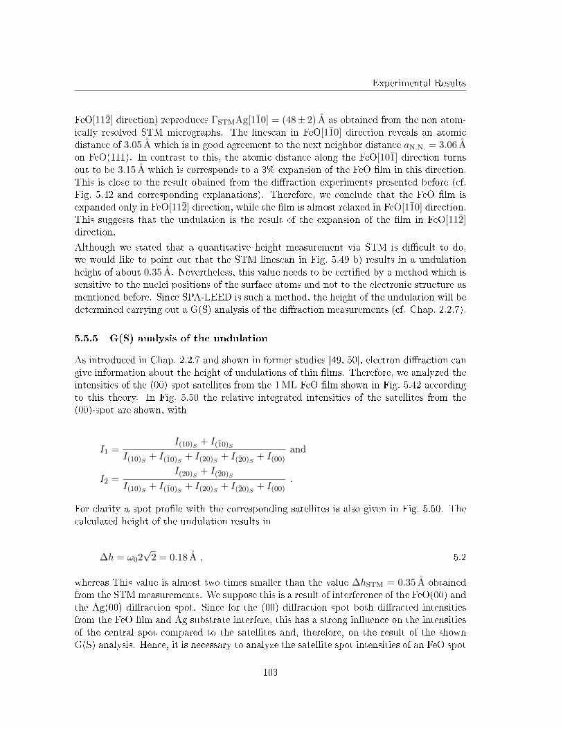
Experimental Results
FeO[112] direction) reproduces ΓSTMAg[110] = (48± 2) A as obtained from the non atom-ically resolved STM micrographs. The linescan in FeO[110] direction reveals an atomicdistance of 3.05 A which is in good agreement to the next neighbor distance aN.N. = 3.06 Aon FeO(111). In contrast to this, the atomic distance along the FeO[101] direction turnsout to be 3.15 A which is corresponds to a 3% expansion of the FeO �lm in this direction.This is close to the result obained from the di�raction experiments presented before (cf.Fig. 5.42 and corresponding explanations). Therefore, we conclude that the FeO �lm isexpanded only in FeO[112] direction, while the �lm is almost relaxed in FeO[110] direction.This suggests that the undulation is the result of the expansion of the �lm in FeO[112]direction.
Although we stated that a quantitative height measurement via STM is di�cult to do,we would like to point out that the STM linescan in Fig. 5.49 b) results in a undulationheight of about 0.35 A. Nevertheless, this value needs to be certi�ed by a method which issensitive to the nuclei positions of the surface atoms and not to the electronic structure asmentioned before. Since SPA-LEED is such a method, the height of the undulation will bedetermined carrying out a G(S) analysis of the di�raction measurements (cf. Chap. 2.2.7).
5.5.5 G(S) analysis of the undulation
As introduced in Chap. 2.2.7 and shown in former studies [49, 50], electron di�raction cangive information about the height of undulations of thin �lms. Therefore, we analyzed theintensities of the (00) spot satellites from the 1 ML FeO �lm shown in Fig. 5.42 accordingto this theory. In Fig. 5.50 the relative integrated intensities of the satellites from the(00)-spot are shown, with
I1 =I(10)S + I(10)S
I(10)S + I(10)S + I(20)S + I(20)S + I(00)and
I2 =I(20)S + I(20)S
I(10)S + I(10)S + I(20)S + I(20)S + I(00).
For clarity a spot pro�le with the corresponding satellites is also given in Fig. 5.50. Thecalculated height of the undulation results in
∆h = ω02√
2 = 0.18 A , 5.2
whereas This value is almost two times smaller than the value ∆hSTM = 0.35 A obtainedfrom the STM measurements. We suppose this is a result of interference of the FeO(00) andthe Ag(00) di�raction spot. Since for the (00) di�raction spot both di�racted intensitiesfrom the FeO �lm and Ag substrate interfere, this has a strong in�uence on the intensitiesof the central spot compared to the satellites and, therefore, on the result of the shownG(S) analysis. Hence, it is necessary to analyze the satellite spot intensities of an FeO spot
103
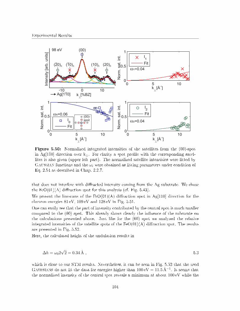
Experimental Results
w1=0.04
w2=0.04
w0=0.06(00)-spot
No
rm.
sat.
int.
( 0)2 S ( 0)1 S
(00)
(20)S(10)S
Inte
nsi
ty [
arb
. u
nits
]98 eV
[%BZ]
No
rm.
sat.
int.
No
rm.
sat.
int.
Ag[1 0]1 k
[Å ]-1k
[Å ]-1k[Å ]-1k
Figure 5.50: Normalized integrated intensities of the satellites from the (00)-spotin Ag[110] direction over k⊥. For clarity a spot pro�le with the corresponding satel-lites is also given (upper left part). The normalized satellite intensities were �tted byGaussian functions and the ωi were obtained as �tting parameters under condition ofEq. 2.54 as described in Chap. 2.2.7.
that does not interfere with di�racted intensity coming from the Ag substrate. We chosethe FeO(01)(A) di�raction spot for this analysis (cf. Fig. 5.43).
We present the linescans of the FeO(01)(A) di�raction spot in Ag[110] direction for theelectron energies 81 eV, 109 eV and 128 eV in Fig. 5.51.
One can easily see that the part of intensity contributed by the central spot is much smallercompared to the (00) spot. This already shows clearly the in�uence of the substrate onthe calculations presented above. Just like for the (00) spot we analyzed the relativeintegrated intensities of the satellite spots of the FeO(01)(A) di�raction spot. The resultsare presented in Fig. 5.52.
Here, the calculated height of the undulation results in
∆h = ω02√
2 = 0.34 A , 5.3
which is close to our STM results. Nevertheless, it can be seen in Fig. 5.52 that the usedGaussians do not �t the data for energies higher than 100 eV = 11.5 A−1. It seems thatthe normalized intensity of the central spot reveals a minimum at about 100 eV while the
104
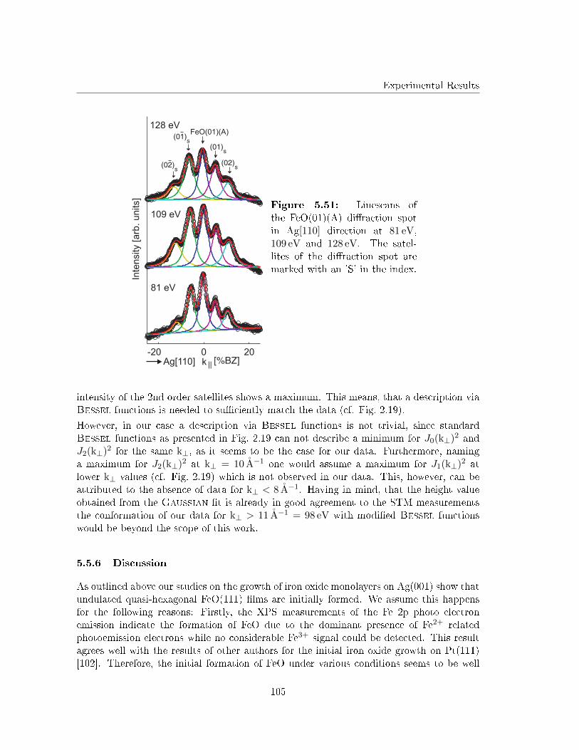
Experimental Results
k ||Ag[110]
Inte
nsity [
arb
. u
nits]
109 eV
128 eV
81 eV
FeO(01)(A)
Figure 5.51: Linescans ofthe FeO(01)(A) di�raction spotin Ag[110] direction at 81 eV,109 eV and 128 eV. The satel-lites of the di�raction spot aremarked with an 'S' in the index.
intensity of the 2nd order satellites shows a maximum. This means, that a description viaBessel functions is needed to su�ciently match the data (cf. Fig. 2.19).
However, in our case a description via Bessel functions is not trivial, since standardBessel functions as presented in Fig. 2.19 can not describe a minimum for J0(k⊥)2 andJ2(k⊥)2 for the same k⊥, as it seems to be the case for our data. Furthermore, naminga maximum for J2(k⊥)2 at k⊥ = 10 A−1 one would assume a maximum for J1(k⊥)2 atlower k⊥ values (cf. Fig. 2.19) which is not observed in our data. This, however, can beattributed to the absence of data for k⊥ < 8 A−1. Having in mind, that the height valueobtained from the Gaussian �t is already in good agreement to the STM measurementsthe conformation of our data for k⊥ > 11 A−1 = 98 eV with modi�ed Bessel functionswould be beyond the scope of this work.
5.5.6 Discussion
As outlined above our studies on the growth of iron oxide monolayers on Ag(001) show thatundulated quasi-hexagonal FeO(111) �lms are initially formed. We assume this happensfor the following reasons: Firstly, the XPS measurements of the Fe 2p photo electronemission indicate the formation of FeO due to the dominant presence of Fe2+ relatedphotoemission electrons while no considerable Fe3+ signal could be detected. This resultagrees well with the results of other authors for the initial iron oxide growth on Pt(111)[102]. Therefore, the initial formation of FeO under various conditions seems to be well
105
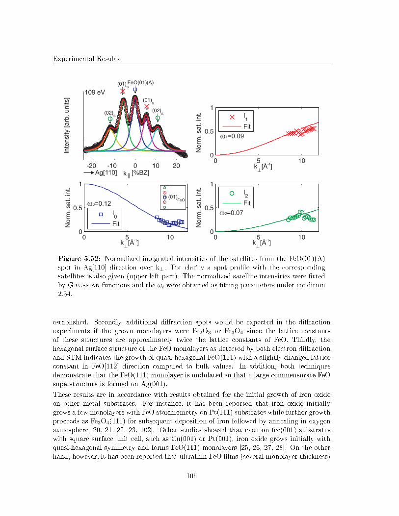
Experimental Results
w0=0.12(01)
FeO
w1=0.09
w2=0.07
No
rm.
sat.
int.
No
rm.
sat.
int.
No
rm.
sat.
int.
[Å ]-1
109 eV
FeO(01)(A)
k ||Ag[110]
Inte
nsi
ty [
arb
. u
nits
]
k
[Å ]-1k[Å ]-1k
Figure 5.52: Normalized integrated intensities of the satellites from the FeO(01)(A)spot in Ag[110] direction over k⊥. For clarity a spot pro�le with the correspondingsatellites is also given (upper left part). The normalized satellite intensities were �ttedby Gaussian functions and the ωi were obtained as �tting parameters under condition2.54.
established. Secondly, additional di�raction spots would be expected in the di�ractionexperiments if the grown monolayers were Fe2O3 or Fe3O4 since the lattice constantsof these structures are approximately twice the lattice constants of FeO. Thirdly, thehexagonal surface structure of the FeO monolayers as detected by both electron di�ractionand STM indicates the growth of quasi-hexagonal FeO(111) with a slightly changed latticeconstant in FeO[112] direction compared to bulk values. In addition, both techniquesdemonstrate that the FeO(111) monolayer is undulated so that a large commensurate FeOsuperstructure is formed on Ag(001).
These results are in accordance with results obtained for the initial growth of iron oxideon other metal substrates. For instance, it has been reported that iron oxide initiallygrows a few monolayers with FeO stoichiometry on Pt(111) substrates while further growthproceeds as Fe3O4(111) for subsequent deposition of iron followed by annealing in oxygenatmosphere [20, 21, 22, 23, 102]. Other studies showed that even on fcc(001) substrateswith square surface unit cell, such as Cu(001) or Pt(001), iron oxide grows initially withquasi-hexagonal symmetry and forms FeO(111) monolayers [25, 26, 27, 28]. On the otherhand, however, it has been reported that ultrathin FeO �lms (several monolayer thickness)
106
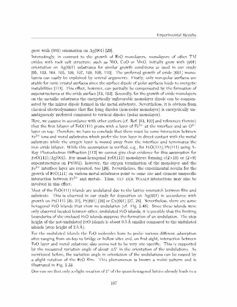
Experimental Results
grow with (001) orientation on Ag(001) [29].
Interestingly, in contrast to the growth of FeO monolayers, monolayers of other TMoxides with rock salt structure, such as NiO, CoO or MnO, initially grow with (001)orientation on Ag(001) substrates for similar growth conditions as used in our study[95, 103, 104, 105, 106, 107, 108, 109, 110]. The preferred growth of oxide (001) mono-layers can easily be explained by several arguments. Firstly, only non-polar surfaces arestable for ionic crystal surfaces since the surface dipole of polar surfaces leads to energeticinstabilities [111]. This e�ect, however, can partially be compensated by the formation ofsuperstructures at the oxide surface [13, 102]. Secondly, for the growth of oxide monolayerson the metallic substrates the energetically unfavorable monolayer dipole can be compen-sated by the mirror dipole formed in the metal substrate. Nevertheless, it is obvious fromclassical electrodynamics that �at lying dipoles (non-polar monolayer) is energetically un-ambiguously preferred compared to vertical dipoles (polar monolayer).
Here, we assume in accordance with other authors (cf. Ref. [13, 102] and references therein)that the �rst bilayer of FeO(111) grows with a layer of Fe2+ at the interface and an O2−
layer on top. Therefore, we have to conclude that there must be some interaction betweenFe2+ ions and metal substrates which prefer the iron layer in direct contact with the metalsubstrate while the oxygen layer is moved away from the interface and terminates theiron oxide bilayer. While this assumption is veri�ed, e.g., for FeO(111)/Pt(111) using X-Ray Photoelectron Di�raction [112] we cannot give clear evidence for this assumption forFeO(111)/Ag(001). For quasi-hexagonal FeO(111) monolayers forming c(2×10) or (2×9)superstructures on Pt(001), however, the oxygen termination of the monolayer and theFe2+ interface layer are reported, too [26]. Nevertheless, the experimental results for thegrowth of FeO(111) on various metal substrates point to some site and element unspeci�cinteraction between Fe2+ and metals. Thus, van der Waals interactions may also beinvolved in this e�ect.
Most of the FeO(111) islands are undulated due to the lattice mismatch between �lm andsubstrate. This is observed in our study for deposition on Ag(001) in accordance withgrowth on Pt(111) [20, 21], Pt(001) [26] or Cu(001) [27, 28]. Nevertheless, there are somehexagonal FeO islands that show no undulation (cf. Fig. 5.48). Since these islands wereonly observed located between other, undulated FeO islands, it is possible that the limitingboundaries of the enclosed FeO islands suppress the formation of an undulation. The stepheight of the not-undulated FeO islands is about 0.5 A smaller compared to the undulatedislands (step height of 2.5 A).
For the undulated islands the FeO molecules have to probe various di�erent adsorptionsites ranging from on-top to bridge or hollow sites and, on �rst sight, interaction betweenFeO layer and metal substrate also seems not to be very site speci�c. This is supportedby the measured variation angle of about ±5◦ in the orientation of the undulations. Asmentioned before, the variation angle in orientation of the undulations can be caused bya slight rotation of the FeO �lm. This phenomenon is known a moiré pattern and isillustrated in Fig. 5.53.
One can see that only a slight rotation of 1◦ of the quasi-hexagonal lattice already leads to a
107
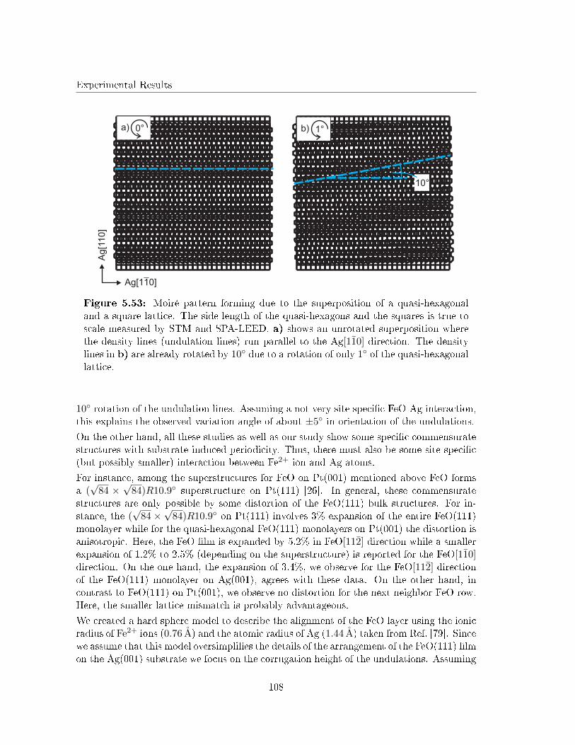
Experimental Results
0°
10°
a) 1°b)
Ag[1 0]1
Figure 5.53: Moiré pattern forming due to the superposition of a quasi-hexagonaland a square lattice. The side length of the quasi-hexagons and the squares is true toscale measured by STM and SPA-LEED. a) shows an unrotated superposition wherethe density lines (undulation lines) run parallel to the Ag[110] direction. The densitylines in b) are already rotated by 10◦ due to a rotation of only 1◦ of the quasi-hexagonallattice.
10◦ rotation of the undulation lines. Assuming a not very site speci�c FeO-Ag interaction,this explains the observed variation angle of about ±5◦ in orientation of the undulations.
On the other hand, all these studies as well as our study show some speci�c commensuratestructures with substrate induced periodicity. Thus, there must also be some site speci�c(but possibly smaller) interaction between Fe2+ ion and Ag atoms.
For instance, among the superstructures for FeO on Pt(001) mentioned above FeO formsa (√
84 ×√
84)R10.9◦ superstructure on Pt(111) [26]. In general, these commensuratestructures are only possible by some distortion of the FeO(111) bulk structures. For in-stance, the (
√84 ×
√84)R10.9◦ on Pt(111) involves 3% expansion of the entire FeO(111)
monolayer while for the quasi-hexagonal FeO(111) monolayers on Pt(001) the distortion isanisotropic. Here, the FeO �lm is expanded by 5.2% in FeO[112] direction while a smallerexpansion of 1.2% to 2.5% (depending on the superstructure) is reported for the FeO[110]direction. On the one hand, the expansion of 3.4%, we observe for the FeO[112] directionof the FeO(111) monolayer on Ag(001), agrees with these data. On the other hand, incontrast to FeO(111) on Pt(001), we observe no distortion for the next neighbor FeO row.Here, the smaller lattice mismatch is probably advantageous.
We created a hard sphere model to describe the alignment of the FeO layer using the ionicradius of Fe2+ ions (0.76 A) and the atomic radius of Ag (1.44 A) taken from Ref. [79]. Sincewe assume that this model oversimpli�es the details of the arrangement of the FeO(111) �lmon the Ag(001) substrate we focus on the corrugation height of the undulations. Assuming
108
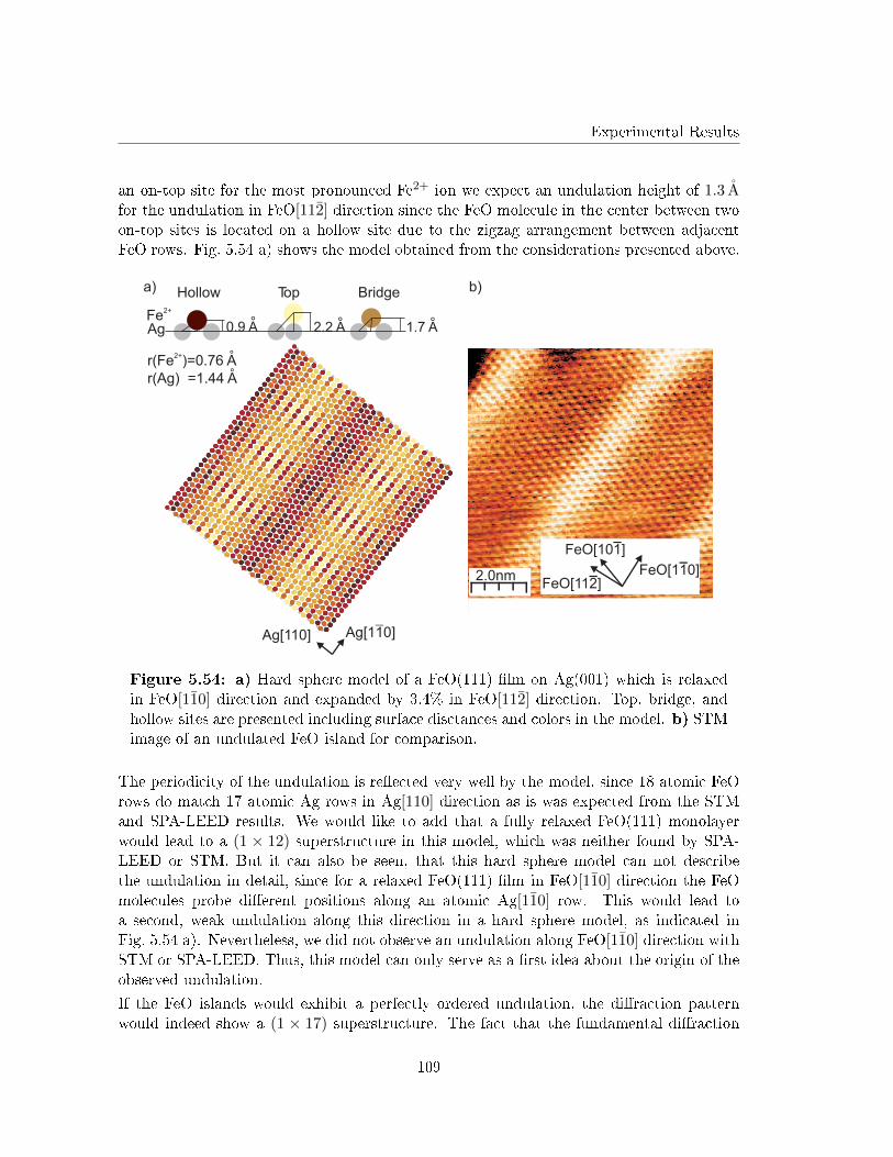
Experimental Results
an on-top site for the most pronounced Fe2+ ion we expect an undulation height of 1.3 Afor the undulation in FeO[112] direction since the FeO molecule in the center between twoon-top sites is located on a hollow site due to the zigzag arrangement between adjacentFeO rows. Fig. 5.54 a) shows the model obtained from the considerations presented above.
1.7 A°0.9 A° 2.2 A°
Hollow Top Bridgea) b)
Ag[1 0]1Ag[110]
r(Fe )=0.76 A2+ °
r(Ag) =1.44 A°
Fe2+
Ag
2.0nmFeO[11 ]2
FeO[1 0]1
FeO[10 ]1
Figure 5.54: a) Hard sphere model of a FeO(111) �lm on Ag(001) which is relaxedin FeO[110] direction and expanded by 3.4% in FeO[112] direction. Top, bridge, andhollow sites are presented including surface disctances and colors in the model. b) STMimage of an undulated FeO island for comparison.
The periodicity of the undulation is re�ected very well by the model, since 18 atomic FeOrows do match 17 atomic Ag rows in Ag[110] direction as is was expected from the STMand SPA-LEED results. We would like to add that a fully relaxed FeO(111) monolayerwould lead to a (1 × 12) superstructure in this model, which was neither found by SPA-LEED or STM. But it can also be seen, that this hard sphere model can not describethe undulation in detail, since for a relaxed FeO(111) �lm in FeO[110] direction the FeOmolecules probe di�erent positions along an atomic Ag[110] row. This would lead toa second, weak undulation along this direction in a hard sphere model, as indicated inFig. 5.54 a). Nevertheless, we did not observe an undulation along FeO[110] direction withSTM or SPA-LEED. Thus, this model can only serve as a �rst idea about the origin of theobserved undulation.
If the FeO islands would exhibit a perfectly ordered undulation, the di�raction patternwould indeed show a (1 × 17) superstructure. The fact that the fundamental di�raction
109
Experimental Results
spots do only exhibit satellites up to second order can be attributed to two things. Firstly,a degree of disorder in the size of the undulation and secondly, the relatively small share ofundulated FeO islands compared to the whole surface. The average value of ΓSTMAg[110] =(48 ± 2) A indicates that the size of an undulations can vary from 17 to 19 FeO atomicrows. This variation bene�ts the vanishing of the satellites spots for higher orders.
The G(S) analysis of the undulation height was problematic for the (00) spot due tointerference of di�racted intensity from FeO �lm and Ag(001) substrate. In contrast tothis, former studies concerning Ge �lms on Si(111) and Ag �lms on Si(001) were able toperform a G(S) analysis at the (00) spot [49, 50]. Here, the observed �lms were muchthicker compared to our FeO �lm (16 nm Ge and 20 nm Ag �lms). Since the mean freepath of slow electrons is much smaller than 16 nm, there is no remaining di�racted intensityfrom the substrates which would lead to a superposition of substrate and �lm signal. Wesolved this problem by analyzing the satellite spot intensities of the FeO(01)(A) spot (cf.Fig. 5.52) where no Ag(001) di�raction spot interferes with the measured intensity.
The obtained corrugation of the FeO �lm of ∆h = ω02√
2 = 0.34 A is in the same magni-tude and, therefore, good agreement to the corrugations quanti�ed in the studies mentionedabove [49, 50]. In addition, the G(S) analysis of the FeO(01)(A) spot re�ects well the re-sults of the STM measurements. As mentioned before, a height measurement with STMis di�cult to handle. We still assume the value of ∆hSTM = 0.35 A to be reliable, since aFeO(111) surface consists only of O2− or Fe2+ ions. Hence, the electronic structure shouldbe similar for every atom at the surface of an FeO(111) island. Of course, the corrugationof the surface, and therefore the position of the surface atoms over the Ag substrate, mayhave an in�uence on the electronic structure at the surface. Nevertheless, we assume thisin�uence to be small for FeO(111) �lms growing in bilayers (Fe2+ layer at the interfaceand O2− layer on top), since the relevant electronic in�uence for the topmost atomic layerwill come from the underlaying and is, therefore, comparable for every surface atom.
In summary, we have demonstrated that reactively deposited iron oxide initially grows asFeO (wustite) layer on Ag(001). Detailed analysis of SPA-LEED and STM experimentsshowed that the FeO(111) structure of the oxide �lm is undulated and forms a commensu-rate superstructure with respect to the Ag(001) substrate. Therefore, the quasi-hexagonalstructure of the FeO(111) layer is distorted with respect to its bulk structure.
110
Conclusion
6 Conclusion
In a �rst step we analyzed the Ag segregation due to UHV annealing of ultrathin Fe �lms onAg(001) at 300◦C as observed in former studies [30, 31]. The Ag segregation was con�rmedby AES and XPS. STM suggests a drastic change in surface structure upon annealing inUHV. The round, column-shaped Fe islands from the as-deposited �lms disappeared andthe surface exhibits large, atomically �at areas with a square (1 × 1) surface unit cellcorresponding to Ag(001). Three dimensional islands of about 5 A height and branchedstructures are likely to be remaining Fe at the surface. Since the Fe in these islands andbranched structures observed by STM is much less than expected from the AES and XPSmeasurements, we assume that Fe is buried underneath the �at Ag(001) areas. This issupported by energetic considerations.
Furthermore, electron di�raction suggests a (√
2×√
2)R45◦ superstructure after annealingof the Fe �lms in UHV. This superstructure, however, could not be resolved via STM. Theatomically �at Ag(001) areas showed no superstructure and the Fe islands and branchedstructures did not allow an atomic resolution with STM due to their strongly three di-mensional structure. Nevertheless, the (
√2 ×√
2)R45◦ superstructure observed in thedi�raction patterns has not been reported in connection to the segregation of Ag on UHVannealed Fe �lms before.
Afterward we analyzed the changes in surface structure due to annealing of Fe �lms onAg(001) in O2 atmosphere. Our pre-investigations concerning very low Fe coverages of0.05 ML suggest a signi�cant in�uence of the Fe on the reactivity of the Ag(001) surface.Here, the surface forms trenches of 2− 3 nm width expanded along Ag[110] or Ag[110] di-rection, respectively. Although it is known that Ag(001) is inert against molecular oxygen,the Ag(001) forms di�erent reconstructions due to exposure to atomic oxygen [94]. It islikely that the atomic oxygen is provided by the Fe oxides formed at the Ag(001) surfaceduring annealing in O2 atmosphere. Hence, Fe acts as a catalyst for the oxidation of theAg(001) surface.
Up to an Fe coverage of 0.5 ML the oxidized �lms wet the substrate. No superstructurescan be seen in atomically resolved STM micrographs and the di�raction patterns showclear (1×1) structures. With increasing initial Fe coverage the oxidized �lms start to formthree dimensional structures (Stranski-Krastanov behavior). The topmost layer of theoxidized �lms (for coverages above 3 ML) is Fe3O4(001)-like with a poorly ordered (3× 2)superstructure on it (cf. Fig. 5.32).
The layers underneath, which are visible due to the Stranski-Krastanov behavior ofthe annealed �lms, exhibit a hexagonal surface structure. An inspection of the atomic nextneighbor distances on this hexagonal structure reveals that it is in fact quasi-hexagonal.This is due an expansion of the hexagonal structure in one direction (cf. Fig. 5.34). Ad-ditionally, these hexagonal layers are undulated either along Ag[110] or Ag[110] direction,but the visible areas are to small to give quantitative information about undulation heightsors lengths (cf. Fig. 5.33). Nevertheless, the corresponding di�raction patterns showed twoquasi-hexagonal structures, which are rotated by 90◦ con�rming the STM results. In ac-
111
Conclusion
cordance with former studies we assume these hexagonal layers to be FeO(111). Thosestudies reported the initial growth of FeO(111)-like iron oxide on Cu(001) or Pt(001),while Fe3O4(001) formation was reported for higher coverages [25, 26, 27, 28]. It has tobe mentioned that there is no study at this time that has reported both kinds of surfaceorientation (Fe3O4(001) and FeO(111)) as well as the two superstructures for the growthof iron oxide on Ag(001) at the same time.
Finally we analyzed the reactive growth of Fe oxide by deposition of Fe in an O2 atmo-sphere. Similar to the post deposition annealed (PDA) Fe oxide �lms, the here obtaineddi�raction patterns show two quasi-hexagonal structures, which are rotated by 90◦ againsteach other. On the other hand, no streaks in Ag[110] or Ag[110] direction are observed inthe di�raction patterns. XPS measurements suggest a dominant presence of Fe2+ relatedphotoemission electrons while no considerable Fe3+ signal could be detected. Therefore,we assume that quasi-hexagonal FeO(111) �lms in two orthogonal domains are initiallyformed by reactive deposition of Fe on Ag(001).
The di�raction spots of the quasi hexagonal FeO(111) �lm are split into several satellitespots either along Ag[110] or Ag[110] direction. For a substrate temperature of 300◦C�ve satellites can be seen, while for higher temperatures the number of satellite spotsdecreases. These satellites do not change their position in reciprocal space with increasingscattering phase pointing to an additional periodicity at the surface of the FeO(111) �lm.This additional periodicity was found to be an undulation as con�rmed by STM. Theundulation lines run parallel to the atomic FeO rows within a variation angle of ±5◦. Ithas to be mentioned that a slight rotation of the FeO(111) �lm can already lead to asigni�cant rotation of the undulation lines due to a moiré pattern behavior. Hence, theinteraction between FeO layer and metal substrate seems not to be very site speci�c.
The average undulation length determined by SPA-LEED and STM is D = (48 ± 2) Acorresponding to a (1×17) superstructure. The height of the undulation was measured viaSTM and calculated by a G(S) analysis of the satellite spot intensities from the di�ractionexperiments. This results in an average undulation height of 0.34 A.
Atomically resolved STM micrographs show an expansion of 3.4% in FeO[112] direction forboth domains of the FeO(111) �lm. This expansion can lead to the observed undulation asshown in the hard shepre model. Nevertheless, this model can not describe the undulationin detail since secondary undulations alon the FeO[110] direction would appear due toprobing of various positions of the Fe2+ at the Ag(001) surface. This, however, was notobserved in the STM measurements.
All in all we showed that it is possible to grow ultrathin Fe oxide �lms with di�erent crystalstructure and stoichiometry on Ag(001). Submonolayer Fe �lms, which are post depositionannealed in O2 atmosphere at 300
◦C seem to wet the Ag(001) substrate forming FeO(001).Higher Fe coverages lead to Stranski-Krastanovmorphology upon annealing in O2 withthe formation of quasi-hexagonal FeO(111)-like and Fe3O4(001)-like structures on di�erentlayers of the �lms. On the other hand reactive deposition of Fe in an O2 atmosphere at300◦C results in the formation of undulated quasi-hexagonal FeO(111) islands.
112
Bibliography
Bibliography
[1] R. M. Cornell and U. Schwertmann. The Iron Oxides: Structure, Properties, Reac-tions, Occurrences and Uses. Weiley-VCH, 2003.
[2] G. Ertl, H. Knözinger, and J. Weitkamp (Eds.). Handbook of Heterogeneous Catalysis.Wiley-VCH, 1997.
[3] M. N. Baibach, J. M. Broto, A. Fert, F. Nguyen Van Dau, F. Petro�, P. Eti-enne, G. Creuzet, A. Friederich, and J. Chazelas. Giant Magnetoresistance of(001)Fe/(001)Cr Magnetic Superlattices. Phys. Rev. Lett., 61:2472, 1998.
[4] K. Matsuyama. J. Magn. Soc. Jpn., 25:51, 2001.
[5] S. A. Wolf, D. D. Awschalom, R. A. Buhrman, J. M. Daughton, S. von Molnar,M. L. Roukes, A. Y. Chtchelkanova, and D. M. Treger. Spintronics: A Spin-BasedElectronics Vision for the Future. Science, 294:1488, 2001.
[6] A. M. Haghiri, T. Arnal, R. Soulimane, M. Koubaa, and J. P. Renaud. Spintronics:perspectives for the half-metallic oxides. phys. state. sol. (a), 201:1392, 2004.
[7] M. P. Singh, B. Carvello, and L. Ranno. Giant magnetoresistance in an all-oxidespacerless junction. Appl. Phys. Lett., 89:022504, 2006.
[8] A. Nielsen, A. Brandlmaier, M. Althammer, W. Kaiser, M. Opel, J. Si-mon, W. Mader, S. T. B. Goennenwein, and R. Gross. All oxide ferromag-net/semiconductor epitaxial heterostructures. Appl. Phys. Lett., 93:162510, 2008.
[9] X.-G. Zhang, W. H. Butler, and A. Bandyopadhyay. E�ects of the iron-oxide layerin Fe-FeO-MgO-Fe tunneling junctions. Phys. Rev. B, 68:092402, 2003.
[10] C. Zhang, X.-G. Zhang, P. S. Krstic, H.-P. Cheng, W. H. Butler, and J. M. MacLaren.Electronic structure and spin-dependent tunneling conductance under a �nite bias.Phys. Rev. B, 69:134406, 2004.
[11] S. H. Mirhosseini, K. K. Saha, A. Ernst, and J. Henk. Electron correlation e�ects inthe magnetoresistance of Fe/MgO/Fe tunnel junctions: First-principles calculations.Phys. Rev. B, 78:012404, 2008.
[12] P. Bose, A. Ernst, I. Mertig, and J. Henk. Large reduction of the magnetoresistancein Fe/MgO/Fe tunnel junctions due to small oxygen concentrations at a single FeOinterface layer: A �rst-principles study. Phys. Rev. B, 78:092403, 2008.
[13] S. A. Chambers. Epitaxial growth and properties of thin �lm oxides . Surf. Sci.Rep., 39:105, 2000.
113
Bibliography
[14] J. F. Anderson, M. Kuhn, U. Diebold, K. Shaw, P. Stoyanov, and D. Lind. Sur-face structure and morphology of Mg-segregated epitaxial Fe3O4(001) thin �lms onMgO(001). Phys. Rev. B, 56:9902�9909, 1997.
[15] K. A. Shaw. Interdi�usion study of magnesium in magnetite thin �lms grown onmagnesium oxide (001) substrates . J. Appl. Phys., 87:1727�1733, 2000.
[16] J. Wollschläger. Morphology and Defect Characterization of Epitaxial Oxide Films.Defect and Di�usion Forum, 164:37�56, 1998.
[17] Ch. Hagendorf, R. Shantry, H. Neddermeyer, and W. Widdra. Pressure-dependentNi�O phase transitions and Ni oxide formation on Pt(111): An in situ STM studyat elevated temperatures. Phys. Chem. Chem. Phys., 8:1575, 2006.
[18] Ch. Hagendorf, S. Sachert, B. Bochmann, K. Kostov, and W. Widdra. Growth,atomic structure, and vibrational properties of MnO ultrathin �lms on Pt(111). Phys.Rev. B, 77:075406, 2008.
[19] T. Schedel-Niedrig, W. Weiss, and R. Schlogl. Electronic structure of ultrathinordered iron oxide �lms grown onto Pt(111). Phys. Rev. B, 52:17449, 1995.
[20] H. C. Galloway, J. J. Benitez, and M. Salmeron. The structure of monolayer �lms ofFeO on Pt(111). Surf. Sci., 298:127, 1993.
[21] M. Ritter, W. Ranke, and W. Weiss. Growth and structure of ultrathin FeO �lmson Pt(111) studied by STM and LEED. Phys. Rev. B, 57:7240, 1998.
[22] W. Weiss and M. Ritter. Metal oxide heteroepitaxy: Stranski-Krastanov growth foriron oxides on Pt(111). Phys. Rev. B, 59:5201, 1999.
[23] W. Ranke, M. Ritter, and W. Weiss. Crystal structures and growth mechanism forultrathin �lms of ionic compound materials: FeO(111) on Pt(111). Phys. Rev. B,60:1527, 1999.
[24] S. K. Shaikhutdinov, M. Ritter, X. G. Wang, H. Over, and W. Weiss. Defect struc-tures on epitaxial Fe3O4(111) �lms. Phys. Rev. B, 60:11062, 1999.
[25] W. Weiss. Structure of epitaxial iron oxide �lms grown on Pt(100) determined bylow energy electron di�raction . Surf. Sci., 371:245, 1997.
[26] S. K. Shaikhutdinov, M. Ritter, and W. Weiss. Hexagonal heterolayers on a squarelattice: A combined STM and LEED study of FeO(111) on Pt(100). Phys. Rev. B,62:7535, 2000.
[27] J. Karunamuni, R. L. Kurtz, and R. L. Stockbauer. Growth of iron oxide on Cu(001)at elevated temperature. Surf. Sci., 442:223, 1999.
114
Bibliography
[28] R. L. Kurtz, J. Karunamuni, and R. L. Stockbauer. Synthesis of epitaxial Fe3O4
�lms on Cu(001). Phys. Rev. B, 60:R16342, 1999.
[29] E. L. Lopes, G. J. P. Abreu, R. Paniago, E. A. Soares, V. E. Caravalho, and H. D.Pfannes. Atomic geometry determination of FeO(001) grown on Ag(001) by lowenergy electron di�raction . Surf. Sci., 601:1239, 2007.
[30] M. Canepa, E. Magnano, A. Campora, P. Cantini, M. Salvietti, and L. Mattera. Dif-fusion by atomic place exchange in ultrathin iron �lms on Ag (100): an ion scatteringspectroscopy study. Surf. Sci., 352-354:36�40, 1996.
[31] M. H. Langelaar and D. O. Boerma. Fe adatoms on Ag(100): site exchange andmobility. Surf. Sci., 395:131�137, 1998.
[32] M. A. Bravais. Mémoire sur les systèmes formé par des points distribués régulière-ment sur un plan ou dans l'espace. J. Ecole Polytech., 19:1�129, 1850.
[33] P. Herzog K. Kopitzki. Einführung in die Festkörperphysik. Teubner, 2002.
[34] E. A. Wood. Vocabulary of surface cristallography. J. Appl. Phys., 35:1306, 1964.
[35] Jr. Strozier, D. W. Jepsen, and F. Jona. Surface Physics of Materials. AcademicPress, 1975.
[36] A. Kroeck. SPA-LEED Untersuchungen an epitaktischen Co/Si(111)7×7 Schichten.Master's thesis, University of Hannover, 2002.
[37] D. E. Bürgler, C. M. Schmidt, D. M. Schaller, F. Meisinger, R. Hofer, and H.-J.Güntherodt. Optimized epitaxial growth of Fe on Ag(001). Phys. Rev. B, 56:4149,1997.
[38] W. F. Egelho�. X-Ray photoelectron and Auger electron forward-scattering studiesof the epitaxial growth of Fe on Ag(001). Mat. Res. Soc. Symp. Proc., 229:27�40,1991.
[39] J. R. Smith and A. Banerjea. New Approach to Calculation of Total Energies ofSolids with Defects: Surface-Energy Anisotropies. Phys. Rev. Lett., 59:2451, 1987.
[40] L. J. Schowalter. Heteroepitaxy on Silicon by Molecular Beam Epitaxy. Mat. Res.Soc. Symp. Proc., 116:3�14, 1988.
[41] G. Thomson. The early history of electron di�raction. Contemp. Phys., 9:1�15, 1968.
[42] K. Oura, V. G. Lifshits, A. A. Saranin, A. V. Zotov, and M. Katayama. SurfaceScience - An Introduction. Springer, 2003.
[43] H. Bethe. Theorie der Beugung von Elektronen an Kristallen. Ann. Phys., 392:1�75,2006.
115
Bibliography
[44] S. Lindemann. Charakterisierung dünner Eisenoxidschichten auf Ag(111). Bachelor'sthesis, University of Osnabrück, 2012.
[45] M. A. Van Hove, W. H. Weinberg, and C. M. Chan. Low-Energy Electron Di�raction,volume 6. Springer, 1986.
[46] S. Gevers. Praseodymia on non-passivated and passivated Si(111) surfaces. PhDthesis, University of Osnabrück, 2011.
[47] J. Wollschläger. Ordnungsvorgänge in einatomaren Metallschichten auf hochin-dizierten Metallschichten. PhD thesis, University of Hannover, 1990.
[48] J. Wollschläger, J. Falta, and M. Henzler. Electron Di�raction at Stepped Homoge-neous and Inhomogeneous Surfaces. Appl. Phys. A, 50:57�68, 1989.
[49] M. Horn-von Hoegen, A. Al-Falou, H. Pietsch, B. H. Müller, and M. Henzler. For-mation of interfacial dislocation network in surfactant mediated growth of Ge onSi(111) investigated by SPA-LEED. Surf. Sci., 298:29, 1993.
[50] M. Horn-von Hoegen, T. Schmidt, G. Meyer, D. Winau, and K. H. Rieder. Latticeaccommodation of low-index planes: Ag(111) on Si(001). Phys. Rev. B, 52:10764,1995.
[51] H. Hertz. Ueber einen Ein�uss des Ultravioletten Lichtes auf die electrische Ent-ladung. Wied. Ann., 31:983, 1887.
[52] W. Hellwachs. Ueber der Ein�uss des Lichtes auf electrostatisch geladene Körper.Ann. Phys., 269:301�312, 1888.
[53] A. Einstein. Ueber einen die Erzeugung und Verwandlung des Lichtes betre�endenheuristischen Gesichtspunkt. Ann. Phys., 17:132, 1905.
[54] J. F. Moulder, W. F. Stickle, P. E. Sobol, and K. Bomben. Handbook of X-rayPhotoelectron Spectroscopy. Physical Electronics Inc., Eden Prairie, USA, 1992.
[55] N. V. Alov. Fifty Years of X-ray Photoelectron Spectroscopy. J. Anal. Chem.,60:297�300, 2004.
[56] T. Mizokawa, T. Saitoh, H. Namatame, and A. Fujimori. Electronic structure of 3d-transition-metal compounds by analysisof the 2p core-level photoemission spectra.Phys. Rev. B, 46:3771, 1992.
[57] P. Auger. The Auger e�ect. Surf. Sci., 48:1�8, 1975.
[58] S. Jentsch. Epitaktische Eisenschichten auf Ag(001). Bachelor's thesis, Universisy ofOsnabrück, 2010.
[59] C. C. Chang. Auger electron spectroscopy. Surf. Sci., 25:53�79, 1971.
116
Bibliography
[60] J. C. Vickermann. Surface Analysis - The Principal Techniques. John Wiley & Sons,2005.
[61] S. Mróz. Physical foundation of quantitative Auger analysis. Prog. Surf. Sci., 46:377,1994.
[62] D. A. Shirley. High-Resolution X-Ray Photoemission Spectrum of the Valence Bandsof Gold. Phys. Rev. B, 5:4709, 1972.
[63] S. Hofmann. Practical surface analysis: state of the art and recent developments inAES, XPS, ISS and SIMS. Surf. Interface Anal., 9:3�20, 1986.
[64] D. J. O'Connor, B. A. Sexton, and R. St. C. Smart. Surface Analysis Methods inMaterial Science. Springer-Verlag, 2003.
[65] G. Binning and H. Rohrer. Scanning Tunneling Microscopy. Helv. Phys. Acta,55:726�735, 1982.
[66] H. Eisele. Cross-Sectional Scanning Tunneling Microscopy of InAs/GaAs QuantumDots. PhD thesis, TU Berlin, 2001.
[67] C. Otte. Rastertunnelmikroskopie an epitaktischen Eisenschichten auf MgO(001).Master's thesis, University of Osnabrück, 2011.
[68] W. Nolting. Grundkurs: Theoretische Physik 5, Quantenmechanik, Teil 1: Grundla-gen. Verlag Zimmermann-Neufang, 1996.
[69] P. Münster. Abbildungsprozesse beim STM auf atomarer Skala Simulation und Ex-perimente. Master's thesis, University of Karlsruhe, 1997.
[70] L. Lichtenstein, M. Heyde, S. Ulrich, N. Nilius, and H.-J. Freund. Probing theproperties of metal�oxide interfaces: silica �lms on Mo and Ru supports . J. Phys.:Condens. Matter, 24:354010, 2012.
[71] E. D. L. Rienks, N. Nilius, H.-P. Rust, and H.-J. Freund. Surface potential of a polaroxide �lm: FeO on Pt(111). Phys. Rev. B, 71:241404(R), 2005.
[72] J. Terso� and D. R. Hamann. Theory of the scanning tunneling microscope. Phys.Rev. Lett., 50:1998, 1983.
[73] J. Bardeen. Tunnelling from a Many-Particle Point of View. Phys. Rev. Lett., 6:57�59, 1961.
[74] A. D. Gottlieb and L. Wesoloski. Bardeen's tunnelling theory as applied to scanningtunnelling microscopy: a technical guide to the traditional interpretation. Nanotech-nology, 17:R57�R65, 2006.
117
Bibliography
[75] Z. Sun, S. K. Hamalainen, J. Sainio, J. Lahtinen, D. Vanmaekelbergh, and P. Lil-jeroth. Topographic and electronic contrast of the graphenemoireon Ir(111) probedby scanning tunneling microscopy and non contact atomic force microscopy. Phys.Rev. B, 83:081415(R), 2011.
[76] C. Silien, N. A. Pradhan, and W. Ho. In�uence of adsorbate-substrate interaction onthe local electronic structure of C60 studied by low-temperature STM. Phys. Rev.B, 69:115434, 2004.
[77] C. Ludwig, B. Gompf, J. Petersen, R. Strohmaier, and W. Eisenmenger. STMinvestigations of PTCDA and PTCDI on graphite and MoS2. A systematic study ofepitaxy and STM image contrast. Z. Phys. B, 93:365�373, 1994.
[78] I. Sebastian, T. Bertrams, K. Meinel, and H. Neddermeyer. Scanning tunnelling mi-croscopy on the growth and structure of NiO(100) and CoO(100) thin �lms. FaradayDiscuss., 114:129�140, 1999.
[79] M. Winter. Webelements. The University of She�eld and WebElements Ltd, UK,www.webelements.com, 2012.
[80] G. Ketteler, W. Weiss, W. Ranke, and R. Schlögl. Bulk and surface phases of ironoxides in an oxygen and water atmosphere at low pressure. Phys. Chem. Chem.Phys., 3:1114�1122, 2001.
[81] F. Bertram. The structure of ultrathin iron oxide �lms studied by x-ray di�raction.PhD thesis, University of Osnabrück, 2012.
[82] B. Heinrich, K. B. Urquhart, A. S. Arrott, J. F. Cochran, K. Myrtle, and S. T.Purcell. Ferromagnetic resonance in ultrahigh vacuum of bcc Fe(001) �lms grown onAg(001). Phys. Rev. Lett., 59:1756�1759, 1987.
[83] W. R. Tyson and W. A. Miller. Surface free energies of solid metals- estimation fromliquid surface tension measurements. Surf. Sci., 62:267�276, 1977.
[84] R. M. Hanzen and R. Jeanloz. Wustite (Fe1−δO): a review of its defect structure andphysical properties. Rev. Geophys., 22:37, 1984.
[85] J. Korecki, B. Handke, N. Spiridis, T. Slezak, F. Flis-Kabulska, and J. Haber. Sizee�ects in epitaxial �lms of magnetite. Thin Solid Films, 412:14�23, 2002.
[86] R. Pentcheva, W. Moritz, J. Rundgren, S. Frank, D. Schrupp, and M. Sche�er. Acombined DFT/LEED-approach for complex oxide surface structure determination:Fe3O4(001). Surf. Sci., 602(7):1299�1305, 2008.
[87] N. Spiridis, J. Barbasz, Z. Lodziana, and J. Korecki. Fe3O4(001) �lms on Fe(001):Termination and reconstruction of iron-rich surfaces. Phys. Rev. B, 74:155423, 2006.
118
Bibliography
[88] U. Scheithauer, G. Meyer, and M. Henzler. A new LEED Instrument for QuantitativeSpot Pro�le Analysis. Surf. Sci., 178:441�451, 1986.
[89] H. Lüth. Solid Surfaces, Interfaces and Thin Films. Springer, 4. edition, 2001.
[90] I. Horcas, R. Fernandez.and J. M. Gomez-Rodriguez, J. Colchero, J. Gomez-Herrero,and A. M. Baro. WSXM: A software for scanning probe microscopy and a tool fornanotechnology. Rev. Sci. Instrum., 78:013705�013705�8, 2007.
[91] G. Sauerbrey. Verwendung von Schwingquarzen zur Wägung dünner Schichten undzur Mikrowägung. Zeitschrift fuer Physik A, 155:206�222, 1959.
[92] G. Costantini, S. Rusponi, R. Gianotti, C. Boragno, and U. Valbusa. Tempera-ture evolution of nanostructures induced by Ar+ sputtering on Ag(001). Surf. Sci.,416:245�254, 1998.
[93] F. Bisio, R. Moroni, F. Buatier de Mongeot, M. Canepa, and L. Mattera. Isolat-ing the Step Contribution to the Uniaxial Magnetic Anisotropy in NanostructuredFe/Ag(001) Films. Phys. Rev. Lett., 96:057204, 2006.
[94] G. Cipriani, D. Lo�reda, A. Dal Corso, S. de Gironcoli, and S. Baroni. Adsorptionof atomic oxygen on Ag(001): a study based on density-functional theory. Surf. Sci.,501:182�190, 2002.
[95] Th. Bertrams and H. Neddermeyer. Growth of NiO(100) layers on Ag(100): Char-acterization by scanning tunneling microscopy. J. Vac. Sci. Technol., 14:1141, 1996.
[96] P. C. J. Graat and M. A. J. Somers. Simultaneous determination of compositionand thickness of thin iron-oxide �lms from XPS Fe 2p spectra. Appl. Surf. Sci.,100/101:36, 1996.
[97] S. J. Roosendaal, B. van Asselen, J. W. Elsenaar, A. M. Vredenberg, and F. H. P. M.Habraken. The oxidation state of Fe(100) after initial oxidation in O2. Surf. Sci.,442:329, 1999.
[98] T. Schemme. Oxidation von Eisenschichten auf MgO(001)-Substraten. Master'sthesis, University of Osnabrück, 2011.
[99] W. Weiss. Structure and composition of thin epitaxial iron oxide �lms grown ontoPt(111). Surf. Sci., 377-379:943, 1997.
[100] T. Fujii, F. M. F. de Groot, G. A. Sawatzky, F. C. Voogt, T. Hibma, and K. Okada. Insitu XPS analysis of various iron oxide �lms grown by NO2-assisted molecular-beamepitaxy. Phys. Rev. B, 59:3195, 1999.
[101] M. Horn-von Hoegen, T. Schmidt, M. Henzler, G. Meyer, D. Winau, and K. H.Rieder. Epitaxial layer growth of Ag(111)-�lms on Si(100). Surf. Sci., 331:575, 1995.
119
Bibliography
[102] W. Weiss and W. Ranke. Surface chemistry and catalysis on well-de�ned epitaxialiron-oxide layers . Prog. Surf. Sci., 70:1, 2002.
[103] J. Wollschläger, D. Erdös, H. Goldbach, R. Höpken, and K. M. Schröder. Growth ofNiO and MgO Films on Ag(100). Thin Solid Films, 400:1, 2001.
[104] C. Giovanardi, A. di Bona, S. Altieri, P. Luches, M. Liberati, F. Rossi, and S. Valeri.Structure and morphology of ultrathin NiO layers on Ag(001). Thin Solid Films,428:195, 2003.
[105] M. Ca�o, B. Cortigiani, G. Rovida, A. Atrei, C. Giovanardi, A. di Bona, and S. Va-leri. Ultrathin nickel oxide �lms grown on Ag(001): a study by XPS, LEIS and LEEDintensity analysis. Surf. Sci., 531:368, 2003.
[106] Ch. Hagendorf, R. Shantyr, K. Meinel, K. M. Schindler, and H. Neddermeyer. Scan-ning tunneling microscopy and spectroscopy investigation of the atomic and elec-tronic structure of CoO islands on Ag(001). Surf. Sci., 532-535:346, 2003.
[107] K. M. Schindler, J. Wang, A. Chassé, H. Neddermeyer, and W. Widdra. Low-energyelectron di�raction structure determination of an ultrathin CoO �lm on Ag(001).Surf. Sci., 603:2658, 2009.
[108] F. Müller, R. de Masi, D. Reinicke, P. Steiner, S. Hüfner, and K. Stöwe. Epitaxialgrowth of MnO/Ag(001) �lms . Surf. Sci., 520:158, 2002.
[109] E. A. Soares, R. Paniago, V. E. de Carvalho, E. L. Lopes, G. J. P. Abreu, and H. D.Pfannes. Quantitative low-energy electron di�raction analysis of MnO(100) �lmsgrown on Ag(100). Phys. Rev. B, 73:035419, 2005.
[110] A. Chassé, Ch. Langheinrich, F. Müller, and S. Hüfner. Growth and structure ofthin MnO �lms on Ag(001) in dependence on �lm thickness . Surf. Sci., 602:597,2008.
[111] P. W. Tasker. The stability of ionic crystal surfaces. J. Phys. C, 12:4977, 1979.
[112] Y. J. Kim, C. Westphal, R. X. Ynzunza, Z. Wang, H. C. Galloway, M. Salmeron,M. A. Van Hove, and C. S. Fadley. The growth of iron oxide �lms on Pt(111): acombined XPD, STM, and LEED study. Surf. Sci., 416:68�111, 1998.
120
List of Figures
List of Figures
1.1 Illustration of GMR e�ect. FM stands for a ferromagnetic and NM for non-magnetic (but conducting) layer. The electrons with spin aligned parallelto the magnetization of the ferromagnetic layer are less scattered comparedto electrons with spin alignment anti-parallel to the magnetization. . . . . . 1
2.1 General composition of a crystal structure. Each point of the lattice containsa basis, represented by the red dots. The unit cell of the lattice is de�nedby the three lattice vectors (~a, ~b and ~c). . . . . . . . . . . . . . . . . . . . . 3
2.2 Illustration of an oxygen induced superstructure on a Fe(001) surface. Thebase vectors of the unreconstructed surface are ~a and ~b, while the super-structure is de�ned by the base vectors ~a′ and ~b′ . . . . . . . . . . . . . . . . 5
2.3 Di�erent growth modes for epitaxial growth. a) Frank-van-der-Merve,b) Stranski-Krastanov and c) Volmer-Weber growth. . . . . . . . . 7
2.4 Column like unit cells in the kinematic theory of di�raction. a) shows anideal surface, b) a surface with atomic steps and c) a surface with super-structures. Image was taken and adapted from Ref. [44]. . . . . . . . . . . . 8
2.5 Polar plot of the squared atomic scattering amplitude for low energy elec-trons scattered at platinum. Image taken and adapted from Ref. [45]. . . . . 9
2.6 Path di�erence ∆g of two electron waves with the same De-Broglie wave-length λ di�racted at an atomic step. The incidence angle of the electronwaves is α, while the step height at the surface is d. . . . . . . . . . . . . . . 11
2.7 Observed pro�les of electron di�raction spots from a randomly stepped, twolevel surface for di�erent scattering phases S. Image is taken and adaptedfrom Ref. [46]. . . . . . . . . . . . . . . . . . . . . . . . . . . . . . . . . . . . 12
2.8 FWHM of the di�use shoulder depending on the scattering phase for roughsurfaces. The vertical layer distance d can be determined by the distancebetween the maxima of the FWHM and the mean terrace width 〈Γ〉 can becalculated from the di�erence of maxima and minima. Image is taken andadapted from Ref. [46]. . . . . . . . . . . . . . . . . . . . . . . . . . . . . . . 14
2.9 a) Di�raction rods from an ideal surface. b) Di�raction rods from a surfacewith mosaics without preferred direction. The FWHM increases linear withthe scattering vector ~k⊥. Image is taken from Ref. [46] and modi�ed. . . . . 16
2.10 FWHM of the di�use shoulder depending on the scattering phase for roughsurfaces with mosaics without preferred orientation. The mosaic spread ∆θcan be determined by the inclination angle of the curve. Image is taken andadapted from Ref. [46]. . . . . . . . . . . . . . . . . . . . . . . . . . . . . . . 17
121
List of Figures
2.11 a) Illustration of two di�erent kinds of facets formed on a (001) surface. TheMiller indices correspond to the average inclination angle θ. b) Tilteddi�raction rods resulting from the facets. The inclination angle θ for the(011) facet corresponds to the tilt angle of the di�raction rods caused bythis facet. . . . . . . . . . . . . . . . . . . . . . . . . . . . . . . . . . . . . . 17
2.12 Typical di�raction spot pro�les obtained from a (001) surface with one kindof facet (no counter facet) and remaining (001) terraces (central spot). Thetilted di�raction rods result in spots that change their position in reciprocalspace (k⊥) with increasing scattering phase S. These moving di�ractionspots are called satellites. . . . . . . . . . . . . . . . . . . . . . . . . . . . . 18
2.13 a) Schematic drawing of a di�raction pattern corresponding to a square(001) (1×1) surface with a (2×1) superstructure. Superstructure spots areindicated by smaller dots. The reciprocal lattice vectors of the superstruc-ture are marked by dashed arrows. b) Di�raction rods corresponding to the(2× 1) superstructure. . . . . . . . . . . . . . . . . . . . . . . . . . . . . . . 19
2.14 Side view of (2 × 1) superstructures on a (001) surface and cutouts of theresulting di�raction pattern. a) Di�raction spots from the superstructureare not broadened compared to the fundamental substrate spots, since thedomain size L of the superstructure areas equals the domain size of thesubstrate (spots are δ-peaks for a perfectly ordered superstructure). ~a is thetranslation vector of the superstructure. b) Smaller superstructure domainsizes and resulting broadening of the corresponding di�raction spots. Theadditional translation vector ~µ marks the formation of anti-phase domains. . 20
2.15 Schematic drawing of an undulated �lm on top of a substrate. The resultingsurface normals are represented by green arrows. D marks the periodicityof the undulation. . . . . . . . . . . . . . . . . . . . . . . . . . . . . . . . . . 20
2.16 left: Schematic drawing of a square �lm that exhibits an undulation intwo directions on a surface with square surface unit cell. The periodicityof the undulation is D = 4a0. right: Di�raction pattern corresponding tothe undulated �lm on the left side. The reciprocal distance between theadditional di�raction spots is D∗ = 2π/D. The smaller getting dots standfor an increasing FWHM of the di�raction spots with increasing distancefrom a primal substrate di�raction spot. Some di�raction spots between thefundamental spots are left out for clarity. . . . . . . . . . . . . . . . . . . . 21
2.17 Side view of an undulated surface and outcuts of the resulting di�ractionpattern. a) Di�raction spots from the undulation have the same FWHM(here δ-peaks for a perfectly ordered undulation), since the domain size of theundulation equals the domain size of the substrate. b) Smaller undulationdomain sizes and increasing FWHM of the corresponding di�raction spotswith increasing order n. . . . . . . . . . . . . . . . . . . . . . . . . . . . . . 22
122
List of Figures
2.18 One dimensional undulation of a �lm that can be described by the oscillationh(x) = h0 sin
(xD
). . . . . . . . . . . . . . . . . . . . . . . . . . . . . . . . . . 22
2.19 a) quadratic Bessel functions describing typical satellite intensity behav-iors for a long range of electron energies (represented by x values). b) Typ-ical Gaussian behavior of the normalized spot intensities plotted againstk⊥ using the �rst order Taylor series approximation for satellites up tosecond order for small values of k⊥. This approximation is valid for theregion marked in a). The ωn ful�ll the condition 2.53. . . . . . . . . . . . . 24
2.20 Development of the exponential function in comparison to the expansion ofits Taylor series up to di�erent orders. The discrepancy between y = e−x
and y = 1− x+ x2
2 −x3
6 is acceptably small for x ≈ 1. . . . . . . . . . . . . 25
2.21 Schematic drawing of the energy levels involved in an XPS experiment onatomic magnesium. The incident photon has the energy hν and excites anelectron from the 1s level. The electrons have the kinetic energy Ekin in thevacuum and reach the detector. The detected kinetic energy E′kin is reducedby the work function of the detector φspec. . . . . . . . . . . . . . . . . . . . 27
2.22 Chemical shift of the 1s signal of di�erent bound carbon atoms in ethyltri�uoroacetate. Image is taken from Ref. [55]. . . . . . . . . . . . . . . . . . 28
2.23 Fe2p signal from FeO showing the characteristic charge transfer satellites atlower energies. Image is taken and modi�ed from Ref. [56]. . . . . . . . . . . 29
2.24 Schematic drawing of the Auger process for a KL1L2,3 ≡ KLL transition.Graphic is taken and adapted from Ref. [58]. . . . . . . . . . . . . . . . . . 30
2.25 Experimentally obtained curve of the mean free path of electrons in depen-dence of their kinetic energy in di�erent materials. Image is taken fromRef. [61] and modi�ed. . . . . . . . . . . . . . . . . . . . . . . . . . . . . . . 30
2.26 Exemplary Auger spectrum of a cleaned Ag substrate. The Ag(MNN)transition at 351 eV is marked by a dashed line. Graphic is taken andadapted from [44]. . . . . . . . . . . . . . . . . . . . . . . . . . . . . . . . . 31
2.27 Calculated area under a Ag3d photoemission peak. The subtracted Shirleybackground is indicated by a red line. . . . . . . . . . . . . . . . . . . . . . 32
2.28 Relative Auger sensitivities σX of the di�erent elements and transitions.Graphic is taken from Ref. [44] and adapted . . . . . . . . . . . . . . . . . . 33
2.29 Ef,t and Ef,s denote the Fermi levels of tip and sample, respectively, whileEV marks the potential barrier due to the vacuum. a) Situation withoutan applied potential di�erence. The probability of tunneling electrons isin this case negligible for all states Eni,t in the sample. b) The appliedpotential di�erence leads to an increase of states Eni,t that can contributeto the tunneling process. . . . . . . . . . . . . . . . . . . . . . . . . . . . . . 35
123
List of Figures
2.30 Schematic drawing of the one dimensional tunneling process of an electronrepresented by its wave function ψ(x) from the sample into the tip. TheFermi energies (EF ) of sample and tip are shifted due to an applied voltageVT . The work function of the sample is φ. Image is taken from Ref. [67]and modi�ed. . . . . . . . . . . . . . . . . . . . . . . . . . . . . . . . . . . . 36
2.31 STM micrographs of a 0.5 ML FeO �lm (same region). Bias voltage is Ua =480 mV for a) and Ub = 1200 mV for b). The directions of the linescans ina1) and b1) correspond to the arrows in a) and b). . . . . . . . . . . . . . 38
2.32 Illustration of the tunneling process from a Ag sample with an FeO �lm ontop. CB and VB are the conducting band and the valence band of the FeO�lm, respectively. a) For low bias voltages only electrons from the statesinside the Ag substrate can contribute to the tunneling process. b) For highbias voltages the electrons from valence band of the FeO �lm can contributeto the tunneling process. The resulting path of the tip for low and high biasvoltage is shown in a1) and b1), respectively . . . . . . . . . . . . . . . . . 39
2.33 STM micrographs of the 0.25 ML FeO �lm at Ua = 805 mV tip bias (sameregion). In a) the tunneling current is IT = 2 nA, while in b) it is slightlyincreased to IT = 2.3 nA. This increase already leads to a strong changein contrast. Some FeO islands do change their appearance from lowered topointing out of the substrate. The direction of the linescans in a1) and b1)is indicated in the corresponding micrographs. . . . . . . . . . . . . . . . . . 40
2.34 a) STM micrograph showing a few lines that seem to be brighter (topo-graphically higher) than the rest of the image as indicated by a blue arrow.This is caused by a too fast measurement as illustrated in b). . . . . . . . . 40
3.1 Schematic drawing of the Ag bulk unit cell (fcc). The lattice constant a =4.09 A and the crystal directions are displayed for illustration. . . . . . . . . 41
3.2 Schematic drawing of the Ag(001) surface. The surface as well as bulk unitcells are indicated by a red square and a dashed, black square, repsectively.The surface lattice constant ann = 2.89 A and the surface directions aredisplayed for illustration. . . . . . . . . . . . . . . . . . . . . . . . . . . . . . 42
3.3 Phase diagram of bulk iron and its di�erent oxides as a function of tempera-ture and oxygen partial pressure calculated by Kettler et al. [80]. Imagetaken from Ref. [81] and adapted. . . . . . . . . . . . . . . . . . . . . . . . . 42
3.4 Schematic drawing of the α-Fe bulk unit cell. The lattice constant a =2.87 A and the crystal directions are displayed for illustration. . . . . . . . . 43
3.5 Schematic drawing of Fe(001) growing on Ag(001). The bulk lattice con-stants of both Fe and Ag as well as the crystal directions of Ag are displayedfor illustration. The Fe bulk unit cell grows rotated by 45◦ on the Ag(001)surface due to the lattice mis�t of only 0.7% in this orientation. Some Agatoms in the unit cells are not shown for clarity reasons. . . . . . . . . . . . 44
124
List of Figures
3.6 Schematic drawing of the surface tensions contributing to the growth ofFe(001) on Ag(001) as suggested by Egelhoff [38]. The forces are actingat the marked points A, B and C. In this structure, the forces at bothpoints A and B drive the Fe to recede, and stability is reached only whenthe pyramid is complete. . . . . . . . . . . . . . . . . . . . . . . . . . . . . . 44
3.7 Schematic drawing of the FeO bulk unit cell. The lattice constant a = 4.33 Aand the crystal directions are displayed for illustration. The crystallographic(111) planes that contain only one type of ion are marked by red, dashedtriangles. . . . . . . . . . . . . . . . . . . . . . . . . . . . . . . . . . . . . . . 45
3.8 Schematic drawing of the FeO (111) planes consisting either of Fe2+ orO2− ions. The surface lattice constant ann = 3.06 A and the layer distanced = 2.5 A as well as the FeO crystal directions for side- and topview aredisplayed for illustration. Larger ions are closer to the eye. . . . . . . . . . . 46
3.9 Schematic drawing of the Fe3O4 bulk unit cell. The surface lattice constanta = 8.39 A as well as the crystal directions are displayed for illustration.The fcc sublattice is formed by O2− ions, the tetrahedral sites contain Fe3+
ions and in each case 1/2 in total of the octahedral sites is occupied byrandomly distributed Fe3+ or Fe2+ ions [1]. For clarity reasons all possibleoctahedral and tetrahedral sites are indicated in the picture. . . . . . . . . . 47
3.10 Schematic drawing of the maghemite bulk unit cell. The surface latticeconstant a = 8.34 A as well as the crystal directions are displayed for illus-tration. The fcc sublattice is formed by O2− ions, the tetrahedral sublatticesites as well as the octahedral sublattice sites can contain Fe3+ ions (notall sites are occupied to achieve charge balance) [1]. For clarity reasons allpossible octahedral and tetrahedral sites are indicated in the picture. . . . . 48
4.1 Photos and schematic drawings of the two UHV chambers used during thiswork. The direction from which the photograph was taken is indicated inthe schematic drawings. . . . . . . . . . . . . . . . . . . . . . . . . . . . . . 49
4.2 Schematic build-up of the OMICRON SPA-LEED system used within thiswork. . . . . . . . . . . . . . . . . . . . . . . . . . . . . . . . . . . . . . . . . 50
4.3 Schematic build-up of the LEED system used within this work. The Imageis taken from Ref. [89] and modi�ed. . . . . . . . . . . . . . . . . . . . . . . 51
4.4 Schematic drawing of the STM detector head. Image taken and adaptedfrom Ref. [67]. . . . . . . . . . . . . . . . . . . . . . . . . . . . . . . . . . . . 52
4.5 Scanning ElectronMicroscope (SEM) image of the etched tungsten tip. Thetip shows a diameter of around 0.1µm in this image. Probably the diameterof the tip is even smaller, since this image was taken at the resolution limitof the SEM. . . . . . . . . . . . . . . . . . . . . . . . . . . . . . . . . . . . . 52
4.6 Schematic build-up of the AES optics used in this work. Only the electronsthat have the �tting kinetic energy can pass the CMA (dashed, green lines). 53
125
List of Figures
4.7 Two dimensional schematic build-up sketch of the SPECS XPS system usedin this work. . . . . . . . . . . . . . . . . . . . . . . . . . . . . . . . . . . . . 53
4.8 Schematic drawing of the used Fe evaporator. The fundamental parts areindicated by black arrows. The image was taken from Ref. [67] and modi�ed . 54
4.9 a) LEED pattern of a prepared Ag(001) substrate at an electron energyof 150 eV. The expected (1 × 1) structure is clearly visible marked by adashed, red square. b) XP spectrum (survey) of a prepared Ag substrate.The Ag3s, Ag3p, Ag3d photoemission peaks and the Ag(MNN) Augertransition are marked by dashed lines. There are no contaminations visiblein the spectrum (e.g. C or O). . . . . . . . . . . . . . . . . . . . . . . . . . . 55
5.1 a) XP spectrum (survey) of a prepared Ag substrate. The Ag3s, Ag3p, Ag3dphotoemission peaks and the Ag(MNN) Auger transition are indicated.There are no contaminations visible in the spectrum (e.g. C or O). b) AEspectrum of a prepared Ag substrate. The Ag(MNN) Auger transitionis marked and no contamination with either O (O(KLL) at 503eV) or C(C(KLL) at 271eV) can be detected. . . . . . . . . . . . . . . . . . . . . . . 57
5.2 a) LEED and b) SPA-LEED di�raction patterns of the prepared Ag(001)substrate. Both patterns show the typical (1 × 1) structure of a Ag(001)surface due to its square surface unit cell. The spots are sharp and intense,while there is only a very low di�use background in both patterns. Somefundamental di�raction spots are named for clarity. The (00) spot in a) iscovered by the electron gun. . . . . . . . . . . . . . . . . . . . . . . . . . . . 58
5.3 Pro�les of the (00) spot measured in Ag[110] direction. Electron energiesare 56 eV (S = 2.5), 80 eV (S = 3) and 95 eV (S = 3.25). The pro�lesare �tted by Lorentzian functions. The resulting FWHM are indicatedbeneath the pro�les. . . . . . . . . . . . . . . . . . . . . . . . . . . . . . . . 59
5.4 FWHM of the (00) spot depending on the scattering phase. The values∆Sosc, ∆Slin, ∆Kosc
|| and ∆Klin|| which are needed for calculation of the
terrace width Γ, the mosaic spread ∆ϑ and the layer distance d are indicatedfor clarity. . . . . . . . . . . . . . . . . . . . . . . . . . . . . . . . . . . . . . 60
5.5 STM micrographs of the prepared Ag(001) surface. Bias voltage is 1 V andtunneling current is 1 nA in a) and b) as well as 0.3 V and 1.2 nA in c).Large, �at terraces are separated by either a) some short terraces or b) justone monoatomic step. Image c) shows, that the Ag(001) terraces are in factatomically �at with no detectable defects. The red and green lines in b) andc) mark corresponding linepro�les that can be seen in Fig. 5.6. . . . . . . . 61
5.6 Linepro�les taken from the two dimensional STM images of Fig. 5.5. a)
shows a linepro�le revealing the periodicity of the next neighbor atoms atthe Ag(001) surface. The average distance between next neighbor atomsresults in 2.9 A. The pro�le given in b) is a linescan along a step at aterrace edge. The step height is dstep ≈ 2 A. . . . . . . . . . . . . . . . . . . 61
126
List of Figures
5.7 STM micrographs of the Ag(001) substratre Ar+ etched at RT. Bias voltageis 1 V and tunneling current is 1 nA. Image a) shows the roughening ofthe step edges at the surface and image b) reveals some holes and islands.Linescans a1) and b1) underneath the two dimensional micrographs provideinformation about the step heights at the surface. The direction of thelinescans is indicated by arrows in two dimensional images above. All stepsare still about 2 A high, pointing to monoatomic Ag(001) steps. . . . . . . . 62
5.8 Di�raction pattern of the Ar+ etched Ag(001) substrate at RT obtainedat 150 eV. The di�use background is higher compared to the di�ractionpattern from the substrates Ar+ etched at 200◦C. . . . . . . . . . . . . . . . 63
5.9 Some exemplary AE spectra obtained from Fe �lms of di�erent thicknesson Ag(001). The Fe(LMM)(703eV) and the Ag(MNN)(351eV) Augertransitions are indicated by dashed lines. There is no contamination (e.g.O(KLL)(503eV)) visible. . . . . . . . . . . . . . . . . . . . . . . . . . . . . . 64
5.10 Normalized intensity ratio between the Fe(LMM)(703eV) and the Ag(MNN)(351eV)signal including the sensitivities σi over coverage. The coverage in ML wascalculated from Eq. 2.69. . . . . . . . . . . . . . . . . . . . . . . . . . . . . . 64
5.11 STM micrographs of the a) 0.5 ML Fe �lm, the b) 3 ML Fe �lm and the c)4.5 ML Fe �lm. Bias voltage is 1 V, tunneling current is 1 nA. . . . . . . . . 65
5.12 Linescans obtained from the STMmicrographs shown in Fig 5.11. a) 0.5 ML,b) 3 ML and c) 4.5 ML. The directions of the linescans are indicated bycorrespondingly colored arrows in Fig 5.11. . . . . . . . . . . . . . . . . . . 66
5.13 a) Di�raction pattern from the cleaned Ag(001) substrate for comparison.b) Outcuts of the di�raction patterns obtained from the as-deposited 4.5 MLand 9 ML Fe �lms. Electron energy was always 108 eV. . . . . . . . . . . . . 66
5.14 XP spectra of the as-grown and the annealed 3 ML Fe �lm. The positionsof the Ag and Fe Auger transitions as well as photoemission peaks areindicated by dashed lines. . . . . . . . . . . . . . . . . . . . . . . . . . . . . 67
5.15 LEED pattern of the UHV annealed 3 ML Fe �lm at 108 eV. The di�ractionpattern shows a clear (1 × 1) structure (white square) as well as a (
√2 ×√
2)R45◦ superstructure (dashed, red square). . . . . . . . . . . . . . . . . . 68
5.16 STM images of the 3 ML Fe �lm after annealing in UHV. Bias voltage andtunneling current are 0.3 V and 1 nA for a), b) and c), while it is 50 mV and2 nA for d). Some islands and some branched clusters are marked by blue,dashed circles or red, dashed circles, respectively. The enlarged area in d)is indicted in c). An exemplary color map is shown in a) . . . . . . . . . . . 69
5.17 a) Linescan perpendicular to a step edge of the atomically �at area takenfrom b) (V = 0.3 V , I = 1 nA). The direction of the linescan is indicatedby a red arrow. . . . . . . . . . . . . . . . . . . . . . . . . . . . . . . . . . . 70
127
List of Figures
5.18 a) Linescan over an almost rectangular island. The height of the island isabout 5 A and diameter is 27 nm. Bias voltage and tunneling current areU = 260 mV and I = 1.4 nA. The linescan is a cutout from the micrographpresented in b). . . . . . . . . . . . . . . . . . . . . . . . . . . . . . . . . . . 70
5.19 a) Linescan along an atomic row taken from b) (V = 0.05 V , I = 2 nA).The direction of the linescan is indicated by a red arrow. The STM imagein b) is taken from a �at area at the surface of the UHV annealed 3 ML Fe�lm. . . . . . . . . . . . . . . . . . . . . . . . . . . . . . . . . . . . . . . . . 71
5.20 AE spectra of the as-grown and the annealed 4.5 ML (a) and 9 ML (b) Fe�lms, respectively. The positions of the Ag(MNN) and the Fe(LMM)transition are indicated by small dashed lines. . . . . . . . . . . . . . . . . . 72
5.21 two dimensional Di�raction pattern of a) the 4.5 ML Fe �lm and b) the9 ML Fe �lm after annealing at 250◦C. Electron energy is 144eV. Both �lmsshow clear (1 × 1) di�raction pattern and an additional (
√2 ×√
2)R45◦
superstructure. . . . . . . . . . . . . . . . . . . . . . . . . . . . . . . . . . . 72
5.22 Linescans of the (00)-spot obtained from the clean Ag(001) substrate, the4.5 ML Fe �lm and the 9 ML Fe �lm after annealing in UHV. Electron energyis 144 eV for all measurements. ∆K‖,S and ∆K‖,C indicate the FWHM ofthe di�use shoulder (green, solid line) and of the central spot, respectively. . 73
5.23 a) Exemplary linescans of the (00) spot of the 9 ML Fe �lm after annealingat t=0, 18 and 43 minutes. The di�use shoulder is displayed by a greenLorentzian for comparison. b) Evolution of the FWHM of the di�useshoulder of the (00) spot during annealing over time. Electron energy is74 eV. . . . . . . . . . . . . . . . . . . . . . . . . . . . . . . . . . . . . . . . 74
5.24 H(S) analysis of the clean Ag(001) substrate, the 4.5 ML and the 9 MLFe(001) �lm after UHV annealing. The values used for the quantitativeH(S) analysis (see below) are exemplary marked for the 9 ML Fe(001) �lm. . 75
5.25 Schematic drawing of the reported (√
2 ×√
2)R45◦ superstructure inducedby atomic site exchange as suggested by Ref. [31]. This site exchange wouldlead to the observed additional (1
212) spots in the di�raction pattern (cutout)
shown for comparison. . . . . . . . . . . . . . . . . . . . . . . . . . . . . . . 76
5.26 STM images of the a) as-deposited and the b) O2 annealed 0.05 ML Fe �lm(V = 0.4 V , I = 1 nA). The Fe clusters disappeared after annealing and thesurface shows trenches in Ag[110] and Ag[110] direction. Some islands atthe annealed surface are indicated by a blue, dashed circle. . . . . . . . . . . 79
5.27 a) Linescan perpendicular to a trench taken from the STM image shown inb). . . . . . . . . . . . . . . . . . . . . . . . . . . . . . . . . . . . . . . . . . 80
128
List of Figures
5.28 LEED patterns of the 0.5 ML, 3 ML and 4.5 ML Fe �lms annealed in 10−5 mbarO2. Electron energy is 74 eV and the directions in reciprocal space corre-sponding to bulk Ag are indicated in the lower left corner of the patterns.The patterns from the 3 ML and 4.5 ML �lms reveal a quasi-hexagonal (1×1)structure and another weak superstructure (streaks) in Ag[110] and Ag[110]direction. . . . . . . . . . . . . . . . . . . . . . . . . . . . . . . . . . . . . . 81
5.29 Schematic drawing of the di�raction patterns observed from the 3 ML andthe 4.5 ML �lm. The (1 × 1) structure is indicated by black circles, thestreaks in Ag[110] and Ag[110] direction are marked by dotted, green linesand the two quasi-hexagonal structures rotated by 90◦ are shown by dashed,red and blue quasi-hexagons. . . . . . . . . . . . . . . . . . . . . . . . . . . 81
5.30 STM micrographs of the oxidized a) 0.5 ML, b) 3 ML and c) 4.5 ML Fe�lm (V = 0.4 V , I = 0.9 nA). Crystal directions corresponding to bulk Agare given in the lower right corners of the STM images. The directions ofthe linescans are indicated in the images above by correspondingly coloredarrows. Bias voltage was 760 mV for all measurements. . . . . . . . . . . . . 82
5.31 STM micrographs of the 3ML iron oxide �lm obtained at RT. The insets ina), b) and c) show the related enlarged areas in the subsequent micrograph.The observed superstructure is marked by dashed rectangles in d) (V =0.5 V , I = 1.6 nA). . . . . . . . . . . . . . . . . . . . . . . . . . . . . . . . . 84
5.32 a) Linescans taken from the STM image of the 3 ML iron oxide �lm shownin b). The average atomic distance in a row (red linescan) results in aatm =0.5 nm and the average row distance (green linescan) gives arow = 0.9 nm.An antiphase boundary can be identi�ed by the bigger row distance (blackarrow) (V = 0.3 V , I = 1.5 nA). . . . . . . . . . . . . . . . . . . . . . . . . . 85
5.33 STM micrographs of the 3ML iron oxide �lm obtained at RT. The insets inb), b1) show the related enlarged areas in the micrographs. The contrast inb) is optimized for the visibility of the second layer. The hexagonal (1× 1)structure is marked by a dashed rhomb in b1) (V = 0.3 V , I = 1.6 nA). . . . 86
5.34 Linescans b), c) and d) from the STM micrograph shown in a). The averageatomic distance in Ag[110] direction (green linescan) and in the directionof the red linescan results in aN.N. = bN.N. = 3.5 A. The atomic distancein direction of the blue linescan is cN.N. = 2.6 A. The inclination angles](~a,~b) ≈ 50◦ and ](~b,~c) ≈ 69◦ indicate a quasi-hexagonal structure. Biasvoltage was 330 mV. . . . . . . . . . . . . . . . . . . . . . . . . . . . . . . . 87
5.35 a)Model of the NiO structure as suggested by Bertrams et al. for the growthon Ag(001) [95]. b) Structure corresponding to our STM results forming aquasi-hexagonal FeO(111) bilayer. . . . . . . . . . . . . . . . . . . . . . . . . 88
129
List of Figures
5.36 Our model of the topmost iron oxide layer leading to the observed super-structure in the STM images. Atoms in the hexagonal oxygen layer are onlylarger for visibility. The dashed rectangle corresponds to a (2 × 3) super-structure on Ag(001), respectively. In this model the topmost bilayer has Featoms onoctahedral sites (�rst layer) and oxygen on some tetrahedral sites(second layer) corresponding to Fe3O4(001). . . . . . . . . . . . . . . . . . . 89
5.37 a) Exemplary AE spectra obtained from Fe oxide �lms of di�erent thicknesson Ag(001). The Fe(LMM)(703eV), the Ag(MNN)(351eV) as well as theO(KLL)(503eV)Auger transitions are indicated by dashed lines. There isno contamination (e.g. C(KLL)(271eV)) visible. b) peak-to-peak ratio be-tween the sum of the Fe(LMM)(703eV) and the O(KLL)(503eV) signal andthe Ag(MNN)(351eV) signal (including the sensitivities σi) over coverage.The coverage in ML was calculated from Eq. 2.69. . . . . . . . . . . . . . . 91
5.38 X-ray photoelectron spectrum of the measured Fe 2p doublet obtained froman iron oxide monolayer. Reference spectra of a pure Fe �lm, an FeO �lm(Fe2+ spectrum) and Fe2O3 �lm (Fe3+ spectrum) are additionally shown.The positions of the Fe 2p3/2 and Fe 2p1/2 peaks as well as the position of
the Fe 2p3/2 satellite for Fe2+ from the reference spectrum are marked bydotted lines. For comparison, the photoelectron spectrum of a pure Ag(001)substrate is presented at the bottom. This spectrum is scaled to the intensityof the Ag 3d peak in the spectrum of the iron oxide �lm. Thus, the substratedoes not show any signi�cant contributions. . . . . . . . . . . . . . . . . . . 92
5.39 Di�raction patterns obtained from the 1 ML Fe oxide �lms grown at di�erentsubstrate temperatures. Electron energy is 108 eV for all measurements. . . 93
5.40 a) Di�raction pattern of the 1 ML Fe oxide �lm grown at 300◦C. It canbe decomposed into three components: (S) square pattern of sharp di�rac-tion peaks due to the Ag(001) substrate, (A) a hexagonal structure withdi�raction spots which are split into �ve satellites along [110] direction ofthe substrate and (B) a second hexagonal pattern which is rotated by 90◦
with respect to the �rst one and aligned in [110] direction of the substrate.b) Schematic drawing of the di�raction pattern shown in a) for a relaxedFeO(111) �lm on Ag(001). The (10) and (01) spot of the FeO(A) domain aremarked. Reciprocal distances between the di�raction spots of the FeO(A)domain and the reciprocal surface unit cell of Ag(001) are given in [% BZ]. . 94
5.41 Crystallographic alignment of epitaxially grown FeO(111) on Ag(001). Forvisibility only the �rst layer of Fe2+ ions is shown by green circles on theright. . . . . . . . . . . . . . . . . . . . . . . . . . . . . . . . . . . . . . . . . 94
130
List of Figures
5.42 a) Cutout from the di�raction pattern of the 1 ML FeO �lm grown at 300◦C.The corresponding di�raction spots from both FeO domains as well as theAg(001) substrate are labeled for clarity. The direction of the linescans inb) is indicated by a red arrow in a). The satellites of the (00) di�ractionspot are marked with an 'S' in the index. . . . . . . . . . . . . . . . . . . . 95
5.43 a) Schematic drawing of the superstructure reciprocal unit cell correspond-ing to the di�raction pattern shown in b). The red arrows ~b∗1 and
~b∗2 are thereciprocal base vectors of the (1× 17) superstructure. . . . . . . . . . . . . . 96
5.44 a) XP spectrum (survey) of the 0.5 ML FeO �lm. Ag, O and Fe transitionscan be seen, while no contamination (e.g. by carbon) was found. b) LEEDpattern of the �lm obtained at 153 eV. The di�raction spots due to the twohexagonal FeO(111) domains and the Ag(001) substrate are indicated in thedi�raction pattern (cf. Fig. 5.40). . . . . . . . . . . . . . . . . . . . . . . . . 97
5.45 STM micrographs of a) 0.25 ML, b) 0.5 ML and c) 2 ML FeO �lms de-posited on Ag(001) at 300◦C (V = 1 V , I = 0.8 nA). Linescans within themicrographs are marked by arrows in the corresponding STM images. Threedimensional clusters are indicated by dotted circles in a), b) and c). Thehexagonal structure of the islands is indicated by a dashed hexagon in b1). . 98
5.46 a) STM micrograph from a sample with 0.5 ML FeO(111) on Ag(001) (sam-ple bias voltage 2.15 V, tunneling current 0.4 nA). The undulations arepointed out using the derived micrograph. Undulated FeO(111) islands ofthe two di�erent FeO(111) domains are labeled by A and B as identi�edby the 90◦ rotated height undulations. In addition, a domain boundary(DB) and the formation of an additional undulation line (probably due toan defect (D)) are marked. An exemplary line scan perpendicular to theundulation is shown underneath the STM micrograph. The direction of thelinescan in b) is indicated by a red arrow in the micrograph. . . . . . . . . . 99
5.47 a) STM micrograph from the 2 ML FeO �lm (V = 0.8 V , I = 0.6 nA). b)derived image obtained from a) to point out the undulation on the FeOislands. The red and blue arrows indicate the directions of the undulationsfor FeO domain A nd B, respectively. One can see, that there is a slightvariation in the direction of the undulation that was calculated to ±5◦ fromvarious STM images. . . . . . . . . . . . . . . . . . . . . . . . . . . . . . . . 100
5.48 a) STM image obtained from the 0.5 ML FeO �lm. The island in the middleof the image is located between two undulated FeO islands but does notshow any undulation itself. A derived image of these islands is given in b)to pronounce the undulations. Direction of the linescans taken from a) areindicated by the correspondingly colored arrows in a). . . . . . . . . . . . . 101
131
List of Figures
5.49 a)Atomically resolved STMmicrograph of an FeO(111) island (V = 0.1 V , I =1.2 nA). The undulation pattern propagates in FeO[112] direction. b) Lines-cans along the FeO[101] and FeO[110] (FeO rows, scan directions indicatedin STM micrograph) to show both the atomic distances along these direc-tions as well as the undulation. . . . . . . . . . . . . . . . . . . . . . . . . . 102
5.50 Normalized integrated intensities of the satellites from the (00)-spot inAg[110] direction over k⊥. For clarity a spot pro�le with the correspondingsatellites is also given (upper left part). The normalized satellite intensi-ties were �tted by Gaussian functions and the ωi were obtained as �ttingparameters under condition of Eq. 2.54 as described in Chap. 2.2.7. . . . . . 104
5.51 Linescans of the FeO(01)(A) di�raction spot in Ag[110] direction at 81 eV,109 eV and 128 eV. The satellites of the di�raction spot are marked withan 'S' in the index. . . . . . . . . . . . . . . . . . . . . . . . . . . . . . . . . 105
5.52 Normalized integrated intensities of the satellites from the FeO(01)(A) spotin Ag[110] direction over k⊥. For clarity a spot pro�le with the corre-sponding satellites is also given (upper left part). The normalized satelliteintensities were �tted by Gaussian functions and the ωi were obtained as�tting parameters under condition 2.54. . . . . . . . . . . . . . . . . . . . . 106
5.53 Moiré pattern forming due to the superposition of a quasi-hexagonal anda square lattice. The side length of the quasi-hexagons and the squares istrue to scale measured by STM and SPA-LEED. a) shows an unrotatedsuperposition where the density lines (undulation lines) run parallel to theAg[110] direction. The density lines in b) are already rotated by 10◦ due toa rotation of only 1◦ of the quasi-hexagonal lattice. . . . . . . . . . . . . . . 108
5.54 a) Hard sphere model of a FeO(111) �lm on Ag(001) which is relaxed inFeO[110] direction and expanded by 3.4% in FeO[112] direction. Top, bridge,and hollow sites are presented including surface disctances and colors in themodel. b) STM image of an undulated FeO island for comparison. . . . . . 109
132
List of peer-reviewed publications
• D. Bruns, S.Gevers and J. WollschlägerFormation and morphology of step bunches during B-segregation on vicinal Si(111)Surface Science 605, 861�867 (2011).available at http://dx.doi.org/10.1016/j.susc.2011.01.013
• J. I. Flege, B. Kaemena, S. Gevers, F. Bertram, T. Wilkens, D. Bruns, J. Bätjer,T. Schmidt, J. Wollschläger and J. FaltaSilicate-free growth of high-quality ultrathin cerium oxide �lms on Si(111)Physical Review B 84, 235418 (2011).available at http://link.aps.org/doi/10.1103/PhysRevB.84.235418
• T. Kuschel, T. Becker, D. Bruns, M. Suendorf, F. Bertram, P. Fumagalli and J.WollschlägerUniaxial magnetic anisotropy for thin Co �lms on glass studied by magnetooptic Kerre�ectJournal of Applied Physics 109, 093907 (2011).available at http://dx.doi.org/10.1063/1.3576135
• S. Gevers, T. Weisemoeller,D. Bruns, A. Giussani, T. Schroeder and J. WollschlägerPost-deposition annealing of praseodymia �lms on Si(111) at low temperaturesJournal of Physics: Condensed Matter 23, 115904 (2011).available at doi:10.1088/0953-8984/23/11/115904
• S. Gevers, J. I. Flege, B. Kaemena, D. Bruns, T. Weisemoeller, J. Falta and J.WollschlägerImproved epitaxy of ultrathin praseodymia �lms on chlorine passivated Si(111) reduc-ing silicate interface formationApplied Physics Letters 97, 242901 (2010).available at http://dx.doi.org/10.1063/1.3525175
133

Acknowledgement
In the end, I would like to thank all the people who supported me during the work for thisthesis.
Sincere thanks goes to my doctoral adviser Prof. Dr. Joachim Wollschläger, whose fundedexpertise and good advise was very helpful in countless situations during the last years.
I would also like to thank the members of my examination board Prof. Dr. MichaelRohl�ng, Dr. Monika Wesner and especially my thesis examiner Prof. Dr. Marcus Bäumerfrom the University of Bremen, since the lecture of a doctoral thesis is always accompaniedby a considerable e�ort of time.
I also acknowledge the Deutsche Forschungsgemeinschaft (DFG) via Graduate College 695and its chair man apl. Prof. Dr. Klaus Betzler for �nancial support.
A special thanks is dedicated to Ste�en Jentsch, Sören Lindemann and Irena Kiesel whodirectly assisted my work during their own bachelor or master theses. Your personal andscienti�c engagement provided the basis for this work.
This work did also bene�t from the help of several other members and ex-members of myworkgroup. Assisted measurements in the lab, technical support during repair phases andinspiring scienti�c discussions are only a few things to mention here. Without namingevery one individually, I would really like to thank you all for your generous support.
My honest gratitude goes to my colleagues, mentors and friends Sebastian Gevers, TimoKuschel and Martin Suendorf who shared an o�ce with me for over four years. Thevaluable time with you during our work and after-work activities meant a lot to me.
From my whole heart I would like to thank my family and friends who gave me encourage-ment all the way during this thesis and beyond. Here, my parents Rita and Bernhard andmy brother Sebastian are to mention �rst. Not only your �nancial support but especiallyyour constant belief in me was a very big help. The next thanks goes to my best friendMalte Rosemann who supported me whenever I needed some balancing moments aside thelab.
The last but innermost thanks goes to my partner Vera Klose, who ceaselessly bolsteredme during the last years and always found the right words to lift me up. I cannot measureall the work at home you relived me from to give me the necessary time to �nish this thesis.You are the reason I could do this.
134

Danksagung
Zu guter Letzt möchte ich gerne all denjenigen Personen danken, die mich während derArbeit an dieser Dissertation unterstützt haben.
Aufrichtiger Dank gilt meinem Doktorvater Prof. Dr. Joachim Wollschläger. Seinefundierten Fachkenntnisse und sein guter Rat waren mir in zahllosen Situationen währendder letzten Jahre eine unverzichtbare Hilfe.
Ich möchte auch den Mitgliedern meines Prüfungskomitees Prof. Dr. Michael Rohl�ng,Dr. Monika Wesner und besonders meinem Zweitgutachter Prof. Dr. Marcus Bäumer vonder Universität Bremen danken, denn die Lektüre einer Doktorarbeit ist immer mit einemgroÿen Zeitaufwand verbunden.
Ich danke auch der Deutschen Forschungsgemeinschaft (DFG) in Vertretung durch dasGraduiertenkolleg 695 und seinem Vorsitzenden apl. Prof. Dr. Klaus Betzler für die�nanzielle Unterstützung.
Ein besonderer Dank ist an Ste�en Jentsch, Sören Lindemann und Irena Kiesel gerichtet,die diese Doktorarbeit während ihrer eigenen Bachelor- und Masterarbeiten unterstützthaben. Euer persönliches und wissenschaftliches Engagement bildete die Grundlage fürdiese Arbeit.
Diese Arbeit hat zudem von der Hilfe vieler aktueller und ehemaliger Mitarbeiter meinerArbeitsgruppe pro�tiert. Hilfe bei der Laborarbeit, technische Unterstützung bei Repara-turen und inspirierende, wissenschaftliche Diskussionen sind nur ein paar Dinge, die ichhier nennen möchte. Ohne jeden Einzelnen zu nennen, möchte ich euch allen herzlich füreure groÿzügige Hilfe danken.
Mein aufrichtiger Dank gilt meinen Kollegen, Mentoren und Freunden Sebastian Gevers,Timo Kuschel und Martin Suendorf, die sich mit mir über vier Jahre lang ein Büro geteilthaben. Die wertvolle Zeit während unserer Arbeits- und Freizeitaktivitäten bedeutete mirsehr viel.
Von ganzem Herzen danke ich meiner Familie und meinen Freunden, die mir im Verlaufedieser Arbeit und darüber hinaus Rückhalt gegeben haben. Zuerst möchte ich an dieserStelle meine Eltern Rita und Bernhard und mein Bruder Sebastian nennen. Nicht nur eure�nanzielle Unterstützung, sondern umso mehr euer unablässiger Glaube an mich warenmir eine groÿe Hilfe. Der nächste Dank geht an meinem besten Freund Malte Rosemann,der für mich da war wann immer ich etwas Zeit auÿerhalb des Labors brauchte.
Der letzte, aber innigste Dank gilt meiner Partnerin Vera Klose, die mich in den letztenJahren unablässig unterstützte und stets die richtigen Worte fand um mich aufzubauen.Ich kann nicht ermessen, wie viel Arbeit du mir zu Hause abgenommen hast um mir dienötige Zeit zum Fertigstellen dieser Arbeit zu geben. Du bist der Grund dafür, dass ichdise Aufgabe meistern konnte.
135

136

Eidesstattliche Erklärung
Hiermit erkläre ich an Eides Statt, die vorliegende Abhandlung selbständig und ohne uner-laubte Hilfe verfasst, die benutzten Hilfsmittel vollständig angegeben und noch keinenPromotionsversuch unternommen zu haben.
Osnabrück, 09.10.2012
Daniel Bruns
137