Embed Size (px)
Citation preview
Al
Dissertation
zur
Erlangung des Doktorgrades
der Naturwissenschaften
(Dr. rer. nat.)
dem
Fachbereich Physik
der Philipps-Universität Marburg
vorgelegt von
Oliver Nast
aus Stuttgart
Marburg/Lahn 2000
Vom Fachbereich
der Philipps-Universität Marburg als Dissertation am 14. Sept. 2000
angenommen.
Erstgutachter Prof. Dr. W. Fuhs
Zweitgutachter Prof. Dr. G. Weiser
Tag der mündlichen Prüfung am 2. Nov. 2000
3
2.1 Metal and a-Si interaction ...................................................................................11
2.2 The Al and Si layer exchange process.................................................................17
!"
3.1 Preparation...........................................................................................................23
3.2 Characterisation...................................................................................................25
# $ %" &
4.1 Si grain formation and growth.............................................................................29
4.2 Al and a-Si layer thickness ratio..........................................................................35
4.3 Temperature dependence.....................................................................................38
4.4 Influence of the polycrystalline Al......................................................................40
4.5 The Al/Si interface layer .....................................................................................42
4.5.1 Microscopical investigations......................................................................42
4.5.2 XPS measurements.....................................................................................46
4.5.3 No interface oxide ......................................................................................51
'
5.1 The Al content .....................................................................................................55
5.2 Grain structure and orientation............................................................................59
5.3 Electrical properties.............................................................................................69
5.3.1 Hall effect measurements ...........................................................................69
5.3.2 Influence of the annealing temperature ......................................................73
4 Contents
5.3.3 Substitutional and non-substitutional Al concentration ............................. 74
( " &
6.1 The overall layer exchange ................................................................................. 79
6.2 Interface interaction ............................................................................................ 82
6.3 Crystallization ..................................................................................................... 86
6.4 Si grain growth.................................................................................................... 91
6.5 Discussion ........................................................................................................... 97
%" )
7.1 ALILE engineering for seeding layers.............................................................. 101
7.2 ALILE poly-Si absorber layers ......................................................................... 108
*
+
%,-
./
5
In der vorliegende Arbeit wird der aluminiuminduzierte Schichtaustausch von Silicium-
und Aluminiumfilmen auf Glas entwickelt und untersucht. Er basiert auf der
aluminiuminduzierten Kristallisation von amorphen Silicium (a-Si) bei Temperaturen unter
der eutektischen Temperatur des Si/Al-Systems von 577°C. Der aluminiuminduzierte
Schichtaustausch stellt ein Verfahren dar, das ermöglicht, zusammenhängende,
großkörnige polykristalline Siliciumfilme (poly-Si) auf Glas zu erzeugen. Die Unter-
suchungen sind im Bereich der Entwicklung von Dünnfilmsolarzellen auf Siliciumbasis
angesiedelt. In diesem Bereich ist die Prozessierung von großkörnigen poly-Si-Filmen auf
Niedertemperatursubstrate von besonderer Bedeutung. Beim gegenwärtigen Stand der
Forschung werden die zunächst amorphen Siliciumfilme mit Hilfe der Laser- oder
Festphasenkristallisation umgewandelt. Der aluminiuminduzierte Schichtaustausch
zeichnet sich gegenüber diesen Kristallisationsverfahren durch folgenden Vorteile aus: (i)
Relativ kurze Prozessierungszeiten (~30 min) verglichen zur Festphasenkristallisation, (ii)
einfaches isothermisches Heizen verglichen zur Laserkristallisation und (iii) echtes
Niedertemperaturverfahren (< 550°C).
In dieser Arbeit wurden sowohl die Prozessschritte des aluminiuminduzierten Schicht-
austausches im Temperaturbereich von 350°C bis 525°C untersucht als auch die
gewachsenen poly-Si Filme charakterisiert. Die wichtigsten Ergebnisse sind:
• Die Atome des amorphen Silicium lösen sich im Kontakt mit dem Al-Film. Die im Al
gelösten Si-Atome kristallisieren an der Al/a-Si-Grenzfläche. Die gebildeten Si-Keime
wachsen durch weitere Siliciumdiffusion in der Al-Schicht, bis sie vom Glassubstrat
und der Al/a-Si-Grenzfläche im vertikalen Wachstum begrenzt werden. Das laterale
Wachstum wird fortgesetzt, bis benachbarte Si-Körner zusammenstoßen und einen
kontinuierlichen poly-Si-Film bilden. Das Al, indem die Si-Kristallisation und das
Wachstum erfolgt, wird von der kristallinen Si-Phase verdrängt. Als Gesamtreaktion
findet ein Austausch der Al- und Si-Schichten statt. Die Dicke des poly-Si Films ist
durch die Al-Schicht bedingt.
• Für den Schichtaustausch ist eine Oxidgrenzschicht zwischen den a-Si- und Al-Filmen
notwendig. Diese Oxidschicht bleibt zwischen den beiden Schichten stabil, obwohl
6 Zusammenfassung
praktisch alle Al- und Si-Atome während der Kristallisation die Seite bezüglich dieser
Grenzschicht wechseln.
• Der Schichtaustausch wird folgendermaßen von Prozessparametern beeinflusst: Die Si-
Körner sind um so größer, (i) je niedriger die Kristallisationstemperatur ist, (ii) je
größer die Körner des polykristallinen Aluminiumfilms sind und (iii) je dicker das
Grenzflächenoxid ist. Bei der Bildung großer Si-Körner ist jedoch der Gesamtprozess
verlangsamt. Die Schichtreihenfolge spielt für den Prozeß des Al/Si-
Schichtaustausches eine untergeordnete Rolle, jedoch können durch Beeinflussung des
Grenzflächenoxids und der Struktur des poly-Al-Films in einem mehrlagigen Al/Si-
System selektiv Schichten getauscht werden.
• Die poly-Si-Filme bestehen aus Körnern, die je nach Prozessparametern einen
Durchmesser von 10 µm und mehr haben können. Die Filme zeigen eine (100)-
Vorzugsorientierung. Das Material weist eine Al-Konzentration von 3x1019 cm-3 auf.
Ein großer Teil dieser Al-Atom besetzt substitutionelle Si-Gitterplätzer und bewirkt
eine Löcherkonzentration von ca. 2x1018 cm-3. Die Löchermobilität ist zwischen 55
und 70 cm/Vs. Sie reicht somit an die von kristallinem Si in diesem Dotierungsbereich
heran.
Basierend auf den Ergebnissen der Untersuchungen wird ein Modell für den
aluminiuminduzierten Schichtaustausch aufgestellt. Der Prozess der a-Si-Dissoziation, Si-
Diffusion und anschließender Si-Kristallisation in der Al-Matrix lässt sich mit diesem
Modell auf den Unterschied der chemischen Potentiale des Silicium an den a-Si/Al und
Al/c-Si Grenzflächen zurückführen. Das Wachstum von großkörnigen polykristallinem
Silicium kann damit beschrieben werden, dass die Si-Verarmungsgebiete, die die
wachsenden Si-Körner innerhalb der Al-Matrix umgeben, zu einem frühen Stadium der
poly-Si Filmbildung wechselwirken und weitere Si-Nukleation unterbinden.
Aufgrund der Möglichkeit großkörniges poly-Si auf Glas mit einfachen Techniken bei
niedrigen Temperaturen zu prozessieren, ist der aluminiuminduzierte Schichtaustausch
eine faszinierende Methode. Neben Aluminium sind andere Metalle, die die Kristallisation
induzieren, denkbar, aber auch andere Schichtstrukturen und andere
Temperaturbehandlungen. Die vorliegende Arbeit ist somit erst die Spitze des Eisberges in
einem neuen Feld der poly-Si-Bildung durch den metallinduzierten Schichtaustausch.
7
"We enter the new millennium in a period of rapid evolution of photovoltaics and with
high hopes for the future of this technology. We are fortunate to live in exciting times!",
wrote K. Zweibel and M.A. Green in the editorial of the millennium special issue of the
journal [1]. The rapid evolution is
driven by the need to supply the world’s growing demand for energy while limiting the
impact of climate change caused by carbon dioxide emissions [2]. The direct conversion of
sunlight into electricity using solar cells will contribute an increasing share to the overall
energy production in the future. The size of market share strongly depends on the possible
reduction of production cost for photovoltaic energy. In the current state of the
photovoltaic industry, the solar cell production is dominated by crystalline silicon with a
market share of over 80 % [3]. The material of the remaining 20 % is mainly amorphous
silicon. However, mono- and multicrystalline Si wafer-based technology severely limits
cost reduction due to a list of critical issues [4]: (i) Complex production steps of the solar
cells and modules, (ii) considerable material loss during wafer fabrication, (ii) cell size is
limited to wafer size, (iii) external assembling and serious connection to form larger
modules, and (iv) large amount of highly purified feedstock is required. To overcome this
predicament, thin-film solar cell technology, where the photoactive layer is directly
deposited onto a foreign substrate, has been extensively investigated. This technology
seems to be a promising alternative to achieve efficiencies at least as high as the current
commercial wafer technologies of about 15%, but at significantly lower production costs
[5].
At present, thin-film solar cells, based on amorphous silicon (a-Si:H), cadmium
telluride CdTe and chalcopyrites Cu(In,Ga)(S,Se)2, are already commercially available or
on the verge of commercialisation [6]. However, amorphous silicon technology suffers
from low efficiencies. Substantial effort has been made to compensate for this
disadvantage by introducing sophisticated double and triple junction solar cells, also based
on amorphous alloys. Nevertheless, the stabilised efficiencies have stayed below 13% up to
8 Chapter 1: Introduction
now [6]. Additionally, it has to be taken into account that the more sophisticated the solar
cell structures, the smaller the margin of reducing cell production costs [7]. Non-silicon
based solar cells suffer from two types of disadvantages: (i) Toxicity [8] and (ii) scarcity of
some of the material components [9]. Both disadvantages become critical issues when
photovoltaics is considered as a technology to supply energy world-wide on a GW-scale.
Compared to the cell technologies mentioned above, crystalline Si thin-film technology
is at the beginning of its development. Silicon has significant advantages over other solar
cell materials. It is non-toxic and the second most abundant element on the earth’s crust
[10]. Until recently, it was believed that crystalline silicon (c-Si) thin-film solar cells ought
to be at least 10 µm in thickness to achieve reasonable efficiencies (>10%) due to the fact
that c-Si is an indirect semiconductor with weak light absorption [11]. However, advanced
light trapping schemes open the way to use thinner films and still maintain high
efficiencies [12,13]. Efficiencies as high as 10.1% have been reported for 2.0 µm thick
microcrystalline Si solar cells [14].
One of the main obstacles that hampers the development of Si thin-film solar cells is the
difficulty of processing crystalline silicon layers onto foreign substrates. To achieve
efficiencies in the range of 15% and above large-grained polycrystalline silicon films seem
to be mandatory [15]. The deposition of silicon on foreign substrates is most commonly
carried out using chemical vapour deposition techniques [16]. However, this type of
deposition directly onto amorphous substrates leads to microcrystalline Si with grain sizes
typically in the range of tens of nm. Alternatively, silicon is epitaxially grown onto Si
wafers at high temperatures [15]. The grown monocrystalline Si film can be detached from
the Si wafer and attached to any other substrate because the film/wafer interface is either
partially oxidised or of porous nature. The Si wafer is believed to be reused many times.
Although, this technological development reduces material loss, it retains most of the
disadvantages of Si wafer-based technology listed above. The margin of cell production
costs therefore appears small.
Instead of depositing crystalline silicon directly onto the foreign substrate, research
efforts have been directed to initially deposit amorphous silicon and then transform the
amorphous to the crystalline phase using various crystallization techniques. The studies
concerning this topic can be separated into two categories: High and low temperature
crystallization [11]. The process temperature dictates what kind of substrates can be used
and, therefore, influences the substrate cost predominantly. In the high temperature
Chapter 1: Introduction 9
approach (~1000°C), expensive substrates such as graphite, quartz, special high-
temperature glass or high-temperature ceramics have to be used, which withstand the
processing temperature. Si grains with sizes of several mm can be processed by melting the
amorphous silicon prior to crystallization. The techniques used are either zone-melting
recrystallization or large-area melting steps [17]. The main drawback of the high-
temperature approach is the limited choice of substrates, which decreases the potential of
substantially reducing solar cell production costs compared to conventional wafer-based
technology.
In the low-temperature approach (< 600°C), cheap substrates such a conventional glass
can be used. This advantage implies the potential of cost-efficient thin-film solar cell
production. However, the formation of large-grained poly-Si films at such low
temperatures is a major challenge. The transformation of amorphous silicon to
polycrystalline silicon (poly-Si) on low-temperature substrates has been extensively
investigated using solid phase crystallization (SPC) [18,19] or laser crystallization (LC)
[20,21]. SPC is based on isothermal annealing of a-Si at temperatures of about 600°C. At
these temperatures poly-Si films with grains sizes of several µm are slowly formed over
extended periods of time (>10 h) [18]. The crystallization temperatures, which are still
relatively high, and the long processing times are the main disadvantages of SPC and are
probably the reasons why research activities in this area have decreased in recent years.
When using LC, the a-Si is liquefied for a very short time with laser pulse periods of less
than 100 ns [22]. The achievable Si grain sizes of the crystallized material are in the µm
range and of good crystallographic quality [23]. However, possible contamination of the
molten Si from low-temperature substrates is still under debate. LC, based on Excimer-
laser technology, can also be regarded as an expensive technique compared to simple
furnace annealing processing. Furthermore, major obstacles could arise when LC is
implemented to process large-area poly-Si thin-films on an industrial scale.
An alternative crystallization process to LC and SPC is metal-induced crystallization
(MIC). Certain metals in contact with amorphous silicon induce the transformation process
from the amorphous to the crystalline phase at temperatures well below the eutectic
temperature of the metal/Si system. MIC is of interest for the formation of poly-Si thin-
films on foreign substrates, since some of the crystallization temperatures are within the
framework of the low-temperature approach. Although, MIC has been investigated over
several decades [24], it seems that this type of crystallization technique has recently gained
increased attention in the field of thin-film devices [25-29].
10 Chapter 1: Introduction
The aluminium-induced layer exchange process investigated in this work is based on
aluminium-induced crystallization. The process fits well within the framework of
developing a crystallization technique under the following requirements: (i) Low-
temperature process (< 550°C), (ii) cost-efficient substrates (glass), (iii) industrially
relevant deposition techniques (thermal evaporation and sputtering deposition), (iii)
relatively short crystallization time (~30 min) and (iv) simple. To the best of the author’s
knowledge, there have not been any reports on an aluminium-induced layer exchange of
Al/a-Si systems on foreign substrates prior to this work. It is the first time that this layer
exchange phenomenon has been studied for the formation of large-grained poly-Si films on
glass. There seem to be some parallels between the flux-method concept developed by the
company Kyocera and this study, however, very little information has been published on
the flux-method process itself [30].
The work presented is structured into six main chapters. Chapter 2 following this
general introduction provides some background information on studies concerned with
metal-induced crystallization. All investigations discussed fit within the low-temperature
approach. Additionally, the chapter gives an introduction to the aluminium-induced layer
exchange phenomenon as a special metal-induced crystallization process. This more
specific introduction also builds up the outline of the subsequent investigations. After a
brief presentation of the experimental details in chapter 3, chapter 4 analyses the poly-Si
layer formation and various process parameters. In chapter 5, the polycrystalline Si thin-
films are characterised concerning their Al content, their grain structure and their electrical
properties. Chapter 6 finally brings together the results presented and partially discussed in
the previous chapters attempting to give a comprehensive model of the aluminium-induced
layer exchange process. The major process steps are analysed to draw a picture of the
crystallization process form start to finish. For the sake of comprehensiveness, steps, where
still little is known about the detailed mechanisms, are also discussed to highlight gaps in
the understanding of individual sub-processes. Chapter 7 gives an outline of the possible
uses of poly-Si films formed by the aluminium-induced layer exchange process for Si thin-
film solar cells.
The work presented on the aluminium-induced layer exchange can probably be regarded
as the tip of the iceberg of a new way of fabricating large-grained polycrystalline silicon
thin-films by low-temperature metal-induced layer exchange processes.
11
The following brief overview addresses the crystallization of amorphous silicon when in
contact with metals. It focuses on metal-induced transformation of a-Si at temperatures
below the eutectic temperature of the related Si/metal system. The crystallization is,
therefore, a solid phase transition according to the binary phase diagram. The overview
focuses on the idea of investigating low-temperature crystallization of a-Si for low-cost Si
thin-film solar cells. It excludes literature on Si thin-film studies where poly-Si containing
very large grains (~100 µm) was grown from metal solutions for the potential use in solar
cell fabrication (e.g. [31,32]). The reason for this is that the processing temperatures are
generally high and are, therefore, not compatible with low-cost foreign substrates. In
addition to the literature overview in chapter 2.1, chapter 2.2 gives a brief introduction to
the layer exchange phenomenon, which is the subject of the entire study presented. This
introduction provides the reasoning for the outline of the following investigation and
therefore helps to produce a complete picture of the studies on isolated process parameters
reported in this work.
The interaction of amorphous silicon in contact with various metals has already been
studied over the last several decades. Nevertheless, many questions still remain open. The
scientific as well as the technological attraction of the metal/a-Si system is based on the
fact that amorphous silicon, when in contact with certain metals transforms into crystalline
Si at temperatures much lower than the commonly reported temperature for solid phase
crystallization of bare a-Si, which is about 600°C at the lower limit [18,33]. Furthermore,
the transformation temperatures are significantly below the eutectic temperatures of the
12 Chapter 2: Metal-induced crystallization of amorphous silicon
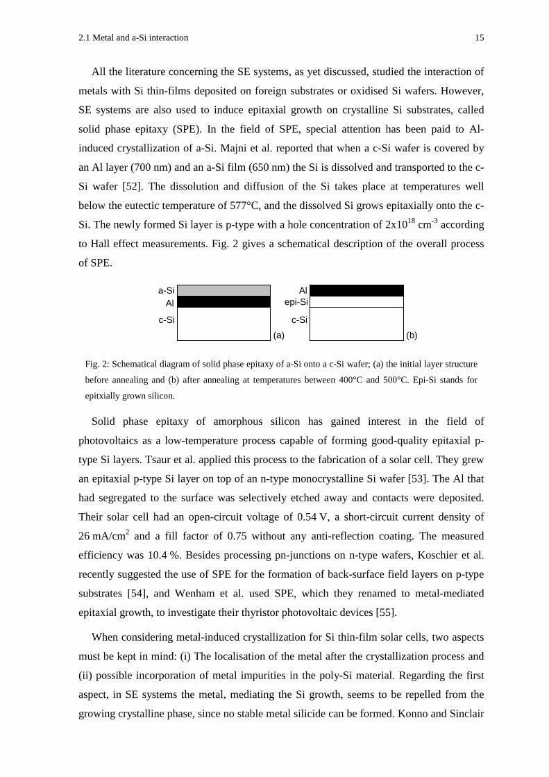
Si/metal systems. Table 1 lists some Si/metal systems with their eutectic temperatures Teu
and the reported crystallization temperatures Tcryst:
HX!"# FU\VW!"# $
Al 577 150 [34]
Ag 830 350 [35]
Au 360 130 [36]
Sb 630 430 [37]
Cu 802 485 [38]
Ni 964 500 [39]
Herd et al. have given a distinction between the different a-Si/metal systems [24]. On
one hand, there is the category of simple eutectic systems (SE systems) such as Al/Si,
Au/Si, or Ag/Si. Within these systems there is no formation of stable silicides in
thermodynamic equilibrium. However, metastable silicide transition phases might be
involved in the metal-induced crystallization (MIC) process [36,41]. The possible role of
an intermediate phase in Al-induced crystallization of a-Si will be discussed in chapter 6.1.
On the other hand, there is the category of compound forming metal/Si systems (CF
systems) such as Ni/Si, Pd/Si or Cu/Si. In these systems stable metal silicide phases exist
in thermal equilibrium and play an important role during the crystallization process. Both
categories will be discussed here. The emphasis will, however, be on the simple metal/Si
systems, since they are the most relevant for the work presented.
The following discussion will begin with the category of the compound forming
metal/Si systems, and will initially focus on Ni as the crystallization inducing metal,
because Ni has attracted the widest attention recently [25,26,39,42,43]. The interest in Ni-
induced crystallization is fuelled by the idea to replace the a-Si in thin-film transistors with
low-temperature poly-Si material for improved application in active-matrix liquid crystal
display devices. Ni seems to be a promising candidate to crystallize a-Si for use in this
field [25]. Hayzelden and Batstone have investigated Ni-induced crystallization by
studying the transformation of Ni-implanted amorphous Si [42,44], whilst Jin et al.
conducted research on Ni-covered a-Si thin-films [43]. In both cases it seems that the
fundamental crystallization process follows the same rules. In the initial phase of the
Table 1: List of Si/metal systems with their eutectic temperatures and crystallization temperatures reported.
All eutectic temperatures are taken from Ref. [40].
2.1 Metal and a-Si interaction 13
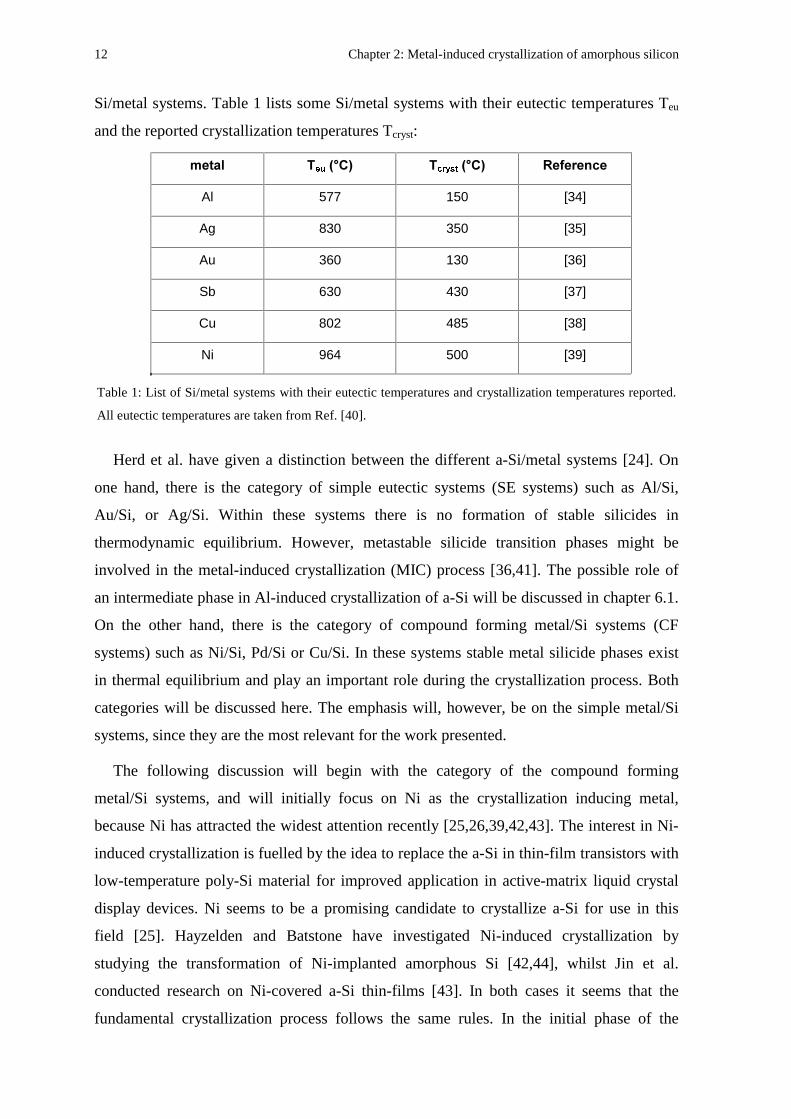
process, a metallic silicide, specifically NiSi2, is either formed at the Ni/a-Si interface, as in
the study of Jin et al., or as NiSi2 precipitates within the Ni-implanted a-Si material. The
NiSi2 precipitates migrate in the form of nodules through the amorphous silicon phase
leaving a trace of c-Si behind as schematically described in Fig. 1. The Ni-silicide is at the
planar growth front of the c-Si needle. Hayzelden and Batstone used a dissociation
mechanism to describe the growth process [42]. This mechanism is based on the fact that
the chemical potential of Ni is lower at the NiSi2/a-Si interface, whereas the chemical
potential of Si is lower at the NiSi2/c-Si interface. The NiSi2 layer dissociates at the Ni
silicide/c-Si interface to provide free silicon atoms for the Si crystal growth. Ni, enriched at
this interface, diffuses to the NiSi2/a-Si interface where new NiSi2 is formed.
Consequently, a net migration of the Ni silicide occurs transforming amorphous to
crystalline silicon, driven by the overall reduction of Gibbs energy.
If the above stated model for the Ni/Si system is generalised, it can be summarised that
in CF systems, it is not the metal itself that directly mediates the crystallization process. It
is a form of the metal silicide that induces the transformation of the amorphous to the
crystalline Si phase. Additionally, it is noteworthy that the individual Si atoms do not
strongly change their local position by long range diffusion, rather, their surrounding
changes. Initially, the Si atoms are incorporated in the amorphous Si matrix. During the
migration of the NiSi2 nodules the surrounding of the individual Si atom transforms to a Ni
silicide. Finally, the Si is released by the dissociation of the NiSi2 at the NiSi2/c-Si
interface and incorporated into the crystalline Si structure. The maximal relocation distance
of a Si atom is given by the possible diffusion length of the atom through the migrating Ni
silicide. The thickness of the planar NiSi2 growth front is stated as 5 nm [42].
Whilst the discussion of compound forming metal/Si systems was kept brief, the
following discussion on the category of simple eutectic systems has to be more in depth,
since the Al/Si system investigated in this work falls into this category. Herd et al. claimed
to have found a simple relationship between the eutectic melting temperature, Teu, and the
temperature of the on-set of the metal-induced crystallization of a-Si in SE systems [24].
c-Si a-SiNiSi2
Ni-atoms
Fig. 1: Schematical diagram of Ni-induced crystallization according to Refs. [42] and [43].
14 Chapter 2: Metal-induced crystallization of amorphous silicon
However, their rule that the crystallization temperature is 0.72 x Teu (Teu in Kelvin) is no
longer valid when more recent literature is considered (see Table 1). Nevertheless, the
crystallization process in SE systems seems to be of a common nature. The process can be
separated into three major steps: (i) the dissociation of Si atoms from the amorphous
silicon into the metal, (ii) the diffusion of the Si atoms through the metal, and (iii) the
incorporation of the dissolved Si atoms to the growing Si crystals. These Si crystals have
either nucleated at the Si/metal interface or within the metal itself, fed from the Si solute.
This simplified three step description of the crystallization process in SE systems was
adapted by Bian et al. to explain their findings on the formation of large Si grains (~1 µm)
in an a-Si/Ag/a-Si trilayer structure [35]. Tsai et al. could also explain the interfacial
reactions between Au and hydrogenated amorphous Si, observed in their investigation,
using this model [45]. Regarding the Al/Si system, Konno and Sinclair have conducted ex-
and in-situ cross-section transmission electron microscopy studies [46,47]. They gave
evidence that in an Al/a-Si multilayer structure heated to 200°C the formation of
crystalline Si nuclei occurs within the Al layers accompanied by the dissociation of the a-
Si layer. The results were interpreted as an indication that the Si atoms diffuse through the
Al to undergo the transition from the amorphous to the energetically more favourable
crystalline phase. The phenomenological dissociation-diffusion-crystallization model is
therefore supported by these studies.
So far, the discussion of the SE systems was limited to the transformation of amorphous
to crystalline silicon. However, metals of the SE systems also mediate the rearrangement
of polycrystalline silicon. Allen et al. studied the interaction of poly-Si in contact with Au
[48,49]. They showed that at temperatures below 300°C, initially large Si grains of the
polycrystalline material increase their size even further, at the expense of smaller grains.
The low temperature for the restructuring of the poly-Si material is due to an Au-mediated
process, according to Allen et al. The smaller Si grains are dissociated by the adjacent Au.
The dissolved Si atoms diffuse through the metal to the larger crystalline Si grains. Larger
grains are more stable due to a reduced ratio of Au/Si surface to crystalline volume.
Results, very similar to those for the Au/poly-Si system, have been reported for the
interaction of Al with poly-Si material [50,51]. The rearrangement of the Si films involves
the dissociation of Si into the Al and the diffusion of the Si atoms through the metal film.
These studies concerning the metal/poly-Si interaction also support the dissociation-
diffusion-crystallization model.
2.1 Metal and a-Si interaction 15
All the literature concerning the SE systems, as yet discussed, studied the interaction of
metals with Si thin-films deposited on foreign substrates or oxidised Si wafers. However,
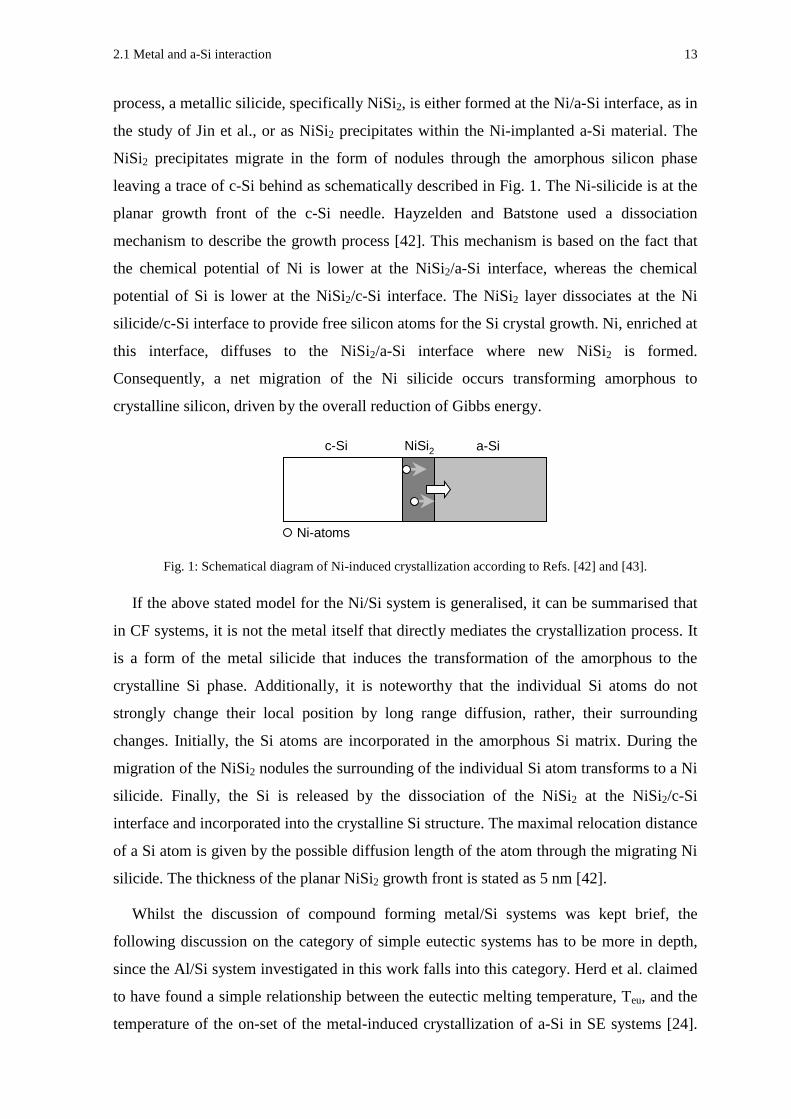
SE systems are also used to induce epitaxial growth on crystalline Si substrates, called
solid phase epitaxy (SPE). In the field of SPE, special attention has been paid to Al-
induced crystallization of a-Si. Majni et al. reported that when a c-Si wafer is covered by
an Al layer (700 nm) and an a-Si film (650 nm) the Si is dissolved and transported to the c-
Si wafer [52]. The dissolution and diffusion of the Si takes place at temperatures well
below the eutectic temperature of 577°C, and the dissolved Si grows epitaxially onto the c-
Si. The newly formed Si layer is p-type with a hole concentration of 2x1018 cm-3 according
to Hall effect measurements. Fig. 2 gives a schematical description of the overall process
of SPE.
Solid phase epitaxy of amorphous silicon has gained interest in the field of
photovoltaics as a low-temperature process capable of forming good-quality epitaxial p-
type Si layers. Tsaur et al. applied this process to the fabrication of a solar cell. They grew
an epitaxial p-type Si layer on top of an n-type monocrystalline Si wafer [53]. The Al that
had segregated to the surface was selectively etched away and contacts were deposited.
Their solar cell had an open-circuit voltage of 0.54 V, a short-circuit current density of
26 mA/cm2 and a fill factor of 0.75 without any anti-reflection coating. The measured
efficiency was 10.4 %. Besides processing pn-junctions on n-type wafers, Koschier et al.
recently suggested the use of SPE for the formation of back-surface field layers on p-type
substrates [54], and Wenham et al. used SPE, which they renamed to metal-mediated
epitaxial growth, to investigate their thyristor photovoltaic devices [55].
When considering metal-induced crystallization for Si thin-film solar cells, two aspects
must be kept in mind: (i) The localisation of the metal after the crystallization process and
(ii) possible incorporation of metal impurities in the poly-Si material. Regarding the first
aspect, in SE systems the metal, mediating the Si growth, seems to be repelled from the
growing crystalline phase, since no stable metal silicide can be formed. Konno and Sinclair
c-Si
a-SiAl
(a)
c-Si
epi-SiAl
(b)
Fig. 2: Schematical diagram of solid phase epitaxy of a-Si onto a c-Si wafer; (a) the initial layer structure
before annealing and (b) after annealing at temperatures between 400°C and 500°C. Epi-Si stands for
epitxially grown silicon.
16 Chapter 2: Metal-induced crystallization of amorphous silicon
have shown in TEM investigations that Al is ejected from its original position when the Si
nucleation and growth occurs within the Al layer [46]. A similar effect of metal
replacement has been discussed by Allen et al. in their study of the Au/poly-Si interaction
[48]. The solid solubility of the metal in the crystalline Si phase for Al and Au is about
10-2 at.% and 10-4 at.%, respectively [56], thus, in both cases very low. In contrast to SE
systems, the incorporation of metal silicide in the crystallized region cannot be excluded
when dealing with CF metal/Si systems. In respect to small devices, e.g. thin-film
transistors, the MIC process can be conducted in such a way that the residual NiSi2 phase
is extracted from the active device area [25]. However, for large-area devices, e.g. solar
cells, a localisation of areas harmful to the performance outside the active area does not
seem to be feasible. The use of SE systems to form poly-Si films is therefore more
promising with regard to photovoltaic applications.
When addressing the second aspect, i.e. the possible incorporation of metal atoms in the
poly-Si material, the energy levels of incorporated metal impurities in c-Si are of interest.
Ni as well as Au introduce deep states in the energy band gap of Si, whilst Al impurity
level is only about 60 meV above the valence band [57]. Deep states are harmful to the
photovoltaic performance of the device due to the enhanced Shockley-Read-Hall
recombination, which results form their presence. This means that Ni and Au seem to be
unsuitable as crystallization mediating metals when fabricating photovoltaic devices. By
comparison, the shallow impurity states caused by Al give rise to p-type doping when the
Al atoms occupy Si lattice sites (see chapter 5.3.). Incorporation of Al during the
aluminium-induced crystallization process could therefore be beneficial for subsequent
solar cell device fabrication depending on the solar cell structure, since p-type Si material
is automatically formed during the process.
From a photovoltaic point of view, a crystallization process, which transforms
amorphous silicon on low-cost substrates to poly-Si, is desired. The process requirements
are: (i) Low-temperatures, (ii) the formation of continuous high-quality Si layers over large
areas, and (iii) minimal potential of incorporating harmful impurities during the process.
The first requirement is generally fulfilled by metal-induced crystallization as described
above. It will be shown during this study that a layer exchange process based on
aluminium-induced crystallization is able to match the latter two requirements, as well.
The approach chosen is that Al and a-Si layers are subsequently deposited and a separate
isothermal annealing process is employed. During this annealing step an Al-induced layer
exchange occurs, which leads to the formation of a continuous poly-Si layer at low
2.1 Metal and a-Si interaction 17
temperatures on glass with a high crystallographic quality as documented in the following
chapters. This has not been achieved by metal-induced crystallization prior to this study to
the best of the author’s knowledge.
An attempt to give an overview on MIC investigations relevant to this work ought to
include approaches where Al induces crystallization already during the Si deposition.
Drüsedau et al. have studied the formation of polycrystalline Si when deposited onto Al
coated substrates at elevated temperatures [58,59]. The Al layers were between 4 and
32 nm thick. The subsequent deposition of 500 nm Si was conducted at a constant substrate
temperature of 227°C. The silicon layer crystallized during the deposition and contained Si
crystallites of about 10-30 nm in size. However, the Al is distributed in the crystallized
region of the film, and no pure continuous poly-Si layer is formed. Boreland et al. reported
similar difficulties in their studies on aluminium-induced crystal growth during chemical
vapour deposition of Si [28]. The average grain size of their Si thin-films was only about
70 nm, and the Si films still contained a substantial amount of Al.
%
The phenomenon investigated in this work is the aluminium-induced layer exchange
process (ALILE). In this process, adjacent aluminium and amorphous silicon layers
exchange places when heated at temperatures well below the eutectic temperature of the
Si/Al binary system. All experimental details will be described in chapter 3. At this point,
the key results and the basic parameters of this layer exchange are to be introduced, which
leads to an outline of the investigation and discussion of the process subsequently
presented.
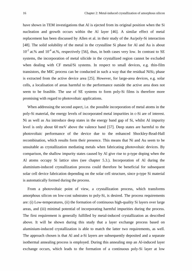
The overall Al-induced layer exchange phenomenon is shown in Fig. 3. The initial
system is a stacked Al and Si layer structure on glass. When this structure is heated, a layer
exchange process occurs. During the exchange, a polycrystalline silicon layer is formed at
the original position of the Al film. After selective removal of the Al that has segregated to
the top of the Si film, a continuous poly-Si layer remains on the glass substrate, as revealed
in Fig. 3c.
18 Chapter 2: Metal-induced crystallization of amorphous silicon
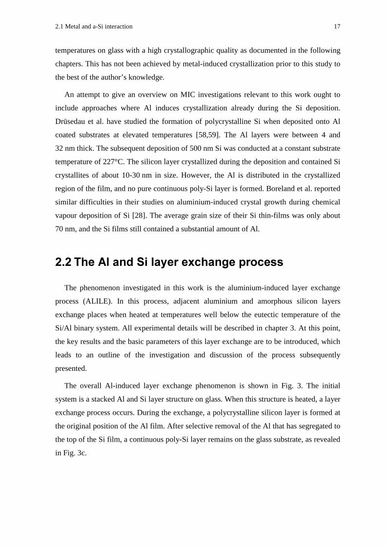
The crystalline nature of the Si layer after ALILE was verified using Raman
spectroscopy. Fig. 4 shows two spectra of a poly-Si layer on glass after crystallization.
They were taken from the surface as well as from the interface between the Si film and the
substrate, although the signal to noise ratio of the Raman signal detected through the glass
was decreased. The peak maxima of the spectra are at 520 cm-1. There is no Raman
response at 480 cm-1 that would indicate an amorphous phase in the Si material [16]. The
matching line shapes of the two peaks indicate that the crystalline character of the film is
uniform throughout the film thickness. To verify that the crystallization is induced by the
Al layer, an identical sample but without Al was subjected to the same annealing process.
It is apparent from Fig. 4 that this Si film remained amorphous. Thus, it is the Al layer that
is responsible for the transformation of an a-Si film into a poly-Si layer.
Fig. 3: Cross section FIB micrographs of the glass/Al/a-Si structure: (a) before annealing and (b) after
annealing for 1 h at 500°C. (c) SEM micrograph after Al etching, exposing the continuous poly-Si layer.
In (a) and (b) the samples are tilted by 45º, and in (c) the sample is tilted by 20º, therefore the scales are
only valid horizontally. The short white dotted line in (c) is a guide to the eye.
2.2 The Al and Si layer exchange process 19
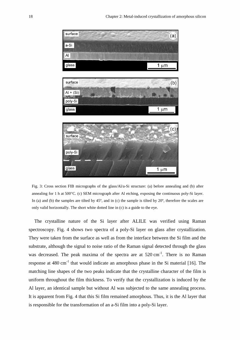
Raman measurements can also give a first impression of the good crystallographic
quality of the poly-Si material. Fig. 5 depicts two Raman spectra comparing
monocrystalline Si (c-Si) to poly-Si processed by ALILE. For better comparison each
spectrum is normalised to its peak maximum. The peak position of the poly-Si film is
identical to that for c-Si material indicating that the film is under no or negligible stress
[60]. The analysis of the Raman spectrum of the poly-Si layer reveals that the signal is
subject to greater noise than the comparative polished Si-wafer. This noise is due to higher
surface roughness. Subtracting the background noise in Fig. 5 leads to an almost complete
400 450 500 550 6000.0
0.5
1.0
poly-Si at surface
poly-Si at interface
samplewithoutAl layer
Nor
mal
ised
inte
nsity
[a.u
.]
Wavenumber [cm-1]
Fig. 4: Raman spectra of a sample annealed at 480°C for 45 min taken at the interface and the surface; the
spectrum of an identical sample having undergone the same annealing treatment but without Al is also
shown.
500 510 520 530 5400.0
0.5
1.0
poly-Sipoly-Si
c-Si
Nor
mal
ised
inte
nsity
Wavenumber [cm-1]
Fig. 5: Raman spectra of a crystallized sample and a polished crystalline Si wafer for comparison. Each
spectrum is normalised to its maximum. The Raman signal of the poly-Si film is subject to greater noise
due to higher surface roughness.
20 Chapter 2: Metal-induced crystallization of amorphous silicon
overlap of the two spectra taking into account the 1 cm-1 resolution of the Raman system.
There is no detectable broadening of the poly-Si peak on the lower energy side, which
would be caused by grain size and boundary effects [61]. Fauchet et al. pointed out that the
phonon spectrum is not just affected by the grain size but also by defects within the grains
[62]. Consequently, the Raman measurements give the first indication of the good
crystallographic properties of the poly-Si and the complete crystallization of the
amorphous material.
Since the key result of this study is the formation of continuous poly-Si films at low
temperatures by an Al-induced layer exchange process, the key questions investigated are:
Which process parameters influence the poly-Si formation? What are the properties of the
Si layer grown? How is the poly-Si film formed? Why does the layer exchange occur? The
work presented intends to provide answers to these questions. It is the isolated
investigations - where possible - of the various process parameters that lead to a picture of
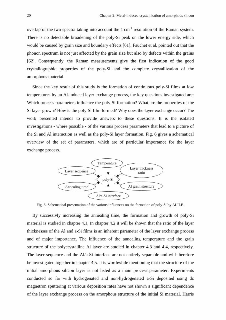
the Si and Al interaction as well as the poly-Si layer formation. Fig. 6 gives a schematical
overview of the set of parameters, which are of particular importance for the layer
exchange process.
By successivly increasing the annealing time, the formation and growth of poly-Si
material is studied in chapter 4.1. In chapter 4.2 it will be shown that the ratio of the layer
thicknesses of the Al and a-Si films is an inherent parameter of the layer exchange process
and of major importance. The influence of the annealing temperature and the grain
structure of the polycrystalline Al layer are studied in chapter 4.3 and 4.4, respectively.
The layer sequence and the Al/a-Si interface are not entirely separable and will therefore
be investigated together in chapter 4.5. It is worthwhile mentioning that the structure of the
initial amorphous silicon layer is not listed as a main process parameter. Experiments
conducted so far with hydrogenated and non-hydrogenated a-Si deposited using dc
magnetron sputtering at various deposition rates have not shown a significant dependence
of the layer exchange process on the amorphous structure of the initial Si material. Harris
Temperature
Al/a-Si interface
poly-Si
Al grain structure
Layer thicknessratioLayer sequence
Annealing time
Fig. 6: Schematical presentation of the various influences on the formation of poly-Si by ALILE.
2.2 The Al and Si layer exchange process 21
et al. made similar observations when they compared the interaction of Al with a-Si
deposited by electron-beam evaporation and chemical vapour deposition [50]. The
structure of the amorphous Si as a process parameter is therefore not discussed in a
separate chapter. The study of the ALILE process in conjunction with the analysis of the
material properties of the poly-Si films are the basis of a model describing this layer
exchange process, which is developed in chapter 6.

23
&
'
This chapter on the preparation and characterisation techniques is kept short, because
the standard deposition methods used in this work were conventional sputtering deposition
and thermal evaporation. The characterisation methods applied were mainly common
electron microscopy and spectroscopy techniques. Brief descriptions will only be given for
more “exotic” methods, such as focused ion beam and orientation imaging microscopy.
Their particular relevance to the research on ALILE will become apparent when these
techniques are discussed in the course of the presentation of specific measurements.
&(
The aluminium and amorphous silicon layers were deposited onto glass. The type of
glass substrate used was Corning 1737F. This alkaline earth aluminosilicate glass is
superior to other commonly used glass substrates such as barium borosilcicate glass
(Corning 7059). The reason is that its thermal expansion coefficient (3.8x10⁻⁶°C-1) matches
better to the one of silicon (2.6x10⁻⁶°C-1) compared to borosilicate glass substrates
(4.7x10⁻⁶°C-1).* An additional general advantage of the chosen substrate type is its higher
strain point of 666 °C compared to 400-600°C of conventional glass.
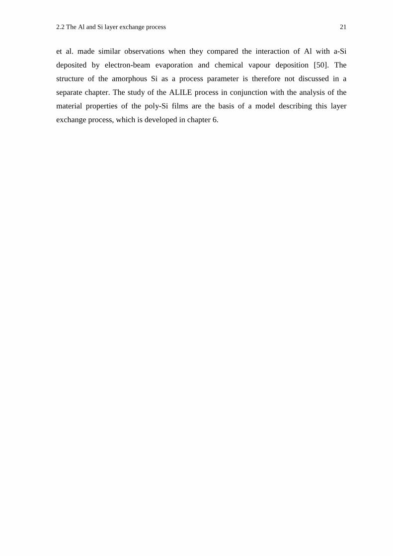
Another important piece of information about the substrate is the material composition
contained in the glass. Table 2 gives the molecular fractions of compounds of which the
glass consists. These fractions given by the manufacturer can be converted to weight and
atomic fractions of the individual elements as shown in table 3.
Before any deposition was carried out, the glass substrates were cleaned using RCA1
and an HF dip (dilute HF of about 2%) [63]. The clean substrates were immediately loaded
* All material properties stated are extracted from the product information sheet for Corning glass 1737F
available for example from Corning International Corporation Australia.
24 Chapter 3: Experimental
into the deposition chambers to deposit various Al and a-Si layer sequences. Generally, the
Al film was deposited using thermal evaporation. Prior to the evaporation the chamber was
pumped down to 7x10⁻⁴ Pa. The following deposition was conducted at rates ranging from
0.5 to 10 nm/s. The amorphous silicon was deposited using dc magnetron sputtering at a
rate of 25 nm/min in a 1.5 Pa argon atmosphere at 100 W after the base pressure read
below 2.4x10⁻⁴ Pa. A 100 mm, 120 Ωcm boron doped Czochralski-Si wafer was used as
the sputtering target. No substrate heating was employed in either thermal evaporation or
sputtering deposition. It has to be noted that the samples were exposed to air during the
transfer from one deposition chamber to the other.
The thermal annealing process of the Al and a-Si layer structure was conducted at
temperatures ranging from 350°C to 525ºC for annealing times from 5 min to 60 h. The
heat treatment was mainly performed in a furnace with dry N2 ambient. It was interrupted
by removing the samples from the furnace and cooling them to below 100ºC in less than
2 min in a strong N2 flow. The only exception to this annealing procedure was during time
dependent crystallization studies under an optical microscope, which was equipped with a
heat stage. The stage could be heated up to the final temperature within 5 min in ambient
air. However, within the temperature range investigated, an error of ±25ºC had to be
allowed for temperature inhomogeneity within the stage.
- 0 - 0 0
SiO2 55 to 59 O 49,3 62,2
Al2O3 16 to 18 Si 26,6 19
BaO 7 to 9 Al 9,0 6,8
B2O3 7 to 9 Ba 7,2 4
CaO 4 to 6 B 1,2 3,2
MgO 0.5 to 1 Ca 3,6 2,5
SrO 1 to 2 Mg 0,6 0,5
As2O3 1 to 2 Sr 1,7 1
As 0,8 0,8
Table 2: Molecular fraction in Corning 1737 Table 3: Weight and atomic fractions of the elements
contained in Corning 1737
3.1 Preparation 25
To investigate the bare poly-Si layer formed during annealing, the Al that had
precipitated on the surface during the process was selectively etched off using a standard
Al etching solution (80 parts phosphoric acid, 5 parts nitric acid, 5 parts acetic acid, and 10
parts deionized water at 50°C to 55°C).
&
The aluminium-induced layer exchange process at temperatures below the eutectic
temperature was studied using several microscopical, spectroscopical and electrical
techniques. Although most of these techniques are standard characterisation techniques for
semiconductor and material research, some specific advantages of the less common ones
will be mentioned in the following exposition.
To investigate the interaction of the Al and a-Si layers optical microscopy, scanning
electron microscopy (SEM), Hitachi S900 and S4500 equipped with an energy-
dispersive x-ray spectrometer (EDS), Oxford Link ISIS 200 Microanalysis System and
focused ion beam microscopy (FIB), FEI FIB200xP, were employed. The FIB can be
exceptionally useful to study the diffusive interaction of layered metal and semiconductor
structures. Firstly, the Ga+ beam of the FIB allows milling of clean cross sections as well
as imaging (see for example Olson et al. for more details on FIB microscopy [64]).
Secondly, due to the FIB’s high voltage contrast between metallic and non-metallic
materials, areas of Al and Si can clearly be distinguished. The relationship between the
voltage contrast and the type of material was verified by cross sectional energy-dispersive
x-ray spectroscopy.
To study the crystallographic structure of the polycrystalline silicon films transmission
electron microscopy (TEM), Philips CM200 and orientation imaging microscopy
(OIM), TexSEM were used. The OIM captures and analyses the backscattered Kikuchi
diffraction pattern (BKD) generated by the crystalline material [65]. The BKD is generated
in a SEM set-up and reveals the lattice orientation in the microstructure. Thus, the analysis
of the BKDs over an entire region allows to determine grain orientation as well as grain
boundaries (GBs) due to the difference of lattice orientation from one side of the grain
boundary to the other. The boundary level of the OIM is set to 5° in all measurements
presented. The application of an OIM for investigating polycrystalline material will be
discussed in chapter 5.2 using orientation imaging micrographs for better explanation. The
26 Chapter 3: Experimental
OIM studies of the poly-Si grain structure were complemented by utilising the electron
channelling contrast of a conventional SEM. This technique enabled the investigation of
larger areas of the fully crystallized poly-Si layers than commonly possible in TEM
studies. The electron channelling images were made from the former glass/poly-Si
interface after lifting the Si films off the glass substrate with concentrated HF. The
separated poly-Si layers were turned upside-down and transferred onto metal substrates.
This preparation ensured a smooth, clean surface. A secondary electron detector positioned
below the objective lens of the SEM recorded a signal with a strong channelling contrast
due to sensitivity of the electron backscattering coefficient to the crystallographic
orientation of the Si grains [66].
As a standard measurement for the crystallographic quality of poly-Si layer, Raman
Spectroscopy (Renishaw Ramascope equipped with a HeNe-Laser, wavelength 632.8 nm)
was used. It was separately tested that the laser beam did not induce any crystallization in
a-Si films on glass even after extended periods of exposure (>1 h). X-ray diffraction
measurements were employed to investigate the orientation of the Si grains of the
polycrystalline material. X-ray diffractograms of the poly-Si films were measured in
symmetric θ−2θ geometry. A Bruker D8 Advance diffractometer was used which was
equipped with a Göbel mirror for parallel beam diffraction [67] and operated with CuKα
radiation (λα1 = 1.5406 Å). In order to obtain a reliable signal-to-noise ratio within a finite
measurement time, a position sensitive detector (PSD), Braun was used to record the
Bragg reflections in the fixed PSD mode. For this purpose the centre of the PSD was set to
the scattering angle 2θ0 of the reflection under consideration, while the tube was positioned
at θ0. Prior to the measurements of poly-Si films the PSD mode was verified for a quartz
standard sample to yield the same relative intensities as in the usual locked-coupled mode
for which both the X-ray tube and the PSD are step-wise moved along the θ and 2θ circle,
respectively.
The Al quantities remaining in the crystallized silicon were detected using secondary
ion mass spectroscopy (SIMS); whilst the Si-O and Al-O compound distribution before
and after the layer exchange process was qualitatively investigated with x-ray
photoelectron spectroscopy (XPS). The XPS analysis involved the usage of a VG
ESCALAB 220i XL surface science instrument that was equipped with a monochromated
Al Kα1 X-ray source (the analyser pass energy was set to 20 eV). The ion bombardment
for depth profiling involved a scanning Ar+ ion gun, which was operated at an energy of
3.2 Characterisation 27
3 keV. The electrical measurements were based on four-point probe as well as resistivity
and Hall-effect measurements that were conducted on 25 mm2 squares of film, with Al
dots fabricated on the corners using the Van der Pauw technique.

29
)
(%
The investigations presented in this chapter focus on the parameters of the metal-
induced Al and Si layer exchange process. They target the question: In what way do which
parameters influence the formation of the poly-Si material? Firstly, the time dependent Si
grain growth and formation of a poly-Si layer by ALILE is analysed. The subsequent
studies concentrate on influences of the layer thickness ratio of the adjacent Al and a-Si
films, the annealing temperature, the structure of the polycrystalline Al and the Al/Si
interface.
) *
The default structure to investigate the formation of poly-Si by ALILE was a glass
substrate covered by one layer of Al and one layer of a-Si. The layers were of almost equal
thicknesses (400 nm Al and 500 nm a-Si). The interaction of these two films was studied in
various ways. Firstly, the duration of the annealing time for the crystallization process was
varied from 5 min to 60 h at different temperatures. To investigate the interaction of the a-
Si and Al layers in the glass/Al/a-Si structure, cross-sections of the samples were prepared
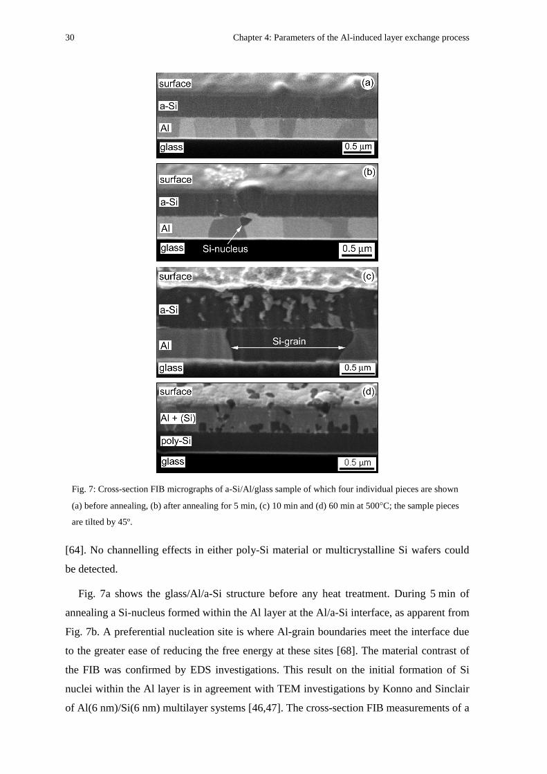
and imaged using FIB. Fig. 7 depicts a series of samples before and after annealing at
500ºC for 5 min, 10 min, and 60 min. All samples were prepared in the same thermal
evaporation and sputtering process to ensure identical conditions prior to annealing. The Al
layers in images Fig. 7a and Fig. 7b show slight grey variations within the layer. These
variations were caused by the channelling behaviour of the ion beam during imaging. The
ions penetrate into the polycrystalline Al to different depths according to the
crystallographic orientation of the Al grains, consequently, giving rise to variations in
secondary electrons generated. This effect is particularly prevalent in polycrystalline Al
30 Chapter 4: Parameters of the Al-induced layer exchange process
[64]. No channelling effects in either poly-Si material or multicrystalline Si wafers could
be detected.
Fig. 7a shows the glass/Al/a-Si structure before any heat treatment. During 5 min of
annealing a Si-nucleus formed within the Al layer at the Al/a-Si interface, as apparent from
Fig. 7b. A preferential nucleation site is where Al-grain boundaries meet the interface due
to the greater ease of reducing the free energy at these sites [68]. The material contrast of
the FIB was confirmed by EDS investigations. This result on the initial formation of Si
nuclei within the Al layer is in agreement with TEM investigations by Konno and Sinclair
of Al(6 nm)/Si(6 nm) multilayer systems [46,47]. The cross-section FIB measurements of a
Fig. 7: Cross-section FIB micrographs of a-Si/Al/glass sample of which four individual pieces are shown
(a) before annealing, (b) after annealing for 5 min, (c) 10 min and (d) 60 min at 500°C; the sample pieces
are tilted by 45º.
4.1 Si grain formation and growth 31
sample annealed for 10 min (Fig. 7c) shows that the Si nuclei grew into the Al layer until
they were confined between the Al/a-Si interface and the glass substrate. Sandwiched
between these two boundaries the grains continued to grow laterally. The crystal growth
terminated when adjacent grains impinged, finally forming a continuous polycrystalline
silicon film on the substrate (Fig. 7d). During the poly-Si growth the Al segregated to the
top of the sample. Si material, which was not incorporated into the poly-Si layer, formed
small Si crystals within the newly evolved Al layer. These crystals are observed as dark
areas in the Al layer in Fig. 7d. The overall process during the Si and Al layer interaction
leads to an exchange of layer positions leaving the poly-Si film on the glass with the Al
layer on top.
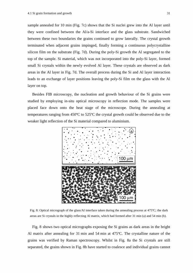
Besides FIB microscopy, the nucleation and growth behaviour of the Si grains were
studied by employing in-situ optical microscopy in reflection mode. The samples were
placed face down onto the heat stage of the microscope. During the annealing at
temperatures ranging from 450ºC to 525ºC the crystal growth could be observed due to the
weaker light reflection of the Si material compared to aluminium.
Fig. 8 shows two optical micrographs exposing the Si grains as dark areas in the bright
Al matrix after annealing for 31 min and 54 min at 475ºC. The crystalline nature of the
grains was verified by Raman spectroscopy. Whilst in Fig. 8a the Si crystals are still
separated, the grains shown in Fig. 8b have started to coalesce and individual grains cannot
a
b
Fig. 8: Optical micrograph of the glass/Al interface taken during the annealing process at 475ºC; the dark
areas are Si crystals in the highly reflecting Al matrix, which had formed after 31 min (a) and 54 min (b).
32 Chapter 4: Parameters of the Al-induced layer exchange process
easily be distinguished anymore. The advantage of in-situ optical microscopy
investigations lies in the opportunity of capturing images in film-like sequences directly
during the annealing process. From these sequences the growth of individual grains can be
observed and a clear distinction between separate grains and areas of coalesced grains is
possible. To study the evolution of the grain size distribution, only images taken before
significant coalescence occurred were taken into account. Due to the limited resolution of
the microscopy system, grains with a diameter smaller than 1 µm could not be detected.
The images were analysed by using the software package Image Tool (developed by the
University of Texas, Health Science Center in San Antonio, Texas). Since the Si grain
sizes exceed the layer thickness many times, the grain size distribution can be reduced to a
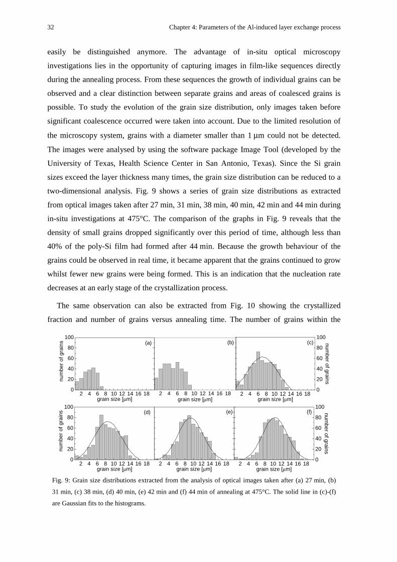
two-dimensional analysis. Fig. 9 shows a series of grain size distributions as extracted
from optical images taken after 27 min, 31 min, 38 min, 40 min, 42 min and 44 min during
in-situ investigations at 475°C. The comparison of the graphs in Fig. 9 reveals that the
density of small grains dropped significantly over this period of time, although less than
40% of the poly-Si film had formed after 44 min. Because the growth behaviour of the
grains could be observed in real time, it became apparent that the grains continued to grow
whilst fewer new grains were being formed. This is an indication that the nucleation rate
decreases at an early stage of the crystallization process.
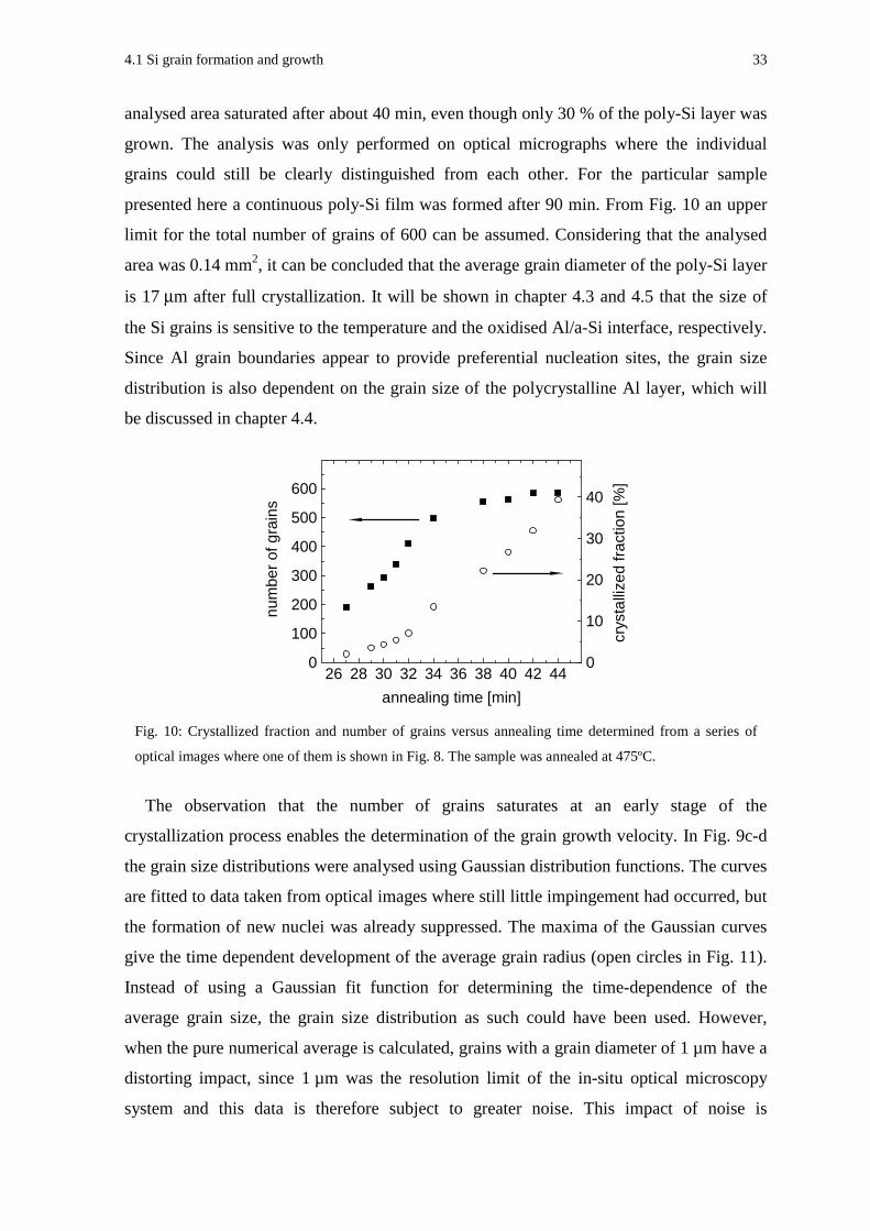
The same observation can also be extracted from Fig. 10 showing the crystallized
fraction and number of grains versus annealing time. The number of grains within the
2 4 6 8 10 12 14 16 180
20
40
60
80
100
num
ber
of g
rain
s
grain size [µm]2 4 6 8 10 12 14 16 18
0
20
40
60
80
100 number of grains
grain size [µm]2 4 6 8 10 12 14 16 18
grain size [µm]
2 4 6 8 10 12 14 16 180
20
40
60
80
100
num
ber
of g
rain
s
grain size [µm]2 4 6 8 10 12 14 16 18
0
20
40
60
80
100(f) num
ber of grains
grain size [µm]2 4 6 8 10 12 14 16 18
grain size [µm]
(a) (b) (c)
(d) (e) (f)
Fig. 9: Grain size distributions extracted from the analysis of optical images taken after (a) 27 min, (b)
31 min, (c) 38 min, (d) 40 min, (e) 42 min and (f) 44 min of annealing at 475°C. The solid line in (c)-(f)
are Gaussian fits to the histograms.
4.1 Si grain formation and growth 33
analysed area saturated after about 40 min, even though only 30 % of the poly-Si layer was
grown. The analysis was only performed on optical micrographs where the individual
grains could still be clearly distinguished from each other. For the particular sample
presented here a continuous poly-Si film was formed after 90 min. From Fig. 10 an upper
limit for the total number of grains of 600 can be assumed. Considering that the analysed
area was 0.14 mm2, it can be concluded that the average grain diameter of the poly-Si layer
is 17 µm after full crystallization. It will be shown in chapter 4.3 and 4.5 that the size of
the Si grains is sensitive to the temperature and the oxidised Al/a-Si interface, respectively.
Since Al grain boundaries appear to provide preferential nucleation sites, the grain size
distribution is also dependent on the grain size of the polycrystalline Al layer, which will
be discussed in chapter 4.4.
The observation that the number of grains saturates at an early stage of the
crystallization process enables the determination of the grain growth velocity. In Fig. 9c-d
the grain size distributions were analysed using Gaussian distribution functions. The curves
are fitted to data taken from optical images where still little impingement had occurred, but
the formation of new nuclei was already suppressed. The maxima of the Gaussian curves
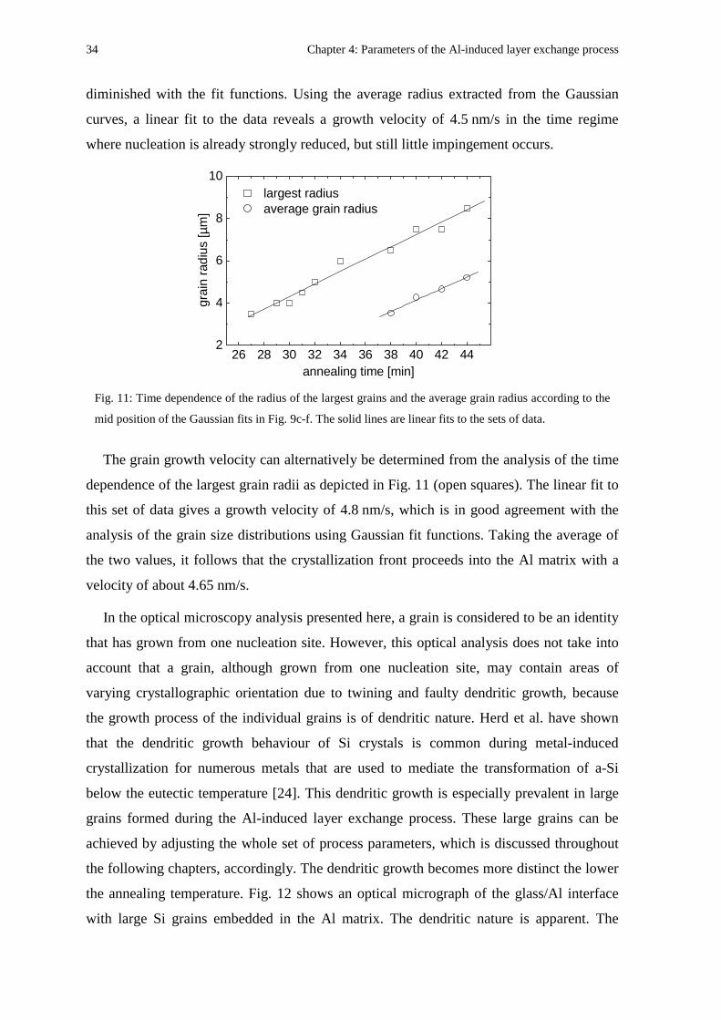
give the time dependent development of the average grain radius (open circles in Fig. 11).
Instead of using a Gaussian fit function for determining the time-dependence of the
average grain size, the grain size distribution as such could have been used. However,
when the pure numerical average is calculated, grains with a grain diameter of 1 µm have a
distorting impact, since 1 µm was the resolution limit of the in-situ optical microscopy
system and this data is therefore subject to greater noise. This impact of noise is
26 28 30 32 34 36 38 40 42 440
100
200
300
400
500
600
num
ber
of g
rain
s
annealing time [min]
0
10
20
30
40
crys
talli
zed
frac
tion
[%]
Fig. 10: Crystallized fraction and number of grains versus annealing time determined from a series of
optical images where one of them is shown in Fig. 8. The sample was annealed at 475ºC.
34 Chapter 4: Parameters of the Al-induced layer exchange process
diminished with the fit functions. Using the average radius extracted from the Gaussian
curves, a linear fit to the data reveals a growth velocity of 4.5 nm/s in the time regime
where nucleation is already strongly reduced, but still little impingement occurs.
The grain growth velocity can alternatively be determined from the analysis of the time
dependence of the largest grain radii as depicted in Fig. 11 (open squares). The linear fit to
this set of data gives a growth velocity of 4.8 nm/s, which is in good agreement with the
analysis of the grain size distributions using Gaussian fit functions. Taking the average of
the two values, it follows that the crystallization front proceeds into the Al matrix with a
velocity of about 4.65 nm/s.
In the optical microscopy analysis presented here, a grain is considered to be an identity
that has grown from one nucleation site. However, this optical analysis does not take into
account that a grain, although grown from one nucleation site, may contain areas of
varying crystallographic orientation due to twining and faulty dendritic growth, because
the growth process of the individual grains is of dendritic nature. Herd et al. have shown
that the dendritic growth behaviour of Si crystals is common during metal-induced
crystallization for numerous metals that are used to mediate the transformation of a-Si
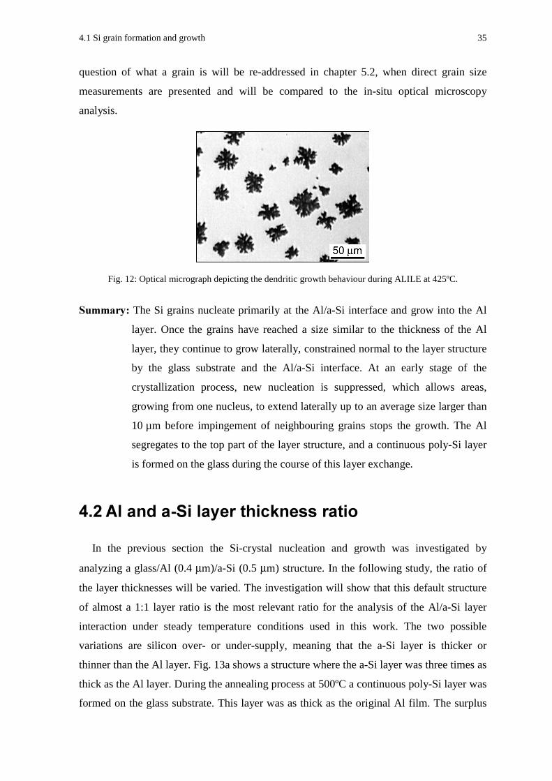
below the eutectic temperature [24]. This dendritic growth is especially prevalent in large
grains formed during the Al-induced layer exchange process. These large grains can be
achieved by adjusting the whole set of process parameters, which is discussed throughout
the following chapters, accordingly. The dendritic growth becomes more distinct the lower
the annealing temperature. Fig. 12 shows an optical micrograph of the glass/Al interface
with large Si grains embedded in the Al matrix. The dendritic nature is apparent. The
26 28 30 32 34 36 38 40 42 442
4
6
8
10
grai
n ra
dius
[µm
]
annealing time [min]
largest radiusaverage grain radius
Fig. 11: Time dependence of the radius of the largest grains and the average grain radius according to the
mid position of the Gaussian fits in Fig. 9c-f. The solid lines are linear fits to the sets of data.
4.1 Si grain formation and growth 35
question of what a grain is will be re-addressed in chapter 5.2, when direct grain size
measurements are presented and will be compared to the in-situ optical microscopy
analysis.
' The Si grains nucleate primarily at the Al/a-Si interface and grow into the Al
layer. Once the grains have reached a size similar to the thickness of the Al
layer, they continue to grow laterally, constrained normal to the layer structure
by the glass substrate and the Al/a-Si interface. At an early stage of the
crystallization process, new nucleation is suppressed, which allows areas,
growing from one nucleus, to extend laterally up to an average size larger than
10 µm before impingement of neighbouring grains stops the growth. The Al
segregates to the top part of the layer structure, and a continuous poly-Si layer
is formed on the glass during the course of this layer exchange.
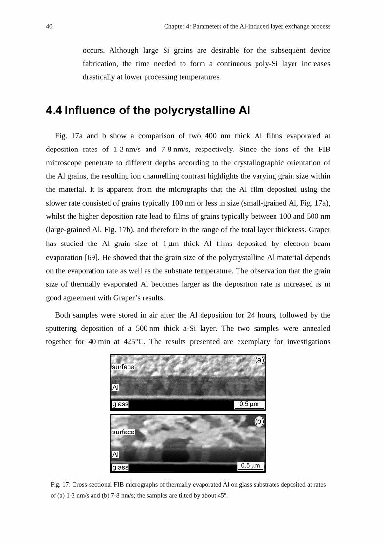
)% +
In the previous section the Si-crystal nucleation and growth was investigated by
analyzing a glass/Al (0.4 µm)/a-Si (0.5 µm) structure. In the following study, the ratio of
the layer thicknesses will be varied. The investigation will show that this default structure
of almost a 1:1 layer ratio is the most relevant ratio for the analysis of the Al/a-Si layer
interaction under steady temperature conditions used in this work. The two possible
variations are silicon over- or under-supply, meaning that the a-Si layer is thicker or
thinner than the Al layer. Fig. 13a shows a structure where the a-Si layer was three times as
thick as the Al layer. During the annealing process at 500ºC a continuous poly-Si layer was
formed on the glass substrate. This layer was as thick as the original Al film. The surplus
Fig. 12: Optical micrograph depicting the dendritic growth behaviour during ALILE at 425ºC.
36 Chapter 4: Parameters of the Al-induced layer exchange process
of Si material resulted in the formation of a Si network, visible after Al etching as depicted
in Fig. 13b. The crystalline nature of the Si network was verified using Raman
spectroscopy.
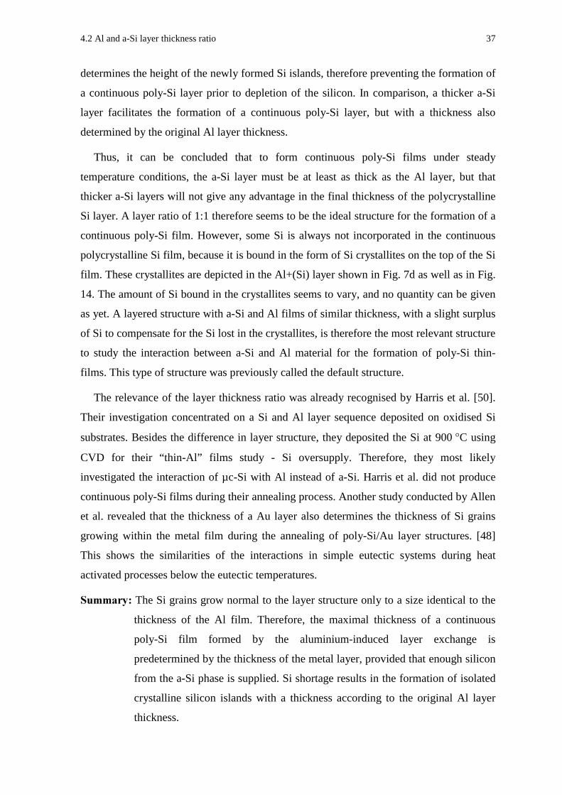
If the Si layer is thinner than the Al layer, scarcity of Si material occurs and therefore no
continuous poly-Si film can be formed. However, isolated islands of crystalline silicon
grow. These islands have the thickness of the original Al layer and vary in size depending
on the Si supply. In Fig. 14 a sample is shown where the initial a-Si layer was only half the
thickness of the 0.5 µm thick Al layer. After annealing at 500ºC and Al etching, Si islands
were visible in SEM studies. Additionally, Si crystals were formed in the top layer and can
be seen as protrusions on top of the Si islands. The Si bound in these crystals is lost for Si
grain growth within the former Al layer.
Both cases indicated the importance of the Al/a-Si interface. As highlighted in the
previous paragraph, once the Si grains have grown to a thickness equal to that of the Al
film, further growth is confined to the space bounded by the substrate and the interface
between the two layers. In the case of Si shortage, the original metal layer thickness still
Fig. 13: Cross-section SEM micrographs showing (a) a specimen with a thicker a-Si than the Al layer
before heat treatment, (b) the same specimen after crystallization at 500°C and Al etching. The short
white dotted line in (b) is a guide to the eye.
former Al thickness
former a-Si thickness
Fig. 14: Cross-section SEM micrograph of a specimen after crystallization at 500°C and Al etching where
the original a-Si layer was only half the thickness of the Al layer.
4.2 Al and a-Si layer thickness ratio 37
determines the height of the newly formed Si islands, therefore preventing the formation of
a continuous poly-Si layer prior to depletion of the silicon. In comparison, a thicker a-Si
layer facilitates the formation of a continuous poly-Si layer, but with a thickness also
determined by the original Al layer thickness.
Thus, it can be concluded that to form continuous poly-Si films under steady
temperature conditions, the a-Si layer must be at least as thick as the Al layer, but that
thicker a-Si layers will not give any advantage in the final thickness of the polycrystalline
Si layer. A layer ratio of 1:1 therefore seems to be the ideal structure for the formation of a
continuous poly-Si film. However, some Si is always not incorporated in the continuous
polycrystalline Si film, because it is bound in the form of Si crystallites on the top of the Si
film. These crystallites are depicted in the Al+(Si) layer shown in Fig. 7d as well as in Fig.
14. The amount of Si bound in the crystallites seems to vary, and no quantity can be given
as yet. A layered structure with a-Si and Al films of similar thickness, with a slight surplus
of Si to compensate for the Si lost in the crystallites, is therefore the most relevant structure
to study the interaction between a-Si and Al material for the formation of poly-Si thin-
films. This type of structure was previously called the default structure.
The relevance of the layer thickness ratio was already recognised by Harris et al. [50].
Their investigation concentrated on a Si and Al layer sequence deposited on oxidised Si
substrates. Besides the difference in layer structure, they deposited the Si at 900 °C using
CVD for their “thin-Al” films study - Si oversupply. Therefore, they most likely
investigated the interaction of µc-Si with Al instead of a-Si. Harris et al. did not produce
continuous poly-Si films during their annealing process. Another study conducted by Allen
et al. revealed that the thickness of a Au layer also determines the thickness of Si grains
growing within the metal film during the annealing of poly-Si/Au layer structures. [48]
This shows the similarities of the interactions in simple eutectic systems during heat
activated processes below the eutectic temperatures.
' The Si grains grow normal to the layer structure only to a size identical to the
thickness of the Al film. Therefore, the maximal thickness of a continuous
poly-Si film formed by the aluminium-induced layer exchange is
predetermined by the thickness of the metal layer, provided that enough silicon
from the a-Si phase is supplied. Si shortage results in the formation of isolated
crystalline silicon islands with a thickness according to the original Al layer
thickness.
38 Chapter 4: Parameters of the Al-induced layer exchange process
)&
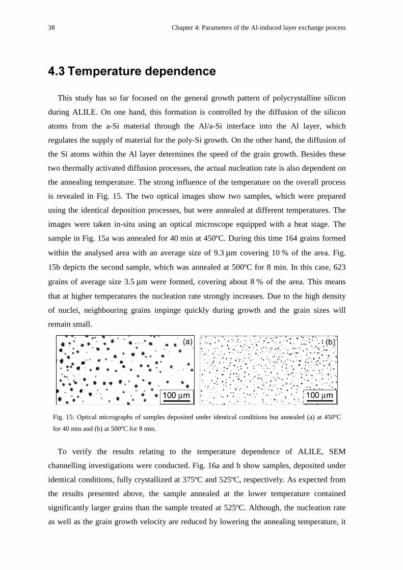
This study has so far focused on the general growth pattern of polycrystalline silicon
during ALILE. On one hand, this formation is controlled by the diffusion of the silicon
atoms from the a-Si material through the Al/a-Si interface into the Al layer, which
regulates the supply of material for the poly-Si growth. On the other hand, the diffusion of
the Si atoms within the Al layer determines the speed of the grain growth. Besides these
two thermally activated diffusion processes, the actual nucleation rate is also dependent on
the annealing temperature. The strong influence of the temperature on the overall process
is revealed in Fig. 15. The two optical images show two samples, which were prepared
using the identical deposition processes, but were annealed at different temperatures. The
images were taken in-situ using an optical microscope equipped with a heat stage. The
sample in Fig. 15a was annealed for 40 min at 450ºC. During this time 164 grains formed
within the analysed area with an average size of 9.3 µm covering 10 % of the area. Fig.
15b depicts the second sample, which was annealed at 500ºC for 8 min. In this case, 623
grains of average size 3.5 µm were formed, covering about 8 % of the area. This means
that at higher temperatures the nucleation rate strongly increases. Due to the high density
of nuclei, neighbouring grains impinge quickly during growth and the grain sizes will
remain small.
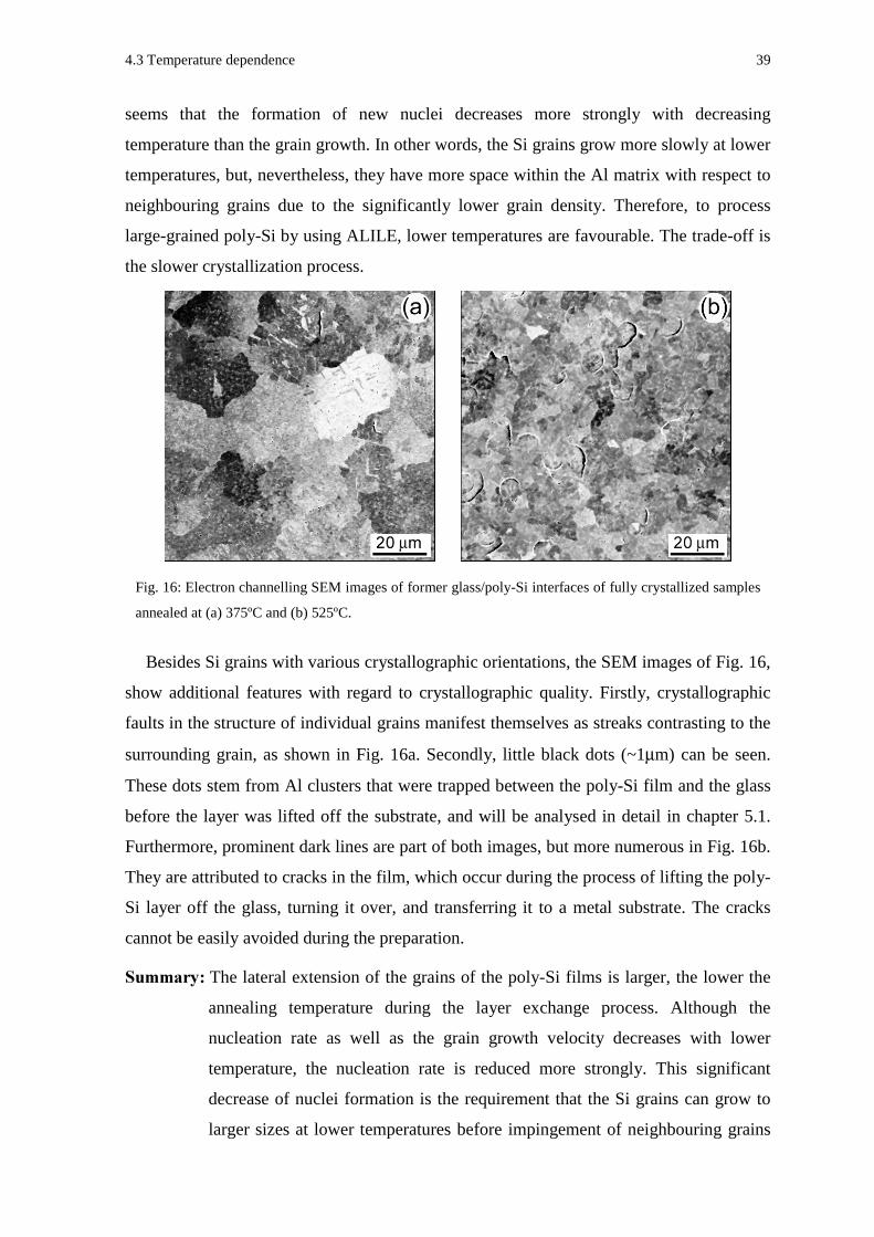
To verify the results relating to the temperature dependence of ALILE, SEM
channelling investigations were conducted. Fig. 16a and b show samples, deposited under
identical conditions, fully crystallized at 375ºC and 525ºC, respectively. As expected from
the results presented above, the sample annealed at the lower temperature contained
significantly larger grains than the sample treated at 525ºC. Although, the nucleation rate
as well as the grain growth velocity are reduced by lowering the annealing temperature, it
Fig. 15: Optical micrographs of samples deposited under identical conditions but annealed (a) at 450ºC
for 40 min and (b) at 500ºC for 8 min.
4.3 Temperature dependence 39
seems that the formation of new nuclei decreases more strongly with decreasing
temperature than the grain growth. In other words, the Si grains grow more slowly at lower
temperatures, but, nevertheless, they have more space within the Al matrix with respect to
neighbouring grains due to the significantly lower grain density. Therefore, to process
large-grained poly-Si by using ALILE, lower temperatures are favourable. The trade-off is
the slower crystallization process.
Besides Si grains with various crystallographic orientations, the SEM images of Fig. 16,
show additional features with regard to crystallographic quality. Firstly, crystallographic
faults in the structure of individual grains manifest themselves as streaks contrasting to the
surrounding grain, as shown in Fig. 16a. Secondly, little black dots (~1µm) can be seen.
These dots stem from Al clusters that were trapped between the poly-Si film and the glass
before the layer was lifted off the substrate, and will be analysed in detail in chapter 5.1.
Furthermore, prominent dark lines are part of both images, but more numerous in Fig. 16b.
They are attributed to cracks in the film, which occur during the process of lifting the poly-
Si layer off the glass, turning it over, and transferring it to a metal substrate. The cracks
cannot be easily avoided during the preparation.
'The lateral extension of the grains of the poly-Si films is larger, the lower the
annealing temperature during the layer exchange process. Although the
nucleation rate as well as the grain growth velocity decreases with lower
temperature, the nucleation rate is reduced more strongly. This significant
decrease of nuclei formation is the requirement that the Si grains can grow to
larger sizes at lower temperatures before impingement of neighbouring grains
Fig. 16: Electron channelling SEM images of former glass/poly-Si interfaces of fully crystallized samples
annealed at (a) 375ºC and (b) 525ºC.
40 Chapter 4: Parameters of the Al-induced layer exchange process
occurs. Although large Si grains are desirable for the subsequent device
fabrication, the time needed to form a continuous poly-Si layer increases
drastically at lower processing temperatures.
)) %
Fig. 17a and b show a comparison of two 400 nm thick Al films evaporated at
deposition rates of 1-2 nm/s and 7-8 nm/s, respectively. Since the ions of the FIB
microscope penetrate to different depths according to the crystallographic orientation of
the Al grains, the resulting ion channelling contrast highlights the varying grain size within
the material. It is apparent from the micrographs that the Al film deposited using the
slower rate consisted of grains typically 100 nm or less in size (small-grained Al, Fig. 17a),
whilst the higher deposition rate lead to films of grains typically between 100 and 500 nm
(large-grained Al, Fig. 17b), and therefore in the range of the total layer thickness. Graper
has studied the Al grain size of 1 µm thick Al films deposited by electron beam
evaporation [69]. He showed that the grain size of the polycrystalline Al material depends
on the evaporation rate as well as the substrate temperature. The observation that the grain
size of thermally evaporated Al becomes larger as the deposition rate is increased is in
good agreement with Graper’s results.
Both samples were stored in air after the Al deposition for 24 hours, followed by the
sputtering deposition of a 500 nm thick a-Si layer. The two samples were annealed
together for 40 min at 425°C. The results presented are exemplary for investigations
Fig. 17: Cross-sectional FIB micrographs of thermally evaporated Al on glass substrates deposited at rates
of (a) 1-2 nm/s and (b) 7-8 nm/s; the samples are tilted by about 45º.
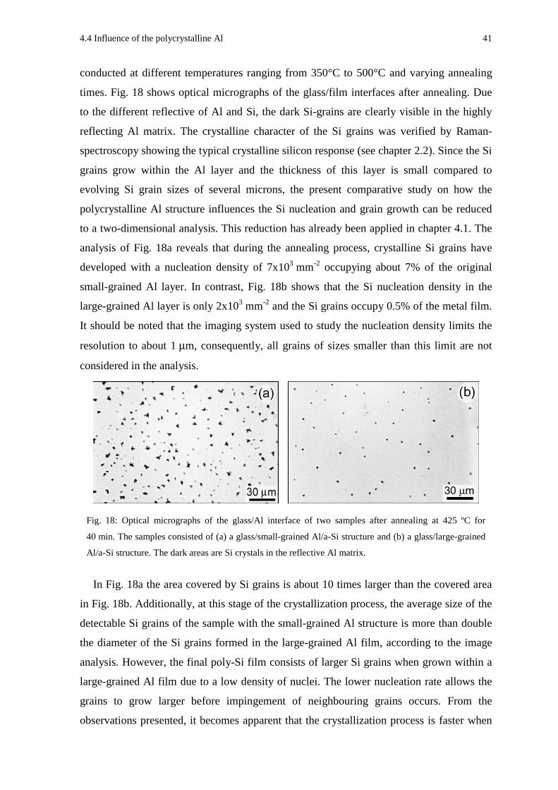
4.4 Influence of the polycrystalline Al 41
conducted at different temperatures ranging from 350°C to 500°C and varying annealing
times. Fig. 18 shows optical micrographs of the glass/film interfaces after annealing. Due
to the different reflective of Al and Si, the dark Si-grains are clearly visible in the highly
reflecting Al matrix. The crystalline character of the Si grains was verified by Raman-
spectroscopy showing the typical crystalline silicon response (see chapter 2.2). Since the Si
grains grow within the Al layer and the thickness of this layer is small compared to
evolving Si grain sizes of several microns, the present comparative study on how the
polycrystalline Al structure influences the Si nucleation and grain growth can be reduced
to a two-dimensional analysis. This reduction has already been applied in chapter 4.1. The
analysis of Fig. 18a reveals that during the annealing process, crystalline Si grains have
developed with a nucleation density of 7x103 mm-2 occupying about 7% of the original
small-grained Al layer. In contrast, Fig. 18b shows that the Si nucleation density in the
large-grained Al layer is only 2x103 mm-2 and the Si grains occupy 0.5% of the metal film.
It should be noted that the imaging system used to study the nucleation density limits the
resolution to about 1 µm, consequently, all grains of sizes smaller than this limit are not
considered in the analysis.
In Fig. 18a the area covered by Si grains is about 10 times larger than the covered area
in Fig. 18b. Additionally, at this stage of the crystallization process, the average size of the
detectable Si grains of the sample with the small-grained Al structure is more than double
the diameter of the Si grains formed in the large-grained Al film, according to the image
analysis. However, the final poly-Si film consists of larger Si grains when grown within a
large-grained Al film due to a low density of nuclei. The lower nucleation rate allows the
grains to grow larger before impingement of neighbouring grains occurs. From the
observations presented, it becomes apparent that the crystallization process is faster when
Fig. 18: Optical micrographs of the glass/Al interface of two samples after annealing at 425 ºC for
40 min. The samples consisted of (a) a glass/small-grained Al/a-Si structure and (b) a glass/large-grained
Al/a-Si structure. The dark areas are Si crystals in the reflective Al matrix.
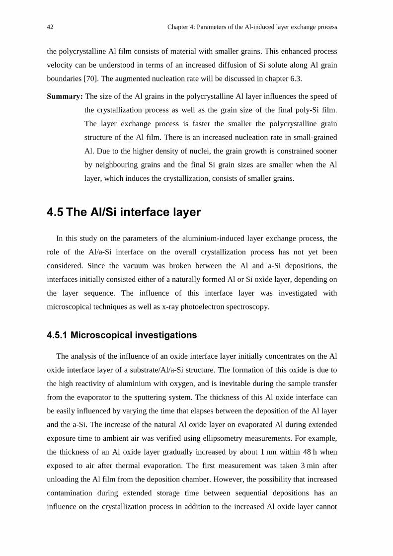
42 Chapter 4: Parameters of the Al-induced layer exchange process
the polycrystalline Al film consists of material with smaller grains. This enhanced process
velocity can be understood in terms of an increased diffusion of Si solute along Al grain
boundaries [70]. The augmented nucleation rate will be discussed in chapter 6.3.
' The size of the Al grains in the polycrystalline Al layer influences the speed of
the crystallization process as well as the grain size of the final poly-Si film.
The layer exchange process is faster the smaller the polycrystalline grain
structure of the Al film. There is an increased nucleation rate in small-grained
Al. Due to the higher density of nuclei, the grain growth is constrained sooner
by neighbouring grains and the final Si grain sizes are smaller when the Al
layer, which induces the crystallization, consists of smaller grains.
),%-
In this study on the parameters of the aluminium-induced layer exchange process, the
role of the Al/a-Si interface on the overall crystallization process has not yet been
considered. Since the vacuum was broken between the Al and a-Si depositions, the
interfaces initially consisted either of a naturally formed Al or Si oxide layer, depending on
the layer sequence. The influence of this interface layer was investigated with
microscopical techniques as well as x-ray photoelectron spectroscopy.
), .
The analysis of the influence of an oxide interface layer initially concentrates on the Al
oxide interface layer of a substrate/Al/a-Si structure. The formation of this oxide is due to
the high reactivity of aluminium with oxygen, and is inevitable during the sample transfer
from the evaporator to the sputtering system. The thickness of this Al oxide interface can
be easily influenced by varying the time that elapses between the deposition of the Al layer
and the a-Si. The increase of the natural Al oxide layer on evaporated Al during extended
exposure time to ambient air was verified using ellipsometry measurements. For example,
the thickness of an Al oxide layer gradually increased by about 1 nm within 48 h when
exposed to air after thermal evaporation. The first measurement was taken 3 min after
unloading the Al film from the deposition chamber. However, the possibility that increased
contamination during extended storage time between sequential depositions has an
influence on the crystallization process in addition to the increased Al oxide layer cannot
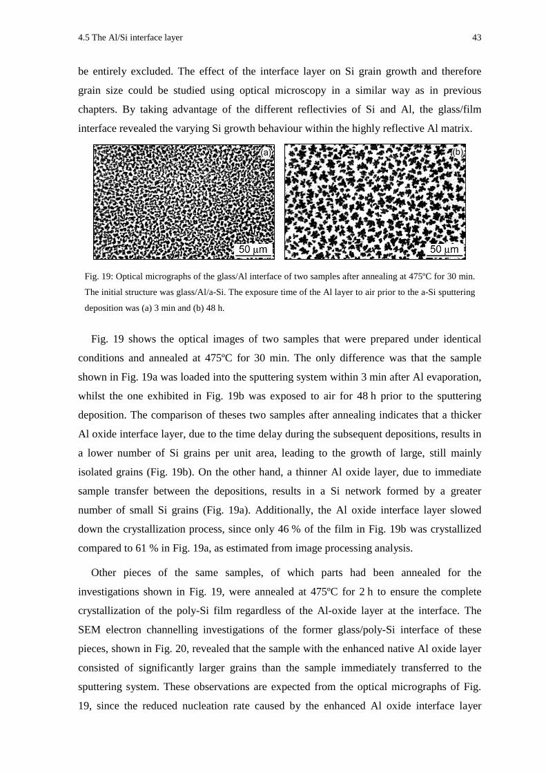
4.5 The Al/Si interface layer 43
be entirely excluded. The effect of the interface layer on Si grain growth and therefore
grain size could be studied using optical microscopy in a similar way as in previous
chapters. By taking advantage of the different reflectivies of Si and Al, the glass/film
interface revealed the varying Si growth behaviour within the highly reflective Al matrix.
Fig. 19 shows the optical images of two samples that were prepared under identical
conditions and annealed at 475ºC for 30 min. The only difference was that the sample
shown in Fig. 19a was loaded into the sputtering system within 3 min after Al evaporation,
whilst the one exhibited in Fig. 19b was exposed to air for 48 h prior to the sputtering
deposition. The comparison of theses two samples after annealing indicates that a thicker
Al oxide interface layer, due to the time delay during the subsequent depositions, results in
a lower number of Si grains per unit area, leading to the growth of large, still mainly
isolated grains (Fig. 19b). On the other hand, a thinner Al oxide layer, due to immediate
sample transfer between the depositions, results in a Si network formed by a greater
number of small Si grains (Fig. 19a). Additionally, the Al oxide interface layer slowed
down the crystallization process, since only 46 % of the film in Fig. 19b was crystallized
compared to 61 % in Fig. 19a, as estimated from image processing analysis.
Other pieces of the same samples, of which parts had been annealed for the
investigations shown in Fig. 19, were annealed at 475ºC for 2 h to ensure the complete
crystallization of the poly-Si film regardless of the Al-oxide layer at the interface. The
SEM electron channelling investigations of the former glass/poly-Si interface of these
pieces, shown in Fig. 20, revealed that the sample with the enhanced native Al oxide layer
consisted of significantly larger grains than the sample immediately transferred to the
sputtering system. These observations are expected from the optical micrographs of Fig.
19, since the reduced nucleation rate caused by the enhanced Al oxide interface layer
Fig. 19: Optical micrographs of the glass/Al interface of two samples after annealing at 475ºC for 30 min.
The initial structure was glass/Al/a-Si. The exposure time of the Al layer to air prior to the a-Si sputtering
deposition was (a) 3 min and (b) 48 h.
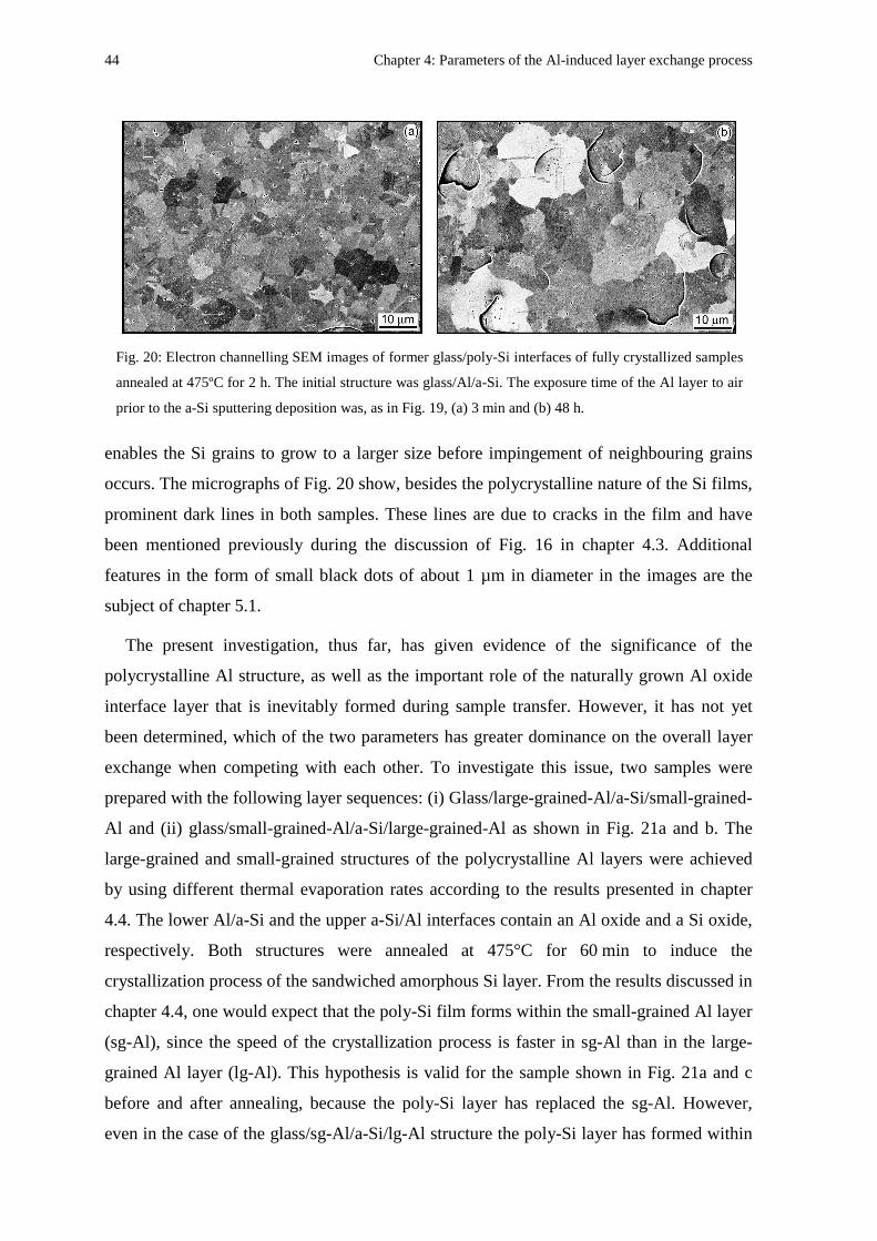
44 Chapter 4: Parameters of the Al-induced layer exchange process
enables the Si grains to grow to a larger size before impingement of neighbouring grains
occurs. The micrographs of Fig. 20 show, besides the polycrystalline nature of the Si films,
prominent dark lines in both samples. These lines are due to cracks in the film and have
been mentioned previously during the discussion of Fig. 16 in chapter 4.3. Additional
features in the form of small black dots of about 1 µm in diameter in the images are the
subject of chapter 5.1.
The present investigation, thus far, has given evidence of the significance of the
polycrystalline Al structure, as well as the important role of the naturally grown Al oxide
interface layer that is inevitably formed during sample transfer. However, it has not yet
been determined, which of the two parameters has greater dominance on the overall layer
exchange when competing with each other. To investigate this issue, two samples were
prepared with the following layer sequences: (i) Glass/large-grained-Al/a-Si/small-grained-
Al and (ii) glass/small-grained-Al/a-Si/large-grained-Al as shown in Fig. 21a and b. The
large-grained and small-grained structures of the polycrystalline Al layers were achieved
by using different thermal evaporation rates according to the results presented in chapter
4.4. The lower Al/a-Si and the upper a-Si/Al interfaces contain an Al oxide and a Si oxide,
respectively. Both structures were annealed at 475°C for 60 min to induce the
crystallization process of the sandwiched amorphous Si layer. From the results discussed in
chapter 4.4, one would expect that the poly-Si film forms within the small-grained Al layer
(sg-Al), since the speed of the crystallization process is faster in sg-Al than in the large-
grained Al layer (lg-Al). This hypothesis is valid for the sample shown in Fig. 21a and c
before and after annealing, because the poly-Si layer has replaced the sg-Al. However,
even in the case of the glass/sg-Al/a-Si/lg-Al structure the poly-Si layer has formed within
Fig. 20: Electron channelling SEM images of former glass/poly-Si interfaces of fully crystallized samples
annealed at 475ºC for 2 h. The initial structure was glass/Al/a-Si. The exposure time of the Al layer to air
prior to the a-Si sputtering deposition was, as in Fig. 19, (a) 3 min and (b) 48 h.
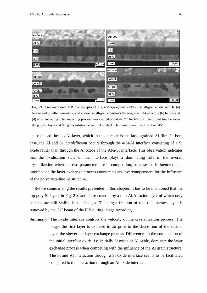
4.5 The Al/Si interface layer 45
and replaced the top Al layer, which in this sample is the large-grained Al film. In both
case, the Al and Si interdiffusion occurs through the a-Si/Al interface consisting of a Si
oxide rather than through the Al oxide of the Al/a-Si interface. This observation indicates
that the oxidisation state of the interface plays a dominating role in the overall
crystallization when the two parameters are in competition, because the influence of the
interface on the layer exchange process counteracts and overcompensates for the influence
of the polycrystalline Al structure.
Before summarising the results presented in this chapter, it has to be mentioned that the
top poly-Si layers in Fig. 21c and d are covered by a thin Al/Al oxide layer of which only
patches are still visible in the images. The larger fraction of this thin surface layer is
removed by the Ga+ beam of the FIB during image recording.
' The oxide interface controls the velocity of the crystallization process. The
longer the first layer is exposed to air prior to the deposition of the second
layer, the slower the layer exchange process. Differences in the composition of
the initial interface oxide, i.e. initially Si oxide or Al oxide, dominate the layer
exchange process when competing with the influence of the Al grain structure.
The Si and Al interaction through a Si oxide interface seems to be facilitated
compared to the interaction through an Al oxide interface.
Fig. 21: Cross-sectional FIB micrographs of a glass/large-grained-Al/a-Si/small-grained-Al sample (a)
before and (c) after annealing, and a glass/small-grained-Al/a-Si/large-grained-Al structure (b) before and
(d) after annealing. The annealing process was carried out at 475°C for 60 min. The bright line between
the poly-Si layer and the glass substrate is an FIB artefact. The samples are tilted by about 45º.
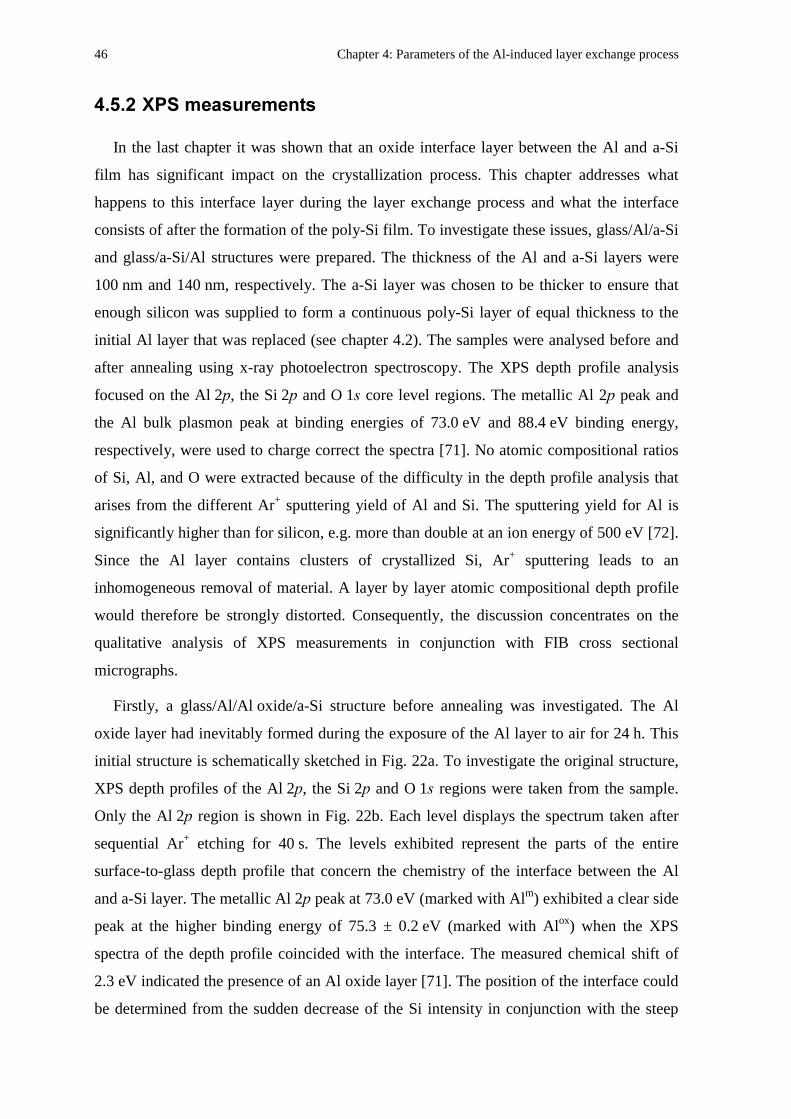
46 Chapter 4: Parameters of the Al-induced layer exchange process
),/(
In the last chapter it was shown that an oxide interface layer between the Al and a-Si
film has significant impact on the crystallization process. This chapter addresses what
happens to this interface layer during the layer exchange process and what the interface
consists of after the formation of the poly-Si film. To investigate these issues, glass/Al/a-Si
and glass/a-Si/Al structures were prepared. The thickness of the Al and a-Si layers were
100 nm and 140 nm, respectively. The a-Si layer was chosen to be thicker to ensure that
enough silicon was supplied to form a continuous poly-Si layer of equal thickness to the
initial Al layer that was replaced (see chapter 4.2). The samples were analysed before and
after annealing using x-ray photoelectron spectroscopy. The XPS depth profile analysis
focused on the Al 2, the Si 2 and O 1core level regions. The metallic Al 2 peak and
the Al bulk plasmon peak at binding energies of 73.0 eV and 88.4 eV binding energy,
respectively, were used to charge correct the spectra [71]. No atomic compositional ratios
of Si, Al, and O were extracted because of the difficulty in the depth profile analysis that
arises from the different Ar+ sputtering yield of Al and Si. The sputtering yield for Al is
significantly higher than for silicon, e.g. more than double at an ion energy of 500 eV [72].
Since the Al layer contains clusters of crystallized Si, Ar+ sputtering leads to an
inhomogeneous removal of material. A layer by layer atomic compositional depth profile
would therefore be strongly distorted. Consequently, the discussion concentrates on the
qualitative analysis of XPS measurements in conjunction with FIB cross sectional
micrographs.
Firstly, a glass/Al/Al oxide/a-Si structure before annealing was investigated. The Al
oxide layer had inevitably formed during the exposure of the Al layer to air for 24 h. This
initial structure is schematically sketched in Fig. 22a. To investigate the original structure,
XPS depth profiles of the Al 2, the Si 2 and O 1regions were taken from the sample.
Only the Al 2 region is shown in Fig. 22b. Each level displays the spectrum taken after
sequential Ar+ etching for 40 s. The levels exhibited represent the parts of the entire
surface-to-glass depth profile that concern the chemistry of the interface between the Al
and a-Si layer. The metallic Al 2 peak at 73.0 eV (marked with Alm) exhibited a clear side
peak at the higher binding energy of 75.3 ± 0.2 eV (marked with Alox) when the XPS
spectra of the depth profile coincided with the interface. The measured chemical shift of
2.3 eV indicated the presence of an Al oxide layer [71]. The position of the interface could
be determined from the sudden decrease of the Si intensity in conjunction with the steep
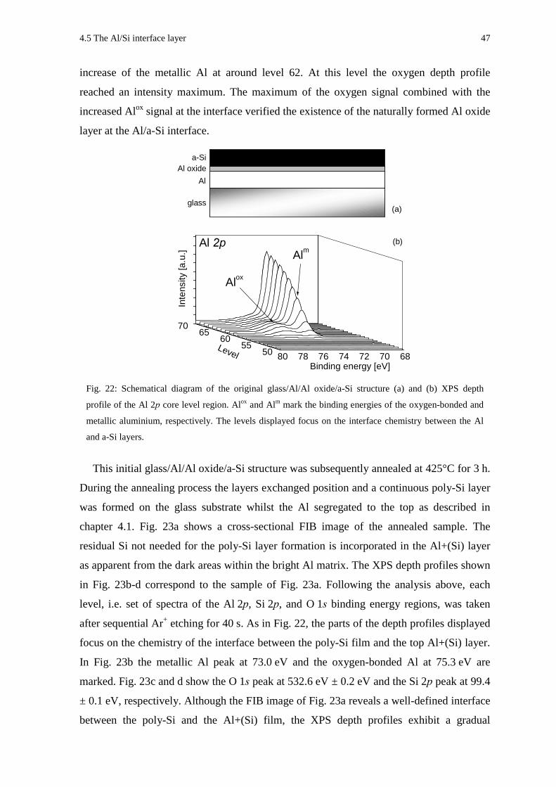
4.5 The Al/Si interface layer 47
increase of the metallic Al at around level 62. At this level the oxygen depth profile
reached an intensity maximum. The maximum of the oxygen signal combined with the
increased Alox signal at the interface verified the existence of the naturally formed Al oxide
layer at the Al/a-Si interface.
This initial glass/Al/Al oxide/a-Si structure was subsequently annealed at 425°C for 3 h.
During the annealing process the layers exchanged position and a continuous poly-Si layer
was formed on the glass substrate whilst the Al segregated to the top as described in
chapter 4.1. Fig. 23a shows a cross-sectional FIB image of the annealed sample. The
residual Si not needed for the poly-Si layer formation is incorporated in the Al+(Si) layer
as apparent from the dark areas within the bright Al matrix. The XPS depth profiles shown
in Fig. 23b-d correspond to the sample of Fig. 23a. Following the analysis above, each
level, i.e. set of spectra of the Al 2, Si 2, and O 1 binding energy regions, was taken
after sequential Ar+ etching for 40 s. As in Fig. 22, the parts of the depth profiles displayed
focus on the chemistry of the interface between the poly-Si film and the top Al+(Si) layer.
In Fig. 23b the metallic Al peak at 73.0 eV and the oxygen-bonded Al at 75.3 eV are
marked. Fig. 23c and d show the O 1 peak at 532.6 eV ± 0.2 eV and the Si 2 peak at 99.4
± 0.1 eV, respectively. Although the FIB image of Fig. 23a reveals a well-defined interface
between the poly-Si and the Al+(Si) film, the XPS depth profiles exhibit a gradual
80 78 76 74 72 70 68
7065
6055
50
Alm
Alox
Al
Inte
nsity
[a.u
.]
Binding energy [eV]
Level
glass
a-Si
Al
Al oxide
(a)
(b)
Fig. 22: Schematical diagram of the original glass/Al/Al oxide/a-Si structure (a) and (b) XPS depth
profile of the Al 2 core level region. Alox and Alm mark the binding energies of the oxygen-bonded and
metallic aluminium, respectively. The levels displayed focus on the interface chemistry between the Al
and a-Si layers.
48 Chapter 4: Parameters of the Al-induced layer exchange process
transition. This underlines the distortion effect inherent to the depth profile investigations
due to the strong difference in sputtering yield of the materials as mentioned above.
Nevertheless, the comparative analysis of the three depth profiles reveals that the
intensities of the Alox and the O 1 peak have a local maximum at level 44, whilst the Si 2
peak has a local minimum at almost the same level (level 43). The coincidence of the three
80 78 76 74 72 70 68
55 50 45 40 35 30
Level 44
AlmAlox
(b)Al 2
Inte
nsity
[a.u
.]
Binding energy [eV]
Level
538 536 534 532 530 528 526
55 50 45 40 35 30
Level 44
(c)O 1
Inte
nsity
[a.u
.]
Binding energy (eV)
Level
106 104 102 100 98 96
55 50 45 40 35 30
Level 44
(d)Si 2
Inte
nsity
[a.u
.]
Binding energy [eV]
Level
Fig. 23: Analysis of an initial glass/Al/a-Si structure after annealing and the layer exchange process: (a)
Cross-sectional FIB micrograph and (b-d) depth profiles of the XPS spectra.
4.5 The Al/Si interface layer 49
extrema is a strong indication of the existence of an Al oxide interface layer between the
poly-Si and Al+(Si) layer after crystallization. Additionally, the top Al layer was etched off
the sample. The bar poly-Si film was again investigated using XPS. On the surface of the
Si film, Al oxide was again detected by analysing the binding energy shift of oxygen-
bonded aluminium. This means that the Al oxide remains on the surface of the poly-Si film
even after Al etching.
To complement the measurements on samples before and after full crystallisation, XPS
depth profile investigations were conducted on a glass/Al/a-Si sample that was only
partially crystallized (75 % according to optical micrograph analysis). The results
concerning the chemistry of the interface layer also revealed the existence of an Al oxide
interface layer. Consequently, the XPS measurements give evidence that an Al oxide layer
exists at the interface of the original, the partially annealed and the fully annealed layer
structure. This means that the naturally formed Al oxide film between the initially
deposited Al and a-Si layer sequence remains stable throughout the entire crystallization
process. A stable interface oxide seems surprising considering that during the formation of
the continuous poly-Si layer the Al and Si films exchange positions completely – not a
single atom of either layer remains where it was. The Al oxide interface layer is most
likely not an entirely stoichiometric Al2O3 layer, because the Al 2 binding energy shift is
2.3 eV compared to 2.7 eV in bulk Al2O3. This value resembles the data reported by
Flodstrom et al. on their in-situ XPS observations of the initial growth of thin non-
stoichiometric Al oxide layers on polycrystalline Al [71].
For the structure so far investigated using XPS, the Al was deposited prior to the a-Si,
but in the previous chapter it was shown that a layer exchange also occurs when the a-Si is
buried under an Al film. Initially the a-Si/Al interface of a glass/a-Si/Al structure consists
of an naturally formed SiO2, because the silicon is exposed to air prior to the Al deposition.
The role of the interface oxide in this structure is also analysed using XPS. Fig. 24a shows
the FIB cross-sectional micrograph of such an inverse layer sequence, compared to the one
investigated previously, after annealing. During the 3 hour annealing process at 425°C a
continuous poly-Si layer had formed replacing the top Al layer. The Al was repelled from
the growing crystalline Si phase and segregated to the glass substrate. There, it formed an
Al+(Si) layer with the residual Si that was not incorporated in the continuous poly-Si layer.
The XPS depth profile analysis of this sample is shown in Fig. 24b-d. As discussed for Fig.
23 the levels presented do not constitute the entire surface-to-glass profile but concentrate
on the chemistry of the Al/Si interface. From Fig. 24c it is apparent that the O 1 peak
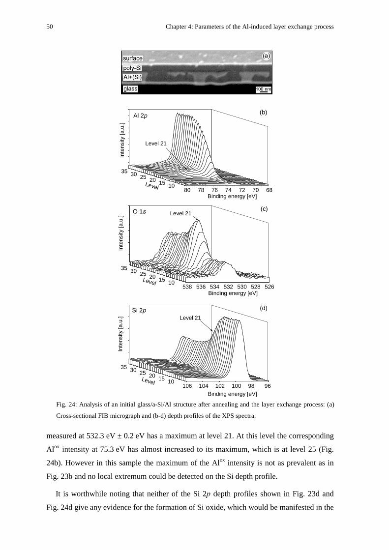
50 Chapter 4: Parameters of the Al-induced layer exchange process
measured at 532.3 eV ± 0.2 eV has a maximum at level 21. At this level the corresponding
Alox intensity at 75.3 eV has almost increased to its maximum, which is at level 25 (Fig.
24b). However in this sample the maximum of the Alox intensity is not as prevalent as in
Fig. 23b and no local extremum could be detected on the Si depth profile.
It is worthwhile noting that neither of the Si 2 depth profiles shown in Fig. 23d and
Fig. 24d give any evidence for the formation of Si oxide, which would be manifested in the
80 78 76 74 72 70 68
35 30 25 20 15 10
Level 21
(b)Al 2In
tens
ity [a
.u.]
Binding energy [eV]
Level
538 536 534 532 530 528 526
35 30 25 20 15 10
Level 21(c)O 1
Inte
nsity
[a.u
.]
Binding energy [eV]
Level
106 104 102 100 98 96
35 30 25 20 15 10
Level 21
(d)Si 2
Inte
nsity
[a.u
.]
Binding energy [eV]
Level
Fig. 24: Analysis of an initial glass/a-Si/Al structure after annealing and the layer exchange process: (a)
Cross-sectional FIB micrograph and (b-d) depth profiles of the XPS spectra.
4.5 The Al/Si interface layer 51
form of a chemical shift of the Si 2 core level to a binding energy in the region of 103 eV
± 2 eV [73]. Oxidised silicon was not found to reduce significantly under Ar+ ion
bombardment. The increased oxygen content at the interface as apparent from Fig. 24c can
therefore be attributed to an Al oxide layer. Thus, the glass/Al+(Si)/poly-Si structure of
Fig. 24a also contains an Al oxide interface film between the two layers, very similar to the
inverse structure analysed in Fig. 23.
The comparison of the O 1 depth profiles shown in Fig. 23c and Fig. 24c indicates that
in both cases the oxygen content is higher in the Al+(Si) film than in the pure poly-Si film.
This is in contrast to the initial structures where a higher concentration of oxygen in the
sputtered a-Si than in the evaporated Al layer was detected. In chapter 4.1 it was shown
that the poly-Si grows within the Al whilst the Al is repelled from the growing crystalline
Si phase and segregates into the initial a-Si film. The lower oxygen content in the poly-Si
layer than in the Al+(Si) after crystallization can therefore be attributed to the gettering
properties of Al when the a-Si film dissociates into the metal [74]. The ability of Al to bind
oxygen can be seen as an additional advantage in the formation of continuous high-quality
poly-Si using aluminium-induced crystallization. However, detailed investigations of the
variations in oxygen concentration in the films using, for example, secondary ion mass
spectroscopy have not been conducted in the work presented.
' The oxide interface between the adjacent Al and Si layer seems to remain at
the interface throughout the entire layer exchange process, although most of the
Si and Al atoms change position from one side of the interface to the other. The
interface consists of an overall stable Al oxide. However, this oxide layer
should not be considered as a homogenous film but rather a film with local
variations in the structure so that an exchange process can occur in the first
place (see chapter 6.1).
),&0
In the previous two chapters, the existence of a stable interface oxide between the Al
and Si layer was shown. This interface oxide layer remains at its original position
throughout the entire layer exchange. Is this oxidised interface mandatory for the exchange
process? This question can be answered by studying the interaction of adjacent a-Si and Al
films when deposited in the one vacuum system.
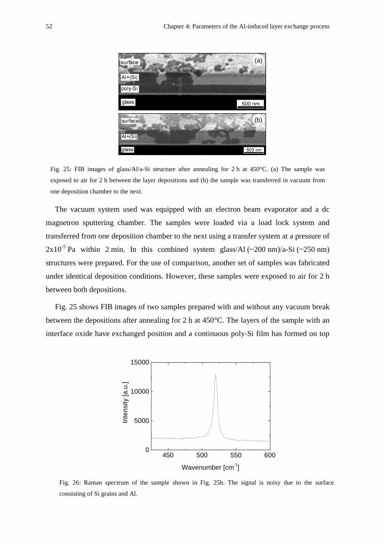
52 Chapter 4: Parameters of the Al-induced layer exchange process
The vacuum system used was equipped with an electron beam evaporator and a dc
magnetron sputtering chamber. The samples were loaded via a load lock system and
transferred from one deposition chamber to the next using a transfer system at a pressure of
2x10⁻⁵ Pa within 2 min. In this combined system glass/Al (~200 nm)/a-Si (~250 nm)
structures were prepared. For the use of comparison, another set of samples was fabricated
under identical deposition conditions. However, these samples were exposed to air for 2 h
between both depositions.
Fig. 25 shows FIB images of two samples prepared with and without any vacuum break
between the depositions after annealing for 2 h at 450°C. The layers of the sample with an
interface oxide have exchanged position and a continuous poly-Si film has formed on top
(a)
(b)
Fig. 25: FIB images of glass/Al/a-Si structure after annealing for 2 h at 450°C. (a) The sample was
exposed to air for 2 h between the layer depositions and (b) the sample was transferred in vacuum from
one deposition chamber to the next.
450 500 550 6000
5000
10000
15000
Inte
nsity
[a.u
.]
Wavenumber [cm-1]
Fig. 26: Raman spectrum of the sample shown in Fig. 25b. The signal is noisy due to the surface
consisting of Si grains and Al.
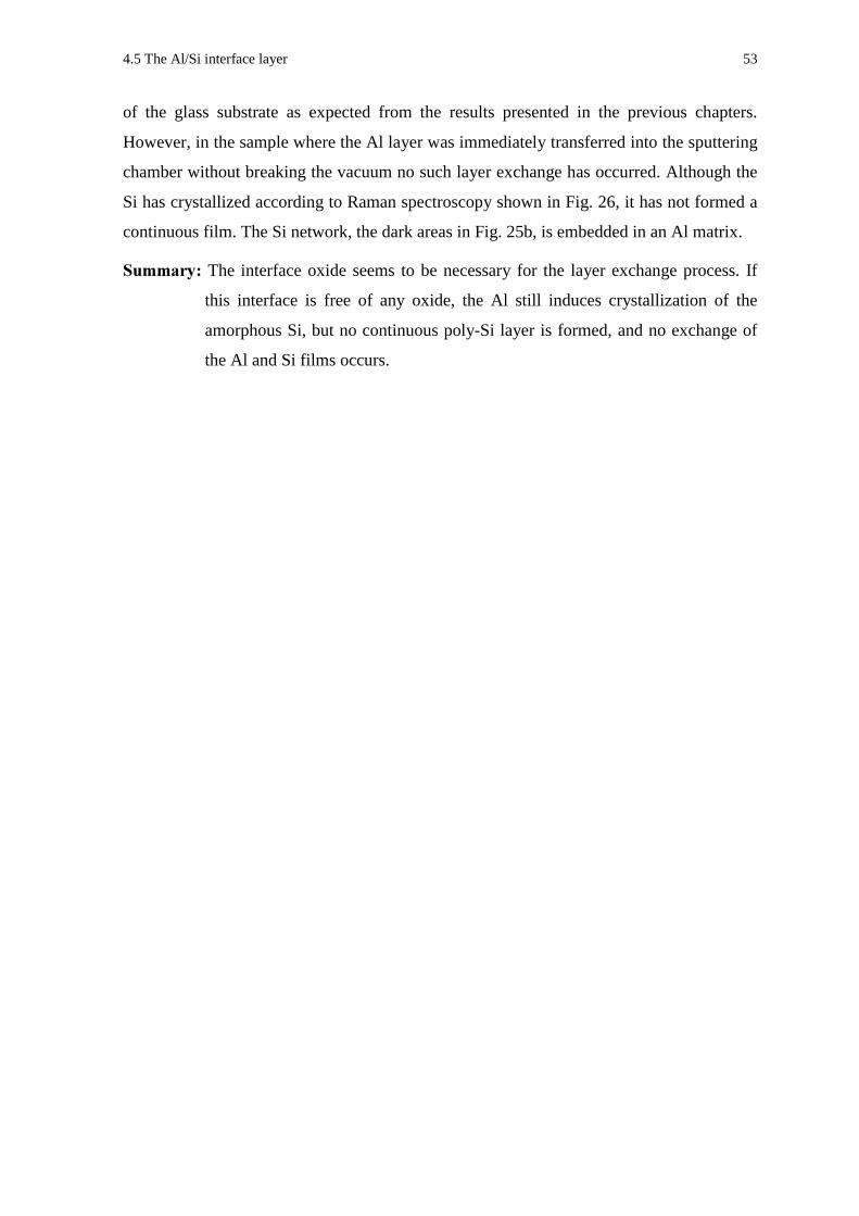
4.5 The Al/Si interface layer 53
of the glass substrate as expected from the results presented in the previous chapters.
However, in the sample where the Al layer was immediately transferred into the sputtering
chamber without breaking the vacuum no such layer exchange has occurred. Although the
Si has crystallized according to Raman spectroscopy shown in Fig. 26, it has not formed a
continuous film. The Si network, the dark areas in Fig. 25b, is embedded in an Al matrix.
' The interface oxide seems to be necessary for the layer exchange process. If
this interface is free of any oxide, the Al still induces crystallization of the
amorphous Si, but no continuous poly-Si layer is formed, and no exchange of
the Al and Si films occurs.

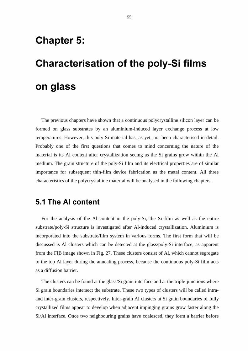
55
,
The previous chapters have shown that a continuous polycrystalline silicon layer can be
formed on glass substrates by an aluminium-induced layer exchange process at low
temperatures. However, this poly-Si material has, as yet, not been characterised in detail.
Probably one of the first questions that comes to mind concerning the nature of the
material is its Al content after crystallization seeing as the Si grains grow within the Al
medium. The grain structure of the poly-Si film and its electrical properties are of similar
importance for subsequent thin-film device fabrication as the metal content. All three
characteristics of the polycrystalline material will be analysed in the following chapters.
,%
For the analysis of the Al content in the poly-Si, the Si film as well as the entire
substrate/poly-Si structure is investigated after Al-induced crystallization. Aluminium is
incorporated into the substrate/film system in various forms. The first form that will be
discussed is Al clusters which can be detected at the glass/poly-Si interface, as apparent
from the FIB image shown in Fig. 27. These clusters consist of Al, which cannot segregate
to the top Al layer during the annealing process, because the continuous poly-Si film acts
as a diffusion barrier.
The clusters can be found at the glass/Si grain interface and at the triple-junctions where
Si grain boundaries intersect the substrate. These two types of clusters will be called intra-
and inter-grain clusters, respectively. Inter-grain Al clusters at Si grain boundaries of fully
crystallized films appear to develop when adjacent impinging grains grow faster along the
Si/Al interface. Once two neighbouring grains have coalesced, they form a barrier before
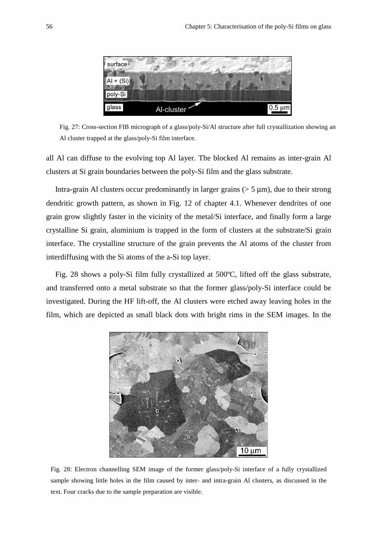
56 Chapter 5: Characterisation of the poly-Si films on glass
all Al can diffuse to the evolving top Al layer. The blocked Al remains as inter-grain Al
clusters at Si grain boundaries between the poly-Si film and the glass substrate.
Intra-grain Al clusters occur predominantly in larger grains (> 5 µm), due to their strong
dendritic growth pattern, as shown in Fig. 12 of chapter 4.1. Whenever dendrites of one
grain grow slightly faster in the vicinity of the metal/Si interface, and finally form a large
crystalline Si grain, aluminium is trapped in the form of clusters at the substrate/Si grain
interface. The crystalline structure of the grain prevents the Al atoms of the cluster from
interdiffusing with the Si atoms of the a-Si top layer.
Fig. 28 shows a poly-Si film fully crystallized at 500ºC, lifted off the glass substrate,
and transferred onto a metal substrate so that the former glass/poly-Si interface could be
investigated. During the HF lift-off, the Al clusters were etched away leaving holes in the
film, which are depicted as small black dots with bright rims in the SEM images. In the
Fig. 27: Cross-section FIB micrograph of a glass/poly-Si/Al structure after full crystallization showing an
Al cluster trapped at the glass/poly-Si film interface.
Fig. 28: Electron channelling SEM image of the former glass/poly-Si interface of a fully crystallized
sample showing little holes in the film caused by inter- and intra-grain Al clusters, as discussed in the
text. Four cracks due to the sample preparation are visible.
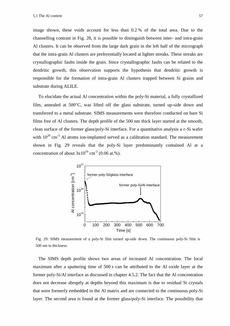
5.1 The Al content 57
image shown, these voids account for less than 0.2 % of the total area. Due to the
channelling contrast in Fig. 28, it is possible to distinguish between inter- and intra-grain
Al clusters. It can be observed from the large dark grain in the left half of the micrograph
that the intra-grain Al clusters are preferentially located at lighter streaks. These streaks are
crystallographic faults inside the grain. Since crystallographic faults can be related to the
dendritic growth, this observation supports the hypothesis that dendritic growth is
responsible for the formation of intra-grain Al clusters trapped between Si grains and
substrate during ALILE.
To elucidate the actual Al concentration within the poly-Si material, a fully crystallized
film, annealed at 500°C, was lifted off the glass substrate, turned up-side down and
transferred to a metal substrate. SIMS measurements were therefore conducted on bare Si
films free of Al clusters. The depth profile of the 500 nm thick layer started at the smooth,
clean surface of the former glass/poly-Si interface. For a quantitative analysis a c-Si wafer
with 1020 cm-3 Al atoms ion-implanted served as a calibration standard. The measurement
shown in Fig. 29 reveals that the poly-Si layer predominantly contained Al at a
concentration of about 3x1019 cm-3 (0.06 at.%).
The SIMS depth profile shows two areas of increased Al concentration. The local
maximum after a sputtering time of 500 s can be attributed to the Al oxide layer at the
former poly-Si/Al interface as discussed in chapter 4.5.2. The fact that the Al concentration
does not decrease abruptly at depths beyond this maximum is due to residual Si crystals
that were formerly embedded in the Al matrix and are connected to the continuous poly-Si
layer. The second area is found at the former glass/poly-Si interface. The possibility that
0 100 200 300 400 500 600 700
1019
1020
1021
former poly-Si/Al interface
former poly-Si/glass interface
Al c
once
ntra
tion
[cm
-3]
Time [s]
Fig. 29: SIMS measurement of a poly-Si film turned up-side down. The continuous poly-Si film is
500 nm in thickness.
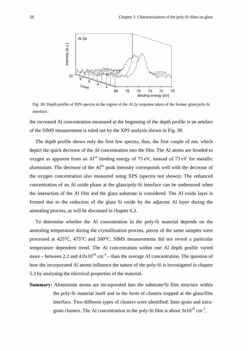
58 Chapter 5: Characterisation of the poly-Si films on glass
the increased Al concentration measured at the beginning of the depth profile is an artefact
of the SIMS measurement is ruled out by the XPS analysis shown in Fig. 30.
The depth profile shows only the first few spectra, thus, the first couple of nm, which
depict the quick decrease of the Al concentration into the film. The Al atoms are bonded to
oxygen as apparent from an Alox binding energy of 75 eV, instead of 73 eV for metallic
aluminium. The decrease of the Alox peak intensity corresponds well with the decrease of
the oxygen concentration also measured using XPS (spectra not shown). The enhanced
concentration of an Al oxide phase at the glass/poly-Si interface can be understood when
the interaction of the Al film and the glass substrate is considered. The Al oxide layer is
formed due to the reduction of the glass Si oxide by the adjacent Al layer during the
annealing process, as will be discussed in chapter 6.2.
To determine whether the Al concentration in the poly-Si material depends on the
annealing temperature during the crystallization process, pieces of the same samples were
processed at 425°C, 475°C and 500°C. SIMS measurements did not reveal a particular
temperature dependent trend. The Al concentration within one Al depth profile varied
more – between 2.2 and 4.0x1019 cm-3 – than the average Al concentration. The question of
how the incorporated Al atoms influence the nature of the poly-Si is investigated in chapter
5.3 by analysing the electrical properties of the material.
' Aluminium atoms are incorporated into the substrate/Si film structure within
the poly-Si material itself and in the form of clusters trapped at the glass/film
interface. Two different types of clusters were identified: Inter-grain and intra-
grain clusters. The Al concentration in the poly-Si film is about 3x1019 cm-3.
108
64
280 78 76 74 72 70
Al 2
Inte
nsity
[a.u
.]
Binding energy [eV]
Level
Fig. 30: Depth profile of XPS spectra in the region of the Al 2 response taken of the former glass/poly-Si
interface.
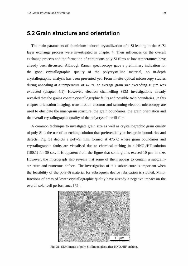
5.2 Grain structure and orientation 59
,1
The main parameters of aluminium-induced crystallization of a-Si leading to the Al/Si
layer exchange process were investigated in chapter 4. Their influences on the overall
exchange process and the formation of continuous poly-Si films at low temperatures have
already been discussed. Although Raman spectroscopy gave a preliminary indication for
the good crystallographic quality of the polycrystalline material, no in-depth
crystallographic analysis has been presented yet. From in-situ optical microscopy studies
during annealing at a temperature of 475°C an average grain size exceeding 10 µm was
extracted (chapter 4.1). However, electron channelling SEM investigations already
revealed that the grains contain crystallographic faults and possible twin boundaries. In this
chapter orientation imaging, transmission electron and scanning electron microscopy are
used to elucidate the inner-grain structure, the grain boundaries, the grain orientation and
the overall crystallographic quality of the polycrystalline Si film.
A common technique to investigate grain size as well as crystallographic grain quality
of poly-Si is the use of an etching solution that preferentially etches grain boundaries and
defects. Fig. 31 depicts a poly-Si film formed at 475°C where grain boundaries and
crystallographic faults are visualised due to chemical etching in a HNO3/HF solution
(100:1) for 30 sec. It is apparent from the figure that some grains exceed 10 µm in size.
However, the micrograph also reveals that some of them appear to contain a subgrain-
structure and numerous defects. The investigation of this substructure is important when
the feasibility of the poly-Si material for subsequent device fabrication is studied. Minor
fractions of areas of lower crystallographic quality have already a negative impact on the
overall solar cell performance [75].
Fig. 31: SEM image of poly-Si film on glass after HNO3/HF etching.
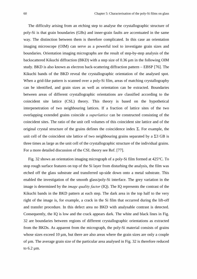
60 Chapter 5: Characterisation of the poly-Si films on glass
The difficulty arising from an etching step to analyse the crystallographic structure of
poly-Si is that grain boundaries (GBs) and inner-grain faults are accentuated in the same
way. The distinction between them is therefore complicated. In this case an orientation
imaging microscope (OIM) can serve as a powerful tool to investigate grain sizes and
boundaries. Orientation imaging micrographs are the result of step-by-step analysis of the
backscattered Kikuchi diffraction (BKD) with a step size of 0.36 µm in the following OIM
study. BKD is also known as electron back-scattering diffraction pattern – EBSP [76]. The
Kikuchi bands of the BKD reveal the crystallographic orientation of the analysed spot.
When a grid-like pattern is scanned over a poly-Si film, areas of matching crystallography
can be identified, and grain sizes as well as orientation can be extracted. Boundaries
between areas of different crystallographic orientations are classified according to the
coincident site lattice (CSL) theory. This theory is based on the hypothetical
interpenetration of two neighbouring lattices. If a fraction of lattice sites of the two
overlapping extended grains coincide a can be constructed consisting of the
coincident sites. The ratio of the unit cell volumes of this coincident site lattice and of the
original crystal structure of the grains defines the coincidence index Σ. For example, the
unit cell of the coincident site lattice of two neighbouring grains separated by a Σ3 GB is
three times as large as the unit cell of the crystallographic structure of the individual grains.
For a more detailed discussion of the CSL theory see Ref. [77].
Fig. 32 shows an orientation imaging micrograph of a poly-Si film formed at 425°C. To
stop rough surface features on top of the Si layer from disturbing the analysis, the film was
etched off the glass substrate and transferred up-side down onto a metal substrate. This
enabled the investigation of the smooth glass/poly-Si interface. The grey variation in the
image is determined by the (IQ). The IQ represents the contrast of the
Kikuchi bands in the BKD pattern at each step. The dark area in the top half to the very
right of the image is, for example, a crack in the Si film that occurred during the lift-off
and transfer procedure. In this defect area no BKD with analysable contrast is detected.
Consequently, the IQ is low and the crack appears dark. The white and black lines in Fig.
32 are boundaries between regions of different crystallographic orientations as extracted
from the BKDs. As apparent from the micrograph, the poly-Si material consists of grains
whose sizes exceed 10 µm, but there are also areas where the grain sizes are only a couple
of µm. The average grain size of the particular area analysed in Fig. 32 is therefore reduced
to 6.2 µm.
5.2 Grain structure and orientation 61
The existence of small grains seems to be in contradiction to the results presented in
chapter 4.1. According to the in-situ optical microscopy investigations, the formation of
new nuclei is suppressed at an early stage of the crystallization process. This suppression
of further nucleation enables the growth of large grains. It will be discussed later that the
suppression of nucleus formation is due to the interference of already existing and growing
grains at an early stage of ALILE (see chapter 6.4). Therefore, if large grains are formed,
only very few small grains should be present. In this case and s means above
10 µm and below 5 µm in diameter, respectively. The apparent contradiction between the
OIM results and the optical microscopy investigations will be analysed in the following
paragraphs.
The grain boundaries of the poly-Si material analysed in Fig. 32 can be distinguished
into two groups: (a) Coincident site lattice grain boundaries, CSL GBs, with coincidence
index Σ3 and Σ9 (white lines) and (b) all other types of GBs (black lines). The ratio of Σ3
to Σ9 GBs amongst the white lines is about unity. It is apparent from the micrograph that
the grains in the small-grained areas are predominantly separated by Σ3 and Σ9 grain
boundaries. Both types of CSL GBs have low atomic distortions [78]. The low distortion is
evident from Fig. 33, which shows a schematical presentation of a grain boundary with a
coincidence index Σ3. This type of twin boundary can be theoretically constructed by
dividing a Si crystal along the 111 plane, rotating one half by 180° around the <111>
Fig. 32: Orientation imaging micrograph of the former glass/poly-Si interface of a sample annealed at
450°C. Grain sizes and grain boundaries are depicted; the white lines are Σ3 and Σ9 boundaries, the
black lines represent all the other grain boundaries.
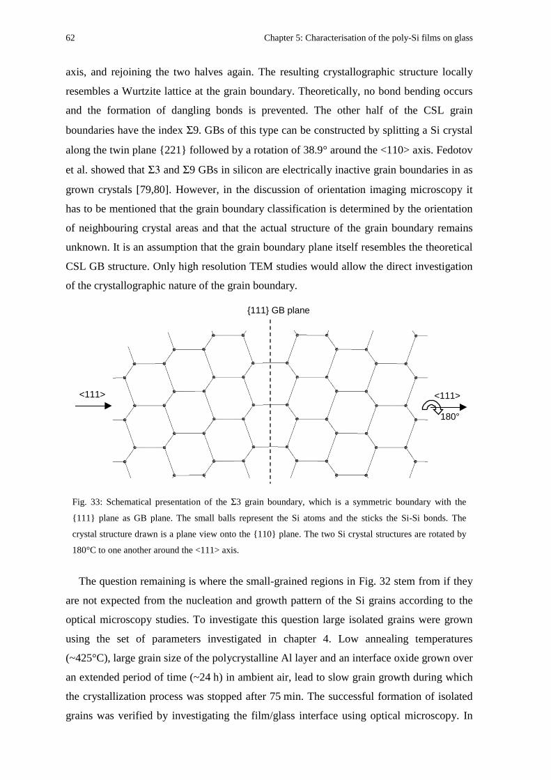
62 Chapter 5: Characterisation of the poly-Si films on glass
axis, and rejoining the two halves again. The resulting crystallographic structure locally
resembles a Wurtzite lattice at the grain boundary. Theoretically, no bond bending occurs
and the formation of dangling bonds is prevented. The other half of the CSL grain
boundaries have the index Σ9. GBs of this type can be constructed by splitting a Si crystal
along the twin plane 221 followed by a rotation of 38.9° around the <110> axis. Fedotov
et al. showed that Σ3 and Σ9 GBs in silicon are electrically inactive grain boundaries in as
grown crystals [79,80]. However, in the discussion of orientation imaging microscopy it
has to be mentioned that the grain boundary classification is determined by the orientation
of neighbouring crystal areas and that the actual structure of the grain boundary remains
unknown. It is an assumption that the grain boundary plane itself resembles the theoretical
CSL GB structure. Only high resolution TEM studies would allow the direct investigation
of the crystallographic nature of the grain boundary.
The question remaining is where the small-grained regions in Fig. 32 stem from if they
are not expected from the nucleation and growth pattern of the Si grains according to the
optical microscopy studies. To investigate this question large isolated grains were grown
using the set of parameters investigated in chapter 4. Low annealing temperatures
(~425°C), large grain size of the polycrystalline Al layer and an interface oxide grown over
an extended period of time (~24 h) in ambient air, lead to slow grain growth during which
the crystallization process was stopped after 75 min. The successful formation of isolated
grains was verified by investigating the film/glass interface using optical microscopy. In
111 GB plane
<111> <111>
180°
Fig. 33: Schematical presentation of the Σ3 grain boundary, which is a symmetric boundary with the
111 plane as GB plane. The small balls represent the Si atoms and the sticks the Si-Si bonds. The
crystal structure drawn is a plane view onto the 110 plane. The two Si crystal structures are rotated by
180°C to one another around the <111> axis.
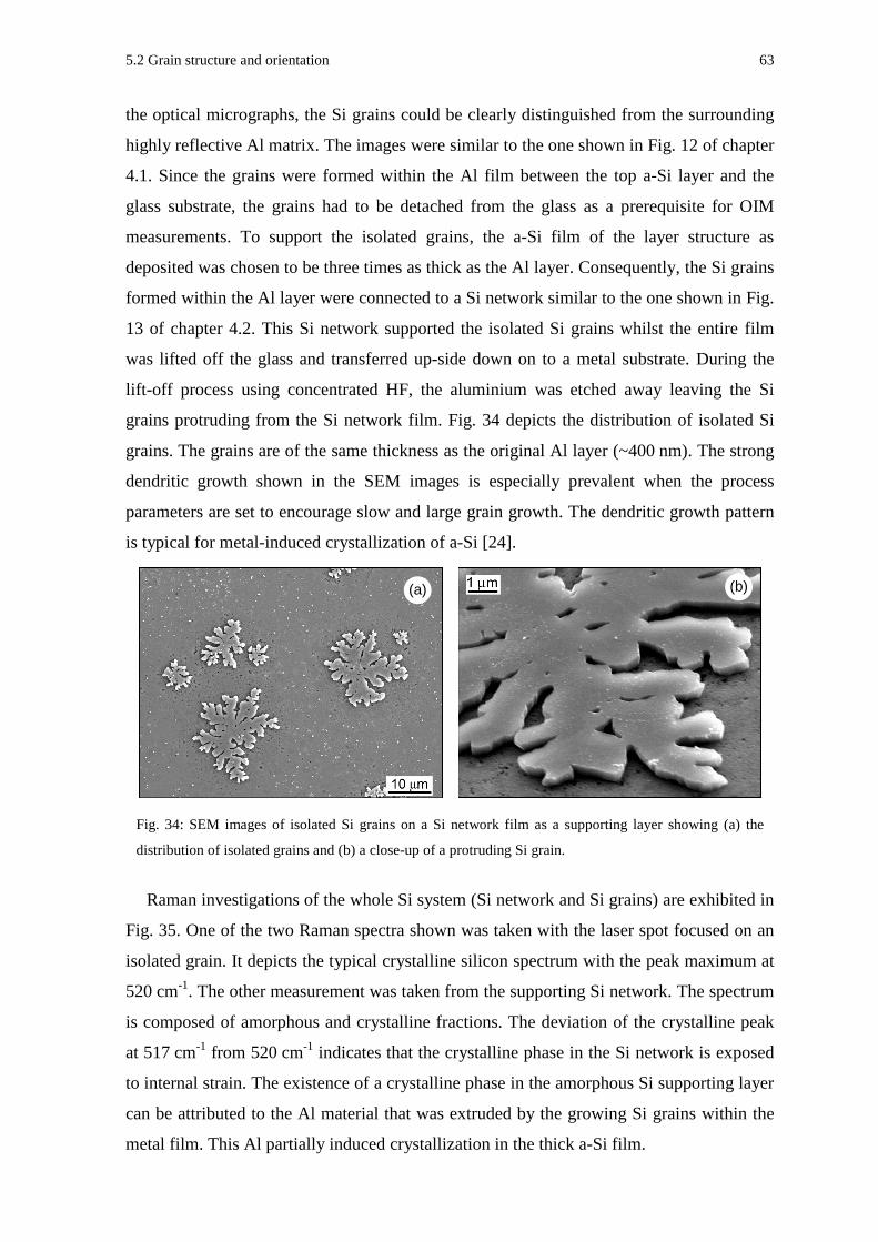
5.2 Grain structure and orientation 63
the optical micrographs, the Si grains could be clearly distinguished from the surrounding
highly reflective Al matrix. The images were similar to the one shown in Fig. 12 of chapter
4.1. Since the grains were formed within the Al film between the top a-Si layer and the
glass substrate, the grains had to be detached from the glass as a prerequisite for OIM
measurements. To support the isolated grains, the a-Si film of the layer structure as
deposited was chosen to be three times as thick as the Al layer. Consequently, the Si grains
formed within the Al layer were connected to a Si network similar to the one shown in Fig.
13 of chapter 4.2. This Si network supported the isolated Si grains whilst the entire film
was lifted off the glass and transferred up-side down on to a metal substrate. During the
lift-off process using concentrated HF, the aluminium was etched away leaving the Si
grains protruding from the Si network film. Fig. 34 depicts the distribution of isolated Si
grains. The grains are of the same thickness as the original Al layer (~400 nm). The strong
dendritic growth shown in the SEM images is especially prevalent when the process
parameters are set to encourage slow and large grain growth. The dendritic growth pattern
is typical for metal-induced crystallization of a-Si [24].
Raman investigations of the whole Si system (Si network and Si grains) are exhibited in
Fig. 35. One of the two Raman spectra shown was taken with the laser spot focused on an
isolated grain. It depicts the typical crystalline silicon spectrum with the peak maximum at
520 cm-1. The other measurement was taken from the supporting Si network. The spectrum
is composed of amorphous and crystalline fractions. The deviation of the crystalline peak
at 517 cm-1 from 520 cm-1 indicates that the crystalline phase in the Si network is exposed
to internal strain. The existence of a crystalline phase in the amorphous Si supporting layer
can be attributed to the Al material that was extruded by the growing Si grains within the
metal film. This Al partially induced crystallization in the thick a-Si film.
(a) (b)
Fig. 34: SEM images of isolated Si grains on a Si network film as a supporting layer showing (a) the
distribution of isolated grains and (b) a close-up of a protruding Si grain.
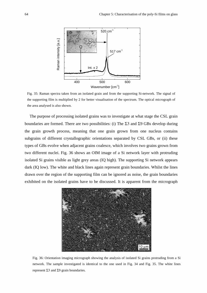
64 Chapter 5: Characterisation of the poly-Si films on glass
The purpose of processing isolated grains was to investigate at what stage the CSL grain
boundaries are formed. There are two possibilities: (i) The Σ3 and Σ9 GBs develop during
the grain growth process, meaning that one grain grown from one nucleus contains
subgrains of different crystallographic orientations separated by CSL GBs, or (ii) these
types of GBs evolve when adjacent grains coalesce, which involves two grains grown from
two different nuclei. Fig. 36 shows an OIM image of a Si network layer with protruding
isolated Si grains visible as light grey areas (IQ high). The supporting Si network appears
dark (IQ low). The white and black lines again represent grain boundaries. Whilst the lines
drawn over the region of the supporting film can be ignored as noise, the grain boundaries
exhibited on the isolated grains have to be discussed. It is apparent from the micrograph
400 500 600
Int. x 2
517 cm-1
520 cm-1
Ram
an in
tens
ity [a
.u.]
Wavenumber [cm-1]
Fig. 35: Raman spectra taken from an isolated grain and from the supporting Si-network. The signal of
the supporting film is multiplied by 2 for better visualisation of the spectrum. The optical micrograph of
the area analysed is also shown.
Fig. 36: Orientation imaging micrograph showing the analysis of isolated Si grains protruding from a Si
network. The sample investigated is identical to the one used in Fig. 34 and Fig. 35. The white lines
represent Σ3 and Σ9 grain boundaries.
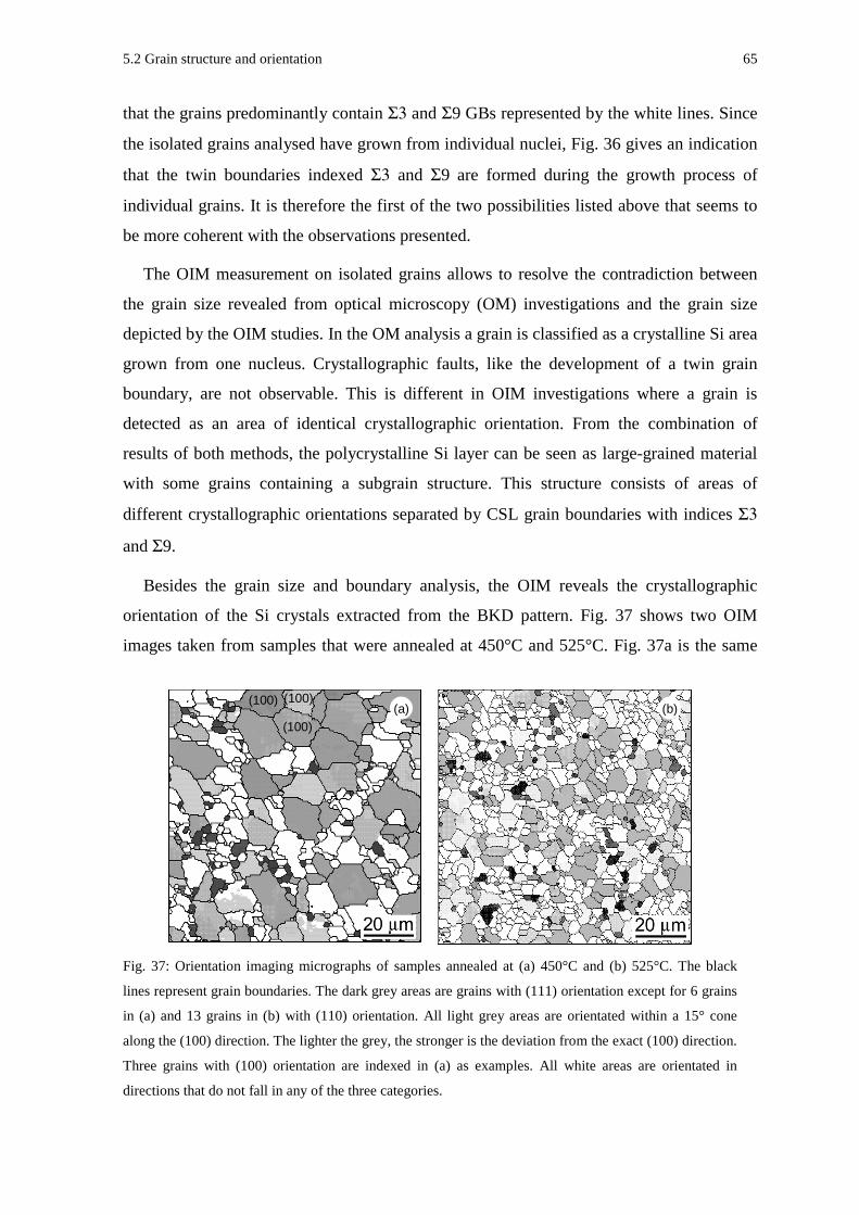
5.2 Grain structure and orientation 65
that the grains predominantly contain Σ3 and Σ9 GBs represented by the white lines. Since
the isolated grains analysed have grown from individual nuclei, Fig. 36 gives an indication
that the twin boundaries indexed Σ3 and Σ9 are formed during the growth process of
individual grains. It is therefore the first of the two possibilities listed above that seems to
be more coherent with the observations presented.
The OIM measurement on isolated grains allows to resolve the contradiction between
the grain size revealed from optical microscopy (OM) investigations and the grain size
depicted by the OIM studies. In the OM analysis a grain is classified as a crystalline Si area
grown from one nucleus. Crystallographic faults, like the development of a twin grain
boundary, are not observable. This is different in OIM investigations where a grain is
detected as an area of identical crystallographic orientation. From the combination of
results of both methods, the polycrystalline Si layer can be seen as large-grained material
with some grains containing a subgrain structure. This structure consists of areas of
different crystallographic orientations separated by CSL grain boundaries with indices Σ3
and Σ9.
Besides the grain size and boundary analysis, the OIM reveals the crystallographic
orientation of the Si crystals extracted from the BKD pattern. Fig. 37 shows two OIM
images taken from samples that were annealed at 450°C and 525°C. Fig. 37a is the same
(a) (b)(100)
(100)(100)
Fig. 37: Orientation imaging micrographs of samples annealed at (a) 450°C and (b) 525°C. The black
lines represent grain boundaries. The dark grey areas are grains with (111) orientation except for 6 grains
in (a) and 13 grains in (b) with (110) orientation. All light grey areas are orientated within a 15° cone
along the (100) direction. The lighter the grey, the stronger is the deviation from the exact (100) direction.
Three grains with (100) orientation are indexed in (a) as examples. All white areas are orientated in
directions that do not fall in any of the three categories.
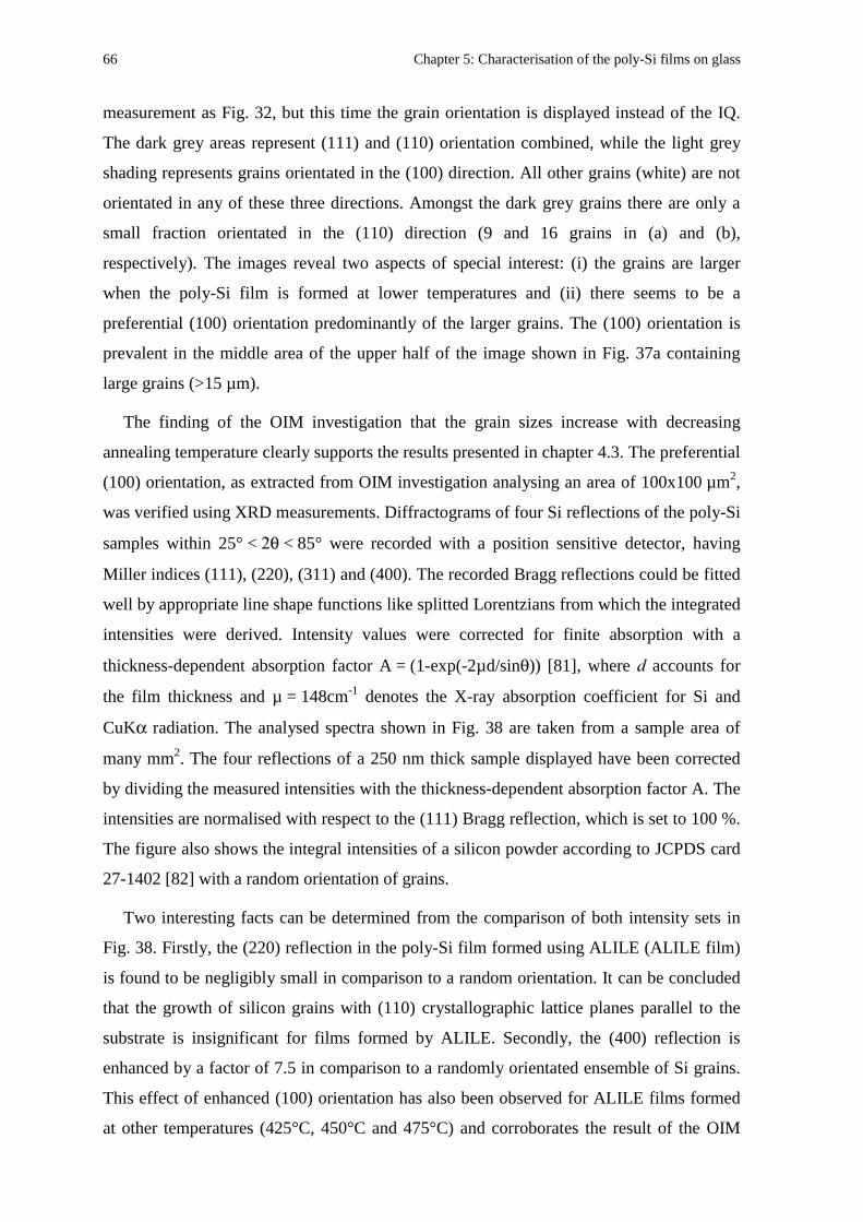
66 Chapter 5: Characterisation of the poly-Si films on glass
measurement as Fig. 32, but this time the grain orientation is displayed instead of the IQ.
The dark grey areas represent (111) and (110) orientation combined, while the light grey
shading represents grains orientated in the (100) direction. All other grains (white) are not
orientated in any of these three directions. Amongst the dark grey grains there are only a
small fraction orientated in the (110) direction (9 and 16 grains in (a) and (b),
respectively). The images reveal two aspects of special interest: (i) the grains are larger
when the poly-Si film is formed at lower temperatures and (ii) there seems to be a
preferential (100) orientation predominantly of the larger grains. The (100) orientation is
prevalent in the middle area of the upper half of the image shown in Fig. 37a containing
large grains (>15 µm).
The finding of the OIM investigation that the grain sizes increase with decreasing
annealing temperature clearly supports the results presented in chapter 4.3. The preferential
(100) orientation, as extracted from OIM investigation analysing an area of 100x100 µm2,
was verified using XRD measurements. Diffractograms of four Si reflections of the poly-Si
samples within 25° < 2θ < 85° were recorded with a position sensitive detector, having
Miller indices (111), (220), (311) and (400). The recorded Bragg reflections could be fitted
well by appropriate line shape functions like splitted Lorentzians from which the integrated
intensities were derived. Intensity values were corrected for finite absorption with a
thickness-dependent absorption factor A = (1-exp(-2µd/sinθ)) [81], where accounts for
the film thickness and µ = 148cm-1 denotes the X-ray absorption coefficient for Si and
CuKα radiation. The analysed spectra shown in Fig. 38 are taken from a sample area of
many mm2. The four reflections of a 250 nm thick sample displayed have been corrected
by dividing the measured intensities with the thickness-dependent absorption factor A. The
intensities are normalised with respect to the (111) Bragg reflection, which is set to 100 %.
The figure also shows the integral intensities of a silicon powder according to JCPDS card
27-1402 [82] with a random orientation of grains.
Two interesting facts can be determined from the comparison of both intensity sets in
Fig. 38. Firstly, the (220) reflection in the poly-Si film formed using ALILE (ALILE film)
is found to be negligibly small in comparison to a random orientation. It can be concluded
that the growth of silicon grains with (110) crystallographic lattice planes parallel to the
substrate is insignificant for films formed by ALILE. Secondly, the (400) reflection is
enhanced by a factor of 7.5 in comparison to a randomly orientated ensemble of Si grains.
This effect of enhanced (100) orientation has also been observed for ALILE films formed
at other temperatures (425°C, 450°C and 475°C) and corroborates the result of the OIM
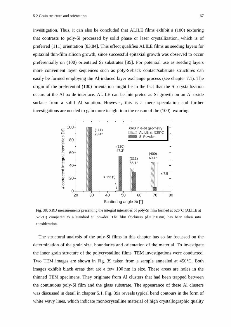
5.2 Grain structure and orientation 67
investigation. Thus, it can also be concluded that ALILE films exhibit a (100) texturing
that contrasts to poly-Si processed by solid phase or laser crystallization, which is of
preferred (111) orientation [83,84]. This effect qualifies ALILE films as seeding layers for
epitaxial thin-film silicon growth, since successful epitaxial growth was observed to occur
preferentially on (100) orientated Si substrates [85]. For potential use as seeding layers
more convenient layer sequences such as poly-Si/back contact/substrate structures can
easily be formed employing the Al-induced layer exchange process (see chapter 7.1). The
origin of the preferential (100) orientation might lie in the fact that the Si crystallization
occurs at the Al oxide interface. ALILE can be interpreted as Si growth on an Al oxide
surface from a solid Al solution. However, this is a mere speculation and further
investigations are needed to gain more insight into the reason of the (100) texturing.
The structural analysis of the poly-Si films in this chapter has so far focussed on the
determination of the grain size, boundaries and orientation of the material. To investigate
the inner grain structure of the polycrystalline films, TEM investigations were conducted.
Two TEM images are shown in Fig. 39 taken from a sample annealed at 450°C. Both
images exhibit black areas that are a few 100 nm in size. These areas are holes in the
thinned TEM specimens. They originate from Al clusters that had been trapped between
the continuous poly-Si film and the glass substrate. The appearance of these Al clusters
was discussed in detail in chapter 5.1. Fig. 39a reveals typical bend contours in the form of
white wavy lines, which indicate monocrystalline material of high crystallographic quality
20 30 40 50 60 70 800
20
40
60
80
100
x 7.5
< 1% (!)
(111)28.4°
(220)47.3°
(311)56.1°
(400)69.1°
-co
rrec
ted
inte
gral
inte
nsiti
es [%
]
Scattering angle 2θ [°]
XRD in θ−2θ geometry ALILE at 525°C Si Powder
Fig. 38: XRD measurements presenting the integral intensities of poly-Si film formed at 525°C (ALILE at
525°C) compared to a standard Si powder. The film thickness (d = 250 nm) has been taken into
consideration.
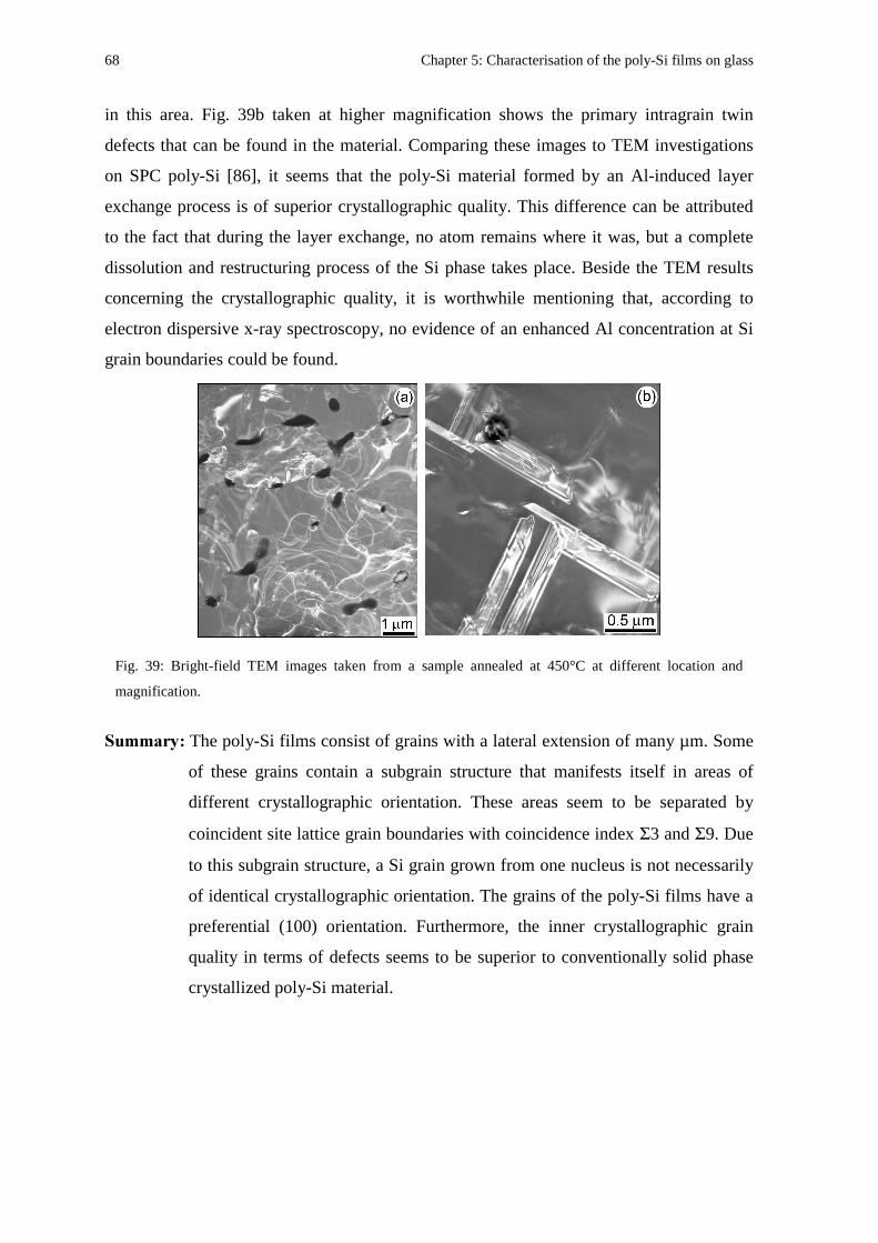
68 Chapter 5: Characterisation of the poly-Si films on glass
in this area. Fig. 39b taken at higher magnification shows the primary intragrain twin
defects that can be found in the material. Comparing these images to TEM investigations
on SPC poly-Si [86], it seems that the poly-Si material formed by an Al-induced layer
exchange process is of superior crystallographic quality. This difference can be attributed
to the fact that during the layer exchange, no atom remains where it was, but a complete
dissolution and restructuring process of the Si phase takes place. Beside the TEM results
concerning the crystallographic quality, it is worthwhile mentioning that, according to
electron dispersive x-ray spectroscopy, no evidence of an enhanced Al concentration at Si
grain boundaries could be found.
' The poly-Si films consist of grains with a lateral extension of many µm. Some
of these grains contain a subgrain structure that manifests itself in areas of
different crystallographic orientation. These areas seem to be separated by
coincident site lattice grain boundaries with coincidence index Σ3 and Σ9. Due
to this subgrain structure, a Si grain grown from one nucleus is not necessarily
of identical crystallographic orientation. The grains of the poly-Si films have a
preferential (100) orientation. Furthermore, the inner crystallographic grain
quality in terms of defects seems to be superior to conventionally solid phase
crystallized poly-Si material.
Fig. 39: Bright-field TEM images taken from a sample annealed at 450°C at different location and
magnification.
5.3 Electrical properties 69
,&'
Chapter 5.1 revealed that the poly-Si material formed by an aluminium-induced layer
exchange process contains 3x1019 cm-3 Al atoms after full crystallization. The incorporated
Al atoms influence the electrical properties of the polycrystalline Si film. The investigation
of the electrical characteristics of the material is a mandatory task, if any subsequent
device fabrication, e.g. solar cells, is considered. The resistivity, the free carrier
concentration and their mobility are important properties, which are the subject of this
chapter. The measurements were conducted on poly-Si films on glass where the Al that
had segregated to the top of the film during the crystallization process was etched off to
expose the bare polycrystalline material. The following chapter is divided into three
sections. The first section comprises the investigation of the basic electrical nature of
ALILE poly-Si by exemplary measurements of a Si film annealed at 500°C. The second
section analyses how some of the electrical properties vary depending on the temperature
of the ALILE process. The third section discusses the ratio of electrically active to non-
active Al atoms incorporated in the polycrystalline silicon. The results are only
summarised at the very end of this chapter.
,&2
In order to determine the basic electrical properties of a poly-Si layer formed at 500°C,
Hall effect measurements were performed between 13 and 470 K. At room temperature the
measured values of resistivity ρ, hole concentration p, and Hall mobility µH were
0.041 Ωcm, 2.6x1018 cm-3, and 56.3 cm2/Vs, respectively. However, by investigating four
sample pieces from the same specimen, slight variations could be detected. The lowest
result of the Hall mobility (54.0 cm2/Vs) was correlated to the highest hole concentration
(2.86x1018 cm-3). Therefore higher carrier concentrations are connected to lower mobilities
indicating that impurity scattering is the dominant scattering process [87] rather than
variations of the crystal quality or of the influence of grain boundaries. The high carrier
concentration is due to the incorporation of Al atoms on substitutional lattice sites of poly-
Si. The substitutional point defect AlSi is a well known shallow acceptor in Si, having an
activation energy of 68 meV [88]. The values of the Hall mobility µH,p are in the vicinity of
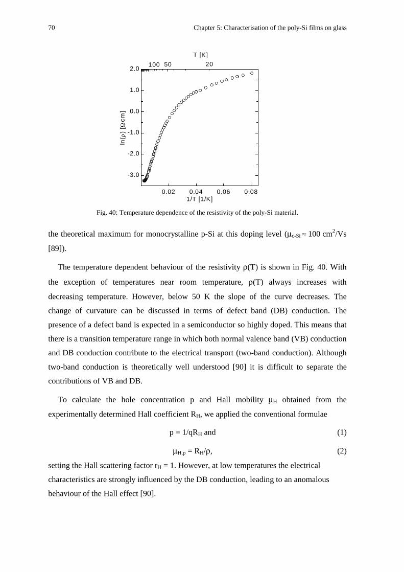
70 Chapter 5: Characterisation of the poly-Si films on glass
the theoretical maximum for monocrystalline p-Si at this doping level (µc-Si ≈ 100 cm2/Vs
[89]).
The temperature dependent behaviour of the resistivity ρ(T) is shown in Fig. 40. With
the exception of temperatures near room temperature, ρ(T) always increases with
decreasing temperature. However, below 50 K the slope of the curve decreases. The
change of curvature can be discussed in terms of defect band (DB) conduction. The
presence of a defect band is expected in a semiconductor so highly doped. This means that
there is a transition temperature range in which both normal valence band (VB) conduction
and DB conduction contribute to the electrical transport (two-band conduction). Although
two-band conduction is theoretically well understood [90] it is difficult to separate the
contributions of VB and DB.
To calculate the hole concentration p and Hall mobility µH obtained from the
experimentally determined Hall coefficient RH, we applied the conventional formulae
p = 1/qRH and (1)
µH,p = RH/ρ, (2)
setting the Hall scattering factor rH = 1. However, at low temperatures the electrical
characteristics are strongly influenced by the DB conduction, leading to an anomalous
behaviour of the Hall effect [90].
0.02 0.04 0.06 0.08
-3.0
-2.0
-1.0
0.0
1.0
2.0100 50 20
T [K]
ln(ρ
) [Ω
cm]
1/T [1/K]
Fig. 40: Temperature dependence of the resistivity of the poly-Si material.
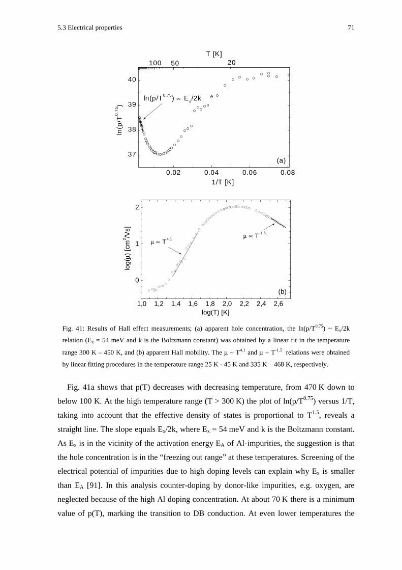
5.3 Electrical properties 71
Fig. 41a shows that p(T) decreases with decreasing temperature, from 470 K down to
below 100 K. At the high temperature range (T > 300 K) the plot of ln(p/T0.75) versus 1/T,
taking into account that the effective density of states is proportional to T1.5, reveals a
straight line. The slope equals Ex/2k, where Ex = 54 meV and k is the Boltzmann constant.
As Ex is in the vicinity of the activation energy EA of Al-impurities, the suggestion is that
the hole concentration is in the “freezing out range” at these temperatures. Screening of the
electrical potential of impurities due to high doping levels can explain why Ex is smaller
than EA [91]. In this analysis counter-doping by donor-like impurities, e.g. oxygen, are
neglected because of the high Al doping concentration. At about 70 K there is a minimum
value of p(T), marking the transition to DB conduction. At even lower temperatures the
0.02 0.04 0.06 0.08
37
38
39
40
ln(p/T0.75) ∝ Ex/2k
1/T [K]
ln(p
/T0
.75)
(a)
100 50 20 T [K]
1,0 1,2 1,4 1,6 1,8 2,0 2,2 2,4 2,6
0
1
2
µ ∝ T -1.5
(b)
µ ∝ T 4.1
log(
µ) [c
m2 /V
s]
log(T) [K]
Fig. 41: Results of Hall effect measurements; (a) apparent hole concentration, the ln(p/T0.75) ~ Ex/2k
relation (Ex = 54 meV and k is the Boltzmann constant) was obtained by a linear fit in the temperature
range 300 K – 450 K, and (b) apparent Hall mobility. The µ ∼ T4.1 and µ ∼ T-1.5 relations were obtained
by linear fitting procedures in the temperature range 25 K - 45 K and 335 K – 468 K, respectively.
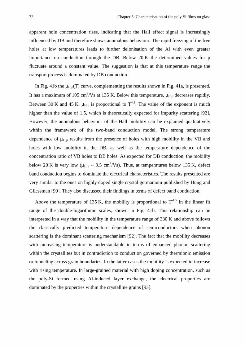
72 Chapter 5: Characterisation of the poly-Si films on glass
apparent hole concentration rises, indicating that the Hall effect signal is increasingly
influenced by DB and therefore shows anomalous behaviour. The rapid freezing of the free
holes at low temperatures leads to further deionisation of the Al with even greater
importance on conduction through the DB. Below 20 K the determined values for p
fluctuate around a constant value. The suggestion is that at this temperature range the
transport process is dominated by DB conduction.
In Fig. 41b the µH,p(T) curve, complementing the results shown in Fig. 41a, is presented.
It has a maximum of 105 cm2/Vs at 135 K. Below this temperature, µH,p decreases rapidly.
Between 30 K and 45 K, µH,p is proportional to T4.1. The value of the exponent is much
higher than the value of 1.5, which is theoretically expected for impurity scattering [92].
However, the anomalous behaviour of the Hall mobility can be explained qualitatively
within the framework of the two-band conduction model. The strong temperature
dependence of µH,p results from the presence of holes with high mobility in the VB and
holes with low mobility in the DB, as well as the temperature dependence of the
concentration ratio of VB holes to DB holes. As expected for DB conduction, the mobility
below 20 K is very low (µH,p ≈ 0.5 cm2/Vs). Thus, at temperatures below 135 K, defect
band conduction begins to dominate the electrical characteristics. The results presented are
very similar to the ones on highly doped single crystal germanium published by Hung and
Gliessman [90]. They also discussed their findings in terms of defect band conduction.
Above the temperature of 135 K, the mobility is proportional to T-1.5 in the linear fit
range of the double-logarithmic scales, shown in Fig. 41b. This relationship can be
interpreted in a way that the mobility in the temperature range of 330 K and above follows
the classically predicted temperature dependence of semiconductors when phonon
scattering is the dominant scattering mechanism [92]. The fact that the mobility decreases
with increasing temperature is understandable in terms of enhanced phonon scattering
within the crystallites but in contradiction to conduction governed by thermionic emission
or tunneling across grain boundaries. In the latter cases the mobility is expected to increase
with rising temperature. In large-grained material with high doping concentration, such as
the poly-Si formed using Al-induced layer exchange, the electrical properties are
dominated by the properties within the crystalline grains [93].
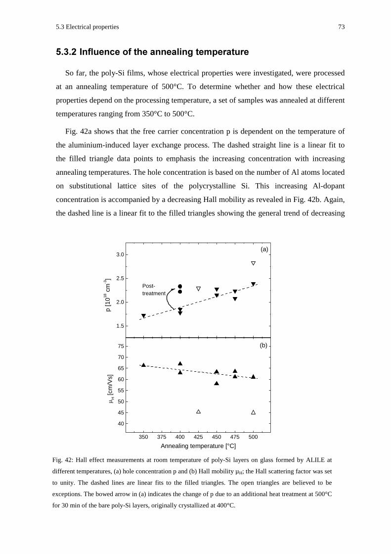
5.3 Electrical properties 73
,&
So far, the poly-Si films, whose electrical properties were investigated, were processed
at an annealing temperature of 500°C. To determine whether and how these electrical
properties depend on the processing temperature, a set of samples was annealed at different
temperatures ranging from 350°C to 500°C.
Fig. 42a shows that the free carrier concentration p is dependent on the temperature of
the aluminium-induced layer exchange process. The dashed straight line is a linear fit to
the filled triangle data points to emphasis the increasing concentration with increasing
annealing temperatures. The hole concentration is based on the number of Al atoms located
on substitutional lattice sites of the polycrystalline Si. This increasing Al-dopant
concentration is accompanied by a decreasing Hall mobility as revealed in Fig. 42b. Again,
the dashed line is a linear fit to the filled triangles showing the general trend of decreasing
1.5
2.0
2.5
3.0(a)
Post-treatment
p [1
018 c
m-3]
350 375 400 425 450 475 500
40
45
50
55
60
65
70
75 (b)
µ H [c
m/V
s]
Annealing temperature [°C]
Fig. 42: Hall effect measurements at room temperature of poly-Si layers on glass formed by ALILE at
different temperatures, (a) hole concentration p and (b) Hall mobility µH; the Hall scattering factor was set
to unity. The dashed lines are linear fits to the filled triangles. The open triangles are believed to be
exceptions. The bowed arrow in (a) indicates the change of p due to an additional heat treatment at 500°C
for 30 min of the bare poly-Si layers, originally crystallized at 400°C.
74 Chapter 5: Characterisation of the poly-Si films on glass
mobility. This means that at higher concentrations of substitutional Al atoms, impurity
scattering leads to a lower hole mobility in the poly-Si material. Nevertheless, Hall
mobilities were measured to be between 60 and 70 cm/Vs for all but two samples. It is
unclear why two samples, one annealed at 425°C and the other at 500°C (open triangles in
Fig. 42a and b), showed results, which did not follow the trends.
It is interesting to note that the lower carrier concentration of poly-Si films annealed at
lower temperatures could be increased by additional heat treatment of the bare films after
the metallic Al was etched off. This behaviour is indicated in Fig. 42a by the bowed arrow
for two samples originally annealed at 400°C. After Al etching, the samples were again
heated, though at a higher temperature of 500°C for 30 min. This post-treatment increased
the carrier concentration from approximately 1.8x1018 cm-3 to 2.3x1018 cm-3, a similar
value to the concentration of the samples which were annealed at 500°C during ALILE. To
understand this behaviour it is necessary to distinguish between three types of Al atoms: (i)
Electrically active Al on substitutional sites ( −subAl ), (ii) electrically non-active Al on
substitutional sites ( 0subAl ) and (iii) Al on non-substitutional sites, such as on interstitial
sites and at grain boundaries (Alx). In addition to these three types of incorporated Al, the
Al clusters trapped at the glass/poly-Si interface (see chapter 5.1) have to be taken into
account. The observation that the carrier concentration increases after the post-treatment
indicates that Alx atoms and/or Al atoms from Al clusters could be activated by additional
heat-treatment at 500°C to occupy lattice sites. The additional Al atoms on substitutional
sites contribute to the measured hole concentration. Remarks on the quantitative
relationship between 0subAl , −
subAl and Alx are given in the next section.
,&& 33%
Whilst the measured hole concentration is equal to the ionised Al atoms on
substitutional sites, −subAl , the SIMS results presented in chapter 5.1 give the total amount
of Al in the poly-Si material Altot. To compare the Hall-effect measurements with the
SIMS result it is necessary to calculate the total concentration of Al atoms on substitutional
sites, Alsub. To estimate the ratio of Al atoms on substitutional sites to the ones on non-
substitutional sites it is firstly necessary to extract the Fermi energy using the following
relationship [94]:
5.3 Electrical properties 75
[ ]∫∞−
−ρ=0
v dE)E(f1)E(p (3)
v(E) is the density of states in the valence band and f(E) the Fermi distribution. The
valence band edge is set equal to zero. Assuming a parabolic band structure of the valence
band, equation (3) transforms into
∫ ∞− − +−
π=
0
kT/)EE(
5.1
dv2
dE1e
Em2
2
1p
F(4)
with mdv being the valence-band density-of-states effective mass, EF the Fermi level, the
reduced Planck constant and k the Boltzmann constant. Since the free carrier concentration
revealed in section 5.3.1 is high, the following analysis refrains from approximating the
Fermi distribution by the Boltzmann distribution to avoid inconsistencies due to
degeneration effects of the highly doped poly-Si material. Defining the Fermi integral as
∫∞
η− +π=η
0 )x(2/1 dx1e
x2)(F (5)
and substituting
kT
Ex −= and
kT
E F−=η (6)
equation (4) can be written as
]kT/E[FNp F2/1V −⋅= (7)
with
5.1
2dv
V 2
kTm2N
π=
. (8)
Green gave for the effective density of states the value [95]
NV = 3.10x1019 cm-3 (9)
by using his reassessed value for the valence-band density-of-states effective mass at
T = 300 K. Measuring the free carrier concentration and using Fermi integral tables,
equation (7) allows to extract the Fermi energy [96]. In the specific case analysed, the
value of the free carrier concentration p is set to 2.5x1018 cm-3 according to the Hall effect
measurements of the poly-Si material formed at 500°C (see chapters 5.3.1 and 5.3.2), and
it follows that EF equals 65 ± 2 meV. The error stems from variations in the determined
hole concentration.
76 Chapter 5: Characterisation of the poly-Si films on glass
The free carrier concentration is equal to the negatively ionised Al atoms on
substitutional Si lattice site. For the time being, counter-doping due to impurity
incorporation such as oxygen is neglected. The ratio x of the substitutional, ionised Al
atoms −subAl to the total amount of substitutional Al atoms subAl is determined by the
following relationship [57]
1eg
1
Al
Alx
kT/)EE(sub
sub
FA +⋅== −
−
. (10)
EA is the activation energy and g is the ground-state degeneracy factor, which equals 4 for
acceptor levels in Si. Using the value determined in chapter 5.3.1 (EA = Ex = 54 meV) as
the activation energy and a Fermi level of 65 meV, the ratio x can be calculated to be 0.28.
Consequently, only about 30% of the Al atoms on substitutional sites are ionised and
therefore contribute to the free carrier concentration of the poly-Si at room temperature.
Using equation (10) the total amount of Al atoms on lattice sites can be determined:
subAl = (1.0±0.5)x1019 cm-3. The large error is based on calculations using the upper and
lower limit for the activation energy. The upper limit is calculated with the value of the
activation energy of Al in only lightly doped silicon, which is 67 meV [57]. The lower
limit is determined by assuming compensation from incorporated oxygen. Furthermore, it
is likely that an Al impurity band is formed in the energy band structure of the highly
doped poly-Si material. It is unknown whether influences of this Al band can be entirely
neglected even at room temperature. Nevertheless, the comparison of the total amount of
Al as revealed by SIMS with the concentration of Al on substitutional sites as extract from
Hall effect measurements shows that both results are of the same order of magnitude.
The discussion above shows the importance of distinguishing between ionised, neutral
and non-substitutional Al incorporated in the poly-Si material. In the literature are
numerous examples that omit this distinction. For example Gudmundsen and Maserjian
determined the solid solubility of Al in silicon at temperatures between 600 and 1000°C by
assuming that all aluminium acceptors are completely ionised [97]. Trumbore pointed out
that their data were too low by a factor of 2 or 3 compared to his measurements [56]. He
resolved this discrepancy by reinterpreting their resistivity measurements using a different
set of mobility data. However, as shown above, in highly doped semiconductors the
assumption that all acceptor atoms are ionised is not valid anymore. Taking this into
account, Gudmundsen and Maserjian’s results can be adjusted within the framework of
5.3 Electrical properties 77
their measurements. Another study related to the issue of setting the −subAl concentration
equal to the total amount of Al atoms in the crystallized poly-Si material is by Tsaur et al.
[53]. Their investigation on the process of aluminium-induced solid-phase epitaxy of a-Si
on top of an n-type Si wafer revealed the growth technique of highly doped p-type emitter
layers for solar cell fabrication. The hole concentration of these layers was measured to be
2x1018 cm-3 when the film was formed at 500°C. This value is in good agreement with the
results presented above. A post-annealing treatment at 900°C increased the free carrier
concentration to 2x1019 cm-3. Tsaur et al. set this value equal to the solid solubility of Al in
silicon. The validity of this step has not been discussed.
' The polycrystalline Si films are p-type with a doping concentration of about
2x1018 cm-3 due to the incorporation of Al atoms as acceptors on substitutional
lattice sites. Keeping the doping concentration in mind the hole mobility with
values exceeding 54 cm2/Vs can be considered as high. It seems that grain
boundaries do not have a major influence on the electrical properties of the
majority carriers. The doping concentration decreases slightly with lower
crystallization temperatures. To achieve doping concentration as high as in the
poly-Si material investigated, about three times as many Al atoms have to
occupy lattice sites since only 30% are ionised even at room temperatures.

79
4
The study so far concentrated on the process parameters that influence the aluminium-
induced layer exchange and the characterisation of the continuous high-quality
polycrystalline silicon films formed during the process. In this chapter a model will be
developed, which is based on the results of the previous investigations. The layer exchange
process is driven by aluminium-induced crystallization (AIC) of amorphous silicon. AIC
can be sequentially analysed by initially discussing the dissociation and diffusion of the a-
Si material at low temperatures when in contact with Al, followed by the nucleation and
grain growth of the polycrystalline Si. This general process description is supported by the
results presented in this work but is also in agreement with numerous other studies in this
field [41,46,47,50,51,98-100]. However, the individual sub-steps of aluminium-induced
crystallization have been discussed controversially in the literature, and no model for the
Al-induced layer exchange has been given as yet. The discussion in this chapter begins
with an analytical view of the overall layer exchange process, which can be seen as an
introduction to the following analysis. This introduction gives the reasoning as to why
particular process steps are discussed in more detail in the subsequent chapters. These
subchapters deal with the Al/a-Si interface interaction, the question of why a-Si dissolves
and yet poly-Si is formed, and finally the interference process of growing Si grains that
leads to large-grained poly-Si formation. A discussion of the model presented will close
this chapter.
4.
The first insight into the layer exchange process can be gained when extracting the total
thermal activation energy from optical microscopy investigations. This in-situ study
enabled the observation of the formation process of the poly-Si film in real-time due to the
lower reflectivity of Si grains within the highly reflective Al matrix. The time dependent
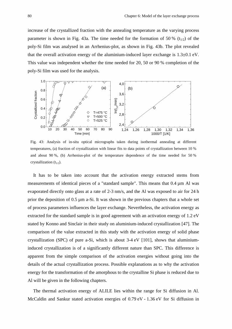
80 Chapter 6: Model of the layer exchange process
increase of the crystallized fraction with the annealing temperature as the varying process
parameter is shown in Fig. 43a. The time needed for the formation of 50 % (t1/2) of the
poly-Si film was analysed in an Arrhenius-plot, as shown in Fig. 43b. The plot revealed
that the overall activation energy of the aluminium-induced layer exchange is 1.3±0.1 eV.
This value was independent whether the time needed for 20, 50 or 90 % completion of the
poly-Si film was used for the analysis.
It has to be taken into account that the activation energy extracted stems from
measurements of identical pieces of a "standard sample". This means that 0.4 µm Al was
evaporated directly onto glass at a rate of 2-3 nm/s, and the Al was exposed to air for 24 h
prior the deposition of 0.5 µm a-Si. It was shown in the previous chapters that a whole set
of process parameters influences the layer exchange. Nevertheless, the activation energy as
extracted for the standard sample is in good agreement with an activation energy of 1.2 eV
stated by Konno and Sinclair in their study on aluminium-induced crystallization [47]. The
comparison of the value extracted in this study with the activation energy of solid phase
crystallization (SPC) of pure a-Si, which is about 3-4 eV [101], shows that aluminium-
induced crystallization is of a significantly different nature than SPC. This difference is
apparent from the simple comparison of the activation energies without going into the
details of the actual crystallization process. Possible explanations as to why the activation
energy for the transformation of the amorphous to the crystalline Si phase is reduced due to
Al will be given in the following chapters.
The thermal activation energy of ALILE lies within the range for Si diffusion in Al.
McCaldin and Sankur stated activation energies of 0.79 eV - 1.36 eV for Si diffusion in
1,24 1,26 1,28 1,30 1,32 1,34 1,36
2,4
2,8
3,2
3,6
4,0
ln(t
1/2/
min
)
1000/T [1/K]
(a) (b)
10 20 30 40 50 60 70 80 900.0
0.2
0.4
0.6
0.8
1.0
T=475 °C T=500 °C T=525 °C
Cry
stal
lized
frac
tion
Time [min]
Fig. 43: Analysis of in-situ optical micrographs taken during isothermal annealing at different
temperatures, (a) fraction of crystallization with linear fits to data points of crystallization between 10 %
and about 90 %, (b) Arrhenius-plot of the temperature dependence of the time needed for 50 %
crystallization (t1/2).
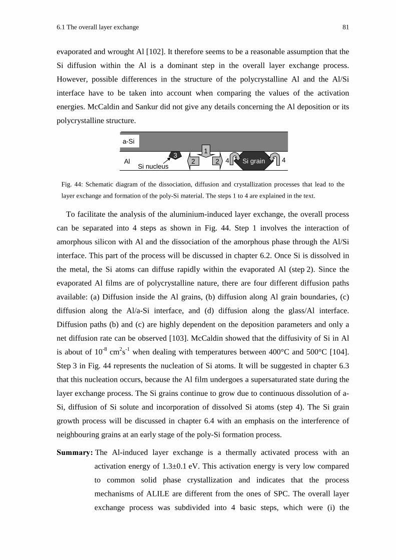
6.1 The overall layer exchange 81
evaporated and wrought Al [102]. It therefore seems to be a reasonable assumption that the
Si diffusion within the Al is a dominant step in the overall layer exchange process.
However, possible differences in the structure of the polycrystalline Al and the Al/Si
interface have to be taken into account when comparing the values of the activation
energies. McCaldin and Sankur did not give any details concerning the Al deposition or its
polycrystalline structure.
To facilitate the analysis of the aluminium-induced layer exchange, the overall process
can be separated into 4 steps as shown in Fig. 44. Step 1 involves the interaction of
amorphous silicon with Al and the dissociation of the amorphous phase through the Al/Si
interface. This part of the process will be discussed in chapter 6.2. Once Si is dissolved in
the metal, the Si atoms can diffuse rapidly within the evaporated Al (step 2). Since the
evaporated Al films are of polycrystalline nature, there are four different diffusion paths
available: (a) Diffusion inside the Al grains, (b) diffusion along Al grain boundaries, (c)
diffusion along the Al/a-Si interface, and (d) diffusion along the glass/Al interface.
Diffusion paths (b) and (c) are highly dependent on the deposition parameters and only a
net diffusion rate can be observed [103]. McCaldin showed that the diffusivity of Si in Al
is about of 10-8 cm2s-1 when dealing with temperatures between 400°C and 500°C [104].
Step 3 in Fig. 44 represents the nucleation of Si atoms. It will be suggested in chapter 6.3
that this nucleation occurs, because the Al film undergoes a supersaturated state during the
layer exchange process. The Si grains continue to grow due to continuous dissolution of a-
Si, diffusion of Si solute and incorporation of dissolved Si atoms (step 4). The Si grain
growth process will be discussed in chapter 6.4 with an emphasis on the interference of
neighbouring grains at an early stage of the poly-Si formation process.
' The Al-induced layer exchange is a thermally activated process with an
activation energy of 1.3±0.1 eV. This activation energy is very low compared
to common solid phase crystallization and indicates that the process
mechanisms of ALILE are different from the ones of SPC. The overall layer
exchange process was subdivided into 4 basic steps, which were (i) the
a-Si
Al
1
2 Si grain 4423
Si nucleus
Fig. 44: Schematic diagram of the dissociation, diffusion and crystallization processes that lead to the
layer exchange and formation of the poly-Si material. The steps 1 to 4 are explained in the text.
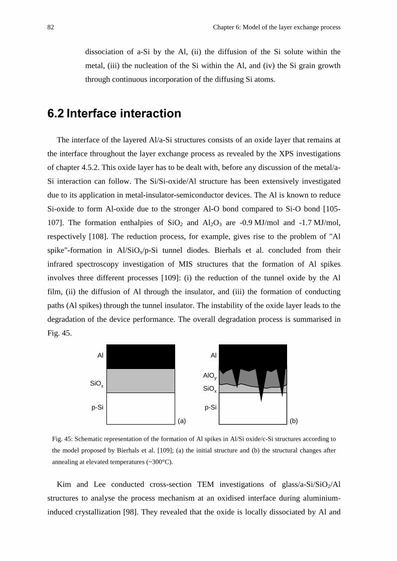
82 Chapter 6: Model of the layer exchange process
dissociation of a-Si by the Al, (ii) the diffusion of the Si solute within the
metal, (iii) the nucleation of the Si within the Al, and (iv) the Si grain growth
through continuous incorporation of the diffusing Si atoms.
4
The interface of the layered Al/a-Si structures consists of an oxide layer that remains at
the interface throughout the layer exchange process as revealed by the XPS investigations
of chapter 4.5.2. This oxide layer has to be dealt with, before any discussion of the metal/a-
Si interaction can follow. The Si/Si-oxide/Al structure has been extensively investigated
due to its application in metal-insulator-semiconductor devices. The Al is known to reduce
Si-oxide to form Al-oxide due to the stronger Al-O bond compared to Si-O bond [105-
107]. The formation enthalpies of SiO2 and Al2O3 are -0.9 MJ/mol and -1.7 MJ/mol,
respectively [108]. The reduction process, for example, gives rise to the problem of "Al
spike"-formation in Al/SiOx/p-Si tunnel diodes. Bierhals et al. concluded from their
infrared spectroscopy investigation of MIS structures that the formation of Al spikes
involves three different processes [109]: (i) the reduction of the tunnel oxide by the Al
film, (ii) the diffusion of Al through the insulator, and (iii) the formation of conducting
paths (Al spikes) through the tunnel insulator. The instability of the oxide layer leads to the
degradation of the device performance. The overall degradation process is summarised in
Fig. 45.
Kim and Lee conducted cross-section TEM investigations of glass/a-Si/SiO2/Al
structures to analyse the process mechanism at an oxidised interface during aluminium-
induced crystallization [98]. They revealed that the oxide is locally dissociated by Al and
SiOx
p-Si
Al
(a)
SiOx
p-Si
Al
AlOy
(b)
Fig. 45: Schematic representation of the formation of Al spikes in Al/Si oxide/c-Si structures according to
the model proposed by Bierhals et al. [109]; (a) the initial structure and (b) the structural changes after
annealing at elevated temperatures (~300°C).
6.2 Interface interaction 83
proposed that, on one hand, Al2O3 was formed, and, on the other hand, Si-Al intermixed
phases developed at these local sites. The interface oxide can therefore not be treated as a
continuous and homogenous layer. It acts rather like a membrane that allows the local
interaction of the metal and the amorphous silicon due to the reduction of the oxide and the
formation of Al spikes. The oxide itself is known to be a successful diffusion barrier [110].
Although the discussion, so far, concerns glass/a-Si/Al structures, where a Si oxide layer
initially separates the two films, the hypothesis of an inhomogeneous oxide layer can be
extended to glass/Al/a-Si structures with an Al oxide at the interface. The fact that in both
types of structures a layer exchange occurs proves that an interaction of the Al and a-Si
layers is possible independent of the initial type of interface oxide.
Ottaviani and Majni studied the influence of an Al oxide layer on solid phase epitaxy of
amorphous silicon onto crystalline Si wafers [111]. They suggested that the oxide layer
acted as a diffusion barrier on the Al atoms, but allowed the Si atoms to diffuse into the
metal layer with subsequent crystallization. However, they did not investigate where the Al
oxide layer is located after the SPE process. Their model of a one-way diffusion barrier is
not in agreement with the results presented in this study. Based on the XPS measurements
in chapter 4.5.2, strong evidence is given that the Al oxide remains at the interface and that
a migration of Al and Si material in opposite directions is possible in spite of the interface
oxide. Consequently, the oxide layer ought to consist of a structure that allows this material
transport to happen. An inhomogeneous membrane-like structure is therefore suggested for
the Al oxide interface layer.
As mentioned previously, the diffusion of the Si atoms through the metal of a simple
eutectic metal/Si system and subsequent crystallization have widely been accepted as the
basic processes of metal-induced crystallization. Nevertheless, little is known about the
actual dissociation mechanism of the amorphous silicon by the metal. The overall driving
force behind the crystallization process is the reduction of Gibbs energy by the
transformation of amorphous to crystalline silicon (~0.1 eV/atom [19]). However, the
covalent Si-Si bond is relatively strong with about 2 eV per bond. The overall activation
energy of solid phase crystallization (SPC) of pure a-Si material is therefore high with
about 3-4 eV [101]. This causes the formation of poly-Si by SPC to be slow even at
temperatures above 600°C [86]. In contrast, the crystallization of a-Si when in contact with
Al occurs at much lower temperatures, is faster, and has a lower activation energy. The
reported activation energy for Al-induced crystallization varies between 0.8 eV and 1.2 eV
as stated by Qingheng et al. according to their measurement on solid phase epitaxy [112]
84 Chapter 6: Model of the layer exchange process
and Konno and Sinclair in their study on Al/a-Si multilayer interaction [47], respectively.
The activation energy for the aluminium-induced layer exchange process is 1.3 eV as
determined in the previous chapter.
The question is therefore, how the metal reduces the energy required to break the Si-Si
bonds prior to any diffusion process. There are two main models that propose a
dissociation mechanism of the amorphous silicon in spite of the covalent Si bonding: (i)
Tu’s “interstitial model” [113] and (ii) Hiraki’s “screening model” [114]. Tu’s model is
based on an initial intermixing of the metal and the Si atoms at the interface. It is proposed
that the metal atoms into the Si, forming metal interstitials. These interstitial defects
in the Si structure are expected to considerably change the nature of the neighbouring Si-Si
bonds. The covalent bonds will no longer remain in their localised state. The metal
interstitial therefore induces the conversion from the covalent Si-Si bond of the
neighbouring Si atoms to a non-covalent bond. This altered bond is weaker than a saturated
covalent bond. Tu argues that the Si atoms can dissociate themselves from the lattice at a
reduced activation energy and diffuse into the metal. However, the initial formation of the
metal interstitials is not specified as such. Although Tu suggested his model for silicide
forming metal/Si interfaces (Ni-Si, Pd-Si and Pt-Si), the interstitial model was also adapted
to explain studies on metal/a-Si interfaces of simple eutectic systems, e.g. the Au/Si [36]
and the Al/Si-system [115].
Hiraki’s screening model, on the other hand, does not rely on unspecified initial
jumping of metal atoms into the Si structure. He postulates that the weakening of the
covalent Si-Si bonds at the metal/Si interface is due to the ability of the metal to screen the
Coulomb interaction by its mobile free electrons. This screening effect results in a
transition of non-metal to metal-like bonding of the adjacent semiconductor material over
the region of a few monolayers at the interface [116]. This region is characterised by the
formation of a nearly uniform electron gas. The valence electrons of the Si in this region
are not associated with specific atoms anymore. Hiraki’s model is based on calculations by
Inkson and Anderson on the band closure of the energy band gap of covalent
semiconductors applying many-body techniques to interface calculations [117,118]. The
arguments of the band closure are also supported by the analysis of Okiji et al. [119], who
concluded that the covalent non-metallic state of an insulator became metallic due to band
gap closure at the insulator/metal interface.
6.2 Interface interaction 85
The atomic mobility in a covalent semiconductor is low compared to the mobility in
metals. The resistance against atomic motion in metals is predominantly due to atomic size
effects and the crystallographic structure of the films (defects, grain boundaries and so on).
The electron gas of a metallic-like compound does not restrict the atomic motion as
strongly as the electron configuration of a covalent semiconductor material. The atoms of a
metallic-like, transformed semiconductor region near the metal interface are therefore
more mobile than atoms of the bulk area.
Hiraki’s screening model is strongly supported by the analysis of monolayer by
monolayer growth of Au onto clean silicon surfaces. The results reveal that a critical Au
layer thickness (4 monolayers) has to be deposited, before any interface reaction between
Si and the metal occurs [114,116]. If the Au layer is thinner than the critical thickness, it
acts rather like a non-metal than a metal. Even during the heating of 1-2 monolayer thick
Au films up to 800°C, the metal does not react with the adjacent Si material. However, an
Au layer thicker than the critical thickness already reacts at room temperature with Si. The
first couple of metal layers on the Si surface are bonded in a covalent rather than a metallic
way [120]. In thicker Au layers (>3 monolayers) the metallic free electron system can
establish and, consequently, induce instability of the covalent Si-Si bonding mentioned
above. Evidence for a critical metal layer thickness to induce crystallization was also given
by Radnoczi et al. [121]. They showed that a minimal Al layer thickness (3 or more
monolayers) is mandatory to cause crystallization of a-Si at a temperature of about 170°C.
Once the dissociation process of the amorphous silicon material is facilitated, an
exothermic intermixing process can take place. Walser and Bené suggested that at the
immediate interface a is formed [122], which reduces the energy of the
interface system faster [123]. The metallic glass is seen as a transition phase before any
silicide formation occurs. Even for simple eutectic systems such as the Al/Si and Au/Si
some evidence has been given that a metastable metal silicide is formed near the interface
prior to any nucleation of crystalline Si [36,41,124,125]. Ashtikar and Sharma showed that
the metastable Al silicide decomposes completely at temperatures above 300°C [41].
However, Konno and Sinclair did not find any evidence of silicide or liquid phase
formation prior to the diffusion of the Si atoms into the Al and subsequent crystallization
[47]. They conducted in-situ TEM-investigations of the crystallization of silicon in Al/a-Si
multilayer systems at 200°C. Thus, the initial reaction between metal and a-Si at the
interface is still controversially discussed.
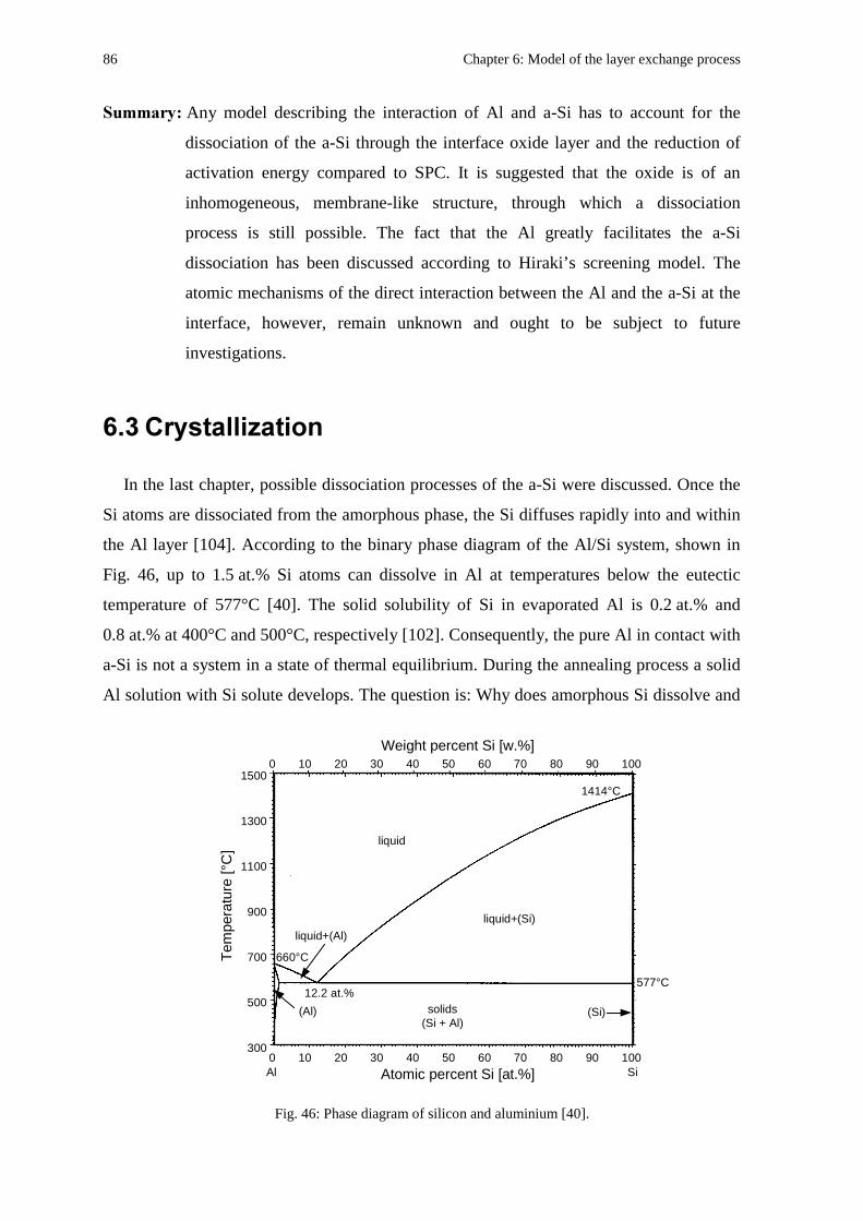
86 Chapter 6: Model of the layer exchange process
' Any model describing the interaction of Al and a-Si has to account for the
dissociation of the a-Si through the interface oxide layer and the reduction of
activation energy compared to SPC. It is suggested that the oxide is of an
inhomogeneous, membrane-like structure, through which a dissociation
process is still possible. The fact that the Al greatly facilitates the a-Si
dissociation has been discussed according to Hiraki’s screening model. The
atomic mechanisms of the direct interaction between the Al and the a-Si at the
interface, however, remain unknown and ought to be subject to future
investigations.
4&
In the last chapter, possible dissociation processes of the a-Si were discussed. Once the
Si atoms are dissociated from the amorphous phase, the Si diffuses rapidly into and within
the Al layer [104]. According to the binary phase diagram of the Al/Si system, shown in
Fig. 46, up to 1.5 at.% Si atoms can dissolve in Al at temperatures below the eutectic
temperature of 577°C [40]. The solid solubility of Si in evaporated Al is 0.2 at.% and
0.8 at.% at 400°C and 500°C, respectively [102]. Consequently, the pure Al in contact with
a-Si is not a system in a state of thermal equilibrium. During the annealing process a solid
Al solution with Si solute develops. The question is: Why does amorphous Si dissolve and
300
500
700
900
1100
1300
1500
0 10 20 30 40 50 60 70 80 90 100
0 10 20 30 40 50 60 70 80 90 100
12.2 at.%
660°C
1414°C
Tem
pera
ture
[°C
]
Atomic percent Si [at.%]
Weight percent Si [w.%]
(Al) (Si)
liquid
solids(Si + Al)
liquid+(Si)
liquid+(Al)
Al Si
Fig. 46: Phase diagram of silicon and aluminium [40].
577°C
6.3 Crystallization 87
yet stable crystalline silicon grow from this solution? The reason for this one-way action of
taking the amorphous phase completely apart and putting it back together in a crystalline
form could be that the Al undergoes a state of Si supersaturation during the crystallization
process. The possibility of this explanation is analysed in the following discussion, which
is an extension of Konno and Sinclair’s analysis of multilayer systems consisting of
stacked, 6 nm thin Al and a-Si films [47].
The reason for a supersaturated Al solution lies in the difference in Gibbs energy, G, of
the stable crystalline compared to the metastable amorphous silicon phase. To elaborate in
more detail on the circumstances of this supersaturation, the partial molar Gibbs energy, gi,
of a component i will be used. gi is also known as the chemical potential, µi, and is defined
as [126]:
jn,p,Tii n
Gg
∂∂=
(11)
where nj is the number of moles of component j≠i, T the temperature and p the pressure. In
this discussion Si is the only component of interest, the index i will therefore be dropped
from now on. The difference of the amorphous to the crystalline Si phase can be expressed
in terms of excess Gibbs energy:
gE = ga-Si – gc-Si = hE – TsE (12)
with ga-Si and gc-si being the molar Gibbs energies of the amorphous and the crystalline
phase, respectively. hE is the molar excess enthalpy and sE the molar excess entropy. The
excess Gibbs energy is related to the activity, a, as follows [126]:
gE = RT ln a (13)
where R is the molar gas constant. Using equations (12) and (13) the activity can be
calculated when hE and sE are known quantities. The molar excess enthalpy of a-Si in
relation to c-Si can be taken as the enthalpy of crystallization, measured by Dononvan et
al. to be 11.9 kJ/mol [127]. The excess entropy was determined by Spaepen to be
1.66 J/(mol K) [128]. Using these values, the activity of a-Si relative to crystalline silicon
as the standard state can be calculated to be 6 at 475°C. The activity can now be used to
estimate a possible supersaturation of Al with Si solute when in contact with a-Si. For this,
the Al/a-Si system is hypothetically regarded to be in thermal equilibrium omitting any Si
nucleation.
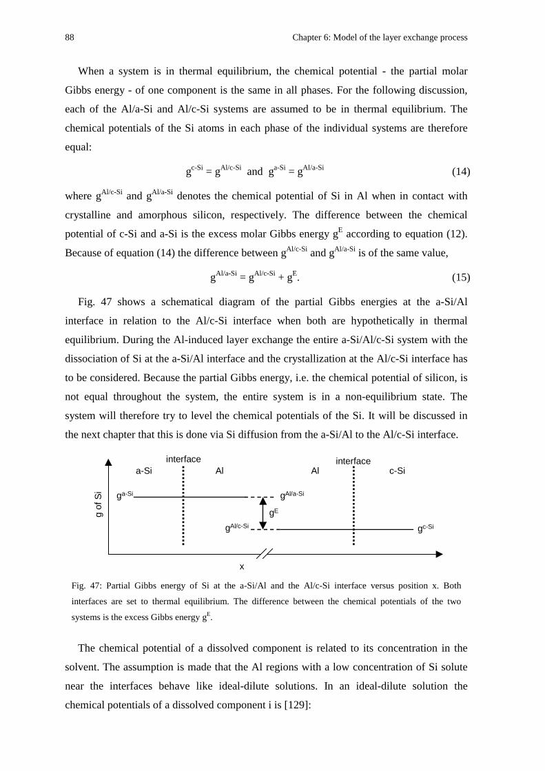
88 Chapter 6: Model of the layer exchange process
When a system is in thermal equilibrium, the chemical potential - the partial molar
Gibbs energy - of one component is the same in all phases. For the following discussion,
each of the Al/a-Si and Al/c-Si systems are assumed to be in thermal equilibrium. The
chemical potentials of the Si atoms in each phase of the individual systems are therefore
equal:
gc-Si = gAl/c-Si and ga-Si = gAl/a-Si (14)
where gAl/c-Si and gAl/a-Si denotes the chemical potential of Si in Al when in contact with
crystalline and amorphous silicon, respectively. The difference between the chemical
potential of c-Si and a-Si is the excess molar Gibbs energy gE according to equation (12).
Because of equation (14) the difference between gAl/c-Si and gAl/a-Si is of the same value,
gAl/a-Si = gAl/c-Si + gE. (15)
Fig. 47 shows a schematical diagram of the partial Gibbs energies at the a-Si/Al
interface in relation to the Al/c-Si interface when both are hypothetically in thermal
equilibrium. During the Al-induced layer exchange the entire a-Si/Al/c-Si system with the
dissociation of Si at the a-Si/Al interface and the crystallization at the Al/c-Si interface has
to be considered. Because the partial Gibbs energy, i.e. the chemical potential of silicon, is
not equal throughout the system, the entire system is in a non-equilibrium state. The
system will therefore try to level the chemical potentials of the Si. It will be discussed in
the next chapter that this is done via Si diffusion from the a-Si/Al to the Al/c-Si interface.
The chemical potential of a dissolved component is related to its concentration in the
solvent. The assumption is made that the Al regions with a low concentration of Si solute
near the interfaces behave like ideal-dilute solutions. In an ideal-dilute solution the
chemical potentials of a dissolved component i is [129]:
gE
a-Si Al Al c-Si
x
g of
Si gAl/a-Si
gAl/c-Si
ga-Si
gc-Si
interface interface
Fig. 47: Partial Gibbs energy of Si at the a-Si/Al and the Al/c-Si interface versus position x. Both
interfaces are set to thermal equilibrium. The difference between the chemical potentials of the two
systems is the excess Gibbs energy gE.
6.3 Crystallization 89
gi = gi* + RT ln Xi (16)
where gi* is a standard chemical potential and Xi is the relative concentration of the solute.
Using equations (15) and (16), the following relationship for Si solute in a dilute Al
solution is obtained:
g* + RT ln XAl/c-Si + gE = g* + RT ln XAl/a-Si (17)
where XAl/c-Si and XAl/a-Si are the Si concentrations in Al when in contact with c-Si and a-Si,
respectively. From this equation in combination with equation (13) the two concentrations
can be related by the activity:
XAl/c-Si a = XAl/a-Si (18)
When the Al/c-Si system is in thermal equilibrium, the phase diagram determines the Si
concentration in the Al. The solid solubility of Si in Al at 475°C is about 0.5 at.% [130].
Since an activity of 6 has been calculated above, it can be determined that XAl/a-Si equals
3 at.% when using equation (18).
The conclusion from the above analysis is that if Al was not subject to a solid solubility
limit, meaning no nucleation could occur, the Si concentration of Al in contact with a-Si
would be 3 at.% when brought into thermal equilibrium at 475°C. This Si concentration
exceeds the maximal solid solubility of Si in Al as apparent from Fig. 46. Considering the
Al/c-Si system, the Al with such high Si concentration is in a supersaturated state. In
reality this supersaturation is released by nucleation and growth of crystalline silicon grains
within the Al. It is unknown whether a concentration of 3 at.% at 475°C, as an upper limit,
is reached or whether crystallization already takes place at a state of lower concentration.
Nevertheless, throughout the crystallization process the amorphous Si phase adds Si atoms
to the Al solution to increase the chemical potential of the Si solute, whilst the growing
crystalline Si phase is extracting Si to decrease this chemical potential. The aluminium is
therefore in a state of undersaturation in relation to the a-Si and a state of supersaturation in
relation to the c-Si. This difference serves as an explanation for the one-way action of
dissociation of a-Si and yet formation of c-Si.
Evidence was given in earlier chapters (e.g. Fig. 12 of chapter 4.1 and Fig. 34 of chapter
5.2) that at lower temperatures dendritic growth behaviour of the Si grains is prevalent. In
general, dendritic growth occurs when a system is in an unstable supersaturated state. In
this case the system does not necessarily transform to reach the state of lowest Gibbs
energy directly but it changes along the path that allows the fastest reduction in Gibbs
90 Chapter 6: Model of the layer exchange process
energy [123]. This is the reason why snowflakes are formed instead of small balls of ice.
Regarding the Al/a-Si system, it follows from equation (13) that the lower the annealing
temperature, the higher the activity of the Si atoms. Using equations (12) and (13), the
activity of Si at 400°C, for example, is 7. According to the analysis presented, the lower
the temperature the higher the supersaturation of the Al solution with Si solute. This state
of higher supersaturation only implies that the ratio of XAl/a-Si to XAl/c-Si is higher.
Quantitatively, XAl/a-Si is lower at 400°C (1.4 at.%) than at 475°C, since XAl/c-Si is only
0.2 at.% at the lower temperature [102]. This consequence of stronger supersaturation with
decreasing temperature is in agreement with the observation of enhanced dendritic growth
at lower temperatures and supports the model of a supersaturated transition state of the
solid Al solution during the aluminium-induced layer exchange.
The nucleation of Si from the supersaturated Al solution does not occur homogeneously
since the evaporated Al is of polycrystalline nature. The Al grain boundaries and the triple
junctions of grain boundaries with the Al/a-Si interface are sites of lower critical energy for
the nucleus formation than bulk Al. At these sites preferential Si nucleation occurs.
Evidence for the preferential nucleation was given in Fig. 7b of chapter 4.1, where a Si
nucleus at a Al grain boundary/a-Si interface was shown. Additionally, chapter 4.4
revealed the dependence of the Si nucleation rate on the Al grain size. The smaller the
grain size, thus, the higher the grain boundary density, the higher the Si nucleation rate.
The relationship between nucleation rate and grain boundary density is in agreement with
the standard theory on grain formation and growth [68].
' The dissociation of a-Si and the formation of crystalline Si grains are driven by
the difference between the chemical potentials of the two states. The
metastable state of a-Si when in contact with Al leads to a supersaturation of
the metal with Si atoms. Considering the Al as a solid solution, an upper limit
of Si concentration in the supersaturated state was calculated to be 3 at.% at
475°C. The supersaturation is released by the nucleation and growth of
crystalline Si. The difference between the chemical potentials at the a-Si/Al
and the Al/c-Si interfaces provides a constant driving force for the dissociation,
diffusion and crystallization process.
6.4 Si grain growth 91
4) *
The discussion presented so far addressed how Si atoms dissociate from a-Si into
aluminium and why Si atoms are transferred form the amorphous to the growing
crystalline Si phase. This chapter analyses the growth behaviour of large-grained poly-Si
material during the aluminium-induced layer exchange process.
When amorphous silicon is crystallized using solid phase crystallization, individual
grains grow until they impinge. Prior to the impingement the growing grains increase their
size independently from each other. The growth behaviour and the nucleation are not
affected by already existing grains. The same characteristics are valid for the
crystallization of Si from a liquid phase formed by laser crystallization. This is one of the
fundamental differences in the formation of poly-Si material via an aluminium-induced
layer exchange process. In chapter 4.1 (see Fig. 9 and Fig. 10) evidence was given that at
an early stage of the crystallization process, existing grains suppress the formation of new
nuclei. This suppression can be interpreted as an interference of growing grains with the Al
matrix, as will be explained in the following discussion.
To form crystalline Si thin-films, the ideal process would be the nucleation of one grain
that grows until the entire amorphous phase is transformed. Based on this idealisation, the
following general rule for the formation of large-grained poly-Si films can be derived: The
fewer nuclei are formed, the larger the grains can grow before impingement occurs.
The initial state of the Si solute in the Al solvent prior to any nucleation has to be
analysed, before the interference of Si grains at an early stage of the Al-induced layer
exchange can be discussed. It was argued in chapter 6.3 that, when Al is in contact with a-
Si at a temperature of 475°C, Si atoms can dissolve up to the supersaturation concentration
cs of about 3 at.% at the Al/a-Si interface according to thermodynamic considerations. The
dissolved Si atoms diffuse quickly into the Al matrix. The concentration profile c(x,t) of
the Si solute from the interface into the aluminium, dependent on the position x and the
time t, is determined by the diffusivity D as follows [68]:
⋅⋅−−=
tD2
xerf)cc(c)t,x(c 0ss
(19)
with c0 the Si concentration far away from the interface, and 'erf' stands for error function.
Equation (19) is the analytical solution of Fick's second law assuming that the diffusivity is
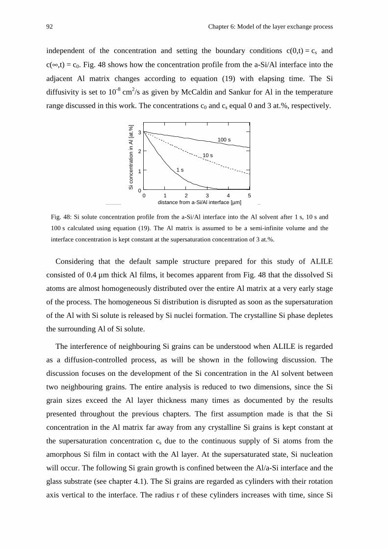
92 Chapter 6: Model of the layer exchange process
independent of the concentration and setting the boundary conditions c(0,t) = cs and
c(∞,t) = c0. Fig. 48 shows how the concentration profile from the a-Si/Al interface into the
adjacent Al matrix changes according to equation (19) with elapsing time. The Si
diffusivity is set to 10-8 cm2/s as given by McCaldin and Sankur for Al in the temperature
range discussed in this work. The concentrations c0 and cs equal 0 and 3 at.%, respectively.
Considering that the default sample structure prepared for this study of ALILE
consisted of 0.4 µm thick Al films, it becomes apparent from Fig. 48 that the dissolved Si
atoms are almost homogeneously distributed over the entire Al matrix at a very early stage
of the process. The homogeneous Si distribution is disrupted as soon as the supersaturation
of the Al with Si solute is released by Si nuclei formation. The crystalline Si phase depletes
the surrounding Al of Si solute.
The interference of neighbouring Si grains can be understood when ALILE is regarded
as a diffusion-controlled process, as will be shown in the following discussion. The
discussion focuses on the development of the Si concentration in the Al solvent between
two neighbouring grains. The entire analysis is reduced to two dimensions, since the Si
grain sizes exceed the Al layer thickness many times as documented by the results
presented throughout the previous chapters. The first assumption made is that the Si
concentration in the Al matrix far away from any crystalline Si grains is kept constant at
the supersaturation concentration cs due to the continuous supply of Si atoms from the
amorphous Si film in contact with the Al layer. At the supersaturated state, Si nucleation
will occur. The following Si grain growth is confined between the Al/a-Si interface and the
glass substrate (see chapter 4.1). The Si grains are regarded as cylinders with their rotation
axis vertical to the interface. The radius r of these cylinders increases with time, since Si
0 1 2 3 4 50
0.01
0.02
0.03
0.035
1 105−×
x 1, )
x 10, )
x 100, )
50 x
0
1
2
3
0 1 2 3 4 5distance from a-Si/Al interface [µm]
Si c
once
ntra
tion
in A
l [at
.%]
1 s
10 s
100 s
Fig. 48: Si solute concentration profile from the a-Si/Al interface into the Al solvent after 1 s, 10 s and
100 s calculated using equation (19). The Al matrix is assumed to be a semi-infinite volume and the
interface concentration is kept constant at the supersaturation concentration of 3 at.%.
6.4 Si grain growth 93
atoms near growing grains are incorporated into the advancing crystalline Si structure to
decrease their Gibbs energy. The incorporation is assumed to be fast in comparison to the
diffusion processes because of the incoherent interface between the Al matrix and the Si
crystal [131]. In the vicinity of the grains, the Si solute is therefore depleted and the
concentration ci of Si atoms at the Si grain/Al interface is lower than cs. Consequently, a
concentration gradient establishes from the c-Si/Al interface extending into the Al matrix.
This gradient induces the diffusion of Si solute towards the Si grains. The Si diffusion
within the Al matrix is the process mechanism that aims to equalise the chemical potentials
of the Si solute at the c-Si/Al and the Al/a-Si interfaces, presented in chapter 6.3.
Fig. 49 describes the development of the concentration profile between two
neighbouring grains that are growing towards each other with velocity v. The diagram of
Fig. 49a shows the situation at an early stage of the crystallization process. The grains are
still far apart, and if no additional nucleation occurs, the concentration between grain 1 and
2 is constant cs, except in the Si depletion regions near the interfaces. The concentration
profiles in these regions can be simplified using Zener’s one-dimensional linear gradient
approximation [132]. The concentration profile between grain 1 and 2, drawn as a solid
line in Fig. 49a, is based on this approximation. The Si solute concentration decreases from
cs to ci over a distance of the effective diffusion length L. Whilst the Si grains are growing,
the depletion regions are pushed further into the Al matrix (Fig. 49b). When the distance
between adjacent grains is finally smaller than twice the effective diffusion length, the
depletion regions begin to overlap (Fig. 49c). At this stage of the crystallization process the
concentration of Si solute between the adjacent grains decreases below cs, and the
possibility of further nuclei formation drops.
Thus, the Si grains growing within the Al matrix interfere via their Si depletion regions
before actual impingement of neighbouring grains occurs. This interference of isolated
grains at an early stage of ALILE leads to the suppression of new Si nuclei formation. The
fewer grains nucleate, the better for the growth of large-grained poly-Si, according to the
general rule of formation of large-grained material as stated above.
Since the Si concentration outside the depletion region is kept constant at cs due to the
continuous supply of Si atoms from the amorphous phase, it seems reasonable to assume
that a steady-state diffusion establishes between ci and cs. Under these conditions, in
conjunction with the assumption that the Al matrix is an isotropic medium, the Si
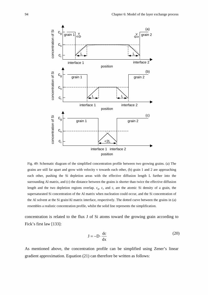
94 Chapter 6: Model of the layer exchange process
concentration is related to the flux J of Si atoms toward the growing grain according to
Fick’s first law [133]:
dx
dcDJ ⋅−=
(20)
As mentioned above, the concentration profile can be simplified using Zener’s linear
gradient approximation. Equation (21) can therefore be written as follows:
conc
entr
atio
n of
Si
cg
ci
cs
(a)
L L
interface 1 interface 2position
grain 1 grain 2v v
cg
ci
cs
(b)
L L
interface 1 interface 2position
grain 1 grain 2
(c)
<2L
interface 1 interface 2
position
grain 1 grain 2cg
ci
cs
conc
entr
atio
n of
Si
conc
entr
atio
n of
Si
Fig. 49: Schematic diagram of the simplified concentration profile between two growing grains. (a) The
grains are still far apart and grow with velocity v towards each other, (b) grain 1 and 2 are approaching
each other, pushing the Si depletion areas with the effective diffusion length L further into the
surrounding Al matrix, and (c) the distance between the grains is shorter than twice the effective diffusion
length and the two depletion regions overlap. cg, cs and ci are the atomic Si density of a grain, the
supersaturated Si concentration of the Al matrix when nucleation could occur, and the Si concentration of
the Al solvent at the Si grain/Al matrix interface, respectively. The dotted curve between the grains in (a)
resembles a realistic concentration profile, whilst the solid line represents the simplification.
6.4 Si grain growth 95
L
ccDJ is −
⋅−=(21)
On the other hand the flux of Si solute is related to the advancing c-Si/Al growth front due
to the conservation of Si atoms according to
vcJ g ⋅= (22)
with cg being the atomic density of crystalline silicon and v the growth velocity of the
radius of the Si grain. Using equations (21) and (22) the effective diffusion length L can be
calculated for a sample annealed at 475°C, analysed in chapter 4.1. The concentration ci at
the Al/c-Si interface is set equal to the solid solubility of Si in Al considering an Al/c-Si
system at 475°C (ci = 0.5 at.% [130]). The kinetic barrier between the growing crystalline
Si grain and the surrounding Al matrix is neglected because of the incoherent nature of the
interface. cs is the supersaturation concentration of Si in Al as determined for an Al/a-Si
system in the previous chapter and represents the upper limit. The atomic densities of Al
and Si are 6x1022 cm-3 and 5x1022 cm-3, respectively. The velocity v of the crystallization
front was determined in chapter 4.1 to be about 4.7 nm/s. Again using a diffusivity of
10-8 cm2/s, the effective diffusion length L is calculated to be about 6 µm. This means that
the depletion regions of two neighbouring grains begin to overlap when the distance
between their growth fronts is less than 12 µm.
According to the above model the formation of new Si nuclei is reduced when
overlapping of Si depletion regions commences. The nucleation rate should therefore
significantly decrease at this stage of the crystallization process. The nucleation rate is the
increase of the number of grains and can be extracted from the in-situ optical investigations
presented in chapter 4.1. The crystallization analysis was carried out using optical
micrographs before impingement of neighbouring grains occurred. Fig. 50 shows the
development of the grain density (filled squares) as extracted from the in-situ investigation
of a sample annealed at 475°C (see also Fig. 9 and Fig. 10, which are extracted from the
same set of data). Two time periods can be clearly distinguished. During the first period, at
times shorter than 35 min, the grain density increases rapidly. In the second period, at
times longer than 35 min, the grain density increases much more slowly and eventually
seems to saturate, although no impingement has yet occurred, and less than 40 % of the
poly-Si film has formed (see Fig. 10). The linear fits in both regions serve as guides to the
eye to highlight when the change of nucleation rate occurs. At this stage of the discussion,
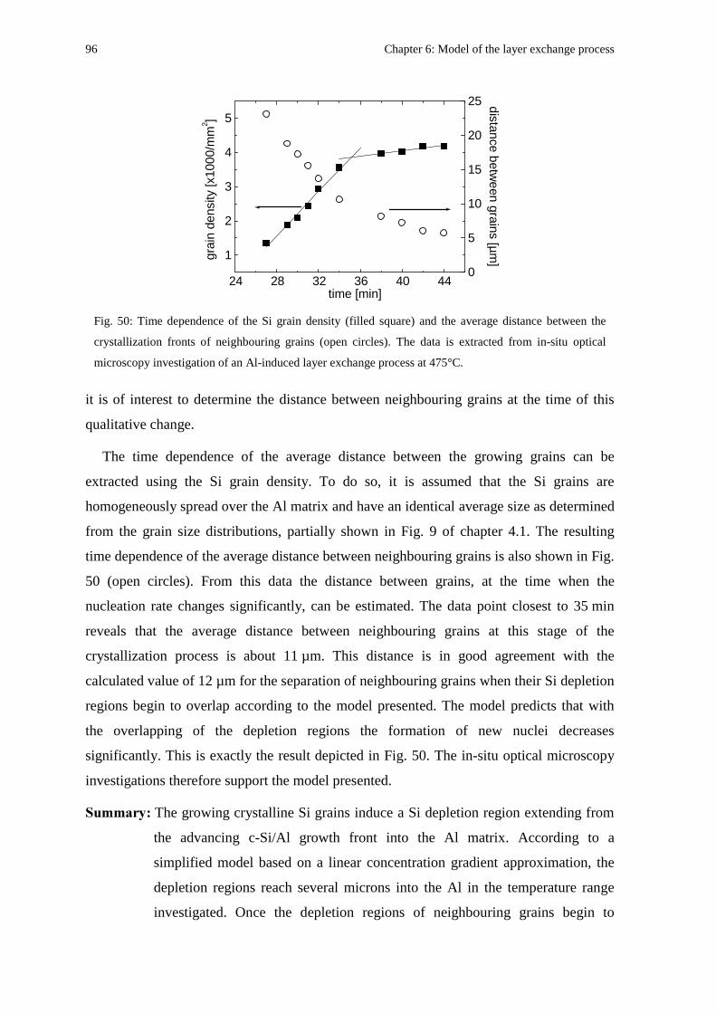
96 Chapter 6: Model of the layer exchange process
it is of interest to determine the distance between neighbouring grains at the time of this
qualitative change.
The time dependence of the average distance between the growing grains can be
extracted using the Si grain density. To do so, it is assumed that the Si grains are
homogeneously spread over the Al matrix and have an identical average size as determined
from the grain size distributions, partially shown in Fig. 9 of chapter 4.1. The resulting
time dependence of the average distance between neighbouring grains is also shown in Fig.
50 (open circles). From this data the distance between grains, at the time when the
nucleation rate changes significantly, can be estimated. The data point closest to 35 min
reveals that the average distance between neighbouring grains at this stage of the
crystallization process is about 11 µm. This distance is in good agreement with the
calculated value of 12 µm for the separation of neighbouring grains when their Si depletion
regions begin to overlap according to the model presented. The model predicts that with
the overlapping of the depletion regions the formation of new nuclei decreases
significantly. This is exactly the result depicted in Fig. 50. The in-situ optical microscopy
investigations therefore support the model presented.
' The growing crystalline Si grains induce a Si depletion region extending from
the advancing c-Si/Al growth front into the Al matrix. According to a
simplified model based on a linear concentration gradient approximation, the
depletion regions reach several microns into the Al in the temperature range
investigated. Once the depletion regions of neighbouring grains begin to
24 28 32 36 40 44
1
2
3
4
5
grai
n de
nsity
[x10
00/m
m2 ]
time [min]
0
5
10
15
20
25 distance between grains [µm
]
Fig. 50: Time dependence of the Si grain density (filled square) and the average distance between the
crystallization fronts of neighbouring grains (open circles). The data is extracted from in-situ optical
microscopy investigation of an Al-induced layer exchange process at 475°C.
6.4 Si grain growth 97
overlap, the model predicts a significant change in the nucleation rate. This
change was found in the analysis of in-situ optical investigations. It occurs
when the average distance between neighbouring grains is about 11 µm for a
sample annealed at 475°C. This value is in good agreement with the predicted
value of 12 µm. The interference of grains via their Si depletion regions leads
to the suppression of new nuclei formation at an early stage of the layer
exchange process, the prerequisite for the growth of large-grained poly-Si
films. Thus, the model presented successfully explains why the Al-induced
layer exchange process can lead to the formation of poly-Si films with grain
sizes exceeding 10 µm.
4,5
In the last chapters, a model of the aluminium-induced layer exchange was developed
by analysing the individual process steps of the a-Si dissociation, the crystallization and the
Si grain growth. In this chapter, the model will be critically discussed taking some of the
results presented in chapters 4 and 5 into consideration. Table 5 lists some of the process
parameters that influence the grain size of the poly-Si films formed during ALILE as well
as the overall crystallization velocity. These parameters will be related to the model of
ALILE. Additionally, the thermodynamic reasoning for the one-way process of a-Si
dissociation and yet c-Si formation, presented in chapter 6.3, will be discussed.
.
Annealing temperature ⇑ ⇓ ⇑ 4.3
Al grain size ⇑ ⇑ ⇓ 4.4
interface oxide ⇑ ⇑ ⇓ 4.5.1
Table 5: List of process parameters that influence the grain size and the crystallization velocity. The
arrow ⇑ indicates an increase in annealing temperature, grain size of the polycrystalline Al or the
thickness of the interface oxide, as well as an increase in grain size of the poly-Si and the
crystallization process velocity. The arrow ⇓ indicates the opposite.
In chapter 4.5.3 it is shown that no Al/Si layer exchange occurs without an interface
oxide, although crystallization is induced by the Al. This highlights the point that an oxide
layer between the Al and a-Si layers is a mandatory requirement for the successful layer
exchange. However, little is still known about the role of the interface oxide. To achieve a
98 Chapter 6: Model of the layer exchange process
better insight, the structure of this interface layer has to be investigated using cross-section
high resolution TEM, for example. To study the role of Al and/or Si oxide interfaces
efficiently, the Al, the oxide and the a-Si layers should be deposited under well-defined
conditions in an integrated deposition system. Such an experimental set-up could provide
important details concerning the interface oxide as process parameter and regulator of
ALILE.
In chapter 4.5.1 it was shown that the thicker the interface oxide, the larger the Si
grains, but the slower the crystallization process. The oxide influences the initial
interaction of the Al and the a-Si. Before any interaction can occur, diffusion paths through
the interface oxide have to develop. A thicker oxide therefore decelerates the overall
crystallization process. When a-Si dissociation through the membrane-like oxide occurs,
followed by Si diffusion, grains can finally form within the Al. These grains deplete the
surrounding Al solvent of Si solute. In the model presented, the Si concentration outside
the effective diffusion regions is kept constant due to the continuous supply of Si from the
a-Si. It is assumed that a steady-state diffusion between cs and ci establishes. However, if a
thicker interface oxide hampers the Si supply, this steady state condition might not
develop, and the effective diffusion length L of the Si grains keeps on increasing until
neighbouring depletion regions begin to overlap. In this case, a time dependent description
of L ought to be incorporated into the model.
In chapter 6.3, the difference of chemical potentials at the a-Si/Al and the Al/c-Si
interfaces was suggested as the driving force for the one-way process of a-Si dissociation
and crystallization of Si grains. However, even crystalline Si wafer are partially dissolved
when in contact with Al [109]. Si is dissolved up to the solid solubility limit of the Al/c-Si
system. Magee and Peng’s study on the interaction of polycrystalline Al in contact with
crystalline silicon showed that the dissolved silicon crystallized at the Al grain boundaries
[134]. It has already been mentioned that Al grain boundaries are preferential nucleation
sites. The grain boundaries could be regarded as sites where Si supersaturation locally
occurs within the polycrystalline Al structure, although the Al grains themselves are not
supersaturated. The thermodynamic description presented in chapter 6.3 for an a-Si/Al/c-Si
system seems to be unsuited to discuss the interaction of Al with crystalline Si. A
description would have to be developed that took the inhomogeneous crystallographic
structure of evaporated Al into consideration. This description could then be extended and
incorporated into a model of ALILE.
6.5 Discussion 99
The model of the formation of large-grained poly-Si is based on the simplified, one-
dimensional linear gradient profile of the Si concentration in Al. The assumption is made
that there is a steady-state diffusion between the supersaturation concentration cs and the
Al/Si grain interface concentration ci. cs is the upper limit of the Si solute in Al. This
concentration was extracted using the activity differences of Si atoms in the Al/a-Si and the
Al/c-Si systems. For the particular set of samples analysed in chapter 6.4, cs was
determined to be 6 times as large as the Si concentration in Al when in thermal equilibrium
with c-Si. However, Si crystallization becomes likely to occur as soon as the solid
solubility limit of Al is exceeded, which is below cs. The model therefore implies that the
a-Si dissociation and Si diffusion is fast compared to the nucleation, and the high activity
of Si in the a-Si/Al system practically the Si atoms into the Al up to a
supersaturation concentration cs as the upper limit. ci, on the other hand, is taken as the
solid solubility concentration of the Al/c-Si system. It represents the lower Si concentration
limit at the interface, since the time needed for the incorporation process of the Si atoms
form the Al solution into the crystalline Si phase is neglected. Under these circumstances
the growth process is entirely diffusion controlled [68]. However, if the interface kinetics
cannot be neglected, the process is mixed controlled by diffusion and interface reactions,
and the concentration at the interface would be higher. Directly measured values for both
concentrations, cs and ci, would consequently allow a more detailed analysis of the overall
aluminium-induced layer exchange. The difficulty is that the measurements would have to
be time-dependent, in-situ and with high spatial resolution.
In chapter 6.4, the formation of large-grain poly-Si is related to the interference of the Si
depletion regions surrounding neighbouring grains. It is proposed that this interference
leads to the suppression of further Si nucleation. The quantitative analysis of this
interference process is dependent on the Si concentration profile within the Al matrix. The
model presented uses the approximation of a linear gradient profile of the Si concentration
inside the Si depletion regions. The model could therefore be improved by applying a more
sophisticated description of the concentration profile. Allen et al. have investigated the
interaction of microcrystalline Si in contact with a thin-film of Au [49]. They developed a
model for the concentration profile that was based on the continuity equation, relating the
dissolution of Si to the diffusion and growth of stable Si grains within the metal layer. The
effective diffusion length L in their model was set equal to B/Dd ⋅ , with d being the
metal layer thickness, D the diffusivity and B the dissolution rate of the microcrystalline Si
in contact with Au. Scranton and McCaldin conducted studies on the dissolution rate of
100 Chapter 6: Model of the layer exchange process
amorphous silicon in contact with evaporated Al [103], however, their published values
scatter significantly. It seems that there are no more reliable values of the dissolution rate
of amorphous Si into Al available, as yet. The adaptation of Allen and co-workers’ more
sophisticated Si concentration profile to ALILE does therefore not improve the model in a
way that it could be related to experimental results in a non-ambiguous way.
In chapter 4.3 it was shown that the grain size of the poly-Si films is temperature
dependent: The lower the annealing temperature, the larger the grain size. The grain size of
polycrystalline material is determined by the competing processes of nucleation and grain
growth, as discussed chapter 6.4. From the analysis of ALILE, it seems that the nucleation
rate decreases more strongly than the Si grain growth velocity with decreasing
temperature, which explains the reciprocal dependence of grain size and annealing
temperature. In chapter 6.1, the activation energy of the thermally activated Al-induced
layer exchange process was determined to be 1.3 eV. To discuss the temperature
dependence of the Si grain size quantitatively, it would be necessary to separate this
overall activation energy into the activation energies of nucleation and grain growth. The
requirement for that is the independent observation of both processes. However, existing
grains suppress the formation of new Si nuclei at an early stage of the crystallization
process, as was shown in chapter 4.1. Extracting an independent activation energy for the
nucleation rate is therefore difficult. A better in-situ optical microscopy system, than the
system available in this study, would be required. The system used only had a
magnification of 100. With a higher magnification, the Si grain growth process could be
observed at a stage before significant interference of neighbouring grains occurred.
' The model developed in this work for the Al-induced layer exchange process is
separated into process steps concerning the dissociation of the a-Si, the Si
diffusion within the Al, the Si nucleation and the Si grain growth. Several ways
to refine this model have been highlighted in this chapter. The comprehensive
description of the overall layer exchange including its main sub-processes in
the previous chapters can be seen as the basis for further investigations
focusing on individual process mechanisms of ALILE.
101
6
%
The aluminium-induced layer exchange process enables the fabrication of large-grained
continuous poly-Si thin-films (ALILE poly-Si) on glass substrates at low temperatures as
shown throughout the previous chapters. In this chapter, it will be discussed how these
poly-Si layers can be incorporated into Si thin-film solar cell fabrication. The concepts that
will be presented point in various directions. This reflects that the use of ALILE for solar
cells is in the beginning stage, and there is enormous room for improvement. The default
structure investigated in this work led to poly-Si thin-films with a thickness of less than
0.5 µm. This chapter will therefore begin with the discussion of using these very thin films
as seeding layers for subsequent epitaxial growth. Since the large Si grains are of good
crystallographic quality, the possibility of using ALILE poly-Si as absorber layers is
addressed in the second part. All the investigations in this chapter rely completely on
experience and results of studies presented and discussed in the previous chapters. It is the
first step to applying ALILE in solar cell preparation.
6%77'
The seeding layer concept is based on the idea that a very thin large-grained poly-Si
film induces epitaxial growth when a thicker absorber layer of several µm in thickness is
deposited. Large-grained seeding layers are formed by transforming a-Si or µc-Si material
on foreign substrates to poly-Si utilising crystallization techniques. In the high-temperature
approach (T>550°C), zone melting recrystallization processes are common techniques
[17]. The epitaxial thickening can be carried out using liquid phase epitaxy [135], ion-
assisted deposition (IAD) [136] or chemical vapour deposition (CVD) [17], for example.
Efficiencies as high as 9.4 % have been reported [137].
102 Chapter 7: Al-induced layer exchange for thin-film solar cells
In the low-temperature approach, solid phase crystallization and laser crystallization are
the most commonly applied methods for processing seeding layers. The subsequent
thickening layer is deposited using CVD or IAD. For example, the company Kaneka
investigated laser crystallized poly-Si thin-films as seeding layers using plasma-enhanced
CVD for the subsequent deposition of the absorber layers [138,139]. In more recent
publications, it seems, however, that the seeding layer concept was dropped. Cross-section
TEM investigations indicated that Kaneka’s laser crystallized poly-Si films did not induce
epitaxial growth [138]. The absorber layers are now grown onto an unspecified back
reflector [14,140]. One of the main obstacles of the seeding layer concept is that epitaxial
Si growth preferentially occurs on crystalline silicon with (100) orientation [85]. However,
SPC and LC lead to poly-Si thin-films with no texturing or preferred (111) orientation
[83,84]. In contrast, poly-Si formed by aluminium-induced layer exchange exhibits a (100)
texturing as shown in chapter 5.2. This effect in conjunction with large grain sizes makes
ALILE poly-Si films an interesting candidate for seeding layers.
The seeding layer concept is applicable for either superstrate or substrate cell
configurations. In a superstrate solar cell, the actual diode is illuminated through the glass.
Consequently, a front contact on the glass is needed prior to any film deposition. Thin
conducting oxides (TCO) commonly serve this purpose. Since the TCO is the first layer
deposited, all following processing steps have to be compatible with the maximum
temperature this layer can be exposed to.
The Al-induced layer exchange of a glass/Al/a-Si structure leads to the formation of a
poly-Si film directly on glass (see Fig. 3c of chapter 2.2). If the glass was initially covered
with a TCO, the structure could be used for subsequent superstrate cell fabrication. Since
the poly-Si films are highly Al doped, the solar cell structures deposited could either be
superstrate/TCO/p+-Si/i-Si/n-Si/back contact or superstrate/TCO/p+-Si/n-Si/back contact.
In both cases the main concern would be how much the TCO is effected by annealing
temperatures of 400°C to 500°C and/or whether interaction with the Al occurs, which is
initially adjacent to the TCO. These difficulties can be avoided when a substrate
configuration is utilised. In this configuration the solar cell is illuminated from the top and
the glass substrate serves as a mere carrier. The front contact TCO is the last layer
deposited. The temperature sensitivity of this film does therefore not hamper the previous
layer depositions. Nevertheless, a back contact has to be incorporated between the glass
substrate and the ALILE poly-Si film.
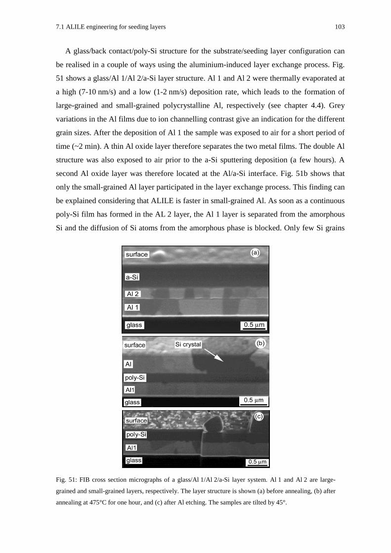
7.1 ALILE engineering for seeding layers 103
A glass/back contact/poly-Si structure for the substrate/seeding layer configuration can
be realised in a couple of ways using the aluminium-induced layer exchange process. Fig.
51 shows a glass/Al 1/Al 2/a-Si layer structure. Al 1 and Al 2 were thermally evaporated at
a high (7-10 nm/s) and a low (1-2 nm/s) deposition rate, which leads to the formation of
large-grained and small-grained polycrystalline Al, respectively (see chapter 4.4). Grey
variations in the Al films due to ion channelling contrast give an indication for the different
grain sizes. After the deposition of Al 1 the sample was exposed to air for a short period of
time (~2 min). A thin Al oxide layer therefore separates the two metal films. The double Al
structure was also exposed to air prior to the a-Si sputtering deposition (a few hours). A
second Al oxide layer was therefore located at the Al/a-Si interface. Fig. 51b shows that
only the small-grained Al layer participated in the layer exchange process. This finding can
be explained considering that ALILE is faster in small-grained Al. As soon as a continuous
poly-Si film has formed in the AL 2 layer, the Al 1 layer is separated from the amorphous
Si and the diffusion of Si atoms from the amorphous phase is blocked. Only few Si grains
Fig. 51: FIB cross section micrographs of a glass/Al 1/Al 2/a-Si layer system. Al 1 and Al 2 are large-
grained and small-grained layers, respectively. The layer structure is shown (a) before annealing, (b) after
annealing at 475°C for one hour, and (c) after Al etching. The samples are tilted by 45°.
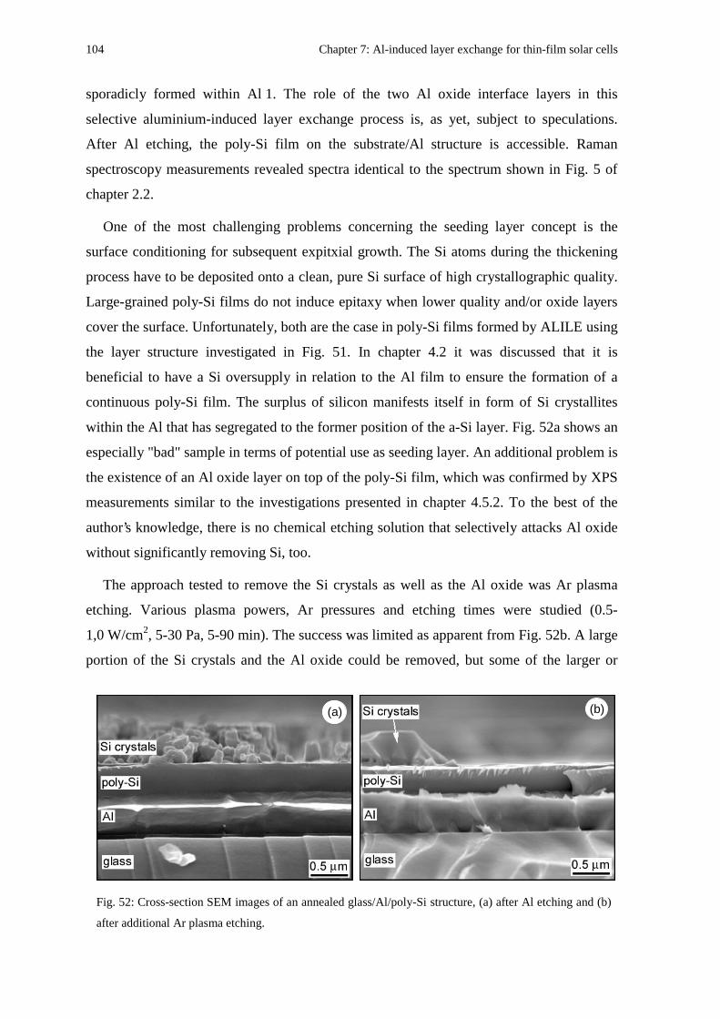
104 Chapter 7: Al-induced layer exchange for thin-film solar cells
sporadicly formed within Al 1. The role of the two Al oxide interface layers in this
selective aluminium-induced layer exchange process is, as yet, subject to speculations.
After Al etching, the poly-Si film on the substrate/Al structure is accessible. Raman
spectroscopy measurements revealed spectra identical to the spectrum shown in Fig. 5 of
chapter 2.2.
One of the most challenging problems concerning the seeding layer concept is the
surface conditioning for subsequent expitxial growth. The Si atoms during the thickening
process have to be deposited onto a clean, pure Si surface of high crystallographic quality.
Large-grained poly-Si films do not induce epitaxy when lower quality and/or oxide layers
cover the surface. Unfortunately, both are the case in poly-Si films formed by ALILE using
the layer structure investigated in Fig. 51. In chapter 4.2 it was discussed that it is
beneficial to have a Si oversupply in relation to the Al film to ensure the formation of a
continuous poly-Si film. The surplus of silicon manifests itself in form of Si crystallites
within the Al that has segregated to the former position of the a-Si layer. Fig. 52a shows an
especially "bad" sample in terms of potential use as seeding layer. An additional problem is
the existence of an Al oxide layer on top of the poly-Si film, which was confirmed by XPS
measurements similar to the investigations presented in chapter 4.5.2. To the best of the
author’s knowledge, there is no chemical etching solution that selectively attacks Al oxide
without significantly removing Si, too.
The approach tested to remove the Si crystals as well as the Al oxide was Ar plasma
etching. Various plasma powers, Ar pressures and etching times were studied (0.5-
1,0 W/cm2, 5-30 Pa, 5-90 min). The success was limited as apparent from Fig. 52b. A large
portion of the Si crystals and the Al oxide could be removed, but some of the larger or
(a) (b)
Fig. 52: Cross-section SEM images of an annealed glass/Al/poly-Si structure, (a) after Al etching and (b)
after additional Ar plasma etching.
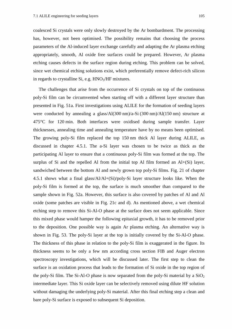
7.1 ALILE engineering for seeding layers 105
coalesced Si crystals were only slowly destroyed by the Ar bombardment. The processing
has, however, not been optimised. The possibility remains that choosing the process
parameters of the Al-induced layer exchange carefully and adapting the Ar plasma etching
appropriately, smooth, Al oxide free surfaces could be prepared. However, Ar plasma
etching causes defects in the surface region during etching. This problem can be solved,
since wet chemical etching solutions exist, which preferentially remove defect-rich silicon
in regards to crystalline Si, e.g. HNO3/HF mixtures.
The challenges that arise from the occurrence of Si crystals on top of the continuous
poly-Si film can be circumvented when starting off with a different layer structure than
presented in Fig. 51a. First investigations using ALILE for the formation of seeding layers
were conducted by annealing a glass/Al(300 nm)/a-Si (300 nm)/Al(150 nm) structure at
475°C for 120 min. Both interfaces were oxidised during sample transfer. Layer
thicknesses, annealing time and annealing temperature have by no means been optimised.
The growing poly-Si film replaced the top 150 nm thick Al layer during ALILE, as
discussed in chapter 4.5.1. The a-Si layer was chosen to be twice as thick as the
participating Al layer to ensure that a continuous poly-Si film was formed at the top. The
surplus of Si and the repelled Al from the initial top Al film formed an Al+(Si) layer,
sandwiched between the bottom Al and newly grown top poly-Si films. Fig. 21 of chapter
4.5.1 shows what a final glass/Al/Al+(Si)/poly-Si layer structure looks like. When the
poly-Si film is formed at the top, the surface is much smoother than compared to the
sample shown in Fig. 52a. However, this surface is also covered by patches of Al and Al
oxide (some patches are visible in Fig. 21c and d). As mentioned above, a wet chemical
etching step to remove this Si-Al-O phase at the surface does not seem applicable. Since
this mixed phase would hamper the following epitaxial growth, it has to be removed prior
to the deposition. One possible way is again Ar plasma etching. An alternative way is
shown in Fig. 53. The poly-Si layer at the top is initially covered by the Si-Al-O phase.
The thickness of this phase in relation to the poly-Si film is exaggerated in the figure. Its
thickness seems to be only a few nm according cross section FIB and Auger electron
spectroscopy investigations, which will be discussed later. The first step to clean the
surface is an oxidation process that leads to the formation of Si oxide in the top region of
the poly-Si film. The Si-Al-O phase is now separated from the poly-Si material by a SiO2
intermediate layer. This Si oxide layer can be selectively removed using dilute HF solution
without damaging the underlying poly-Si material. After this final etching step a clean and
bare poly-Si surface is exposed to subsequent Si deposition.
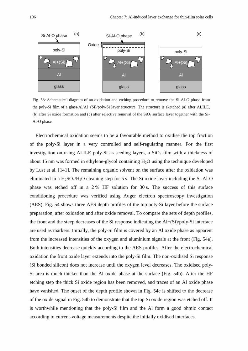
106 Chapter 7: Al-induced layer exchange for thin-film solar cells
Electrochemical oxidation seems to be a favourable method to oxidise the top fraction
of the poly-Si layer in a very controlled and self-regulating manner. For the first
investigation on using ALILE poly-Si as seeding layers, a SiO2 film with a thickness of
about 15 nm was formed in ethylene-glycol containing H2O using the technique developed
by Lust et al. [141]. The remaining organic solvent on the surface after the oxidation was
eliminated in a H2SO4/H2O cleaning step for 5 s. The Si oxide layer including the Si-Al-O
phase was etched off in a 2 % HF solution for 30 s. The success of this surface
conditioning procedure was verified using Auger electron spectroscopy investigation
(AES). Fig. 54 shows three AES depth profiles of the top poly-Si layer before the surface
preparation, after oxidation and after oxide removal. To compare the sets of depth profiles,
the front and the steep decreases of the Si response indicating the Al+(Si)/poly-Si interface
are used as markers. Initially, the poly-Si film is covered by an Al oxide phase as apparent
from the increased intensities of the oxygen and aluminium signals at the front (Fig. 54a).
Both intensities decrease quickly according to the AES profiles. After the electrochemical
oxidation the front oxide layer extends into the poly-Si film. The non-oxidised Si response
(Si bonded silicon) does not increase until the oxygen level decreases. The oxidised poly-
Si area is much thicker than the Al oxide phase at the surface (Fig. 54b). After the HF
etching step the thick Si oxide region has been removed, and traces of an Al oxide phase
have vanished. The onset of the depth profile shown in Fig. 54c is shifted to the decrease
of the oxide signal in Fig. 54b to demonstrate that the top Si oxide region was etched off. It
is worthwhile mentioning that the poly-Si film and the Al form a good ohmic contact
according to current-voltage measurements despite the initially oxidised interfaces.
glass
Al
Al+(Si)
poly-Si
Si-Al-O phase
glass
Al
Al+(Si)
poly-Si
Si-Al-O phase
Oxide
(a) (b)
glass
Al
Al+(Si)
poly-Si
(c)
Fig. 53: Schematical diagram of an oxidation and etching procedure to remove the Si-Al-O phase from
the poly-Si film of a glass/Al/Al+(Si)/poly-Si layer structure. The structure is sketched (a) after ALILE,
(b) after Si oxide formation and (c) after selective removal of the SiO2 surface layer together with the Si-
Al-O phase.
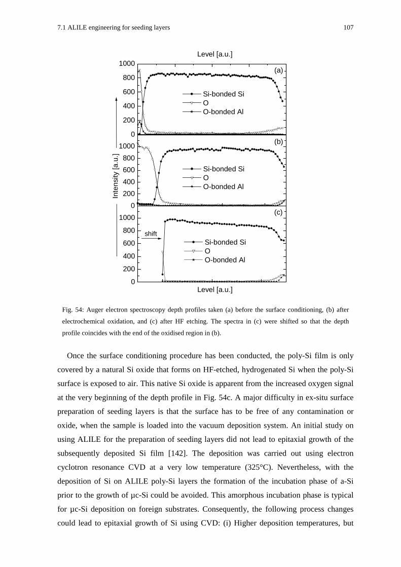
7.1 ALILE engineering for seeding layers 107
Once the surface conditioning procedure has been conducted, the poly-Si film is only
covered by a natural Si oxide that forms on HF-etched, hydrogenated Si when the poly-Si
surface is exposed to air. This native Si oxide is apparent from the increased oxygen signal
at the very beginning of the depth profile in Fig. 54c. A major difficulty in ex-situ surface
preparation of seeding layers is that the surface has to be free of any contamination or
oxide, when the sample is loaded into the vacuum deposition system. An initial study on
using ALILE for the preparation of seeding layers did not lead to epitaxial growth of the
subsequently deposited Si film [142]. The deposition was carried out using electron
cyclotron resonance CVD at a very low temperature (325°C). Nevertheless, with the
deposition of Si on ALILE poly-Si layers the formation of the incubation phase of a-Si
prior to the growth of µc-Si could be avoided. This amorphous incubation phase is typical
for µc-Si deposition on foreign substrates. Consequently, the following process changes
could lead to epitaxial growth of Si using CVD: (i) Higher deposition temperatures, but
0
200
400
600
800
1000
Si-bonded Si O O-bonded Al
(a)
Level [a.u.]
Inte
nsity
[a.u
.]
0
200
400
600
800
1000
Si-bonded Si O O-bonded Al
(c)
(b)
0
200
400
600
800
1000
Si-bonded Si O O-bonded Al
shift
Level [a.u.]
Fig. 54: Auger electron spectroscopy depth profiles taken (a) before the surface conditioning, (b) after
electrochemical oxidation, and (c) after HF etching. The spectra in (c) were shifted so that the depth
profile coincides with the end of the oxidised region in (b).
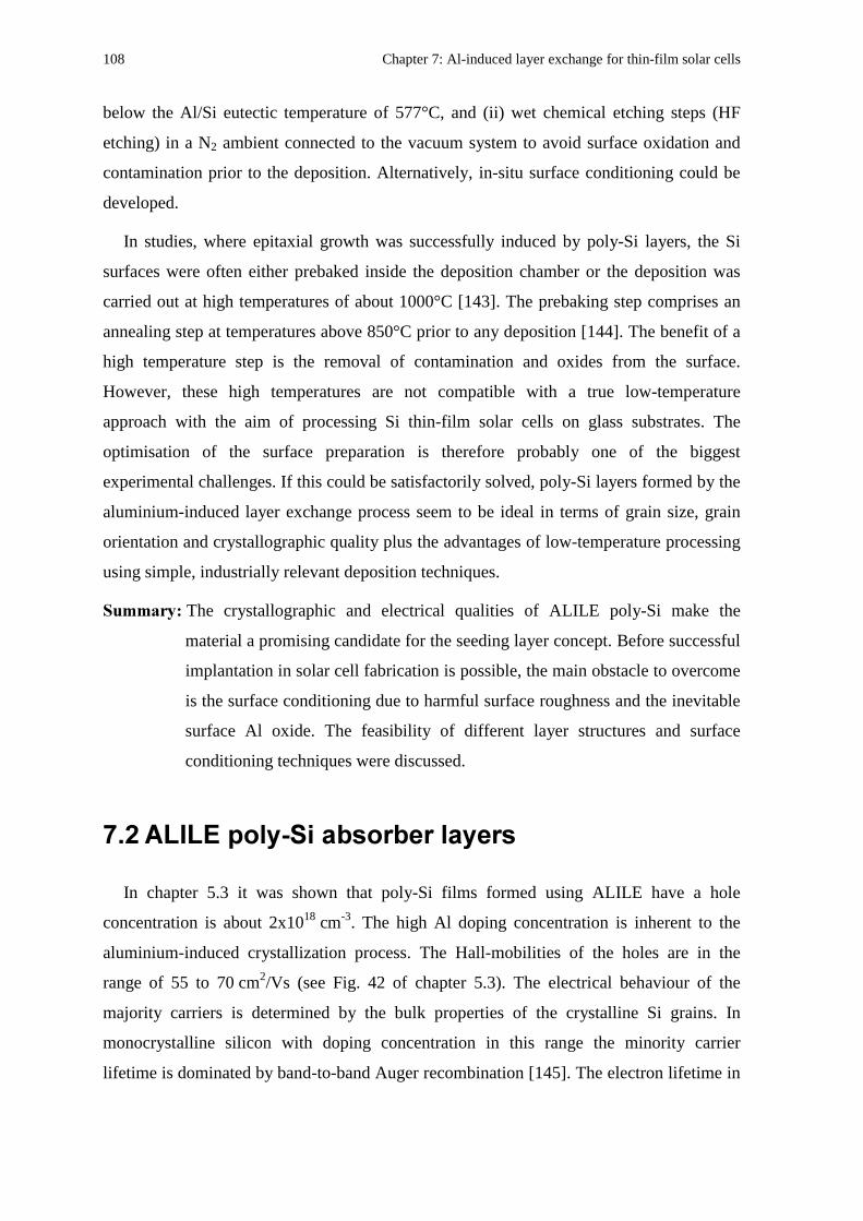
108 Chapter 7: Al-induced layer exchange for thin-film solar cells
below the Al/Si eutectic temperature of 577°C, and (ii) wet chemical etching steps (HF
etching) in a N2 ambient connected to the vacuum system to avoid surface oxidation and
contamination prior to the deposition. Alternatively, in-situ surface conditioning could be
developed.
In studies, where epitaxial growth was successfully induced by poly-Si layers, the Si
surfaces were often either prebaked inside the deposition chamber or the deposition was
carried out at high temperatures of about 1000°C [143]. The prebaking step comprises an
annealing step at temperatures above 850°C prior to any deposition [144]. The benefit of a
high temperature step is the removal of contamination and oxides from the surface.
However, these high temperatures are not compatible with a true low-temperature
approach with the aim of processing Si thin-film solar cells on glass substrates. The
optimisation of the surface preparation is therefore probably one of the biggest
experimental challenges. If this could be satisfactorily solved, poly-Si layers formed by the
aluminium-induced layer exchange process seem to be ideal in terms of grain size, grain
orientation and crystallographic quality plus the advantages of low-temperature processing
using simple, industrially relevant deposition techniques.
' The crystallographic and electrical qualities of ALILE poly-Si make the
material a promising candidate for the seeding layer concept. Before successful
implantation in solar cell fabrication is possible, the main obstacle to overcome
is the surface conditioning due to harmful surface roughness and the inevitable
surface Al oxide. The feasibility of different layer structures and surface
conditioning techniques were discussed.
6%77' 33
In chapter 5.3 it was shown that poly-Si films formed using ALILE have a hole
concentration is about 2x1018 cm-3. The high Al doping concentration is inherent to the
aluminium-induced crystallization process. The Hall-mobilities of the holes are in the
range of 55 to 70 cm2/Vs (see Fig. 42 of chapter 5.3). The electrical behaviour of the
majority carriers is determined by the bulk properties of the crystalline Si grains. In
monocrystalline silicon with doping concentration in this range the minority carrier
lifetime is dominated by band-to-band Auger recombination [145]. The electron lifetime in
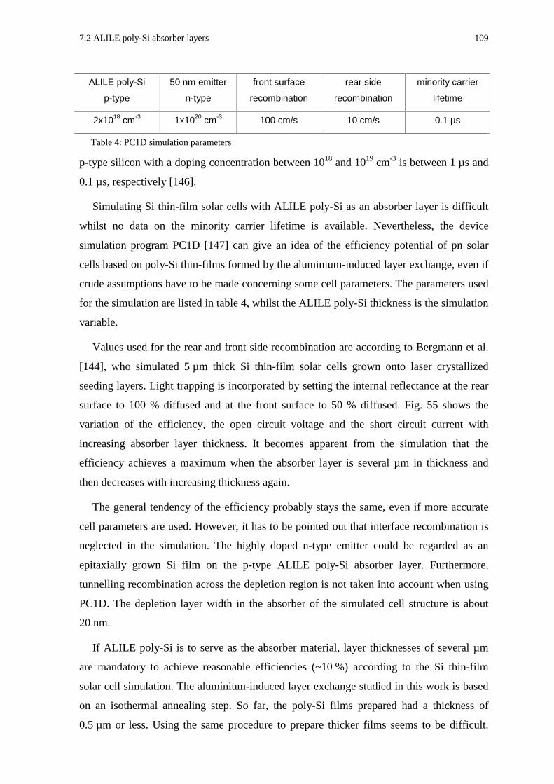
7.2 ALILE poly-Si absorber layers 109
p-type silicon with a doping concentration between 1018 and 1019 cm-3 is between 1 µs and
0.1 µs, respectively [146].
Simulating Si thin-film solar cells with ALILE poly-Si as an absorber layer is difficult
whilst no data on the minority carrier lifetime is available. Nevertheless, the device
simulation program PC1D [147] can give an idea of the efficiency potential of pn solar
cells based on poly-Si thin-films formed by the aluminium-induced layer exchange, even if
crude assumptions have to be made concerning some cell parameters. The parameters used
for the simulation are listed in table 4, whilst the ALILE poly-Si thickness is the simulation
variable.
Values used for the rear and front side recombination are according to Bergmann et al.
[144], who simulated 5 µm thick Si thin-film solar cells grown onto laser crystallized
seeding layers. Light trapping is incorporated by setting the internal reflectance at the rear
surface to 100 % diffused and at the front surface to 50 % diffused. Fig. 55 shows the
variation of the efficiency, the open circuit voltage and the short circuit current with
increasing absorber layer thickness. It becomes apparent from the simulation that the
efficiency achieves a maximum when the absorber layer is several µm in thickness and
then decreases with increasing thickness again.
The general tendency of the efficiency probably stays the same, even if more accurate
cell parameters are used. However, it has to be pointed out that interface recombination is
neglected in the simulation. The highly doped n-type emitter could be regarded as an
epitaxially grown Si film on the p-type ALILE poly-Si absorber layer. Furthermore,
tunnelling recombination across the depletion region is not taken into account when using
PC1D. The depletion layer width in the absorber of the simulated cell structure is about
20 nm.
If ALILE poly-Si is to serve as the absorber material, layer thicknesses of several µm
are mandatory to achieve reasonable efficiencies (~10 %) according to the Si thin-film
solar cell simulation. The aluminium-induced layer exchange studied in this work is based
on an isothermal annealing step. So far, the poly-Si films prepared had a thickness of
0.5 µm or less. Using the same procedure to prepare thicker films seems to be difficult.
ALILE poly-Si
p-type
50 nm emitter
n-type
front surface
recombination
rear side
recombination
minority carrier
lifetime
2x1018 cm-3 1x1020 cm-3 100 cm/s 10 cm/s 0.1 µs
Table 4: PC1D simulation parameters
110 Chapter 7: Al-induced layer exchange for thin-film solar cells
The reason is rooted in the existence of inter- and intra-grain Al clusters as discussed in
chapter 5.1. These Al clusters occur when the Si grains have impinged and form a
continuous layer along the Al/a-Si interface before all Al has been repelled from its
original position. Consequently, some Al can still be found near the substrate.
Fig. 56 reveals the problem when thicker Al/a-Si layer structures are isothermally
annealed. The structure depicted initially consisted of a glass substrate with 4 µm Al and
4 µm a-Si deposited. Although a poly-Si film has formed, it did not replace the thick Al
layer entirely. A large fraction of the Al remains at the substrate. The continuous poly-Si
film along the interface blocks the diffusion of the Si atoms from the amorphous phase into
the Al film and therefore further Si crystallization. The layer exchange process terminates
at this stage. Even extended annealing (>50 h) does not seem to have any effect on this
final state. The top layer is a mixture of segregated Al and partially crystallized Si
according to Raman spectroscopy. Throughout chapter 4, a whole set of process
parameters of ALILE was discussed. There might be a possibility of choosing these
parameters appropriately, so an entire layer exchange can be achieved even with layers of a
couple of µm in thickness. The general direction for choosing the parameters would be to
0 2 4 6 8 108
9
10
11
12
13
14
15
Effi
cien
cy [%
]
ALILE poly-Si thickness [µm]
0 2 4 6 8 100.60
0.61
0.62
0.63
0.64
0.65
VO
C [v
]
ALILE poly-Si thickness [µm]
VOC
20
25
30
35
Isc [mA
/cm2]
Isc
(a)
(b)
Fig. 55: Si thin-film solar cell simulation using PC1D. The cell parameters are documented in table 4.
7.2 ALILE poly-Si absorber layers 111
aim for a low nucleation rate. The fewer grains form, the larger they can grow before
impingement occurs. The grain sizes ought to exceed the Al layer thickness many times
even if this thickness is several µm. The Al that induces the crystallization process has to
be repelled from its original position before a continuous poly-Si film forms.
Substituting the isothermal annealing step might be a possible way to form ALILE poly-
Si films with several µm in thickness. Temperature gradient and locally varying
temperature profile annealing processes are currently under investigation. The research
direction, which might lead to successful preparation of thick ALILE poly-Si films, is still
open. The a-Si/Al structures investigated in this work were chosen to enable the detailed
study of the aluminium-induced layer exchange process. The rudimentary process can be
extended in many directions; varying the layer structure, the annealing procedure, the
deposition parameters, even the crystallization inducing metal provides a wide range of
possibilities. It is likely that one of these paths will lead to the formation of poly-Si films
based on the metal-induced layer exchange process, which is feasible for Si thin-film solar
cell fabrication.
' Using ALILE poly-Si films as absorber material in Si thin-film solar cells is an
entirely new field. The main concern is the process inherent high doping
concentration. Due to the high crystallographic quality of the poly-Si films
there is a chance that the minority carrier lifetime is only limited by Auger
recombination and not by grain boundary or inner-grain defects. If this is the
case, it is likely that solar cell efficiencies of over 10 % could be achieved. The
most difficult obstacle that has to be overcome is to process poly-Si films of
several µm in thickness using ALILE. It seems that a significantly different
annealing concept than isothermal annealing will have to be applied. If the
Fig. 56: Cross section FIB micrograph of an annealed sample with an initial layer structure of 4 µm Al
and 4 µm a-Si. The sample was annealed at 425°C for 60 h.

112 Chapter 7: Al-induced layer exchange for thin-film solar cells
aluminium-induced layer exchange process can be extended in this direction
maintaining its simplicity, it will be a promising candidate to form large-
sssgrained polycrystalline silicon films on foreign-substrates at low
temperatures using industrially relevant techniques.
113
8
In this work, the aluminium-induced layer exchange process (ALILE) is investigated.
ALILE is based on aluminium-induced crystallization, which is the phenomenon of the
transformation of amorphous to crystalline silicon when in contact with Al at temperatures
well below the Al/Si eutectic temperature of 577°C. Throughout this study, it is shown for
the first time that aluminium-induced crystallization of a-Si can instigate a complete layer
exchange of adjacent a-Si and Al films on foreign substrates. During this exchange process
a continuous poly-Si film is formed.
ALILE is influenced by a list of process parameters: (i) The annealing time, (ii) the ratio
of the a-Si and Al layer thicknesses, (iii) the annealing temperature, (iv) the structure of the
polycrystalline Al, (v) the interface oxide layer and (vi) the layer sequence. In this work
the aluminium-induced layer exchange process as well as the material properties of the
poly-Si film on glass are studied. From these investigations the following results are
extracted:
• The a-Si is dissociated by the adjacent Al layer. The dissolved Si atoms crystallize
within the polycrystalline aluminium. The Si grain growth is vertically confined by the
substrate and the a-Si/Al interface. Laterally the grains can grow within the Al matrix
to sizes of several µm in diameter before impingement of neighbouring grains occurs.
The Al is repelled from the advancing crystallization front of the Si grains and occupies
the space of the former a-Si layer. The overall reaction is therefore the layer exchange.
• The annealing temperature influences the grain size of the poly-Si film in a way that
the lower the temperature, the larger the Si grains. However, the overall layer exchange
process is significantly slowed down at lower temperatures. Processing times needed
might then exceed one hour. It is also shown that the lower the temperature, the more
prevalent the dendritic Si growth within the Al matrix.
• Because the grain boundaries of the polycrystalline Al are preferential nucleation sites
for the Si solute, it is found that the higher the density of Al grain boundaries, the
114 Chapter 8: Conclusions
higher the Si nucleation rate, and the faster the exchange process, but the smaller the
grains of the continuous poly-Si film.
• The interface oxide between the Al and a-Si layers is a mandatory requirement for the
successful layer exchange. The interface consists of a stable Al oxide. If Si oxide
initially separates the two layers, the SiO2 is reduced to Al oxide. The oxide layer
remains between the two films, although practically all Al and Si atoms exchange sides
with respect to the interface. The oxide interface also enables the selective layer
exchange in a stacked layer system, e.g. a glass/Al/a-Si/Al structure transforms to
glass/Al/Al/poly-Si during ALILE.
• The continuous poly-Si films have an Al concentration of about 3x1019 cm-3. Besides
these Al atoms incorporated within the poly-Si film, the poly-Si/substrate system
additionally contains intra- and inter-grain Al clusters, which are sporadically trapped
between the glass and the Si film.
• The poly-Si films can consist of grains, whose lateral diameter exceed 10 µm. Some of
the larger grains exhibit a subgrain structure where coincident site lattice grain
boundaries with coincidence index Σ3 and Σ9 separate areas of different
crystallographic orientation. These twin boundaries develop during the growth of
individual Si grains. The grains have a preferential (100) orientation.
• A large share of the incorporated Al occupies substitutional Si lattice sites. The Al
atoms introduce acceptor levels in the Si band structure and give rise to a hole
concentration of about 2x1018 cm-3. The Hall mobility of the majority carriers is in the
range of 55-70 cm/Vs. The hole concentration as well as the hole mobility vary little
with annealing temperature.
The attempt is made to give a comprehensive model of the aluminium-induced layer
exchange, although little is still known about some of the sub-steps of the process. It is
suggested that the driving force for the dissociation of a-Si and yet the formation of c-Si is
the chemical potential difference of Si atoms at the a-Si/Al and the Al/c-Si interfaces. The
description of the formation process of large-grained poly-Si during ALILE is based on the
model of interfering Si grains at an early stage of the crystallization process. It is proposed
that existing grains deplete the adjacent Al matrix. The Si depletion regions therefore
extend from the advancing Si crystallization front into the Al solvent. When the Si
depletion regions of neighbouring grains begin to overlap, the formation of new Si nuclei
is suppressed. Since the grain density is kept low because of this interference mechanism,
Chapter 8: Conclusions 115
the individual grains can grow to large sizes before a continuous poly-film is formed. It is
pointed out that the main open question is the particular role of the interface oxide.
Different types of investigations are suggested to elucidate in more detail this interface
oxide layer.
The aluminium-induced layer exchange process investigated in this work fits well
within the low-temperature approach to fabricate poly-Si thin-film solar cells. The main
advantages of the layer exchange process are: (i) Low processing temperature (<550°C),
(ii) cost-efficient substrates (glass), (iii) industrially relevant deposition techniques
(thermal evaporation and sputtering deposition), (iii) relatively short crystallization time
(~30 min) and (iv) simple. For the time being, ALILE is the only true low-temperature
process that can combine all these characteristics. Especially in comparison with solid
phase and laser crystallization, the aluminium-induced layer exchange process seems to be
a very promising candidate for processing of large-grained poly-Si films on foreign
substrates within the framework of the low-temperature approach. The main obstacles that
seem to hamper the successful use of poly-Si films formed using ALILE are (a) the high
doping concentration and (b) the difficulty in processing films with several µm in
thickness. The high doping concentration is an inherent characteristic of the aluminium-
induced crystallization process, which might restrict the application of these films to the
use as seeding layers for subsequent epitaxial growth. The difficulty of forming several µm
thick poly-Si layers might be overcome by substituting the isothermal annealing process
used in this work with more sophisticated annealing procedures.
The study on metal-induced crystallization of amorphous silicon presented in this work
focused on the aluminium-induced layer exchange. Due to the success in forming large-
grained poly-Si in a simple way at low temperatures, it is an exciting field for further
investigations. The work discussed here is only the tip of the iceberg for the fabrication of
large-grained poly-Si thin-films based on a metal-induced layer exchange process.
Different metals, that induce the Si crystallization, varying layer structures and modified
annealing procedures are imaginable and could lead to a new way of processing poly-Si
films on foreign, low-cost substrates for Si thin-film device applications.
Al

117
$
[1] K. Zweig and M. A. Green, Progr. Photovolt. *, 1 (2000).
[2] S. H. Kim, C. MacCracken, and J. Edmonds, Progr. Photovolt. *, 3 (2000).
[3] G. Giroult-Matlakowski, “Photovoltaic Market Analysis,” presented at the
, (Vienna, 1998),
p.3403.
[4] A. Shah, P. Torres, R. Tscharner, N. Wyrsch, and H. Keppner, Science *, 692
(1999).
[5] Z. Shi and M. A. Green, Progr. Photovolt. (, 247 (1998).
[6] W. Fuhs and R. Klenk, “Thin-Film Solar Cells-Overview,” presented at the
, (Vienna, 1998),
p.381.
[7] A. V. Shah, R. Platz, and H. Keppner, Sol. En. Mat. and Sol. Cells *, 501 (1995).
[8] V. M. Fthenakis and P. D. Moskowitz, Progr. Photovolt. *, 27 (2000).
[9] B. A. Andersson, Progr. Photovolt. *, 61 (2000).
[10] O.-A. Neumüller, ! "#$, 7 ed. (Franckh'sche Verlangshandlung,
Stuttgart, 1975).
[11] J. H. Werner, R. Bergmann, and R. Brendel, “The Challenge of Crystalline Thin Film
Silicon Solar Cells,” in %$ & , edited
by R. Helbig (Vieweg, Braunschweig, 1995), Vol. 34, p. 115.
[12] R. Brendel, R. B. Bergmann, P. Lolgen, M. Wolf, and J. H. Werner, Appl. Phys. Lett.
), 390 (1997).
[13] D. Thorp, P. Campbell, and S. R. Wenham, Progr. Photovolt. #, 205 (1996).
[14] K. Yamamoto, M. Yoshimi, Y. Tawada, Y. Okamoto, A. Nakajima, and S. Igari,
Appl. Phys. A (&, 179 (1999).
[15] R. B. Bergmann, Appl. Phys. A (&, 187 (1999).
[16] R. E. I. Schropp and M. Zeman, ' ( (
' )' *+ (Kluwer Acadamic, Boston, 1998).
[17] S. Reber and W. Wettling, Appl. Phys. A (&, 215 (1999).
[18] R. B. Bergmann, G. Oswald, M. Albrecht, and V. Gross, Sol. En. Mat. and Sol. Cells
#(, 147 (1997).
118 References
[19] C. Spinella, S. Lombardo, and F. Priolo, J. Appl. Phys. *#, 5383 (1998).
[20] K. Ishikawa, M. Ozawa, C.-H. Oh, and M. Matsumura, Jpn. J. Appl. Phys. , 731
(1998).
[21] R. S. Sposili and J. S. Im, Appl. Phys. Lett. (&, 2864 (1996).
[22] J. S. Im, H. J. Kim, and M. O. Thompson, Appl. Phys. Lett. ( , 1969 (1993).
[23] G. Andrä, J. Bergmann, F. Falk, and E. Ose, “Laser induced liquid phase
crystallization of amorphous silicon films on glass for thin film solar cells,” presented
at the ,- ( , (Barcelona, 1997),
p.1400.
[24] S. R. Herd, P. Chaudhari, and M. H. Brodsky, J. Non-Crystall. Solids , 309 (1972).
[25] T.-K. Kim, T.-H. Ihn, B.-I. Lee, and S.-K. Joo, Jpn. J. Appl. Phys. , 4244 (1998).
[26] J. Jang, J. Y. Oh, S. K. Kim, Y. j. Choi, S. Y. Yoon, and C. O. Kim, Nature &, 481
(1998).
[27] L. K. Lam, S. K. Chen, and D. G. Ast, Appl. Phys. Lett. #, 1866 (1999).
[28] M. Boreland, K. Yamaguchi, K. Okitsu, M. Imaizumi, and M. Yamaguchi, “One Step
Aluminium Induced Crystal Growth of nc-Si Thin Films Using Electron Beam Excited
Plasma Chemical Vapour Deposition,” presented at the ,.
( , (Glasgow, 2000).
[29] S. Summers, L. Wang, H. S. Reehal, and G. J. Hirst, “Excimer laser and aluminium-
induced crystallisation of silicon thin films on foreign substrates for solar cells,”
presented at the ,. ( ,
(Glasgow, 2000).
[30] K. Shirasawa, H. Senta, H. Hakuma, M. Komoda, K. Fukui, and K. Niira, “Thin film
poly-Si formation for solar cells by flux method, CAT-CVD method & PECVD
Method,” presented at the ,. (
, (Glasgow, 2000).
[31] R. Bergmann, J. Kühnle, and J. H. Werner, “Polycrystalline silicon for thin film solar
cells,” presented at the , ,
(Hawai, 1994), p.1398.
[32] Z. Shi, T. L. Young, and M. A. Green, “Solution growth of polycrystalline silicon on
glass at low temperatures,” presented at the ,
, (Hawaii, 1994), p.1579.
[33] T. Matsuyama, T. Baba, T. Tsuyoshi, S. Tsuda, and S. Nakano, Sol. En. Mat. and Sol.
Cells #, 285 (1994).
References 119
[34] J.-S. Maa and S.-J. Lin, Thin-Solid-Films (#, 63 (1979).
[35] B. Bian, J. Yie, B. Li, and Z. Wu, J. Appl. Phys. , 7402 (1993).
[36] L. Hultman, A. Robertsson, H. T. G. Hentzell, I. Engström, and P. A. Psaras, J. Appl.
Phys. (, 3647 (1987).
[37] S. F. Gong, H. T. G. Hentzell, A. E. Robertsson, L. Hultman, S. E. Hörnström, and G.
Radnoczi, J. Appl. Phys. (, 3726 (1987).
[38] S. W. Russell, L. Jian, and J. W. Mayer, J. Appl. Phys. ), 5153 (1991).
[39] S. Y. Yoon, K. Ki Hyung, K. Chae Ok, O. Jae Young, and J. Jin, J. Appl. Phys. *,
5865 (1997).
[40] T. B. Massalski, / *, 2nd ed. (ASM International, Materials
Park, Ohio, 1990).
[41] M. S. Ashtikar and G. L. Sharma, J. Appl. Phys. *, 913 (1995).
[42] C. Hayzelden and J. L. Batstone, J. Appl. Phys. , 8279 (1993).
[43] Z. Jin, G. A. Bhat, M. Yeung, H. S. Kwok, and M. Wong, J. Appl. Phys. *#, 194
(1998).
[44] J. L. Batstone and C. Hayzelden, Solid State Phenomena *, 257 (1994).
[45] C. C. Tsai, R. J. Nemanich, and M. J. Thompson, J. Vac. Sci. Technol. , 632 (1982).
[46] T. J. Konno and R. Sinclair, Mater. Sci. Engin. %&1%*), 426 (1994).
[47] T. J. Konno and R. Sinclair, Philosophical Magazine B ((, 749 (1992).
[48] L. H. Allen, J. R. Phillips, D. Theodore, C. B. Carter, R. Soave, J. W. Mayer, and G.
Ottaviani, Phys. Rev. B #, 8203 (1990).
[49] L. H. Allen, J. W. Mayer, K. N. Tu, and L. C. Feldman, Phys. Rev. B #, 8213 (1990).
[50] J. M. Harris, R. J. Blattner, I. D. Ward, C. A. Evans, H. L. Fraser, M. A. Nicolet, and
C. L. Ramiller, J. Appl. Phys. #*, 2897 (1977).
[51] K. Nakamura, M.-A. Nicolet, J. W. Mayer, R. J. Blattner, and C. A. Evans, Jr, Appl.
Phys. Lett. #(, 4678 (1975).
[52] G. Majni and G. Ottaviani, Appl. Phys. Lett. , 125 (1977).
[53] B. Y. Tsaur, G. W. Turner, and J. C. C. Fan, Appl. Phys. Lett. &, 749 (1981).
[54] L. M. Koschier, S. R. Wenham, M. Gross, T. Puzzer, and A. B. Sproul, “Low
temperature junction and back surface field formation for photovoltaic devices,”
presented at the
, (Vienna, 1998), p.1539.
[55] S. R. Wenham, L. M. Koschier, O. Nast, and C. B. Honsberg, IEEE Transactions on
Electron Devices #(, 2005 (1999).
120 References
[56] F. A. Trumbore, Bell Syst. Tech. J. &, 205 (1960).
[57] S. M. Sze, (*, 2 ed. (Wiley & Sons, New York, 1981).
[58] T. P. Drüsedau, J.Bläsing, and H. Gnaser, Appl. Phys. Lett. , 1510 (1998).
[59] T. P. Drüsedau, A. Diez, and J. Blasing, Thin Solid Films , 41 (1999).
[60] S. A. Lyon, R. J. Nemanich, N. M. Johnson, and N. M. Biegelsen, Appl. Phys. Lett.
#), 316 (1982).
[61] H. Richter, Z.P.Wang, and L. Ley, Solid State Communication &, 625 (1981).
[62] P. M. Fauchet and I. H. Campbell, Mat. Res. Soc. Symp. Proc. (#, 259 (1990).
[63] W. Kern, J. Electrochem. Soc. , 1887 (1990).
[64] T. K. Olson, R. G. Lee, and J. C. Morgan, “Contrast Mechanisms in Focused Ion
Beam Imaging,” presented at the ,01 (+2%
, (Los Angeles, California, 1992), p.373.
[65] B. L. Adams, S. I. Wright, and K. Kunze, Metallurgical Transactions A #%, 819
(1993).
[66] J. I. Goldstein and H. Yakowitz, ( ' (Plenum
Press, New York, 1975).
[67] M. Schuster and H. Göbel, Adv. X-Ray Anal. &, 1 (1996).
[68] D. A. Porter and K. E. Easterling, +' , 2nd
ed. (Chapman&Hall, London, 1992).
[69] E. B. Graper, J. Vac. Sci. Technol. &, 33 (1971).
[70] P. G. Shewmon, “Diffusion,” in ' , edited by R.W. Cahn (North-
Holand Publishing Company, Amsterdam, 1970), p. 383.
[71] S. A. Flodstrom, R. Z. Bachrach, R. S. Bauer, and S. B. M. Hagström, Phys. Rev.
Lett. , 1282 (1976).
[72] J. L. Vossen and J. J. Cuomo, in +% , edited by J.L. Vossen and W.
Kern (Academic, New York, 1987).
[73] F. J. Grunthaner, P. J. Grunthaner, R. P. Vasques, B. F. Lewis, and J. Maserjian, Phys.
Rev. Lett. # , 1683 (1979).
[74] R. D. Thompson and K. N. Tu, Appl. Phys. Lett. #, 440 (1982).
[75] H. Nagel, A. G. Aberle, and S. Narayanan, Solid State Phenomena ((*, 503 (1999).
[76] J. A. Venables and C. J. Harland, Philos. Mag. , 1193 (1979).
[77] D. G. Brandon, Acta Metallurgica #, 1479 (1966).
[78] A. V. Nikoaleva and Y. A. Nikoalev, Materials-Science-Forum ))&, 657 (1996).
References 121
[79] A. Fedotov, B. Evtodyi, L. Fionova, Y. Ilyashuk, E. Katz, and L. Polyak, Physica-
Status-Solidi-A &, 523 (1990).
[80] A. Fedotov, B. Evtody, L. Fionova, J. Iliashuk, E. Katz, and L. Poljak, J. Cryst.
Growth )#, 186 (1990).
[81] M. Birkholz, S. Fiechter, A. Hartmann, and H. Tributsch, Phys. Rev. B # , 11926
(1991).
[82] National Bureau of Standards, NBS Standard Reference Material No. 640. Report No.
Vol. 13, 1976.
[83] L. Haji, P. Joubert, J. Stoemenos, and N. A. Economou, J. Appl. Phys. , 3944
(1994).
[84] S. Loreti, M. Vittori, L. Mariucci, and G. Fortunato, Solid State Phenomena ((*,
181 (1999).
[85] J. Platen, B. Selle, I. Sieber, U. Zimmer, and W. Fuhs, Mat. Res. Soc. Symp. Proc.
), 91 (1999).
[86] T. Noma, T. Yonehara, and H. Kumomi, Appl. Phys. Lett. &, 653 (1991).
[87] S. Selberherr, ( (* (Springer, Vienna,
1984).
[88] Landolt-Börnstein, “Numerical Data and Functional Relationships in Science and
Technology”, edited by M. Schulz (Springer, Berlin, 1989), Vol. III/22b.
[89] W. R. Thurber, R. L. Mattis, and Y. M. Liu, J. Electrochem. Soc. , 1807 (1980).
[90] C. S. Hung and J. R. Gliessman, Phys. Rev. &(, 1226 (1954).
[91] R. N. Bhatt and T. M. Rice, Phys. Rev. B , 1920 (1981).
[92] H. Ibach and H. Lüth, %$!$, 4 ed. (Springer-Verlag, Berlin, 1995).
[93] J. Y. W. Seto, J. Appl. Phys. #(, 5247 (1975).
[94] R. Enderlein and N. J. M. Horing, %
(World Scientific, Singapore, 1997).
[95] M. A. Green, J. Appl. Phys. (, 2944 (1990).
[96] J. S. Blakemore, ( (, Dover edition (General Publishing
Company, Toronto, 1987).
[97] R. A. Gudmundsen and J. Maserjian, J. Appl. Phys. *, 1308 (1957).
[98] J. H. Kim and J. Y. Lee, Jpn. J. Appl. Phys. , 2052 (1996).
[99] M. S. Haque, H. A. Naseem, and W. D. Brown, J. Appl. Phys. , 3928 (1994).
[100] T. Ito and Y. Nakayama, Transactions of the Japanese Institute of Metals , 375
(1984).
122 References
[101] U. Köster, phys. stat. sol. (a) #*, 313 (1978).
[102] J. O. McCaldin and H. Sankur, Appl. Phys. Lett. &, 524 (1971).
[103] R. A. Scranton and J. O. McCaldin, J. Vac. Sci. Technol. , 1358 (1978).
[104] J. O. McCaldin, J. Vac. Sci. Technol. , 990 (1974).
[105] C. Anandan, Appl. Surf. Sci. *&, 57 (1995).
[106] R. S. Bauer and R. Z. Bachrach, Appl. Phys. Lett. , 1006 (1980).
[107] R. Z. Bachrach and R. S. Bauer, J. Vac. Sci. Technol. (, 1149 (1979).
[108] J. A. Dean, #34 $, 13 ed. (McGraw-Hill Book Company,
New York, 1985).
[109] A. Bierhals, A. G. Aberle, and R. Hezel, J. Appl. Phys. * , 1371 (1998).
[110] K.-N. Tu, J. W. Mayer, and L. C. Feldman, +% ( (Macmillan
Publishing Company, New York, 1992).
[111] G. Ottaviani and G. Majni, J. Appl. Phys. ), 6865 (1979).
[112] H. Qingheng, E. S. Yang, and H. Izmirliyan, Solid-State Electronics , 1187 (1982).
[113] K. N. Tu, Appl. Phys. Lett. , 221 (1975).
[114] A. Hiraki, J. Electrochem. Soc. , 2662 (1980).
[115] M. S. Haque, H. A. Naseem, and W. D. Brown, J. Appl. Phys. &, 7529 (1996).
[116] A. Hiraki, Surf. Sci. (*, 74 (1986).
[117] P. W. Anderson, “Many-body effects at surfaces,” in
( )' , edited by J.A. Devreese, A.B. Kunz, and T.C.
Collins (Plenum Press, 1974), p. 1.
[118] J. C. Inkson, Surf. Sci. *, 69 (1971).
[119] A. Okiji, H. Kasai, and S. Terakawa, J. Phys. Soc. Jap. ##, 1275 (1978).
[120] G. Margaritondo, J. E. Rowe, and S. B. Christman, Phys. Rev. B #, 5396 (1976).
[121] G. Radnoczi, A. Robertsson, H. T. G. Hentzell, S. F. Gong, and M. A. Hasan, J.
Appl. Phys. (&, 6394 (1991).
[122] R. M. Walser and Bené, Appl. Phys. Lett. *, 624 (1976).
[123] R. W. Bené, J. Appl. Phys. (, 1862 (1987).
[124] A. E. Robertson, L. G. Hultman, H. T. G. Hentzell, S.-E. Hornstrom, and G.
Shaofang, J. Vac. Sci. Technol. A , 1447 (1987).
[125] H. T. G. Hentzell, A. Robertsson, L. Hultman, G. Shaofang, S. E. Hörnström, and P.
A. Psaras, Appl. Phys. Lett. ), 933 (1987).
[126] A. D. Pelton, “Thermodynamics and Phase Diagrams of Materials,” in
+' , edited by P. Haasen (VCH, Weinheim, 1991), Vol. 5.
References 123
[127] E. P. Donovan, F. Spaepen, D. Turnbull, J. M. Poate, and D. C. Jacobson, Appl.
Phys. Lett. #, 698 (1983).
[128] F. Spaepen, Philos. Mag. ) (1974).
[129] P. W. Atkins, (Oxford University Press, Oxford, 1998).
[130] G. J. van Gurp, J. Appl. Phys. ##, 2040 (1973).
[131] J. W. Christian, + + + ' , 1st ed.
(Pergamon Press, Oxford, 1965).
[132] C. Zener, J. Appl. Phys. ), 950 (1949).
[133] G. E. Murch, “Diffusion in Crystalline Solids,” in +
' , edited by Peter Haasen (VCH, Weinheim, 1991), Vol. 5, p. 75.
[134] T. J. Magee and J. Peng, J. Appl. Phys. #&, 4284 (1978).
[135] T. Kunze, S. Hauttmann, J. Seekamp, and J. Müller, “Recrystallized and epitaxially
thickened poly-Si lahers on graphite substrates,” presented at the . 1
( , (Anaheim, CA, 1997).
[136] R. B. Bergmann, C. Zaczek, N. Jansen, S. Oelting, and J. H. Werner, Appl. Phys.
Lett. , 2996 (1998).
[137] S. Reber, G. Stollwerck, D. Osswald, T. Kieliba, and C. Häßler, “Crystalline
silicicon thin-film solar cells on silicon nitride ceramcis,” presented at the ,.
( , (Glasgow, 2000).
[138] K. Yamamoto, A. Nakashima, T. Suzuki, and M. Yoshimi, Jpn. J. Appl. Phys. ,
L1751 (1994).
[139] A. Nakajima, T. Suzuki, M. Yoshimi, and K. Yamamoto, “Low temperature
fabrication and properties of the thin film polycrystalline Si solar cell on the glass
substrate,” presented at the ,56 ( 7, (Nice, 1995),
p.1550.
[140] K. Yamamoto, M. Yoshimi, T. Suzuki, Y. Okamoto, Y. Tawada, and A. Nakajima,
“Thin film poly-Si solar cell with "STAR Structure" on glass substrate fabricated at
low temperature,” presented at the . 1 ( ,
(Anaheim, 1997), p.575.
[141] S. Lust, J. Rappich, I. Sieber, W. Henrion, and W. Fuhs, presented at the ,.
( , (Glasgow, 2000).
[142] M. Birkholz, O. Nast, K. Kliefoth, E. Conrad, J. Rappich, P. Reinig, and W. Fuhs,
“Microcrystalline silicon grown on large-grained polycrystalline silicon formed by
124 References
aluminium-induced crystallisation,” presented at the ,.
( , (Glasgow, UK, 2000).
[143] R. Brendel, R. B. Bergmann, B. Fischer, J. Krinke, R. Plieninger, U. Rau, J. Reiß, H.
P. Strunk, H. Wanka, and J. H. Werner, “Transport Analysis for Polycrystalline
Silicon Solar Cells on Glass Substrates,” presented at the . 1
( , (Anaheim, CA, 1997), p.635.
[144] R. B. Bergmann, R. M. Hausner, N. Jensen, M. Grauvogl, L. Oberbeck, T. Rinke, M.
B. Schubert, C. Zaczek, R. Dassow, J. R. Köhler, U. Rau, S. K. Oelting, J. , H. P.
Strunk, and J. H. Werner, “High Rate, Low Temperature Deposition of Crystalline
Silicon Films for Thin Film Solar Cells on Glass,” presented at the
( , (Vienna, 1998),
p.1260.
[145] M. A. Green, ( ( 2 (Centre for
Photovoltaic Devices and Systems, University of New South Wales, Rosebbery,
1995).
[146] J. Dziewior and W. Schmid, Appl. Phys. Lett. , 346 (1977).
[147] D. A. Clugston and P. A. Basore, presented at the .1 (
, (Picataway, 1997), p.207.
125
% +*
I would like to thank Prof. W. Fuhs from the Hahn-Meitner-Insitut Berlin (HMI) for his
fantastic support of my research project from idea to finish. Many thanks also to Profs. M.
A. Green and S. R. Wenham, who made it possible for me to conduct the majority of my
work at the Photovoltaic Special Research Centre (PVSRC - now Centre for Photovoltaic
Engineering), University of New South Wales, Sydney. Without their support, this work
would not have been possible.
I would like to thank Prof. G. Weiser for accepting to be co-referee of this thesis.
Many thanks to ALL the members of the PVSRC for the wonderful, interesting time I
had there. My special thanks go to Drs. Tom Puzzer and Mark Gross for their brilliant help
in deposition and microscopy matters. Thanks heaps to Drs. Matt Boreland and Pietro
Altermatt. Furthermore, I’d like to thank Drs. Aihua Wang and Jianhua Zhao, as well as
Dr. Armin G. Aberle for his support after he became head of the thin-film group at the end
of 1998. And, of course, many thanks to the legendary legends of room 132, Dirk-Holger
Neuhaus, Keith McIntosh and Stephen Pritchard.
I would like to thank Dr. Cheng Tsien Chou from Pacific Solar, Sydney, for the
orientation imaging microscopy measurements, and Dr. Andreas J. Hartmann from the
Centre for Surface Science and Technology, University of New South Wales for the XPS
measurements.
I would like to thank ALL my colleagues from the HMI, in particular Drs. Stephan
Brehme, Mario Birkholz, Klaus Lips for measurements and discussions. Thanks to Dr. A.
Schöpke and Mr. Matthias Rebien for AES and ellipsometry measurements, respectively.
I’d also like to thank Dr. Jörg Rappich, Ms. G. Keiler, Ms. M. Schmidt, Mr. Peter Reinig
and Mr. René Linke for their support in sample preparation during my time at the HMI.
I acknowledge the financial support from the German Academic Exchange Service
under the HSPIII program.
AND, I am indebted to each one of the Coogee Gang for a fabulous time down under
and above all to Nicola Hartley.

127
Some of the results presented in this work have been published in scientific journals and
presented at conferences. The publications are as follows:
• O. Nast and A. J. Hartmann, "Influence of interface and Al structure on layer exchange
during aluminium-induced crystallization of amorphous silicon", Journal of Applied
Physics , 716 (2000).
• O. Nast and S. R. Wenham, "Elucidation of the layer exchange mechanism in the
formation of polycrystalline silicon by aluminum-induced crystallization" Journal of
Applied Physics, 124 (2000).
• O. Nast, S. Brehme, S. Pritchard, A. G. Aberle, and S. R. Wenham, "Aluminium-
induced crystallisation of silicon on glass for thin-film solar cells", Solar Energy
Materials and Solar Cell , 385 (2001).
• O. Nast, S. Brehme, D.-H. Neuhaus, and S. R. Wenham, "Polycrystalline silicon thin-
films on glass by aluminium-induced crystallization", IEEE Transactions on Electron
Devices , 2062 (1999).
• O. Nast, T. Puzzer, L. M. Koschier, A. B. Sproul, and S. R. Wenham, "Aluminium-
Induced Crystallization of Amorphous Silicon on Glass Substrates above and below the
Eutectic Temperature", Applied Physics Letters , 3214 (1998).
• S. R. Wenham, L. M. Koschier, O. Nast, and C. B. Honsberg, "Thyristor Photovoltaic
Devices Formed by Epitaxial Growth", IEEE Transactions on Electron Devices ,
2005 (1999).
• O. Nast, T. Puzzer, C. T. Chou, and M. Birkholz, "Grain size and structure analysis of
polycrystalline silicon on glass formed by aluminium-induced crystallization for thin-
film solar cells, “ presented at the 16th European Photovoltaic Solar Energy Conference
and Exhibition, Glasgow, 1-5 May 2000.
• O. Nast, S. Brehme, S. Pritchard, A. G. Aberle, and S. R. Wenham, “Aluminium-
Induced Crystallization of Silicon on Glass for Thin-Film Solar Cells,” PVSEC-11,
Technical Digest, p.727, Sapporo, 21-24 Sept. 1999.
List of publications 128
• M. Birkholz, O. Nast, K. Kliefoth, E. Conrad, J. Rappich, P. Reinig, and W. Fuhs,
“Microcrystalline silicon grown on large-grained polycrystalline silicon formed by
aluminium-induced crystallization”, presented at 16th European Photovoltaic Solar
Energy Conference and Exhibition, Glasgow, 1-5 May 2000.
• O. Nast, “Grain Size and structure engineering during Al-induced crystallization for Si
thin-film solar cells,” presented at the 28th IEEE Photovoltaic Specialtists Conference,
Anchorage, 11-17 Sept. 2000.
• N.-P. Harder, J. A. Xia, S. Oelting, O. Nast, and A. G. Aberle, “Low-temperature
epitaxial thickening of sub-micron poly-Si seeding layers made by aluminium-induced
crystallization,” presented at the 28th IEEE Photovoltaic Specialtists Conference,
Anchorage, 11-17 Sept. 2000.
Oliver Nast:
(Dissertation, Philipps-Universität Marburg 2000)
The processing of large-grained polycrystalline silicon (poly-Si) on low-cost and low-
temperature substrates is still one of the great obstacles to overcome on the way to cheap
silicon thin-film solar cells with high efficiencies. Large-grained poly-Si films on glass are
currently formed using laser or solid phase crystallization of amorphous silicon (a-Si). Both
crystallization methods have significant draw-backs. In this work, the aluminium-induced
layer exchange process (ALILE) is investigated as an alternative crystallization method.
ALILE is based on aluminium-induced crystallization, which is the phenomenon of the
transformation of amorphous to crystalline silicon when in contact with Al at temperatures
well below the Al/Si eutectic temperature of 577°C. Throughout this study, it is shown for the
first time that aluminium-induced crystallization of a-Si can instigate a complete layer
exchange of adjacent a-Si and Al films on foreign substrates. During this exchange process a
continuous poly-Si film is formed when annealed between 350° and 525°C, the temperature
range investigated. The aluminium-induced layer exchange process itself as well as the
material properties of the poly-Si films on glass are studied. Films with grain sizes exceeding
10 µm can easily be achieved in less than 1 h. Electrical investigations reveal that the poly-Si
material has a hole concentration of about 2x1018 cm-3 at room temperature, due to
incorporation of Al atoms on substitutional lattice sites. To explain the aluminium-induced
layer exchange process, a thermodynamic diffusion model is presented. Additionally, possible
applications of the poly-Si films as part of thin-film solar cell structures are discussed.