Embed Size (px)
Citation preview
Ultra Small SOI DG MOSFETs
and
RF MEMS Applications
Vom Fachbereich Elektrotechnik und Informationstechnik
der Technischen Universitat Darmstadt
zur Erlangung des akademischen Grades eines
Doktor–Ingenieurs (Dr.-Ing.)
genehmigte Dissertation
von
Dipl.-Ing.
Oana Mihaela Cobianu
geboren am 6. Februar 1981
in Bukarest, Rumanien
Referent: Prof. Dr. Dr. h. c. mult. Manfred Glesner
Korreferent: Prof. Dr. Anca Manuela Manolescu
Tag der Einreichung: 10.Februar 2009
Tag der mundlichen Prufung: 24. April 2009
D17
Darmstadt 2009

Acknowledgments
This dissertation is an outcome of the work done as a research assistant in the Institute
of Microelectronic Systems of the Darmstadt University of Technology. There are many
people who have been a source of inspiration and helped me during the doctoral years. I
owe a great debt of gratitude to all of them. Particularly, I would like to sincerely thank
Prof. Manfred Glesner, not only for his kind advises and guidance to accomplish this
thesis in his research institute, but also for giving me the opportunity to be involved in
several teaching activities. I am also grateful to Prof. Anca Manuela Manolescu from the
Politehnica University of Bucharest, Romania, for the recommendation given to me to
follow the Ph.D. program in Darmstadt University of Technology and for accepting to act
as a reviewer for this thesis. Furthermore, I would like to express my gratitude toward
Prof. Dimitris Pavlidis, Prof. Ralk Steinmetz and Prof. Jurgen Stenzel as members of the
examination committee. In this context, I would especially thank to Prof. Pavlidis for
having a fruitful discussion around the topic of the dissertation. I also thanks to Prof.
Rolf Jakoby for offering me the chance to be a member of the TICMO Graduierten Kolleg
where I could be in contact with many people working in this beautiful research area of
micro- and nano-electronic.
Especially, I would like to thank Petru Bacinschi, Tudor Murgan, Massoud Momeni
and Andre Guntoro for being good colleagues as well as friends. Further, I can not for-
get the scientific and non-scientific discussions with my friendly colleagues from MES
Institute and TICMO GK as Ping Zhao, Heiko Hinkelmann, Oliver Soffke, Hao Wang,
Hans-Peter Keil, Sujan Pandey, Christopher Spies, Leandro Solares-Indrusiak, Clemens
Schlachta, Juan Jesus Ocampo Hidalgo, Octavian Mitrea, Peter Zipf. As part of the sci-
entific management, I would like to extend my thanks to Thomas Hollstein, who kindly
helped me a lot from the moment I set my foot in Darmstadt to the end of my stay and
for his contribution from administration of GK to lectures and the scientific discussions.
I am equally indebted to the secretaries of institute, Silvia Hermann and Iselona Klenk,
who fondly helped me for many problems. Further, without a well running system, I
would not be able to carry out research and write my thesis. Thus, I would like to thank
to Andreas Schmidt and Roland Brand for their valuable supports.
To all of my friends, I am sincerely thankful for the wonderful time spent together and
their readiness to help in various situations.
I am deeply indebted to Radu-Cristian Mutihac for his kind continuous moral support
v

vi PREFACE
during the dissertation and for the corrections made to my thesis.
Last but not least, I wish to express my full gratitude to my parents for the education
and chances they have given to me, for the scientific guidance to accomplish my Ph.D.
thesis, for their unconditional continuous support and love, for the constant encourage-
ment and friendship.
Abstract
The continuous scaling-down process of the channel length over the last four decades
is reaching its limits in terms of gate oxide thickness, short channel effects and power
consumptions, all the above issues driving increased leakage currents. The dual gate
SOI CMOSFET devices are expected to replace the bulk CMOSFET transistors for a better
control of the entire device electrostatics. In this context, the current thesis proposes an
one-dimensional analytical modeling of a novel symmetric Double-Gate SOI CMOSFET
transistor, covering the dc and ac analyses, as well as its potential nano-electronics and
RF MEMS applications. Our methodology offers a good characterization of the device in
all regions of operation with the only assumptions of the light doping of the substrate and
constant electron mobility. The silicon electrostatic potentials, inversion charge, electrical
current drain and the small-signal parameters in terms of transconductance and output
conductance are calculated for a silicon thickness of 20 nm, so that the volume inversion
feature to be analytically proved, for 1 V voltage supply. A major contribution of the
work is also, the AC analysis of an un-doped symmetric SOI MOSFET device, starting
from the derivation of the small-signal circuit, continuing with the evaluation of termi-
nal charges and capacitances and ending with the calculation of the RF figures of merits
such as the cut-off frequency and the maximum frequency of oscillation. In addition, the
thesis introduces the idea of the asymmetry behavior of the symmetric DG SOI MOSFET
as a function of the applied channel voltage. Further, the work emphasizes the specific
challenges of the analytical modeling for asymmetric DG SOI MOSFET devices, where
the complexity of the mathematical equations reaches its limits.
Our entire analytical model of an un-doped symmetrical DG SOI MOSFET, is imple-
mented in Verilog-A code in order to better support the compact device modeling and
make it available for the design of the next generation of circuits. Thus, the new obtained
library has been used in ”Cadence”, the typical design and modeling tool. In accordance
with this goal, the operation of a common source amplifier based on the above-developed
Verilog A code for the DG SOI MOSFET transistor will be shown.
Driven by the present scientific community effort to integrate the RF MEMS vibrating
components and the electronic circuits for getting one chip transceiver in the near future,
within this thesis we have combined the DG SOI MOSFET circuits with RF MEMS res-
onators for developing at the virtual level on-chip frequency generating functions. In this
case, the thesis presents how the perturbation method can be applied to design a non-
linear oscillator comprising of a DG SOI MOSFET device and a RF MEMS resonator used
vii

viii ABSTRACT
for the positive feedback loop.
Kurzfassung
Die stetige Reduktion der Kanallangen von MOS-Transistoren wahrend der letzten vier
Jahrzehnte erreicht aufgrund zu dunner GATEOXIDDICKEN und wegen des Vorhanden-
seins von KURZKANALEFFEKTEN sowie zu groβen Verlustleistungen nach und nach
eine naturliche Grenze, da der Leckstrom durch diese Effekte negativ beeinflusst wird.
Von den Dual-Gate SOI CMOSFET Bauteilen erwartet man, dass sie die herkommlichen
CMOSFET Transistoren ersetzen werden, da ihre elektrostatischen Eigenschaften besser
kontrollierbar sind.
In dieser Arbeit wird ein eindimensionales Modell zur analytischen Beschreibung
neuartiger Doppelgate SOI CMOSFET Transistoren vorgestellt, mit dem nicht nur
das Gleich- und Wechselstromverhalten, sondern auch deren Anwendungsmoglichkeit
fur Nanoelektronik oder RF MEMS untersucht werden kann. Unsere Methode er-
laubt eine genaue Charakterisierung des Bauteils unter allen Betriebsbedingungen,
wobei lediglich die Annahmen leichter Substratdotierung und konstanter Elektronenbe-
weglichkeit gemacht wurden. Die elektrostatischen Potentiale von Silizium, die Inver-
sionsladungen, der Verluststrom und die Kleinsignalparameter werden in Hinblick auf
Leit- und Gegenwirkleitwert fur Siliziumdicken von 20 nm berechnet. Ebenso enthalt
diese Arbeit die AC-Analyse eines undotierten symmetrischen SOI MOSFETs. Sie reicht
von der Ableitung des Kleinsignal-Schaltkreises uber die Auswertung von Anschlus-
sladungen und -kapazitaten bis hin zur Berechnung der Gutefaktoren wie Grenzfre-
quenz oder maximaler Oszillationsfrequenz. Zusatzlich wird in dieser Arbeit die Idee
des kanalspannungsabhangigen asymmetrischen Verhaltens von symmetrischen DG SOI
MOSFETs eingefuhrt. Weiterhin werden die Herausforderungen beschrieben, die die an-
alytische Behandlung asymmetrischer DG SOI MOSFETs mit sich bringt. Hierbei erreicht
bzw. ubersteigt die Komplexitat der mathematischen Gleichungen die Moglichkeiten an-
alytischer Methoden.
Um die Modellierung kompakter Bauteile bestmoglich zu unterstutzen und diese
fur die nachste Generation integrierter Schaltkreise verfugbar zu machen, wurde
das gesamte analytische Modell eines undotierten DG SOI MOSFETs in der Hard-
warebeschreibungssprache Verilog-A implementiert. Die so erhaltene Bibliothek wurde
in ”Cadence”, einem gebrauchlichen Design- und Modellierungstool verwendet.
In diesem Zusammenhang wird die Arbeitsweise eines Common-Source Verstarkers
analysiert, basierend auf dem oben vorgestellten Verilog-A code des DG SOI MOSFET
Transistors.
ix

x KURZFASSUNG
Motiviert durch den in der wissenschaftlichen Gemeinschaft gegenwartig betriebe-
nen Aufwand, RF MEMS Komponenten und die zugehorigen elektronischen Schaltun-
gen in eine Ein-Chip-Losung fur Sende- und Empfangsmodule zu integrieren, wurden in
dieser Arbeit DG SOI MOSFET Schaltungen zusammen mit RF MEMS Resonatoren kom-
biniert, um On-Chip Frequenzgeneratoren auf einer virtuellen Ebene zu implementieren.
In diesem Zusammenhang wird gezeigt, wie ”Pertubation”-Methoden angewendet wer-
den konnen, um nichtlineare Oszillatoren mit Hilfe eines DG SOI MOSFETs und eines RF
MEMS Resonators in der positiven Ruckkopplungsschleife zu realisieren.
Table of Contents
1 Introduction 1
1.1 Motivation . . . . . . . . . . . . . . . . . . . . . . . . . . . . . . . . . . . . . . 1
1.2 Research Objectives . . . . . . . . . . . . . . . . . . . . . . . . . . . . . . . . . 2
1.3 Thesis Outline . . . . . . . . . . . . . . . . . . . . . . . . . . . . . . . . . . . . 3
2 Evolution of the SOI MOSFET Devices for Integrated Circuits 5
2.1 The Transition from the Bulk MOSFET Devices to Multi-Gate SOI MOSFET
Devices . . . . . . . . . . . . . . . . . . . . . . . . . . . . . . . . . . . . . . . . 6
2.1.1 History of Electron Devices . . . . . . . . . . . . . . . . . . . . . . . . 6
2.1.2 Technology Roadmap from Bulk MOSFET to SOI MOSFET . . . . . . 8
2.1.3 Leakage Current Effects of Down-Scaling Bulk MOSFET Devices . . 14
2.2 Multi-Gate SOI MOSFET Devices . . . . . . . . . . . . . . . . . . . . . . . . . 20
2.2.1 SOI Technology . . . . . . . . . . . . . . . . . . . . . . . . . . . . . . . 20
2.2.1.1 Volume Inversion . . . . . . . . . . . . . . . . . . . . . . . . 21
2.2.2 SOI MOSFET Devices . . . . . . . . . . . . . . . . . . . . . . . . . . . 22
2.2.2.1 Partially Depleted SOI MOSFET . . . . . . . . . . . . . . . . 22
2.2.2.2 Fully Depleted SOI MOSFET . . . . . . . . . . . . . . . . . . 23
2.2.3 Classification of Multi-Gate SOI MOSFET Devices . . . . . . . . . . . 23
2.2.3.1 Double-gate SOI MOSFET . . . . . . . . . . . . . . . . . . . 25
2.2.3.2 Triple-gate SOI MOSFET . . . . . . . . . . . . . . . . . . . . 26
2.2.3.3 Surrounding-gate SOI MOSFET . . . . . . . . . . . . . . . . 27
2.3 Integrated Circuits Design Based on Double Gate SOI MOSFET Transistor . 28
2.4 Summary . . . . . . . . . . . . . . . . . . . . . . . . . . . . . . . . . . . . . . . 30
3 Micro-technology Evolution Towards Large Scale Integrated RF MEMS Systems 33
3.1 MEMS Technology . . . . . . . . . . . . . . . . . . . . . . . . . . . . . . . . . 34
3.1.1 Bulk Micro-machining . . . . . . . . . . . . . . . . . . . . . . . . . . . 34
3.1.2 Surface Micro-machining . . . . . . . . . . . . . . . . . . . . . . . . . 35
3.2 Need for a Micro-mechanical Circuit Technology . . . . . . . . . . . . . . . . 35
3.3 MEMS Systems - Present and Perspectives . . . . . . . . . . . . . . . . . . . 36
xi
xii TABLE OF CONTENTS
3.4 RF MEMS Devices . . . . . . . . . . . . . . . . . . . . . . . . . . . . . . . . . 37
3.4.1 RF MEMS Capacitors . . . . . . . . . . . . . . . . . . . . . . . . . . . . 37
3.4.2 RF MEMS Inductors . . . . . . . . . . . . . . . . . . . . . . . . . . . . 37
3.4.3 RF MEMS Switches . . . . . . . . . . . . . . . . . . . . . . . . . . . . . 38
3.4.4 Vibrating RF MEMS Resonators . . . . . . . . . . . . . . . . . . . . . 40
3.4.4.1 Clamped-Clamped Beam Micro-Resonators . . . . . . . . . 41
3.4.4.2 Free-Free Beam Micro-Resonators . . . . . . . . . . . . . . . 43
3.4.4.3 n-Port Capacitive Comb Transduced Micro-Resonators . . 45
3.4.4.4 Radial-Contour Mode Disk Resonators . . . . . . . . . . . . 46
3.4.4.5 VHF Wine-Glass Disk Resonators . . . . . . . . . . . . . . . 50
3.4.4.6 Extensional Wine-Glass Ring Resonators . . . . . . . . . . . 51
3.4.4.7 Micro-mechanical ”Hollow-Disk” Ring Resonators . . . . . 53
3.4.5 Reconfigurable RF MEMS Antennas . . . . . . . . . . . . . . . . . . . 54
3.5 RF MEMS Circuits . . . . . . . . . . . . . . . . . . . . . . . . . . . . . . . . . 55
3.5.1 Micro-mechanical Circuits for Passive Functions . . . . . . . . . . . . 55
3.5.1.1 Filters . . . . . . . . . . . . . . . . . . . . . . . . . . . . . . . 56
3.5.1.2 Micro-mechanical Array Filters . . . . . . . . . . . . . . . . 58
3.5.2 Micro-mechanical Circuits for Active Functions . . . . . . . . . . . . 58
3.5.2.1 Mixer-Filters (”Mixler”) . . . . . . . . . . . . . . . . . . . . . 59
3.5.2.2 MEMS Oscillators . . . . . . . . . . . . . . . . . . . . . . . . 60
3.5.2.3 Channel Selector Filter Networks . . . . . . . . . . . . . . . 62
3.6 Ultimate RF MEMS Application: Fully Integrated Transceiver . . . . . . . . 63
3.6.1 Direct-Replacement of Off-Chip High-Q Passives . . . . . . . . . . . 65
3.6.2 RF-Channel Select Architecture . . . . . . . . . . . . . . . . . . . . . . 65
3.6.3 All MEMS RF Front-End Transceiver Architecture . . . . . . . . . . . 67
3.7 Research and Challenging Issues in RF MEMS . . . . . . . . . . . . . . . . . 67
3.8 Summary . . . . . . . . . . . . . . . . . . . . . . . . . . . . . . . . . . . . . . . 68
4 Contributions to the DC and AC Analytical Modeling of an Un-doped Double
Gate SOI MOSFET 69
4.1 Contributions to the DC Analytical Modeling of a Symmetric Un-doped
DG SOI MOSFET . . . . . . . . . . . . . . . . . . . . . . . . . . . . . . . . . . 70
4.1.1 Background of the DC Analysis for a Symmetric Un-doped DG SOI
MOSFET . . . . . . . . . . . . . . . . . . . . . . . . . . . . . . . . . . . 70
4.1.2 Original Calculation Method for the Electrostatic Potentials at Thermo-
dynamic Equilibrium . . . . . . . . . . . . . . . . . . . . . . . . . . . . 73
TABLE OF CONTENTS xiii
4.1.2.1 Graphical Method for the Calculation of the Electrostatic
Potential from the Center of the Silicon Film, at Thermo-
dynamic equilibrium . . . . . . . . . . . . . . . . . . . . . . 73
4.1.3 Original Methods for the Calculation of the Electrostatic Potentials
at Thermodynamic Non-Equilibrium . . . . . . . . . . . . . . . . . . 76
4.1.3.1 Graphical Method for the Calculation of the Electrostatic
Potential from the Center of the Silicon Film . . . . . . . . . 76
4.1.3.2 Bisection Method for the Calculation of the Electrostatic
Potential from the Center of the Silicon Film . . . . . . . . . 80
4.1.4 Channel Potential Asymmetry Effects on the Electrical Current in a
Symmetric Un-doped DG SOI MOSFET . . . . . . . . . . . . . . . . . 81
4.1.5 Compact Analytical Model of the Drain Current for a Symmetric
Un-doped DG SOI MOSFET . . . . . . . . . . . . . . . . . . . . . . . 86
4.1.6 Calculation of the Transconductance and Output Resistance for a
Symmetric Un-doped DG SOI MOSFET . . . . . . . . . . . . . . . . . 87
4.2 Contributions to the DC Analytical Modeling of an Asymmetric Un-Doped
DG SOI MOSFET . . . . . . . . . . . . . . . . . . . . . . . . . . . . . . . . . . 89
4.2.1 Background of the 1D Analytical Modeling for an Asymmetric DG
SOI MOSFET . . . . . . . . . . . . . . . . . . . . . . . . . . . . . . . . 90
4.2.2 Clarifications and New Results of 1D Analytical modeling . . . . . . 92
4.3 Contributions to the AC Analysis for a Symmetric Un-doped DG SOI MOS-
FET . . . . . . . . . . . . . . . . . . . . . . . . . . . . . . . . . . . . . . . . . . 97
4.3.1 The Large Signal Dynamic Modeling of a DG SOI MOSFET . . . . . 97
4.3.2 The Small Signal Dynamic Modeling of a DG SOI MOSFET . . . . . 103
4.3.3 Evaluation of Charges and Capacitances . . . . . . . . . . . . . . . . 108
4.3.4 Cut-off Frequency . . . . . . . . . . . . . . . . . . . . . . . . . . . . . 110
4.3.5 Maximum Frequency of Oscillation for a DG SOI MOSFET-based
Common Source Amplifier . . . . . . . . . . . . . . . . . . . . . . . . 111
4.4 Summary . . . . . . . . . . . . . . . . . . . . . . . . . . . . . . . . . . . . . . . 113
5 Contributions to the Modeling and Design of Circuits Based on DG SOI MOS-
FET and MEMS 115
5.1 DC Operation of a Common Source Amplifier Based on DG SOI MOSFET . 116
5.2 Colpitts Oscillator Based on RF MEMS and DG SOI MOSFET . . . . . . . . 118
5.2.1 Analysis and design of integration of a Colpitts oscillator by means
of perturbation method based on first order approximation . . . . . 124
5.2.2 Analysis and design of integration of a Colpitts oscillator by means
of perturbation method based on second order approximation . . . . 128
5.3 Summary . . . . . . . . . . . . . . . . . . . . . . . . . . . . . . . . . . . . . . . 130
xiv TABLE OF CONTENTS
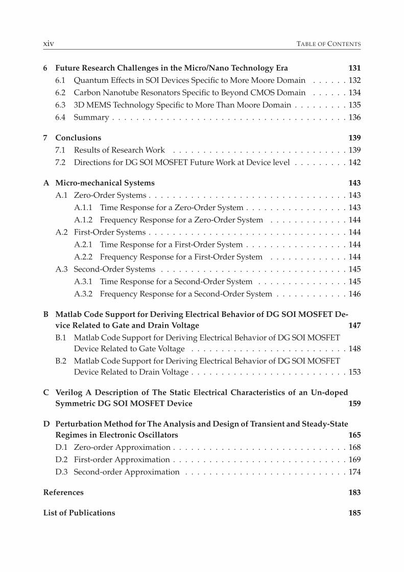
6 Future Research Challenges in the Micro/Nano Technology Era 131
6.1 Quantum Effects in SOI Devices Specific to More Moore Domain . . . . . . 132
6.2 Carbon Nanotube Resonators Specific to Beyond CMOS Domain . . . . . . 134
6.3 3D MEMS Technology Specific to More Than Moore Domain . . . . . . . . . 135
6.4 Summary . . . . . . . . . . . . . . . . . . . . . . . . . . . . . . . . . . . . . . . 136
7 Conclusions 139
7.1 Results of Research Work . . . . . . . . . . . . . . . . . . . . . . . . . . . . . 139
7.2 Directions for DG SOI MOSFET Future Work at Device level . . . . . . . . . 142
A Micro-mechanical Systems 143
A.1 Zero-Order Systems . . . . . . . . . . . . . . . . . . . . . . . . . . . . . . . . . 143
A.1.1 Time Response for a Zero-Order System . . . . . . . . . . . . . . . . . 143
A.1.2 Frequency Response for a Zero-Order System . . . . . . . . . . . . . 144
A.2 First-Order Systems . . . . . . . . . . . . . . . . . . . . . . . . . . . . . . . . . 144
A.2.1 Time Response for a First-Order System . . . . . . . . . . . . . . . . . 144
A.2.2 Frequency Response for a First-Order System . . . . . . . . . . . . . 144
A.3 Second-Order Systems . . . . . . . . . . . . . . . . . . . . . . . . . . . . . . . 145
A.3.1 Time Response for a Second-Order System . . . . . . . . . . . . . . . 145
A.3.2 Frequency Response for a Second-Order System . . . . . . . . . . . . 146
B Matlab Code Support for Deriving Electrical Behavior of DG SOI MOSFET De-
vice Related to Gate and Drain Voltage 147
B.1 Matlab Code Support for Deriving Electrical Behavior of DG SOI MOSFET
Device Related to Gate Voltage . . . . . . . . . . . . . . . . . . . . . . . . . . 148
B.2 Matlab Code Support for Deriving Electrical Behavior of DG SOI MOSFET
Device Related to Drain Voltage . . . . . . . . . . . . . . . . . . . . . . . . . . 153
C Verilog A Description of The Static Electrical Characteristics of an Un-doped
Symmetric DG SOI MOSFET Device 159
D Perturbation Method for The Analysis and Design of Transient and Steady-State
Regimes in Electronic Oscillators 165
D.1 Zero-order Approximation . . . . . . . . . . . . . . . . . . . . . . . . . . . . . 168
D.2 First-order Approximation . . . . . . . . . . . . . . . . . . . . . . . . . . . . . 169
D.3 Second-order Approximation . . . . . . . . . . . . . . . . . . . . . . . . . . . 174
References 183
List of Publications 185

List of Abbreviations
1D One Dimensional
3D Three Dimensional
AM Amplitude Modulation
BAW Bulk Acoustic Wave
BOX Burried Oxide
BTBT Band To Band Tunneling
CC Clamped-Clamped
CMOS Complementary Metal Oxide Semiconductor
CPU Control Processor Unit
CSE Charge Sharing Effect
DELTA DEpleted Lean-channel TrAnsistor
DG Double Gate
DIBL Drain-Induced Barrier Lowering
DT Direct Tunneling
FBAR Film Bulk Acoustic Resonator
FET Field Effect Transistor
FD Fully Depleted
FDD Frequency Division Duplexer
FF Free Free
FIJ Field Induced Junction
FN Fowler-Nordheim Tunneling
GAA Gate All Around
GIDL Gate Induced Drain Leakage
GSM Global System for Mobile Communication
IC Integrated Circuits
IF Intermediate Frequency
ITRS International Technology Roadmap for Semiconductors
JFET Junction Field Effect Transistor
LOCOS Local Oxidation of Silicon
LO Local Oscillation
xv
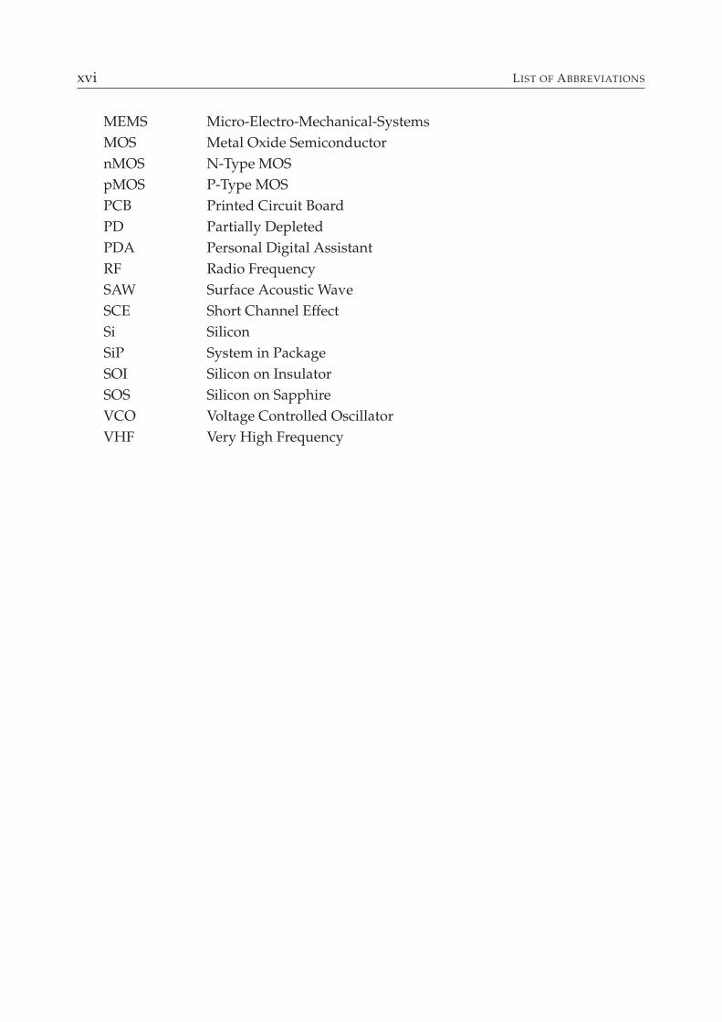
xvi LIST OF ABBREVIATIONS
MEMS Micro-Electro-Mechanical-Systems
MOS Metal Oxide Semiconductor
nMOS N-Type MOS
pMOS P-Type MOS
PCB Printed Circuit Board
PD Partially Depleted
PDA Personal Digital Assistant
RF Radio Frequency
SAW Surface Acoustic Wave
SCE Short Channel Effect
Si Silicon
SiP System in Package
SOI Silicon on Insulator
SOS Silicon on Sapphire
VCO Voltage Controlled Oscillator
VHF Very High Frequency

List of Symbols
b Damping coefficient
bc Critical damping coefficient
CDS Drain-source capacitance
CG Gate capacitance
CGS Gate-source capacitance
CGD Gate-drain capacitance
E Energy
EC Conduction band energy of a semiconductor
EF Fermi Energy
Eg Energy bandgap of a semiconductor
Ei Intrinsic Fermi energy
EV Valence band energy of a semiconductor
f Frequency
fmax Maximum frequency of oscillation
fT Cut-off frequency
gd (gout) Output conductance of a MOSFET
gm Transconductance of a MOSFET
km Mechanical Stiffness
ke Electrical Stiffness
I Current
ID Drain current
k Boltzmann’s constant
L Length
m Mass
n Electron density
ni Intrinsic carrier density
NA Acceptor doping density
p Hole density
q Electronic charge
xvii
xviii LIST OF SYMBOLS
Q Electrical charge
Qi Interface charge density per unit area
Qinv Inversion layer charge density per unit area
R Electrical resistance
tox Oxide thickness
tSi Silicon thickness
T Temperature
V Voltage
VD Drain voltage
VDS Drain-source voltage
VFB Flatband voltage
VG Gate voltage
VGS Gate-source voltage
Vt Thermal voltage
VT , Vth Threshold voltage of an MOS transistor
ǫox Dielectric constant of silicon-dioxide
ǫSi Dielectric constant of silicon
ǫ0 Dielectric constant of vacuum
µn Electron mobility
µp Hole mobility
ΦM Workfunction of a metal
ΦMS Workfunction difference between a metal and a semiconductor
ω Angular frequency
ΦS Workfunction of a semiconductor
ω0 Mechanical Resonant natural frequency
ξ Damping ratio
ψ Silicon electrostatic potential
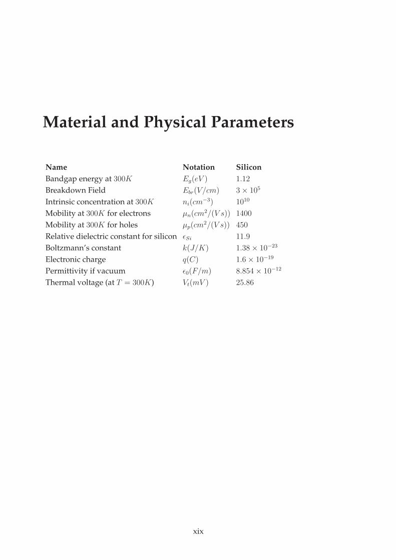
Material and Physical Parameters
Name Notation Silicon
Bandgap energy at 300K Eg(eV ) 1.12
Breakdown Field Ebr(V/cm) 3 × 10⁵
Intrinsic concentration at 300K ni(cm−3) 1010
Mobility at 300K for electrons µn(cm2/(V s)) 1400
Mobility at 300K for holes µp(cm2/(V s)) 450
Relative dielectric constant for silicon ǫSi 11.9
Boltzmann’s constant k(J/K) 1.38 × 10⁻²³
Electronic charge q(C) 1.6 × 10⁻¹⁹
Permittivity if vacuum ǫ0(F/m) 8.854 × 10⁻¹²
Thermal voltage (at T = 300K) Vt(mV ) 25.86
xix

List of Figures
2.1 The First Point-Contact Transistor. . . . . . . . . . . . . . . . . . . . . . . . . 7
2.2 Road-map for the Feature Size (source: ITRS). . . . . . . . . . . . . . . . . . 9
2.3 Moore’s Law and More (source: ITRS 2007) . . . . . . . . . . . . . . . . . . 9
2.4 Microprocessor and Frequency Roadmap (source: ITRS). . . . . . . . . . . 10
2.5 Voltage Roadmap (source: ITRS). . . . . . . . . . . . . . . . . . . . . . . . . 12
2.6 SOI MOSFET Roadmap (source: [27]). . . . . . . . . . . . . . . . . . . . . . 12
2.7 A cross view of a silicon on insulator transistor. . . . . . . . . . . . . . . . . . 13
2.8 Summary of leakage current mechanisms of deep-submicrometer transis-
tors (source: [101]). . . . . . . . . . . . . . . . . . . . . . . . . . . . . . . . . . 15
2.9 Log(ID) versus VG at two different drain voltages (0.1 V and 2.5 V ) for an
nMOSFET . (source: [101]). . . . . . . . . . . . . . . . . . . . . . . . . . . . . 16
2.10 The gate oxide tunneling processes and the hot-carrier injection from sub-
strate to oxide (source: [101]). . . . . . . . . . . . . . . . . . . . . . . . . . . . 18
2.11 Potential Profile inside the Silicon Film for (a) un-coupling interfaces (dop-
ing NA = 4 · 1016 cm−3, film thickness tSi = 300 nm) and (b) coupling
interfaces (NA = 3 · 1015 cm−3, tSi = 100 nm). x is the distance from the
front interface (source: [6]). . . . . . . . . . . . . . . . . . . . . . . . . . . . . . 22
2.12 A cross view for a partially depleted SOI MOSFET (source [29]). . . . . . 23
2.13 A cross view for a fully depleted SOI MOSFET (source [29]). . . . . . . . . 24
2.14 Sub-threshold slope in a multiple-gate SOI MOSFET as a function of gate
length (source: [26]). . . . . . . . . . . . . . . . . . . . . . . . . . . . . . . . . 24
2.15 A Double-Gate SOI MOSFET (source: [27]). . . . . . . . . . . . . . . . . . . 25
2.16 Sub-threshold Swing for various types of extremely thin SOI MOSFETs
with (VG2 = −40 V ) and without back gate accumulation (tox1 = 3 nm
and tox2 = 0.38 nm) and with a double gate structure for various doping
(source: [97]). . . . . . . . . . . . . . . . . . . . . . . . . . . . . . . . . . . . . 26
2.17 A Triple-Gate SOI MOSFET (source: [27]). . . . . . . . . . . . . . . . . . . . 27
2.18 Schematic view of a Surrounding-Gate SOI MOSFET (source: [27]). . . . . 27
xxi
xxii LIST OF FIGURES
2.19 Circuit diagram for the stacked inverters implemented with: a) Bulk and
b) Dg SOI MOSFET (source: [3]). . . . . . . . . . . . . . . . . . . . . . . . . 29
2.20 Dependence of the leakage current reduction factor due to transistor stack-
ing Istack/Idev on back-bias voltage VBB (source: [3]). . . . . . . . . . . . . . . 30
3.1 Micro-machining technology: bulk and surface [37]. . . . . . . . . . . . . . . 35
3.2 Perspective-view of an RF MEMS capacitor (source [125]). . . . . . . . . . 38
3.3 Cross-view of an RF MEMS capacitor with movable dielectric (source
[126]). . . . . . . . . . . . . . . . . . . . . . . . . . . . . . . . . . . . . . . . . . 38
3.4 Perspective-view of an RF MEMS inductor (source [125]). . . . . . . . . . . 39
3.5 Cross-view of an ohmic RF MEMS switch (source [125]). . . . . . . . . . . 40
3.6 Cross-view of a capacitive RF MEMS switch (source [125]). . . . . . . . . . 40
3.7 Perspective-view of a Clamped-Clamped Beam Resonator (source [65]). . . 41
3.8 Perspective-view of a Free-Free Beam Resonator (source [120]). . . . . . . . 43
3.9 Measured Frequency Characteristic of a Free-Free Beam Resonator (source
[120]). . . . . . . . . . . . . . . . . . . . . . . . . . . . . . . . . . . . . . . . . . 44
3.10 Cross-view of a Capacitive Comb Transduced Micro-resonator (source [88]). 45
3.11 Measured transconductance spectrum for a capacitive comb transduced
mirco-resonator that operates under a vacuum pressure of 20 mtorr (source
[79]). . . . . . . . . . . . . . . . . . . . . . . . . . . . . . . . . . . . . . . . . . 46
3.12 Perspective-view of a Radial-Contour Mode Risk Resonator (source [21]). . 47
3.13 Perspective-view of a Wine-Glass Disk Resonator (source [64]). . . . . . . . 51
3.14 Measured frequency characteristics of a wine glass disk resonator (source
[64]). . . . . . . . . . . . . . . . . . . . . . . . . . . . . . . . . . . . . . . . . . 52
3.15 Perspective-view of a Wine-Glass Ring Resonator (source [124]). . . . . . . . 52
3.16 Micro-mechanical ”Hollow-Disk” Ring Resonator (source [63]). . . . . . . . 53
3.17 Measured frequency characteristics for a micro-mechanical ”Hollow-Disk”
Ring Resonator under vacuum (source [63]). . . . . . . . . . . . . . . . . . . 54
3.18 Micro-electro-mechanical Antenna (source [69]). . . . . . . . . . . . . . . . . 55
3.19 a. Perspective-view of a Clamped-Clamped Micro-mechanical Filter; b.
Equivalent Mechanical Circuit (source [49, 90]) . . . . . . . . . . . . . . . . . 56
3.20 Equivalent Electric Circuit (source [49, 90]). . . . . . . . . . . . . . . . . . . . 57
3.21 Measured spectrum for 7.81 MHz micro-mechanical filter. (source [49]). . . 57
3.22 Perspective-view of a Bridged Micro-mechanical Filter (source [59]). . . . . 58
3.23 Perspective-view of a Mixer-Filter (source [122]). . . . . . . . . . . . . . . . . 59
3.24 Mixler Spectrum (source [122]). . . . . . . . . . . . . . . . . . . . . . . . . . . 60
LIST OF FIGURES xxiii
3.25 Schematic-view of a Series Resonant Oscillator Circuit (source [65]). . . . . . 61
3.26 Perspective-view of a Micro-mechanical Oscillator (source [88]). . . . . . . . 62
3.27 Schematic-view of a Channel Selector Filter Network (source [81]). . . . . . 63
3.28 Schematic-view of a Transceiver that uses Off-chip Components (source [90]). 64
3.29 Schematic-view of a Transceiver that uses On-chip Components. . . . . . . . 65
3.30 Schematic-view of a Transceiver with Switch-ableRF Channel Select Filter,
Switch-able Micro-mechanical Resonator Synthesizer and Micro-mechanical
Mixer-Filter. . . . . . . . . . . . . . . . . . . . . . . . . . . . . . . . . . . . . . 66
3.31 Schematic-view of a MEMS RF Front-End Transceiver. . . . . . . . . . . . 67
4.1 Schematic-cross section of a Double Gate SOI MOSFET structure. . . . . . 71
4.2 Schematic energy bands diagram for a Double Gate SOI MOSFET , at
thermodynamic equilibrium. . . . . . . . . . . . . . . . . . . . . . . . . . . . 71
4.3 Graphical method for the calculation of the electrostatic potential drop in
the center of the silicon body ψ0, when VGS = 0.5 V . The functions f and g
are dependent on ψ0 and VGS . . . . . . . . . . . . . . . . . . . . . . . . . . . . 75
4.4 The electrostatic potentials ψs and ψ0 as a function of VGS voltage. This
result was obtained with our graphical method for silicon thickness of 5
nm and 20 nm. . . . . . . . . . . . . . . . . . . . . . . . . . . . . . . . . . . . . 76
4.5 The electrostatic potentials as a function of gate to source and channel volt-
ages. . . . . . . . . . . . . . . . . . . . . . . . . . . . . . . . . . . . . . . . . . 78
4.6 The silicon electrostatic potential as a function of the channel voltage when
the gate voltage takes the values of 0.5 V , 1 V and 1.5 V . . . . . . . . . . . . 78
4.7 The variation of the electrostatic potential with the position in the silicon
film for the drain voltage equal to 0.5 V and 1 V . The gate voltage takes the
values of 0.6 V , 0.7 V and 1 V . . . . . . . . . . . . . . . . . . . . . . . . . . . . 79
4.8 The silicon electrostatic potentials as a function of gate to source voltage
VGS when the channel potential has different values, for asymmetric DG
SOI MOSFET transistor. . . . . . . . . . . . . . . . . . . . . . . . . . . . . . 84
4.9 The silicon electrostatic potentials as a function of channel voltage Vch when
the gate to source potential is 0.6 V . . . . . . . . . . . . . . . . . . . . . . . . . 84
4.10 The variation of the electrostatic potential with the position in the silicon
film, when the drain voltage is 0.5 V and 1 V , respectively. The gate voltage
is assumed to be equal to 0.5 V , 0.6 V and 0.9 V . . . . . . . . . . . . . . . . . 85
4.11 The position of the minimum silicon electrostatic potential as a function of
drain voltage when VGS varies in the range of [0.5; 1] V . . . . . . . . . . . . . 85
4.12 The carrier charge as a function of gate voltage and drain voltage, for sili-
con thicknesses of 5 nm, 10 nm and 20 nm. . . . . . . . . . . . . . . . . . . . . 87
xxiv LIST OF FIGURES
4.13 Output characteristics of the DG SOI MOSFET with VGS varying from
0.5 V to 1 V . . . . . . . . . . . . . . . . . . . . . . . . . . . . . . . . . . . . . . 88
4.14 Transconductance and Output Conductance for an un-doped symmetric
DG SOI MOSFET . . . . . . . . . . . . . . . . . . . . . . . . . . . . . . . . . 89
4.15 Schematic energy bands diagram of an asymmetric, un-doped DG SOI
MOSFET . . . . . . . . . . . . . . . . . . . . . . . . . . . . . . . . . . . . . . . 91
4.16 Domain of definition for both minimum electrostatic potential and its lo-
calization. . . . . . . . . . . . . . . . . . . . . . . . . . . . . . . . . . . . . . . 93
4.17 The minimum electrostatic potential as a function of the applied gate-to-
source voltage. . . . . . . . . . . . . . . . . . . . . . . . . . . . . . . . . . . . . 95
4.18 Electrostatic potential profile in the silicon body for VGS = 0.95 V . . . . . . . 95
4.19 Electrostatic potential profile in the silicon body for three arbitrary values
of the position of minimum electrostatic potential in the range from −0.5
nm to +0.5 nm around the center of silicon layer, but with constant ψ0. . . . 96
4.20 An asymmetric DG SOI nMOSFET with terminal voltages consisting of
a dc bias plus a time-varying signal. The same schematic can be used for
both large and small signal approaches. . . . . . . . . . . . . . . . . . . . . . 99
4.21 An asymmetricDGSOI nMOSFET with all four terminal-to-ground small
signal voltages equal. . . . . . . . . . . . . . . . . . . . . . . . . . . . . . . . . 105
4.22 A DG SOI nMOSFET with terminal voltages referenced to source. . . . . 106
4.23 The complete small signal circuit for an asymmetric DG SOI nMOSFET
device. . . . . . . . . . . . . . . . . . . . . . . . . . . . . . . . . . . . . . . . . 107
4.24 The complete small signal circuit for a symmetric DG SOI nMOSFET
device, at quasi-static operation. . . . . . . . . . . . . . . . . . . . . . . . . . 108
4.25 Terminal electric charges of a symmetric DG SOI nMOSFET , derived
with our analytical model. . . . . . . . . . . . . . . . . . . . . . . . . . . . . . 109
4.26 Normalized capacitances of a symmetric DG SOI nMOSFET , derived
with our analytical model. . . . . . . . . . . . . . . . . . . . . . . . . . . . . . 110
4.27 a. The DG SOI nMOSFET used in a common source configuration; b The
small-signal circuit for the DG SOI nMOSFET used as a circuit. . . . . . . 111
4.28 The variation of cutoff frequency as a function of VGS , calculated with the
analytical model. . . . . . . . . . . . . . . . . . . . . . . . . . . . . . . . . . . 112
4.29 Simplified Small-Signal Circuit of the common source configuration from
Figure 4.27a. . . . . . . . . . . . . . . . . . . . . . . . . . . . . . . . . . . . . . 112
5.1 Comparison of the Output Characteristics for an Un-doped SymmetricDG
SOI MOSFET performed with Matlab and Verilog A. . . . . . . . . . . . . 116
LIST OF FIGURES xxv
5.2 Common Source Amplifier Based on DG SOI MOSFET implemented in
Verilog A. . . . . . . . . . . . . . . . . . . . . . . . . . . . . . . . . . . . . . . . 117
5.3 Transfer Characteristic (Vout = f(Vin)) for a Common Source Amplifier
Based on DG SOI MOSFET implemented in Verilog A based on our de-
veloped models. . . . . . . . . . . . . . . . . . . . . . . . . . . . . . . . . . . . 117
5.4 Integrated RF MEMS and DG SOI MOSFET Based Oscillator. . . . . . . 119
5.5 Small signal equivalent circuit and incremental circuit for an RF MEMS
and DG SOI MOSFET based oscillator. . . . . . . . . . . . . . . . . . . . . 120
5.6 Amplitude Envelope of the fundamental harmonic as a function of time for
the case of first order approximation of the integrated Colpitts oscillator
based on RF MEMS resonator.. . . . . . . . . . . . . . . . . . . . . . . . . . 128
5.7 Variation of the normalized oscillation frequency as a function of time dur-
ing transient regime, as predicted by the second order approximation. . . . 129
6.1 Moore’s Law and More (source: ITRS 2007). . . . . . . . . . . . . . . . . . . 132
6.2 Influence of the silicon thickness on the electron concentration distribution
at the surface potential constant, according to the quantum model (source:
[72]). . . . . . . . . . . . . . . . . . . . . . . . . . . . . . . . . . . . . . . . . . 133
6.3 Discrete energy levels Eij of electrons in the semiconductor conduction
band for a symmetrical DG SOI MOSFET structure (source: [72]). . . . . . 134
6.4 Schematic of the CNT -based AM demodulator (source: [102]). . . . . . . . . 134
6.5 Equivalent circuit for the CNT resonator (source: [58]). . . . . . . . . . . . . 135
6.6 Different generations of silicon-based SiP modules using 3D die stacking
and packaging (source: Solid State Technology). . . . . . . . . . . . . . . . . 136
A.1 MEMS Resonator. . . . . . . . . . . . . . . . . . . . . . . . . . . . . . . . . . . 145

Chapter 1
Introduction
1.1 Motivation
In the last decades, continuous needs of industrial process automation and people’s in-
creased desire for lifestyle, safety, security and real-time interconnectivity have been the
driving force for the unprecedented development of all industrial processes and con-
sumer electronics. In the same time, the technology of semiconductors has made an im-
pressive progress, to respond to the above challenging market demands. As predicted
by Gordon Moore, from 1965, the silicon integrated circuit (IC) technology has shown a
continuous down-scaling of theMOSFET transistor dimensions in order to reach higher
packing density, performances improvement, faster circuit speed and lower power con-
sumption. To attain these goals, for both consumer electronics and industrial environ-
ment, the designers have made big efforts to improve the power-efficiency, reduce the
sizes and fulfill the increased integrability. Thus, the continuous efforts of chip makers to
respond to market requirements and emerging new applications have lead year by year
to new integrated circuits with complex functions on the same chip. After this more than
four decades scaling-down journey, the bulk CMOS technology will reach the end of
the road-map due to the increase in short channel effects which limited the device’s low
power operation. Thus, the Silicon on Insulator (SOI) CMOS technology appeared as a
promising alternative for bulk CMOS to obtain new devices with superior advantages
in terms of: 1) light doping of the channel for mobility improvement; 2) good control
of short channel effects by increased electrostatic control due to the voltage applied on
multiple gates (dual gate-DG, three gates-TG, gates all around-GAA); 3) almost ideal
sub-threshold slope due to the elimination of substrate doping; 4) increased current drive
capability due to the volume inversion [6] of the entire silicon film. However, some chal-
lenges exist in terms of 3D technological complexity and ultra thin silicon film needed for
these SOI MOSFET devices.
On the other hand, almost in the same time with IC technology birth, the first micro-
electro-mechanical systems (MEMS) have been developed on the silicon wafer, making
1
2 CHAPTER 1 INTRODUCTION
thus possible on-chip processing of non-electrical signal for sensing and actuating pur-
poses. It was just only a matter of time, till the IC technology married with MEMS
technology to generate the first on-chip integrated MEMS, marking thus the beginning
of a new technology revolution (as shown by the first integrated pressure sensors), that
is bursting, now. An important branch of MEMS is the RF MEMS, where many sep-
arate components, like antenna, passive and active RF components can be performed
on silicon chip. This new emerging field of RF MEMS will revolutionize the wireless
electronics by the potential of the vibrating micro-mechanical circuits to operate at high
quality factor, enabling the on-chip multiple signal processing and the integration of RF
MEMS on the same chip with CMOS integrated circuits. It is the purpose of this thesis
to open new bridges between the ultimate SOI MOSFET technology and the emerg-
ing RF MEMS field, trying to show by analytical methods how the new family of dual
gate DG SOI MOSFET devices operate in the dc and ac regime and how one can use
them for developing an integrated MEMS oscillator as modeling example of the future
integrated DG SOI-MOSFET -RF MEMS systems.
The above topic is in agreement with the research objectives of our university group
in the field of the analog device and circuit modeling, as well as with the scientific target
of the organization called TICMO (Tunable Integrable Components in Microwave Tech-
nology and Optics). It aims the synergetic multidisciplinary interaction between many
specialists and their teams working on tunable or frequency-agile components having a
major and extensive operational potential in communication and sensor systems.
Very briefly speaking, within my thesis, a detailed analytical modeling of dc and ac
regimes of the Double-Gate SOI MOSFET will be realized and, then, these models will
be used for developing a perturbation method-based methodology of design for a RF
MEMS based oscillator that contains the RF MEMS resonator in its positive feedback-
loop.
1.2 Research Objectives
This dissertation is focused on next generation of SOI MOSFET devices aiming contri-
butions to the analytical compact modeling of Dual Gate SOI MOSFET and potential
application of these new devices to wireless RF MEMS systems. An integrated oscil-
lator build with a DG SOI MOSFET device and a RF MEMS circuit in its positive
feed-back loop is analytical modeled and designed to prove the use of these DG SOI
MOSFET devices for future applications. For this purpose, the state of the art in mod-
eling and technology of SOI MOSFET devices and the RF micro-electro-mechanical
systems are thoroughly investigated. The objectives of the thesis can be summarized as
follow:
• to offer a dc analytical compact modeling of a DG SOI MOSFET founded on the
classical physics concepts, by proposing simple and convenient methods to calcu-
1.3 THESIS OUTLINE 3
late the silicon electrostatic potentials and then, the drain current, transconductance
and output conductance;
• to propose an ac top-down methodology in order to derive the entire small signal
equivalent circuit for a DG SOI MOSFET for which, the terminal charges and ca-
pacitances are going to be calculated by using the method proposed in the previous
part. The main device figures of merit such as cut-off frequency and maximum
frequency of oscillation will be then calculated;
• to provide a hardware description in Verilog-A for the above-proposed model of an
un-doped symmetrical DG SOI MOSFET ;
• to offer an insight into the micro-electro-mechanical systems evolution and develop
an electrical equivalent model for an RF MEMS resonator;
• to design a common-source amplifier which contains theDGSOI MOSFET device
implemented in Verilog-A behavioral language;
• to propose a new Colpitts oscillator formed on a DG SOI MOSFET and the equiv-
alent RLC electrical circuit of the RF MEMS resonator presented previously.
1.3 Thesis Outline
The thesis is organized in three main parts. The introduction consists of a motivation,
problem formulation and state of the art of SOI and RF MEMS devices. Then, the core
chapters contain my original contributions to the dc and ac un-dopedDGSOI MOSFET
modeling and its implementation in Verilog A tool. The work continues with the design
of a DG SOI MOSFET - and RF MEMS-based oscillator. Finally, the thesis concludes
with the presentation of the future work and summary of the current research. The three
main parts of the thesis are described below, as follows:
I - Background Chapters 2 and 3 present the state of the art in the silicon-based de-
vices and micro-electro-mechanical systems evolution. The goal of the chapter 2 is
to present the MOSFET transistor evolution by describing the gradual transition
from silicon bulk technology to the silicon-on-insulator technology and emphasiz-
ing their advantages and challenges. The limiting short channel effects and the leak-
age currents inMOS transistors will be presented in this chapter together with their
main overcoming solutions that include the silicon-on-insulator devices. Once that
SOI technology environment is completed, chapter 3 poses the benefits and chal-
lenges of the new vibrating RF MEMS devices and circuits made with the micro-
machining technology which can be applicable at different future portable and/or
wireless communication applications. For this purpose, the RF MEMS devices
are enumerated and presented by emphasizing their main functions accomplished
4 CHAPTER 1 INTRODUCTION
when they are connected together and then describing the most important circuits
used in wireless communication applications. Besides, the evolution of transceiver
architectures is included, starting from the present generation where CMOS inte-
grated circuits interface at the board level with off-chip quartz-based passive com-
ponents for getting transceiver architectures performed on printed circuit board
(PCB) and ending up with an ultimate vision of an all-MEMS transceiver in which
all the above-mentioned MEMS elements are located on a single silicon chip to-
gether with the electronic RF circuits.
II - Personal Contributions The chapters 4 and 5 represent the core of the work. Once
the general environment of SOI MOSFET devices is created, an important aspect
is to understand and model a particular SOI transistor, called Double-Gate SOI
MOSFET . Since the phenomena are more complex due to the increased number
of gates that surround the silicon substrate, the chapter 4 of the thesis addresses
the DC analytical modeling of un-doped double-gate SOI MOSFET by proposing
convenient and simple methods to calculate the device electrical parameters such as:
electrostatic potentials, electric charges, drain current, transconductance and output
conductance. Further, the AC analysis of an un-doped symmetric SOI MOSFET
device is proposed beginning with the derivation of the small-signal equivalent cir-
cuit, continuing with the evaluation of terminal charges and capacitances and end-
ing with the calculation of the RF figures of merits such as cut-off frequency and
maximum frequency of oscillation. The entire analytical model is implemented in
Verilog A Language and presented in chapter 5. The efficiency of this code is shown
by realizing an application in terms of a common source amplifier based on the DG
SOI MOSFET transistor. In addition, a Colpitts oscillator is going to be designed
in the time domain, by means of a perturbation method and taking into account the
electrical characteristics of novelDG SOI MOSFET device and an equivalentRLC
electrical circuit of a micro-mechanical resonator.
III - Forward Plan Finally, the future work and conclusions are described in the last two
chapters. Since the thesis deals with two great research directions of silicon-based
areas in terms ofDGSOI MOSFET devices andRF MEMS components and their
future linkage, the chapter 6 focuses on the next challenges in the field, where micro
(like 3D MEMS) and nano-technology (like CNT based nano devices and circuits)
will be together on the same ultra small chip for increased functionality. Finally, in
chapter 7 the dissertation presents a summary of the contributions provided by the
present work.
Chapter 2
Evolution of the SOI MOSFET Devices
for Integrated Circuits
During the last decades, the MOSFET transistor dimensions have been in a continuous
aggressive down-scaling in order to reach higher packing density, faster circuit speed and
lower power consumption. The perpetual efforts of chip makers to respond to the market
requirements and new applications have lead year by year to new integrated circuits with
complex functions on the same chip. During this time the bulk CMOS technology has
shown its ability to respond to the above challenges, but in the next decade this CMOS
technology will reach the end of the road-map. In the shadow of the CMOS big brother,
the SOI (semiconductor on silicon, in the most general definition) technology has grown
up steadily, proving recently its maturity when the first commercial SOI microprocessors
appeared on the market. More than that, the SOI technology will be taken over as an
alternative to bulk CMOS, when the last one is giving up in terms of scalability, material
flexibility and minimum feature size of transistor.
The main objective of this chapter is to describe the smooth transition from silicon bulk
technology to the silicon-on-insulator technology, by emphasizing their advantages and
challenges. The current chapter begins with the history of the electron devices starting
from the invention of the solid state rectifier and ending with the present devices. The
scaling down rules, which have made the Moore’s law to become so true for more than
four decades will be described here, as well as silicon technology road-map showing the
device miniaturization as a function of time in the dimension range from 10 microns to
10 nm. The limiting short channel effects and the leakage currents in MOS transistors,
which have been threatening the scaling process at each new technology node, have been
constantly solved by creative technologists and designers and, thus, making possible the
progress we have today. Afterward, the silicon-on-insulator evolution will be described
by presenting the most important devices made with this technology. The integrated
circuit based on double-gate silicon on insulator MOSFET transistor will be included,
followed by a short description of future challenges.
5
6 CHAPTER 2 EVOLUTION OF THE SOI MOSFET DEVICES FOR INTEGRATED CIRCUITS
2.1 The Transition from the Bulk MOSFET Devices to Multi-
Gate SOI MOSFET Devices
2.1.1 History of Electron Devices
The history of semiconductor devices goes back to the year 1874, when Ferdinand Braun
invented the solid state rectifier, which was based on point contact in lead sulfide [11].
By that time the solid state physics and electronics had no theoretical basis. The quantum
mechanics theory and its application to solid material accelerated the progress of solid
electronics. In 1900, Max Plank presented his theory of quantum energy, where the energy
unit was called quanta and the energy being a multiple of quanta. According to it, the
electron is not free to have every energy in the solid state, but different levels of energy.
This approach helped later understanding the energy band structures in solid materials
and thus, differentiate them as metals, insulators and semiconductors.
In parallel, at the beginning of 1900 year, the direction of vacuum tube was investi-
gated. Actually, the father of vacuum technology, should be considered Thomas Edison,
who has invented the light bulb which was the first vacuum tube used for the electrical
applications. In 1906, Lee De Forest made the vacuum tube triode that had three termi-
nals and amplified the audio signals, making AM radio possible. The vacuum tube or
electron tube represents the first device used to amplify electronic signals and this played
an important role in the development of the electronic circuits and vacuum technology
as well as the system and computer science. The first computer was performed with
vacuum tubes and occupied a few rooms. This is why we say today that the vacuum
electronics suffered from large occupied volume, high power consumption and reliability
issues, even if it was so important by that time.
Then, the final mathematical formulation of the quantum mechanic approach was de-
veloped in 1920, while its application to solid state was done by Mott and other scientists
from UK. It is worth to mention that the concept of a field effect transistor (FET ) was
invented by Lilienfeld in 1926. He was the first who sayed that applying an electrical
field on a poorly conducting material, you can change its electrical conductivity. Unfor-
tunately, the concept was not successfully demonstrated at that time, due to the techno-
logical problems related to the control and reduction of the surface states at the interface
between the oxide and the semiconductor. At the end of 1930’s, Mervin Kelly from Bell
Labs decided to reinforce the solid state device research and he has made a team hav-
ing Robert Shockley, Russell Ohl and others, aiming to push electronics beyond vacuum
tubes. Similar work was done in Germany, by Pohl and Hilsch contriving the solid am-
plifier based on potassium bromide, and having three metal leads. At Bells labs, the first
successful decision was the selection of silicon and germanium as semiconductors crys-
tals. Thus, in 1940, Russel Ohl investigated silicon crystals and discovered the n- and p-
type silicon semiconductor, in terms of rectifying negative or positive ac signals. He, also,
built a sample in which the top part constituted a p- type region and the bottom was n−
2.1 THE TRANSITION FROM THE BULK MOSFET DEVICES TO MULTI-GATE SOI MOSFET DEVICES 7
type. When the light shone on the pn structure, he observed a voltage drop on the termi-
nals. After the second world war, the team from Bells included John Bardeen and Walter
Brattain, among other scientists working at understanding fundamentals of surface states
and its negative impact on the electrical behavior of semiconductors.
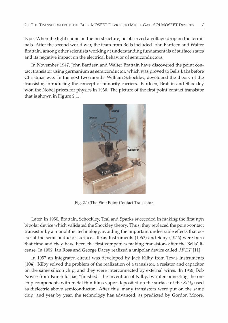
In November 1947, John Bardeen and Walter Brattain have discovered the point con-
tact transistor using germanium as semiconductor, which was proved to Bells Labs before
Christmas eve. In the next two months William Schockley, developed the theory of the
transistor, introducing the concept of minority carriers. Bardeen, Bratain and Shockley
won the Nobel prices for physics in 1956. The picture of the first point-contact transistor
that is shown in Figure 2.1.
Fig. 2.1: The First Point-Contact Transistor.
Later, in 1950, Brattain, Schockley, Teal and Sparks succeeded in making the first npn
bipolar device which validated the Shockley theory. Thus, they replaced the point-contact
transistor by a monolithic technology, avoiding the important undesirable effects that oc-
cur at the semiconductor surface. Texas Instruments (1952) and Sony (1955) were born
that time and they have been the first companies making transistors after the Bells’ li-
cense. In 1952, Ian Ross and George Dacey realized a unipolar device called JFET [11].
In 1957 an integrated circuit was developed by Jack Kilby from Texas Instruments
[104]. Kilby solved the problem of the realization of a transistor, a resistor and capacitor
on the same silicon chip, and they were interconnected by external wires. In 1959, Bob
Noyce from Fairchild has ”finished” the invention of Kilby, by interconnecting the on-
chip components with metal thin films vapor-deposited on the surface of the SiO2 used
as dielectric above semiconductor. After this, many transistors were put on the same
chip, and year by year, the technology has advanced, as predicted by Gordon Moore.
8 CHAPTER 2 EVOLUTION OF THE SOI MOSFET DEVICES FOR INTEGRATED CIRCUITS
Nowadays, these chips can be seen in computers, video cameras, cellular-phones, copy
machines, jumbo jets, modern automobiles, manufacturing equipment, electronic score-
boards and video games.
The first field-effect transistor namedMOSFET was fabricated in the years of 1960 by
Duane Kahng, by using Atalla’s oxidation process. After the identification of sodium ions
as the source of threshold voltage instability, the progress of MOS transistor technology
has been accelerated.
In November 1971, the world’s first single chip microprocessor, called Intel 4004, was
invented by Federico Faggin, Ted Hoff and Stan Mazor from Intel company. They devel-
oped it with 2300 transistors in an area of only 3 by 4 mm.
2.1.2 Technology Roadmap from Bulk MOSFET to SOI MOSFET
Nowadays, the silicon chips and integrated circuits are everywhere, from industrial pro-
cess control, till automotive and consumer electronics/wireless communication. The con-
sumer electronics is a strong driver today, asking for smaller, faster, low power IC and
with many functions implemented on the same chip, including wireless portable appli-
cations. The IC are expected to satisfy the society needs in all the fields, where health,
mobility, security, communication, entertainment and education are just examples [127].
The Moore’s law dates back to 19 April 1965 and it was presented in the article ”Cram-
ming more components onto integrated circuits” published in the Electronics magazine,
by McGraw-Hill editure [104]. Its author, Gordon E. Moore predicted that the number
of transistors per each integrated circuit chip (the so-called microprocessor performance)
would continue to double periodically, at every 24 months. So that, a memory with a
density of 65000 components was in production at Intel, ten years later, in agreement
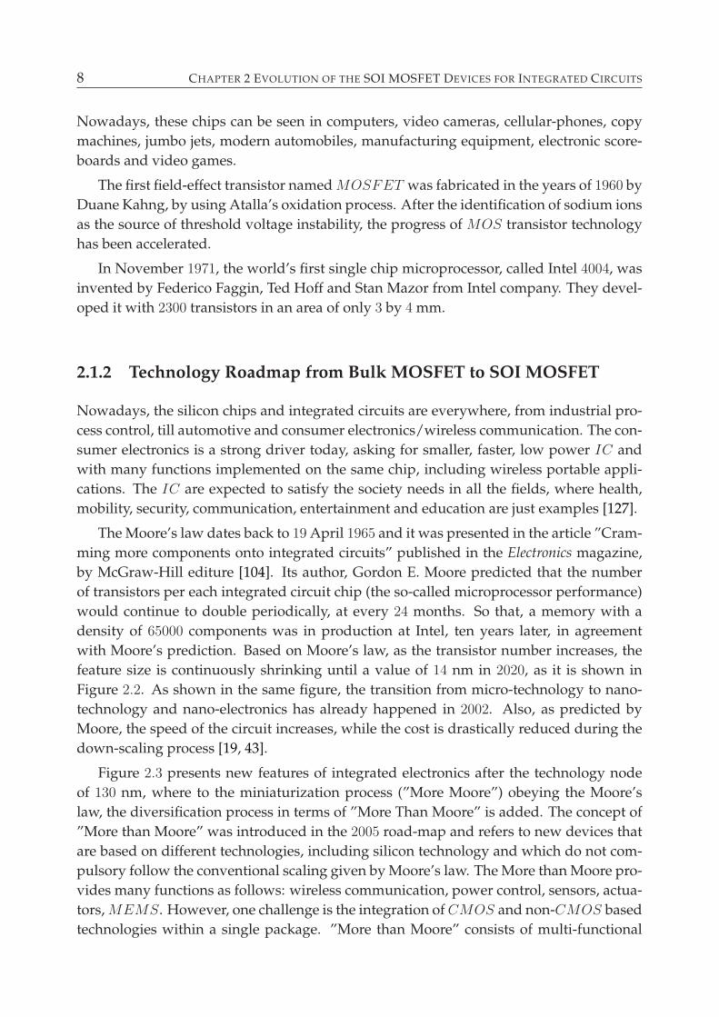
with Moore’s prediction. Based on Moore’s law, as the transistor number increases, the
feature size is continuously shrinking until a value of 14 nm in 2020, as it is shown in
Figure 2.2. As shown in the same figure, the transition from micro-technology to nano-
technology and nano-electronics has already happened in 2002. Also, as predicted by
Moore, the speed of the circuit increases, while the cost is drastically reduced during the
down-scaling process [19, 43].
Figure 2.3 presents new features of integrated electronics after the technology node
of 130 nm, where to the miniaturization process (”More Moore”) obeying the Moore’s
law, the diversification process in terms of ”More Than Moore” is added. The concept of
”More than Moore” was introduced in the 2005 road-map and refers to new devices that
are based on different technologies, including silicon technology and which do not com-
pulsory follow the conventional scaling given by Moore’s law. The More than Moore pro-
vides many functions as follows: wireless communication, power control, sensors, actua-
tors,MEMS. However, one challenge is the integration ofCMOS and non-CMOS based
technologies within a single package. ”More than Moore” consists of multi-functional
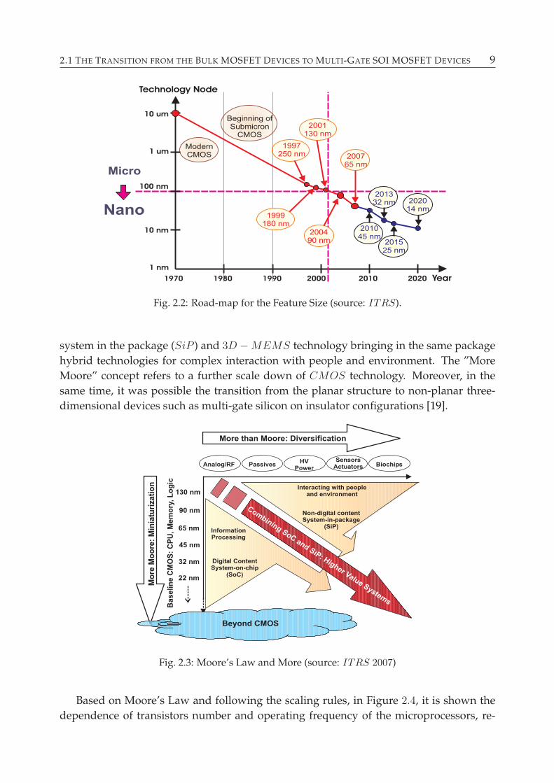
2.1 THE TRANSITION FROM THE BULK MOSFET DEVICES TO MULTI-GATE SOI MOSFET DEVICES 9
Fig. 2.2: Road-map for the Feature Size (source: ITRS).
system in the package (SiP ) and 3D −MEMS technology bringing in the same package
hybrid technologies for complex interaction with people and environment. The ”More
Moore” concept refers to a further scale down of CMOS technology. Moreover, in the
same time, it was possible the transition from the planar structure to non-planar three-
dimensional devices such as multi-gate silicon on insulator configurations [19].
More than Moore: Diversification
Mo
re M
oo
re:
Min
iatu
rizati
on
Analog/RF PassivesHV
Power
SensorsActuators Biochips
InformationProcessing
Digital ContentSystem-on-chip
(SoC)
Interacting with peopleand environment
Non-digital contentSystem-in-package
(SiP)
Beyond CMOS
Combining
SoCand
SiP: Higher ValueSystem
s
32 nm
22 nm
45 nm
90 nm
65 nm
130 nm
Ba
se
lin
e C
MO
S:
CP
U,
Me
mo
ry,
Lo
gic
Fig. 2.3: Moore’s Law and More (source: ITRS 2007)
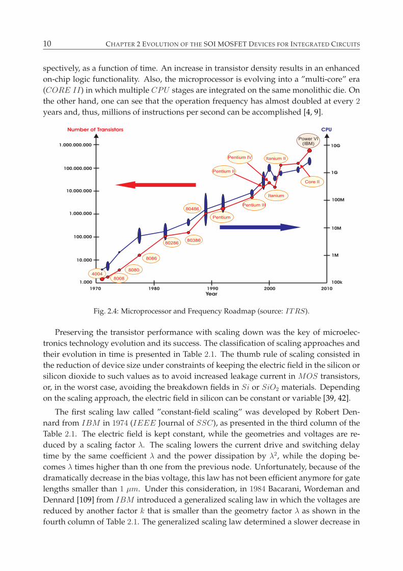
Based on Moore’s Law and following the scaling rules, in Figure 2.4, it is shown the
dependence of transistors number and operating frequency of the microprocessors, re-
10 CHAPTER 2 EVOLUTION OF THE SOI MOSFET DEVICES FOR INTEGRATED CIRCUITS
spectively, as a function of time. An increase in transistor density results in an enhanced
on-chip logic functionality. Also, the microprocessor is evolving into a ”multi-core” era
(CORE II) in which multiple CPU stages are integrated on the same monolithic die. On
the other hand, one can see that the operation frequency has almost doubled at every 2
years and, thus, millions of instructions per second can be accomplished [4, 9].
Fig. 2.4: Microprocessor and Frequency Roadmap (source: ITRS).
Preserving the transistor performance with scaling down was the key of microelec-
tronics technology evolution and its success. The classification of scaling approaches and
their evolution in time is presented in Table 2.1. The thumb rule of scaling consisted in
the reduction of device size under constraints of keeping the electric field in the silicon or
silicon dioxide to such values as to avoid increased leakage current in MOS transistors,
or, in the worst case, avoiding the breakdown fields in Si or SiO2 materials. Depending
on the scaling approach, the electric field in silicon can be constant or variable [39, 42].
The first scaling law called ”constant-field scaling” was developed by Robert Den-
nard from IBM in 1974 (IEEE Journal of SSC), as presented in the third column of the
Table 2.1. The electric field is kept constant, while the geometries and voltages are re-
duced by a scaling factor λ. The scaling lowers the current drive and switching delay
time by the same coefficient λ and the power dissipation by λ2, while the doping be-
comes λ times higher than th one from the previous node. Unfortunately, because of the
dramatically decrease in the bias voltage, this law has not been efficient anymore for gate
lengths smaller than 1 µm. Under this consideration, in 1984 Bacarani, Wordeman and
Dennard [109] from IBM introduced a generalized scaling law in which the voltages are
reduced by another factor k that is smaller than the geometry factor λ as shown in the
fourth column of Table 2.1. The generalized scaling law determined a slower decrease in
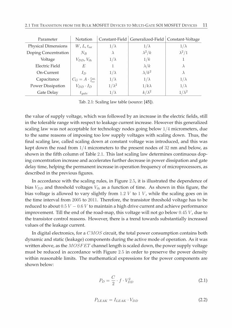
2.1 THE TRANSITION FROM THE BULK MOSFET DEVICES TO MULTI-GATE SOI MOSFET DEVICES 11
Parameter Notation Constant-Field Generalized-Field Constant-Voltage
Physical Dimensions W , L, tox 1/λ 1/λ 1/λ
Doping Concentration NB λ λ2/k λ2/1
Voltage VDD, Vth 1/λ 1/k 1
Electric Field E 1 λ/k λ
On-Current ID 1/λ λ/k2 λ
Capacitance CG = A · εoxtox
1/λ 1/λ 1/λ
Power Dissipation VDD · ID 1/λ2 1/kλ 1/λ
Gate Delay tgate 1/λ k/λ2 1/λ2
Tab. 2.1: Scaling law table (source: [45]).
the value of supply voltage, which was followed by an increase in the electric fields, still
in the tolerable range with respect to leakage current increase. However this generalized
scaling law was not acceptable for technology nodes going below 1/4 micrometers, due
to the same reasons of imposing too low supply voltages with scaling down. Thus, the
final scaling law, called scaling down at constant voltage was introduced, and this was
kept down the road from 1/4 micrometers to the present nodes of 32 nm and below, as
shown in the fifth column of Table 2.1. This last scaling law determines continuous dop-
ing concentration increase and accelerates further decrease in power dissipation and gate
delay time, helping the permanent increase in operation frequency of microprocessors, as
described in the previous figures.
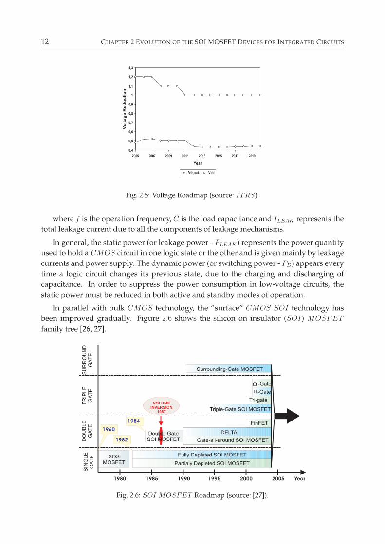
In accordance with the scaling rules, in Figure 2.5, it is illustrated the dependence of
bias VDD and threshold voltages Vth as a function of time. As shown in this figure, the
bias voltage is allowed to vary slightly from 1.2 V to 1 V , while the scaling goes on in
the time interval from 2005 to 2011. Therefore, the transistor threshold voltage has to be
reduced to about 0.5 V − 0.6 V to maintain a high drive current and achieve performance
improvement. Till the end of the road-map, this voltage will not go below 0.45 V , due to
the transistor control reasons. However, there is a trend towards substantially increased
values of the leakage current.
In digital electronics, for a CMOS circuit, the total power consumption contains both
dynamic and static (leakage) components during the active mode of operation. As it was
written above, as theMOSFET channel length is scaled down, the power supply voltage
must be reduced in accordance with Figure 2.5 in order to preserve the power density
within reasonable limits. The mathematical expressions for the power components are
shown below:
PD =C
2· f · V 2
DD (2.1)
PLEAK = ILEAK · VDD (2.2)
12 CHAPTER 2 EVOLUTION OF THE SOI MOSFET DEVICES FOR INTEGRATED CIRCUITS
Fig. 2.5: Voltage Roadmap (source: ITRS).
where f is the operation frequency, C is the load capacitance and ILEAK represents the
total leakage current due to all the components of leakage mechanisms.
In general, the static power (or leakage power - PLEAK) represents the power quantity
used to hold a CMOS circuit in one logic state or the other and is given mainly by leakage
currents and power supply. The dynamic power (or switching power - PD) appears every
time a logic circuit changes its previous state, due to the charging and discharging of
capacitance. In order to suppress the power consumption in low-voltage circuits, the
static power must be reduced in both active and standby modes of operation.
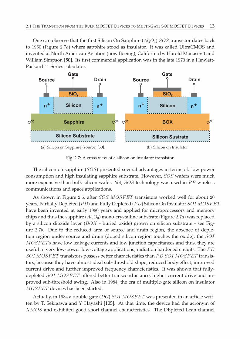
In parallel with bulk CMOS technology, the ”surface” CMOS SOI technology has
been improved gradually. Figure 2.6 shows the silicon on insulator (SOI) MOSFET
family tree [26, 27].
Fig. 2.6: SOI MOSFET Roadmap (source: [27]).
2.1 THE TRANSITION FROM THE BULK MOSFET DEVICES TO MULTI-GATE SOI MOSFET DEVICES 13
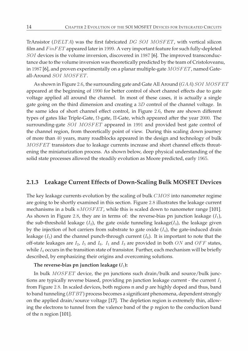
One can observe that the first Silicon On Sapphire (Al2O3) SOS transistor dates back
to 1960 (Figure 2.7a) where sapphire stood as insulator. It was called UltraCMOS and
invented at North American Aviation (now Boeing), California by Harold Manasevit and
William Simpson [50]. Its first commercial application was in the late 1970 in a Hewlett-
Packard 41-Series calculator.
(a) Silicon on Sapphire (source: [50]) (b) Silicon on Insulator
Fig. 2.7: A cross view of a silicon on insulator transistor.
The silicon on sapphire (SOS) presented several advantages in terms of: low power
consumption and high insulating sapphire substrate. However, SOS wafers were much
more expensive than bulk silicon wafer. Yet, SOS technology was used in RF wireless
communications and space applications.
As shown in Figure 2.6, after SOS MOSFET transistors worked well for about 20
years, Partially Depleted (PD) and Fully Depleted (FD) Silicon On Insulator SOI MOSFET
have been invented at early 1980 years and applied for microprocessors and memory
chips and thus the sapphire (Al2O3) mono-crystalline substrate (Figure 2.7a) was replaced
by a silicon dioxide layer (BOX - buried oxide) grown on silicon substrate - see Fig-
ure 2.7b. Due to the reduced area of source and drain region, the absence of deple-
tion region under source and drain (doped silicon region touches the oxide), the SOI
MOSFETs have low leakage currents and low junction capacitances and thus, they are
useful in very low-power low-voltage applications, radiation hardened circuits. The FD
SOI MOSFET transistors possess better characteristics than PD SOI MOSFET transis-
tors, because they have almost ideal sub-threshold slope, reduced body effect, improved
current drive and further improved frequency characteristics. It was shown that fully-
depleted SOI MOSFET offered better transconductance, higher current drive and im-
proved sub-threshold swing. Also in 1984, the era of multiple-gate silicon on insulator
MOSFET devices has been started.
Actually, in 1984 a double-gate (DG) SOI MOSFET was presented in an article writ-
ten by T. Sekigawa and Y. Hayashi [105]. At that time, the device had the acronym of
XMOS and exhibited good short-channel characteristics. The DEpleted Lean-channel
14 CHAPTER 2 EVOLUTION OF THE SOI MOSFET DEVICES FOR INTEGRATED CIRCUITS
TrAnsistor (DELTA) was the first fabricated DG SOI MOSFET , with vertical silicon
film andFinFET appeared later in 1999. A very important feature for such fully-depleted
SOI devices is the volume inversion, discovered in 1987 [6]. The improved transconduc-
tance due to the volume inversion was theoretically predicted by the team of Cristoloveanu,
in 1987 [6], and proven experimentally on a planar multiple-gateMOSFET , named Gate-
all-Around SOI MOSFET .
As shown in Figure 2.6, the surrounding gate and Gate All Around (GAA) SOI MOSFET
appeared at the beginning of 1990 for better control of short channel effects due to gate
voltage applied all around the channel. In most of these cases, it is actually a single
gate going on the third dimension and creating a 3D control of the channel voltage. In
the same idea of short channel effect control, in Figure 2.6, there are shown different
types of gates like Triple-Gate, Ω-gate, Π-Gate, which appeared after the year 2000. The
surrounding-gate SOI MOSFET appeared in 1991 and provided best gate control of
the channel region, from theoretically point of view. During this scaling down journey
of more than 40 years, many roadblocks appeared in the design and technology of bulk
MOSFET transistors due to leakage currents increase and short channel effects threat-
ening the miniaturization process. As shown below, deep physical understanding of the
solid state processes allowed the steadily evolution as Moore predicted, early 1965.
2.1.3 Leakage Current Effects of Down-Scaling Bulk MOSFET Devices
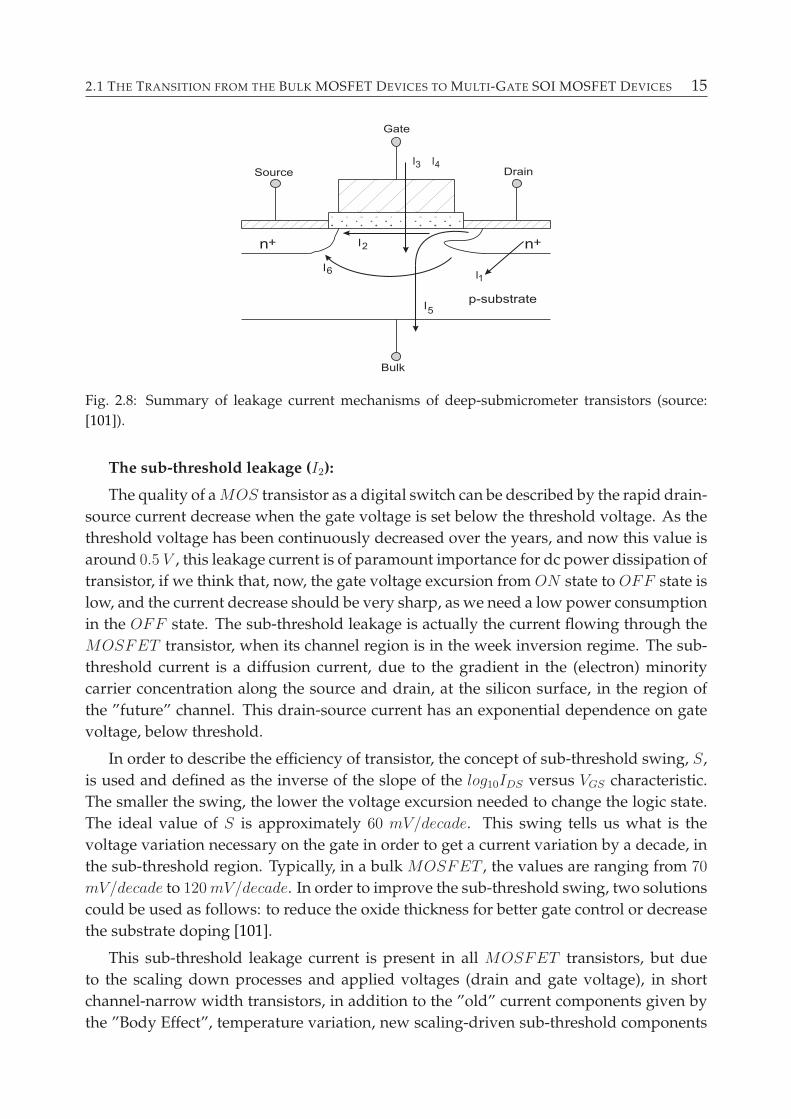
The key leakage currents evolution by the scaling of bulk CMOS into nanometer regime
are going to be shortly examined in this section. Figure 2.8 illustrates the leakage current
mechanisms in a bulk nMOSFET , while this is scaled down to nanometer range [101].
As shown in Figure 2.8, they are in terms of: the reverse-bias pn junction leakage (I1),
the sub-threshold leakage (I2), the gate oxide tunneling leakage(I3), the leakage given
by the injection of hot carriers from substrate to gate oxide (I4), the gate-induced drain
leakage (I5) and the channel punch-through current (I6). It is important to note that the
off-state leakages are I2, I5 and I6. I1 and I3 are provided in both ON and OFF states,
while I4 occurs in the transition state of transistor. Further, each mechanism will be briefly
described, by emphasizing their origins and overcoming solutions.
The reverse-bias pn junction leakage (I1):
In bulk MOSFET device, the pn junctions such drain/bulk and source/bulk junc-
tions are typically reverse biased, providing pn junction leakage current - the current I1from Figure 2.8. In scaled devices, both regions n and p are highly doped and thus, band
to band tunneling (BTBT ) process becomes a significant phenomena, dependent strongly
on the applied drain/source voltage [17]. The depletion region is extremely thin, allow-
ing the electrons to tunnel from the valence band of the p region to the conduction band
of the n region [101].
2.1 THE TRANSITION FROM THE BULK MOSFET DEVICES TO MULTI-GATE SOI MOSFET DEVICES 15
Fig. 2.8: Summary of leakage current mechanisms of deep-submicrometer transistors (source:
[101]).
The sub-threshold leakage (I2):
The quality of aMOS transistor as a digital switch can be described by the rapid drain-
source current decrease when the gate voltage is set below the threshold voltage. As the
threshold voltage has been continuously decreased over the years, and now this value is
around 0.5 V , this leakage current is of paramount importance for dc power dissipation of
transistor, if we think that, now, the gate voltage excursion from ON state to OFF state is
low, and the current decrease should be very sharp, as we need a low power consumption
in the OFF state. The sub-threshold leakage is actually the current flowing through the
MOSFET transistor, when its channel region is in the week inversion regime. The sub-
threshold current is a diffusion current, due to the gradient in the (electron) minority
carrier concentration along the source and drain, at the silicon surface, in the region of
the ”future” channel. This drain-source current has an exponential dependence on gate
voltage, below threshold.
In order to describe the efficiency of transistor, the concept of sub-threshold swing, S,
is used and defined as the inverse of the slope of the log10IDS versus VGS characteristic.
The smaller the swing, the lower the voltage excursion needed to change the logic state.
The ideal value of S is approximately 60 mV/decade. This swing tells us what is the
voltage variation necessary on the gate in order to get a current variation by a decade, in
the sub-threshold region. Typically, in a bulk MOSFET , the values are ranging from 70
mV/decade to 120mV/decade. In order to improve the sub-threshold swing, two solutions
could be used as follows: to reduce the oxide thickness for better gate control or decrease
the substrate doping [101].
This sub-threshold leakage current is present in all MOSFET transistors, but due
to the scaling down processes and applied voltages (drain and gate voltage), in short
channel-narrow width transistors, in addition to the ”old” current components given by
the ”Body Effect”, temperature variation, new scaling-driven sub-threshold components
16 CHAPTER 2 EVOLUTION OF THE SOI MOSFET DEVICES FOR INTEGRATED CIRCUITS
have been identified as affecting this leakage because of the following effects: Drain In-
duced Barrier Lowering (DIBL), ”Narrow-Width”, ”Channel Length and Vth Roll-off”.
They are described below.
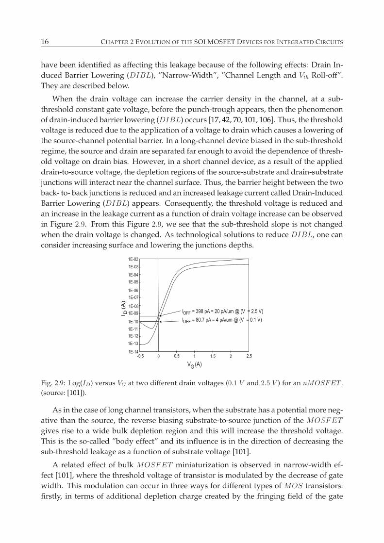
When the drain voltage can increase the carrier density in the channel, at a sub-
threshold constant gate voltage, before the punch-trough appears, then the phenomenon
of drain-induced barrier lowering (DIBL) occurs [17, 42, 70, 101, 106]. Thus, the threshold
voltage is reduced due to the application of a voltage to drain which causes a lowering of
the source-channel potential barrier. In a long-channel device biased in the sub-threshold
regime, the source and drain are separated far enough to avoid the dependence of thresh-
old voltage on drain bias. However, in a short channel device, as a result of the applied
drain-to-source voltage, the depletion regions of the source-substrate and drain-substrate
junctions will interact near the channel surface. Thus, the barrier height between the two
back- to- back junctions is reduced and an increased leakage current called Drain-Induced
Barrier Lowering (DIBL) appears. Consequently, the threshold voltage is reduced and
an increase in the leakage current as a function of drain voltage increase can be observed
in Figure 2.9. From this Figure 2.9, we see that the sub-threshold slope is not changed
when the drain voltage is changed. As technological solutions to reduce DIBL, one can
consider increasing surface and lowering the junctions depths.
Fig. 2.9: Log(ID) versus VG at two different drain voltages (0.1 V and 2.5 V ) for an nMOSFET .
(source: [101]).
As in the case of long channel transistors, when the substrate has a potential more neg-
ative than the source, the reverse biasing substrate-to-source junction of the MOSFET
gives rise to a wide bulk depletion region and this will increase the threshold voltage.
This is the so-called ”body effect” and its influence is in the direction of decreasing the
sub-threshold leakage as a function of substrate voltage [101].
A related effect of bulk MOSFET miniaturization is observed in narrow-width ef-
fect [101], where the threshold voltage of transistor is modulated by the decrease of gate
width. This modulation can occur in three ways for different types of MOS transistors:
firstly, in terms of additional depletion charge created by the fringing field of the gate
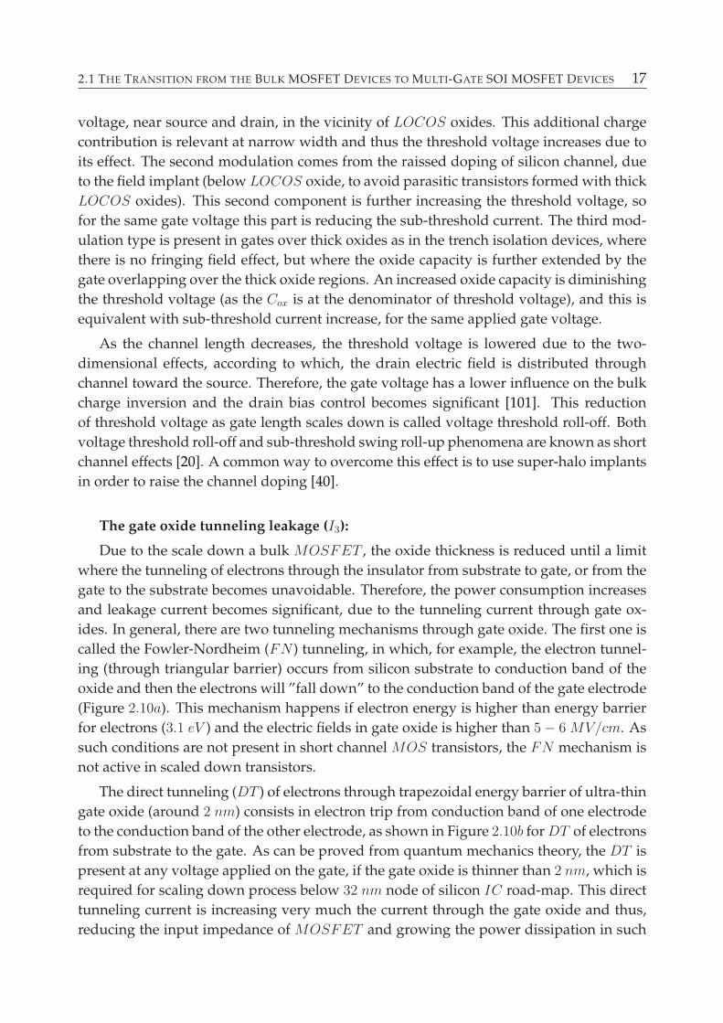
2.1 THE TRANSITION FROM THE BULK MOSFET DEVICES TO MULTI-GATE SOI MOSFET DEVICES 17
voltage, near source and drain, in the vicinity of LOCOS oxides. This additional charge
contribution is relevant at narrow width and thus the threshold voltage increases due to
its effect. The second modulation comes from the raissed doping of silicon channel, due
to the field implant (below LOCOS oxide, to avoid parasitic transistors formed with thick
LOCOS oxides). This second component is further increasing the threshold voltage, so
for the same gate voltage this part is reducing the sub-threshold current. The third mod-
ulation type is present in gates over thick oxides as in the trench isolation devices, where
there is no fringing field effect, but where the oxide capacity is further extended by the
gate overlapping over the thick oxide regions. An increased oxide capacity is diminishing
the threshold voltage (as the Cox is at the denominator of threshold voltage), and this is
equivalent with sub-threshold current increase, for the same applied gate voltage.
As the channel length decreases, the threshold voltage is lowered due to the two-
dimensional effects, according to which, the drain electric field is distributed through
channel toward the source. Therefore, the gate voltage has a lower influence on the bulk
charge inversion and the drain bias control becomes significant [101]. This reduction
of threshold voltage as gate length scales down is called voltage threshold roll-off. Both
voltage threshold roll-off and sub-threshold swing roll-up phenomena are known as short
channel effects [20]. A common way to overcome this effect is to use super-halo implants
in order to raise the channel doping [40].
The gate oxide tunneling leakage (I3):
Due to the scale down a bulk MOSFET , the oxide thickness is reduced until a limit
where the tunneling of electrons through the insulator from substrate to gate, or from the
gate to the substrate becomes unavoidable. Therefore, the power consumption increases
and leakage current becomes significant, due to the tunneling current through gate ox-
ides. In general, there are two tunneling mechanisms through gate oxide. The first one is
called the Fowler-Nordheim (FN ) tunneling, in which, for example, the electron tunnel-
ing (through triangular barrier) occurs from silicon substrate to conduction band of the
oxide and then the electrons will ”fall down” to the conduction band of the gate electrode
(Figure 2.10a). This mechanism happens if electron energy is higher than energy barrier
for electrons (3.1 eV ) and the electric fields in gate oxide is higher than 5 − 6 MV/cm. As
such conditions are not present in short channel MOS transistors, the FN mechanism is
not active in scaled down transistors.
The direct tunneling (DT ) of electrons through trapezoidal energy barrier of ultra-thin
gate oxide (around 2 nm) consists in electron trip from conduction band of one electrode
to the conduction band of the other electrode, as shown in Figure 2.10b forDT of electrons
from substrate to the gate. As can be proved from quantum mechanics theory, the DT is
present at any voltage applied on the gate, if the gate oxide is thinner than 2 nm, which is
required for scaling down process below 32 nm node of silicon IC road-map. This direct
tunneling current is increasing very much the current through the gate oxide and thus,
reducing the input impedance of MOSFET and growing the power dissipation in such
18 CHAPTER 2 EVOLUTION OF THE SOI MOSFET DEVICES FOR INTEGRATED CIRCUITS
(a) Fowler-Nordheim
tunneling of electrons.
(b) Direct tunneling of elec-
trons.
(c) Injection of hot electrons
from substrate to oxide.
Fig. 2.10: The gate oxide tunneling processes and the hot-carrier injection from substrate to oxide
(source: [101]).
MOS transistors [101, 123]. The most common solution to reduce the oxide leakage is
the replacement of SiO2 by high-k dielectric (like HfO2), which will preserve the oxide
capacitance value needed from IC design reasons (threshold voltage, speed), but they
will allow increasing the gate oxide thickness above 2 nm so that the direct tunneling is
eliminated. The equivalent oxide thickness of high-k dielectrics can be even below 2 nm,
but with physical thickness above 2 nm to avoid direct tunneling through them.
The gate current due to hot-carrier injection (I4):
The effect of hot-carrier injection refers to the semiconductor devices where, due the
high drain voltage, electrons or holes from substrate can gain enough energy (hot carri-
ers) to overcome oxide potential barrier and, then, migrate to gate [99]. The energy band
diagram of such device with high drain potential is shown in Figure 2.10c, where electron
injection to the gate is revealed. In a short-channel transistor, the electric field near the
Si/SiO2 interface is very high and provide sufficient gain for carriers to leave the sub-
strate and they enter the oxide layer. Therefore, the ”hot carriers” will generate I4 current
component and degrade the insulator causing the formation of traps and, thus, the leak-
age current appears [101].
The gate-induced drain leakage (GIDL) (I5):
GIDL current arises in silicon, below the gate, in the gate to drain overlap area due
to the gate-induced high electric field from this region. Due to zero or increased nega-
tive gate voltage, an accumulated or even an inversion region (p type), respectively, can
appear in the initial drain region, below the gate, which will change the electric field dis-
tribution in silicon, in that zone of n − MOSFET transistors. Actually, depending on
the initial drain doping level and drain voltage for an increased negative gate voltage, a
field induced p − n junction (FIJ) can appear below the gate, in the ”old” drain region,
where the electric field in the depletion area of that induced p− n junction can be so high
as to generate either band to band carrier tunneling in the field induced p − n junction
2.1 THE TRANSITION FROM THE BULK MOSFET DEVICES TO MULTI-GATE SOI MOSFET DEVICES 19
(depending on the initial doping of the n-type drain region) or carrier multiplication in
the depletion region of the FIJ . As there is a potential difference between the new born
p-type surface and the substrate, the generated holes from the surface will migrate to the
substrate. At initial low drain doping, the electric field appearing in the relatively large
depletion region of the FIJ is not high and thus, the GIDL is reduced. Similarly, if the
drain doping is very high, even if the electric field in the depletion zone of FIJ is high,
the overall volume of this depletion region is small and thus, the generated GIDL are
not considerable, which is a very good case. This is actually what happens with scaling
process (the drain and substrate doping increases). In other words, the highest GIDL
currents are generated for intermediate doping of drain, when, at high electric field in
the depletion region of FIJ , the BTBT is large enough and the carrier multiplication can
still happen. Further, these two above carrier generation mechanisms will run the GIDL
current, up to a maximum value (as the depletion area is large enough to contribute to
a relevant GIDL). Also, the thinner oxide thickness and the higher supply voltage VDD
enhance the electric field and, then, give rise to GIDL currents. In order to minimize this
effect, it is desirable to realize a very high and abrupt drain doping [16].
The channel punch-through current (I6):
Punch-through is a phenomenon that appears in the short channel devices where the
drain is very closed to the source terminal. Because of this proximity, the depletion re-
gions at the drain/substrate and source/substrate junctions extend into the channel. As
the channel length decreases, the distance between the two above-mentioned depletion
areas reduces for a constant channel doping. Therefore, a current flowing path is formed
between the drain and the source below the surface, deep in the bulk, being poorly con-
trolled by the gate terminal. Mainly, the leakage depends on the potential distribution
under the channel and drain voltage. The principal effect of the punch-through leakage
is in the sub-threshold regime through the degradation of sub-threshold slope. Thus,
it leads to an increased of power consumption [101]. The methods used to reduce the
punch-through effect are to enhance the overall substrate doping or halo implant.
In order to illustrate how the performance is influenced by the short channel effects,
Figure 2.9 shows a typical curve of drain current (ID) as a function of gate voltage (VG) in
logarithmic scale. It does worth to noticing a significant amount of drain leakage current
(IOFF ) increase due to theGIDL component, near zero VG, which increases when VD rises
and VG enhances, in absolute value. As it was mentioned above, the GIDL leakage cur-
rent is influenced by the channel doping profile, gate oxide thickness (tox), drain/source
junction depth, channel physical sizes (L,W ), threshold voltage (Vth) and bias voltage
(VDD). The DIBL current component can be also seen as a drain current increase, in the
sub-threshold region when the drain voltage grows from 0.1 V to 2.5 V . The nMOSFET
transistor from Figure 2.9 presents a current IOFF of 20 pA/µm and 4 pA/µm at the drain
voltage of 2.5 V and 0.1 V , respectively.
Over the past three decades, many improvements in circuit performance and cost per
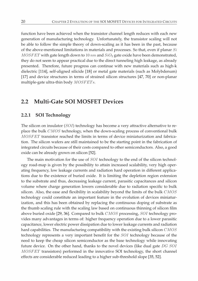
20 CHAPTER 2 EVOLUTION OF THE SOI MOSFET DEVICES FOR INTEGRATED CIRCUITS
function have been achieved when the transistor channel length reduces with each new
generation of manufacturing technology. Unfortunately, the transistor scaling will not
be able to follow the simple theory of down-scaling as it has been in the past, because
of the above-mentioned limitations in materials and processes. So that, even if planar Si
MOSFET with gate length down to 10 nm and SiO2 gate oxide have been demonstrated,
they do not seem to appear practical due to the direct tunneling high leakage, as already
presented. Therefore, future progress can continue with new materials such as high-k
dielectric [114], self-aligned silicide [18] or metal gate materials (such as Molybdenum)
[17] and device structures in terms of strained silicon structures [47, 70] or non-planar
multiple-gate ultra-thin body MOSFETs.
2.2 Multi-Gate SOI MOSFET Devices
2.2.1 SOI Technology
The silicon on insulator (SOI) technology has become a very attractive alternative to re-
place the bulk CMOS technology, when the down-scaling process of conventional bulk
MOSFET transistor reached the limits in terms of device miniaturization and fabrica-
tion. The silicon wafers are still maintained to be the starting point in the fabrication of
integrated circuits because of their costs compared to other semiconductors. Also, a good
oxide can be already grown on silicon [52].
The main motivation for the use of SOI technology to the end of the silicon technol-
ogy road-map is given by the possibility to attain increased scalability, very high oper-
ating frequency, low leakage currents and radiation hard operation in different applica-
tions due to the existence of buried oxide. It is limiting the depletion region extension
to the substrate and thus, decreasing leakage current, parasitic capacitances and silicon
volume where charge generation lowers considerable due to radiation specific to bulk
silicon. Also, the ease and flexibility in scalability beyond the limits of the bulk CMOS
technology could constitute an important feature in the evolution of devices miniatur-
ization, and this has been obtained by replacing the continuous doping of substrate as
the thumb scaling rule with the scaling law based on continuous thinning of silicon film
above buried oxide [29, 36]. Compared to bulk CMOS processing, SOI technology pro-
vides many advantages in terms of: higher frequency operation due to a lower parasitic
capacitance, lower electric power dissipation due to lower leakage currents and radiation
hard capabilities. The manufacturing compatibility with the existing bulk silicon CMOS
technology represents a very important benefit for the SOI technology because of the
need to keep the cheap silicon semiconductor as the base technology while innovating
future device. On the other hand, thanks to the novel devices (like dual gate DG SOI
MOSFET transistors) performed in the innovative SOI technology, the short channel
effects are considerable reduced leading to a higher sub-threshold slope [35, 52].
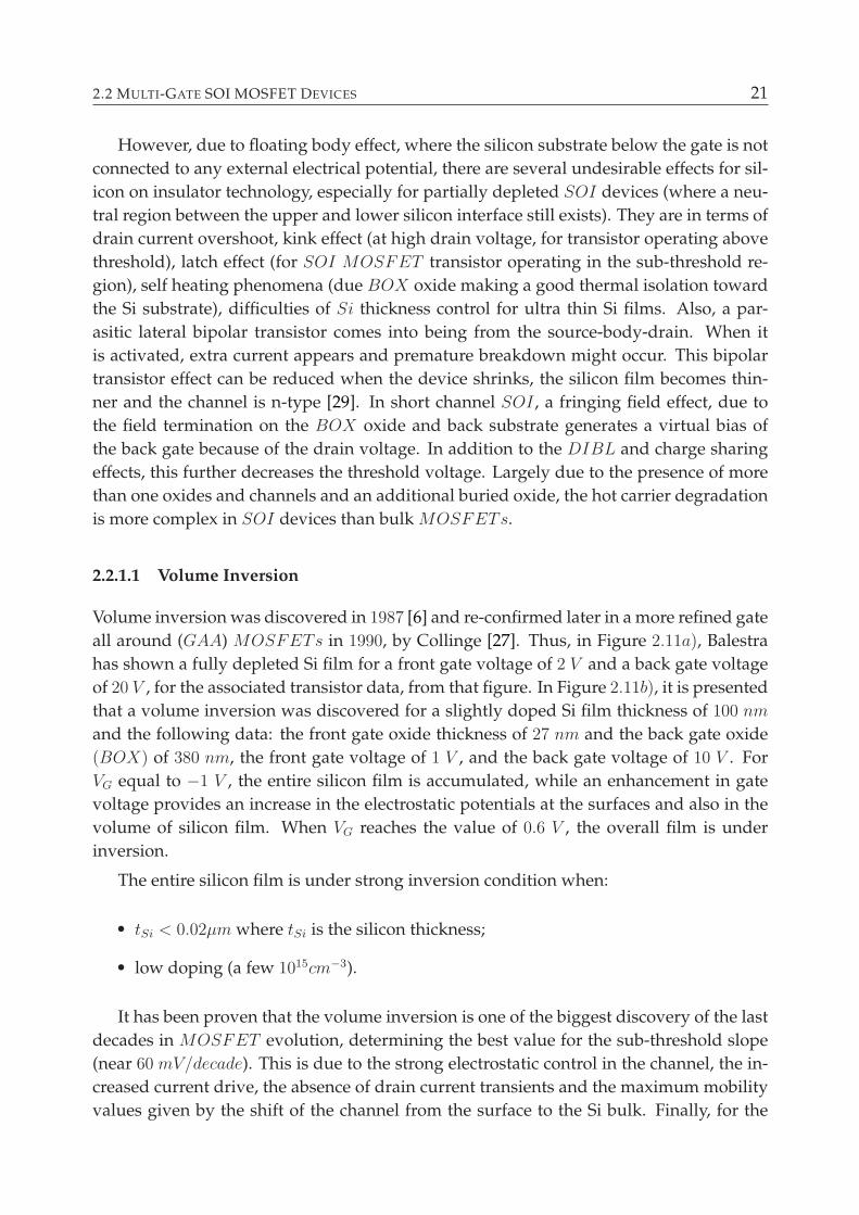
2.2 MULTI-GATE SOI MOSFET DEVICES 21
However, due to floating body effect, where the silicon substrate below the gate is not
connected to any external electrical potential, there are several undesirable effects for sil-
icon on insulator technology, especially for partially depleted SOI devices (where a neu-
tral region between the upper and lower silicon interface still exists). They are in terms of
drain current overshoot, kink effect (at high drain voltage, for transistor operating above
threshold), latch effect (for SOI MOSFET transistor operating in the sub-threshold re-
gion), self heating phenomena (due BOX oxide making a good thermal isolation toward
the Si substrate), difficulties of Si thickness control for ultra thin Si films. Also, a par-
asitic lateral bipolar transistor comes into being from the source-body-drain. When it
is activated, extra current appears and premature breakdown might occur. This bipolar
transistor effect can be reduced when the device shrinks, the silicon film becomes thin-
ner and the channel is n-type [29]. In short channel SOI , a fringing field effect, due to
the field termination on the BOX oxide and back substrate generates a virtual bias of
the back gate because of the drain voltage. In addition to the DIBL and charge sharing
effects, this further decreases the threshold voltage. Largely due to the presence of more
than one oxides and channels and an additional buried oxide, the hot carrier degradation
is more complex in SOI devices than bulk MOSFETs.
2.2.1.1 Volume Inversion
Volume inversion was discovered in 1987 [6] and re-confirmed later in a more refined gate
all around (GAA) MOSFETs in 1990, by Collinge [27]. Thus, in Figure 2.11a), Balestra
has shown a fully depleted Si film for a front gate voltage of 2 V and a back gate voltage
of 20 V , for the associated transistor data, from that figure. In Figure 2.11b), it is presented
that a volume inversion was discovered for a slightly doped Si film thickness of 100 nm
and the following data: the front gate oxide thickness of 27 nm and the back gate oxide
(BOX) of 380 nm, the front gate voltage of 1 V , and the back gate voltage of 10 V . For
VG equal to −1 V , the entire silicon film is accumulated, while an enhancement in gate
voltage provides an increase in the electrostatic potentials at the surfaces and also in the
volume of silicon film. When VG reaches the value of 0.6 V , the overall film is under
inversion.
The entire silicon film is under strong inversion condition when:
• tSi < 0.02µm where tSi is the silicon thickness;
• low doping (a few 1015cm−3).
It has been proven that the volume inversion is one of the biggest discovery of the last
decades in MOSFET evolution, determining the best value for the sub-threshold slope
(near 60 mV/decade). This is due to the strong electrostatic control in the channel, the in-
creased current drive, the absence of drain current transients and the maximum mobility
values given by the shift of the channel from the surface to the Si bulk. Finally, for the
22 CHAPTER 2 EVOLUTION OF THE SOI MOSFET DEVICES FOR INTEGRATED CIRCUITS
aaaa
Fig. 2.11: Potential Profile inside the Silicon Film for (a) un-coupling interfaces (doping NA =
4 · 1016 cm−3, film thickness tSi = 300 nm) and (b) coupling interfaces (NA = 3 · 1015 cm−3,
tSi = 100 nm). x is the distance from the front interface (source: [6]).
minimum thickness of Si film below 5 nm, a maximum transconductance is obtained in
the range of impacts on carrier profile in the film, providing an indirect improvement of
the effective mobility [36]. Thus, the current drive capability and outstanding transcon-
ductance gain are raised.
2.2.2 SOI MOSFET Devices
SOI MOSFET devices can be classified as a function of the thickness of silicon layer into
two big classes: partially-depleted (PD) and fully-depleted (FD) SOI MOSFETs. They
are going to be described further.
2.2.2.1 Partially Depleted SOI MOSFET
Figure 2.12 shows a partially depleted silicon on insulator MOSFET device. It is defined
as aMOSFET transistor realized with SOI technology and in which the depletion region
does not extend in the whole silicon film of SOI and therefore, a neutral region of the Si
layer will survive, even after biasing the device in the inversion inversion. Thus, the
silicon film thickness is greater than the maximum gate depletion width. The neutral
region of silicon is called ”body”.
In partially depleted SOI MOSFETs, if the body of the transistor is not connected
to an external potential, then the floating body effects appear. One of these is the ”kink
effects” arising at high drain to source voltage due to the majority carriers generated by
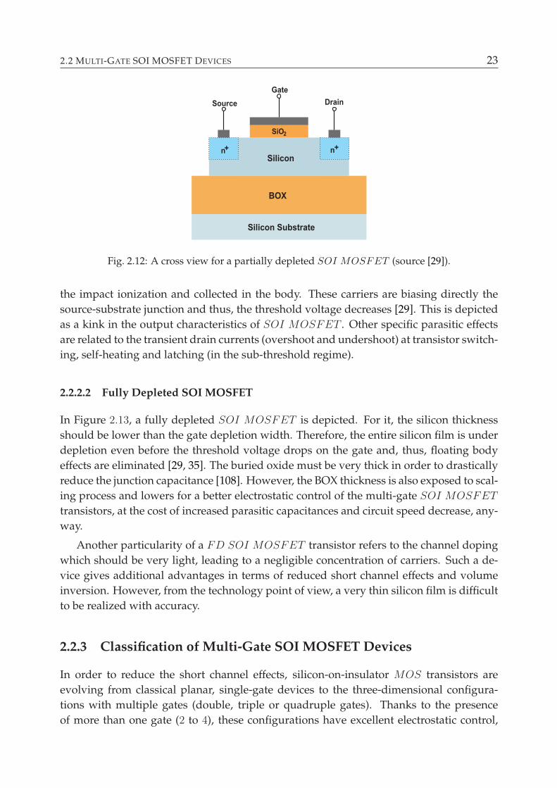
2.2 MULTI-GATE SOI MOSFET DEVICES 23
Fig. 2.12: A cross view for a partially depleted SOI MOSFET (source [29]).
the impact ionization and collected in the body. These carriers are biasing directly the
source-substrate junction and thus, the threshold voltage decreases [29]. This is depicted
as a kink in the output characteristics of SOI MOSFET . Other specific parasitic effects
are related to the transient drain currents (overshoot and undershoot) at transistor switch-
ing, self-heating and latching (in the sub-threshold regime).
2.2.2.2 Fully Depleted SOI MOSFET
In Figure 2.13, a fully depleted SOI MOSFET is depicted. For it, the silicon thickness
should be lower than the gate depletion width. Therefore, the entire silicon film is under
depletion even before the threshold voltage drops on the gate and, thus, floating body
effects are eliminated [29, 35]. The buried oxide must be very thick in order to drastically
reduce the junction capacitance [108]. However, the BOX thickness is also exposed to scal-
ing process and lowers for a better electrostatic control of the multi-gate SOI MOSFET
transistors, at the cost of increased parasitic capacitances and circuit speed decrease, any-
way.
Another particularity of a FD SOI MOSFET transistor refers to the channel doping
which should be very light, leading to a negligible concentration of carriers. Such a de-
vice gives additional advantages in terms of reduced short channel effects and volume
inversion. However, from the technology point of view, a very thin silicon film is difficult
to be realized with accuracy.
2.2.3 Classification of Multi-Gate SOI MOSFET Devices
In order to reduce the short channel effects, silicon-on-insulator MOS transistors are
evolving from classical planar, single-gate devices to the three-dimensional configura-
tions with multiple gates (double, triple or quadruple gates). Thanks to the presence
of more than one gate (2 to 4), these configurations have excellent electrostatic control,
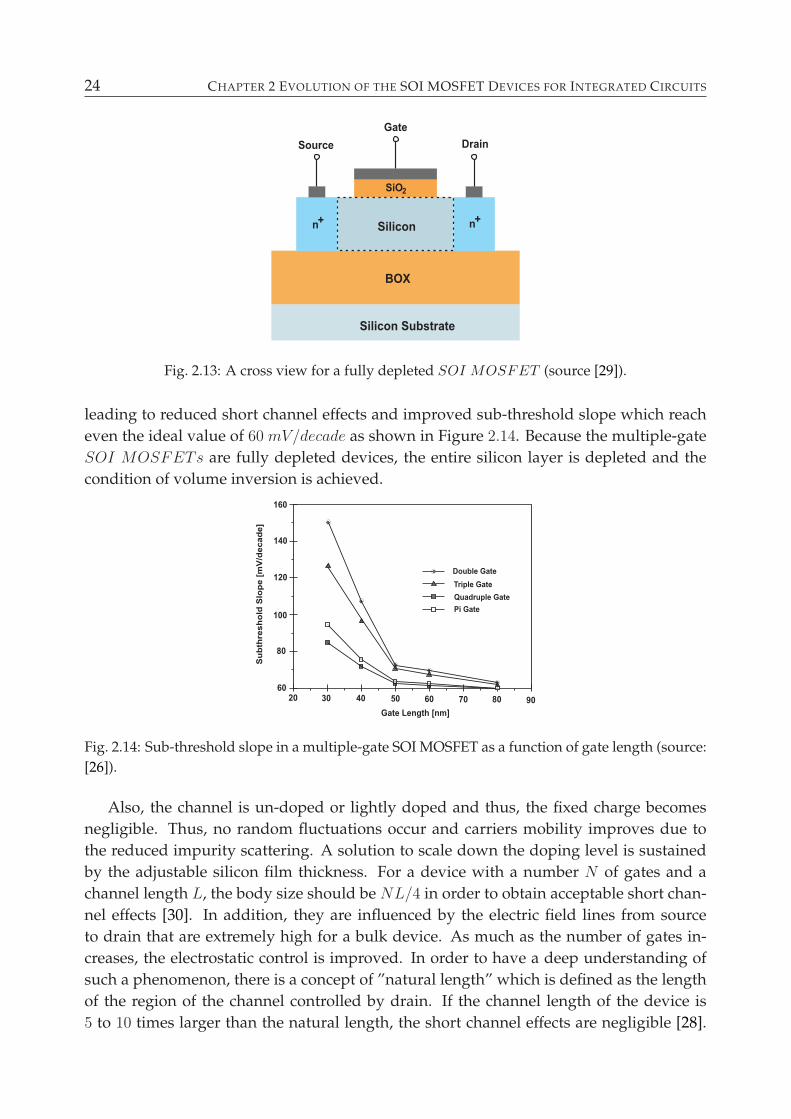
24 CHAPTER 2 EVOLUTION OF THE SOI MOSFET DEVICES FOR INTEGRATED CIRCUITS
Fig. 2.13: A cross view for a fully depleted SOI MOSFET (source [29]).
leading to reduced short channel effects and improved sub-threshold slope which reach
even the ideal value of 60 mV/decade as shown in Figure 2.14. Because the multiple-gate
SOI MOSFETs are fully depleted devices, the entire silicon layer is depleted and the
condition of volume inversion is achieved.
Fig. 2.14: Sub-threshold slope in a multiple-gate SOI MOSFET as a function of gate length (source:
[26]).
Also, the channel is un-doped or lightly doped and thus, the fixed charge becomes
negligible. Thus, no random fluctuations occur and carriers mobility improves due to
the reduced impurity scattering. A solution to scale down the doping level is sustained
by the adjustable silicon film thickness. For a device with a number N of gates and a
channel length L, the body size should be NL/4 in order to obtain acceptable short chan-
nel effects [30]. In addition, they are influenced by the electric field lines from source
to drain that are extremely high for a bulk device. As much as the number of gates in-
creases, the electrostatic control is improved. In order to have a deep understanding of
such a phenomenon, there is a concept of ”natural length” which is defined as the length
of the region of the channel controlled by drain. If the channel length of the device is
5 to 10 times larger than the natural length, the short channel effects are negligible [28].
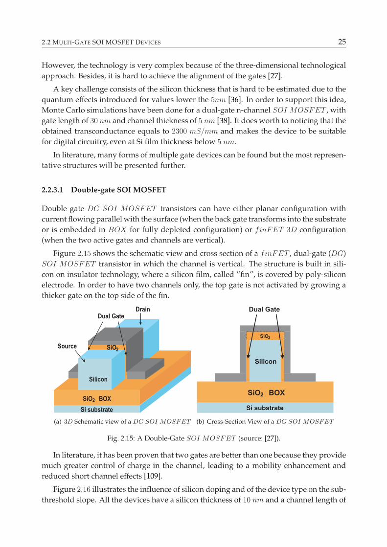
2.2 MULTI-GATE SOI MOSFET DEVICES 25
However, the technology is very complex because of the three-dimensional technological
approach. Besides, it is hard to achieve the alignment of the gates [27].
A key challenge consists of the silicon thickness that is hard to be estimated due to the
quantum effects introduced for values lower the 5nm [36]. In order to support this idea,
Monte Carlo simulations have been done for a dual-gate n-channel SOI MOSFET , with
gate length of 30 nm and channel thickness of 5 nm [38]. It does worth to noticing that the
obtained transconductance equals to 2300 mS/mm and makes the device to be suitable
for digital circuitry, even at Si film thickness below 5 nm.
In literature, many forms of multiple gate devices can be found but the most represen-
tative structures will be presented further.
2.2.3.1 Double-gate SOI MOSFET
Double gate DG SOI MOSFET transistors can have either planar configuration with
current flowing parallel with the surface (when the back gate transforms into the substrate
or is embedded in BOX for fully depleted configuration) or finFET 3D configuration
(when the two active gates and channels are vertical).
Figure 2.15 shows the schematic view and cross section of a finFET , dual-gate (DG)
SOI MOSFET transistor in which the channel is vertical. The structure is built in sili-
con on insulator technology, where a silicon film, called ”fin”, is covered by poly-silicon
electrode. In order to have two channels only, the top gate is not activated by growing a
thicker gate on the top side of the fin.
(a) 3D Schematic view of a DG SOI MOSFET (b) Cross-Section View of a DG SOI MOSFET
Fig. 2.15: A Double-Gate SOI MOSFET (source: [27]).
In literature, it has been proven that two gates are better than one because they provide
much greater control of charge in the channel, leading to a mobility enhancement and
reduced short channel effects [109].
Figure 2.16 illustrates the influence of silicon doping and of the device type on the sub-
threshold slope. All the devices have a silicon thickness of 10 nm and a channel length of
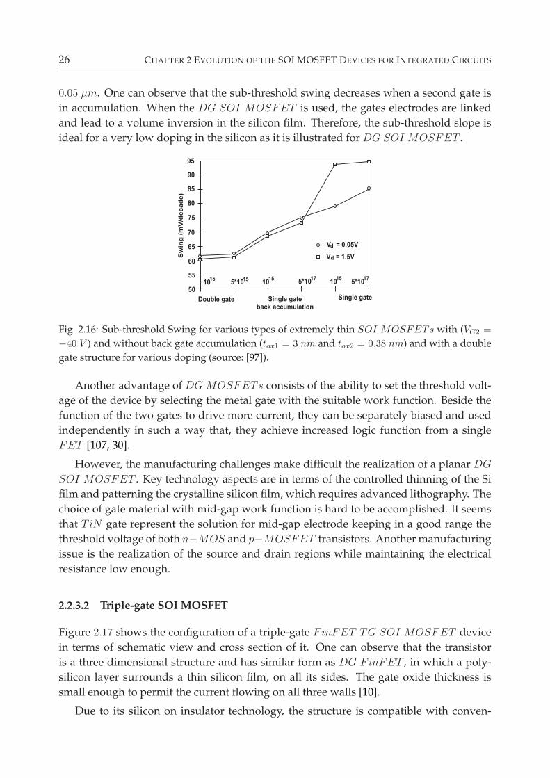
26 CHAPTER 2 EVOLUTION OF THE SOI MOSFET DEVICES FOR INTEGRATED CIRCUITS
0.05 µm. One can observe that the sub-threshold swing decreases when a second gate is
in accumulation. When the DG SOI MOSFET is used, the gates electrodes are linked
and lead to a volume inversion in the silicon film. Therefore, the sub-threshold slope is
ideal for a very low doping in the silicon as it is illustrated for DG SOI MOSFET .
Fig. 2.16: Sub-threshold Swing for various types of extremely thin SOI MOSFETs with (VG2 =
−40 V ) and without back gate accumulation (tox1 = 3 nm and tox2 = 0.38 nm) and with a double
gate structure for various doping (source: [97]).
Another advantage of DGMOSFETs consists of the ability to set the threshold volt-
age of the device by selecting the metal gate with the suitable work function. Beside the
function of the two gates to drive more current, they can be separately biased and used
independently in such a way that, they achieve increased logic function from a single
FET [107, 30].
However, the manufacturing challenges make difficult the realization of a planar DG
SOI MOSFET . Key technology aspects are in terms of the controlled thinning of the Si
film and patterning the crystalline silicon film, which requires advanced lithography. The
choice of gate material with mid-gap work function is hard to be accomplished. It seems
that TiN gate represent the solution for mid-gap electrode keeping in a good range the
threshold voltage of both n−MOS and p−MOSFET transistors. Another manufacturing
issue is the realization of the source and drain regions while maintaining the electrical
resistance low enough.
2.2.3.2 Triple-gate SOI MOSFET
Figure 2.17 shows the configuration of a triple-gate FinFET TG SOI MOSFET device
in terms of schematic view and cross section of it. One can observe that the transistor
is a three dimensional structure and has similar form as DG FinFET , in which a poly-
silicon layer surrounds a thin silicon film, on all its sides. The gate oxide thickness is
small enough to permit the current flowing on all three walls [10].
Due to its silicon on insulator technology, the structure is compatible with conven-
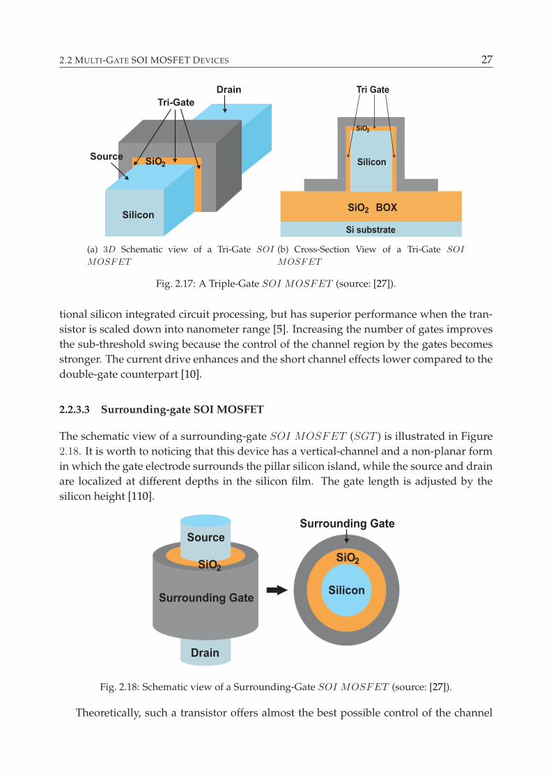
2.2 MULTI-GATE SOI MOSFET DEVICES 27
(a) 3D Schematic view of a Tri-Gate SOI
MOSFET
(b) Cross-Section View of a Tri-Gate SOI
MOSFET
Fig. 2.17: A Triple-Gate SOI MOSFET (source: [27]).
tional silicon integrated circuit processing, but has superior performance when the tran-
sistor is scaled down into nanometer range [5]. Increasing the number of gates improves
the sub-threshold swing because the control of the channel region by the gates becomes
stronger. The current drive enhances and the short channel effects lower compared to the
double-gate counterpart [10].
2.2.3.3 Surrounding-gate SOI MOSFET
The schematic view of a surrounding-gate SOI MOSFET (SGT ) is illustrated in Figure
2.18. It is worth to noticing that this device has a vertical-channel and a non-planar form
in which the gate electrode surrounds the pillar silicon island, while the source and drain
are localized at different depths in the silicon film. The gate length is adjusted by the
silicon height [110].
Fig. 2.18: Schematic view of a Surrounding-Gate SOI MOSFET (source: [27]).
Theoretically, such a transistor offers almost the best possible control of the channel
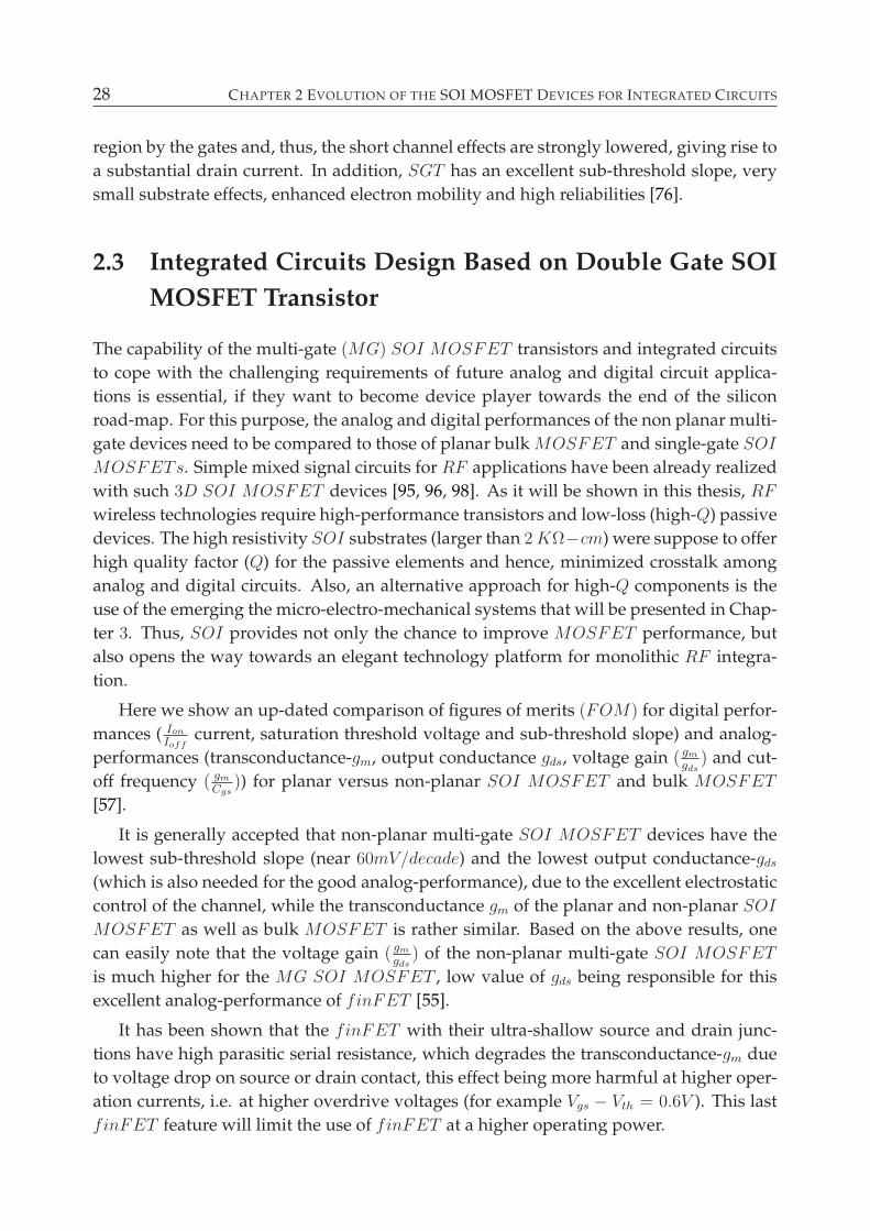
28 CHAPTER 2 EVOLUTION OF THE SOI MOSFET DEVICES FOR INTEGRATED CIRCUITS
region by the gates and, thus, the short channel effects are strongly lowered, giving rise to
a substantial drain current. In addition, SGT has an excellent sub-threshold slope, very
small substrate effects, enhanced electron mobility and high reliabilities [76].
2.3 Integrated Circuits Design Based on Double Gate SOI
MOSFET Transistor
The capability of the multi-gate (MG) SOI MOSFET transistors and integrated circuits
to cope with the challenging requirements of future analog and digital circuit applica-
tions is essential, if they want to become device player towards the end of the silicon
road-map. For this purpose, the analog and digital performances of the non planar multi-
gate devices need to be compared to those of planar bulk MOSFET and single-gate SOI
MOSFETs. Simple mixed signal circuits for RF applications have been already realized
with such 3D SOI MOSFET devices [95, 96, 98]. As it will be shown in this thesis, RF
wireless technologies require high-performance transistors and low-loss (high-Q) passive
devices. The high resistivity SOI substrates (larger than 2KΩ−cm) were suppose to offer
high quality factor (Q) for the passive elements and hence, minimized crosstalk among
analog and digital circuits. Also, an alternative approach for high-Q components is the
use of the emerging the micro-electro-mechanical systems that will be presented in Chap-
ter 3. Thus, SOI provides not only the chance to improve MOSFET performance, but
also opens the way towards an elegant technology platform for monolithic RF integra-
tion.
Here we show an up-dated comparison of figures of merits (FOM) for digital perfor-
mances ( IonIoff
current, saturation threshold voltage and sub-threshold slope) and analog-
performances (transconductance-gm, output conductance gds, voltage gain ( gmgds
) and cut-
off frequency ( gmCgs
)) for planar versus non-planar SOI MOSFET and bulk MOSFET
[57].
It is generally accepted that non-planar multi-gate SOI MOSFET devices have the
lowest sub-threshold slope (near 60mV/decade) and the lowest output conductance-gds
(which is also needed for the good analog-performance), due to the excellent electrostatic
control of the channel, while the transconductance gm of the planar and non-planar SOI
MOSFET as well as bulk MOSFET is rather similar. Based on the above results, one
can easily note that the voltage gain ( gmgds
) of the non-planar multi-gate SOI MOSFET
is much higher for the MG SOI MOSFET , low value of gds being responsible for this
excellent analog-performance of finFET [55].
It has been shown that the finFET with their ultra-shallow source and drain junc-
tions have high parasitic serial resistance, which degrades the transconductance-gm due
to voltage drop on source or drain contact, this effect being more harmful at higher oper-
ation currents, i.e. at higher overdrive voltages (for example Vgs − Vth = 0.6V ). This last
finFET feature will limit the use of finFET at a higher operating power.
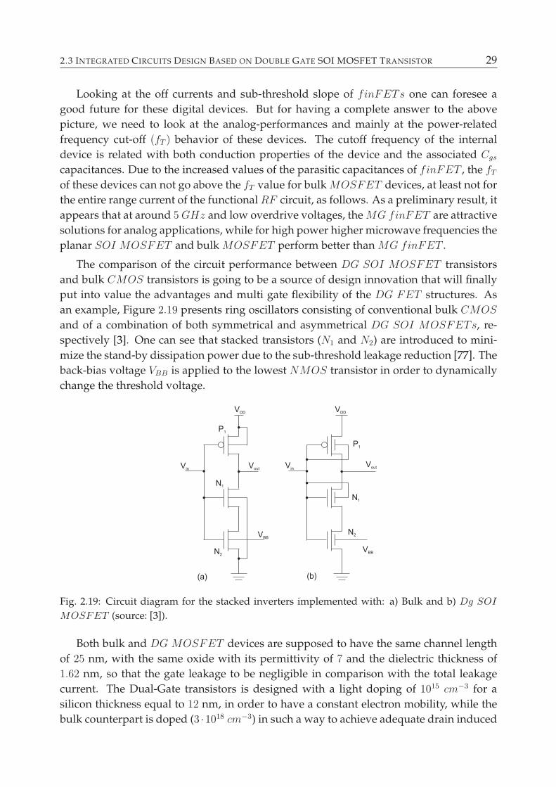
2.3 INTEGRATED CIRCUITS DESIGN BASED ON DOUBLE GATE SOI MOSFET TRANSISTOR 29
Looking at the off currents and sub-threshold slope of finFETs one can foresee a
good future for these digital devices. But for having a complete answer to the above
picture, we need to look at the analog-performances and mainly at the power-related
frequency cut-off (fT ) behavior of these devices. The cutoff frequency of the internal
device is related with both conduction properties of the device and the associated Cgs
capacitances. Due to the increased values of the parasitic capacitances of finFET , the fT
of these devices can not go above the fT value for bulk MOSFET devices, at least not for
the entire range current of the functional RF circuit, as follows. As a preliminary result, it
appears that at around 5GHz and low overdrive voltages, theMG finFET are attractive
solutions for analog applications, while for high power higher microwave frequencies the
planar SOI MOSFET and bulk MOSFET perform better than MG finFET .
The comparison of the circuit performance between DG SOI MOSFET transistors
and bulk CMOS transistors is going to be a source of design innovation that will finally
put into value the advantages and multi gate flexibility of the DG FET structures. As
an example, Figure 2.19 presents ring oscillators consisting of conventional bulk CMOS
and of a combination of both symmetrical and asymmetrical DG SOI MOSFETs, re-
spectively [3]. One can see that stacked transistors (N1 and N2) are introduced to mini-
mize the stand-by dissipation power due to the sub-threshold leakage reduction [77]. The
back-bias voltage VBB is applied to the lowest NMOS transistor in order to dynamically
change the threshold voltage.
Fig. 2.19: Circuit diagram for the stacked inverters implemented with: a) Bulk and b) Dg SOI
MOSFET (source: [3]).
Both bulk and DG MOSFET devices are supposed to have the same channel length
of 25 nm, with the same oxide with its permittivity of 7 and the dielectric thickness of
1.62 nm, so that the gate leakage to be negligible in comparison with the total leakage
current. The Dual-Gate transistors is designed with a light doping of 1015 cm−3 for a
silicon thickness equal to 12 nm, in order to have a constant electron mobility, while the
bulk counterpart is doped (3 ·1018 cm−3) in such a way to achieve adequate drain induced
30 CHAPTER 2 EVOLUTION OF THE SOI MOSFET DEVICES FOR INTEGRATED CIRCUITS
barrier leakage and sub-threshold slope.
The simulations results indicate that the DG SOI MOSFETs are consuming less
power with respect to bulk MOSFETs due to their stronger leakage suppression shown
by the smaller sub-threshold slope for the SOI devices (78.9 mV/dec) compared to that
of conventional MOSFETs (89.1 mV/dec) (see Figure 2.20) [3]. This advantage is mainly
provided by the threshold voltage sensitivity to the bias voltage VBB. It has been also
proven that the energy overhead of SOI circuits due to the switching from active to
stand-by mode is decreased by more than one order of magnitude, as compared to bulk
devices [3].
Fig. 2.20: Dependence of the leakage current reduction factor due to transistor stacking Istack/Idev
on back-bias voltage VBB (source: [3]).
This proven ability of the SOI devices to integrate both low power and high perfor-
manceRF on the same platform has opened a variety of interesting areas to explore, such
as the communication and the mixed-circuit applications [100]. This is only the beginning
and the challenge of intensive analyses in the field for future innovative solutions operat-
ing in the range of 40 − 60 GHz wireless applications.
2.4 Summary
The purpose of the current chapter is to offer a short description of the evolution of
MOSFET devices, by making the transition from silicon bulk technology to the silicon-
on-insulator technology, with its volume inversion capability. Thus, the chapter begins
with the history of electron devices starting from the discovery of the unipolar and bipo-
lar and ending with the present devices. According to Moore’s law, the scaling rules were
described and then, several road-maps showed how their applicability was possible to the
device miniaturization. The short channel effects, the limits and leakage currents resulted
from scaling process have been illustrated in this chapter. Afterwards, the silicon-on-
2.4 SUMMARY 31
insulator evolution was described by presenting the most important multi gate devices
made with this technology. The integrated circuit based on double-gate, triple and Gate
All Around SOI MOSFET devices silicon on insulatorMOSFET transistor were briefly
included.
The progress was very well predicted by Moore’s law who envisioned that dimen-
sions will decrease on an exponential curve with number of transistors doubling every
two years. This scaling journey went on in the last four decades reaching the current
integrated circuits state of art with more than a billion transistors and a channel length
lower than 14 nm by 2020. The need of smaller and high efficiency chips has led to the ex-
ploration of nanometer scale CMOS alternatives, such as multiple-gate SOI MOSFET
devices.
The continuous process of down-scaling has reached its limits in terms of gate oxide
thickness, short channel effects and power consumptions. This evolution gave birth to
new leakage mechanisms described in this chapter and, accordingly solutions needed to
overcome them. Therefore, the silicon on insulator devices were supposed to replace the
bulk MOSFET transistors. This chapter includes the advantages and challenges for the
multi-gate SOI MOSFET devices, together with their possible analog applications.

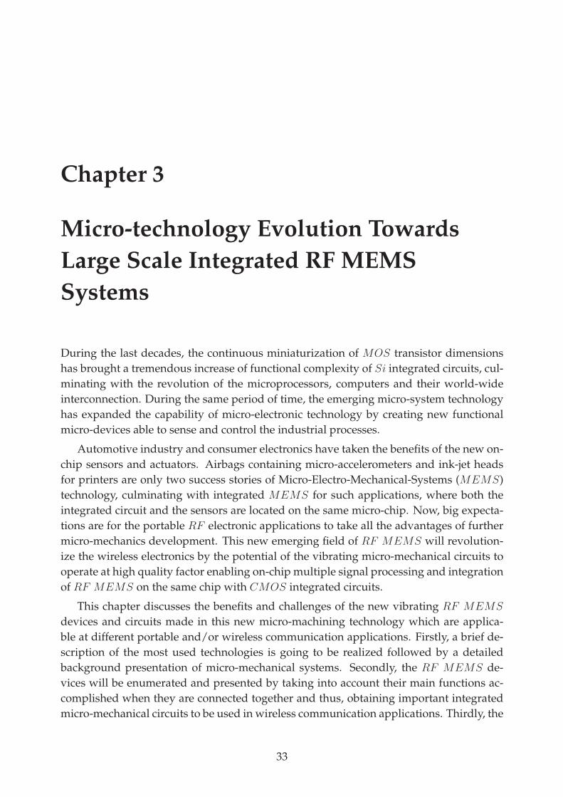
Chapter 3
Micro-technology Evolution Towards
Large Scale Integrated RF MEMS
Systems
During the last decades, the continuous miniaturization of MOS transistor dimensions
has brought a tremendous increase of functional complexity of Si integrated circuits, cul-
minating with the revolution of the microprocessors, computers and their world-wide
interconnection. During the same period of time, the emerging micro-system technology
has expanded the capability of micro-electronic technology by creating new functional
micro-devices able to sense and control the industrial processes.
Automotive industry and consumer electronics have taken the benefits of the new on-
chip sensors and actuators. Airbags containing micro-accelerometers and ink-jet heads
for printers are only two success stories of Micro-Electro-Mechanical-Systems (MEMS)
technology, culminating with integrated MEMS for such applications, where both the
integrated circuit and the sensors are located on the same micro-chip. Now, big expecta-
tions are for the portable RF electronic applications to take all the advantages of further
micro-mechanics development. This new emerging field of RF MEMS will revolution-
ize the wireless electronics by the potential of the vibrating micro-mechanical circuits to
operate at high quality factor enabling on-chip multiple signal processing and integration
of RF MEMS on the same chip with CMOS integrated circuits.
This chapter discusses the benefits and challenges of the new vibrating RF MEMS
devices and circuits made in this new micro-machining technology which are applica-
ble at different portable and/or wireless communication applications. Firstly, a brief de-
scription of the most used technologies is going to be realized followed by a detailed
background presentation of micro-mechanical systems. Secondly, the RF MEMS de-
vices will be enumerated and presented by taking into account their main functions ac-
complished when they are connected together and thus, obtaining important integrated
micro-mechanical circuits to be used in wireless communication applications. Thirdly, the
33
34CHAPTER 3 MICRO-TECHNOLOGY EVOLUTION TOWARDS LARGE SCALE INTEGRATED RF MEMS
SYSTEMS
evolution of transceiver architectures will be presented, starting from the present gener-
ation where CMOS integrated circuits interface at the board level with off-chip quartz-
based passive components for getting transceiver architectures, performed on printed
circuit board (PCB) and ending up with an ultimate vision of an all-MEMS transceiver,
in which all the above-mentioned off chip elements are performed in the silicon MEMS
technology and located on a single silicon chip. In the end, several challenges concern-
ing the on-going RF vibrating MEMS research will be discussed and a summary will
conclude the chapter.
3.1 MEMS Technology
There are several MEMS micro fabrication technologies discussed over the last years.
These technologies offer the possibility to construct both mechanical and electrical com-
ponents with sizes down to micron and even below. Their number on the chip is contin-
uously increasing.
Independent on the classification of MEMS technologies, there are several common
properties as: miniaturization, multiplicity and integrability [7, 41].
Basically, miniaturization refers to size minimization of MEMS components and this
conveys several advantages. As a result of size reduction, the natural resonant frequency
increases and, further, the system operating frequencies. Also, the thermal time constant
is shorter. However, the miniaturization is done until an operational and technological
limit is reached and that is different from one application to another. The second im-
portant property, called multiplicity, has two benefits in terms of: 1) the possibility to
fabricate 10000 or a million components at the same time as one component and 2) the
additional flexibility in the realization of parallel interconnected electromechanical sys-
tems. The previous characteristics are not enough exploited if the microelectronics is not
merged with the micro-mechanics and, thus, reaching the integrated MEMS systems.
The most common processing techniques that are used to construct micro-mechanical
structures are bulk and surface micro-machining [71, 74, 116].
3.1.1 Bulk Micro-machining
The bulk micro-machining [56, 74] is defined as a technology that makes micro-structures,
in which the bulk silicon material is chemically etched. The etching properties are strongly
dependent on the crystallographic structure of the semiconductor bulk material.
3.2 NEED FOR A MICRO-MECHANICAL CIRCUIT TECHNOLOGY 35
Fig. 3.1: Micro-machining technology: bulk and surface [37].
3.1.2 Surface Micro-machining
Another predominant micro-machining technology is the so-called surface micro-machining
[74]. It starts with a silicon wafer which is, in this case, the silicon substrate. Then, in-
stead of etching the bulk silicon, a thin ”sacrificial layer” is removed from underneath the
mechanical structure with the scope of suspending it from the substrate.
The surface micro-machining enables the fabrication of very complex micro-structures
and makes realizable the constructions of systems that are impossible to be built with bulk
or conventional technology. In addition, it offers the freedom for an easier fabrication of
the integrated MEMS with minimum compromises in materials, geometries, assembly
and interconnections.
3.2 Need for a Micro-mechanical Circuit Technology
The MEMS devices are seen as elements with new capabilities, extended operational
performances and lifetimes of existing mechanical systems. In addition, there are many
possibilities for MEMS to be used in applications such as accelerometers, ink-jet print
heads, hearing aids, pressure and chemical sensors, infrared imagers, gyroscopes, digital
light processors, radio frequency and optical wireless communication [15, 41].
Today, the main motivation of the use of MEMS technology is the miniaturization of
the RF Front Ends in wireless applications. For this purpose, an ultra high quality factor
(over 10000) is a paramount need of MEMS usage in order to provide good selective
low-loss filters and/or high-accuracy voltage controlled oscillators. Moreover, surface
micro-machined MEMS can be interpreted as a fabrication approach that provides the
advantages of multiplicity (batch fabrication), easier monolithic fabrication with the elec-
tronics on the same chip, miniaturization (micro-scale sizes and low mass of devices)
36CHAPTER 3 MICRO-TECHNOLOGY EVOLUTION TOWARDS LARGE SCALE INTEGRATED RF MEMS
SYSTEMS
and high reliability. On the other hand, there are a few challenges to consider: the com-
patibility of structural MEMS technology with the CMOS IC process, the fabrication
approach, cost, time and packaging.
3.3 MEMS Systems - Present and Perspectives
Recently, MEMS is extending the application range from physico-chemical sensing to
signal processing by exploiting the high quality factor of the vibrating micro-structures
operating at the natural resonance frequency. The MEMS capability to perform new
functions in the field of wireless electronic application will revolutionize the next gen-
eration of communication industry. Actually, the RF integrated mechanical circuits are
envisioned to grow in complexity, from low scale to medium scale and large scale inte-
grated MEMS in a similar way the integrated circuit have developed in the years ′60
- ′90 of the previous century. This extraordinary evolution is only possible if the basic
science and technology of MEMS is deeply understood and applied in market applica-
tions, at low cost and high reliability. To reach this final goal, the MEMS community is
trying to use the basic physics and electronics knowledge for supporting the new emerg-
ing applications of RF MEMS devices and circuits (see Appendix A for a background
presentation of time and frequency response of systems of different orders). Intensive
research around vibrating RF MEMS capacitive structures have shown that if these RF -
MEMS vibrating components are excited with an ac electrical signal of frequency equal
to the natural mechanical resonant frequency, they can have equivalent electric circuits
made of R, L, C passive components having the advantage of high quality factors, which
make them very attractive for RF applications. These silicon RF MEMS structures can
be technologically integrated on the same chip with CMOS electronics for getting a low
size high performance integrated oscillator, and this aspect makes them a real threat to
the quartz resonators used in the V CO oscillators.
Actually, such a trend of replacing quartz resonators by siliconRF MEMS resonators
is already happening today. For example a micro-electro-mechanical system (MEMS)
oscillator (SiT8002) has been introduced by Discera company, in August of 2007. Such
a highly reliable oscillator is completely quartz free and works in the frequency range
from 1 MHz up to 125 MHz, with an excellent temperature and jitter performance. The
SiT8002 is a factory programmable device at the customer’s frequency specifications and
can be used in several applications such as digital video recorder, IP -phone, scanner, IP
camera [1] and this is only the beginning of a long and successful journey of RF MEMS
micro-nano structures envisaged for future RF electronics applications.
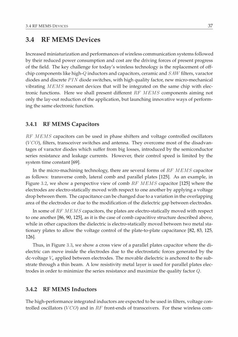
3.4 RF MEMS DEVICES 37
3.4 RF MEMS Devices
Increased miniaturization and performances of wireless communication systems followed
by their reduced power consumption and cost are the driving forces of present progress
of the field. The key challenge for today’s wireless technology is the replacement of off-
chip components like high-Q inductors and capacitors, ceramic and SAW filters, varactor
diodes and discrete PIN diode switches, with high quality factor, new micro-mechanical
vibrating MEMS resonant devices that will be integrated on the same chip with elec-
tronic functions. Here we shall present different RF MEMS components aiming not
only the lay-out reduction of the application, but launching innovative ways of perform-
ing the same electronic function.
3.4.1 RF MEMS Capacitors
RF MEMS capacitors can be used in phase shifters and voltage controlled oscillators
(V CO), filters, transceiver switches and antenna. They overcome most of the disadvan-
tages of varactor diodes which suffer from big losses, introduced by the semiconductor
series resistance and leakage currents. However, their control speed is limited by the
system time constant [69].
In the micro-machining technology, there are several forms of RF MEMS capacitor
as follows: transverse comb, lateral comb and parallel plates [125]. As an example, in
Figure 3.2, we show a perspective view of comb RF MEMS capacitor [125] where the
electrodes are electro-statically moved with respect to one another by applying a voltage
drop between them. The capacitance can be changed due to a variation in the overlapping
area of the electrodes or due to the modification of the dielectric gap between electrodes.
In some of RF MEMS capacitors, the plates are electro-statically moved with respect
to one another [86, 90, 125], as it is the case of comb capacitive structure described above,
while in other capacitors the dielectric is electro-statically moved between two metal sta-
tionary plates to allow the voltage control of the plate-to-plate capacitance [82, 83, 125,
126].
Thus, in Figure 3.3, we show a cross view of a parallel plates capacitor where the di-
electric can move inside the electrodes due to the electrostatic forces generated by the
dc-voltage Va applied between electrodes. The movable dielectric is anchored to the sub-
strate through a thin beam. A low resistivity metal layer is used for parallel plates elec-
trodes in order to minimize the series resistance and maximize the quality factor Q.
3.4.2 RF MEMS Inductors
The high-performance integrated inductors are expected to be used in filters, voltage con-
trolled oscillators (V CO) and in RF front-ends of transceivers. For these wireless com-
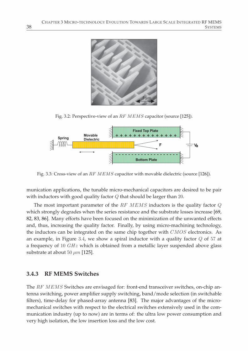
38CHAPTER 3 MICRO-TECHNOLOGY EVOLUTION TOWARDS LARGE SCALE INTEGRATED RF MEMS
SYSTEMS
Fig. 3.2: Perspective-view of an RF MEMS capacitor (source [125]).
Fig. 3.3: Cross-view of an RF MEMS capacitor with movable dielectric (source [126]).
munication applications, the tunable micro-mechanical capacitors are desired to be pair
with inductors with good quality factor Q that should be larger than 20.
The most important parameter of the RF MEMS inductors is the quality factor Q
which strongly degrades when the series resistance and the substrate losses increase [69,
82, 83, 86]. Many efforts have been focused on the minimization of the unwanted effects
and, thus, increasing the quality factor. Finally, by using micro-machining technology,
the inductors can be integrated on the same chip together with CMOS electronics. As
an example, in Figure 3.4, we show a spiral inductor with a quality factor Q of 57 at
a frequency of 10 GHz which is obtained from a metallic layer suspended above glass
substrate at about 50 µm [125].
3.4.3 RF MEMS Switches
The RF MEMS Switches are envisaged for: front-end transceiver switches, on-chip an-
tenna switching, power amplifier supply switching, band/mode selection (in switchable
filters), time-delay for phased-array antenna [83]. The major advantages of the micro-
mechanical switches with respect to the electrical switches extensively used in the com-
munication industry (up to now) are in terms of: the ultra low power consumption and
very high isolation, the low insertion loss and the low cost.
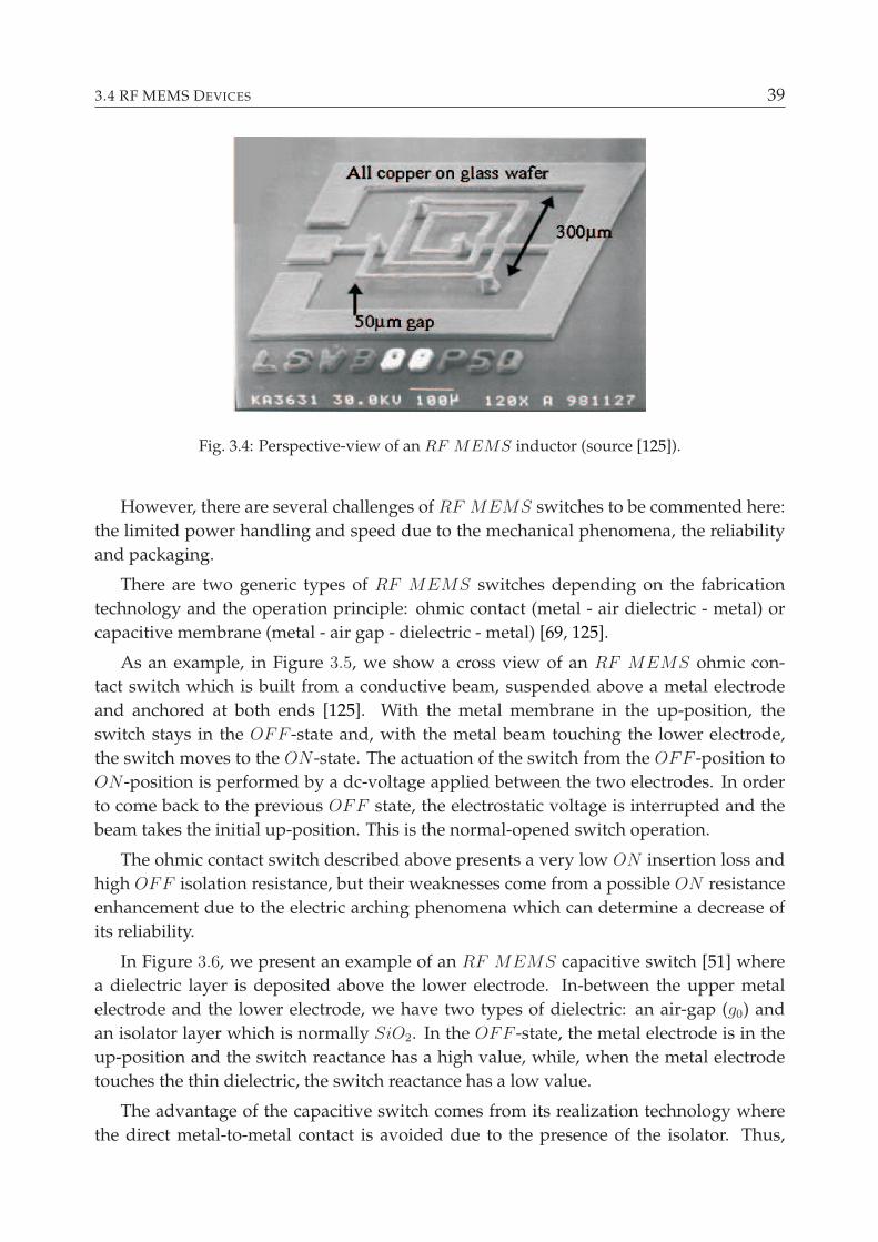
3.4 RF MEMS DEVICES 39
Fig. 3.4: Perspective-view of an RF MEMS inductor (source [125]).
However, there are several challenges of RF MEMS switches to be commented here:
the limited power handling and speed due to the mechanical phenomena, the reliability
and packaging.
There are two generic types of RF MEMS switches depending on the fabrication
technology and the operation principle: ohmic contact (metal - air dielectric - metal) or
capacitive membrane (metal - air gap - dielectric - metal) [69, 125].
As an example, in Figure 3.5, we show a cross view of an RF MEMS ohmic con-
tact switch which is built from a conductive beam, suspended above a metal electrode
and anchored at both ends [125]. With the metal membrane in the up-position, the
switch stays in the OFF -state and, with the metal beam touching the lower electrode,
the switch moves to the ON -state. The actuation of the switch from the OFF -position to
ON -position is performed by a dc-voltage applied between the two electrodes. In order
to come back to the previous OFF state, the electrostatic voltage is interrupted and the
beam takes the initial up-position. This is the normal-opened switch operation.
The ohmic contact switch described above presents a very low ON insertion loss and
high OFF isolation resistance, but their weaknesses come from a possible ON resistance
enhancement due to the electric arching phenomena which can determine a decrease of
its reliability.
In Figure 3.6, we present an example of an RF MEMS capacitive switch [51] where
a dielectric layer is deposited above the lower electrode. In-between the upper metal
electrode and the lower electrode, we have two types of dielectric: an air-gap (g0) and
an isolator layer which is normally SiO2. In the OFF -state, the metal electrode is in the
up-position and the switch reactance has a high value, while, when the metal electrode
touches the thin dielectric, the switch reactance has a low value.
The advantage of the capacitive switch comes from its realization technology where
the direct metal-to-metal contact is avoided due to the presence of the isolator. Thus,
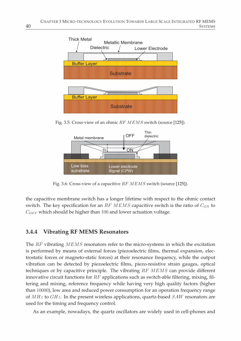
40CHAPTER 3 MICRO-TECHNOLOGY EVOLUTION TOWARDS LARGE SCALE INTEGRATED RF MEMS
SYSTEMS
Substrate
Substrate
Buffer Layer
Buffer Layer
Thick MetalMetallic Membrane
Lower ElectrodeDielectric
Fig. 3.5: Cross-view of an ohmic RF MEMS switch (source [125]).
Low losssubstrate
Lower electrodeSignal (CPW)
OFF
ON
Thindielectric
Metal membrane
g 0
Fig. 3.6: Cross-view of a capacitive RF MEMS switch (source [125]).
the capacitive membrane switch has a longer lifetime with respect to the ohmic contact
switch. The key specification for an RF MEMS capacitive switch is the ratio of CON to
COFF which should be higher than 100 and lower actuation voltage.
3.4.4 Vibrating RF MEMS Resonators
The RF vibrating MEMS resonators refer to the micro-systems in which the excitation
is performed by means of external forces (piezoelectric films, thermal expansion, elec-
trostatic forces or magneto-static forces) at their resonance frequency, while the output
vibration can be detected by piezoelectric films, piezo-resistive strain gauges, optical
techniques or by capacitive principle. The vibrating RF MEMS can provide different
innovative circuit functions for RF applications such as switch-able filtering, mixing, fil-
tering and mixing, reference frequency while having very high quality factors (higher
than 10000), low area and reduced power consumption for an operation frequency range
of MHz to GHz. In the present wireless applications, quartz-based SAW resonators are
used for the timing and frequency control.
As an example, nowadays, the quartz oscillators are widely used in cell-phones and
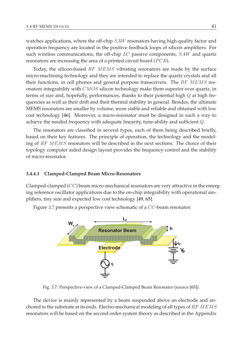
3.4 RF MEMS DEVICES 41
watches applications, where the off-chip SAW resonators having high quality factor and
operation frequency are located in the positive feedback loops of silicon amplifiers. For
such wireless communications, the off-chip LC passive components, SAW and quartz
resonators are increasing the area of a printed circuit board (PCB).
Today, the silicon-based RF MEMS vibrating resonators are made by the surface
micro-machining technology and they are intended to replace the quartz crystals and all
their functions, in cell phones and general purpose transceivers. The RF MEMS res-
onators integrability with CMOS silicon technology make them superior over quartz, in
terms of size and, hopefully, performances, thanks to their potential high Q at high fre-
quencies as well as their drift and their thermal stability in general. Besides, the ultimate
MEMS resonators are smaller by volume, more stable and reliable and obtained with low
cost technology [46]. Moreover, a micro-resonator must be designed in such a way to
achieve the needed frequency with adequate linearity, tune-ability and sufficient Q.
The resonators are classified in several types, each of them being described briefly,
based on their key features. The principle of operation, the technology and the model-
ing of RF MEMS resonators will be described in the next sections. The choice of their
topology computer aided design layout provides the frequency control and the stability
of micro-resonator.
3.4.4.1 Clamped-Clamped Beam Micro-Resonators
Clamped-clamped (CC) beam micro-mechanical resonators are very attractive in the emerg-
ing reference oscillator applications due to the on-chip integrability with operational am-
plifiers, tiny size and expected low cost technology [49, 65].
Figure 3.7 presents a perspective view schematic of a CC-beam resonator.
VP
VI
Resonator Beam
Electrode
L
hW
r
r
io
Fig. 3.7: Perspective-view of a Clamped-Clamped Beam Resonator (source [65]).
The device is mainly represented by a beam suspended above an electrode and an-
chored to the substrate at its ends. Electro-mechanical modeling of all types ofRF MEMS
resonators will be based on the second order system theory as described in the Appendix
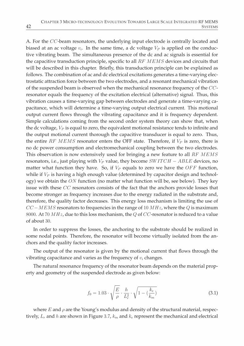
42CHAPTER 3 MICRO-TECHNOLOGY EVOLUTION TOWARDS LARGE SCALE INTEGRATED RF MEMS
SYSTEMS
A. For the CC-beam resonators, the underlying input electrode is centrally located and
biased at an ac voltage vi. In the same time, a dc voltage VP is applied on the conduc-
tive vibrating beam. The simultaneous presence of the dc and ac signals is essential for
the capacitive transduction principle, specific to all RF MEMS devices and circuits that
will be described in this chapter. Briefly, this transduction principle can be explained as
follows. The combination of ac and dc electrical excitations generates a time-varying elec-
trostatic attraction force between the two electrodes, and a resonant mechanical vibration
of the suspended beam is observed when the mechanical resonance frequency of the CC-
resonator equals the frequency of the excitation electrical (alternative) signal. Thus, this
vibration causes a time-varying gap between electrodes and generate a time-varying ca-
pacitance, which will determine a time-varying output electrical current. This motional
output current flows through the vibrating capacitance and it is frequency dependent.
Simple calculations coming from the second order system theory can show that, when
the dc voltage, VP is equal to zero, the equivalent motional resistance tends to infinite and
the output motional current thorough the capacitive transducer is equal to zero. Thus,
the entire RF MEMS resonator enters the OFF state. Therefore, if VP is zero, there is
no dc power consumption and electromechanical coupling between the two electrodes.
This observation is now extensively used for bringing a new feature to all RF MEMS
resonators, i.e., just playing with VP value, they become SWITCH − ABLE devices, no
matter what function they have. So, if VP equals to zero we have the OFF function,
while if VP is having a high enough value (determined by capacitor design and technol-
ogy) we obtain the ON function (no matter what function will be, see below). They key
issue with these CC resonators consists of the fact that the anchors provide losses that
become stronger as frequency increases due to the energy radiated in the substrate and,
therefore, the quality factor decreases. This energy loss mechanism is limiting the use of
CC−MEMS resonators to frequencies in the range of 10MHz, where theQ is maximum
8000. At 70MHz, due to this loss mechanism, theQ of CC-resonator is reduced to a value
of about 30.
In order to suppress the losses, the anchoring to the substrate should be realized in
some nodal points. Therefore, the resonator will become virtually isolated from the an-
chors and the quality factor increases.
The output of the resonator is given by the motional current that flows through the
vibrating capacitance and varies as the frequency of vi changes.
The natural resonance frequency of the resonator beam depends on the material prop-
erty and geometry of the suspended electrode as given below:
f0 = 1.03 ·√
E
ρ· hL2
r
·√
1 − (ke
km
) (3.1)
where E and ρ are the Young’s modulus and density of the structural material, respec-
tively, Lr and h are shown in Figure 3.7, km and ke represent the mechanical and electrical
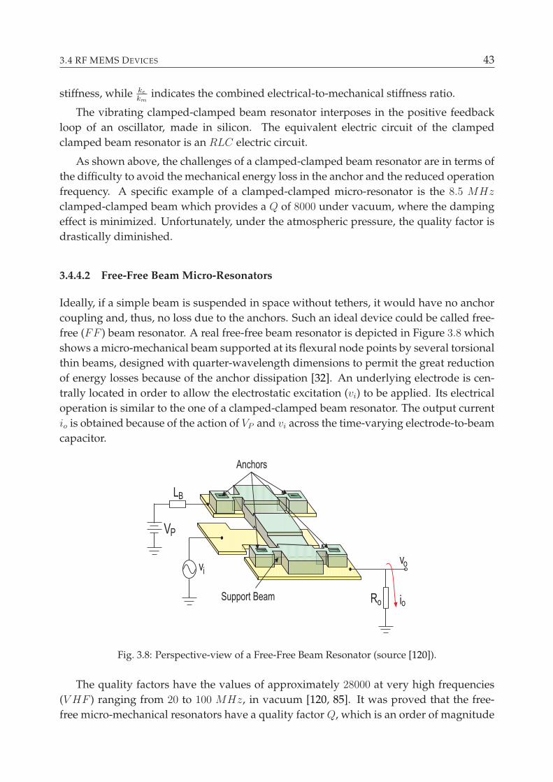
3.4 RF MEMS DEVICES 43
stiffness, while kekm
indicates the combined electrical-to-mechanical stiffness ratio.
The vibrating clamped-clamped beam resonator interposes in the positive feedback
loop of an oscillator, made in silicon. The equivalent electric circuit of the clamped
clamped beam resonator is an RLC electric circuit.
As shown above, the challenges of a clamped-clamped beam resonator are in terms of
the difficulty to avoid the mechanical energy loss in the anchor and the reduced operation
frequency. A specific example of a clamped-clamped micro-resonator is the 8.5 MHz
clamped-clamped beam which provides a Q of 8000 under vacuum, where the damping
effect is minimized. Unfortunately, under the atmospheric pressure, the quality factor is
drastically diminished.
3.4.4.2 Free-Free Beam Micro-Resonators
Ideally, if a simple beam is suspended in space without tethers, it would have no anchor
coupling and, thus, no loss due to the anchors. Such an ideal device could be called free-
free (FF ) beam resonator. A real free-free beam resonator is depicted in Figure 3.8 which
shows a micro-mechanical beam supported at its flexural node points by several torsional
thin beams, designed with quarter-wavelength dimensions to permit the great reduction
of energy losses because of the anchor dissipation [32]. An underlying electrode is cen-
trally located in order to allow the electrostatic excitation (vi) to be applied. Its electrical
operation is similar to the one of a clamped-clamped beam resonator. The output current
io is obtained because of the action of VP and vi across the time-varying electrode-to-beam
capacitor.
VP
v
Anchors
Support Beam
L
R i
v
B
i
o
o
o
Fig. 3.8: Perspective-view of a Free-Free Beam Resonator (source [120]).
The quality factors have the values of approximately 28000 at very high frequencies
(V HF ) ranging from 20 to 100 MHz, in vacuum [120, 85]. It was proved that the free-
free micro-mechanical resonators have a quality factor Q, which is an order of magnitude
44CHAPTER 3 MICRO-TECHNOLOGY EVOLUTION TOWARDS LARGE SCALE INTEGRATED RF MEMS
SYSTEMS
higher than the Q of clamped-clamped-beam versions due to the diminished anchor dis-
sipation.
A convenient design of a free-free beam resonator needs a good geometry which pro-
vides the desired frequency and assure a good support isolation in order to avoid any
stick between beam and underlying electrode when VP is applied. The procedure of res-
onator design is dependent on the range of frequency as it follows. At low frequencies,
when the beam is long and thin, the Euler-Bernoulli equation is used to calculate the
fundamental frequency, while the Timoshenko method is more appropriate to higher fre-
quencies because of its ability to model the shear displacements and rotary inertias. In the
same manner used in the previous CC resonator, the RLC equivalent circuit is realized.
The most critical element in a micro-mechanical resonator is the motional resistance that
should be low, because of the impedance matching consideration and thus, due to the
maximum power transmission in and from the micro-mechanical system. An alternative
to reduce it would be to use higher-mode free-free beam micro-mechanical resonators.
The latter provide higher dynamic range, power handling and an improved quality fac-
tor, which did not decrease with the increase in frequency to about 100 MHz. They have
two or three electrodes underneath the beams and centered between each adjacent node
pair, and three or four torsional-mode supports attached at the nodal locations. The ar-
rangement depends on the mode used by the designer. A higher mode involves a higher
number of electrodes and support beams.
According to the above description, Figure 3.9 shows a measured spectrum of a 92.25
MHz free-free beam micro-resonator for which the quality factor was found to be equal
to 7450.
Fig. 3.9: Measured Frequency Characteristic of a Free-Free Beam Resonator (source [120]).
Despite the improvements of a higher mode free-free resonator with respect to the
clamped clamped beam resonator, the performances are still weak, especially at higher
frequencies than 100 MHz. Therefore, other types of resonators are stringent required.
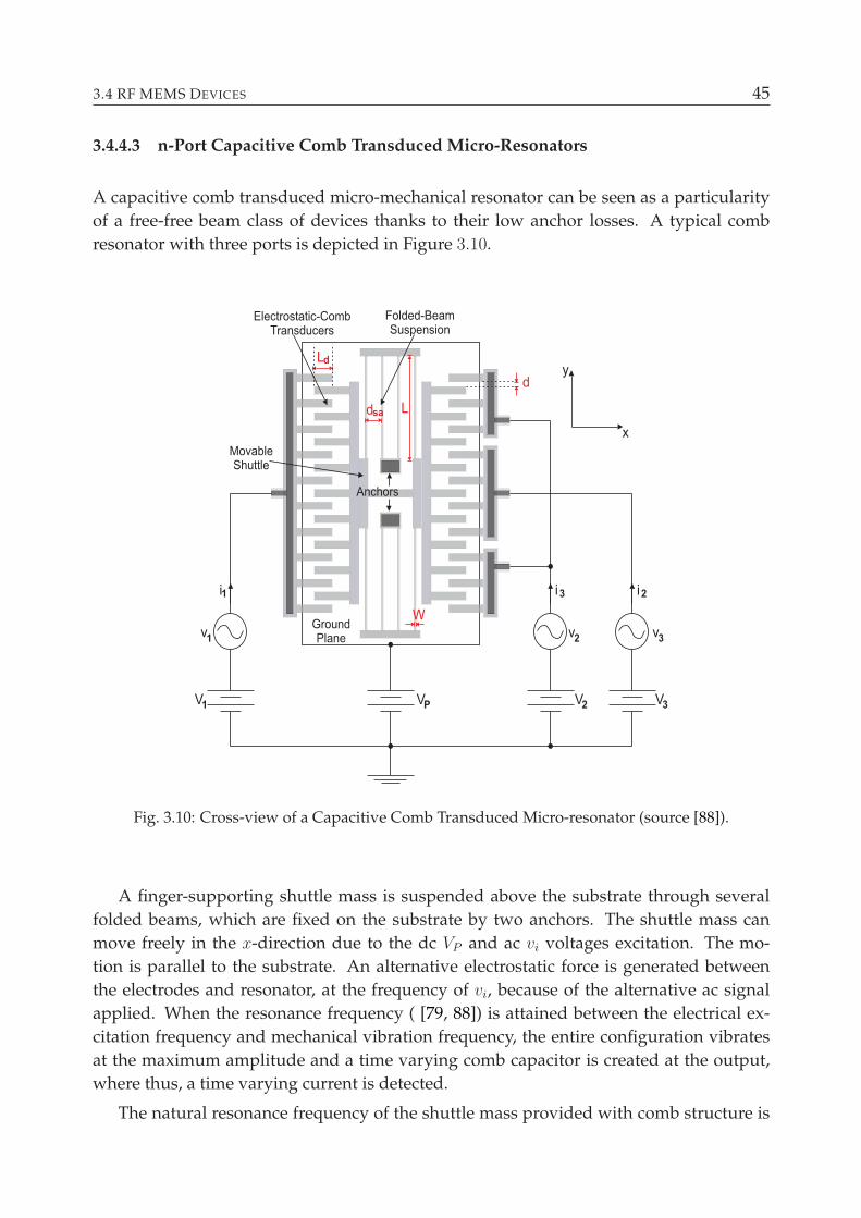
3.4 RF MEMS DEVICES 45
3.4.4.3 n-Port Capacitive Comb Transduced Micro-Resonators
A capacitive comb transduced micro-mechanical resonator can be seen as a particularity
of a free-free beam class of devices thanks to their low anchor losses. A typical comb
resonator with three ports is depicted in Figure 3.10.
Fig. 3.10: Cross-view of a Capacitive Comb Transduced Micro-resonator (source [88]).
A finger-supporting shuttle mass is suspended above the substrate through several
folded beams, which are fixed on the substrate by two anchors. The shuttle mass can
move freely in the x-direction due to the dc VP and ac vi voltages excitation. The mo-
tion is parallel to the substrate. An alternative electrostatic force is generated between
the electrodes and resonator, at the frequency of vi, because of the alternative ac signal
applied. When the resonance frequency ( [79, 88]) is attained between the electrical ex-
citation frequency and mechanical vibration frequency, the entire configuration vibrates
at the maximum amplitude and a time varying comb capacitor is created at the output,
where thus, a time varying current is detected.
The natural resonance frequency of the shuttle mass provided with comb structure is
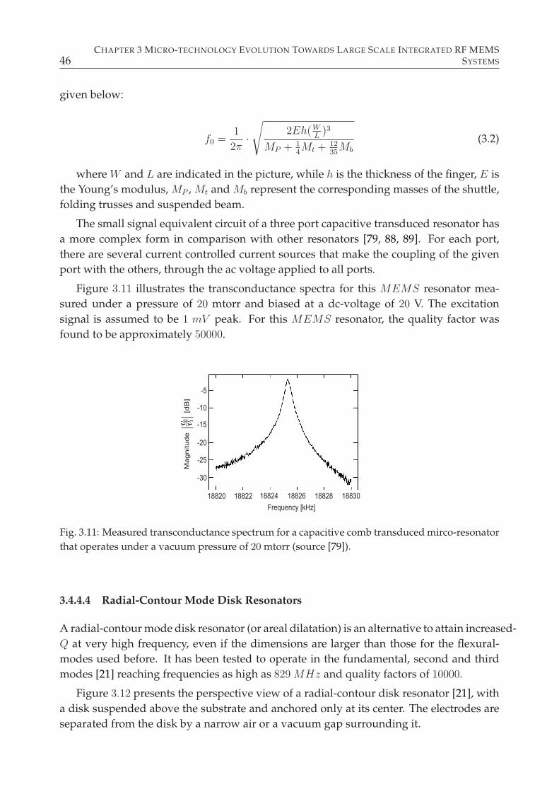
46CHAPTER 3 MICRO-TECHNOLOGY EVOLUTION TOWARDS LARGE SCALE INTEGRATED RF MEMS
SYSTEMS
given below:
f0 =1
2π·√
2Eh(WL
)3
MP + 14Mt + 12
35Mb
(3.2)
where W and L are indicated in the picture, while h is the thickness of the finger, E is
the Young’s modulus, MP , Mt and Mb represent the corresponding masses of the shuttle,
folding trusses and suspended beam.
The small signal equivalent circuit of a three port capacitive transduced resonator has
a more complex form in comparison with other resonators [79, 88, 89]. For each port,
there are several current controlled current sources that make the coupling of the given
port with the others, through the ac voltage applied to all ports.
Figure 3.11 illustrates the transconductance spectra for this MEMS resonator mea-
sured under a pressure of 20 mtorr and biased at a dc-voltage of 20 V. The excitation
signal is assumed to be 1 mV peak. For this MEMS resonator, the quality factor was
found to be approximately 50000.
Fig. 3.11: Measured transconductance spectrum for a capacitive comb transduced mirco-resonator
that operates under a vacuum pressure of 20 mtorr (source [79]).
3.4.4.4 Radial-Contour Mode Disk Resonators
A radial-contour mode disk resonator (or areal dilatation) is an alternative to attain increased-
Q at very high frequency, even if the dimensions are larger than those for the flexural-
modes used before. It has been tested to operate in the fundamental, second and third
modes [21] reaching frequencies as high as 829 MHz and quality factors of 10000.
Figure 3.12 presents the perspective view of a radial-contour disk resonator [21], with
a disk suspended above the substrate and anchored only at its center. The electrodes are
separated from the disk by a narrow air or a vacuum gap surrounding it.
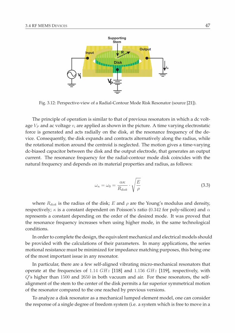
3.4 RF MEMS DEVICES 47
VP
VI
R
SupportingStem
OutputInput
Disk
io
Fig. 3.12: Perspective-view of a Radial-Contour Mode Risk Resonator (source [21]).
The principle of operation is similar to that of previous resonators in which a dc volt-
age VP and ac voltage vi are applied as shown in the picture. A time varying electrostatic
force is generated and acts radially on the disk, at the resonance frequency of the de-
vice. Consequently, the disk expands and contracts alternatively along the radius, while
the rotational motion around the centroid is neglected. The motion gives a time-varying
dc-biased capacitor between the disk and the output electrode, that generates an output
current. The resonance frequency for the radial-contour mode disk coincides with the
natural frequency and depends on its material properties and radius, as follows:
ωn = ω0 =ακ
Rdisk
·√
E
ρ(3.3)
where Rdisk is the radius of the disk; E and ρ are the Young’s modulus and density,
respectively; κ is a constant dependent on Poisson’s ratio (0.342 for poly-silicon) and α
represents a constant depending on the order of the desired mode. It was proved that
the resonance frequency increases when using higher mode, in the same technological
conditions.
In order to complete the design, the equivalent mechanical and electrical models should
be provided with the calculations of their parameters. In many applications, the series
motional resistance must be minimized for impedance matching purposes, this being one
of the most important issue in any resonator.
In particular, there are a few self-aligned vibrating micro-mechanical resonators that
operate at the frequencies of 1.14 GHz [118] and 1.156 GHz [119], respectively, with
Q’s higher than 1500 and 2650 in both vacuum and air. For these resonators, the self-
alignment of the stem to the center of the disk permits a far superior symmetrical motion
of the resonator compared to the one reached by previous versions.
To analyze a disk resonator as a mechanical lumped element model, one can consider
the response of a single degree of freedom system (i.e. a system which is free to move in a
48CHAPTER 3 MICRO-TECHNOLOGY EVOLUTION TOWARDS LARGE SCALE INTEGRATED RF MEMS
SYSTEMS
single direction as it is shown in Figure A.1) to the harmonic excitation, as written below:
m · d2y(t)
dt2+ c · dy(t)
dt+ k · y(t) = Fel(t) (3.4)
where y(t) is the displacement of the system as a function of time, Fel(t) is the force
exerted on the resonator, m denotes tge system mass, c is the damping coefficient and k
represents the mechanical spring constant.
The equation (3.7) can be rewritten as a function of the resonant natural frequency
ωn =√
km
, the quality factor Q = ωnmc
=√
kmc
and the damping ratio ξ = c
2√
kmre, as
follows:
d2y(t)
dt2+ 2ξωn · dy(t)
dt+ ω2
n · y(t) =ω2
n
k· Fel(t) (3.5)
Due to the dc voltage VP and ac voltage vi, a time varying electrostatic force is gener-
ated and acts radially on the disk at the resonance frequency of the device:
Fel =(VP − vi)
2
2· ∂C1
∂r(3.6)
where ∂C1
∂rdenotes the change in electrode-to-resonator overlap capacitance per unit
radial displacement at the input port.
By applying a periodic excitation voltage vi, of the form Vicos(ωit), and by maintaining
the constant dc voltage VP , the above equation will be:
Fel =∂C1
∂r[(V 2
P
2+V 2
i
4) − VPVicos(ωit) +
V 2i cos(2ωit)
4] (3.7)
One can observe three terms in the equation (3.10). The first term is a dc quantity
which has a small effect on high frequency oscillations. The second term shows the elec-
trical excitation at the frequency of oscillation ωi, being very important for filter and tank
circuit applications. The third term represents an harmonic force at a frequency away
from ωi and depends only on the ac signal. Consequently, the amplitude of the harmonic
is small enough to degrade the resonator performance and thus, can be neglected in the
model used in our work. As a conclusion, the relation of generated force (3.10) will be
simplified to:
Fel = −VP
∂C1
∂rvi (3.8)
Accordingly, the disk expands and contracts alternatively along the radius, while the
rotational motion around the centroid is neglected. The motion gives a time-varying dc-
biased capacitor between disk and output electrode that generates an output current as
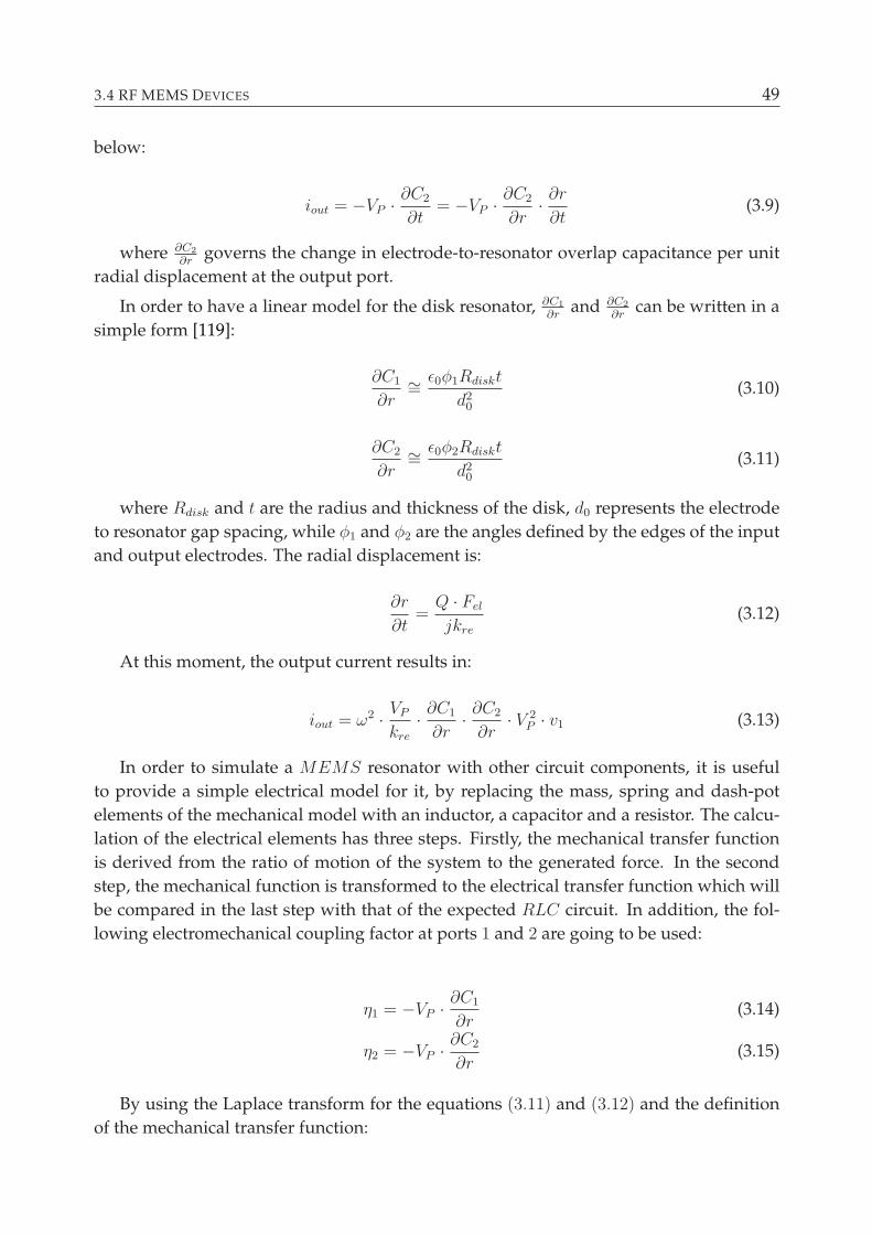
3.4 RF MEMS DEVICES 49
below:
iout = −VP · ∂C2
∂t= −VP · ∂C2
∂r· ∂r∂t
(3.9)
where ∂C2
∂rgoverns the change in electrode-to-resonator overlap capacitance per unit
radial displacement at the output port.
In order to have a linear model for the disk resonator, ∂C1
∂rand ∂C2
∂rcan be written in a
simple form [119]:
∂C1
∂r∼= ǫ0φ1Rdiskt
d20
(3.10)
∂C2
∂r∼= ǫ0φ2Rdiskt
d20
(3.11)
where Rdisk and t are the radius and thickness of the disk, d0 represents the electrode
to resonator gap spacing, while φ1 and φ2 are the angles defined by the edges of the input
and output electrodes. The radial displacement is:
∂r
∂t=Q · Fel
jkre
(3.12)
At this moment, the output current results in:
iout = ω2 · VP
kre
· ∂C1
∂r· ∂C2
∂r· V 2
P · v1 (3.13)
In order to simulate a MEMS resonator with other circuit components, it is useful
to provide a simple electrical model for it, by replacing the mass, spring and dash-pot
elements of the mechanical model with an inductor, a capacitor and a resistor. The calcu-
lation of the electrical elements has three steps. Firstly, the mechanical transfer function
is derived from the ratio of motion of the system to the generated force. In the second
step, the mechanical function is transformed to the electrical transfer function which will
be compared in the last step with that of the expected RLC circuit. In addition, the fol-
lowing electromechanical coupling factor at ports 1 and 2 are going to be used:
η1 = −VP · ∂C1
∂r(3.14)
η2 = −VP · ∂C2
∂r(3.15)
By using the Laplace transform for the equations (3.11) and (3.12) and the definition
of the mechanical transfer function:
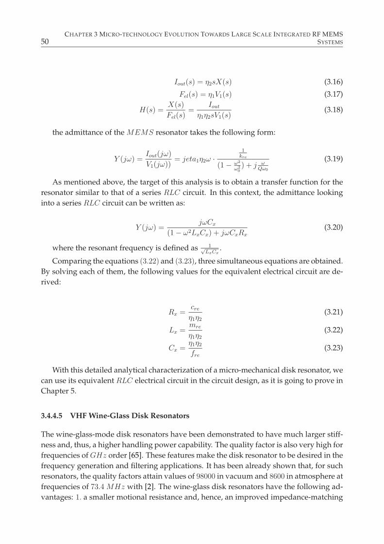
50CHAPTER 3 MICRO-TECHNOLOGY EVOLUTION TOWARDS LARGE SCALE INTEGRATED RF MEMS
SYSTEMS
Iout(s) = η2sX(s) (3.16)
Fel(s) = η1V1(s) (3.17)
H(s) =X(s)
Fel(s)=
Iout
η1η2sV1(s)(3.18)
the admittance of the MEMS resonator takes the following form:
Y (jω) =Iout(jω)
V1(jω))= jeta1η2ω ·
1kre
(1 − ω2
ω20) + j ω
Qω0
(3.19)
As mentioned above, the target of this analysis is to obtain a transfer function for the
resonator similar to that of a series RLC circuit. In this context, the admittance looking
into a series RLC circuit can be written as:
Y (jω) =jωCx
(1 − ω2LxCx) + jωCxRx
(3.20)
where the resonant frequency is defined as 1√LxCx
.
Comparing the equations (3.22) and (3.23), three simultaneous equations are obtained.
By solving each of them, the following values for the equivalent electrical circuit are de-
rived:
Rx =cre
η1η2
(3.21)
Lx =mre
η1η2
(3.22)
Cx =η1η2
fre
(3.23)
With this detailed analytical characterization of a micro-mechanical disk resonator, we
can use its equivalent RLC electrical circuit in the circuit design, as it is going to prove in
Chapter 5.
3.4.4.5 VHF Wine-Glass Disk Resonators
The wine-glass-mode disk resonators have been demonstrated to have much larger stiff-
ness and, thus, a higher handling power capability. The quality factor is also very high for
frequencies ofGHz order [65]. These features make the disk resonator to be desired in the
frequency generation and filtering applications. It has been already shown that, for such
resonators, the quality factors attain values of 98000 in vacuum and 8600 in atmosphere at
frequencies of 73.4 MHz with [2]. The wine-glass disk resonators have the following ad-
vantages: 1. a smaller motional resistance and, hence, an improved impedance-matching
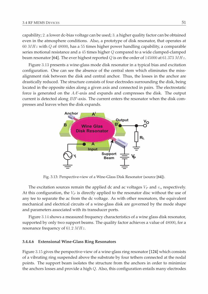
3.4 RF MEMS DEVICES 51
capability; 2. a lower dc-bias voltage can be used; 3. a higher quality factor can be obtained
even in the atmosphere conditions. Also, a prototype of disk resonator, that operates at
60 MHz with Q of 48000, has a 55 times higher power handling capability, a comparable
series motional resistance and a 45 times higher Q compared to a wide clamped-clamped
beam resonator [64]. The ever highest reportedQ is on the order of 145000 at 61.373MHz.
Figure 3.13 presents a wine-glass mode disk resonator in a typical bias and excitation
configuration. One can see the absence of the central stem which eliminates the miss-
alignment risk between the disk and central anchor. Thus, the losses in the anchor are
drastically reduced. The structure consists of four electrodes surrounding the disk, being
located in the opposite sides along a given axis and connected in pairs. The electrostatic
force is generated on the AA′-axis and expands and compresses the disk. The output
current is detected along BB′-axis. The current enters the resonator when the disk com-
presses and leaves when the disk expands.
RL
VO
VPVI
Input
Output
Anchor
Wine GlasDisk Resonator
SupportBeam
A
A
BB
I
I
Fig. 3.13: Perspective-view of a Wine-Glass Disk Resonator (source [64]).
The excitation sources remain the applied dc and ac voltages VP and vi, respectively.
At this configuration, the VP is directly applied to the resonator disc without the use of
any tee to separate the ac from the dc voltage. As with other resonators, the equivalent
mechanical and electrical circuits of a wine-glass disk are governed by the mode shape
and parameters associated with its transducer ports.
Figure 3.14 shows a measured frequency characteristics of a wine glass disk resonator,
supported by only two support beams. The quality factor achieves a value of 48000, for a
resonance frequency of 61.2 MHz.
3.4.4.6 Extensional Wine-Glass Ring Resonators
Figure 3.15 gives the perspective-view of a wine-glass ring resonator [124] which consists
of a vibrating ring suspended above the substrate by four tethers connected at the nodal
points. The support beam isolates the structure from the anchors in order to minimize
the anchors losses and provide a high Q. Also, this configuration entails many electrodes
52CHAPTER 3 MICRO-TECHNOLOGY EVOLUTION TOWARDS LARGE SCALE INTEGRATED RF MEMS
SYSTEMS
Fig. 3.14: Measured frequency characteristics of a wine glass disk resonator (source [64]).
surrounding the ring, in both inside and outside parts, with the purpose to increase the
area of overlapping capacitance. The difference between wine-glass disk and ring res-
onators consists of the fact that the electrode-to-resonator overlap area is only on outside
for the disk structure while the overlap area is formed on inside and outside part for the
ring counterpart.
VP
RL
VI
VI
RL
io
io Support Beam
RingResonator
InnerElectrode
OuterElectrode
Fig. 3.15: Perspective-view of a Wine-Glass Ring Resonator (source [124]).
To excite the resonator, a dc-voltage VP is applied to the ring, while the ac-voltage
vi drops on the two opposite electrodes. Further, a time varying electrostatic force ap-
pears at the frequency of vi, when the device is resonating. Due to dc-biased VP and
ac-voltage vi, at the resonance frequency, a time-varying capacitance obtained between
the electrodes and resonator will generate an output current that is sensed by the other
opposite electrodes. Shortly, the principle of operation is as follows: time-varying electri-
cal input signals (voltages) are generating time-varying electrostatic forces, determining
time-varying capacitances between electrodes and vibrating resonator which are giving
the time-varying output currents. Mechanically, the system is modeled by a spring-mass-
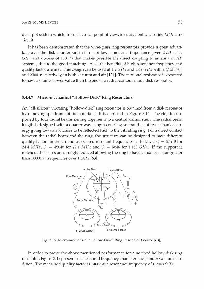
3.4 RF MEMS DEVICES 53
dash-pot system which, from electrical point of view, is equivalent to a series-LCR tank
circuit.
It has been demonstrated that the wine-glass ring resonators provide a great advan-
tage over the disk counterpart in terms of lower motional impedance (even 2 kΩ at 1.2
GHz and dc-bias of 100 V ) that makes possible the direct coupling to antenna in RF
systems, due to the good matching. Also, the benefits of high resonance frequency and
quality factor are met. This design can be used at 1.2 GHz and 1.47 GHz with a Q of 3700
and 2300, respectively, in both vacuum and air [124]. The motional resistance is expected
to have a 6 times lower value than the one of a radial-contour mode disk resonator.
3.4.4.7 Micro-mechanical ”Hollow-Disk” Ring Resonators
An ”all-silicon” vibrating ”hollow-disk” ring resonator is obtained from a disk resonator
by removing quadrants of its material as it is depicted in Figure 3.16. The ring is sup-
ported by four radial beams joining together into a central anchor stem. The radial beam
length is designed with a quarter wavelength coupling so that the entire mechanical en-
ergy going towards anchors to be reflected back to the vibrating ring. For a direct contact
between the radial beam and the ring, the structure can be designed to have different
quality factors in the air and associated resonant frequencies as follows: Q = 67519 for
24.4 MHz, Q = 48048 for 72.1 MHz and Q = 5846 for 1.169 GHz. If the support is
notched, the losses are strongly reduced allowing the ring to have a quality factor greater
than 10000 at frequencies over 1 GHz [63].
Fig. 3.16: Micro-mechanical ”Hollow-Disk” Ring Resonator (source [63]).
In order to prove the above-mentioned performance for a notched hollow-disk ring
resonator, Figure 3.17 presents its measured frequency characteristics, under vacuum con-
dition. The measured quality factor is 14603 at a resonance frequency of 1.2048 GHz.
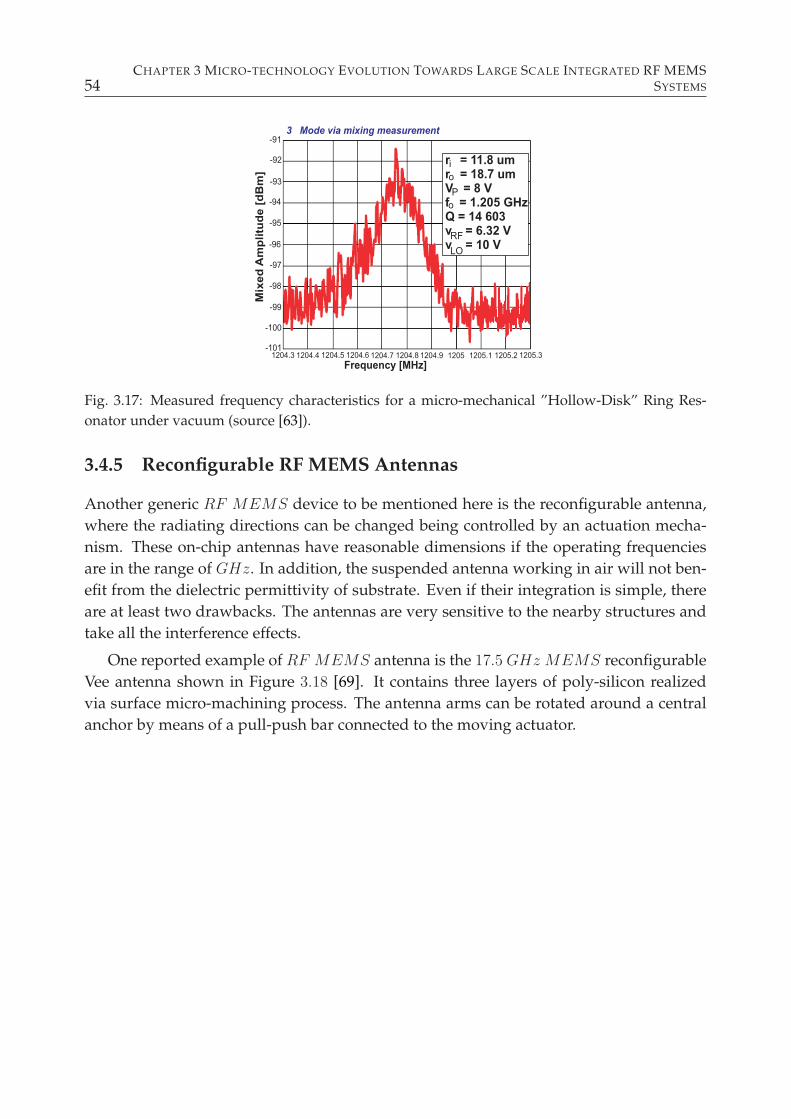
54CHAPTER 3 MICRO-TECHNOLOGY EVOLUTION TOWARDS LARGE SCALE INTEGRATED RF MEMS
SYSTEMS
r = 11.8 umr = 18.7 umV = 8 Vf = 1.205 GHzQ = 14 603v = 6.32 Vv = 10 V
i
o
o
P
RF
LO
3 Mode via mixing measurement
Frequency [MHz]
Mix
ed
Am
pli
tud
e [
dB
m]
-91
-92
-93
-94
-95
-96
-97
-98
-99
-100
-1011204.3 1204.4 1204.5 1204.6 1204.7 1204.8 1204.9 1205 1205.1 1205.2 1205.3
Fig. 3.17: Measured frequency characteristics for a micro-mechanical ”Hollow-Disk” Ring Res-
onator under vacuum (source [63]).
3.4.5 Reconfigurable RF MEMS Antennas
Another generic RF MEMS device to be mentioned here is the reconfigurable antenna,
where the radiating directions can be changed being controlled by an actuation mecha-
nism. These on-chip antennas have reasonable dimensions if the operating frequencies
are in the range of GHz. In addition, the suspended antenna working in air will not ben-
efit from the dielectric permittivity of substrate. Even if their integration is simple, there
are at least two drawbacks. The antennas are very sensitive to the nearby structures and
take all the interference effects.
One reported example of RF MEMS antenna is the 17.5 GHz MEMS reconfigurable
Vee antenna shown in Figure 3.18 [69]. It contains three layers of poly-silicon realized
via surface micro-machining process. The antenna arms can be rotated around a central
anchor by means of a pull-push bar connected to the moving actuator.
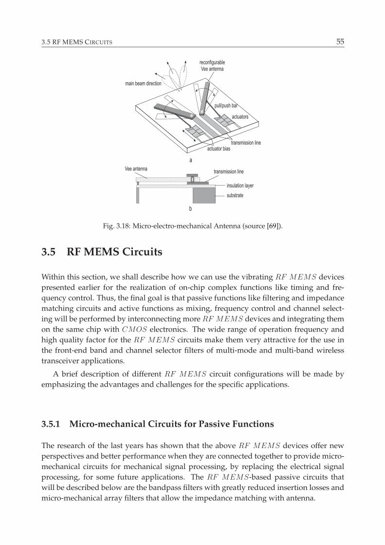
3.5 RF MEMS CIRCUITS 55
Fig. 3.18: Micro-electro-mechanical Antenna (source [69]).
3.5 RF MEMS Circuits
Within this section, we shall describe how we can use the vibrating RF MEMS devices
presented earlier for the realization of on-chip complex functions like timing and fre-
quency control. Thus, the final goal is that passive functions like filtering and impedance
matching circuits and active functions as mixing, frequency control and channel select-
ing will be performed by interconnecting more RF MEMS devices and integrating them
on the same chip with CMOS electronics. The wide range of operation frequency and
high quality factor for the RF MEMS circuits make them very attractive for the use in
the front-end band and channel selector filters of multi-mode and multi-band wireless
transceiver applications.
A brief description of different RF MEMS circuit configurations will be made by
emphasizing the advantages and challenges for the specific applications.
3.5.1 Micro-mechanical Circuits for Passive Functions
The research of the last years has shown that the above RF MEMS devices offer new
perspectives and better performance when they are connected together to provide micro-
mechanical circuits for mechanical signal processing, by replacing the electrical signal
processing, for some future applications. The RF MEMS-based passive circuits that
will be described below are the bandpass filters with greatly reduced insertion losses and
micro-mechanical array filters that allow the impedance matching with antenna.
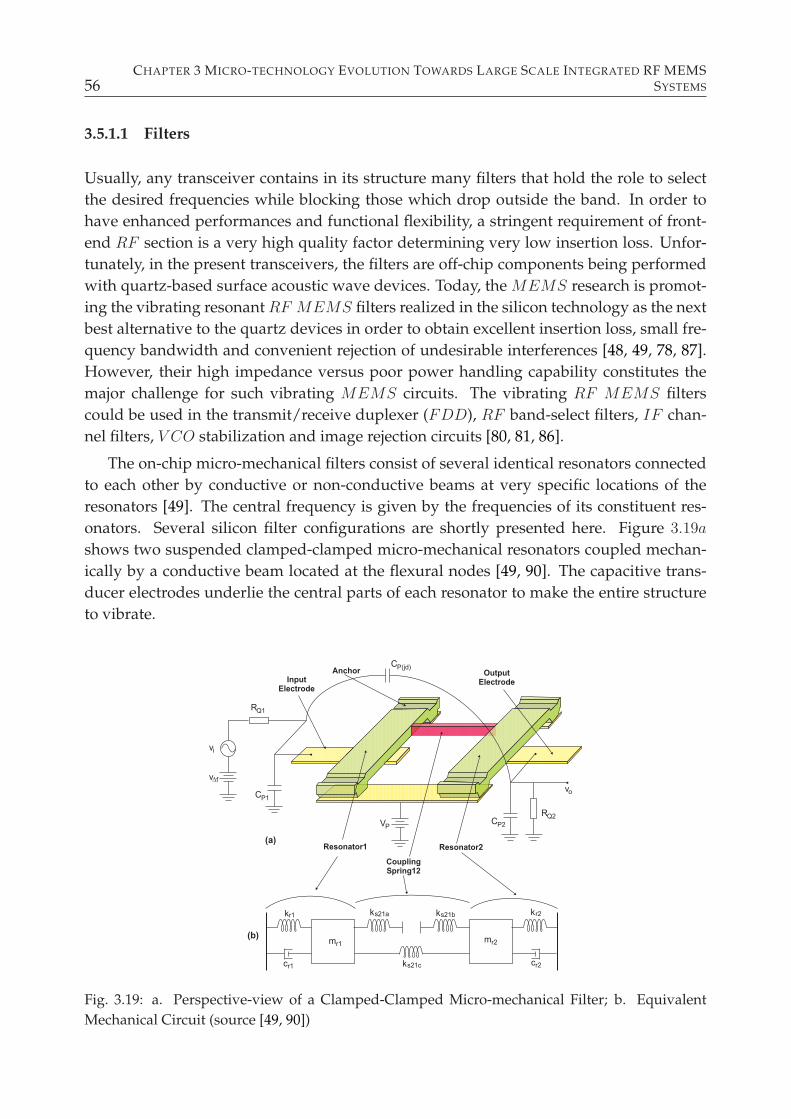
56CHAPTER 3 MICRO-TECHNOLOGY EVOLUTION TOWARDS LARGE SCALE INTEGRATED RF MEMS
SYSTEMS
3.5.1.1 Filters
Usually, any transceiver contains in its structure many filters that hold the role to select
the desired frequencies while blocking those which drop outside the band. In order to
have enhanced performances and functional flexibility, a stringent requirement of front-
end RF section is a very high quality factor determining very low insertion loss. Unfor-
tunately, in the present transceivers, the filters are off-chip components being performed
with quartz-based surface acoustic wave devices. Today, the MEMS research is promot-
ing the vibrating resonantRF MEMS filters realized in the silicon technology as the next
best alternative to the quartz devices in order to obtain excellent insertion loss, small fre-
quency bandwidth and convenient rejection of undesirable interferences [48, 49, 78, 87].
However, their high impedance versus poor power handling capability constitutes the
major challenge for such vibrating MEMS circuits. The vibrating RF MEMS filters
could be used in the transmit/receive duplexer (FDD), RF band-select filters, IF chan-
nel filters, V CO stabilization and image rejection circuits [80, 81, 86].
The on-chip micro-mechanical filters consist of several identical resonators connected
to each other by conductive or non-conductive beams at very specific locations of the
resonators [49]. The central frequency is given by the frequencies of its constituent res-
onators. Several silicon filter configurations are shortly presented here. Figure 3.19a
shows two suspended clamped-clamped micro-mechanical resonators coupled mechan-
ically by a conductive beam located at the flexural nodes [49, 90]. The capacitive trans-
ducer electrodes underlie the central parts of each resonator to make the entire structure
to vibrate.
Fig. 3.19: a. Perspective-view of a Clamped-Clamped Micro-mechanical Filter; b. Equivalent
Mechanical Circuit (source [49, 90])
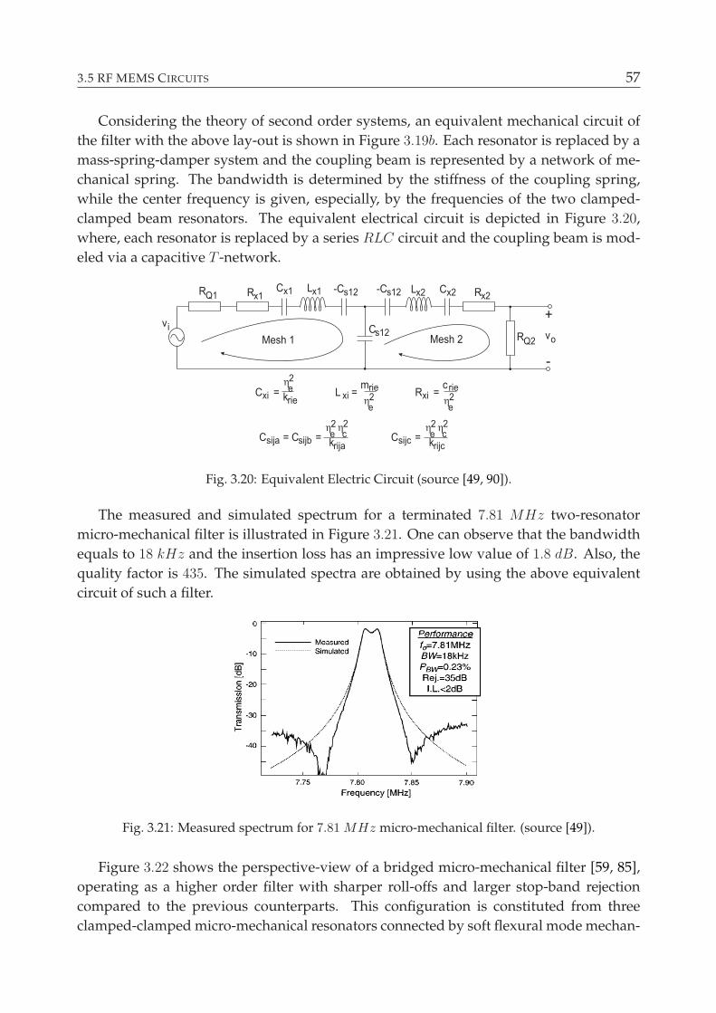
3.5 RF MEMS CIRCUITS 57
Considering the theory of second order systems, an equivalent mechanical circuit of
the filter with the above lay-out is shown in Figure 3.19b. Each resonator is replaced by a
mass-spring-damper system and the coupling beam is represented by a network of me-
chanical spring. The bandwidth is determined by the stiffness of the coupling spring,
while the center frequency is given, especially, by the frequencies of the two clamped-
clamped beam resonators. The equivalent electrical circuit is depicted in Figure 3.20,
where, each resonator is replaced by a series RLC circuit and the coupling beam is mod-
eled via a capacitive T -network.
Fig. 3.20: Equivalent Electric Circuit (source [49, 90]).
The measured and simulated spectrum for a terminated 7.81 MHz two-resonator
micro-mechanical filter is illustrated in Figure 3.21. One can observe that the bandwidth
equals to 18 kHz and the insertion loss has an impressive low value of 1.8 dB. Also, the
quality factor is 435. The simulated spectra are obtained by using the above equivalent
circuit of such a filter.
Fig. 3.21: Measured spectrum for 7.81 MHz micro-mechanical filter. (source [49]).
Figure 3.22 shows the perspective-view of a bridged micro-mechanical filter [59, 85],
operating as a higher order filter with sharper roll-offs and larger stop-band rejection
compared to the previous counterparts. This configuration is constituted from three
clamped-clamped micro-mechanical resonators connected by soft flexural mode mechan-
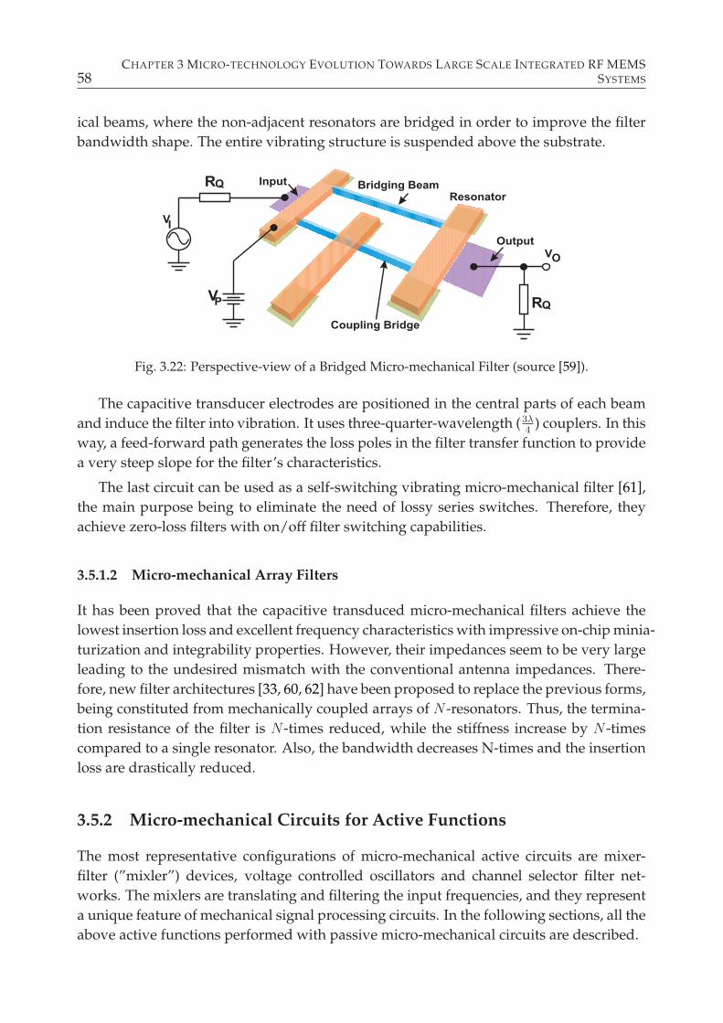
58CHAPTER 3 MICRO-TECHNOLOGY EVOLUTION TOWARDS LARGE SCALE INTEGRATED RF MEMS
SYSTEMS
ical beams, where the non-adjacent resonators are bridged in order to improve the filter
bandwidth shape. The entire vibrating structure is suspended above the substrate.
RQ
VO
RQ
VI
VP
Input
Output
Bridging BeamResonator
Coupling Bridge
Fig. 3.22: Perspective-view of a Bridged Micro-mechanical Filter (source [59]).
The capacitive transducer electrodes are positioned in the central parts of each beam
and induce the filter into vibration. It uses three-quarter-wavelength (3λ4
) couplers. In this
way, a feed-forward path generates the loss poles in the filter transfer function to provide
a very steep slope for the filter’s characteristics.
The last circuit can be used as a self-switching vibrating micro-mechanical filter [61],
the main purpose being to eliminate the need of lossy series switches. Therefore, they
achieve zero-loss filters with on/off filter switching capabilities.
3.5.1.2 Micro-mechanical Array Filters
It has been proved that the capacitive transduced micro-mechanical filters achieve the
lowest insertion loss and excellent frequency characteristics with impressive on-chip minia-
turization and integrability properties. However, their impedances seem to be very large
leading to the undesired mismatch with the conventional antenna impedances. There-
fore, new filter architectures [33, 60, 62] have been proposed to replace the previous forms,
being constituted from mechanically coupled arrays of N -resonators. Thus, the termina-
tion resistance of the filter is N -times reduced, while the stiffness increase by N -times
compared to a single resonator. Also, the bandwidth decreases N-times and the insertion
loss are drastically reduced.
3.5.2 Micro-mechanical Circuits for Active Functions
The most representative configurations of micro-mechanical active circuits are mixer-
filter (”mixler”) devices, voltage controlled oscillators and channel selector filter net-
works. The mixlers are translating and filtering the input frequencies, and they represent
a unique feature of mechanical signal processing circuits. In the following sections, all the
above active functions performed with passive micro-mechanical circuits are described.
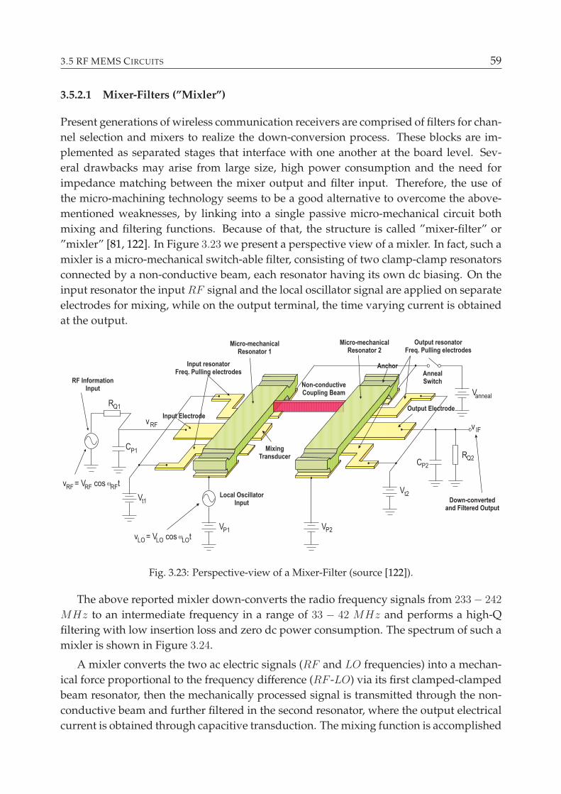
3.5 RF MEMS CIRCUITS 59
3.5.2.1 Mixer-Filters (”Mixler”)
Present generations of wireless communication receivers are comprised of filters for chan-
nel selection and mixers to realize the down-conversion process. These blocks are im-
plemented as separated stages that interface with one another at the board level. Sev-
eral drawbacks may arise from large size, high power consumption and the need for
impedance matching between the mixer output and filter input. Therefore, the use of
the micro-machining technology seems to be a good alternative to overcome the above-
mentioned weaknesses, by linking into a single passive micro-mechanical circuit both
mixing and filtering functions. Because of that, the structure is called ”mixer-filter” or
”mixler” [81, 122]. In Figure 3.23 we present a perspective view of a mixler. In fact, such a
mixler is a micro-mechanical switch-able filter, consisting of two clamp-clamp resonators
connected by a non-conductive beam, each resonator having its own dc biasing. On the
input resonator the input RF signal and the local oscillator signal are applied on separate
electrodes for mixing, while on the output terminal, the time varying current is obtained
at the output.
VP2
Vt1
Vanneal
Vt2
VP1
CP2
CP1
RQ1
RQ2
RF InformationInput
Input Electrode
Input resonatorFreq. Pulling electrodes
Micro-mechanicalResonator 1
Micro-mechanicalResonator 2
Non-conductiveCoupling Beam
AnchorAnnealSwitch
Output resonatorFreq. Pulling electrodes
MixingTransducer
Output Electrode
Down-convertedand Filtered Output
Local OscillatorInput
v IF
vRF
RFv = V cos tRFw
RF
LOv = V cos tLOw
LO
Fig. 3.23: Perspective-view of a Mixer-Filter (source [122]).
The above reported mixler down-converts the radio frequency signals from 233 − 242
MHz to an intermediate frequency in a range of 33 − 42 MHz and performs a high-Q
filtering with low insertion loss and zero dc power consumption. The spectrum of such a
mixler is shown in Figure 3.24.
A mixler converts the two ac electric signals (RF and LO frequencies) into a mechan-
ical force proportional to the frequency difference (RF -LO) via its first clamped-clamped
beam resonator, then the mechanically processed signal is transmitted through the non-
conductive beam and further filtered in the second resonator, where the output electrical
current is obtained through capacitive transduction. The mixing function is accomplished
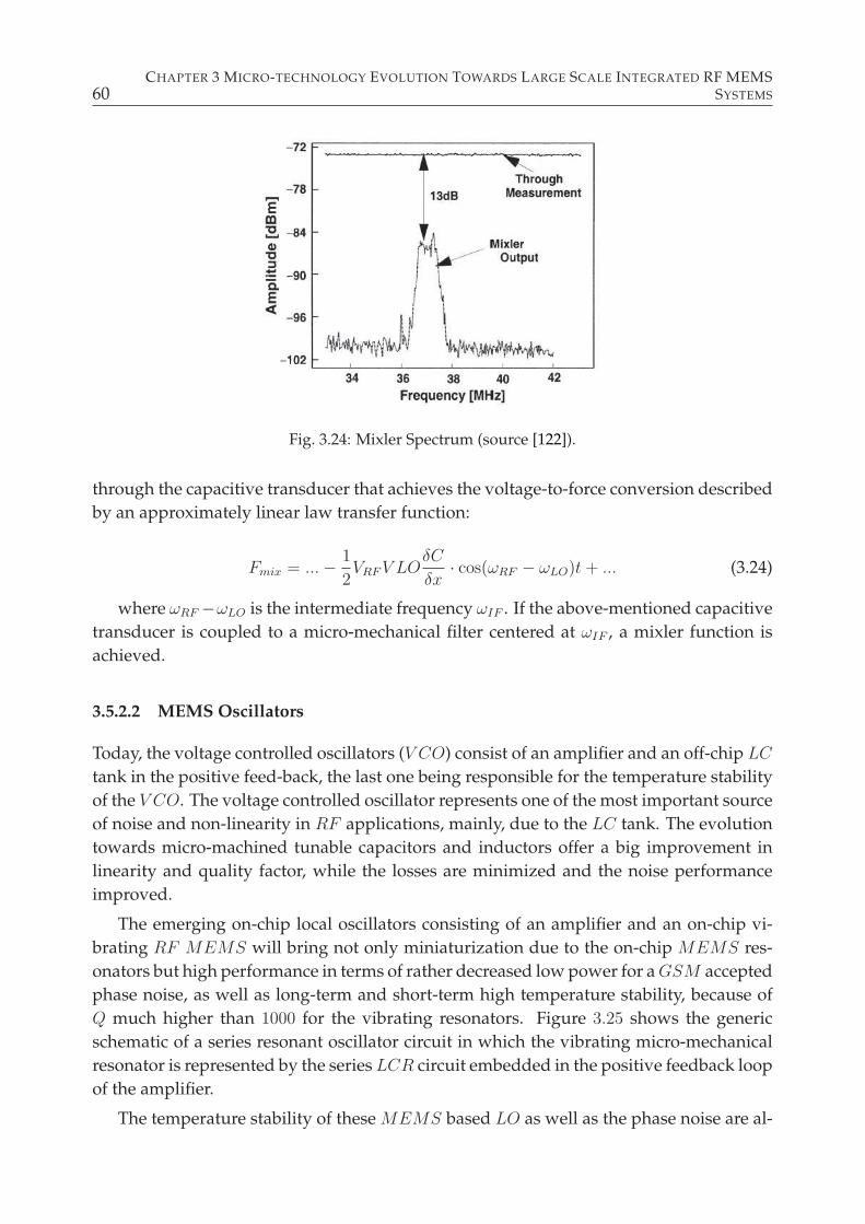
60CHAPTER 3 MICRO-TECHNOLOGY EVOLUTION TOWARDS LARGE SCALE INTEGRATED RF MEMS
SYSTEMS
Fig. 3.24: Mixler Spectrum (source [122]).
through the capacitive transducer that achieves the voltage-to-force conversion described
by an approximately linear law transfer function:
Fmix = ...− 1
2VRFV LO
δC
δx· cos(ωRF − ωLO)t+ ... (3.24)
where ωRF −ωLO is the intermediate frequency ωIF . If the above-mentioned capacitive
transducer is coupled to a micro-mechanical filter centered at ωIF , a mixler function is
achieved.
3.5.2.2 MEMS Oscillators
Today, the voltage controlled oscillators (V CO) consist of an amplifier and an off-chip LC
tank in the positive feed-back, the last one being responsible for the temperature stability
of the V CO. The voltage controlled oscillator represents one of the most important source
of noise and non-linearity in RF applications, mainly, due to the LC tank. The evolution
towards micro-machined tunable capacitors and inductors offer a big improvement in
linearity and quality factor, while the losses are minimized and the noise performance
improved.
The emerging on-chip local oscillators consisting of an amplifier and an on-chip vi-
brating RF MEMS will bring not only miniaturization due to the on-chip MEMS res-
onators but high performance in terms of rather decreased low power for aGSM accepted
phase noise, as well as long-term and short-term high temperature stability, because of
Q much higher than 1000 for the vibrating resonators. Figure 3.25 shows the generic
schematic of a series resonant oscillator circuit in which the vibrating micro-mechanical
resonator is represented by the series LCR circuit embedded in the positive feedback loop
of the amplifier.
The temperature stability of these MEMS based LO as well as the phase noise are al-
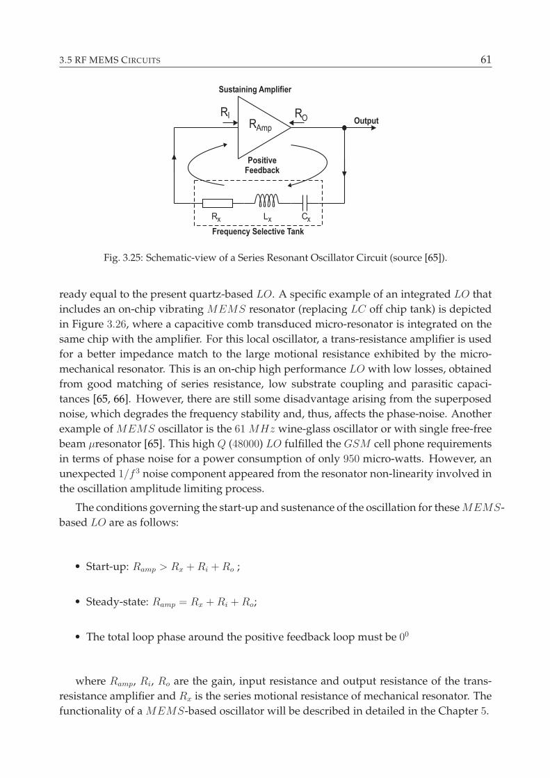
3.5 RF MEMS CIRCUITS 61
Fig. 3.25: Schematic-view of a Series Resonant Oscillator Circuit (source [65]).
ready equal to the present quartz-based LO. A specific example of an integrated LO that
includes an on-chip vibrating MEMS resonator (replacing LC off chip tank) is depicted
in Figure 3.26, where a capacitive comb transduced micro-resonator is integrated on the
same chip with the amplifier. For this local oscillator, a trans-resistance amplifier is used
for a better impedance match to the large motional resistance exhibited by the micro-
mechanical resonator. This is an on-chip high performance LO with low losses, obtained
from good matching of series resistance, low substrate coupling and parasitic capaci-
tances [65, 66]. However, there are still some disadvantage arising from the superposed
noise, which degrades the frequency stability and, thus, affects the phase-noise. Another
example of MEMS oscillator is the 61 MHz wine-glass oscillator or with single free-free
beam µresonator [65]. This high Q (48000) LO fulfilled the GSM cell phone requirements
in terms of phase noise for a power consumption of only 950 micro-watts. However, an
unexpected 1/f3 noise component appeared from the resonator non-linearity involved in
the oscillation amplitude limiting process.
The conditions governing the start-up and sustenance of the oscillation for theseMEMS-
based LO are as follows:
• Start-up: Ramp > Rx +Ri +Ro ;
• Steady-state: Ramp = Rx +Ri +Ro;
• The total loop phase around the positive feedback loop must be 00
where Ramp, Ri, Ro are the gain, input resistance and output resistance of the trans-
resistance amplifier and Rx is the series motional resistance of mechanical resonator. The
functionality of a MEMS-based oscillator will be described in detailed in the Chapter 5.
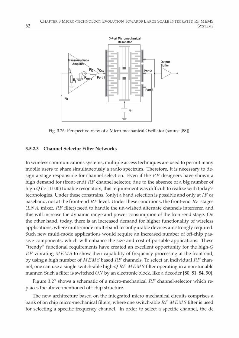
62CHAPTER 3 MICRO-TECHNOLOGY EVOLUTION TOWARDS LARGE SCALE INTEGRATED RF MEMS
SYSTEMS
Fig. 3.26: Perspective-view of a Micro-mechanical Oscillator (source [88]).
3.5.2.3 Channel Selector Filter Networks
In wireless communications systems, multiple access techniques are used to permit many
mobile users to share simultaneously a radio spectrum. Therefore, it is necessary to de-
sign a stage responsible for channel selection. Even if the RF designers have shown a
high demand for (front-end) RF channel selector, due to the absence of a big number of
highQ (> 10000) tunable resonators, this requirement was difficult to realize with today’s
technologies. Under these constrains, (only) a band selection is possible and only at IF or
baseband, not at the front-end RF level. Under these conditions, the front-end RF stages
(LNA, mixer, RF filter) need to handle the un-wished alternate channels interferer, and
this will increase the dynamic range and power consumption of the front-end stage. On
the other hand, today, there is an increased demand for higher functionality of wireless
applications, where multi-mode multi-band reconfigurable devices are strongly required.
Such new multi-mode applications would require an increased number of off-chip pas-
sive components, which will enhance the size and cost of portable applications. These
”trendy” functional requirements have created an excellent opportunity for the high-Q
RF vibrating MEMS to show their capability of frequency processing at the front end,
by using a high number of MEMS based RF channels. To select an individual RF chan-
nel, one can use a single switch-able high-Q RF MEMS filter operating in a non-tunable
manner. Such a filter is switched ON by an electronic block, like a decoder [80, 81, 84, 90].
Figure 3.27 shows a schematic of a micro-mechanical RF channel-selector which re-
places the above-mentioned off-chip structure.
The new architecture based on the integrated micro-mechanical circuits comprises a
bank of on chip micro-mechanical filters, where one switch-able RF MEMS filter is used
for selecting a specific frequency channel. In order to select a specific channel, the dc
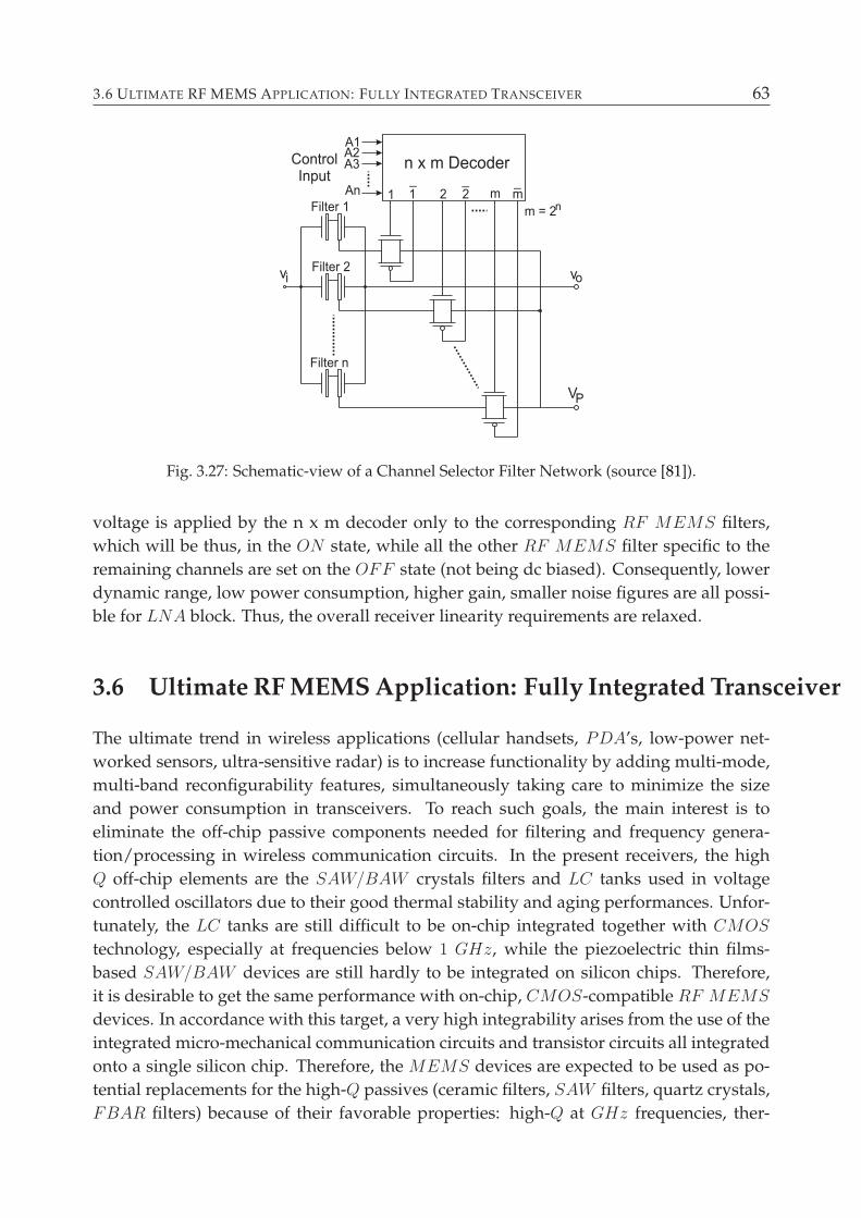
3.6 ULTIMATE RF MEMS APPLICATION: FULLY INTEGRATED TRANSCEIVER 63
Fig. 3.27: Schematic-view of a Channel Selector Filter Network (source [81]).
voltage is applied by the n x m decoder only to the corresponding RF MEMS filters,
which will be thus, in the ON state, while all the other RF MEMS filter specific to the
remaining channels are set on the OFF state (not being dc biased). Consequently, lower
dynamic range, low power consumption, higher gain, smaller noise figures are all possi-
ble for LNA block. Thus, the overall receiver linearity requirements are relaxed.
3.6 Ultimate RF MEMS Application: Fully Integrated Transceiver
The ultimate trend in wireless applications (cellular handsets, PDA’s, low-power net-
worked sensors, ultra-sensitive radar) is to increase functionality by adding multi-mode,
multi-band reconfigurability features, simultaneously taking care to minimize the size
and power consumption in transceivers. To reach such goals, the main interest is to
eliminate the off-chip passive components needed for filtering and frequency genera-
tion/processing in wireless communication circuits. In the present receivers, the high
Q off-chip elements are the SAW/BAW crystals filters and LC tanks used in voltage
controlled oscillators due to their good thermal stability and aging performances. Unfor-
tunately, the LC tanks are still difficult to be on-chip integrated together with CMOS
technology, especially at frequencies below 1 GHz, while the piezoelectric thin films-
based SAW/BAW devices are still hardly to be integrated on silicon chips. Therefore,
it is desirable to get the same performance with on-chip, CMOS-compatible RF MEMS
devices. In accordance with this target, a very high integrability arises from the use of the
integrated micro-mechanical communication circuits and transistor circuits all integrated
onto a single silicon chip. Therefore, the MEMS devices are expected to be used as po-
tential replacements for the high-Q passives (ceramic filters, SAW filters, quartz crystals,
FBAR filters) because of their favorable properties: high-Q at GHz frequencies, ther-
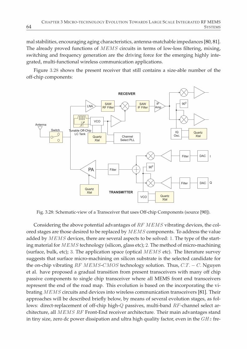
64CHAPTER 3 MICRO-TECHNOLOGY EVOLUTION TOWARDS LARGE SCALE INTEGRATED RF MEMS
SYSTEMS
mal stabilities, encouraging aging characteristics, antenna-matchable impedances [80, 81].
The already proved functions of MEMS circuits in terms of low-loss filtering, mixing,
switching and frequency generation are the driving force for the emerging highly inte-
grated, multi-functional wireless communication applications.
Figure 3.28 shows the present receiver that still contains a size-able number of the
off-chip components:
Fig. 3.28: Schematic-view of a Transceiver that uses Off-chip Components (source [90]).
Considering the above potential advantages of RF MEMS vibrating devices, the col-
ored stages are those desired to be replaced byMEMS components. To address the value
added by MEMS devices, there are several aspects to be solved: 1. The type of the start-
ing material forMEMS technology (silicon, glass etc); 2. The method of micro-machining
(surface, bulk, etc); 3. The application space (optical MEMS etc). The literature survey
suggests that surface micro-machining on silicon substrate is the selected candidate for
the on-chip vibrating RF MEMS-CMOS technology solution. Thus, C.T. − C. Nguyen
et al. have proposed a gradual transition from present transceivers with many off chip
passive components to single chip transceiver where all MEMS front end transceivers
represent the end of the road map. This evolution is based on the incorporating the vi-
brating MEMS circuits and devices into wireless communication transceivers [81]. Their
approaches will be described briefly below, by means of several evolution stages, as fol-
lows: direct-replacement of off-chip high-Q passives, multi-band RF -channel select ar-
chitecture, all MEMS RF Front-End receiver architecture. Their main advantages stand
in tiny size, zero dc power dissipation and ultra high quality factor, even in the GHz fre-
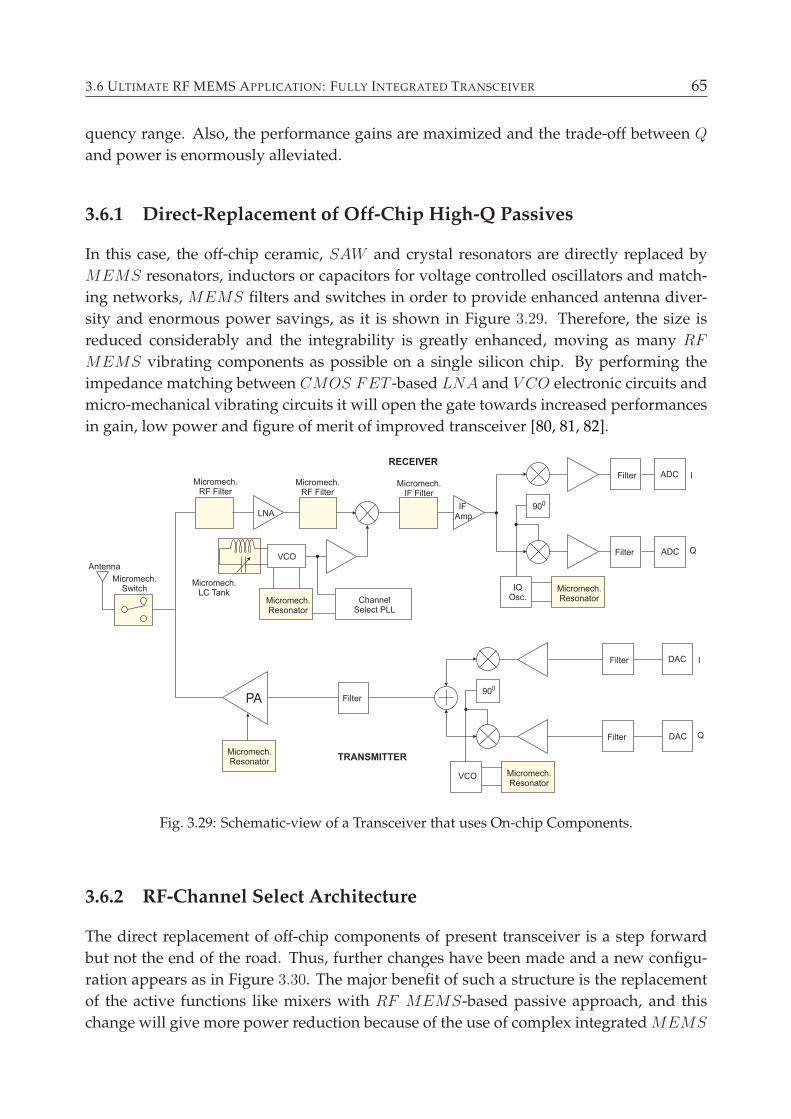
3.6 ULTIMATE RF MEMS APPLICATION: FULLY INTEGRATED TRANSCEIVER 65
quency range. Also, the performance gains are maximized and the trade-off between Q
and power is enormously alleviated.
3.6.1 Direct-Replacement of Off-Chip High-Q Passives
In this case, the off-chip ceramic, SAW and crystal resonators are directly replaced by
MEMS resonators, inductors or capacitors for voltage controlled oscillators and match-
ing networks, MEMS filters and switches in order to provide enhanced antenna diver-
sity and enormous power savings, as it is shown in Figure 3.29. Therefore, the size is
reduced considerably and the integrability is greatly enhanced, moving as many RF
MEMS vibrating components as possible on a single silicon chip. By performing the
impedance matching between CMOS FET -based LNA and V CO electronic circuits and
micro-mechanical vibrating circuits it will open the gate towards increased performances
in gain, low power and figure of merit of improved transceiver [80, 81, 82].
Fig. 3.29: Schematic-view of a Transceiver that uses On-chip Components.
3.6.2 RF-Channel Select Architecture
The direct replacement of off-chip components of present transceiver is a step forward
but not the end of the road. Thus, further changes have been made and a new configu-
ration appears as in Figure 3.30. The major benefit of such a structure is the replacement
of the active functions like mixers with RF MEMS-based passive approach, and this
change will give more power reduction because of the use of complex integrated MEMS
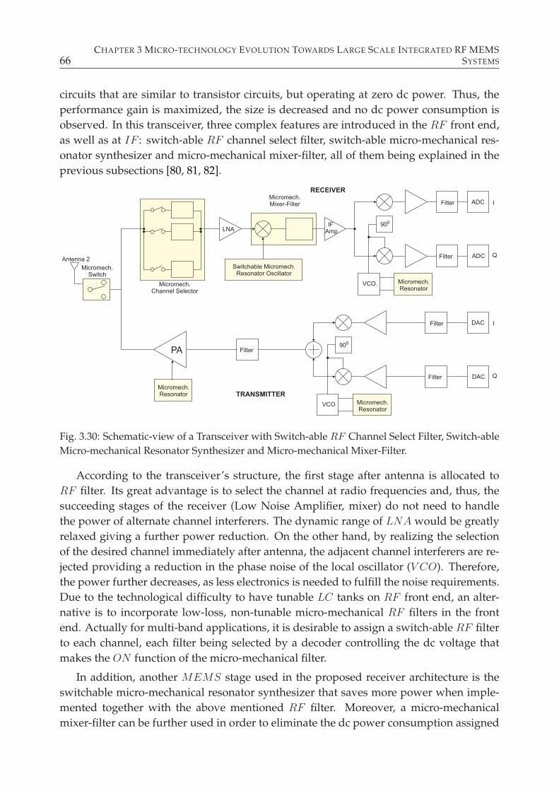
66CHAPTER 3 MICRO-TECHNOLOGY EVOLUTION TOWARDS LARGE SCALE INTEGRATED RF MEMS
SYSTEMS
circuits that are similar to transistor circuits, but operating at zero dc power. Thus, the
performance gain is maximized, the size is decreased and no dc power consumption is
observed. In this transceiver, three complex features are introduced in the RF front end,
as well as at IF : switch-able RF channel select filter, switch-able micro-mechanical res-
onator synthesizer and micro-mechanical mixer-filter, all of them being explained in the
previous subsections [80, 81, 82].
Fig. 3.30: Schematic-view of a Transceiver with Switch-able RF Channel Select Filter, Switch-able
Micro-mechanical Resonator Synthesizer and Micro-mechanical Mixer-Filter.
According to the transceiver’s structure, the first stage after antenna is allocated to
RF filter. Its great advantage is to select the channel at radio frequencies and, thus, the
succeeding stages of the receiver (Low Noise Amplifier, mixer) do not need to handle
the power of alternate channel interferers. The dynamic range of LNA would be greatly
relaxed giving a further power reduction. On the other hand, by realizing the selection
of the desired channel immediately after antenna, the adjacent channel interferers are re-
jected providing a reduction in the phase noise of the local oscillator (V CO). Therefore,
the power further decreases, as less electronics is needed to fulfill the noise requirements.
Due to the technological difficulty to have tunable LC tanks on RF front end, an alter-
native is to incorporate low-loss, non-tunable micro-mechanical RF filters in the front
end. Actually for multi-band applications, it is desirable to assign a switch-able RF filter
to each channel, each filter being selected by a decoder controlling the dc voltage that
makes the ON function of the micro-mechanical filter.
In addition, another MEMS stage used in the proposed receiver architecture is the
switchable micro-mechanical resonator synthesizer that saves more power when imple-
mented together with the above mentioned RF filter. Moreover, a micro-mechanical
mixer-filter can be further used in order to eliminate the dc power consumption assigned
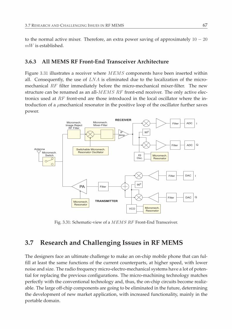
3.7 RESEARCH AND CHALLENGING ISSUES IN RF MEMS 67
to the normal active mixer. Therefore, an extra power saving of approximately 10 − 20
mW is established.
3.6.3 All MEMS RF Front-End Transceiver Architecture
Figure 3.31 illustrates a receiver where MEMS components have been inserted within
all. Consequently, the use of LNA is eliminated due to the localization of the micro-
mechanical RF filter immediately before the micro-mechanical mixer-filter. The new
structure can be renamed as an all-MEMS RF front-end receiver. The only active elec-
tronics used at RF front-end are those introduced in the local oscillator where the in-
troduction of a µmechanical resonator in the positive loop of the oscillator further saves
power.
Fig. 3.31: Schematic-view of a MEMS RF Front-End Transceiver.
3.7 Research and Challenging Issues in RF MEMS
The designers face an ultimate challenge to make an on-chip mobile phone that can ful-
fill at least the same functions of the current counterparts, at higher speed, with lower
noise and size. The radio frequency micro-electro-mechanical systems have a lot of poten-
tial for replacing the previous configurations. The micro-machining technology matches
perfectly with the conventional technology and, thus, the on-chip circuits become realiz-
able. The large off-chip components are going to be eliminated in the future, determining
the development of new market application, with increased functionality, mainly in the
portable domain.
68CHAPTER 3 MICRO-TECHNOLOGY EVOLUTION TOWARDS LARGE SCALE INTEGRATED RF MEMS
SYSTEMS
Wireless communication applications are dealing with new challenges in the field
of extra large carrier frequencies in order to provide good performances and accuracy.
Therefore, the on-going research deals with the replacement of off chip passive compo-
nents, as well as new all MEMS RF architectures while increasing the carrier frequency
up to many GHz. It is worth to noticing that the ultimate trend is to put more than tens
of micro-mechanical components on the same chip with CMOS circuits, for obtaining
more complex integrated electro-mechanical circuits that can function in the mentioned
environment. On the other hand, the devices realized in micro-machining technology
provide larger input and output impedances, making more difficult the realization of a
good match to antenna impedance. Hence, big effort is focusing on new solutions to
optimize the above issues.
3.8 Summary
This chapter consisted in a general overview on the state-of-the-art in micro-electro-mechanical
systems. The survey covered the most important high-Q RF MEMS vibrating devices
made in surface micro-machining technology and the functions fulfilled by them when
they are put together in emerging new RF architectures for wireless communication appli-
cations. The main target is to miniaturize and make possible the integration of the vibrat-
ing RF MEMS devices together with the CMOS technology on the same chip, to obtain
low power, low size, low noise requirements of the next generations of transceivers.
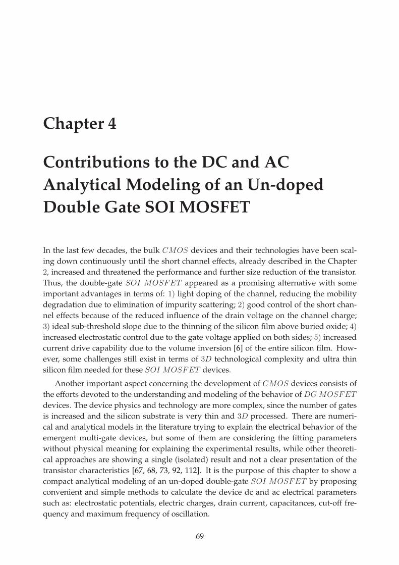
Chapter 4
Contributions to the DC and AC
Analytical Modeling of an Un-doped
Double Gate SOI MOSFET
In the last few decades, the bulk CMOS devices and their technologies have been scal-
ing down continuously until the short channel effects, already described in the Chapter
2, increased and threatened the performance and further size reduction of the transistor.
Thus, the double-gate SOI MOSFET appeared as a promising alternative with some
important advantages in terms of: 1) light doping of the channel, reducing the mobility
degradation due to elimination of impurity scattering; 2) good control of the short chan-
nel effects because of the reduced influence of the drain voltage on the channel charge;
3) ideal sub-threshold slope due to the thinning of the silicon film above buried oxide; 4)
increased electrostatic control due to the gate voltage applied on both sides; 5) increased
current drive capability due to the volume inversion [6] of the entire silicon film. How-
ever, some challenges still exist in terms of 3D technological complexity and ultra thin
silicon film needed for these SOI MOSFET devices.
Another important aspect concerning the development of CMOS devices consists of
the efforts devoted to the understanding and modeling of the behavior of DGMOSFET
devices. The device physics and technology are more complex, since the number of gates
is increased and the silicon substrate is very thin and 3D processed. There are numeri-
cal and analytical models in the literature trying to explain the electrical behavior of the
emergent multi-gate devices, but some of them are considering the fitting parameters
without physical meaning for explaining the experimental results, while other theoreti-
cal approaches are showing a single (isolated) result and not a clear presentation of the
transistor characteristics [67, 68, 73, 92, 112]. It is the purpose of this chapter to show a
compact analytical modeling of an un-doped double-gate SOI MOSFET by proposing
convenient and simple methods to calculate the device dc and ac electrical parameters
such as: electrostatic potentials, electric charges, drain current, capacitances, cut-off fre-
quency and maximum frequency of oscillation.
69
70CHAPTER 4 CONTRIBUTIONS TO THE DC AND AC ANALYTICAL MODELING OF AN UN-DOPED DOUBLE
GATE SOI MOSFET
In the beginning of the chapter, we are proposing simple mathematical methods needed
to perform a compact analytical model of the DC behavior of an Un-doped Double Gate
SOI MOSFET device. The main target is to explain theoretically the dc characteristics of
a symmetric transistor by calculating the silicon electrostatic potentials, inversion charge,
electrical current drain and the small-signal parameters in terms of transconductance and
output conductance. Besides, it is the purpose of this section to present detailed results
and the limitations of the one-dimensional analytical modeling of an un-doped asym-
metric DG SOI MOSFET . Finally, the AC analysis of an un-doped symmetric SOI
MOSFET device will be proposed by starting from the derivation of the small-signal
circuit, continuing with the evaluation of terminal charges and capacitances and ending
with the calculation of the RF figures of merits such as the cut-off frequency and the
maximum frequency of oscillation.
4.1 Contributions to the DC Analytical Modeling of a Sym-
metric Un-doped DG SOI MOSFET
4.1.1 Background of the DC Analysis for a Symmetric Un-doped DG
SOI MOSFET
For the first time, Y. Taur [111] has proposed the analytical calculation of Poisson’s equa-
tion in the silicon film of an un-doped symmetric DG SOI MOSFET , where only one
type of mobile charge (inversion charge) is present. Thus, he has solved the Poisson’s
equation, considering only the mobile electrons in the channel. According to it, Figure
4.1 shows an un-doped symmetric double gate SOI nMOSFET structure which will be
one-dimensional (1D) analytically analyzed, in this chapter. As it is depicted in the pic-
ture, the current flows only on the y direction, the one on the x direction being neglected.
As shown in this figure, the DG SOI MOSFET device presents the symmetry property,
according to which both gates have the same work function, oxide thickness and the same
applied voltage on the gate terminals.
The corresponding energy bands diagram of DG SOI nMOSFET is represented in
Figure 4.2. Because of the lack of contact in the silicon body of DG SOI MOSFET , the
Quasi-Fermi level is constant along the vertical direction (x axis) and the energy levels are
referred to the electron quasi-Fermi level of the n+ source/drain [112]. On the left side
(Figure 4.2a)), the energy bands diagram at thermodynamic equilibrium in the structure
is shown, while on the right side (Figure 4.2b)) the band bending in the presence of an
applied voltage on the gates is presented. In addition, this figure proves intuitively also
the volume inversion [6] specific to this DG SOI MOSFET , as due to the applied gate
voltage, the Fermi level is above the intrinsic Fermi level within the entire volume of an
initially p-type substrate.
The silicon thickness is thick enough so that the quantum confinement effects are not
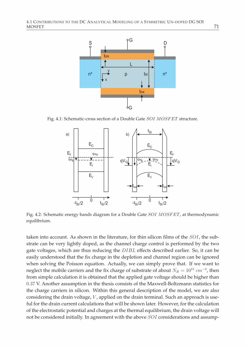
4.1 CONTRIBUTIONS TO THE DC ANALYTICAL MODELING OF A SYMMETRIC UN-DOPED DG SOIMOSFET 71
L
GDS
G
tsi
tox
x
y+n +n
tox
p
Fig. 4.1: Schematic-cross section of a Double Gate SOI MOSFET structure.
Fig. 4.2: Schematic energy bands diagram for a Double Gate SOI MOSFET , at thermodynamic
equilibrium.
taken into account. As shown in the literature, for thin silicon films of the SOI , the sub-
strate can be very lightly doped, as the channel charge control is performed by the two
gate voltages, which are thus reducing the DIBL effects described earlier. So, it can be
easily understood that the fix charge in the depletion and channel region can be ignored
when solving the Poisson equation. Actually, we can simply prove that. If we want to
neglect the mobile carriers and the fix charge of substrate of about NB = 1015 cm−3, then
from simple calculation it is obtained that the applied gate voltage should be higher than
0.37 V. Another assumption in the thesis consists of the Maxwell-Boltzmann statistics for
the charge carriers in silicon. Within this general description of the model, we are also
considering the drain voltage, V , applied on the drain terminal. Such an approach is use-
ful for the drain current calculations that will be shown later. However, for the calculation
of the electrostatic potential and charges at the thermal equilibrium, the drain voltage will
not be considered initially. In agreement with the above SOI considerations and assump-
72CHAPTER 4 CONTRIBUTIONS TO THE DC AND AC ANALYTICAL MODELING OF AN UN-DOPED DOUBLE
GATE SOI MOSFET
tions, the starting point of the analytical model consists of the calculation of the Poisson’s
equation as in [67, 73, 111] by using only the inversion charge, i.e., the electrons:
d2ψ
dx2=qni
εsi
· (e q(ψ−V )kT − e−
qψ
kT ) (4.1)
with the following boundary conditions:
dψ
dx|x=0 = 0 (4.2)
VGS − VFB = ψ|x=
tsi2
+εsitox
εox
· dψdx
|x=
tsi2
(4.3)
where: Ψ represents the electrostatic potential in the silicon body, VFB is the flat-band
voltage, VGS - gate to source voltage, tSi - silicon thickness, tox - oxide thickness (2nm
throughout the thesis), V is the channel voltage, when the VDS voltage is applied on the
device, εsi - electrical permittivity of the silicon, εox - electrical permittivity of the silicon
dioxide, k - Boltzmann constant, T - temperature, ni - intrinsic charge carrier concentra-
tion of silicon. Because we consider the mid-gap electrodes, the work function difference
between gate and silicon is zero, and for simplicity, we ignore the effect of the interface
charges on the flat-band voltage, and thus we take an ideal VFB = 0 V throughout the the-
sis. An alternative approach would be to operate everywhere in the thesis with VGS −VFB
as term instead of our VGS term.
The boundary condition (4.2) shows the idea of the maximum electrostatic potential
present in the central part of silicon film, while the boundary condition given by relation
(4.3) denotes the continuity of the normal electrical displacement at the interface between
silicon and SiO2.
From the first integration of Poisson’s equation, one can derive the electric field in the
silicon film:
dψ
dx=
√
2kTni
εsi
· e− qV
kT · [e qψkT − eqψ0kT ] (4.4)
and the electrostatic potential is computed by making the second integration of it:
ψ(x) = ψ0 −2kT
q· ln[cos(b · e
q(ψ0−V )2kT · x)] (4.5)
while the amount b is: b =√
q2ni2εsikT
and ψ0 represents the electrostatic potential at
the central point of the silicon body.
When x = ± tsi2
and by using the relation (4.5), the electrostatic potential at the silicon
film surface (ψs) is derived:
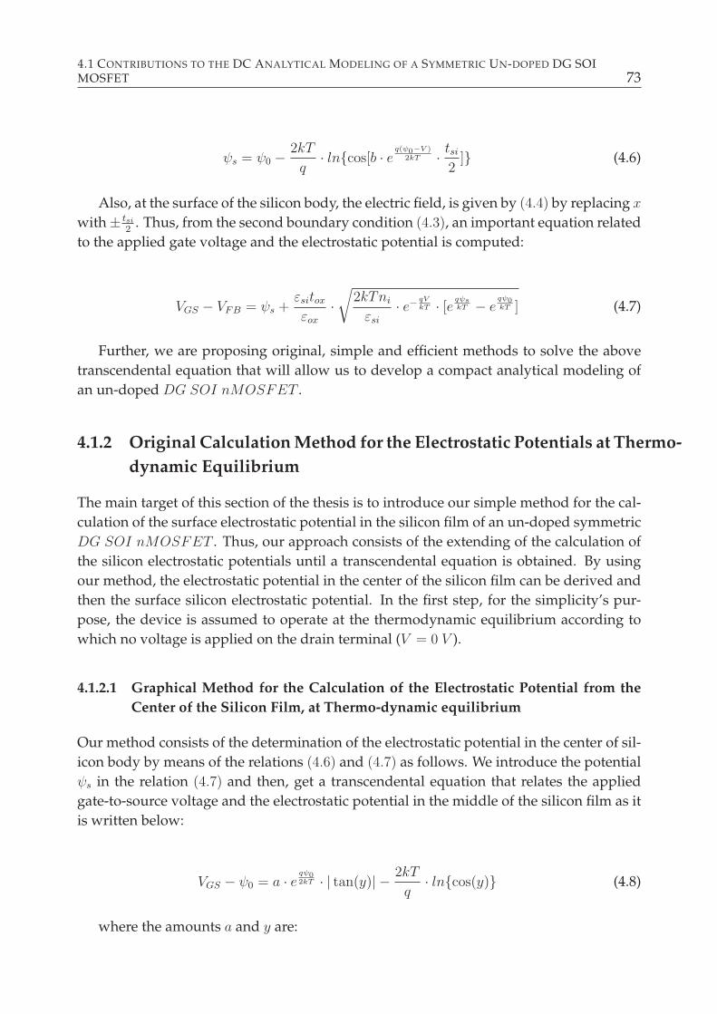
4.1 CONTRIBUTIONS TO THE DC ANALYTICAL MODELING OF A SYMMETRIC UN-DOPED DG SOIMOSFET 73
ψs = ψ0 −2kT
q· lncos[b · e
q(ψ0−V )2kT · tsi
2] (4.6)
Also, at the surface of the silicon body, the electric field, is given by (4.4) by replacing x
with ± tsi2
. Thus, from the second boundary condition (4.3), an important equation related
to the applied gate voltage and the electrostatic potential is computed:
VGS − VFB = ψs +εsitox
εox
·√
2kTni
εsi
· e− qV
kT · [e qψskT − eqψ0kT ] (4.7)
Further, we are proposing original, simple and efficient methods to solve the above
transcendental equation that will allow us to develop a compact analytical modeling of
an un-doped DG SOI nMOSFET .
4.1.2 Original Calculation Method for the Electrostatic Potentials at Thermo-
dynamic Equilibrium
The main target of this section of the thesis is to introduce our simple method for the cal-
culation of the surface electrostatic potential in the silicon film of an un-doped symmetric
DG SOI nMOSFET . Thus, our approach consists of the extending of the calculation of
the silicon electrostatic potentials until a transcendental equation is obtained. By using
our method, the electrostatic potential in the center of the silicon film can be derived and
then the surface silicon electrostatic potential. In the first step, for the simplicity’s pur-
pose, the device is assumed to operate at the thermodynamic equilibrium according to
which no voltage is applied on the drain terminal (V = 0 V ).
4.1.2.1 Graphical Method for the Calculation of the Electrostatic Potential from the
Center of the Silicon Film, at Thermo-dynamic equilibrium
Our method consists of the determination of the electrostatic potential in the center of sil-
icon body by means of the relations (4.6) and (4.7) as follows. We introduce the potential
ψs in the relation (4.7) and then, get a transcendental equation that relates the applied
gate-to-source voltage and the electrostatic potential in the middle of the silicon film as it
is written below:
VGS − ψ0 = a · eqψ02kT · | tan(y)| − 2kT
q· lncos(y) (4.8)
where the amounts a and y are:
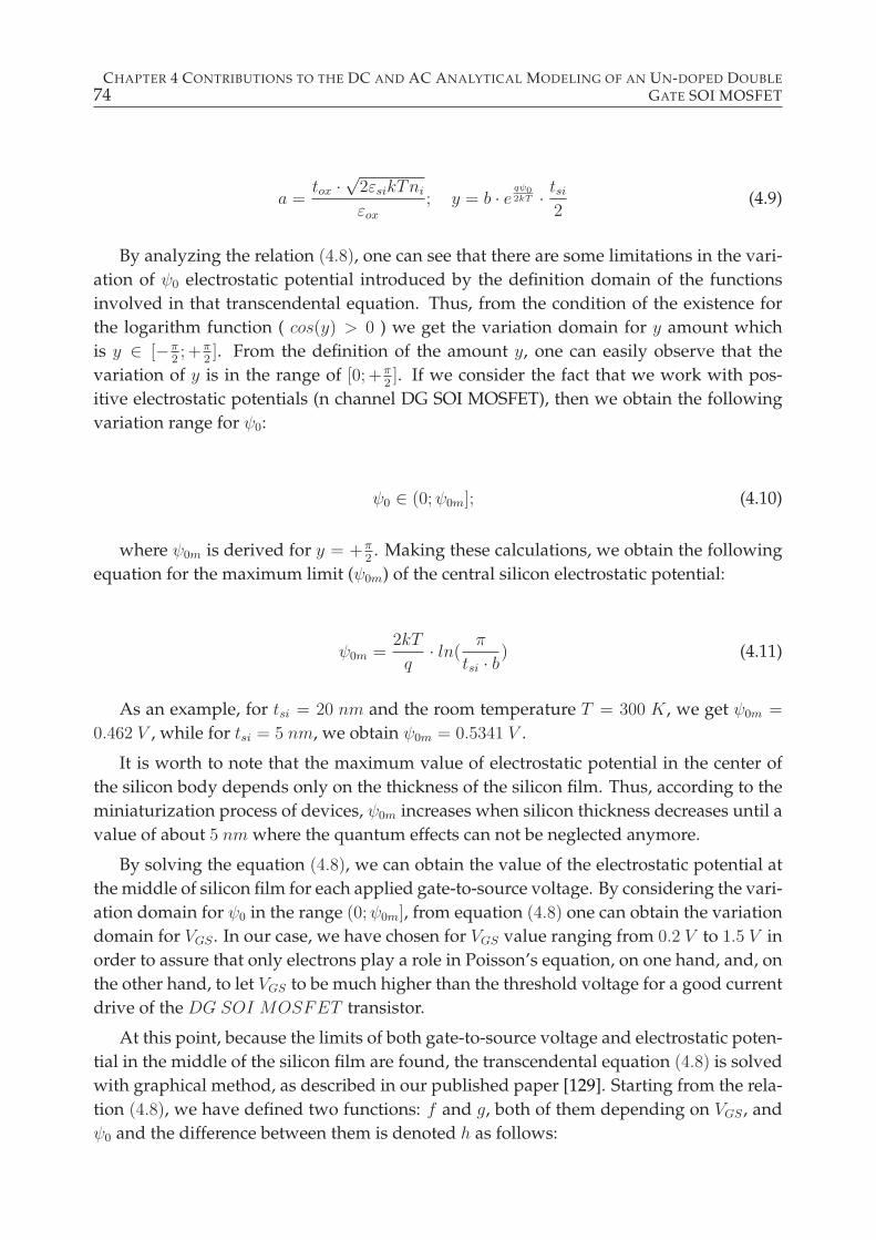
74CHAPTER 4 CONTRIBUTIONS TO THE DC AND AC ANALYTICAL MODELING OF AN UN-DOPED DOUBLE
GATE SOI MOSFET
a =tox ·
√2εsikTni
εox
; y = b · eqψ02kT · tsi
2(4.9)
By analyzing the relation (4.8), one can see that there are some limitations in the vari-
ation of ψ0 electrostatic potential introduced by the definition domain of the functions
involved in that transcendental equation. Thus, from the condition of the existence for
the logarithm function ( cos(y) > 0 ) we get the variation domain for y amount which
is y ∈ [−π2; +π
2]. From the definition of the amount y, one can easily observe that the
variation of y is in the range of [0; +π2]. If we consider the fact that we work with pos-
itive electrostatic potentials (n channel DG SOI MOSFET), then we obtain the following
variation range for ψ0:
ψ0 ∈ (0;ψ0m]; (4.10)
where ψ0m is derived for y = +π2. Making these calculations, we obtain the following
equation for the maximum limit (ψ0m) of the central silicon electrostatic potential:
ψ0m =2kT
q· ln(
π
tsi · b) (4.11)
As an example, for tsi = 20 nm and the room temperature T = 300 K, we get ψ0m =
0.462 V , while for tsi = 5 nm, we obtain ψ0m = 0.5341 V .
It is worth to note that the maximum value of electrostatic potential in the center of
the silicon body depends only on the thickness of the silicon film. Thus, according to the
miniaturization process of devices, ψ0m increases when silicon thickness decreases until a
value of about 5 nm where the quantum effects can not be neglected anymore.
By solving the equation (4.8), we can obtain the value of the electrostatic potential at
the middle of silicon film for each applied gate-to-source voltage. By considering the vari-
ation domain for ψ0 in the range (0;ψ0m], from equation (4.8) one can obtain the variation
domain for VGS . In our case, we have chosen for VGS value ranging from 0.2 V to 1.5 V in
order to assure that only electrons play a role in Poisson’s equation, on one hand, and, on
the other hand, to let VGS to be much higher than the threshold voltage for a good current
drive of the DG SOI MOSFET transistor.
At this point, because the limits of both gate-to-source voltage and electrostatic poten-
tial in the middle of the silicon film are found, the transcendental equation (4.8) is solved
with graphical method, as described in our published paper [129]. Starting from the rela-
tion (4.8), we have defined two functions: f and g, both of them depending on VGS , and
ψ0 and the difference between them is denoted h as follows:
4.1 CONTRIBUTIONS TO THE DC ANALYTICAL MODELING OF A SYMMETRIC UN-DOPED DG SOIMOSFET 75
f = VGS − ψ0 (4.12)
g = a · eqψ02kT · | tan(y)| − 2kT
q· lncos(y) (4.13)
h = f − g (4.14)
The definition domain of the two functions f and g is thoroughly analysed, so that to
be able to solve the above transcendental equation. For each value of VGS in the above
domain, ψ0 is allowed to vary from 0 to the ψ0max and, when h tends to zero, we obtain the
ψ0 corresponding to that input VGS value. The above described algorithm is implemented
in Matlab tool. In order to prove its efficiency and applicability, an example is given in
Figure 4.3, where the two functions f and g are represented in respect to ψ0 for VGS = 0.5
V , VFB = 0 V and VDS = 0 V . One can conclude that the intersection point of both
functions f and g represents the solution of the transcendental equation (4.8) or a given
set of values. Therefore, for an applied gate-to-source voltage of 0.5 V , a central silicon
electrostatic potential of 0.4353 V was obtained and this solution fits perfectly with the
condition introduced by (4.10).
0,0 0,1 0,2 0,3 0,4 0,5
0,0
0,1
0,2
0,3
0,4
0,5
0,6
Func
tions
f, g
Central Electrostatic Potential 0(V)
f g
VGS = 0.5 V
0.4353
Fig. 4.3: Graphical method for the calculation of the electrostatic potential drop in the center of the
silicon body ψ0, when VGS = 0.5 V . The functions f and g are dependent on ψ0 and VGS .
By using our method described above and varying the applied voltage on the gate
terminal, a range of solutions for the central silicon electrostatic potential is derived. Then
the electrostatic potential at the surface of the silicon film is obtained from relation (4.6).
Thus, we show in Figure 4.4 the dependence of ψ0 and ψs as a function of VGS for different
silicon thicknesses: 5 nm and 20 nm. The results for the electrostatic potential in the center
of the silicon film obtained with our graphical method in Matlab (see Appendix B.1) are
in good agreement with the results presented in the literature [112].
76CHAPTER 4 CONTRIBUTIONS TO THE DC AND AC ANALYTICAL MODELING OF AN UN-DOPED DOUBLE
GATE SOI MOSFET
0,0 0,2 0,4 0,6 0,8 1,0 1,2 1,4 1,60,15
0,20
0,25
0,30
0,35
0,40
0,45
0,50
0,55
0,60
0,65
Elec
trost
atic
Silic
on P
oten
tial
(V)
Gate to Source Voltage VGS [V]
0 for tSi = 20 nm
0 for tSi = 5 nm
s for tSi = 20 nm
s for tSi = 5 nm
Fig. 4.4: The electrostatic potentials ψs and ψ0 as a function of VGS voltage. This result was ob-
tained with our graphical method for silicon thickness of 5 nm and 20 nm.
4.1.3 Original Methods for the Calculation of the Electrostatic Poten-
tials at Thermodynamic Non-Equilibrium
An important step in the analytical modeling of the un-doped symmetricDGSOI MOSFET
has been done by S. Malobabic et.al. [73] where the influence of the applied voltage along
the channel on the mobile charge in the silicon film has been introduced. In their paper,
the Lambert function has been used for the calculation of the surface electrostatic poten-
tial in the silicon. Unfortunately, their approach is mathematically very complicated and
uses smoothing parameters without physical meaning. Therefore, this section is going to
introduce our two simple methods for the calculation of that surface electrostatic poten-
tial in the silicon film and, thus, making unnecessary the application of Lambert function
in a symmetrical DG SOI MOSFET device. The first approach is the above-mentioned
graphical method extended for different potentials applied on the drain terminal of the
transistor, while the second procedure relates with the bisection method used for the gen-
eral case of device’s operation, as described in our published paper [133].
4.1.3.1 Graphical Method for the Calculation of the Electrostatic Potential from the
Center of the Silicon Film
Within this subsection, for the calculation of the electrostatic potential at thermodynamic
non-equilibrium we extend our method presented before and in the paper [129], by in-
cluding the effects of the applied VDS voltage as shown below. From (4.3), (4.4) and (4.5),
the following transcendental equation is obtained:
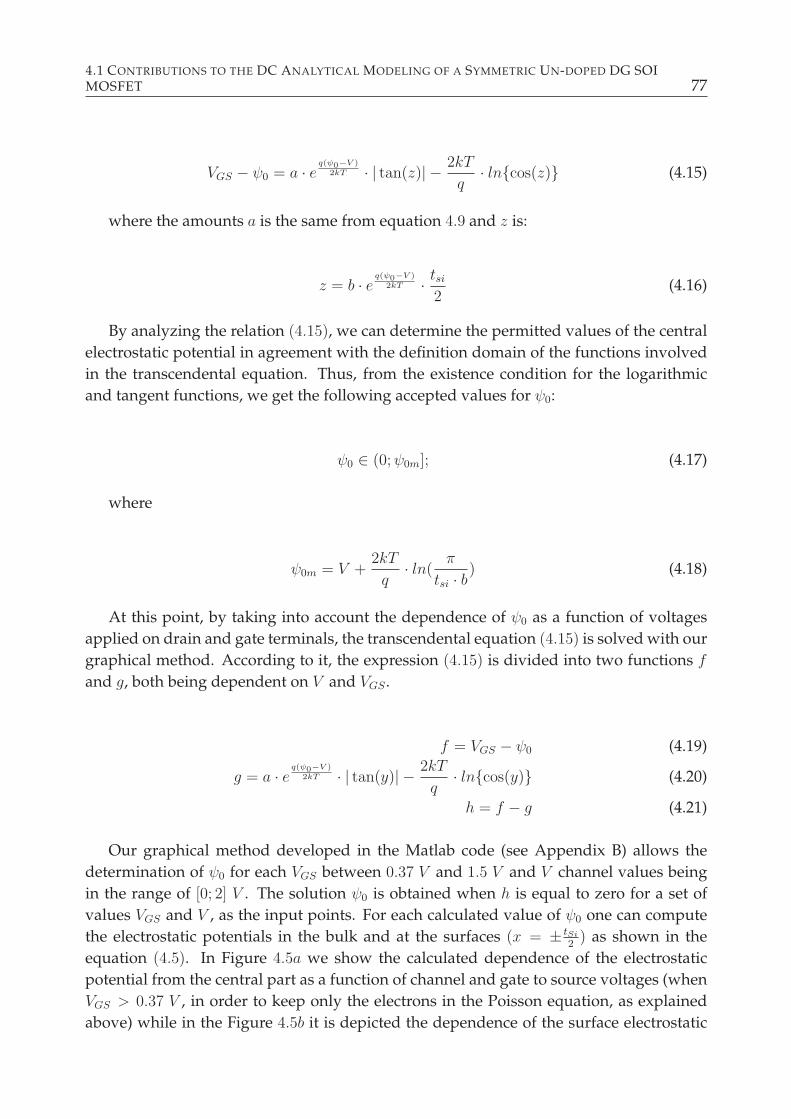
4.1 CONTRIBUTIONS TO THE DC ANALYTICAL MODELING OF A SYMMETRIC UN-DOPED DG SOIMOSFET 77
VGS − ψ0 = a · eq(ψ0−V )
2kT · | tan(z)| − 2kT
q· lncos(z) (4.15)
where the amounts a is the same from equation 4.9 and z is:
z = b · eq(ψ0−V )
2kT · tsi2
(4.16)
By analyzing the relation (4.15), we can determine the permitted values of the central
electrostatic potential in agreement with the definition domain of the functions involved
in the transcendental equation. Thus, from the existence condition for the logarithmic
and tangent functions, we get the following accepted values for ψ0:
ψ0 ∈ (0;ψ0m]; (4.17)
where
ψ0m = V +2kT
q· ln(
π
tsi · b) (4.18)
At this point, by taking into account the dependence of ψ0 as a function of voltages
applied on drain and gate terminals, the transcendental equation (4.15) is solved with our
graphical method. According to it, the expression (4.15) is divided into two functions f
and g, both being dependent on V and VGS .
f = VGS − ψ0 (4.19)
g = a · eq(ψ0−V )
2kT · | tan(y)| − 2kT
q· lncos(y) (4.20)
h = f − g (4.21)
Our graphical method developed in the Matlab code (see Appendix B) allows the
determination of ψ0 for each VGS between 0.37 V and 1.5 V and V channel values being
in the range of [0; 2] V . The solution ψ0 is obtained when h is equal to zero for a set of
values VGS and V , as the input points. For each calculated value of ψ0 one can compute
the electrostatic potentials in the bulk and at the surfaces (x = ± tSi2
) as shown in the
equation (4.5). In Figure 4.5a we show the calculated dependence of the electrostatic
potential from the central part as a function of channel and gate to source voltages (when
VGS > 0.37 V , in order to keep only the electrons in the Poisson equation, as explained
above) while in the Figure 4.5b it is depicted the dependence of the surface electrostatic
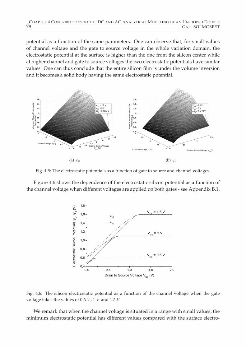
78CHAPTER 4 CONTRIBUTIONS TO THE DC AND AC ANALYTICAL MODELING OF AN UN-DOPED DOUBLE
GATE SOI MOSFET
potential as a function of the same parameters. One can observe that, for small values
of channel voltage and the gate to source voltage in the whole variation domain, the
electrostatic potential at the surface is higher than the one from the silicon center while
at higher channel and gate to source voltages the two electrostatic potentials have similar
values. One can thus conclude that the entire silicon film is under the volume inversion
and it becomes a solid body having the same electrostatic potential.
0.20.4
0.60.8
11.2
1.41.6
0
0.5
1
1.5
20.2
0.4
0.6
0.8
1
1.2
1.4
1.6
Gate to Source Voltage: V
GS (V)
Channel Voltage: V(V)
Min
imum
Sili
con E
lect
rost
atic
Pote
ntia
l (V
)
VGS
= 1.5 VV
DS = 0 V
psi0 = 0.4607 V
(a) ψ0
0
0.5
1
1.5
0
0.5
1
1.5
20.2
0.4
0.6
0.8
1
1.2
1.4
1.6
Gate to Source Voltage: VGS
(V)Channel Voltage: V (V)
Surf
ace
Sili
con E
lect
rost
atic
P
ote
ntia
l (V
)
VGS
= 1.5 VV
DS = 0 V
psi0 = 0.6173 V
(b) ψs
Fig. 4.5: The electrostatic potentials as a function of gate to source and channel voltages.
Figure 4.6 shows the dependence of the electrostatic silicon potential as a function of
the channel voltage when different voltages are applied on both gates - see Appendix B.1.
0,0 0,5 1,0 1,5 2,00,4
0,6
0,8
1,0
1,2
1,4
1,6
1,8
VGS = 1.5 V
VGS = 1 V
Elec
trost
atic
Silic
on P
oten
tials
0,
s (V)
Drain to Source Voltage VDS (V)
0
s
VGS = 0.5 V
Fig. 4.6: The silicon electrostatic potential as a function of the channel voltage when the gate
voltage takes the values of 0.5 V , 1 V and 1.5 V .
We remark that when the channel voltage is situated in a range with small values, the
minimum electrostatic potential has different values compared with the surface electro-
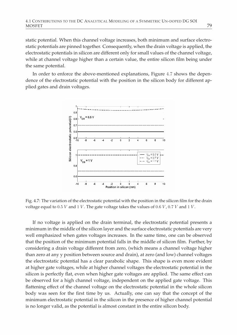
4.1 CONTRIBUTIONS TO THE DC ANALYTICAL MODELING OF A SYMMETRIC UN-DOPED DG SOIMOSFET 79
static potential. When this channel voltage increases, both minimum and surface electro-
static potentials are pinned together. Consequently, when the drain voltage is applied, the
electrostatic potentials in silicon are different only for small values of the channel voltage,
while at channel voltage higher than a certain value, the entire silicon film being under
the same potential.
In order to enforce the above-mentioned explanations, Figure 4.7 shows the depen-
dence of the electrostatic potential with the position in the silicon body for different ap-
plied gates and drain voltages.
Fig. 4.7: The variation of the electrostatic potential with the position in the silicon film for the drain
voltage equal to 0.5 V and 1 V . The gate voltage takes the values of 0.6 V , 0.7 V and 1 V .
If no voltage is applied on the drain terminal, the electrostatic potential presents a
minimum in the middle of the silicon layer and the surface electrostatic potentials are very
well emphasized when gates voltages increases. In the same time, one can be observed
that the position of the minimum potential falls in the middle of silicon film. Further, by
considering a drain voltage different from zero, (which means a channel voltage higher
than zero at any y position between source and drain), at zero (and low) channel voltages
the electrostatic potential has a clear parabolic shape. This shape is even more evident
at higher gate voltages, while at higher channel voltages the electrostatic potential in the
silicon is perfectly flat, even when higher gate voltages are applied. The same effect can
be observed for a high channel voltage, independent on the applied gate voltage. This
flattening effect of the channel voltage on the electrostatic potential in the whole silicon
body was seen for the first time by us. Actually, one can say that the concept of the
minimum electrostatic potential in the silicon in the presence of higher channel potential
is no longer valid, as the potential is almost constant in the entire silicon body.
80CHAPTER 4 CONTRIBUTIONS TO THE DC AND AC ANALYTICAL MODELING OF AN UN-DOPED DOUBLE
GATE SOI MOSFET
4.1.3.2 Bisection Method for the Calculation of the Electrostatic Potential from the
Center of the Silicon Film
Earlier, S. Malobabic et al. [73] has shown a method for solving the above transcendental
equation to obtain the values of ψ0 by using the Lambert function together with a set of
smoothing functions, as can be seen below.
ψ0 = U −√
U2 − (VGS − VFB) · VFB (4.22)
U =1
2· [(VGS − VFB) + (1 + r) · ψ0max] (4.23)
r = (Atox +B)(C
tsi+D)e−EV (4.24)
where the following parameters were found in order to model ψ0 from the above au-
thors: A = 0.0267 nm−1, B = 0.0270, C = 0.4526 nm, D = 0.0650, E = 3.2823 V −1, VFB = 0
V for simplicity, r is the shoulder smoothing parameter and equation (4.24) is empirical.
As the smoothing parameters have no physical meaning, we have developed a sim-
ple mathematical method for solving the same transcendental equation, as shown in our
published paper [133]. This is an alternative approach to our method presented above.
Thus, for the non-equilibrium conditions, our second proposed approach, the so-called
bisection method, solves a transcendental equation in which the surface electrostatic po-
tential is determined as a function of the gate-to-source voltage VGS and drain-to-source
voltage VDS as shown below.
When the relation (4.4) is introduced in (4.3), a transcendental equation is obtained
and then rearranged in order to have the following form:
ψS − VGS + a ·√
e−qV
kT
(
eqΨSkT − e
qψ0kT
)
= 0 (4.25)
The next step is to define a function, f , where its domain and co-domain are related
by the following expression:
f(ψS) = ψS − VGS + a ·√
e−qV
kT
(
eqΨSkT − e
qψ0kT
)
(4.26)
Now, one can easily remark that the solution of the equation (4.25) is obtained for
f(ψS) = 0, i.e., the solution is given by the intersection of the function f with the horizon-
tal axis, which is represented by ψS in this case. If the function keeps the same monotony
in a given interval [c, d] and goes through a zero value inside that interval, then the fol-
lowing condition f(c) ∗ f(d) < 0 is fulfilled.
In our case, the searched value of ψS must be in the range of [0, VGS], because the
electrostatic potential in the n-channel DG SOI MOSFET is positive and cannot exceed
the applied VGS voltage.
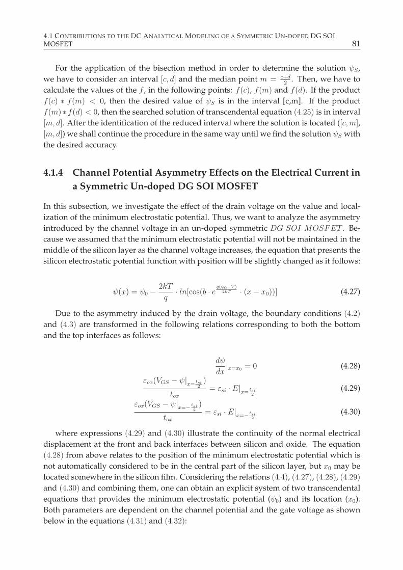
4.1 CONTRIBUTIONS TO THE DC ANALYTICAL MODELING OF A SYMMETRIC UN-DOPED DG SOIMOSFET 81
For the application of the bisection method in order to determine the solution ψS ,
we have to consider an interval [c, d] and the median point m = c+d2
. Then, we have to
calculate the values of the f , in the following points: f(c), f(m) and f(d). If the product
f(c) ∗ f(m) < 0, then the desired value of ψS is in the interval [c,m]. If the product
f(m)∗ f(d) < 0, then the searched solution of transcendental equation (4.25) is in interval
[m, d]. After the identification of the reduced interval where the solution is located ([c,m],
[m, d]) we shall continue the procedure in the same way until we find the solution ψS with
the desired accuracy.
4.1.4 Channel Potential Asymmetry Effects on the Electrical Current in
a Symmetric Un-doped DG SOI MOSFET
In this subsection, we investigate the effect of the drain voltage on the value and local-
ization of the minimum electrostatic potential. Thus, we want to analyze the asymmetry
introduced by the channel voltage in an un-doped symmetric DG SOI MOSFET . Be-
cause we assumed that the minimum electrostatic potential will not be maintained in the
middle of the silicon layer as the channel voltage increases, the equation that presents the
silicon electrostatic potential function with position will be slightly changed as it follows:
ψ(x) = ψ0 −2kT
q· ln[cos(b · e
q(ψ0−V )2kT · (x− x0))] (4.27)
Due to the asymmetry induced by the drain voltage, the boundary conditions (4.2)
and (4.3) are transformed in the following relations corresponding to both the bottom
and the top interfaces as follows:
dψ
dx|x=x0 = 0 (4.28)
εox(VGS − ψ|x=
tsi2
)
tox
= εsi · E|x=tsi2
(4.29)
εox(VGS − ψ|x=− tsi
2)
tox
= εsi · E|x=− tsi2
(4.30)
where expressions (4.29) and (4.30) illustrate the continuity of the normal electrical
displacement at the front and back interfaces between silicon and oxide. The equation
(4.28) from above relates to the position of the minimum electrostatic potential which is
not automatically considered to be in the central part of the silicon layer, but x0 may be
located somewhere in the silicon film. Considering the relations (4.4), (4.27), (4.28), (4.29)
and (4.30) and combining them, one can obtain an explicit system of two transcendental
equations that provides the minimum electrostatic potential (ψ0) and its location (x0).
Both parameters are dependent on the channel potential and the gate voltage as shown
below in the equations (4.31) and (4.32):
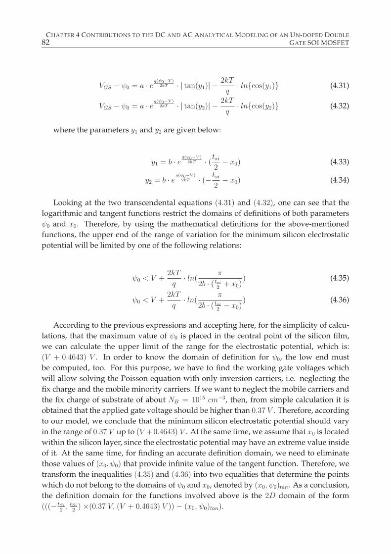
82CHAPTER 4 CONTRIBUTIONS TO THE DC AND AC ANALYTICAL MODELING OF AN UN-DOPED DOUBLE
GATE SOI MOSFET
VGS − ψ0 = a · eq(ψ0−V )
2kT · | tan(y1)| −2kT
q· lncos(y1) (4.31)
VGS − ψ0 = a · eq(ψ0−V )
2kT · | tan(y2)| −2kT
q· lncos(y2) (4.32)
where the parameters y1 and y2 are given below:
y1 = b · eq(ψ0−V )
2kT · (tsi2
− x0) (4.33)
y2 = b · eq(ψ0−V )
2kT · (−tsi2
− x0) (4.34)
Looking at the two transcendental equations (4.31) and (4.32), one can see that the
logarithmic and tangent functions restrict the domains of definitions of both parameters
ψ0 and x0. Therefore, by using the mathematical definitions for the above-mentioned
functions, the upper end of the range of variation for the minimum silicon electrostatic
potential will be limited by one of the following relations:
ψ0 < V +2kT
q· ln(
π
2b · ( tsi2
+ x0)) (4.35)
ψ0 < V +2kT
q· ln(
π
2b · ( tsi2− x0)
) (4.36)
According to the previous expressions and accepting here, for the simplicity of calcu-
lations, that the maximum value of ψ0 is placed in the central point of the silicon film,
we can calculate the upper limit of the range for the electrostatic potential, which is:
(V + 0.4643) V . In order to know the domain of definition for ψ0, the low end must
be computed, too. For this purpose, we have to find the working gate voltages which
will allow solving the Poisson equation with only inversion carriers, i.e. neglecting the
fix charge and the mobile minority carriers. If we want to neglect the mobile carriers and
the fix charge of substrate of about NB = 1015 cm−3, then, from simple calculation it is
obtained that the applied gate voltage should be higher than 0.37 V . Therefore, according
to our model, we conclude that the minimum silicon electrostatic potential should vary
in the range of 0.37 V up to (V +0.4643) V . At the same time, we assume that x0 is located
within the silicon layer, since the electrostatic potential may have an extreme value inside
of it. At the same time, for finding an accurate definition domain, we need to eliminate
those values of (x0, ψ0) that provide infinite value of the tangent function. Therefore, we
transform the inequalities (4.35) and (4.36) into two equalities that determine the points
which do not belong to the domains of ψ0 and x0, denoted by (x0, ψ0)tan. As a conclusion,
the definition domain for the functions involved above is the 2D domain of the form
(((− tSi2, tSi
2) ×(0.37 V, (V + 0.4643) V )) − (x0, ψ0)tan).
4.1 CONTRIBUTIONS TO THE DC ANALYTICAL MODELING OF A SYMMETRIC UN-DOPED DG SOIMOSFET 83
Now, after having obtained the definition intervals for each parameter, the graphical
method can be applied and the minimum electrostatic potential together (ψ0) with its po-
sition (x0) are calculated with transcendental equations (4.31) and (4.32) as it was shown
in our work [132]. For this, each relation is divided into two functions: f and g, both of
them being dependent on the channel voltage V and gate to source voltage VGS and the
difference between them is called h as it is shown below:
f1 = f2 = VGS − ψ0 (4.37)
g1 = a · eq(ψ0−V )
2kT · | tan(y1)| −2kT
q· lncos(y1) (4.38)
g2 = a · eq(ψ0−V )
2kT · | tan(y2)| −2kT
q· lncos(y2) (4.39)
h1 = f1 − g1 (4.40)
h2 = f2 − g2 (4.41)
For each value of VGS in the domain of [0; 1.5] V , ψ0 varies from 0.37 V up to V +0.4643
V while its position is allowed to move from − tSi2
up to tSi2
in both equations and, when h1
and h2 tend to zero, we obtain the ψ0 and x0 for that channel voltage. In this manner, we
calculate both minimum electrostatic potential and its position for the entire range. Figure
4.8 shows the dependence of the minimum, front surface and back surface electrostatic
potentials as a function of gate to source voltage for different channel voltages when the
silicon thickness equals to 10 nm and oxide thickness is 2 nm.
One can see that, for small channel voltages, the front and back surface potential de-
pendencies are split and the hypotheses with x0 different from zero makes sense. It is
worth to noticing, for high channel voltages, that the entire silicon layer has the same
electrostatic potential in each point of it. The result where the entire silicon body has
the same potential for high channel voltage was also obtained for the pure symmetric
approach, as described in the previous section.
In order to strongly emphasize, that an un-doped symmetric DG SOI MOSFET in-
troduces asymmetry effects, Figure 4.9 presents the variation of the silicon electrostatic
potentials with the channel voltage when the gate to source voltage equals to 0.6 V - see
the software program developed for this in the Appendix B.2.
Figure 4.10 depicts the distribution of the electrostatic potential in the silicon film
when the drain and gate voltages are those written in the graphics. We observe that the
position of the extremum is not in the central part of the silicon layer and the minimum is
shifting as a function of the applied channel voltages. When the drain voltage is different
from zero, one can notice that the shapes depend on the gate voltage and when those
channel voltages values are high enough, the overall silicon presents the same electro-
static potential. This figure also shows the difficulties in finding the minimum potential,
for higher values of channel voltage or gate voltage, when the dependence is almost flat
in the entire silicon body.
84CHAPTER 4 CONTRIBUTIONS TO THE DC AND AC ANALYTICAL MODELING OF AN UN-DOPED DOUBLE
GATE SOI MOSFET
Fig. 4.8: The silicon electrostatic potentials as a function of gate to source voltage VGS when the
channel potential has different values, for asymmetric DG SOI MOSFET transistor.
0,0 0,5 1,0 1,5 2,00,4
0,5
0,6
0,7
0,8
0,9
1,0
1,1
Sili
con
Ele
ctro
stat
ic P
oten
tials
0,
sf,
sb (V
)
Drain to Source Voltage VDS (V)
0
sf
sb
Fig. 4.9: The silicon electrostatic potentials as a function of channel voltage Vch when the gate to
source potential is 0.6 V .
Figure 4.11 depicts how the position of the minimum for the electrostatic potential is
shifted when a voltage is applied on the drain terminal.
Thus, despite of the symmetric property of the device, we observe a slight asymmetry
in its electrical characteristics introduced by the distribution of potential in the channel,
when a voltage is applied on the drain terminal. As a consequence of such phenomenon,
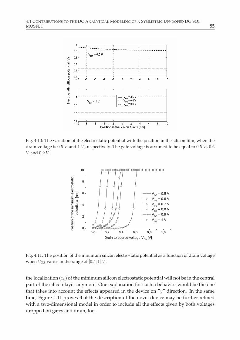
4.1 CONTRIBUTIONS TO THE DC ANALYTICAL MODELING OF A SYMMETRIC UN-DOPED DG SOIMOSFET 85
Fig. 4.10: The variation of the electrostatic potential with the position in the silicon film, when the
drain voltage is 0.5 V and 1 V , respectively. The gate voltage is assumed to be equal to 0.5 V , 0.6
V and 0.9 V .
0,0 0,2 0,4 0,6 0,8 1,00
2
4
6
8
10
Posi
tion
of th
e m
inim
um e
lect
rost
atic
po
tent
ial x
0 [nm
]
Drain to source voltage VDS [V]
VGS = 0.5 V VGS = 0.6 V VGS = 0.7 V VGS = 0.8 V VGS = 0.9 V VGS = 1 V
Fig. 4.11: The position of the minimum silicon electrostatic potential as a function of drain voltage
when VGS varies in the range of [0.5; 1] V .
the localization (x0) of the minimum silicon electrostatic potential will not be in the central
part of the silicon layer anymore. One explanation for such a behavior would be the one
that takes into account the effects appeared in the device on ”y” direction. In the same
time, Figure 4.11 proves that the description of the novel device may be further refined
with a two-dimensional model in order to include all the effects given by both voltages
dropped on gates and drain, too.
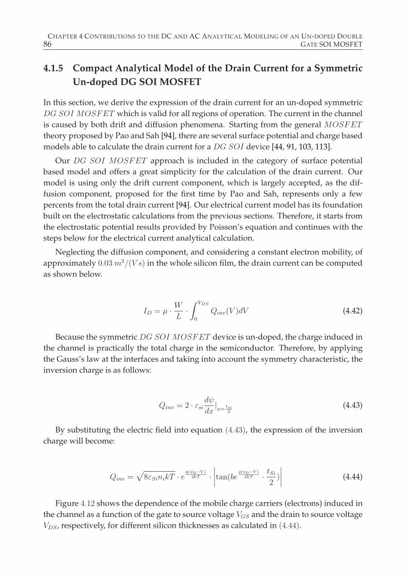
86CHAPTER 4 CONTRIBUTIONS TO THE DC AND AC ANALYTICAL MODELING OF AN UN-DOPED DOUBLE
GATE SOI MOSFET
4.1.5 Compact Analytical Model of the Drain Current for a Symmetric
Un-doped DG SOI MOSFET
In this section, we derive the expression of the drain current for an un-doped symmetric
DG SOI MOSFET which is valid for all regions of operation. The current in the channel
is caused by both drift and diffusion phenomena. Starting from the general MOSFET
theory proposed by Pao and Sah [94], there are several surface potential and charge based
models able to calculate the drain current for a DG SOI device [44, 91, 103, 113].
Our DG SOI MOSFET approach is included in the category of surface potential
based model and offers a great simplicity for the calculation of the drain current. Our
model is using only the drift current component, which is largely accepted, as the dif-
fusion component, proposed for the first time by Pao and Sah, represents only a few
percents from the total drain current [94]. Our electrical current model has its foundation
built on the electrostatic calculations from the previous sections. Therefore, it starts from
the electrostatic potential results provided by Poisson’s equation and continues with the
steps below for the electrical current analytical calculation.
Neglecting the diffusion component, and considering a constant electron mobility, of
approximately 0.03 m2/(V s) in the whole silicon film, the drain current can be computed
as shown below.
ID = µ · WL
·∫ VDS
0
Qinv(V )dV (4.42)
Because the symmetric DG SOI MOSFET device is un-doped, the charge induced in
the channel is practically the total charge in the semiconductor. Therefore, by applying
the Gauss’s law at the interfaces and taking into account the symmetry characteristic, the
inversion charge is as follows:
Qinv = 2 · εsi
dψ
dx|x=
tsi2
(4.43)
By substituting the electric field into equation (4.43), the expression of the inversion
charge will become:
Qinv =√
8εSinikT · eq(ψ0−V )
2kT ·∣
∣
∣
∣
tan(beq(ψ0−V )
2kT · tSi
2)
∣
∣
∣
∣
(4.44)
Figure 4.12 shows the dependence of the mobile charge carriers (electrons) induced in
the channel as a function of the gate to source voltage VGS and the drain to source voltage
VDS , respectively, for different silicon thicknesses as calculated in (4.44).
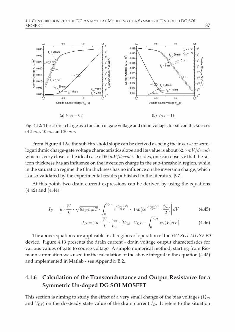
4.1 CONTRIBUTIONS TO THE DC ANALYTICAL MODELING OF A SYMMETRIC UN-DOPED DG SOIMOSFET 87
0,0 0,5 1,0 1,50,000
0,005
0,010
0,015
0,020
0,025
0,030
0,035
0,0 0,5 1,0 1,5
10-10
10-9
10-8
10-7
10-6
10-5
10-4
10-3
10-2
10-1
tSi = 20 nm
tSi = 5 nm
Carrier C
harge Q [C
/m2]C
arrie
r C
harg
e Q
[C/m
2 ]
Gate to Source Voltage VGS [V]
tox = 2 nm
tSi = 20 nm
tSi = 10 nm
tSi = 5 nm
VDS = 0 V
(a) VDS = 0V
0,0 0,5 1,0 1,5
0,000
0,002
0,004
0,006
0,008
0,010
0,012
0,014
0,016
0,018
0,0 0,5 1,0 1,5
10-18
10-16
10-14
10-12
10-10
10-8
10-6
10-4
10-2
Carrier C
harge Q [C
/m2]C
arrie
r C
harg
e Q
[C/m
2 ]
Drain to Source Voltage VDS [V]
tSi = 20 nm
tSi = 10 nm
tox = 2 nmVGS = 1 V
tSi = 5 nm
tSi = 20 nm
tSi = 10 nmtSi = 5 nm
(b) VGS = 1V
Fig. 4.12: The carrier charge as a function of gate voltage and drain voltage, for silicon thicknesses
of 5 nm, 10 nm and 20 nm.
From Figure 4.12a, the sub-threshold slope can be derived as being the inverse of semi-
logarithmic charge-gate voltage characteristics slope and its value is about 62.5mV/decade
which is very close to the ideal case of 60mV/decade. Besides, one can observe that the sil-
icon thickness has an influence on the inversion charge in the sub-threshold region, while
in the saturation regime the film thickness has no influence on the inversion charge, which
is also validated by the experimental results published in the literature [97].
At this point, two drain current expressions can be derived by using the equations
(4.42) and (4.44):
ID = µ · WL
·√
8εSinikT ·∫ VDS
0
eq(ψ0−V )
2kT ·∣
∣
∣
∣
tan(beq(ψ0−V )
2kT · tSi
2)
∣
∣
∣
∣
dV (4.45)
ID = 2µ · WL
· εox
tox
· [VGS · VDS −∫ VDS
0
ψs(V )dV ] (4.46)
The above equations are applicable in all regions of operation of theDGSOI MOSFET
device. Figure 4.13 presents the drain current - drain voltage output characteristics for
various values of gate to source voltage. A simple numerical method, starting from Rie-
mann summation was used for the calculation of the above integral in the equation (4.45)
and implemented in Matlab - see Appendix B.2.
4.1.6 Calculation of the Transconductance and Output Resistance for a
Symmetric Un-doped DG SOI MOSFET
This section is aiming to study the effect of a very small change of the bias voltages (VGS
and VDS) on the dc-steady state value of the drain current ID. It refers to the situation
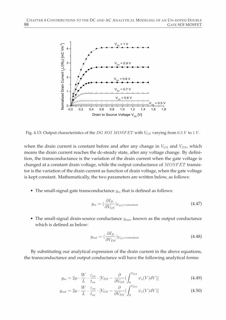
88CHAPTER 4 CONTRIBUTIONS TO THE DC AND AC ANALYTICAL MODELING OF AN UN-DOPED DOUBLE
GATE SOI MOSFET
0,0 0,2 0,4 0,6 0,8 1,0 1,2 1,4 1,6 1,80
1
2
3
4V
GS = 1 V
VGS
= 0.9 V
VGS
= 0.8 V
VGS
= 0.7 V
VGS
= 0.6 V
Nor
mal
ized
Dra
in C
urre
nt I D
L/(W
) [m
C V
m-2]
Drain to Source Voltage VDS [V]
VGS
= 0.5 V
Fig. 4.13: Output characteristics of the DG SOI MOSFET with VGS varying from 0.5 V to 1 V .
when the drain current is constant before and after any change in VGS and VDS , which
means the drain current reaches the dc-steady state, after any voltage change. By defini-
tion, the transconductance is the variation of the drain current when the gate voltage is
changed at a constant drain voltage, while the output conductance of MOSFET transis-
tor is the variation of the drain current as function of drain voltage, when the gate voltage
is kept constant. Mathematically, the two parameters are written below, as follows:
• The small-signal gate transconductance gm that is defined as follows:
gm = (∂ID∂VGS
)VDS=constant (4.47)
• The small-signal drain-source conductance gout, known as the output conductance
which is defined as below:
gout = (∂ID∂VDS
)VGS=constant (4.48)
By substituting our analytical expression of the drain current in the above equations,
the transconductance and output conductance will have the following analytical forms:
gm = 2µ · WL
· εox
tox
· [VDS − ∂
∂VGS
(
∫ VDS
0
ψs(V )dV )] (4.49)
gout = 2µ · WL
· εox
tox
· [VGS − ∂
∂VDS
(
∫ VDS
0
ψs(V )dV )] (4.50)
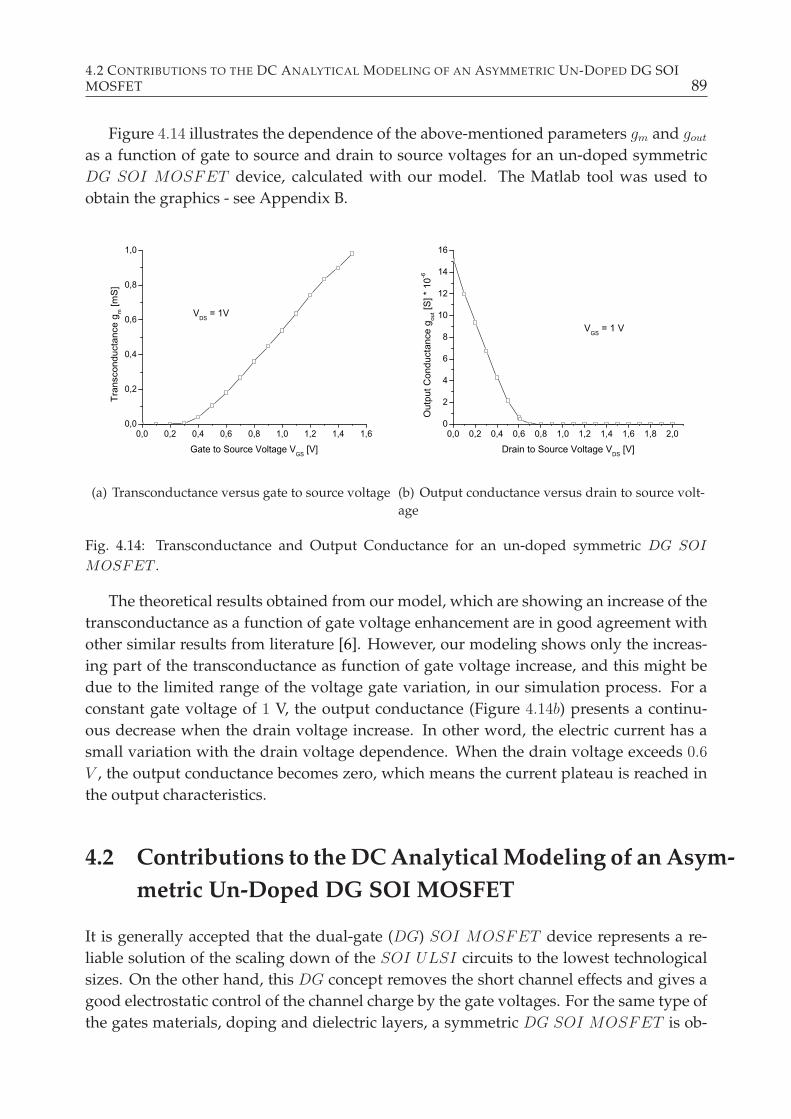
4.2 CONTRIBUTIONS TO THE DC ANALYTICAL MODELING OF AN ASYMMETRIC UN-DOPED DG SOIMOSFET 89
Figure 4.14 illustrates the dependence of the above-mentioned parameters gm and gout
as a function of gate to source and drain to source voltages for an un-doped symmetric
DG SOI MOSFET device, calculated with our model. The Matlab tool was used to
obtain the graphics - see Appendix B.
0,0 0,2 0,4 0,6 0,8 1,0 1,2 1,4 1,60,0
0,2
0,4
0,6
0,8
1,0
Tran
scon
duct
ance
gm [m
S]
Gate to Source Voltage VGS [V]
VDS = 1V
(a) Transconductance versus gate to source voltage
0,0 0,2 0,4 0,6 0,8 1,0 1,2 1,4 1,6 1,8 2,00
2
4
6
8
10
12
14
16
Out
put C
ondu
ctan
ce g
out [
S] *
10-6
Drain to Source Voltage VDS [V]
VGS = 1 V
(b) Output conductance versus drain to source volt-
age
Fig. 4.14: Transconductance and Output Conductance for an un-doped symmetric DG SOI
MOSFET .
The theoretical results obtained from our model, which are showing an increase of the
transconductance as a function of gate voltage enhancement are in good agreement with
other similar results from literature [6]. However, our modeling shows only the increas-
ing part of the transconductance as function of gate voltage increase, and this might be
due to the limited range of the voltage gate variation, in our simulation process. For a
constant gate voltage of 1 V, the output conductance (Figure 4.14b) presents a continu-
ous decrease when the drain voltage increase. In other word, the electric current has a
small variation with the drain voltage dependence. When the drain voltage exceeds 0.6
V , the output conductance becomes zero, which means the current plateau is reached in
the output characteristics.
4.2 Contributions to the DC Analytical Modeling of an Asym-
metric Un-Doped DG SOI MOSFET
It is generally accepted that the dual-gate (DG) SOI MOSFET device represents a re-
liable solution of the scaling down of the SOI ULSI circuits to the lowest technological
sizes. On the other hand, this DG concept removes the short channel effects and gives a
good electrostatic control of the channel charge by the gate voltages. For the same type of
the gates materials, doping and dielectric layers, a symmetric DG SOI MOSFET is ob-
90CHAPTER 4 CONTRIBUTIONS TO THE DC AND AC ANALYTICAL MODELING OF AN UN-DOPED DOUBLE
GATE SOI MOSFET
tained, while any technology differences at the gate and/or the dielectric level will imply
the asymmetry of the device. In the last years, 1D analytical modeling of both symmet-
ric and asymmetric DG SOI MOSFET has been used for the description of their DC
electrical behavior and the understanding of the device physics.
The analytical approach of the Poisson’s equation was possible by using only the in-
version charge and ignoring the fixed charge due to the lightly silicon doped film specific
to this DG SOI technology. One of the important results of the above modeling assump-
tions was the demonstration of the volume inversion in the ultra-thin silicon film of SOI
MOSFET devices. However, only a few modeling results were presented for the asym-
metric transistors, without the description of the used procedure and a clear presentation
of the validity domain. It is the purpose of our work to present detailed results and limi-
tations of the 1D analytical modeling of the asymmetric DG SOI MOSFET and to show
its differences compared to the symmetric case.
This section will present the background and the assumptions of the analytical mod-
eling, followed by our detailed mathematical approach which includes the identification
of the definition domain for the involved model parameters and the limitations of the
calculation of the electrostatic potential as a function of the applied VGS voltage.
4.2.1 Background of the 1D Analytical Modeling for an Asymmetric
DG SOI MOSFET
The analytical modeling will be related to the n-channel DG SOI MOSFET , where the
silicon thickness of the p-type silicon substrate (tSi) is equal to 20 nm, while the SiO2
gates dielectric thicknesses (tox) are equal to 2 nm. The geometry and the energy band
diagram of the asymmetric DG SOI MOSFET are presented in Figure 4.15, where one
can see that, due to the p and n type dopings of the two gates at the thermal equilibrium,
one silicon surface is already in inversion (see Figure 4.15a), while the other becomes
accumulated because of the differences in the work functions of gates materials and the
silicon substrate (see Figure 4.15b).
For lightly doped silicon film of the asymmetric DG SOI MOSFET , the analytical
approach was similar to the symmetrical case, where a minimum of the electrostatic po-
tential, ψ0, was assumed to be located in the silicon body, at the position x0, but not
exactly located in the center of the silicon layer as in the case of the symmetrical DG
SOI MOSFET . Thus, the calculation of the electrostatic potential was done by means of
Poisson’s equation and the specific boundary conditions as shown below:
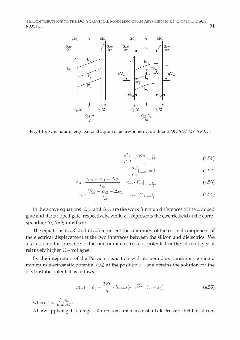
4.2 CONTRIBUTIONS TO THE DC ANALYTICAL MODELING OF AN ASYMMETRIC UN-DOPED DG SOIMOSFET 91
Fig. 4.15: Schematic energy bands diagram of an asymmetric, un-doped DG SOI MOSFET .
d2ψ
dx2=qni
εsi
· e qψkT (4.51)
dψ
dx|x=x0 = 0 (4.52)
εsi ·VGS − ψs1 − ∆φ1
tox
= εox · Esi|x=− tsi2
(4.53)
εsi ·VGS − ψs2 − ∆φ2
tox
= εox · Esi|x=tsi2
(4.54)
In the above equations, ∆φ1 and ∆φ2 are the work function differences of the n doped
gate and the p doped gate, respectively, while Esi represents the electric field at the corre-
sponding Si/SiO2 interfaces.
The equations (4.53) and (4.54) represent the continuity of the normal component of
the electrical displacement at the two interfaces between the silicon and dielectrics. We
also assume the presence of the minimum electrostatic potential in the silicon layer at
relatively higher VGS voltages.
By the integration of the Poisson’s equation with its boundary conditions giving a
minimum electrostatic potential (ψ0) at the position x0, one obtains the solution for the
electrostatic potential as follows:
ψ(x) = ψ0 −2kT
q· ln[cos(b · e
qψ02kT · (x− x0)] (4.55)
where b =√
q2ni2εsikT
.
At low applied gate voltages, Taur has assumed a constant electrostatic field in silicon,
92CHAPTER 4 CONTRIBUTIONS TO THE DC AND AC ANALYTICAL MODELING OF AN UN-DOPED DOUBLE
GATE SOI MOSFET
while at higher applied voltages a minimum electrostatic potential of 0.462V was found
and this was located near the center of the Si layer [112].
4.2.2 Clarifications and New Results of 1D Analytical modeling
An important limitation of 1D analytical modeling of the DG SOI MOSFET is given by
the use of only electron mobile inversion charge in the Poisson’s equation. This assump-
tion is valid for very low substrate doping and by neglecting the hole mobile charge.
In our case, for a better validation of the model assumption, we have used the p-type
substrate doping equal to NB = 1015 cm−3 which is a much lower value than the one de-
scribed in the literature. Based on our calculations [131], the electrostatic potentials higher
than 0.3 V will make negligible the influence of (mobile) holes and fixed depleted charge
in the above Poisson’s equation. For our NB value, the Fermi level is located below the
intrinsic Fermi level, Ei, and at 0.24 eV above Ev.
From the equations (4.53) and (4.54) and the dependence given by the relation (4.55),
we have derived the explicit system that provides the minimum electrostatic potential
(ψ0) and its location (x0) in silicon body:
VGS − ψ0 − ∆φ1 =
= −a · e qψ
2kT · tan(b · eqψ02kT · (−tsi
2− x0)) −
− 2kT
q· lncos(b · e
qψ02kT · (−tsi
2− x0)) (4.56)
VGS − ψ0 − ∆φ2 =
= −a · e qψ
2kT · tan(b · eqψ02kT · (tsi
2− x0)) −
− 2kT
q· lncos(b · e
qψ02kT · (tsi
2− x0)) (4.57)
where a = tox·√
2εsikTniεox
.
From the equations (4.56) and (4.57), one can see that the solutions ψ0 and x0 should
be in the definition domains of the natural logarithmic function and the tangent function.
Thus, the conditions for the existence of the logarithm function and tangent function are:
ψ0 <2kT
q· ln π
2b( tsi2
+ x0) (4.58)
ψ0 <2kT
q· ln π
2b( tsi2− x0)
(4.59)
From the relations (4.58) and (4.59), one can estimate an upper limit value of the min-
imum electrostatic potential (ψ0), by assuming the localization (x0) of this minimum in
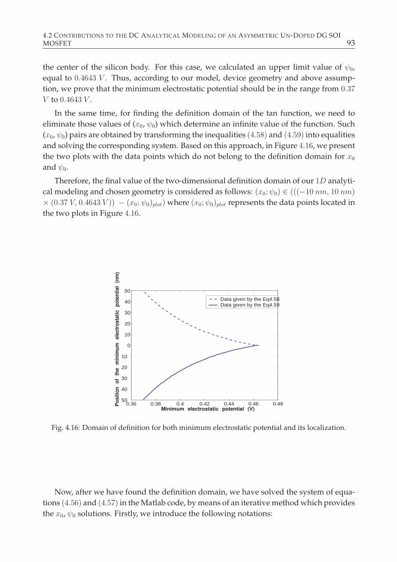
4.2 CONTRIBUTIONS TO THE DC ANALYTICAL MODELING OF AN ASYMMETRIC UN-DOPED DG SOIMOSFET 93
the center of the silicon body. For this case, we calculated an upper limit value of ψ0,
equal to 0.4643 V . Thus, according to our model, device geometry and above assump-
tion, we prove that the minimum electrostatic potential should be in the range from 0.37
V to 0.4643 V .
In the same time, for finding the definition domain of the tan function, we need to
eliminate those values of (x0, ψ0) which determine an infinite value of the function. Such
(x0, ψ0) pairs are obtained by transforming the inequalities (4.58) and (4.59) into equalities
and solving the corresponding system. Based on this approach, in Figure 4.16, we present
the two plots with the data points which do not belong to the definition domain for x0
and ψ0.
Therefore, the final value of the two-dimensional definition domain of our 1D analyti-
cal modeling and chosen geometry is considered as follows: (x0;ψ0) ∈ (((−10 nm, 10 nm)
× (0.37 V, 0.4643 V )) − (x0; ψ0)plot) where (x0;ψ0)plot represents the data points located in
the two plots in Figure 4.16.
0.36 0.38 0.4 0.42 0.44 0.46 0.4850
40
30
20
10
0
10
20
30
40
50
Minimum electrostatic potential (V)
Po
sit
ion
o
f th
e
min
imu
m
ele
ctr
os
tati
c
po
ten
tial
(nm
)
Data given by the Eq. 4.58Data given by the Eq. 4.59
Fig. 4.16: Domain of definition for both minimum electrostatic potential and its localization.
Now, after we have found the definition domain, we have solved the system of equa-
tions (4.56) and (4.57) in the Matlab code, by means of an iterative method which provides
the x0, ψ0 solutions. Firstly, we introduce the following notations:
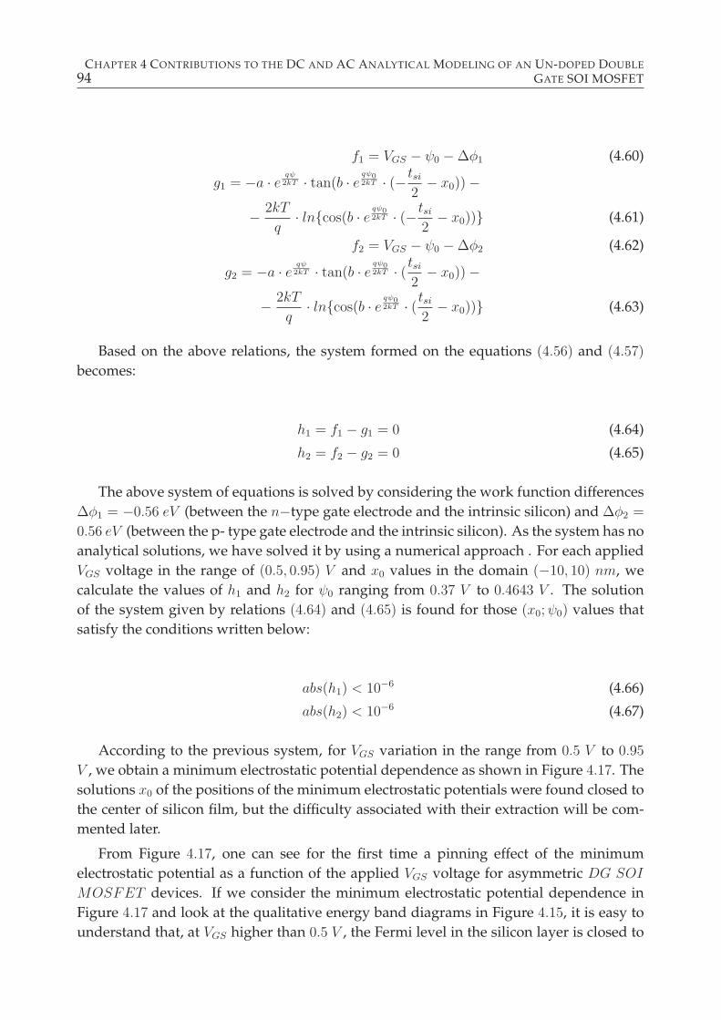
94CHAPTER 4 CONTRIBUTIONS TO THE DC AND AC ANALYTICAL MODELING OF AN UN-DOPED DOUBLE
GATE SOI MOSFET
f1 = VGS − ψ0 − ∆φ1 (4.60)
g1 = −a · e qψ
2kT · tan(b · eqψ02kT · (−tsi
2− x0)) −
− 2kT
q· lncos(b · e
qψ02kT · (−tsi
2− x0)) (4.61)
f2 = VGS − ψ0 − ∆φ2 (4.62)
g2 = −a · e qψ
2kT · tan(b · eqψ02kT · (tsi
2− x0)) −
− 2kT
q· lncos(b · e
qψ02kT · (tsi
2− x0)) (4.63)
Based on the above relations, the system formed on the equations (4.56) and (4.57)
becomes:
h1 = f1 − g1 = 0 (4.64)
h2 = f2 − g2 = 0 (4.65)
The above system of equations is solved by considering the work function differences
∆φ1 = −0.56 eV (between the n−type gate electrode and the intrinsic silicon) and ∆φ2 =
0.56 eV (between the p- type gate electrode and the intrinsic silicon). As the system has no
analytical solutions, we have solved it by using a numerical approach . For each applied
VGS voltage in the range of (0.5, 0.95) V and x0 values in the domain (−10, 10) nm, we
calculate the values of h1 and h2 for ψ0 ranging from 0.37 V to 0.4643 V . The solution
of the system given by relations (4.64) and (4.65) is found for those (x0;ψ0) values that
satisfy the conditions written below:
abs(h1) < 10−6 (4.66)
abs(h2) < 10−6 (4.67)
According to the previous system, for VGS variation in the range from 0.5 V to 0.95
V , we obtain a minimum electrostatic potential dependence as shown in Figure 4.17. The
solutions x0 of the positions of the minimum electrostatic potentials were found closed to
the center of silicon film, but the difficulty associated with their extraction will be com-
mented later.
From Figure 4.17, one can see for the first time a pinning effect of the minimum
electrostatic potential as a function of the applied VGS voltage for asymmetric DG SOI
MOSFET devices. If we consider the minimum electrostatic potential dependence in
Figure 4.17 and look at the qualitative energy band diagrams in Figure 4.15, it is easy to
understand that, at VGS higher than 0.5 V , the Fermi level in the silicon layer is closed to
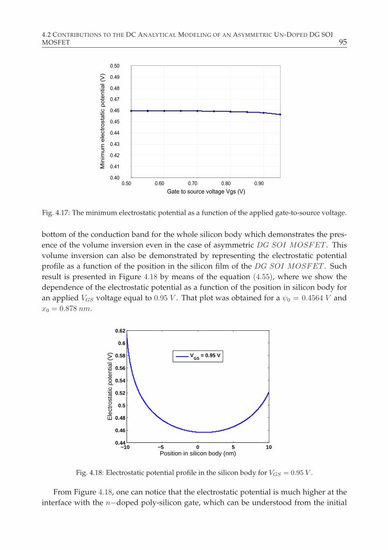
4.2 CONTRIBUTIONS TO THE DC ANALYTICAL MODELING OF AN ASYMMETRIC UN-DOPED DG SOIMOSFET 95
Fig. 4.17: The minimum electrostatic potential as a function of the applied gate-to-source voltage.
bottom of the conduction band for the whole silicon body which demonstrates the pres-
ence of the volume inversion even in the case of asymmetric DG SOI MOSFET . This
volume inversion can also be demonstrated by representing the electrostatic potential
profile as a function of the position in the silicon film of the DG SOI MOSFET . Such
result is presented in Figure 4.18 by means of the equation (4.55), where we show the
dependence of the electrostatic potential as a function of the position in silicon body for
an applied VGS voltage equal to 0.95 V . That plot was obtained for a ψ0 = 0.4564 V and
x0 = 0.878 nm.
−10 −5 0 5 100.44
0.46
0.48
0.5
0.52
0.54
0.56
0.58
0.6
0.62
Position in silicon body (nm)
Ele
ctro
stat
ic p
oten
tial (
V) V
GS = 0.95 V
Fig. 4.18: Electrostatic potential profile in the silicon body for VGS = 0.95 V .
From Figure 4.18, one can notice that the electrostatic potential is much higher at the
interface with the n−doped poly-silicon gate, which can be understood from the initial
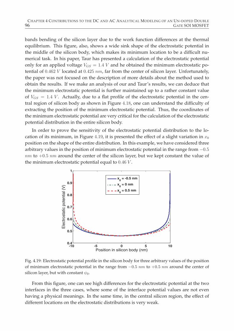
96CHAPTER 4 CONTRIBUTIONS TO THE DC AND AC ANALYTICAL MODELING OF AN UN-DOPED DOUBLE
GATE SOI MOSFET
bands bending of the silicon layer due to the work function differences at the thermal
equilibrium. This figure, also, shows a wide sink shape of the electrostatic potential in
the middle of the silicon body, which makes its minimum location to be a difficult nu-
merical task. In his paper, Taur has presented a calculation of the electrostatic potential
only for an applied voltage VGS = 1.4 V and he obtained the minimum electrostatic po-
tential of 0.462 V located at 0.425 nm, far from the center of silicon layer. Unfortunately,
the paper was not focused on the description of more details about the method used to
obtain the results. If we make an analysis of our and Taur’s results, we can deduce that
the minimum electrostatic potential is further maintained up to a rather constant value
of VGS = 1.4 V . Actually, due to a flat profile of the electrostatic potential in the cen-
tral region of silicon body as shown in Figure 4.18, one can understand the difficulty of
extracting the position of the minimum electrostatic potential. Thus, the coordinates of
the minimum electrostatic potential are very critical for the calculation of the electrostatic
potential distribution in the entire silicon body.
In order to prove the sensitivity of the electrostatic potential distribution to the lo-
cation of its minimum, in Figure 4.19, it is presented the effect of a slight variation in x0
position on the shape of the entire distribution. In this example, we have considered three
arbitrary values in the position of minimum electrostatic potential in the range from −0.5
nm to +0.5 nm around the center of the silicon layer, but we kept constant the value of
the minimum electrostatic potential equal to 0.46 V .
Fig. 4.19: Electrostatic potential profile in the silicon body for three arbitrary values of the position
of minimum electrostatic potential in the range from −0.5 nm to +0.5 nm around the center of
silicon layer, but with constant ψ0.
From this figure, one can see high differences for the electrostatic potential at the two
interfaces in the three cases, where some of the interface potential values are not even
having a physical meanings. In the same time, in the central silicon region, the effect of
different locations on the electrostatic distributions is very weak.
4.3 CONTRIBUTIONS TO THE AC ANALYSIS FOR A SYMMETRIC UN-DOPED DG SOI MOSFET 97
Overall, despite the sensitivity of the results to the accuracy of the numerical calcu-
lations, our approach has shown the capability of the 1D modeling to provide a good
understanding of the physics of the asymmetric DG SOI MOSFET devices, where the
volume inversion is found for a typical defined geometry and biasing.
4.3 Contributions to the AC Analysis for a Symmetric Un-
doped DG SOI MOSFET
In order to offer a comprehensive picture of the DG SOI MOSFET modeling, this sec-
tion deals with the description of our proposed ac analytical model, which is benefiting
from the quasi-static approximation up to an upper frequency limit of validity. Beyond
that upper frequency limit, non-quasi static models should be developed, but this is not
the goal of our thesis. Initially a large signal modeling is developed for the DG SOI
MOSFET transistor, adapted from the bulk MOSFET theory ( [115]) and then a small
signal modeling is shown, able to work for low and medium frequency range. Then, an
original equivalent small-signal circuit will be provided along with the calculation of the
device capacitances, making possible the theoretical study of the frequency response of
the asymmetric DG SOI MOSFET for understanding the frequency behavior of these
new emerging devices. Finally, a preliminary model for a small signal equivalent circuit
of a symmetric un-doped DG SOI MOSFET is derived considering the analytical mod-
eling results of the above novel MOSFET transistor that is going to continue the scaling
”race” beyond the bulk MOSFET technology capabilities.
4.3.1 The Large Signal Dynamic Modeling of a DG SOI MOSFET
Within this section, we shall start with our large signal dynamic modeling of the DG SOI
MOSFET , adapted after the bulk MOSFET theory. Here, at large ac signals, there will
be no restrictions about the magnitude of the dynamic signal superposed on the dc sig-
nal. The final goal of this section is to build an ac complete model used to provide the
equivalent small signal electric circuit for a symmetric un-doped DG SOI nMOSFET
device. This model should be able to describe the medium and high frequency operation
of the symmetric un-doped DG SOI nMOSFET device, as long as the approximation
of quasi-static operation is valid, as presented above. As known from the basic electron
device theory, at small ac signals, the magnitude of the dynamic excitation and response
is very small compared with dc bias, and the magnitude of the small signal (dynamic)
response is linear with respect to the small dynamic excitation. Here, the term complete
model refers to two aspects. Firstly, to obtain a complete model, the dc and low frequency
components are also included in the final equivalent circuit to describe the transport cur-
rent through transistor. As this is well known from the bulk MOSFET theory, here we
shall present the results without demonstration. Secondly, the dynamic effect of any ter-
98CHAPTER 4 CONTRIBUTIONS TO THE DC AND AC ANALYTICAL MODELING OF AN UN-DOPED DOUBLE
GATE SOI MOSFET
minal voltage variation to any terminal charge change and associated charging currents
is also incorporated in the DG SOI MOSFET model so that the resulting charging cur-
rents (specific only to dynamic regime of MOSFET transistors) will have corresponding
physical circuit elements for an enhanced validity of the ac model when compared with
experimental results. According to the quasi static approximation, even if the terminal
voltages are varying in time, the charges per unit area at any time are assumed identical
to those obtained if dc voltages are used instead. Consequently, the dc models for electric
charges and transport current are transferred to the ac regime modeling. This is the big
advantage of the quasi static approximation for modeling. However, as mentioned above,
one can not transfer any charging currents models from dc regime from the simple rea-
son that these charging currents do not exist, in the dc operation. The entire modeling
from here is considering only the intrinsic transistor (i.e, only the region of gate, dielectric
and inversion region from silicon are considered) ignoring the source and drain regions
and associated parasitic contributions, like series resistances and capacitances specific to
them.
We consider an intrinsic DG SOI MOSFET transistor with the total time varying
voltages that consist of a dc bias part and ac (dynamic) large signal part as follows:
vG1(t) = vg1(t) + VG1 (4.68)
vG2(t) = vg2(t) + VG2 (4.69)
vS(t) = vs(t) + VS (4.70)
vD(t) = vd(t) + VD (4.71)
In the above formulas, we do not put any restrictions on the magnitude of the ac
signal, as announced. The rules of capital and lowercase letters and subscripts are those
well known to the electronic circuit designers for total, ac and bias signals to be used for
dynamic modeling of circuits. In accordance to all the mentioned assumptions, Figure
4.20 presents an intrinsic asymmetric DG SOI nMOSFET transistor with four terminal
voltages consisting of a dc bias and a time varying signal. The schematics from Figure
4.20 will be used for either large and small signal modeling. For simplicity, in the above
figure we have introduced an original symbol for the asymmetric DG SOI nMOSFET
transistor, where we have shown the two separate biased gates and gate oxides, as well
as source, drain and silicon film of SOI . For the DG SOI nMOSFET transistor symbol,
we did not consider the BOX oxide and substrate effect, and its biasing. The floating
silicon film (p type in Figure 4.20), where the volume inversion can take place, is well
represented.
In addition, let us consider the currents ID, IG1, IS and IG2 defined as entering the
device. From the previous sections, we remember that the current flow is given by the
transport of electrons in the silicon (volume) inversion layer. Following the same steps
used in the conventional bulk MOSFET device, the transport current is defined as flow-
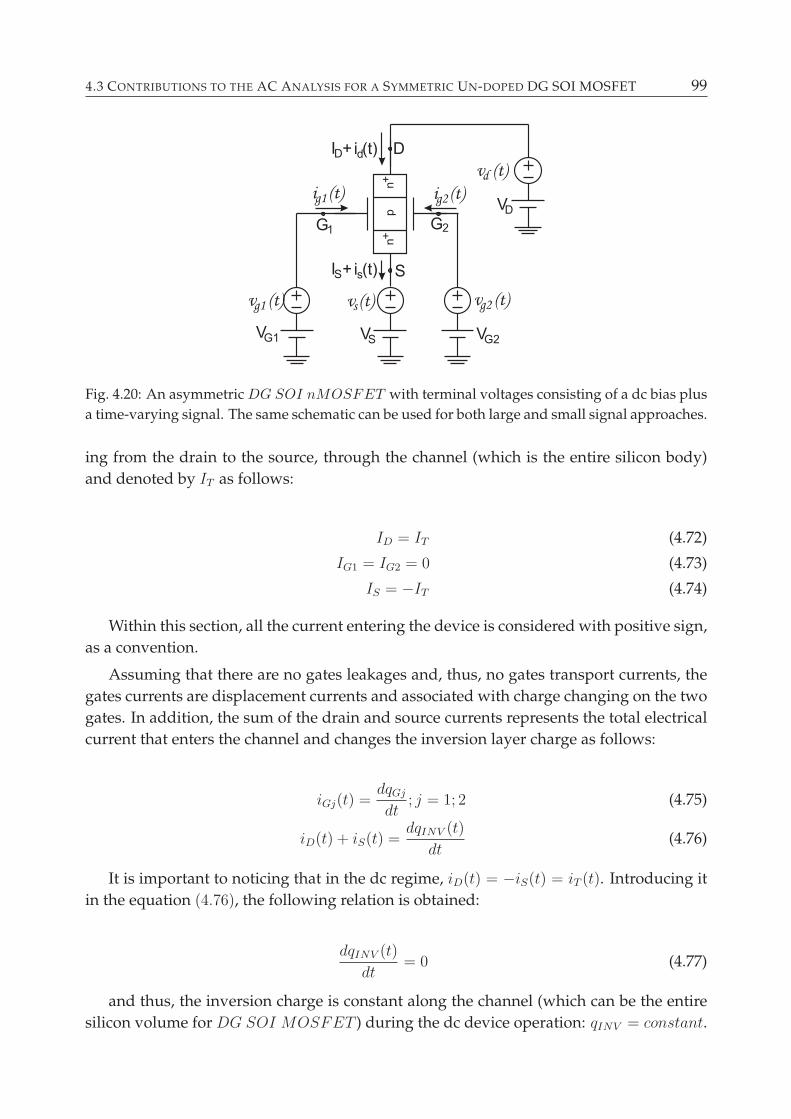
4.3 CONTRIBUTIONS TO THE AC ANALYSIS FOR A SYMMETRIC UN-DOPED DG SOI MOSFET 99
Fig. 4.20: An asymmetric DG SOI nMOSFET with terminal voltages consisting of a dc bias plus
a time-varying signal. The same schematic can be used for both large and small signal approaches.
ing from the drain to the source, through the channel (which is the entire silicon body)
and denoted by IT as follows:
ID = IT (4.72)
IG1 = IG2 = 0 (4.73)
IS = −IT (4.74)
Within this section, all the current entering the device is considered with positive sign,
as a convention.
Assuming that there are no gates leakages and, thus, no gates transport currents, the
gates currents are displacement currents and associated with charge changing on the two
gates. In addition, the sum of the drain and source currents represents the total electrical
current that enters the channel and changes the inversion layer charge as follows:
iGj(t) =dqGj
dt; j = 1; 2 (4.75)
iD(t) + iS(t) =dqINV (t)
dt(4.76)
It is important to noticing that in the dc regime, iD(t) = −iS(t) = iT (t). Introducing it
in the equation (4.76), the following relation is obtained:
dqINV (t)
dt= 0 (4.77)
and thus, the inversion charge is constant along the channel (which can be the entire
silicon volume for DG SOI MOSFET ) during the dc device operation: qINV = constant.
100CHAPTER 4 CONTRIBUTIONS TO THE DC AND AC ANALYTICAL MODELING OF AN UN-DOPED DOUBLE
GATE SOI MOSFET
If the voltages are time varying as it is in the ac regime, the charge becomes variable
(qinv 6= constant). Then, the first derivative in time of the total inversion charge is not zero
anymore and then, the sum of the drain current from the above definitions and equation
(4.76) is not zero providing a small difference between the source current (−iS(t)) and
drain current (−iD(t)) [115], as shown below.
dqinv(t)
dt6= 0 ⇒ id(t) 6= −iD(t) (4.78)
Therefore, it is assumed that in the general case of time-varying voltages, both drain
and source currents contain the transport current from dc regime, to which one adds an
ac component. In the literature, there was much confusion about dynamic modeling of
these ac drain and source currents. Now, as shown below, the things are clear and the
ac model is well understood after making the analogy of the dynamic MOS transistor
behavior with a dynamic fluid system consisting of two liquid tanks (source tank and
drain tank) communicating between them by a piston-controlled reservoir with variable
volume (corresponding to the inversion channel volume controlled by gate voltage). For
liquids, flowing in the tank system in the dc conditions, with the piston in a fix position,
the same amount of liquid per minute enters the source tank in the reservoir and then
flows away in the drain tank. This is exactly what happens to the MOS transistor at
dc regime, when drain and source currents are equal. When the valve piston is moved
down very fast and the reservoir is increasing its volume, a part of the liquid coming
from the source tank will remain ”stored” in the increased-volume reservoir, and during
a transient regime, the liquid flow entering the source tank will be higher than the liquid
flow arrived at drain tank (due to the additionally remained or ”stored” liquid in the
reservoir with increased volume), even if it is a serial system. This is exactly what happens
in the ac regime of MOS transistor, when the gate voltage is rapidly increased, and for
a short transient time, the drain current is decreasing with respect to the source current,
due to a kind of an additional ’stored’ charge in the inversion layer, associated to gate
voltage enhancement. With this dynamic fluid analogy in mind, now, it may be easier
to understand that in dynamic regime, the absolute value of source current cannot be
equal to the total drain current and that some charging currents (iSA(t) at source end and
iDA(t) at drain end) will appear for expressing this difference with respect to dc regime
(iT (t) = ID). These charging current components cannot be found in the dc regime. Those
total dynamic drain and source currents containing the dc transport current (expressed by
iT (t)) and the two charging currents iSA(t) and iDA(t) for source and drain, respectively,
as shown above, are written as mathematical expressions as follows.
iD(t) = iT (t) + iDA(t) (4.79)
iS(t) = −iT (t) + iDA(t) (4.80)
From these equations and (4.76), we get:
4.3 CONTRIBUTIONS TO THE AC ANALYSIS FOR A SYMMETRIC UN-DOPED DG SOI MOSFET 101
iDA(t) + iSA(t) =dqINV (t)
dt(4.81)
Therefore, one can conclude that the total transport current iT (t) is responsible for
the dc transport process, while the quantities iSA(t) and iDA(t) give the changing in the
inversion charge qINV (t), to comply with the total value of the gate voltage, specific to the
dynamic regime. It is obvious that for an increased value of gate voltage, in the dynamic
regime, an external observer can not distinguish any difference between the electrons
entering the source and charging the channel (like a reservoir with increased volume, due
to piston enlarging the volume of reservoir) and those leaving the drain, i.e., cannot make
a distinction between electrons contributing to charging current and transport current. By
introducing two dynamic fictitious charges from the source and the drain, to comply with
different values and mathematical expressions of the total source and drain currents, one
gets the following expression for the (large signal) total drain and source currents:
iDA(t) =dqDdt
(4.82)
iSA(t) =dqSdt
(4.83)
For example, if iDA(t) is negative, it means that the total drain current is smaller than
the transport value, due to the less charge flowing at the drain with respect to the dc
regime, when a change appears in the gate voltage, becoming higher for an nMOS tran-
sistor (”piston effect on the reservoir which will increase its volume”). From these expres-
sions, one can also see that, for the modeling purposes, we need to know only the first
derivative of the functions describing the fictitious charges from source and drain with
respect to time, and not the functions itself. The two functions expressing the sum of the
two fictitious charges have a constraint: the sum of the two fictitious charges should be
equal to the total inversion charge, as shown below.
By including the relations (4.82) and (4.83) in (4.81), one can obtain:
qD(t) + qS(t) = qINV (t) (4.84)
If the terminal voltages are varying very slow, the quasi-static operation is maintained
and, thus, the evaluation of the two quantities denoted by qS(t) and qD(t) in the dynamic
regime can be given as a function of the electrical potentials applied on the DG SOI
MOSFET , as modeled in the dc regime. The dc voltages are now replaced by the dc
value corresponding to the total voltage, as described in the equations (4.68) - (4.71). It
is worth to know, that, indeed, in the dc regime the sum of the two charge amounts
from above is equal to the total inversion charge, and therefore one can use the analytical
102CHAPTER 4 CONTRIBUTIONS TO THE DC AND AC ANALYTICAL MODELING OF AN UN-DOPED DOUBLE
GATE SOI MOSFET
expression already obtained in the dc modeling for the calculation of the qD and qS from
below:
qD(t) = fD(vD(t), vG1(t), vG2(t), vS(t)) (4.85)
qS(t) = fS(vD(t), vG1(t), vG2(t), vS(t)) (4.86)
where fS and fD represent functions that show the dependence of the qS and qD as
a function of the voltages applied on all four terminals of a DG SOI nMOSFET as it is
depicted in the Figure 4.20. Considering the device as a single node where all the electrical
currents are entering as presented in Figure 4.20, from Kirchhoff’s current law we get:
iD(t) + iG1(t) + iG2(t) + iS(t) = 0 (4.87)
It is important to note that the Kirchhoff’s current law holds also for the ac regime
where we have introduced the charging currents for source and drain, as shown above
and thus, the equation (4.87) becomes:
iDA(t) + iG1(t) + iG2(t) + iSA(t) = 0 (4.88)
By using the above equation, the following definitions for the current and capacitances
[115] and considering all the terminals of the device as voltage excitation points, we get
the following equations:
i(t) =dq
dt(4.89)
CKK =∂qK∂vK
|Q−point (4.90)
CKL = −∂qK∂vL
|Q−point;L 6= K (4.91)
and by having the general condition:
CKL 6= CLK (4.92)
the expressions for the small-signal charging currents (and thus explaining the small
letters for the electric currents from below) are derived as below:
4.3 CONTRIBUTIONS TO THE AC ANALYSIS FOR A SYMMETRIC UN-DOPED DG SOI MOSFET 103
iDA(t) = CDD · dvD
dt− CDS · dvS
dt− CDG1 ·
dvG1
dt− CDG2 ·
dvG2
dt(4.93)
iSA(t) = −CSD · dvD
dt+ CSS · dvS
dt− CSG1 ·
dvG1
dt− CSG2 ·
dvG2
dt(4.94)
iG1(t) = −CG1D · dvD
dt− CG1S · dvS
dt+ CG1G1 ·
dvG1
dt− CG1G2 ·
dvG2
dt(4.95)
iG2(t) = −CG2D · dvD
dt− CG2S · dvS
dt− CG2G1 ·
dvG1
dt+ CDG2 ·
dvG2
dt(4.96)
It does worth to noticing that the capacitance parameters used in the above equations
are not associated to the intrinsic physical capacitors at this moment, but simply quanti-
ties defined as in (4.90) and (4.91). For the theoretical calculation of the above charging
currents and capacitances, analytical functions for the charges should be known, and this
is the advantage of the quasi-static operation, that will allow us to ”import” them from
the dc models, under circumstances described previously. It is also worth to mention that
the above equations can define the right environment for the realization of the equivalent
small-signal circuit of the asymmetric and symmetric DG SOI nMOSFET . In the next
section, we shall describe what the electrical requirements are, for the transformation of
the above large signal equations into small signal equations.
4.3.2 The Small Signal Dynamic Modeling of a DG SOI MOSFET
According to the charging currents model described above for the dynamic regime of DG
SOI MOSFETS and the general theory of small signals applied in the electronic circuits,
one can admit that if the dc terminal voltages of DG SOI MOSFETS transistor are all
increased with small ac amounts, as in the equations (4.68) - (4.71), then the total currents
can be expressed as follows:
iT (t) = IT + it(t) (4.97)
iD(t) = iT (t) + iDA(t) = IT + it(t) + iDA(t) = IT (t) + it(t) + ida(t) = ID + id(t); (4.98)
as explained before, we have no dc component for iDA(t), being a charging current
specific only to the dynamic regime:
1. iS(t) = −iT (t) + iSA(t) = −(IT + it(t)) + iSA(t) = −IT − it(t) + isa(t) = IS + is(t)
(similarly, we have no dc component for iSA(t));
2. iG1(t) = ig1(t) (no dc gate current component as long as the gate oxide leakage is
almost zero);
3. iG2(t) = ig2(t) (no dc gate current component as long as the gate oxide leakage is
almost zero).
104CHAPTER 4 CONTRIBUTIONS TO THE DC AND AC ANALYTICAL MODELING OF AN UN-DOPED DOUBLE
GATE SOI MOSFET
In this environment, id(t), is(t), ig1(t), ig2(t) are all small signal current components.
From the above equations, we find the following relations for small signal current of the
drain and the source:
id(t) = it(t) + ida(t) = it(t) +dqddt
(4.99)
is(t) = −it(t) + isa(t) (4.100)
From the equation of small signal drain current, one can easily understand that for a
complete equivalent circuit, the circuit elements associated to the small-signal transport
current component (it(t)) specific to low frequency operation should be included in the
final circuit, as will be presented further. According to the definition of the small signal
regime, we have the following conditions that should be fulfilled:
id(t) << ID (4.101)
is(t) << IS (4.102)
The mentioned two conditions should be accomplished in the quasi-static regime
where the drain and source charge variations with time are slow enough, so that those
charging currents superpose to the small signal transport currents to remain much smaller
than the dc bias current for source and drain. Such a comment could help us to determine
the upper limit of the operation frequency where the quasi-static regime is still applicable.
In addition, specific for a small signal regime, it should remain the fact that, if we apply
small signal excitation voltages superposed to dc bias, the two current components we
obtain should be linear functions of the small signal excitation voltage.
Based on the above observations, the Kirchoff’s law of current becomes :
iDA(t) + iG1(t) + iG2(t) + iSA(t) = ida(t) + ig1(t) + ig2(t) + isa(t) (4.103)
Considering the presented approach of the small signal dynamic regime, the men-
tioned charging current expressions become:
ida(t) = Cdd ·dvd
dt− Cds ·
dvs
dt− Cdg1 ·
dvg1
dt− Cdg2 ·
dvg2
dt(4.104)
isa(t) = −Csd ·dvd
dt+ Css ·
dvs
dt− Csg1 ·
dvg1
dt− Csg2 ·
dvg2
dt(4.105)
ig1(t) = −Cg1d ·dvd
dt− Cg1s ·
dvs
dt+ Cg1g1 ·
dvg1
dt− Cg1g2 ·
dvg2
dt(4.106)
ig2(t) = −Cg2d ·dvd
dt− Cg2s ·
dvs
dt− Cg2g1 ·
dvg1
dt+ Cdg2 ·
dvg2
dt(4.107)
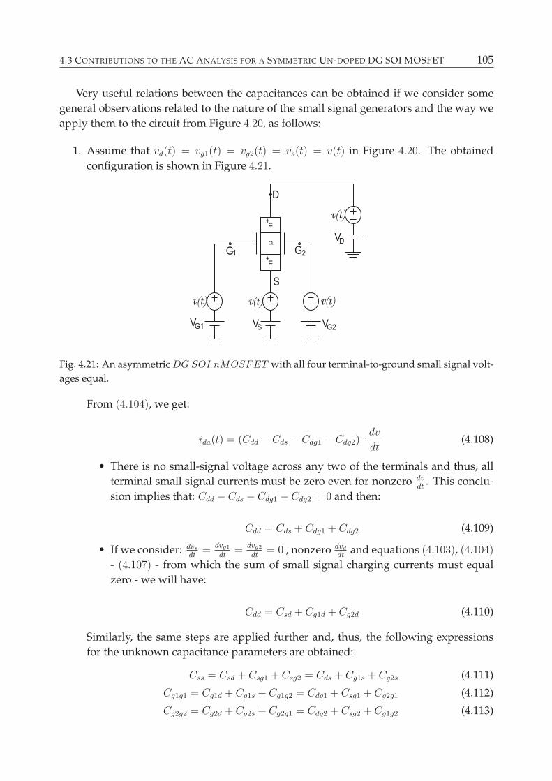
4.3 CONTRIBUTIONS TO THE AC ANALYSIS FOR A SYMMETRIC UN-DOPED DG SOI MOSFET 105
Very useful relations between the capacitances can be obtained if we consider some
general observations related to the nature of the small signal generators and the way we
apply them to the circuit from Figure 4.20, as follows:
1. Assume that vd(t) = vg1(t) = vg2(t) = vs(t) = v(t) in Figure 4.20. The obtained
configuration is shown in Figure 4.21.
Fig. 4.21: An asymmetricDG SOI nMOSFET with all four terminal-to-ground small signal volt-
ages equal.
From (4.104), we get:
ida(t) = (Cdd − Cds − Cdg1 − Cdg2) ·dv
dt(4.108)
• There is no small-signal voltage across any two of the terminals and thus, all
terminal small signal currents must be zero even for nonzero dvdt
. This conclu-
sion implies that: Cdd − Cds − Cdg1 − Cdg2 = 0 and then:
Cdd = Cds + Cdg1 + Cdg2 (4.109)
• If we consider: dvsdt
= dvg1dt
= dvg2dt
= 0 , nonzero dvddt
and equations (4.103), (4.104)
- (4.107) - from which the sum of small signal charging currents must equal
zero - we will have:
Cdd = Csd + Cg1d + Cg2d (4.110)
Similarly, the same steps are applied further and, thus, the following expressions
for the unknown capacitance parameters are obtained:
Css = Csd + Csg1 + Csg2 = Cds + Cg1s + Cg2s (4.111)
Cg1g1 = Cg1d + Cg1s + Cg1g2 = Cdg1 + Csg1 + Cg2g1 (4.112)
Cg2g2 = Cg2d + Cg2s + Cg2g1 = Cdg2 + Csg2 + Cg1g2 (4.113)
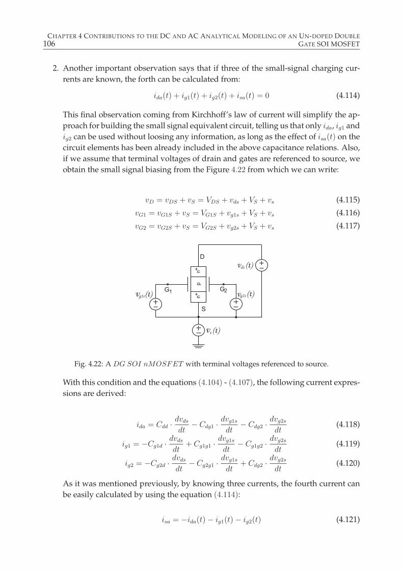
106CHAPTER 4 CONTRIBUTIONS TO THE DC AND AC ANALYTICAL MODELING OF AN UN-DOPED DOUBLE
GATE SOI MOSFET
2. Another important observation says that if three of the small-signal charging cur-
rents are known, the forth can be calculated from:
ida(t) + ig1(t) + ig2(t) + isa(t) = 0 (4.114)
This final observation coming from Kirchhoff’s law of current will simplify the ap-
proach for building the small signal equivalent circuit, telling us that only ida, ig1 and
ig2 can be used without loosing any information, as long as the effect of isa(t) on the
circuit elements has been already included in the above capacitance relations. Also,
if we assume that terminal voltages of drain and gates are referenced to source, we
obtain the small signal biasing from the Figure 4.22 from which we can write:
vD = vDS + vS = VDS + vds + VS + vs (4.115)
vG1 = vG1S + vS = VG1S + vg1s + VS + vs (4.116)
vG2 = vG2S + vS = VG2S + vg2s + VS + vs (4.117)
Fig. 4.22: A DG SOI nMOSFET with terminal voltages referenced to source.
With this condition and the equations (4.104) - (4.107), the following current expres-
sions are derived:
ida = Cdd ·dvds
dt− Cdg1 ·
dvg1s
dt− Cdg2 ·
dvg2s
dt(4.118)
ig1 = −Cg1d ·dvds
dt+ Cg1g1 ·
dvg1s
dt− Cg1g2 ·
dvg2s
dt(4.119)
ig2 = −Cg2d ·dvds
dt− Cg2g1 ·
dvg1s
dt+ Cdg2 ·
dvg2s
dt(4.120)
As it was mentioned previously, by knowing three currents, the fourth current can
be easily calculated by using the equation (4.114):
isa = −ida(t) − ig1(t) − ig2(t) (4.121)
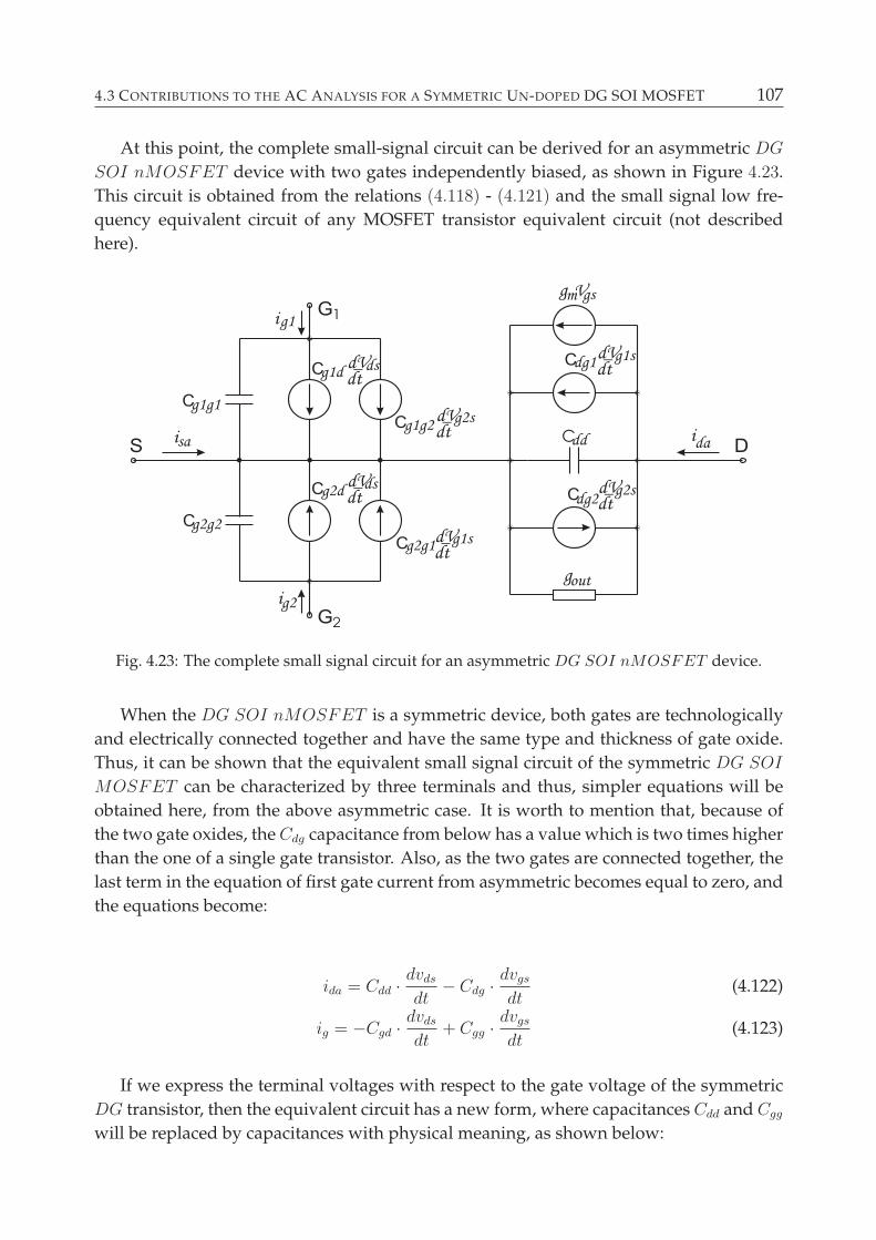
4.3 CONTRIBUTIONS TO THE AC ANALYSIS FOR A SYMMETRIC UN-DOPED DG SOI MOSFET 107
At this point, the complete small-signal circuit can be derived for an asymmetric DG
SOI nMOSFET device with two gates independently biased, as shown in Figure 4.23.
This circuit is obtained from the relations (4.118) - (4.121) and the small signal low fre-
quency equivalent circuit of any MOSFET transistor equivalent circuit (not described
here).
Fig. 4.23: The complete small signal circuit for an asymmetric DG SOI nMOSFET device.
When the DG SOI nMOSFET is a symmetric device, both gates are technologically
and electrically connected together and have the same type and thickness of gate oxide.
Thus, it can be shown that the equivalent small signal circuit of the symmetric DG SOI
MOSFET can be characterized by three terminals and thus, simpler equations will be
obtained here, from the above asymmetric case. It is worth to mention that, because of
the two gate oxides, theCdg capacitance from below has a value which is two times higher
than the one of a single gate transistor. Also, as the two gates are connected together, the
last term in the equation of first gate current from asymmetric becomes equal to zero, and
the equations become:
ida = Cdd ·dvds
dt− Cdg ·
dvgs
dt(4.122)
ig = −Cgd ·dvds
dt+ Cgg ·
dvgs
dt(4.123)
If we express the terminal voltages with respect to the gate voltage of the symmetric
DG transistor, then the equivalent circuit has a new form, where capacitances Cdd and Cgg
will be replaced by capacitances with physical meaning, as shown below:
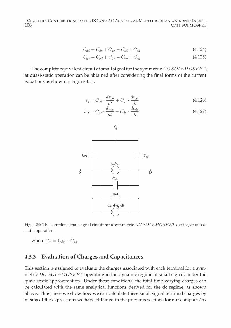
108CHAPTER 4 CONTRIBUTIONS TO THE DC AND AC ANALYTICAL MODELING OF AN UN-DOPED DOUBLE
GATE SOI MOSFET
Cdd = Cds + Cdg = Csd + Cgd (4.124)
Cgg = Cgd + Cgs = Cdg + Csg (4.125)
The complete equivalent circuit at small signal for the symmetricDGSOI nMOSFET ,
at quasi-static operation can be obtained after considering the final forms of the current
equations as shown in Figure 4.24.
ig = Cgd ·dvgd
dt+ Cgs ·
dvgs
dt(4.126)
ida = Cds ·dvds
dt+ Cdg ·
dvdg
dt(4.127)
Fig. 4.24: The complete small signal circuit for a symmetric DG SOI nMOSFET device, at quasi-
static operation.
where Cm = Cdg − Cgd.
4.3.3 Evaluation of Charges and Capacitances
This section is assigned to evaluate the charges associated with each terminal for a sym-
metric DG SOI nMOSFET operating in the dynamic regime at small signal, under the
quasi-static approximation. Under these conditions, the total time-varying charges can
be calculated with the same analytical functions derived for the dc regime, as shown
above. Thus, here we show how we can calculate these small signal terminal charges by
means of the expressions we have obtained in the previous sections for our compact DG
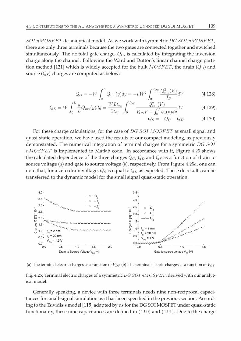
4.3 CONTRIBUTIONS TO THE AC ANALYSIS FOR A SYMMETRIC UN-DOPED DG SOI MOSFET 109
SOI nMOSFET dc analytical model. As we work with symmetric DG SOI nMOSFET ,
there are only three terminals because the two gates are connected together and switched
simultaneously. The dc total gate charge, QG, is calculated by integrating the inversion
charge along the channel. Following the Ward and Dutton’s linear channel charge parti-
tion method [121] which is widely accepted for the bulk MOSFET , the drain (QD) and
source (QS) charges are computed as below:
QG = −W∫ L
0
Qinv(y)dy = −µW 2
∫ VDS
0
Q2inv(V )
IDdV (4.128)
QD = W
∫ L
0
y
LQinv(y)dy =
WLtox
2ǫox
∫ VDS
0
Q2inv(V )
VGSV −∫ V
0ψs(v)dv
dV (4.129)
QS = −QG −QD (4.130)
For these charge calculations, for the case of DG SOI MOSFET at small signal and
quasi-static operation, we have used the results of our compact modeling, as previously
demonstrated. The numerical integration of terminal charges for a symmetric DG SOI
nMOSFET is implemented in Matlab code. In accordance with it, Figure 4.25 shows
the calculated dependence of the three charges QG, QD and QS as a function of drain to
source voltage (a) and gate to source voltage (b), respectively. From Figure 4.25a, one can
note that, for a zero drain voltage, QS is equal to QD as expected. These dc results can be
transferred to the dynamic model for the small signal quasi-static operation.
0.0 0.5 1.0 1.5 2.00.0
0.5
1.0
1.5
2.0
2.5
3.0
3.5
4.0
Cha
rges
Q [C
] * 1
014
Drain to Source Voltage VDS [v]
Qg
-Qs
-Qd
tox = 2 nmtSi = 20 nmVGS = 1.5 V
(a) The terminal electric charges as a function of VDS
0.0 0.5 1.0 1.50.0
0.5
1.0
1.5
2.0
2.5
3.0
3.5
Cha
rges
Q [C
] * 1
014
Gate to source voltage VGS [V]
Qg
Qs
Qd
tox = 2 nmtSi = 20 nmVDS = 1 V
(b) The terminal electric charges as a function of VGS
Fig. 4.25: Terminal electric charges of a symmetric DG SOI nMOSFET , derived with our analyt-
ical model.
Generally speaking, a device with three terminals needs nine non-reciprocal capaci-
tances for small-signal simulation as it has been specified in the previous section. Accord-
ing to the Tsividis’s model [115] adapted by us for the DG SOI MOSFET under quasi-static
functionality, these nine capacitances are defined in (4.90) and (4.91). Due to the charge
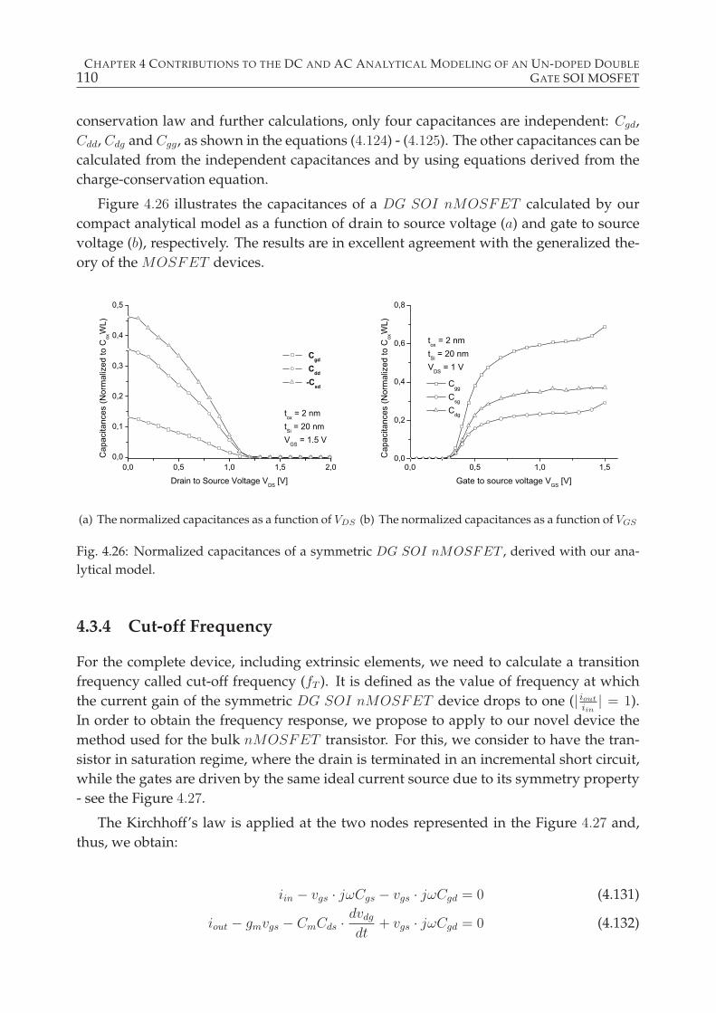
110CHAPTER 4 CONTRIBUTIONS TO THE DC AND AC ANALYTICAL MODELING OF AN UN-DOPED DOUBLE
GATE SOI MOSFET
conservation law and further calculations, only four capacitances are independent: Cgd,
Cdd, Cdg and Cgg, as shown in the equations (4.124) - (4.125). The other capacitances can be
calculated from the independent capacitances and by using equations derived from the
charge-conservation equation.
Figure 4.26 illustrates the capacitances of a DG SOI nMOSFET calculated by our
compact analytical model as a function of drain to source voltage (a) and gate to source
voltage (b), respectively. The results are in excellent agreement with the generalized the-
ory of the MOSFET devices.
0,0 0,5 1,0 1,5 2,00,0
0,1
0,2
0,3
0,4
0,5
Cap
acita
nces
(Nor
mal
ized
to C
oxW
L)
Drain to Source Voltage VDS [V]
Cgd
Cdd
-Csd
tox = 2 nmtSi = 20 nmVGS = 1.5 V
(a) The normalized capacitances as a function of VDS
0,0 0,5 1,0 1,50,0
0,2
0,4
0,6
0,8
Cap
acita
nces
(Nor
mal
ized
to C
oxW
L)
Gate to source voltage VGS [V]
Cgg
Csg
Cdg
tox = 2 nmtSi = 20 nmVDS = 1 V
(b) The normalized capacitances as a function of VGS
Fig. 4.26: Normalized capacitances of a symmetric DG SOI nMOSFET , derived with our ana-
lytical model.
4.3.4 Cut-off Frequency
For the complete device, including extrinsic elements, we need to calculate a transition
frequency called cut-off frequency (fT ). It is defined as the value of frequency at which
the current gain of the symmetric DG SOI nMOSFET device drops to one (| ioutiin
| = 1).
In order to obtain the frequency response, we propose to apply to our novel device the
method used for the bulk nMOSFET transistor. For this, we consider to have the tran-
sistor in saturation regime, where the drain is terminated in an incremental short circuit,
while the gates are driven by the same ideal current source due to its symmetry property
- see the Figure 4.27.
The Kirchhoff’s law is applied at the two nodes represented in the Figure 4.27 and,
thus, we obtain:
iin − vgs · jωCgs − vgs · jωCgd = 0 (4.131)
iout − gmvgs − CmCds ·dvdg
dt+ vgs · jωCgd = 0 (4.132)
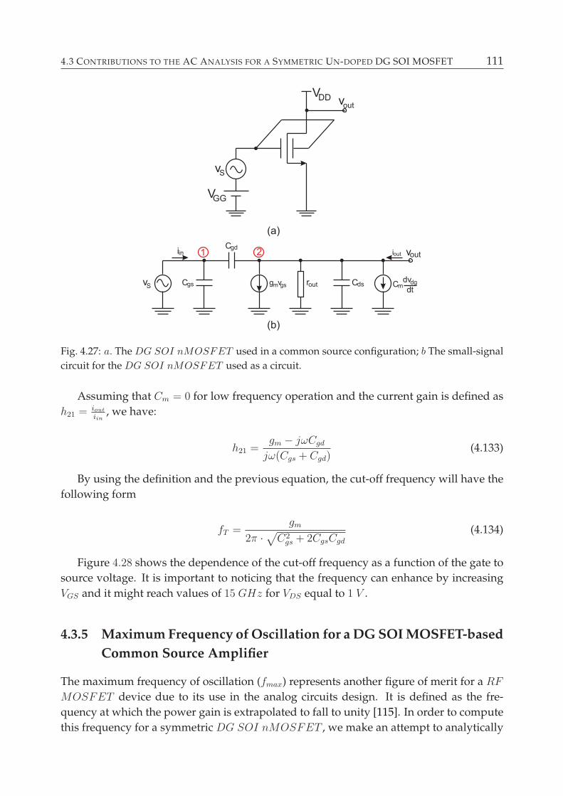
4.3 CONTRIBUTIONS TO THE AC ANALYSIS FOR A SYMMETRIC UN-DOPED DG SOI MOSFET 111
Fig. 4.27: a. The DG SOI nMOSFET used in a common source configuration; b The small-signal
circuit for the DG SOI nMOSFET used as a circuit.
Assuming that Cm = 0 for low frequency operation and the current gain is defined as
h21 = ioutiin
, we have:
h21 =gm − jωCgd
jω(Cgs + Cgd)(4.133)
By using the definition and the previous equation, the cut-off frequency will have the
following form
fT =gm
2π ·√
C2gs + 2CgsCgd
(4.134)
Figure 4.28 shows the dependence of the cut-off frequency as a function of the gate to
source voltage. It is important to noticing that the frequency can enhance by increasing
VGS and it might reach values of 15 GHz for VDS equal to 1 V .
4.3.5 Maximum Frequency of Oscillation for a DG SOI MOSFET-based
Common Source Amplifier
The maximum frequency of oscillation (fmax) represents another figure of merit for a RF
MOSFET device due to its use in the analog circuits design. It is defined as the fre-
quency at which the power gain is extrapolated to fall to unity [115]. In order to compute
this frequency for a symmetric DG SOI nMOSFET , we make an attempt to analytically
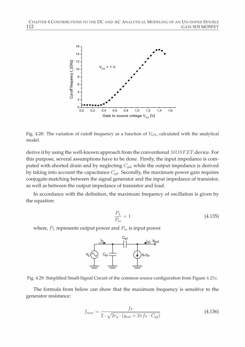
112CHAPTER 4 CONTRIBUTIONS TO THE DC AND AC ANALYTICAL MODELING OF AN UN-DOPED DOUBLE
GATE SOI MOSFET
0,0 0,2 0,4 0,6 0,8 1,0 1,2 1,4 1,60
2
4
6
8
10
12
14
16
Cut-o
ff fre
quen
cy f T [G
Hz]
Gate to source voltage VGS [V]
VDS = 1 V
Fig. 4.28: The variation of cutoff frequency as a function of VGS , calculated with the analytical
model.
derive it by using the well-known approach from the conventionalMOSFET device. For
this purpose, several assumptions have to be done. Firstly, the input impedance is com-
puted with shorted drain and by neglecting Cgd, while the output impedance is derived
by taking into account the capacitance Cgd. Secondly, the maximum power gain requires
conjugate-matching between the signal generator and the input impedance of transistor,
as well as between the output impedance of transistor and load.
In accordance with the definition, the maximum frequency of oscillation is given by
the equation:
PL
Pin
= 1 (4.135)
where, PL represents output power and Pin is input power.
Fig. 4.29: Simplified Small-Signal Circuit of the common source configuration from Figure 4.27a.
The formula from below can show that the maximum frequency is sensitive to the
generator resistance:
fmax =fT
2 ·√
2rg · (gout + 2πfT · Cgd)(4.136)
4.4 SUMMARY 113
4.4 Summary
The continuous scaling down of the channel length as well as the necessity of increas-
ing performances while short channel effects are maintained at the lowest level were the
driving force for the development of new devices based on silicon on insulator technol-
ogy. The so-called multiple-gate SOI MOSFETs are seen as one of the best possibilities
to replace the bulk MOSFET device, at the end of the road map. To receive large ac-
ceptance, simple and efficient static and dynamic models of the multi-gate SOI devices
should be developed and validated by experimental results. It has been the purpose of
this chapter to show our contribution to the analytical modeling of un-doped asymmetri-
cal and symmetrical DG SOI MOSFET devices in the static and dynamic regime.
An original, simple and efficient analytical approach has been proposed in this thesis
for the calculation of the electrostatic potential from the central part of the silicon layer in
the symmetric and asymmetric DG SOI MOSFET starting from the analytical approach
of Poisson’s equation. Then, the distribution of the electrostatic potential in the silicon
film was derived for both cases. Our procedure is based on mathematical computations
implemented in the Matlab code - see the Appendix B. Our method could replace other
complex approaches based on Lambert function and smoothing factor without physical
meaning which were previously used for the same electrostatic potential computation.
Continuing on the same direction, the electric inversion charge and drain current could be
calculated by using our analytical model in the symmetrical DG SOI MOSFET device,
in order to obtain a complete DC view.
Also, this chapter has shown the results and limits of a 1D analytical modeling for the
electrostatic potential distribution in the very slightly doped silicon body of the asym-
metric DG SOI MOSFET devices, where the asymmetry was given by the different p or
n type doping of the polysilicon gate electrodes. For the applied VGS voltages higher than
0.5V , the Poisson’s equation was analytically solved by using only the electrons as charge
carriers, the boundary conditions given by the continuity of the electric displacement at
the two interfaces and the presence of a minimum electrostatic potential in the silicon
body. The analytical approach was done in two steps. In the first step, the coordinates
of the minimum electrostatic potential were derived, while in the second step the electro-
static potential distribution was obtained. The analytical functions involved in the mod-
eling have restricted the coordinates of the minimum potential value to a well-defined 2D
existence domain. An iterative method performed in the Matlab code was used for the
calculation of the coordinates of the minimum electrostatic potential. At the end of this
process, we have demonstrated for the first time that, when the applied VGS voltage var-
ied from 0.5 V to 1 V , the minimum electrostatic potential was pinned at a value of about
0.459 V rather similar with the pinning phenomenon shown in the analytical modeling of
symmetric DG SOI MOSFET . The coordinates of the above minimum has allowed us
the calculation of the electrostatic potential distribution in the whole silicon body.
Despite the sensitivity of the electrostatic potential solution to the accuracy of its min-
114CHAPTER 4 CONTRIBUTIONS TO THE DC AND AC ANALYTICAL MODELING OF AN UN-DOPED DOUBLE
GATE SOI MOSFET
imum localization, our theoretical study described in this chapter has shown that the 1D
analytical modeling is a powerful tool to understand the physics of the asymmetric DG
SOI MOSFET devices and to prove a volume inversion for a typical geometry and bi-
asing.
In order to have a complete evaluation of a MOSFET device, it is necessary to offer
an AC view of it. Therefore, a small signal circuit for a symmetrical DG SOI MOSFET
has been proposed, starting from the assumption of the quasi-static operation. According
to it, even if the terminal voltages are varying in time, the charges per unit are assumed to
be identical at any time to those obtained if the dc voltages are used instead. In this envi-
ronment, the intrinsic small signal circuit has been constructed and the terminal charges
and capacitances were calculated by using the proposed analytical approach in order to
complete the AC description. At the end of the chapter, new models have been used to
compute the RF figures of merits in terms of the cut-off frequency and maximum fre-
quency of oscillation.
Chapter 5
Contributions to the Modeling and
Design of Circuits Based on DG SOI
MOSFET and MEMS
During the last few decades, the bulk MOSFET transistors have been continuously scal-
ing down, and today they are reaching deep sub-100 nm sizes, where the limitations due
to the short channel effects (SCE) are more and more challenging. This SCE threatening
has driven to a high demand for the development of new devices in silicon on insulator
technology such as double-gate SOI MOSFET . The IC designers have put a great effort
to investigate the potential of these novel devices for their use in the next generation of
digital and analog applications [55, 100]. Excellent analog performances of SOI devices in
terms of low leakage, high frequency operation, high voltage gain and transconductance
have been already electrically proven. However, the simulation of analog/digital circuits
based on multiple-gate SOI devices is still at the beginning since the existing compact
models for new transistors have not been accessible for market applications.
It is the purpose of this chapter to present a library created in Verilog A tool for the
compact analytical modeling of the symmetrical un-doped double-gate SOI MOSFET
given in Chapter 4 and to use this library for the design of circuits based on DG SOI
MOSFET devices. The main reason for using the Verilog A programming consists of its
incorporation within Cadence Virtuoso Design environment where the new device can
be further introduced in the structure of analog circuits. The chapter comprises of two
big parts. The first section of the chapter is assigned to the design of a common source
amplifier based on a DG SOI MOSFET transistor described with Verilog A tool. The
second section is proposing a procedure to design a configuration of future integrated
Colpitts oscillator consisting of a DG SOI MOSFET device and a RF MEMS resonator
as the positive feedback loop. The analytical behavioral model is based on an iterative
perturbation method, which is helping us to systematically analyze the transient and
steady state oscillations in the above-mentioned oscillator and finally, to design such a
novel circuit with a deep understanding of it.
115
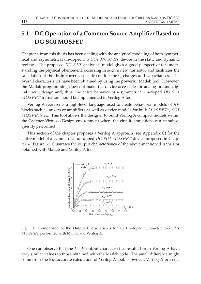
116CHAPTER 5 CONTRIBUTIONS TO THE MODELING AND DESIGN OF CIRCUITS BASED ON DG SOI
MOSFET AND MEMS
5.1 DC Operation of a Common Source Amplifier Based on
DG SOI MOSFET
Chapter 4 from this thesis has been dealing with the analytical modeling of both symmet-
rical and asymmetrical un-doped DG SOI MOSFET device in the static and dynamic
regimes. The proposed DG FET analytical model gives a good perspective for under-
standing the physical phenomena occurring in such a new transistor and facilitates the
calculation of the drain current, specific conductances, charges and capacitances. The
overall characteristics have been obtained by using the powerful Matlab tool. However,
the Matlab programming does not make the device accessible for analog or/and dig-
ital circuit design and, thus, the entire behavior of a symmetrical un-doped DG SOI
MOSFET transistor should be implemented in Verilog A tool.
Verilog A represents a high-level language used to create behavioral models of RF
blocks such as mixers or amplifiers as well as device models for bulk MOSFETs, SOI
MOSFETs etc. This tool allows the designer to build Verilog A compact models within
the Cadence Virtuoso Design environment where the circuit simulations can be subse-
quently performed.
This section of the chapter proposes a Verilog A approach (see Appendix C) for the
entire model of a symmetrical un-doped DG SOI MOSFET device proposed in Chap-
ter 4. Figure 5.1 illustrates the output characteristics of the above-mentioned transistor
obtained with Matlab and Verilog A tools.
0.0 0.2 0.4 0.6 0.8 1.0 1.2 1.4 1.60
1
2
3
4
VGS
= 1 V
VGS
= 0.9 V
VGS
= 0.8 V
VGS
= 0.7 V
VGS
= 0.6 V
Nor
mal
ized
dra
in c
urre
nt I D
L/(
W)
(mC
Vm
-2)
Drain to source voltage VDS
Verilog A Matlab
VGS
= 0.5 V
Fig. 5.1: Comparison of the Output Characteristics for an Un-doped Symmetric DG SOI
MOSFET performed with Matlab and Verilog A.
One can observe that the I − V output characteristics resulted from Verilog A have
very similar values to those obtained with the Matlab code. The small difference might
come from the less accurate calculation of Verilog A tool. However, Verilog A presents
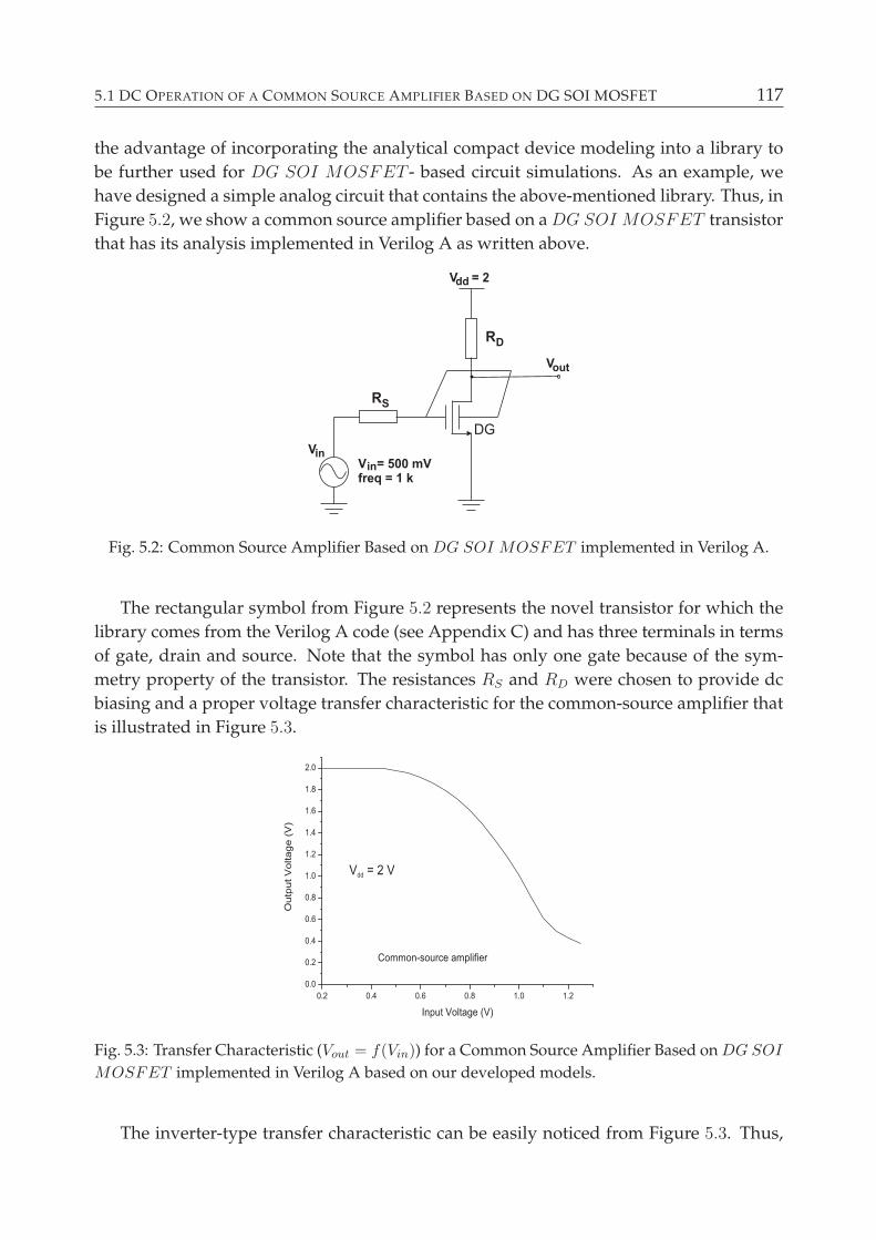
5.1 DC OPERATION OF A COMMON SOURCE AMPLIFIER BASED ON DG SOI MOSFET 117
the advantage of incorporating the analytical compact device modeling into a library to
be further used for DG SOI MOSFET - based circuit simulations. As an example, we
have designed a simple analog circuit that contains the above-mentioned library. Thus, in
Figure 5.2, we show a common source amplifier based on aDG SOI MOSFET transistor
that has its analysis implemented in Verilog A as written above.
Fig. 5.2: Common Source Amplifier Based on DG SOI MOSFET implemented in Verilog A.
The rectangular symbol from Figure 5.2 represents the novel transistor for which the
library comes from the Verilog A code (see Appendix C) and has three terminals in terms
of gate, drain and source. Note that the symbol has only one gate because of the sym-
metry property of the transistor. The resistances RS and RD were chosen to provide dc
biasing and a proper voltage transfer characteristic for the common-source amplifier that
is illustrated in Figure 5.3.
Fig. 5.3: Transfer Characteristic (Vout = f(Vin)) for a Common Source Amplifier Based onDG SOI
MOSFET implemented in Verilog A based on our developed models.
The inverter-type transfer characteristic can be easily noticed from Figure 5.3. Thus,
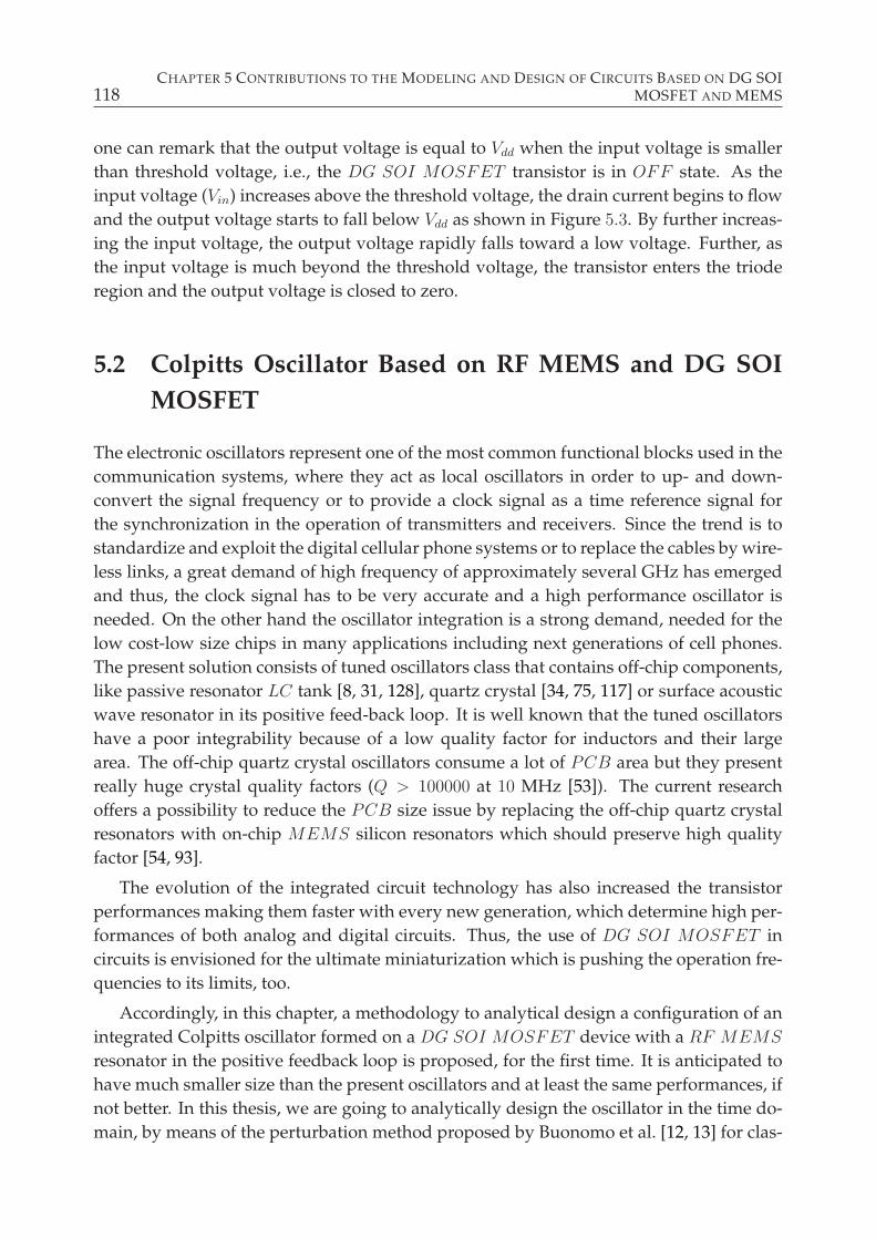
118CHAPTER 5 CONTRIBUTIONS TO THE MODELING AND DESIGN OF CIRCUITS BASED ON DG SOI
MOSFET AND MEMS
one can remark that the output voltage is equal to Vdd when the input voltage is smaller
than threshold voltage, i.e., the DG SOI MOSFET transistor is in OFF state. As the
input voltage (Vin) increases above the threshold voltage, the drain current begins to flow
and the output voltage starts to fall below Vdd as shown in Figure 5.3. By further increas-
ing the input voltage, the output voltage rapidly falls toward a low voltage. Further, as
the input voltage is much beyond the threshold voltage, the transistor enters the triode
region and the output voltage is closed to zero.
5.2 Colpitts Oscillator Based on RF MEMS and DG SOI
MOSFET
The electronic oscillators represent one of the most common functional blocks used in the
communication systems, where they act as local oscillators in order to up- and down-
convert the signal frequency or to provide a clock signal as a time reference signal for
the synchronization in the operation of transmitters and receivers. Since the trend is to
standardize and exploit the digital cellular phone systems or to replace the cables by wire-
less links, a great demand of high frequency of approximately several GHz has emerged
and thus, the clock signal has to be very accurate and a high performance oscillator is
needed. On the other hand the oscillator integration is a strong demand, needed for the
low cost-low size chips in many applications including next generations of cell phones.
The present solution consists of tuned oscillators class that contains off-chip components,
like passive resonator LC tank [8, 31, 128], quartz crystal [34, 75, 117] or surface acoustic
wave resonator in its positive feed-back loop. It is well known that the tuned oscillators
have a poor integrability because of a low quality factor for inductors and their large
area. The off-chip quartz crystal oscillators consume a lot of PCB area but they present
really huge crystal quality factors (Q > 100000 at 10 MHz [53]). The current research
offers a possibility to reduce the PCB size issue by replacing the off-chip quartz crystal
resonators with on-chip MEMS silicon resonators which should preserve high quality
factor [54, 93].
The evolution of the integrated circuit technology has also increased the transistor
performances making them faster with every new generation, which determine high per-
formances of both analog and digital circuits. Thus, the use of DG SOI MOSFET in
circuits is envisioned for the ultimate miniaturization which is pushing the operation fre-
quencies to its limits, too.
Accordingly, in this chapter, a methodology to analytical design a configuration of an
integrated Colpitts oscillator formed on a DG SOI MOSFET device with a RF MEMS
resonator in the positive feedback loop is proposed, for the first time. It is anticipated to
have much smaller size than the present oscillators and at least the same performances, if
not better. In this thesis, we are going to analytically design the oscillator in the time do-
main, by means of the perturbation method proposed by Buonomo et al. [12, 13] for clas-
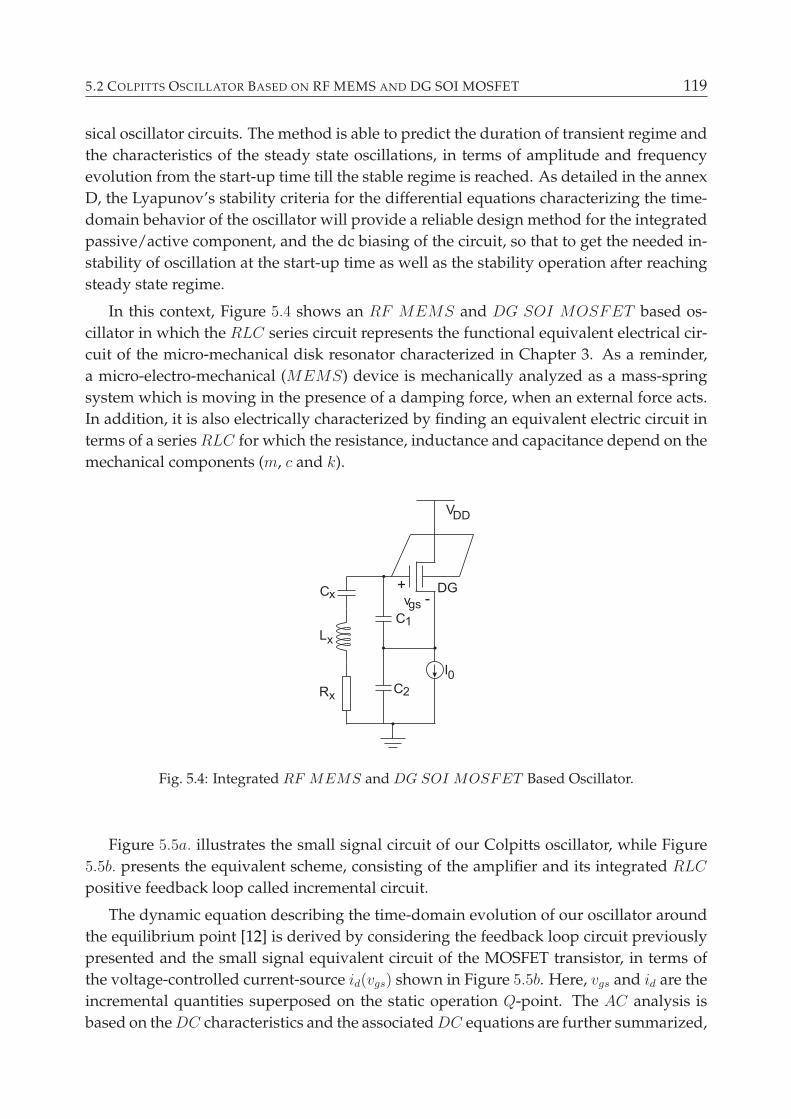
5.2 COLPITTS OSCILLATOR BASED ON RF MEMS AND DG SOI MOSFET 119
sical oscillator circuits. The method is able to predict the duration of transient regime and
the characteristics of the steady state oscillations, in terms of amplitude and frequency
evolution from the start-up time till the stable regime is reached. As detailed in the annex
D, the Lyapunov’s stability criteria for the differential equations characterizing the time-
domain behavior of the oscillator will provide a reliable design method for the integrated
passive/active component, and the dc biasing of the circuit, so that to get the needed in-
stability of oscillation at the start-up time as well as the stability operation after reaching
steady state regime.
In this context, Figure 5.4 shows an RF MEMS and DG SOI MOSFET based os-
cillator in which the RLC series circuit represents the functional equivalent electrical cir-
cuit of the micro-mechanical disk resonator characterized in Chapter 3. As a reminder,
a micro-electro-mechanical (MEMS) device is mechanically analyzed as a mass-spring
system which is moving in the presence of a damping force, when an external force acts.
In addition, it is also electrically characterized by finding an equivalent electric circuit in
terms of a seriesRLC for which the resistance, inductance and capacitance depend on the
mechanical components (m, c and k).
Fig. 5.4: Integrated RF MEMS and DG SOI MOSFET Based Oscillator.
Figure 5.5a. illustrates the small signal circuit of our Colpitts oscillator, while Figure
5.5b. presents the equivalent scheme, consisting of the amplifier and its integrated RLC
positive feedback loop called incremental circuit.
The dynamic equation describing the time-domain evolution of our oscillator around
the equilibrium point [12] is derived by considering the feedback loop circuit previously
presented and the small signal equivalent circuit of the MOSFET transistor, in terms of
the voltage-controlled current-source id(vgs) shown in Figure 5.5b. Here, vgs and id are the
incremental quantities superposed on the static operation Q-point. The AC analysis is
based on theDC characteristics and the associatedDC equations are further summarized,
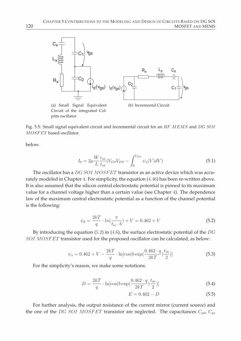
120CHAPTER 5 CONTRIBUTIONS TO THE MODELING AND DESIGN OF CIRCUITS BASED ON DG SOI
MOSFET AND MEMS
(a) Small Signal Equivalent
Circuit of the integrated Col-
pitts oscillator
(b) Incremental Circuit
Fig. 5.5: Small signal equivalent circuit and incremental circuit for an RF MEMS and DG SOI
MOSFET based oscillator.
below.
I0 = 2µW
L
ǫox
tox
(VGSVDS −∫ VDS
0
ψs(V )dV ) (5.1)
The oscillator has a DG SOI MOSFET transistor as an active device which was accu-
rately modeled in Chapter 4. For simplicity, the equation (4.46) has been re-written above.
It is also assumed that the silicon central electrostatic potential is pinned to its maximum
value for a channel voltage higher than a certain value (see Chapter 4). The dependence
law of the maximum central electrostatic potential as a function of the channel potential
is the following:
ψ0 =2kT
q· ln(
π
tsi · b) + V = 0.462 + V (5.2)
By introducing the equation (5.2) in (4.6), the surface electrostatic potential of the DG
SOI MOSFET transistor used for the proposed oscillator can be calculated, as below:
ψs = 0.462 + V − 2kT
q· ln[cos(b exp(
0.462 · q2kT
)tSi
2)] (5.3)
For the simplicity’s reason, we make some notations:
D =2kT
q· ln[cos(b exp(
0.462 · q2kT
)tSi
2)] (5.4)
E = 0.462 −D (5.5)
For further analysis, the output resistance of the current mirror (current source) and
the one of the DG SOI MOSFET transistor are neglected. The capacitances Cgd, Cgs
5.2 COLPITTS OSCILLATOR BASED ON RF MEMS AND DG SOI MOSFET 121
and Cds are neglected for the equivalent incremental circuit, due to the small associated
reactances at the RF frequencies. The active device is assumed to always operate in the
pinch-off region (VDS ≥ VGS − Vth where Vth represents the threshold voltage).
In the design of oscillator circuits, it is necessary to find relationships between the
circuit parameters and the oscillator characteristics in order to satisfy the design require-
ments. It is the purpose of the further analysis to establish the relation between the spec-
ifications and the design constraints.
From the small signal circuit of the oscillator (Figure 5.5b.), the ac currents flowing
through the circuit and the voltages dropped on the elements can be calculated as follows:
iC1 = C1dvgs
dt(5.6)
vCx =C1
Cx
· vgs (5.7)
vRx = C1Rx
dvgs
dt(5.8)
vLx = C1Lx
d2vgs
dt2(5.9)
By applying Kirchhoff’s laws on the circuit, the following equations are obtained:
vC2 = C1Lx
d2vgs
dt2+ C1Rx
dvgs
dt+ (
C1
Cx
+ 1)vgs (5.10)
id(vgs) + iC2 + iCx = 0 (5.11)
By introducing the equations (5.6) - (5.10) in the equation (5.11), a third order differ-
ential equation is derived. Even if apparently we have four components able to store
energy (Cx, C1, C2 and L2), one can easily see that Cx and C2 can be replaced by a single
equivalent capacitance, and thus, finally, we get a circuit with three elements able to store
energy (and thus a third order system is justified for our oscillator). The equation (5.11)
governs the functionality of the oscillator in the time domain and can be interpreted as
a time-domain ”transfer function” of the oscillator because of the output voltage related
with the input voltage (see Figure 5.4).
d3vgs
dt3+Rx
Lx
· d2vgs
dt2+
1
LxC· dvgs
dt= − 1
LxC1C2
· id(vgs) (5.12)
The notations used in the previous equation are as follows:
122CHAPTER 5 CONTRIBUTIONS TO THE MODELING AND DESIGN OF CIRCUITS BASED ON DG SOI
MOSFET AND MEMS
id(vgs) = gmvgs + i (5.13)
i = 2µW
L
ǫox
tox
(v2
gs
2− E · vgs + Vth(E − Vth
2)) (5.14)
gm = 2µW
L
ǫox
tox
(vgs − Vth) (5.15)
1
C=
1
Cx
+1
C1
+1
C2
(5.16)
F = 2µW
L
ǫox
tox
(5.17)
Note that the above small-signal analysis is performed with respect to the real time t
variable.
One can see that the non-linear circuit behavior is characterized by the third-order
differential equation (5.12), which, if numerically solved, this can provide the transient
and the steady state oscillation signal, for a proper designed circuit. The methodology
used here will help us to design the active and/or passive components of the oscillator
components so that to get the desired oscillation functionality. In addition, based on the
perturbation theory (presented in detail in the Appendix D), one can demonstrate that the
above equation (5.12) describes an oscillator with shifting bias, which means that the final
steady state oscillation will end up with a dc signal component superposed to the initial
dc biasing of the oscillator, as treated in Buonomo [12], which can trigger the oscillator in
the class-C operation. Thus, one can predict the operation region of the amplifier, based
on this perturbation modeling. This iterative perturbation method is used in order to
analyze the transient evolution and steady-state oscillations for our proposed oscillator
based on RF MEMS and DG SOI MOSFET devices. In accordance with it, a small
dimensionless perturbation parameter ǫ is introduced and assumed to be related to the
circuit losses. Thus, this perturbation parameter is defined as the inverse of the circuit
quality factor Q as follows:
ǫ =Rx
ω0Lx
(5.18)
and ω0 =√
1LxC
. Here, it is important to emphasize, that the omega zero represents the
natural resonance of theRLC circuit, which coincides with the oscillation frequency of the
ideal oscillator, where no losses are present in the circuit. In the presence of the losses, the
perturbation theory can predict a solution asymptotically closed to the experimental re-
sult, in terms of both amplitude and frequency of oscillation, which are both shifted from
their corresponding values for the ideal oscillator. The higher the order of approximation
used for deducing the oscillation solution, the more accurate fit between the theoretical
and experimental value of the oscillation frequency and the oscillation amplitude of real
oscillator is obtained. By further processing the equation (5.12), a normalized equation is
5.2 COLPITTS OSCILLATOR BASED ON RF MEMS AND DG SOI MOSFET 123
derived, in terms of dimensionless time, t′ and input voltage, vgs/Vth. Thus, a dimension-
less time t′ = ωot and a dimensionless variable x = vgsVth
are used in the equation (5.12) and
the following normalized perturbation equation is derived:
(d3
dt′3+ ǫ · d
2
dt′2+
d
dt′)x = ǫ
F (Vth + E)
RxC1C2ω20
· (x+ αVthx2 +
β
Vth
) (5.19)
where α = − 32(Vth+E)
and β = −Vth · 2E−Vth2(vth+E)
.
On the other hand, as written in the Annex D, the general equation describing the
third order oscillator with shifting bias has the following form: ( d3
dt3+ ǫa d2
dt2+ b d
dt+ ǫc)x =
ǫ(k2d2
dt2+ ǫk1
ddt
+ k0)f(x). By making the identification between the above-mentioned two
equations, the constants a, b, c, k0, k1 and k2 and the non-linear function f(x) (which
describes the behavior of the active device around the equilibrium point) are obtained as
follows:
a = b = 1 (5.20)
c = k1 = k2 = 0 (5.21)
k0 =F (Vth + E)
RxC1C2ω20
(5.22)
f(x) = x+ αVthx2 +
β
Vth
(5.23)
If the oscillator is correctly designed, at the level of both feed-back loop and amplifier,
then the numerical solution of the equation (5.19) will provide the oscillation waveform
x(t), in terms of oscillation frequency and amplitude for both the transient and the steady
state regime. Within the thesis we shall learn how to design the circuit parameter for ob-
taining a stable oscillation and we shall determine the oscillation characteristics by means
of the perturbation method, where both x and f(x) values, which are specific to active
device, will be expressed as complex functions (i.e., functions written in the imaginary
domain) of perturbation parameter and the multitude of signal harmonics. The advan-
tage of the perturbation method is the fact that the theoretical solution can be designed
to fit asymptotically the experimental oscillation result by adding an increased number
of perturbation terms, by going to higher approximation orders, as shown below. There-
fore, the key aspect of the perturbation method applied for the analysis and design of
the electronic oscillators is that the solution x(t), the transfer function of active device,
f(x) and the oscillation frequency can be forced to be expressed as complex polynomial
expressions (see the Annex D) depending on the perturbation parameter as below:
x(t) = x0 + ǫx1 + ǫ2x2 + ... (5.24)
ω = ω0(τ) + ǫω1 + ǫ2ω2 + ... (5.25)
x0 = B0(τ(t)) + A0(τ(t))cost (5.26)
124CHAPTER 5 CONTRIBUTIONS TO THE MODELING AND DESIGN OF CIRCUITS BASED ON DG SOI
MOSFET AND MEMS
In the above equations, τ is representing what it is called ”slow time scale”, which
reflects the fact that the time variation of the dc component of the emerging oscillation, as
well as its amplitude envelope are slower with respect to the rapid variation with the time
of the oscillation, itself , x(t). Mathematically the relation between the two time scales is
expressed by : τ = ǫ ∗ t.The detailed description of the oscillation solution is presented in the Annex D.
Here, it is worth to emphasize that B0 is the dc component of the emerging oscillation
and A0 is the amplitude of oscillation, both of them being slowly variable with time in
the transient regime, if we compare their time variation with respect to the period of
oscillation. For a more detailed description of the perturbation method, one can study
the Annex D of the thesis, where characterization of the circuit up to the second order
approximation is developed.
The first order approximation methodology is enough for designing the oscillator.
Anyway, the second order approximation was also used here, but only for an accurate
description of the frequency deviation from the ideal value of the oscillation signal.
5.2.1 Analysis and design of integration of a Colpitts oscillator by means
of perturbation method based on first order approximation
According to this approximation, only the terms in epsilon at the first power and free
terms will be kept from the calculation. Following the entire procedure described in the
Annex D, for the first order approximation methodology and considering that only the
fundamental harmonic is present in the circuit, we get the following general final form of
our normalized perturbation equations:
ejν(−3ω2dA0
dτ− 3ω
dω
dτA0 − jω3A1 − aω2A0 + b0
dA0
dτ+ jωb0A1 + jωb1A0 + cA0)
+b0dB0
dτ+ cB0 = ejν(k0 − k2ω
2)F1,0 + k0F0,0 (5.27)
Balancing the real and imaginary part of the amplitude of fundamental harmonic (A0)
and the DC component (B0) of the general first order equation, we get the following
system of equations:
dB0
dτ= k0F0,0 − cB0 (5.28)
dA0
dτ=
1
2[(k2 − k0)F1,0 + (c− a)A0] (5.29)
where, as shown in the Annex D, the expressions for the above amounts F0,0 and F1,0
specific to first order approximation approach for our oscillator are given below:
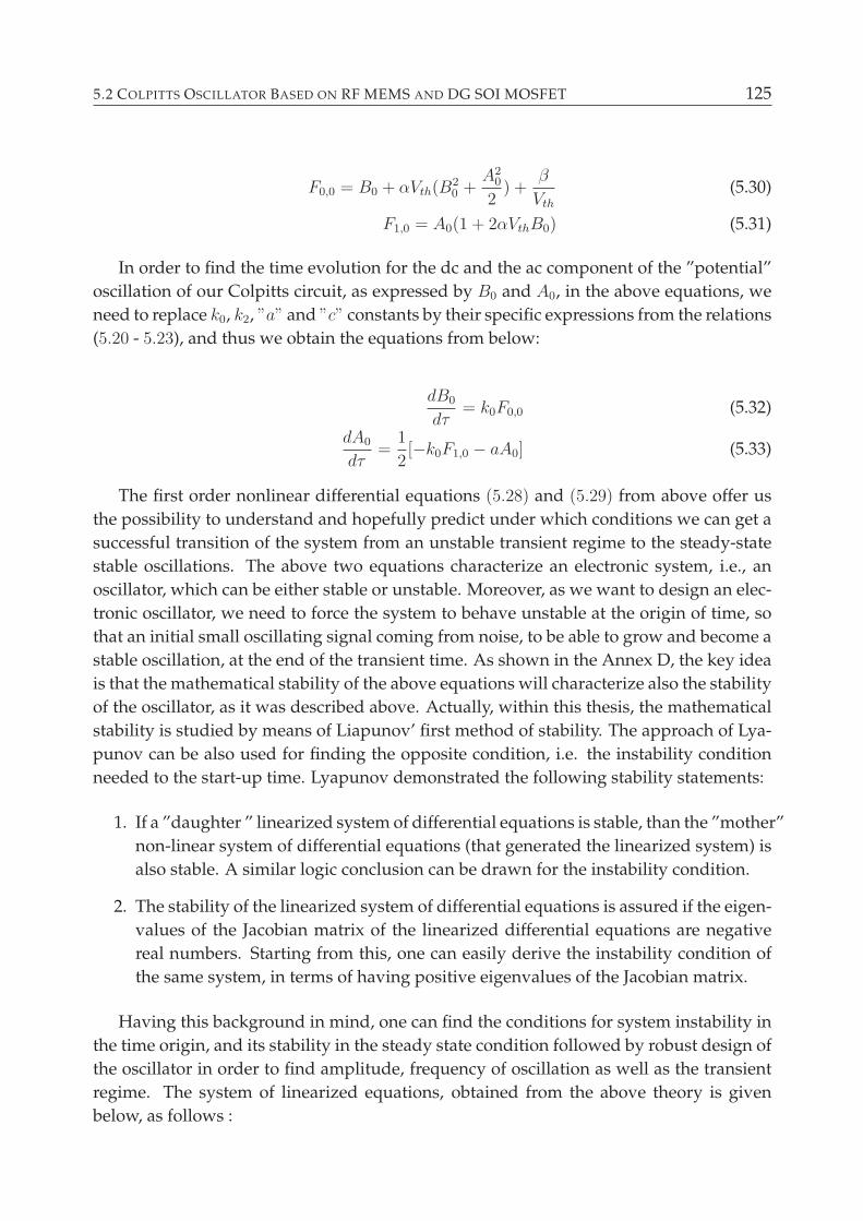
5.2 COLPITTS OSCILLATOR BASED ON RF MEMS AND DG SOI MOSFET 125
F0,0 = B0 + αVth(B20 +
A20
2) +
β
Vth
(5.30)
F1,0 = A0(1 + 2αVthB0) (5.31)
In order to find the time evolution for the dc and the ac component of the ”potential”
oscillation of our Colpitts circuit, as expressed by B0 and A0, in the above equations, we
need to replace k0, k2, ”a” and ”c” constants by their specific expressions from the relations
(5.20 - 5.23), and thus we obtain the equations from below:
dB0
dτ= k0F0,0 (5.32)
dA0
dτ=
1
2[−k0F1,0 − aA0] (5.33)
The first order nonlinear differential equations (5.28) and (5.29) from above offer us
the possibility to understand and hopefully predict under which conditions we can get a
successful transition of the system from an unstable transient regime to the steady-state
stable oscillations. The above two equations characterize an electronic system, i.e., an
oscillator, which can be either stable or unstable. Moreover, as we want to design an elec-
tronic oscillator, we need to force the system to behave unstable at the origin of time, so
that an initial small oscillating signal coming from noise, to be able to grow and become a
stable oscillation, at the end of the transient time. As shown in the Annex D, the key idea
is that the mathematical stability of the above equations will characterize also the stability
of the oscillator, as it was described above. Actually, within this thesis, the mathematical
stability is studied by means of Liapunov’ first method of stability. The approach of Lya-
punov can be also used for finding the opposite condition, i.e. the instability condition
needed to the start-up time. Lyapunov demonstrated the following stability statements:
1. If a ”daughter ” linearized system of differential equations is stable, than the ”mother”
non-linear system of differential equations (that generated the linearized system) is
also stable. A similar logic conclusion can be drawn for the instability condition.
2. The stability of the linearized system of differential equations is assured if the eigen-
values of the Jacobian matrix of the linearized differential equations are negative
real numbers. Starting from this, one can easily derive the instability condition of
the same system, in terms of having positive eigenvalues of the Jacobian matrix.
Having this background in mind, one can find the conditions for system instability in
the time origin, and its stability in the steady state condition followed by robust design of
the oscillator in order to find amplitude, frequency of oscillation as well as the transient
regime. The system of linearized equations, obtained from the above theory is given
below, as follows :
126CHAPTER 5 CONTRIBUTIONS TO THE MODELING AND DESIGN OF CIRCUITS BASED ON DG SOI
MOSFET AND MEMS
dB0
dτ= k0
∂F0,0
∂B0
B0 + k0∂F0,0
∂A0
A0 (5.34)
dA0
dτ= −k0
1
2
∂F1,0
∂B0
B0 +1
2[−k0
∂F1,0
∂A0
− a]A0 (5.35)
With all these equations from above we can now derive the stability and instability
needed for a robust design of our Colpitts oscillator.
The stability conditions, as per Lyapunov method applied to our oscillator are given
below:
k0∂F0,0
∂B0
− k0
2
∂F1,0
∂A0
− a
2< 0 (5.36)
k0∂F0,0
∂B0
(−k0
2
∂F1,0
∂A0
− a
2) > −k0
k0
2
∂F0,0
∂A0
· ∂F1,0
∂B0
(5.37)
After doing further calculations and arrangements the conditions of stability become:
a > k0F1,0
A0
(5.38)
a > k0(F1,0
A0
− 2α2V 2thA
20
A0
F1,0
) (5.39)
Similarly, following the Lyapunov theory and doing all calculations, the instability
condition for our oscillator, specific to time origin operation will bring the following re-
sult:
W
L>tox
ǫox
· 1
2µ· RxC1C2ω
20
vth + E(5.40)
If the mentioned stability and instability conditions are fulfilled, then by solving the
nonlinear system of differential equations, in the time domain, one can get the amplitude
envelope evolution in the transient (start-up) and the steady state regime of the first order
approximated solution.
Thus, the system of first-order equations (D.46) and (D.47), formed on the particular
coefficients obtained for our proposed RF MEMS and DG SOI MOSFET based oscil-
lator, will show the transition of the circuit to the steady-state oscillation and provides
a way to calculate the steady-state values for A0 and B0. In order to get the stationary
values, their derivatives, as provided from the equations (5.27 - 5.28) are assumed to be
zero and the steady state expressions for B0 and A0 result in:
5.2 COLPITTS OSCILLATOR BASED ON RF MEMS AND DG SOI MOSFET 127
B0 = − 1 + k0
2αk0Vth
(5.41)
A0 =
√
k20(1−4αβ)−1
2
αk0Vth
(5.42)
One can see that they strongly depend on the elements of the RF MEMS resonator
from the positive loop (Rx, Lx and Cx) and on the DG SOI MOSFET device used in the
oscillator.
With regard to the transient evolution of the oscillator, our interest is in the determina-
tion of the envelope for the oscillation amplitude until the steady-state regime is reached,
as follows. First of all, as the oscillation solution provided by the first order analysis has
the form: x(τ) = B0(τ)+A0(τ)cos(τ), then it is easy to understand that not only during the
transient, but also at the steady state, the amplitude envelopes (maximum and minimum
values of x(τ)) of the oscillation are obtained by performing the sum and subtraction of
A0 and B0. Their dependencies on time are calculated by solving the system of first-order
nonlinear equations (5.27) and (5.28) as follows:
d2A0
dτ 2= −dA0
dτ+ (
k20 − 1
4− αβk2
0) · A0 −α2V 2
thk20
2A3
0 (5.43)
B0 = − 1
αk0Vth
· (k0 + 1
2+
1
A0
dA0
dτ) (5.44)
The above system of non-linear equations was solved numerically, based on the known
circuit values for both amplifier and feed-back loop components, in our case the DG SOI
MOSFET transistor and RLC circuit associated to the integrated RF MEMS resonator.
So in order to have a practical application of the above-described RF MEMS and DG
SOI MOSFET based oscillator, we take into account the micro-mechanical disk res-
onator described in detail in Subsection 3.4.4.4 from Chapter 3, for which the values of the
behavioralRLC series circuit obtained experimentally ( [119]) are: Rx = 745 Ω, Lx = 0.523
mH and Cx = 36.6 aF . We also assume that: C1 = C2 = 0.6 pF , Vth = 0.4 V , I0 = 1.7
mA and W/L = 1500. The constant quantities used to describe the DG SOI MOSFET
transistor are those from Chapter 4, where the entire dc and ac analyses were done. We
also neglect the term of β
vthin the equation (5.21) because it is very small related to the
other terms of the function f(x).
In Figure 5.6 we show the asymmetric amplitude envelopes of vgs which are obtained
by following the procedure presented above. The preliminary numerical results show
that the steady-state oscillation is reached in a very short time of 1.5 ns which, if con-
firmed by further modeling could prove the superior performance of an Colpitts oscilla-
tor formed on MEMS resonator and DG SOI MOSFET device over the bulk Colpitts
oscillators.
128CHAPTER 5 CONTRIBUTIONS TO THE MODELING AND DESIGN OF CIRCUITS BASED ON DG SOI
MOSFET AND MEMS
0,0 0,4 0,8 1,2 1,6 2,0 2,4 2,8 3,2 3,6-0,2
0,0
0,2
0,4
0,6
0,8
1,0
Env
elop
es (V
)
Time (ns)
(-A0 + B0) Vth
(A0 + B0) Vth
Fig. 5.6: Amplitude Envelope of the fundamental harmonic as a function of time for the case of
first order approximation of the integrated Colpitts oscillator based on RF MEMS resonator..
5.2.2 Analysis and design of integration of a Colpitts oscillator by means
of perturbation method based on second order approximation
The design of the integrated oscillator based on the perturbation method, where the sec-
ond order approximation is used can provide a further improved accuracy of the fit be-
tween the theoretical solution and the experimental one, but the improvement is not es-
sential, at least when the amplitude envelope of fundamental harmonic is concerned.
Much higher motivation for the use of the second order approximation in the design of
oscillator comes from the need of theoretical evaluation of the oscillation frequency de-
viation from the natural resonance frequency of the fee-back loop circuit. As shown in
the previous sub-section, within this second order approximation, the time evolution of
the oscillation frequency with the slow time scale is: ω = ω0 + ǫω1 + ǫ2ω2. Actually, the
frequency will have a small deviation from the natural frequency of the oscillator because
of the losses and the nonlinear effects which are treated with the perturbation method.
For this purpose, the second order approximation has been developed by keeping only
the terms assigned to the ǫ2 in all the terms of the general equation of the third order
differential equation, and the term ω2 is obtained as presented below - see Appendix D.
ω2 =1
2A0
[(k2 − k0)Im(R1,1) − k1F1,0 + b2A0 − 2k2dF1,0
dτ+ 3
d2A0
dτ 2] (5.45)
By taking into account the particular values for the proposed oscillator based on DG
SOI MOSFET transistor and RF MEMS resonator, the frequency deviation ω2 be-
comes:
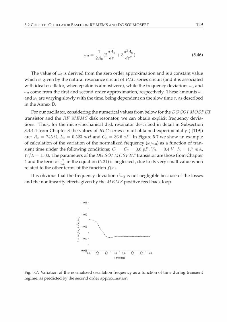
5.2 COLPITTS OSCILLATOR BASED ON RF MEMS AND DG SOI MOSFET 129
ω2 =1
2A0
(2dA0
dτ+ 3
d2A0
dτ 2) (5.46)
The value of ω0 is derived from the zero order approximation and is a constant value
which is given by the natural resonance circuit of RLC series circuit (and it is associated
with ideal oscillator, when epsilon is almost zero), while the frequency deviations ω1 and
ω2 come from the first and second order approximation, respectively. These amounts ω1
and ω2 are varying slowly with the time, being dependent on the slow time τ , as described
in the Annex D.
For our oscillator, considering the numerical values from below for theDGSOI MOSFET
transistor and the RF MEMS disk resonator, we can obtain explicit frequency devia-
tions. Thus, for the micro-mechanical disk resonator described in detail in Subsection
3.4.4.4 from Chapter 3 the values of RLC series circuit obtained experimentally ( [119])
are: Rx = 745 Ω, Lx = 0.523 mH and Cx = 36.6 aF . In Figure 5.7 we show an example
of calculation of the variation of the normalized frequency (ω/ω0) as a function of tran-
sient time under the following conditions: C1 = C2 = 0.6 pF , Vth = 0.4 V , I0 = 1.7 mA,
W/L = 1500. The parameters of theDG SOI MOSFET transistor are those from Chapter
4 and the term of β
vthin the equation (5.21) is neglected , due to its very small value when
related to the other terms of the function f(x).
It is obvious that the frequency deviation ǫ2ω2 is not negligible because of the losses
and the nonlinearity effects given by the MEMS positive feed-back loop.
0,0 0,5 1,0 1,5 2,0 2,5 3,0 3,50,995
1,000
1,005
1,010
1,015
Time (ns)
Fig. 5.7: Variation of the normalized oscillation frequency as a function of time during transient
regime, as predicted by the second order approximation.
130CHAPTER 5 CONTRIBUTIONS TO THE MODELING AND DESIGN OF CIRCUITS BASED ON DG SOI
MOSFET AND MEMS
5.3 Summary
The purpose of this chapter has been to model and design several circuits applications
based on double-gate SOI MOSFET device and MEMS resonator. Thus, at the begin-
ning of the chapter we showed the operation of a common source amplifier based on
DG SOI MOSFET transistor, where a code written in Verilog A tool was developed for
building a library that contains the proposed compact model of a symmetric un-doped
DG SOI MOSFET device (see Chapter 4). As a case study, this library was then used to
simulate a common source amplifier based on the previous library forDGSOI MOSFET
transistor. It was shown that the Verilog A library-based static transfer characteristics of
the common source amplifier using theDG SOI MOSFET looks similar to that obtained
for the same circuit, but where the Matlab code was used for solving the static equations
of the circuit.
Then, in the second part of the chapter, the feasibility of the realization of an integrated
oscillator containing the DG SOI MOSFET transistors and RF MEMS resonators per-
formed in the SOI technology platform has been predicted at the modeling analysis by
using the first and the second order approximation of the perturbation theory. This en-
couraging result might support the experimental research towards ultra small consumer
electronics wireless applications. The chapter has shown, for the first time, how the per-
turbation method can be applied to design a non-linear oscillator comprising of a DG
SOI MOSFET device and a RF MEMS resonator used for the positive feedback loop.
The developed procedure showed the operation and design of the oscillator in time do-
main determining what are the conditions for start-up and for the stability in the steady
state oscillations, as per Lyapunov’ stability theory. The evolution with the time of the
amplitude envelope of the fundamental harmonic and of the oscillation frequency devia-
tion was theoretically predicted for the first time for an integrated Colpitts oscillator built
with DG SOI MOSFET and RF MEMS disk resonator.
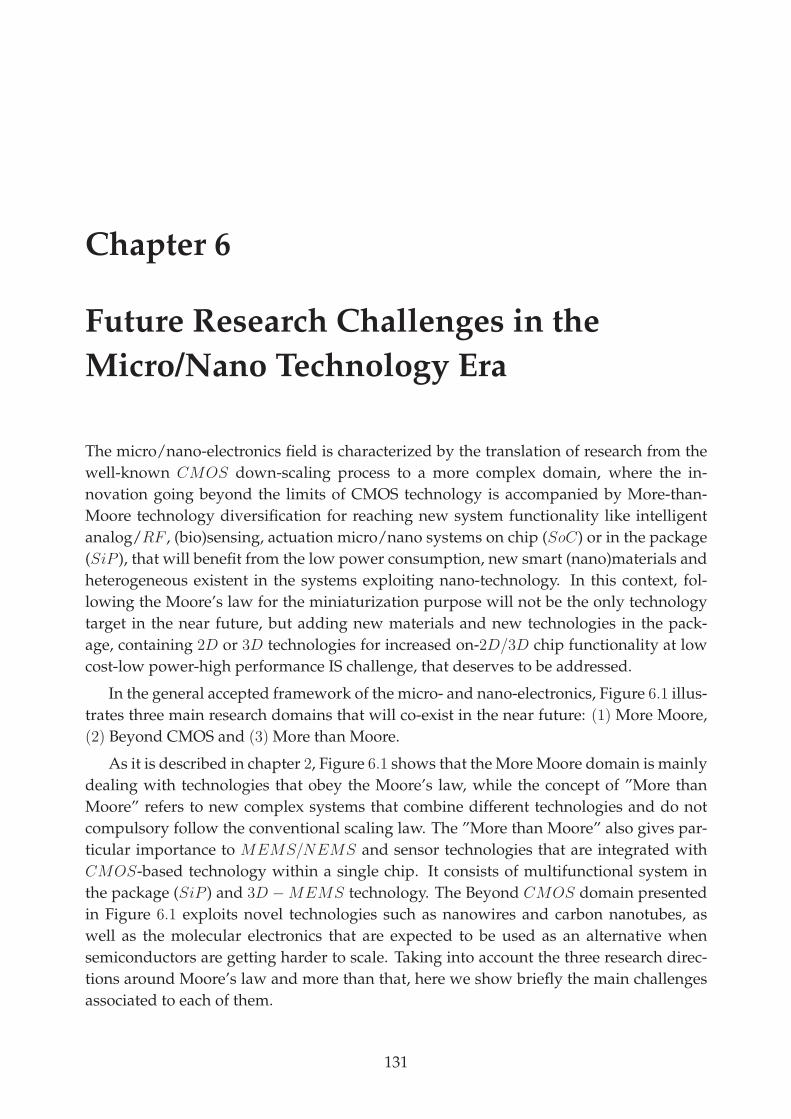
Chapter 6
Future Research Challenges in the
Micro/Nano Technology Era
The micro/nano-electronics field is characterized by the translation of research from the
well-known CMOS down-scaling process to a more complex domain, where the in-
novation going beyond the limits of CMOS technology is accompanied by More-than-
Moore technology diversification for reaching new system functionality like intelligent
analog/RF , (bio)sensing, actuation micro/nano systems on chip (SoC) or in the package
(SiP ), that will benefit from the low power consumption, new smart (nano)materials and
heterogeneous existent in the systems exploiting nano-technology. In this context, fol-
lowing the Moore’s law for the miniaturization purpose will not be the only technology
target in the near future, but adding new materials and new technologies in the pack-
age, containing 2D or 3D technologies for increased on-2D/3D chip functionality at low
cost-low power-high performance IS challenge, that deserves to be addressed.
In the general accepted framework of the micro- and nano-electronics, Figure 6.1 illus-
trates three main research domains that will co-exist in the near future: (1) More Moore,
(2) Beyond CMOS and (3) More than Moore.
As it is described in chapter 2, Figure 6.1 shows that the More Moore domain is mainly
dealing with technologies that obey the Moore’s law, while the concept of ”More than
Moore” refers to new complex systems that combine different technologies and do not
compulsory follow the conventional scaling law. The ”More than Moore” also gives par-
ticular importance to MEMS/NEMS and sensor technologies that are integrated with
CMOS-based technology within a single chip. It consists of multifunctional system in
the package (SiP ) and 3D −MEMS technology. The Beyond CMOS domain presented
in Figure 6.1 exploits novel technologies such as nanowires and carbon nanotubes, as
well as the molecular electronics that are expected to be used as an alternative when
semiconductors are getting harder to scale. Taking into account the three research direc-
tions around Moore’s law and more than that, here we show briefly the main challenges
associated to each of them.
131
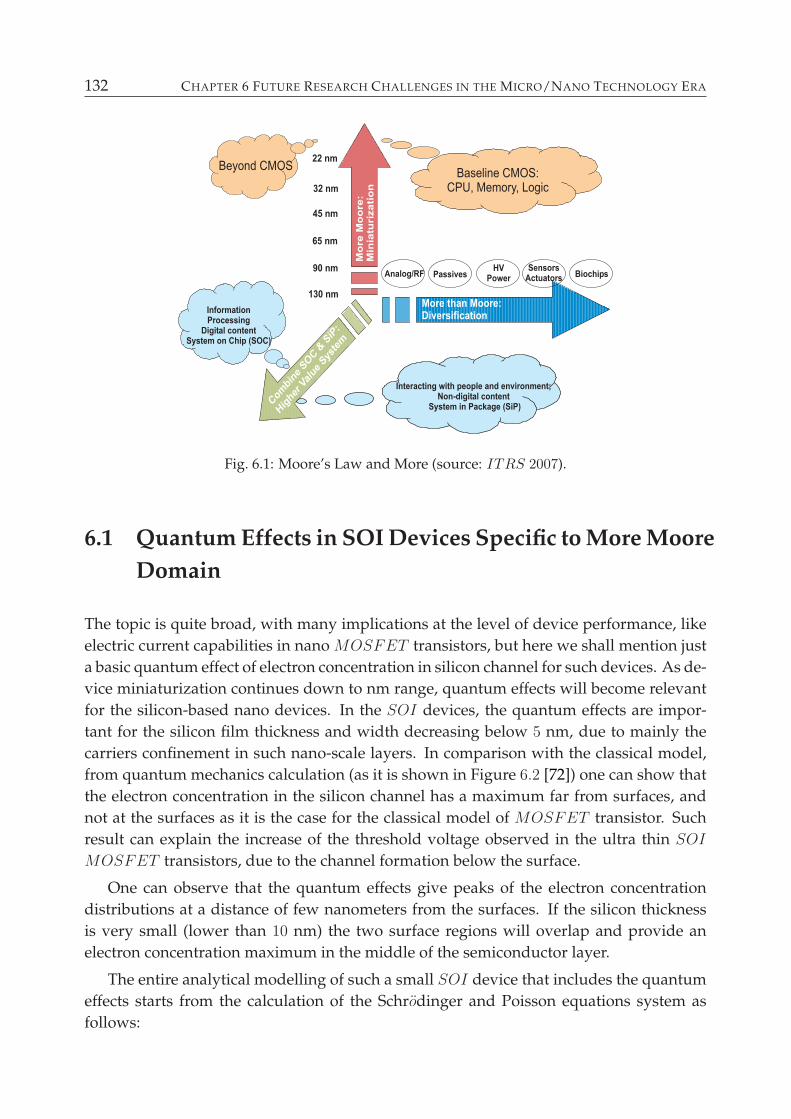
132 CHAPTER 6 FUTURE RESEARCH CHALLENGES IN THE MICRO/NANO TECHNOLOGY ERA
Fig. 6.1: Moore’s Law and More (source: ITRS 2007).
6.1 Quantum Effects in SOI Devices Specific to More Moore
Domain
The topic is quite broad, with many implications at the level of device performance, like
electric current capabilities in nano MOSFET transistors, but here we shall mention just
a basic quantum effect of electron concentration in silicon channel for such devices. As de-
vice miniaturization continues down to nm range, quantum effects will become relevant
for the silicon-based nano devices. In the SOI devices, the quantum effects are impor-
tant for the silicon film thickness and width decreasing below 5 nm, due to mainly the
carriers confinement in such nano-scale layers. In comparison with the classical model,
from quantum mechanics calculation (as it is shown in Figure 6.2 [72]) one can show that
the electron concentration in the silicon channel has a maximum far from surfaces, and
not at the surfaces as it is the case for the classical model of MOSFET transistor. Such
result can explain the increase of the threshold voltage observed in the ultra thin SOI
MOSFET transistors, due to the channel formation below the surface.
One can observe that the quantum effects give peaks of the electron concentration
distributions at a distance of few nanometers from the surfaces. If the silicon thickness
is very small (lower than 10 nm) the two surface regions will overlap and provide an
electron concentration maximum in the middle of the semiconductor layer.
The entire analytical modelling of such a small SOI device that includes the quantum
effects starts from the calculation of the Schrodinger and Poisson equations system as
follows:
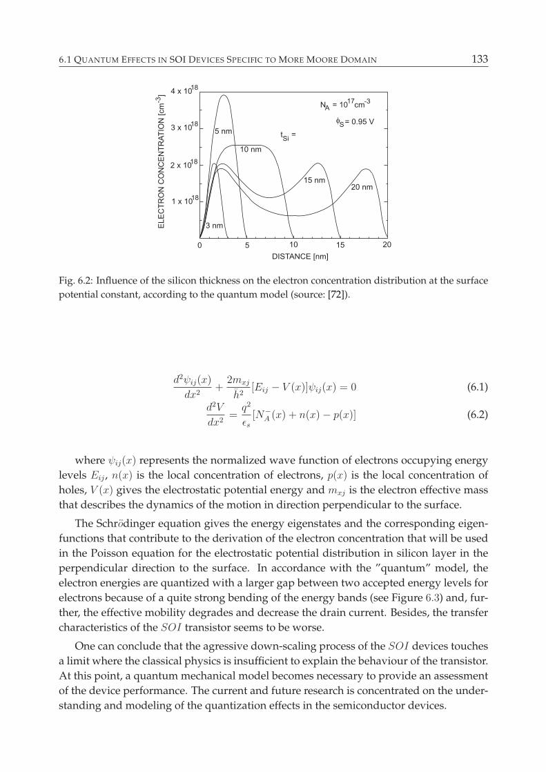
6.1 QUANTUM EFFECTS IN SOI DEVICES SPECIFIC TO MORE MOORE DOMAIN 133
Fig. 6.2: Influence of the silicon thickness on the electron concentration distribution at the surface
potential constant, according to the quantum model (source: [72]).
d2ψij(x)
dx2+
2mxj
h2[Eij − V (x)]ψij(x) = 0 (6.1)
d2V
dx2=q2
ǫs[N−
A (x) + n(x) − p(x)] (6.2)
where ψij(x) represents the normalized wave function of electrons occupying energy
levels Eij , n(x) is the local concentration of electrons, p(x) is the local concentration of
holes, V (x) gives the electrostatic potential energy and mxj is the electron effective mass
that describes the dynamics of the motion in direction perpendicular to the surface.
The Schrodinger equation gives the energy eigenstates and the corresponding eigen-
functions that contribute to the derivation of the electron concentration that will be used
in the Poisson equation for the electrostatic potential distribution in silicon layer in the
perpendicular direction to the surface. In accordance with the ”quantum” model, the
electron energies are quantized with a larger gap between two accepted energy levels for
electrons because of a quite strong bending of the energy bands (see Figure 6.3) and, fur-
ther, the effective mobility degrades and decrease the drain current. Besides, the transfer
characteristics of the SOI transistor seems to be worse.
One can conclude that the agressive down-scaling process of the SOI devices touches
a limit where the classical physics is insufficient to explain the behaviour of the transistor.
At this point, a quantum mechanical model becomes necessary to provide an assessment
of the device performance. The current and future research is concentrated on the under-
standing and modeling of the quantization effects in the semiconductor devices.
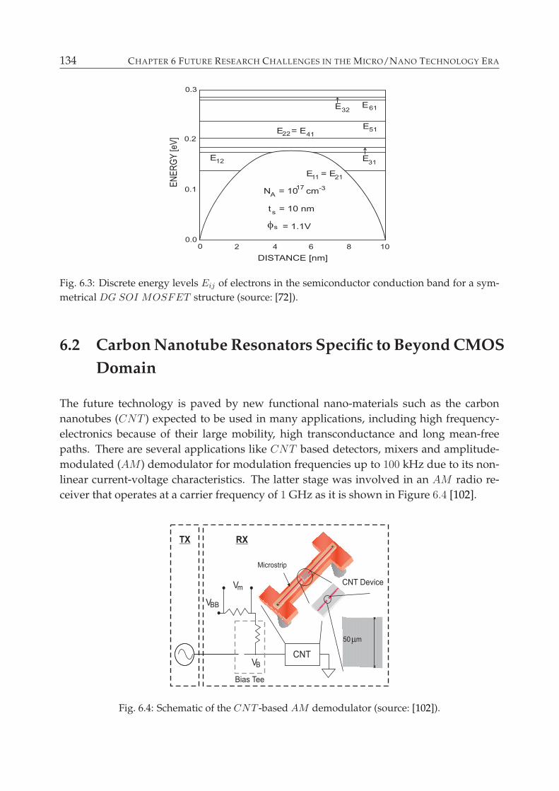
134 CHAPTER 6 FUTURE RESEARCH CHALLENGES IN THE MICRO/NANO TECHNOLOGY ERA
Fig. 6.3: Discrete energy levels Eij of electrons in the semiconductor conduction band for a sym-
metrical DG SOI MOSFET structure (source: [72]).
6.2 Carbon Nanotube Resonators Specific to Beyond CMOS
Domain
The future technology is paved by new functional nano-materials such as the carbon
nanotubes (CNT ) expected to be used in many applications, including high frequency-
electronics because of their large mobility, high transconductance and long mean-free
paths. There are several applications like CNT based detectors, mixers and amplitude-
modulated (AM ) demodulator for modulation frequencies up to 100 kHz due to its non-
linear current-voltage characteristics. The latter stage was involved in an AM radio re-
ceiver that operates at a carrier frequency of 1 GHz as it is shown in Figure 6.4 [102].
Fig. 6.4: Schematic of the CNT -based AM demodulator (source: [102]).
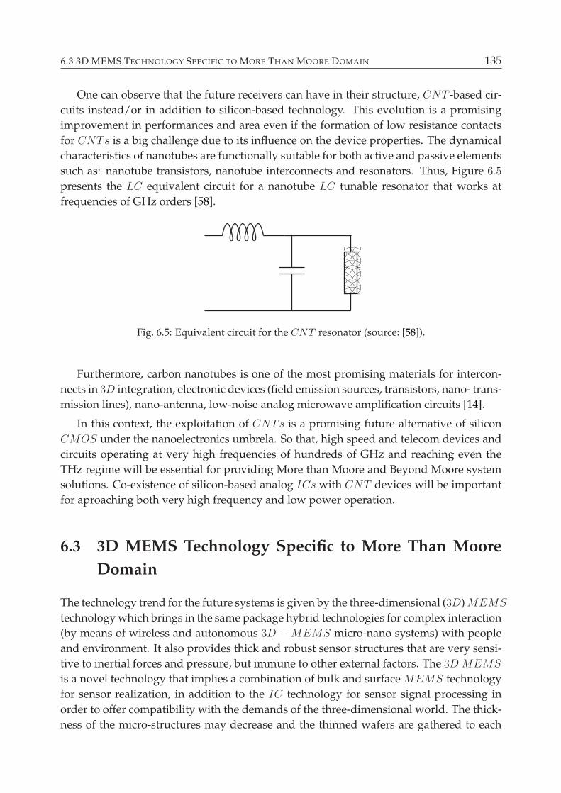
6.3 3D MEMS TECHNOLOGY SPECIFIC TO MORE THAN MOORE DOMAIN 135
One can observe that the future receivers can have in their structure, CNT -based cir-
cuits instead/or in addition to silicon-based technology. This evolution is a promising
improvement in performances and area even if the formation of low resistance contacts
for CNTs is a big challenge due to its influence on the device properties. The dynamical
characteristics of nanotubes are functionally suitable for both active and passive elements
such as: nanotube transistors, nanotube interconnects and resonators. Thus, Figure 6.5
presents the LC equivalent circuit for a nanotube LC tunable resonator that works at
frequencies of GHz orders [58].
aaaa
Fig. 6.5: Equivalent circuit for the CNT resonator (source: [58]).
Furthermore, carbon nanotubes is one of the most promising materials for intercon-
nects in 3D integration, electronic devices (field emission sources, transistors, nano- trans-
mission lines), nano-antenna, low-noise analog microwave amplification circuits [14].
In this context, the exploitation of CNTs is a promising future alternative of silicon
CMOS under the nanoelectronics umbrela. So that, high speed and telecom devices and
circuits operating at very high frequencies of hundreds of GHz and reaching even the
THz regime will be essential for providing More than Moore and Beyond Moore system
solutions. Co-existence of silicon-based analog ICs with CNT devices will be important
for aproaching both very high frequency and low power operation.
6.3 3D MEMS Technology Specific to More Than Moore
Domain
The technology trend for the future systems is given by the three-dimensional (3D)MEMS
technology which brings in the same package hybrid technologies for complex interaction
(by means of wireless and autonomous 3D −MEMS micro-nano systems) with people
and environment. It also provides thick and robust sensor structures that are very sensi-
tive to inertial forces and pressure, but immune to other external factors. The 3D MEMS
is a novel technology that implies a combination of bulk and surface MEMS technology
for sensor realization, in addition to the IC technology for sensor signal processing in
order to offer compatibility with the demands of the three-dimensional world. The thick-
ness of the micro-structures may decrease and the thinned wafers are gathered to each
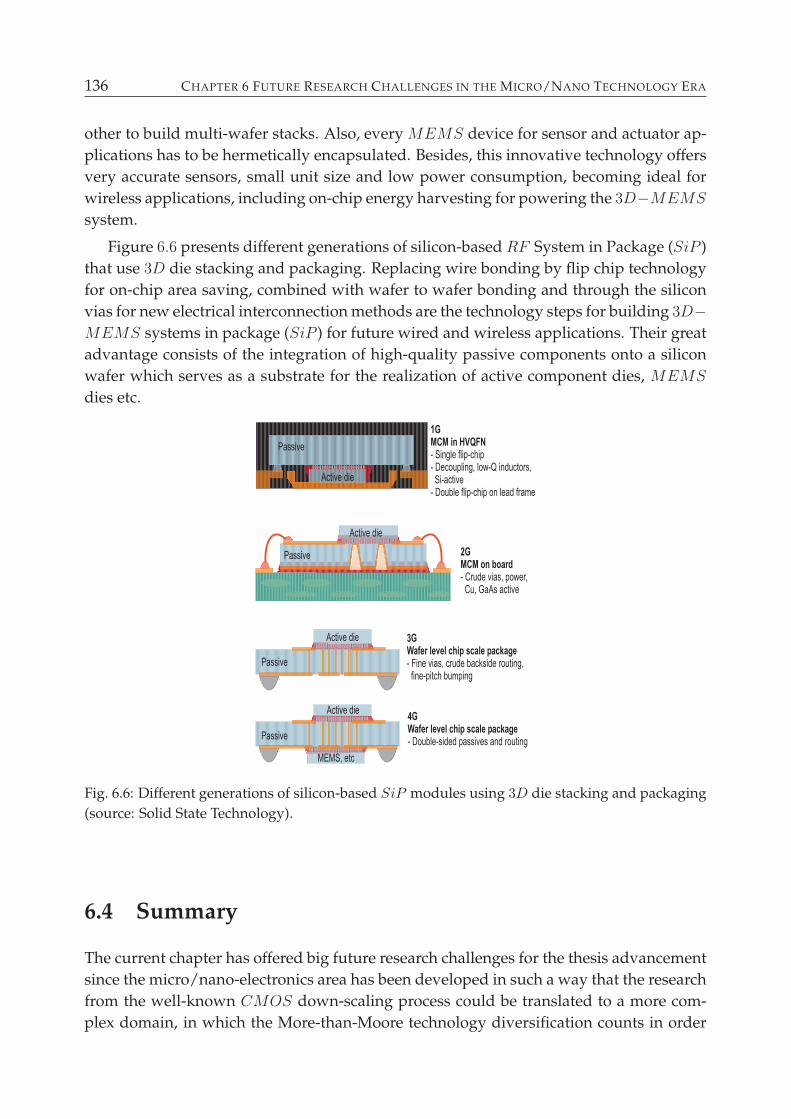
136 CHAPTER 6 FUTURE RESEARCH CHALLENGES IN THE MICRO/NANO TECHNOLOGY ERA
other to build multi-wafer stacks. Also, every MEMS device for sensor and actuator ap-
plications has to be hermetically encapsulated. Besides, this innovative technology offers
very accurate sensors, small unit size and low power consumption, becoming ideal for
wireless applications, including on-chip energy harvesting for powering the 3D−MEMS
system.
Figure 6.6 presents different generations of silicon-based RF System in Package (SiP )
that use 3D die stacking and packaging. Replacing wire bonding by flip chip technology
for on-chip area saving, combined with wafer to wafer bonding and through the silicon
vias for new electrical interconnection methods are the technology steps for building 3D−MEMS systems in package (SiP ) for future wired and wireless applications. Their great
advantage consists of the integration of high-quality passive components onto a silicon
wafer which serves as a substrate for the realization of active component dies, MEMS
dies etc.
Fig. 6.6: Different generations of silicon-based SiP modules using 3D die stacking and packaging
(source: Solid State Technology).
6.4 Summary
The current chapter has offered big future research challenges for the thesis advancement
since the micro/nano-electronics area has been developed in such a way that the research
from the well-known CMOS down-scaling process could be translated to a more com-
plex domain, in which the More-than-Moore technology diversification counts in order
6.4 SUMMARY 137
to reach new system functionality like intelligent analog/RF , (bio)sensing, actuation mi-
cro/nano systems on chip (SoC) or in the package (SiP ). In this context, following the
Moore’s law, the quantum effects in SOI devices (DG SOI MOSFET in this thesis) have
constituted a relevant research topic for the future work since they become significant as
device miniaturization continues to scale down to several nm range. The system formed
on Schrodinger equation and Poisson equation has created the possibility to build a quan-
tum mechanical model which describes the quantization of the electron energy levels
going to a new shape for the electron concentration distribution. The effort should be fo-
cused on the understanding and modeling the quantum effects in the silicon on insulator
devices in order to obtain a pretty accurate analyses.
In addition, the trend given by ”More than Moore” brings the three-dimensionalMEMS
technology which gathers on the same chip hybrid technologies that realize complex in-
teraction with people and environment. Also, the carbon nanotubes are expecting to be
utilized in many applications due to their superior performances over the MEMS de-
vices.

Chapter 7
Conclusions
This dissertation has presented an one-dimensional compact analytical modeling of a
novel symmetric Double-Gate SOI MOSFET transistor, covering the dc and ac anal-
yses. The adopted methodology offers a good characterization of the device in all regions
of operation with the only assumptions of the light doping of the substrate and constant
electron mobility. The model has been implemented in Verilog-A code and then, used
in the circuits simulation. In addition, this work has emphasized the specific challenges
of the analytical modelling for asymmetric DG SOI MOSFET devices, where the com-
plexity of the mathematical equations reaches its limits. Driven by the present scientific
community effort to integrate the RF MEMS vibrating components and the electronic
circuits for getting one chip transceiver in the near future, within thin thesis we have
combined the DG SOI MOSFET circuits with RF MEMS resonators for developing
on-chip frequency generating functions. In this case, a disk MEMS resonators acting as
an RLC series circuit has been located in the positive feed-back loop of an amplifier in
order to get an on-chip oscillator for GHz applications for future transceivers.
7.1 Results of Research Work
The continuous scaling-down process of the channel length over the last four decades
is reaching its limits in terms of gate oxide thickness, short channel effects and power
consumptions. The basic aspects of short channel effects and leakage mechanisms were
described in Chapter 2 for a better understanding of the technology and design solutions
envisaged by the scientific community to overcome them. Now, when we are closed to
the end of ITRS road-map, the dual gate SOI MOSFET devices are expected to re-
place the bulk MOSFET transistors for a better control of the entire device electrostatics.
In parallel, Chapter 3 has offered a general overview on the state-of-the-art in the RF
micro-electro-mechanical systems focusing on new frequency processing functions of the
integrated micro-mechanical circuits. It has been shown that one of the long term targets
of the MEMS domain is the miniaturization of cell phones and other wireless applica-
139
140 CHAPTER 7 CONCLUSIONS
tions, by integrating the expensive off-chip passive components. To make this happen,
on-chip high Q components and functions which can be obtained with vibrating capac-
itive RF MEMS are emerging, even in the GHz range. Within this thesis, it is for the
first time when a model for designing an RF MEMS-based oscillator has been devel-
oped starting from an amplifier with a DG SOI MOSFET transistor and an RF MEMS
resonator located in its positive feed-back loop. Such a design can be the starting point
for the future ultra wide band oscillators serving to the realization of the next generation
of low size/power/noise, fully integrated DG SOI MOSFET transceivers for wireless
applications.
To receive large acceptance, simple and efficient static and dynamic models of the
multi-gate SOI devices should be developed and validated by experimental results. It
has been the purpose of this thesis to show our contribution to the analytical modeling
of un-doped asymmetrical and symmetrical DG SOI MOSFET devices in the static and
dynamic regime.
An original, simple and efficient analytical model has been proposed in this thesis for
the calculation of the electrostatic potential from the central part of the silicon layer in the
symmetric and asymmetric DG SOI MOSFET , starting from the analytical approach
of Poisson’s equation. Then, the distribution of the electrostatic potential in the silicon
film was derived for both cases. Our procedure is based on original mathematical com-
putations implemented in the Matlab code for solving the transcendental equation pro-
viding the minimum electrostatic potential in the middle of the silicon film. Our method
could replace other complex approaches based on Lambert function and smoothing factor
without physical meaning which were previously used for the same electrostatic poten-
tial computation. The mechanical quantum effects and short channel effects appeared in
even this novel device were not studied in our analytical work. Continuing on the same
direction, the electric inversion charge and drain current have been calculated by using
our analytical model in the symmetrical DG SOI MOSFET device, in order to obtain a
complete DC behavior. It is necessary to mention that the silicon thickness of our novel
device is of 20 nm, so that the volume inversion feature was analytically proved.
The thesis has introduced for the first time the idea of the asymmetry behavior of the
symmetric DG SOI MOSFET as a function of the applied channel voltage. The chapter
4 has shown that when the drain voltage is very small, the potentials at the front and back
surfaces are distinct and, thus, the minimum electrostatic potential is not located anymore
in the middle of the silicon film. Then, as the drain voltage increases, the entire silicon
body is under the same potential in both situations considered above: pure symmetrical
and asymmetrical behavior.
Another aspect treated in this work is the 1D analytical modeling for the electrostatic
potential distribution in the very slightly doped silicon body of the asymmetric DG SOI
MOSFET devices. The asymmetry was supposed to be given by the different p or n type
doping of the polysilicon gate electrodes. According to our model, the Poisson’s equa-
tion could be analytically solved for the applied VGS voltages higher than 0.5V , by using
7.1 RESULTS OF RESEARCH WORK 141
only electrons as charge carriers and boundary conditions given by the continuity of the
electric displacement at the two interfaces and the presence of a minimum electrostatic
potential in the silicon body. The proposed analytical methodology was fulfilled in two
steps. In the first step, the coordinates of the minimum electrostatic potential were cal-
culated, while in the second step the electrostatic potential distribution was obtained in
the entire silicon film. We have demonstrated for the first time that, when the applied
VGS voltage varied from 0.5 V to 1 V, the minimum electrostatic potential was pinned at a
value of about 0.459 V rather similar with the pinning phenomenon shown in the analyt-
ical modeling of symmetric DG SOI MOSFET . The coordinates of the above minimum
allowed us to calculate the electrostatic potential distribution in the overall silicon body.
The dissertation has also proposed a small signal equivalent circuit for an un-doped
symmetrical DG SOI MOSFET , starting from the assumption of the quasi-static oper-
ation. In this way, the device was completely evaluated in order to be further used in
the circuits simulation. In accordance with the quasi-static operation, even if the terminal
voltages are varying in time, the charges per unit area at any time are assumed to be iden-
tical to those obtained, if the dc voltages are used instead. In this context, the terminal
charges and capacitances were calculated with our proposed analytical approach in order
to complete the AC description.
The entire analytical model of an un-doped symmetrical DG SOI MOSFET , pro-
posed in this thesis, was implemented in Verilog-A code in order to better support the
compact device modeling and make it available for the circuits design. Our developed
tool is seen as an extension of Spice code. The results obtained in this way are fitting per-
fectly those got by using Matlab program. Thus, the new obtained library has been used
in Cadence.
An important result of this thesis is the pioneering work done for modeling and sim-
ulation a RF MEMS based oscillator, where the amplifier was realized with DG SOI
MOSFET devices. A case study was defined where a MEMS disk resonator has been
described analytically and implemented in Matlab and its equivalent RLC-series electri-
cal circuit has played the role of positive feedback in a DG SOI MOSFET -based oscil-
lator. The perturbation method has been used in this dissertation in order to design the
transient behavior of the oscillator and provide the stability conditions for it. Thus we
could integrate our entire DG SOI MOSFET analytical modeling into an original tran-
sistor libraries to be accessed by Cadence, as a starting point to define design tools for
GHz applications. The static behavior of a common source amplifier has been designed
by using the above constructed library of the novel DG SOI MOSFET device.
142 CHAPTER 7 CONCLUSIONS
7.2 Directions for DG SOI MOSFET Future Work at Device
level
The analytical DG SOI MOSFET model within the thesis provides a robust device
description to be used in the design of future analog and digital circuits where the ad-
vantages of SOI devices over the bulk MOSFET transistor can be exploited. Also, the
DG SOI MOSFET can be further developed as a technology platform for integrating
electronics and RF MEMS devices and circuits in order to obtain ultra small multi-
functional systems on chip (SoC) or in the package (SiP ) for the next generation of one-
chip transceivers, as an example of market application.
Short Channel Effects in DG SOI MOSFET: The proposed analytical method of an
un-doped symmetric and/or asymmetric DG SOI MOSFET can be extended to include
the short channel effects components. Even if they are drastically reduced by adopting a
multiple-gate SOI MOSFET as an alternative to replace the bulk MOSFETs, they are
not completely eliminated, the DIBL component providing the strongest leakage in such
a novel device.
Quantum Effects in DG SOI MOSFET: The mechanical quantum effects that ap-
peared, when the silicon thickness decreases below 10 nm, can be also assessed during
the realization of an accurate method to model the dc and ac behavior of the DG SOI
MOSFET . As it was explained in the chapter 6, the Schrodinger equation must be used
besides the Poisson equation in order to begin the analytical modeling.
The entire model can be implemented in Verilog-A in order to make it accessible for
the circuit design with Cadence.
Implementation of RF MEMS Devices in Verilog-A: Another research direction could
be the implementation of the analytical model of more complex configuration of a RF
MEMS device and circuits in Verilog-A in order to provide an improved accuracy in
the design of an DG SOI MOSFET - based oscillator and other frequency processing
electro-mechanical blocks.
Phase Noise for a DG SOI MOSFET- and RF MEMS- based Oscillator: Since an
oscillator presents the phase noise as its figure of merit, the thesis should be continued in
the direction of a complete design of the used oscillator. This work gave a methodology
to obtain the transient response for a DG SOI MOSFET - based oscillator that has an RF
MEMS disk resonator in its positive loop.
Appendix A
Micro-mechanical Systems
For a better understanding of the electrical behavior of the RF MEMS vibrating res-
onators a brief background presentation of the time and frequency response of the sys-
tems of different orders is described below, where the order of the system is given by the
number of elements able to store energy in that system, as follows.
A.1 Zero-Order Systems
These are the systems that are not able to store energy. This is the case of an electrical
system represented by a simple electrical resistance. It is generally agreed that a zero
order system represents an ideal situation, as even such a zero-order system may have
parasitic components around them able to store energy, and this will happen mainly at a
higher operation frequency.
A.1.1 Time Response for a Zero-Order System
A zero-order system is defined, mathematically, as a simple model which hasN = M = 0.
From the physics point of view, there is no element able to store energy in the system. In
the case of the electrical system, a good example is a pure resistance, which may operate
as a zero order system at low frequencies.
From equation 3.1, we obtain the following specific expression:
y(t) =b0a0
· x(t) (A.1)
where k = b0a0
= constant is the gain or the sensitivity of the system. As shown in the
equation A.1, for zero-order systems, in the time domain, the output signal is following
the input signal without any distortion or delay. This is an ideal system.
143

144 APPENDIX A MICRO-MECHANICAL SYSTEMS
A.1.2 Frequency Response for a Zero-Order System
The transfer function of zero-order system is obtained from the above expression, by ap-
plying the Laplace transform and is given below:
H(s) =Y (s)
X(s)=b0a0
= constant (A.2)
From the above equation, we obtain a constant magnitude as a function of frequency
which provides an infinite frequency bandwidth. Similarly, the argument of this transfer
function is zero which means there is no phase delay between the output and the input.
A.2 First-Order Systems
A.2.1 Time Response for a First-Order System
From the physics point of view, a first-order model corresponds to a system which has
only one element able to store energy. From the equation 3.1, when N = 1 and M = 0, we
get the equation from below:
a1 ·dy
dt+ a0 · y(t) = b0 · x(t) (A.3)
From simple calculations, we obtain the model equation as follows:
τ · dydt
+ y(t) = k · x(t) (A.4)
where τ = a1
a0= constant is the time constant of the system and k = b0
a0= constant
represents the dc gain or the sensitivity of the system.
If x(t) is a step unit function, the response y(t) of the first order-system is given below:
y(t) = k · [1 − exp(− t
τ)] (A.5)
A.2.2 Frequency Response for a First-Order System
By applying the Fourier transform to the equation A.5, we obtain the frequency behavior
as given by the following transfer function:
H(s) =Y (s)
X(s)=
k
1 + τ · s (A.6)
The magnitude and argument of the transfer function of the first-order system are
given below:
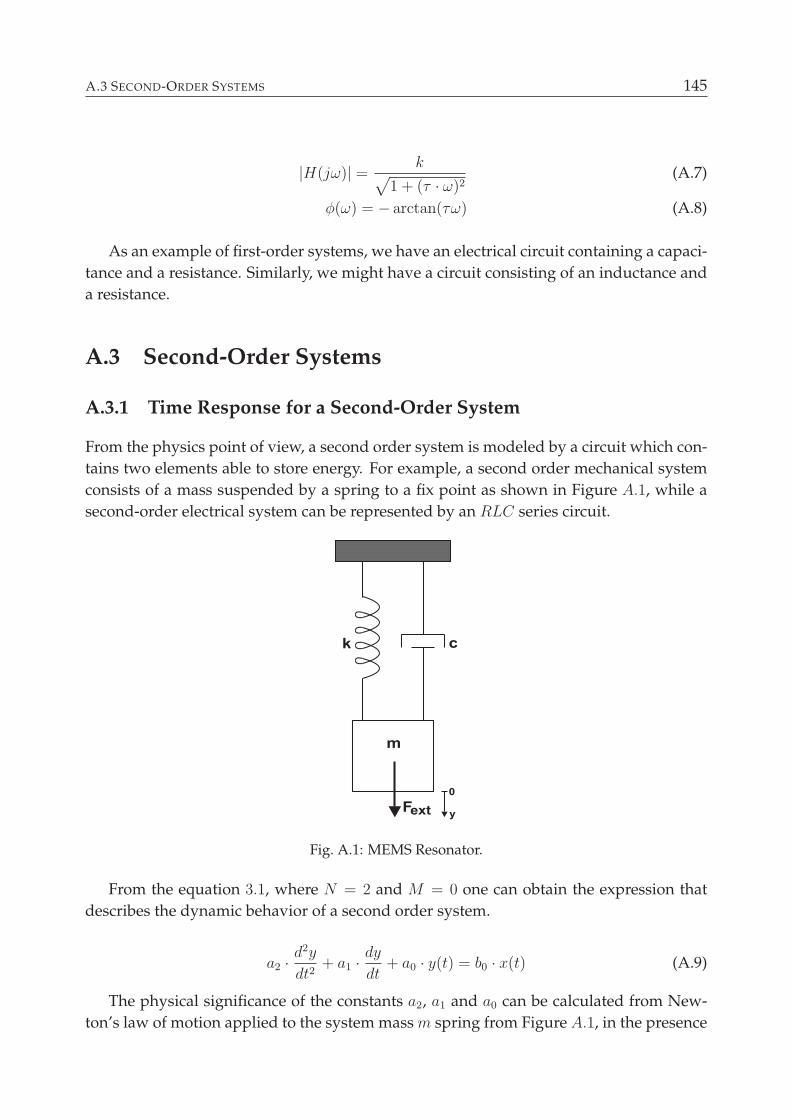
A.3 SECOND-ORDER SYSTEMS 145
|H(jω)| =k
√
1 + (τ · ω)2(A.7)
φ(ω) = − arctan(τω) (A.8)
As an example of first-order systems, we have an electrical circuit containing a capaci-
tance and a resistance. Similarly, we might have a circuit consisting of an inductance and
a resistance.
A.3 Second-Order Systems
A.3.1 Time Response for a Second-Order System
From the physics point of view, a second order system is modeled by a circuit which con-
tains two elements able to store energy. For example, a second order mechanical system
consists of a mass suspended by a spring to a fix point as shown in Figure A.1, while a
second-order electrical system can be represented by an RLC series circuit.
k
F
c
m
ext y
0
Fig. A.1: MEMS Resonator.
From the equation 3.1, where N = 2 and M = 0 one can obtain the expression that
describes the dynamic behavior of a second order system.
a2 ·d2y
dt2+ a1 ·
dy
dt+ a0 · y(t) = b0 · x(t) (A.9)
The physical significance of the constants a2, a1 and a0 can be calculated from New-
ton’s law of motion applied to the system mass m spring from Figure A.1, in the presence
146 APPENDIX A MICRO-MECHANICAL SYSTEMS
of damping force (equal to c · dy
dt), when an external force Fext acts in the y direction. Thus,
we obtain the equation from below:
m · d2y
dt2+ c · dy
dt+ k · y = Fext (A.10)
where k is the mechanical spring constant and c represents the damping coefficient.
The above equation can be written as a function of the resonant natural frequency
ω0 =√
km
, the quality factor Q = ω0mc
=√
kmc
, the critical damping coefficient cc = 2√km
and the damping ratio ξ = ccc
.
By solving the above equation, one can obtain the displacement of the inertial mass as
a function of time for different values of damping ratio as follows:
Undamped oscillatory regime : ξ = 0
y(t) = A cos(ω0t) +B · sin(ω0t) +Fext
k(A.11)
Under-damped regime : 0 < ξ < 1. In this case, the system is oscillating at a damped
natural frequency ωd = ω0 ·√
1 − ξ2 and with a decaying rate of exp(−ξω0t).
y(t) = exp(−ξω0t)(C1 cos(ω0
√
1 − ξ2t) + C2 · sin(ω0
√
1 − ξ2t)) +Fext
k(A.12)
Critically damped regime : ξ = 1. Its response makes the transition from the non-
oscillatory over-damped response to the oscillatory motion.
y(t) = (M +N · t) · exp(−ω0t) +Fext
k(A.13)
Over-damped regime : ξ > 1. The response exhibits no overshoot or oscillation.
y(t) = P exp(λ1t) +R exp(λ2t) +Fext
k(A.14)
A.3.2 Frequency Response for a Second-Order System
From the equation A.10, by applying the Laplace transform, we obtain the transfer func-
tion and its components.
H(s) =Y (s)
Fext(s)=
1/ks2
ω20
+ sQω0
+ 1(A.15)
|H(jω)| =1/k
√
(1 − ω2
ω20)2 + ( ω
Qω0)2
(A.16)
φ(ω) = − arctan(
ωQω0
1 − ω2
ω20
) (A.17)
Appendix B
Matlab Code Support for Deriving
Electrical Behavior of DG SOI MOSFET
Device Related to Gate and Drain
Voltage
The analytical modelling of a symmetric un-doped DG SOI MOSFET device has been
done in Chapter 4 from thesis and this approach started from the calculation of the Pois-
son’s equation and, then, has continued with the derivation of its electrical static and
dynamic characteristics. The entire procedure has depended on the following transcen-
dental equation:
VGS − ψ0 = a · eq(ψ0−V )
2kT · | tan(z)| − 2kT
q· lncos(z) (B.1)
from which the central silicon electrostatic potential was obtained. In this context, the
surface electrostatic potential, inversion charge, drain current, transconductance, output
conductance, terminal charges and capacitances were calculated as follows:
ψs = ψ0 −2kT
q· lncos[b · e
q(ψ0−V )2kT · tsi
2] (B.2)
Qinv =√
8εSinikT · eq(ψ0−V )
2kT ·∣
∣
∣
∣
tan(beq(ψ0−V )
2kT · tSi
2)
∣
∣
∣
∣
(B.3)
ID = µ · WL
·√
8εSinikT ·∫ VDS
0
eq(ψ0−V )
2kT ·∣
∣
∣
∣
tan(beq(ψ0−V )
2kT · tSi
2)
∣
∣
∣
∣
dV (B.4)
147
148APPENDIX B MATLAB CODE SUPPORT FOR DERIVING ELECTRICAL BEHAVIOR OF DG SOI MOSFET
DEVICE RELATED TO GATE AND DRAIN VOLTAGE
gm = 2µ · WL
· εox
tox
· [VDS − ∂
∂VGS
(
∫ VDS
0
ψs(V )dV )] (B.5)
gout = 2µ · WL
· εox
tox
· [VGS − ∂
∂VDS
(
∫ VDS
0
ψs(V )dV )] (B.6)
QG = −W∫ L
0
Qinv(y)dy = −µW 2
∫ VDS
0
Q2inv(V )
IDdV (B.7)
QD = W
∫ L
0
y
LQinv(y)dy =
WLtox
2ǫox
∫ VDS
0
Q2inv(V )
VGSV −∫ V
0ψs(v)dv
dV (B.8)
QS = QG −QD (B.9)
CKK =∂qK∂vK
|Q−point (B.10)
CKL = −∂qK∂vL
|Q−point;L 6= K (B.11)
At this point, one can see that the numerical methods must be applied in order to
obtain the dependencies of the above-mentioned coefficients as a function of gate and
drain voltages and thus, Matlab codes were used for this purpose.
The appendix has two sections where the previous electrical parameters are going
to be extracted from. Each program is providing the dependencies on gate and drain
voltages, respectively. The used notations are as follows:
- minimum electrostatic potential in the central part of silicon film: psiovf = f(VGS, VDS);
- silicon surface electrostatic potential: psis = f(VGS, VDS);
- inversion charge: Qi = f(VGS, VDS);
- drain current: Id = f(VGS, VDS);
- trans-conductance: gm = f(VGS);
- output conductance: god = f(VDS);
- terminal charges: Qg = f(VGS, VDS), Qd = f(VGS, VDS), Qs = f(VGS, VDS);
- capacitances: Cgg = f(VGS), Csg = f(VGS), Cdg = f(VGS), Cdd = f(VDS), Cgd =
f(VDS), Csd = f(VDS).
B.1 Matlab Code Support for Deriving Electrical Behavior
of DG SOI MOSFET Device Related to Gate Voltage
%%%%% The Calculation of the Silicon Central and Surface %%% %%
%%%%% Electrostatic Potentials, Inversion and Terminal %% %%%
%%%%% Charges, Drain Current, Transconductance and %%%%%
%%%%% Capacitances as a Function of Gate Voltage %%%%%
B.1 MATLAB CODE SUPPORT FOR DERIVING ELECTRICAL BEHAVIOR OF DG SOI MOSFET DEVICE
RELATED TO GATE VOLTAGE 149
%%%%%%%% Constants: %%%%%%%%
q = 1.6 * 10ˆ-19; % Electric charge [C]
k = 1.3807 * 10ˆ-23; % Boltzmann’s constant [J/K]
T = 300; % Temperature [K]
eps_o = 8.8542 * 10ˆ-12; % Vacuum permitivity [F/m]
eps_rsi = 11.7; % Relative permitivity of silicon
eps_si = eps_o * eps_rsi; % Silicon permitivity
eps_rox = 4; % Relative permitivity of $SiO_2$
eps_ox = eps_o * eps_rox; %Permitivity of $SiO_2$
t_si = 20 * 10ˆ-9; % Silicon thickness [m]
t_ox = 2 * 10ˆ-9; % Oxide thickness [m]
ni = 1.45 * 10ˆ16; % Intrinsic concentration [mˆ3]
mu = 300 * 10ˆ-4; % Electrons mobility [mˆ2/Vs]
W = 1e-6; % Channel’s width [$\mu m$]
L = 1e-6; % Channel’s length [$\mu m$]
a = t_ox/eps_ox * sqrt(2 * k* T* eps_si * ni);
b = sqrt(q * q* ni/(2 * eps_si * k* T));
const = sqrt(8 * eps_si * ni * k * T);
Qg_constant = -2 * mu * W* W;
Qd_constant = mu * mu * W* W* W/(L);
ct = mu * W/L;
Cox = eps_ox/t_ox; % Oxide capacitance per unit area
%%%%%%%% Code: %%%%%%%%
Vg=0:0.05:2; % Gate to source voltage [V]
Vds=0:0.01:1.5; % Drain to source voltage [V]
for l = 1:length(Vg)
Vgs = Vg(l);
for i = 1:length(Vds)
if (i==1)
% Calculation of psi_o for a Vds = 0 V and Riemann’s
% sum for the first iteration:
V = 0;
psi_omax_0 = V + (2 * k* T/q) * log(pi/(b * t_si)); % Maximum
% value of the silicon central electrostatic potential
psi_ox = 0:0.0001:psi_omax_0 ;
deltaVds = 0.1; % The rate for Riemann sum
150APPENDIX B MATLAB CODE SUPPORT FOR DERIVING ELECTRICAL BEHAVIOR OF DG SOI MOSFET
DEVICE RELATED TO GATE AND DRAIN VOLTAGE
for j = 1:length(psi_ox)
z = psi_ox(j);
f1(j) = Vgs - z;
g1(j) = a * exp(q * (z-V)/(2 * k* T)). * abs(tan(b * exp(q * (z-V)
/(2 * k* T)) * t_si/2))-2 * k* T/q * log(abs(cos(b * exp(q
* (z-V)/(2 * k* T)) * t_si/2)));
h1(j) = f1(j) - g1(j);
if abs(h1(j)) <= 0.05
psi_ov = z; % Minimum electrostatic potential obtained
% for the first iteration
end
end
% Drain current for the first iteration:
Id(l,i) = ct * deltaVds * exp(q * (psi_ov-V)/(2 * k* T)). * abs(tan(b
* exp(q * (psi_ov-V)/(2 * k* T)) * t_si/2)) * const;
% Silicon surface electrostatic potential for the first
% iteration:
psi_s(l,i) = psi_ov-(2 * k* T/q) * log(cos(b * exp(q * (psi_ov-V)
/(2 * k* T)) * t_si/2));
funct(l,i) = exp(q * (psi_ov-V)/(2 * k* T)). * abs(tan(b * exp(q
* (psi_ov-V)/(2 * k* T)) * t_si/2));
% Inversion charge for the first iteration:
Qi(l,i) = const * funct(l,i);
% Gate charge for the first iteration:
Qg_num(l,i) = (Vgs-psi_s(l,i)) * Qi(l,i) * deltaVds;
Qg(l,i) = Cox * Qg_num(l,i)/Id(l,i);
% Drain charge for the first iteration:
F(l,i) = Qi(l,i) * deltaVds;
Qd_num(l,i) = F(l,i) * Qi(l,i) * Qi(l,i) * deltaVds;
Qd(l,i) = Qd_num(l,i)/(Id(l,i) * Id(l,i));
% Source charge for the first iteration:
Qs1_num(l,i) = Qi(l,i) * Qi(l,i) * deltaVds;
Qs1(l,i) = Qg_constant * Qs1_num(l,i)/(2 * Id(l,i));
Qs(l,i) = Qs1(l,i) + Qd_constant * 2 * Qd(l,i);
else
t = Vds(i);
psi_omax = t + (2 * k* T/q) * log(pi/(b * t_si));
B.1 MATLAB CODE SUPPORT FOR DERIVING ELECTRICAL BEHAVIOR OF DG SOI MOSFET DEVICE
RELATED TO GATE VOLTAGE 151
psi_o = 0:0.0001:psi_omax;
for j = 1:length(psi_o)
z = psi_o(j);
f = Vgs - z;
g = a* exp(q * (z-t)/(2 * k* T)) * abs(tan(b * exp(q * (z-t)
/(2 * k* T)) * t_si/2))-2 * k* T/q * log(cos(b * exp(q
* (z-t)/(2 * k* T)) * t_si/2));
h = f - g;
if abs(h) <= 0.06
psi_ovf(l,i) = z;
V_ds(l,i)=t;
% Silicon surface electrostatic potential:
psi_s(l,i) = psi_ovf(l,i)-2 * k* T/q * log(cos(b * exp(q
* (psi_ovf(l,i)-V_ds(l,i))/(2 * k* T))
* t_si/2));
% Drain current:
funct(l,i)=exp(q * (psi_ovf(l,i)-V_ds(l,i))/(2 * k* T))
* abs(tan(b * exp(q * (psi_ovf(l,i)-V_ds(l,i))
/(2 * k* T)) * t_si/2));
Id(l,i) = Id(l,i-1)+funct(l,i) * deltaVds * const * ct;
% Inversion Charge:
Qi(l,i)= const * funct(l,i);
% Gate charge:
Qg_num(l,i) = Qg_num(l,i-1)+(Vgs-psi_s(l,i)) * Qi(l,i)
* deltaVds;
Qg(l,i) = Cox * Qg_num(l,i)/Id(l,i);
% Drain charge:
F(l,i) = F(l,i-1) + Qi(l,i) * deltaVds;
Qd_num(l,i) = Qd_num(l,i-1)+F(l,i) * Qi(l,i) * Qi(l,i)
* deltaVds;
Qd(l,i) = Qd_num(l,i)/(Id(l,i) * Id(l,i));
% Source charge:
Qs1_num(l,i) = Qs1_num(l,i-1)+Qi(l,i) * Qi(l,i) * deltaVds;
Qs1(l,i) =Qg_constant * Qs1_num(l,i)/(2 * Id(l,i));
Qs(l,i) = Qs1(l,i) + Qd_constant * Qd(l,i);
Q_g(l,i) = Qg_constant * Qg(l,i); % Gate Charge
Q_d(l,i) = Qd_constant * Qd(l,i);
end
152APPENDIX B MATLAB CODE SUPPORT FOR DERIVING ELECTRICAL BEHAVIOR OF DG SOI MOSFET
DEVICE RELATED TO GATE AND DRAIN VOLTAGE
end
end
end
Q_g = Qg_constant * Qg(:,101);
Q_d = Qd_constant * Qd(:,101);
Q_s = Qs(:,101);
end
%%%%% Capacitances %%%%%
for i=1:length(Q_g)
if ( i==1 || i==2 )
Cgg(i)=-(-Q_g(i+2)+4 * Q_g(i+1)-3 * Q_g(i))/(2 * deltaVds);
elseif( i>=3 & i<(length(Q_g)-1))
Cgg(i)=-(-Q_g(i+2)+8 * Q_g(i+1)-8 * Q_g(i-1)+Q_g(i-2))/(12 * deltaVds);
elseif (i>=length(Q_g)-1)
Cgg(i)=-(3 * Q_g(i)-4 * Q_g(i-1)+Q_g(i-2))/(2 * deltaVds);
end
end
for i=1:length(Q_d)
if ( i==1 || i==2 )
Cdg(i)=-(-Q_d(i+2)+4 * Q_d(i+1)-3 * Q_d(i))/(2 * deltaVds);
elseif( i>=3 & i<(length(Q_d)-1))
Cdg(i)=-(-Q_d(i+2)+8 * Q_d(i+1)-8 * Q_d(i-1)+Q_d(i-2))/(12 * deltaVds);
elseif (i>=length(Q_d)-1)
Cdg(i)=-(3 * Q_d(i)-4 * Q_d(i-1)+Q_d(i-2))/(2 * deltaVds);
end
end
for i=1:length(Q_s)
if ( i==1 || i==2 )
Csg(i)=-(-Q_s(i+2)+4 * Q_s(i+1)-3 * Q_s(i))/(2 * deltaVds);
elseif( i>=3 & i<(length(Q_s)-1))
Csg(i)=-(-Q_s(i+2)+8 * Q_s(i+1)-8 * Q_s(i-1)+Q_s(i-2))/(12 * deltaVds);
elseif (i>=length(Q_s)-1)
Csg(i)=-(3 * Q_s(i)-4 * Q_s(i-1)+Q_s(i-2))/(2 * deltaVds);
end
end
%%%%% Representation of figures: %%%%%
figure
plot(Vg, psi_ovf(:,1), ’-ks’, Vg, psi_s(:,1), ’-ko’,...
B.2 MATLAB CODE SUPPORT FOR DERIVING ELECTRICAL BEHAVIOR OF DG SOI MOSFET DEVICE
RELATED TO DRAIN VOLTAGE 153
’LineWidth’,1.25,...
’MarkerEdgeColor’,’k ’,...
’MarkerFaceColor’,’r’,...
’MarkerSize’,5); grid on
xlabel(’Gate voltage: V_gs(V)’);
ylabel(’Electrostatic silicon potentials (V)’);
legend(’Central silicon potential: psi_o(V)’,
’Surface silicon potential: psi_s(V)’, 2);
figure
plot(Vg, Qi(:,1), Vg, Qi(:,51), Vg, Qi(:,101), Vg, Qi(:,15 1));
grid on
legend(’V_DS = 0 V’,’V_DS = 0.5 V’,’V_DS = 1 V’,
’V_DS = 1.5 V’, 0);
xlabel(’Voltage to Source Voltage V_DS [V]’);
ylabel(’Inversion Charge Q [C]’);
figure
plot(Vg, Id);
xlabel(’Gate voltage: V_gs(V)’);
ylabel(’Electric drain current (A)’);
figure
plot(Vg, -Q_g, Vg, Q_d, Vg, -Q_s); legend(’Qg’,’Qd’,’Qs’, 0);
grid on
xlabel(’Gate to Source Voltage V_DS [V]’);
ylabel(’Terminal Charge Q [C]’);
figure
plot(Vg,Cgg/(10 * Cox* W* L), Vg,-Cdg/(10 * Cox* W* L), Vg,Csg/(10 * Cox* W* L));
legend(’C_gg’,’C_dg’,’C_sg’,0);
xlabel(’Gate to Source Potential V_GS (V)’);
ylabel(’Normalized Capacitances to C_oxWL’);
B.2 Matlab Code Support for Deriving Electrical Behavior
of DG SOI MOSFET Device Related to Drain Voltage
%%%%% The Calculation of the Silicon Central and Surface %%% %%
%%%%% Electrostatic Potentials, Inversion and Terminal %% %%%
%%%%% Charges, Drain Current, Output Conductance, and %%%% %
%%%%% Capacitances as a Function of Drain Voltage %%%%%
154APPENDIX B MATLAB CODE SUPPORT FOR DERIVING ELECTRICAL BEHAVIOR OF DG SOI MOSFET
DEVICE RELATED TO GATE AND DRAIN VOLTAGE
%%%%%%%% Constant: %%%%%%%%
q = 1.6 * 10ˆ-19; % Electric charge [C]
k = 1.3807 * 10ˆ-23; % Boltzmann’s constant [J/K]
T = 300; % Temperature [K]
eps_o = 8.8542 * 10ˆ-12; % Vacuum permitivity [F/m]
eps_rsi = 11.7; % Relative permitivity of silicon
eps_si = eps_o * eps_rsi; % Silicon permitivity
eps_rox = 4; % Relative permitivity of $SiO_2$
eps_ox = eps_o * eps_rox; %Permitivity of $SiO_2$
t_si = 20 * 10ˆ-9; % Silicon thickness [m]
t_ox = 2 * 10ˆ-9; % Oxide thickness [m]
ni = 1.45 * 10ˆ16; % Intrinsic concentration [mˆ3]
mu = 300 * 10ˆ-4; % Electrons mobility [mˆ2/Vs]
W = 1e-6; % Channel’s width [$\mu m$]
L = 1e-6; % Channel’s length [$\mu m$]
a = t_ox/eps_ox * sqrt(2 * k* T* eps_si * ni);
b = sqrt(q * q* ni/(2 * eps_si * k* T));
const = sqrt(8 * eps_si * ni * k * T);
Qg_constant = -2 * mu * W* W;
Qd_constant = mu * mu * W* W* W/(L);
ct = mu * W/L;
Cox = eps_ox/t_ox; % Oxide capacitance per unit area
%%%%%%%% Code: %%%%%%%%
Vgs = 1; % Gate to source voltage [V]
Vds = 0:0.001:2; % Drain to source voltage [V]
for i = 1:length(Vds)
if (i==1)
% Calculation of psi_o for a Vds = 0 V and Riemann’s sum for the
% first iteration:
V = 0;
psi_omax_0 = V + (2 * k* T/q) * log(pi/(b * t_si)); % Maximum value of
% the silicon central electrostatic potential
psi_ox = 0:0.0001:psi_omax_0;
deltaVds = 0.001; % The rate for Riemann sum
for j = 1:length(psi_ox)
z = psi_ox(j);
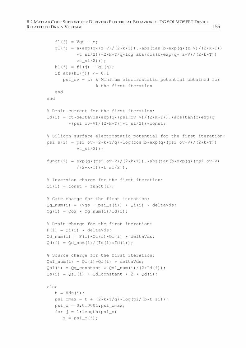
B.2 MATLAB CODE SUPPORT FOR DERIVING ELECTRICAL BEHAVIOR OF DG SOI MOSFET DEVICE
RELATED TO DRAIN VOLTAGE 155
f1(j) = Vgs - z;
g1(j) = a * exp(q * (z-V)/(2 * k* T)). * abs(tan(b * exp(q * (z-V)/(2 * k* T))
* t_si/2))-2 * k* T/q * log(abs(cos(b * exp(q * (z-V)/(2 * k* T))
* t_si/2)));
h1(j) = f1(j) - g1(j);
if abs(h1(j)) <= 0.1
psi_ov = z; % Minimum electrostatic potential obtained for
% the first iteration
end
end
% Drain current for the first iteration:
Id(i) = ct * deltaVds * exp(q * (psi_ov-V)/(2 * k* T)). * abs(tan(b * exp(q
* (psi_ov-V)/(2 * k* T)) * t_si/2)) * const;
% Silicon surface electrostatic potential for the first ite ration:
psi_s(i) = psi_ov-(2 * k* T/q) * log(cos(b * exp(q * (psi_ov-V)/(2 * k* T))
* t_si/2));
funct(i) = exp(q * (psi_ov-V)/(2 * k* T)). * abs(tan(b * exp(q * (psi_ov-V)
/(2 * k* T)) * t_si/2));
% Inversion charge for the first iteration:
Qi(i) = const * funct(i);
% Gate charge for the first iteration:
Qg_num(i) = (Vgs - psi_s(i)) * Qi(i) * deltaVds;
Qg(i) = Cox * Qg_num(i)/Id(i);
% Drain charge for the first iteration:
F(i) = Qi(i) * deltaVds;
Qd_num(i) = F(i) * Qi(i) * Qi(i) * deltaVds;
Qd(i) = Qd_num(i)/(Id(i) * Id(i));
% Source charge for the first iteration:
Qs1_num(i) = Qi(i) * Qi(i) * deltaVds;
Qs1(i) = Qg_constant * Qs1_num(i)/(2 * Id(i));
Qs(i) = Qs1(i) + Qd_constant * 2 * Qd(i);
else
t = Vds(i);
psi_omax = t + (2 * k* T/q) * log(pi/(b * t_si));
psi_o = 0:0.0001:psi_omax;
for j = 1:length(psi_o)
z = psi_o(j);
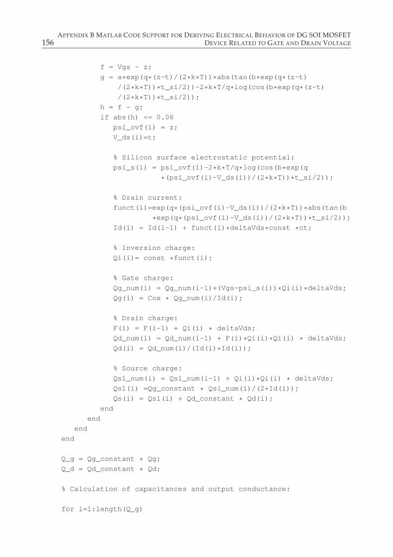
156APPENDIX B MATLAB CODE SUPPORT FOR DERIVING ELECTRICAL BEHAVIOR OF DG SOI MOSFET
DEVICE RELATED TO GATE AND DRAIN VOLTAGE
f = Vgs - z;
g = a* exp(q * (z-t)/(2 * k* T)) * abs(tan(b * exp(q * (z-t)
/(2 * k* T)) * t_si/2))-2 * k* T/q * log(cos(b * exp(q * (z-t)
/(2 * k* T)) * t_si/2));
h = f - g;
if abs(h) <= 0.06
psi_ovf(i) = z;
V_ds(i)=t;
% Silicon surface electrostatic potential:
psi_s(i) = psi_ovf(i)-2 * k* T/q * log(cos(b * exp(q
* (psi_ovf(i)-V_ds(i))/(2 * k* T)) * t_si/2));
% Drain current:
funct(i)=exp(q * (psi_ovf(i)-V_ds(i))/(2 * k* T)) * abs(tan(b
* exp(q * (psi_ovf(i)-V_ds(i))/(2 * k* T)) * t_si/2));
Id(i) = Id(i-1) + funct(i) * deltaVds * const * ct;
% Inversion charge:
Qi(i)= const * funct(i);
% Gate charge:
Qg_num(i) = Qg_num(i-1)+(Vgs-psi_s(i)) * Qi(i) * deltaVds;
Qg(i) = Cox * Qg_num(i)/Id(i);
% Drain charge:
F(i) = F(i-1) + Qi(i) * deltaVds;
Qd_num(i) = Qd_num(i-1) + F(i) * Qi(i) * Qi(i) * deltaVds;
Qd(i) = Qd_num(i)/(Id(i) * Id(i));
% Source charge:
Qs1_num(i) = Qs1_num(i-1) + Qi(i) * Qi(i) * deltaVds;
Qs1(i) =Qg_constant * Qs1_num(i)/(2 * Id(i));
Qs(i) = Qs1(i) + Qd_constant * Qd(i);
end
end
end
end
Q_g = Qg_constant * Qg;
Q_d = Qd_constant * Qd;
% Calculation of capacitances and output conductance:
for i=1:length(Q_g)
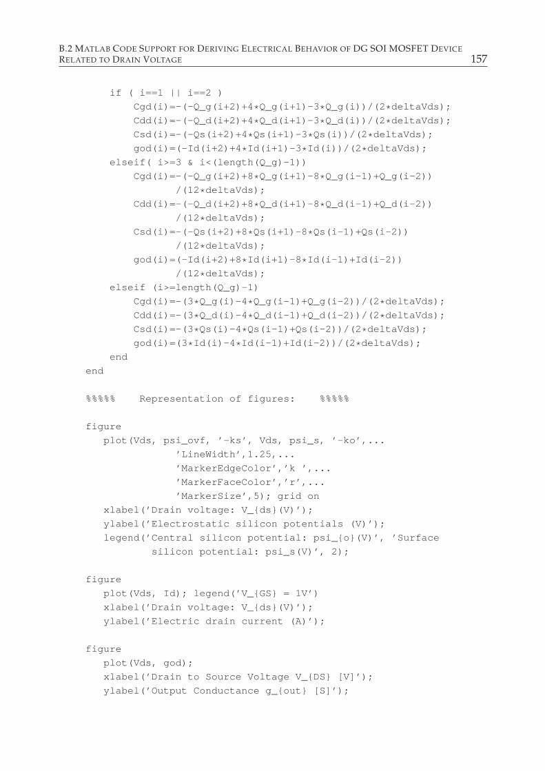
B.2 MATLAB CODE SUPPORT FOR DERIVING ELECTRICAL BEHAVIOR OF DG SOI MOSFET DEVICE
RELATED TO DRAIN VOLTAGE 157
if ( i==1 || i==2 )
Cgd(i)=-(-Q_g(i+2)+4 * Q_g(i+1)-3 * Q_g(i))/(2 * deltaVds);
Cdd(i)=-(-Q_d(i+2)+4 * Q_d(i+1)-3 * Q_d(i))/(2 * deltaVds);
Csd(i)=-(-Qs(i+2)+4 * Qs(i+1)-3 * Qs(i))/(2 * deltaVds);
god(i)=(-Id(i+2)+4 * Id(i+1)-3 * Id(i))/(2 * deltaVds);
elseif( i>=3 & i<(length(Q_g)-1))
Cgd(i)=-(-Q_g(i+2)+8 * Q_g(i+1)-8 * Q_g(i-1)+Q_g(i-2))
/(12 * deltaVds);
Cdd(i)=-(-Q_d(i+2)+8 * Q_d(i+1)-8 * Q_d(i-1)+Q_d(i-2))
/(12 * deltaVds);
Csd(i)=-(-Qs(i+2)+8 * Qs(i+1)-8 * Qs(i-1)+Qs(i-2))
/(12 * deltaVds);
god(i)=(-Id(i+2)+8 * Id(i+1)-8 * Id(i-1)+Id(i-2))
/(12 * deltaVds);
elseif (i>=length(Q_g)-1)
Cgd(i)=-(3 * Q_g(i)-4 * Q_g(i-1)+Q_g(i-2))/(2 * deltaVds);
Cdd(i)=-(3 * Q_d(i)-4 * Q_d(i-1)+Q_d(i-2))/(2 * deltaVds);
Csd(i)=-(3 * Qs(i)-4 * Qs(i-1)+Qs(i-2))/(2 * deltaVds);
god(i)=(3 * Id(i)-4 * Id(i-1)+Id(i-2))/(2 * deltaVds);
end
end
%%%%% Representation of figures: %%%%%
figure
plot(Vds, psi_ovf, ’-ks’, Vds, psi_s, ’-ko’,...
’LineWidth’,1.25,...
’MarkerEdgeColor’,’k ’,...
’MarkerFaceColor’,’r’,...
’MarkerSize’,5); grid on
xlabel(’Drain voltage: V_ds(V)’);
ylabel(’Electrostatic silicon potentials (V)’);
legend(’Central silicon potential: psi_o(V)’, ’Surfac e
silicon potential: psi_s(V)’, 2);
figure
plot(Vds, Id); legend(’V_GS = 1V’)
xlabel(’Drain voltage: V_ds(V)’);
ylabel(’Electric drain current (A)’);
figure
plot(Vds, god);
xlabel(’Drain to Source Voltage V_DS [V]’);
ylabel(’Output Conductance g_out [S]’);
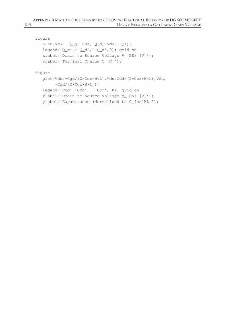
158APPENDIX B MATLAB CODE SUPPORT FOR DERIVING ELECTRICAL BEHAVIOR OF DG SOI MOSFET
DEVICE RELATED TO GATE AND DRAIN VOLTAGE
figure
plot(Vds, -Q_g, Vds, Q_d, Vds, -Qs);
legend(’Q_g’,’-Q_d’,’-Q_s’,0); grid on
xlabel(’Drain to Source Voltage V_DS [V]’);
ylabel(’Terminal Charge Q [C]’);
figure
plot(Vds,-Cgd/(2 * Cox* W* L),Vds,Cdd/(2 * Cox* W* L),Vds,
-Csd/(2 * Cox* W* L));
legend(’Cgd’,’Cdd’, ’-Csd’, 0); grid on
xlabel(’Drain to Source Voltage V_DS [V]’);
ylabel(’Capacitance (Normalized to C_oxWL)’);
Appendix C
Verilog A Description of The Static
Electrical Characteristics of an Un-doped
Symmetric DG SOI MOSFET Device
This Appendix reveals a code written in Verilog A which is capable to provide the electri-
cal behaviour of our un-doped symmetric DG SOI MOSFET . The code offers the pos-
sibility to characterize the novel device starting from the calculation of the electrostatic
potentials and continuing with the derivation of the charges, drain current, conductances
and capacitances in a similar manner with the one used in Matlab. In comparison with
Matlab code, the obtained code in Verilog A is a library that can be used in the background
of Cadence for further design of the analog and/or digital circuits. In the structure of the
Verilog A code, one can see the usage of an instruction called ”module Analyses(G,S,D)”.
Its role is to show the number of terminals of the created symbol which is used in further
simulations. Since it is about a symmetrical DG SOI MOSFET device, only three termi-
nals (gate, drain, source) are going to be utilized in the obtained symbol from Cadence in
order to describe the electrical characteristics of it.
The notations used in Verilog A code are in terms of:
- minimum electrostatic potential in the central part of silicon film: psiovf = f(VGS, VDS);
- silicon surface electrostatic potential: psis = f(VGS, VDS);
- inversion charge: Qi = f(VGS, VDS);
- drain current: Id = f(VGS, VDS);
- trans-conductance: gm = f(VGS, VDS);
- output conductance: god = f(VGS, VDS);
- terminal charges: Qg = f(VGS, VDS), Qd = f(VGS, VDS), Qs = f(VGS, VDS);
- capacitances: Cgg = f(VGS, VDS), Csg = f(VGS, VDS), Cdg = f(VGS, VDS), Cdd =
f(VGS, VDS), Cgd = f(VGS, VDS), Csd = f(VGS, VDS).
// VerilogA for DG_MOSFET, Analyses, veriloga
159
160APPENDIX C VERILOG A DESCRIPTION OF THE STATIC ELECTRICAL CHARACTERISTICS OF AN
UN-DOPED SYMMETRIC DG SOI MOSFET DEVICE
‘include "constants.h"
‘include "disciplines.h"
module Analyses(G,S,D,psio,psis,Qgd,Qdd,Qsd,CCgd,CCd d,CCsd,ggout);
inout G,S,D,psio,psis,Qgd,Qdd,Qsd,CCgd,CCdd,CCsd,ggo ut;
electrical G,S,D,psio,psis,Qgd,Qdd,Qsd,CCgd,CCdd,CCs d,ggout;
// Physical Constants:
parameter real q = 1.6e-19; // C
parameter real Eps0 = 8.854187878e-12; // F/m
parameter real Epssi = 11.7 * Eps0;
parameter real Epsox = 4 * Eps0;
parameter real ni = 1.45e16; // m-3
parameter real k = 1.380658e-23; // J/K
parameter real pi = 3.1416;
// Geometry:
parameter real W = 1e-6; // Gate Wifth [m]
parameter real L = 1e-6; // Gate Length [m]
parameter real t_ox = 2e-9; // Gate Oxide Thickness [m]
parameter real t_si = 20e-9; // Silicon Film Thickness [m]
parameter real mu = 300e-4; // Low Field Mobility [mˆ2/Vs]
parameter real Rds = 1e12; // Resistance between drain and so urce
// [Ohm] -- it is used to eliminate
// the homotopy error
// Operating Conditions:
parameter real T = 300;
parameter real V_FB = 0; // Flat-Band Voltage [V]
parameter real deltaVds = 0.001;
parameter real deltaVgs = 0.001;
// Parameters:
real vds , vgs, vd , vs , vg , psi_omax, psi_omaxm, psi_ov,
psi_ovf, psi_ox, psi_s, psi_o, psi_s1;
real f, f1, g, g1, h, h1, t, t1, z, z1, funct, funct1;
real V_ds, V1, dv_ds, max_step;
real Qi, Q_g, Qs, Q_d, Qg, Qd, Qg1, Qg2, Qd1, Qd2, Qs1, Qs2,
Qs11, Qg_num, Qd_num, Qs1_num;
real Cgd, Cdd, Csd, Cox, gout;
real a, b, const, ct, Qg_constant, Qd_constant, ix;
real Id, Id2, Id1, F1;
analog begin
161
// Derived Parameters:
a = (t_ox/Epsox) * sqrt(2.0 * k* T* Epssi * ni);
b = sqrt(q * q* ni/(2 * Epssi * k* T));
Cox = Epsox/t_ox; // Gate Oxide Capacitance
const = sqrt(8 * Epssi * ni * k * T); // without mobility and
// geometry parameters L and W
ct = mu * W/L;
Qg_constant = -2.0 * mu * W * W;
Qd_constant = mu * mu * W* W* W/(L);
psi_omaxm = (2.0 * k* T/q) * ln(pi/(b * t_si));
vd = V(D); // Drain Potential
vg = V(G); // Gate Potential
vs = V(S); // Source Potential
vds = vd-vs; // Drain to Source Voltage
vgs = vg-vs; // Gate to Source Voltage
// Thermodynamic Equilibrium:
V1=0;
for (psi_ox=0.0 ; psi_ox<=psi_omaxm ; psi_ox=psi_ox+0.00 01) begin
z1 = psi_ox;
f1 = vgs - z1;
g1= a * exp(q * (z1-V1)/(2.0 * k* T)) * abs(tan(b * exp(q * (z1-V1)
/(2.0 * k* T)) * t_si/2.0))-2.0 * k* T/q * ln(abs(cos(b * exp(q
* (z1-V1)/(2.0 * k* T)) * t_si/2.0)));
h1 = f1 - g1;
if (abs(h1) <= 0.05) psi_ov = z1;
end
psi_s1 = psi_ov-(2.0 * k* T/q) * ln(cos(b * exp(q * (psi_ov-V1)/(2.0 * k* T))
* t_si/2.0));
Id = ct * const * deltaVds * exp(q * (psi_ov-V1)/(2.0 * k* T)) * abs(tan(b
* exp(q * (psi_ov-V1)/(2.0 * k* T)) * t_si/2.0));
funct1 = exp(q * (psi_ov-V1)/(2.0 * k* T)) * abs(tan(b * exp(q * (psi_ov
-V1)/(2.0 * k* T)) * t_si/2.0));
Qi = const * funct1;
// Gate Charge Calculation:
Qg_num = (vgs - psi_s1) * Qi * deltaVds;
Qg = Cox * Qg_num/Id;
162APPENDIX C VERILOG A DESCRIPTION OF THE STATIC ELECTRICAL CHARACTERISTICS OF AN
UN-DOPED SYMMETRIC DG SOI MOSFET DEVICE
Q_g = Qg_constant * Qg;
// Drain Charge Calculation:
F1 = Qi * deltaVds;
Qd_num = F1 * Qi * Qi * deltaVds;
Qd = Qd_num/(Id * Id);
Q_d = Qd_constant * Qd;
// Source Charge Calculation:
Qs1_num = Qi * Qi * deltaVds;
Qs1 = Qg_constant * Qs1_num/(2.0 * Id);
Qs = Qs1 + Qd_constant * 2.0 * Qd;
// Thermodynamic Non-Equilibrium:
for(dv_ds=0.001; dv_ds<= vds; dv_ds=dv_ds+deltaVds) beg in
t1 = dv_ds;
psi_omax = t1 + psi_omaxm;
for (psi_o=0 ; psi_o <=psi_omax ; psi_o = psi_o+0.0001)
begin
z = psi_o;
f = vgs - z;
g = a* exp(q * (z-t1)/(2.0 * k* T)) * abs(tan(b * exp(q * (z-t1)
/(2.0 * k* T)) * t_si/2.0))-2.0 * k* T/q * ln(abs(cos(b
* exp(q * (z-t1)/(2.0 * k* T)) * t_si/2.0)));
h = f - g;
if (abs(h) <= 0.05)begin
psi_ovf = z;
V_ds=t1;
end
psi_s = psi_ovf-((2.0 * k* T)/q) * ln(cos(b * exp(q
* (psi_ovf-V_ds)/(2.0 * k* T)) * t_si/2.0));
funct = exp(q * (psi_ovf-V_ds)/(2.0 * k* T)) * abs(tan(b
* exp(q * (psi_ovf-V_ds)/(2.0 * k* T)) * t_si/2.0));
Id = Id + funct * deltaVds * const * ct;
Qi= const * funct;
// Gate Charge Calculation:
Qg_num = Qg_num + (vgs - psi_s) * Qi * deltaVds;
Qg = Cox * Qg_num/Id;
Q_g = Qg_constant * Qg;
// Drain Charge Calculation:
F1 = F1 + Qi * deltaVds;
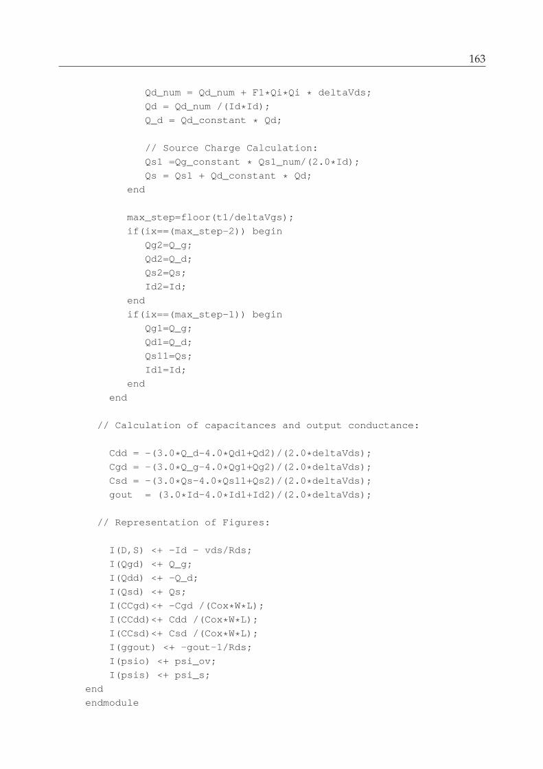
163
Qd_num = Qd_num + F1* Qi * Qi * deltaVds;
Qd = Qd_num /(Id * Id);
Q_d = Qd_constant * Qd;
// Source Charge Calculation:
Qs1 =Qg_constant * Qs1_num/(2.0 * Id);
Qs = Qs1 + Qd_constant * Qd;
end
max_step=floor(t1/deltaVgs);
if(ix==(max_step-2)) begin
Qg2=Q_g;
Qd2=Q_d;
Qs2=Qs;
Id2=Id;
end
if(ix==(max_step-1)) begin
Qg1=Q_g;
Qd1=Q_d;
Qs11=Qs;
Id1=Id;
end
end
// Calculation of capacitances and output conductance:
Cdd = -(3.0 * Q_d-4.0 * Qd1+Qd2)/(2.0 * deltaVds);
Cgd = -(3.0 * Q_g-4.0 * Qg1+Qg2)/(2.0 * deltaVds);
Csd = -(3.0 * Qs-4.0 * Qs11+Qs2)/(2.0 * deltaVds);
gout = (3.0 * Id-4.0 * Id1+Id2)/(2.0 * deltaVds);
// Representation of Figures:
I(D,S) <+ -Id - vds/Rds;
I(Qgd) <+ Q_g;
I(Qdd) <+ -Q_d;
I(Qsd) <+ Qs;
I(CCgd)<+ -Cgd /(Cox * W* L);
I(CCdd)<+ Cdd /(Cox * W* L);
I(CCsd)<+ Csd /(Cox * W* L);
I(ggout) <+ -gout-1/Rds;
I(psio) <+ psi_ov;
I(psis) <+ psi_s;
end
endmodule

Appendix D
Perturbation Method for The Analysis
and Design of Transient and Steady-State
Regimes in Electronic Oscillators
The appendix provides an asymptotic perturbation method for the analysis of the tran-
sient and steady state oscillations in the third order oscillators with shifting bias [12, 13].
In simple words, we deal with electronic oscillators, whose operation is determined by
three dominant passive components able to store energy and where the initial dc bias
voltage of the circuit is shifted by an additional stable dc voltage generated by the oscilla-
tor. In agreement with the theory of the third order systems, let us consider that they are
described by the non-linear differential equation:
N(D)x = ǫM(D)f(x) (D.1)
in which
N(D) =d3
dt3+ ǫa
d2
dt2+ b
d
dt+ ǫc (D.2)
M(D) = k2d2
dt2+ ǫk1
d
dt+ k0 (D.3)
In the relation (D.1), x is a controlling variable of the non-linear active device with its
response, f(x) (f(0) = 0), D represents the derivative operator with respect to time and ǫ
denotes the non-dimensional perturbation parameter of the oscillator, expressing circuit
losses and being given by the 1/Q, with Q as quality factor of the loop. In the above
equation, the parameters a and c are assumed to be constant while b has the following
form:
165
166APPENDIX D PERTURBATION METHOD FOR THE ANALYSIS AND DESIGN OF TRANSIENT AND
STEADY-STATE REGIMES IN ELECTRONIC OSCILLATORS
b(ǫ) = b0 + b1ǫ+ b2ǫ2 + ... (D.4)
b0 = 1 (D.5)
This perturbation method allows us to develop a behavioral time-domain analytical
model that describes both the transient and the steady state regime of the circuit response,
and thus to obtain a straightforward design methodology for deriving the start-up dura-
tion, the stabilized frequency and amplitude values. The advantage of the method con-
sists in the fact that the oscillation solution can be built iteratively to the degree of accu-
racy required by the application, by increasing the order of approximation from the first
order to higher orders of ǫ, and also considering not only the fundamentals but also supe-
rior harmonic components, when needed. Thus, in a generic form, the oscillator solution
can be written as follows:
x(t, ǫ) = B(t, ǫ) + A(t, ǫ)cos(ν) + ǫh(ν, ǫ) (D.6)
dν
dt= ω (D.7)
where B is the dc component, A is the amplitude of the fundamental harmonic, h is
the content of superior harmonics, and ω is the angular frequency. The essence of the
approach is that all these solution elements (B,A, ω) are written in the form of power
series as a function of perturbation parameter, ǫ.
Within this perturbation approach, the method of complex amplitudes is used, where
a time-domain oscillation solution written in the imaginary space is forced for the equa-
tion (D.1) and finally the real solution is extracted as follows:
x(ν, ǫ) = Re[B + Aejν +∑
m
Hmejmν ] (D.8)
where
B = B0 +B1ǫ+B2ǫ2 + ... (D.9)
A = A0 + A1ǫ+ A2ǫ2 + ... (D.10)
Hm = Hm,1ǫ+Hm,2ǫ2 + ... (D.11)
and
ν =
∫ t
0
ωdt (D.12)
τ = ǫt (D.13)
ω = ω0 + ω1ǫ+ ω2ǫ2 + ... (D.14)
167
One can remark that the coefficients of the power series in ǫ for A,B,Hm and ω are
considered to be functions of the slow variable τ = ǫt. This means that the time derivative
should be carefully performed for solving the equation (D.1) with the proposed solution
(D.8). For example, dωdt
= dωdτ
dτdt
= ǫdωdτ
. Further, the appendix deals with the calculation of
the complete solution of the equation (D.1) in the form of (D.8).
The complex function f(x) can be also written as a power series expansion and it has
the following form:
f(x) = f(x0 + ǫx1 + ǫ2x2 + ...) = f0 + ǫf1 + ǫ2f2 + ... (D.15)
where the real coefficients fn are 2π periodic in the variable ν and developed as Fourier
series:
fn = Re[F0,n(τ) + F1,n(τ)ejν +∑
m>2
Fm,n(τ)ejmν ], n > 0 (D.16)
Fm,n =1
π
∫ 2π
0
fne−jνdν (D.17)
F0,n =1
2π
∫ 2π
0
fndν (D.18)
The last above two relations are based on the supposition that the functions fn and
fne−jν do not significantly change in τ .Thus, f(x) in the real domain becomes:
f(x) = Re[F0 + F1ejν +
∑
m>2
Fmejmν ] (D.19)
where
F0 = F0,0 + F0,1ǫ+ F0,2ǫ2 + ... (D.20)
F1 = F1,0 + F1,1ǫ+ F1,2ǫ2 + ... (D.21)
Fm = Fm,0 + Fm,1ǫ+ Fm,2ǫ2 + ... (D.22)
At the end of this entire analysis, one can see that the Equation (D.1) can be rearranged
as follows:
N(D)[B(τ)+A(τ)ejν +∑
m>2
Hm(τ)ejmν ] = ǫM(D)[F0(τ)+F1(τ)ejν +
∑
m>2
Fm(τ)ejmν ] (D.23)
After performing all the described calculations, within the perturbation method, the
solution of the third order oscillators with shifting bias can be derived for any order of
168APPENDIX D PERTURBATION METHOD FOR THE ANALYSIS AND DESIGN OF TRANSIENT AND
STEADY-STATE REGIMES IN ELECTRONIC OSCILLATORS
approximation and harmonics as needed. Thus, the final form of equation (D.1) can be
obtained by equating the right members of the equations from below:
N(D)[B(τ) + A(τ)ejν +∑
m>0
Hm(τ)ejmν ] = ǫ3[d3B(τ)
dτ 3+ a
d2B(τ)
dτ 2
+ejν(d3A(τ)
dτ 3+ a
d2A(τ)
dτ 2) +
∑
m>2
ejmν(d3Hm(τ)
dτ 3+ a
d2Hm(τ)
dτ 2)]
+ǫ2[ejν(3jωd2A(τ)
dτ 2+ (2ajω + 3j
dω(τ)
dτ)dA(τ)
dτ+ j
d2ω(τ)
dτ 2A(τ))
+∑
m>2
ejmν(3jmωd2Hm(τ)
dτ 2+ (2ajmω + 3jm
dω(τ)
dτ)dHm(τ)
dτ+ jm
d2ω(τ)
dτ 2Hm(τ))]
+ǫ[bdB(τ)
dτ+ cB(τ) + ejν((3j2ω2 + b)
dA(τ)
dτ+ (3j2ω
dω(τ)
dτ+ aj2ω2)A(τ) + cA(τ))
+∑
m>2
ejmν((3j2m2ω2 + b)dHm(τ)
dτ+ (3j2m2ω
dω(τ)
dτ+ aj2m2ω2)Hm(τ) + cHm(τ))]
+(j3ω3A(τ) + bjωA(τ) +∑
m>2
(j3m3ω3Hm(τ) + bjmωHm(τ))) (D.24)
ǫM(D)∑
m>0
(Fmejmν) =
∑
m>0
ejmν [ǫ3(k2d2Fm(τ)
dτ 2+ k1
dFm(τ)
dτ) + ǫ2(2k2jmω
dFm(τ)
dτ
+k2jmdω(τ)
dτ+ k1jmω) + ǫ(k0 − k2m
2ω2)] (D.25)
One can remark that the initial behavioral third-order differential equation written in
the time domain, t, was translated to a time domain differential third order equation as a
function of slow time, τ , where τ = ǫt.
The above equation can take different forms as a function of desired values for ǫ and
m, i.e, respectively, the order of approximation (power of ǫ terms) and the harmonics re-
quired. Further, the zero, first order and second approximations are going to be explained
in detail.
D.1 Zero-order Approximation
According to the zero-order approximation, the perturbation parameter ǫ is zero and the
coefficients used in the relation (D.1) are the following:
D.2 FIRST-ORDER APPROXIMATION 169
B(τ) = B0(τ) (D.26)
A(τ) = A0(τ) (D.27)
Hm(τ) = 0 (D.28)
F0(τ) = F0,0(τ) (D.29)
F1(τ) = F1,0(τ) (D.30)
b = b0 (D.31)
ω = ω0 (D.32)
and the final equation (D.1) becomes:
jω0(b0 − ω20)A0e
jν = 0 (D.33)
From the above expression, we get:
b0 = ω20 (D.34)
ω0(τ) = 1 (D.35)
The last equation should be interpreted like this: In an ideal system (without losses,
ǫ = 0), the fundamental frequency is the only present component during the transient
regime, and its value cannot be changed. Actually, for non-ideal, realistic system (with
losses and where ǫ 6= 0), the fundamental harmonic will be perturbed as shown by the
results obtainedfor the higher order of approximations.
D.2 First-order Approximation
In order to analyze the first order approximation, only the terms with zero power of
epsilon and those with first power of epsilon will be used. With this condition, the terms
of the overall equation (D.1) will take the following form:
B(τ) = B0(τ) +B1(τ)ǫ (D.36)
A(τ) = A0(τ) + A1(τ)ǫ (D.37)
Hm(τ) = Hm,1(τ)ǫ (D.38)
F0(τ) = F0,0(τ) + F0,1(τ)ǫ (D.39)
F1(τ) = F1,0(τ) + F1,1(τ)ǫ (D.40)
b = b0 + b1ǫ (D.41)
ω = ω0 + ω1ǫ (D.42)
170APPENDIX D PERTURBATION METHOD FOR THE ANALYSIS AND DESIGN OF TRANSIENT AND
STEADY-STATE REGIMES IN ELECTRONIC OSCILLATORS
At this point, both dc component and fundamental harmonic can be calculated. So
that, when m = 0, the time dependence of the dc component is given by the following
differential equation:
b0dB0
dτ+ cB0 = k0F0,0 (D.43)
while, for m = 1, the (slow) time dependence of the amplitude A0 of the fundamental
harmonic can be derived from the equation (D.1), as follows:
ejν(−3ω2dA0
dτ− 3ω
dω
dτA0 − jω3A1 − aω2A0 + b0
dA0
dτ+ jωb0A1 + jωb1A0 + cA0)
+b0dB0
dτ+ cB0 = ejν(k0 − k2ω
2)F1,0 + k0F0,0 (D.44)
and the differential equation of the fundamental harmonic differential equation is:
−2ω20
dA0
dτ+ (c− aω2
0)A0 = (k0 − k2ω20)F1,0 (D.45)
By arranging the relations (D.43) and (D.45), a system of non-linear first-order differ-
ential equations in τ are derived and, thus B0(τ) and A0(τ) can be determined:
dB0
dτ= −c(B0 + k0cF0,0) (D.46)
dA0
dτ=c
2[k0c(1 − k20)F1,0 − pA0] (D.47)
where b0 = ω20 = 1, k0c = −k0
c, k20 = k2
k0and p = a
c− 1.
If m > 1, the higher harmonics amplitudes for the first order approximation are going
to be obtained as follows:
Hm,1 = jk0 − k2m
2
m(m2 − 1)Fm,0 (D.48)
One can remark the non-linearity property of the above first-order differential equa-
tions in B0 and A0, characterizing respectively the time evolution of the dc component
and the fundamental harmonic of the oscillator within its first order approximation. The
bottom line of the entire oscillator operation is the fact that, when powered ON (at t = 0),
the system should be in unstable equilibrium state (B0 = A0 = 0). If it is well designed,
it will evaluate toward an equilibrium stable state (B∗0 6= 0, A∗
0 6= 0) established at the
end of this so-called start-up time. Therefore, the design of the third order oscillator with
shifting bias described by the first order approximation should arise from imposing to
the above first-order differential equation system in A0 and B0 to be unstable in the time
D.2 FIRST-ORDER APPROXIMATION 171
origin and stable at the steady state, after the start up time (when the so-called limit cycle
is reached). Fortunately, Lyapunov has developed the mathematical background of sta-
bility for the systems described by the non-linear first order differential equation system.
Here, we have to understand that if the equation system is stable then the physical sys-
tem (in our case the oscillator) described by those equations is stable. Actually, Lyapunov
stated that if the linearized system derived from a non-linear system is stable, then the
initial non-linear system is also stable. Similarly, if the linearized equation system derived
from a non-linear equation system is unstable, then the initial non-linear equation system
is unstable. Lyapunov’s first method is also saying that a linearized differential equa-
tion system is stable if the eigenvalues of the Jacobian matrix associated to the linearized
equation system are either negative or with negative real parts. This condition of nega-
tive eigenvalues should be applied for the deriving the stable values of the dc component
and fundamental amplitude of the oscillator. Similarly, according to this first method of
Lyapunov, if the eigenvalues of the Jacobian matrix of the linearized equation system are
either positive or with real parts, then the equation system is unstable, and so it is the
physical system (in our case the oscillator). This condition of positive eigenvalues of Ja-
cobian matrix of the linearized equation system should be applied for forcing unstable
condition for oscillator at t=0.
Therefore, as per Lyapunov first stabilization method, all we have to do for the deriva-
tion of the stability and instability conditions for our oscillator is:
1. The linearization of equations (D.46) and (D.47) around the steady state values of
(A∗0, B
∗0) and around the values A0 = 0, B0 = 0;
2. The extraction of Jacobian matrix from the linearized equations obtained in the pre-
vious step;
3. The extraction of the characteristic polynomial equation of the Jacobian matrix;
4. The implementation of the stability conditions (Lyapunov’s first method);
5. The implementation of the instability conditions (Lyapunov’s first method).
Linearization principle:
The above two non-linear differential equations can be easily linearized by expanding
the two functions F0,0 and F1,0 as power series over the two values mentioned above (B0 =
A0 = 0, specific to time origin and A∗0 and B∗
0 specific to steady state) and eliminating
higher order terms. Thus, the linearized expressions for F0,0 and F1,0 are as follows
F0,0 = F0,0(A0, B0) +∂F0,0
∂B0
B0 +∂F0,0
∂A0
A0 (D.49)
F1,0 = F1,0(A0, B0) +∂F1,0
∂B0
B0 +∂F1,0
∂A0
A0 (D.50)
172APPENDIX D PERTURBATION METHOD FOR THE ANALYSIS AND DESIGN OF TRANSIENT AND
STEADY-STATE REGIMES IN ELECTRONIC OSCILLATORS
By introducing the equations (D.49) and (D.50) in the equations (D.43) and (D.44) and
by assuming that F0,0 = F1,0 = 0 (actually these neglected terms are not considered for
the calculation of the Jacobian matrix), the system of equations (D.43) and (D.44) leads to:
dB0
dτ= (k0
∂F0,0
∂B0
− c)B0 + k0∂F0,0
∂A0
A0 (D.51)
dA0
dτ=
1
2(k2 − k0)
∂F1,0
∂B0
B0 +1
2[(k2 − k0)
∂F1,0
∂A0
+ (c− a)]A0 (D.52)
The extraction of the Jacobian matrix:
Having the linearized equations, the Jacobian matrix (x = Jx) results in the form of:
J =
(
A11 A12
A21 A22
)
where A11 =ddB0dτ
dB0performed in the above (D.51) equation and thus, A11 = k0
∂F0,0
∂B0− c,
A12 = k0∂F0,0
∂A0, A21 = 1
2(k2 − k0)
∂F1,0
∂B0and A22 = 1
2(k2 − k0)
∂F1,0
∂A0.
In our case the Jacobian matrix is a 2x2 matrix.
The extraction of the characteristic polynomial equation of the Jacobian matrix
The characteristic polynomial Pj is obtained by calculating the determinant of the ma-
trix M = (J − λI2), i.e. Pj = det(J − λI2), where J is the above Jacobian matrix and
I2 is the unity matrix of 2x1 elements. By doing the calculations, the matrix M becomes
M =
(
A11 − λ A12
A21 A22 − λ
)
.
Thus the characteristic polynomial is obtained as a second-order algebra equation
from below:
Pj = λ2 − λ(A11 + A22) + (A11A22 − A12A21) (D.53)
By solving the equation Pj = 0 one can obtain the eigenvalue of the Jacobian matrix
for the linearized first-order differential equation system, as shown below:
λ2 − λ(A11 + A22) + (A11A22 − A12A21) = 0 (D.54)
For this equation, the determinant and the solutions are calculated as follows:
∆ = A211 + A2
22 − 2A11A22 + 4A12A21 (D.55)
λ1,2 =A11 + A22 ±
√∆
2(D.56)
The implementation of the stability condition (Lyapunov’s first method)
D.2 FIRST-ORDER APPROXIMATION 173
As already presented up to now, the condition for the above system of the linear- first-
order equation to be stable (which applies also for the non-linear first-order system as
demonstrated by Lyapunov) is that the above eigenvalues to be real and negative. As
the eigenvalues are the solutions of the simple algebra equation of the second order, this
translates to the following conditions from below
λ1 + λ2 < 0 (D.57)
λ1 · λ2 > 0 (D.58)
∆ > 0 (D.59)
If we take into considerations the expressions for the matrix elements A11, A12, A21,
A22, then the above stability conditions (around A∗0 and B∗
0 as defined above) become as
follows:
k0∂F0,0
∂B0
+k2 − k0
2
∂F1,0
∂A0
− c+ a
2< 0 (D.60)
(k0∂F0,0
∂B0
− c)(k2 − k0
2
∂F1,0
∂A0
+c− a
2) > k0
k2 − k0
2
∂F0,0
∂A0
· ∂F1,0
∂B0
(D.61)
Therefore the circuit elements of the third order oscillator with shifting bias should
follow the above conditions to get the oscillation stability around A∗0 and B∗
0 , becoming
thus the steady state values of the oscillation.
For those circuit values (passive components as well as active device parameters) that
obey the stability and instabilities conditions from above, the system of equations (D.46)
and (D.47) can be solved (in most of the cases numerically) and thus provide the A0 and
B0 dependencies as function of time, from the zero time till the steady state is reached.
Finally the envelopes of the oscillation solution is obtained by representing B0(τ) +A0(τ)
and B0(τ) − A0(τ) as functions of time. These envelopes are shown on a real case in the
Chapter 5.
The implementation of the instability conditions (Lyapunov’s first method)
As described above, a well designed oscillator should be unstable at the initial mo-
ment when the power supply is set ON. Therefore, an instability condition should be
”forced” at t = 0 at the design level so, that the initial small (noise) oscillating signal to
grow continuously till the steady state is reached. By opposition to the stability condi-
tion, if the eigenvalues are positive then the oscillation is unstable. This is the condition
we need to push at t=0 for our oscillator. Starting from the characteristic polynomial,
again, the instability condition becomes.
174APPENDIX D PERTURBATION METHOD FOR THE ANALYSIS AND DESIGN OF TRANSIENT AND
STEADY-STATE REGIMES IN ELECTRONIC OSCILLATORS
λ1 + λ2 > 0 (D.62)
∆ > 0 (D.63)
By introducing the explicit values of the matrix M we get the following instability
condition for our oscillator:
k0∂F0,0
∂B0
+k2 − k0
2
∂F1,0
∂A0
− c+ a
2> 0 (D.64)
(k0∂F0,0
∂B0
− c)(k2 − k0
2
∂F1,0
∂A0
+c− a
2) > k0
k2 − k0
2
∂F0,0
∂A0
· ∂F1,0
∂V0
(D.65)
D.3 Second-order Approximation
The first order approximation is all you need for the practical design considerations in
the case of third order oscillators. However, as in many practical cases, for the first order
approximation, the term ω1 expressing the deviation of the real resonant frequency from
the resonant frequency of the ideal system (ǫ = 0) is showing the value b1 = 0, then for
the study and for the analysis of the frequency shift in the real oscillating systems, the
second order approximation is needed.
In order to analyze the second order approximation, only the terms up to the second
order ǫ2, inclusive, are going to be used for B(τ), A(τ), Hm(τ), F0,n(τ), F1,n(τ), b and ω.
With this condition, the terms of the overall equation (D.1) will take the following forms:
B(τ) = B0(τ) +B1(τ)ǫ+B2(τ)ǫ2 (D.66)
A(τ) = A0(τ) + A1(τ)ǫ+ A2(τ)ǫ2 (D.67)
Hm(τ) = Hm,1(τ)ǫ+Hm,2(τ)ǫ2 (D.68)
F0,n(τ) = F0,0(τ) + F0,1(τ)ǫ+ F0,2(τ)ǫ2 (D.69)
F1,n(τ) = F1,0(τ) + F1,1(τ)ǫ+ F1,2(τ)ǫ2 (D.70)
b = b0 + b1ǫ+ b2ǫ2 (D.71)
ω = ω0 + ω1ǫ+ ω2ǫ2 (D.72)
As shown in [12], for the second order approximation analysis the following form for
the Fourier coefficients Fm,n is used:
Fm,n = KAmAn(τ) +KB
mAn(τ) +Rm,n(τ) (D.73)
D.3 SECOND-ORDER APPROXIMATION 175
where
Ck
dτ=
1
2π
∫ 2π
0
df(x)
dx|x=B0+A0cos(ν)cos(kν)dν (D.74)
KAm =
Cm−1
dτ+Cm+1
dτ(D.75)
KBm = 2
Cm
dτ(D.76)
Rm,n(τ) = RHm,n(τ) +RX
m,n(τ) (D.77)
RHm,n(τ) =
∞∑
s>2
[(Cm−s
dτ+Cm+s
dτ)ReHs,n + j(
Cm−s
dτ− Cm+s
dτ)ImHs,n] (D.78)
RXm,n(τ) =
1
π
∫ 2π
0
(∑
l1...ln−1
xl11 x
l21 ...x
ln−1
n−1
l1!l2!...ln−1!(x0))e
−jmνdν (D.79)
In this context, the solution for the second order approximation can be obtained for
each m value, starting from m = 0 (dc component) till any higher order harmonics. So
that, for m = 0 the obtained solution is:
ω20
dB1
dτ+ [c− k0K
B0 ]B1 − k0K
A0 A1 = k0R
H0,1 (D.80)
When m = 1, we get a solution with two components because of the presence of the
real and imaginary terms in the second approximation equation:
−2ω20
dA1
dτ− [(k0−k2ω
20)K
B1 ]B1 +[c−aω2
0 − ((k0−k2ω20)K
A1 )]A1 = (k0−k2ω
20)ReR
H1,1 (D.81)
2A0ω20ω2 = −(k0 − k2ω
20)ImR
H1,1 − k1ω0F1,0 − 2k2ω0
dF1,0
dτ+ A0b2ω0 + 3ω0
d2A0
dτ 2
+2aω0dA0
dτ(D.82)
For m > 1, we get a solution by considering the following equation:
m(m2 − 1)ω30Hm,2 = j(k0 − k2m
2ω20)Fm,1 − k1mω0Fm,0 − 2mω0k2
dFm,0
dτ+j(am2ω2
0 − c)Hm,1 + j(3m2 − 1)ω20Hm,1 (D.83)
176APPENDIX D PERTURBATION METHOD FOR THE ANALYSIS AND DESIGN OF TRANSIENT AND
STEADY-STATE REGIMES IN ELECTRONIC OSCILLATORS
It worths to notice, that the equation (D.82) contains a term ω2 which represents the
deviation of the resonance frequency from the natural resonance frequency of the system.
One can see that it varies in time after the equation written below:
ω2 =1
2A0
[(k2 − k0)Im(R1,1) − k1F1,0 + b2A0 − 2k2dF1,0
dτ+ 3
d2A0
dτ 2] (D.84)
Consequently, the current appendix has presented an accurate perturbation method
for the analysis and the design of the non-linear third order oscillator with shifting bias.
The quasi analytical methodology described here has the advantage of constructing an
iterative oscillator solution where the transient time, the steady state regime and the
harmonic content of the oscillating solution can be evinced. The oscillator solution is
obtained very accurately from the first order approximation approach, where the Lya-
punov’s stability method is used for identifying and designing the conditions for oscilla-
tor instability at the time origin and, respectively, the conditions for stability at the steady
state. From the system of equation characterizing the first order approximation, the time
dependence of the envelopes of oscillation is deduced. The system resonance frequency
is also obtained as a perturbation of the natural resonance frequency. The accurate devia-
tion of the real resonance frequency from the ideal value (given by the natural resonance
frequency of the feed-back loop circuit) can be derived by using the second order approx-
imation calculations.
References
[1] http://www.sitime.com/products/sit8002.php.
[2] M. A. ABDELMONEUM, M. U. DEMIRCI, and C. T.-C. NGUYEN. Stemless wine-glass-mode disk
micromechanical resonators. IEEE The Sixteenth Annual International Conference on Micro
Electro Mechanical Systems, pages 698–701, Jan. 19-23 and 2003.
[3] M. AGOSTINELLI, M. ALIOTO, D. ESSENI, and L. SELMI. Trading off static power and dynamic
performance in cmos digital circuits: Bulk versus double gate soi mosfets. 37th European
Solid State Device Research Conference, pages 191–194, 2007.
[4] A. ALLAN, D. EDENFELD, W. H. J. JR., A. B. KAHNG, M. RODGERS, and Y. ZORIAN. 2001 tech-
nology roadmap for semiconductor. IEEE Computer, 35:42–53, 2002.
[5] X. BAIE, J. COLINGE, V. BAYOT, and E. GRIVEI. Quantum-wire effects in thin and narrow soi
mosfets. Proceedings of IEEE International SOI Conference, pages 66–67, 1995.
[6] F. BALESTRA, S. CRISTOLOVEANU, M. BENACHIR, J. BRINI, and T. ELEWA. Double-gate silicon-
on-insulator transistor with volume inversion: A new device with greatly enhanced perfor-
mance. IEEE Electron Device Letters, EDL-8:410–412, 1987.
[7] A. A. BERLIN. Distributed mems: New challenges for computation. IEEE Computational
Science & Engineering, pages 12–16, 1997.
[8] A. D. BERNY. Analysis and Design of Wideband LC V COs. PhD thesis, University of Cali-
forniy, Berkeley, 2006.
[9] S. BORKAR. Obeying moore’s law beyond 0.18 micron. Proceedings of 13th Annual IEEE
International ASIC/SOC Conference, pages 26–31, 2000.
[10] A. BREED and K. ROENKER. Dual-gate (finfet) and trigate mosfets: Simulation and design.
Proceedings of the International Semiconductor Device Research Symposium, pages 150–151, 2003.
[11] W. F. BRINKMAN, D. E. HAGGAN, and W. W. TROUTMAN. A history of the invention of the
transistor and where it will lead us. IEEE Journal of Solid-State Circuits, 32:1858–1865, 1997.
[12] A. BUONOMO and A. L. SCHIAVO. A method for analysing the transient and the steady-state
oscillations in third-order oscillators with shifting bias. International Journal of Circuit Theory
and Applications, 29:469–486, 2001.
[13] A. BUONOMO and A. L. SCHIAVO. Analyzing the dynamic behavior of rf oscillators. IEEE
Transactions on Circuits and Systems - I: Fundamental Theory and Applications, 49:1525–1534,
2002.
[14] P. J. BURKE. Carbon nanotube devices for ghz to thz applications. Proceeding of SPIE,
5593:52–61, 2004.
[15] J. M. BUSTILLO, R. T. HOWE, and R. S. MULLER. Surface micromachining for microelectrome-
chanical systems. Proceedings of IEEE, 86:1552–1574, 1998.
177
178 REFERENCES
[16] T. CHAN, J. CHEN, P. KO, and C. HU. The impact of gate-induced drain leakage current on
mosfet scaling. International Electron Devices Meeting, pages 718–721, 1987.
[17] L. CHANG, Y.-K. CHOI, D. HA, P. RANADE, S. XIONG, J. BOKOR, C. HU, and T.-J. KING. Ex-
tremely scaled silicon nano-cmos devices. Proceedings of the IEEE, 91:1860–1873, 2003.
[18] L. CHANG, Y.-K. CHOI, J. KEDZIERSKI, N. LINDERT, P. XUAN, J. BOKOR, C. HU, and T.-J. KING.
Moore’s law lives on. IEEE Circuits & Devices Magazine, 19:35–42, 2003.
[19] R. CHAU, B. DOYLE, S. DATTA, J. KAVALIEROS, and K. ZHANG. Integrated nanoelectronics for
the future. Nature Materials, 6:810–812, 2007.
[20] Q. CHEN, K. A. BOWMAN, E. M. HARRELL, and J. D. MEINDL. Double jeopardy in the
nanoscale court? IEEE Circuits & Devices Magazine, pages 28–34, 2003.
[21] J. R. CLARK, W.-T. HSU, M. A. ABDELMONEUM, and C. T.-C. NGUYEN. High-q uhf microme-
chanical radial-contour mode disk resonators. Journal of Microelectromechanical Systems,
14:1298–1310, 2005.
[22] O. COBIANU and M. GLESNER. A computationally efficient method for analytical calculation
of potentials in undoped symmetric dg soi mosfet. Technical Proceedings of NSTI Nanotech-
nology Conference and Trade Show, 3(5):544–553, May 2006.
[23] O. COBIANU and M. GLESNER. Results and limits in the 1-d analytical modeling for the
asymmetric dg soi mosfet. Advances in Radio Science, 6:151–155, 2008.
[24] O. COBIANU and M. GLESNER. Asymmetric effects in an undoped symmetric dg soi mosfet
in the presence of an applied channel voltage. In 4th International Workshop on Compact
Modeling (IWCM), Pacifico Yokohama, Yokohama, Japan, 23 Jan., 2007.
[25] O. COBIANU, O. SOFFKE, and M. GLESNER. A verilog-a model of an undoped symmetric
dual-gate mosfet. Advances in Radio Science, 4(2):303–306, Apr. 2006.
[26] J.-P. COLINGE. Multiple-gate soi mosfets. Solid State Electronics, 48:897–905, 2004.
[27] J.-P. COLINGE. Silicon-On-Insulator Technology: Materials to VLSI and 3rd Edition. Springer,
Norwell and Massachusetts, 2004.
[28] J.-P. COLINGE. From gate-all-around to nanowire mosfets. Proceeding of IEEE, 2007.
[29] S. CRISTOLOVEANU. Silicon on insulator technologies and devices: from present to future.
Solid State Electronics, 45:1403–1411, 2001.
[30] S. CRISTOLOVEANU. How many gates do we need in a transistor. Proceeding of IEEE, 2007.
[31] R. DEHGHANI and S. ATARODI. Design of an optimised 2.5 ghz cmos differential lc oscillator.
IEEE Proceedings of Microwave Antennas Propagation, 151:167–172, 2004.
[32] M. U. DEMIRCI and C. T.-C. NGUYEN. Higher-mode free-free beam micromechanical res-
onators. Proceedings of the IEEE International Ultrasonics and Ferroelectrics and Frequency Con-
trol Symposium and PDA Exhibition Jointly with the 17th European Frequency and Time Forum,
pages 810–818, 2003.
[33] M. U. DEMIRCI and C. T.-C. NGUYEN. A low impedance vhf micromechanical filter using
coupled-array composite resonators. The 13th International Conference on Solid-State Sensors
and Actuators and Microsystems, 2:2131–2134, June 5–9 and 2005.
[34] M. M. DRISCOLL and D. J. HEALEY. Voltage-controlled crystal oscillators. IEEE Transactions
on Electron Devices, ED-18:528–535, 1971.
[35] O. H. ELIBOL. The double gate mosfet. EE612 Spring 2003 Final Project, pages 1–10, 2003.
REFERENCES 179
[36] T. ERNST, S. CRISTOLOVEANU, G. GHIBAUDO, T. OUISSE, S. HORIGUCHI, Y. ONO, Y. TAKAHASHI,
and K. MURASE. Ultimately thin double-gate soi mosfets. IEEE Transactions on Electron
Devices, 50:830–838, 2003.
[37] ESMART. Mems. Technical report, University of Alberta, Canada.
[38] D. FRANK, S. LAUX, and M. FISCHETTI. Monte carlo simulation of 30 nm dual-gate mosfet:
How short can si go? IEDM, 92:553–556, 1992.
[39] D. J. FRANK, R. H. DENNARD, E. NOWAK, P. M. SOLOMON, Y. TAUR, and H.-S. P. WONG. Device
scaling limits of si mosfets and their application dependencies. Proceedings of the IEEE,
89:259–288, 2001.
[40] D. J. FRANK and Y. TAUR. Design considerations for cmos near the limits of scaling. Solid
State Electronics, 46:315–320, 2002.
[41] K. J. GABRIEL. Microelectromechanical systems (mems) tutorial. IEEE International Test Con-
ference, 17:432–441, 1998.
[42] W. HAENSCH, E. NOWAK, R. DENNARD, P. SOLOMON, A. BRYANT, O. DOKUMACI, A. KUMAR,
X. WANG, J. JOHNSON, and M. FISCHETTI. Silicon cmos devices beyond scaling. IBM Journal
Res. & Dev., 50:339–361A, 2006.
[43] S. HAMILTON. Taking moore’s law into the next century. IEEE Computer, 32:43–48, 1999.
[44] J. HE, W. BIAN, Y. TAO, F. LIU, B. LI, X. ZHANG, W. WU, K. LU, T. WANG, T. Y. MAN, and
M. CHAN. Generic carrier-based approach to develop compact models of non-classical cmos
devices. IWCM, Yokohama, Japan, pages 73–81, 2007.
[45] T. HORI. Gate Dielectrics and MOS ULSIs ? Principles and Technologies and Applications.
Springer, Norwell and Massachusetts, 1997.
[46] W.-T. HSU. Vibrating rf mems for timing and frequency references. Microwave Symposium
Digest and IEEE MTT-S International, pages 672–675, June 11–16 and 2006.
[47] M. IEONG and ET AL. Silicon device scaling to the sub-10-nm regime. Science, 306:2057–2060.
[48] F. D. B. III, J. R. CLARK, and C. T.-C. NGUYEN. High frequency microelectromechanical if
filters. IEEE Electron Devices Meeting, pages 30.4.1 – 30.4.4, 1996.
[49] F. D. B. III, J. R. CLARK, and C. T.-C. NGUYEN. High-q hf microelectromechanical filters. IEEE
Journal of Solid-State Circuits, 35:512–526, 2000.
[50] G. IMTHURN. The history of silicon-on-sapphire. Peregrine Semiconductor Corporation, 2006–
2007.
[51] A. M. IONESCU. Mems for reconfigurable wide-band rf ics. Proceedings of SBMICRO, Pire-
nopolis, Brazil, Sept. 2001.
[52] V. JAJU. Silicon-on-insulator technology. Advances in MOSFET, EE 530:1–12, 2004.
[53] V. KAAJAKARI, J. K. KOSKINEN, and T. MATTILA. Phase noise in capacitively coupled mi-
cromechanical oscillators. IEEE Transactions on Ultrasonics, Ferroelectrics, and Frequency Con-
trol, 52:2322–2331, 2005.
[54] M. M. E. KHOULY, Y. NADA, E. HEGAZI, H. F. RAGAI, and M. Y. GHANNAM. A mems disk
resonator-based oscillator. International Conference on Microelectronics, pages 75–78, 2006.
[55] V. KILSCHYTSKA, N. COLLAERT, R. ROOYACKERS, D. LEDERER, J.-P. RASKIN, and D. FLANDRE.
Perspective of finfet for analog applications. IEEE Journal, pages 65–68, 2004.
[56] G. T. KOVACS, N. I. MALUF, and K. E. PETERSEN. Bulk micromachining of silicon. Proceedings
of IEEE, 86:1536–1551, 1998.
180 REFERENCES
[57] A. KRANTI, T. M. CHUNG, and J.-P. RASKIN. Analysis of static and dynamic performance of
short-channel double-gate silicon-on-insulator metal-oxide-semiconductor field-effect tran-
sistors for improved cutoff frequency. Japanese Journal of Applied Physics, 44:2340–2346, 2005.
[58] S. LI, Z. YU, S.-F. YEN, P. J. BURKE, and W. TANG. Carbon nanotube ghz nano-resonator.
Microwave Symposium Digest and IEEE MTT-S International, 2:987–990, 2004.
[59] S.-S. LI, M. U. DEMIRCI, Y.-W. LIN, Z. REN, and C. T.-C. NGUYEN. Bridged micromechan-
ical filters. IEEE International Ultrasonics and Ferroelectrics and Frequency Control Joint 50th
Anniversary Conference, pages 280–286, 2004.
[60] S.-S. LI, Y.-W. LIN, Z. REN, and C. T.-C. NGUYEN. Disk-array design for suppression of un-
wanted modes in micromechanical composite-array filters. Micro Electro Mechanical Systems
and 19th IEEE International Conference on, pages 866–869, 2006.
[61] S.-S. LI, Y.-W. LIN, Z. REN, and C. T.-C. NGUYEN. Self-switching vibrating micromechanical
filter bank. Proceedings of IEEE International Frequency Control Symposium and Exposition,
pages 135–141, Aug. 29–31 and 2005.
[62] S.-S. LI, Y.-W. LIN, Z. REN, and C. T.-C. NGUYEN. A micromechanical parallel-class disk-
array filter. Frequency Control Symposium and 2007 Joint with the 21st European Frequency and
Time Forum and IEEE International, pages 1356–1361, May 29 - June 1 and 2007.
[63] S.-S. LI, Y.-W. LIN, Y. XIE, Z. REN, and C. T.-C. NGUYEN. Micromechanical ”hollow-disk”
ring resonators. Micro Electro Mechanical Systems and 17th IEEE International Conference on.
(MEMS), pages 821–824, 2004.
[64] Y.-W. LIN, S. LEE, S.-S. LI, Y. XIE, Z. REN, and C. T.-C. NGUYEN. 60-mhz wine-glass
micromechanical-disk reference oscillator. IEEE International Solid-State Circuits Conference,
17.7, 2004.
[65] Y.-W. LIN, S. LEE, S.-S. LI, Y. XIE, Z. REN, and C. T.-C. NGUYEN. Series-resonant vhf microme-
chanical resonator reference oscillator. IEEE Journal of Solid-State Circuits, 39:2477–2491,
2004.
[66] Y.-W. LIN, S. LEE, Z. REN, and C. T.-C. NGUYEN. Series-resonant micromechanical resonator
oscillator. IEEE International Electron Devices Meeting, pages 961–964, 2003.
[67] H. LU and Y. TAUR. An analytic potential model for symmetric and asymmetric dg mosfets.
IEEE Transactions on Electron Devices, pages 1161–1168, 2006.
[68] H. LU, B. YU, and Y. TAUR. A unified charge model for symmetric double-gate and
surrounding-gate mosfets. Solid State Electronics, 52:67–72, 2008.
[69] S. LUCYSZYN. Review of radio frequency microelectromechanical systems technology. IEE
Journal on Science and Measurement and Technology, 151:93–103, 2003.
[70] M. LUNDSTROM. Moore’s law forever. Science, 299:210–211, 2003.
[71] M. J. MADOU. Fundamentals of Microfabrication: The Science of Miniaturization. 2002.
[72] B. MAJKUSIAK, T. JANIK, and J. WALCZAK. Semiconductor thickness effects in the double-gate
soi mosfet. IEEE Transactions on Electron Devices, 45:1127–2325, 1998.
[73] S. MALOBABIC, A. ORTIZ-CONDE, and F. J. GARCIA. Modeling the undoped-body symmetric
dual-gate mosfet. Proceedings of the Fifth IEEE International Caracas Conference on Devices and
Circuits and Systems and Dominican Republic, (11):19–25, Nov. 2004.
[74] K. W. MARKUS and K. J. GABRIEL. Mems: The systems function revolution. Computer, pages
25–31, 1999.
REFERENCES 181
[75] R. G. MEYER and D. C.-F. SOO. mos crystal oscillator design. IEEE Journal of Solid-State
Circuits, SC-15:222–228, 1980.
[76] S. MYIANO, M. HIROSE, and F. MASUOKA. Numerical analysis of a cylindrical thin-pillar
transistor (cynthia). IEEE Transactions on Electron Devices, 39:1876–1881, 1992.
[77] S. NARENDRA, V. DE, S. BORKAR, D. A. ANTONIADIS, and A. P. CHANDRAKASAN. Full-chip sub-
threshold leakage power prediction and reduction techniques for sub-0.18-µmcmos. IEEE
Journal of Solid-State Circuits, 39:501–510, 2004.
[78] C. T.-C. NGUYEN. Micromechanical resonators for oscillators and filters. IEEE Ultrasonics
Symposium, pages 489–499, 1995.
[79] C. T.-C. NGUYEN. Frequency-selective mems for miniaturized low-power communication
devices. IEEE Transactions on Microwave Theory and Techniques, 47:1486–1503, 1999.
[80] C. T.-C. NGUYEN. Micromechanical circuits for communication transceivers. IEEE, 8:142–
149, 2000.
[81] C. T.-C. NGUYEN. Transceiver front-end architectures using vibrating micromechanical sig-
nal processors. Topical Meeting on Silicon Monolithic Integrated Circuits in RF Systems, pages
23–32, 2001.
[82] C. T.-C. NGUYEN. Rf mems for wireless applications. Device Research Conference, 60th DRC.
Conference Digest:9–12, 2002.
[83] C. T.-C. NGUYEN. Rf mems in wireless architectures. DAC, pages 416–420, 2005.
[84] C. T.-C. NGUYEN. Integrated micromechanical circuits for rf front ends. IEEE, pages 7–16,
2006.
[85] C. T.-C. NGUYEN. Mems technology for timing and frequency control. IEEE Transactions on
Ultrasonics and Ferroelectrics and Frequency Control, 54:251–270, 2007.
[86] C. T.-C. NGUYEN. Microelectromechanical devices for wireless communications. IEEE In-
ternational Micro Electro Mechanical Systems Workshop and Heidelberg and Germany, pages 1–7,
Jan. 25-29 and 1998.
[87] C. T.-C. NGUYEN. High-q micromechanical oscillators and filters for communications. IEEE
International Symposium on Circuits and Systems, pages 2825–2828, June 9-12 and 1997.
[88] C. T.-C. NGUYEN and R. T. HOWE. An integrated cmos micromechanical resonator high-q
oscillator. IEEE Jounal of Solid-State Circuits, 34:440–455, 1999.
[89] C. T.-C. NGUYEN and R. T. HOWE. Quality factor control for micromechanical resonators.
International Electron Devices Meeting, pages 505–508, Dec. 13–16 and 1992.
[90] C. T.-C. NGUYEN, L. P. KATEHI, and G. M. REBEIZ. Micromachined devices for wireless com-
munications. Proceedings of IEEE, 86:1756–1768, 1998.
[91] A. ORTIZ-CONDE, F. J. GARCIA-SANCHEZ, and J. MUCI]. Rigorous analytic solution for the
drain current of undoped symmetric dual-gate mosfets. Solid State Electronics, 49:640–647,
2005.
[92] A. ORTIZ-CONDE, F. J. GARCIA-SANCHEZ, J. MUCI, S. MALOBABIC, and J. J. LIOU]. A review
of core compact models for undoped double-gate soi mosfets. IEEE Transactions on Electron
Devices, 54:131–140, January 2007.
[93] B. P. OTIS and J. M. RABAEY. A 300-µw 1.9-ghz cmos oscillator utilizing micromachined
resonators. IEEE Journal of Solid-State Circuits, 38:1271–1274, 2003.
[94] H. C. PAO and C. T. SAH. Effects of diffusion current on characteristics of metal - oxide
(insulator) - semiconductor transistors. Solid State Electronics, 9:927–937, Nov.-Dec. 1966.
182 REFERENCES
[95] G. PEI and E. C.-C. KAN. Independently driven dg mosfets for mixed-signal circuits: Part
ii - applications on cross-coupled feedback and harmonics generation. IEEE Transactions on
Electron Devices, 51:2094–2101, 2004.
[96] G. PEI, W. NI, A. V. K. ABD BRADLEY A. MINCH, and E. C.-C. KAN. A physical compact
model of dg mosfet for mixed-signal circuit applications - part i: Model description. IEEE
Transactions on Electron Devices, 50:2135–2143, 2003.
[97] E. RAULY, O. POTAVIN, F. BALESTRA, and C. RAYNAUD. On the subthreshold swing and short
channel effects in single and double gate submicron soi −mosfets. Solid State Electronics,
43:2033–2037, 1999.
[98] M. V. R. REDDY, D. K. SHARMA, M. B. PATIL, and V. R. RAO. Power-area evaluation of various
double-gate rf mixer topologies. IEEE Electron Device Letters, 26:664–666, 2005.
[99] E. ROSENBAUM, R. ROFAN, and C. HU. Effect of hot-carrier injection on n- and pmosfet gate
oxide integrity. IEEE Electron Devices Leters, 12:599–601, 1991.
[100] K. ROY, H. MAHMOODI, S. MUKHOPADHYAY, H. ANANTHAN, A. BANSAL, and T. CAKICI.
Double-gate soi devices for low-power and high-performance applications. IEEE Proceeding
of the 19th International Conference on VLSI Design, 2006.
[101] K. ROY, S. MUKHOPADHYAY, and H. MAHMOODI-MEIMAND. Leakage current mechanisms and
leakage reductiontechniques in deep-submicrometer cmos circuits. Proceedings of the IEEE,
91:305–326, 2003.
[102] C. RUTHERGLEN and P. BURKE. Carbon nanotube radio. Nano Letters, 7:3296–3299, 2007.
[103] J.-M. SALLESE, F. KRUMMENACHER, F. PREGALDINY, C. LALLEMENT, A. ROY, and C. ENZ. A
design oriented charge-based current model for symmetric dg mosfet and its correlation
with the ekv formalism. Solid State Electronics, 49:485–489, 2005.
[104] R. R. SCHALLER. Moore’s law: past, present, and future. IEEE Spectrum, 34:53–59, 1997.
[105] T. SEKIGAWA and Y. HAYASHI. Calculated threshold-voltage characteristics of an xmos tran-
sistor having an additional bottom gate. Solid State Electronics, 27:827–828, 1984.
[106] T. SKOTNICKI, J. A. HUTCHBY, T.-J. KING, H.-S. P. WONG, and F. BEOUF. The end of cmos
scaling. IEEE Circuits & Devices Magazine, pages 16–26, 2005.
[107] P. SOLOMON, K. GUARINI, Y. ZHANG, K. CHAN, E. JONES, G. COHEN, A. KRASNOPEROVA,
M. RONAY, O. DOKUMACI, H. HOVEL, J. BUCCHIGNANO, C. CABRAL, JR., C. LAVOIE, V. KU,
D. BOYD, K. PETRARCA, J. YOON, I. BABICH, J. TREICHLER, P. KOZLOWSKI, J. NEWBURY,
C. D’EMIC, R. SICINA, J. BENEDICT, and H.-S. WONG. Two gates are better than one. IEEE
Circuits & Devices Magazine, pages 48–62, 2003.
[108] K. SUZUKI, T. TANAKA, Y. TOSAKA, H. HORIE, and Y. ARIMOTO. Scaling theory for double-gate
soi mosfet’s. IEEE Transactions on Electron Devices, 40:2326–2329, 1993.
[109] V. A. SVERDLOV, T. J. WALLS, and K. K. LIKHAREV. Nanoscale silicon mosfets: A theoretical
study. IEEE Transactions on Electron Devices, 50:1962–1933, 2003.
[110] H. TAKATO, K. SUNOUCHI, N. OKABE, A. NITAYAMA, K. HIEDA, F. HORIGUCHI, and F. MA-
SUOKA. High performance cmos surrounding gate transistor (sgt) for ultra high density
lsis. IEDM Tech. Dig., pages 222–225, 1988.
[111] Y. TAUR. An analytical solution to a double-gate mosfet with undoped body. IEEE Electron
Device Letters, 21:245–247, 2000.
[112] Y. TAUR. Analytic solutions of charge and capacitance in symmetric and asymmetric double-
gate mosfets. IEEE Transactions on Electron Devices, 48(1):2861–2869, Jan. 2001.
REFERENCES 183
[113] Y. TAUR, X. LIANG, W. WANG, and H. LU. A continuous and analytic drain-current model for
dg mosfets. IEEE Electron Device Letters, 25:107–109, 2004.
[114] S. E. THOMPSON, R. S. CHAU, T. GHANI, K. MISTRY, S. TYAGI, and M. T. BOHR. In search of
”forever”, continued transistor scaling one new material at a time. IEEE Transactions on
Semiconductor Manufacturing, 18:26–36, 2005.
[115] Y. TSIVIDIS. Operation and Modeling of the MOS Transistor. Oxford University Press, New
York City, 1999.
[116] V. K. VARADAN and K. VINOY. RF MEMS and Their Applications. John Wiley & Sons, Dor-
drecht and The Netherlands, 2003.
[117] E. A. VITTOZ, M. G. DEGRAUWE, and S. BITZ. High-performance crystal oscillator circuits:
Theory and application. IEEE Journal of Solid-State Circuits, 23:774–783, 1988.
[118] J. WANG, Z. REN, and C. T.-C. NGUYEN. 1.14-ghz self-aligned vibrating micromechanical
disk resonator. IEEE Radio Frequency Integrated Circuits Symposium, pages 335–338, 2003.
[119] J. WANG, Z. REN, and C. T.-C. NGUYEN. 1.156-ghz self-aligned vibrating micromechani-
cal disk resonator. IEEE Transactions on Ultrasonics and Ferroelectrics and Frequency Control,
51:1607–1628, 2004.
[120] K. WANG, Y. YU, and A.-C. W. C. T.-C. NGUYEN. Vhf free-free beam high-q micromechanical
resonators. Journal of Microelectromechanical Systems, 9:347–360, 2000.
[121] D. E. WARD and R. W. DUTTON. A charge-oriented model for mos transistor capacitances.
IEEE Journal of Solid-State Circuits, SC-13:703–708, 1978.
[122] A.-C. WONG and C. T.-C. NGUYEN. Micromechanical mixer-filters (”mixlers”). Journal of
Microelectromechanical Systems, 13:100–112, 2004.
[123] E. Y. WU, E. J. NOWAK, A. VAYSHENKER, W. L. LAI, and D. L. HARMON. Cmos scaling be-
yond the 100-nm node with silicon-dioxide-based gate dielectrics. IBM Journal Res. & Dev.,
46:287–298, 2002.
[124] Y. XIE, S.-S. LI, Y.-W. LIN, Z. REN, and C. T.-C. NGUYEN. Uhf micromechanical extensional
wine-glass mode ring resonators. Electron Devices Meeting and 2003. IEDM apos;03 Technical
Digest. IEEE International, pages 39.2.1–39.2.4, Dec. 8–10 and 2003.
[125] J. J. YAO. Rf mems from a device perspective. Journal of Micromech. Microeng., 10:R9–R38,
2000.
[126] J.-B. YOON and C. T.-C. NGUYEN. A high-q tunable micromechanical capacitor with movable
dielectric for rf applcations. IEEE International Electron Devices Meeting, pages 489–492, Dec.
11–13 and 2000.
[127] G. ZHANG, M. GRAEF, and F. VAN ROOSMALEN. Strategic research agenda of ”more than
moore”. 7th International Conference on Thermal, Mechanical and Multiphysics Simulation and
Experiments in Micro-Electronics and Micro-Systems. EuroSime 2006., pages 1–6, April 24–26,
2006.
[128] Z. ZHU. Low Phase Noise Voltage-Controlled Oscillator Design. PhD thesis, The University of
Texas at Arlington, 2005.

List of Publications
[129] O. COBIANU and M. GLESNER. A computationally efficient method for analytical calculation
of potentials in undoped symmetric dg soi mosfet. Technical Proceedings of NSTI Nanotech-
nology Conference and Trade Show, 3(5):544–553, May 2006.
[130] O. COBIANU and M. GLESNER. Asymmetric effects in an undoped symmetric dg soi mosfet
in the presence of an applied channel voltage - with addition results. International Journal of
Numerical Modelling, submitted, 2007.
[131] O. COBIANU and M. GLESNER. Results and limits in the 1-d analytical modeling for the
asymmetric dg soi mosfet. Advances in Radio Science, 6:151–155, 2008.
[132] O. COBIANU and M. GLESNER. Asymmetric effects in an undoped symmetric dg soi mosfet
in the presence of an applied channel voltage. In 4th International Workshop on Compact
Modeling (IWCM), Pacifico Yokohama, Yokohama, Japan, 23 Jan., 2007.
[133] O. COBIANU, O. SOFFKE, and M. GLESNER. A verilog-a model of an undoped symmetric
dual-gate mosfet. Advances in Radio Science, 4(2):303–306, Apr. 2006.
185

Curriculum Vitæ
Oana Mihaela C. COBIANU
Personal Data:
Date of birth: February 6th, 1981
Place of birth: Bucharest, Romania
Academic Formation:
1995 - 1999 Upper secondary school (Liceu) at the National College “Sf. Sava”
in Bucharest
Degree: upper secondary school leaving diploma (Diploma de Ba-
calaureat)
1999 - 2004 Student at the Faculty of Electronics, Communications, and Infor-
mation Technology, “Politehnica” University Bucharest
Degree: diploma in engineering (Inginer Diplomat)
2004 - 2008 Ph.D. student, teaching and research assistant at the Institute of Mi-
croelectronic Systems, Darmstadt University of Technology, Darm-
stadt, Germany
2004 - 2007 Scholarship holder and graduate member of the Graduate College
(Graduiertenkolleg) “Tunable Integrated Components in Microwave
Technology and Optics” funded by the German Research Founda-
tion (DFG)