Embed Size (px)
Citation preview
1
„Voltage Source Inverter (VSI)“
Prof. Dr.‐Ing. Hans‐Georg Herzog([email protected])
Prof. Dr.‐Ing. Ralph Kennel([email protected])
Technische Universität MünchenArcisstraße 21
80333 MünchenGermany
2
„Voltage Source Inverter (VSI)“
Bridge Topology
3
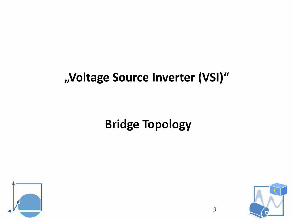
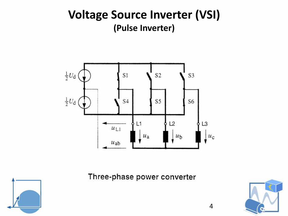
Voltage Source Inverter (VSI) (Pulse Inverter)
+
-
+
-
+
-
motor
U0
4
Voltage Source Inverter (VSI) (Pulse Inverter)
5
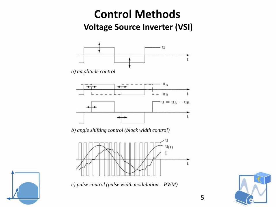
Control MethodsVoltage Source Inverter (VSI)
a) amplitude control
b) angle shifting control (block width control)
c) pulse control (pulse width modulation – PWM)
6
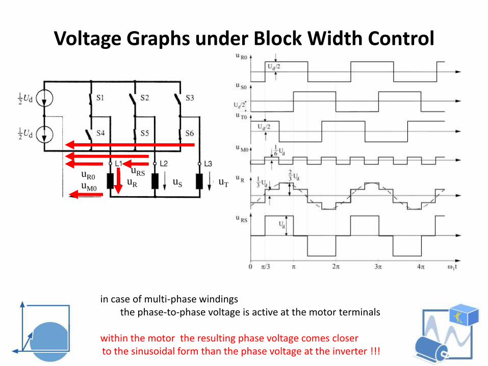
Voltage Graphs under Block Width Control
in case of multi-phase windingsthe phase-to-phase voltage is active at the motor terminals
within the motor the resulting phase voltage comes closer to the sinusoidal form than the phase voltage at the inverter !!!
uR uS uTuM0
uR0uRS
7
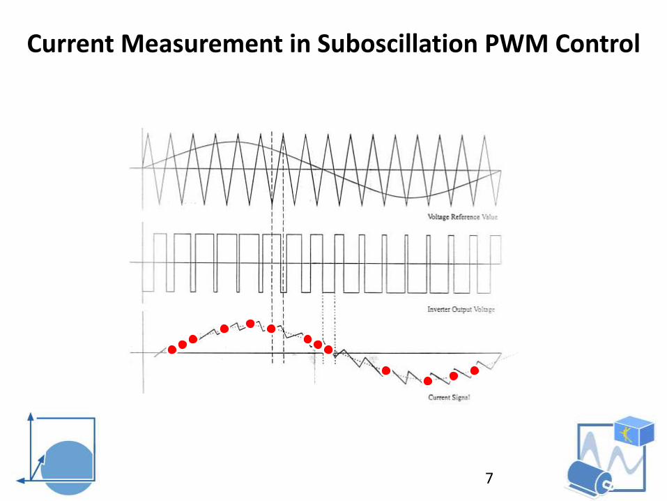
Current Measurement in Suboscillation PWM Control
8
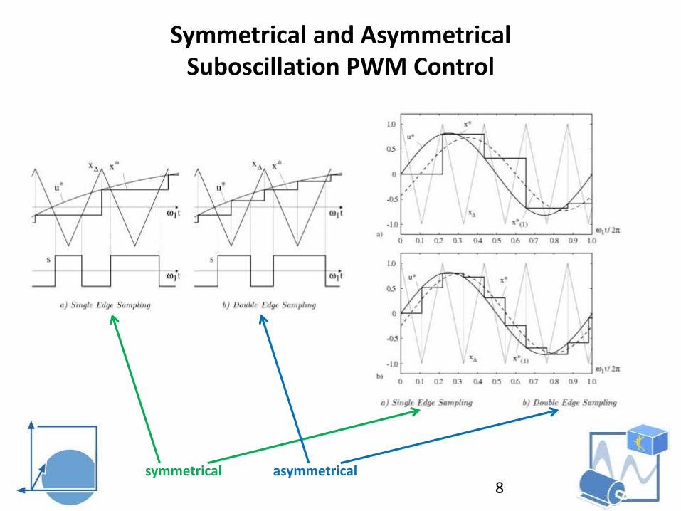
Symmetrical and AsymmetricalSuboscillation PWM Control
symmetrical asymmetrical
9
10
11
12
13
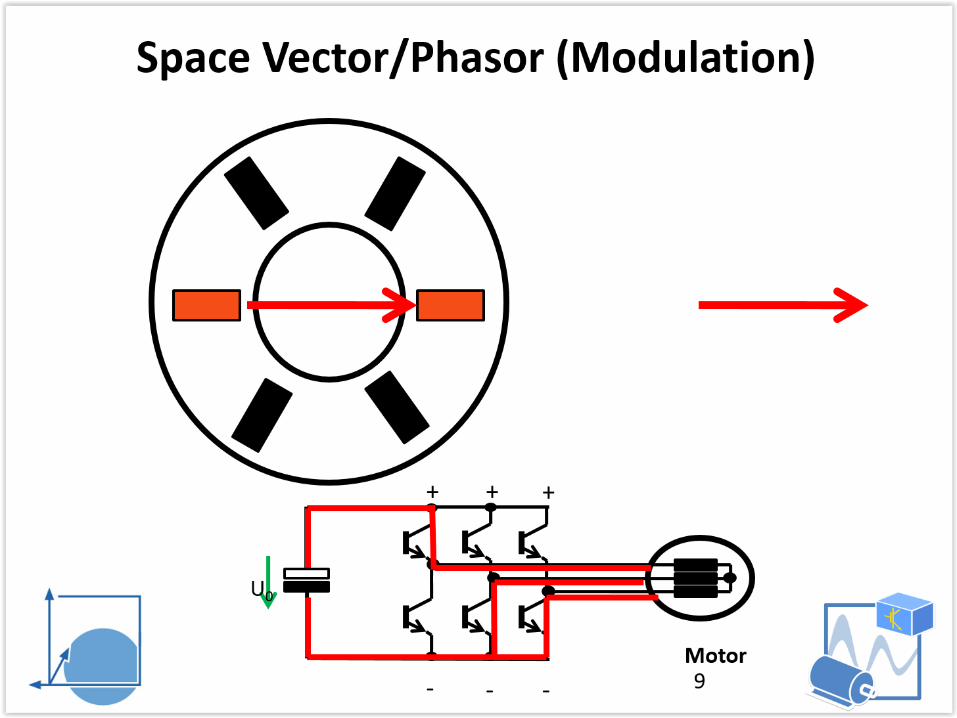
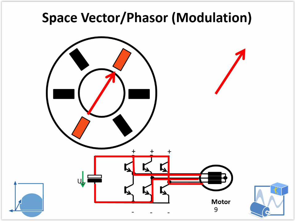
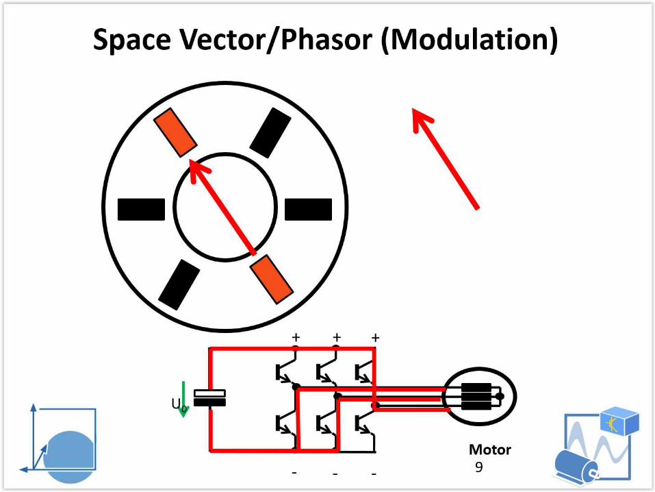
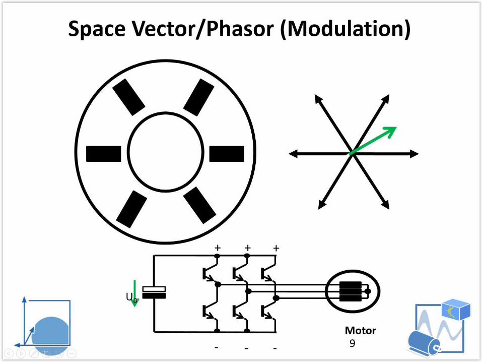
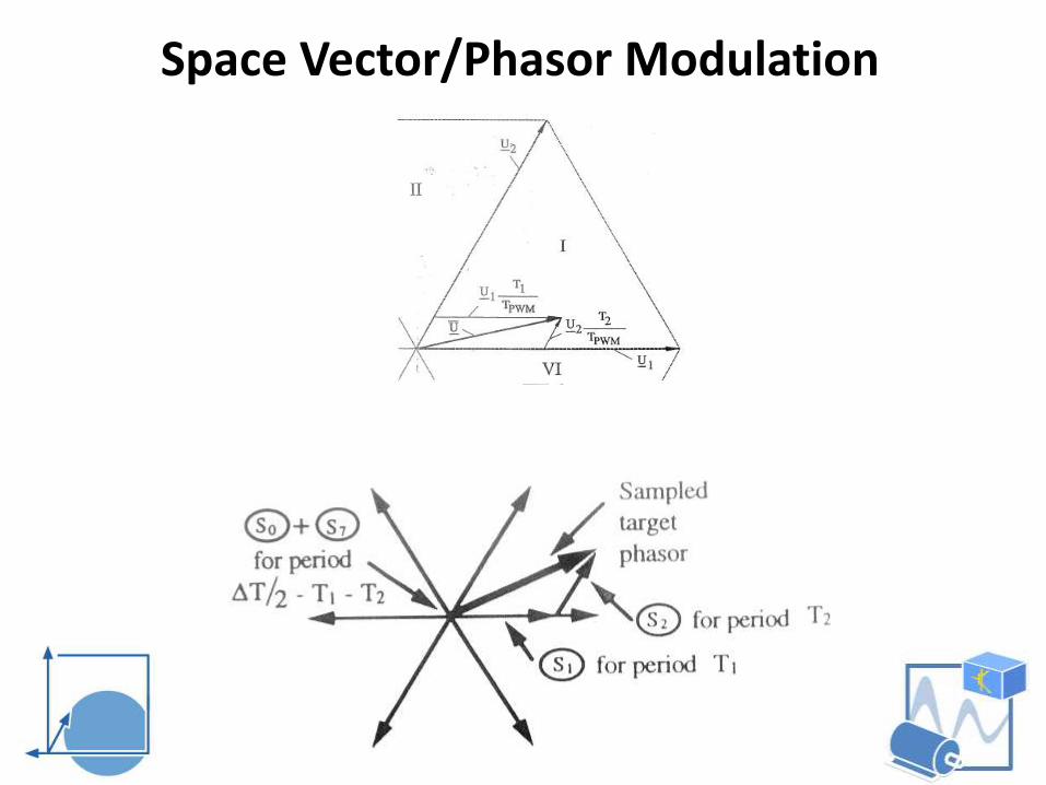
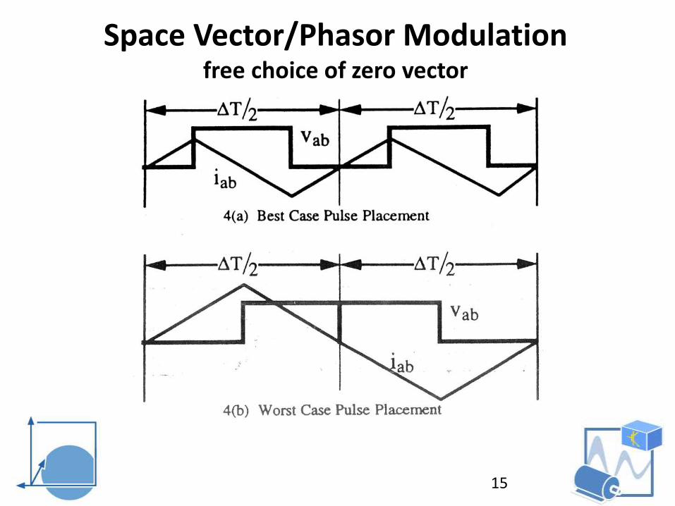
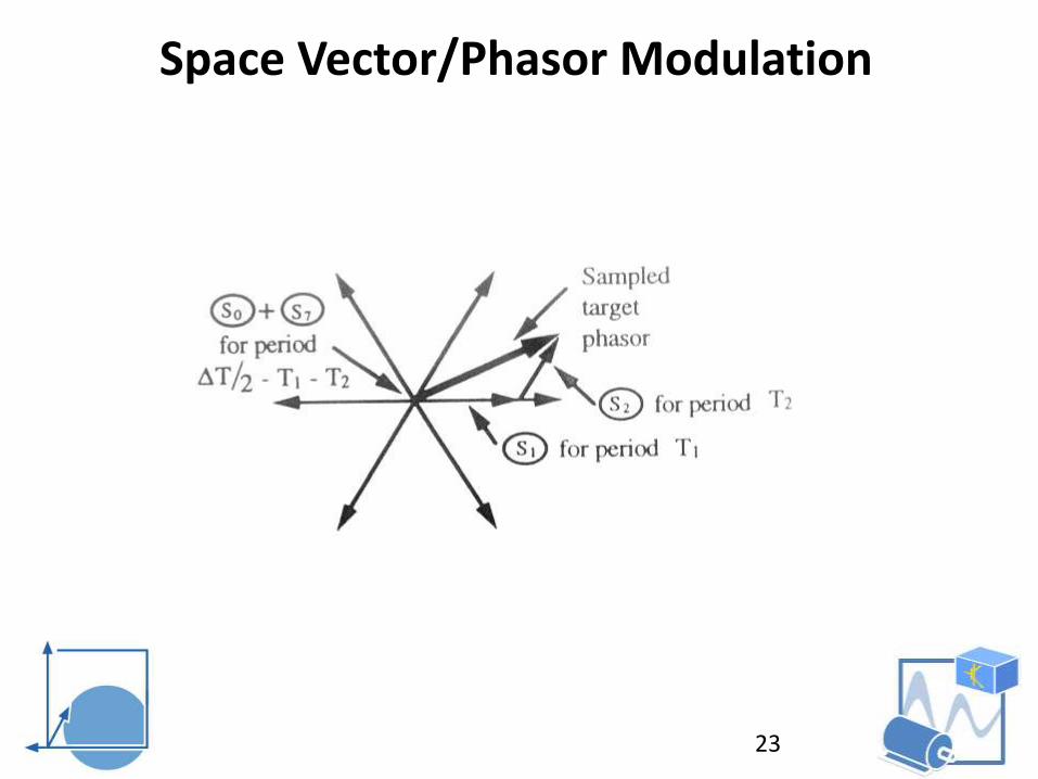
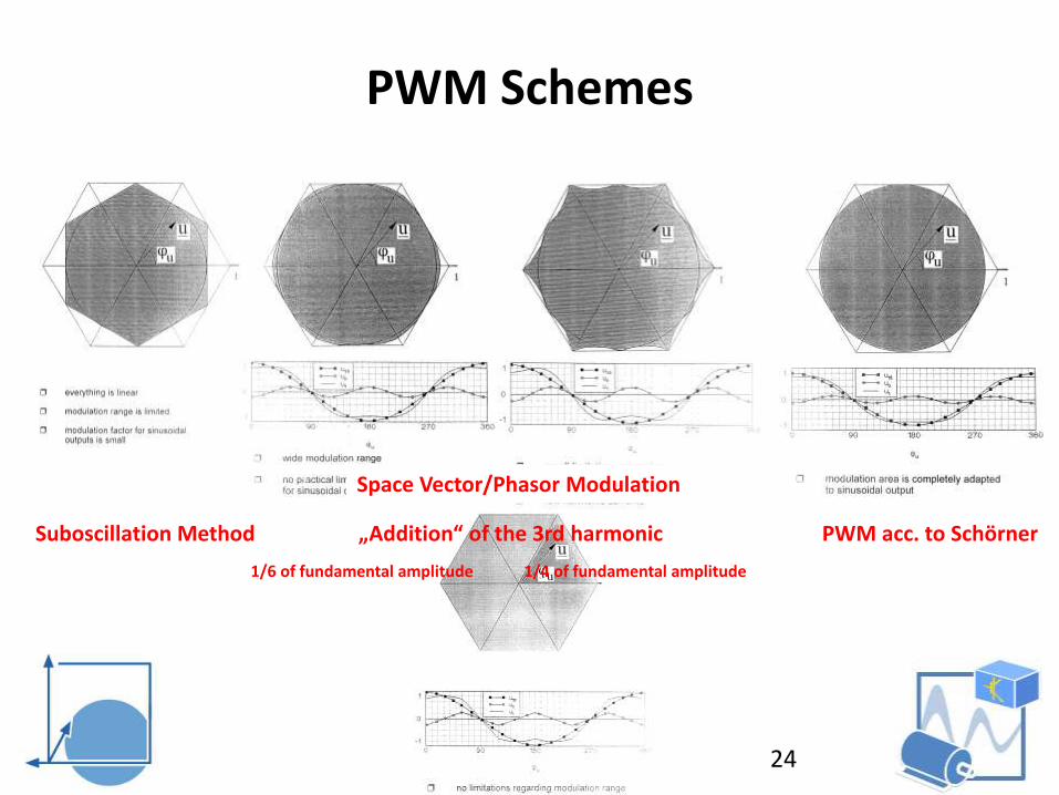
Space Vector/Phasor Modulation
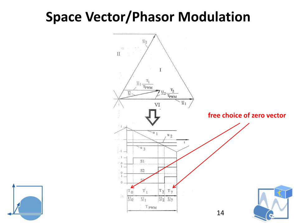
14
free choice of zero vector
Space Vector/Phasor Modulation
15
Space Vector/Phasor Modulationfree choice of zero vector
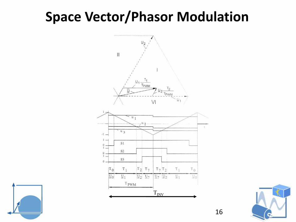
16
TINV
Space Vector/Phasor Modulation
17
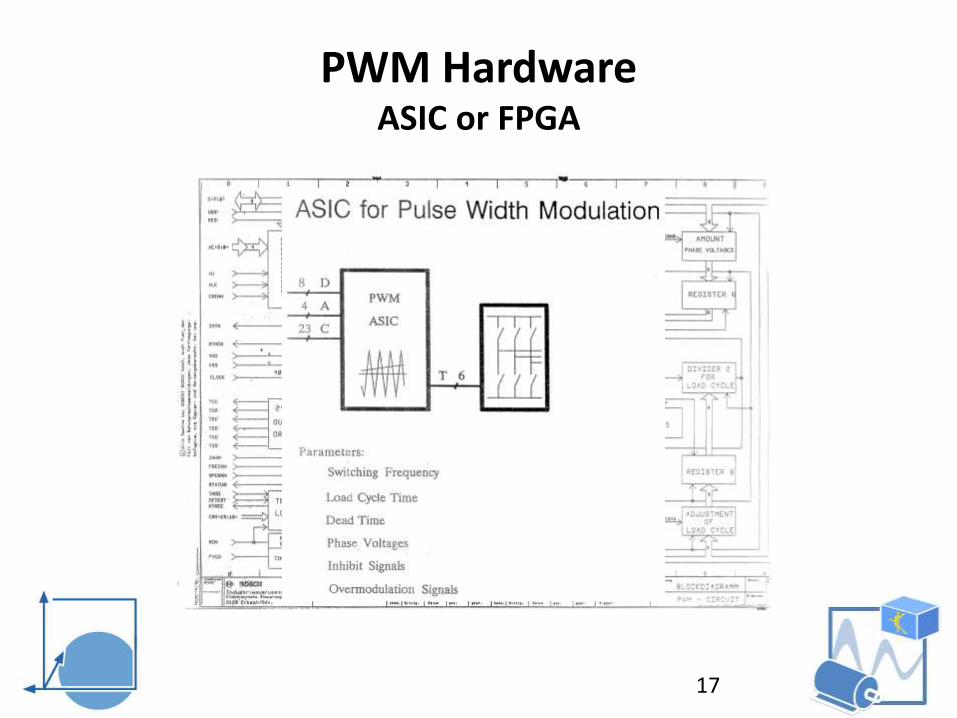
PWM HardwareASIC or FPGA
18
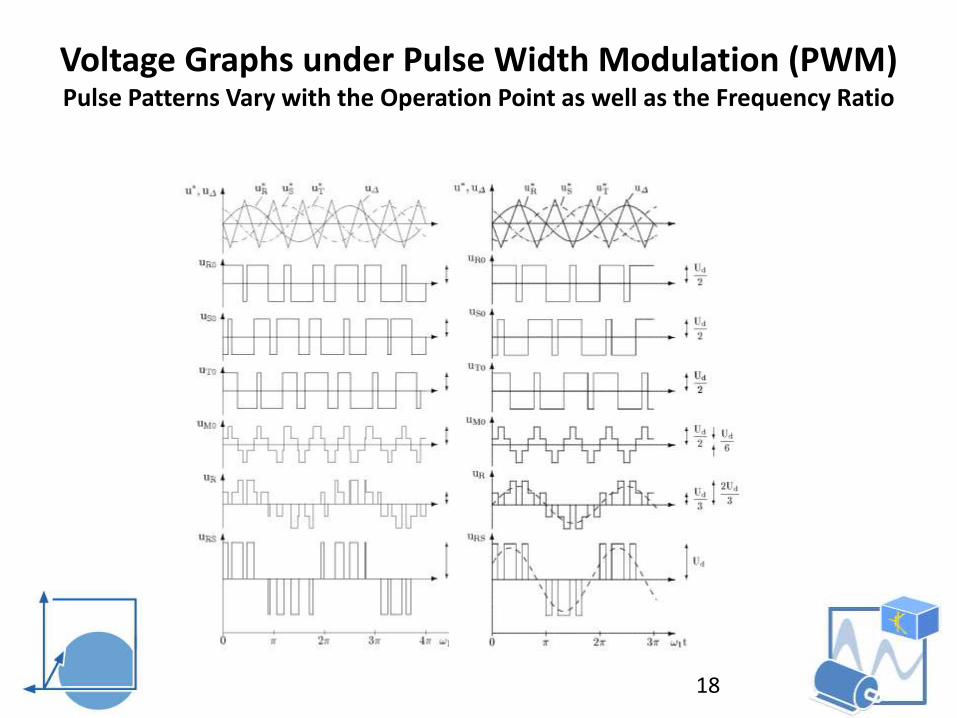
Voltage Graphs under Pulse Width Modulation (PWM)Pulse Patterns Vary with the Operation Point as well as the Frequency Ratio
19
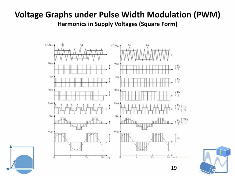
Voltage Graphs under Pulse Width Modulation (PWM)Harmonics in Supply Voltages (Square Form)
20
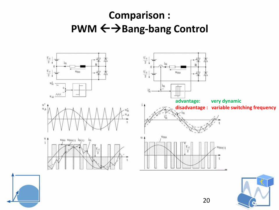
Comparison :PWM Bang-bang Control
advantage: very dynamicdisadvantage : variable switching frequency
21
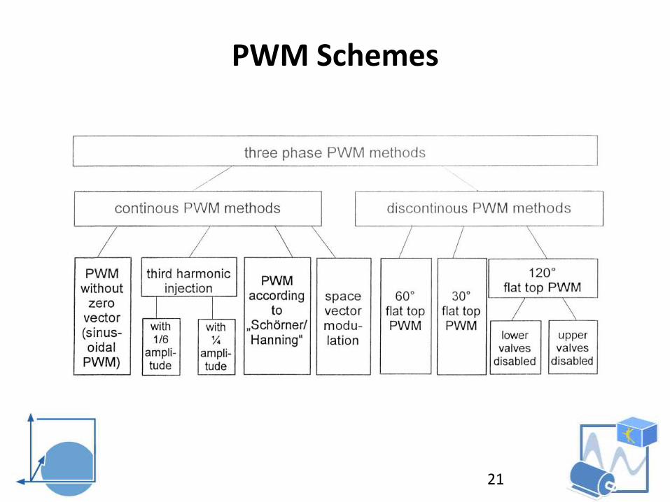
PWM Schemes
22
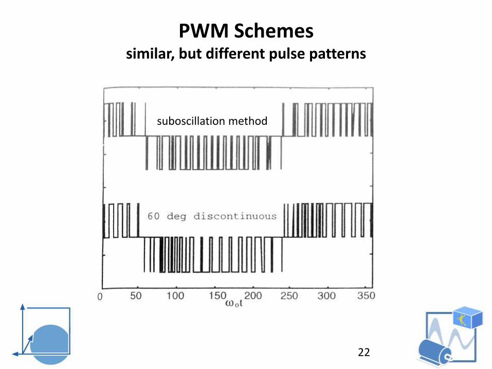
PWM Schemessimilar, but different pulse patterns
Unterschwingungsverfahrensuboscillation method
23
Space Vector/Phasor Modulation
24
Suboscillation Method „Addition“ of the 3rd harmonic
1/6 of fundamental amplitude 1/4 of fundamental amplitude
PWM acc. to Schörner
Space Vector/Phasor Modulation
PWM Schemes
25
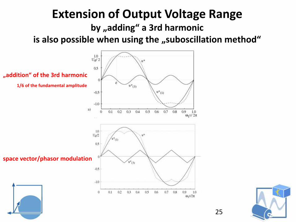
Extension of Output Voltage Rangeby „adding“ a 3rd harmonic
is also possible when using the „suboscillation method“
„addition“ of the 3rd harmonic
1/6 of the fundamental amplitude
space vector/phasor modulation
26
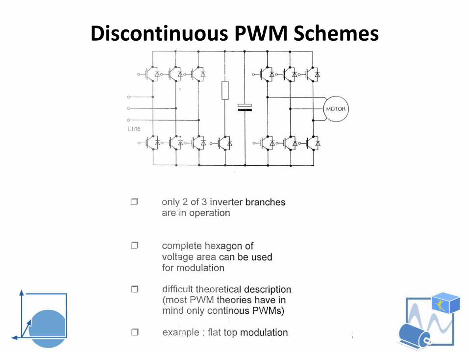
Discontinuous PWM Schemes
DC Link Capacitor Design
Prof. Dr.‐Ing. Ralph Kennel
Technische Universität München
Arcisstraße 21
80333 München
28
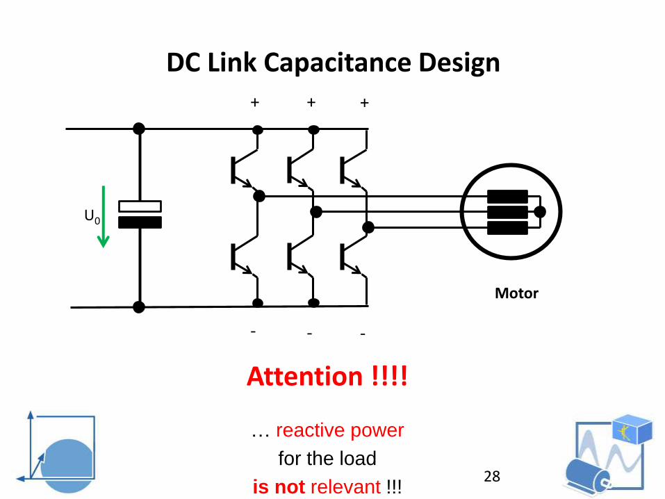
DC Link Capacitance Design
Attention !!!!
… reactive power
for the load
is not relevant !!!
+
-
+
-
+
-
Motor
U0
29
30
31
32
33
34
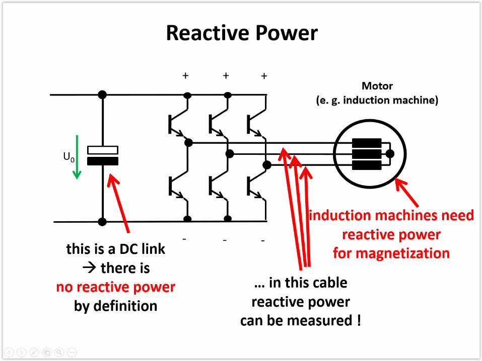
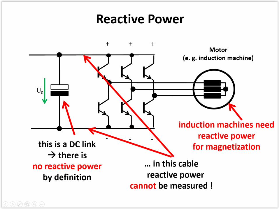
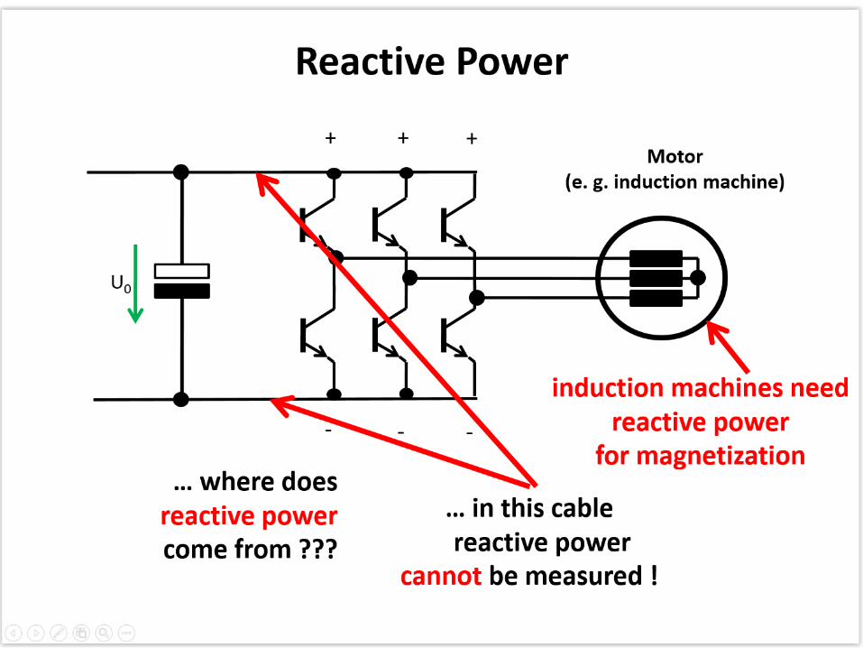
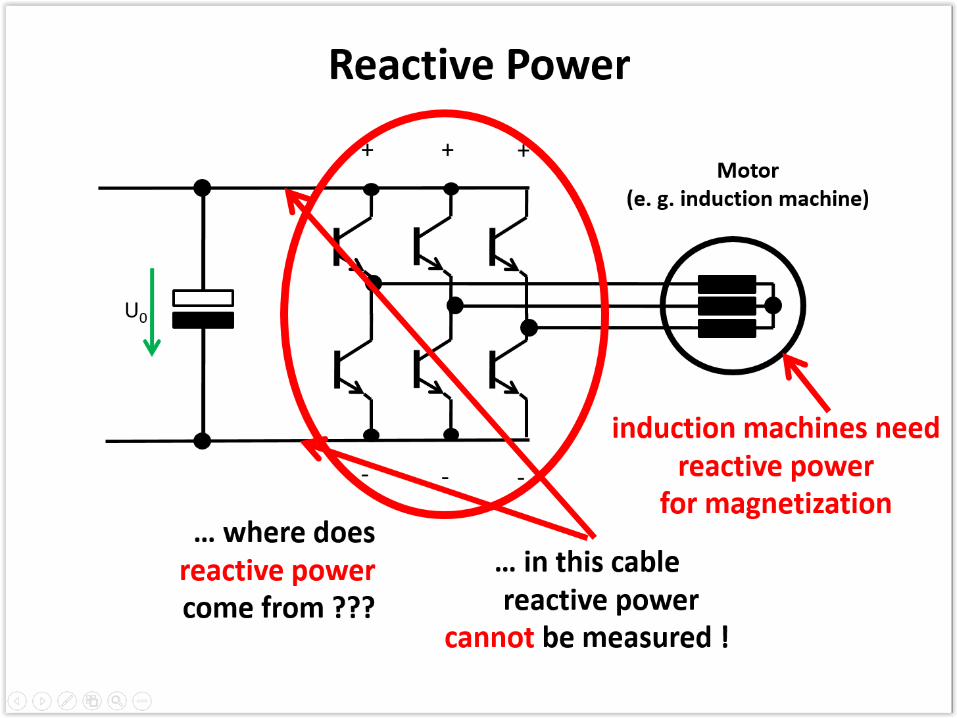
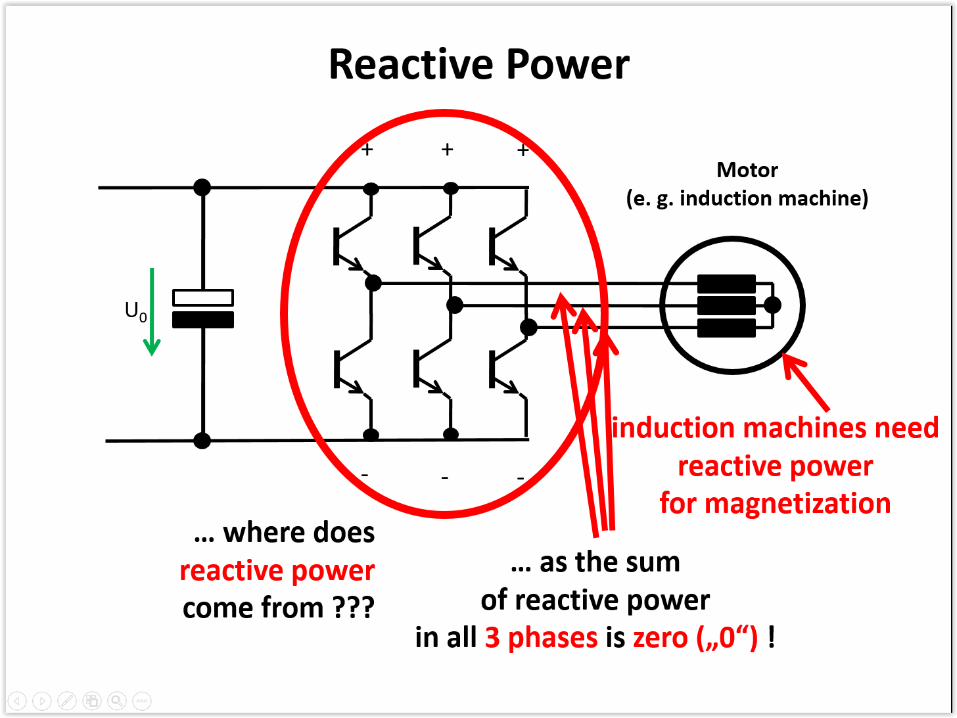
Reactive Power
+
-
+
-
+
-
Motor(e. g. induction machine)
U0
induction machines needreactive power
for magnetization… where does
reactive powercome from ???
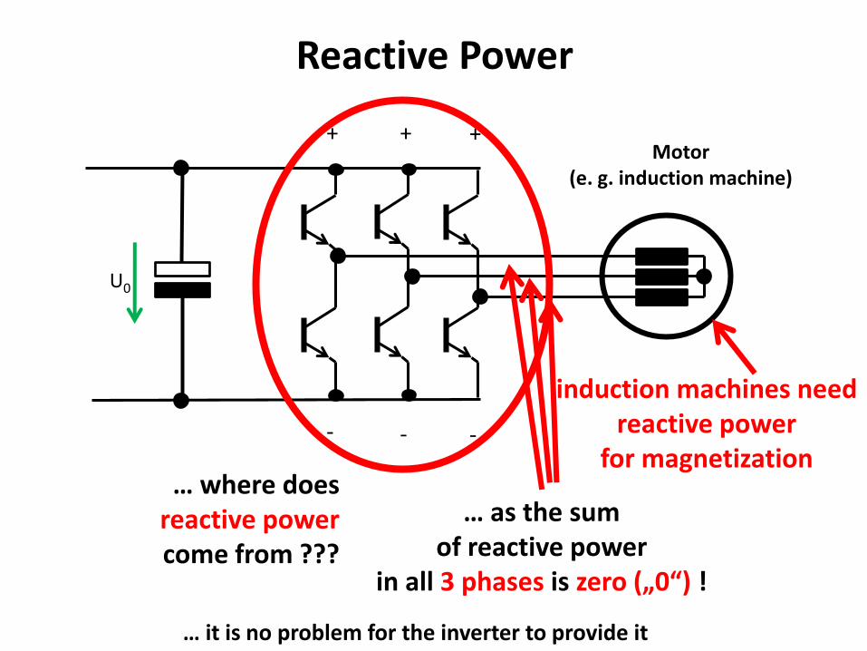
… it is no problem for the inverter to provide it
… as the sumof reactive power
in all 3 phases is zero („0“) !
35
Reactive Power
+
-
+
-
+
-
Motor(e. g. induction machine)
U0
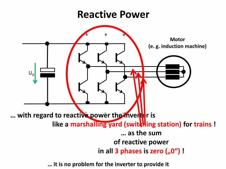
… it is no problem for the inverter to provide it
… as the sumof reactive power
in all 3 phases is zero („0“) !
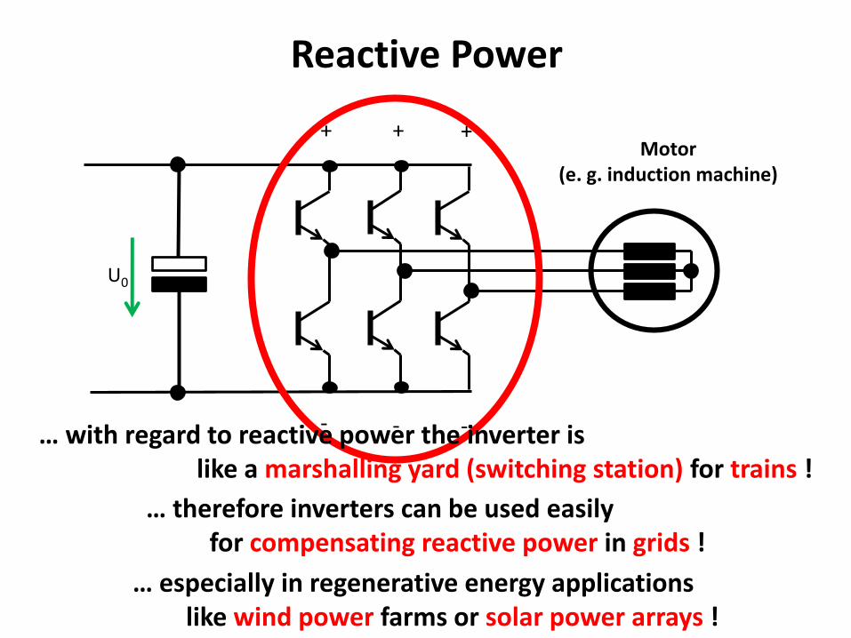
… with regard to reactive power the inverter is like a marshalling yard (switching station) for trains !
36
Reactive Power
+
-
+
-
+
-
Motor(e. g. induction machine)
U0
… with regard to reactive power the inverter is like a marshalling yard (switching station) for trains !
… therefore inverters can be used easily for compensating reactive power in grids !
… especially in regenerative energy applicationslike wind power farms or solar power arrays !
37
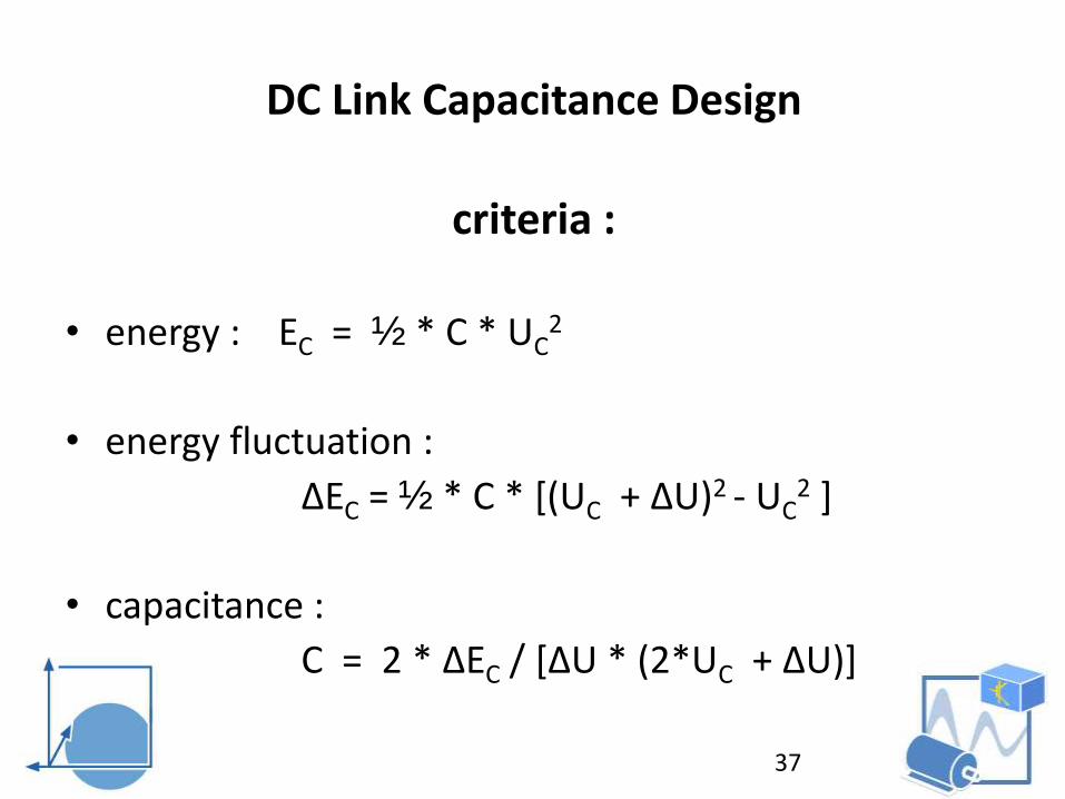
criteria :
• energy : EC = ½ * C * UC2
• energy fluctuation :
∆EC = ½ * C * [(UC + ∆U)2 - UC2 ]
• capacitance :
C = 2 * ∆EC / [∆U * (2*UC + ∆U)]
DC Link Capacitance Design
38
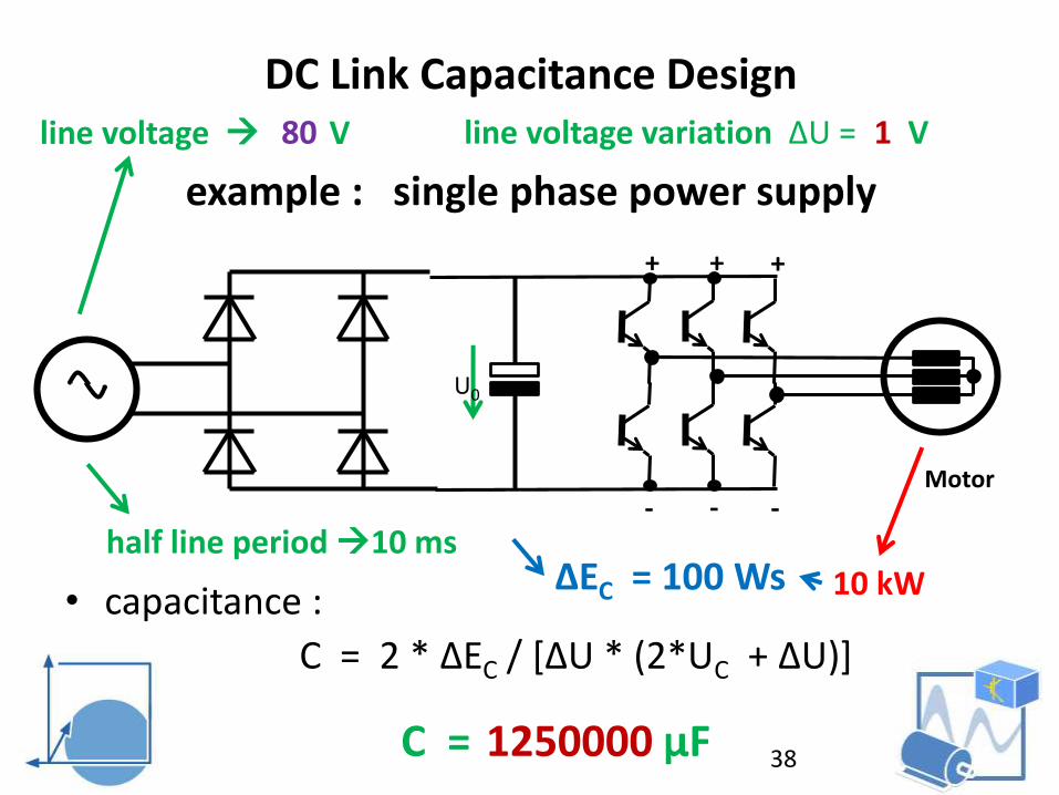
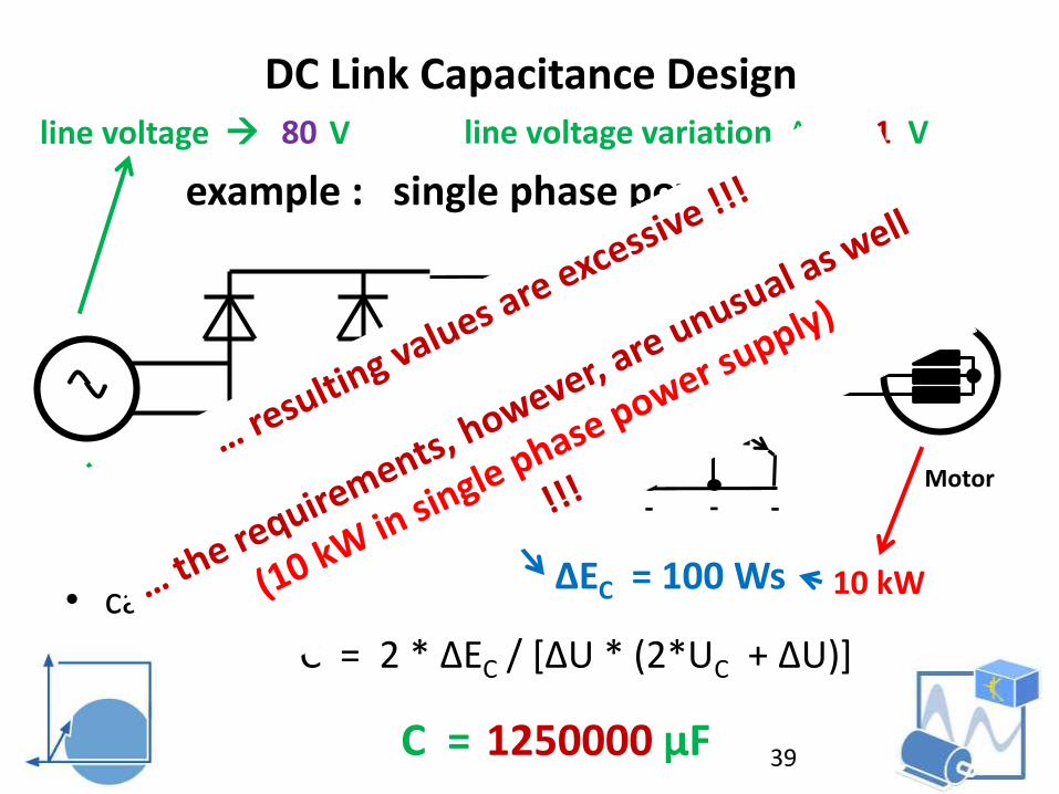
example : single phase power supply
• capacitance :
C = 2 * ∆EC / [∆U * (2*UC + ∆U)]
+
-
+
-
+
-Motor
U0
C = 1800 µF
10 kWhalf line period10 ms
∆EC = 100 Ws
line voltage 550 V line voltage variation ∆U = 10 V80
11800
1
1250000
DC Link Capacitance Design
39
example : single phase power supply
• capacitance :
C = 2 * ∆EC / [∆U * (2*UC + ∆U)]
+
-
+
-
+
-Motor
U0
C = 1800 µF
10 kWhalf line period10 ms
∆EC = 100 Ws
line voltage 550 V line voltage variation ∆U = 10 V80
11800
1
1250000
DC Link Capacitance Design
40
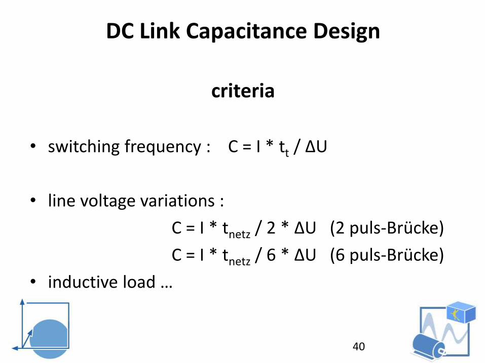
DC Link Capacitance Design
criteria
• switching frequency : C = I * tt / ∆U
• line voltage variations :
C = I * tnetz / 2 * ∆U (2 puls-Brücke)
C = I * tnetz / 6 * ∆U (6 puls-Brücke)
• inductive load …
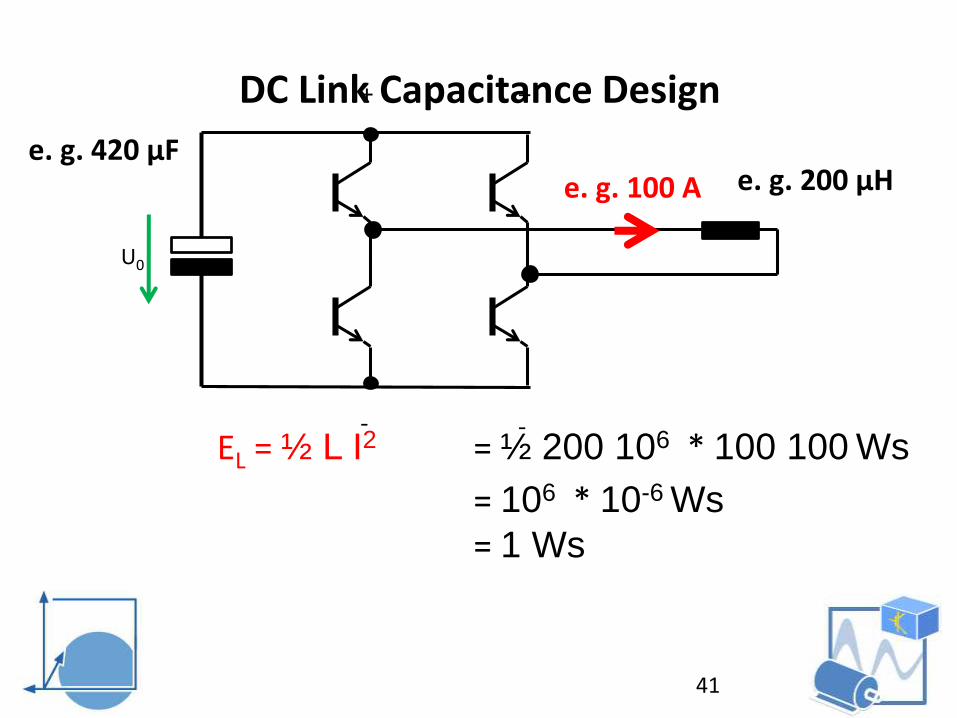
41
EL = ½ L I2
+
-
+
-
U0
e. g. 100 A e. g. 200 µH e. g. 420 µF
= ½ 200 106 * 100 100 Ws
= 106 * 10-6 Ws
= 1 Ws
DC Link Capacitance Design
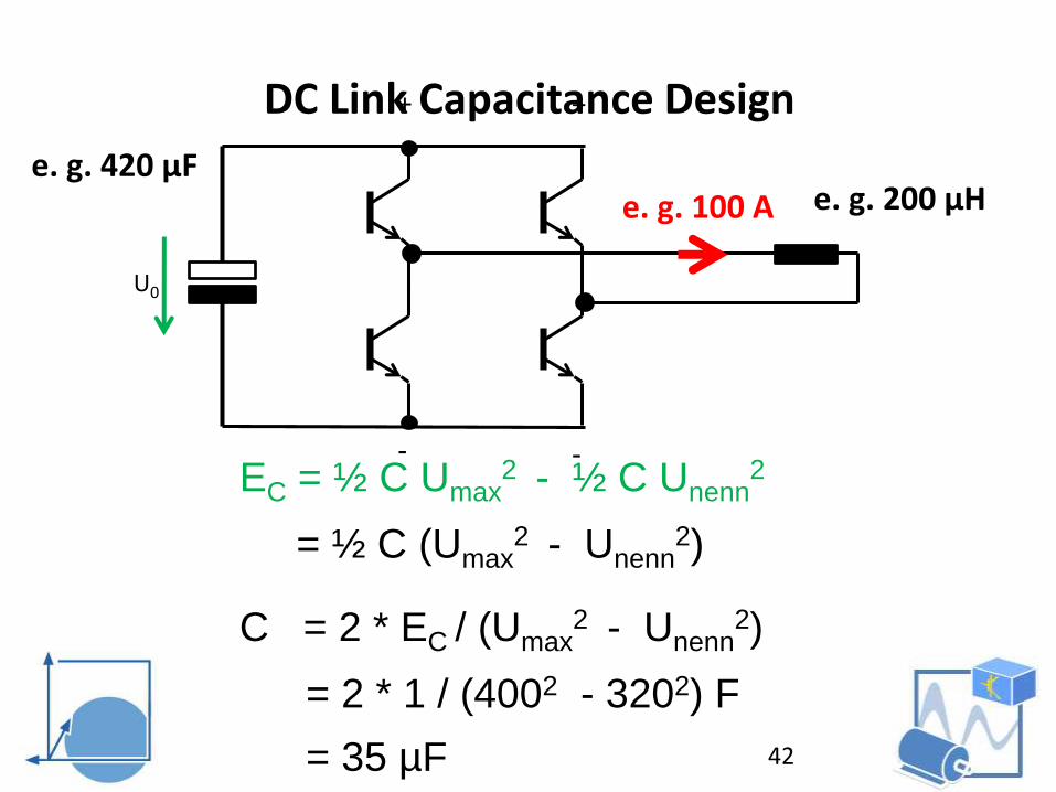
42
EC = ½ C Umax2 - ½ C Unenn
2
+
-
+
-
U0
e. g. 100 A e. g. 200 µH e. g. 420 µF
C = 2 * EC / (Umax2 - Unenn
2)
= 2 * 1 / (4002 - 3202) F
= 35 µF
= ½ C (Umax2 - Unenn
2)
DC Link Capacitance Design
43
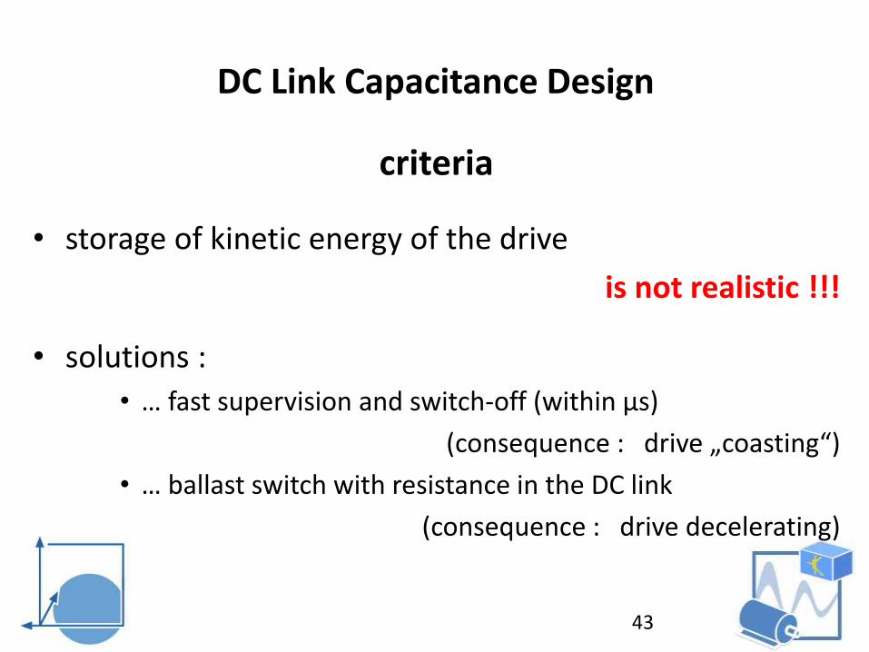
criteria
• storage of kinetic energy of the drive
is not realistic !!!
• solutions :
• … fast supervision and switch-off (within µs)
(consequence : drive „coasting“)
• … ballast switch with resistance in the DC link
(consequence : drive decelerating)
DC Link Capacitance Design
44
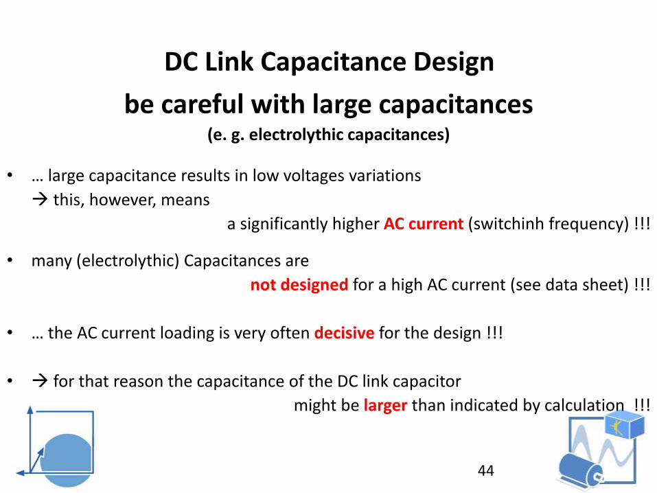
be careful with large capacitances(e. g. electrolythic capacitances)
• … large capacitance results in low voltages variations
this, however, means
a significantly higher AC current (switchinh frequency) !!!
• many (electrolythic) Capacitances are
not designed for a high AC current (see data sheet) !!!
• … the AC current loading is very often decisive for the design !!!
• for that reason the capacitance of the DC link capacitor
might be larger than indicated by calculation !!!
DC Link Capacitance Design
45
„Voltage Source Inverter (VSI)“
TopologiesSpecific for Automotive Applications
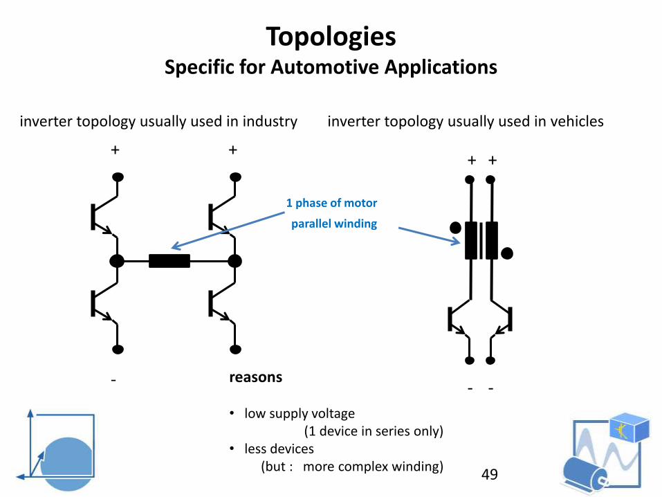
46
47
48
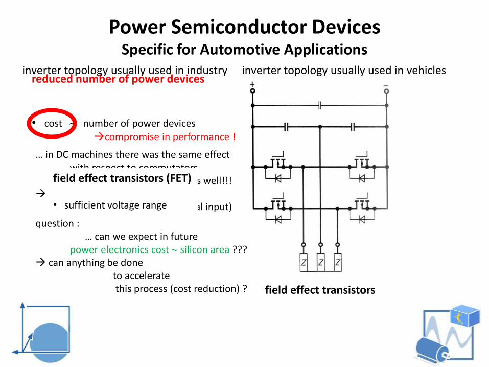
reduced number of power devices
• cost number of power devicescompromise in performance !
… in DC machines there was the same effectwith respect to commutators
in earlier times as well!!! today : commutator cost
commutator size (material input)
field effect transistors (FET)
• sufficient voltage range• high switching frequency
inverter topology usually used in vehiclesinverter topology usually used in industry
Power Semiconductor DevicesSpecific for Automotive Applications
bipolar transistors field effect transistors
question :… can we expect in future
power electronics cost silicon area ??? can anything be done
to acceleratethis process (cost reduction) ?
49
TopologiesSpecific for Automotive Applications
+
-
+
-
inverter topology usually used in industry
+ +
--
inverter topology usually used in vehicles
reasons
• low supply voltage(1 device in series only)
• less devices(but : more complex winding)
1 phase of motor
parallel winding