F R A U N H O F E R I N S T I T U T E F O R I N T E G R AT E D S Y S T E M S A N D D E V I C E T E C H N O L O G Y I I S B
CONTACT
Fraunhofer Institute for Integrated Systems and Device Technology IISB
Schottkystrasse 10
91058 Erlangen, Germany
www.iisb.fraunhofer.de
Dr. Jochen Friedrich
Phone: +49 (0) 9131 761-270
Fax: +49 (0) 9131 761-280
Fraunhofer Technology Center for Semiconductor Materials THM
Am St. Niclas Schacht 13
09599 Freiberg/Sachsen
www.thm.fraunhofer.de
Dr. Jochen Friedrich
Phone: +49 (0) 3731 2033-102
Fax: +49 (0) 3731 2033-199
© F r a u n h o f e r I I S B | w w w . i i s b . f r a u n h o f e r . d e
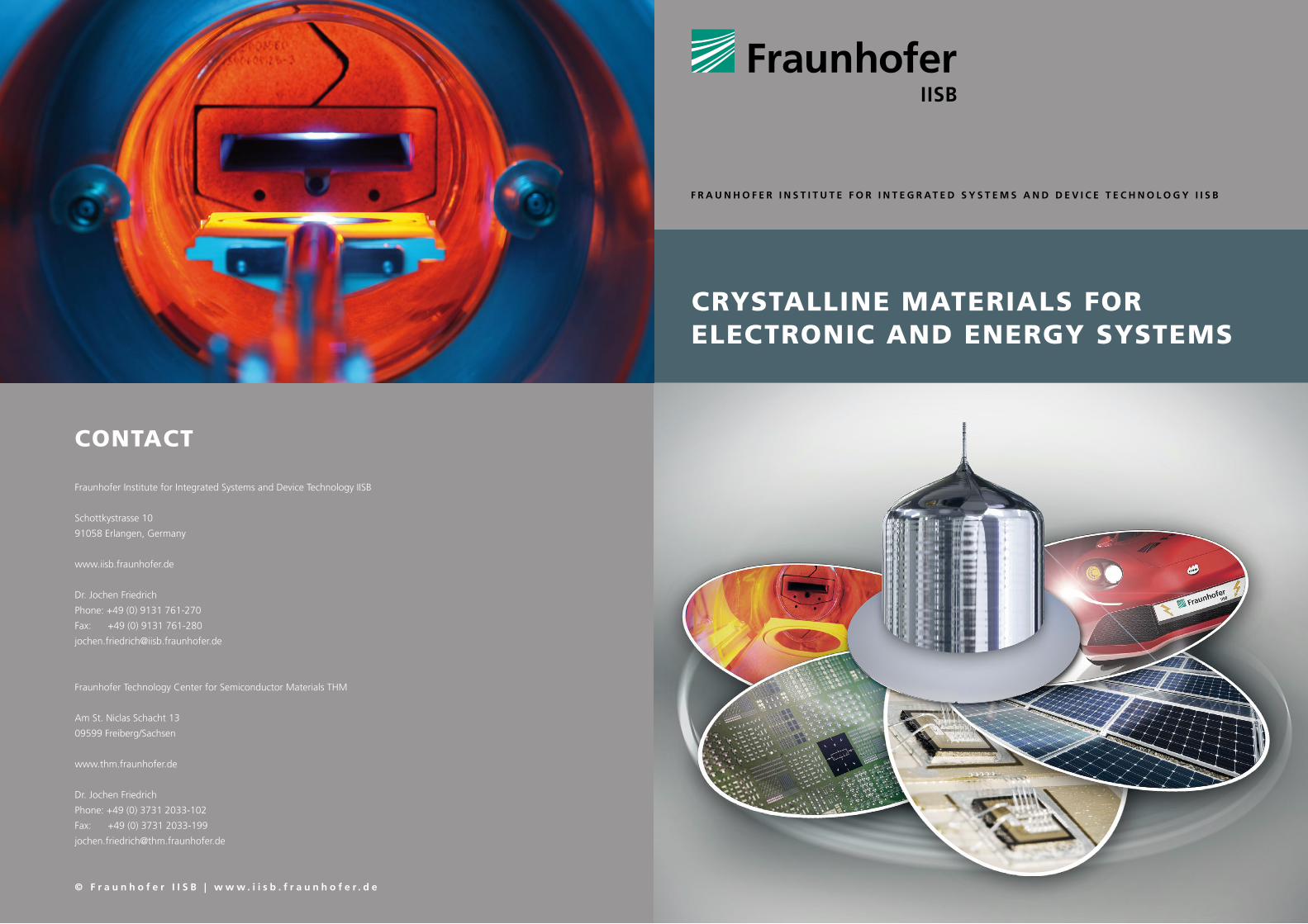
CRYSTALLINE MATERIALS FOR ELECTRONIC AND ENERGY SYSTEMS
Mission
Our mission is to deliver outstanding scientific-technological solutions in the field of crystalline
materials and their production in such a way that the commercialization of these materials will
be pushed forward and the production of new applications from these materials will become
possible. The especially address markets for semiconductors, oxides, halides and other dielectric
materials for electronic, energy and optical systems. We support material, device, and equipment
manufacturers and their suppliers in the areas of crystal growth, epitaxy, thin film deposition, and
synthesis of nanometer-sized powders.
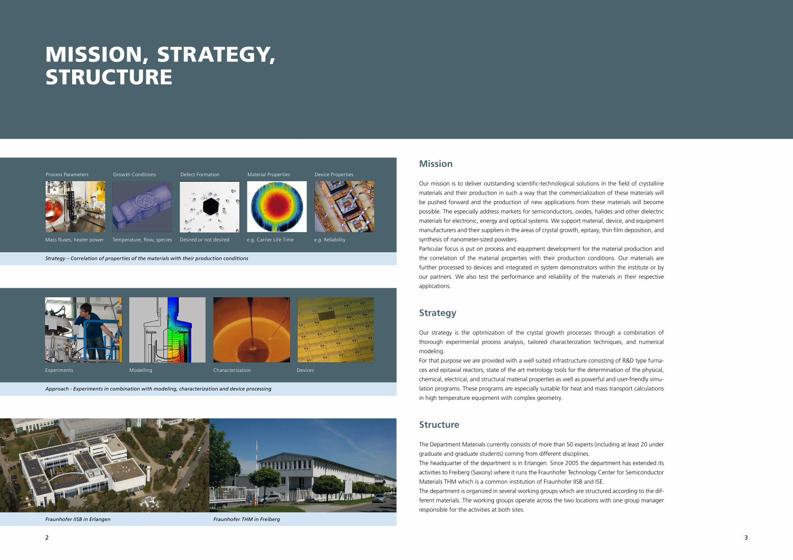
Particular focus is put on process and equipment development for the material production and
the correlation of the material properties with their production conditions. Our materials are
further processed to devices and integrated in system demonstrators within the institute or by
our partners. We also test the performance and reliability of the materials in their respective
applications.
Strategy
Our strategy is the optimization of the crystal growth processes through a combination of
thorough experimental process analysis, tailored characterization techniques, and numerical
modeling.
For that purpose we are provided with a well suited infrastructure consisting of R&D type furna-
ces and epitaxial reactors, state of the art metrology tools for the determination of the physical,
chemical, electrical, and structural material properties as well as powerful and user-friendly simu-
lation programs. These programs are especially suitable for heat and mass transport calculations
in high temperature equipment with complex geometry.
Structure
The Department Materials currently consists of more than 50 experts (including at least 20 under
graduate and graduate students) coming from different disciplines.
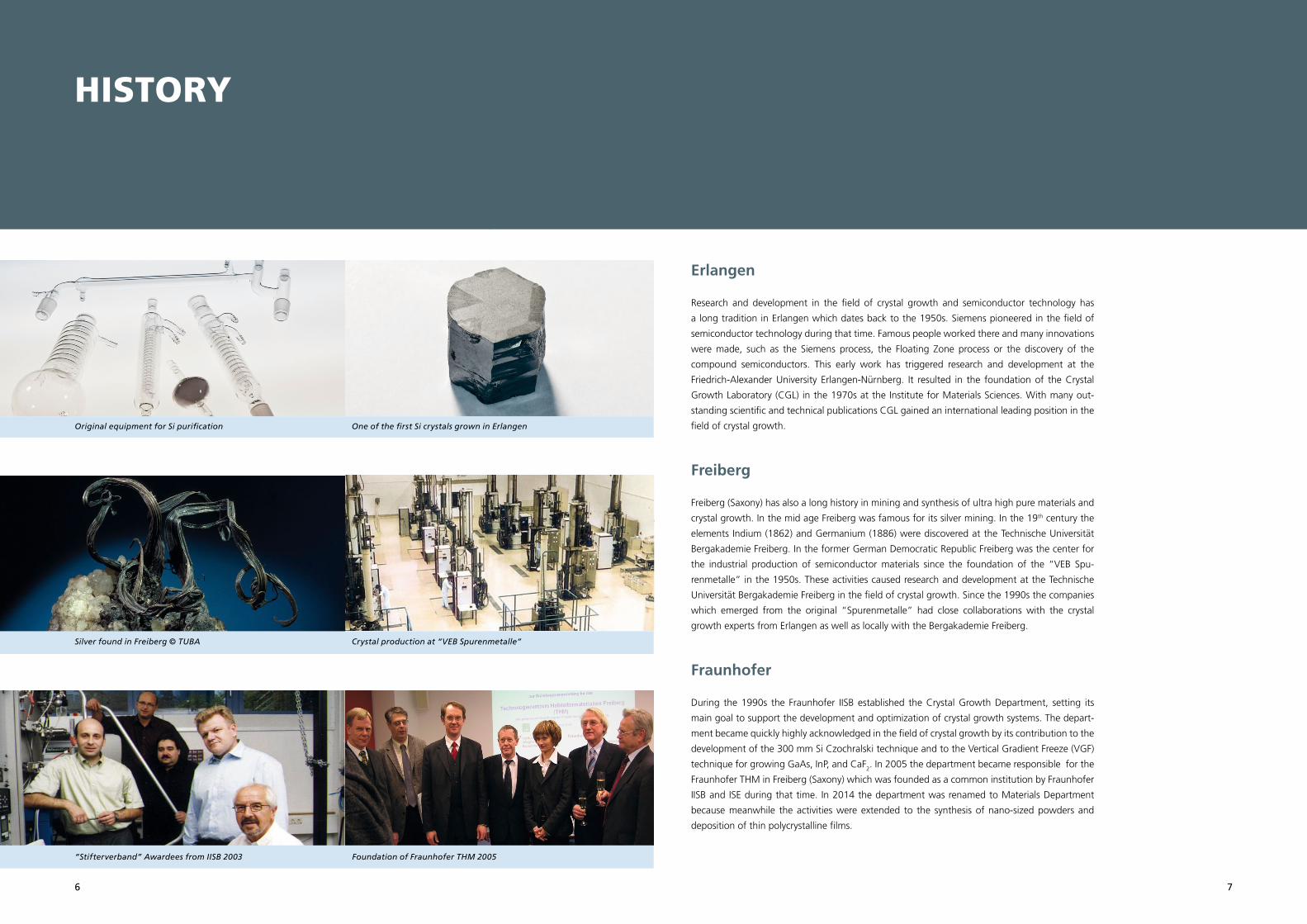
The headquarter of the department is in Erlangen. Since 2005 the department has extended its
activities to Freiberg (Saxony) where it runs the Fraunhofer Technology Center for Semiconductor
Materials THM which is a common institution of Fraunhofer IISB and ISE.
The department is organized in several working groups which are structured according to the dif-
ferent materials. The working groups operate across the two locations with one group manager
responsible for the activities at both sites.
MISSION, STRATEGY, STRUCTURE
Fraunhofer IISB in Erlangen Fraunhofer THM in Freiberg
Strategy – Correlation of properties of the materials with their production conditions
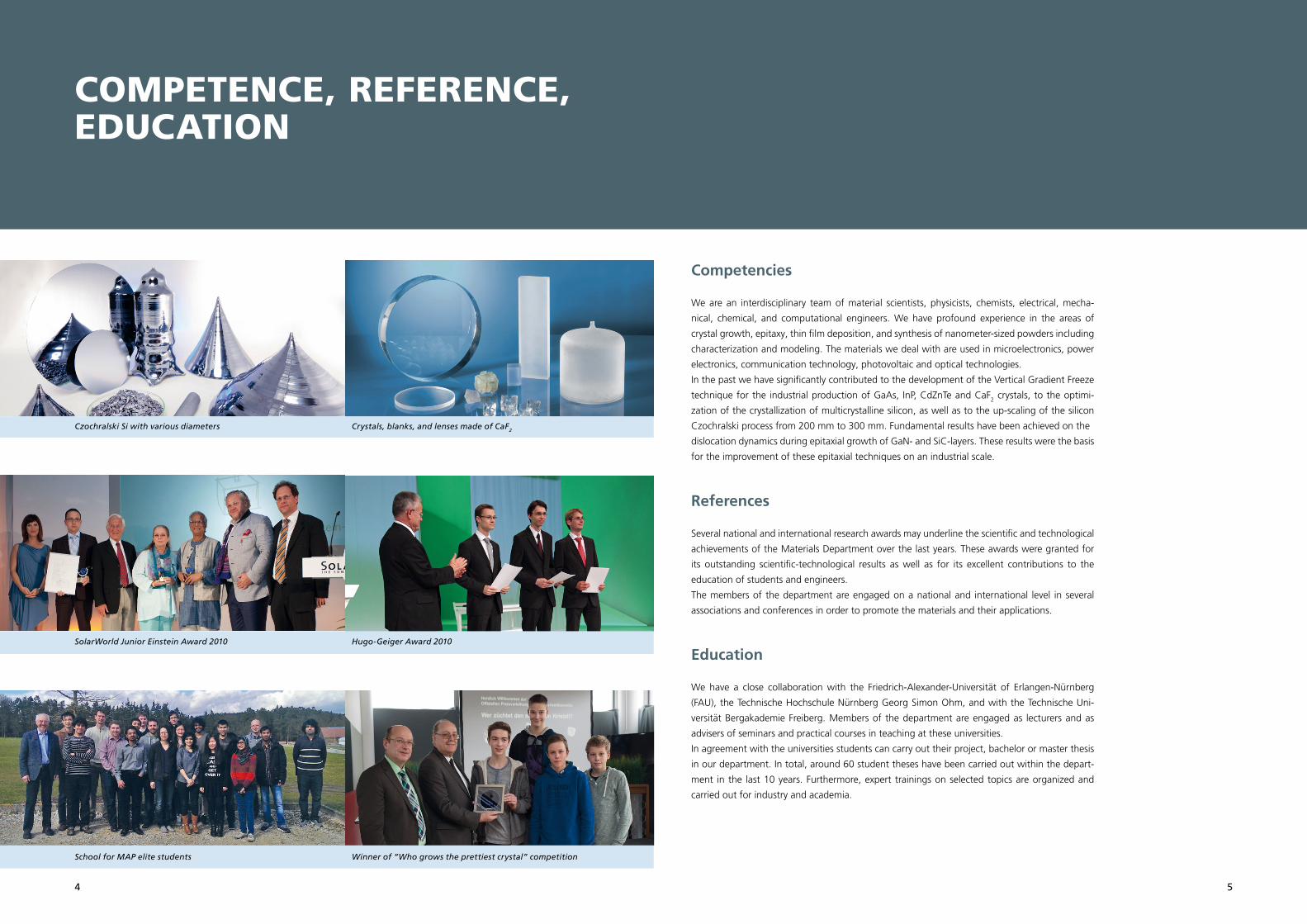
Approach - Experiments in combination with modeling, characterization and device processing
Experiments Modelling Characterization Devices
Process Parameters
Mass fluxes, heater power
Growth Conditions
Temperature, flow, species
Defect Formation
Desired or not desired
Material Properties
e.g. Carrier Life Time
Device Properties
e.g. Reliability
32
Competencies
We are an interdisciplinary team of material scientists, physicists, chemists, electrical, mecha-
nical, chemical, and computational engineers. We have profound experience in the areas of
crystal growth, epitaxy, thin film deposition, and synthesis of nanometer-sized powders including
characterization and modeling. The materials we deal with are used in microelectronics, power
electronics, communication technology, photovoltaic and optical technologies.
In the past we have significantly contributed to the development of the Vertical Gradient Freeze
technique for the industrial production of GaAs, InP, CdZnTe and CaF2 crystals, to the optimi-
zation of the crystallization of multicrystalline silicon, as well as to the up-scaling of the silicon
Czochralski process from 200 mm to 300 mm. Fundamental results have been achieved on the
dislocation dynamics during epitaxial growth of GaN- and SiC-layers. These results were the basis
for the improvement of these epitaxial techniques on an industrial scale.
References
Several national and international research awards may underline the scientific and technological
achievements of the Materials Department over the last years. These awards were granted for
its outstanding scientific-technological results as well as for its excellent contributions to the
education of students and engineers.
The members of the department are engaged on a national and international level in several
associations and conferences in order to promote the materials and their applications.
Education
We have a close collaboration with the Friedrich-Alexander-Universität of Erlangen-Nürnberg
(FAU), the Technische Hochschule Nürnberg Georg Simon Ohm, and with the Technische Uni-
versität Bergakademie Freiberg. Members of the department are engaged as lecturers and as
advisers of seminars and practical courses in teaching at these universities.
In agreement with the universities students can carry out their project, bachelor or master thesis
in our department. In total, around 60 student theses have been carried out within the depart-
ment in the last 10 years. Furthermore, expert trainings on selected topics are organized and
carried out for industry and academia.
COMPETENCE, REFERENCE, EDUCATION
Czochralski Si with various diameters
SolarWorld Junior Einstein Award 2010
School for MAP elite students Winner of “Who grows the prettiest crystal” competition
Hugo-Geiger Award 2010
Crystals, blanks, and lenses made of CaF2
54
HISTORY
Erlangen
Research and development in the field of crystal growth and semiconductor technology has
a long tradition in Erlangen which dates back to the 1950s. Siemens pioneered in the field of
semiconductor technology during that time. Famous people worked there and many innovations
were made, such as the Siemens process, the Floating Zone process or the discovery of the
compound semiconductors. This early work has triggered research and development at the
Friedrich-Alexander University Erlangen-Nürnberg. It resulted in the foundation of the Crystal
Growth Laboratory (CGL) in the 1970s at the Institute for Materials Sciences. With many out-
standing scientific and technical publications CGL gained an international leading position in the
field of crystal growth.
Freiberg
Freiberg (Saxony) has also a long history in mining and synthesis of ultra high pure materials and
crystal growth. In the mid age Freiberg was famous for its silver mining. In the 19th century the
elements Indium (1862) and Germanium (1886) were discovered at the Technische Universität
Bergakademie Freiberg. In the former German Democratic Republic Freiberg was the center for
the industrial production of semiconductor materials since the foundation of the “VEB Spu-
renmetalle” in the 1950s. These activities caused research and development at the Technische
Universität Bergakademie Freiberg in the field of crystal growth. Since the 1990s the companies
which emerged from the original “Spurenmetalle” had close collaborations with the crystal
growth experts from Erlangen as well as locally with the Bergakademie Freiberg.
Fraunhofer
During the 1990s the Fraunhofer IISB established the Crystal Growth Department, setting its
main goal to support the development and optimization of crystal growth systems. The depart-
ment became quickly highly acknowledged in the field of crystal growth by its contribution to the
development of the 300 mm Si Czochralski technique and to the Vertical Gradient Freeze (VGF)
technique for growing GaAs, InP, and CaF2. In 2005 the department became responsible for the
Fraunhofer THM in Freiberg (Saxony) which was founded as a common institution by Fraunhofer
IISB and ISE during that time. In 2014 the department was renamed to Materials Department
because meanwhile the activities were extended to the synthesis of nano-sized powders and
deposition of thin polycrystalline films.
Original equipment for Si purification
Silver found in Freiberg © TUBA
“Stifterverband” Awardees from IISB 2003 Foundation of Fraunhofer THM 2005
Crystal production at “VEB Spurenmetalle”
One of the first Si crystals grown in Erlangen
76
SILICON
Services• We carry out our crystal growth experiments in special
R&D furnaces (1 kg up to 20 kg Si) and use equipment
at our partner‘s sites.
• We are equipped with a tailored sessile drop furnace to
investigate the melt crucible-coating interaction.
• We can perform coating and crucible tests.
• We are provided with a variety of structural, electrical,
Research TopicsSilicon is the most important material for electronic and photovoltaic applications.
In the fields of microelectronics and power electronics, we focus on heavily doped silicon crystals
grown by the Czochralski technique. The avoidance of dislocations during pulling, as well as de-
fect engineering in the heavily doped silicon in the as-grown state and during further processing,
are our main interest.
In the field of photovoltaics, we develop the directional solidification process as well as the
Czochralski method for producing silicon ingots with respect to lower production costs and
higher material quality. We concentrate on the reduction of defects which are limiting the mi-
nority carrier lifetime and subsequently the solar cell efficiency. Crystallographic lattice defects
like dislocation and grain boundaries, metallic impurities as well as light elements and resulting
foreign phase particles are in the focus of our research.
Furthermore, we are collaborating with suppliers in the area of silicon crystal growth along the
whole value chain. In this field, our research is based on testing and qualifying new furnace
materials, the development of innovative crucible and coating materials, on qualifying alternative
silicon feedstock, as well as on recycling of silicon sawing waste.
To reach our research goals we extensively use our structural, electrical, and chemical characte-
rization tools available at Fraunhofer IISB and Fraunhofer THM, as well as numerical simulation.
and chemical characterization tools.
• We develop and apply techniques to measure in-situ
temperatures, and the position of the solid-liquid inter-
face during crystal growth.
• We use numerical simulation to get an understanding of
the heat and mass transport processes, including how to
control the melt flow by magnetic fields.
Contact for further information:
Dr.-Ing. Christian Reimann
Phone: +49 9131 761-272
Tailored R&D G1 furnace
Sessile drop furnace for wetting analyses
Laue scanner for grain orientation analysis Striations in heavily doped Cz Si
EPD map of a mc Si sample
Typical grain structure of mc Si
98
SILICON CARBIDE
ServicesWe offer
• n- and p-type service epitaxy on 4H SiC wafers,
• processing of SiC prototype devices
(Schottky, MOS, diodes,…),
• in-depth characterization of substrates and epilayers
(e.g., by defect selective etching, X-ray topography,
photoluminescence imaging, lifetime measurements,…),
Research Topics4H-SiC is the ideal semiconductor for high-voltage and high-power electronic devices as well as
for sensor and detector applications in harsh environments. In close collaboration with substrate,
device, and equipment manufacturers we are developing epitaxy processes and characterization
methods for SiC tailored to specific device types. Our main goals in research and development
are to improve structural and electrical material quality, to reduce epitaxy cost, and to provide
special epitaxy for our customers.
We analyze structural defects in the substrates and their evolution into the epilayer during epi-
taxy and further device processing, and we investigate how the functionality and reliability of SiC
devices correlate with the crystal defects. We develop epitaxial processes for ultrathin and very
thick epilayers with high structural quality and high uniformity of the electrical properties.
Another research topic is to increase the minority carrier lifetime during epitaxy and device pro-
cessing. To reduce epitaxy cost we develop processes with increased growth rates while keeping
structural quality high.
The experimental work is complemented by numerical simulation of the fluid dynamics, heat
transfer, and species transport with chemical reactions during SiC bulk and epitaxial growth
processes.
• reliability investigations, and
• modeling of bulk SiC growth, epitaxy and annealing
processes.
Contact for further information:
Dr.-Ing. Patrick Berwian
Phone: +49 9131 761-135
Epitaxy on SiC substrates (100mm, 150mm)
PL imaging of SiC wafers and epilayers
Electrical characterization of SiC epilayers In house processed SiC MOSFETs
Lifetime map of SiC epilayer
Various dislocations in SiC visualized by DSE
1110
NITRIDES
ServicesWe offer to analyze bulk crystals, epilayers and devices be-
ginning at the macroscopic scale down to the atomic level:
• examination of defect etched samples using optical
microscopy,
• several analytical methods such as elemental analysis
using a special energy dispersive X-ray detector,
• a miniaturized four point probe set-up inside a scanning
Research TopicsGallium nitride (GaN) and aluminum nitride (AlN) possess a high potential for energy saving blue,
white, and ultraviolet LEDs, laser diodes, and power electronic devices.
In close collaboration with equipment and material manufacturer we develop the so-called HVPE
process (hydride vapor phase epitaxy) to grow GaN boules with high quality. This includes also
the analysis of the structural properties (e.g., pits, bow, dislocation, cracks) of the grown GaN
boules.
In close collaboration with the University of Erlangen-Nürnberg we explore the ammonothermal
growth of nitrides. The focus is put on basic thermodynamic and kinetic aspects, including the
development of numerical models describing the flow, heat, and species transport in the super-
critical conditions.
We investigate the electrical performance of GaN devices and correlate their functionality and
reliability with the structural properties of GaN epitaxial layers grown on foreign substrates. The-
reby, electrical and optical methods with high spatial resolution (e.g., C-AFM, CL) are combined
with structural methods (e.g., SEM, TEM).
We use our expertise in semiconductor technology to process special test structures on GaN
epitaxial wafers and AlN substrates.
electron microscope, or
• cathodoluminescence measurements within a trans-
mission electron microscope, or
• white beam synchrotron X-ray topography, to name
a few examples.
Contact for further information:
Dr. Elke Meissner
Phone: +49 9131 761-136
HVPE growth of 2” GaN boules
Defect selective etching of GaN samples
Structural characterization of GaN EBIC image of GaN HEMT device
Etch pits on a GaN sample
SXRT image of HVPE GaN sample
1312
OTHER BULK CRYSTALS
ServicesWe offer
• to develop new crystal growth equipment and processes
by using thermal modeling,
• to handle hygroscopic materials,
• to characterize crystals, wafers and epilayers with
respect to structural, physical, chemical, and electrical
properties.
Research TopicsFor certain applications, especially in the areas communication, data transmission, lighting, lasers,
and sensors, GaAs, InP, and CdZnTe crystals are needed because of their excellent physical pro-
perties. In the area of detectors and optical crystals for high energy physics, earth exploration,
safety, and medicine technology, there is a continuous demand on improved or new halide and
oxide crystals.
We are well experienced in the development of the so-called Vertical Gradient Freeze (VGF) or
Vertical Bridgman (VB) technology to grow such crystals with very high material quality by using a
combination of experimental analyses and thermal simulation. We have developed the edge defi-
ned film fed (EFG) growth technique for pulling single crystalline sapphire ribbons in c-direction.
Furthermore, the Traveling Heater Method and different variants of the Liquid Phase Epitaxy are
in focus of our research to grow crystals or epilayers with certain material properties for special
markets, which are not possible by melt growth techniques. We are equipped with a “glove box
line” to handle hygroscopic materials along the value chain; that is from the preparation of the
crystal growth experiment, over the growth run itself, until the wafering and polishing of the
as-grown samples for further characterization of the structural and optical of the crystals.
In addition we investigate the dissolution behavior of different compound semiconductors in
human-like fluids in order to deliver sound data for the correct assessment of these materials in
national and European chemical regulation.
Contact for further information:
Dr.-Ing. Jochen Friedrich
Phone: +49 9131 761-269
VGF crystal growth furnace
Furnaces for compatibility tests
Glove box line Low temperature LPE of CdTe
Preparation of hydroscopic CeBr3 sample
Solid-liquid interface shape in VGF GaAs
1514
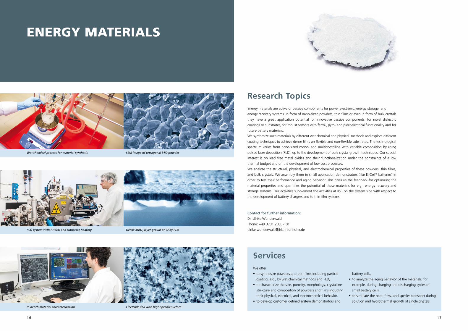
ENERGY MATERIALS
ServicesWe offer
• to synthesize powders and thin films including particle
coating, e.g., by wet chemical methods and PLD,
• to characterize the size, porosity, morphology, crystalline
structure and composition of powders and films including
their physical, electrical, and electrochemical behavior,
• to develop customer defined system demonstrators and
Research TopicsEnergy materials are active or passive components for power electronic, energy storage, and
energy recovery systems. In form of nano-sized powders, thin films or even in form of bulk crystals
they have a great application potential for innovative passive components, for novel dielectric
coatings or substrates, for robust sensors with ferro-, pyro- and piezoelectrical functionality and for
future battery materials.
We synthesize such materials by different wet chemical and physical methods and explore different
coating techniques to achieve dense films on flexible and non-flexible substrates. The technological
spectrum varies from nano-sized mono- and multicrystalline with variable composition by using
pulsed laser deposition (PLD), up to the development of bulk crystal growth techniques. Our special
interest is on lead free metal oxides and their functionalization under the constraints of a low
thermal budget and on the development of low cost processes.
We analyze the structural, physical, and electrochemical properties of these powders, thin films,
and bulk crystals. We assembly them in small application demonstrators (like El-Cell® batteries) in
order to test their performance and aging behavior. This gives us the feedback for optimizing the
material properties and quantifies the potential of these materials for e.g., energy recovery and
storage systems. Our activities supplement the activities at IISB on the system side with respect to
the development of battery chargers and to thin film systems.
battery cells,
• to analyze the aging behavior of the materials, for
example, during charging and discharging cycles of
small battery cells,
• to simulate the heat, flow, and species transport during
solution and hydrothermal growth of single crystals.
Contact for further information:
Dr. Ulrike Wunderwald
Phone: +49 3731 2033-101
Wet chemical process for material synthesis
PLD system with RHEED and substrate heating
In depth material characterization Electrode foil with high specific surface
Dense MnO2 layer grown on Si by PLD
SEM image of tetragonal BTO powder
1716
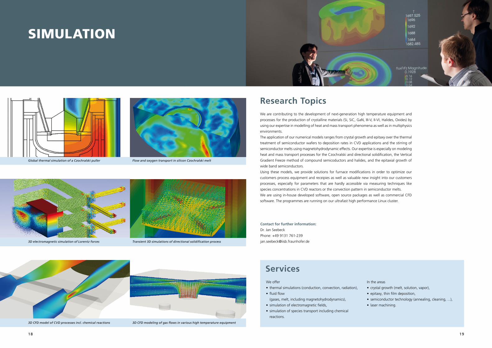
SIMULATION
Services We offer
• thermal simulations (conduction, convection, radiation),
• fluid flow
(gases, melt, including magnetohydrodynamics),
• simulation of electromagnetic fields,
• simulation of species transport including chemical
reactions.
Research TopicsWe are contributing to the development of next-generation high temperature equipment and
processes for the production of crystalline materials (Si, SiC, GaN, III-V, II-VI, Halides, Oxides) by
using our expertise in modelling of heat and mass transport phenomena as well as in multiphysics
environments.
The application of our numerical models ranges from crystal growth and epitaxy over the thermal
treatment of semiconductor wafers to deposition rates in CVD applications and the stirring of
semiconductor melts using magnetohydrodynamic effects. Our expertise is especially on modeling
heat and mass transport processes for the Czochralski and directional solidification, the Vertical
Gradient Freeze method of compound semicoductors and halides, and the epitaxial growth of
wide band semiconductors.
Using these models, we provide solutions for furnace modifications in order to optimize our
customers process equipment and receipies as well as valuable new insight into our customers
processes, especially for parameters that are hardly accessible via measuring techniques like
species concentrations in CVD reactors or the convection pattern in semiconductor melts.
We are using in-house developed software, open source packages as well as commercial CFD
software. The programmes are running on our ultrafast high performance Linux cluster.
In the areas
• crystal growth (melt, solution, vapor),
• epitaxy, thin film deposition,
• semiconductor technology (annealing, cleaning, ...),
• laser machining.
Contact for further information:
Dr. Jan Seebeck
Phone: +49 9131 761-239
Global thermal simulation of a Czochralski puller
3D CFD modeling of gas flows in various high temperature equipment
3D electromagnetic simulation of Lorentz forces
3D CFD model of CVD processes incl. chemical reactions
Flow and oxygen transport in silicon Czochralski melt
Transient 3D simulations of directional solidification process
1918
Recommended