Embed Size (px)
Citation preview
An Academic RISC-V Silicon ImplementationBased on Open-Source Components
Jaume Abella∗, Calvin Bulla∗, Guillem Cabo∗, Francisco J. Cazorla∗, Adrian Cristal∗, Max Doblas∗,Roger Figueras∗, Alberto Gonzalez∗, Carles Hernandez∗, Cesar Hernandez†, Vıctor Jimenez∗, Leonidas Kosmidis∗,
Vatistas Kostalabros∗, Ruben Langarita∗, Neiel Leyva†, Guillem Lopez-Paradıs∗, Joan Marimon∗,Ricardo Martınez‡, Jonnatan Mendoza∗, Francesc Moll§, Miquel Moreto∗§, Julian Pavon∗,Cristobal Ramırez∗, Marco A. Ramırez†, Carlos Rojas∗, Antonio Rubio§, Abraham Ruiz∗,
Nehir Sonmez∗, Vıctor Soria∗, Lluıs Teres‡, Osman Unsal∗, Mateo Valero∗§, Ivan Vargas∗, Luıs Villa†∗Barcelona Supercomputing Center (BSC), Barcelona, Spain. Email: [email protected]
†Centro de Investigacion en Computacion, Instituto Politecnico Nacional (CIC-IPN), Mexico City, Mexico.‡Instituto de Microelectronica de Barcelona, IMB-CNM (CSIC), Spain. Email: [email protected]
§Universitat Politecnica de Catalunya (UPC), Barcelona, Spain. Email: [email protected]
Abstract—The design presented in this paper, called preDRAC,is a RISC-V general purpose processor capable of booting Linuxjointly developed by BSC, CIC-IPN, IMB-CNM (CSIC), andUPC. The preDRAC processor is the first RISC-V processordesigned and fabricated by a Spanish or Mexican academicinstitution, and will be the basis of future RISC-V designs jointlydeveloped by these institutions. This paper summarizes the designtasks, for FPGA first and for SoC later, from high architecturallevel descriptions down to RTL and then going through logicsynthesis and physical design to get the layout ready for its finaltapeout in CMOS 65nm technology.
I. INTRODUCTION
Open-source software has represented a revolution in com-puting especially since the introduction of the Linux operatingsystem. More recently, open Instruction Set Architectures(ISA) have been proposed, with the promise of a similarrevolution in the hardware side, more specifically in the designof processors. Open ISAs offer the possibility to implementspecific microarchitectures suited for particular applications.
RISC-V is an open ISA originated in 2010 at the Uni-versity of California at Berkeley [1], and is now supportedby the RISC-V International [2] with hundreds of membersworldwide. RISC-V is composed of a base instruction setand extended in a modular fashion by a number of dedicatedinstruction extensions targeting higher performance or special-ized application domains.
Since the first public release of the RISC-V ISA, many im-plementations of processors have risen both from industry andacademia. PreDRAC is the first fabricated RISC-V processorfrom a Spanish or Mexican academic institution. This designwill be the first in a series of high performance computingprocessors designed in the context of the DRAC project
This is a Post-Print version of the paper published in DCIS 2020 by IEEE,DOI: 10.1109/DCIS51330.2020.9268664.
(Designing RISC-V-based Accelerators for next generationComputers), which started in June 2019.
This paper describes the design, verification, implementa-tion and post-silicon validation of a RISC-V general pur-pose processor capable of booting Linux. The design andverification process is described in the paper, starting withthe core and the rest of peripherals needed to implement aLinux-capable System-on-Chip (SoC), using open source andinternally designed Intellectual Property (IP) blocks.
The team for preDRAC (around 30 people from four dif-ferent institutions) was put together in January 2019 and thedesign development took place at three main design abstractionlevels: architectural, register transfer level (RTL) and physical;with most of the team dedicated to the architectural and RTLlevels. Verification efforts to ensure the integrity of the designbetween abstraction levels was also an essential part of thework.
The structure of the paper is as follows: Section II describesthe chip architecture and IP components. Section III explainsthe different pre- and post-fabrication verification techniques.Next, Section IV details the synthesis and physical designresults. Section V shows the measurements performed onthe manufactured chip. Finally, Section VI presents someconsiderations about the open source processors on silicon andconcludes this work.
II. CHIP ARCHITECTURE
The chip adapts an open-source SoC platform developedby lowRISC [3] for the Berkeley Rocket RISC-V core. Inthe preDRAC implementation, the core has been replaced byLagarto, a RISC-V processor core developed at CIC-IPN inMexico.
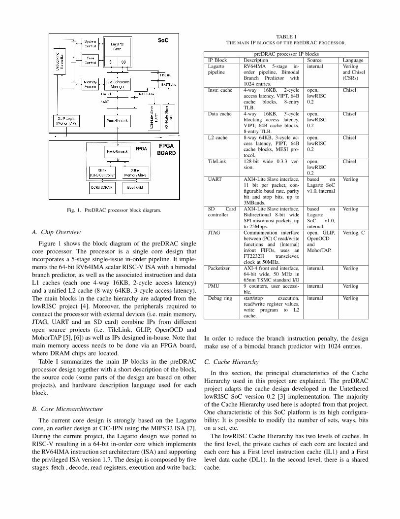
Fig. 1. PreDRAC processor block diagram.
A. Chip Overview
Figure 1 shows the block diagram of the preDRAC singlecore processor. The processor is a single core design thatincorporates a 5-stage single-issue in-order pipeline. It imple-ments the 64-bit RV64IMA scalar RISC-V ISA with a bimodalbranch predictor, as well as the associated instruction and dataL1 caches (each one 4-way 16KB, 2-cycle access latency)and a unified L2 cache (8-way 64KB, 3-cycle access latency).The main blocks in the cache hierarchy are adapted from thelowRISC project [4]. Moreover, the peripherals required toconnect the processor with external devices (i.e. main memory,JTAG, UART and an SD card) combine IPs from differentopen source projects (i.e. TileLink, GLIP, OpenOCD andMohorTAP [5], [6]) as well as IPs designed in-house. Note thatmain memory access needs to be done via an FPGA board,where DRAM chips are located.
Table I summarizes the main IP blocks in the preDRACprocessor design together with a short description of the block,the source code (some parts of the design are based on otherprojects), and hardware description language used for eachblock.
B. Core Microarchitecture
The current core design is strongly based on the Lagartocore, an earlier design at CIC-IPN using the MIPS32 ISA [7].During the current project, the Lagarto design was ported toRISC-V resulting in a 64-bit in-order core which implementsthe RV64IMA instruction set architecture (ISA) and supportingthe privileged ISA version 1.7. The design is composed by fivestages: fetch , decode, read-registers, execution and write-back.
TABLE ITHE MAIN IP BLOCKS OF THE PREDRAC PROCESSOR.
preDRAC processor IP blocksIP Block Description Source LanguageLagartopipeline
RV64IMA 5-stage in-order pipeline, BimodalBranch Predictor with1024 entries.
internal Verilogand Chisel(CSRs)
Instr. cache 4-way 16KB, 2-cycleaccess latency, VIPT, 64Bcache blocks, 8-entryTLB.
open,lowRISC0.2
Chisel
Data cache 4-way 16KB, 3-cycleblocking access latency,VIPT, 64B cache blocks,8-entry TLB.
open,lowRISC0.2
Chisel
L2 cache 8-way 64KB, 3-cycle ac-cess latency, PIPT, 64Bcache blocks, MESI pro-tocol.
open,lowRISC0.2
Chisel
TileLink 128-bit wide 0.3.3 ver-sion.
open,lowRISC0.2
Chisel
UART AXI4-Lite Slave interface,11 bit per packet, con-figurable baud rate, paritybit and stop bits, up to3MBauds.
based onLagarto SoCv1.0, internal
Verilog
SD Cardcontroller
AXI4-Lite Slave interface,Bidirectional 8-bit wideSPI miso/mosi packets, upto 25Mbps.
based onLagartoSoC v1.0,internal.
Verilog
JTAG Communication interfacebetween (PC) C read/writefunctions and (Internal)in/out FIFOs, uses anFT2232H transciever,clock at 50MHz.
open, GLIP,OpenOCDandMohorTAP.
Verilog, C
Packetizer AXI-4 front end interface,64-bit wide, 50 MHz in65nm TSMC standard I/O
internal. Verilog
PMU 9 counters, user accessi-ble.
internal Verilog
Debug ring start/stop execution,read/write register values,write program to L2cache.
internal Verilog
In order to reduce the branch instruction penalty, the designmake use of a bimodal branch predictor with 1024 entries.
C. Cache Hierarchy
In this section, the principal characteristics of the CacheHierarchy used in this project are explained. The preDRACproject adapts the cache design developed in the UntetheredlowRISC SoC version 0.2 [3] implementation. The majorityof the Cache Hierarchy used here is adopted from that project.One characteristic of this SoC platform is its high configura-bility: It is possible to modify the number of sets, ways, bitson a set, etc.
The lowRISC Cache Hierarchy has two levels of caches. Inthe first level, the private caches of each core are located andeach core has a First level instruction cache (IL1) and a Firstlevel data cache (DL1). In the second level, there is a sharedcache.
In the first level, the caches are Virtually Indexed PhysicallyTagged (VIPT). This means that the index used to accessthe metadata or data arrays are the virtual ones, but insidethe metadata array, the saved tags are the physical ones.This configuration allows to access the Translation LookasideBuffer (TLB) in parallel with the metadata and data arrays,making the critical path shorter. The only requirement toimplement this type of cache is that the page size must bea multiple of the cache way size. For instance, given that DL1and IL1 cache way size is 4 kB, VIPT is feasible for pagesizes of 4×N kB.
In this hierarchy, the caches are inclusive. In this case, thismeans that in the second level cache (L2) there is an activecopy of all the data that are in the first-level caches. Thatimplies the need to invalidate all the copies in the first levelcache of each line evicted from the L2. LowRISC implementsa variety of coherence protocols. In the preDRAC tapeout, theprotocol chosen is MESI. In this case, a directory is used tomaintain the coherence. This directory is located in the lastlevel of cache, the L2.
The replacement mechanism used in the lowRISC cachescan only be random replacement. Therefore, on the preDRACSoC, all the caches are using random replacement protocol.This random replacement uses the lower bits of a 16 bits LFSRin order to select the next set to be replaced. The feedbackpolynomial is:
x16 + x14 + x13 + x11 + 1 (1)
D. Access to Main Memory and Peripherals
Ideally, the objective of the tapeout would be to include thewhole preDRAC SoC, together with all the aforementionedperipherals on a single die. However, we faced many chal-lenges regarding the availability of certain technologies andanalog and digital IPs that are needed for fabrication.
The lack of a physical interface for a DDR3 memorycontroller motivated us to design a custom interface to commu-nicate with memory using the physical DDR3 memory froman external FPGA board, in our case a Xilinx Kintex KC705.
This implied to split the original design into two parts,one that contains the memory controllers to access the mainmemory, and a second one containing the core and rest ofthe uncore system, including L1 and L2 cache memories.Both parts are connected with an FPGA Mezzanine Card(FMC) cable. This split is depicted in Figure 1. This externalconnection only supports up to 50 MHz transfer speed, andalso the 128-bit bus must be split into 4 transactions of 32 bitseach.
E. Clocking
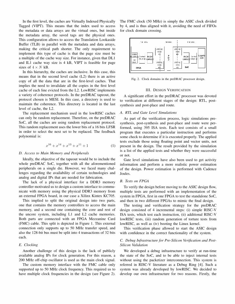
Another challenge of this design is the lack of publiclyavailable analog IPs for clock generation. For this reason, a200 MHz off-chip oscillator is used as the main clock signal.
The custom memory interface with the FMC cable onlysupported up to 50 MHz clock frequency. This required us tohave multiple clock frequencies in the design (see Figure 2).
The FMC clock (50 MHz) is simply the ASIC clock dividedby 4, and is thus aligned with it, avoiding the need of FIFOsfor clock domain crossing.
Fig. 2. Clock domains in the preDRAC processor design.
III. DESIGN VERIFICATION
A significant effort in the preDRAC processor was devotedto verification at different stages of the design: RTL, post-synthesis and post-place and route.
A. RTL and Gate Level Simulations
As part of the verification process, logic simulations pre-synthesis, post-synthesis and post-place and route were per-formed, using 395 ISA tests. Each test consists of a smallprogram that executes a particular instruction and performssome check to determine if it is executed properly. The appliedtests exclude those using floating point and vector units, notpresent in the design. The result provided by the simulationis a list of the applied tests and whether they were successfulor not.
Gate level simulations have also been used to get activityinformation and perform a more realistic power estimationof the design. Power estimation is performed with CadenceJoules.
B. Tests on FPGA
To verify the design before moving to the ASIC design flow,multiple tests are performed with an implementation of thesystem in FPGA, first in one FPGA to test the standalone SoC,and then in two different FPGAs to mimic the final design.
The testing and verification strategy for the preDRACdesign consisted of 4 incremental steps: (i) simple RISC-VISA tests, which test each instruction, (ii) additional RISC-VlowRISC tests, (iii) random generation of torture tests fromlowRISC, as well as (iv) booting the Linux kernel.
This verification phase allowed to start the ASIC designwith confidence in the correct functionality of the system.
C. Debug Infrastructure for Pre-Silicon Verification and Post-Silicon Validation
We developed a debug infrastructure to verify at run-timethe state of the SoC, and to be able to inject internal testswithout using the packetizer interconnection. This system isreferred in RISC-V literature as a Debug Ring [4]. Such asystem was already developed by lowRISC. We decided todevelop our own infrastructure for two reasons. Firstly, the
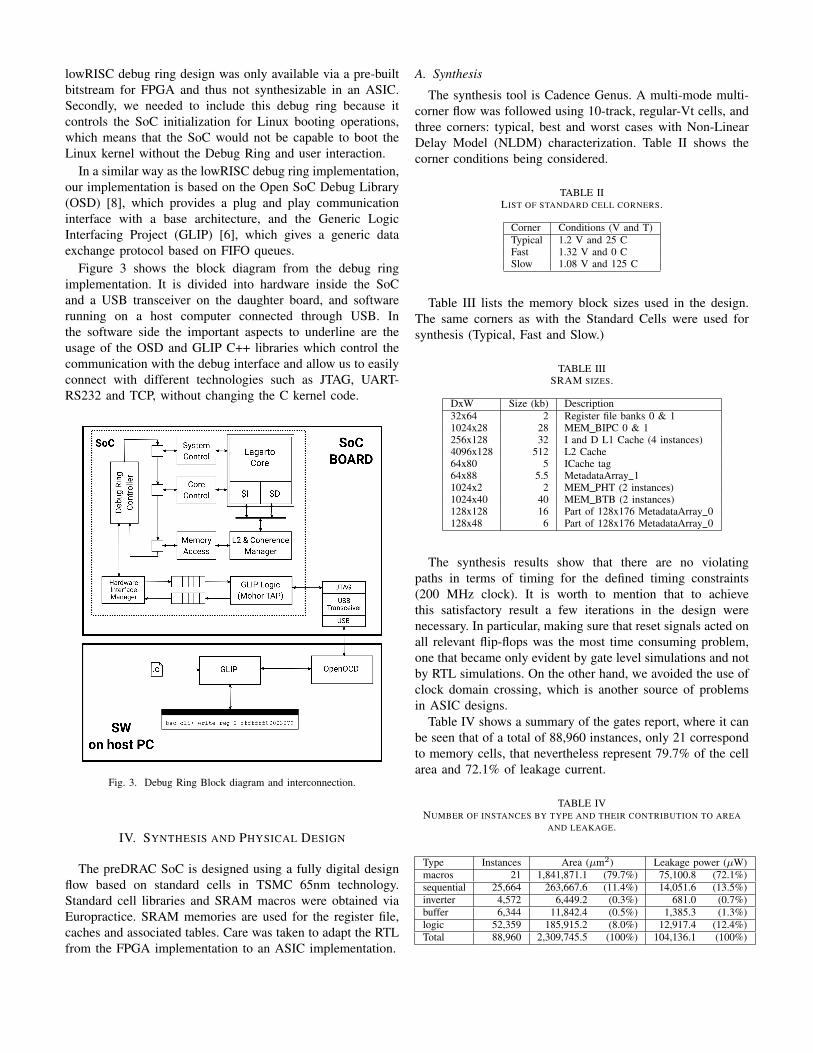
lowRISC debug ring design was only available via a pre-builtbitstream for FPGA and thus not synthesizable in an ASIC.Secondly, we needed to include this debug ring because itcontrols the SoC initialization for Linux booting operations,which means that the SoC would not be capable to boot theLinux kernel without the Debug Ring and user interaction.
In a similar way as the lowRISC debug ring implementation,our implementation is based on the Open SoC Debug Library(OSD) [8], which provides a plug and play communicationinterface with a base architecture, and the Generic LogicInterfacing Project (GLIP) [6], which gives a generic dataexchange protocol based on FIFO queues.
Figure 3 shows the block diagram from the debug ringimplementation. It is divided into hardware inside the SoCand a USB transceiver on the daughter board, and softwarerunning on a host computer connected through USB. Inthe software side the important aspects to underline are theusage of the OSD and GLIP C++ libraries which control thecommunication with the debug interface and allow us to easilyconnect with different technologies such as JTAG, UART-RS232 and TCP, without changing the C kernel code.
Fig. 3. Debug Ring Block diagram and interconnection.
IV. SYNTHESIS AND PHYSICAL DESIGN
The preDRAC SoC is designed using a fully digital designflow based on standard cells in TSMC 65nm technology.Standard cell libraries and SRAM macros were obtained viaEuropractice. SRAM memories are used for the register file,caches and associated tables. Care was taken to adapt the RTLfrom the FPGA implementation to an ASIC implementation.
A. Synthesis
The synthesis tool is Cadence Genus. A multi-mode multi-corner flow was followed using 10-track, regular-Vt cells, andthree corners: typical, best and worst cases with Non-LinearDelay Model (NLDM) characterization. Table II shows thecorner conditions being considered.
TABLE IILIST OF STANDARD CELL CORNERS.
Corner Conditions (V and T)Typical 1.2 V and 25 CFast 1.32 V and 0 CSlow 1.08 V and 125 C
Table III lists the memory block sizes used in the design.The same corners as with the Standard Cells were used forsynthesis (Typical, Fast and Slow.)
TABLE IIISRAM SIZES.
DxW Size (kb) Description32x64 2 Register file banks 0 & 11024x28 28 MEM BIPC 0 & 1256x128 32 I and D L1 Cache (4 instances)4096x128 512 L2 Cache64x80 5 ICache tag64x88 5.5 MetadataArray 11024x2 2 MEM PHT (2 instances)1024x40 40 MEM BTB (2 instances)128x128 16 Part of 128x176 MetadataArray 0128x48 6 Part of 128x176 MetadataArray 0
The synthesis results show that there are no violatingpaths in terms of timing for the defined timing constraints(200 MHz clock). It is worth to mention that to achievethis satisfactory result a few iterations in the design werenecessary. In particular, making sure that reset signals acted onall relevant flip-flops was the most time consuming problem,one that became only evident by gate level simulations and notby RTL simulations. On the other hand, we avoided the use ofclock domain crossing, which is another source of problemsin ASIC designs.
Table IV shows a summary of the gates report, where it canbe seen that of a total of 88,960 instances, only 21 correspondto memory cells, that nevertheless represent 79.7% of the cellarea and 72.1% of leakage current.
TABLE IVNUMBER OF INSTANCES BY TYPE AND THEIR CONTRIBUTION TO AREA
AND LEAKAGE.
Type Instances Area (µm2) Leakage power (µW)macros 21 1,841,871.1 (79.7%) 75,100.8 (72.1%)sequential 25,664 263,667.6 (11.4%) 14,051.6 (13.5%)inverter 4,572 6,449.2 (0.3%) 681.0 (0.7%)buffer 6,344 11,842.4 (0.5%) 1,385.3 (1.3%)logic 52,359 185,915.2 (8.0%) 12,917.4 (12.4%)Total 88,960 2,309,745.5 (100%) 104,136.1 (100%)
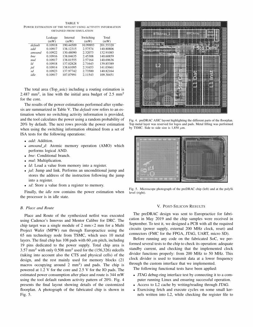
TABLE VPOWER ESTIMATION OF THE NETLIST USING ACTIVITY INFORMATION
OBTAINED FROM SIMULATION
Leakage Internal Switching Total(mW) (mW) (mW) (mW)
default 0.10918 190.44509 10.99893 201.55320add 0.10917 138.12315 2.57574 140.80806amoand 0.10922 130.48090 2.32073 132.91085bne 0.10916 138.04635 2.45308 140.60859mul 0.10917 138.01555 2.57164 140.69636ld 0.10918 137.02828 2.71643 139.85389jal 0.10914 138.61095 2.31653 141.03661sd 0.10923 137.97742 2.73500 140.82164idle 0.10917 107.07991 2.11543 109.30451
The total area (Top asic) including a routing estimation is2.487 mm2, in line with the initial area budget of 2.5 mm2
for the core.The results of the power estimations performed after synthe-
sis are summarized in Table V. The default row refers to an es-timation where no switching activity information is provided,and the tool calculates the power using a random probability of20% by default. The next rows provide the power estimationwhen using the switching information obtained from a set ofISA tests for the following operations:
• add: Addition.• amoand d: Atomic memory operation (AMO) which
performs logical AND.• bne: Conditional branch.• mul: Multiplication.• ld: Load a value from memory into a register.• jal: Jump and link. Performs an unconditional jump and
stores the address of the instruction following the jumpinto a register.
• sd: Store a value from a register to memory.
Finally, the idle row contains the power estimation whenthe processor is in idle state.
B. Place and Route
Place and Route of the synthesized netlist was executedusing Cadence’s Innovus and Mentor Calibre for DRC. Thechip target was a single module of 2 mm×2 mm for a MultiProject Wafer (MPW) run through Europractice using the65 nm technology node from TSMC, which uses 10 metallayers. The final chip has 108 pads with 60 µm pitch, including19 pins dedicated to the power supply. Total chip area is3.57 mm2 with only 0.508 mm2 used for the (156,326) stdcells(taking into account also the CTS and physical cells) of thedesign, and the rest mainly used for memory blocks (21macros occupying around 2 mm2) and pads. The chip ispowered at 1.2 V for the core and 2.5 V for the IO pads. Theestimated power consumption after place and route is 344 mWusing the tool default random activity pattern of 20%. Fig. 4presents the final layout showing details of the customizedfloorplan. A photograph of the fabricated chip is shown inFig. 5.
L2
L1
Dat
L1
Inst
MDArray_tag_A
MDArray_tag_1
MDArray_tag_B
IC_tag_array
PHTArrayBTBArray_1 BIPCArray
RFA
rray
Std
Cells
Std Cells
Fig. 4. preDRAC ASIC layout highlighting the different parts of the floorplan.Top metal layer was reserved for logos and pads. Metal filling was performedby TSMC. Side to side size is 1,850 µm.
Fig. 5. Microscope photograph of the preDRAC chip (left) and at the polySilevel (right).
V. POST-SILICON RESULTS
The preDRAC design was sent to Europractice for fabri-cation in May 2019 and the chip samples were received inSeptember. To test it, we designed a PCB with all the requiredcircuits (power supply, external 200 MHz clock, reset) andconnectors (FMC for the FPGA, JTAG, UART, micro SD).
Before running any code on the fabricated SoC, we per-formed several tests to the chip to check its operation: adequatestandby current, and checking that the implemented clockdivider functions properly: from 200 MHz to 50 MHz. Thisclock divider is used to transmit data at a lower frequencythrough the custom interface that we implemented.
The following functional tests have been applied:
• JTAG debug-ring interface test by connecting it to a com-puter running Linux and ensuring successful operation.
• Access to L2 cache by writing/reading through JTAG.• Exercising fetch and execute cycles on some small ker-
nels written into L2, while checking the register file to
verify the correct code execution.• Running a set of ISA tests to verify the correctness of
individual instructions.• Running a subset of Malardalen WCET Benchmarks [9]
to get some average performance numbers: IPC of 0.33with a clock frequency of 200 MHz. These are bare-metalapplications stored on the FPGA BootRAM and accessedvia the Packetizer.
• Finally, we tested different SoC peripherals (UART, SPI,PMU and DDR3) from kernels loaded into main memoryusing the custom interface.
Results of above tests concluded that all of them worked asexpected, except for the SPI controller, which shows a buggybehaviour and prevented the use of the on-board SD card.As a workaround to this issue, we implemented an alternativepath to access the peripherals using the custom interface. Wemoved the UART and the SPI controllers to the FPGA side,and the SoC uses the custom interface to access them. In thisway, we were able to use the external SD card memory andsuccessfully boot Linux.
VI. CONCLUSIONS AND FUTURE WORK
RISC-V open ISA is a great opportunity for educational,research and industry organizations to work on open pro-cessor based developments while opening many potentialcollaborations among these communities. It is expected thatthis new drive will also impact other hardware developmentdomains other than just processors. Different organizations likeOpenHW Group [10], CHIPS Alliance [11], FOSSi Founda-tion [12] or local networks as RISC-V France [13] and Red-RISCV [14], in addition to the parent organization RISC-V International [2], are working on a collaborative schemetowards this new open hardware paradigm and opportunities.Europe has also decided to work on this direction by applyingopen-source HW/SW to avoid excessive technology dependen-cies from third parties, firms or countries, and has chosen theRISC-V ISA as the base-line architecture for next Europeanprocessors [15].
In this design experience, it was possible to assess theexisting resources and limitations of the open-source proposalregarding processor ASIC design.
Many resources do exist, and some of them were indeedleveraged for this project. Processor design may use open-source RTL cores and resources for SoC (e.g. lowRISC,PULP [16]).
It is also true that porting a processor to silicon impliesa large effort and currently there are some technical andeconomic hurdles to surmount that prevent this activity to be amainstream one like: in depth knowledge of specialized designflows, expensive and proprietary EDA tools, limited or costlyaccess to libraries, memory macros and analog IPs.
Some of these limitations are alleviated by the Europracticeprogram in the case of academic and research institutes,which have access to low cost CAD tools, libraries andmanufacturing. In the case of analog IPs for silicon there isnot a straightforward solution, although some efforts, such as
the Berkeley Analog Generator approach [17], [18] go in thedirection to offer open-source analog blocks as well.
In 2020 we plan to fabricate a new iteration of the preDRACdesign incorporating more robust verification methodologiesand multiple IPs (i.e. a PLL or a new interface with memory),opening the door to future high performance designs.
Once this updated design is being fabricated and tested, weplan to prepare the Lagarto RISC-V core to be offered as freeand open-source hardware.
ACKNOWLEDGMENTS
The DRAC project is co-financed by the European UnionRegional Development Fund within the framework of theERDF Operational Program of Catalonia 2014-2020 with agrant of 50% of total eligible cost. The authors are part of Red-RISCV which promotes activities around open hardware. TheLagarto Project is supported by the Research and GraduateSecretary (SIP) of the Instituto Politecnico Nacional (IPN)from Mexico, and by the CONACyT scholarship for Centerfor Research in Computing (CIC-IPN).
REFERENCES
[1] Andrew Waterman, Yunsup Lee, David A. Patterson, and KrsteAsanovic. “The RISC-V Instruction Set Manual, Volume I: Base User-Level ISA”. In Tech. Report UCB/EECS-2011-62, EECS Dept., UCBerkeley, pages 97–116, 2011.
[2] RISC-V International. https://riscv.org/. [Online; accessed 23-April-2020].
[3] lowRISC. “Untethered lowRISC v0.2”. https://www.lowrisc.org/docs/untether-v0.2/. [Online; accessed 27-August-2019].
[4] lowRISC. “Overview of the debug infrastructure”. https://www.lowrisc.org/docs/debug-v0.3/overview/, 2018.
[5] U. C. Berkeley. “The TileLink Specification, Version 0.3.3”. https://docs.google.com/document/d/1Iczcjigc-LUi8QmDPwnAu1kH4Rrt6Kqi1EUaCrfrk8. [Online; accessed 23-July-2019].
[6] Institute for Integrated Systems (LIS). “The Generic Logic InterfacingProject”. https://www.glip.io/index.html, 2018.
[7] Cristobal Ramırez, Cesar Hernandez, Carlos Rojas Morales, Gus-tavo Mondragon Garcıa, Luıs A. Villa, and Marco A. Ramırez. “LagartoI–Una plataforma hardware/software de arquitectura de computadoraspara la academia e investigacion”. In Research in Computing Science,volume 137, pages 19–28, 2017.
[8] The Open SoC Debug Contributors. “The Open SoC Debug Docu-mentation Library”. https://opensocdebug.readthedocs.io/en/latest/index.html#, 2018.
[9] “Malardalen WCET benchmarks homepage”. www.mrtc.mdh.se/projects/wcet/benchmarks.html, 2010. [Online; accessed 4-September-2019].
[10] Open Hardware Group. https://www.openhwgroup.org/. [Online; ac-cessed 23-April-2020].
[11] CHIPS Alliance. https://chipsalliance.org/. [Online; accessed 23-April-2020].
[12] FOSSi Foundation. https://fossi-foundation.org/. [Online; accessed 23-April-2020].
[13] RISC-V France. https://www.riscv.fr/. [Online; accessed 23-April-2020].[14] Red RISC-V. https://www.red-riscv.org/. [Online; accessed 23-April-
2020].[15] European Processor Initiative. https://www.
european-processor-initiative.eu/. [Online; accessed 23-April-2020].[16] PULP Platform. https://pulp-platform.org/. [Online; accessed 23-April-
2020].[17] J. Crossley, A. Puggelli, H. P. Le, B. Yang, R. Nancollas, K. Jung,
L. Kong, N. Narevsky, Y. Lu, N. Sutardja, E. J. An, A. L. Sangiovanni-Vincentelli, and E. Alon. “BAG: A designer-oriented integrated frame-work for the development of AMS circuit generators”. In IEEE/ACMInternational Conference on Computer-Aided Design, Digest of Techni-cal Papers, ICCAD, pages 74–81, 2013.

[18] Eric Chang, Jaeduk Han, Woorham Bae, Zhongkai Wang, NathanNarevsky, Borivoje NikoliC, and Elad Alon. “BAG2: A process-portableframework for generator-based AMS circuit design”. In 2018 IEEECustom Integrated Circuits Conference (CICC), pages 1–8. IEEE, apr2018.