Embed Size (px)
Citation preview
ISSN: 2237-0722
Vol. 11 No. 2 (2021)
Received: 12.04.2021 – Accepted: 04.05.2021
2221
Design and Implementation of Single Phase to Three Phase Drive System Using
Space Vector Modulation
Manikandan Ganesan1; K.R. Ishwarya2; Demoz Lisanework3; Ganesh Babu Loganathan4 1Department of Electromechanical Engineering, Faculty of Manufacturing, Institute of Technology, Hawassa
University, Hawassa, Ethiopia. [email protected]
2Department of Electromechanical Engineering, Faculty of Manufacturing, Institute of Technology, Hawassa
University, Hawassa, Ethiopia. [email protected]
3Head, Department of Electromechanical Engineering, Faculty of Manufacturing, Institute of Technology,
Hawassa University, Hawassa, Ethiopia. [email protected]
4Department of Mechatronics Engineering, Tishk International University, Erbil, KRG, Iraq. [email protected]
Abstract
This paper discusses about the transformation of 1Φ to 3Φ drive system. Generally, the distribution of
electric power is typically three phase, however, when it is distributed to suburban areas, small scale
industries and rural areas it is single phase. This proposed system was developed by using MATLAB
Simulink Model and Hardware Implementation. It describes various conversion techniques such as AC
to DC conversion using single phase rectifier, DC to DC conversion by using boost converter, DC to
Three phase AC by using space vector modulation inverter. Besides software, hardware system was
also developed to control the 3Φ asynchronous motor and its performance was successfully obtained.
Key-words: Single-phase Grid, Switching Time, Static Power Converter, Total Hormonic Distortion.
1. Introduction
While comparing with 1Φ induction motor, the 3Φ induction motor has high power factor,
consumes less energy, high starting torque, torque ripples are less, high efficiency and smaller in size
for the same power rating. Generally the single phase wirings are used in our home appliances. Hence
a compatible 1Φ to 3Φ converter is essential to use 3Φ motor in single phase grid to conserve energy

ISSN: 2237-0722
Vol. 11 No. 2 (2021)
Received: 12.04.2021 – Accepted: 04.05.2021
2222
and to overcome the draw backs of single phase motors. [1] illustrated that effect of power ripple was
double the time of grid frequency which is the major problem while converting from 1Φ to 3Φ [2].
Implemented the control approach which has been developed by using fixed-point DSP-based
controller ADMC 401 to improve power quality for unbalanced and nonlinear loads. Suggested that
the input converter topology can decrease the harmonic distortion and rectifier switching currents [3].
Derived a system model for reducing the circulating current which is used to decrease the total energy
loss [4]. Developed voltage to frequency controller using TMS320C31 digital signal processor to
eliminate the dc-link voltage ripples for asynchronous motor drives [5]. For various load conditions the
bi-directional AC- AC converter was implemented by Yang, Proposed PWM based voltage source
inverter and it functions as both active filter and voltage compensator depending upon the PCC drop
voltage range [6,7]. To obtain the high power efficiency, cost effective and reliable system, the less
numbers of advanced semiconductor devices were used by Developed the control strategies for both
transformers less and transformer-based topologies [8,9]. Without transformer designed a 1Φ rectifier
which has two parallel 1Φ halfwave converter [10]. Experimented the system to decrease the circulating
currents without isolation transformer [11-13]. The present paper describes the space vector modulation
(SVM) technique to convert 1Φ to 3Φ system instead of the PWM inverter technique which was widely
used [14-17]. To suppress the harmonics, the SVM technique is utilized to produce the required
switching pulses in order to achieve various modulation indexes[18-22].
2. Methodology
The 1Φ to 3Φ systems consist of following conversion stages and they are:
AC to DC Conversion (Single Phase Rectifier).
DC to DC Conversion (Boost Converter).
DC to AC Conversion (Voltage Source Inverter using SVM).
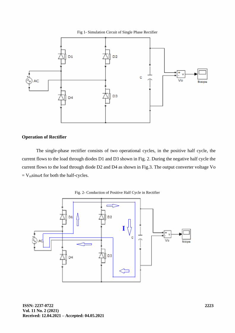
AC to DC Conversion (Single Phase Rectifier)
The single-phase sinusoidal voltage is converted into constant DC voltage by using 1Φ bridge
rectifier. The circuit diagram of the 1Φ rectifier is shown in Fig. 1.
ISSN: 2237-0722
Vol. 11 No. 2 (2021)
Received: 12.04.2021 – Accepted: 04.05.2021
2223
Fig 1- Simulation Circuit of Single Phase Rectifier
Operation of Rectifier
The single-phase rectifier consists of two operational cycles, in the positive half cycle, the
current flows to the load through diodes D1 and D3 shown in Fig. 2. During the negative half cycle the
current flows to the load through diode D2 and D4 as shown in Fig.3. The output converter voltage Vo
= Vmsin𝜔t for both the half-cycles.
Fig. 2- Conduction of Positive Half Cycle in Rectifier

ISSN: 2237-0722
Vol. 11 No. 2 (2021)
Received: 12.04.2021 – Accepted: 04.05.2021
2224
Fig. 3- Conduction of Negative Half Cycle in Conduction of Rectifier
The average output value of positive half cycle is:
For0 < 𝜔𝑡 < 𝜋
𝑉0 = √2𝑉𝑖 sin 𝜔𝑡 (1)
The average output value of negative half cycle is given by
For𝜋 < 𝜔𝑡 < 2𝜋
𝑉0 = √2𝑉𝑖 sin 𝜔𝑡 (2)
The total average output value is given as
𝑉0𝐴𝑉 =1
𝜋∫ √2
𝜋
0𝑉𝑖
2 sin 𝜔𝑡 𝑡 𝜔𝑡 =2√2
𝜋𝑉𝑖 (3)
The RMS value of output is:
𝑉0𝑅𝑀𝑆 = √1
𝜋∫ 2𝑉𝑖
2𝜋
0𝑠𝑖𝑛2𝜔𝑡 𝑑 𝜔 (4)
The output of single phase full wave rectifier is not a pure DC voltage. In order to obtain the
ripple free DC voltage the capacitive filter is added across load.
DC to DC Conversion (Boost Converter)
The boost converter is used to step up the DC 230 volts into high level DC volts in the range of
1000 volts. The simulation circuit diagram is shown in Fig. 4.

ISSN: 2237-0722
Vol. 11 No. 2 (2021)
Received: 12.04.2021 – Accepted: 04.05.2021
2225
Fig. 4- Simulation Circuit of Boost Converter
The DC- DC boost converter has two different operational modes which relies switching period
length and energy storage capacity. The former and latter modes depend on the Pulse width of switch
gate signal and Value of Inductance respectively [23-27]. The inductance and capacitance values are
calculated based on following equations.
Lc =RD(1−D)2
2F (5)
𝐶𝑏 =𝑉0𝐷
𝐹∆𝑉0𝑅 (6)
Where,
Vo- Output Voltage
F- Switching frequency
D- Duty Cyle
R- Load Resistance
DC to AC Conversion (Voltage Source Inverter Using SVM)
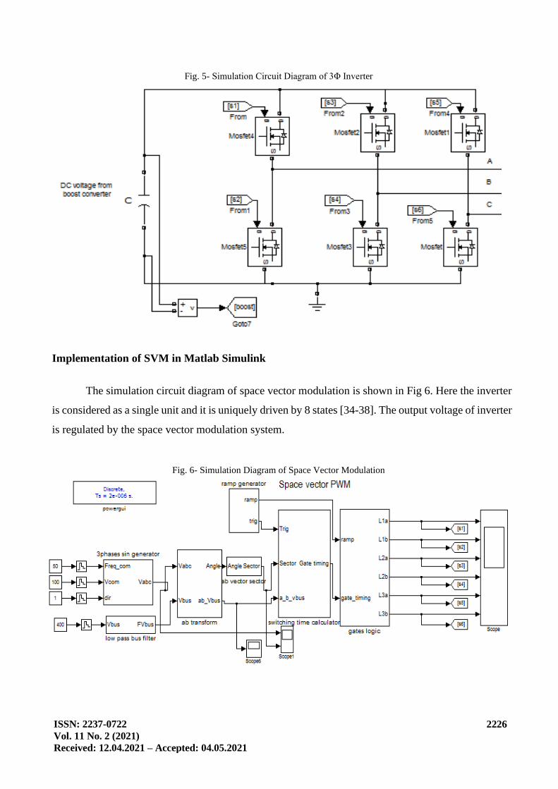
The three phase inverter is designed by connecting three single phase inverters in parallel. In
this, the input pulse to the gate signals of each phase have difference of 120o. These inverters drawn
Input DC supply from a Booster converter. Fig. 2.5 shows the simulation circuit diagram of 3Φ inverter
using six MOSFET’s [28-33]. To achieve constant DC input voltage the high value of capacitor was
connected across the input terminals and it putdowns the harmonics of the source.
ISSN: 2237-0722
Vol. 11 No. 2 (2021)
Received: 12.04.2021 – Accepted: 04.05.2021
2226
Fig. 5- Simulation Circuit Diagram of 3Φ Inverter
Implementation of SVM in Matlab Simulink
The simulation circuit diagram of space vector modulation is shown in Fig 6. Here the inverter
is considered as a single unit and it is uniquely driven by 8 states [34-38]. The output voltage of inverter
is regulated by the space vector modulation system.
Fig. 6- Simulation Diagram of Space Vector Modulation

ISSN: 2237-0722
Vol. 11 No. 2 (2021)
Received: 12.04.2021 – Accepted: 04.05.2021
2227
Sampling depends on the proper selection of states for each switch and its respective time
duration [39,40]. Hence there are eight possible switching vector combinations are available in the
orthogonal plane, only six non-zero switching vectors are used, it forms a hexagon which is shown in
Fig.7 cited in [13].
Fig. 7- Vector Representation of Space Vector Modulation [13]
Modulation Scheme
The following procedures are required to develop space vector modulation:
• Initially, the reference vector Vref obtained by mapping the orthogonal d-q coordinates from the
reference signals of phase A, B and C.
• Secondly, in order to get one switching cycle the zero and non zero switching vectors are
combined for Vref

ISSN: 2237-0722
Vol. 11 No. 2 (2021)
Received: 12.04.2021 – Accepted: 04.05.2021
2228
• Next, by implementing a simple trigonometric algorithm, selected switching vectors time
durations are calculated.
• Finally, the switching network receives sequenced switching pulses.
Conversion Algorithm
Step 1: Consider the respective 3Φ reference voltages (Va,Vb, Vc)
Step 2: Two-phase transformation is mapped from three-phase vectors
Step 3: Determine absolute value of Vd,Vq and arctangent (Vd/Vq)
Step 4: The sector must be identified where the source vector voltage is available.
Step 5: The switching vectors are selected from the respective identified sector.
Step 6: The calculation of switching times relies on the vector magnitude value of output voltage
Step 7: According to the sequencing scheme the switching vectors are obtained
Step 8: The Control signals are delivered to the switching network of each phase.
Step 9: Thus, the load terminals of voltage source inverter provide the required output.
3. Hardware Implementation of 1Φ to 3Φ Conversion
The source voltage of 220V AC is supplied to input of the transformer. The transformer is used
to step-down the voltage from an AC voltage of 220V to 24V and 24V is given to the bridge rectifiers.
Thus, the AC voltage rectified to rippled DC voltage. The capacitor is connected across the rectifier as
a filter in order to minimize the ripples. The three-phase inverter is driven by the driver circuit with an
angle of 120° mode. In this microcontroller 89C51 controls the gate signals.
The constant DC voltage as the input supply of micro controller (5V dc) is obtained by a circuit
which consists of rectifier (40W, 300V, 1A), capacitors (1000 F, 25PF). The drive circuit consists of
Opto-coupler which is used to isolate the circuits of micro controller. The step-down transformer
(230/12) V providing input supply to the drive circuits. The each MOSFET receives 12V gate single
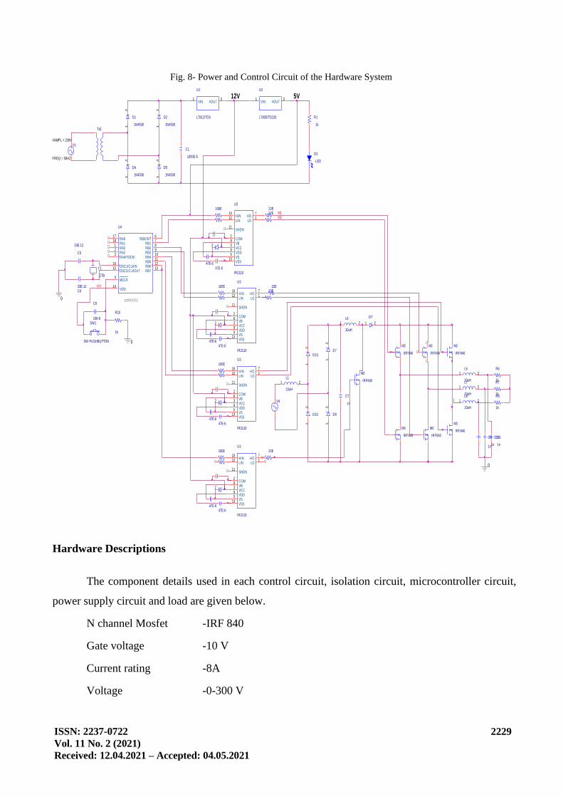
from the driver circuit to control the ON and OFF time duration of each MOSFET. The power and
control circuit of the hardware system is shown in Fig 8.
ISSN: 2237-0722
Vol. 11 No. 2 (2021)
Received: 12.04.2021 – Accepted: 04.05.2021
2229
Fig. 8- Power and Control Circuit of the Hardware System
Hardware Descriptions
The component details used in each control circuit, isolation circuit, microcontroller circuit,
power supply circuit and load are given below.
N channel Mosfet -IRF 840
Gate voltage -10 V
Current rating -8A
Voltage -0-300 V
M3
IRF840
C8
10E-6
47E-6
C10
1n
12V
100E
100E
V4
47E-6
47E-6
M3
IRF840
V1
FREQ = 50HZ
VAMPL = 230V
R8
1k
D10
12
22E
L1
10uH
1 2
SW1
SW PUSHBUTTON
47E-6
+5V
47E-6
R6
1k
R1
1k
D7
1 2
U3
IR2110
1710
11
12
13
26395
LOHOHIN
SHDN
LIN
VSS
COMVBVCCVDDVS
TX1
22E
C5
33E-12
100E
C7
1n
U3
IR2110
1710
11
12
13
26395
LOHOHIN
SHDN
LIN
VSS
COMVBVCCVDDVS
47E-6Y1
ZTB
C1
1000E-6
D10
12
L6
10uH
1 2
L8
10uH
1 2
M1
D5
1N4500
12
M3
IRF840
12
M3
IRF840
U3
IR2110
1710
11
12
13
26395
LOHOHIN
SHDN
LIN
VSS
COMVBVCCVDDVS
D4
1N4500
12
12
U1
L7812/TO3
1 2VIN VOUT
U3
IR2110
1710
11
12
13
26395
LOHOHIN
SHDN
LIN
VSS
COMVBVCCVDDVS
C9
1n
0
D3
LED
AT89C2051
0
47E-6
L7
10uH
1 2
L6
10uH
1 2
D1
1N45001
2
D7
12
M3
IRF840
47E-6
U4
14
15
4
16
1718123
678910111213
VDD
OSC2/CLKOUT
MCLR
OSC1/CLKIN
RA0RA1RA2RA3RA4/TOCKI
RB0/INTRB1RB2RB3RB4RB5RB6RB7
M3
IRF840
0
22E
12
R7
1k
C11
1n
100E
22EM2
M3
IRF840
D8
12
22E
C633E-12
R10
1k
5V
12
D2
1N4500
12
U2
L7805/TO220
1 2VIN VOUT
ISSN: 2237-0722
Vol. 11 No. 2 (2021)
Received: 12.04.2021 – Accepted: 04.05.2021
2230
Diode -1n4007
Micro Controller -AT89C2051
Transformer -230/0-15V 50Hz
Voltage Regulators -LM7812 &LM 7805
Crystal Oscillator -12MHz
Driver -IR2110
Resistors -220 ohms
Capacitors -10 mf, 1000 F, 25PF
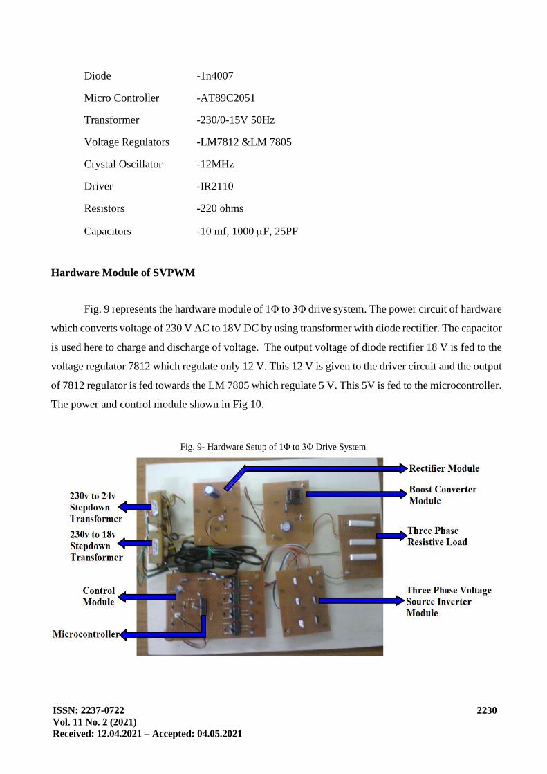
Hardware Module of SVPWM
Fig. 9 represents the hardware module of 1Φ to 3Φ drive system. The power circuit of hardware
which converts voltage of 230 V AC to 18V DC by using transformer with diode rectifier. The capacitor
is used here to charge and discharge of voltage. The output voltage of diode rectifier 18 V is fed to the
voltage regulator 7812 which regulate only 12 V. This 12 V is given to the driver circuit and the output
of 7812 regulator is fed towards the LM 7805 which regulate 5 V. This 5V is fed to the microcontroller.
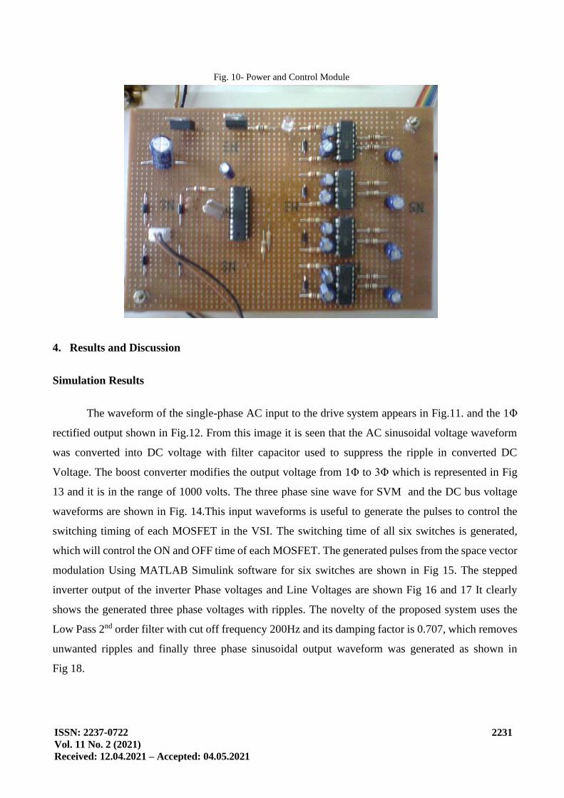
The power and control module shown in Fig 10.
Fig. 9- Hardware Setup of 1Φ to 3Φ Drive System
ISSN: 2237-0722
Vol. 11 No. 2 (2021)
Received: 12.04.2021 – Accepted: 04.05.2021
2231
Fig. 10- Power and Control Module
4. Results and Discussion
Simulation Results
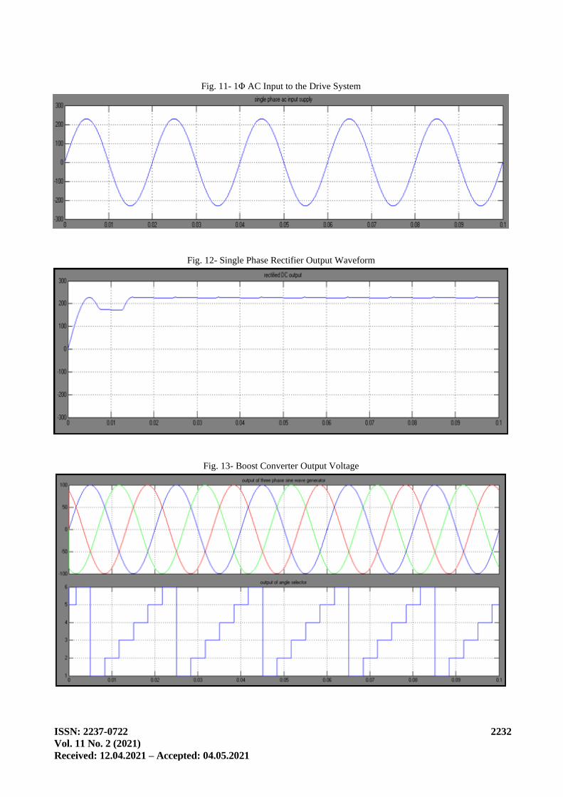
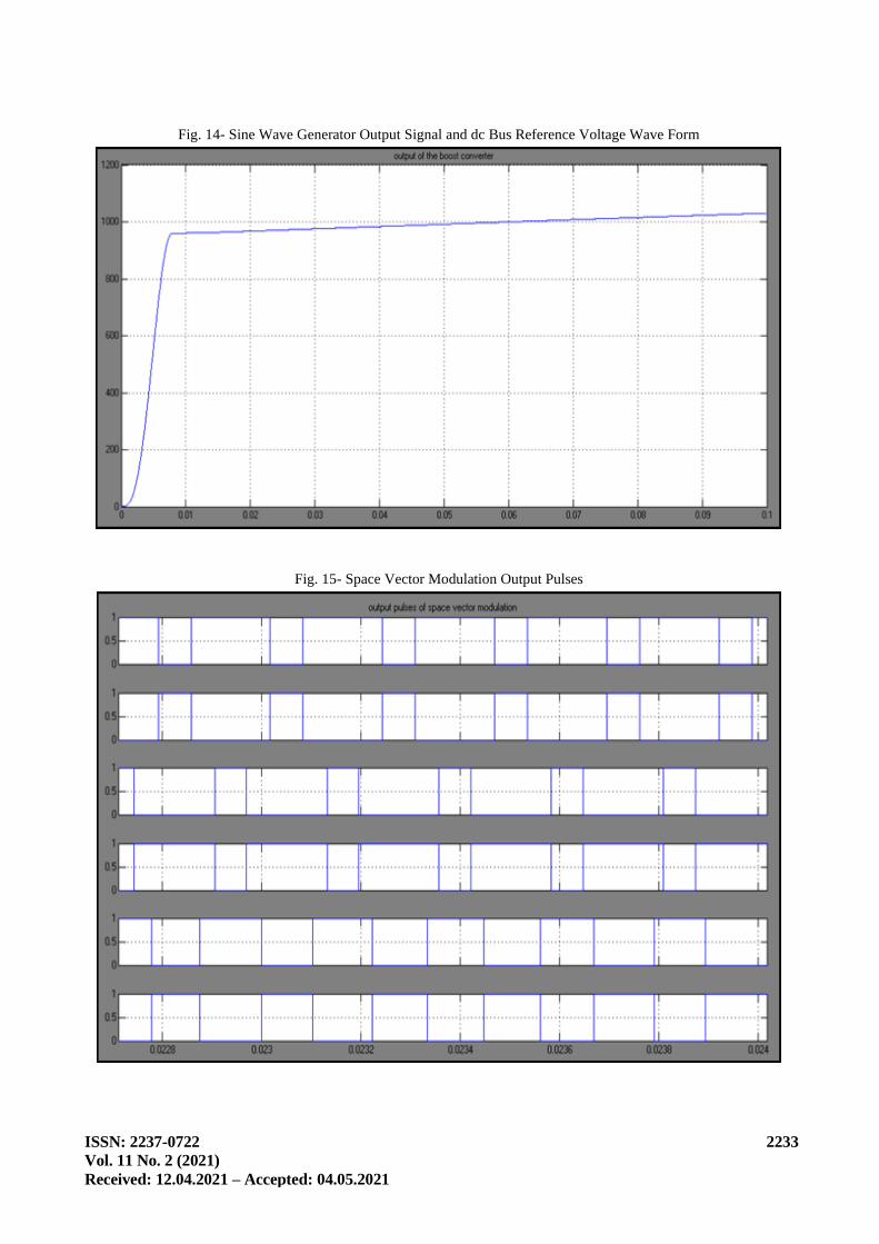
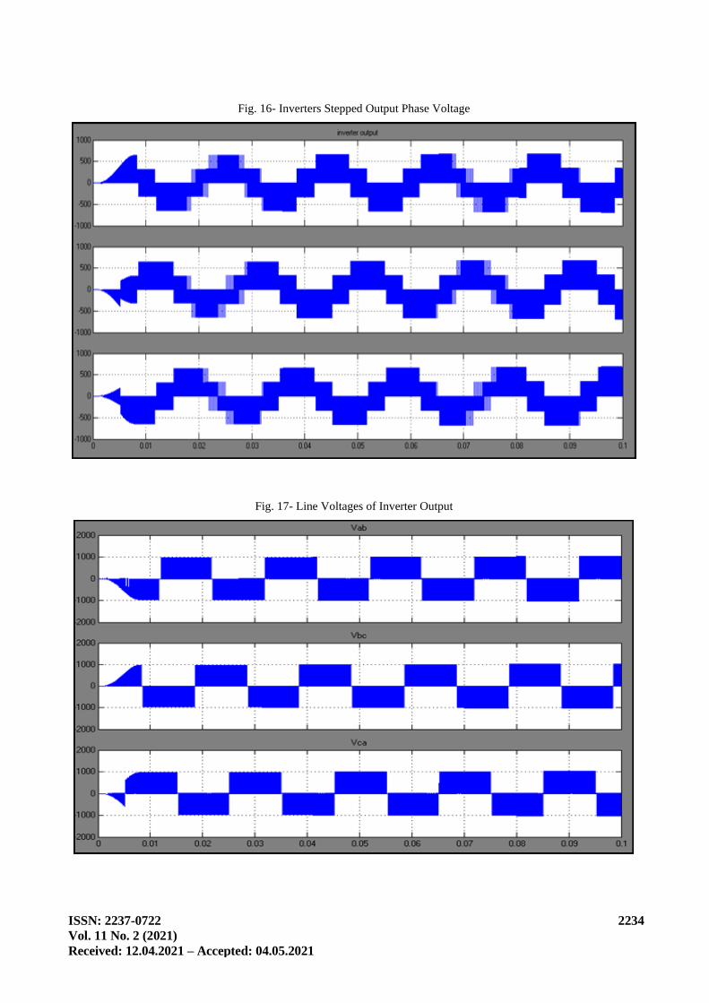
The waveform of the single-phase AC input to the drive system appears in Fig.11. and the 1Φ
rectified output shown in Fig.12. From this image it is seen that the AC sinusoidal voltage waveform
was converted into DC voltage with filter capacitor used to suppress the ripple in converted DC
Voltage. The boost converter modifies the output voltage from 1Φ to 3Φ which is represented in Fig
13 and it is in the range of 1000 volts. The three phase sine wave for SVM and the DC bus voltage
waveforms are shown in Fig. 14.This input waveforms is useful to generate the pulses to control the
switching timing of each MOSFET in the VSI. The switching time of all six switches is generated,
which will control the ON and OFF time of each MOSFET. The generated pulses from the space vector
modulation Using MATLAB Simulink software for six switches are shown in Fig 15. The stepped
inverter output of the inverter Phase voltages and Line Voltages are shown Fig 16 and 17 It clearly
shows the generated three phase voltages with ripples. The novelty of the proposed system uses the
Low Pass 2nd order filter with cut off frequency 200Hz and its damping factor is 0.707, which removes
unwanted ripples and finally three phase sinusoidal output waveform was generated as shown in
Fig 18.
ISSN: 2237-0722
Vol. 11 No. 2 (2021)
Received: 12.04.2021 – Accepted: 04.05.2021
2232
Fig. 11- 1Φ AC Input to the Drive System
Fig. 12- Single Phase Rectifier Output Waveform
Fig. 13- Boost Converter Output Voltage
ISSN: 2237-0722
Vol. 11 No. 2 (2021)
Received: 12.04.2021 – Accepted: 04.05.2021
2233
Fig. 14- Sine Wave Generator Output Signal and dc Bus Reference Voltage Wave Form
Fig. 15- Space Vector Modulation Output Pulses
ISSN: 2237-0722
Vol. 11 No. 2 (2021)
Received: 12.04.2021 – Accepted: 04.05.2021
2234
Fig. 16- Inverters Stepped Output Phase Voltage
Fig. 17- Line Voltages of Inverter Output

ISSN: 2237-0722
Vol. 11 No. 2 (2021)
Received: 12.04.2021 – Accepted: 04.05.2021
2235
Fig. 18- Three Phase Sinusoidal Output
Hardware Design Result
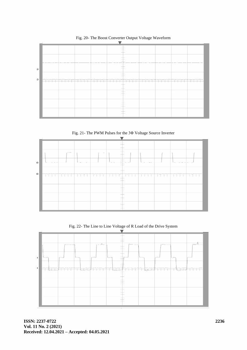
Hardware with help of proposed system circuit and description shows the 1Φ input AC voltage
converted into 3Φ AC voltage by using Space vector PWM technique. The Designed hardware clearly
shows that conversion of AC Voltage to DC voltage was done and pure DC voltage was observed from
the rectifier as shown in Fig. 19. The booster circuit increases the DC voltage for the required level of
inverter voltage as shown in Fig. 20. The timing of the pulses was generated by SVPWM method, and
the time duration was achieved by using Microcontroller AT89C2051. The generated pulses for the
MOSFET are shown in Fig. 21. Finally the three phase AC Voltage generated from the Designed
hardware has been supplied to the three phase induction motor. The performance of the induction motor
was found to be smooth due to reduced total harmonic distortion. The converted three phase line volage
shown in fig. 22.
Fig. 19- The Rectifier Output Waveform
ISSN: 2237-0722
Vol. 11 No. 2 (2021)
Received: 12.04.2021 – Accepted: 04.05.2021
2236
Fig. 20- The Boost Converter Output Voltage Waveform
Fig. 21- The PWM Pulses for the 3Φ Voltage Source Inverter
Fig. 22- The Line to Line Voltage of R Load of the Drive System
ISSN: 2237-0722
Vol. 11 No. 2 (2021)
Received: 12.04.2021 – Accepted: 04.05.2021
2237
5. Conclusion
A 1Φ to 3Φ drive system consists of 1Φ bridge rectifier, a 3Φ inverter and an asynchronous
motor which shows various control strategies, its system models and also it includes the space vector
technique were developed. The correlation of the standard and proposed configurations has been
analyzed. In contrast to the typical topology, the developed system allows to minimize the rectifier
switch currents. In order to improve the fault tolerance characteristics, the THD (Total Harmonics
Distortion) plays a vital role. This distortion factor is achieved by maintaining the similar switching
frequency and grid current. Furthermore, the system developed in the present study has advantages
such as reduced cost and losses due to fewer components over the traditional system. Compared to
reviewed systems this proposed system incurs less investment cost and it is highly advantageous. The
software and hardware output of the system was controlled precisely, even though the system exhibits
the dynamic errors.
References
Yoshiya Ohmma and Jun-ichi Itoh (2010), ‘Space Vector Modulation for a Single Phase to Three Phase
Converter Using and Active Buffer’, IEEE Trans on Industrial electronics, Iran.
Ricardo Quadros Machado and Simone Buso (2006), ‘A Line-interactive single phase to three phase
converter system’, IEEE transactions on industry applications, India.
Radha Krishna and Amar Kiran (2012), ‘Modeling of Single-Phase to Three-Phase Drive System Using
Two Parallel Single-Phase Rectifiers’, International Journal of Modern Engineering Research
(IJMER), 2(5), 3899-3907
Cursino Brandao Jacobina and Edison Roberto Cabral da Silva (2008). Reduced Switch Count Multiple
Three-Phase Ac Machine Drive Systems’. 2nd International Conference on Power Electronics and
Intelligent Transportation System.
D.C. Lee and Y.S. Kim, ‘Control of single-phase-to-three-phase AC/DC/AC PWM converters for
induction motor drives’, IEEE Trans. Ind. Electron., vol. 54, no. 2, pp. 797–804, Apr. 2007.
L. Woo-Cheol, L. Taeck-Kie, and H. Dong-Seok, ‘A three phase parallel active power filter operating
with PCC voltage compensation with consideration for an unbalanced load’, IEEE Trans. Power
Electron., vol. 17, no. 5, pp. 807–814, Sep. 2002.
L. Asiminoaei, E. Aeloiza, P.N. Enjeti, F. Blaabjerg, and G. Danfoss, ‘Shunt active-power-filter
topology based on parallel interleaved inverters’, IEEE Trans. Ind. Electron., 55(3), 1175–1189, Mar.
2008.
M. Ashari, W.L. Keerthipala, and C.V. Nayar, ‘A single phase parallel connected uninterruptible power
supply/demand side management system’, IEEE Trans. Energy Convers., 15(1), 97–102, 2000.
J.K. Park, J.M. Kwon, E.H. Kim, and B.H. Kwon, ‘High-performance transformer less online UPS’,
IEEE Trans. Ind. Electron., vol. 55, no. 8, pp. 2943–2953, Aug. 2008.

ISSN: 2237-0722
Vol. 11 No. 2 (2021)
Received: 12.04.2021 – Accepted: 04.05.2021
2238
Z. Ye, D. Boroyevich, J.Y. Choi, and F.C. Lee, ‘Control of circulating current in two parallel
three-phase boost rectifiers’, IEEE Trans. Power Electron., vol. 17, no. 5, pp. 609–615, Sep. 2002.
S.K. Mazumder, ‘Continuous and discrete variable-structure controls for parallel three-phase boost
rectifier’, IEEE Trans. Ind. Electron., vol. 52, no. 2, pp. 340–354, Apr. 2005.
Z. Ye, P. Jain, and P. Sen, ‘Circulating current minimization in high frequency AC power distribution
architecture with multiple inverter modules operated in parallel’, IEEE Trans. Ind. Electron., vol. 54,
no. 5, pp. 2673–2687, Oct. 2007.
Ganesh Babu Loganathan, Praveen M., Jamuna Rani D., “Intelligent classification technique for breast
cancer classification using digital image processing approach” IEEE Xplore Digital Library 2019,
Pp.1-6.
M. Viswanathan, Ganesh Babu Loganathan, and S. Srinivasan, “IKP based biometric authentication
using artificial neural network”, AIP Conference Proceedings (2020), Volume 2271, Issue 1, 030030.
Mohammed Abdulghani Taha and Ganesh Babu Loganathan, “Hybrid algorithms for spectral noise
removal in hyper spectral images” AIP Conference Proceedings (2020), Volume 2271, Issue 1,
pp 030013.
Dr. Idris Hadi Salih, Ganesh Babu Loganathan, “Induction motor fault monitoring and fault
classification using deep learning probablistic neural network” Solid State Technology (2020),
Volume 63, Issue 6, PP No. 2196-2213.
Ganesh Babu Loganathan “Design and analysis of high gain Re Boost-Luo converter for high power
DC application”, Materials Today: Proceedings (2020), Volume 33, Part 1, PP 13-22.
Ganesh Babu Loganathan, Dr.E. Mohan, R. Siva Kumar, “Iot Based Water and Soil Quality Monitoring
System”, International Journal of Mechanical Engineering and Technology (IJMET) (2019), Vol.10
Issue No.2, P. 537-541.
Suganthi K, Idris Hadi Salih, Ganesh Babu Loganathan, and Sundararaman K, “A Single Switch
Bipolar Triple Output Converter with Fuzzy Control”, International Journal of Advanced Science and
Technology, (2020), Vol. 29, No. 5, (2020), P. 2386 – 2400.
Ganesh Babu Loganathan, “Can Based Automated Vehicle Security System”, International Journal of
Mechanical Engineering and Technology (IJMET) (2019), Vol.10 Issue No.07, 46-51.
B.K. Patle, Ganesh Babu L, Anish Pandey, D.R.K. Parhi, A. Jagadeesh, A review: On path planning
strategies for navigation of mobile robot, Defence Technology, 15, Issue 4, August 2019, 582-606.
A. Senthil Kumar, Dr. Venmathi AR, L. Ganesh Babu, G. Suresh, “Smart Agriculture Robo With Leaf
Diseases Detection Using IOT”, European Journal of Molecular & Clinical Medicine, 07(09),
2462-2469.
Ganesh Babu L 2019 Influence of benzoyl chloride treatment on the tribological characteristics of
Cyperus pangorei fibers based nonasbestos brake friction composites Mater. Res. Express 7 015303.
Manoharan S, Sai Krishnan G, Babu L G, Vijay R and Singaravelu D L 2019 Synergistic effect of red
mud-iron sulfide particles on fade recovery characteristics of non-asbestos organic brake friction
composites Mater. Res. Express 6 105311.
Manoharan S, Shihab A I, Alemdar A S A, Ganesh Babu L, Vijay R and Lenin Singaravelu D 2019
Influence of recycled basalt-aramid fibres integration on the mechanical and thermal properties of
brake friction composites Material Research Express 6 115310.
ISSN: 2237-0722
Vol. 11 No. 2 (2021)
Received: 12.04.2021 – Accepted: 04.05.2021
2239
Qaysar S. Mahdi, “Prediction of Mobile Radio Wave Propagation in Complex Topography”, Eurasian
Journal of Science & Engineering, Volume 4, Issue 1 (Special Issue); September, 2018, 49-55.
Qaysar S. Mahd, “Survivability Analysis of GSM Network Systems”, Eurasian Journal of Science &
Engineering, Volume 3, Issue 3; June, 2018, 113-123.
Qaysar S. Mahdi, “Comparison Study of Multi-Beams Radar under Different Radar Cross Section and
Different Transmitting Frequency”, Eurasian Journal of Science & Engineering, Volume 3, Issue 3;
June, 2018, 1-11.
Qaysar Salih Mahdi, Idris Hadi Saleh, Ghani Hashim, Ganesh Babu Loganathan, “Evaluation of Robot
Professor Technology in Teaching and Business”, Information Technology in Industry, Volume 09,
Issue 01, 1182-1194.
Ellappan Mohan, Arunachalam Rajesh, Gurram Sunitha, Reddy Madhavi Konduru, Janagaraj
Avanija, Loganathan Ganesh Babu, “A deep neural network learning‐based speckle noise removal
technique for enhancing the quality of synthetic‐aperture radar images”, Concurrency and
Computation-Practice & Experience, https://doi.org/10.1002/cpe.6239.
Ganesh Babu Loganathan, Idris Hadi Salih, A. Karthikayen, N. Satheesh Kumar, Udayakumar
Durairaj. (2021). EERP: Intelligent Cluster based Energy Enhanced Routing Protocol Design over
Wireless Sensor Network Environment. International Journal of Modern Agriculture, 10(2),
1725 - 1736. http://www.modern-journals.com/index.php/ijma/article/view/908
C. Kannan, Nalin Kant Mohanty, R. Selvarasu, “A new topology for cascaded H-bridge multilevel
inverter with PI and Fuzzy control”, Energy Procedia, 117, 2017, 917-926.
https://doi.org/10.1016/j.egypro.2017.05.211.
C. Kannan, and C.K. Kishore, “A Comparison of Three Phase 27 Level Inverter Scheme under No
Load and Multiple Load Conditions”, Bulletin of Electrical Engineering and Informatics Vol. 3, No.4,
245-250, December 2014
Nandagopal, V., Maheswari, V. and Kannan, C. (2016) Newly Constructed Real Time ECG
Monitoring System Using LabView. Circuits and Systems, 7, 4227-4235.
Babu Loganathan, Ganesh; E. Mohan, Dr. High Quality Intelligent Database Driven Microcontroller
Based Heartbeat Monitoring System. International Journal of Engineering & Technology, [S.l.], v. 7,
n. 4.6, p. 472-476, 2018.
Loganathan, Ganesh Babu, Vanet Based Secured Accident Prevention System (September 10, 2019).
International Journal of Mechanical Engineering and Technology, 10(6), 2019, pp. 285-291,
Manikandan Ganesan, Ishwarya K.R, Demoz Lisanework, Ayenachew Hailu Mengiste. (2021).
Investigation on autonomous pesticide spraying robotic vehicle in agriculture field. International
Journal of Modern Agriculture, 10(1), 382-386.
A. Senthil Kumar, G. Suresh, S. Lekashri, L. Ganesh Babu, R. Manikandan, “Smart Agriculture System
with E – Carbage Using Iot”. International Journal of Modern Agriculture, 10(1), 2021 928-931.
S Priyadharsini, TS Sivakumaran, C Kannan, “Performance analysis of photovoltaic-based SL-quasi Z
source inverter”. International Journal of Energy Technology and Policy, 1(3), 254-264.
Maheswari, V., Nandagopal, V. and Kannan, C. (2016), “Performance Metric of Z Source CHB
Multilevel Inverter FED IM for Selective Harmonic Elimination and THD Reduction”, Circuits and
Systems, 7, 3794-3806. doi: 10.4236/cs.2016.711317