Embed Size (px)
Citation preview
Design and Implementation of a BroadbandRF-DAC Transmitter for Wireless
Communications
Von der Fakultät für Elektrotechnik und Informationstechnikder Rheinisch-Westfälischen Technischen Hochschule Aachenzur Erlangung des akademischen Grades eines Doktors der
Ingenieurwissenschaften genehmigte Dissertation
vorgelegt von
Diplom-Ingenieur
Niklas Zimmermann
aus Münster
Berichter: Universitätsprofessor Dr.-Ing. Stefan HeinenUniversitätsprofessor Dr.-Ing.Gerd Ascheid
Tag der mündlichen Prüfung: 1. Juli 2011
Diese Dissertation ist auf den Internetseiten der Hochschulbibliothek online verfügbar.
Bibliografische Information der Deutschen NationalbibliothekDie Deutsche Nationalbibliothek verzeichnet diese Publikation in der Deutschen Nationalbibliografie; detaillierte bibliografische Daten sind im Internet überhttp://dnb.d-nb.de abrufbar.
ISBN 978-3-8439-0042-3
D 82 (Diss. RWTH Aachen University, 2011)
© Verlag Dr. Hut, München 2011Sternstr. 18, 80538 MünchenTel.: 089/66060798www.dr.hut-verlag.de
Die Informationen in diesem Buch wurden mit großer Sorgfalt erarbeitet. Dennoch können Fehler nicht vollständig ausgeschlossen werden. Verlag, Autoren und ggf. Übersetzer übernehmen keine juristische Verantwortung oder irgendeine Haftung für eventuell verbliebene fehlerhafte Angaben und deren Folgen.
Alle Rechte, auch die des auszugsweisen Nachdrucks, der Vervielfältigung und Verbreitung in besonderen Verfahren wie fotomechanischer Nachdruck, Fotokopie, Mikrokopie, elektronische Datenaufzeichnung einschließlich Speicherung und Übertragung auf weitere Datenträger sowie Übersetzung in andere Sprachen, behält sich der Autor vor.
1. Auflage 2011

To the memory of my father, Gebhard Zimmermann


Acknowledgment
First of all, I want to thank Prof. Dr.-Ing. Stefan Heinen. This thesis would nothave been possible without him, as he gave me the opportunity to work on thisexciting topic and shared his rich experience in the field of RF and analog circuitand system design with me.I would like to thank all colleagues and students at IAS – especially my
officemates Tobias Werth, Stephan Bannwarth, and Stefan Dietrich – for thegreat atmosphere, which always made me enjoy my time here.A big thank you goes to all the people that contributed to the successful
implementation of the RF-DAC transmitter prototype chip:• Bastian Mohr, who implemented serial data interface and mismatch shaper
and also took care of lots of other tasks.• Björn Thiel, who implemented most of the high-speed digital circuits.• Yifan Wang, without his experience in functional verification and his great
commitment, this project would not have succeeded.• Jan Henning Müller, for implementing the configuration interface and
supporting the toplevel synthesis of the digital blocks.• Dirk Bormann, for the great EDA tool support.• René Adams, for the help with the measurement setup.• Tobias Werth, Stefan Kählert and Ahmed Farouk Aref for lots of very
fruitful discussions.Furthermore, I would like to acknowledge the support of Prof. Brüning’s Com-puter Architecture Group at University of Heidelberg, who helped a lot with theimplementation of the digital building blocks and the used EDA tools.
I want to thank Dr.-Ing. Ralf Wunderlich for lots of guidance and good advice,especially during my first months at IAS.I am grateful to all the colleagues that worked on the CoSiC PA project at
the former Infineon Technologies design center in Kista, Sweden, and especiallyto Dr. Ted Johansson, from whom I learned a lot about RF circuit design as wellas project management.Last but not least, I would like to thank my family for their encouragement
and support during my studies. Particularly, I want to thank Frauke for herpatience and understanding during my busy times of working on this thesis.

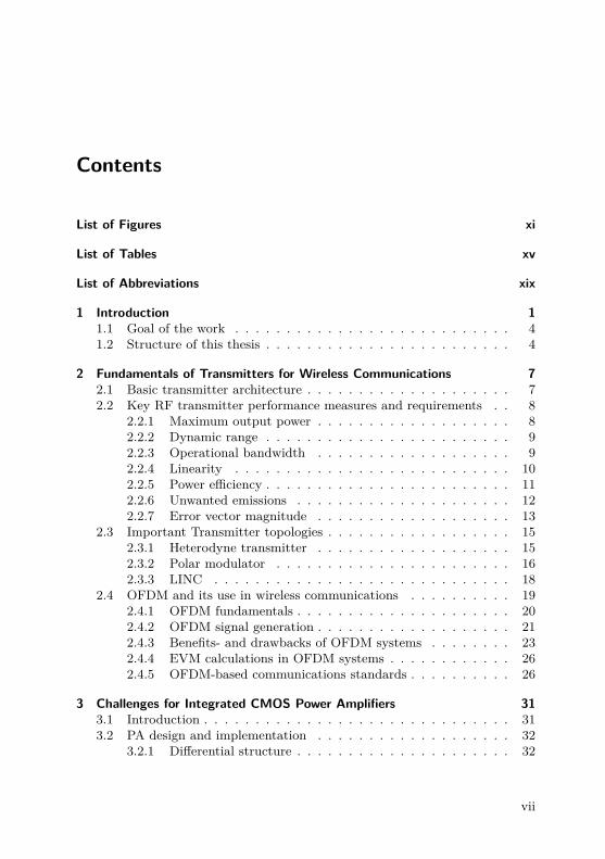
Contents
List of Figures xi
List of Tables xv
List of Abbreviations xix
1 Introduction 11.1 Goal of the work . . . . . . . . . . . . . . . . . . . . . . . . . . . 41.2 Structure of this thesis . . . . . . . . . . . . . . . . . . . . . . . . 4
2 Fundamentals of Transmitters for Wireless Communications 72.1 Basic transmitter architecture . . . . . . . . . . . . . . . . . . . . 72.2 Key RF transmitter performance measures and requirements . . 8
2.2.1 Maximum output power . . . . . . . . . . . . . . . . . . . 82.2.2 Dynamic range . . . . . . . . . . . . . . . . . . . . . . . . 92.2.3 Operational bandwidth . . . . . . . . . . . . . . . . . . . 92.2.4 Linearity . . . . . . . . . . . . . . . . . . . . . . . . . . . 102.2.5 Power efficiency . . . . . . . . . . . . . . . . . . . . . . . . 112.2.6 Unwanted emissions . . . . . . . . . . . . . . . . . . . . . 122.2.7 Error vector magnitude . . . . . . . . . . . . . . . . . . . 13
2.3 Important Transmitter topologies . . . . . . . . . . . . . . . . . . 152.3.1 Heterodyne transmitter . . . . . . . . . . . . . . . . . . . 152.3.2 Polar modulator . . . . . . . . . . . . . . . . . . . . . . . 162.3.3 LINC . . . . . . . . . . . . . . . . . . . . . . . . . . . . . 18
2.4 OFDM and its use in wireless communications . . . . . . . . . . 192.4.1 OFDM fundamentals . . . . . . . . . . . . . . . . . . . . . 202.4.2 OFDM signal generation . . . . . . . . . . . . . . . . . . . 212.4.3 Benefits- and drawbacks of OFDM systems . . . . . . . . 232.4.4 EVM calculations in OFDM systems . . . . . . . . . . . . 262.4.5 OFDM-based communications standards . . . . . . . . . . 26
3 Challenges for Integrated CMOS Power Amplifiers 313.1 Introduction . . . . . . . . . . . . . . . . . . . . . . . . . . . . . . 313.2 PA design and implementation . . . . . . . . . . . . . . . . . . . 32
3.2.1 Differential structure . . . . . . . . . . . . . . . . . . . . . 32
vii
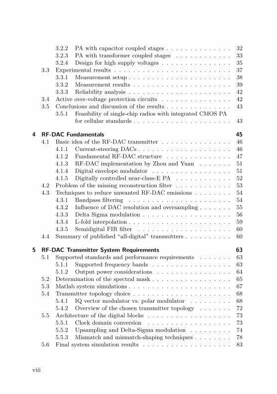
3.2.2 PA with capacitor coupled stages . . . . . . . . . . . . . . 323.2.3 PA with transformer coupled stages . . . . . . . . . . . . 333.2.4 Design for high supply voltages . . . . . . . . . . . . . . . 35
3.3 Experimental results . . . . . . . . . . . . . . . . . . . . . . . . . 373.3.1 Measurement setup . . . . . . . . . . . . . . . . . . . . . . 383.3.2 Measurement results . . . . . . . . . . . . . . . . . . . . . 393.3.3 Reliability analysis . . . . . . . . . . . . . . . . . . . . . . 42
3.4 Active over-voltage protection circuits . . . . . . . . . . . . . . . 423.5 Conclusions and discussion of the results . . . . . . . . . . . . . . 43
3.5.1 Feasibility of single-chip radios with integrated CMOS PAfor cellular standards . . . . . . . . . . . . . . . . . . . . . 43
4 RF-DAC Fundamentals 454.1 Basic idea of the RF-DAC transmitter . . . . . . . . . . . . . . . 46
4.1.1 Current-steering DACs . . . . . . . . . . . . . . . . . . . . 464.1.2 Fundamental RF-DAC structure . . . . . . . . . . . . . . 474.1.3 RF-DAC implementation by Zhou and Yuan . . . . . . . 514.1.4 Digital envelope modulator . . . . . . . . . . . . . . . . . 514.1.5 Digitally controlled near-class-E PA . . . . . . . . . . . . 52
4.2 Problem of the missing reconstruction filter . . . . . . . . . . . . 534.3 Techniques to reduce unwanted RF-DAC emissions . . . . . . . . 54
4.3.1 Bandpass filtering . . . . . . . . . . . . . . . . . . . . . . 544.3.2 Influence of DAC resolution and oversampling . . . . . . . 554.3.3 Delta Sigma modulation . . . . . . . . . . . . . . . . . . . 564.3.4 L-fold interpolation . . . . . . . . . . . . . . . . . . . . . . 594.3.5 Semidigital FIR filter . . . . . . . . . . . . . . . . . . . . 60
4.4 Summary of published “all-digital” transmitters . . . . . . . . . . 60
5 RF-DAC Transmitter System Requirements 635.1 Supported standards and performance requirements . . . . . . . 63
5.1.1 Supported frequency bands . . . . . . . . . . . . . . . . . 635.1.2 Output power considerations . . . . . . . . . . . . . . . . 64
5.2 Determination of the spectral mask . . . . . . . . . . . . . . . . . 655.3 Matlab system simulations . . . . . . . . . . . . . . . . . . . . . . 675.4 Transmitter topology choice . . . . . . . . . . . . . . . . . . . . . 68
5.4.1 IQ vector modulator vs. polar modulator . . . . . . . . . 685.4.2 Overview of the chosen transmitter topology . . . . . . . 72
5.5 Architecture of the digital blocks . . . . . . . . . . . . . . . . . . 735.5.1 Clock domain conversion . . . . . . . . . . . . . . . . . . 735.5.2 Upsampling and Delta-Sigma modulation . . . . . . . . . 745.5.3 Mismatch and mismatch-shaping techniques . . . . . . . . 78
5.6 Final system simulation results . . . . . . . . . . . . . . . . . . . 83
viii
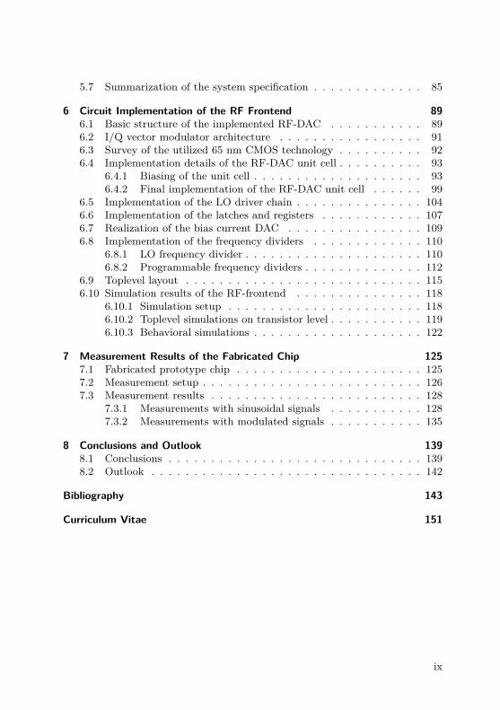
5.7 Summarization of the system specification . . . . . . . . . . . . . 85
6 Circuit Implementation of the RF Frontend 896.1 Basic structure of the implemented RF-DAC . . . . . . . . . . . 896.2 I/Q vector modulator architecture . . . . . . . . . . . . . . . . . 916.3 Survey of the utilized 65 nm CMOS technology . . . . . . . . . . 926.4 Implementation details of the RF-DAC unit cell . . . . . . . . . . 93
6.4.1 Biasing of the unit cell . . . . . . . . . . . . . . . . . . . . 936.4.2 Final implementation of the RF-DAC unit cell . . . . . . 99
6.5 Implementation of the LO driver chain . . . . . . . . . . . . . . . 1046.6 Implementation of the latches and registers . . . . . . . . . . . . 1076.7 Realization of the bias current DAC . . . . . . . . . . . . . . . . 1096.8 Implementation of the frequency dividers . . . . . . . . . . . . . 110
6.8.1 LO frequency divider . . . . . . . . . . . . . . . . . . . . . 1106.8.2 Programmable frequency dividers . . . . . . . . . . . . . . 112
6.9 Toplevel layout . . . . . . . . . . . . . . . . . . . . . . . . . . . . 1156.10 Simulation results of the RF-frontend . . . . . . . . . . . . . . . 118
6.10.1 Simulation setup . . . . . . . . . . . . . . . . . . . . . . . 1186.10.2 Toplevel simulations on transistor level . . . . . . . . . . . 1196.10.3 Behavioral simulations . . . . . . . . . . . . . . . . . . . . 122
7 Measurement Results of the Fabricated Chip 1257.1 Fabricated prototype chip . . . . . . . . . . . . . . . . . . . . . . 1257.2 Measurement setup . . . . . . . . . . . . . . . . . . . . . . . . . . 1267.3 Measurement results . . . . . . . . . . . . . . . . . . . . . . . . . 128
7.3.1 Measurements with sinusoidal signals . . . . . . . . . . . 1287.3.2 Measurements with modulated signals . . . . . . . . . . . 135
8 Conclusions and Outlook 1398.1 Conclusions . . . . . . . . . . . . . . . . . . . . . . . . . . . . . . 1398.2 Outlook . . . . . . . . . . . . . . . . . . . . . . . . . . . . . . . . 142
Bibliography 143
Curriculum Vitae 151
ix

x
List of Figures
1.1 Classical analog transmitter. . . . . . . . . . . . . . . . . . . . . 21.2 “Digital RF” reconfigurable transmitters. . . . . . . . . . . . . . 3
2.1 Block diagram of a conventional analog quadrature RF transmit-ter. . . . . . . . . . . . . . . . . . . . . . . . . . . . . . . . . . . 7
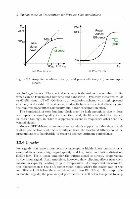
2.2 Amplifier nonlinearities (a) and power efficiency (b) versus inputpower. . . . . . . . . . . . . . . . . . . . . . . . . . . . . . . . . . 10
2.3 IMD and DAC noise dominate at different frequency regions. . . 132.4 Measuring the EVM in a constellation diagram. . . . . . . . . . 142.5 Block diagram of a two-step heterodyne transmitter. . . . . . . 152.6 Block diagram of a polar transmitter. . . . . . . . . . . . . . . . 172.7 Simplified block diagram of a LINC transmitter and outphasing
principle. . . . . . . . . . . . . . . . . . . . . . . . . . . . . . . . 182.8 Basic principle of multiple subcarrier signal generation. . . . . . 202.9 Single carrier signal vs. OFDM signal. . . . . . . . . . . . . . . . 212.10 Using the inverse FFT to generate OFDM signals. . . . . . . . . 222.11 Adding a cyclic prefix to an OFDM signal. . . . . . . . . . . . . . 232.12 Spectrum of a WLAN 802.11a/g/n baseband signal. . . . . . . . 242.13 Maximum theoretical PAPR vs. number of OFDM subcarriers N . 252.14 SC-FDMA baseband encoding. . . . . . . . . . . . . . . . . . . . 262.15 PAPR curves of OFDM and DTFS-OFDM. . . . . . . . . . . . . 27
3.1 PA with capacitor coupled stages. . . . . . . . . . . . . . . . . . . 333.2 PA with transformer coupled stages. . . . . . . . . . . . . . . . . 343.3 An equivalent circuit for the transformers. . . . . . . . . . . . . . 353.4 Layout of the double gate transistor. . . . . . . . . . . . . . . . . 363.5 Chip photos of the two power amplifiers. . . . . . . . . . . . . . . 383.6 Lattice-type LC-balun. . . . . . . . . . . . . . . . . . . . . . . . . 393.7 Pout and PAE vs. Pin of PA with transformers. . . . . . . . . . . 403.8 Pout and PAE vs. frequency of PA with transformers. . . . . . . 403.9 Pout and PAE vs. Pin of PA with LC coupled stages. . . . . . . . 413.10 Pout and PAE vs. frequency of PA with LC coupled stages. . . . 41
4.1 Principle of a current steering DAC. . . . . . . . . . . . . . . . . 47
xi
4.2 One unit element of a the RF-DAC implementation by Luschaset al. . . . . . . . . . . . . . . . . . . . . . . . . . . . . . . . . . 48
4.3 One unit element of a the double balanced RF-DAC implementa-tion by Eloranta et al. . . . . . . . . . . . . . . . . . . . . . . . . 49
4.4 Block diagram of a direct-digital I/Q modulator utilizing RF-DACs. . . . . . . . . . . . . . . . . . . . . . . . . . . . . . . . . 50
4.5 RF-DAC architecture by Zhou and Yuan. . . . . . . . . . . . . . 514.6 Digital envelope modulator DAC. . . . . . . . . . . . . . . . . . . 524.7 Near-class-E DPA. . . . . . . . . . . . . . . . . . . . . . . . . . . 534.8 Filtering of the DAC signal replica. . . . . . . . . . . . . . . . . . 544.9 Block diagram of a single-bit ∆Σ DAC. . . . . . . . . . . . . . . 564.10 ∆ΣM NTF over normalized frequency in dependence of the mod-
ulator order. . . . . . . . . . . . . . . . . . . . . . . . . . . . . . 584.11 Principle of L-fold interpolation. . . . . . . . . . . . . . . . . . . 59
5.1 Scenario of two parallel running closeby radios. . . . . . . . . . . 655.2 Polar modulator comprising RF-DAC and all-digital PLL. . . . . 685.3 Principle of the quadrature signal generation in a Cartesian vs.
polar methodology. . . . . . . . . . . . . . . . . . . . . . . . . . . 695.4 WLAN OFDM signal decomposed into magnitude and phase parts. 705.5 Output signal of the polar modulator with limited PLL tuning
range. . . . . . . . . . . . . . . . . . . . . . . . . . . . . . . . . . 715.6 Simplified block diagram of the proposed I/Q RF-DAC transmitter. 725.7 Implementation of one interpolation filter stage. . . . . . . . . . 755.8 Frequency response of one interpolation filter stage. . . . . . . . 755.9 ∆Σ shaped spectrum of a 20MHz wide OFDM signal. . . . . . . 765.10 Spectrum of a 1st order ∆Σ shaped 20MHz wide OFDM signal
for different converter resolutions. . . . . . . . . . . . . . . . . . 775.11 3rd order ∆Σ modulated spectrum with additional notches in the
noise transfer function. . . . . . . . . . . . . . . . . . . . . . . . 785.12 Simple model of static and dynamic mismatch errors. . . . . . . 795.13 Block diagrams of tree shaper and DWA. . . . . . . . . . . . . . 805.14 Block diagram of the mismatch-shaping ESL and segmented DAC
architecture. . . . . . . . . . . . . . . . . . . . . . . . . . . . . . 815.15 Effect of mismatch and mismatch shaping techniques on the
OFDM output spectrum. . . . . . . . . . . . . . . . . . . . . . . 825.16 Spectrum and emission mask of a 2.5GHz LTE signal, simulated
with Matlab . . . . . . . . . . . . . . . . . . . . . . . . . . . . . . 845.17 Simulated constellation plot of one 16QAM modulated OFDM
subcarrier. . . . . . . . . . . . . . . . . . . . . . . . . . . . . . . 855.18 Detailed block diagram of the RF-DAC based transmitter prototype. 87
xii
6.1 Principle implementation of the RF-DAC. . . . . . . . . . . . . . 906.2 Block diagram of the RF-DAC based I/Q vector modulator. . . . 916.3 NMOS I-V device characteristics for a 60 nm gatelength transistor
with an aspect ratio of 100. . . . . . . . . . . . . . . . . . . . . . 926.4 Cascode current mirror and its small signal equivalent circuit to
determine rout. . . . . . . . . . . . . . . . . . . . . . . . . . . . . 946.5 High swing Sooch cascode current mirror. . . . . . . . . . . . . . 966.6 Sooch cascode current mirror with two input branches. . . . . . 986.7 Circuit implementation of RF-DAC unit cell and biasing. . . . . 996.8 Implementation of the data switches with transmission gates. . . 1006.9 Output impedance vs. frequency of a Sooch cascode current mirror
for different gate lengths. . . . . . . . . . . . . . . . . . . . . . . 1016.10 Layout of one MSB RF-DAC unit cell. . . . . . . . . . . . . . . . 1026.11 Common-centroid layout of the LSB unit cells. . . . . . . . . . . 1026.12 Sinusoidal output current waveform of one 9 bit RF-DAC. . . . . 1046.13 Single-ended block diagram of LO driver with control logic. . . . 1056.14 Output voltage waveform of the LO driver with control logic. . . 1066.15 Schematic of the latch driving the RF-DAC unit cell. . . . . . . 1086.16 Schematic of the programmable bias current DAC. . . . . . . . . 1096.17 Block diagram of the 0°/90° LO frequency divider. . . . . . . . 1106.18 Schematic of the self-biased LO input buffer. . . . . . . . . . . . 1116.19 Schematic of the latch for the LO frequency divider. . . . . . . . 1126.20 Realization of a multi-modulus frequency divider. . . . . . . . . . 1126.21 Overview of the programmable, LO derived clock generation. . . 1136.22 Programmable frequency divider. . . . . . . . . . . . . . . . . . . 1146.23 Schematic of a positive edge triggered TSPC register. . . . . . . 1146.24 Toplevel layout of the prototype chip. . . . . . . . . . . . . . . . 1156.25 Pinout of the QFN48 package. . . . . . . . . . . . . . . . . . . . 1166.26 Layout of the analog and mixed-signal circuits. . . . . . . . . . . 1176.27 Output spectrum of the transmitter for a 20MHz sinewave SSB
input, simulated on transistor level. . . . . . . . . . . . . . . . . . 1196.28 Simulated output power of SSB 20MHz sinewave, LO leakage,
image signal and DC power consumption vs. power control. . . 1206.29 Simulated output spectrum of a 20MHz OFDM WLAN signal. . 1216.30 Simulated output spectrum of the transmitter for a 20MHz wide
OFDM signal simulated with Verilog-AMS behavioral models. . 122
7.1 Chip photograph of the RF-DAC transmitter protoype. . . . . . 1257.2 Photo of the RF test PCB. . . . . . . . . . . . . . . . . . . . . . 1267.3 Structure of the measurement setup. . . . . . . . . . . . . . . . . 1277.4 Output spectrum of a 5MHz sinusoid. . . . . . . . . . . . . . . . 129
xiii

7.5 Output power of a 5MHz single-sideband sinusoid, image signaland LO feedthrough vs. baseband signal amplitude. . . . . . . . 130
7.6 Measured output power of a 5MHz single-sideband sinusoid, imagesignal and LO feedthrough vs. power control. . . . . . . . . . . . 133
7.7 Output spectrum of a 20MHz wide 64QAM OFDM signal at480MHz sampling rate. . . . . . . . . . . . . . . . . . . . . . . . 135
7.8 Wideband spectrum of the same 20MHz wide 64QAM OFDMsignal. . . . . . . . . . . . . . . . . . . . . . . . . . . . . . . . . 136
7.9 Output spectrum of a 40MHz wide “turbo-mode” WLAN signalat 500MHz sampling rate. . . . . . . . . . . . . . . . . . . . . . . 137
xiv
List of Tables
2.1 Overview of important OFDM-based wireless communicationstandards. . . . . . . . . . . . . . . . . . . . . . . . . . . . . . . 29
4.1 Performance summary of different direct-digital transmitters. . . 61
5.1 Summary of the RF-DAC based transmitter system specifications. 86
6.1 Transistor sizes in the LSB and MSB RF-DAC unit cells withbiasing. . . . . . . . . . . . . . . . . . . . . . . . . . . . . . . . . 100
6.2 Transistor width in the latches driving the LSB and MSB RF-DACunit cells. . . . . . . . . . . . . . . . . . . . . . . . . . . . . . . . 108
7.1 Power consumption of the analog and RF blocks at differentoutput amplitudes. . . . . . . . . . . . . . . . . . . . . . . . . . . 131
7.2 Power consumption of the analog and RF blocks for differentpower control settings. . . . . . . . . . . . . . . . . . . . . . . . . 132
xv

xvi

List of Abbreviations
3GPP 3rd Generation Partnership ProjectACPR adjacent channel power ratioADPLL all-digital PLLAM amplitude modulationASK amplitude shift keyingbalun balanced-to-unbalanced converterBER bit error rateBOM bill of materialsCCDF complementary cumulative distribution functionCDC clock domain converterCDMA code division multiple accessCIC cascaded integrator-combCML common mode logicCMOS complementary metal-oxide-semicondutorcw continuous waveDAC digital-to-analog converterDECT Digital Enhanced Cordless TelecommunicationsDFT discrete Fourier transformationDFTS-OFDM DFT-spread OFDMDNL differential nonlinearityDPA digitally controlled PADRFC digital-RF converterDWA data weighted averagingEDGE Enhanced Data Rates for GSM EvolutionEDR Enhanced Data Rate (Bluetooth extension)EIRP effective isotropically radiated powerENOB Effective Number of BitsESD electrostatic dischargeESL element selection logicEVM error vector magnitudeFDD frequency division duplexFFT fast Fourier transformationFMC FPGA Mezzanine CardFPGA field programmable gate arrayFSK frequency shift keying
xvii

GaAs gallium arsenideGMSK Gaussian minimum shift keyingGPS Global Positioning SystemGSM Global System for Mobile CommunicationsHPC High Pin Count connectorHSPA High Speed Packet AccessIC integrated circuitICI inter-carrier interferenceIDFT inverse discrete Fourier transformationIEEE Institute of Electrical and Electronics EngineersIF intermediate frequencyIMD intermodulation distortionINL integral nonlinearityISI inter symbol interferenceISM industrial, scientific, medicalLAN local area networkLCM least common multipleLINC LInear amplification with Nonlinear ComponentsLNA low noise amplifierLO local oscillatorLSB least significant bitLTE 3GPP Long Term EvolutionLUT look up tableLVDS low voltage differential signalingMIM metal-insulator-metalMIMO multiple input multiple outputMSB most significant bitNiMH nickel-metal hydrideNTF noise transfer functionOFDM Orthogonal Frequency Division MultiplexPA power amplifierPAE power added efficiencyPAPR peak to average power ratioPC personal computerPCB printed circuit boardPLL phase locked loopPM phase modulationPSK phase shift keyingQAM quadrature amplitude modulationRF radio frequencyRFIC RF integrated circuitRTZ return to zero
xviii
Rx receiveSAW surface acoustic waveSC-FDMA single carrier frequency division multiple accessSDR software defined radioSiGe silicon germaniumSMA SubMiniature version A connectorSMD surface mounted deviceSNR signal to noise ratioSPICE Simulation Program with Integrated Circuit EmphasisSTF signal transfer functionTDD time division duplexTSPC true single phase clockTx transmitUMTS Universal Mobile Telecommunications SystemUSB universal serial busVCO voltage controlled oscillatorVGA variable gain amplifierVHDL Very High Speed Integrated Circuit Hardware Description Lan-
guageVSWR Voltage standing wave ratioWCDMA Wideband CDMAWiMAX Worldwide Interoperability for Microwave AccessWLAN wireless LANXO crystal oscillator
xix

xx
1 Introduction
Within the last 20 years, digital wireless communications has got an indispensablepart of our daily lives. In 2010, the number of mobile cellular subscriptionsworldwide reached five billion [Eri10]. Each year, more than one billion cellularphones are being sold. Ericsson, one of the leading telecommunications andnetwork equipment suppliers, estimates that there will be more than 50 billionconnected devices by 2020 [Eri10]. In history, there has never been a technologywhich has got a comparably high market penetration in such a short time.
One of the main drivers of this astonishing development is the rapid declineof production costs. Since the invention of the integrated circuit by Jack Kilbyand Robert Noyce in 1958, semiconductor industry has seen a doubling of thenumber of transistors per chip area every 18 month. This exponential growthwas already predicted by Gordon Moore in 1965 [Moo65]. His prediction is stillvalid today and widely known as “Moore’s law”.
Moore’s law does not only lead to low production costs but also results inenormous signal and data processing capabilities of modern mobile phones. So-called smartphones have more computational power than most desktop computersin recent years. To allow an optimum user experience, smartphones have tosupport high-data-rate wireless connections. Furthermore, to be able to use abroad range of different services, these devices need to support a lot of differentcommunication standards, such as UMTS, wireless LAN, Bluetooth, GPS etc.Also, older standards like GSM still have to be supported. Even several years afterthe rollout of a new broadband communication standard such as UMTS, goodnetwork coverage can only be expected in densely populated metropolitan areas,making GSM an indispensable fallback solution. Starting from 2010, the first3GPP LTE (Long Term Evolution) networks are installed. LTE is the successorof the UMTS standard, enabling even higher data rates, up to 300Mbps.The large number of supported communication standards – some allowing
the operation in several different frequency bands – requires an equally largenumber of specialized, high-performance RF frontends. Especially, new OFDM(Orthogonal Frequency Division Multiplex) based standards like LTE requirehigh bandwidth, high linearity and high dynamic range. Moreover, LTE permitsconfigurability for different signal bandwidths and modulation schemes. Moderntransceiver chips have a lot of parallel receive and transmit paths to support mul-tistandard and multiband operation. As an example, Infineon’s SMARTi™LU65 nm CMOS transceiver chip supports up to six 3G and LTE bands simultane-
1
1 Introduction
DSP
digital domain analog domain
DA
VGA1
anti-
alias
filter mixer VGA2 PA
band
filter
Figure 1.1: Classical analog transmitter.
ously with quad band GSM/EDGE as well as MIMO Rx diversity [Inf10].Unfortunately, analog and RF parts do not see the same shrinking in area as
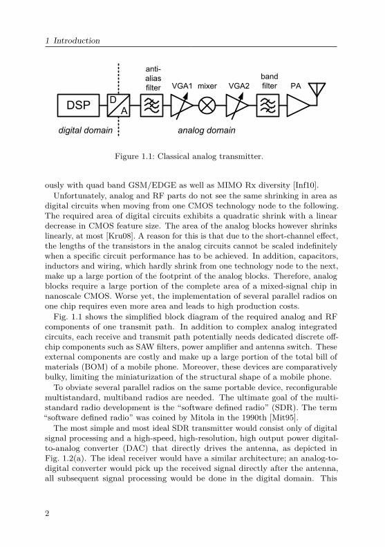
digital circuits when moving from one CMOS technology node to the following.The required area of digital circuits exhibits a quadratic shrink with a lineardecrease in CMOS feature size. The area of the analog blocks however shrinkslinearly, at most [Kru08]. A reason for this is that due to the short-channel effect,the lengths of the transistors in the analog circuits cannot be scaled indefinitelywhen a specific circuit performance has to be achieved. In addition, capacitors,inductors and wiring, which hardly shrink from one technology node to the next,make up a large portion of the footprint of the analog blocks. Therefore, analogblocks require a large portion of the complete area of a mixed-signal chip innanoscale CMOS. Worse yet, the implementation of several parallel radios onone chip requires even more area and leads to high production costs.Fig. 1.1 shows the simplified block diagram of the required analog and RF
components of one transmit path. In addition to complex analog integratedcircuits, each receive and transmit path potentially needs dedicated discrete off-chip components such as SAW filters, power amplifier and antenna switch. Theseexternal components are costly and make up a large portion of the total bill ofmaterials (BOM) of a mobile phone. Moreover, these devices are comparativelybulky, limiting the miniaturization of the structural shape of a mobile phone.
To obviate several parallel radios on the same portable device, reconfigurablemultistandard, multiband radios are needed. The ultimate goal of the multi-standard radio development is the “software defined radio” (SDR). The term“software defined radio” was coined by Mitola in the 1990th [Mit95].
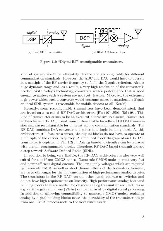
The most simple and most ideal SDR transmitter would consist only of digitalsignal processing and a high-speed, high-resolution, high output power digital-to-analog converter (DAC) that directly drives the antenna, as depicted inFig. 1.2(a). The ideal receiver would have a similar architecture; an analog-to-digital converter would pick up the received signal directly after the antenna,all subsequent signal processing would be done in the digital domain. This
2
DA
DSP
digital analog
(a) Ideal SDR transmitter
DSP
digital analog
DA
RF-DAC
(b) RF-DAC transmitter
Figure 1.2: “Digital RF” reconfigurable transmitters.
kind of system would be ultimately flexible and reconfigurable for differentcommunication standards. However, the ADC and DAC would have to operateat a multiple of the RF carrier frequency to fulfill the Nyquist criterion. Also, ahuge dynamic range and, as a result, a very high resolution of the converter isneeded. With today’s technology, converters with a performance that is goodenough to achieve such a system are not (yet) feasible. Moreover, the extremelyhigh power which such a converter would consume makes it questionable if suchan ideal SDR system is reasonable for mobile devices at all [Ken05].Recently, some reconfigurable transmitters have been demonstrated, that
are based on a so-called RF-DAC architecture [Elo+07; JS06; Tal+08]. Thiskind of transmitter seems to be an excellent alternative to classical transmitterarchitectures. RF-DAC based transmitters enable broadband OFDM transmis-sion and are reconfigurable for different mobile communication standards. TheRF-DAC combines D/A-converter and mixer in a single building block. As thisarchitecture still features a mixer, the digital blocks do not have to operate ata multiple of the carrier frequency. A simplified block diagram of an RF-DACtransmitter is depicted in Fig. 1.2(b). Analog baseband circuitry can be replacedwith digital, programmable blocks. Therefore, RF-DAC based transmitters area step towards Software Defined Radio (SDR).In addition to being very flexible, the RF-DAC architecture is also very well
suited for sub-65 nm CMOS nodes. Nanoscale CMOS nodes permit very fastand power-efficient digital circuits. The low supply voltages which are requiredby nanoscale CMOS as well as short channel effects of the transistors, however,are large challenges for the implementation of high-performance analog circuits.The transistors in the RF-DAC, on the other hand, operate as switches anddo not have high requirements on linearity. High-performance analog basebandbuilding blocks that are needed for classical analog transmitter architectures ase.g. variable gain amplifiers (VGAs) can be replaced by digital signal processing.In addition to achieving compatibility to nanoscale CMOS nodes, replacinganalog by digital building blocks makes the portability of the transmitter designfrom one CMOS process node to the next much easier.
3
1 Introduction
1.1 Goal of the work
The objective goal of this work is the implementation of a reconfigurable RF-DACbased transmitter. The transmitter should be capable of handling broadbandhigh-data-rate OFDM signals such as LTE or WLAN. In addition, the outputpower of the transmitter should be as high as possible in order to achieve a highintegration level and require only a low number of expensive external components,especially high gain power amplifier (PA) modules.
A suitable system architecture has to be found and performance requirementsfor the different building blocks have to be specified. Based on these findings,a circuit implementation of the mixed-signal transmitter frontend – and inparticular of the RF-DAC – has to be conducted. Finally, the fabricatedprototype has to be measured.
1.2 Structure of this thesis
The outline of this thesis is as follows:In chapter 2 the fundamentals of transmitters for wireless communications are
presented. The most important transmitter architectures are discussed and therelevant performance requirements as well as the most important performancemetrics are introduced. Furthermore, a brief introduction to modern broadbandOFDM-based wireless communication standards is given. It is found that OFDMhas quite high performance requirements on the RF frontend. Especially thehigh required peak to average power ratio is an issue.To decrease production costs and PCB area requirements of the transmitter,
it should be as highly integrated in a monolithic CMOS chip as possible. Highperformance and output power requirements make the integration of the PA anespecially difficult task. In chapter 3 the implementation of two different PAprototypes in 130 nm CMOS is discussed. The measurement results show a peaksaturated output power of more than 27 dBm at 1.9GHz. While this is sufficientfor connectivity devices like DECT, it is concluded from the measurements aswell as published results from other groups that it is not feasible to integratethe PA into a single-chip radio for cellular applications. Thus, subsequently onlytransmitter architectures with an additional external PA are considered.In chapter 4, the fundamentals of reconfigurable “direct-digital” RF-DAC
transmitters are presented. Different RF-DAC transmitter implementations andakin “digital-RF” architectures that can be found in literature are presented andcompared. General benefits and drawbacks of RF-DAC architectures, especiallythe quite high unwanted emission of spurious signals, are discussed. Finally,techniques to reduce the unwanted emission are introduced.
Subsequently, in chapter 5, the system concept of a transmitter that is basedon an RF-DAC based I/Q modulator is presented. Architectural choices are
4
1.2 Structure of this thesis
discussed and substantiated by Matlab system simulations. System performancerequirements are derived from the supported wideband OFDM-based commu-nication standards and the spectral emission masks that have to be fulfilled.Furthermore, performance specifications for the main digital, mixed-signal andRF building can be obtained from system simulations.Chapter 6 presents the circuit implementation of the mixed-signal and RF
frontend. Therefore, a 65 nm standard CMOS technology has been chosen as itenables the required performance of the digital blocks. The implementation ofthe RF-DAC as well as all other major building blocks is presented includingsimulation results. Additionally, layout considerations are discussed. Finally,simulation results of the complete RF-frontend are presented.
The measurement setup for the prototype IC as well as the major measurementresults is presented in chapter 7. The measurement results prove the feasibilityand potential of the RF-DAC transmitter concept. The RF-DAC transmitter iscapable of processing up to 40MHz wide 64QAM OFDM signals and fulfills theIEEE 802.11n spectral mask. The peak measured output power is 16 dBm.
Finally, chapter 8 concludes this thesis with a brief summary of the work thathas been done and gives an output to possible future improvements.
5

6
2 Fundamentals of Transmitters for WirelessCommunications
Together with the receiver, the transmitter forms the basis of every radio. TheRF transmitter performs modulation, upconversion of a low frequency (LF)baseband signal to the carrier frequency and power amplification of the RFoutput signal, before it is emitted by the antenna.
2.1 Basic transmitter architecture
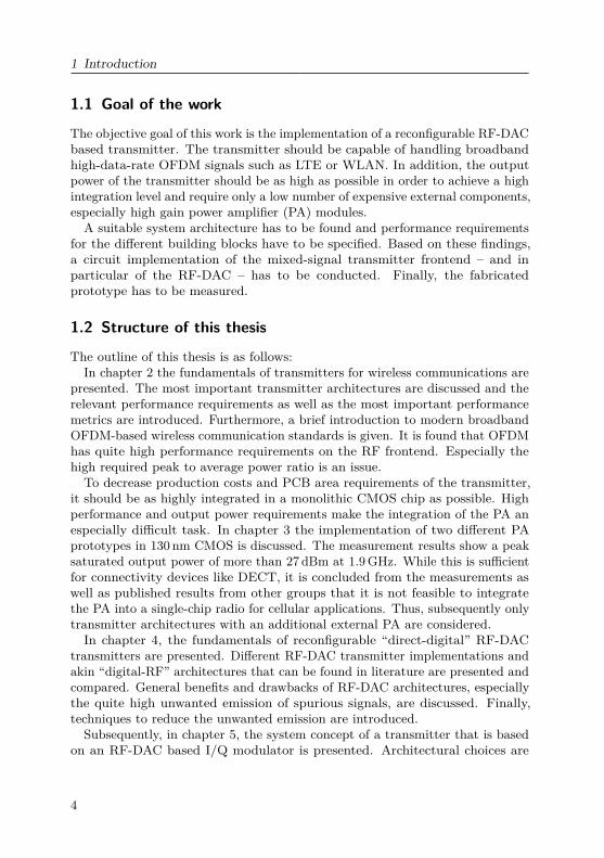
Almost all recent communication standards are based on digital signal modulation.The most commonly used RF transmitter architecture for this kind of system isthe direct conversion quadrature modulation transmitter, shown in Fig. 2.1. Fora direct conversion transmitter, the local oscillator (LO) frequency is equal tothe transmitted carrier frequency; thereby the frequency translation from LF toRF is done in one single step.The transmitter features a digital baseband processor which handles source
coding, channel coding, digital modulation and matched filtering of the datato be transmitted [McC10; Kam08]. The generated digital baseband signal iseventually translated to the analog domain, utilizing a digital-to-analog con-verter (DAC). The DAC obviously has to fulfill the Nyquist criterion, such thatan analog reconstruction filter can remove the DAC alias spectra. A quadra-ture upconversion mixer translates the I/Q baseband signals to the RF carrierfrequency.
DA
D
A
I(t)
Q(t)
LO 0o
90o
PAVGA
digital analog/RF
digital
signal
processing
Figure 2.1: Block diagram of a conventional analog quadrature RF transmitter.
7
2 Fundamentals of Transmitters for Wireless Communications
Variable gain amplifiers (VGAs) control the output power. These VGAs eithercan be implemented at baseband – before the mixer stage – or at RF, followingthe mixer. It is much easier to implement VGAs with high dynamic range atbaseband frequencies. Placing two separate amplifiers in the quadrature signalpaths, however, may create an I/Q amplitude imbalance. Therefore, sometimesit is preferable to do the power control at RF. Besides, some kind of driveris mostly needed anyway in order deliver the optimal signal amplitude to asubsequent power amplifier (PA).
The PA has the task to generate the required output power and deliver it tothe antenna. Typically, the PA is not integrated into the CMOS transceiver,but fabricated as an own chip in a high-performance GaAs or SiGe technology.The PA is connected to the antenna, which has a 50Ω input impedance, viaan impedance transformation network. Thereby, an optimum load impedance –which is generally lower than 50Ω – is presented to the PA, in order to maximizeits output power and energy efficiency [Cri06].Filters are needed to suppress unwanted out-of-band emissions. As the fil-
tering requirements for mobile communications are usually quite strict, high-performance “surface acoustic wave” (SAW) filters have to be used. Often,filtering is not only done at the PA output but also preceding the PA, in orderto improve its intermodulation performance.
2.2 Key RF transmitter performance measures andrequirements
Subsequently, the most important characteristics of RF transmitters and theirmeasures are briefly introduced.
2.2.1 Maximum output power
Obviously, the maximum output power Pout is one of the most importantperformance measures. Cellular standards define a maximum average outputpower which has to be achieved by the transmitter, as to guarantee properoperation even for inferior channel characteristics, e.g. when the handheld deviceis far away from the base station. Wireless connectivity standards such as WLANand Bluetooth only define a maximally permitted output power, such that atransmitting device does not disturb other devices which are located in somedistance but operate at the same frequency. The actually achieved maximumoutput power of these connectivity devices may be below this limit. Normally, theTx output power is defined at the input of the antenna or the antenna connector.For some communication standards, the “effective isotropically radiated power”(EIRP) is defined, which takes the antenna gain Gant into account. The EIRP is
8
2.2 Key RF transmitter performance measures and requirements
the amount of power that a theoretical isotropic radiation antenna would emit toproduce the peak power density measured in the direction of maximum antennagain. Thus, the EIRP can be calculated as
EIRP = Pout ·Gant (2.1)
The actual output power of the PA has to be higher than the maximumoutput power defined by the standard, as it will be damped by some dB by thesubsequent SAW filters and antenna switches.
For amplitude modulated signals a distinction must be made between maximumaverage output power and peak output power. The maximum average outputpower is the average over some period of time, e.g. one transmit burst. The peakoutput power, on the other hand, is the instantaneous maximum output powerwhich is only reached for a very short time duration. The fraction between thesetwo measures is called “Peak to Average Power Ratio” (PAPR) or “Crest factor”.
2.2.2 Dynamic rangeFor some cellular standards, not only the maximum average output power, butalso the minimum output power of a transmitter is defined. The dynamic rangeof the transmitter is given by:
dynamic range = Pout,max − Pout,min. (2.2)
Sometimes, also a power control step size (in dB) is given. For example, the3GPP WCDMA standard [3GP10] defines an dynamic range1 of 74 dB (+24 dBmto -50 dBm) and a power control step size of 1 dB for the mobile devices. Forcommunication standards which are based on a code division multiple accessscheme (CDMA) this accurate power control is very important to enable thebase station receiver to properly disaggregate the signal components which havebeen sent by different transmitters running at the same carrier frequency.
A sufficient dynamic range is normally achieved by cascading building blockswith several gain steps, such as VGAs and mixer. Also, power control can beimplemented with the DAC, if its amplitude resolution is sufficiently high.
2.2.3 Operational bandwidthThe required operational bandwidth is defined by the needed data rate andthe chosen modulation scheme. Different digital modulation techniques such asamplitude shift keying (ASK), frequency shift keying (FSK), phase shift keying(PSK), and orthogonal frequency division multiplex (OFDM) have different
1note that this definition of the dynamic range is based on average power levels and doesnot yet include the PAPR, which is approximately 5 dB for WCDMA.
9
2 Fundamentals of Transmitters for Wireless Communications
1dB
Pin
Pout
OIP3
IIP3IP1dB
OP1dBmain
signal
power IM power
(a) Pout vs. Pin
Pin
PAE
Pout[dBm]
Power
Added
Efficiency
40%
5%
(b) PAE vs. Pin
Figure 2.2: Amplifier nonlinearities (a) and power efficiency (b) versus inputpower.
spectral efficiencies. The spectral efficiency is defined as the number of bitswhich can be transmitted per time and bandwidth – typically measured at 20or 60 dBc signal roll-off. Obviously, a modulation scheme with high spectralefficiency is desirable. Nevertheless, trade-offs between spectral efficiency andthe required transmitter complexity and power consumption exist.The bandwidth of each building block must be high enough so that it does
not impair the signal quality. On the other hand, the filter bandwidths may notbe chosen too high, in order to suppress emissions at frequencies other than thewanted signal.
Modern OFDM-based communication standards support variable signal band-widths (see section 2.4). As a result, at least the baseband filters should beprogrammable in bandwidth, in order to achieve optimum performance.
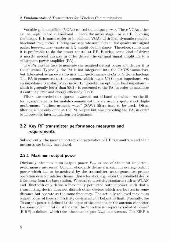
2.2.4 Linearity
For signals that have a non-constant envelope, a highly linear transmitter isessential to achieve a high signal quality and keep intermodulation distortion(IMD) low. For a linear amplifier the output signal is directly proportionalto the input signal. Real amplifiers, however, show clipping effects near theirmaximum capacity, leading to gain compression. An important measure forthis phenomenon is the 1 dB compression point, where the power gain of theamplifier is 1 dB below the small signal gain (see Fig. 2.2(a)). For amplitudemodulated signals, the peak output power must be well below this point to keep
10
2.2 Key RF transmitter performance measures and requirements
the signal quality high.If a sine-wave signal is applied to a nonlinear system, harmonics at multiple
frequencies of the fundamental are generated. As the system normally has a lowgain at these frequencies, harmonics are typically not measured directly as themulti-tone output of a single-tone input. Rather, a two-tone test is done.If several signals at different frequencies have to be amplified at the same
time, the nonlinearities introduced by gain compression lead to intermodulationbetween these signals. The third order intermodulation product of two sinusoidaltones at close frequencies ω1 and ω2 is of special interest, as it is notably high.Moreover, it can appear in-band, as the resulting tones are located close to theoriginal signals at ωIP3a = 2·ω1−ω2 and ωIP3b = 2·ω2−ω1. To specify the IMD,a performance metric called “third order intermodulation point” (IP3) is given[Raz97, p. 17 ff.]. The IP3 test takes advantage of the fact that the amplitude ofthe third order harmonic rises cubically, when the amplitudes of the fundamentaltones are increased linearly. Typically, the two input signals at ω1 and ω2 haveequal amplitudes A1 = A2 = A. When drawn in the logarithmic Pout vs. Pinplot (see Fig. 2.2(a)) straight lines result (at least in the weakly nonlinear regionof the system) with a slope of one for the power of the fundamental componentsand a slope of three for the IM3 product. The lines cross at the point, whichis defined as IP3. This point can either be specified as an input referred power(IIP3) or as an output referred power (OIP3), as shown in Fig. 2.2(a).
2.2.5 Power efficiency
Power efficiency (sometimes also termed “energy efficiency”), is important for amobile communication device as it determines battery run-time. The transmitterand especially the PA are typically the most power-hungry parts of a transceiver.Therefore, special emphasis has to be laid on maximizing the power efficiency ofthese building blocks.Different measures exist for the power efficiency
• The overall transmitter efficiency is defined as RF power Pout radiatedfrom the antenna divided by the total DC power Psupply drawn from thebattery
ηOTxE = PoutPsupply
· 100% (2.3)
• The (drain) output efficiency is the PA output power divided by the DCpower into the final PA stage
ηOE = PoutPsupply,PA
· 100% (2.4)
11
2 Fundamentals of Transmitters for Wireless Communications
• Often, the so-called “power added efficiency” (PAE) is given, when speci-fying the PA performance. It is the difference between the output powerPout and input power Pin of the PA, divided by the consumed DC power
PAE = Pout − PinPsupply,PA
· 100% (2.5)
For large power amplifications, PAE and ηOE are virtually the same.Power efficiency is highly dependent on the operation point of the PA. A
typical PAE versus Pin curve for a linear PA, like a class A, AB or B amplifier, isshown in Fig. 2.2(b). As can be seen, a high efficiency can only be achieved, whenthe PA is operated in compression, close to its maximum saturated output power.For amplitude modulated signals, however, a PA operation in compression is notpracticable because of the required linearity, as discussed above. For this reason,constant envelope modulated signals typically permit a higher power efficiencythan amplitude modulated signals. Moreover, the system costs for the formermay be much lower, as the PA output power capacity can be much reduced.
2.2.6 Unwanted emissionsUnwanted emissions are a major issue of every RF transmitter. To minimizeinterference with other wireless communications systems, emissions at otherfrequencies than the wanted signal shall not be too high. Therefore, mostcommunication standards place stringent requirements on both out-of-band andout-of-channel emissions.
The cause of unwanted emissions can be separated into two categories: close-to-carrier and far-off noise. Close-to-carrier noise is dominated by IMD, asillustrated in Fig. 2.3 [Ken05]. Main contributor to IMD is the PA. Typically,cellular standards define the maximum IMD power in the neighboring channels.These measurements are done with real, modulated signals instead of the abovegiven IMD definitions with sinusoidal signals. Therefore, the maximum unwantedsignal power in a channel bandwidth, one channel away from the wanted signal,is defined. This power is divided by the power in the wanted channel and givenas “adjacent channel power ratio” (ACPR). Noise in the adjacent channel isdominated by the third order IMD product [Anr01]. Also, sometimes the powerin a bandwidth two channels away is defined as “alternate channel power ratio”.In terms of the IMD measurements, a fifths order product may correspond tothe alternate channel power ratio.
In addition to IMD, LO phase noise spreads out the wanted signal in frequency,which can lead to a violation of the spectral mask. This is especially an issue fornarrowband systems like GSM, leading to a high phase noise to signal bandwidthratio. To reduce phase noise, a high-performance VCO as well as an adequatePLL architecture is needed.
12
2.2 Key RF transmitter performance measures and requirements
Frequency
Am
plit
ud
e
Ch
an
ne
l
DAC and
upconversion
noise dominate
IMD noise
dominates
IMD noise
dominates
DAC and
upconversion noise
dominate
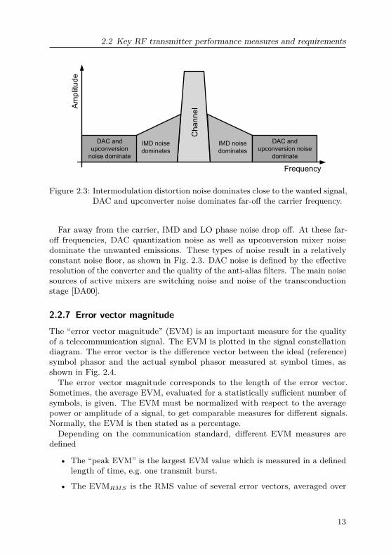
Figure 2.3: Intermodulation distortion noise dominates close to the wanted signal,DAC and upconverter noise dominates far-off the carrier frequency.
Far away from the carrier, IMD and LO phase noise drop off. At these far-off frequencies, DAC quantization noise as well as upconversion mixer noisedominate the unwanted emissions. These types of noise result in a relativelyconstant noise floor, as shown in Fig. 2.3. DAC noise is defined by the effectiveresolution of the converter and the quality of the anti-alias filters. The main noisesources of active mixers are switching noise and noise of the transconductionstage [DA00].
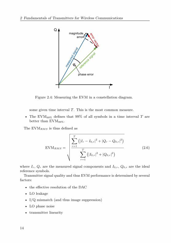
2.2.7 Error vector magnitudeThe “error vector magnitude” (EVM) is an important measure for the qualityof a telecommunication signal. The EVM is plotted in the signal constellationdiagram. The error vector is the difference vector between the ideal (reference)symbol phasor and the actual symbol phasor measured at symbol times, asshown in Fig. 2.4.The error vector magnitude corresponds to the length of the error vector.
Sometimes, the average EVM, evaluated for a statistically sufficient number ofsymbols, is given. The EVM must be normalized with respect to the averagepower or amplitude of a signal, to get comparable measures for different signals.Normally, the EVM is then stated as a percentage.Depending on the communication standard, different EVM measures are
defined
• The “peak EVM” is the largest EVM value which is measured in a definedlength of time, e.g. one transmit burst.
• The EVMRMS is the RMS value of several error vectors, averaged over
13
2 Fundamentals of Transmitters for Wireless Communications
I
Q
φm
easu
red s
ignal
refe
renc
e sign
al
phase error
erro
r vecto
r
magnitude
error
Figure 2.4: Measuring the EVM in a constellation diagram.
some given time interval T . This is the most common measure.
• The EVM99% defines that 99% of all symbols in a time interval T arebetter than EVM99%.
The EVMRMS is thus defined as
EVMRMS =
√√√√√√√√√T∑r=1
(|Ir − I0,r|2 + |Qr −Q0,r|2
)T∑r=1
(|I0,r|2 + |Q0,r|2
) (2.6)
where Ir, Qr are the measured signal components and I0,r, Q0,r are the idealreference symbols.
Transmitter signal quality and thus EVM performance is determined by severalfactors:
• the effective resolution of the DAC
• LO leakage
• I/Q mismatch (and thus image suppression)
• LO phase noise
• transmitter linearity
14
2.3 Important Transmitter topologies
In addition to evaluating the raw EVM value, looking at the constellationdiagram can give useful hints, what the limiting factors for the signal quality are.LO phase noise, for example, only generates a phase error, but no magnitudeerror. Therefore, the measured symbols are lying on a circle that goes throughthe reference symbols. I/Q mismatch on the other hand can be observed as adeformation of the constellation in the I/Q plane. It is not a square any more,but rather a rectangle with unevenly long sides.
For simulations and measurements on system level, including baseband signalprocessing, the signal quality is also often specified as bit error rate (BER).Anyhow, BER simulations and measurements do only allow to evaluate theperformance of the complete transmitter chain including digital baseband pro-cessing. It is not possible to evaluate the influence of only the RF frontend onthe BER. A BER analysis requires simulations over a very long system time,which is almost not possible for the RF frontend because of the small requiredsimulation time steps.
2.3 Important Transmitter topologies
Subsequently, some of the most important and popular transmitter architecturesshall be introduced.
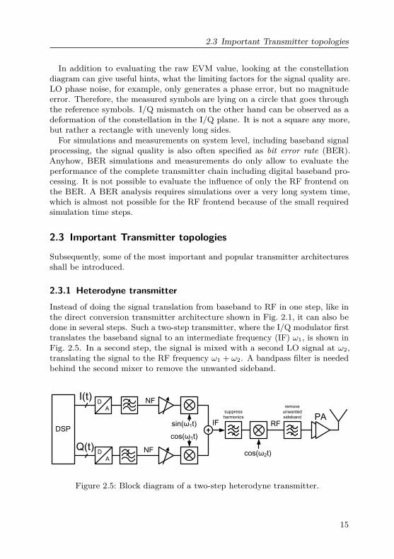
2.3.1 Heterodyne transmitterInstead of doing the signal translation from baseband to RF in one step, like inthe direct conversion transmitter architecture shown in Fig. 2.1, it can also bedone in several steps. Such a two-step transmitter, where the I/Q modulator firsttranslates the baseband signal to an intermediate frequency (IF) ω1, is shown inFig. 2.5. In a second step, the signal is mixed with a second LO signal at ω2,translating the signal to the RF frequency ω1 + ω2. A bandpass filter is neededbehind the second mixer to remove the unwanted sideband.
DA
D
A
I(t)
Q(t)
PA
NF
DSPsin(ω1t)
cos(ω1t)
cos(ω2t)
IF RF
NF
suppress
harmonics
remove
unwanted
sideband
Figure 2.5: Block diagram of a two-step heterodyne transmitter.
15
2 Fundamentals of Transmitters for Wireless Communications
The two-step transmitter of Fig. 2.5 is the transmitter equivalent to theheterodyne receiver architecture.
The heterodyne transmitter architecture has some advantages over the homo-dyne architecture. First, homodyne transmitters can suffer from so-called “VCOpulling” or “injection locking” [Raz97, p. 153 ff.]. This effect can occur, whenthe strong PA signal output leaks back into the VCO, if the latter one is notshielded well enough. The VCO then can be disturbed by the “noisy” modulatedPA output. This problem can be reduced if the I/Q signal is generated by afactor-of-two frequency division, as the VCO then is a multiple of the PA outputfrequency. For heterodyne transmitters VCO pulling is no problem, as the PAoutput frequency may be chosen independently from the IF frequency. As thesecond LO frequency is different from the RF frequency, also LO feedthrough isno problem.
Second, two-step transmitters usually have a better I and Q matching, as themodulator is running at a lower frequency. A channel filter at IF may be usedto reduce the transmitted noise and spurs at adjacent channels.Nevertheless, this architecture can hardly be found in modern integrated
transmitter solutions, as the large number of needed components leads to highcosts. One main obstacle are the IF filters which have to be implemented asexternal SAW filters to get a high quality factor. Thus, they are bulky andespecially expensive.
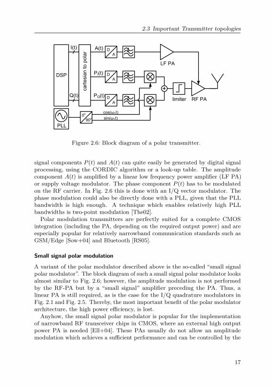
2.3.2 Polar modulatorPolar modulation originates in a technique called “Envelope Elimination andRestoration” which was first introduced by Kahn in 1952 [Kah52]. Polar mod-ulator transmitters are based on the decomposition of the RF signal into amagnitude and phase component. The phase component then is an RF signalbut has a constant envelope. The magnitude component is essentially the en-velope of the modulated signal and is at LF. The RF signal reconstruction isdone with an RF power amplifier stage close to the antenna. The input signal ofthis amplifier is the phase modulated signal, while the amplitude modulation isdone by changing the supply voltage. As the RF signal component contains onlyphase information, a PA which linearly amplifies the input signal is not required.A nonlinear power amplifier with high power efficiency can be used. Typically, aclass E PA is utilized, whose output voltage is linearly proportional to its supplyvoltage [RS06]. All linearity requirements are shifted to the low frequency parts,namely the supply voltage regulators, where they are much easier to achieve.The whole RF path may be nonlinear. Therefore, the power efficiency of thepolar modulator architecture is relatively high, while still allowing amplitudemodulation.
A possible implementation of a polar modulator is shown in Fig. 2.6. The polar
16
2.3 Important Transmitter topologies
DA
D
A
I(t)
Q(t)
DSP
sin(ω1t)
cos(ω1t)
ca
rte
sia
n to
po
lar
PLL
0o
90o
DA
LF PA
RF PA
A(t)
PI(t)
PQ(t)limiter
Figure 2.6: Block diagram of a polar transmitter.
signal components P (t) and A(t) can quite easily be generated by digital signalprocessing, using the CORDIC algorithm or a look-up table. The amplitudecomponent A(t) is amplified by a linear low frequency power amplifier (LF PA)or supply voltage modulator. The phase component P (t) has to be modulatedon the RF carrier. In Fig. 2.6 this is done with an I/Q vector modulator. Thephase modulation could also be directly done with a PLL, given that the PLLbandwidth is high enough. A technique which enables relatively high PLLbandwidths is two-point modulation [The02].Polar modulation transmitters are perfectly suited for a complete CMOS
integration (including the PA, depending on the required output power) and areespecially popular for relatively narrowband communication standards such asGSM/Edge [Sow+04] and Bluetooth [RS05].
Small signal polar modulation
A variant of the polar modulator described above is the so-called “small signalpolar modulator”. The block diagram of such a small signal polar modulator looksalmost similar to Fig. 2.6; however, the amplitude modulation is not performedby the RF-PA but by a “small signal” amplifier preceding the PA. Thus, alinear PA is still required, as is the case for the I/Q quadrature modulators inFig. 2.1 and Fig. 2.5. Thereby, the most important benefit of the polar modulatorarchitecture, the high power efficiency, is lost.
Anyhow, the small signal polar modulator is popular for the implementationof narrowband RF transceiver chips in CMOS, where an external high outputpower PA is needed [Ell+04]. These PAs usually do not allow an amplitudemodulation which achieves a sufficient performance and can be controlled by the
17
2 Fundamentals of Transmitters for Wireless Communications
ba
se
ba
nd
sig
na
l
pro
ce
ssin
g
+φ0
-φ0
Sp(t)
S1(t)
S2(t)
PA1
PA2
power
combiner
S(t)
(a) LINC block diagram
I
Q
S1
S2S
φ0 φ0
(b) signal combination principle
Figure 2.7: Simplified block diagram of a LINC transmitter and outphasingprinciple.
CMOS transceiver chip.Although lacking a substantial power efficiency benefit compared to I/Q
modulators, the small signal polar still can have some relevant advantages:
• The narrowband PLL transfer function leads to a good filtering of theupconverted noise. Thus, the filtering requirements between transceiverchip and PA may be relaxed. It is even possible to obviate the need fora SAW filter at the transceiver output if the unwanted emissions of thepolar modulator are low enough.
• The required die area for the modulator may be smaller than for anI/Q modulator, as only one amplitude path is required; however, a morecomplex PLL is needed.
• I/Q mismatch is no issue.
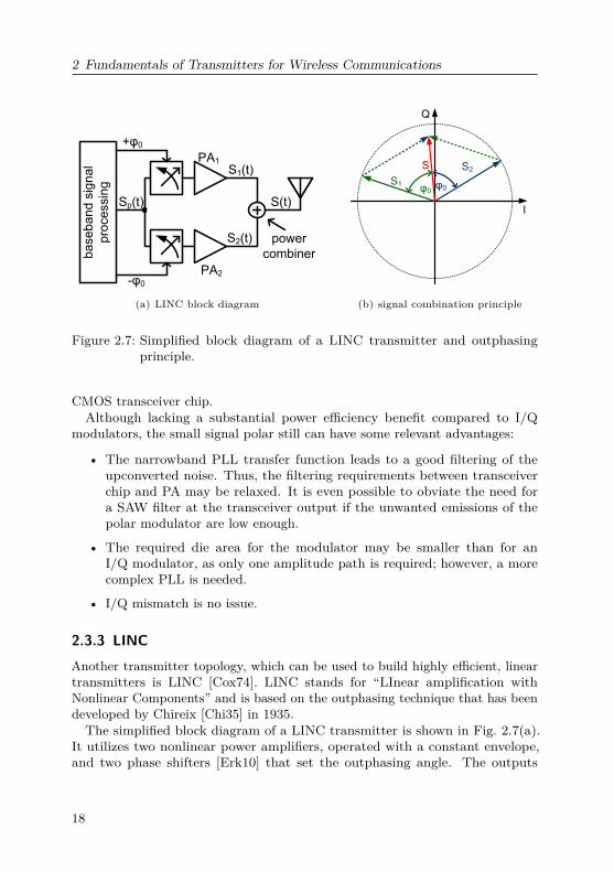
2.3.3 LINCAnother transmitter topology, which can be used to build highly efficient, lineartransmitters is LINC [Cox74]. LINC stands for “LInear amplification withNonlinear Components” and is based on the outphasing technique that has beendeveloped by Chireix [Chi35] in 1935.The simplified block diagram of a LINC transmitter is shown in Fig. 2.7(a).
It utilizes two nonlinear power amplifiers, operated with a constant envelope,and two phase shifters [Erk10] that set the outphasing angle. The outputs
18
2.4 OFDM and its use in wireless communications
are combined with a power combiner. Both amplifiers always have outputsignals S1(t) and S2(t) at the maximum amplitude of the PAs. As a result, thePAs are operated at their maximum power efficiency. Nevertheless, a linearamplitude modulated signal S(t) can be generated by modulating the phasedifference between the two output signals, therefore the name LINC. The principleoperation of this outphasing technique is depicted in Fig. 2.7(b). Obviously,output powers up to twice the capacity of a single PA can be realized.For modern CMOS technologies the phase shifters may also be implemented
in the digital domain. In this case, the phase shifter resolution, however, mustbe high enough so that the amplitude resolution requirements can be fulfilled.The main issue of the LINC concept is the implementation of the power
combiner. The most common approach is to use a Wilkinson combiner. Whileproviding excellent linearity and isolation between the PAs, for small neededoutput powers, the Wilkinson combiner sinks all excessive generated PA power.As a result, for high PAPRs this topology in fact does have a lower powerefficiency than a simple class AB amplifier [NG08]
As an alternative to the Wilkinson combiner, a lossless power combiner couldalso be used. In this case, however, the PA outputs are not isolated, leading tosome kind of active load-pulling and, as a consequence, to a nonlinear output.Summarizing, it can be said that LINC does not have a significant power
efficiency advance over linear class AB PAs, although highly efficient nonlinearPAs can be used. Nevertheless, linear PAs need to have a higher output powercapacity to achieve the same linear output power as a LINC system.The advances in CMOS technology that permit building high performance
signal processing and PAs on the same chip, recently have led to an increasedresearch in the field of LINC [Hei+09].
2.4 The OFDM technology and its use in wirelesscommunications
Just as for wireline communications, also for mobile communications there isa trend towards ever increasing data rates. As bandwidth is quite limitedfor wireless communications, modulation techniques with a great bandwidthefficiency (measured as bits per second and Hertz) are therefore needed. Amodulation scheme which fulfills this need and has gotten increasingly popularin recent years is Orthogonal Frequency Division Multiplex (OFDM). It is usedfor almost all modern broadband mobile communication standards, like WLAN(IEEE 802.11a/g/n), WiMax mobile (IEEE 802.16e), 3GPP LTE and Bluetooth3.0. Thus, the basic principles and characteristics of OFDM and its consequenceson the RF frontend shall be briefly discussed subsequently.
19
2 Fundamentals of Transmitters for Wireless Communications
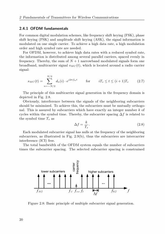
2.4.1 OFDM fundamentalsFor common digital modulation schemes, like frequency shift keying (FSK), phaseshift keying (PSK) and amplitude shift keying (ASK), the signal information ismodulated on one single carrier. To achieve a high data rate, a high modulationorder and high symbol rate are needed.For OFDM, however, to achieve high data rates with a reduced symbol rate,
the information is distributed among several parallel carriers, spaced evenly infrequency. Thereby, the sum of N + 1 narrowband modulated signals form onebroadband, multicarrier signal sMC(t), which is located around a radio carriersignal:
sMC(t) =N/2∑
n=−N/2
dn(i) · ej2πfnt for iTs ≤ t ≤ (i+ 1)Ts (2.7)
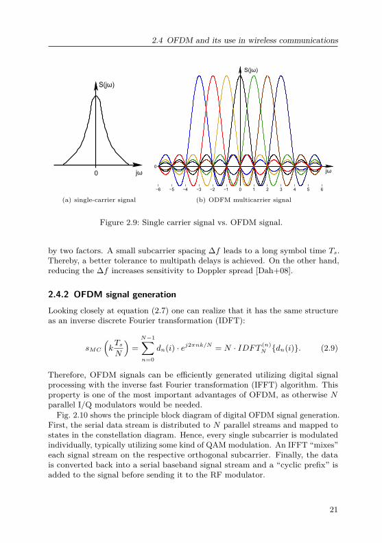
The principle of this multicarrier signal generation in the frequency domain isdepicted in Fig. 2.8.Obviously, interference between the signals of the neighboring subcarriers
should be minimized. To achieve this, the subcarriers must be mutually orthogo-nal. This is assured by subcarriers which have exactly an integer number k ofcycles within the symbol time. Thereby, the subcarrier spacing ∆f is related tothe symbol time Ts as
∆f = k
Ts. (2.8)
Each modulated subcarrier signal has nulls at the frequency of the neighboringsubcarriers, as illustrated in Fig. 2.9(b), thus the subcarriers are intercarrierinterference (ICI) free.The total bandwidth of the OFDM system equals the number of subcarriers
times the subcarrier spacing. The selected subcarrier spacing is constrained
fcenter f1f-1Δf
fN/2f-N/2 f
lower subcarriers higher subcarriersca
rrie
r
fre
qu
en
cy
Figure 2.8: Basic principle of multiple subcarrier signal generation.
20
2.4 OFDM and its use in wireless communications
S(jω)
jω0
(a) single-carrier signal−6 −5 −4 −3 −2 −1 0 1 2 3 4 5 6
0
S(jω)
jω
(b) ODFM multicarrier signal
Figure 2.9: Single carrier signal vs. OFDM signal.
by two factors. A small subcarrier spacing ∆f leads to a long symbol time Ts.Thereby, a better tolerance to multipath delays is achieved. On the other hand,reducing the ∆f increases sensitivity to Doppler spread [Dah+08].
2.4.2 OFDM signal generation
Looking closely at equation (2.7) one can realize that it has the same structureas an inverse discrete Fourier transformation (IDFT):
sMC
(kTsN
)=N−1∑n=0
dn(i) · ej2πnk/N = N · IDFT (n)N dn(i). (2.9)
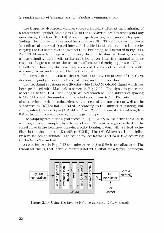
Therefore, OFDM signals can be efficiently generated utilizing digital signalprocessing with the inverse fast Fourier transformation (IFFT) algorithm. Thisproperty is one of the most important advantages of OFDM, as otherwise Nparallel I/Q modulators would be needed.
Fig. 2.10 shows the principle block diagram of digital OFDM signal generation.First, the serial data stream is distributed to N parallel streams and mapped tostates in the constellation diagram. Hence, every single subcarrier is modulatedindividually, typically utilizing some kind of QAM modulation. An IFFT “mixes”each signal stream on the respective orthogonal subcarrier. Finally, the datais converted back into a serial baseband signal stream and a “cyclic prefix” isadded to the signal before sending it to the RF modulator.
21
2 Fundamentals of Transmitters for Wireless Communications
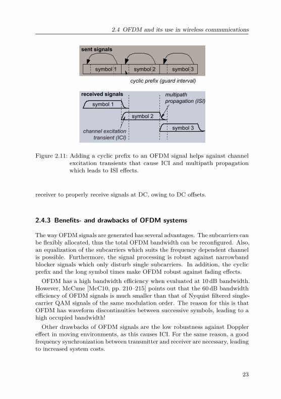
The frequency dependent channel causes a transient effect at the beginning ofa transmitted symbol, leading to ICI as the subcarriers are not orthogonal anymore during this time [Kam08]. Also, multipath propagation causes delay spread(fading), leading to inter symbol interference (ISI). Therefore, a cyclic prefix(sometimes also termed “guard interval”) is added to the signal. This is done bycopying the last samples of the symbol to its beginning, as illustrated in Fig. 2.11.As OFDM signals are cyclic by nature, this can be done without generatinga discontinuity. The cyclic prefix must be longer than the channel impulseresponse. It gives time for the transient effects and thereby suppresses ICI andISI effects. However, this obviously comes at the cost of reduced bandwidthefficiency, as redundancy is added to the signal.The signal demodulation in the receiver is the inverse process of the above
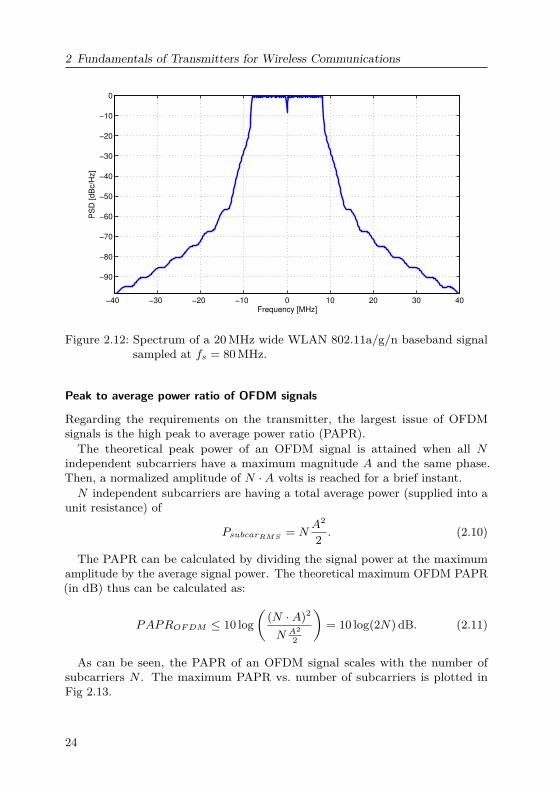
discussed signal generation scheme, utilizing an FFT algorithm.The baseband spectrum of a 20MHz wide 64QAM OFDM signal which has
been produced with Matlab® is shown in Fig. 2.12. The signal is generatedaccording to the IEEE 802.11a/g/n WLAN standard. The subcarrier spacingis 312.5 kHz and the number of allocated subcarriers is 52. The total numberof subcarriers is 64; the subcarriers at the edges of the spectrum as well as thesubcarrier at DC are not allocated. According to the subcarrier spacing, onecore symbol length is Ts = (312.5 kHz)−1 = 3.2µs. The guard interval length is0.8µs, leading to a complete symbol length of 4µs.
The sampling rate of the signal shown in Fig. 2.12 is 80MHz, hence the 20MHzwide signal is oversampled by a factor of four. To achieve a good roll-off of thesignal slope in the frequency domain, a pulse-forming is done with a raised-cosinefilter in the time domain [Kam08, p. 612 ff.]. The OFDM symbol is multipliedby a raised-cosine window. The cosine roll-off factor is set to 0.0625 accordingto the WLAN standard.As can be seen in Fig. 2.12 the subcarrier at f = 0Hz is not allocated. The
reason for this is, that it would require substantial effort for a typical homodyne
symbol
generation
se
ria
l to
pa
ralle
l
pa
ralle
l to
se
ria
l
sym
bo
l to
sta
te
ma
pp
ing
IFF
T
ad
d c
yclic
pre
fix
1
2
N
3
1
2
3
1
2
N
3
OFDM
I
Q
OFDM
signal s(t)RF
modulator
RF
carrier
N
I
Q
Figure 2.10: Using the inverse FFT to generate OFDM signals.
22
2.4 OFDM and its use in wireless communications
sent signals
received signals
symbol 1 symbol 2 symbol 3
cyclic prefix (guard interval)
channel excitationtransient (ICI)
multipathpropagation (ISI)symbol 1
symbol 2
symbol 3
Figure 2.11: Adding a cyclic prefix to an OFDM signal helps against channelexcitation transients that cause ICI and multipath propagationwhich leads to ISI effects.
receiver to properly receive signals at DC, owing to DC offsets.
2.4.3 Benefits- and drawbacks of OFDM systems
The way OFDM signals are generated has several advantages. The subcarriers canbe flexibly allocated, thus the total OFDM bandwidth can be reconfigured. Also,an equalization of the subcarriers which suits the frequency dependent channelis possible. Furthermore, the signal processing is robust against narrowbandblocker signals which only disturb single subcarriers. In addition, the cyclicprefix and the long symbol times make OFDM robust against fading effects.OFDM has a high bandwidth efficiency when evaluated at 10 dB bandwidth.
However, McCune [McC10, pp. 210–215] points out that the 60 dB bandwidthefficiency of OFDM signals is much smaller than that of Nyquist filtered single-carrier QAM signals of the same modulation order. The reason for this is thatOFDM has waveform discontinuities between successive symbols, leading to ahigh occupied bandwidth!Other drawbacks of OFDM signals are the low robustness against Doppler
effect in moving environments, as this causes ICI. For the same reason, a goodfrequency synchronization between transmitter and receiver are necessary, leadingto increased system costs.
23
2 Fundamentals of Transmitters for Wireless Communications
−40 −30 −20 −10 0 10 20 30 40
−90
−80
−70
−60
−50
−40
−30
−20
−10
0
Frequency [MHz]
PS
D [
dB
c/H
z]
Figure 2.12: Spectrum of a 20MHz wide WLAN 802.11a/g/n baseband signalsampled at fs = 80 MHz.
Peak to average power ratio of OFDM signals
Regarding the requirements on the transmitter, the largest issue of OFDMsignals is the high peak to average power ratio (PAPR).The theoretical peak power of an OFDM signal is attained when all N
independent subcarriers have a maximum magnitude A and the same phase.Then, a normalized amplitude of N ·A volts is reached for a brief instant.N independent subcarriers are having a total average power (supplied into a
unit resistance) of
PsubcarRMS = NA2
2 . (2.10)
The PAPR can be calculated by dividing the signal power at the maximumamplitude by the average signal power. The theoretical maximum OFDM PAPR(in dB) thus can be calculated as:
PAPROFDM ≤ 10 log(
(N ·A)2
N A22
)= 10 log(2N) dB. (2.11)
As can be seen, the PAPR of an OFDM signal scales with the number ofsubcarriers N . The maximum PAPR vs. number of subcarriers is plotted inFig 2.13.
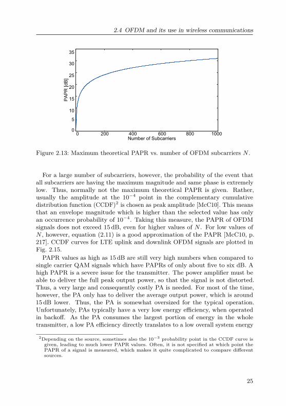
24
2.4 OFDM and its use in wireless communications
0
5
10
15
20
25
30
35
0 200 400 600 800 1000
PA
PR
[d
B]
Number of Subcarriers
Figure 2.13: Maximum theoretical PAPR vs. number of OFDM subcarriers N .
For a large number of subcarriers, however, the probability of the event thatall subcarriers are having the maximum magnitude and same phase is extremelylow. Thus, normally not the maximum theoretical PAPR is given. Rather,usually the amplitude at the 10−4 point in the complementary cumulativedistribution function (CCDF)2 is chosen as peak amplitude [McC10]. This meansthat an envelope magnitude which is higher than the selected value has onlyan occurrence probability of 10−4. Taking this measure, the PAPR of OFDMsignals does not exceed 15 dB, even for higher values of N . For low values ofN , however, equation (2.11) is a good approximation of the PAPR [McC10, p.217]. CCDF curves for LTE uplink and downlink OFDM signals are plotted inFig. 2.15.
PAPR values as high as 15 dB are still very high numbers when compared tosingle carrier QAM signals which have PAPRs of only about five to six dB. Ahigh PAPR is a severe issue for the transmitter. The power amplifier must beable to deliver the full peak output power, so that the signal is not distorted.Thus, a very large and consequently costly PA is needed. For most of the time,however, the PA only has to deliver the average output power, which is around15 dB lower. Thus, the PA is somewhat oversized for the typical operation.Unfortunately, PAs typically have a very low energy efficiency, when operatedin backoff. As the PA consumes the largest portion of energy in the wholetransmitter, a low PA efficiency directly translates to a low overall system energy
2Depending on the source, sometimes also the 10−3 probability point in the CCDF curve isgiven, leading to much lower PAPR values. Often, it is not specified at which point thePAPR of a signal is measured, which makes it quite complicated to compare differentsources.
25
2 Fundamentals of Transmitters for Wireless Communications
symbol
generation
se
ria
l to
pa
ralle
l
pa
ralle
l to
se
ria
l
sym
bo
l to
sta
te
ma
pp
ing
IFF
T
ad
d c
yclic
pre
fix
1
2
N
3
1
2
3
1
2
M
3
SC-FDMA
I
Q
SC-FDMA
signal s(t)RF
modulator
RF
carrier
N
I
QFF
T
1
2
3
M
Figure 2.14: SC-FDMA baseband encoding.
efficiency. The problem of the PA is thoroughly discussed in chapter 3.
2.4.4 EVM calculations in OFDM systemsEVM calculations are a bit special for OFDM systems, as there is an ownconstellation diagram for each subcarrier. Therefore, EVM is first calculatedseparately for each subcarrier. Afterwards, the EVM values are averaged overall subcarriers and an EVMrms is given [McK+04].
2.4.5 OFDM-based communications standardsSeveral modern mobile communication standards for high data rate transmissionare based on OFDM. The most important ones are probably Wireless LAN(IEEE 802.11x), WiMAX mobile (IEEE 802.16e), and 3GPP LTE. The propertiesof these standards, which are relevant for the RF transmitter frontend, aresummarized in Table 2.1.
LTE and SC-FDMA
3GPP long-term evolution (LTE) is the successor of the UMTS/WCDMA mobilestandard. While UMTS – including the “High Speed Packet Access” (HSPA)high data rate enhancements – is based on single-carrier QAM modulation, LTEis based on OFDM.LTE uses different modulation types for downlink (from the base station
to the mobile device) and uplink (from the mobile device to the base station)transmission. The downlink uses ordinary OFDM, the uplink on the other handuses a special signal type termed “Single Carrier Frequency Division MultipleAccess” (SC-FDMA). Although it is called “single carrier”, it really is a form ofOFDM with some modifications in the signal processing.
26
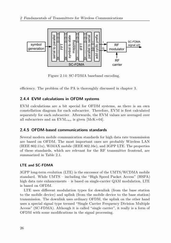
2.4 OFDM and its use in wireless communications
The SC-FDMA signal generation is shown in Fig. 2.14. It is derived from theregular OFDM architecture, shown in Fig. 2.10. The first step in SC-FDMAmodulation, however, is to perform an additional M-point DFT [Myu+06]. Thisstep is used to “scramble” the regular QAM signal state into another set ofsignal states for each subcarrier. Therefore, this type of transmission schemeis also called “DFT-spread OFDM” (DFTS-OFDM). Afterwards, the size-NIDFT, with N>M, generates the regular OFDM waveform. The unused inputsof the IDFT are set to zero, hence creating unallocated subcarriers. The DFT“scrambling” leads to a reduced probability that all subcarriers align to a largesignal amplitude peak.By applying DFT-spread OFDM, the PAPR can be reduced in the order
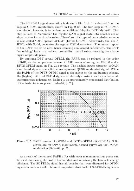
of 3 dB, as the comparison between CCDF curves of an regular OFDM and aDFTS-OFDM signal in Fig. 2.15 reveals. The dashed curves represent 16QAMmodulated signals, the solid curves represent QPSK modulated signal. Whilethe PAPR of the DFTS-OFDM signal is dependent on the modulation scheme,the (higher) PAPR of OFDM signals is relatively constant, as for the latter allsubcarriers are independent, leading to an approximately exponential distributionof the instantaneous power [Dah+08, p. 76].
Figure 2.15: PAPR curves of OFDM and DTFS-OFDM (SC-FDMA). Solidcurves are for QPSK modulation, dashed curves are for 16QAMmodulation [Dah+08, p. 75].
As a result of the reduced PAPR a PA with lower maximum output power canbe used, decreasing the cost of the handset and increasing the handsets energyefficiency. The SC-FDMA signal has all benefits that were discussed for OFDMsignals in section 2.4.3. The most important drawback of SC-FDMA signals is
27

2 Fundamentals of Transmitters for Wireless Communications
the increased digital signal processing. The largest effort, however, has to bedone on the receiver side, which is the base station. As this is not battery driven,in contrast to the mobile device, the increased power consumption at this pointis not too critical.
Although the PAPR is reduced by about 3 dB for SC-FDMA signals comparedto OFDM, it is still much higher than for comparable QAM signals. With aPAPR of nearly 10 dB the LTE power amplifier must still be overscaled bya factor of 10. To generate a maximum average output power of +23 dBm(200mW), it must be capable to deliver a linear peak output power of +33 dBm(2W).
28
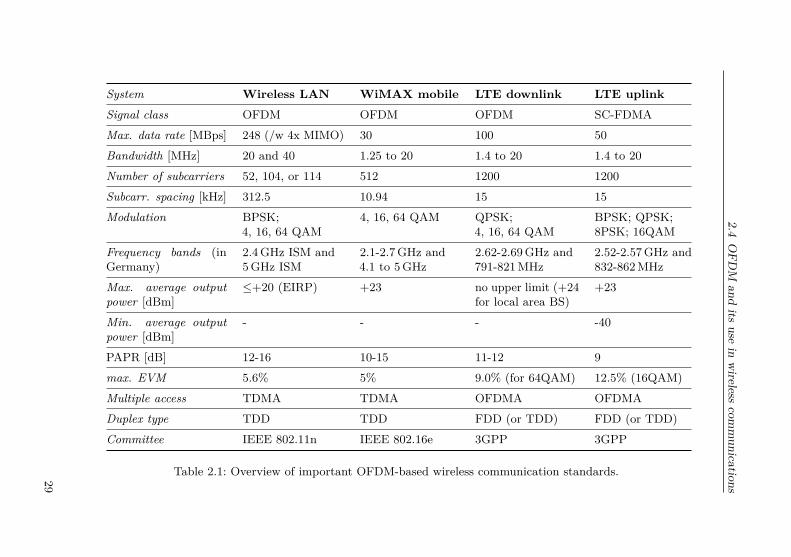
2.4OFD
Mand
itsuse
inwireless
communications
System Wireless LAN WiMAX mobile LTE downlink LTE uplinkSignal class OFDM OFDM OFDM SC-FDMAMax. data rate [MBps] 248 (/w 4x MIMO) 30 100 50Bandwidth [MHz] 20 and 40 1.25 to 20 1.4 to 20 1.4 to 20Number of subcarriers 52, 104, or 114 512 1200 1200Subcarr. spacing [kHz] 312.5 10.94 15 15Modulation BPSK;
4, 16, 64 QAM4, 16, 64 QAM QPSK;
4, 16, 64 QAMBPSK; QPSK;8PSK; 16QAM
Frequency bands (inGermany)
2.4GHz ISM and5GHz ISM
2.1-2.7GHz and4.1 to 5GHz
2.62-2.69GHz and791-821MHz
2.52-2.57GHz and832-862MHz
Max. average outputpower [dBm]
≤+20 (EIRP) +23 no upper limit (+24for local area BS)
+23
Min. average outputpower [dBm]
- - - -40
PAPR [dB] 12-16 10-15 11-12 9max. EVM 5.6% 5% 9.0% (for 64QAM) 12.5% (16QAM)Multiple access TDMA TDMA OFDMA OFDMADuplex type TDD TDD FDD (or TDD) FDD (or TDD)Committee IEEE 802.11n IEEE 802.16e 3GPP 3GPP
Table 2.1: Overview of important OFDM-based wireless communication standards.29

30
3 Challenges for Integrated CMOS PowerAmplifiers
3.1 Introduction
The power amplifier (PA) is one of the most important parts of every RFtransmitter. Most PAs for mobile devices are based on high-performance SiGe orGaAs technologies, which leads to quite high production costs. The transceiverand baseband circuitry on the other hand are preferably designed using standardlow-cost CMOS technology. Typically, for each communication standard andfrequency band which the mobile communication device supports a dedicated PAis needed. For example, according to iSuppli [iSu10], Apple’s iPhone 4 containsfive different PA modules that are required to support the different GSM/EDGEand WCDMA frequency bands. Each PA module again potentially containsseveral different PA chips. This leads to an increased bill of materials and alsoneeds a large PCB area.PAs in standard CMOS would allow the full integration of a complete radio
system on a single chip [Haj05], resulting in considerable cost and size reductions.PAs in modern sub-micron CMOS processes with performances approachingSiGe and GaAs PAs are therefore of great interest, although their design isa big challenge. As CMOS is scaled down the roadmap, the design of highperformance PAs becomes more and more demanding. This is mainly dueto the necessary reduction of the supply voltage, which limits the maximumpower capability [Sch+06]. Until recently, few single-chip radios with integratedPAs have been demonstrated. The available fully integrated radios are mostlysolutions for connectivity standards such as WLAN and Bluetooth with requiredoutput power levels far below +20 dBm. In [Kho+05] a fully integrated SOC for802.11b is presented which has +13 dBm nominal output power. In [Beh+07] amultiband, MIMO IEEE 802.11n chip with a 1 dB compression point of +14 dBmis shown. A Bluetooth EDR chip with a nominal output power of +3dBm ispresented in [Mar+07].Subsequently, it shall be investigated what are the power and performance
limits of PAs in today’s available standard CMOS technology. Thereby, itcan be concluded for what kind of mobile communication system the full-integration of the PA into a single-chip radio is feasible. To achieve this goal,two different two-stage PA prototypes in 0.13µm CMOS were developed and
31
3 Challenges for Integrated CMOS Power Amplifiers
manufactured [Zim+07]. The two implemented PAs mainly differ the connectionbetween the amplifier stages. The first PA has transformer coupled stages, whilethe second has capacitor coupled stages.The PAs that are presented below are intended for a PA-integration into
a true single chip DECT phone, like it has been presented by Grewing et al.[Gre+07]. A major challenge of the PA design is the low breakdown voltage ofstandard CMOS transistors. Special care has been taken to achieve the necessarypower levels, while remaining a reliable operation for supply voltages of up to3.6V [Zim+08a].
3.2 PA design and implementation
Simplified schematics of the two developed PAs are shown in Fig. 3.1 and Fig. 3.2.Both PAs consist of two amplifier stages. The linear PAs are biased to class ABoperation. While the transistor stages and padframe are identical for both PAs,they differ in the interstage matching network. The output stages use transistorswith a width of 7.8mm each. The width of the driver stage transistors is 2mm.
3.2.1 Differential structure
Both presented PAs are differential class AB power amplifiers. The differen-tial design features a virtual ground, which makes it robust against parasiticinductance from the bondwires and leads to a good cancellation of the evenharmonics. The differential structure is especially important for the integrationof the PA into a monolithic transceiver, since it reduces the disturbance toother building blocks through large PA signals. Furthermore, the push-pullcombination scheme has a 4:1 load-line impedance benefit in an equal powercomparison to a simple single-ended or parallel device connection. Therefore, alower load impedance transformation ratio can be used for the matching network,which leads to lower output currents and lower losses in the matching network.However, in comparison to a single-ended implementation, an additional RFoutput pad is required and a balun (balanced-to-unbalanced converter) is neededat the output of the PA, introducing additional cost and also some losses.
3.2.2 PA with capacitor coupled stages
A simplified schematic of the PA with capacitor coupled stages is shown inFig. 3.1. The two amplifier stages are coupled by capacitors (C2), therefore thebiasing of output stage can be set independently from the driver stage. Inductors(L2) are needed to resonate out the big parasitic capacitances of the 7.8mm wideoutput stage transistors, so the first stage only has to drive a purely resistive load.
32
3.2 PA design and implementation
-RFout
Vdd Vdd
+RFout
-RFin
C2
M1
M2M4
M3
C1
C1 C2
M4
M3
Vcascode2
L2M2
M1
Vcascode1
+RFin
VBias1
L1L1
VBias2
L2
Figure 3.1: Simplified schematic of the power amplifier with capacitor coupledstages.
An interstage matching of this kind is widely used for two-stage PAs [WD97;Mat+00; Kan+06].
The coupling capacitors C2 form a voltage divider together with the parasiticcapacitances of the output stage. To minimize the voltage drop over C2, thecoupling capacitors have to be made very large. In this case, the overall inputcapacitance of the output stage is dominated by the parasitic capacitances.However, as the parasitic capacitances are quite large, this limits the valueof the spiral inductors L2 for a given resonance frequency. It is beneficial touse smaller coupling capacitors and larger inductances L2. While this leadsto a higher voltage drop over C2, the overall input capacitance of the secondstage is decreased and the inductance of L2 consequently can be made larger.Thereby, the voltage gain of the first stage is increased significantly since itsload impedance is higher. Optimum values for L2 and C2 can be found by doingsome iterations in the design process.
3.2.3 PA with transformer coupled stages
The schematic of the transformer coupled PA is shown in Fig. 3.2. For interstageand input matching two on-chip transformers are utilized.Through the magnetic coupling of the transformers, the amplifier stages are
coupled while being galvanically isolated. Therefore, the biasing can be setindependently for both stages and no large coupling-capacitors are needed. Ascan be seen in Fig. 3.2 current mirrors can be used for biasing, utilizing thetransformer center taps. For the prototype design it is also possible to directlyfeed a biasing voltage to the transformer center taps from the outside.
33
3 Challenges for Integrated CMOS Power Amplifiers
Vdd
C1
C1
X1+RFin
-RFin
IBias1
+RFout
-RFout
X2
IBias2
M5
C2
C2
M2
M1
M1
M2
M6
Vcascode2Vcascode1
M4
M3
M4
M3
Figure 3.2: Simplified schematic of the PA with transformer coupled stages.
Integrated transformers are not so commonly used, but have been applied forRF components such as PAs [Sim+99] and mixers [Lon00]. An accurate designdemands a precise modeling and for this work, a transformer model as presentedin [Keh+01] has been used. The transformer equivalent circuit, which includesthe inductances of the windings, coupling between the primary and secondaryside, parasitic capacitances, losses through series resistances and coupling withthe substrate, is shown in Fig. 3.3. The transformer inductances have to bedesigned in such a way that the resonant circuits comprising of the transformersX1 and X2, the parasitic capacitances, and the tuning capacitances C1 and C2,respectively, have their center frequency at the operating frequency of the PA.
By varying the transformation ratio and size – and therefore inductance – ofthe transformers, a good interstage and input matching can be found. The firsttransformer, X1, has a winding ratio of 3:2 while the second transformer, X2,has a winding ratio of 2:1.
However, the design space is limited by the large parasitic capacitances of thetransistors. This problem is more severe with CMOS than with bipolar devicesand getting even worse for higher frequencies. The cross-coupled dual resonantnetworks on both sides of the transformers [Que02] make it especially difficult tofind the optimum values for the transformer design. This problem is tightenedthrough the fact that transformers are not supported by many RF design tools.In addition to the benefits mentioned above, for a stand-alone PA chip the
input transformer has many useful features:
• No DC-block capacitor is needed.
• The input signal can be applied balanced or unbalanced.
• No ESD protection is needed at the input.
34
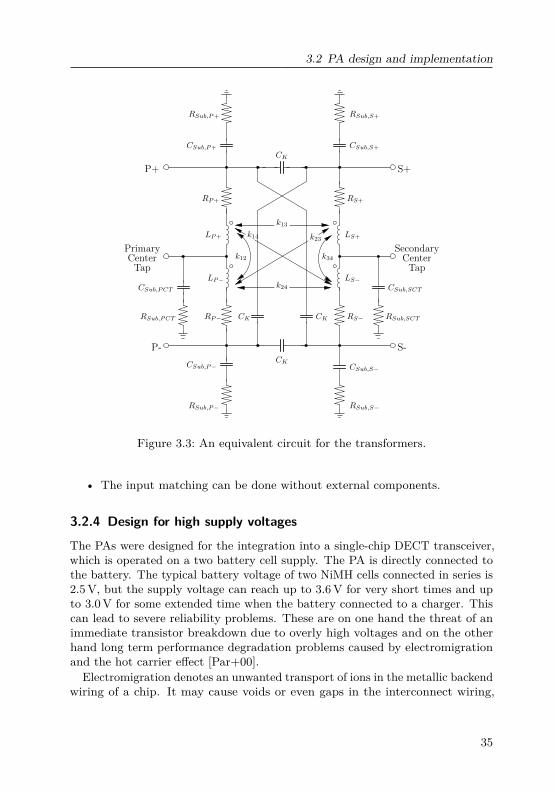
3.2 PA design and implementation
CSub,SCT
SecondaryCenterTap
RSub,SCT
S-
S+
RSub,P+ RSub,S+
P-
P+
PrimaryCenterTap
RSub,PCT
CSub,PCTk24
CK
k13
CK
CSub,P−
RSub,P−
CSub,P+
CK
RP+
LP+
RP−
LP−
LS+
RS−
LS−
CSub,S−
RSub,S−
RS+
CSub,S+
CK
k12 k34
k23k14
Figure 3.3: An equivalent circuit for the transformers.
• The input matching can be done without external components.
3.2.4 Design for high supply voltages
The PAs were designed for the integration into a single-chip DECT transceiver,which is operated on a two battery cell supply. The PA is directly connected tothe battery. The typical battery voltage of two NiMH cells connected in series is2.5V, but the supply voltage can reach up to 3.6V for very short times and upto 3.0V for some extended time when the battery connected to a charger. Thiscan lead to severe reliability problems. These are on one hand the threat of animmediate transistor breakdown due to overly high voltages and on the otherhand long term performance degradation problems caused by electromigrationand the hot carrier effect [Par+00].
Electromigration denotes an unwanted transport of ions in the metallic backendwiring of a chip. It may cause voids or even gaps in the interconnect wiring,
35
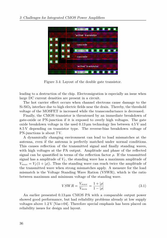
3 Challenges for Integrated CMOS Power Amplifiers
Figure 3.4: Layout of the double gate transistor.
leading to a destruction of the chip. Electromigration is especially an issue whenlarge DC current densities are present in a circuit.The hot carrier effect occurs when channel electrons cause damage to the
Si-SiO2 interface due to high electric fields near the drain. Thereby, the thresholdvoltage of the MOSFET is increased while the transconductance is decreased.
Finally, the CMOS transistor is threatened by an immediate breakdown ofgate-oxide or PN-junction if it is exposed to overly high voltages. The gateoxide breakdown voltage in the used 0.13µm technology lies between 4.5V and8.5V depending on transistor type. The reverse-bias breakdown voltage ofPN-junctions is about 7V.A dynamically changing environment can lead to load mismatches at the
antenna, even if the antenna is perfectly matched under normal conditions.This causes reflection of the transmitted signal and finally standing waves,with high voltages at the PA output. Amplitude and phase of the reflectedsignal can be quantified in terms of the reflection factor ρ. If the transmittedsignal has a amplitude of Vf , the standing wave has a maximum amplitude ofVmax = Vf (1 + |ρ|). Thus the standing wave can reach twice the amplitude ofthe transmitted wave when strong mismatches apply. A measure for the loadmismatch is the Voltage Standing Wave Ration (VSWR), which is the ratiobetween maximum and minimum voltage of the standing wave.
V SWR = VmaxVmin
= 1 + |ρ|1− |ρ| (3.1)
An earlier presented 0.13µm CMOS PA with a comparable output powershowed good performance, but had reliability problems already at low supplyvoltages above 1.2V [Vas+04]. Therefore special emphasis has been placed onreliability issues for design and layout.
36
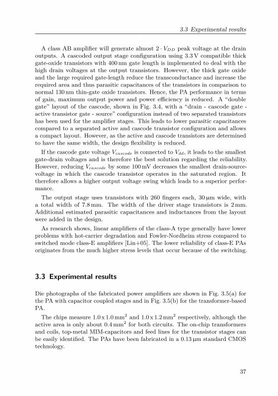
3.3 Experimental results
A class AB amplifier will generate almost 2 · VDD peak voltage at the drainoutputs. A cascoded output stage configuration using 3.3V compatible thickgate-oxide transistors with 400 nm gate length is implemented to deal with thehigh drain voltages at the output transistors. However, the thick gate oxideand the large required gate-length reduce the transconductance and increase therequired area and thus parasitic capacitances of the transistors in comparison tonormal 130 nm thin-gate oxide transistors. Hence, the PA performance in termsof gain, maximum output power and power efficiency is reduced. A “doublegate” layout of the cascode, shown in Fig. 3.4, with a “drain - cascode gate -active transistor gate - source” configuration instead of two separated transistorshas been used for the amplifier stages. This leads to lower parasitic capacitancescompared to a separated active and cascode transistor configuration and allowsa compact layout. However, as the active and cascode transistors are determinedto have the same width, the design flexibility is reduced.
If the cascode gate voltage Vcascode is connected to Vdd, it leads to the smallestgate-drain voltages and is therefore the best solution regarding the reliability.However, reducing Vcascode by some 100mV decreases the smallest drain-source-voltage in which the cascode transistor operates in the saturated region. Ittherefore allows a higher output voltage swing which leads to a superior perfor-mance.The output stage uses transistors with 260 fingers each, 30µm wide, with
a total width of 7.8mm. The width of the driver stage transistors is 2mm.Additional estimated parasitic capacitances and inductances from the layoutwere added in the design.
As research shows, linear amplifiers of the class-A type generally have lowerproblems with hot-carrier degradation and Fowler-Nordheim stress compared toswitched mode class-E amplifiers [Lin+05]. The lower reliability of class-E PAsoriginates from the much higher stress levels that occur because of the switching.
3.3 Experimental results
Die photographs of the fabricated power amplifiers are shown in Fig. 3.5(a) forthe PA with capacitor coupled stages and in Fig. 3.5(b) for the transformer-basedPA.
The chips measure 1.0 x 1.0mm2 and 1.0 x 1.2mm2 respectively, although theactive area is only about 0.4mm2 for both circuits. The on-chip transformersand coils, top-metal MIM-capacitors and feed lines for the transistor stages canbe easily identified. The PAs have been fabricated in a 0.13µm standard CMOStechnology.
37
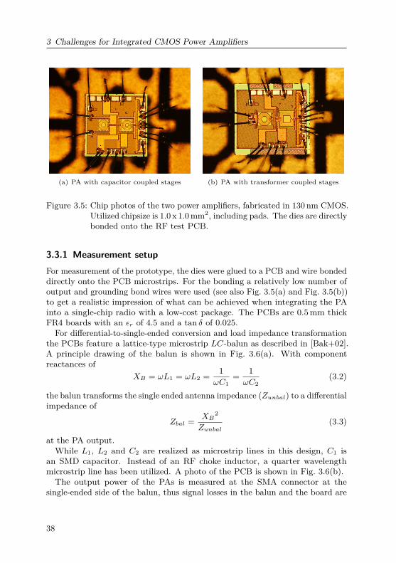
3 Challenges for Integrated CMOS Power Amplifiers
(a) PA with capacitor coupled stages (b) PA with transformer coupled stages
Figure 3.5: Chip photos of the two power amplifiers, fabricated in 130 nm CMOS.Utilized chipsize is 1.0 x 1.0mm2, including pads. The dies are directlybonded onto the RF test PCB.
3.3.1 Measurement setupFor measurement of the prototype, the dies were glued to a PCB and wire bondeddirectly onto the PCB microstrips. For the bonding a relatively low number ofoutput and grounding bond wires were used (see also Fig. 3.5(a) and Fig. 3.5(b))to get a realistic impression of what can be achieved when integrating the PAinto a single-chip radio with a low-cost package. The PCBs are 0.5mm thickFR4 boards with an εr of 4.5 and a tan δ of 0.025.
For differential-to-single-ended conversion and load impedance transformationthe PCBs feature a lattice-type microstrip LC-balun as described in [Bak+02].A principle drawing of the balun is shown in Fig. 3.6(a). With componentreactances of
XB = ωL1 = ωL2 = 1ωC1
= 1ωC2
(3.2)
the balun transforms the single ended antenna impedance (Zunbal) to a differentialimpedance of
Zbal = XB2
Zunbal(3.3)
at the PA output.While L1, L2 and C2 are realized as microstrip lines in this design, C1 is
an SMD capacitor. Instead of an RF choke inductor, a quarter wavelengthmicrostrip line has been utilized. A photo of the PCB is shown in Fig. 3.6(b).The output power of the PAs is measured at the SMA connector at the
single-ended side of the balun, thus signal losses in the balun and the board are
38
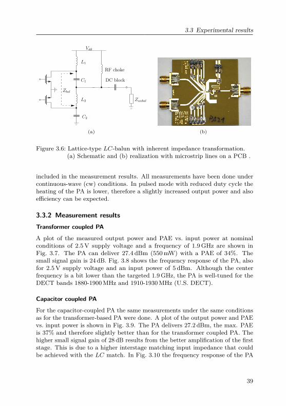
3.3 Experimental results
Zunbal
Vdd
L2
C1
L1
C2
DC block
RF choke
Zbal
(a) (b)
Figure 3.6: Lattice-type LC-balun with inherent impedance transformation.(a) Schematic and (b) realization with microstrip lines on a PCB .
included in the measurement results. All measurements have been done undercontinuous-wave (cw) conditions. In pulsed mode with reduced duty cycle theheating of the PA is lower, therefore a slightly increased output power and alsoefficiency can be expected.
3.3.2 Measurement resultsTransformer coupled PA
A plot of the measured output power and PAE vs. input power at nominalconditions of 2.5V supply voltage and a frequency of 1.9GHz are shown inFig. 3.7. The PA can deliver 27.4 dBm (550mW) with a PAE of 34%. Thesmall signal gain is 24 dB. Fig. 3.8 shows the frequency response of the PA, alsofor 2.5V supply voltage and an input power of 5 dBm. Although the centerfrequency is a bit lower than the targeted 1.9GHz, the PA is well-tuned for theDECT bands 1880-1900MHz and 1910-1930MHz (U.S. DECT).
Capacitor coupled PA
For the capacitor-coupled PA the same measurements under the same conditionsas for the transformer-based PA were done. A plot of the output power and PAEvs. input power is shown in Fig. 3.9. The PA delivers 27.2 dBm, the max. PAEis 37% and therefore slightly better than for the transformer coupled PA. Thehigher small signal gain of 28 dB results from the better amplification of the firststage. This is due to a higher interstage matching input impedance that couldbe achieved with the LC match. In Fig. 3.10 the frequency response of the PA
39
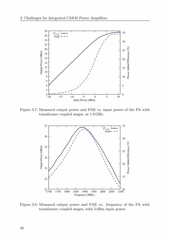
3 Challenges for Integrated CMOS Power Amplifiers
0 2 4 6 8
10 12 14 16 18 20 22 24 26 28
−20 −15 −10 −5 0 5 10 0
5
10
15
20
25
30
35
Out
put P
ower
[dBm
]
Pow
er A
dded
Effi
cien
cy [%
]
Input Power [dBm]
PAEPout
Figure 3.7: Measured output power and PAE vs. input power of the PA withtransformer coupled stages, at 1.9GHz.
21
22
23
24
25
26
27
1700 1750 1800 1850 1900 1950 2000 2050 2100 10
15
20
25
30
35
Out
put P
ower
[dBm
]
Pow
er A
dded
Effi
cien
cy [%
]
Frequency [MHz]
PAEPout
Figure 3.8: Measured output power and PAE vs. frequency of the PA withtransformer coupled stages, with 5 dBm input power.
40
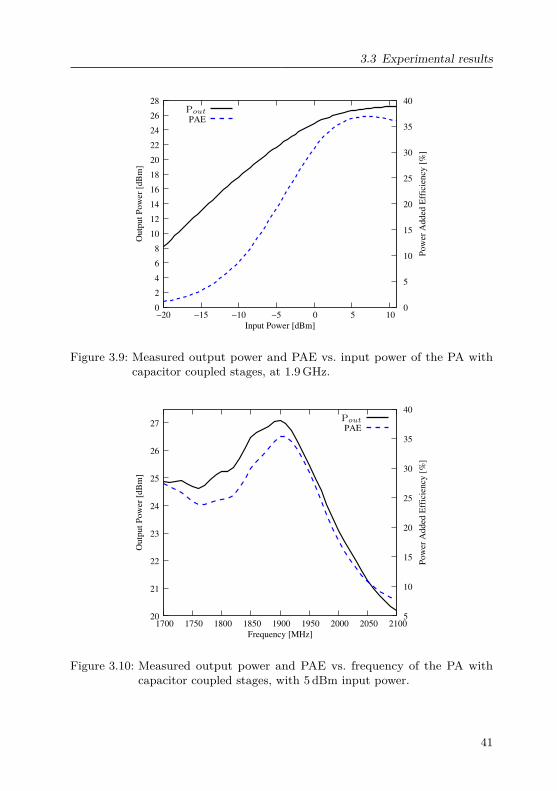
3.3 Experimental results
0 2 4 6 8
10 12 14 16 18 20 22 24 26 28
−20 −15 −10 −5 0 5 10 0
5
10
15
20
25
30
35
40
Out
put P
ower
[dBm
]
Pow
er A
dded
Effi
cien
cy [%
]
Input Power [dBm]
PAEPout
Figure 3.9: Measured output power and PAE vs. input power of the PA withcapacitor coupled stages, at 1.9GHz.
20
21
22
23
24
25
26
27
1700 1750 1800 1850 1900 1950 2000 2050 2100 5
10
15
20
25
30
35
40
Out
put P
ower
[dBm
]
Pow
er A
dded
Effi
cien
cy [%
]
Frequency [MHz]
PAEPout
Figure 3.10: Measured output power and PAE vs. frequency of the PA withcapacitor coupled stages, with 5 dBm input power.
41
3 Challenges for Integrated CMOS Power Amplifiers
is shown. It can be seen that the output power and PAE remain relatively highbelow the center frequency, but drop a bit faster for higher frequencies comparedto the transformer-based PA. This is caused by a shift of the center frequency inone of the two matching circuits.
Both PAs meet the requirements for DECT, which is 24 dBm transmit signalpower at the antenna, which translates to about 26 dBm at the PA output.
3.3.3 Reliability analysisThe RF performance of analog CMOS circuits can be degraded through thehot carrier effect. To evaluate the influence of the hot carrier effect, a longterm measurement of the hot carrier degradation has been accomplished withthe capacitor coupled PA and compared with [Vat+01], which shows an outputpower drop of 0.8 dB in only 80 hours of operation time. The PA was operatedat 3.6V supply voltage and biased to deliver 26.5 dBm of output power at 5 dBminput power. After 170 hours (7 days) of operation with 100% duty cycle, the PAshowed no output power performance degradation, which shows the robustnessof this PA design.
A ruggedness measurement has been conducted to test the sensitivity againstload mismatches with a resulting high VSWR. The supply voltage has beenraised in steps and an open or short condition has been applied at the SMAantenna connector. The supply voltage could be raised up to 6V until the PAoutput stage broke down! This shows that the topology of the output stagedescribed in section 3.2.4 gives a very good ruggedness against high supplyvoltages and VSWRs.
3.4 Active over-voltage protection circuits
The over-voltage protection, which has been discussed above, is grounded on theutilization of a high-voltage compliant thick-gateoxide transistors. Manufactur-ing of these devices necessitates additional process steps and therefore meansadditional costs. Also, RF performance of these transistors is generally inferior tostandard thin-gate oxide transistors. Finally, a lot of semiconductor companiesare “fabless” and manufacture at independent semiconductor foundries, makingit difficult to integrate special high-voltage transistors into the processes.Therefore, solving the issue on circuit level is a promising alternative. In
[Scu+05] a voltage feedback circuit to avoid overvoltages is presented. However,this circuit is only realizable with bipolar transistors, making it unsuitable forCMOS PAs.
In [Zim+08b] a VSWR protection circuit for CMOS PAs is presented. Criticallyhigh voltages at the PA’s open drain outputs are sensed by an overvoltagedetection circuit. If a critically high voltage is detected, it dynamically lowers
42
3.5 Conclusions and discussion of the results
biasing and gain of the amplifying stages, thereby immediately lowering theoutput voltage level back to an uncritical value.
3.5 Conclusions and discussion of the results
Two PAs intended for DECT applications were presented above. They both havean output power of more than +27 dBm and fulfill the DECT requirement. Usingthe presented results as a basis, a full integration of a similar power amplifier intoa true single-chip DECT telephone could be realized [Gre+07]. This shows that itis feasible to build CMOS power amplifiers with almost Watt-level output powersin standard CMOS technologies and integrate them with an RF transceiver andbaseband signal processing in one single chip.
3.5.1 Feasibility of single-chip radios with integrated CMOS PA forcellular standards
Subsequently, the technological limits and challenges of a PA integration intoa single-chip transceiver for different communication standards are discussed.It shall be concluded for which kind of communication system, besides DECT,such a PA integration is feasible and for which it is not, assuming the utilizationof state-of-the-art CMOS technology.
In literature, CMOS PAs with even higher peak output power than the abovepresented PAs with levels up to +35 dBm can be found [Cho+09; Aok+08].To achieve this, their architecture is based on the power combination of Nparallel PAs through a transformer, where the secondary (output) coils of Ntransformers are connected in series and their primary (input) coils are connectedin parallel. This has got especially popular with the invention of the so-called“distributed active transformer” (DAT) by Aoki et al. [Aok+02], where thetransformer is constructed out of “slab” inductors. To be able to build a low-lossintegrated power combination network, however, a special chip backend withvery thick metal layers is needed. This, of course, means increased productioncosts compared to standard CMOS solutions with a conventional wiring backend.Therefore, it is not compatible with the idea of building a fully integrated low-costsingle-chip radio in digital-centric nanoscale standard CMOS.Looking at the output power levels measured in section 3.3.2, it can be seen
that peak output power levels of around 500mW (+27dBm) are feasible withstandard CMOS. With power-combination techniques like the DAT even outputlevels above +30 dB are possible. However, these are always peak power levelswhere the PA is operated in strong compression. The peak output power onlyequals the defined maximum average power level for modulation schemes witha constant signal envelope. This is the case for communication standards like
43
3 Challenges for Integrated CMOS Power Amplifiers
DECT or GSM, which both have a GMSK modulation scheme.1 For high-data-rate communication standards with envelope varying amplitude modulationschemes such as WLAN, WCDMA (UMTS) or LTE, however, a linear poweramplifier is needed.2 If the communication standard demands a linear signalamplification, it can be seen from the measurements in Fig. 3.7 and Fig. 3.9 thata maximum uncompressed output power of around +24dBm can be reached.The average output power level is even below this level. It is reduced by thepeak to average power ratio (PAPR) of the utilized modulation scheme. QAMmodulation schemes that are used for WCDMA and HSPA have a PAPR of 3to 7 dB (depending on the modulation order). OFDM modulation schemes asdiscussed in section 2.4.3 for WLAN and LTE even have higher PAPRs of 11 to17 dB [McC10, pp. 392–400].
Connectivity devices such as WLAN and Bluetooth (BT) have relativelylow output power levels which are significantly below +20 dBm. WLAN IEEE802.11x defines a maximum EIRP of +20 dBm, BT class 1 devices – which arethe devices with the highest output power defined for BT – also have a maximumoutput power of +20 dBm. Because of the antenna gain which has to be takeninto account for EIRP, the maximum average PA output power is some dB lower.High-data-rate cellular standards, on the other hand, require a much higher
(average) output power. UMTS, for example, has a defined maximum averageoutput power of +24 dBm and LTE has maximum average output power of+23 dBm.
Therefore, single chip solutions with integrated power amplifiers today canonly be found for wireless connectivity radios such as WLAN or Bluetooth[Lee+10; Afs+09; Beh+07]. The 1 dB compression point of these devices is farbelow +20dBm. The fully integrated device with the highest reported outputpower is the DECT chip of Grewing et al. [Gre+07] with an output powerof +26 dBm. The constant envelope modulation scheme of DECT, however,allows to operate the PA in saturation. From the discussion above, it can beconcluded that it is unfeasible – or at least very hard – to build a fully integratedsingle-chip transceiver in today’s low-cost standard CMOS for high-data-ratecellular standards such as LTE or WCDMA (HSUPA).
1Where DECT has a defined maximum output power of +24 dBm at the antenna and GSMhas a much higher maximum output power of +33 dBm.
2Unless a polar modulator architecture or LINC is used, which, on the other hand, limitsthe usable signal bandwidth as discussed in sections 2.3.2 and 5.4.1.
44
4 RF-DAC Fundamentals
Scope of this work is to develop a transmitter architecture, which is compatiblewith modern broadband high-data-rate communication standards. At the sametime it must be cost efficient as it is targeted on the highly competitive mobilecommunications consumer market.
To achieve low production costs at high quantities of sold units, the transmittermust be highly integrated in a nanoscale CMOS process. Thereby, the numberof bulky and expensive external components as well as the production cost ofthe transceiver chip can be minimized. Nanoscale CMOS processes are perfectlysuited for digital circuits as they allow high processing speed at a low power andarea consumption. However, the analog performance – besides a high transitfrequency ft of the transistors – of these technologies increasingly worsens withdecreasing feature size. This is mainly due to the low supply voltages that maybe applied to nanoscale CMOS transistors which have a gate oxide thickness inthe low single-digit nanometer range. Also, the analog performance suffers fromshort-channel transistor effects. Therefore, novel circuit implementations andsystem architectures have to be found that allow to cope with a relatively pooranalog transistor performance.
A second challenge for the development of a low-cost reconfigurable transmitterare the high performance requirements of novel high-data-rate OFDM-basedcommunication standards such as LTE and WLAN. Still, legacy standards asGSM and UMTS have to be supported, as these will most likely be present formany years to come. To limit the hardware cost and the size of a multistandardcommunication device like a smartphone, the transmitter should be highlyreconfigurable, thereby being able to service different radio standards with thesame hardware. This demands a reconfigurable high-performance analog andRF frontend which is able to fulfill the different performance requirements of allsupported radio standards.As discussed in the previous chapter, it is not feasible with state-of-the art
technology to integrate a power amplifier into a single-chip radio which is capableto deliver the high output power that is needed for cellular standards. Thus, asolution which consists of a fully integrated, flexible, low-cost modulator plus anexternal PA has to be found.
Subsequently, different possible solutions for multistandard, multimode trans-mitters are discussed. These have to be as “digital” as possible. By replacingthe analog baseband processing with digital blocks, the transmitter can be made
45
4 RF-DAC Fundamentals
highly reconfigurable. The most promising approach for such a “direct-digital”transmitter is the RF-DAC. Different earlier published RF-DAC implementa-tions are presented. Also, drawbacks of RF-DAC based transmitters, namelyunwanted spurious emissions, are discussed and techniques to reduce theseunwanted emissions are introduced.
4.1 Basic idea of the RF-DAC transmitter
In recent years, several ideas for building reconfigurable, “direct-digital” trans-mitters have been published [Elo+07; JS07; Tal+08]. They are based on thedirect conversion of a digital baseband signal into an analog RF output signal,by using a building block which combines D/A conversion and upconversionmixing. The first implementations of this technique were introduced by Zhouand Yuan [ZY02] and Luschas et al. [Lus+04]. The digital-to-RF converter wastermed “RF-DAC”. It seems to be an excellent alternative to classical analogtransmitter architectures which have been used for many decades.
4.1.1 Current-steering DACsThe idea of all RF-DAC structures originates in a conventional current-steeringDAC [Raz95, p. 84 ff.]. The working principle of a current steering DAC isshown in Fig. 4.1. It consists of a number of parallel switched current sources,the DAC unit cells. Each unit cell is built by a weighted fixed current sourceand a switching pair, which steers the current to either the output or dumpsit to ground, depending on the digital input data. Alternatively to dumpingthe current to ground, a current steering between two differential outputs Iout+or Iout− is also possible. The weighted currents of all parallel unit cells aresummed at the output and converted into a voltage by a transimpedance stage,if necessary. This D/A converter structure is especially popular for high-speedapplications as it can directly drive a resistive load. No high-speed amplifier isneeded at the output and hence current steering DACs are potentially fasterthan other DAC topologies.
The simplest construction of a N bit current-steering DAC is an architecturewith N parallel binary weighted current sources as depicted in Fig. 4.1. Thisarchitecture, however, suffers from two drawbacks:First, device matching problems can lead to nonlinearities and even a non-
monotonic behavior in the output current when switching from one output valueto the next. This is especially an issue when switching from a value 2n− 1 to 2n,where all currently active current sources (I0 to In−1) have to be switched offand the next larger source In is switched on. Performance metrics for measuringthese nonlinear effects are the differential nonlinearity (DNL), which is themaximum deviation in the output step size from the ideal value of one least
46
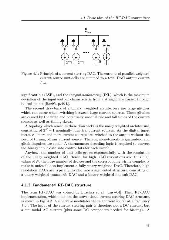
4.1 Basic idea of the RF-DAC transmitter
2N-1I 2
N-2I 2I I
Iout
Figure 4.1: Principle of a current steering DAC. The currents of parallel, weightedcurrent source unit-cells are summed to a total DAC output currentIout.
significant bit (LSB), and the integral nonlinearity (INL), which is the maximumdeviation of the input/output characteristic from a straight line passed throughits end points [Raz95, p.48 f.].The second drawback of a binary weighted architecture are large glitches
which can occur when switching between large current sources. These glitchesare caused by the finite and potentially unequal rise and fall times of the currentsources as well as timing skews.
A topology which remedies these drawbacks is the unary weighted architecture,consisting of 2N − 1 nominally identical current sources. As the digital inputincreases, more and more current sources are switched to the output without theneed of turning off any current source. Thereby, monotonicity is guaranteed andglitch impulses are small. A thermometer decoding logic is required to convertthe binary input data into control bits for each switch.Anyhow, the number of unit cells grows exponentially with the resolution
of the unary weighted DAC. Hence, for high DAC resolutions and thus highvalues of N , the huge number of devices and the corresponding wiring complexitymake it unfeasible to implement a fully unary weighted DAC. Therefore, highresolution DACs are typically divided into a segmented structure, consisting ofa unary weighted coarse sub-DAC and a binary weighted fine sub-DAC.
4.1.2 Fundamental RF-DAC structure
The term RF-DAC was coined by Luschas et al. [Lus+04]. Their RF-DACimplementation, which modifies the conventional current-steering DAC structure,is shown in Fig. 4.2. A sine wave modulates the tail current source at a frequencyfLO. The input of the current-steering pair is therefore not a DC current, buta sinusoidal AC current (plus some DC component needed for biasing). A
47
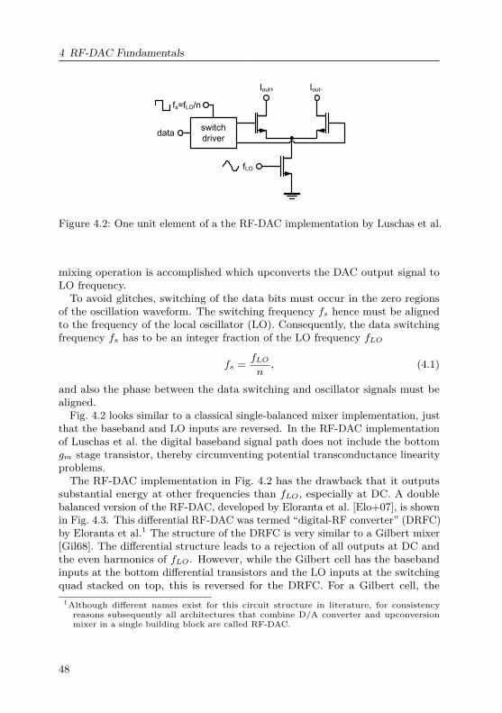
4 RF-DAC Fundamentals
switch
driverdata
fs=fLO/n
fLO
Iout+ Iout-
Figure 4.2: One unit element of a the RF-DAC implementation by Luschas et al.
mixing operation is accomplished which upconverts the DAC output signal toLO frequency.To avoid glitches, switching of the data bits must occur in the zero regions
of the oscillation waveform. The switching frequency fs hence must be alignedto the frequency of the local oscillator (LO). Consequently, the data switchingfrequency fs has to be an integer fraction of the LO frequency fLO
fs = fLOn, (4.1)
and also the phase between the data switching and oscillator signals must bealigned.
Fig. 4.2 looks similar to a classical single-balanced mixer implementation, justthat the baseband and LO inputs are reversed. In the RF-DAC implementationof Luschas et al. the digital baseband signal path does not include the bottomgm stage transistor, thereby circumventing potential transconductance linearityproblems.The RF-DAC implementation in Fig. 4.2 has the drawback that it outputs
substantial energy at other frequencies than fLO, especially at DC. A doublebalanced version of the RF-DAC, developed by Eloranta et al. [Elo+07], is shownin Fig. 4.3. This differential RF-DAC was termed “digital-RF converter” (DRFC)by Eloranta et al.1 The structure of the DRFC is very similar to a Gilbert mixer[Gil68]. The differential structure leads to a rejection of all outputs at DC andthe even harmonics of fLO. However, while the Gilbert cell has the basebandinputs at the bottom differential transistors and the LO inputs at the switchingquad stacked on top, this is reversed for the DRFC. For a Gilbert cell, the
1Although different names exist for this circuit structure in literature, for consistencyreasons subsequently all architectures that combine D/A converter and upconversionmixer in a single building block are called RF-DAC.
48
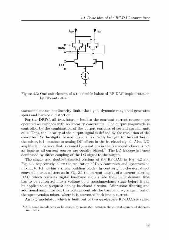
4.1 Basic idea of the RF-DAC transmitter
data
Iout+ Iout-
LO
Figure 4.3: One unit element of a the double balanced RF-DAC implementationby Eloranta et al.
transconductance nonlinearity limits the signal dynamic range and generatesspurs and harmonic distortion.For the DRFC, all transistors – besides the constant current source – are
operated as switches with no linearity constraints. The output magnitude iscontrolled by the combination of the output currents of several parallel unitcells. Thus, the linearity of the output signal is defined by the resolution of theconverter. As the digital baseband signal is directly brought to the switches ofthe mixer, it is immune to analog DC-offsets in the baseband signal. Also, I/Qamplitude imbalance that is caused by variations in the transconductance is notan issue as all current sources are equally biased.2 The LO leakage is hencedominated by direct coupling of the LO signal to the output.The single- and double-balanced versions of the RF-DAC in Fig. 4.2 and
Fig. 4.3, respectively, allow the realization of D/A conversion and upconversionmixing to RF within a single building block. In contrast, for classical directconversion transmitters as in Fig. 2.1 the current output of a current-steeringDAC, which converts digital baseband signals into the analog domain, firsthas to be converted into a voltage by a transimpedance stage before it canbe applied to subsequent analog baseband circuits. After some filtering andadditional amplification, this voltage controls the baseband gm stage input ofthe upconversion mixer, where it is converted back into a current.An I/Q modulator which is built out of two quadrature RF-DACs is called
2Still, some imbalance can be caused by mismatch between the current sources of differentunit cells.
49
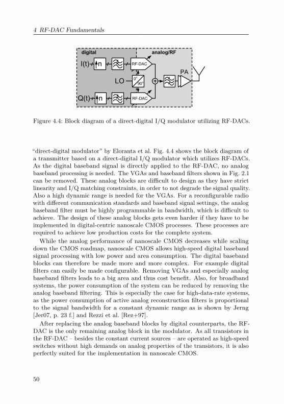
4 RF-DAC Fundamentals
digital
I(t)
Q(t)
LO 0o
90o
n
RF-DACn
RF-DAC
PA
analog/RF
Figure 4.4: Block diagram of a direct-digital I/Q modulator utilizing RF-DACs.
“direct-digital modulator” by Eloranta et al. Fig. 4.4 shows the block diagram ofa transmitter based on a direct-digital I/Q modulator which utilizes RF-DACs.As the digital baseband signal is directly applied to the RF-DAC, no analogbaseband processing is needed. The VGAs and baseband filters shown in Fig. 2.1can be removed. These analog blocks are difficult to design as they have strictlinearity and I/Q matching constraints, in order to not degrade the signal quality.Also a high dynamic range is needed for the VGAs. For a reconfigurable radiowith different communication standards and baseband signal settings, the analogbaseband filter must be highly programmable in bandwidth, which is difficult toachieve. The design of these analog blocks gets even harder if they have to beimplemented in digital-centric nanoscale CMOS processes. These processes arerequired to achieve low production costs for the complete system.While the analog performance of nanoscale CMOS decreases while scaling
down the CMOS roadmap, nanoscale CMOS allows high-speed digital basebandsignal processing with low power and area consumption. The digital basebandblocks can therefore be made more and more complex. For example digitalfilters can easily be made configurable. Removing VGAs and especially analogbaseband filters leads to a big area and thus cost benefit. Also, for broadbandsystems, the power consumption of the system can be reduced by removing theanalog baseband filtering. This is especially the case for high-data-rate systems,as the power consumption of active analog reconstruction filters is proportionalto the signal bandwidth for a constant dynamic range as is shown by Jerng[Jer07, p. 23 f.] and Rezzi et al. [Rez+97].After replacing the analog baseband blocks by digital counterparts, the RF-
DAC is the only remaining analog block in the modulator. As all transistors inthe RF-DAC – besides the constant current sources – are operated as high-speedswitches without high demands on analog properties of the transistors, it is alsoperfectly suited for the implementation in nanoscale CMOS.
50
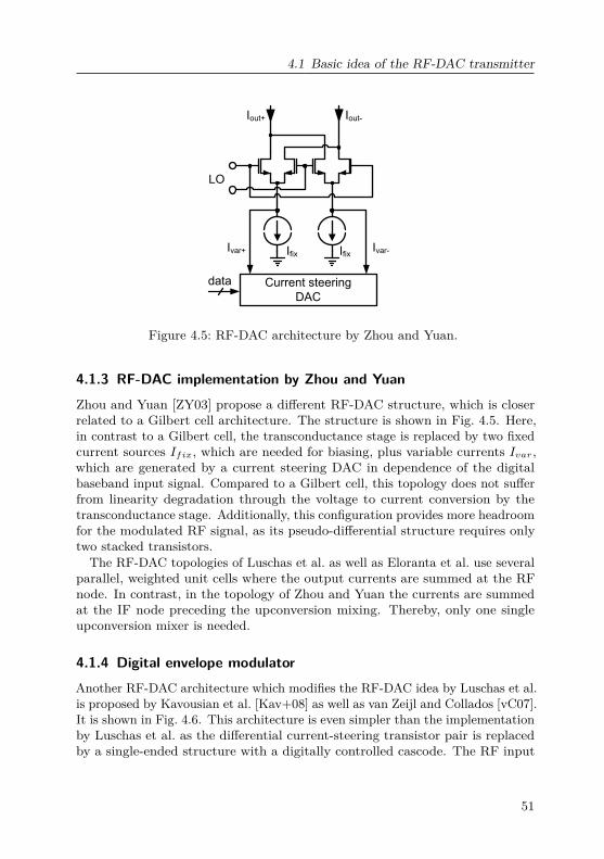
4.1 Basic idea of the RF-DAC transmitter
Iout+ Iout-
LO
Current steering
DAC
Ivar+ Ivar-Ifix Ifix
data
Figure 4.5: RF-DAC architecture by Zhou and Yuan.
4.1.3 RF-DAC implementation by Zhou and YuanZhou and Yuan [ZY03] propose a different RF-DAC structure, which is closerrelated to a Gilbert cell architecture. The structure is shown in Fig. 4.5. Here,in contrast to a Gilbert cell, the transconductance stage is replaced by two fixedcurrent sources Ifix, which are needed for biasing, plus variable currents Ivar,which are generated by a current steering DAC in dependence of the digitalbaseband input signal. Compared to a Gilbert cell, this topology does not sufferfrom linearity degradation through the voltage to current conversion by thetransconductance stage. Additionally, this configuration provides more headroomfor the modulated RF signal, as its pseudo-differential structure requires onlytwo stacked transistors.
The RF-DAC topologies of Luschas et al. as well as Eloranta et al. use severalparallel, weighted unit cells where the output currents are summed at the RFnode. In contrast, in the topology of Zhou and Yuan the currents are summedat the IF node preceding the upconversion mixing. Thereby, only one singleupconversion mixer is needed.
4.1.4 Digital envelope modulatorAnother RF-DAC architecture which modifies the RF-DAC idea by Luschas et al.is proposed by Kavousian et al. [Kav+08] as well as van Zeijl and Collados [vC07].It is shown in Fig. 4.6. This architecture is even simpler than the implementationby Luschas et al. as the differential current-steering transistor pair is replacedby a single-ended structure with a digitally controlled cascode. The RF input
51
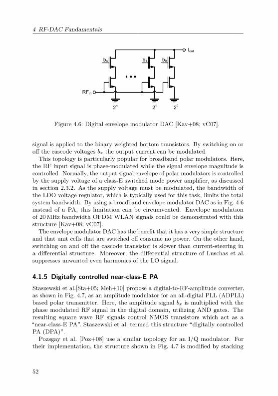
4 RF-DAC Fundamentals
20
21
2n
RFin
Iout
bn b1 b0
Figure 4.6: Digital envelope modulator DAC [Kav+08; vC07].
signal is applied to the binary weighted bottom transistors. By switching on oroff the cascode voltages bx the output current can be modulated.This topology is particularly popular for broadband polar modulators. Here,
the RF input signal is phase-modulated while the signal envelope magnitude iscontrolled. Normally, the output signal envelope of polar modulators is controlledby the supply voltage of a class-E switched mode power amplifier, as discussedin section 2.3.2. As the supply voltage must be modulated, the bandwidth ofthe LDO voltage regulator, which is typically used for this task, limits the totalsystem bandwidth. By using a broadband envelope modulator DAC as in Fig. 4.6instead of a PA, this limitation can be circumvented. Envelope modulationof 20MHz bandwidth OFDM WLAN signals could be demonstrated with thisstructure [Kav+08; vC07].
The envelope modulator DAC has the benefit that it has a very simple structureand that unit cells that are switched off consume no power. On the other hand,switching on and off the cascode transistor is slower than current-steering ina differential structure. Moreover, the differential structure of Luschas et al.suppresses unwanted even harmonics of the LO signal.
4.1.5 Digitally controlled near-class-E PAStaszewski et al.[Sta+05; Meh+10] propose a digital-to-RF-amplitude converter,as shown in Fig. 4.7, as an amplitude modulator for an all-digital PLL (ADPLL)based polar transmitter. Here, the amplitude signal bx is multiplied with thephase modulated RF signal in the digital domain, utilizing AND gates. Theresulting square wave RF signals control NMOS transistors which act as a“near-class-E PA”. Staszewski et al. termed this structure “digitally controlledPA (DPA)”.Pozsgay et al. [Poz+08] use a similar topology for an I/Q modulator. For
their implementation, the structure shown in Fig. 4.7 is modified by stacking
52
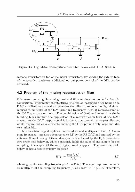
4.2 Problem of the missing reconstruction filter
20
21
2n
RFin
Iout
bn b1 b0
RFin
bx
Figure 4.7: Digital-to-RF-amplitude converter, near-class-E DPA [Sta+05].
cascode transistors on top of the switch transistors. By varying the gate voltageof the cascode transistors, additional output power control of the DPA can beachieved.
4.2 Problem of the missing reconstruction filter
Of course, removing the analog baseband filtering does not come for free. Inconventional transmitter architectures, the analog baseband filter behind theDAC is utilized as a so-called reconstruction filter to remove the digital signalreplicas at multiples of the DAC sampling frequency. Also, it removes some ofthe DAC quantization noise. The combination of DAC and mixer in a singlebuilding block inhibits the application of a reconstruction filter at the DACoutput. As the DAC output signal is in the current domain, a lowpass filteringwould require inductive elements, making the filter prohibitively large and alsovery inflexible.
Thus, baseband signal replicas – centered around multiples of the DAC sam-pling frequency – are also upconverted to RF by the RF-DAC and emitted by theantenna. Some filtering of these alias spectra is achieved by the D/A converter’szero order hold behavior, which constantly holds the value of one sample for onesampling time-step until the next digital word is applied. The zero order holdbehavior has a sinc frequency response
H(f) = sin(f/fs)f/fs
, (4.2)
where fs is the sampling frequency of the DAC. The sinc response has nullsat multiples of the sampling frequency fs as shown in Fig. 4.8. Therefore,
53
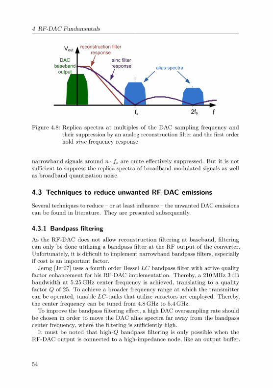
4 RF-DAC Fundamentals
Vout
ffs 2fs
reconstruction filter
response
alias spectra
DAC
baseband
output
sinc filter
response
Figure 4.8: Replica spectra at multiples of the DAC sampling frequency andtheir suppression by an analog reconstruction filter and the first orderhold sinc frequency response.
narrowband signals around n · fs are quite effectively suppressed. But it is notsufficient to suppress the replica spectra of broadband modulated signals as wellas broadband quantization noise.
4.3 Techniques to reduce unwanted RF-DAC emissions
Several techniques to reduce – or at least influence – the unwanted DAC emissionscan be found in literature. They are presented subsequently.
4.3.1 Bandpass filteringAs the RF-DAC does not allow reconstruction filtering at baseband, filteringcan only be done utilizing a bandpass filter at the RF output of the converter.Unfortunately, it is difficult to implement narrowband bandpass filters, especiallyif cost is an important factor.
Jerng [Jer07] uses a fourth order Bessel LC bandpass filter with active qualityfactor enhancement for his RF-DAC implementation. Thereby, a 210MHz 3 dBbandwidth at 5.25GHz center frequency is achieved, translating to a qualityfactor Q of 25. To achieve a broader frequency range at which the transmittercan be operated, tunable LC-tanks that utilize varactors are employed. Thereby,the center frequency can be tuned from 4.8GHz to 5.4GHz.
To improve the bandpass filtering effect, a high DAC oversampling rate shouldbe chosen in order to move the DAC alias spectra far away from the bandpasscenter frequency, where the filtering is sufficiently high.It must be noted that high-Q bandpass filtering is only possible when the
RF-DAC output is connected to a high-impedance node, like an output buffer.
54
4.3 Techniques to reduce unwanted RF-DAC emissions
In this case, an analog, linear on-chip amplifier is still required. If, on the otherhand, the RFout node is directly connected to an off-chip component like anexternal power amplifier, the overall quality factor is limited by the 50Ω systemimpedance that acts as a shunt resistance to the LC tank. Thereby, the Q andthus the effectiveness of the bandpass filter is reduced. Consequently, Elorantaand Seppinen [ES05] use an LC tank at the output node mainly as an outputmatching circuit. Their LC tank is designed to have an especially low qualityfactor as to allow wideband operation from 100MHz to 2.6GHz.
4.3.2 Influence of DAC resolution and oversamplingIn addition to the signal replicas at multiples of the sampling frequency, theDAC also emits unwanted broadband quantization noise. Quantization noisefor most practical purposes can be assumed to be uniformly distributed. Thus,a constant “noise floor” is perceived when measuring the quantization noisedensity vs. frequency. The overall quantization noise obviously decreases withan increase in converter resolution.
The maximum signal to noise ratio (SNR) of a DAC operated at Nyquist ratefor a sinusoidal input signal can be expressed as [Pla03, p. 9ff.]
SNRmax = 2N√
62 (4.3)
where N is the number of bits of the converter. Often, the SNR is given in termsof decibels (dB). Rewriting equation (4.3) in dB yields
SNRmax = 20 log102N ·√
62 = 6.02N dB + 1.76 dB. (4.4)
Hence, the quantization noise drops by approximately 6 dB for every additionalbit of resolution. It must be noted, however, that the effective resolution of aconverter is limited by nonlinearities and matching of the analog components.An effective number of bits (ENOB) of a Nyquist rate converter can be definedfrom an actual measured SNR by rearranging equation (4.4) [AH02, p. 617]
ENOB = SNRactual − 1.76 dB6.02 dB . (4.5)
Sampling at a higher frequency than the Nyquist frequency is called “oversam-pling”. By increasing the sampling rate, the quantization noise is randomizedover a larger frequency band. Thus, the quantization noise in the signal frequencyband decreases accordingly. This can be written as [Pla03]
SNRmax = 2n−1√3√
fsfsig
(4.6)
55
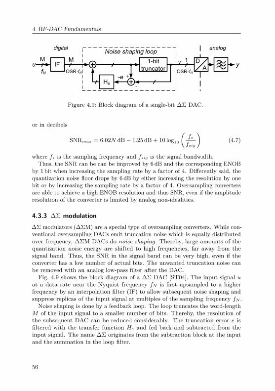
4 RF-DAC Fundamentals
DA
1-bit
truncatorIF
He
yfN
M
+
-
-e
Noise shaping loop
M
OSR·fN
1
OSR·fN
analog
u
digital
v
Figure 4.9: Block diagram of a single-bit ∆Σ DAC.
or in decibels
SNRmax = 6.02N dB− 1.25dB + 10 log10
(fsfsig
)(4.7)
where fs is the sampling frequency and fsig is the signal bandwidth.Thus, the SNR can be can be improved by 6 dB and the corresponding ENOB
by 1 bit when increasing the sampling rate by a factor of 4. Differently said, thequantization noise floor drops by 6 dB by either increasing the resolution by onebit or by increasing the sampling rate by a factor of 4. Oversampling convertersare able to achieve a high ENOB resolution and thus SNR, even if the amplituderesolution of the converter is limited by analog non-idealities.
4.3.3 ∆Σ modulation∆Σ modulators (∆ΣM) are a special type of oversampling converters. While con-ventional oversampling DACs emit truncation noise which is equally distributedover frequency, ∆ΣM DACs do noise shaping. Thereby, large amounts of thequantization noise energy are shifted to high frequencies, far away from thesignal band. Thus, the SNR in the signal band can be very high, even if theconverter has a low number of actual bits. The unwanted truncation noise canbe removed with an analog low-pass filter after the DAC.Fig. 4.9 shows the block diagram of a ∆Σ DAC [ST04]. The input signal u
at a data rate near the Nyquist frequency fN is first upsampled to a higherfrequency by an interpolation filter (IF) to allow subsequent noise shaping andsuppress replicas of the input signal at multiples of the sampling frequency fN .
Noise shaping is done by a feedback loop. The loop truncates the word-lengthM of the input signal to a smaller number of bits. Thereby, the resolution ofthe subsequent DAC can be reduced considerably. The truncation error e isfiltered with the transfer function He and fed back and subtracted from theinput signal. The name ∆Σ originates from the subtraction block at the inputand the summation in the loop filter.
56
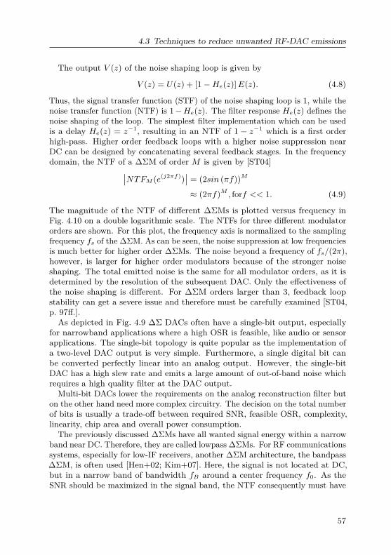
4.3 Techniques to reduce unwanted RF-DAC emissions
The output V (z) of the noise shaping loop is given by
V (z) = U(z) + [1−He(z)]E(z). (4.8)
Thus, the signal transfer function (STF) of the noise shaping loop is 1, while thenoise transfer function (NTF) is 1−He(z). The filter response He(z) defines thenoise shaping of the loop. The simplest filter implementation which can be usedis a delay He(z) = z−1, resulting in an NTF of 1 − z−1 which is a first orderhigh-pass. Higher order feedback loops with a higher noise suppression nearDC can be designed by concatenating several feedback stages. In the frequencydomain, the NTF of a ∆ΣM of order M is given by [ST04]∣∣NTFM (e(j2πf))
∣∣ = (2sin (πf))M
≈ (2πf)M , forf << 1. (4.9)
The magnitude of the NTF of different ∆ΣMs is plotted versus frequency inFig. 4.10 on a double logarithmic scale. The NTFs for three different modulatororders are shown. For this plot, the frequency axis is normalized to the samplingfrequency fs of the ∆ΣM. As can be seen, the noise suppression at low frequenciesis much better for higher order ∆ΣMs. The noise beyond a frequency of fs/(2π),however, is larger for higher order modulators because of the stronger noiseshaping. The total emitted noise is the same for all modulator orders, as it isdetermined by the resolution of the subsequent DAC. Only the effectiveness ofthe noise shaping is different. For ∆ΣM orders larger than 3, feedback loopstability can get a severe issue and therefore must be carefully examined [ST04,p. 97ff.].As depicted in Fig. 4.9 ∆Σ DACs often have a single-bit output, especially
for narrowband applications where a high OSR is feasible, like audio or sensorapplications. The single-bit topology is quite popular as the implementation ofa two-level DAC output is very simple. Furthermore, a single digital bit canbe converted perfectly linear into an analog output. However, the single-bitDAC has a high slew rate and emits a large amount of out-of-band noise whichrequires a high quality filter at the DAC output.
Multi-bit DACs lower the requirements on the analog reconstruction filter buton the other hand need more complex circuitry. The decision on the total numberof bits is usually a trade-off between required SNR, feasible OSR, complexity,linearity, chip area and overall power consumption.
The previously discussed ∆ΣMs have all wanted signal energy within a narrowband near DC. Therefore, they are called lowpass ∆ΣMs. For RF communicationssystems, especially for low-IF receivers, another ∆ΣM architecture, the bandpass∆ΣM, is often used [Hen+02; Kim+07]. Here, the signal is not located at DC,but in a narrow band of bandwidth fB around a center frequency f0. As theSNR should be maximized in the signal band, the NTF consequently must have
57
4 RF-DAC Fundamentals
10−3
10−2
10−1
−160
−140
−120
−100
−80
−60
−40
−20
0
20
Normalized Frequency
|NT
F| [d
B]
1st order
2nd order
3rd order
Figure 4.10: ∆ΣM NTF over normalized frequency in dependence of the modu-lator order.
a bandstop characteristic with zeros around f0. Bandpass NTFs can be derivedfrom an equivalent lowpass NTF by a so-called N-path transformation [ST04, p.145ff.].
Single-bit ∆Σ modulators in RF-transmitters
Recently, the utilization of single bit ∆ΣMs in RF transmitters has got anincreasingly popular research topic. A single-bit digital output allows to directlyuse a switching-mode PA as DAC with high power output, making the transmitterespecially simple and due to the utilization of a switching-mode PA potentiallyenergy efficient. Single-bit ∆ΣM transmitters use either a low-pass ∆ΣM withsubsequent digital upconversion mixer [Fra+09; Hel+08], or directly generatea ∆Σ modulated RF signal, using a bandpass ∆ΣM [Som+04]. However, thePA must be switched at several times the frequency of the RF carrier to achievea reasonable OSR. Also, the digital signal processing must run at these highfrequencies. This is hardly feasible with today‘s technology, especially if powerconsumption is a limiting factor. The combination of a low OSR and a single-bitDAC limits the achievable SNR. The required high-quality bandpass filters atthe RF output that are needed to suppress the unwanted truncation noise arebulky and very expensive. Therefore, single-bit ∆ΣM transmitters probably willnot get a commercially attractive alternative architecture in the near future,especially for mobile devices. Furthermore, as a large amount of the transmitted
58
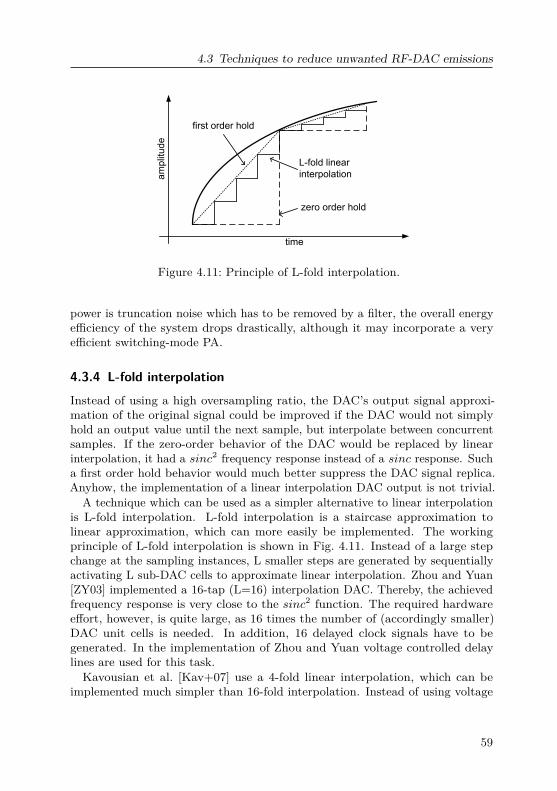
4.3 Techniques to reduce unwanted RF-DAC emissions
zero order hold
first order hold
L-fold linear
interpolation
time
am
plit
ud
e
Figure 4.11: Principle of L-fold interpolation.
power is truncation noise which has to be removed by a filter, the overall energyefficiency of the system drops drastically, although it may incorporate a veryefficient switching-mode PA.
4.3.4 L-fold interpolation
Instead of using a high oversampling ratio, the DAC’s output signal approxi-mation of the original signal could be improved if the DAC would not simplyhold an output value until the next sample, but interpolate between concurrentsamples. If the zero-order behavior of the DAC would be replaced by linearinterpolation, it had a sinc2 frequency response instead of a sinc response. Sucha first order hold behavior would much better suppress the DAC signal replica.Anyhow, the implementation of a linear interpolation DAC output is not trivial.
A technique which can be used as a simpler alternative to linear interpolationis L-fold interpolation. L-fold interpolation is a staircase approximation tolinear approximation, which can more easily be implemented. The workingprinciple of L-fold interpolation is shown in Fig. 4.11. Instead of a large stepchange at the sampling instances, L smaller steps are generated by sequentiallyactivating L sub-DAC cells to approximate linear interpolation. Zhou and Yuan[ZY03] implemented a 16-tap (L=16) interpolation DAC. Thereby, the achievedfrequency response is very close to the sinc2 function. The required hardwareeffort, however, is quite large, as 16 times the number of (accordingly smaller)DAC unit cells is needed. In addition, 16 delayed clock signals have to begenerated. In the implementation of Zhou and Yuan voltage controlled delaylines are used for this task.Kavousian et al. [Kav+07] use a 4-fold linear interpolation, which can be
implemented much simpler than 16-fold interpolation. Instead of using voltage
59
4 RF-DAC Fundamentals
controlled delay lines, simple frequency dividers can be utilized to generate theneeded quadrature clock signals.
4.3.5 Semidigital FIR filterAnother technique to suppress unwanted emissions is embedding a semi-digitalfinite impulse response (FIR) reconstruction filter in the digital-RF interface.Taleie et al. [Tal+08] use the 1-bit output of a ∆ΣM whose output goes througha 6-tap digital delay line. Each output of the delay line is applied to the inputof an RF-DAC. The current source of each RF-DAC unit cell is weighted withthe appropriate FIR filter coefficient.To achieve a reasonable attenuation, however, this technique needs a large
number of filter taps. For example, Su and Wooley [SW93] need a 128-tap delayline to realize an attenuation which is comparable to a second order analog filter.This of course leads to high power consumption for high RF output frequenciesand broadband signals with high sampling rates.
Pozsgay et al. [Poz+08] use a transmitter implementation with two multi-bitRF-DACs. The second RF-DAC is time-shifted against the first by a digitaldelay. Thereby, “notches” in the emitted noise floor can be generated.
4.4 Performance summary of published “all-digital” transmitterimplementations
In this chapter an introduction to the idea of the RF-DAC has been given anddifferent RF-DAC implementations that can be found in literature have beenpresented. Also, the problem of unwanted emissions caused by the missinganalog reconstruction filter has been discussed and different techniques to reducethese unwanted emissions have been presented.
A performance summary of the different, earlier published “all-digital” trans-mitters that have been discussed in this chapter is given in table 4.1.
60
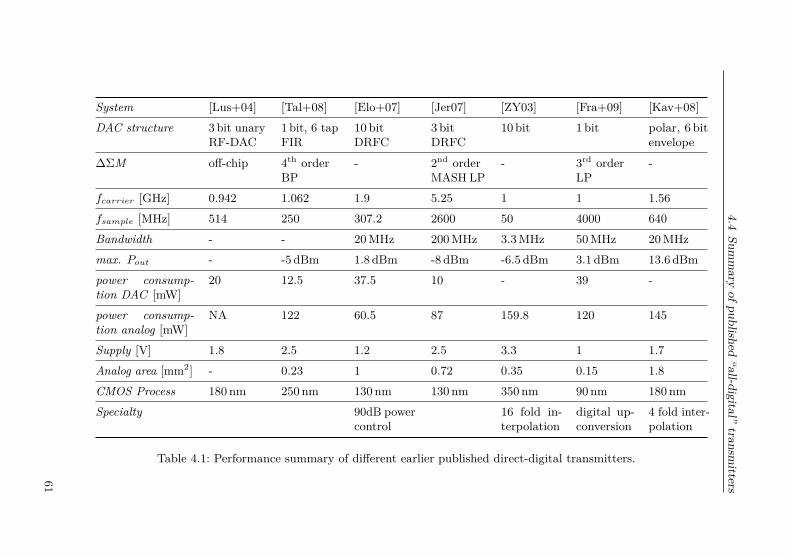
4.4Sum
mary
ofpublished“all-digital”
transmitters
System [Lus+04] [Tal+08] [Elo+07] [Jer07] [ZY03] [Fra+09] [Kav+08]DAC structure 3 bit unary
RF-DAC1bit, 6 tapFIR
10 bitDRFC
3bitDRFC
10 bit 1 bit polar, 6 bitenvelope
∆ΣM off-chip 4th orderBP
- 2nd orderMASH LP
- 3rd orderLP
-
fcarrier [GHz] 0.942 1.062 1.9 5.25 1 1 1.56fsample [MHz] 514 250 307.2 2600 50 4000 640Bandwidth - - 20MHz 200MHz 3.3MHz 50MHz 20MHzmax. Pout - -5 dBm 1.8 dBm -8 dBm -6.5 dBm 3.1 dBm 13.6 dBmpower consump-tion DAC [mW]
20 12.5 37.5 10 - 39 -
power consump-tion analog [mW]
NA 122 60.5 87 159.8 120 145
Supply [V] 1.8 2.5 1.2 2.5 3.3 1 1.7
Analog area [mm2] - 0.23 1 0.72 0.35 0.15 1.8CMOS Process 180 nm 250 nm 130 nm 130 nm 350 nm 90 nm 180 nmSpecialty 90dB power
control16 fold in-terpolation
digital up-conversion
4 fold inter-polation
Table 4.1: Performance summary of different earlier published direct-digital transmitters.
61

62
5 RF-DAC Transmitter System Requirements
Before the circuit implementation of the RF-DAC transmitter can be started,the system requirements, depending on the targeted communications system,have to be defined. A suitable transmitter architecture has to be found andspecific requirements for the main building-blocks have to be derived from theoverall system specifications.
System simulations allow to estimate the influence of different parameter andarchitectural choices on the overall system performance. All system simulationsfor this thesis have been conducted utilizing Matlab®.
5.1 Supported standards and performance requirements
The RF-DAC based transmitter should be compatible with high-data-rate,broadband communication standards such as WLAN IEEE 802.11 or 3GPPLTE. At the same time also other communication standards such as GSM,WCDMA or Bluetooth (BT) with lower data rates and bandwidths should besupported. Most modern high-data-rate communication standards are based onOFDM signal processing, as explained in chapter 2.4. Therefore, the transmitterfrontend should be suited for the OFDM signal requirements, e.g. have anadequate linearity and sufficient dynamic range to support high peak-to-averagepower ratios. The supported signal bandwidth should be at least 20MHz, whichis the typical maximum bandwidth of LTE and WLAN signals. The mostimportant signal characteristics of the LTE and WLAN IEEE 802.11n standardsare summarized in table 2.1.
5.1.1 Supported frequency bands
Although a lot of different frequency bands are specified for the cellular standards,all existing GSM and WCDMA nets operate at frequencies below 2GHz. Thefrequency bands for connectivity devices (WLAN and BT) are the ISM (industrial,scientific, medical) bands around 2.4GHz and 5.8GHz. The ISM band at 2.4GHzis, however, much more popular than the 5.8GHz band, because of the betterpropagation characteristics of the electromagnetic waves. Additionally, therequired implementation effort and thus cost for the devices is reduced for lowerfrequencies.
63
5 RF-DAC Transmitter System Requirements
For the 3GPP LTE communication standard, a lot of different frequency bandsare specified. However, not all frequency bands are equally attractive, as they forexample differ in available bandwidth, wave propagation characteristics, FDDduplex gap distance etc. Furthermore, not all of the bands are unoccupied inevery country.The first frequency bands that will be used (at least in Germany) are a
frequency band around 800MHz – which was previously used for analog televisionbroadcast – as well as formerly unused frequency bands at around 2.6GHz. LTEband VII is a frequency band with frequency division duplex (FDD) operationwith uplink (from the mobile device to the base station) frequencies from 2500 to2570MHz and downlink (from the basestation to the mobile device) frequenciesfrom 2620 to 2690MHz. Interestingly, another frequency band (band 38) isplanned with time division duplex (TDD) operation within the 50MHz wideduplex gap of band VII.In summary, it can be said that a transmitter that allows the operation at
frequencies up to 2620MHz may cover all relevant frequency bands for cellularand connectivity wireless communication standards.
5.1.2 Output power considerations
The maximum peak output power of mobile telecommunication devices forGSM, UMTS, and LTE is in the range of +33 dBm. These high output powerlevels can neither be achieved with a CMOS RF modulator directly nor withan RF modulator plus on-chip CMOS PA, as discussed in chapter 3. Therefore,an external PA is needed. Still, the output power of the RF-DAC should beas high as possible. An output power level in the range of +15 dBm wouldpermit relatively simple, external PAs. A low required PA power gain allows theimplementation of the PA with a low number of amplifier stages, lowering theoff-chip component costs and improving the power added efficiency (PAE) ofthe PA. When the transmitter is operated in backoff at power levels much belowthe peak output power – where e.g. WCDMA devices are operated for most ofthe time – the PA could even be bypassed and switched off, to maximize powerefficiency. For some connectivity devices with lower required maximum outputpower such as BT and WLAN an external PA could be waived completely.On the other hand, for the circuit implementation of the transmitter it is
important to note that a trade-off between output power and linearity of theRF-DAC exists. A high output power requires large currents in the RF-DAC andhence transistors with a large aspect ratio. This, however, reduces the outputimpedance of the RF-DAC and hence linearity.
64
5.2 Determination of the spectral mask
RF-DACD
A
RF-DACD
A
Radio 2 (e.g. GSM, UMTS, LTE, ...)
PA
PA
LNA1LNA2
LNA1LNA2
Radio 1 (e.g. WLAN, BT, ...)
Figure 5.1: Scenario of two parallel running radios on the same mobile device.The transmit signal of radio 2 may disturb its own receiver, if it isrunning in FDD mode. Also, the receiver of the concurrently runningradio 1 may be disturbed.
5.2 Determination of the upper limit for the unwantedemissions and calculation of the spectral mask
Most communication standards define maximum spurious emissions. Still, theseemission limits may not be strict enough if there are several transceivers withinthe same mobile device, in close proximity, and running at the same time. Neigh-boring receivers shall not be disturbed by the transmitter’s spurious emissions.For example, a smartphone user could want to place a phone call via a cellularstandard like GSM, while he is downloading data via WLAN. The strong GSMsignal must not disturb the WLAN receiver. Such a scenario with two concur-rently running radios is depicted in Fig. 5.1. The running transmitter of radio2 could either disturb the receiver of radio 1. Also, the transmitter of radio 2could disturb its own receiver, if these are not properly isolated from each other.
Two effects can lead to a disturbance of a receiver. First, the strong transmitsignal could act as an out-of-band blocker for the receiver, which is runningat another frequency, driving the low noise amplifier (LNA) into compression.Band-select filters at the receiver input, however, should normally be capable ofsuppressing these blocking signals sufficiently. Still, chip and PCB layout have to
65
5 RF-DAC Transmitter System Requirements
be done with great care to circumvent a parasitic coupling from the transmitteroutput directly to the LNA input, bypassing the band-select filters.
The second effect is that the transmitter could emit additional noise at otherfrequencies than its wanted frequency. Unwanted emissions within the receiveband frequencies act as noise for the receiver, which adds up to the normallydominant thermal noise floor. Thereby, the signal-to-noise ratio at the receiverinput is degraded.Unwanted emissions are especially critical for full-duplex FDD system such
as WCDMA or LTE, where the receiver is running at the same time but atanother frequency as the transmitter of the same radio. The frequency spacing –the so-called duplex gap – of transmit and receive bands is typically some tensof MHz. As receiver and transmitter mostly share a common antenna, a SAWduplex filter with very high selectivity is needed to suppress unwanted emissionsof the transmitter at receive frequencies.For half-duplex TDD systems such as GSM and WLAN, receiver and trans-
mitter run at the same frequency but at different time slots. Thereby, thetransmitter can not disturb its own receiver. Anyhow, the transmitter of such asystem could still disturb a simultaneously running receiver of another radio onthe same device.The communication standard’s transmit specifications give valid adjacent
channel and general far-off spurious emission limits. But for the receive bands ofradios on the same mobile device a stricter spectral mask than the one definedby the communication standard must be used.To estimate how big the maximum additional emitted noise in the receive
bands may be, it is assumed that the receiver input sensitivity should not bedegraded by more than 1 dB, to sustain a low bit error rate. The thermal noisePN , normalized to a bandwidth of 1Hz, at room temperature (T0 = 290 K) is
PN = kB · T0 = 1.38 · 10−23 J/K · 290K= 4 · 10−18mW/Hz = −174dBm/Hz, (5.1)
where kB is the Boltzmann constant.Thus, the overall noise at the receiver input may not exceed PN + 1 dB =−173 dBm/Hz. To achieve this, the additional spurious emissions at the receiverinput Pspurrx must be limited to
Pspurrx = 10 · log10
(10
−17310 − 10
−17410
) dBmHz = −179.8 dBm
Hz .
Thus, if we restrict the receiver sensitivity degradation to 1 dB the additionalnoise must be at least a factor of four lower than the thermal noise floor!
On their way to the receiver input, transmitted spurious emissions are dampedby the transmitter’s (duplex) SAW filter (LSAW ), the receiver’s band-select
66
5.3 Matlab system simulations
input filter (Lins) insertion loss, and – as far as transmitter and receiver donot have a shared antenna – the limited coupling between the transmit andreceive antenna (Lant). Therefore, the maximal allowed unwanted emissions atthe transmitter output PspurT x can be written as
PspurT x (f) = PspurRx (f) + LSAW (f) + Lins(f) + Lant(f). (5.2)Especially the damping of SAW filters is very frequency dependent. UMTS andLTE duplex filters are optimized for the duplex frequency spacing, typicallyachieving around 45 to 50 dB isolation in this frequency region. At other frequen-cies more than 25 dB Tx to antenna attenuation are typically obtained [EPC07].The insertion loss Lins of a SAW filter is typically below 2dB. Measurementson mobile phone patch antennas conducted in the lab revealed that a minimumisolation Lant of 20 dB between two antennas in close proximity can be expected[Arl09]. If placed more optimal within the phone, an isolation of 30 to 40 dB isrealistic [Kis09].The maximally allowed unwanted emissions were calculated for frequency
bands where radios are operated simultaneously and independently, such asWLAN, Bluetooth, GPS, and GSM. Especially critical are the receive bands ofFDD systems like UMTS or LTE. The maximum allowed spurious emissionsat the transmitter output are between -130 and -120 dBm/Hz depending onthe frequency band. In Fig. 5.16(a) the resulting spectral mask for an LTEtransmitter operating in the 2.5GHz band is shown.
5.3 Matlab system simulations
The transmitter system, consisting of digital signal generation and modulation,digital signal processing, “direct digital modulator”, as well as the mixed-signaland RF components, has been modeled with Matlab® to enable system simula-tions on a high abstraction level. For the RF blocks, equivalent baseband modelshave been used to increase the simulation speed. Nonlinearities of the transmitterhave been characterized by a simple Saleh model [Jer+00, p. 218 ff.]. This kind ofmodel characterizes consequences of nonlinearities on both amplitude (AM/AMconversion) and phase (AM/PM conversion). Also, some signal post-processinghas been implemented to evaluate the quality of the simulated RF-DAC outputsignal, e.g. to plot the output spectrum and spectral masks or calculate the errorvector magnitude (EVM).
Several simulations to determine spectrum allocation and figures-of-merit likeEVM have been carried out for different standards such as WLAN and LTE, fordifferent bandwidth settings, carrier frequencies, and modulation schemes.The calculations of the above discussed unwanted emission limits have been
conducted with Microsoft Excel® and imported into Matlab to plot the resultingspectral masks for the respective communication standard and frequency band.
67
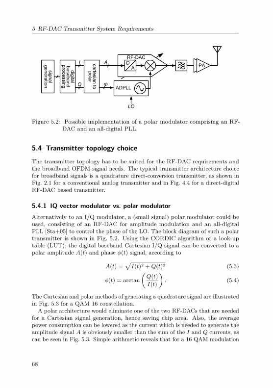
5 RF-DAC Transmitter System Requirements
ADPLL
dig
ital
ba
se
ba
nd
p
roce
ssin
g
I
Q
A
Φ
ca
rtesia
n to
p
ola
r
DA
RF-DAC
LO
PA
sig
na
l g
en
era
tion
Figure 5.2: Possible implementation of a polar modulator comprising an RF-DAC and an all-digital PLL.
5.4 Transmitter topology choice
The transmitter topology has to be suited for the RF-DAC requirements andthe broadband OFDM signal needs. The typical transmitter architecture choicefor broadband signals is a quadrature direct-conversion transmitter, as shown inFig. 2.1 for a conventional analog transmitter and in Fig. 4.4 for a direct-digitalRF-DAC based transmitter.
5.4.1 IQ vector modulator vs. polar modulatorAlternatively to an I/Q modulator, a (small signal) polar modulator could beused, consisting of an RF-DAC for amplitude modulation and an all-digitalPLL [Sta+05] to control the phase of the LO. The block diagram of such a polartransmitter is shown in Fig. 5.2. Using the CORDIC algorithm or a look-uptable (LUT), the digital baseband Cartesian I/Q signal can be converted to apolar amplitude A(t) and phase φ(t) signal, according to
A(t) =√I(t)2 +Q(t)2 (5.3)
φ(t) = arctan(Q(t)I(t)
). (5.4)
The Cartesian and polar methods of generating a quadrature signal are illustratedin Fig. 5.3 for a QAM 16 constellation.
A polar architecture would eliminate one of the two RF-DACs that are neededfor a Cartesian signal generation, hence saving chip area. Also, the averagepower consumption can be lowered as the current which is needed to generate theamplitude signal A is obviously smaller than the sum of the I and Q currents, ascan be seen in Fig. 5.3. Simple arithmetic reveals that for a 16 QAM modulation
68
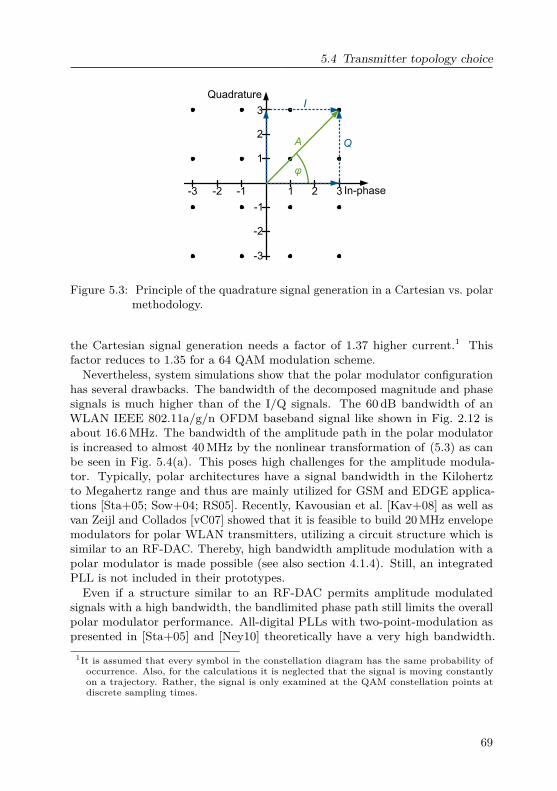
5.4 Transmitter topology choice
In-phase1 2 3-1-2-3
1
2
3
Quadrature
-1
-2
-3
QA
φ
I
Figure 5.3: Principle of the quadrature signal generation in a Cartesian vs. polarmethodology.
the Cartesian signal generation needs a factor of 1.37 higher current.1 Thisfactor reduces to 1.35 for a 64 QAM modulation scheme.
Nevertheless, system simulations show that the polar modulator configurationhas several drawbacks. The bandwidth of the decomposed magnitude and phasesignals is much higher than of the I/Q signals. The 60 dB bandwidth of anWLAN IEEE 802.11a/g/n OFDM baseband signal like shown in Fig. 2.12 isabout 16.6MHz. The bandwidth of the amplitude path in the polar modulatoris increased to almost 40MHz by the nonlinear transformation of (5.3) as canbe seen in Fig. 5.4(a). This poses high challenges for the amplitude modula-tor. Typically, polar architectures have a signal bandwidth in the Kilohertzto Megahertz range and thus are mainly utilized for GSM and EDGE applica-tions [Sta+05; Sow+04; RS05]. Recently, Kavousian et al. [Kav+08] as well asvan Zeijl and Collados [vC07] showed that it is feasible to build 20MHz envelopemodulators for polar WLAN transmitters, utilizing a circuit structure which issimilar to an RF-DAC. Thereby, high bandwidth amplitude modulation with apolar modulator is made possible (see also section 4.1.4). Still, an integratedPLL is not included in their prototypes.Even if a structure similar to an RF-DAC permits amplitude modulated
signals with a high bandwidth, the bandlimited phase path still limits the overallpolar modulator performance. All-digital PLLs with two-point-modulation aspresented in [Sta+05] and [Ney10] theoretically have a very high bandwidth.
1It is assumed that every symbol in the constellation diagram has the same probability ofoccurrence. Also, for the calculations it is neglected that the signal is moving constantlyon a trajectory. Rather, the signal is only examined at the QAM constellation points atdiscrete sampling times.
69
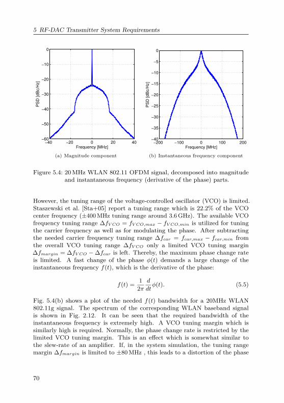
5 RF-DAC Transmitter System Requirements
−40 −20 0 20 40−60
−50
−40
−30
−20
−10
0
Frequency [MHz]
PS
D [dB
c/H
z]
(a) Magnitude component
−200 −100 0 100 200−40
−35
−30
−25
−20
−15
−10
−5
0
Frequency [MHz]P
SD
[dB
c/H
z]
(b) Instantaneous frequency component
Figure 5.4: 20MHz WLAN 802.11 OFDM signal, decomposed into magnitudeand instantaneous frequency (derivative of the phase) parts.
However, the tuning range of the voltage-controlled oscillator (VCO) is limited.Staszewski et al. [Sta+05] report a tuning range which is 22.2% of the VCOcenter frequency (±400MHz tuning range around 3.6GHz). The available VCOfrequency tuning range ∆fV CO = fV CO,max − fV CO,min is utilized for tuningthe carrier frequency as well as for modulating the phase. After subtractingthe needed carrier frequency tuning range ∆fcar = fcar,max − fcar,min fromthe overall VCO tuning range ∆fV CO only a limited VCO tuning margin∆fmargin = ∆fV CO −∆fcar is left. Thereby, the maximum phase change rateis limited. A fast change of the phase φ(t) demands a large change of theinstantaneous frequency f(t), which is the derivative of the phase:
f(t) = 12π
d
dtφ(t). (5.5)
Fig. 5.4(b) shows a plot of the needed f(t) bandwidth for a 20MHz WLAN802.11g signal. The spectrum of the corresponding WLAN baseband signalis shown in Fig. 2.12. It can be seen that the required bandwidth of theinstantaneous frequency is extremely high. A VCO tuning margin which issimilarly high is required. Normally, the phase change rate is restricted by thelimited VCO tuning margin. This is an effect which is somewhat similar tothe slew-rate of an amplifier. If, in the system simulation, the tuning rangemargin ∆fmargin is limited to ±80MHz , this leads to a distortion of the phase
70
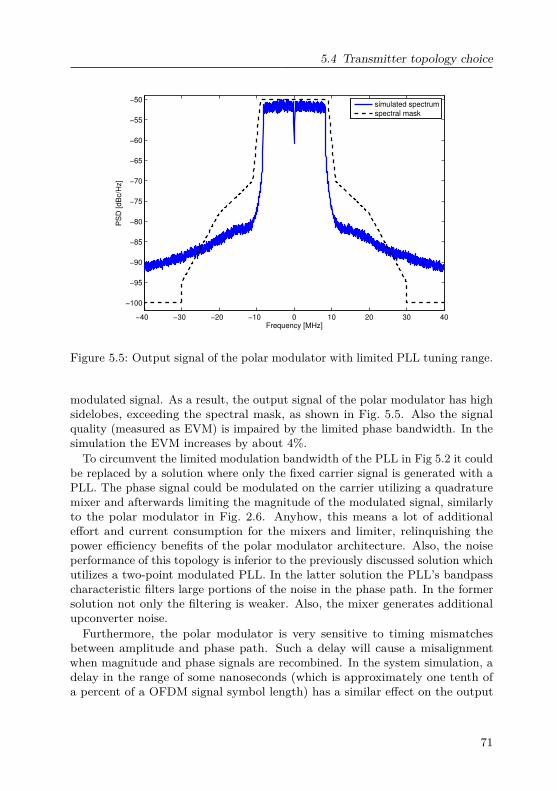
5.4 Transmitter topology choice
−40 −30 −20 −10 0 10 20 30 40
−100
−95
−90
−85
−80
−75
−70
−65
−60
−55
−50
Frequency [MHz]
PS
D [dB
c/H
z]
simulated spectrum
spectral mask
Figure 5.5: Output signal of the polar modulator with limited PLL tuning range.
modulated signal. As a result, the output signal of the polar modulator has highsidelobes, exceeding the spectral mask, as shown in Fig. 5.5. Also the signalquality (measured as EVM) is impaired by the limited phase bandwidth. In thesimulation the EVM increases by about 4%.
To circumvent the limited modulation bandwidth of the PLL in Fig 5.2 it couldbe replaced by a solution where only the fixed carrier signal is generated with aPLL. The phase signal could be modulated on the carrier utilizing a quadraturemixer and afterwards limiting the magnitude of the modulated signal, similarlyto the polar modulator in Fig. 2.6. Anyhow, this means a lot of additionaleffort and current consumption for the mixers and limiter, relinquishing thepower efficiency benefits of the polar modulator architecture. Also, the noiseperformance of this topology is inferior to the previously discussed solution whichutilizes a two-point modulated PLL. In the latter solution the PLL’s bandpasscharacteristic filters large portions of the noise in the phase path. In the formersolution not only the filtering is weaker. Also, the mixer generates additionalupconverter noise.Furthermore, the polar modulator is very sensitive to timing mismatches
between amplitude and phase path. Such a delay will cause a misalignmentwhen magnitude and phase signals are recombined. In the system simulation, adelay in the range of some nanoseconds (which is approximately one tenth ofa percent of a OFDM signal symbol length) has a similar effect on the output
71
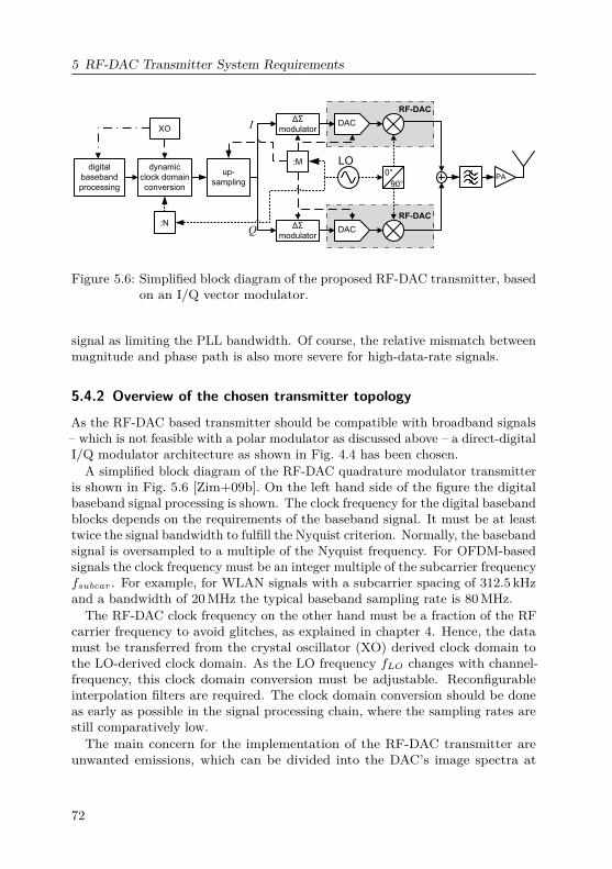
5 RF-DAC Transmitter System Requirements
digital
baseband
processing
dynamic
clock domain
conversion
ΔΣ
modulator
PA
DACXO
:M
ΔΣ
modulatorDAC
I
Q
0°
90°
RF-DAC
RF-DAC:N
up-
sampling
LO
Figure 5.6: Simplified block diagram of the proposed RF-DAC transmitter, basedon an I/Q vector modulator.
signal as limiting the PLL bandwidth. Of course, the relative mismatch betweenmagnitude and phase path is also more severe for high-data-rate signals.
5.4.2 Overview of the chosen transmitter topology
As the RF-DAC based transmitter should be compatible with broadband signals– which is not feasible with a polar modulator as discussed above – a direct-digitalI/Q modulator architecture as shown in Fig. 4.4 has been chosen.
A simplified block diagram of the RF-DAC quadrature modulator transmitteris shown in Fig. 5.6 [Zim+09b]. On the left hand side of the figure the digitalbaseband signal processing is shown. The clock frequency for the digital basebandblocks depends on the requirements of the baseband signal. It must be at leasttwice the signal bandwidth to fulfill the Nyquist criterion. Normally, the basebandsignal is oversampled to a multiple of the Nyquist frequency. For OFDM-basedsignals the clock frequency must be an integer multiple of the subcarrier frequencyfsubcar. For example, for WLAN signals with a subcarrier spacing of 312.5 kHzand a bandwidth of 20MHz the typical baseband sampling rate is 80MHz.
The RF-DAC clock frequency on the other hand must be a fraction of the RFcarrier frequency to avoid glitches, as explained in chapter 4. Hence, the datamust be transferred from the crystal oscillator (XO) derived clock domain tothe LO-derived clock domain. As the LO frequency fLO changes with channel-frequency, this clock domain conversion must be adjustable. Reconfigurableinterpolation filters are required. The clock domain conversion should be doneas early as possible in the signal processing chain, where the sampling rates arestill comparatively low.The main concern for the implementation of the RF-DAC transmitter are
unwanted emissions, which can be divided into the DAC’s image spectra at
72
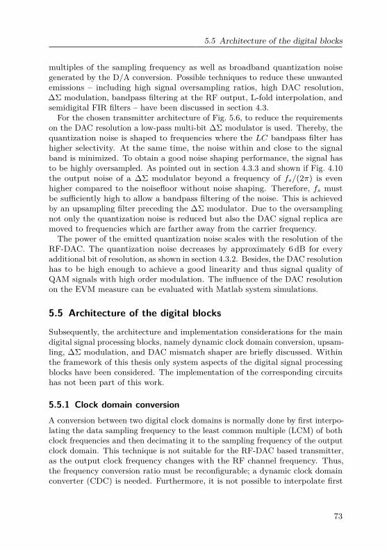
5.5 Architecture of the digital blocks
multiples of the sampling frequency as well as broadband quantization noisegenerated by the D/A conversion. Possible techniques to reduce these unwantedemissions – including high signal oversampling ratios, high DAC resolution,∆Σ modulation, bandpass filtering at the RF output, L-fold interpolation, andsemidigital FIR filters – have been discussed in section 4.3.
For the chosen transmitter architecture of Fig. 5.6, to reduce the requirementson the DAC resolution a low-pass multi-bit ∆Σ modulator is used. Thereby, thequantization noise is shaped to frequencies where the LC bandpass filter hashigher selectivity. At the same time, the noise within and close to the signalband is minimized. To obtain a good noise shaping performance, the signal hasto be highly oversampled. As pointed out in section 4.3.3 and shown if Fig. 4.10the output noise of a ∆Σ modulator beyond a frequency of fs/(2π) is evenhigher compared to the noisefloor without noise shaping. Therefore, fs mustbe sufficiently high to allow a bandpass filtering of the noise. This is achievedby an upsampling filter preceding the ∆Σ modulator. Due to the oversamplingnot only the quantization noise is reduced but also the DAC signal replica aremoved to frequencies which are farther away from the carrier frequency.
The power of the emitted quantization noise scales with the resolution of theRF-DAC. The quantization noise decreases by approximately 6 dB for everyadditional bit of resolution, as shown in section 4.3.2. Besides, the DAC resolutionhas to be high enough to achieve a good linearity and thus signal quality ofQAM signals with high order modulation. The influence of the DAC resolutionon the EVM measure can be evaluated with Matlab system simulations.
5.5 Architecture of the digital blocks
Subsequently, the architecture and implementation considerations for the maindigital signal processing blocks, namely dynamic clock domain conversion, upsam-ling, ∆Σ modulation, and DAC mismatch shaper are briefly discussed. Withinthe framework of this thesis only system aspects of the digital signal processingblocks have been considered. The implementation of the corresponding circuitshas not been part of this work.
5.5.1 Clock domain conversionA conversion between two digital clock domains is normally done by first interpo-lating the data sampling frequency to the least common multiple (LCM) of bothclock frequencies and then decimating it to the sampling frequency of the outputclock domain. This technique is not suitable for the RF-DAC based transmitter,as the output clock frequency changes with the RF channel frequency. Thus,the frequency conversion ratio must be reconfigurable; a dynamic clock domainconverter (CDC) is needed. Furthermore, it is not possible to interpolate first
73
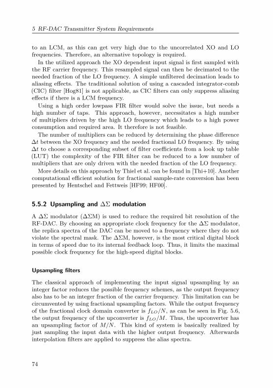
5 RF-DAC Transmitter System Requirements
to an LCM, as this can get very high due to the uncorrelated XO and LOfrequencies. Therefore, an alternative topology is required.
In the utilized approach the XO dependent input signal is first sampled withthe RF carrier frequency. This resampled signal can then be decimated to theneeded fraction of the LO frequency. A simple unfiltered decimation leads toaliasing effects. The traditional solution of using a cascaded integrator-comb(CIC) filter [Hog81] is not applicable, as CIC filters can only suppress aliasingeffects if there is a LCM frequency.Using a high order lowpass FIR filter would solve the issue, but needs a
high number of taps. This approach, however, necessitates a high numberof multipliers driven by the high LO frequency which leads to a high powerconsumption and required area. It therefore is not feasible.
The number of multipliers can be reduced by determining the phase difference∆t between the XO frequency and the needed fractional LO frequency. By using∆t to choose a corresponding subset of filter coefficients from a look up table(LUT) the complexity of the FIR filter can be reduced to a low number ofmultipliers that are only driven with the needed fraction of the LO frequency.
More details on this approach by Thiel et al. can be found in [Thi+10]. Anothercomputational efficient solution for fractional sample-rate conversion has beenpresented by Hentschel and Fettweis [HF99; HF00].
5.5.2 Upsampling and ∆Σ modulation
A ∆Σ modulator (∆ΣM) is used to reduce the required bit resolution of theRF-DAC. By choosing an appropriate clock frequency for the ∆Σ modulator,the replica spectra of the DAC can be moved to a frequency where they do notviolate the spectral mask. The ∆ΣM, however, is the most critical digital blockin terms of speed due to its internal feedback loop. Thus, it limits the maximalpossible clock frequency for the high-speed digital blocks.
Upsampling filters
The classical approach of implementing the input signal upsampling by aninteger factor reduces the possible frequency schemes, as the output frequencyalso has to be an integer fraction of the carrier frequency. This limitation can becircumvented by using fractional upsampling factors. While the output frequencyof the fractional clock domain converter is fLO/N , as can be seen in Fig. 5.6,the output frequency of the upconverter is fLO/M . Thus, the upconverter hasan upsampling factor of M/N . This kind of system is basically realized byjust sampling the input data with the higher output frequency. Afterwardsinterpolation filters are applied to suppress the alias spectra.
74
5.5 Architecture of the digital blocks
D Qin D Q
Programmable delay
lineD Q...
D Q
out
fout
Figure 5.7: Implementation of one interpolation filter stage.
time
time
freq.
freq.
1
-T/2 T/2
-aT/2 aT/2
T
-3T
-2T
-1T
1T
2T
3T
-5
aT
-2
aT
-1
aT
-3
aT
1 aT
-4
aT
-6
aT
1
aT
2aT
3aT
4aT
5aT
Figure 5.8: Filter response of one interpolation filter stage in the time andfrequency domain for different filter length.
The interpolation filters are realized as rectangular brick-wall filters in thetime domain, which have a sinc response in the frequency domain. A blockdiagram of the filter structure is shown in Fig. 5.7. The filter bandwidth can beset by programming the length of the delay line. The bandwidth of the filter isinversely proportional to the filter length T in the time domain:
rect(t
T
) c sT sin(πTf)πTf
= T · sinc(Tf). (5.6)
The frequency response for different filter lengths is depicted in Fig. 5.8. Thistype of filter has the advantage that it is simple to realize and can still beimplemented for high clock frequencies. To obtain a good alias suppression, upto three filters with different filter lengths and thus corner frequencies can beapplied in series. As can be seen from equation (5.6) the filter has an amplitudegain which depends on the filter length T . The output amplitude of the filtertherefore has to be adjusted by a gain normalization step, to circumvent overflowsin the subsequent digital circuits.
75
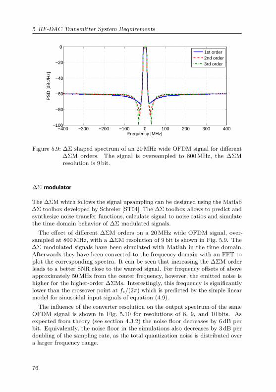
5 RF-DAC Transmitter System Requirements
−400 −300 −200 −100 0 100 200 300 400−100
−80
−60
−40
−20
0
Frequency [MHz]
PS
D [d
Bc/
Hz]
1st order2nd order3rd order
Figure 5.9: ∆Σ shaped spectrum of an 20MHz wide OFDM signal for different∆ΣM orders. The signal is oversampled to 800MHz, the ∆ΣMresolution is 9 bit.
∆Σ modulator
The ∆ΣM which follows the signal upsampling can be designed using the Matlab∆Σ toolbox developed by Schreier [ST04]. The ∆Σ toolbox allows to predict andsynthesize noise transfer functions, calculate signal to noise ratios and simulatethe time domain behavior of ∆Σ modulated signals.The effect of different ∆ΣM orders on a 20MHz wide OFDM signal, over-
sampled at 800MHz, with a ∆ΣM resolution of 9 bit is shown in Fig. 5.9. The∆Σ modulated signals have been simulated with Matlab in the time domain.Afterwards they have been converted to the frequency domain with an FFT toplot the corresponding spectra. It can be seen that increasing the ∆ΣM orderleads to a better SNR close to the wanted signal. For frequency offsets of aboveapproximately 50MHz from the center frequency, however, the emitted noise ishigher for the higher-order ∆ΣMs. Interestingly, this frequency is significantlylower than the crossover point at fs/(2π) which is predicted by the simple linearmodel for sinusoidal input signals of equation (4.9).
The influence of the converter resolution on the output spectrum of the sameOFDM signal is shown in Fig. 5.10 for resolutions of 8, 9, and 10 bits. Asexpected from theory (see section 4.3.2) the noise floor decreases by 6 dB perbit. Equivalently, the noise floor in the simulations also decreases by 3 dB perdoubling of the sampling rate, as the total quantization noise is distributed overa larger frequency range.
76
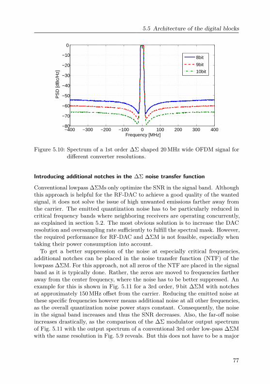
5.5 Architecture of the digital blocks
−400 −300 −200 −100 0 100 200 300 400−80
−70
−60
−50
−40
−30
−20
−10
0
Frequency [MHz]
PS
D [d
Bc/
Hz]
8bit
9bit
10bit
Figure 5.10: Spectrum of a 1st order ∆Σ shaped 20MHz wide OFDM signal fordifferent converter resolutions.
Introducing additional notches in the ∆Σ noise transfer function
Conventional lowpass ∆ΣMs only optimize the SNR in the signal band. Althoughthis approach is helpful for the RF-DAC to achieve a good quality of the wantedsignal, it does not solve the issue of high unwanted emissions farther away fromthe carrier. The emitted quantization noise has to be particularly reduced incritical frequency bands where neighboring receivers are operating concurrently,as explained in section 5.2. The most obvious solution is to increase the DACresolution and oversampling rate sufficiently to fulfill the spectral mask. However,the required performance for RF-DAC and ∆ΣM is not feasible, especially whentaking their power consumption into account.To get a better suppression of the noise at especially critical frequencies,
additional notches can be placed in the noise transfer function (NTF) of thelowpass ∆ΣM. For this approach, not all zeros of the NTF are placed in the signalband as it is typically done. Rather, the zeros are moved to frequencies fartheraway from the center frequency, where the noise has to be better suppressed. Anexample for this is shown in Fig. 5.11 for a 3rd order, 9 bit ∆ΣM with notchesat approximately 150MHz offset from the carrier. Reducing the emitted noise atthese specific frequencies however means additional noise at all other frequencies,as the overall quantization noise power stays constant. Consequently, the noisein the signal band increases and thus the SNR decreases. Also, the far-off noiseincreases drastically, as the comparison of the ∆Σ modulator output spectrumof Fig. 5.11 with the output spectrum of a conventional 3rd order low-pass ∆ΣMwith the same resolution in Fig. 5.9 reveals. But this does not have to be a major
77
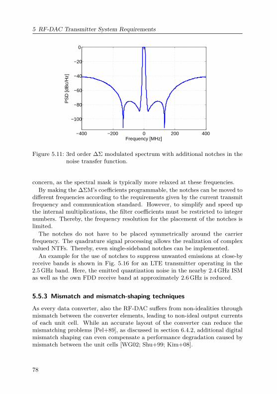
5 RF-DAC Transmitter System Requirements
−400 −200 0 200 400
−100
−80
−60
−40
−20
0
Frequency [MHz]
PS
D [d
Bc/
Hz]
Figure 5.11: 3rd order ∆Σ modulated spectrum with additional notches in thenoise transfer function.
concern, as the spectral mask is typically more relaxed at these frequencies.By making the ∆ΣM’s coefficients programmable, the notches can be moved to
different frequencies according to the requirements given by the current transmitfrequency and communication standard. However, to simplify and speed upthe internal multiplications, the filter coefficients must be restricted to integernumbers. Thereby, the frequency resolution for the placement of the notches islimited.The notches do not have to be placed symmetrically around the carrier
frequency. The quadrature signal processing allows the realization of complexvalued NTFs. Thereby, even single-sideband notches can be implemented.
An example for the use of notches to suppress unwanted emissions at close-byreceive bands is shown in Fig. 5.16 for an LTE transmitter operating in the2.5GHz band. Here, the emitted quantization noise in the nearby 2.4GHz ISMas well as the own FDD receive band at approximately 2.6GHz is reduced.
5.5.3 Mismatch and mismatch-shaping techniques
As every data converter, also the RF-DAC suffers from non-idealities throughmismatch between the converter elements, leading to non-ideal output currentsof each unit cell. While an accurate layout of the converter can reduce themismatching problems [Pel+89], as discussed in section 6.4.2, additional digitalmismatch shaping can even compensate a performance degradation caused bymismatch between the unit cells [WG02; Shu+99; Kim+08].
78
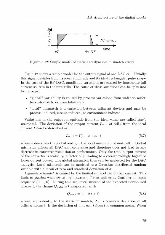
5.5 Architecture of the digital blocks
timemagnitude
kT (k+1)T
I(1+ε+es,i)
Figure 5.12: Simple model of static and dynamic mismatch errors.
Fig. 5.12 shows a simple model for the output signal of one DAC cell. Usually,this signal deviates from its ideal amplitude and its ideal rectangular pulse shape.In the case of the RF-DAC, amplitude variations are caused by inaccurate tailcurrent sources in the unit cells. The cause of these variations can be split intotwo groups:
• “global” variability is caused by process variations from wafer-to-wafer,batch-to-batch, or even fab-to-fab.
• “local” mismatch is a variation between adjacent devices and may beprocess-induced, circuit-induced, or environment-induced.
Variations in the output magnitude from the ideal value are called staticmismatch. The deviation of the output current Iout,i of cell i from the idealcurrent I can be described as
Iout,i = I(1 + ε+ es,i) (5.7)
where ε describes the global and es,i the local mismatch of unit cell i. Globalmismatch affects all DAC unit cells alike and therefore does not lead to anydecrease in converter resolution or performance. Only the total output currentof the converter is scaled by a factor of ε, leading to a correspondingly higher orlower output power. The global mismatch thus can be neglected for the DACanalysis. Local mismatch can be modeled as a Gaussian distributed randomvariable with a mean of zero and standard deviation of σI .
Dynamic mismatch is caused by the limited slope of the output current. Thisleads to glitches when switching between different unit cells. Consider an inputsequence (0, 1, 0). During this sequence, instead of the expected normalizedcharge 1, the charge Qout,i is transported, with
Qout,i = 1 + ∆τ + δi (5.8)
where, equivalently to the static mismatch, ∆τ is common deviation of allcells, whereas δi is the deviation of unit cell i from the common mean. When
79
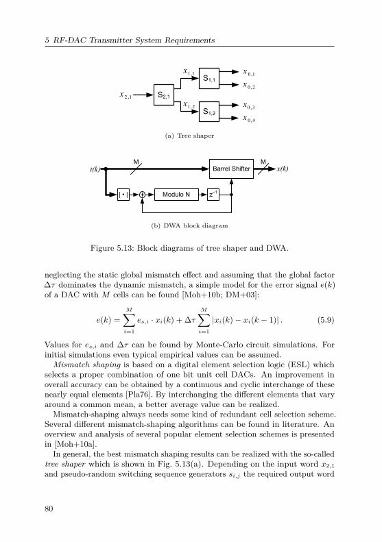
5 RF-DAC Transmitter System Requirements
S2,1
S1,1
S1,2
1,2x
1,1x
2,1x
1,0x
2,0x
3,0x
4,0x
(a) Tree shaper
Modulo N
Barrel Shifter
| • | z−1
M M
t(k) x(k)
(b) DWA block diagram
Figure 5.13: Block diagrams of tree shaper and DWA.
neglecting the static global mismatch effect and assuming that the global factor∆τ dominates the dynamic mismatch, a simple model for the error signal e(k)of a DAC with M cells can be found [Moh+10b; DM+03]:
e(k) =M∑i=1
es,i · xi(k) + ∆τM∑i=1
|xi(k)− xi(k − 1)| . (5.9)
Values for es,i and ∆τ can be found by Monte-Carlo circuit simulations. Forinitial simulations even typical empirical values can be assumed.Mismatch shaping is based on a digital element selection logic (ESL) which
selects a proper combination of one bit unit cell DACs. An improvement inoverall accuracy can be obtained by a continuous and cyclic interchange of thesenearly equal elements [Pla76]. By interchanging the different elements that varyaround a common mean, a better average value can be realized.
Mismatch-shaping always needs some kind of redundant cell selection scheme.Several different mismatch-shaping algorithms can be found in literature. Anoverview and analysis of several popular element selection schemes is presentedin [Moh+10a].
In general, the best mismatch shaping results can be realized with the so-calledtree shaper which is shown in Fig. 5.13(a). Depending on the input word x2,1and pseudo-random switching sequence generators si,j the required output word
80
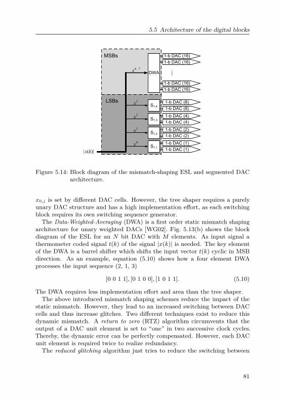
5.5 Architecture of the digital blocks
1-b DAC (16)
1-b DAC (16)
1-b DAC (2)
1-b DAC (2)
1-b DAC (1)
1-b DAC (1)
1-b DAC (16)
1-b DAC (16)
1-b DAC (8)
1-b DAC (8)
1-b DAC (4)
1-b DAC (4)
S1,2
S1,1
DWA
S1,4
S1,3
...
LSBs
MSBs
x4...7
x3
x2
x1
x0
|x(k)|
Figure 5.14: Block diagram of the mismatch-shaping ESL and segmented DACarchitecture.
x0,j is set by different DAC cells. However, the tree shaper requires a purelyunary DAC structure and has a high implementation effort, as each switchingblock requires its own switching sequence generator.
The Data-Weighted-Averaging (DWA) is a first order static mismatch shapingarchitecture for unary weighted DACs [WG02]. Fig. 5.13(b) shows the blockdiagram of the ESL for an N bit DAC with M elements. As input signal athermometer coded signal t(k) of the signal |x(k)| is needed. The key elementof the DWA is a barrel shifter which shifts the input vector t(k) cyclic in MSBdirection. As an example, equation (5.10) shows how a four element DWAprocesses the input sequence (2, 1, 3)
[0 0 1 1], [0 1 0 0], [1 0 1 1]. (5.10)
The DWA requires less implementation effort and area than the tree shaper.The above introduced mismatch shaping schemes reduce the impact of the
static mismatch. However, they lead to an increased switching between DACcells and thus increase glitches. Two different techniques exist to reduce thisdynamic mismatch. A return to zero (RTZ) algorithm circumvents that theoutput of a DAC unit element is set to “one” in two successive clock cycles.Thereby, the dynamic error can be perfectly compensated. However, each DACunit element is required twice to realize redundancy.The reduced glitching algorithm just tries to reduce the switching between
81
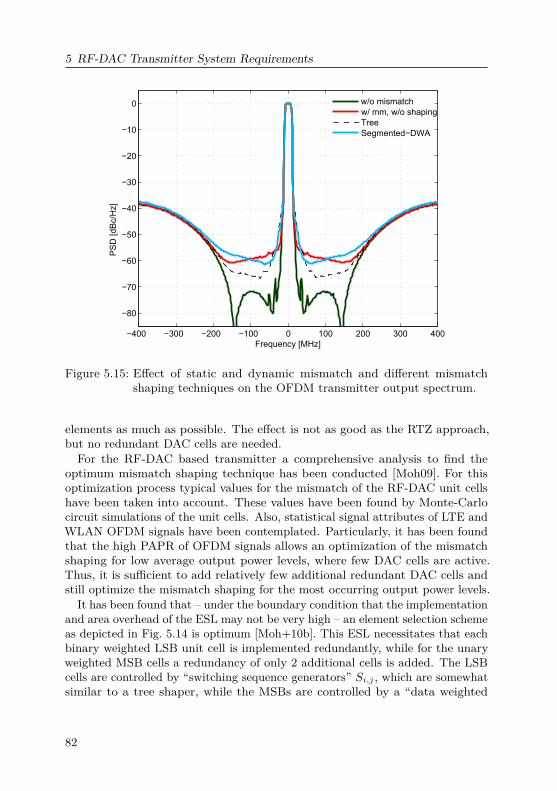
5 RF-DAC Transmitter System Requirements
−400 −300 −200 −100 0 100 200 300 400
−80
−70
−60
−50
−40
−30
−20
−10
0
Frequency [MHz]
PS
D [d
Bc/
Hz]
w/o mismatchw/ mm, w/o shapingTreeSegmented−DWA
Figure 5.15: Effect of static and dynamic mismatch and different mismatchshaping techniques on the OFDM transmitter output spectrum.
elements as much as possible. The effect is not as good as the RTZ approach,but no redundant DAC cells are needed.For the RF-DAC based transmitter a comprehensive analysis to find the
optimum mismatch shaping technique has been conducted [Moh09]. For thisoptimization process typical values for the mismatch of the RF-DAC unit cellshave been taken into account. These values have been found by Monte-Carlocircuit simulations of the unit cells. Also, statistical signal attributes of LTE andWLAN OFDM signals have been contemplated. Particularly, it has been foundthat the high PAPR of OFDM signals allows an optimization of the mismatchshaping for low average output power levels, where few DAC cells are active.Thus, it is sufficient to add relatively few additional redundant DAC cells andstill optimize the mismatch shaping for the most occurring output power levels.
It has been found that – under the boundary condition that the implementationand area overhead of the ESL may not be very high – an element selection schemeas depicted in Fig. 5.14 is optimum [Moh+10b]. This ESL necessitates that eachbinary weighted LSB unit cell is implemented redundantly, while for the unaryweighted MSB cells a redundancy of only 2 additional cells is added. The LSBcells are controlled by “switching sequence generators” Si,j , which are somewhatsimilar to a tree shaper, while the MSBs are controlled by a “data weighted
82
5.6 Final system simulation results
averaging” (DWA) ESL.The effect of mismatch and mismatch shaping is shown in the system simulation
result of Fig. 5.15. A combination of static mismatch with δI = 0.1 and dynamicmismatch of ∆τ = −0.05 would lead to a dramatic increase of the noise floorclose to the wanted signal (red curve). A tree shaper with unary weighted DACscells (black, dashed curve) could significantly improve the matching and thusalso the spectrum. However, it has a prohibitively high implementation effort.The performance of the chosen segmented-DWA architecture (blue curve) allowsto reduce the unwanted emissions up to 6 dB at 45MHz offset from the carrierwhile only having low additional area and power dissipation (2700µm2, 2.8mW).
5.6 Final system simulation results
Several Matlab system simulations have been conducted for different commu-nication standards and settings to determine the required system performanceand specify parameters and performance requirements for the different buildingblocks.
It has been found, that one of the most critical scenarios in terms of unwantedspurious emissions is the operation of the transmitter in LTE band VII in the2.5GHz frequency band. This band is one of the first LTE frequency bands thatwill be used [Eri09]. It is especially critical, as the Tx band is centered betweenthe close-by 2.4GHz ISM band and the own Rx FDD band with a quite smallduplex gap.
Fig. 5.16(a) shows the output spectrum of the transmitter in LTE mode withthe larges specified signal bandwidth of 18MHz. The carrier frequency fcar is2540MHz, which is in LTE band VII, and the Tx output power is set to 23 dBm(LTE class 3 device).
For the LC bandpass filter, a quality factor of 15 has been assumed.To prevent the RF-DAC image frequencies from falling into parallel running
GSM bands (DCS/PCS) the ∆Σ and RF-DAC clock frequency must be set to(at least) fcar/3 (=846.66MHz). A third-order ∆Σ modulator with notchesin the NTF at the critical neighboring receive bands, as it was introduced insection 5.5.2, has been used. The simulations reveal that the resolution of theRF-DAC must be at least 9 bit to meet the spectral mask.Fig. 5.16(b) shows a closeup of the wanted band’s spectrum. As can be
seen, the adjacent channel power ratio (ACPR) is far below the allowed limit,leaving space for strong PA nonlinearities, which have not been included in thesimulations. The small spurs around 20MHz and 35MHz offset are caused bythe imperfect resampling of the dynamic clock domain conversion but are smallenough to not impair the performance of the transmitter.Besides fulfilling spurious emission limits, also the signal quality is of crucial
83
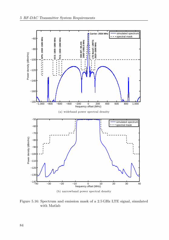
5 RF-DAC Transmitter System Requirements
−1.000 −800 −600 −400 −200 0 200 400 600 800 1.000−180
−160
−140
−120
−100
−80
−60
frequency offset (MHz)
Pow
er d
ensi
ty (
dBm
/Hz)
GP
S: 1
559−
1585
MH
z
DC
S: 1
805−
1880
MH
z
PC
S: 1
930−
1990
MH
z
ISM
(B
T, W
LAN
: 24
00−2
483.
5 M
Hz
LTE
Ban
d7, U
MT
S:
262
0−26
90 M
Hz
Carrier: 2554 MHz simulated spectrumspectral mask
(a) wideband power spectral density
−40 −30 −20 −10 0 10 20 30 40−140
−130
−120
−110
−100
−90
−80
−70
−60
−50
frequency offset (MHz)
Pow
er d
ensi
ty (
dBm
/Hz)
simulated spectrumspectral mask
(b) narrowband power spectral density
Figure 5.16: Spectrum and emission mask of a 2.5GHz LTE signal, simulatedwith Matlab
84
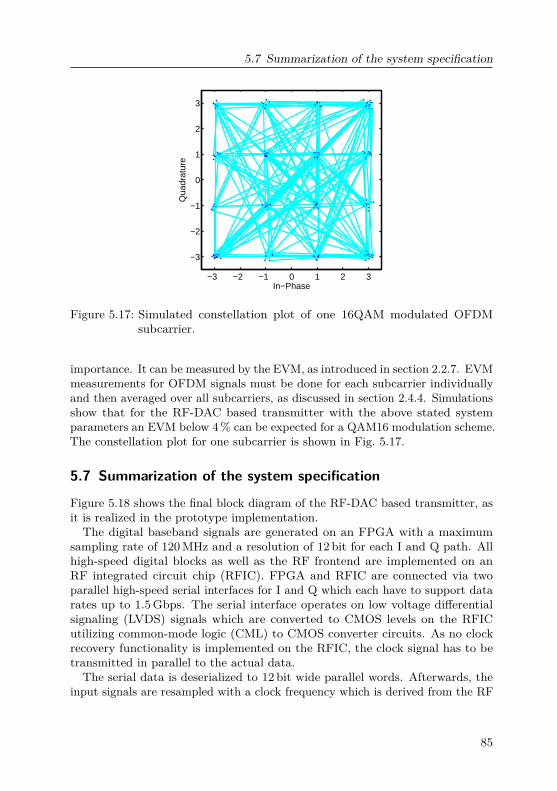
5.7 Summarization of the system specification
−3 −2 −1 0 1 2 3
−3
−2
−1
0
1
2
3
Qua
drat
ure
In−Phase
Figure 5.17: Simulated constellation plot of one 16QAM modulated OFDMsubcarrier.
importance. It can be measured by the EVM, as introduced in section 2.2.7. EVMmeasurements for OFDM signals must be done for each subcarrier individuallyand then averaged over all subcarriers, as discussed in section 2.4.4. Simulationsshow that for the RF-DAC based transmitter with the above stated systemparameters an EVM below 4% can be expected for a QAM16 modulation scheme.The constellation plot for one subcarrier is shown in Fig. 5.17.
5.7 Summarization of the system specification
Figure 5.18 shows the final block diagram of the RF-DAC based transmitter, asit is realized in the prototype implementation.The digital baseband signals are generated on an FPGA with a maximum
sampling rate of 120MHz and a resolution of 12 bit for each I and Q path. Allhigh-speed digital blocks as well as the RF frontend are implemented on anRF integrated circuit chip (RFIC). FPGA and RFIC are connected via twoparallel high-speed serial interfaces for I and Q which each have to support datarates up to 1.5Gbps. The serial interface operates on low voltage differentialsignaling (LVDS) signals which are converted to CMOS levels on the RFICutilizing common-mode logic (CML) to CMOS converter circuits. As no clockrecovery functionality is implemented on the RFIC, the clock signal has to betransmitted in parallel to the actual data.The serial data is deserialized to 12 bit wide parallel words. Afterwards, the
input signals are resampled with a clock frequency which is derived from the RF
85
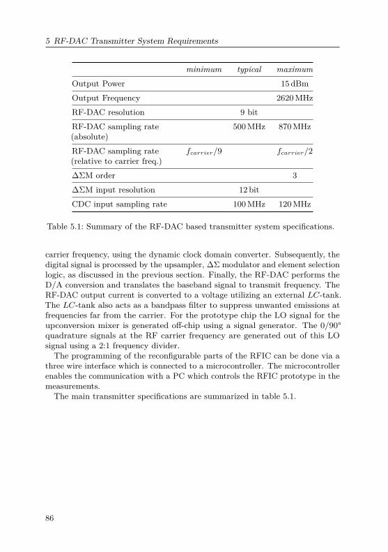
5 RF-DAC Transmitter System Requirements
minimum typical maximumOutput Power 15 dBmOutput Frequency 2620MHzRF-DAC resolution 9 bitRF-DAC sampling rate(absolute)
500MHz 870MHz
RF-DAC sampling rate(relative to carrier freq.)
fcarrier/9 fcarrier/2
∆ΣM order 3∆ΣM input resolution 12 bitCDC input sampling rate 100MHz 120MHz
Table 5.1: Summary of the RF-DAC based transmitter system specifications.
carrier frequency, using the dynamic clock domain converter. Subsequently, thedigital signal is processed by the upsampler, ∆Σ modulator and element selectionlogic, as discussed in the previous section. Finally, the RF-DAC performs theD/A conversion and translates the baseband signal to transmit frequency. TheRF-DAC output current is converted to a voltage utilizing an external LC-tank.The LC-tank also acts as a bandpass filter to suppress unwanted emissions atfrequencies far from the carrier. For the prototype chip the LO signal for theupconversion mixer is generated off-chip using a signal generator. The 0/90°quadrature signals at the RF carrier frequency are generated out of this LOsignal using a 2:1 frequency divider.The programming of the reconfigurable parts of the RFIC can be done via a
three wire interface which is connected to a microcontroller. The microcontrollerenables the communication with a PC which controls the RFIC prototype in themeasurements.The main transmitter specifications are summarized in table 5.1.
86
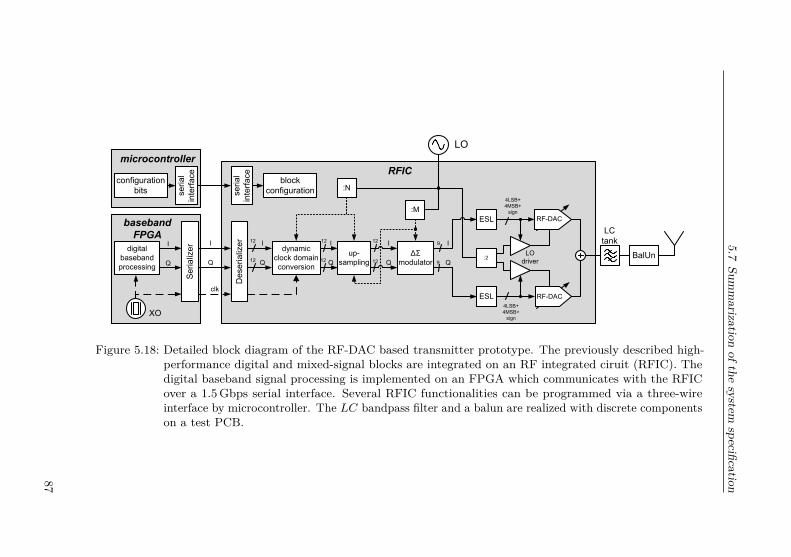
5.7Sum
marization
ofthesystem
specification
LC
tank
LO
:2
dynamic
clock domain
conversion
:N
up-
sampling
digital
baseband
processing
Se
ria
lize
r
XO
De
se
ria
lize
r
clk
:M
ΔΣ
modulator
microcontroller
RFIC
12
12
LO
driver
se
ria
l
inte
rfa
ce
se
ria
l
inte
rfa
ce
configuration
bits
block
configuration
12
12
12
12
RF-DAC
9
9
ESL
ESL RF-DAC
I
Q
I
Q
I
Q
I
Q
I
Q
4LSB+
4MSB+
sign
4LSB+
4MSB+
sign
I
QBalUn
baseband
FPGA
Figure 5.18: Detailed block diagram of the RF-DAC based transmitter prototype. The previously described high-performance digital and mixed-signal blocks are integrated on an RF integrated ciruit (RFIC). Thedigital baseband signal processing is implemented on an FPGA which communicates with the RFICover a 1.5Gbps serial interface. Several RFIC functionalities can be programmed via a three-wireinterface by microcontroller. The LC bandpass filter and a balun are realized with discrete componentson a test PCB.
87

88
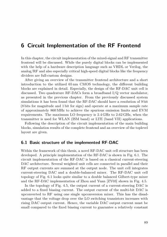
6 Circuit Implementation of the RF Frontend
In this chapter, the circuit implementation of the mixed-signal and RF transmitterfrontend will be discussed. While the purely digital blocks can be implementedwith the help of a hardware description language such as VHDL or Verilog, theanalog/RF and also especially critical high-speed digital blocks like the frequencydividers are full-custom designs.
After giving an overview of the transmitter frontend architecture and a shortintroduction to the utilized 65 nm CMOS technology, the different buildingblocks are explained in detail. Especially, the design of the RF-DAC unit cell isdiscussed. Two quadrature RF-DACs form a broadband I/Q vector modulator,as presented in the previous chapter. From the previously discussed systemsimulations it has been found that the RF-DAC should have a resolution of 9 bit(8 bits for magnitude and 1 bit for sign) and operate at a maximum sample rateof approximately 860MHz to achieve the spurious emission limits and EVMrequirements. The maximum LO frequency is 2.4GHz to 2.62GHz, when thetransmitter is used for WLAN (ISM band) or LTE (band VII) applications.Following the description of the circuit implementation of the main building
blocks, simulation results of the complete frontend and an overview of the toplevellayout are given.
6.1 Basic structure of the implemented RF-DAC
Within the framework of this thesis, a novel RF-DAC unit cell structure has beendeveloped. A principle implementation of the RF-DAC is shown in Fig. 6.1. Thecircuit implementation of the RF-DAC is based on a classical current-steeringDAC architecture. Several weighted unit cells are connected in parallel and theirRF output currents are summed at the output node. The unit cell integratescurrent-steering DAC and a double-balanced mixer. The RF-DAC unit celltopology of Fig. 6.1 looks quite similar to a double balanced Gilbert-type mixerand the RF-DAC implementation of Zhou and Yuan [ZY03] shown in Fig. 4.5.In the topology of Fig. 4.5, the output current of a current-steering DAC is
added to a fixed biasing current. The output current of the multi-bit DAC isupconverted to RF using one single upconversion mixer. This has the disad-vantage that the voltage drop over the LO switching transistors increases withrising DAC output current. Hence, the variable DAC output current must besmall compared to the fixed biasing current to guarantee a relatively constant
89
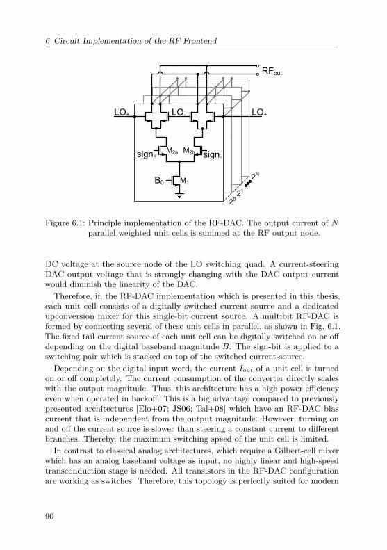
6 Circuit Implementation of the RF Frontend
B1
sign-
B1
sign-
B1
sign-
RFout
LO+
2021
2N
LO+
B0
LO-
sign-sign+M2a M2b
M1
Figure 6.1: Principle implementation of the RF-DAC. The output current of Nparallel weighted unit cells is summed at the RF output node.
DC voltage at the source node of the LO switching quad. A current-steeringDAC output voltage that is strongly changing with the DAC output currentwould diminish the linearity of the DAC.
Therefore, in the RF-DAC implementation which is presented in this thesis,each unit cell consists of a digitally switched current source and a dedicatedupconversion mixer for this single-bit current source. A multibit RF-DAC isformed by connecting several of these unit cells in parallel, as shown in Fig. 6.1.The fixed tail current source of each unit cell can be digitally switched on or offdepending on the digital baseband magnitude B. The sign-bit is applied to aswitching pair which is stacked on top of the switched current-source.
Depending on the digital input word, the current Iout of a unit cell is turnedon or off completely. The current consumption of the converter directly scaleswith the output magnitude. Thus, this architecture has a high power efficiencyeven when operated in backoff. This is a big advantage compared to previouslypresented architectures [Elo+07; JS06; Tal+08] which have an RF-DAC biascurrent that is independent from the output magnitude. However, turning onand off the current source is slower than steering a constant current to differentbranches. Thereby, the maximum switching speed of the unit cell is limited.
In contrast to classical analog architectures, which require a Gilbert-cell mixerwhich has an analog baseband voltage as input, no highly linear and high-speedtransconduction stage is needed. All transistors in the RF-DAC configurationare working as switches. Therefore, this topology is perfectly suited for modern
90
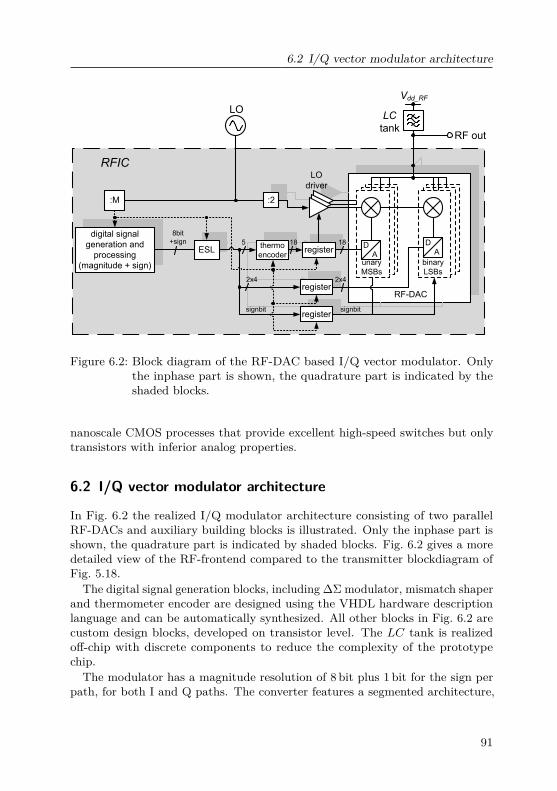
6.2 I/Q vector modulator architecture
LC
tank
Vdd_RF
LO
5
:2:M
thermo
encoderregister
18 18D
A
binary
LSBs
DA
binary
LSBs
DA
binary
LSBs
DA
binary
LSBs
RF-DAC
LO
driver
digital signal
generation and
processing
(magnitude + sign)
RF out
8bit
+sign
register
register2x4
signbit
2x4
signbit
D
Aunary
MSBs
D
A
binary
LSBs
ESL
8bit
+sign
RFIC
Figure 6.2: Block diagram of the RF-DAC based I/Q vector modulator. Onlythe inphase part is shown, the quadrature part is indicated by theshaded blocks.
nanoscale CMOS processes that provide excellent high-speed switches but onlytransistors with inferior analog properties.
6.2 I/Q vector modulator architecture
In Fig. 6.2 the realized I/Q modulator architecture consisting of two parallelRF-DACs and auxiliary building blocks is illustrated. Only the inphase part isshown, the quadrature part is indicated by shaded blocks. Fig. 6.2 gives a moredetailed view of the RF-frontend compared to the transmitter blockdiagram ofFig. 5.18.
The digital signal generation blocks, including ∆Σ modulator, mismatch shaperand thermometer encoder are designed using the VHDL hardware descriptionlanguage and can be automatically synthesized. All other blocks in Fig. 6.2 arecustom design blocks, developed on transistor level. The LC tank is realizedoff-chip with discrete components to reduce the complexity of the prototypechip.
The modulator has a magnitude resolution of 8 bit plus 1 bit for the sign perpath, for both I and Q paths. The converter features a segmented architecture,
91
6 Circuit Implementation of the RF Frontend
0 0.2 0.4 0.6 0.8 1 1.2 1.4 1.6 1.8 20
1
2
3
4
5
6
7
8
9
10
Vds [V]
Id [m
A]
Vgs=0.4VVgs=0.6VVgs=0.8VVgs=1.0VVgs=1.2VVgs=1.4VVgs=1.6VVgs=1.8VVgs=2.0V
Figure 6.3: NMOS I-V device characteristics for a 60 nm gatelength transistorwith an aspect ratio of 100.
the 4 least significant bits (LSBs) are realized as binary weighted cells, whilethe most significant bits (MSBs) are realized as unary weighted cells. Thereby,glitches are reduced while retaining a reasonably low complexity for wiring andcontrol logic [Pla03]. A thermometer encoder is utilized to convert the MSBsfrom binary to unary representation. The thermometer encoder functionality isincluded in the element selection logic (ESL) block (see section 5.5.3).The implementation of the LO buffers that amplify the LO carrier signal
and drive the LO switching quads of the RF-DAC unit cells is based on aninverter chain. Each MSB unit cell has its own buffer. To save power, a buffercan be deactivated if the corresponding RF-DAC unit cell is also inactive. Theimplementation of the LO driver chain is described in section 6.5.Registers are used to synchronize the switching of all blocks with a common
clock signal. Also, they act as driver circuit for the RF-DAC switches. Theregisters consist of two consecutive latches. Details on the implementation ofthe latches can found in section 6.6.
6.3 Survey of the utilized 65 nm CMOS technology
The RF-DAC transmitter has been implemented in TSMC’s CMN65LP 65 nmCMOS technology. The technology is optimized for low power consumption of
92
6.4 Implementation details of the RF-DAC unit cell
digital circuits. It features three different thin gate-oxide transistor types withstandard, high and low threshold voltage. The thin gate-oxide transistors arecompatible to 1.2V supply voltage. In addition it provides thick gate-oxidetransistors for I/O devices which are compatible to a supply voltage of 2.5V.The technology features one polysilicon and nine metal layers that are madeof copper. The top metal layer has a thickness of 3.4µm. Capacitors can berealized using the MIM-capacitor option with a capacitance density of 2 fF/µm2.A deep N-well option allows to place sensitive circuits in their own well with anisolated substrate contact.In Fig. 6.3 the I-V device characteristics of an NMOS transistor with 60 nm
gate length are shown. Short channel effects of the nanoscale CMOS transistorsare very evident. The drain current only increases linearly with increasinggate-source voltage, instead of the classical quadratic behavior which can beobserved for long-channel transistors. Also, the output resistance of the 60 nmtransistors is very low, leading to a strong dependence of the drain current onthe drain-source voltage.
6.4 Implementation details of the RF-DAC unit cell
Fig 6.1 shows a simplified schematic of the implemented RF-DAC unit cell. Thebiasing and control circuitry of the current source and sign function are notdepicted. The current output DAC, which is controlled by the digital basebandinput signal, consists of a switched tail current source M1 and a transistor pairM2a andM2b which is stacked on top of the current source and steers the currentto the positive or negative output, depending on the sign-bit of the digital inputsignal. The sign-bit changes relatively seldom compared to the sampling rate ofthe DAC. Therefore, the transistor pair acts as a cascode for the tail currentsource transistor. The cascode configuration has a very high output resistance,thereby minimizing the sensitivity of the output current to variations of theoutput voltage.
The control voltages of the transistors M1, M2a and M2b have to be switchedbetween zero and some biasing voltage, which allows optimum performance ofthe RF-DAC. Subsequently, an optimum biasing strategy for the RF-DAC unitcell is developed.
6.4.1 Biasing of the unit cell
The best way to accurately define the output current of each unit cell is bymeans of a current mirror. As the transistors M2a and M2b act as cascodesfor M1, a cascode current mirror is the topology of choice. Fig. 6.4(a) shows asimple cascode current mirror configuration. For finding the optimum biasing of
93
6 Circuit Implementation of the RF Frontend
M2
M1M3
M4
Vout
Iout
Iin
VDD
Vt+Vov
2(Vt+Vov)
Vin
(a) Cascode current mirror
vout
iout
vds1=-vgs2=-vbs2
gm2vgs2 rds2 gmb2vbs2
rds1
(b) Small signal equivalent circuit of M1 and M2
Figure 6.4: Cascode current mirror and its small signal equivalent circuit todetermine rout.
the transistors of the output brach, the transistor pair M2a and M2b is treatedas a single transistor M2.
Cascode current mirror
To achieve a high linearity of the current-output DAC, the output currentshould be as independent as possible from the output voltage. Thus, the outputresistance of the current mirror must be maximized. The small signal equivalentcircuit for determining the output resistance rout of the output branch, consistingof M1 and M2, is shown in Fig. 6.4(b). From this equivalent circuit the (smallsignal) output resistance of the cascode current mirror can be found as
rout = voutiout
∣∣∣vg1=vg2=0
= rds2 [1 + (gm2 + gmb2)rds1] + rds1. (6.1)
The output resistance of a cascode current mirror has an output resistance whichis much higher compared to a simple current mirror. Adding a cascode transistorincreases rout approximately by a factor of (1 + gm2rds2).Furthermore, it can be observed that the output resistance increases, when
the (large signal) output current decreases. This, however, also decreases themaximum operation speed [Gra+01, p. 254].
To function properly, all transistors of the current mirror have to be operatedin the active (saturated) region. This limits the minimum input voltage Vin,min
94
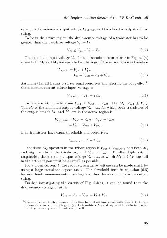
6.4 Implementation details of the RF-DAC unit cell
as well as the minimum output voltage Vout,min and therefore the output voltageswing.To be in the active region, the drain-source voltage of a transistor has to be
greater than the overdrive voltage Vgs − Vt:
Vds ≥ Vgs − Vt = Vov. (6.2)
The minimum input voltage Vin for the cascode current mirror in Fig. 6.4(a)where both M3 and M4 are operated at the edge of the active region is therefore
Vin,min = Vgs3 + Vgs4
= Vt3 + Vov3 + Vt4 + Vov4. (6.3)
Assuming that all transistors have equal overdrives and ignoring the body effect1,the minimum current mirror input voltage is
Vin,min = 2Vt + 2Vov. (6.4)
To operate M1 in saturation Vds1 ≈ Vds3 = Vgs3. For M2, Vds2 ≥ Vov2.Therefore, the minimum output voltage Vout,min for which both transistors ofthe output branch M1 and M2 are in the active region is
Vout,min = Vds1 + Vov2 = Vgs3 + Vov2
= Vt3 + Vov3 + Vov2. (6.5)
If all transistors have equal thresholds and overdrives,
Vout,min = Vt + 2Vov. (6.6)
Transistor M2 operates in the triode region if Vout < Vout,min and both M1and M2 operate in the triode region if Vout < Vov1. To allow high outputamplitudes, the minimum output voltage Vout,min at which M1 and M2 are stillin the active region must be as small as possible.For a given current I, the required overdrive voltage can be made small by
using a large transistor aspect ratio. The threshold term in equation (6.6)however limits minimum output voltage and thus the maximum possible outputswing.Further investigating the circuit of Fig. 6.4(a), it can be found that the
drain-source voltage of M1 is
Vds1 = Vin − Vgs2 = Vt + Vov. (6.7)1The body-effect further increases the threshold of all transistors with VSB > 0. In the
cascode current mirror of Fig. 6.4(a) the transistors M4 and M2 would be effected, as faras they are not placed in their own p-well.
95
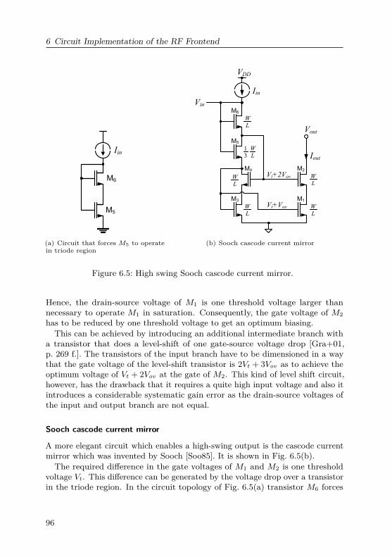
6 Circuit Implementation of the RF Frontend
M6
M5
Iin
(a) Circuit that forces M5 to operatein triode region
M1
M2
Iout
WL
WL
M3
M4
WL
WL
M5
M6
WL
WL
1
3
Iin
Vout
VDD
Vin
Vt+Vov
Vt+2Vov
(b) Sooch cascode current mirror
Figure 6.5: High swing Sooch cascode current mirror.
Hence, the drain-source voltage of M1 is one threshold voltage larger thannecessary to operate M1 in saturation. Consequently, the gate voltage of M2has to be reduced by one threshold voltage to get an optimum biasing.This can be achieved by introducing an additional intermediate branch with
a transistor that does a level-shift of one gate-source voltage drop [Gra+01,p. 269 f.]. The transistors of the input branch have to be dimensioned in a waythat the gate voltage of the level-shift transistor is 2Vt + 3Vov as to achieve theoptimum voltage of Vt + 2Vov at the gate of M2. This kind of level shift circuit,however, has the drawback that it requires a quite high input voltage and also itintroduces a considerable systematic gain error as the drain-source voltages ofthe input and output branch are not equal.
Sooch cascode current mirror
A more elegant circuit which enables a high-swing output is the cascode currentmirror which was invented by Sooch [Soo85]. It is shown in Fig. 6.5(b).The required difference in the gate voltages of M1 and M2 is one threshold
voltage Vt. This difference can be generated by the voltage drop over a transistorin the triode region. In the circuit topology of Fig. 6.5(a) transistor M6 forces
96
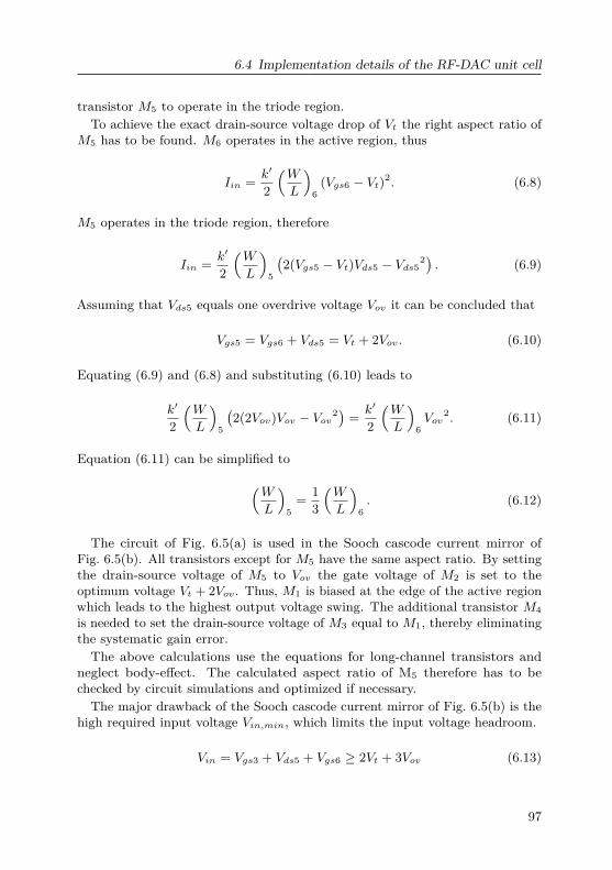
6.4 Implementation details of the RF-DAC unit cell
transistor M5 to operate in the triode region.To achieve the exact drain-source voltage drop of Vt the right aspect ratio of
M5 has to be found. M6 operates in the active region, thus
Iin = k′
2
(W
L
)6
(Vgs6 − Vt)2. (6.8)
M5 operates in the triode region, therefore
Iin = k′
2
(W
L
)5
(2(Vgs5 − Vt)Vds5 − Vds5
2) . (6.9)
Assuming that Vds5 equals one overdrive voltage Vov it can be concluded that
Vgs5 = Vgs6 + Vds5 = Vt + 2Vov. (6.10)
Equating (6.9) and (6.8) and substituting (6.10) leads to
k′
2
(W
L
)5
(2(2Vov)Vov − Vov2) = k′
2
(W
L
)6Vov
2. (6.11)
Equation (6.11) can be simplified to(W
L
)5
= 13
(W
L
)6. (6.12)
The circuit of Fig. 6.5(a) is used in the Sooch cascode current mirror ofFig. 6.5(b). All transistors except for M5 have the same aspect ratio. By settingthe drain-source voltage of M5 to Vov the gate voltage of M2 is set to theoptimum voltage Vt + 2Vov. Thus, M1 is biased at the edge of the active regionwhich leads to the highest output voltage swing. The additional transistor M4is needed to set the drain-source voltage of M3 equal to M1, thereby eliminatingthe systematic gain error.The above calculations use the equations for long-channel transistors and
neglect body-effect. The calculated aspect ratio of M5 therefore has to bechecked by circuit simulations and optimized if necessary.
The major drawback of the Sooch cascode current mirror of Fig. 6.5(b) is thehigh required input voltage Vin,min, which limits the input voltage headroom.
Vin = Vgs3 + Vds5 + Vgs6 ≥ 2Vt + 3Vov (6.13)
97
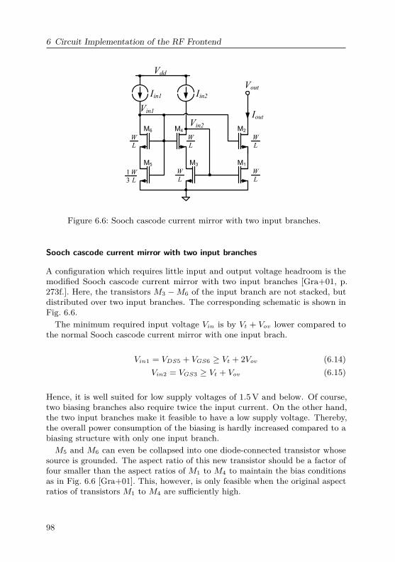
6 Circuit Implementation of the RF Frontend
M1
M2
Iout
WL
WL
Vin1
M3
M4
WL
WL
M5
M6
Iin2
WL
WL
1
3
Iin1
Vin2
Vout
Vdd
Figure 6.6: Sooch cascode current mirror with two input branches.
Sooch cascode current mirror with two input branches
A configuration which requires little input and output voltage headroom is themodified Sooch cascode current mirror with two input branches [Gra+01, p.273f.]. Here, the transistors M3 −M6 of the input branch are not stacked, butdistributed over two input branches. The corresponding schematic is shown inFig. 6.6.The minimum required input voltage Vin is by Vt + Vov lower compared to
the normal Sooch cascode current mirror with one input brach.
Vin1 = VDS5 + VGS6 ≥ Vt + 2Vov (6.14)Vin2 = VGS3 ≥ Vt + Vov (6.15)
Hence, it is well suited for low supply voltages of 1.5V and below. Of course,two biasing branches also require twice the input current. On the other hand,the two input branches make it feasible to have a low supply voltage. Thereby,the overall power consumption of the biasing is hardly increased compared to abiasing structure with only one input branch.M5 and M6 can even be collapsed into one diode-connected transistor whose
source is grounded. The aspect ratio of this new transistor should be a factor offour smaller than the aspect ratios of M1 to M4 to maintain the bias conditionsas in Fig. 6.6 [Gra+01]. This, however, is only feasible when the original aspectratios of transistors M1 to M4 are sufficiently high.
98
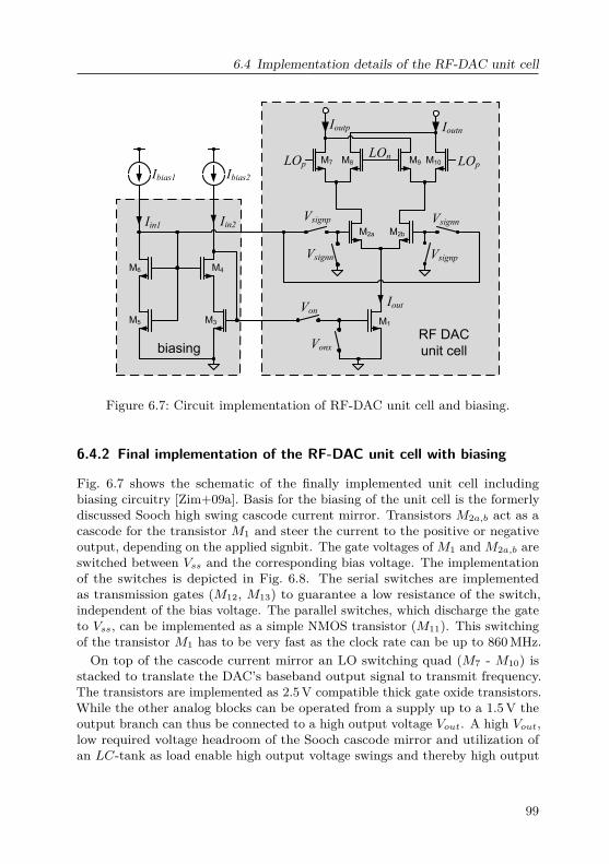
6.4 Implementation details of the RF-DAC unit cell
M3
M4
M5
M6
VsignpVsignn
Vsignp Vsignn
VonM1
M2bM2a
VonxRF DAC
unit cell
Iout
Iin1 Iin2
LOnLOp LOp
Ioutp Ioutn
M7 M8 M9 M10
biasing
Ibias1 Ibias2
Figure 6.7: Circuit implementation of RF-DAC unit cell and biasing.
6.4.2 Final implementation of the RF-DAC unit cell with biasing
Fig. 6.7 shows the schematic of the finally implemented unit cell includingbiasing circuitry [Zim+09a]. Basis for the biasing of the unit cell is the formerlydiscussed Sooch high swing cascode current mirror. Transistors M2a,b act as acascode for the transistor M1 and steer the current to the positive or negativeoutput, depending on the applied signbit. The gate voltages ofM1 andM2a,b areswitched between Vss and the corresponding bias voltage. The implementationof the switches is depicted in Fig. 6.8. The serial switches are implementedas transmission gates (M12, M13) to guarantee a low resistance of the switch,independent of the bias voltage. The parallel switches, which discharge the gateto Vss, can be implemented as a simple NMOS transistor (M11). This switchingof the transistor M1 has to be very fast as the clock rate can be up to 860MHz.On top of the cascode current mirror an LO switching quad (M7 - M10) is
stacked to translate the DAC’s baseband output signal to transmit frequency.The transistors are implemented as 2.5V compatible thick gate oxide transistors.While the other analog blocks can be operated from a supply up to a 1.5V theoutput branch can thus be connected to a high output voltage Vout. A high Vout,low required voltage headroom of the Sooch cascode mirror and utilization ofan LC-tank as load enable high output voltage swings and thereby high output
99
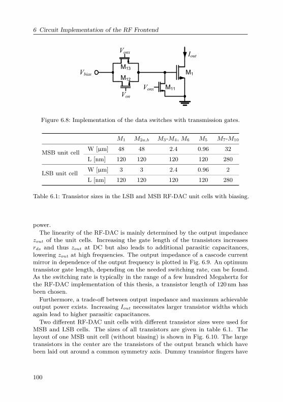
6 Circuit Implementation of the RF Frontend
M13
M12
M11
M1
Iout
Vonx
Vbias
Vonx
Von
Figure 6.8: Implementation of the data switches with transmission gates.
M1 M2a,b M3-M4, M6 M5 M7-M10
MSB unit cell W [µm] 48 48 2.4 0.96 32L [nm] 120 120 120 120 280
LSB unit cell W [µm] 3 3 2.4 0.96 2L [nm] 120 120 120 120 280
Table 6.1: Transistor sizes in the LSB and MSB RF-DAC unit cells with biasing.
power.The linearity of the RF-DAC is mainly determined by the output impedance
zout of the unit cells. Increasing the gate length of the transistors increasesrds and thus zout at DC but also leads to additional parasitic capacitances,lowering zout at high frequencies. The output impedance of a cascode currentmirror in dependence of the output frequency is plotted in Fig. 6.9. An optimumtransistor gate length, depending on the needed switching rate, can be found.As the switching rate is typically in the range of a few hundred Megahertz forthe RF-DAC implementation of this thesis, a transistor length of 120 nm hasbeen chosen.
Furthermore, a trade-off between output impedance and maximum achievableoutput power exists. Increasing Iout necessitates larger transistor widths whichagain lead to higher parasitic capacitances.Two different RF-DAC unit cells with different transistor sizes were used for
MSB and LSB cells. The sizes of all transistors are given in table 6.1. Thelayout of one MSB unit cell (without biasing) is shown in Fig. 6.10. The largetransistors in the center are the transistors of the output branch which havebeen laid out around a common symmetry axis. Dummy transistor fingers have
100
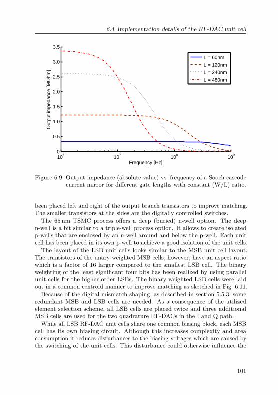
6.4 Implementation details of the RF-DAC unit cell
106 107 108 1090
0.5
1.0
1.5
2.0
2.5
3.0
3.5
Frequency [Hz]
Out
put i
mpe
danc
e [M
Ohm
]
L = 60nm
L = 120nm
L = 240nm
L = 480nm
Figure 6.9: Output impedance (absolute value) vs. frequency of a Sooch cascodecurrent mirror for different gate lengths with constant (W/L) ratio.
been placed left and right of the output branch transistors to improve matching.The smaller transistors at the sides are the digitally controlled switches.
The 65 nm TSMC process offers a deep (buried) n-well option. The deepn-well is a bit similar to a triple-well process option. It allows to create isolatedp-wells that are enclosed by an n-well around and below the p-well. Each unitcell has been placed in its own p-well to achieve a good isolation of the unit cells.The layout of the LSB unit cells looks similar to the MSB unit cell layout.
The transistors of the unary weighted MSB cells, however, have an aspect ratiowhich is a factor of 16 larger compared to the smallest LSB cell. The binaryweighting of the least significant four bits has been realized by using parallelunit cells for the higher order LSBs. The binary weighted LSB cells were laidout in a common centroid manner to improve matching as sketched in Fig. 6.11.Because of the digital mismatch shaping, as described in section 5.5.3, some
redundant MSB and LSB cells are needed. As a consequence of the utilizedelement selection scheme, all LSB cells are placed twice and three additionalMSB cells are used for the two quadrature RF-DACs in the I and Q path.
While all LSB RF-DAC unit cells share one common biasing block, each MSBcell has its own biasing circuit. Although this increases complexity and areaconsumption it reduces disturbances to the biasing voltages which are caused bythe switching of the unit cells. This disturbance could otherwise influence the
101
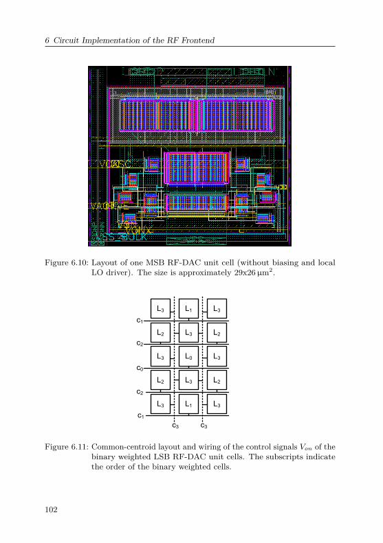
6 Circuit Implementation of the RF Frontend
Figure 6.10: Layout of one MSB RF-DAC unit cell (without biasing and localLO driver). The size is approximately 29x26µm2.
L0
L3
L3
L1
L1
L3
L2
L3
L2
L3
L3
L2
L3
L2
L3
c0
c2
c1c3 c3
c2
c1
Figure 6.11: Common-centroid layout and wiring of the control signals Von of thebinary weighted LSB RF-DAC unit cells. The subscripts indicatethe order of the binary weighted cells.
102
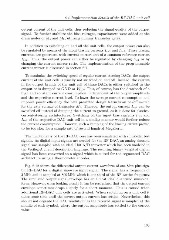
6.4 Implementation details of the RF-DAC unit cell
output current of the unit cells, thus reducing the signal quality of the outputsignal. To further stabilize the bias voltages, capacitances were added at thedrain nodes of M4 and M6, utilizing dummy transistor gates.
In addition to switching on and off the unit cells, the output power can alsobe regulated by means of the input biasing currents Iin1 and Iin2. These biasingcurrents are generated with current mirrors out of a common reference currentIref . Thus, the output power can either be regulated by changing Iref or bychanging the current mirror ratio. The implementation of the programmablecurrent mirror is discussed in section 6.7.
To maximize the switching speed of regular current steering DACs, the outputcurrent of the unit cells is usually not switched on and off. Instead, the currentin the output branch of the unit cell of these DACs is either switched to theoutput or is dumped to GND or VDD. This, of course, has the drawback of ahigh and constant current consumption, independent of the output amplitudeand the respective current level. To lower the average current consumption andimprove power efficiency the here presented design features an on/off switchfor the gate voltage of transistor M1. Thereby, the output current Iout can beswitched off instead of dumping the current to ground, as it is done for classicalcurrent-steering architectures. Switching off the input bias currents Iin1 andIin2 of the respective DAC unit cell in a similar manner would further reducethe current consumption. However, such a ramping of the biasing circuit provedto be too slow for a sample rate of several hundred Megahertz.
The functionality of the RF-DAC core has been simulated with sinusoidal testsignals. As digital input signals are needed for the RF-DAC, an analog sinusoidsignal was sampled with an ideal 9 bit A/D converter which has been modeled inthe Verilog-A circuit description language. The resulting binary weighted digitalsignal has been converted to a signal which is suited for the segmented DACarchitecture using a thermometer encoder.
Fig. 6.12 shows the differential output current waveform of one 8 bit plus sign-bit RF-DAC for a digital sinewave input signal. The signal has a frequency of2MHz and is sampled at 800MHz which is one third of the RF carrier frequency.The simulated output signal envelope has an almost ideal quantized sinusoidalform. However, when looking closely it can be recognized that the output currentenvelope sometimes drops slightly for a short moment. This is caused whenadditional RF-DAC unit cells are activated. When switching on a unit cell ittakes some time until the correct output current has settled. Nevertheless, thisshould not degrade the DAC resolution, as the received signal is sampled at themiddle of each symbol, where the output amplitude has settled to the correctvalue.
103
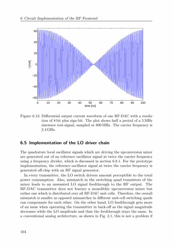
6 Circuit Implementation of the RF Frontend
0 10 20 30 40 50 60 70 80 90 100
−60
−40
−20
0
20
40
60
time [ns]
I [m
A]
Figure 6.12: Differential output current waveform of one RF-DAC with a resolu-tion of 8 bit plus sign-bit. The plot shows half a period of a 5MHzsinewave test-signal, sampled at 800MHz. The carrier frequency is2.4GHz.
6.5 Implementation of the LO driver chain
The quadrature local oscillator signals which are driving the upconversion mixerare generated out of an reference oscillator signal at twice the carrier frequencyusing a frequency divider, which is discussed in section 6.8.1. For the prototypeimplementation, the reference oscillator signal at twice the carrier frequency isgenerated off-chip with an RF signal generator.In every transmitter, the LO switch drivers amount perceptible to the total
power consumption. Also, mismatch in the switching quad transistors of themixer leads to an unwanted LO signal feedthrough to the RF output. TheRF-DAC transmitter does not feature a monolithic upconversion mixer butrather one which is distributed over all RF-DAC unit cells. Therefore, the overallmismatch is smaller as opposed mismatches in different unit-cell switching quadscan compensate for each other. On the other hand, LO feedthrough gets moreof an issue when operating the transmitter in back-off as the signal magnitudedecreases while the LO amplitude and thus the feedthrough stays the same. Ina conventional analog architecture, as shown in Fig. 2.1, this is not a problem if
104
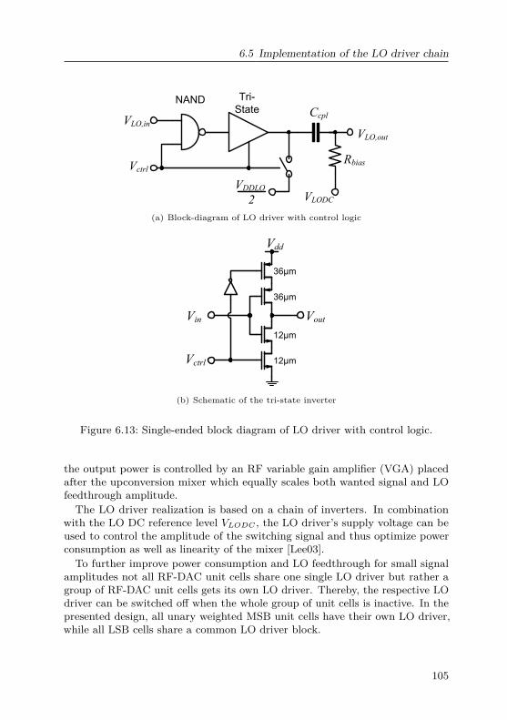
6.5 Implementation of the LO driver chain
NAND Tri-
StateVLO,in
Vctrl
VDDLO2
Ccpl
VLODC
VLO,out
Rbias
(a) Block-diagram of LO driver with control logic
Vout
Vdd
36μm
36μm
12μm
12μm
Vin
Vctrl
(b) Schematic of the tri-state inverter
Figure 6.13: Single-ended block diagram of LO driver with control logic.
the output power is controlled by an RF variable gain amplifier (VGA) placedafter the upconversion mixer which equally scales both wanted signal and LOfeedthrough amplitude.The LO driver realization is based on a chain of inverters. In combination
with the LO DC reference level VLODC , the LO driver’s supply voltage can beused to control the amplitude of the switching signal and thus optimize powerconsumption as well as linearity of the mixer [Lee03].To further improve power consumption and LO feedthrough for small signal
amplitudes not all RF-DAC unit cells share one single LO driver but rather agroup of RF-DAC unit cells gets its own LO driver. Thereby, the respective LOdriver can be switched off when the whole group of unit cells is inactive. In thepresented design, all unary weighted MSB unit cells have their own LO driver,while all LSB cells share a common LO driver block.
105
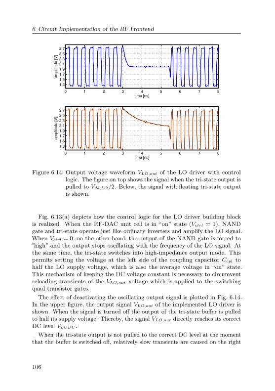
6 Circuit Implementation of the RF Frontend
0 1 2 3 4 5 6 7 8
1.3
1.5
1.7
1.9
2.1
2.3
2.5
2.7
time [ns]
am
plit
ud
e [
V]
0 1 2 3 4 5 6 7 8
1.3
1.5
1.7
1.9
2.1
2.3
2.5
2.7
time [ns]
am
plit
ud
e [
V]
Figure 6.14: Output voltage waveform VLO,out of the LO driver with controllogic. The figure on top shows the signal when the tri-state output ispulled to Vdd,LO/2. Below, the signal with floating tri-state outputis shown.
Fig. 6.13(a) depicts how the control logic for the LO driver building blockis realized. When the RF-DAC unit cell is in “on” state (Vctrl = 1), NANDgate and tri-state operate just like ordinary inverters and amplify the LO signal.When Vctrl = 0, on the other hand, the output of the NAND gate is forced to“high” and the output stops oscillating with the frequency of the LO signal. Atthe same time, the tri-state switches into high-impedance output mode. Thispermits setting the voltage at the left side of the coupling capacitor Ccpl tohalf the LO supply voltage, which is also the average voltage in “on” state.This mechanism of keeping the DC voltage constant is necessary to circumventreloading transients of the VLO,out voltage which is applied to the switchingquad transistor gates.
The effect of deactivating the oscillating output signal is plotted in Fig. 6.14.In the upper figure, the output signal VLO,out of the implemented LO driver isshown. When the signal is turned off the output of the tri-state buffer is pulledto half its supply voltage. Thereby, the signal VLO,out directly reaches its correctDC level VLODC .
When the tri-state output is not pulled to the correct DC level at the momentthat the buffer is switched off, relatively slow transients are caused on the right
106
6.6 Implementation of the latches and registers
hand side of the coupling capacitor Ccpl. This is depicted in the bottom picture.Thus, the DC level may not identical to VLODC when the LO driver is switchedon again. In Fig. 6.14 this shift in DC level is roughly 60mV. It is much worsewhen the off-period of the LO driver is shorter. The inverted LO driver signalVLOn experiences a similar transient, but with a phase-shift of 180°. Thereby,the difference between DC voltage levels of the VLOp and VLOn signals for theexample of Fig. 6.14 is approximately 120mV when switching on the LO drivers,leading to distortions of the output signal.
The logic operation of the tri-state is the same as of a combination of tri-stateplus NAND gate. Anyhow, without the NAND gate preceding the tri-state theRF signal input of the tri-state would be always active, leading to a considerablefeedthrough of the LO signal to the output node VLO,out even if the tri-state isswitched to high-impedance output mode.As the transistors of the LO switching quad in the RF-DAC are relatively
large, quite big coupling capacitors Ccpl are needed. These coupling capacitorsare realized as MIM-capacitors. Each capacitor Ccpl has a size of 1.8 pF. To savechip area, the coupling capacitors have placed in the higher metal layers abovethe active RF-DAC circuitry in the layout.
6.6 Implementation of the latches and registers
Registers are used to synchronize the switching of all RF-DAC unit cells. Inaddition, they act as driver circuit for the RF-DAC switches. The registers consistof two consecutive latches. For a good RF-DAC performance the latches have tobe designed in a way that the RF-DAC’s serial and parallel switch transistors(M11 - M13 in Fig. 6.8) are not on at the same time. Otherwise, a current wouldflow from the biasing branches to Vss, decharging the bias voltage nodes Vbias.On the other hand, the transistors also should not simultaneously be turnedoff for a too long time. To make sure that both switches are simultaneouslyin the off-state for a short instance, the rising edge of the control signal Vonxshould not go up until the falling edge of Von has occurred. In other words, thecrossover point of these two signals has to be at a low amplitude.
A differential latch as presented by Bosch et al. [Bos+01] has been used for thispurpose. The schematic of the latch is depicted in Fig. 6.15. This type of latchcan achieve a very high speed operation. Also, it allows to set the crossover pointof the control signals by using different rise and fall times for the differentialoutput of the latch. The rise and fall time of the output signals can be controlledby changing the width ratio of the PMOS to NMOS transistors. If the ratio issimilar to the µp/µn electron mobility ratio, the crossover point is located athalf the supply voltage. In addition, the cross coupled NMOS transistors M5and M6 increase the decharging speed, thus lowering the crossover points.
107
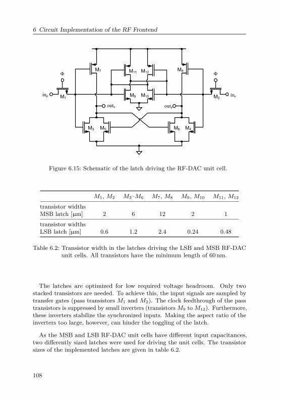
6 Circuit Implementation of the RF Frontend
F
inp
F
inn
outn outp
M1 M2
M3 M4M5 M6
M7 M8
M9 M10
M11 M12
Figure 6.15: Schematic of the latch driving the RF-DAC unit cell.
M1, M2 M3–M6 M7, M8 M9, M10 M11, M12
transistor widthsMSB latch [µm] 2 6 12 2 1transistor widthsLSB latch [µm] 0.6 1.2 2.4 0.24 0.48
Table 6.2: Transistor width in the latches driving the LSB and MSB RF-DACunit cells. All transistors have the minimum length of 60 nm.
The latches are optimized for low required voltage headroom. Only twostacked transistors are needed. To achieve this, the input signals are sampled bytransfer gates (pass transistors M1 and M2). The clock feedthrough of the passtransistors is suppressed by small inverters (transistorsM9 toM12). Furthermore,these inverters stabilize the synchronized inputs. Making the aspect ratio of theinverters too large, however, can hinder the toggling of the latch.
As the MSB and LSB RF-DAC unit cells have different input capacitances,two differently sized latches were used for driving the unit cells. The transistorsizes of the implemented latches are given in table 6.2.
108
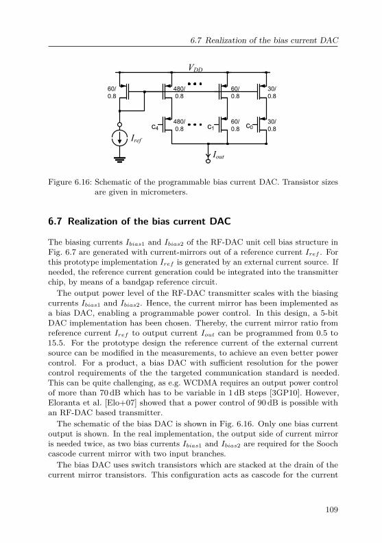
6.7 Realization of the bias current DAC
60/
0.8
30/
0.8
60/
0.8
480/
0.8
30/
0.8
60/
0.8
480/
0.8
Iref
Iout
c0c1c4
VDD
Figure 6.16: Schematic of the programmable bias current DAC. Transistor sizesare given in micrometers.
6.7 Realization of the bias current DAC
The biasing currents Ibias1 and Ibias2 of the RF-DAC unit cell bias structure inFig. 6.7 are generated with current-mirrors out of a reference current Iref . Forthis prototype implementation Iref is generated by an external current source. Ifneeded, the reference current generation could be integrated into the transmitterchip, by means of a bandgap reference circuit.The output power level of the RF-DAC transmitter scales with the biasing
currents Ibias1 and Ibias2. Hence, the current mirror has been implemented asa bias DAC, enabling a programmable power control. In this design, a 5-bitDAC implementation has been chosen. Thereby, the current mirror ratio fromreference current Iref to output current Iout can be programmed from 0.5 to15.5. For the prototype design the reference current of the external currentsource can be modified in the measurements, to achieve an even better powercontrol. For a product, a bias DAC with sufficient resolution for the powercontrol requirements of the the targeted communication standard is needed.This can be quite challenging, as e.g. WCDMA requires an output power controlof more than 70 dB which has to be variable in 1 dB steps [3GP10]. However,Eloranta et al. [Elo+07] showed that a power control of 90 dB is possible withan RF-DAC based transmitter.The schematic of the bias DAC is shown in Fig. 6.16. Only one bias current
output is shown. In the real implementation, the output side of current mirroris needed twice, as two bias currents Ibias1 and Ibias2 are required for the Soochcascode current mirror with two input branches.The bias DAC uses switch transistors which are stacked at the drain of the
current mirror transistors. This configuration acts as cascode for the current
109
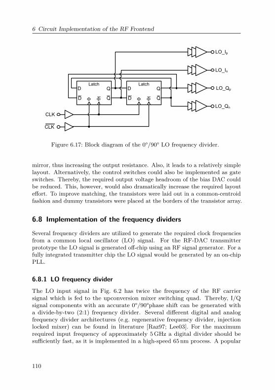
6 Circuit Implementation of the RF Frontend
LatchD Q
FD QF
LatchD Q
FD QF
CLK
CLK
LO_Ip
LO_In
LO_Qp
LO_Qn
Figure 6.17: Block diagram of the 0°/90° LO frequency divider.
mirror, thus increasing the output resistance. Also, it leads to a relatively simplelayout. Alternatively, the control switches could also be implemented as gateswitches. Thereby, the required output voltage headroom of the bias DAC couldbe reduced. This, however, would also dramatically increase the required layouteffort. To improve matching, the transistors were laid out in a common-centroidfashion and dummy transistors were placed at the borders of the transistor array.
6.8 Implementation of the frequency dividers
Several frequency dividers are utilized to generate the required clock frequenciesfrom a common local oscillator (LO) signal. For the RF-DAC transmitterprototype the LO signal is generated off-chip using an RF signal generator. For afully integrated transmitter chip the LO signal would be generated by an on-chipPLL.
6.8.1 LO frequency divider
The LO input signal in Fig. 6.2 has twice the frequency of the RF carriersignal which is fed to the upconversion mixer switching quad. Thereby, I/Qsignal components with an accurate 0°/90°phase shift can be generated witha divide-by-two (2:1) frequency divider. Several different digital and analogfrequency divider architectures (e.g. regenerative frequency divider, injectionlocked mixer) can be found in literature [Raz97; Lee03]. For the maximumrequired input frequency of approximately 5GHz a digital divider should besufficiently fast, as it is implemented in a high-speed 65 nm process. A popular
110
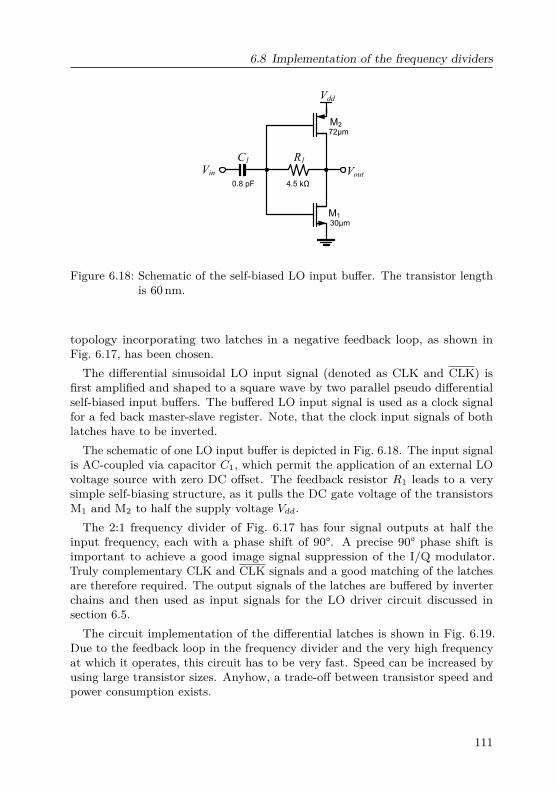
6.8 Implementation of the frequency dividers
Vin Vout
Vdd
0.8 pF
C1 R1
4.5 kΩ
M1
M2
72µm
30µm
Figure 6.18: Schematic of the self-biased LO input buffer. The transistor lengthis 60 nm.
topology incorporating two latches in a negative feedback loop, as shown inFig. 6.17, has been chosen.The differential sinusoidal LO input signal (denoted as CLK and CLK) is
first amplified and shaped to a square wave by two parallel pseudo differentialself-biased input buffers. The buffered LO input signal is used as a clock signalfor a fed back master-slave register. Note, that the clock input signals of bothlatches have to be inverted.
The schematic of one LO input buffer is depicted in Fig. 6.18. The input signalis AC-coupled via capacitor C1, which permit the application of an external LOvoltage source with zero DC offset. The feedback resistor R1 leads to a verysimple self-biasing structure, as it pulls the DC gate voltage of the transistorsM1 and M2 to half the supply voltage Vdd.The 2:1 frequency divider of Fig. 6.17 has four signal outputs at half the
input frequency, each with a phase shift of 90°. A precise 90° phase shift isimportant to achieve a good image signal suppression of the I/Q modulator.Truly complementary CLK and CLK signals and a good matching of the latchesare therefore required. The output signals of the latches are buffered by inverterchains and then used as input signals for the LO driver circuit discussed insection 6.5.The circuit implementation of the differential latches is shown in Fig. 6.19.
Due to the feedback loop in the frequency divider and the very high frequencyat which it operates, this circuit has to be very fast. Speed can be increased byusing large transistor sizes. Anyhow, a trade-off between transistor speed andpower consumption exists.
111
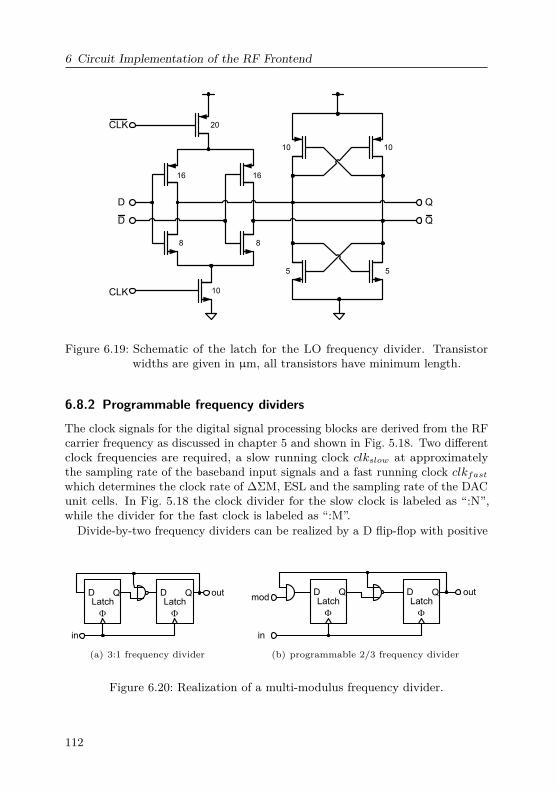
6 Circuit Implementation of the RF Frontend
D
D
CLK
CLK
Q
Q
1010
5 5
16 16
8 8
10
20
Figure 6.19: Schematic of the latch for the LO frequency divider. Transistorwidths are given in µm, all transistors have minimum length.
6.8.2 Programmable frequency dividers
The clock signals for the digital signal processing blocks are derived from the RFcarrier frequency as discussed in chapter 5 and shown in Fig. 5.18. Two differentclock frequencies are required, a slow running clock clkslow at approximatelythe sampling rate of the baseband input signals and a fast running clock clkfastwhich determines the clock rate of ∆ΣM, ESL and the sampling rate of the DACunit cells. In Fig. 5.18 the clock divider for the slow clock is labeled as “:N”,while the divider for the fast clock is labeled as “:M”.
Divide-by-two frequency dividers can be realized by a D flip-flop with positive
LatchD
F
Q out
in
LatchD
F
Q
(a) 3:1 frequency divider
LatchD
F
QLatchD
F
Q out
in
mod
(b) programmable 2/3 frequency divider
Figure 6.20: Realization of a multi-modulus frequency divider.
112
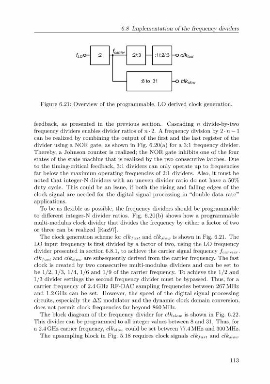
6.8 Implementation of the frequency dividers
:2/:3 :1/:2/:3 clkfastfLO :2
:8 to :31 clkslow
fcarrier
Figure 6.21: Overview of the programmable, LO derived clock generation.
feedback, as presented in the previous section. Cascading n divide-by-twofrequency dividers enables divider ratios of n · 2. A frequency division by 2 ·n− 1can be realized by combining the output of the first and the last register of thedivider using a NOR gate, as shown in Fig. 6.20(a) for a 3:1 frequency divider.Thereby, a Johnson counter is realized; the NOR gate inhibits one of the fourstates of the state machine that is realized by the two consecutive latches. Dueto the timing-critical feedback, 3:1 dividers can only operate up to frequenciesfar below the maximum operating frequencies of 2:1 dividers. Also, it must benoted that integer-N dividers with an uneven divider ratio do not have a 50%duty cycle. This could be an issue, if both the rising and falling edges of theclock signal are needed for the digital signal processing in “double data rate”applications.
To be as flexible as possible, the frequency dividers should be programmableto different integer-N divider ratios. Fig. 6.20(b) shows how a programmablemulti-modulus clock divider that divides the frequency by either a factor of twoor three can be realized [Raz97].
The clock generation scheme for clkfast and clkslow is shown in Fig. 6.21. TheLO input frequency is first divided by a factor of two, using the LO frequencydivider presented in section 6.8.1, to achieve the carrier signal frequency fcarrier.clkfast and clkslow are subsequently derived from the carrier frequency. The fastclock is created by two consecutive multi-modulus dividers and can be set tobe 1/2, 1/3, 1/4, 1/6 and 1/9 of the carrier frequency. To achieve the 1/2 and1/3 divider settings the second frequency divider must be bypassed. Thus, for acarrier frequency of 2.4GHz RF-DAC sampling frequencies between 267MHzand 1.2GHz can be set. However, the speed of the digital signal processingcircuits, especially the ∆Σ modulator and the dynamic clock domain conversion,does not permit clock frequencies far beyond 860MHz.The block diagram of the frequency divider for clkslow is shown in Fig. 6.22.
This divider can be programmed to all integer values between 8 and 31. Thus, fora 2.4GHz carrier frequency, clkslow could be set between 77.4MHz and 300MHz.The upsampling block in Fig. 5.18 requires clock signals clkfast and clkslow
113
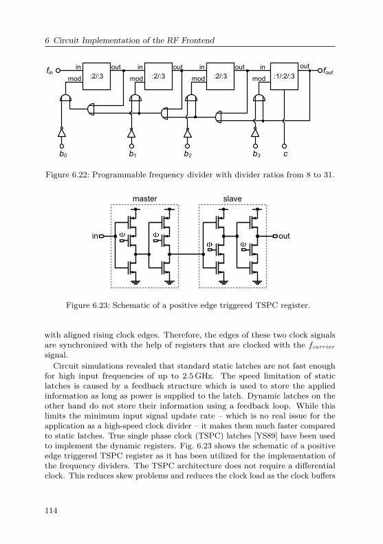
6 Circuit Implementation of the RF Frontend
in out
mod :2/:3
in out
mod :2/:3
in out
mod :2/:3
in out
mod :1/:2/:3foutfin
b0 b1 b2 b3 c
Figure 6.22: Programmable frequency divider with divider ratios from 8 to 31.
master slave
in out
Figure 6.23: Schematic of a positive edge triggered TSPC register.
with aligned rising clock edges. Therefore, the edges of these two clock signalsare synchronized with the help of registers that are clocked with the fcarriersignal.Circuit simulations revealed that standard static latches are not fast enough
for high input frequencies of up to 2.5GHz. The speed limitation of staticlatches is caused by a feedback structure which is used to store the appliedinformation as long as power is supplied to the latch. Dynamic latches on theother hand do not store their information using a feedback loop. While thislimits the minimum input signal update rate – which is no real issue for theapplication as a high-speed clock divider – it makes them much faster comparedto static latches. True single phase clock (TSPC) latches [YS89] have been usedto implement the dynamic registers. Fig. 6.23 shows the schematic of a positiveedge triggered TSPC register as it has been utilized for the implementation ofthe frequency dividers. The TSPC architecture does not require a differentialclock. This reduces skew problems and reduces the clock load as the clock buffers
114
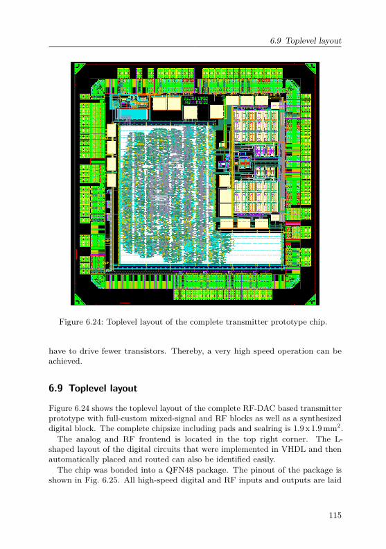
6.9 Toplevel layout
Figure 6.24: Toplevel layout of the complete transmitter prototype chip.
have to drive fewer transistors. Thereby, a very high speed operation can beachieved.
6.9 Toplevel layout
Figure 6.24 shows the toplevel layout of the complete RF-DAC based transmitterprototype with full-custom mixed-signal and RF blocks as well as a synthesizeddigital block. The complete chipsize including pads and sealring is 1.9 x 1.9mm2.The analog and RF frontend is located in the top right corner. The L-
shaped layout of the digital circuits that were implemented in VHDL and thenautomatically placed and routed can also be identified easily.The chip was bonded into a QFN48 package. The pinout of the package is
shown in Fig. 6.25. All high-speed digital and RF inputs and outputs are laid
115
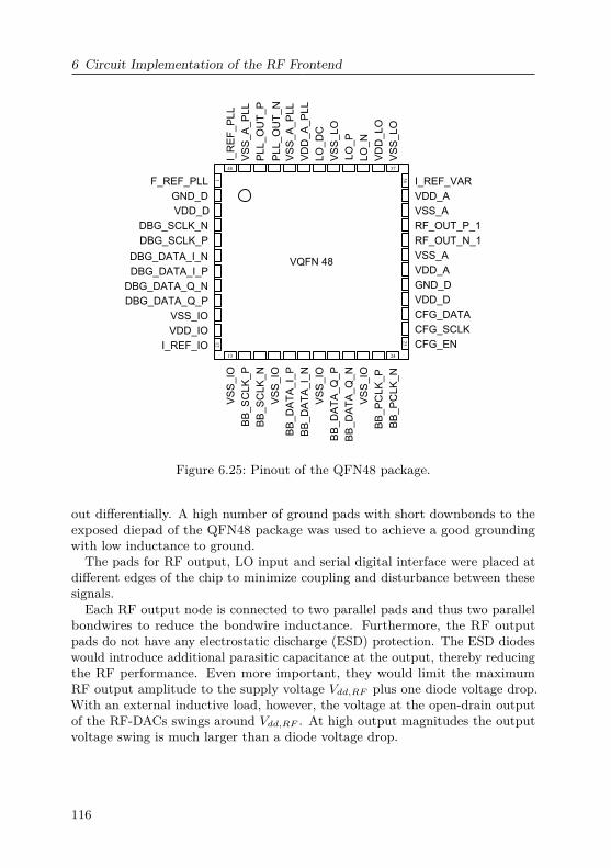
6 Circuit Implementation of the RF Frontend
VQFN 48
112
13 24
36
25
48 37
BB
_P
CL
K_
P
BB
_P
CL
K_
N
VS
S_
IO
BB
_D
AT
A_
I_P
BB
_D
AT
A_
I_N
VS
S_
IO
BB
_D
AT
A_
Q_
P
BB
_D
AT
A_
Q_
N
VS
S_
IO
BB
_S
CL
K_
P
BB
_S
CL
K_
N
GND_D
CFG_EN
CFG_SCLK
CFG_DATA
VSS_A
VDD_A
VSS_A
I_REF_VAR
VS
S_
A_P
LL
LO
_D
C
DBG_DATA_I_N
DBG_DATA_I_P
DBG_DATA_Q_N
DBG_DATA_Q_P
VS
S_
IODBG_SCLK_N
DBG_SCLK_P
PL
L_
OU
T_P
PL
L_
OU
T_N
I_R
EF
_P
LL
F_REF_PLL
RF_OUT_N_1
RF_OUT_P_1
LO
_P
LO
_N
VS
S_
LO
VDD_A
VDD_D
VD
D_L
O
VD
D_A
_P
LL
VDD_D
VSS_IO
VDD_IO
GND_D
I_REF_IOV
SS
_L
O
VS
S_
A_P
LL
Figure 6.25: Pinout of the QFN48 package.
out differentially. A high number of ground pads with short downbonds to theexposed diepad of the QFN48 package was used to achieve a good groundingwith low inductance to ground.
The pads for RF output, LO input and serial digital interface were placed atdifferent edges of the chip to minimize coupling and disturbance between thesesignals.
Each RF output node is connected to two parallel pads and thus two parallelbondwires to reduce the bondwire inductance. Furthermore, the RF outputpads do not have any electrostatic discharge (ESD) protection. The ESD diodeswould introduce additional parasitic capacitance at the output, thereby reducingthe RF performance. Even more important, they would limit the maximumRF output amplitude to the supply voltage Vdd,RF plus one diode voltage drop.With an external inductive load, however, the voltage at the open-drain outputof the RF-DACs swings around Vdd,RF . At high output magnitudes the outputvoltage swing is much larger than a diode voltage drop.
116
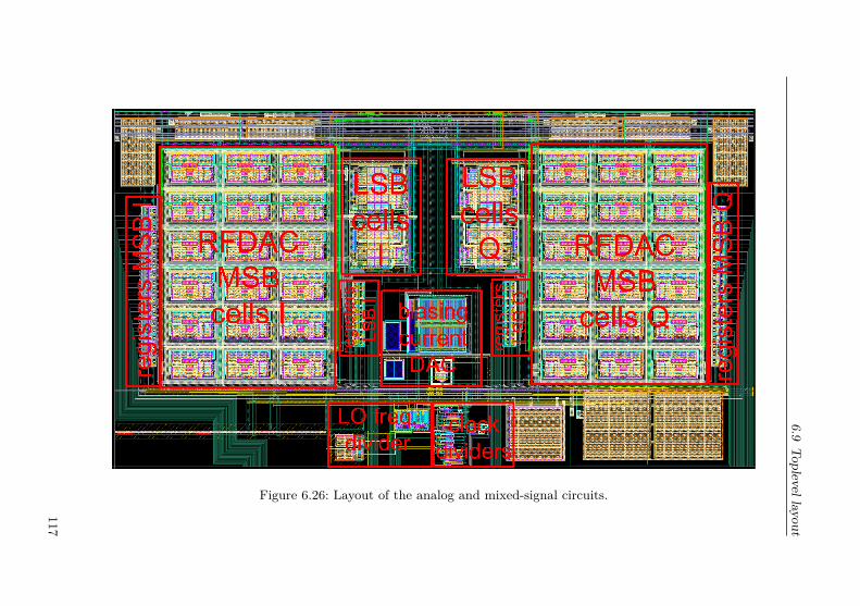
6.9Toplevellayout
Figure 6.26: Layout of the analog and mixed-signal circuits.
117
6 Circuit Implementation of the RF Frontend
As most of the transistors in the transmitter operate as digital switches, peakcurrents that are much higher than the average current can occur. As theswitching frequencies are quite high, such currents lead to a severe voltage dropover the bondwires to ground. Hence, so-called ground bouncing and rippleson the supply lines can occur. Depending on the bondwire inductance, theground bouncing can be up to several hundred millivolts. A good groundingand a stabilization of the supply voltages with on-chip decoupling capacitorsis therefore essential. In the layout plot of Fig. 6.24 the MIM-capacitors thatare used as decoupling capacitors can be identified as large beige rectanglesthat are located around the RF frontend and the digital blocks. The decouplingcapacitors have an overall size of approximately 100 pF.A close-up view of the RF frontend blocks is shown in Fig. 6.26. The active
area of the modulator frontend is approximately 0.4mm2. The inphase andquadrature RF-DAC cells are symmetrically placed around the common biasingblock. Also, the LO frequency divider output is supplied very symmetrically tothe inphase and quadrature RF-DAC cells to achieve a low phase imbalance. Avery dense mesh of ground wires is routed between the RF-DAC unit cells toachieve a low-inductance path to the ground pads.
6.10 Simulation results of the RF-frontend
6.10.1 Simulation setup
All analog and RF blocks have been simulated on transistor level using theCadence Virtuoso Spectre® circuit simulator. For the transistor level simulationsof the RF-frontend, the signal generation and digital processing of the inputsignal have been modeled with the help of Matlab and Verilog-A.Because of the high number of (parallel) building blocks and the high ratio
between baseband signal frequency and RF output frequency, the simulationeffort is tremendous, especially when simulating with modulated input signals.Simulations with complete extracted parasitics are almost impossible, due tothe high complexity.
Even worse, true mixed-signal simulations need two different simulators for thedigital and analog parts. SPICE-like analog simulators have to solve differentialequations, while digital simulators are event driven. The required communicationbetween the parallel running simulators makes this type of simulation very slow.To be able to verify the functionality of the complete chip, mixed-signal toplevelsimulations have been performed with a simple behavioral model of the analogfrontend. This approach is described in section 6.10.3.
118
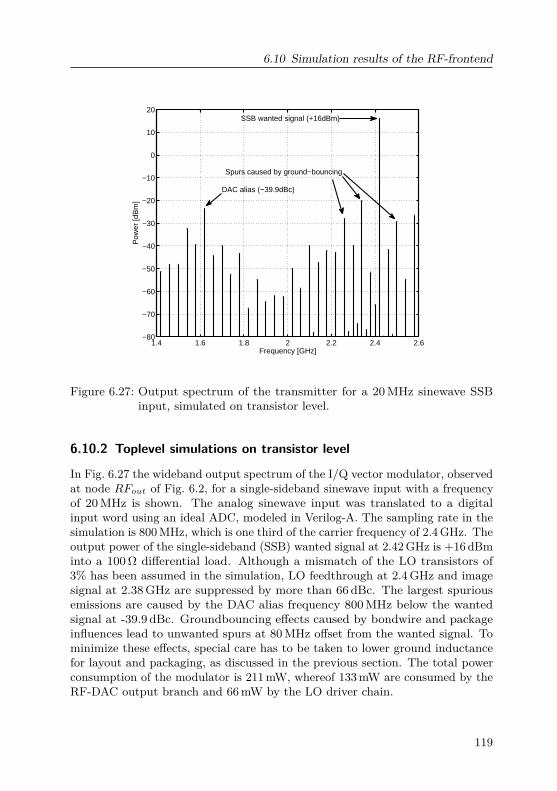
6.10 Simulation results of the RF-frontend
1.4 1.6 1.8 2 2.2 2.4 2.6−80
−70
−60
−50
−40
−30
−20
−10
0
10
20
Frequency [GHz]
Pow
er [d
Bm
]
DAC alias (−39.9dBc)
Spurs caused by ground−bouncing
SSB wanted signal (+16dBm)
Figure 6.27: Output spectrum of the transmitter for a 20MHz sinewave SSBinput, simulated on transistor level.
6.10.2 Toplevel simulations on transistor level
In Fig. 6.27 the wideband output spectrum of the I/Q vector modulator, observedat node RFout of Fig. 6.2, for a single-sideband sinewave input with a frequencyof 20MHz is shown. The analog sinewave input was translated to a digitalinput word using an ideal ADC, modeled in Verilog-A. The sampling rate in thesimulation is 800MHz, which is one third of the carrier frequency of 2.4GHz. Theoutput power of the single-sideband (SSB) wanted signal at 2.42GHz is +16 dBminto a 100Ω differential load. Although a mismatch of the LO transistors of3% has been assumed in the simulation, LO feedthrough at 2.4GHz and imagesignal at 2.38GHz are suppressed by more than 66 dBc. The largest spuriousemissions are caused by the DAC alias frequency 800MHz below the wantedsignal at -39.9 dBc. Groundbouncing effects caused by bondwire and packageinfluences lead to unwanted spurs at 80MHz offset from the wanted signal. Tominimize these effects, special care has to be taken to lower ground inductancefor layout and packaging, as discussed in the previous section. The total powerconsumption of the modulator is 211mW, whereof 133mW are consumed by theRF-DAC output branch and 66mW by the LO driver chain.
119
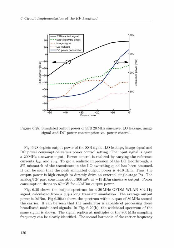
6 Circuit Implementation of the RF Frontend
−50 −40 −30 −20 −10 0−80
−70
−60
−50
−40
−30
−20
−10
0
10
20
Power control
Out
put p
ower
[dB
m]
−50 −40 −30 −20 −10 00
100
200
300
400
Con
sum
ed p
ower
[mW
]
SSB wanted signalspur @80MHz offsetimage signalLO leakageDC power consumtion
Figure 6.28: Simulated output power of SSB 20MHz sinewave, LO leakage, imagesignal and DC power consumption vs. power control.
Fig. 6.28 depicts output power of the SSB signal, LO leakage, image signal andDC power consumption versus power control setting. The input signal is againa 20MHz sinewave input. Power control is realized by varying the referencecurrents Iin1 and Iin2. To get a realistic impression of the LO feedthrough, a3% mismatch of the transistors in the LO switching quad has been assumed.It can be seen that the peak simulated output power is +19 dBm. Thus, theoutput power is high enough to directly drive an external single-stage PA. Theanalog/RF part consumes about 300mW at +19 dBm sinewave output. Powerconsumption drops to 67mW for -30 dBm output power.Fig. 6.29 shows the output spectrum for a 20MHz OFDM WLAN 802.11g
signal, calculated from a 50µs long transient simulation. The average outputpower is 0 dBm. Fig 6.29(a) shows the spectrum within a span of 80MHz aroundthe carrier. It can be seen that the modulator is capable of processing thesebroadband modulated signals. In Fig. 6.29(b), the wideband spectrum of thesame signal is shown. The signal replica at multiples of the 800MHz samplingfrequency can be clearly identified. The second harmonic of the carrier frequency
120
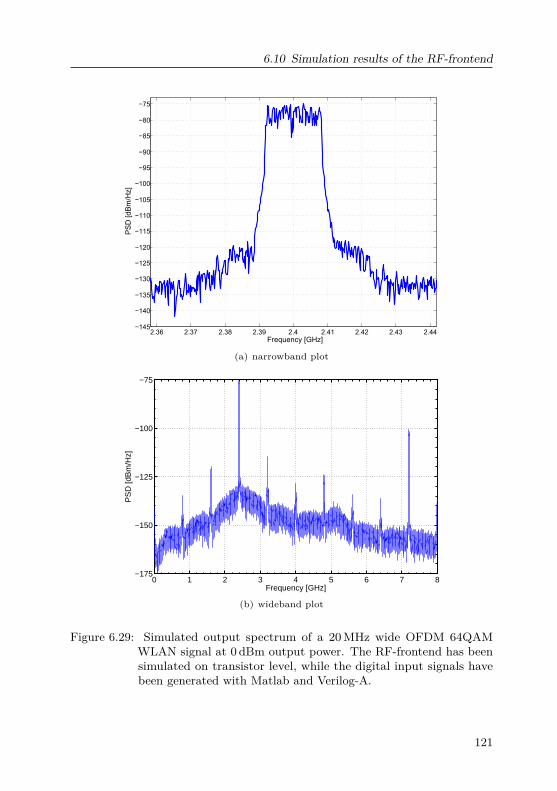
6.10 Simulation results of the RF-frontend
2.36 2.37 2.38 2.39 2.4 2.41 2.42 2.43 2.44−145
−140
−135
−130
−125
−120
−115
−110
−105
−100
−95
−90
−85
−80
−75
Frequency [GHz]
PS
D [d
Bm
/Hz]
(a) narrowband plot
0 1 2 3 4 5 6 7 8−175
−150
−125
−100
−75
Frequency [GHz]
PS
D [
dB
m/H
z]
(b) wideband plot
Figure 6.29: Simulated output spectrum of a 20MHz wide OFDM 64QAMWLAN signal at 0 dBm output power. The RF-frontend has beensimulated on transistor level, while the digital input signals havebeen generated with Matlab and Verilog-A.
121
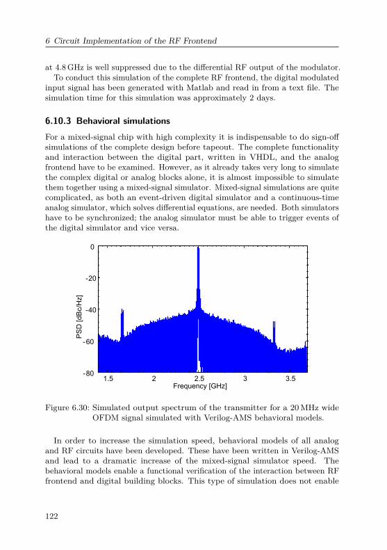
6 Circuit Implementation of the RF Frontend
at 4.8GHz is well suppressed due to the differential RF output of the modulator.To conduct this simulation of the complete RF frontend, the digital modulated
input signal has been generated with Matlab and read in from a text file. Thesimulation time for this simulation was approximately 2 days.
6.10.3 Behavioral simulationsFor a mixed-signal chip with high complexity it is indispensable to do sign-offsimulations of the complete design before tapeout. The complete functionalityand interaction between the digital part, written in VHDL, and the analogfrontend have to be examined. However, as it already takes very long to simulatethe complex digital or analog blocks alone, it is almost impossible to simulatethem together using a mixed-signal simulator. Mixed-signal simulations are quitecomplicated, as both an event-driven digital simulator and a continuous-timeanalog simulator, which solves differential equations, are needed. Both simulatorshave to be synchronized; the analog simulator must be able to trigger events ofthe digital simulator and vice versa.
1.5 2 2.5 3 3.5-80
-60
-40
-20
0
Frequency [GHz]
PS
D [d
Bc/H
z]
Figure 6.30: Simulated output spectrum of the transmitter for a 20MHz wideOFDM signal simulated with Verilog-AMS behavioral models.
In order to increase the simulation speed, behavioral models of all analogand RF circuits have been developed. These have been written in Verilog-AMSand lead to a dramatic increase of the mixed-signal simulator speed. Thebehavioral models enable a functional verification of the interaction between RFfrontend and digital building blocks. This type of simulation does not enable
122

6.10 Simulation results of the RF-frontend
real performance measurements. However, it allows to investigate the effects ofdifferent settings for the digital signal processing on the RF output spectrum.One simulation run of the real valued behavioral model with a mixed-signalsimulator takes only three hours. It is estimated that one simulation run of thecomplete chip with the analog frontend modeled on transistor level would requireapproximately 1360 hours (57 days) to finish. The simulated output spectrum ofa behavioral simulation of the complete transmitter for a 20MHz OFDM signalwith a sampling rate of 833MHz is shown in Fig. 6.30.
Furthermore, a high-level abstraction of the complete RF-frontend using theVerilog-AMS “wreal” datatype as a real-valued model has been developed. The“wreal” datatype permits the utilization of 32 bit floating point numbers for theevent-driven simulation. Thereby, the “wreal” datatype has the same amplituderesolution as analog simulations, however, because of the event-driven modeling,they are only calculated at discrete points in time [Joe08]. This enables evenfaster functional verifications that require the digital simulator only.
123

124
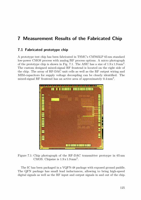
7 Measurement Results of the Fabricated Chip
7.1 Fabricated prototype chip
A prototype test chip has been fabricated in TSMC’s CMN65LP 65 nm standardlow-power CMOS process with analog/RF process options. A micro photographof the prototype chip is shown in Fig. 7.1. The ASIC has a size of 1.9 x 1.9mm2.The custom designed mixed-signal RF frontend is located on the right side ofthe chip. The array of RF-DAC unit cells as well as the RF output wiring andMIM-capacitors for supply voltage decoupling can be clearly identified. Themixed-signal RF frontend has an active area of approximately 0.4mm2.
Figure 7.1: Chip photograph of the RF-DAC transmitter protoype in 65 nmCMOS. Chipsize is 1.9 x 1.9mm2.
The IC has been packaged in a VQFN-48 package with exposed ground paddle.The QFN package has small lead inductances, allowing to bring high-speeddigital signals as well as the RF input and output signals in and out of the chip.
125
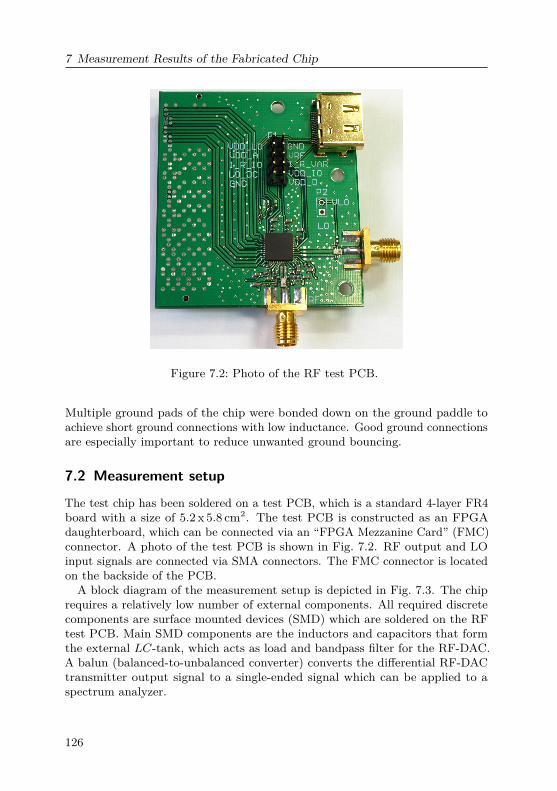
7 Measurement Results of the Fabricated Chip
Figure 7.2: Photo of the RF test PCB.
Multiple ground pads of the chip were bonded down on the ground paddle toachieve short ground connections with low inductance. Good ground connectionsare especially important to reduce unwanted ground bouncing.
7.2 Measurement setup
The test chip has been soldered on a test PCB, which is a standard 4-layer FR4board with a size of 5.2 x 5.8 cm2. The test PCB is constructed as an FPGAdaughterboard, which can be connected via an “FPGA Mezzanine Card” (FMC)connector. A photo of the test PCB is shown in Fig. 7.2. RF output and LOinput signals are connected via SMA connectors. The FMC connector is locatedon the backside of the PCB.A block diagram of the measurement setup is depicted in Fig. 7.3. The chip
requires a relatively low number of external components. All required discretecomponents are surface mounted devices (SMD) which are soldered on the RFtest PCB. Main SMD components are the inductors and capacitors that formthe external LC-tank, which acts as load and bandpass filter for the RF-DAC.A balun (balanced-to-unbalanced converter) converts the differential RF-DACtransmitter output signal to a single-ended signal which can be applied to aspectrum analyzer.
126
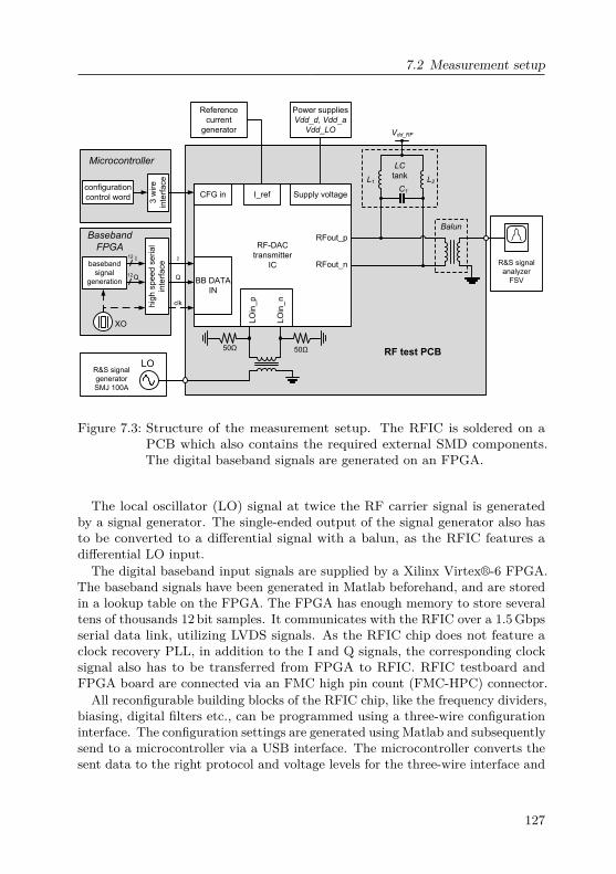
7.2 Measurement setup
LC
tank
Vdd_RF
LO
baseband
signal
generation
hig
h s
pe
ed
se
ria
l
inte
rfa
ce
Q
I
XO
Q
I
clk
12
12
Baseband
FPGA
3 w
ire
inte
rfa
ce
configuration
control word
Microcontroller
RF-DAC
transmitter
IC
CFG in
BB DATA
IN
RFout_p
RFout_n
L1 L2
C1
Balun
50Ω50Ω
LO
in_p
LO
in_n
R&S signal
generator
SMJ 100A
R&S signal
analyzer
FSV
I_ref Supply voltage
Power supplies
Vdd_d, Vdd_a
Vdd_LO
Reference
current
generator
RF test PCB
Figure 7.3: Structure of the measurement setup. The RFIC is soldered on aPCB which also contains the required external SMD components.The digital baseband signals are generated on an FPGA.
The local oscillator (LO) signal at twice the RF carrier signal is generatedby a signal generator. The single-ended output of the signal generator also hasto be converted to a differential signal with a balun, as the RFIC features adifferential LO input.
The digital baseband input signals are supplied by a Xilinx Virtex®-6 FPGA.The baseband signals have been generated in Matlab beforehand, and are storedin a lookup table on the FPGA. The FPGA has enough memory to store severaltens of thousands 12 bit samples. It communicates with the RFIC over a 1.5Gbpsserial data link, utilizing LVDS signals. As the RFIC chip does not feature aclock recovery PLL, in addition to the I and Q signals, the corresponding clocksignal also has to be transferred from FPGA to RFIC. RFIC testboard andFPGA board are connected via an FMC high pin count (FMC-HPC) connector.
All reconfigurable building blocks of the RFIC chip, like the frequency dividers,biasing, digital filters etc., can be programmed using a three-wire configurationinterface. The configuration settings are generated using Matlab and subsequentlysend to a microcontroller via a USB interface. The microcontroller converts thesent data to the right protocol and voltage levels for the three-wire interface and
127
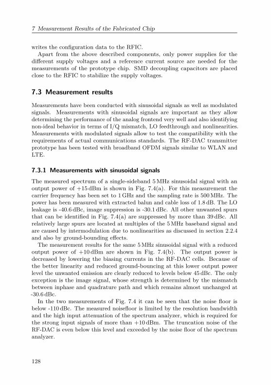
7 Measurement Results of the Fabricated Chip
writes the configuration data to the RFIC.Apart from the above described components, only power supplies for the
different supply voltages and a reference current source are needed for themeasurements of the prototype chip. SMD decoupling capacitors are placedclose to the RFIC to stabilize the supply voltages.
7.3 Measurement results
Measurements have been conducted with sinusoidal signals as well as modulatedsignals. Measurements with sinusoidal signals are important as they allowdetermining the performance of the analog frontend very well and also identifyingnon-ideal behavior in terms of I/Q mismatch, LO feedthrough and nonlinearities.Measurements with modulated signals allow to test the compatibility with therequirements of actual communications standards. The RF-DAC transmitterprototype has been tested with broadband OFDM signals similar to WLAN andLTE.
7.3.1 Measurements with sinusoidal signalsThe measured spectrum of a single-sideband 5MHz sinusoidal signal with anoutput power of +15 dBm is shown in Fig. 7.4(a). For this measurement thecarrier frequency has been set to 1GHz and the sampling rate is 500MHz. Thepower has been measured with extracted balun and cable loss of 1.8 dB. The LOleakage is -40.6 dBc, image suppression is -30.1 dBc. All other unwanted spursthat can be identified in Fig. 7.4(a) are suppressed by more than 39 dBc. Allrelatively large spurs are located at multiples of the 5MHz baseband signal andare caused by intermodulation due to nonlinearities as discussed in section 2.2.4and also by ground-bounding effects.
The measurement results for the same 5MHz sinusoidal signal with a reducedoutput power of +10 dBm are shown in Fig. 7.4(b). The output power isdecreased by lowering the biasing currents in the RF-DAC cells. Because ofthe better linearity and reduced ground-bouncing at this lower output powerlevel the unwanted emission are clearly reduced to levels below 45 dBc. The onlyexception is the image signal, whose strength is determined by the mismatchbetween inphase and quadrature path and which remains almost unchanged at-30.6 dBc.
In the two measurements of Fig. 7.4 it can be seen that the noise floor isbelow -110 dBc. The measured noisefloor is limited by the resolution bandwidthand the high input attenuation of the spectrum analyzer, which is required forthe strong input signals of more than +10dBm. The truncation noise of theRF-DAC is even below this level and exceeded by the noise floor of the spectrumanalyzer.
128
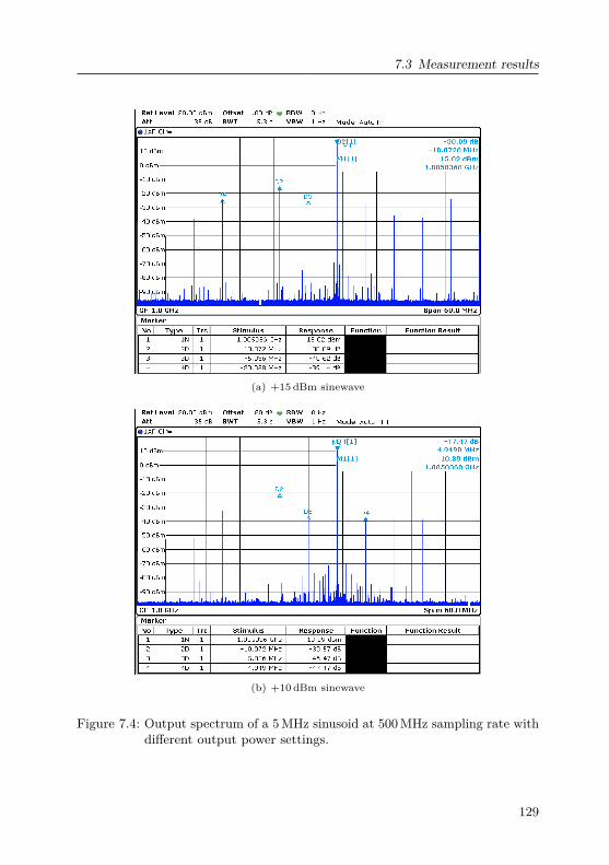
7.3 Measurement results
(a) +15 dBm sinewave
(b) +10 dBm sinewave
Figure 7.4: Output spectrum of a 5MHz sinusoid at 500MHz sampling rate withdifferent output power settings.
129
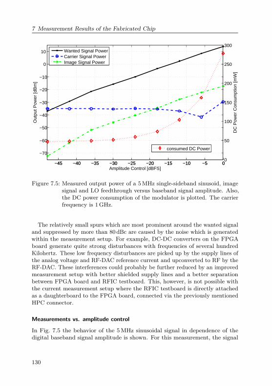
7 Measurement Results of the Fabricated Chip
−45 −40 −35 −30 −25 −20 −15 −10 −5 0
−70
−60
−50
−40
−30
−20
−10
0
10
Amplitude Control [dBFS]
Out
put P
ower
[dB
m]
−45 −40 −35 −30 −25 −20 −15 −10 −5 00
50
100
150
200
250
300
DC
Pow
er C
onsu
mpt
ion
[mW
]
Wanted Signal PowerCarrier Signal PowerImage Signal Power
consumed DC Power
Figure 7.5: Measured output power of a 5MHz single-sideband sinusoid, imagesignal and LO feedthrough versus baseband signal amplitude. Also,the DC power consumption of the modulator is plotted. The carrierfrequency is 1GHz.
The relatively small spurs which are most prominent around the wanted signaland suppressed by more than 80 dBc are caused by the noise which is generatedwithin the measurement setup. For example, DC-DC converters on the FPGAboard generate quite strong disturbances with frequencies of several hundredKilohertz. These low frequency disturbances are picked up by the supply lines ofthe analog voltage and RF-DAC reference current and upconverted to RF by theRF-DAC. These interferences could probably be further reduced by an improvedmeasurement setup with better shielded supply lines and a better separationbetween FPGA board and RFIC testboard. This, however, is not possible withthe current measurement setup where the RFIC testboard is directly attachedas a daughterboard to the FPGA board, connected via the previously mentionedHPC connector.
Measurements vs. amplitude control
In Fig. 7.5 the behavior of the 5MHz sinusoidal signal in dependence of thedigital baseband signal amplitude is shown. For this measurement, the signal
130
7.3 Measurement results
Power consumption [mW]Digitally contr. LO driver LO driver always on0 dBFS -48 dBFS 0 dBFS -48 dBFS
RF-DAC outputbranch
214.3 0.8 214.6 0.8
Biasing 23 23.3 23 23.3LO driver chain 41.3 22.3 57.3 56.4total 278.6 46.4 294.9 80.5
Table 7.1: Power consumption of the analog and RF blocks at different digitalbaseband signal magnitudes for a fixed biasing and +13.8 dBm outputpower with full scale amplitude.
amplitude is scaled by shifting the digital word by one bit towards the LSBfor each amplitude control step. With each step the digital baseband signalamplitude is reduced by a factor of two. The wanted signal output power scalesvery linearly by 6 dB per amplitude control step over a dynamic range of 48 dB,as expected for an amplitude resolution of 8 bit. The biasing conditions havebeen set to a peak output power of 13.8 dBm for a full-scale sinusoidal signal.The image signal scales correspondingly to the wanted signal and is suppressedby approximately 30 dBc over the complete amplitude control range. The LOleakage remains relatively constant at a power of approximately -35 dBm. Itis increased to -22 dBm (not shown in Fig. 7.5) if the LO drivers of inactiveRF-DAC unit cells are configured to be constantly in “on” state, instead of beingcontrolled by the output magnitude, as described in section 6.5.
The DC power consumption of the modulator drops from 278mW for a fullscale sinusoidal output to 46mW at -48 dBFS, which shows the effectivenessof the power saving mechanisms for low signal magnitudes, namely completelyturning of the current-flow in inactive RF-DAC cells as well as deactivatingthe corresponding LO driver cells. The power consumption of the differentmodulator building blocks – RF-DAC output branch, biasing circuits, and LOdriver chain including the 2:1 frequency divider – for different amplitudes anddifferent LO driver control settings is summarized in table 7.1. As can beseen, the RF-DAC output branch dominates the total power consumption forlarge signal amplitudes, while biasing and LO driver chain dominate for smallamplitudes.
131
7 Measurement Results of the Fabricated Chip
Power consumption [mW]Pout=+16dBm Pout=0dBm Pout=-20 dBm
RF-DAC outputbranch
358 42 3.7
Biasing 29.9 5 2.1LO driver chain 29.2 29.5 29.4total 403.7 76.5 35.2
Table 7.2: Power consumption of the analog and RF blocks at different outputpower settings for a full-scale sinusoidal signal. The power control isdone by scaling the bias currents of the RF-DAC unit cells.
Power control measurements
Besides reducing the digital baseband signal magnitude, the output power ofthe RF-DAC transmitter can also be controlled by changing the bias currents inthe RF-DAC unit cells, without having to sacrifice converter resolution. Theimplementation of the RF-DAC bias control has been described in section 6.7.The power control of the transmitter is not fast enough to do amplitude modula-tion. Rather, it is typically used to set the average output power level, e.g. independence of the distance and channel quality between handheld device andbasestation.
In Fig. 7.6 the output power of the RF-DAC versus power control is shown fora 5MHz single-sideband, full-scale sinusoidal signal at 1GHz carrier frequency.Also, the image signal and LO feedthrough, as well as the power consumption ofthe modulator are shown. In Fig. 7.6(a) the signal power is measured while theLO driver is dynamically controlled by the digital signal magnitude, in Fig. 7.6(b)all LO driver cells are constantly running.The peak output power which could be measured with a sinusoidal signal is
more than +16 dBm, which is the highest reported output power for an RF-DACbased modulator. It is about 14 dB more than reported in [Elo+07] and 24 dBmore than in [JS07]. At the same time, the active area of the analog blocks isonly 0.4mm2 and thus distinctively smaller than the values reported in [Elo+07]and [JS07].The power control has a dynamic range of almost 90 dB; the wanted signal
power can be decreased down to -70 dBm. The image signal power scales withthe wanted signal power until it reaches -80 dBm. The minimum LO feedthroughlevels that can be achieved are -32 dBm if the LO is dynamically controlled, or-24 dBm if it is constantly running.
132
7.3 Measurement results
−80 −70 −60 −50 −40 −30 −20 −10 0
−80
−70
−60
−50
−40
−30
−20
−10
0
10
20
Power Control [dB]
Out
put P
ower
[dB
m]
−80 −70 −60 −50 −40 −30 −20 −10 00
50
100
150
200
250
300
350
400
450
500
DC
Pow
er C
onsu
mpt
ion
[mW
]
Wanted Signal PowerCarrier Signal PowerImage Signal Power
consumed DC Power
(a) with amplitude controlled LO buffer
−80 −70 −60 −50 −40 −30 −20 −10 0
−80
−70
−60
−50
−40
−30
−20
−10
0
10
20
Power Control [dB]
Out
put P
ower
[dB
m]
−80 −70 −60 −50 −40 −30 −20 −10 00
50
100
150
200
250
300
350
400
450
500
DC
Pow
er C
onsu
mpt
ion
[mW
]
Wanted Signal PowerCarrier Signal PowerImage Signal Power
consumed DC Power
(b) LO constantly running
Figure 7.6: Measured output power of a 5MHz single-sideband sinusoid (full-scale), image signal and LO feedthrough versus power control. Also,the DC power consumption of the modulator is plotted. The carrierfrequency is 1GHz.
133
7 Measurement Results of the Fabricated Chip
In table 7.2 the measured power consumption of the different modulator blocksis given for different output power levels. The total power consumption dropsfrom approximately 400mW at the peak RF output power of +16 dBm to 35mWat -20 dBm output power. In difference to the case of Fig. 7.5 and table 7.1, wherethe digital signal magnitude is scaled, here the LO driver power consumptionstays constant, while the power in the biasing blocks scales with power control.The overall power efficiency of the modulator at +16 dBm output power is morethan 10%.If all LO drivers are continuously running it limits the minimum modulator
power consumption to 42mW. By switching off the LO driver of inactive RF-DACunit cells, the power consumption can be reduced by 15mW.
Issues detected during the measurements
The LO input 2:1 frequency diver can be operated up to input frequencies ofapproximately 5GHz and respective output frequencies up to 2.5GHz whichis slightly lower than the maximum simulated output frequency of 2.7GHz.This degradation is caused by underestimated parasitic capacitances at theLO driver output network which increase the load of the frequency divider.Unfortunately, the LO frequency divider also does not work as expected forinput frequencies between approximately 2.8GHz and 3.6GHz. Measurementsreveal that the frequency divider either oscillates or divides by a factor of fourinstead of the wanted factor of two in this input frequency range. This behavioris probably caused by disturbances due to ground-bouncing and an imperfect,slightly unsymmetrical load at the output of the differential frequency divider.Improved ground wiring, a more symmetrical load, additional buffer stages andbetter decoupling of the power supplies should solve this problem. However, itis difficult to reproduce this unwanted behavior in the circuit simulations.
Because of issues in the implementation of the dynamic clock domain conversion(CDC) block, one of the quadrature I/Q paths does not work properly aboveRF carrier frequencies of 1.8GHz. Thus, only double-sideband sinusoidal signalscan be transmitted at these frequencies, making a comprehensive analysis of theRF frontend performance at these high frequencies impossible. A modified CDCimplementation should fix this issue for future implementations.Furthermore, a perturbation of the digital blocks for high modulator output
power levels and high RF carrier frequencies can be observed. These are causedby ground-bouncing and substrate noise. An even better shielding by puttingsensitive circuits into deep n-wells and reducing the ground-bouncing by evenmore bondwires, wider and possibly shorter ground wires on the chip, and betterdecoupling of the supply voltages should reduce this issue.
134
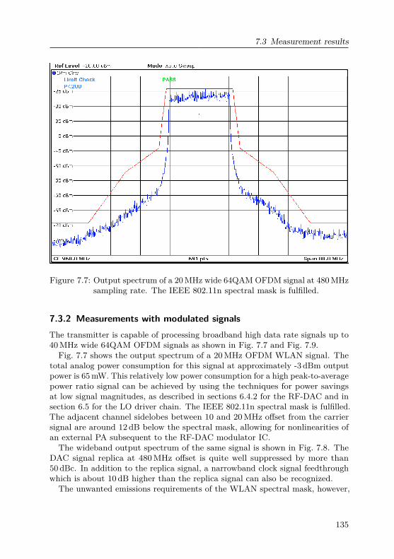
7.3 Measurement results
Figure 7.7: Output spectrum of a 20MHz wide 64QAM OFDM signal at 480MHzsampling rate. The IEEE 802.11n spectral mask is fulfilled.
7.3.2 Measurements with modulated signalsThe transmitter is capable of processing broadband high data rate signals up to40MHz wide 64QAM OFDM signals as shown in Fig. 7.7 and Fig. 7.9.
Fig. 7.7 shows the output spectrum of a 20MHz OFDM WLAN signal. Thetotal analog power consumption for this signal at approximately -3 dBm outputpower is 65mW. This relatively low power consumption for a high peak-to-averagepower ratio signal can be achieved by using the techniques for power savingsat low signal magnitudes, as described in sections 6.4.2 for the RF-DAC and insection 6.5 for the LO driver chain. The IEEE 802.11n spectral mask is fulfilled.The adjacent channel sidelobes between 10 and 20MHz offset from the carriersignal are around 12 dB below the spectral mask, allowing for nonlinearities ofan external PA subsequent to the RF-DAC modulator IC.The wideband output spectrum of the same signal is shown in Fig. 7.8. The
DAC signal replica at 480MHz offset is quite well suppressed by more than50 dBc. In addition to the replica signal, a narrowband clock signal feedthroughwhich is about 10 dB higher than the replica signal can also be recognized.
The unwanted emissions requirements of the WLAN spectral mask, however,
135
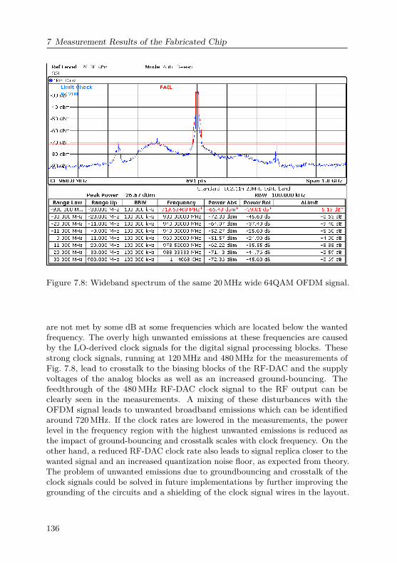
7 Measurement Results of the Fabricated Chip
Figure 7.8: Wideband spectrum of the same 20MHz wide 64QAM OFDM signal.
are not met by some dB at some frequencies which are located below the wantedfrequency. The overly high unwanted emissions at these frequencies are causedby the LO-derived clock signals for the digital signal processing blocks. Thesestrong clock signals, running at 120MHz and 480MHz for the measurements ofFig. 7.8, lead to crosstalk to the biasing blocks of the RF-DAC and the supplyvoltages of the analog blocks as well as an increased ground-bouncing. Thefeedthrough of the 480MHz RF-DAC clock signal to the RF output can beclearly seen in the measurements. A mixing of these disturbances with theOFDM signal leads to unwanted broadband emissions which can be identifiedaround 720MHz. If the clock rates are lowered in the measurements, the powerlevel in the frequency region with the highest unwanted emissions is reduced asthe impact of ground-bouncing and crosstalk scales with clock frequency. On theother hand, a reduced RF-DAC clock rate also leads to signal replica closer to thewanted signal and an increased quantization noise floor, as expected from theory.The problem of unwanted emissions due to groundbouncing and crosstalk of theclock signals could be solved in future implementations by further improving thegrounding of the circuits and a shielding of the clock signal wires in the layout.
136
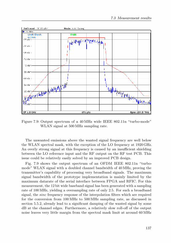
7.3 Measurement results
Figure 7.9: Output spectrum of a 40MHz wide IEEE 802.11n “turbo-mode”WLAN signal at 500MHz sampling rate.
The unwanted emissions above the wanted signal frequency are well belowthe WLAN spectral mask, with the exception of the LO frequency at 1920GHz.An overly strong signal at this frequency is caused by an insufficient shieldingbetween the LO reference input and the RF output on the RF test PCB. Thisissue could be relatively easily solved by an improved PCB design.Fig. 7.9 shows the output spectrum of an OFDM IEEE 802.11n “turbo-
mode” WLAN signal with a doubled channel bandwidth of 40MHz, proving thetransmitter’s capability of processing very broadband signals. The maximumsignal bandwidth of the prototype implementation is mainly limited by themaximum datarate of the serial interface between FPGA and RFIC. For thismeasurement, the 12 bit wide baseband signal has been generated with a samplingrate of 100MHz, yielding a oversampling rate of only 2.5. For such a broadbandsignal, the sinc frequency response of the interpolation filters which are requiredfor the conversion from 100MHz to 500MHz sampling rate, as discussed insection 5.5.2, already lead to a significant damping of the wanted signal by somedB at the channel edges. Furthermore, a relatively slow roll-off of the outputnoise leaves very little margin from the spectral mask limit at around 60MHz
137

7 Measurement Results of the Fabricated Chip
below the carrier frequency.The spectral shape of the measured signals indicates a good signal quality.
However, EVM measurements of OFDM modulated signals could unfortunatelynot be conducted with the existing measurement setup. Enhanced signal genera-tion and signal measurement equipment is required for this task. ConductingEVM measurements hence remains part of future investigations.
138
8 Conclusions and Outlook
8.1 Conclusions
In this thesis a “direct-digital” transmitter for wireless communications, basedon an RF-DAC has been presented. The RF-DAC unites D/A converter andupconversion mixer functionality in a monolithic building block which featuresa digital baseband input and an analog RF output. Thereby, the RF-DACbased transmitter allows to eliminate all analog baseband blocks like filtersor VGAs. As digital signal processing blocks can be much easier reconfiguredfor different requirements compared to analog circuits, this approach enablesthe implementation of a transmitter which supports different communicationstandards, different modes (e.g. signal bandwidths) and operation in differentfrequency bands. It therefore is a step towards a software defined radio.The implemented transmitter shall support broadband, high-data-rate com-
munication standards such as WLAN and 3GPP LTE. These modern standardsare based on OFDM. The modulated signals are distributed on several parallelsubcarriers which are equally spaced around a common RF carrier signal, therebycreating one broadband signal. This technique, in connection with high ordermodulation schemes, leads to very high data rates as well as good bandwidthefficiencies. However, as discussed in chapter 2, OFDM poses exacting demandson the performance of the RF transmitter frontend as high linearity is neededand very large peak to average power ratios (PAPR) of more than 10 dB have tobe supported.
The transmitter frontend of a communications device for consumer applicationsshould be as highly integrated into a monolithic chip as possible to gain lowproduction costs and low required area in a mobile device. Today’s transmitterimplementations typically feature an external power amplifier (PA) which isimplemented in a specialized GaAs or SiGe technology to obtain the high requiredoutput power and linearity. Within the framework of this thesis it has beeninvestigated what output power levels can be realized with a singe-chip nanoscaleCMOS PA solution. Therefore, two PAs with different architectures have beenimplemented in a 130 nm standard CMOS technology. The implementationdetails are presented in chapter 3. It is found that saturated peak outputpowers of more than 27 dBm can be achieved. These power levels are sufficientfor connectivity standards with either relatively low output power levels likeBluetooth or WLAN or with low requirements on the RF frontend linearity, like
139
8 Conclusions and Outlook
DECT. Nonetheless, it is concluded from the obtained results as well as fromliterature that it is not possible to achieve the requirements of cellular standardssuch as UMTS or LTE that demand high linear output power levels in the orderof +33 dBm with a PA which is integrated into the transceiver IC in today’sstandard CMOS technology.Hence, for a transmitter which is intended to support cellular standards an
architecture with a fully integrated modulator plus an external PA has to bechosen. An RF-DAC based topology seems to be an excellent architecturefor broadband, reconfigurable transmitters in nanoscale CMOS. Several earlierpublished digital-RF architectures, which are akin to the RF-DAC approach, arereviewed in chapter 4. As the RF-DAC unites D/A converter and upconversionmixer in a single building block and eliminates all analog baseband signalprocessing it is not possible to implement an analog reconstruction filter at theDAC output. Therefore, unwanted DAC output signal replicas at multiples ofthe DAC sampling rate are upconverted to RF and emitted by the antenna.These unwanted emissions must be very small in order to not disturb parallelrunning radios operating at the respective frequencies. Various techniques suchas a high DAC oversampling ratio, high DAC resolution, and ∆Σ noise shapingin connection with bandpass-filtering at the RF output may help to reduce theunwanted emissions. In addition, the zero-order hold behavior of the DAC has asinc frequency response which creates notches at multiples of the sampling rate,thereby helping to suppress DAC signal replicas.A transmitter architecture has to be found which may achieve the perfor-
mance that is required by the different supported communication standardsand frequency bands and takes into account the special characteristics of theRF-DAC. Maximum spurious emission limits have been calculated and a Matlabsystem simulation has been set up to evaluate the influence of architecturalchoices and the behavior of different building blocks on the overall transmitterperformance. In chapter 5 it is found that a polar modulator architecture doesnot provide enough bandwidth for very broadband signal transmission. Instead,a quadrature I/Q modulator is needed. The RF-DAC modulator must have aresolution of 9 bit for each quadrature path to attain the system requirements.Preceding the RF-DAC the digital input signal has to be oversampled up to800MHz. A ∆Σ modulator allows to do noise shaping to improve SNR in thesignal band. Moreover, additional notches in the noise transfer function of the∆Σ modulator reduce the noise at especially critical frequency bands, such as theduplex frequency band in FDD systems. An element selection logic allows to domismatch shaping and thereby reduces the transmitter performance degradationcaused by analog non-idealities.
The circuit implementation of the mixed-signal and RF frontend is discussedin chapter 6. Particularly, a novel RF-DAC implementation is presented. TheRF-DAC consists of several parallel unit cells. It is implemented as a segmented
140
8.1 Conclusions
architecture with four binary weighted LSBs and four unary weighted MSBs.Thereby, low glitches can be obtained while remaining a relatively low wiringcomplexity. The sign of the output signal can be set by a differential transistorpair which steers the output current either to the positive or negative DACoutput. The presented RF-DAC architecture is optimized for especially highoutput power levels up to +16 dBm. This is achieved by a circuit architecturewhich requires very low voltage headroom and thus leads to a high outputvoltage swing. Furthermore, when operated at small signal amplitudes this novelarchitecture consumes less current than previously published implementations,as unit cells which are inactive can be completely switched off. Also, the LOdriver chain which amounts perceptible to the total power consumption of the RFfrontend is optimized for reduced current consumption at small signal amplitudes.This can be achieved as every RF-DAC MSB unit cell has its own LO driver. Ifa unit cell is inactive, also the corresponding LO driver can be deactivated.
The RF-DAC transmitter has been implemented in a 65 nm standard CMOStechnology. The size of the prototype chip is 1.9x1.9mm2. The analog andmixed-signal parts have an active area of approximately 0.4mm2.
Measurements of the prototype chip reveal that a peak output power up to+16 dBm for a single-sideband sinusoidal signal is possible with the implementedRF-DAC based transmitter. This is the highest reported output power fora direct-digital transmitter. The LO carrier leakage is less than -40 dBc, theimage signal is suppressed by more than 30 dBc. The power consumption of themodulator for the +16 dBm sinusoidal signal is 400mW.
The amplitude of the RF-DAC output can be varied linearly over the completedynamic range of 48 dB, as expected for 8 bit amplitude resolution. Due tothe previously described power saving techniques of RF-DAC and LO driverat low output amplitudes, the power consumption decreases by a factor of sixfor -48 dBFS amplitudes. In addition to the amplitude control, the outputpower can be controlled via the biasing current of the RF-DAC over a dynamicrange of almost 90 dB. However, at very low output signal power levels, the LOfeedthrough is larger than the wanted signal.
The RF-DAC transmitter is capable of processing 64QAM-modulated high-data-rate OFDM signals up to 40MHz channel bandwidth and fulfills the WLANIEEE 802.11n spectral mask around the carrier. Due to the high resolution andsampling rate of the transmitter, spurious emissions at multiples of the DACsampling rate are well suppressed in the measurements. The first signal DACsignal replica for a sampling rate of 500MHz is suppressed by more than 50 dBc.However, due to high ground-bouncing and clock-feedthrough, unexpectedlyhigh spurious emissions at multiples of the clock signals of the digital circuitscan be identified in the output spectrum.
141
8 Conclusions and Outlook
8.2 Outlook
A further improved layout could help to decrease ground-bouncing and clock-feedthrough to the RF-output and biasing circuits. Also, the LO feedthroughcould be further decreased by an improved shielding of the LO driver chaincircuitry and signal wires.
The presented RF-DAC transmitter architecture could gain from a technologyscaling from the 65 nm CMOS node to even smaller feature sizes such as 40 nm,28 nm or even below. The main benefits can be expected in the digital blocks, astheir area and power consumption decreases with transistor scaling, while theirspeed increases. This enables even more complex digital signal processing andalso higher sampling rates of the RF-DAC. The performance of the RF-DACwill not suffer from the feature size shrink as most transistors in the RF-DACarchitecture act as switches, preventing a performance degradation which couldbe expected for analog circuits. The sampling rate of the DAC could evenbe increased. A much smaller area of the RF-DAC itself, however, cannot beexpected for smaller technology nodes as the linearity of the DAC is largelydetermined by the chosen transistor length, as discussed in section 6.4.2.The RF-DAC still contains some truly analog components like the current
mirror based biasing circuitry, which permits an accurate definition of the unitcell output currents. An even more digital RF-DAC implementation, lookingsomewhat similar to the architectures that have been presented in section 4.1.4and section 4.1.5, would eliminate these remaining analog circuits and, as a result,simplify the circuit implementation and the portability to different technologynodes. The lower accuracy and thus resolution of a fully digital implementationof the RF-DAC, however, somehow must be compensated, e.g. by some kind ofdigital predistortion.
142
Bibliography
[3GP10] 3GPP. TS 25.101 - User Equipment (UE) radio transmission and re-ception (FDD). Technical standard. 3rd Generation Partnership Project,Mar. 2010.
[Afs+09] A. Afsahi, A. Behzad, V. Magoon, and L. E. Larson. “Fully integrateddual-band power amplifiers with on-chip baluns in 65nm CMOS for an802.11n MIMO WLAN SoC”. In: Proc. IEEE Radio Frequency IntegratedCircuits Symp. RFIC 2009. 2009, pp. 365–368. doi: 10.1109/RFIC.2009.5135559.
[AH02] P. E. Allen and D. R. Holberg. CMOS Analog Circuit Design. OxfordUniversity Press, 2002.
[Anr01] Anritsu. Adjacent Channel Power Ratio (ACPR) - Application Note.Tech. rep. 11410-00264. 2001.
[Aok+02] I. Aoki, S. D. Kee, D. B. Rutledge, and A. Hajimiri. “Distributed activetransformer-a new power-combining and impedance-transformation tech-nique”. In: IEEE Transactions on Microwave Theory and Techniques50.1 (2002), pp. 316–331. doi: 10.1109/22.981284.
[Aok+08] I. Aoki et al. “A Fully-Integrated Quad-Band GSM/GPRS CMOS PowerAmplifier”. In: IEEE Journal of Solid-State Circuits 43.12nn (2008),pp. 2747–2758. doi: 10.1109/JSSC.2008.2004870.
[Arl09] K. Arlt. Untersuchung der Übertragungseigenschaften und Kopplungbenachbarter Mobilfunkantennen. BA thesis. 2009.
[Bak+02] W. Bakalski, W. Simbürger, H. Knapp, H.-D. Wohlmuth, and A. L.Scholtz. “Lumped and Distributed Lattice-type LC-Baluns”. In: IEEEMTT-S International Microwave Symposium Digest. Vol. 1. June 2002,pp. 209–212.
[Beh+07] A. Behzad et al. “A Fully Integrated MIMO Multiband Direct ConversionCMOS Transceiver for WLAN Applications (802.11n)”. In: IEEE Journalof Solid-State Circuits 42.12 (2007), pp. 2795–2808. doi: 10.1109/JSSC.2007.908667.
[Bos+01] A. van den Bosch, M. A. F. Borremans, M. S. J. Steyaert, and W. Sansen.“A 10-bit 1-GSample/s Nyquist Current-Steering CMOS D/A Converter”.In: IEEE Journal of Solid-State Circuits 36.3 (2001), pp. 315–324. doi:10.1109/4.910469.
[Chi35] H. Chireix. “High power outphasing modulation”. In: Proceedings of theIRE 23.11 (Nov. 1935), pp. 1370–1392.
[Cho+09] D. Chowdhury, C. D. Hull, O. B. Degani, Y. Wang, and A. M. Niknejad.“A Fully Integrated Dual-Mode Highly Linear 2.4 GHz CMOS PowerAmplifier for 4G WiMax Applications”. In: IEEE Journal of Solid-StateCircuits 44.12 (2009), pp. 3393–3402. doi: 10.1109/JSSC.2009.2032277.
143
Bibliography
[Cox74] D. Cox. “Linear Amplification with Nonlinear Components”. In: IEEETransactions on Communications 22.12 (1974), pp. 1942–1945.
[Cri06] S. Cripps. RF Power Amplfiers for Wireless Communications. 2nd ed.Artech House, 2006.
[DA00] H. Darabi and A. A. Abidi. “Noise in RF-CMOS mixers: a simple physicalmodel”. In: IEEE Journal of Solid-State Circuits 35.1 (2000), pp. 15–25.doi: 10.1109/4.818916.
[Dah+08] E. Dahlman, S. Parkvall, J. Sköld, and P. Beming. 3G Evolution - HSPAand LTE for Mobile Broadband. 2nd. Elsevier - Academic Press, 2008.isbn: 978-0-12-374538-5.
[DM+03] J. De Maeyer, P. Rombouts, and L. Weyten. “Addressing static anddynamic errors in unit element multibit DACs”. In: Electronics Letters39.14 (2003), pp. 1038–1039. doi: 10.1049/el:20030698.
[Ell+04] M. Elliott et al. “A polar modulator transmitter for EDGE”. In: IEEEInternational Solid-State Circuits Conference (ISSCC). 2004, 190–522Vol.1. doi: 10.1109/ISSCC.2004.1332658.
[Elo+07] P. Eloranta, P. Seppinen, S. Kallioinen, T. Saarela, and A. Parssinen.“A Multimode Transmitter in 0.13 µm CMOS Using Direct-Digital RFModulator”. In: IEEE Journal of Solid-State Circuits 42.12 (Dec. 2007),pp. 2774–2784. doi: 10.1109/JSSC.2007.908749.
[EPC07] EPCOS. SAW Duplexer for WCDMA Band 1, type B7646. Tech. rep.EPCOS AG, 2007.
[Eri09] Ericsson. Long Term Evolution (LTE): an introduction. White Pa-per. www.ericsson.com. Ericsson AB, June 2009. url: http://www.webcitation.org/5uo4oRfAR.
[Eri10] Ericsson. Mobile subscriptions hit 5 billion mark. Press release. Pressrelease. www.ericsson.com. July 2010. url: http://www.webcitation.org/5uo4pCybi.
[Erk10] H. Erkens. “Analysis and Design of SiGe BiCMOS Integrated Circuitsfor Commercial Maritime Phased Array Radar Systems”. PhD thesis.RWTH Aachen University, 2010.
[ES05] P. Eloranta and P. Seppinen. “Direct-Digital RF Modulator IC in 0.13µm CMOS for Wide-Band Multi-Radio Applications”. In: Proc. IEEEInternational Solid-State Circuits Conference (ISSCC). 2005, pp. 532–533.
[Fra+09] A. Frappé, A. Flament, B. Stefanelli, A. Kaiser, and A. Cathelin. “An All-Digital RF Signal Generator Using High-Speed Delta-Sigma Modulators”.In: IEEE Journal of Solid-State Circuits 10 (Oct. 2009), pp. 2722–2732.
[Gil68] B. Gilbert. “A precise four-quadrant multiplier with subnanosecondresponse”. In: IEEE Journal of Solid-State Circuits 3.4 (1968), pp. 365–373.
[Gra+01] P. R. Gray, P. J. Hurst, S. H. Lewis, and R. G. Meyer. Analysis andDesign of Analog Integrated Circuits. John Wiley & Sons, 2001.
144
Bibliography
[Gre+07] C. Grewing et al. “CMOS Radio with an Integrated 26dBm PowerAmplifier for a Complete System-on-Chip Cordless Phone”. In: IEEERadio Frequency Integrated Circuits (RFIC) Symposium, 2007. Digestof Papers. June 2007, pp. 93–96.
[Haj05] A. Hajimiri. “Fully Integrated RF CMOS Power Amplifiers - A Preludeto Full Radio Integration”. In: IEEE Radio Frequency Integrated Circuits(RFIC) Symposium, 2005. Digest of Papers. June 2005, pp. 439–442.
[Hei+09] M. E. Heidari, M. Lee, and A. A. Abidi. “All-Digital Outphasing Modula-tor for a Software-Defined Transmitter”. In: IEEE Journal of Solid-StateCircuits 44.4 (Apr. 2009), pp. 1260–1271. doi: 10.1109/JSSC.2009.2014729.
[Hel+08] M. Helaoui, S. Hatami, R. Negra, and F. M. Ghannouchi. “A NovelArchitecture of ∆Σ Modulator Enabling All-Digital Multiband Mul-tistandard RF Transmitters Design”. In: IEEE Transactions on Cir-cuits and Systems II: Express Briefs 55.11 (2008), pp. 1129–1133. doi:10.1109/TCSII.2008.2003345.
[Hen+02] F. Henkel, U. Langmann, A. Hanke, S. Heinen, and E. Wagner. “A1-MHz-bandwidth second-order continuous-time quadrature bandpasssigma-delta modulator for low-IF radio receivers”. In: IEEE Journal ofSolid State Circuits 37.12 (2002), pp. 1628–1635. doi: 10.1109/JSSC.2002.804332.
[HF00] T. Hentschel and G. Fettweis. “Sample rate conversion for softwareradio”. In: IEEE Communications Magazine 38.8 (2000), pp. 142–150.doi: 10.1109/35.860866.
[HF99] T. Hentschel and G. Fettweis. “Reduced complexity comb-filters fordecimation and interpolation in mobile communications terminals”. In:Proc. 6th IEEE Int. Conf. Electronics, Circuits and Systems ICECS ’99.Vol. 1. 1999, pp. 81–84. doi: 10.1109/ICECS.1999.812228.
[Hog81] E. Hogenauer. “An economical class of digital filters for decimation andinterpolation”. In: IEEE Transactions on Acoustics, Speech, and SignalProcessing 29.2 (1981), pp. 155–162. doi: 10.1109/TASSP.1981.1163535.
[Inf10] Infineon. SMARTi LU. Product information. www.infineon.com. 2010.url: http://www.webcitation.org/5uo4ldPN3.
[iSu10] iSuppli. iPhone 4 Carries Bill of Materials of $187.51. Press release.www.isuppli.com. June 2010. url: http://www.webcitation.org/5uo4gqZK1.
[Jer+00] M. C. Jeruchim, P. Balaban, and K. S. Shanmugan. Simulation ofCommunication Systems. Springer US, 2000. isbn: 0-306-46267-2.
[Jer07] A. Jerng. “∆Σ Digital-RF Modulation for High Data Rate Transmitters”.PhD thesis. Massachusetts Institute of Technology, Sept. 2007. url:http://hdl.handle.net/1721.1/38675.
[Joe08] S. Joeres. “Systemsimulationen zur funktionalen Verifikation von HF-und Mixed-Signal-Schaltungen”. PhD thesis. RWTH Aachen University,2008. url: http://darwin.bth.rwth- aachen.de/opus3/volltexte/2009/2550/.
145
Bibliography
[JS06] A. Jerng and C. Sodini. “A Wideband Delta-Sigma Digital-RF ModulatorWith Self-Tuned RF Bandpass Reconstruction Filter”. In: IEEE CustomIntegrated Circuits Conference 2006. Sept. 2006, pp. 125–128. doi: 10.1109/CICC.2006.320848.
[JS07] A. Jerng and C. G. Sodini. “A Wideband Delta-Sigma Digital-RF Mod-ulator for High Data Rate Transmitters”. In: Solid-State Circuits, IEEEJournal of 42.8 (Aug. 2007), pp. 1710–1722.
[Kah52] L. R. Kahn. “Single Sideband Transmission by Envelope Eliminationand Restoration”. In: Proceedings IRE 40.7 (July 1952), pp. 803–806.
[Kam08] K.-D. Kammeyer. Nachrichtenübertragung. Vieweg + Teubner, 2008.isbn: 978-3-8351-0179-1.
[Kan+06] J. Kang, A. Hajimiri, and B. Kim. “A single-chip linear CMOS poweramplifier for 2.4 GHz WLAN”. In: IEEE International Conference onSolid-State Circuits (ISSCC). 2006, pp. 761–769.
[Kav+07] A. Kavousian, D. Su, and B. Wooley. “A Digitally Modulated PolarCMOS PA with 20MHz Signal BW”. In: IEEE International Solid-StateCircuits Conference ISSCC 2007. Ed. by D. Su. 2007, pp. 78–588. doi:10.1109/ISSCC.2007.373596.
[Kav+08] A. Kavousian, D. K. Su, M. Hekmat, A. Shirvani, and B. A. Wooley.“A Digitally Modulated Polar CMOS Power Amplifier With a 20-MHzChannel Bandwidth”. In: IEEE Journal of Solid-State Circuits 43.10(2008), pp. 2251–2258. doi: 10.1109/JSSC.2008.2004338.
[Keh+01] D. Kehrer, W. Simbürger, H. Wohlmuth, and A. Scholz. “Modeling ofmonolithic lumped planar transformers up to 20 GHz”. In: IEEE CustomIntegrated Circuits Conf. 2001, pp. 401–404.
[Ken05] P. B. Kenington. RF and Baseband Techniques for Software DefinedRadio. Artech House, 2005. isbn: 1-58053-793-6.
[Kho+05] S. Khorram et al. “A fully integrated SoC for 802.11 b in 0.18µm CMOS”.In: IEEE Radio Frequency Integrated Circuits (RFIC) Symposium, 2005.June 2005, pp. 369–372.
[Kim+07] S.-B. Kim, S. Joeres, N. Zimmermann, M. Robens, R. Wunderlich, andS. Heinen. “Continuous-Time Quadrature Bandpass Σ∆ Modulator forGPS/Galileo Low-If Receiver”. In: Proc. IEEE International Workshopon Radio Frequency Integration Technology (RFIT). Dec. 2007, pp. 127–130.
[Kim+08] S.-B. Kim, S. Joeres, R. Wunderlich, and S. Heinen. “Complex MismatchShaper for Tree-Structured DAC in Multi-Bit Complex Σ∆ Modulators.”In: 15th IEEE International Conf. on Electronics, Circuits and Systems(ICECS). 2008, pp. 328–331.
[Kis09] J. Kissing. Infineon Technologies RF-Colloquium: Cross-talk Analysis.presentation. Nov. 2009.
[Kru08] A. K. Kruth. “The Impact of Technology Scaling on Integrated AnalogueCMOS RF Front-Ends for Wireless Applications”. PhD thesis. RWTHAachen University, 2008. url: http://darwin.bth.rwth-aachen.de/opus3/volltexte/2008/2563/.
146
Bibliography
[Lee03] T. H. Lee. The Design of CMOS Radio-frequency Integrated Circuit. 2nd.Cambridge University Press, 2003. isbn: 0-521-83539-9.
[Lee+10] C. P. Lee et al. “A multistandard, multiband SoC with integrated BT,FM, WLAN radios and integrated power amplifier”. In: Proc. IEEE Int.Solid-State Circuits Conf. (ISSCC). 2010, pp. 454–455. doi: 10.1109/ISSCC.2010.5433962.
[Lin+05] W. Lin, T. Wu, Y. Tsai, L. Du, and Y. King. “Reliability evaluation ofclass-E and class-A power amplifiers with nanoscaled CMOS technology”.In: Electron Devices, IEEE Transactions on 52 (2005), pp. 1478–1483.
[Lon00] J. Long. “Monolithic Transformers for Silicon RF IC Design”. In: IEEEJ. Solid-State Circuits 35.9 (2000), pp. 1368–1382.
[Lus+04] S. Luschas, R. Schreier, and H.-S. Lee. “Radio Frequency Digital-to-Analog Converter”. In: IEEE Journal of Solid-State Circuits 39.9 (2004),pp. 1462–1467.
[Mar+07] B. Marholev et al. “A Single-Chip Bluetooth EDR Device in 0.13µmCMOS”. In: Proc. IEEE Int. Solid-State Circuits Conf. ISSCC. 2007,pp. 558–759. doi: 10.1109/ISSCC.2007.373542.
[Mat+00] M. Matilainen, K. Nummila, E. Jarvinen, and S. Kalajo. “An integrated900-MHz push-pull power amplifier for mobile applications”. In: Mi-crowave Symposium Digest., 2000 IEEE MTT-S International. Vol. 2.2000.
[McC10] E. McCune. Practical Digital Wireless Signals. The Cambride RF andMicrowave Engineering Series. Cambridge University Press, 2010. isbn:978-0-521-51630-3.
[McK+04] M. D. McKinley, K. A. Remley, M. Myslinski, J. S. Kenney, D. Schreurs,and B. Nauwelaers. “EVM Calculation for Broadband Modulated Signals”.In: 64th ARFTG Conf. Dig. Dec. 2004, pp. 45–52.
[Meh+10] J. Mehta et al. “A 0.8mm2 all-digital SAW-less polar transmitter in65nm EDGE SoC”. In: IEEE Int. Solid-State Circuits Conf. (ISSCC).2010, pp. 58–59. doi: 10.1109/ISSCC.2010.5434050.
[Mit95] J. Mitola. “The software radio architecture”. In: IEEE CommunicationsMagazine 33.5 (1995), pp. 26–38. doi: 10.1109/35.393001.
[Moh09] B. Mohr. “Mismatch-Kompensation in RF-DAC basierten Transmittern”.MA thesis. RWTH Aachen University, Sept. 2009.
[Moh+10a] B. Mohr, N. Zimmermann, B. T. Thiel, R. Negra, and S. Heinen. “DigitalShaping of Static and Dynamic Mismatch Errors in Digital to AnalogConverters”. In: Proc. of the IEEE Prime 2010. July 2010.
[Moh+10b] B. Mohr, N. Zimmermann, B. T. Thiel, R. Negra, and S. Heinen. “Opti-mized Mismatch Shaping for an RF-DAC Based OFDM Transmitter”. In:Proceedings of the 8th IEEE International NEWCAS conference. June2010.
[Moo65] G. E. Moore. “Cramming more components onto integrated circuits”. In:Electronics 38.8 (Apr. 1965), pp. 114–117.
147
Bibliography
[Myu+06] H. G. Myung, J. Lim, and D. J. Goodman. “Single Carrier FDMA forUplink Wireless Transmission”. In: IEEE Vehicular Technology Magazine(Sept. 2006), pp. 30 –39.
[Ney10] A. Neyer. “Nanoscale SoC-kompatibler FM-Radio Transmitter auf Basiseiner vollständig digitalen PLL”. PhD thesis. RWTH Aachen University,2010. url: http://darwin.bth.rwth- aachen.de/opus3/volltexte/2010/3216/.
[NG08] R. Negra and F. M. Ghannouchi. “Switching-Mode Power Amplifiers andtheir Application in Advanced Wireless Communication Transmitters”.In: IEEE Radio and Wireless Symposium. 2008.
[Par+00] J. Park, B. Lee, D. Kim, C. Yu, and H. Yu. “RF performance degradationin nMOS transistors due to hot carrier effects”. In: IEEE Trans. ElectronDevices 47.5 (May 2000), pp. 1068–1072.
[Pel+89] M. Pelgrom, A. Duinmaijer, and A. Welbers. “Matching properties ofMOS transistors”. In: Solid-State Circuits, IEEE Journal of 24.5 (Oct.1989), pp. 1433–1439. doi: 10.1109/JSSC.1989.572629.
[Pla03] R. J. van de Plassche. CMOS Integrated Analog-to-Digital and Digital-to-Analog Converters. Springer, 2003.
[Pla76] R. J. van de Plassche. “Dynamic Element Matching for High-AccuracyMonolithic D/A Converters”. In: IEEE Journal of Solid State Circuits11.6 (1976), pp. 795–800. issn: 0018-9200.
[Poz+08] A. Pozsgay, T. Zounes, R. Hossain, M. Boulemnakher, V. Knopik, and S.Grange. “A Fully Digital 65nm CMOS Transmitter for the 2.4 – 2.7 GHzWiFi/WiMAX Bands using 5.4GHz Sigma-Delta RF DACs”. In: Proc.IEEE International Solid-State Circuits Conference (ISSCC). 2008.
[Que02] A. de Queiroz. “Generalized LC Multiple Resonant Networks”. In: IEEEInt. Circuits Systems Symp. Vol. 3. 2002, pp. III–519 –III–522.
[Raz95] B. Razavi. Data Conversion System Design. Wiley-Interscience, 1995.[Raz97] B. Razavi. RF Microelectronics. Ed. by T. S. Rappaport. Prentice Hall
PTR, 1997. isbn: 0-13-887571-5.[Rez+97] F. Rezzi, I. Bietti, M. Cazzaniga, and R. Castello. “A 70-mW seventh-
order filter with 7-50 MHz cutoff frequency and programmable boostand group delay equalization”. In: IEEE Journal of Solid-State Circuits32.12 (1997), pp. 1987–1999. doi: 10.1109/4.643657.
[RS05] P. Reynaert and M. Steyaert. “A 1.75-GHz polar modulated CMOS RFpower amplifier for GSM-EDGE”. In: Solid-State Circuits, IEEE Journalof 40 (2005), pp. 2598–2608.
[RS06] P. Reynaert and M. Steyaert. RF Power Amplifiers for Mobile Commu-nications. Ed. by M. Ismail. Springer, 2006.
[Sch+06] J. Scholvin, D. R. Greenberg, and J. A. del Alamo. “Fundamental Powerand Frequency Limits of Deeply-Scaled CMOS for RF Power Applica-tions”. In: International Electron Devices Meeting, IEDM ’06. 2006,pp. 1–4. doi: 10.1109/IEDM.2006.347001.
148
Bibliography
[Scu+05] A. Scuderi, L. La Paglia, A. Scuderi, F. Carrara, and G. Palmisano.“A VSWR-protected silicon bipolar RF power amplifier with soft-slopepower control”. In: IEEE Journal of Solid State Circuits 40.3 (Mar.2005), pp. 611–621. doi: 10.1109/JSSC.2005.843634.
[Shu+99] T. Shui, R. Schreier, and F. Hudson. “Mismatch shaping for a current-mode multibit delta-sigma DAC”. In: Solid-State Circuits, IEEE Journalof 34.3 (Mar. 1999), pp. 331–338. doi: 10.1109/4.748184.
[Sim+99] W. Simbürger, H. D. Wohlmuth, P. Weger, and A. Heintz. “A MonolithicTransformer Coupled 5-W Silicon Power Amplifier with 59% PAE at 0.9GHz”. In: IEEE Journal of Solid-State Circuits 34 (Dec. 1999), pp. 1881–1892.
[Som+04] J. Sommarek, J. Vankka, J. Ketola, J. Lindeberg, and K. Halonen.“A digital modulator with bandpass delta-sigma modulator”. In: Proc.Proceeding of the 30th European Solid-State Circuits Conf. ESSCIRC.2004, pp. 159–162. doi: 10.1109/ESSCIR.2004.1356642.
[Soo85] N. S. Sooch. “MOS Cascode Current Mirror”. Pat. 4550284 (Murray Hill,N.J.). 1985.
[Sow+04] T. Sowlati et al. “Quad-band GSM/GPRS/EDGE polar loop transmit-ter”. In: Solid-State Circuits, IEEE Journal of 39.12 (2004), pp. 2179–2189. doi: 10.1109/JSSC.2004.836335.
[ST04] R. Schreier and G. C. Themes. Understanding Delta-Sigma Data Con-verters. IEEE Press, Wiley, 2004.
[Sta+05] R. B. Staszewski et al. “All-digital PLL and Transmitter for MobilePhones”. In: IEEE Journal of Solid-State Circuits 40.12 (2005), pp. 2469–2482. doi: 10.1109/JSSC.2005.857417.
[SW93] D. K. Su and B. A. Wooley. “A CMOS oversampling D/A converter witha current-mode semidigital reconstruction filter”. In: IEEE Journal ofSolid-State Circuits 28.12 (1993), pp. 1224–1233. doi: 10.1109/4.261996.
[Tal+08] S. M. Taleie, T. Copani, B. Bakkaloglu, and S. Kiaei. “A Linear Sigma-Delta Digital IF to RF DAC Transmitter With Embedded Mixer”. In:IEEE Transactions on Microwave Theory and Techniques 56.5 (2008),pp. 1059–1068. doi: 10.1109/TMTT.2008.920156.
[The02] D. Theil. “Entwicklung eines optimierten Transmitterkonzeptes für Blue-tooth”. PhD thesis. Universität Dortmund, 2002.
[Thi+10] B. T. Thiel, N. Zimmermann, and R. Negra. “Digital AsynchronousSignal Interpolation and Clock Domain Crossing”. In: Proc. Asia PacificMicrowave Conference (APMC). 2010.
[Vas+04] A. Vasylyev, P. Weger, W. Bakalski, R. Thüringer, and W. Simbürger.“A monolithic 2.4GHz, 0.13µm CMOS power amplifier with 28 dBmoutput power and 48% PAE at 1.2V supply”. In: 14th Int. CrimeanConference Microwave & Telecommunication Technology. Sept. 2004.
[Vat+01] V. Vathulya, T. Sowlati, and D. Leenaerts. “Class 1 bluetooth poweramplifier with 24 dBm output power and 48% PAE at 2.4 GHz in 0.25µmCMOS”. In: 27th European IEEE Solid-State Circuits Conference (ESS-CIRC). Sept. 2001, pp. 57–60.
149

Bibliography
[vC07] P. T. M. van Zeijl and M. Collados. “A Digital Envelope Modulator fora WLAN OFDM Polar Transmitter in 90 nm CMOS”. In: IEEE Journalof Solid-State Circuits 42.10 (2007), pp. 2204–2211. doi: 10.1109/JSSC.2007.905239.
[WD97] S. Weber and G. Donig. “An integrated 2 GHz 500 mW bipolar amplifier”.In: IEEE Radio Frequency Integrated Circuits (RFIC) Symposium, 1997.June 1997, pp. 139–142.
[WG02] J. Welz and I. Galton. “Necessary and sufficient conditions for mismatchshaping in a general class of multibit DACs”. In: IEEE Transactionson Circuits and Systems II: Analog and Digital Signal Processing 49.12(2002), pp. 748–759. doi: 10.1109/TCSII.2002.807269.
[YS89] J. Yuan and C. Svensson. “High-speed CMOS circuit technique”. In:IEEE Journal of Solid-State Circuits 24.1 (1989), pp. 62–70. doi: 10.1109/4.16303.
[Zim+07] N. Zimmermann, T. Johansson, and S. Heinen. “Power Amplifiers in0.13µm CMOS for DECT: A Comparison Between Two Different Archi-tectures”. In: Proc. IEEE International Workshop on Radio FrequencyIntegration Technology (RFIT). Dec. 2007, pp. 333–336.
[Zim+08a] N. Zimmermann, T. Johansson, and S. Heinen. “A 27.3 dBm DECTPower Amplifier for 2.5V Supply in 0.13µm CMOS”. In: Proc. IEEETopical Meeting on Silicon Monolithic Integrated Circuits in RF Systems(SiRF). Jan. 2008, pp. 30–33.
[Zim+08b] N. Zimmermann, R. Wunderlich, and S. Heinen. “An Over-VoltageProtection Circuit for CMOS Power Amplifiers”. In: IEEE InternationalConference on Electronics, Circuits, and Systems. Sept. 2008.
[Zim+09a] N. Zimmermann, R. Negra, and S. Heinen. “Design of an RF-DAC in 65nm CMOS for Multistandard, Multimode Transmitters”. In: Proceedingsof the IEEE International Symposium on Radio-Frequency IntegrationTechnology (RFIT2009). Dec. 2009, pp. 343–346.
[Zim+09b] N. Zimmermann, B. Thiel, R. Negra, and S. Heinen. “System Architectureof an RF-DAC Based Multistandard Transmitter”. In: Proceedings of the52nd. IEEE International Midwest Symposium on Circuits and Systems(MWSCAS 2009). Aug. 2009.
[ZY02] Y. Zhou and J. Yuan. “A direct digital RF amplitude modulator”. In:Proc. IEEE Int. Symp. Circuits and Systems ISCAS 2002. Vol. 1. 2002.doi: 10.1109/ISCAS.2002.1009797.
[ZY03] Y. Zhou and J. Yuan. “A 10-bit wide-band CMOS direct digital RFamplitude modulator”. In: IEEE Journal of Solid-State Circuits 38.7(2003), pp. 1182–1188. doi: 10.1109/JSSC.2003.813290.
150

Curriculum Vitae
Name Niklas ZimmermannDate of birth 20. February 1980Place of birth Münster, Germany
Education and Professional Experiencesince 05/2011 Research and development engineer for RF-ASICs, Robert
Bosch GmbH, Reutlingen, Germany12/2005-05/2011 Research assistant and Ph.D. student at the Chair of Inte-
grated Analog Circuits, RWTH Aachen University10/2004-02/2005 Internship at DICE GmbH & Co KG (Infineon Technologies
AG design center), Linz, Austria11/2002-12/2003 Student worker at the Chair of Integrated Analog Circuits10/2000-11/2005 Studies on Electrical Engineering and Information Tech-
nology at RWTH Aachen University, Aachen, Germany.Diploma thesis: “Design of a CMOS RF Power Amplifier”
06/2000-08/2000 Internship at Herzog Maschinenfabrik GmbH, Oldenburg06/1999-05/2000 Alternative civilian service, Paritätischer Wohlfahrtsverband,
Oldenburg05/1999 Abitur, Herbartgymnasium, Oldenburg
Awards08/2010 Myril B. Reed Best Paper Award, 52nd IEEE MWSCAS10/2009 EEEfCom Innovation Award (1st rank), sponsored by Infi-
neon Technologies, for the project “RF-DAC based multi-mode, multistandard transmitter for mobile communications”
09/2008 Best Student Paper Award (3rd rank), IEEE ICECS 200812/2006 Robert-Bosch-Award for the best diploma thesis in the field
of microelectronics at RWTH Aachen University
151