Embed Size (px)
Citation preview

1
Chemistry DepartmentCologne University
Funktion & Anwendung
Klaus Meerholz
Modul F&A, SS 2017
2 Klaus Meerholz
DepartmentCologneUniversity
Chemistry
Optisch
• Flüssigkristall‐Display (LCD)
Elektrochemisch & optisch
• Elektrochromie
Elektrisch & optisch
• (Hybrid‐) Solarzelle
• (Organische Leuchtdiode)
Anwendung
• Weitere „wichtige“ Parameter
• Transfer, Entrepreneurship
Funktion & Anwendung Versuche
3 Klaus Meerholz
DepartmentCologneUniversity
Chemistry
Molekül
Formulierung
CharakterisierungMaterialWerkstoffBauteil
Struktur/Eigenschafts‐Beziehungen
Funktionsprüfung
Funktion und Anwendung
AnwendungFunktion
Synthese
4 Klaus Meerholz
DepartmentCologneUniversity
Chemistry
Physik
Material‐wissenschaft
Lebens‐wissenschaften
eine Probe, viele Meßmethoden
Auswahl von Verbindungen & Meßverfahren, Derivatisierung
Chemie
Interdisziplinarität
Syntheserouten
viele Verbindungen Tabelle
High‐ThroughputScreening
5 Klaus Meerholz
DepartmentCologneUniversity
Chemistry
• Wissenschaft mit Anwendungsbezug,
• nicht Eigenschaften einzelner Moleküle sind relevant,
sondern die eines Ensemble von vielen Molekülen
mit vielfältigen inter‐molekularen Wechselwirkungen
• Volumenmaterial (bulk), Werkstoff, Material, Wirkstoff, …
• Komposite (Mischungen)
Angewandte Forschung
6 Klaus Meerholz
DepartmentCologneUniversity
Chemistry
Eigenschaftsprofil
elektrische Isolator, Halbleiter, Leiter
optische Aussehen / Ästetik, Homogenität, Brechungsindex, Transparenz, Emission, Grenzflächen
thermische meistens unveränderte Eigenschaften bei Temperaturwechsel erwünschtgewollte Änderungen Thermooptische Schalter, Effektlacke
mechanische Steifigkeit Flexibilität, Reißfestigkeit, HaftungOberflächenqualität (glatt / rauh)
wirtschaftliche Preis (Möglichkeiten zur Massenfertigung), Sicherheit, Lebensdauer, Umweltverträglichkeit, Reproduzierbarkeit, Zuverlässigkeit, Packaging
Alle Parameter müssen gleichzeitig zufriedenstellend erfüllt sein!!

2
7 Klaus Meerholz
DepartmentCologneUniversity
Chemistry
• Invention: (grundlegende) Erfindung Universitäten
• Innovation: erfolgreiche Markteinführung Industrie
Invention / Innovation
8 Klaus Meerholz
DepartmentCologneUniversity
Chemistry
Chemistry DepartmentCologne University
Organische Elektronik
Klaus Meerholz
Modul F&A, SS 2017
10 Klaus Meerholz
DepartmentCologneUniversity
Chemistry
AK Meerholz
Organische Leuchtdioden, Photovoltaik, Feldeffekttransistoren,
Biosensoren, Photorefraktive Materialien (Holographie),…
11 Klaus Meerholz
DepartmentCologneUniversity
Chemistry
Inorganic Semiconductors
70 years ago: transistor, IC
60 years ago: transistor radio
50 years ago: TV, VCR
40 years ago: personal computer
30 years ago: internet, e-mail
20 years ago: cellular phones, GaN
10 years ago: GPS, bluetooth, RFID
12 Klaus Meerholz
DepartmentCologneUniversity
Chemistry
Organic Semiconductors
35 years ago: conductive polymers
25 years ago: organic light-emitting diodes (OLED)
20 years ago: organic photovoltaics (OPV)
15 years ago: organic lasers (OLAS)
10 years ago: organic field-effecttransistors (OFET)
5 years ago: organic memories(OMEM)

3
13 Klaus Meerholz
DepartmentCologneUniversity
Chemistry
• Organic Electronics (OE): active components contain„organic“ elements C, H, N, O, S, … (no Si, Ge, …)
• Established research area since 1980s• Nobel price 2000 (Heeger, McDiarmid, Shirakawa)
• Large economic potential Several 100 billions $/€ in 2020
• Hot topic worldwide, in particular in Asia Light‐emitting diodes (OLED) Photovoltaics (OPV) Electronic circuitry (OFET)
• Focus area of European Commission(Horizon 2020)
• Technological advance mainly throughtrial and error
• Fundamental understanding often missing
Background
14 Klaus Meerholz
DepartmentCologneUniversity
Chemistry
Forschungsfokus: Funktionale Kunststoffe
Elektrische Aspekteorganische (Halb-) Leiterantistatische Beschichtungen Xerographie, Photokopierer
Thermische AspekteNicht erweichend
Mechanische AspekteFlexibel aber formstabilFliessverhalten
AnwendungenOrganische Leuchtdioden (OLED)Organische Solarzellen (OPV)Organische Transistoren (OFET)Organische Speicher (OMEM)Holographische Datenverarbeitung
Optische Aspekte
flüssigkristalline PolymereLackePolarisatorfolien
lichtstrukturierbare Polymere PhotoresistsSicherheitsmerkmaleoptische Speicher
CD-ROM, CD, DVDHolographischer Massenspeicher
Wellenleitung on-chip Datenübertragung, optische Sensoren
elektrooptische Schalter (NLO) ultraschnelles Schalten Telekommunikation
15 Klaus Meerholz
DepartmentCologneUniversity
Chemistry
Organic Electronics?
• materials monomers (small molecules), oligomers, polymers
• properties semiconducting, emissive, flexible…
• processing from solution (printing) or vacuum (PVD)
• applications LEDs, PV, FET, Sensors, …
Organic Electronics
electronic circuits based on functionalised organic materials „plastic electronics“
16 Klaus Meerholz
DepartmentCologneUniversity
Chemistry
low production costs
fast production
light‐weight & paperthin
flexible
transparent
low power consumption
self‐emissive
wider viewing angles
higher contrast ratio
Sony 2007
Sony 2007
Advantages
potential fornew electronic revolution
Burda Druck
MAN Roland
COMEDD 2012
17 Klaus Meerholz
DepartmentCologneUniversity
Chemistry
General device stack: OLED & OPV
„bottom“‐contact (ITO, metall grids)
„top“‐contact (Ca/Ag, Ba/Ag, Al, ….)
active layer (mono‐, oligo‐, polymer, mixed systems, …)
hole‐injection or hole‐collection (Pedot, MoO3, …)
substrate (glass, PET, …)
• active layer: ca. 100 nm
• complete device: (w/o substrate) ca. 400‐500 nm thickness of the device is mainly determined by the substrate
18 Klaus Meerholz
DepartmentCologneUniversity
Chemistry
• Injektion
• Transport
• Rekombination
OLED
Anode
Kathode
Emitter
Ca. 100 nm
4
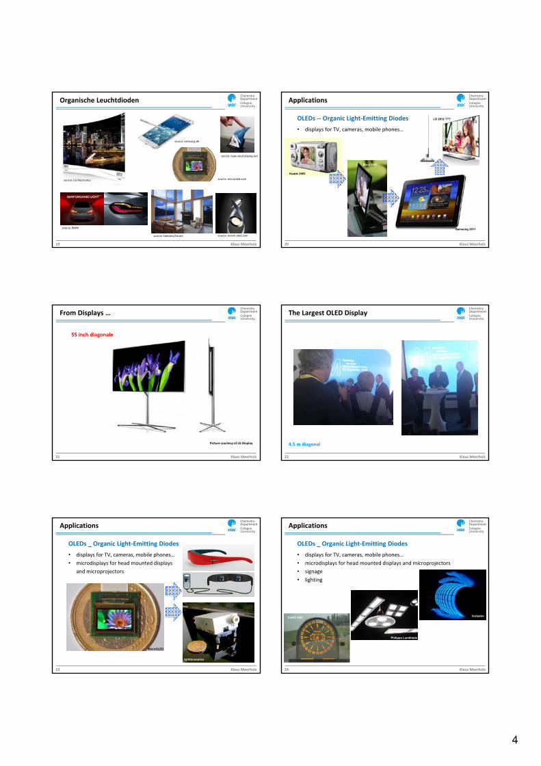
19 Klaus Meerholz
DepartmentCologneUniversity
Chemistry
Organische Leuchtdioden
source: LG Electronics
source: BMW
source: news.oled‐display.net
source: osram‐oled.com
source: samsung.de
source: Siemens/Osram
source: microoled.com
20 Klaus Meerholz
DepartmentCologneUniversity
Chemistry
Sony 2007
Applications
OLEDs ‐‐ Organic Light‐Emitting Diodes
• displays for TV, cameras, mobile phones…
LG 2012 ???
Kodak 2003
Samsung 2011
21 Klaus Meerholz
DepartmentCologneUniversity
Chemistry
From Displays …
Picture courtesy of LG Display
55 inch diagonale
22 Klaus Meerholz
DepartmentCologneUniversity
Chemistry
The Largest OLED Display
4.5 m diagonal
23 Klaus Meerholz
DepartmentCologneUniversity
Chemistry
Applications
OLEDs _ Organic Light‐Emitting Diodes
• displays for TV, cameras, mobile phones…
• microdisplays for head mounted displays
and microprojectors
MicroOLED
lightblueoptics
24 Klaus Meerholz
DepartmentCologneUniversity
Chemistry
Applications
OLEDs _ Organic Light‐Emitting Diodes
• displays for TV, cameras, mobile phones…
• microdisplays for head mounted displays and microprojectors
• signage
• lighting
CARO 2007Verbatim
Philipps Lumiblade

5
25 Klaus Meerholz
DepartmentCologneUniversity
Chemistry
…to Illumination
Pictures courtesy of Osram, Philips
Lumiblade
26 Klaus Meerholz
DepartmentCologneUniversity
Chemistry
Applications
OLEDs ‐‐ Organic Light‐Emitting Diodes
• displays for TV, cameras, mobile phones…
• microdisplays for head mounted displays and microprojectors
• signage
• lighting
State‐of‐the‐art
• small displays in mobile phones, car radios, mp3‐player, …
• TV 15“, 1000€
Dec. 2012?? 55“, ca. 8000€
• microdisplays in HMD
• flexible displays: only prototypes
• lighting: only in designer unique pieces
(expensive)UDC 2012
27 Klaus Meerholz
DepartmentCologneUniversity
Chemistry
hole collecting contact (HCC)
substrate
electron collecting contact (ECC)
hole collecting contact (HCC)
substrate
electron collecting contact (ECC)
acceptor
donor
Organic Solarzellen
1. Exzitonerzeugung & Transport
2. Exzitondissoziierung
3. Freie Ladungsträger, Transport
4. Ladungsextraktion
h
hole colle
cting
contact
electron colle
cting
contact
1.
2.
3.
4.
4.
energy
-
+
+-
3.
donor acceptor
-
+-+
- +
h
+
-
bulk heterojunction (BHJ)planar heterojunction (PHJ)
active layer
Ca. 100 nm
28 Klaus Meerholz
DepartmentCologneUniversity
Chemistry
Organische Solarzellen
source: sargosis.com
source: imec.be & vtt.fi
source: holstcentre.com
source: plusplasticelectronics.com source: G24i
29 Klaus Meerholz
DepartmentCologneUniversity
Chemistry
Applications
OSC _ Organic Solar Cells
• energy production: exploitation of unused surfacesPhotos: Konarka, Heliatek, BMBF
30 Klaus Meerholz
DepartmentCologneUniversity
Chemistry
OSC _ Organic Solar Cells
• energy production: exploitation of unused surfaces
• energy source for mobile phones, cameras, mp3‐player, …
Applications
sunbag, Neuber
solar jacket, Scottevest
printed OSC, Konarka
State‐of‐the‐art
• efficiency in laboratories: 10.7% (Heliatek, Dresden)
• module efficiencies: ca. 3%
• first niche products
• demonstration of prototypes for flexible and transparent apps
6
31 Klaus Meerholz
DepartmentCologneUniversity
Chemistry
Organic semiconductors
1906 dark and photoconductivity of anthracene
1960s electroluminescence of anthracene (50‐2000 V)
1977 doping is possible in organic semiconductors
(Nobel prize for Chemistry in 2000)
1980s first efficient organic solar cell
1987 OLED via evaporation of small molcules
1990 OLED via spin‐coating of polymer layers
2007 11 inch OLED display XEL‐1 by SONY
…
A brief history…
32 Klaus Meerholz
DepartmentCologneUniversity
Chemistry
aus: M. Rehahn,
ChiuZ, 37, 2003, 18.
33 Klaus Meerholz
DepartmentCologneUniversity
Chemistry
Ende 1
34 Klaus Meerholz
DepartmentCologneUniversity
Chemistry
General device stack: OLED & OPV
„bottom“‐contact (ITO, metall grids)
„top“‐contact (Ca/Ag, Ba/Ag, Al, ….)
active layer (mono‐, oligo‐, polymer, mixed systems, …)
hole‐injection or hole‐collection (Pedot, MoO3, …)
substrate (glass, PET, …)
• active layer: ca. 100 nm
• complete device: (w/o substrate) ca. 400‐500 nm thickness of the device is mainly determined by the substrate
35 Klaus Meerholz
DepartmentCologneUniversity
Chemistry
• Injektion
• Transport
• Rekombination
OLED
Anode
Kathode
Emitter
Ca. 100 nm
36 Klaus Meerholz
DepartmentCologneUniversity
Chemistry
hole collecting contact (HCC)
substrate
electron collecting contact (ECC)
hole collecting contact (HCC)
substrate
electron collecting contact (ECC)
acceptor
donor
Organic Solarzellen
1. Exzitonerzeugung & Transport
2. Exzitondissoziierung
3. Freie Ladungsträger, Transport
4. Ladungsextraktion
h
hole colle
cting
contact
electron colle
cting
contact
1.
2.
3.
4.
4.
energy
-
+
+-
3.
donor acceptor
-
+-+
- +
h
+
-
bulk heterojunction (BHJ)planar heterojunction (PHJ)
active layer
Ca. 100 nm

7
37 Klaus Meerholz
DepartmentCologneUniversity
Chemistry
Organic semiconductors
1906 dark and photoconductivity of anthracene
1960s electroluminescence of anthracene (50‐2000 V)
1977 doping is possible in organic semiconductors
(Nobel prize for Chemistry in 2000)
1980s first efficient organic solar cell
1987 OLED via evaporation of small molcules
1990 OLED via spin‐coating of polymer layers
2007 11 inch OLED display XEL‐1 by SONY
…
A brief history…
38 Klaus Meerholz
DepartmentCologneUniversity
Chemistry
aus: M. Rehahn,
ChiuZ, 37, 2003, 18.
39 Klaus Meerholz
DepartmentCologneUniversity
Chemistry
• two major classes of organic semiconductors
– polymers, deposited via spin‐coating
– low‐molecular weight materials, deposited via evaporation
From: Organic Semiconductors, W. Brütting, in: Encyclopedia of Physics, (2005)
Organic Semiconductors, ‐electron systems
40 Klaus Meerholz
DepartmentCologneUniversity
Chemistry
‐electron systems
• two major classes of organic semiconductors
– polymers, deposited via spin‐coating
– low‐molecular weight materials, deposited via evaporation
• both with a conjugated ‐electron system:
formed by pz‐orbitals of sp2‐hybridized C atoms
From: Paula Yurkanis Bruice, „Organic Chemistry“, Pearson
sp2 hybridization
41 Klaus Meerholz
DepartmentCologneUniversity
Chemistry
‐electron systems
• two major classes of organic semiconductors
– polymers, deposited via spin‐coating
– low‐molecular weight materials, deposited via evaporation
• both with a conjugated ‐electron system:
formed by pz‐orbitals of sp2‐hybridized C atoms
From: Paula Yurkanis Bruice, „Organic Chemistry“, Pearson
sp2 hybridization
42 Klaus Meerholz
DepartmentCologneUniversity
Chemistry
From: Grundlagen der organischen Halbleiter, W. Brütting, W. Rieß, Physik Journal 7(5) (2008)
‐electron systems
• two major classes of organic semiconductors
– polymers, deposited via spin‐coating
– low‐molecular weight materials, deposited via evaporation
• both with a conjugated ‐electron system:
formed by pz‐orbitals of sp2‐hybridized C atoms
simplest example: ethene = C2H4

8
43 Klaus Meerholz
DepartmentCologneUniversity
Chemistry
Extended ‐systemexample: benzene = C6H6
‐electron systems
Benzenemolecular formula
BenzeneKekulé constitutional formula
Benzeneplanar hexagon
Benzenesp 2 form ‐bondings
Benzene6 p‐orbitals
Benzenedelocalized ‐orbitals
Benzenesimplified illustration
LUMO
HOMO
44 Klaus Meerholz
DepartmentCologneUniversity
Chemistry
…. depend on the electronic structure of
• (single) molecules • molecular geometry
• molecular aggregation• 3D packing
Most important:Delocalizable electrons
-electronsmolecular orbitals
Optical & Electrical Properties ….
45 Klaus Meerholz
DepartmentCologneUniversity
Chemistry
‐electron systems
Polymer conformation
From: Collini and Scholes Science, 323, (2009) 369.
46 Klaus Meerholz
DepartmentCologneUniversity
Chemistry
‐electron systems
Polymer conformation
From: Dyakonov, Seminar Experimental Physics 2011
polymer segment with different conjugation length different energy states dep. on conjugation length & on the surrounding
47 Klaus Meerholz
DepartmentCologneUniversity
Chemistry
Optical Properties
48 Klaus Meerholz
DepartmentCologneUniversity
Chemistry
occupied orbitals
unoccupied orbitals
LUMO
lowest unoccupied molecular orbital
HOMOhighest occupied molecular orbital
}
}refractive index
linear regimePOLARIZATION
Optical Properties (real part)
LCD Anzeige

9
49 Klaus Meerholz
DepartmentCologneUniversity
Chemistry
occupied orbitals
unoccupied orbitals
LUMO
lowest unoccupied molecular orbital
HOMOhighest occupied molecular orbital
}
}
(linear)
absorption
Optical Properties (imaginary part)
Solarzelle
50 Klaus Meerholz
DepartmentCologneUniversity
Chemistry
occupied orbitals
unoccupied orbitals
LUMO
lowest unoccupied molecular orbital
HOMOhighest occupied molecular orbital
}
}luminescence
Emission
51 Klaus Meerholz
DepartmentCologneUniversity
Chemistry
‐electron systems
E
E0
LUMO
HOMO
200nm290nm
380nm525nm
Extended ‐system
52 Klaus Meerholz
DepartmentCologneUniversity
Chemistry
aus:
Hesse, Meier, Zeeh, Spektroskopische Methoden in der organischen Chemie, Thieme Verlag 1991
53 Klaus Meerholz
DepartmentCologneUniversity
Chemistry
well‐defined spin states: excitons tightly bound and localized on one molecule
Optical properties
Jablonski diagram
54 Klaus Meerholz
DepartmentCologneUniversity
Chemistry
Potential curve and resulting spectra
r
pot. E
S0
T1
S1
ISC
h
I
E
Ph
FL abs
Optical properties
ground state
excited states
vibrational levels

10
55 Klaus Meerholz
DepartmentCologneUniversity
Chemistry
aus: M. Pope, C. E. Swenberg, Electronic Processes in Organic Crystals and Polymers Oxford University Press, New York 1999.
56 Klaus Meerholz
DepartmentCologneUniversity
Chemistry
Optische Spektren konjugierter Moleküle
57 Klaus Meerholz
DepartmentCologneUniversity
Chemistry
‐electron systems
Color variation
400 500 700 700
[nm]
400 500 700 700
emission wavelength
N
OBe
N
OBeBq2
Eu
S
O
CF3
O
3S
N
O NO
O
NC CN
N
O
OZn
N
O
O
n nN
O
O
n
HN
NN
NH
Perylen
Coumarin 6
Zn(oxz)n
Polyfluoren
Rubren
TPP
MEH-PPVDCM
Eu(TTA)3phen
PPV
polymere emitter
58 Klaus Meerholz
DepartmentCologneUniversity
Chemistry
Charge Transport
59 Klaus Meerholz
DepartmentCologneUniversity
Chemistry
occupied orbitals
unoccupied orbitals
LUMO
lowest unoccupied molecular orbital
HOMOhighest occupied molecular orbital
}
} oxidationp-doping
hole generation
reductionn-doping
electron generation
Redox Activity / Doping
Elektrochromie
60 Klaus Meerholz
DepartmentCologneUniversity
Chemistry
Charge transport in OS
„p‐type“ _ hole transport
occupied orbitals
unoccupied orbitalsLUMO
lowest unoccupied molecular orbital
HOMOhighest occupied molecular orbital
}
}anode cathode

11
61 Klaus Meerholz
DepartmentCologneUniversity
Chemistry
Photoconductors (p‐type)
Charge transport in OS
„electron rich system“
From Rubipy Scientific inc.
62 Klaus Meerholz
DepartmentCologneUniversity
Chemistry
Charge transport in OS
„n‐type“ _ electron transport
occupied orbitals
unoccupied orbitalsLUMO
lowest unoccupied molecular orbital
HOMOhighest occupied molecular orbital
}
}anode cathode
63 Klaus Meerholz
DepartmentCologneUniversity
Chemistry
Photoconductors (n‐type)
Charge transport in OS
„electron poor system“
From Rubipy Scientific inc.
64 Klaus Meerholz
DepartmentCologneUniversity
Chemistry
Charge transport in OS
„Hopping“ transport in amorphous solids
field [V/m]
e-
h+
e-
M M M M MMhole transport
electron transport M M M M MM
charge carriers are radical ions
problem: they react with oxygen, water and other impurities
65 Klaus Meerholz
DepartmentCologneUniversity
Chemistry
Charge transport in OS
DOS of energetic states
E
EF
EF
ano
de
org
anic
cath
od
e
E
ano
de
cath
od
e
LUMO
HOMO
e
h
org
anic
hEL
2
1a
1b
3
E
DOS
„Hopping transport“
66 Klaus Meerholz
DepartmentCologneUniversity
Chemistry
Charge transport in OS
DOS of energetic states
From: ChemPhysChem, 9, (2008), 666
Bässler model _ hopping transport in amorphous solids
12
67 Klaus Meerholz
DepartmentCologneUniversity
Chemistry
OLED bzw. OPV
OLED
• Injektion von Ladungsträgern
• Transport
• Rekombination
• Exzitonenbildung
• Emission
OLED
LEC
OPV
• Extraktion von Ladungsträgern
• Transport
• Dissoziation
• Exzitonenbildung
• Absorption
Bulk heterojunction
Grätzel Zelle


![· Web viewStruktur-Eigenschafts-Beziehungen, 4. Chemisches Gleichgewicht, 5. Säure-Base-Reaktionen, 6. Redoxreaktionen, 7. Komplex-reaktionen, 8. Energie [2]. Zu diesen Basiskonzepten](https://img.pdfslide.org/doc/110x75/5cd812ab88c993515c8dd889/-web-viewstruktur-eigenschafts-beziehungen-4-chemisches-gleichgewicht-5-saeure-base-reaktionen.jpg)


![Symbole für die betriebliche Praxis · Elektrostatisch gefährdetes Bauteil Energieeffizienzetikett: [Elektrogeräte] [Autoreifen] Energiesparlampe Energieverbrauchsetikett Energystar](https://img.pdfslide.org/doc/110x75/5e1eb0697e3d941f651fb1d5/symbole-fr-die-betriebliche-praxis-elektrostatisch-gefhrdetes-bauteil-energieeffizienzetikett.jpg)