Embed Size (px)
Citation preview

Integrierte Hard- und Softwaresysteme
IHS 3: Test of Digital Systems
R.Ubar, A. Jutman, H-D. Wuttke

Technical University Tallinn, ESTONIACopyright 2000-2003 by Raimund Ubar
2
Organisatorisches
Nächste Termine: 4.2./5.2. 10:00 Blockveranstaltung Dr. Jutman 7.2./8.2. 10:00 Blockveranstaltung Dr. Jutman
Raum: Rechner-Pool H 1501

Technical University Tallinn, ESTONIACopyright 2000-2003 by Raimund Ubar
3
Experiments
• Use the example A+B/2 (avarage value)• Find for each test method best parameters
– Functional test– Deterministic test– Functional BIST– Logical BIST– Circular BIST
• Note them and compare results

Technical University Tallinn, ESTONIACopyright 2000-2003 by Raimund Ubar
4
Ad Hoc Design for Testability TechniquesMethod of Test Points:
Block 1 Block 2Block 1 is not observable,Block 2 is not controllable
Block 1 Block 21
CP1
Improving controllability:
Block 1 Block 2
Normal working mode:CP1 = 0, CP2 = 1 Controlling Block 2 with 1:CP1 = 1, CP2 = 1Controlling Block 2 with 0:CP2 = 0
MUX
CP1
&
CP2
CP2
Normal working mode:CP2 = 0 Controlling Block 2 with 1:CP1 = 1, CP2 = 1Controlling Block 2 with 0:CP1 = 0, CP2 = 1

Technical University Tallinn, ESTONIACopyright 2000-2003 by Raimund Ubar
5
Scan-Path Design
Combinational circuit
IN OUT
R
Scan-IN
Scan-OUT
1&&
q
q’Scan-IN
T
TDC
Scan-OUT
q
q’
Scan-Path design allows to control and observe internal flip-flops, which means that the task of sequential testing has been transformed to the task of testing a combinational circuit
T = 0 - normal working mode T = 1 - scan mode
Normal mode : flip-flops (R) are connected to the combinational circuit
Test mode: flip-flops are disconnected from the combinational circuit and connected to each other to form a shift register

Technical University Tallinn, ESTONIACopyright 2000-2003 by Raimund Ubar
6
Scan-Path Design and Testability
OUTMUX
DMUXIN
SCANOUT
SCANIN
Two possibilities for improving controllability/observability
Technical University Tallinn, ESTONIACopyright 2000-2003 by Raimund Ubar
7
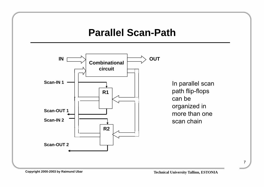
Parallel Scan-Path
Combinational circuit
IN OUT
R1
Scan-IN 1
Scan-OUT 1
R2
Scan-IN 2
Scan-OUT 2
In parallel scan path flip-flops can be organized in more than one scan chain

Technical University Tallinn, ESTONIACopyright 2000-2003 by Raimund Ubar
8
Boundary Scan Standard

Technical University Tallinn, ESTONIACopyright 2000-2003 by Raimund Ubar
9
Boundary Scan Standard
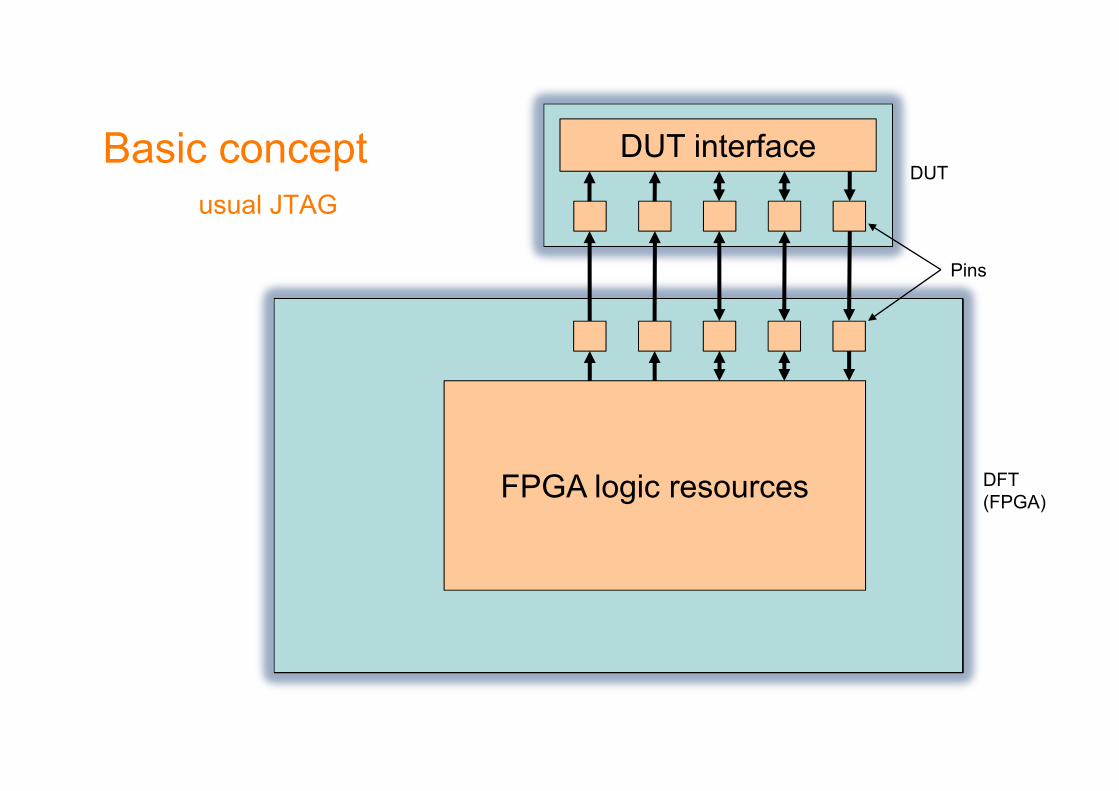
Basic conceptusual JTAG
FPGA logic resources DFT(FPGA)
DUT interfaceDUT
Pins

Basic conceptusual JTAG
FPGA logic resources
DUT interface
TDI
TDO
TAP
Con
trolle
r
DUT
DFT(FPGA)
BScan cells
BScan chain

TAP
Con
trolle
r
FPGA logic resources
010
Basic conceptusual JTAG
DUT interface
TDI
TDO
011101011001*0101
1
0101
DUT
DFT(FPGA)
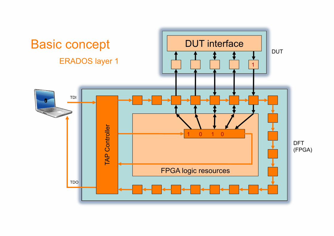
Basic conceptERADOS layer 1
FPGA logic resources
DUT interface
TDI
TDO
TAP
Con
trolle
r*0101
1 0 1 0
1
DUT
DFT(FPGA)
FPGA logic resources
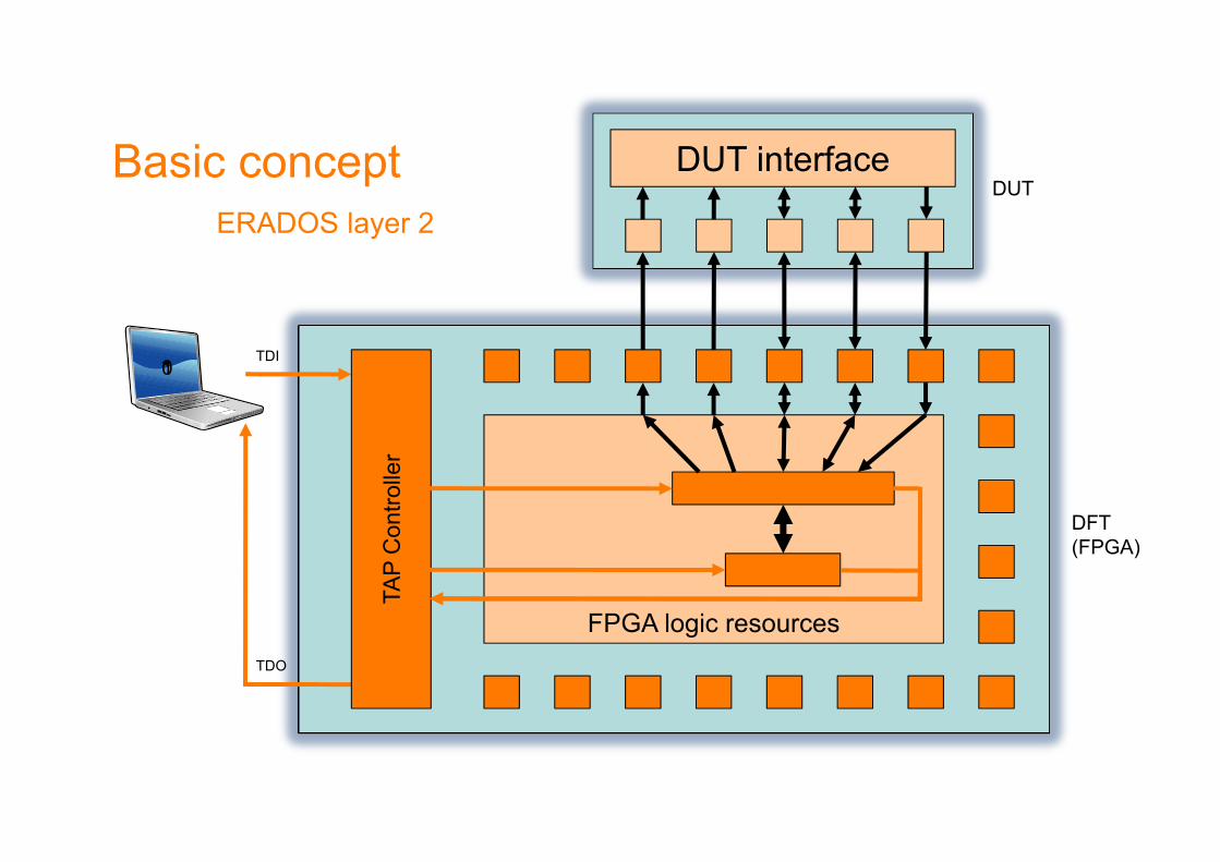
Basic conceptERADOS layer 2
DUT interface
TDI
TDO
TAP
Con
trolle
r*10
DUT
DFT(FPGA)

FPGA logic resources
Basic conceptERADOS layer 2
DUT interface
TDI
TDO
0 1
1
TAP
Con
trolle
r
1 0 1 0
1
0 1 *
DUT
DFT(FPGA)

FPGA logic resources
Basic conceptERADOS higher layers
DUT interface
TDI
TDO
TAP
Con
trolle
r impl. of layers 1 - 3
DUT
DFT(FPGA)diagnostic processor
(layer 4 – 5)

Technical University Tallinn, ESTONIACopyright 2000-2003 by Raimund Ubar
17
Texas Instruments SCOPE™ Family of Testability
SCOPE™ Instruction Set:
– IEEE Standard 1149.1-1990 Required Instructions,
– Optional INTEST, CLAMP and HIGHZ
– Parallel-Signature Analysis at Inputs
– Pseudo-Random Pattern Generation From Outputs
– Sample Inputs/Toggle Outputs
– 4-wire test access port (TAP) interface

Technical University Tallinn, ESTONIACopyright 2000-2003 by Raimund Ubar
18
Boundary Scan Standard 1149.1-1990
Serial-test information is conveyed by means of a 4-wire test bus, or TAP, that conforms to IEEE Standard 1149.1-1990
Test instructions, test data, and test control signals all are passed along this serial-test bus.
The TAP controller monitors two signals from the test bus, TCK and TMS.

Technical University Tallinn, ESTONIACopyright 2000-2003 by Raimund Ubar
19
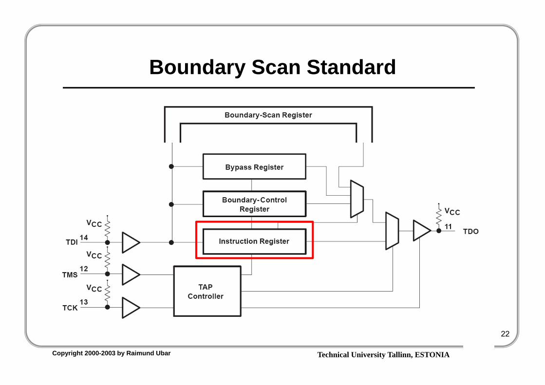
Mandatory features
• Test Access Port (TAP):– TCK (Test Clock), TMS (Test Mode Selection), – TDI (Test Data In), and TDO (Test Data Out)
• TAP Controller (FSM)• Instruction Register (2 bit or more)• Bypass Register (1 bit)• Boundary Scan Register (1 bit or more)

Technical University Tallinn, ESTONIACopyright 2000-2003 by Raimund Ubar
20
Boundary Scan Register

Technical University Tallinn, ESTONIACopyright 2000-2003 by Raimund Ubar
21
Boundary Scan Standard
Technical University Tallinn, ESTONIACopyright 2000-2003 by Raimund Ubar
22
Boundary Scan Standard

Technical University Tallinn, ESTONIACopyright 2000-2003 by Raimund Ubar
23
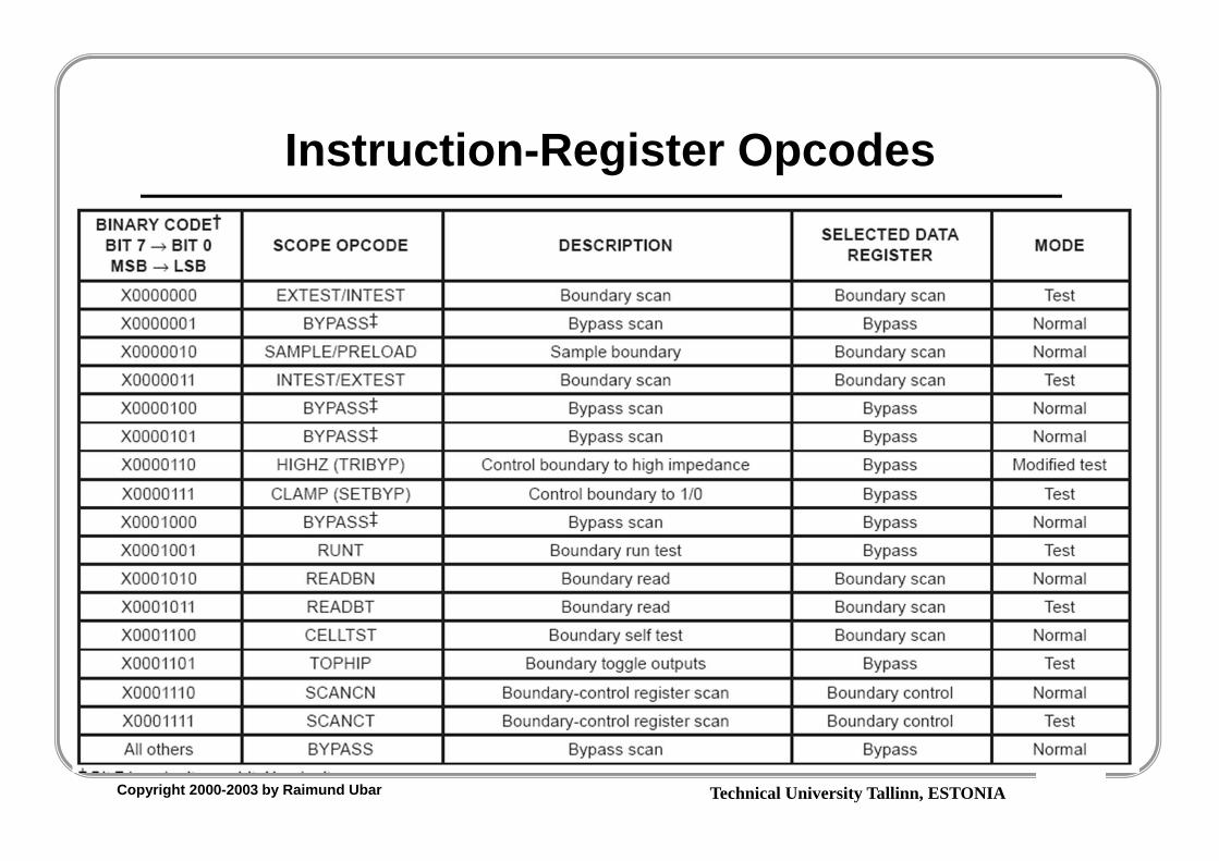
Instruction-Register Opcodes

Technical University Tallinn, ESTONIACopyright 2000-2003 by Raimund Ubar
24
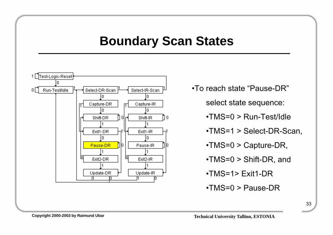
TAP-controller state diagram
Technical University Tallinn, ESTONIACopyright 2000-2003 by Raimund Ubar
25
Instruction-Register Opcodes

Technical University Tallinn, ESTONIACopyright 2000-2003 by Raimund Ubar
26
STEP0: After Switch on
• Scan Chain in off
•BS cells are inactive
•Goal:
•Test connection between
Pin AB2 of U1 and Pin 15 of U2
Technical University Tallinn, ESTONIACopyright 2000-2003 by Raimund Ubar
27
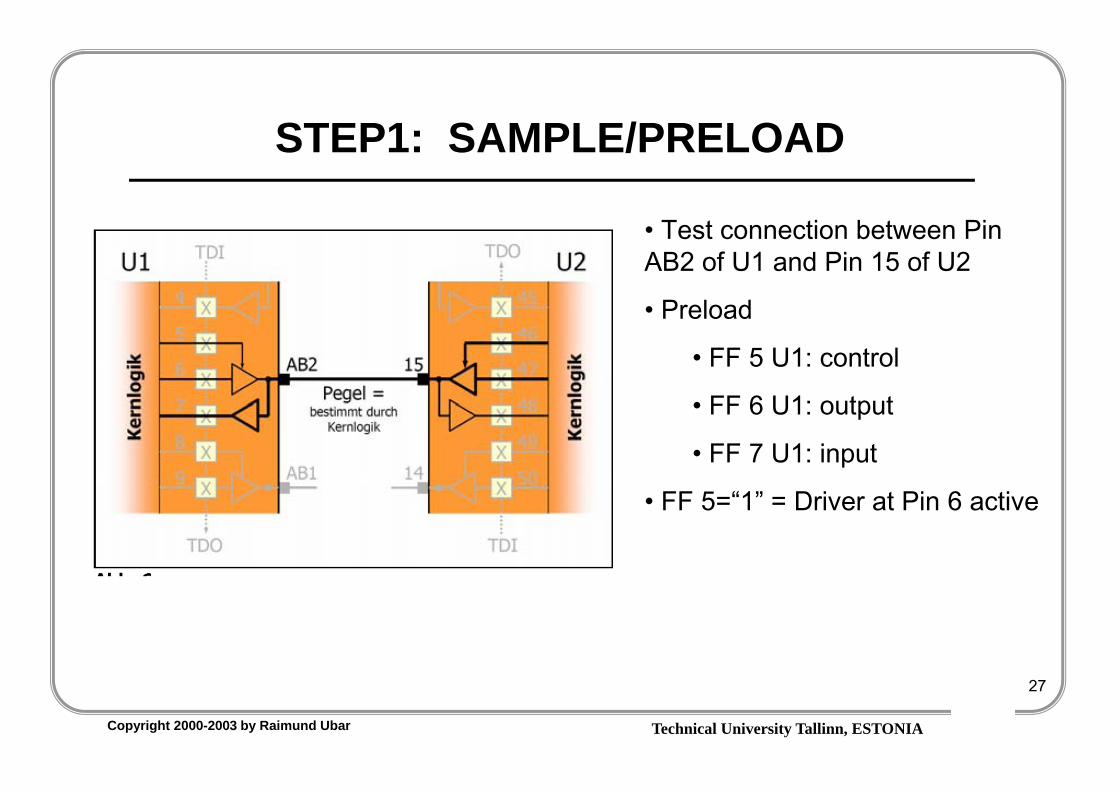
STEP1: SAMPLE/PRELOAD
• Test connection between Pin AB2 of U1 and Pin 15 of U2
• Preload
• FF 5 U1: control
• FF 6 U1: output
• FF 7 U1: input
• FF 5=“1” = Driver at Pin 6 active

Technical University Tallinn, ESTONIACopyright 2000-2003 by Raimund Ubar
28
STEP2: SAMPLE/PRELOAD
• Driving AB2 of U1 with “1”
• Scan chain is activated
• Scan cells are inactive (x)

Technical University Tallinn, ESTONIACopyright 2000-2003 by Raimund Ubar
29
STEP3: EXTEST
• Test vector loaded
• Scan cells active
• Pin 6 U1 drives “1”
• Pin 15 U2: tri state (inactive)
• Measuring
• U1: at cell 7
• U2 at cell 48

Technical University Tallinn, ESTONIACopyright 2000-2003 by Raimund Ubar
30
STEP4: SCAN DR
•Read AB2 at Pin 15
• result in cell 48 and 7
• Shift (new test vector)
• Drive new values

Technical University Tallinn, ESTONIACopyright 2000-2003 by Raimund Ubar
31
Calculation
• 500 BS-cells• TCK frequency: 10 MHz• Shift operation: 50 μs = 1 signal change• 2 edges = 2 shifts• What is the frequency for changing the value at a
pin?• 500 cells a 2 shifts => 1000 shifts until next value• => frequency 10 kHz• => Bottleneck

Technical University Tallinn, ESTONIACopyright 2000-2003 by Raimund Ubar
32
Boundary Scan Applet
Technical University Tallinn, ESTONIACopyright 2000-2003 by Raimund Ubar
33
Boundary Scan States
•To reach state “Pause-DR”
select state sequence:
•TMS=0 > Run-Test/Idle
•TMS=1 > Select-DR-Scan,
•TMS=0 > Capture-DR,
•TMS=0 > Shift-DR, and
•TMS=1> Exit1-DR
•TMS=0 > Pause-DR

Technical University Tallinn, ESTONIACopyright 2000-2003 by Raimund Ubar
34
Boundary Scan Diagnosis

Technical University Tallinn, ESTONIACopyright 2000-2003 by Raimund Ubar
35
References
• Books:• Boundary Scan Handbook, 3rd Edition, Ken P. Parker,
Kluwer Academic Publishers, ISBN 1-4020-7496-4• Analog and Mixed-Signal Boundary-Scan, Adam Osseiran,
Kluwer Academic Publishers, ISBN 0-7923-8686-8• Digital Systems Testing and Testable Design, Miron
Abramovici et.al., IEEE Press, Wiley Interscience, ISBN 0-7803-1093-4
• Websites:• www.goepelusa.com• www.freeDFT.info• www.DFTdigest.com• www.smta.org
Technical University Tallinn, ESTONIACopyright 2000-2003 by Raimund Ubar
36
Organisatorisches
Nächste Termine: 4.2./5.2. 10:00 Blockveranstaltung Dr. Jutman 7.2./8.2. 10:00 Blockveranstaltung Dr. Jutman
Raum: Rechner-Pool H 1501