Embed Size (px)
Citation preview
Fachgebiet 3D-Nanostrukturierung, Institut für Physik
Contact: [email protected]; [email protected]
Office: Unterpoerlitzer Straße 38 (Heisenbergbau) (tel: 3748) http://www.tu-ilmenau.de/3dnanostrukturierung/
Vorlesung: Thursday 7:00 – 8:30, F 3001 (Faradaybau)
Übung: Friday (G), 11:00 – 12:30, C 110
Prof. Yong Lei & Dr. Yang Xu
(a) (b2) (b1)
UTAM-prepared free-standing one-dimensional surface nanostructures on Si
substrates: Ni nanowire arrays (a) and carbon nanotube arrays (b).
Nanostrukturphysik (Nanostructure Physics)

• Class 1: A general introduction of fundamentals of nano-structured materials
• Class 2: Structures and properties of nanocrystalline materials
• Class 3: Graphene
• Class 4: 2D atomically thin nanosheets
• Class 5: Optical properties of 1D nanostructures and nano-generator
• Class 6: Carbon nanotubes
• Class 7: Solar water splitting I: fundamentals
• Class 8: Solar water splitting II: nanostructures for water splitting
• Class 9: Lithium-ion batteries: Si nanostructures
• Class 10: Sodium-ion batteries and other ion batteries, and Supercapacitors
• Class 11: Solar cells
• Class 12: Other nanostructures
Contents of Class 2
Structures and properties of nanocrystalline materials
New methods & new structures
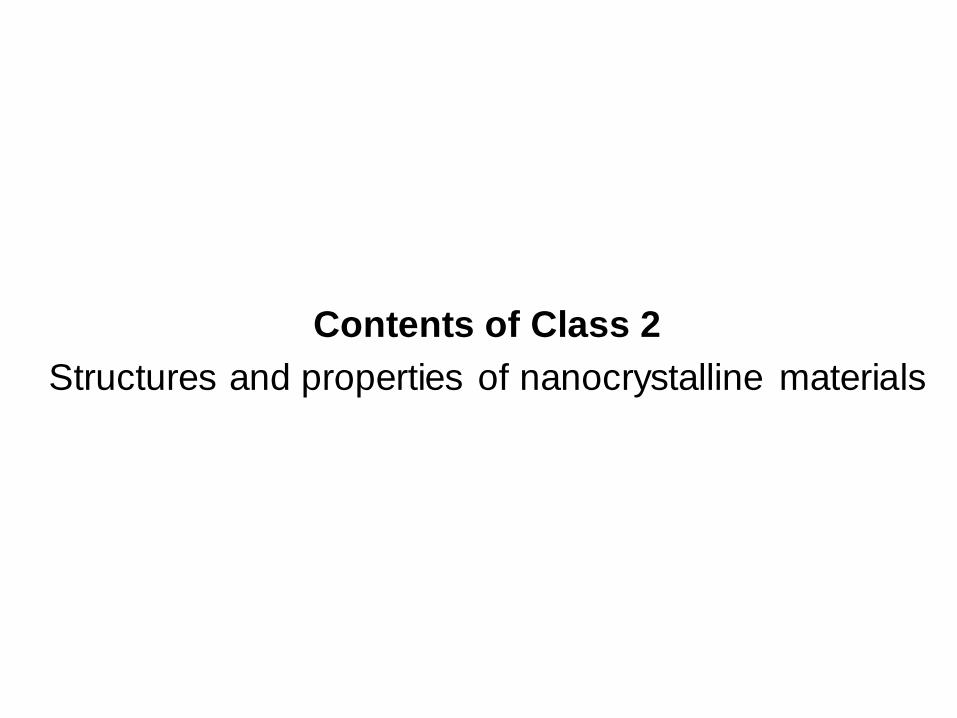
• Developing and applying new methods of investigation
TEM, SEM, STEM, etc. (Techniken der Oberflächenphysik)
• Preparing materials with novel structural features and/or properties
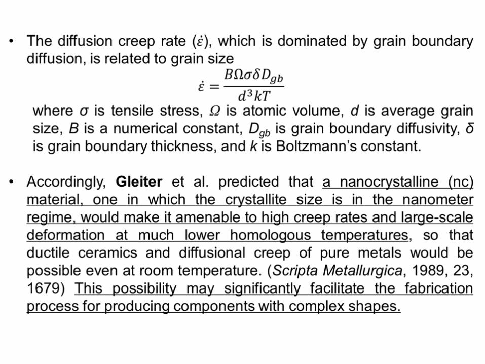
Nanocrystalline materials: solids with new atomic structures and their properties decided by the atomic arrangements in the cores of defects. (Nanostrukturphysik)
Development of solid state physics and material science are made in many cases by one of the following two approaches:
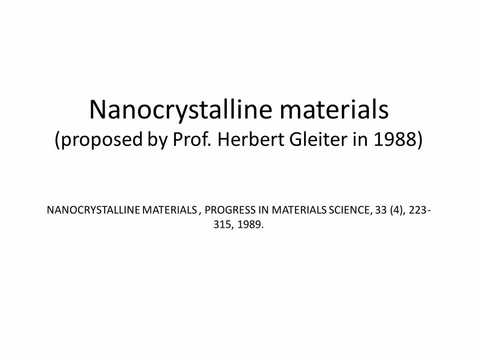
Nanocrystalline materials (proposed by Prof. Herbert Gleiter in 1988)
NANOCRYSTALLINE MATERIALS , PROGRESS IN MATERIALS SCIENCE, 33 (4), 223-315, 1989.
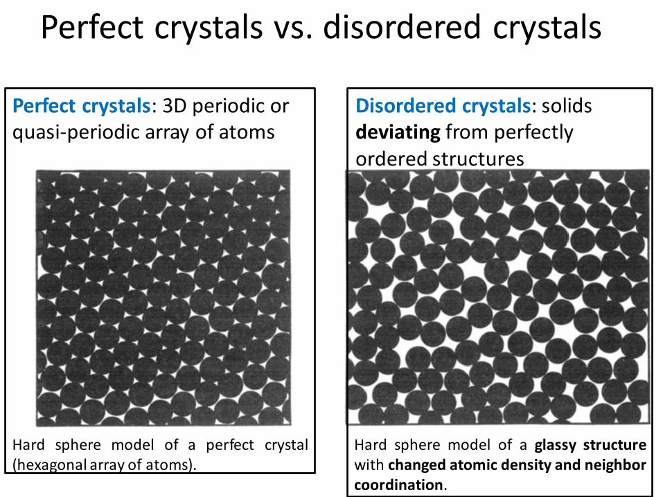
Perfect crystals vs. disordered crystals
Perfect crystals: 3D periodic or quasi-periodic array of atoms
Disordered crystals: solids deviating from perfectly ordered structures
Hard sphere model of a perfect crystal (hexagonal array of atoms).
Hard sphere model of a glassy structure with changed atomic density and neighbor coordination.
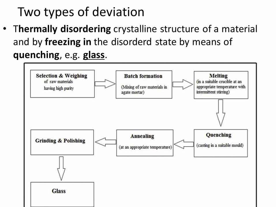
Two types of deviation • Thermally disordering crystalline structure of a material
and by freezing in the disorderd state by means of quenching, e.g. glass.
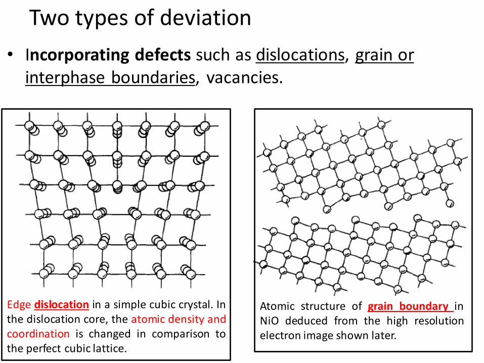
Two types of deviation
• Incorporating defects such as dislocations, grain or interphase boundaries, vacancies.
Edge dislocation in a simple cubic crystal. In the dislocation core, the atomic density and coordination is changed in comparison to the perfect cubic lattice.
Atomic structure of grain boundary in NiO deduced from the high resolution electron image shown later.
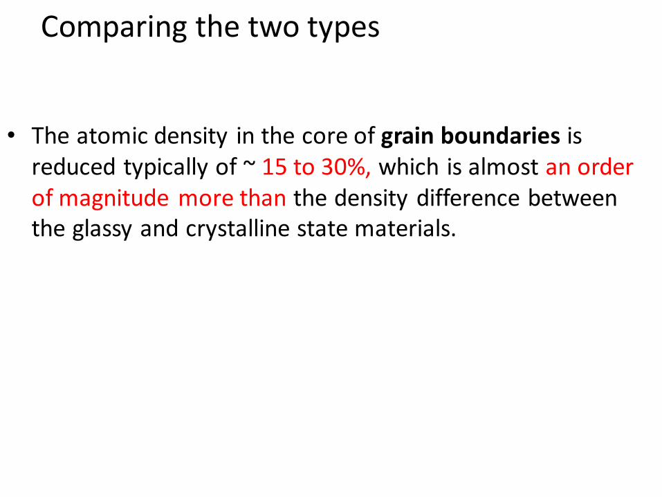
Comparing the two types
• The atomic density in the core of grain boundaries is reduced typically of ~ 15 to 30%, which is almost an order of magnitude more than the density difference between the glassy and crystalline state materials.
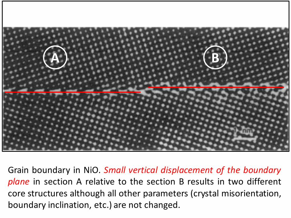
A B
Grain boundary in NiO. Small vertical displacement of the boundary plane in section A relative to the section B results in two different core structures although all other parameters (crystal misorientation, boundary inclination, etc.) are not changed.
What’s like in conventional polycrystals?
Conventional polycrystals: grain size typically ≥ 1 μm
The atomic structures of the boundary cores are not noticed in most structural investigations such as XRD, because the fraction of atoms located in the core of the boundaries is 10-4 or less.
Basic idea of nanocrytalline materials
What if one generates a material that contains a high density of defects?
• Nanocrystalline materials is a new class of disordered solids by introducting such a high density of defect cores that 50% or more of the atoms (molecules) are situated in the core of these defects (typically 1019 per cm3).
• Types of defects: grain boundaries, interphase boundaries, dislocations, etc.
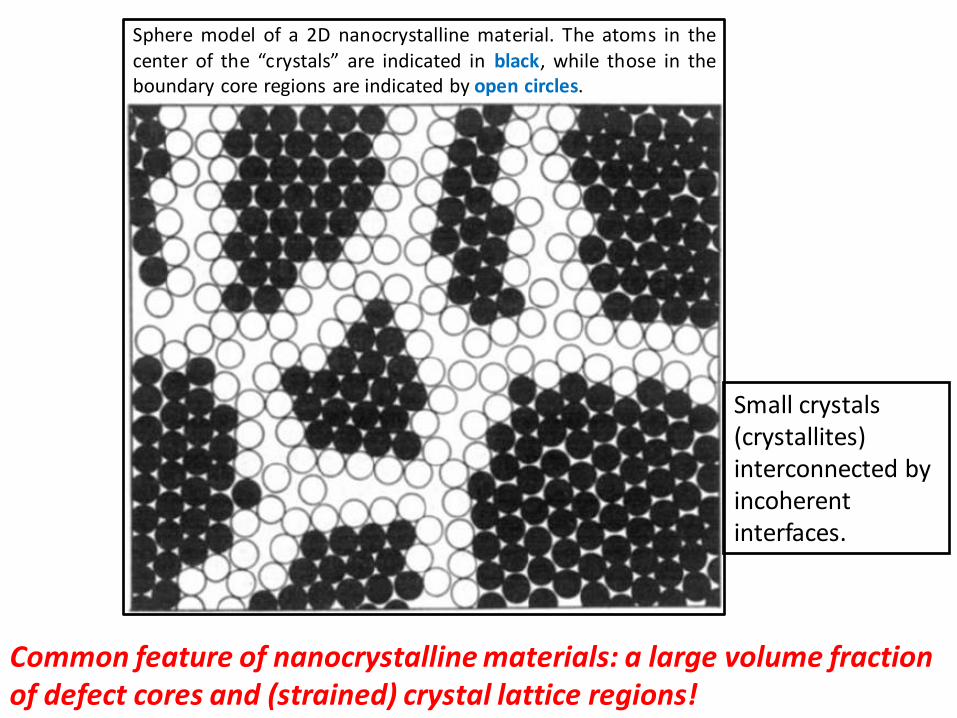
Sphere model of a 2D nanocrystalline material. The atoms in the center of the “crystals” are indicated in black, while those in the boundary core regions are indicated by open circles.
Common feature of nanocrystalline materials: a large volume fraction of defect cores and (strained) crystal lattice regions!
Small crystals (crystallites) interconnected by incoherent interfaces.
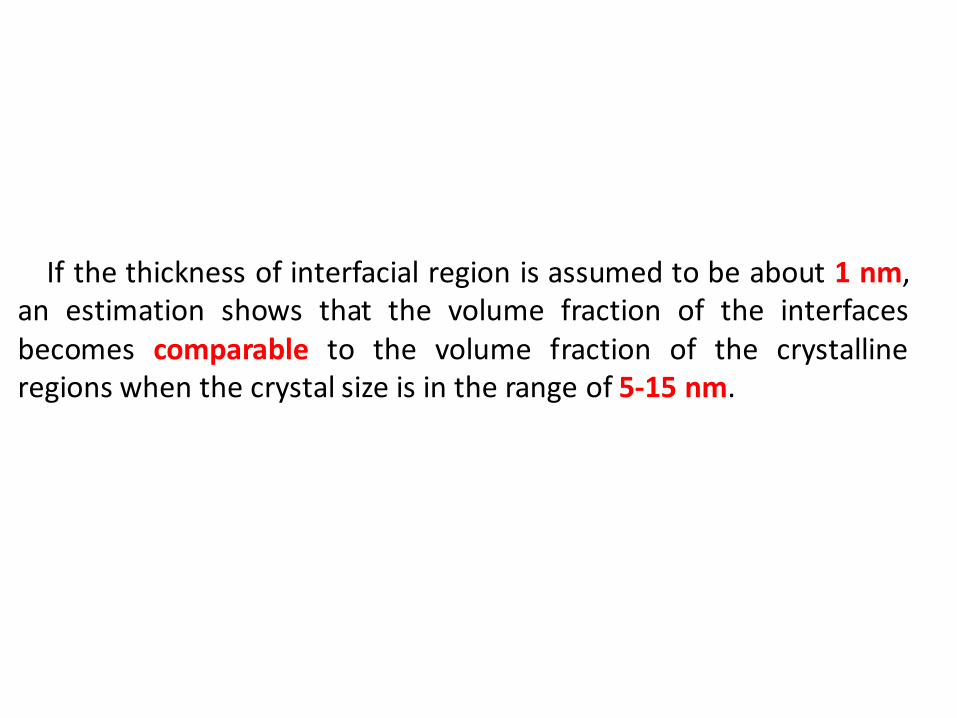
If the thickness of interfacial region is assumed to be about 1 nm, an estimation shows that the volume fraction of the interfaces becomes comparable to the volume fraction of the crystalline regions when the crystal size is in the range of 5-15 nm.
Basic idea of nanocrytalline materials
• Atomic structure of the core regions of different boundaries between crystals are different because their structures depend on the crystal misorientations and boundary inclinations - structure heterogeneity
• This featured structure of heterogeneity is not formed in thermally induced disordered solids such as glasses.
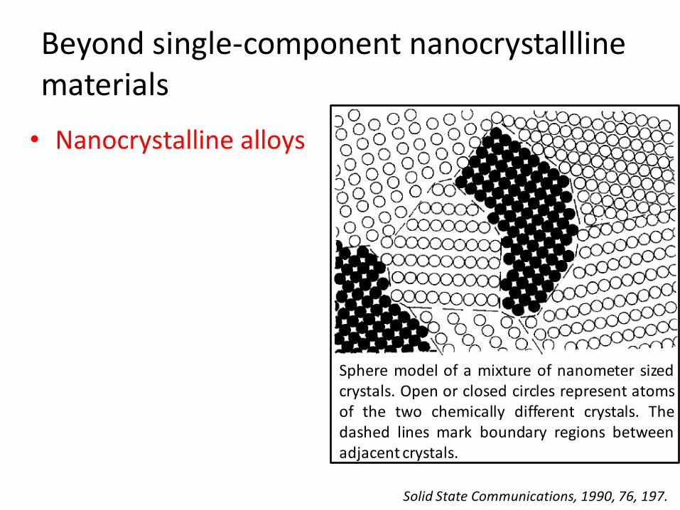
Beyond single-component nanocrystallline materials
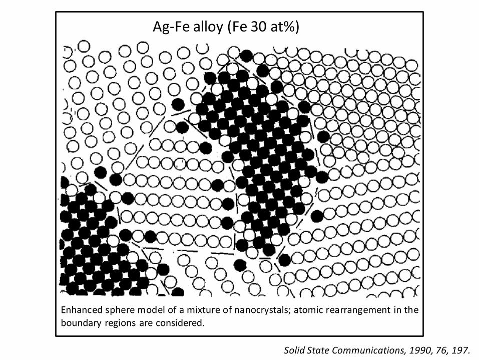
• Nanocrystalline alloys
Sphere model of a mixture of nanometer sized crystals. Open or closed circles represent atoms of the two chemically different crystals. The dashed lines mark boundary regions between adjacent crystals.
Solid State Communications, 1990, 76, 197.
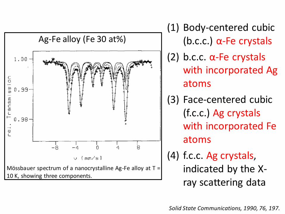
(1) Body-centered cubic (b.c.c.) α-Fe crystals
(2) b.c.c. α-Fe crystals with incorporated Ag atoms
(3) Face-centered cubic (f.c.c.) Ag crystals with incorporated Fe atoms
(4) f.c.c. Ag crystals, indicated by the X-ray scattering data
Ag-Fe alloy (Fe 30 at%)
Mӧssbauer spectrum of a nanocrystalline Ag-Fe alloy at T = 10 K, showing three components.
Solid State Communications, 1990, 76, 197.
Solid State Communications, 1990, 76, 197.
Ag-Fe alloy (Fe 30 at%)
Enhanced sphere model of a mixture of nanocrystals; atomic rearrangement in the boundary regions are considered.
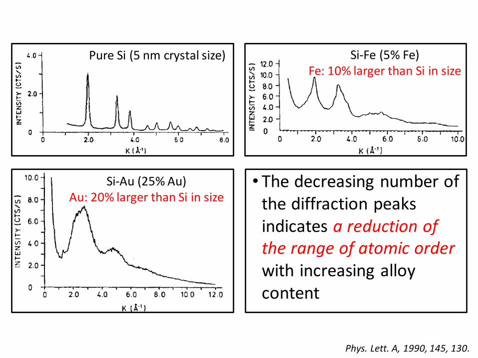
Pure Si (5 nm crystal size) Si-Fe (5% Fe) Fe: 10% larger than Si in size
Si-Au (25% Au) Au: 20% larger than Si in size
• The decreasing number of the diffraction peaks indicates a reduction of the range of atomic order with increasing alloy content
Phys. Lett. A, 1990, 145, 130.
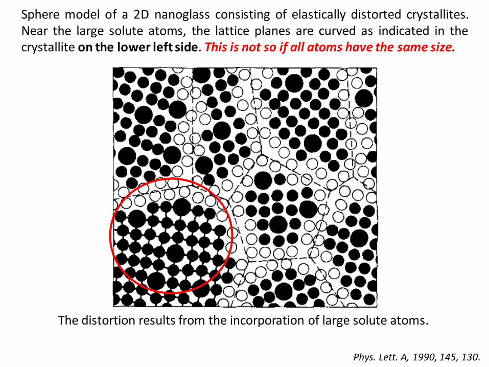
Sphere model of a 2D nanoglass consisting of elastically distorted crystallites. Near the large solute atoms, the lattice planes are curved as indicated in the crystallite on the lower left side. This is not so if all atoms have the same size.
The distortion results from the incorporation of large solute atoms.
Phys. Lett. A, 1990, 145, 130.
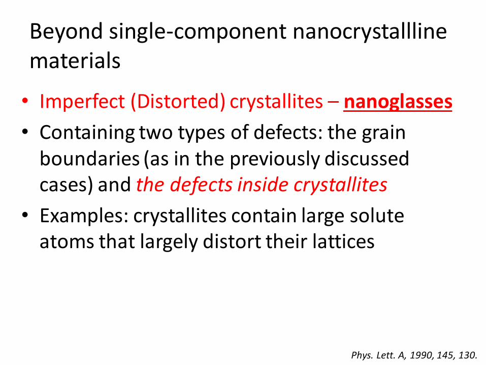
Beyond single-component nanocrystallline materials
• Imperfect (Distorted) crystallites – nanoglasses
• Containing two types of defects: the grain boundaries (as in the previously discussed cases) and the defects inside crystallites
• Examples: crystallites contain large solute atoms that largely distort their lattices
Phys. Lett. A, 1990, 145, 130.
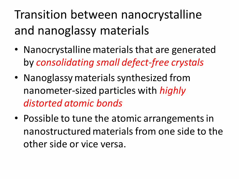
Transition between nanocrystalline and nanoglassy materials
• Nanocrystalline materials that are generated by consolidating small defect-free crystals
• Nanoglassy materials synthesized from nanometer-sized particles with highly distorted atomic bonds
• Possible to tune the atomic arrangements in nanostructured materials from one side to the other side or vice versa.
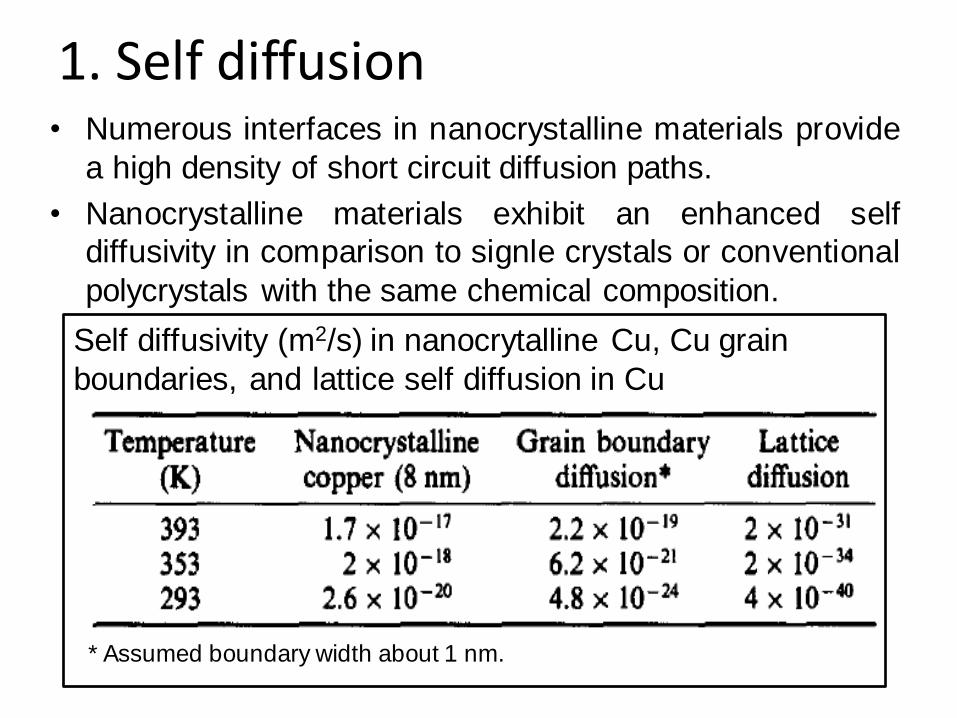
1. Self diffusion • Numerous interfaces in nanocrystalline materials provide
a high density of short circuit diffusion paths.
• Nanocrystalline materials exhibit an enhanced self
diffusivity in comparison to signle crystals or conventional
polycrystals with the same chemical composition.
Self diffusivity (m2/s) in nanocrytalline Cu, Cu grain
boundaries, and lattice self diffusion in Cu
* Assumed boundary width about 1 nm.
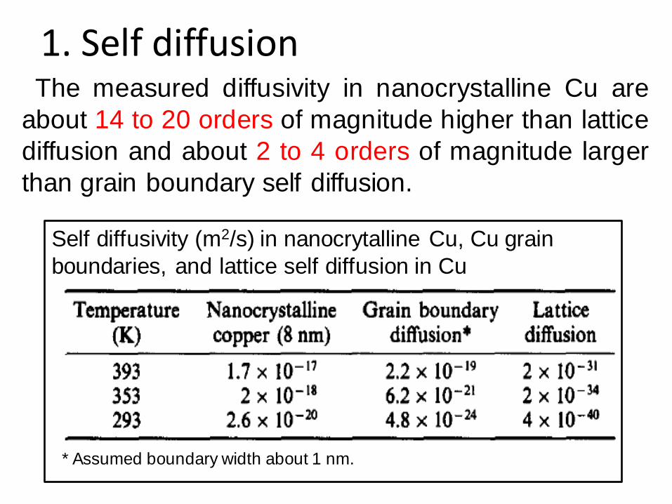
1. Self diffusion
Self diffusivity (m2/s) in nanocrytalline Cu, Cu grain
boundaries, and lattice self diffusion in Cu
* Assumed boundary width about 1 nm.
The measured diffusivity in nanocrystalline Cu are
about 14 to 20 orders of magnitude higher than lattice
diffusion and about 2 to 4 orders of magnitude larger
than grain boundary self diffusion.
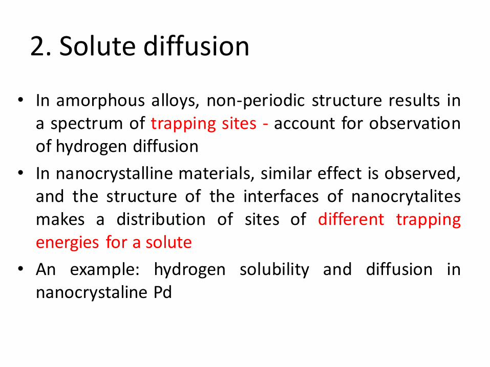
2. Solute diffusion
• In amorphous alloys, non-periodic structure results in a spectrum of trapping sites - account for observation of hydrogen diffusion
• In nanocrystalline materials, similar effect is observed, and the structure of the interfaces of nanocrytalites makes a distribution of sites of different trapping energies for a solute
• An example: hydrogen solubility and diffusion in nanocrystaline Pd
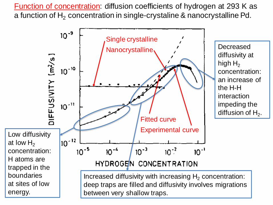
Single crystalline
Nanocrystalline
Fitted curve
Experimental curve
Function of concentration: diffusion coefficients of hydrogen at 293 K as
a function of H2 concentration in single-crystaline & nanocrystalline Pd.
Low diffusivity
at low H2
concentration:
H atoms are
trapped in the boundaries
at sites of low
energy.
Increased diffusivity with increasing H2 concentration:
deep traps are filled and diffusivity involves migrations
between very shallow traps.
Decreased
diffusivity at
high H2
concentration:
an increase of the H-H
interaction
impeding the
diffusion of H2.
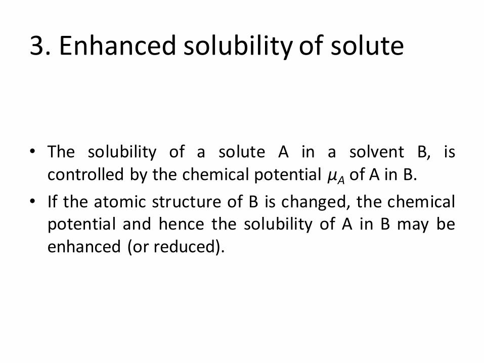
3. Enhanced solubility of solute
• The solubility of a solute A in a solvent B, is controlled by the chemical potential μA of A in B.
• If the atomic structure of B is changed, the chemical potential and hence the solubility of A in B may be enhanced (or reduced).
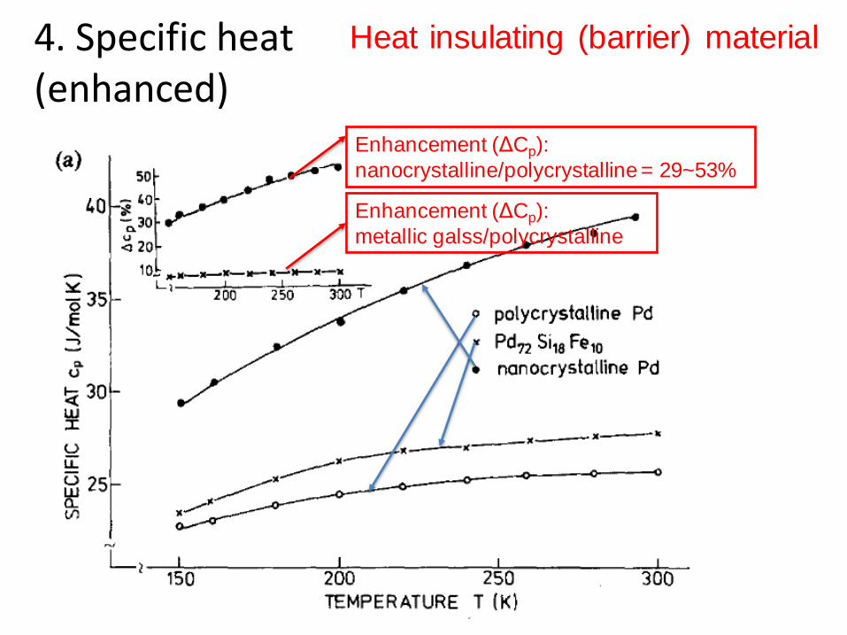
4. Specific heat (enhanced)
Enhancement (ΔCp):
nanocrystalline/polycrystalline = 29~53%
Enhancement (ΔCp):
metallic galss/polycrystalline
Heat insulating (barrier) material
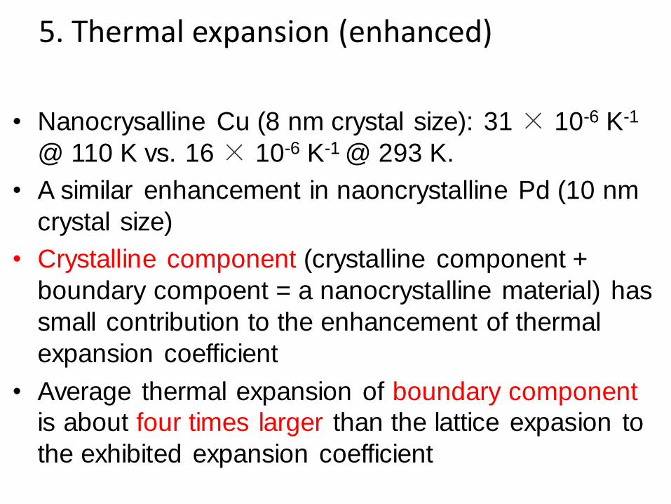
5. Thermal expansion (enhanced)
• Nanocrysalline Cu (8 nm crystal size): 31 × 10-6 K-1
@ 110 K vs. 16 × 10-6 K-1 @ 293 K.
• A similar enhancement in naoncrystalline Pd (10 nm
crystal size)
• Crystalline component (crystalline component +
boundary compoent = a nanocrystalline material) has
small contribution to the enhancement of thermal
expansion coefficient
• Average thermal expansion of boundary component
is about four times larger than the lattice expasion to
the exhibited expansion coefficient
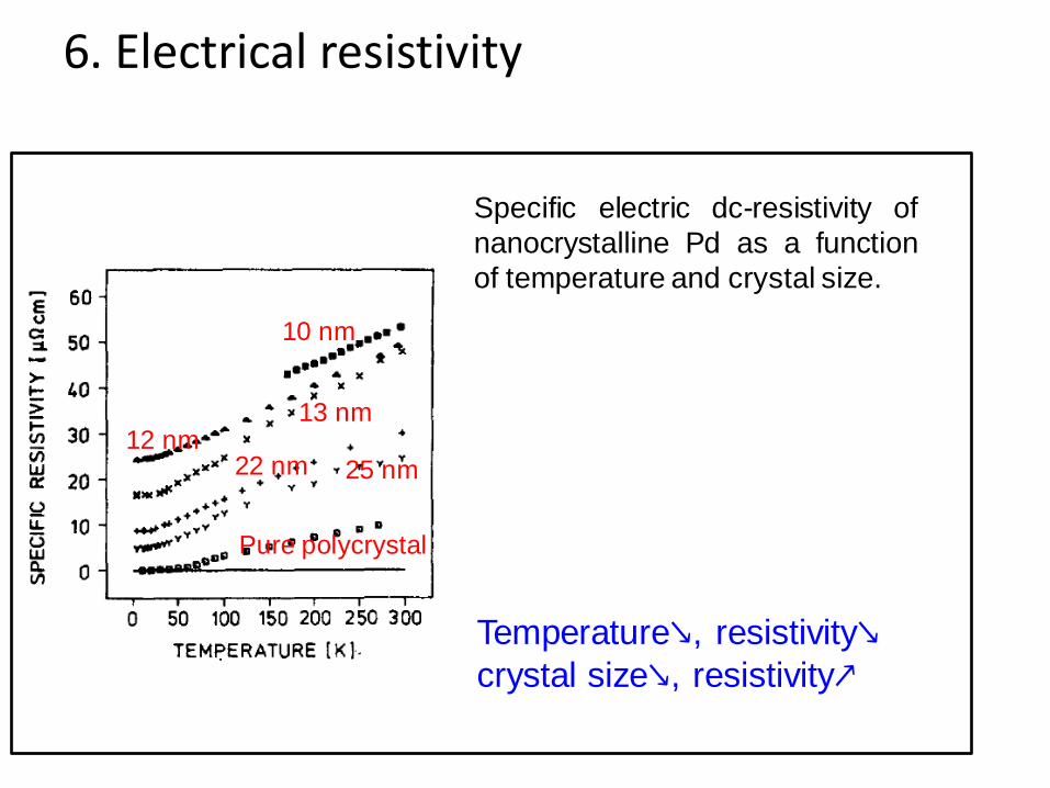
6. Electrical resistivity
Specific electric dc-resistivity of
nanocrystalline Pd as a function
of temperature and crystal size.
10 nm
12 nm 13 nm
22 nm 25 nm
Pure polycrystal
Temperature↘, resistivity↘
crystal size↘, resistivity↗
• The observed trend can be understood in terms of electron scattering inside crystallites and by boundaries.
• The scattering may either be described in terms of the reflection of electrons by boundaries or the transmission through the boundaries.
• If the crystal size is smaller than the electron mean free path, grain boundary scattering dominates and hence the conductivity decrease.
• If the crystal size is larger than the electron mean free path, electron scattering by scattering effects inside of crystal becomes the dominant scattering mode.
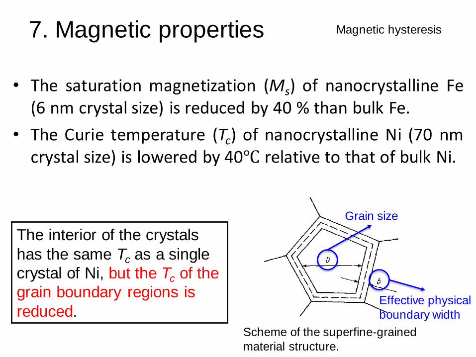
7. Magnetic properties
• The saturation magnetization (Ms) of nanocrystalline Fe (6 nm crystal size) is reduced by 40 % than bulk Fe.
• The Curie temperature (Tc) of nanocrystalline Ni (70 nm crystal size) is lowered by 40℃ relative to that of bulk Ni.
The interior of the crystals
has the same Tc as a single
crystal of Ni, but the Tc of the
grain boundary regions is
reduced.
Scheme of the superfine-grained
material structure.
Grain size
Effective physical
boundary width
Magnetic hysteresis
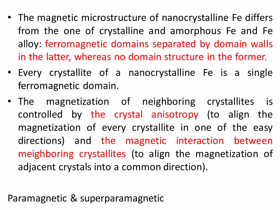
• The magnetic microstructure of nanocrystalline Fe differs from the one of crystalline and amorphous Fe and Fe alloy: ferromagnetic domains separated by domain walls in the latter, whereas no domain structure in the former.
• Every crystallite of a nanocrystalline Fe is a single ferromagnetic domain.
• The magnetization of neighboring crystallites is controlled by the crystal anisotropy (to align the magnetization of every crystallite in one of the easy directions) and the magnetic interaction between meighboring crystallites (to align the magnetization of adjacent crystals into a common direction).
Paramagnetic & superparamagnetic
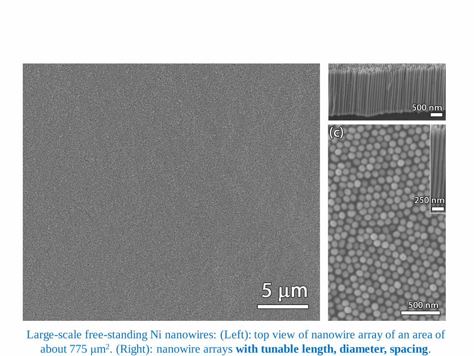
Large-scale free-standing Ni nanowires: (Left): top view of nanowire array of an area of
about 775 μm2. (Right): nanowire arrays with tunable length, diameter, spacing.
Winkler N., Leuthold J., Lei Y., Wilde G., J. Mat.
Chem., 22, 16627, 2012.
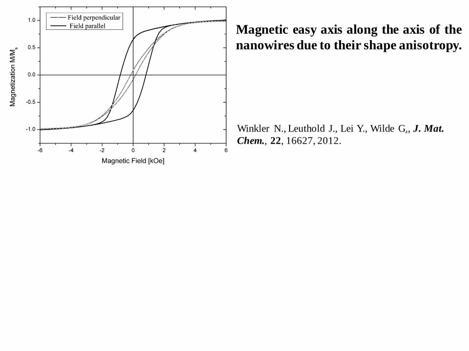
Magnetic easy axis along the axis of the
nanowires due to their shape anisotropy.
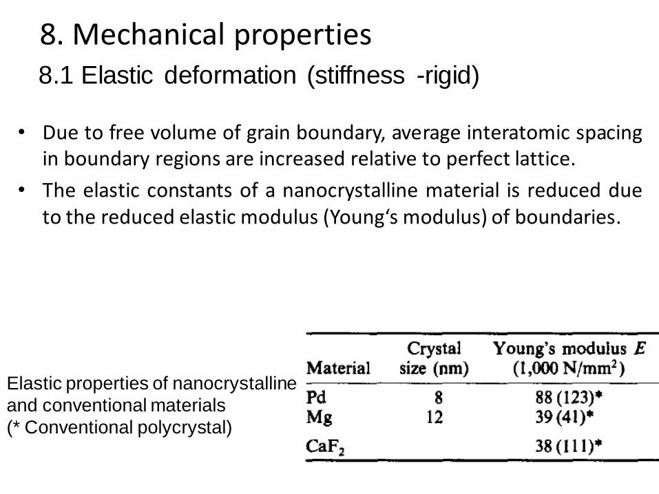
8. Mechanical properties
• Due to free volume of grain boundary, average interatomic spacing in boundary regions are increased relative to perfect lattice.
• The elastic constants of a nanocrystalline material is reduced due to the reduced elastic modulus (Young‘s modulus) of boundaries.
8.1 Elastic deformation (stiffness -rigid)
Elastic properties of nanocrystalline
and conventional materials
(* Conventional polycrystal)
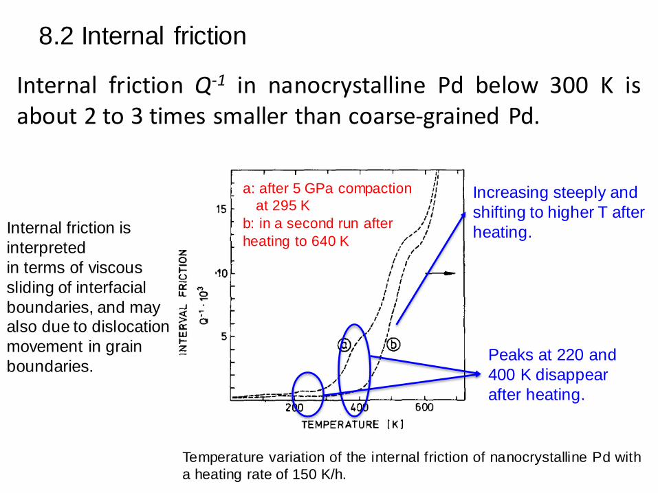
Internal friction Q-1 in nanocrystalline Pd below 300 K is about 2 to 3 times smaller than coarse-grained Pd.
8.2 Internal friction
Temperature variation of the internal friction of nanocrystalline Pd with
a heating rate of 150 K/h.
a: after 5 GPa compaction
at 295 K
b: in a second run after
heating to 640 K
Peaks at 220 and
400 K disappear
after heating.
Increasing steeply and
shifting to higher T after
heating. Internal friction is
interpreted
in terms of viscous
sliding of interfacial
boundaries, and may also due to dislocation
movement in grain
boundaries.
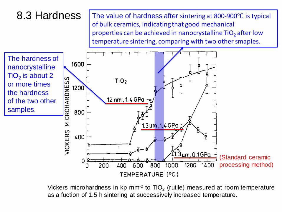
8.3 Hardness
Vickers microhardness in kp mm-2 to TiO2 (rutile) measured at room temperature
as a fuction of 1.5 h sintering at successively increased temperature.
The hardness of
nanocrystalline
TiO2 is about 2
or more times
the hardness of the two other
samples.
(Standard ceramic
processing method)
The value of hardness after sintering at 800-900℃ is typical of bulk ceramics, indicating that good mechanical properties can be achieved in nanocrystalline TiO2 after low temperature sintering, comparing with two other smaples.
8.4 Plastic deformation
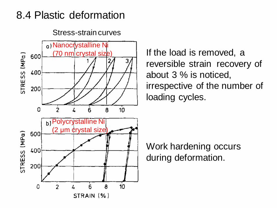
Stress-strain curves
Nanocrystalline Ni
(70 nm crystal size)
Polycrystalline Ni
(2 μm crystal size)
If the load is removed, a
reversible strain recovery of
about 3 % is noticed,
irrespective of the number of
loading cycles.
Work hardening occurs
during deformation.
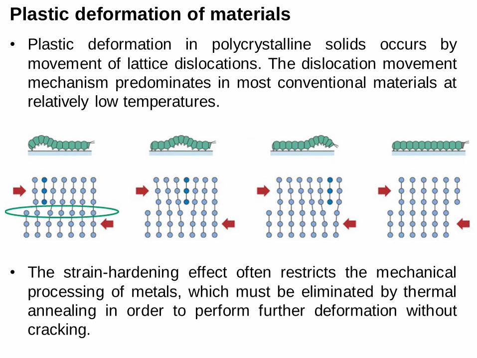
• Plastic deformation in polycrystalline solids occurs by
movement of lattice dislocations. The dislocation movement
mechanism predominates in most conventional materials at
relatively low temperatures.
Plastic deformation of materials
• The strain-hardening effect often restricts the mechanical
processing of metals, which must be eliminated by thermal
annealing in order to perform further deformation without
cracking.
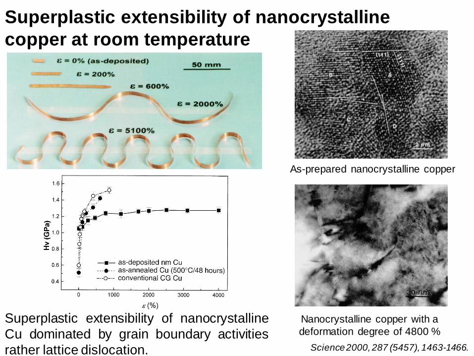
Superplastic extensibility of nanocrystalline
copper at room temperature
As-prepared nanocrystalline copper
Nanocrystalline copper with a
deformation degree of 4800 %
Science 2000, 287 (5457), 1463-1466.
Superplastic extensibility of nanocrystalline
Cu dominated by grain boundary activities
rather lattice dislocation.
Classical methods for strengthening materials
Science 2009, 324 (5925), 349-352.
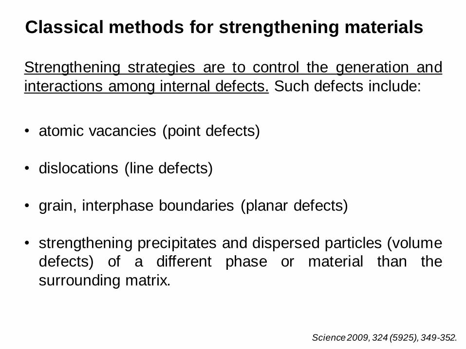
Strengthening strategies are to control the generation and
interactions among internal defects. Such defects include:
• atomic vacancies (point defects)
• dislocations (line defects)
• grain, interphase boundaries (planar defects)
• strengthening precipitates and dispersed particles (volume
defects) of a different phase or material than the
surrounding matrix.
Classical methods for strengthening materials
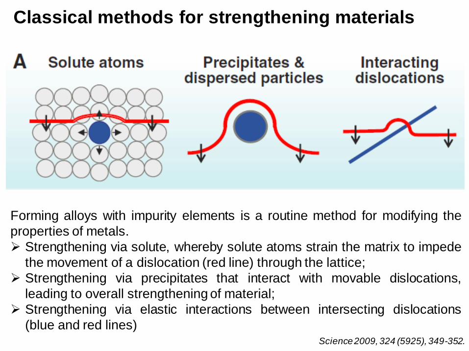
Forming alloys with impurity elements is a routine method for modifying the
properties of metals.
Strengthening via solute, whereby solute atoms strain the matrix to impede
the movement of a dislocation (red line) through the lattice;
Strengthening via precipitates that interact with movable dislocations,
leading to overall strengthening of material;
Strengthening via elastic interactions between intersecting dislocations
(blue and red lines) Science 2009, 324 (5925), 349-352.
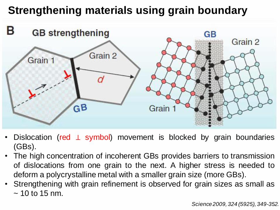
Strengthening materials using grain boundary
Science 2009, 324 (5925), 349-352.
• Dislocation (red ⊥ symbol) movement is blocked by grain boundaries
(GBs).
• The high concentration of incoherent GBs provides barriers to transmission
of dislocations from one grain to the next. A higher stress is needed to
deform a polycrystalline metal with a smaller grain size (more GBs).
• Strengthening with grain refinement is observed for grain sizes as small as
~ 10 to 15 nm.
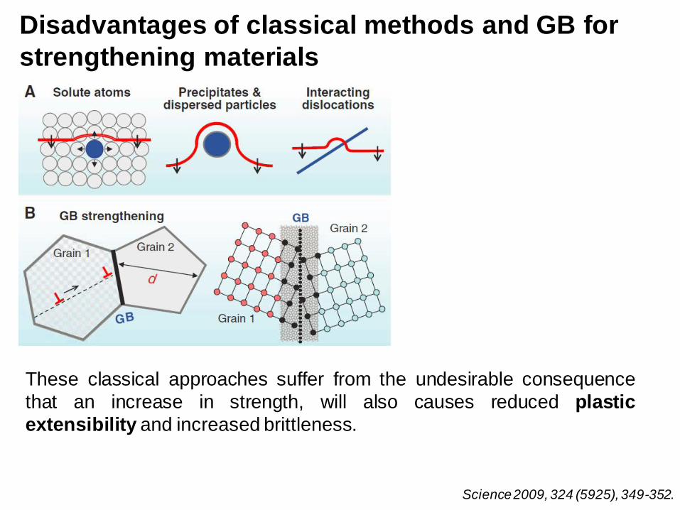
Disadvantages of classical methods and GB for
strengthening materials
Science 2009, 324 (5925), 349-352.
These classical approaches suffer from the undesirable consequence
that an increase in strength, will also causes reduced plastic
extensibility and increased brittleness.
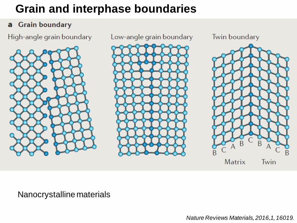
Grain and interphase boundaries
Nature Reviews Materials, 2016,1, 16019.
Nanocrystalline materials
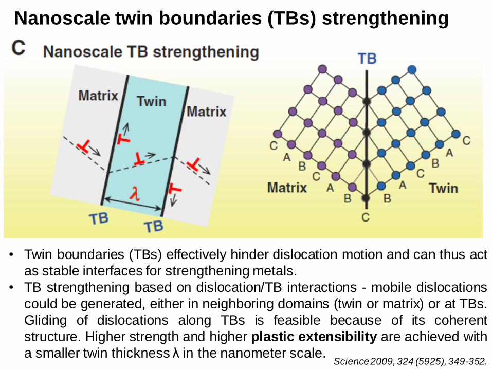
Nanoscale twin boundaries (TBs) strengthening
• Twin boundaries (TBs) effectively hinder dislocation motion and can thus act
as stable interfaces for strengthening metals.
• TB strengthening based on dislocation/TB interactions - mobile dislocations
could be generated, either in neighboring domains (twin or matrix) or at TBs.
Gliding of dislocations along TBs is feasible because of its coherent
structure. Higher strength and higher plastic extensibility are achieved with
a smaller twin thickness λ in the nanometer scale. Science 2009, 324 (5925), 349-352.
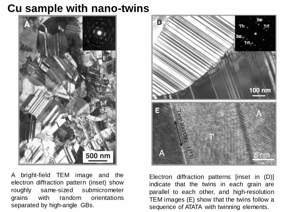
A bright-field TEM image and the
electron diffraction pattern (inset) show
roughly same-sized submicrometer
grains with random orientations
separated by high-angle GBs.
Electron diffraction patterns [inset in (D)]
indicate that the twins in each grain are
parallel to each other, and high-resolution
TEM images (E) show that the twins follow a
sequence of ATATA with twinning elements.
Cu sample with nano-twins
Science 2004, 304 (5669), 422-426.
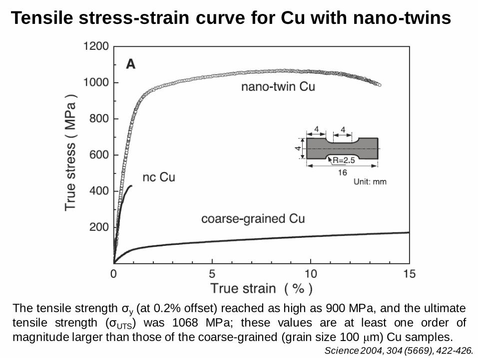
Tensile stress-strain curve for Cu with nano-twins
The tensile strength σy (at 0.2% offset) reached as high as 900 MPa, and the ultimate
tensile strength (σUTS) was 1068 MPa; these values are at least one order of
magnitude larger than those of the coarse-grained (grain size 100 μm) Cu samples.
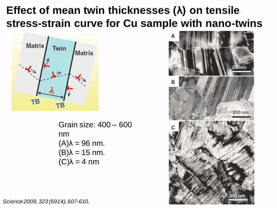
Effect of mean twin thicknesses (λ) on tensile
stress-strain curve for Cu sample with nano-twins
Grain size: 400 – 600
nm
(A)λ = 96 nm.
(B)λ = 15 nm.
(C)λ = 4 nm
Science 2009, 323 (5914), 607-610.
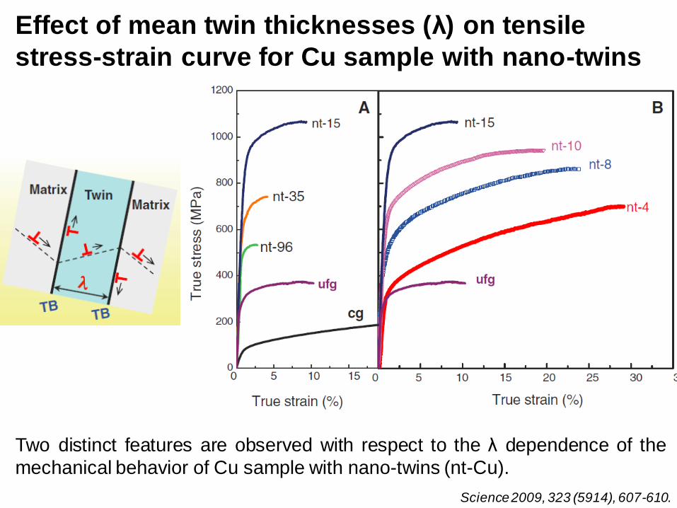
Effect of mean twin thicknesses (λ) on tensile
stress-strain curve for Cu sample with nano-twins
Two distinct features are observed with respect to the λ dependence of the
mechanical behavior of Cu sample with nano-twins (nt-Cu).
Science 2009, 323 (5914), 607-610.
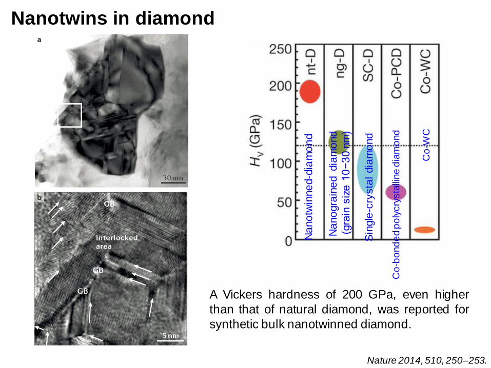
Nanotwins in diamond
A Vickers hardness of 200 GPa, even higher
than that of natural diamond, was reported for
synthetic bulk nanotwinned diamond.
Nature 2014, 510, 250–253.
Na
no
twin
ne
d-d
iam
on
d
Na
no
gra
ine
d dia
mo
nd
(gra
in s
ize
10
−3
0 n
m)
Sin
gle
-cry
sta
l dia
mo
nd
Co
-bo
nd
ed p
oly
cry
sta
lline
dia
mo
nd
Co
-WC
Zentralbau des Deutschen Museums
https://de.wikipedia.org/wiki/Deutsches_Museum
Deutsches Museum
• Class 1: A general introduction of fundamentals of nano-structured materials
• Class 2: Structures and properties of nanocrystalline materials
• Class 3: Graphene
• Class 4: 2D atomically thin nanosheets
• Class 5: Optical properties of 1D nanostructures and nano-generator
• Class 6: Carbon nanotubes
• Class 7: Solar water splitting I: fundamentals
• Class 8: Solar water splitting II: nanostructures for water splitting
• Class 9: Lithium-ion batteries: Si nanostructures
• Class 10: Sodium-ion batteries and other ion batteries, and Supercapacitors
• Class 11: Solar cells
• Class 12: Other nanostructures

Thanks for your attention