Embed Size (px)
Citation preview
出國報告(出國類別:實習)
「新增松山機場 VOR/DME 設備採購案」工廠訓練
服務機關:民用航空局飛航服務總臺
姓名職稱:蔡上田 (工務員)
黃昱瑞 (工務員)
派赴國家:美國堪薩斯
出國期間:103/5/24~103/6/13
報告日期:103/7/28
1
目目目目錄錄錄錄
壹壹壹壹、、、、 目的目的目的目的 ...................................................................................................................... 3
貳貳貳貳、、、、 過程過程過程過程 ...................................................................................................................... 4
參參參參、、、、 內容內容內容內容 ...................................................................................................................... 5
VOR ........................................................................................................................ 5
一、VOR 描述 ...................................................................................................... 5
二、工作原理 ...................................................................................................... 8
三、DVOR 天線的原理 ................................................................................... 18
四、1150 A Doppler VHF Omnirange (DVOR) ................................................... 19
五.、Table 4-1 Standards and Tolerances ............................................................. 45
六、PERFORMANCE CHECK PROCEDURES ................................................. 47
七、Syntersizer CCA 之 Carrier PLL Control 及 Carrier-Sideband Phase Offset 之
設定 ............................................................................................................. 75
八、Sideband Phase Offset 設定 ........................................................................ 82
九、飛測調整 .................................................................................................... 84
十、sideband antenna 之調諧方法 .................................................................... 87
十一、Physical makeup of the alfor loop antenna ................................................ 91
十二、軟體之 update 方法 ............................................................................... 93
DME ...................................................................................................................... 98
一、DME 概述 ................................................................................................... 98
二、模組介紹 .................................................................................................. 100
1. 本地控制單元(Local Control Unit,LCU) ........................................... 102
2. 低功率放大器(Low Power Amplifier,LPA) ....................................... 105
3. 接收/發射控制器(Receiver/Transmitter Controller,RTC) ................... 107
4. 監視器(Monitor) ................................................................................... 107
5. 遠端監控系統(Remote Monitoring System,RMS) .............................. 109
6. Facilities 模組 ........................................................................................ 110

2
7. 界面(Interface)模組 .............................................................................. 111
三、信號傳遞流程 .......................................................................................... 111
1. 詢問波與答詢波 .................................................................................. 111
2. DME 系統自我測試 .............................................................................. 112
四、PMDT ........................................................................................................ 113
1. PMDT 操作 ............................................................................................ 113
2. 回波(Echo)干擾 .................................................................................... 122
肆肆肆肆、、、、 心得與建議心得與建議心得與建議心得與建議 ...................................................................................................... 125
3
壹壹壹壹、、、、 目的目的目的目的
臺北松山機場位於臺北市松山區內,其周遭多為建築物及天然山脈等障礙物
所環繞,為確保航機安全,進場航機不得以目視方式進場。然而該機場 10 跑道
ILS/DME 進場程序,除了以使用 GPS 作為備援程序外,目前尚無其他儀器備援程
序。爰此,為提供跑道另一備援程序,本次採購案新增設松山機場 VOR/DME 設
備乙套,並於民國 103 年完成架設,以促進航機飛行安全,提升飛航服務品質。
本採購案依合約規定,由本總臺派遣航電維護人員參加工廠訓練,並由得標
廠商(設備製造原廠 SELEX Systems Integration)依規定執行訓練課程;本次訓練目的
為藉由原廠教官親自授課,以及學員親自操作原廠訓練用設備,使本總臺受訓同
仁能接受第一手資訊,正確了解設備原理、各機組件的功能,更能在原廠經驗傳
授與親自操作設備的過程中,充份學習如何故障排除,藉此提升參訓學員的技
能。同仁完訓後並可將這份寶貴的經驗與知識帶回本總臺,與未參與原廠受訓的
航電維護同仁分享、傳承,共同為提升航電人員維護設備的技術努力,更為我國
飛航服務奉獻一份心力。
4
貳貳貳貳、、、、 過程過程過程過程
一、參與人員:
蔡上田 民用航空局飛航服務總臺
高雄裝修區臺馬公助航臺工務員
黃昱瑞 民用航空局飛航服務總臺
航電技術室工務員
二、日期:民國 103 年 05 月 24 日至民國 103 年 06 月 13 日。
三、行程:
103.年 05 月 24 日:去程搭乘長榮航空班機,由桃園國際機場飛抵美國洛杉磯
國際機場,再轉搭美國航空班機分別前往芝加哥歐海爾
機場。
103 年 05 月 25 日:由芝加哥奧海爾機場轉機至堪薩斯國際機場。
103 年 05 月 26 日~ 103 年 06 月 11 日:於 SELEX 訓練中心進行為期 17 天之
VOR/DME 設備訓練。
103 年 06 月 11 日:搭乘美國航空班機,由美國堪薩斯國際機場起飛經丹佛機
場抵達洛杉磯國際機場。
103 年 06 月 12 日:回程由洛杉磯國際機場轉機搭乘長榮航空班機返抵桃園國
際機場。
5
參參參參、、、、 內容內容內容內容
VORVORVORVOR
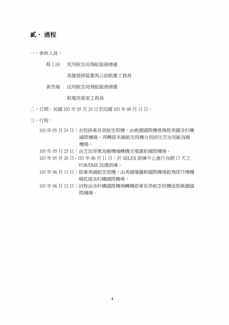
一一一一、、、、VOR 描述描述描述描述
VOR 提供航機以磁北為參考點的方位資料,航機駕駛員依據座艙儀表的指示器指
示,循已選定之輻向飛航,飛向(TO)或背向(From) VOR,就可以達成航路的指向
或是航機終端進場的指向。
VOR 分為 CVOR(Conventional VOR),及 DVOR (Doppler VOR),因 CVOR 容易受
電臺附近大型障礙物干擾的影響使場型失真,因此 CVOR 已漸被 DVOR 所取代。
VOR 的頻帶為 108 ~ 118 MHZ,並經由兩個 30 HZ 的信號作調變,一個是振福調變
另一個是頻率調變(也可以分別稱之為參考相位信號和可變相位信號),環繞 DVOR
站台不同的磁方位有不同的 30 Hz 的相位差,使得航機的方位可以被判定。
當航機由南方朝向 VOR 站台進場時,其圖示如下;
6
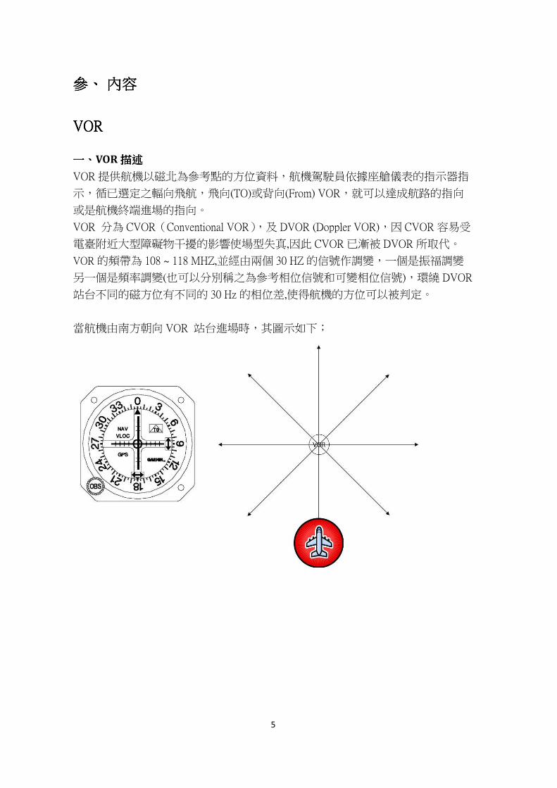
當航機位於 VOR 站台左邊時,座艙儀的表指示器指針會移到右邊,告知駕駛員
須往右邊飛,其圖示如下:
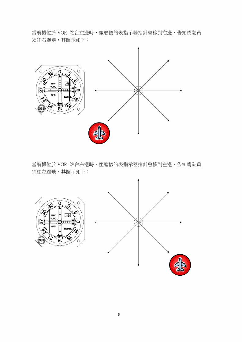
當航機位於 VOR 站台右邊時,座艙儀的表指示器指針會移到左邊,告知駕駛員
須往左邊飛,其圖示如下:
7
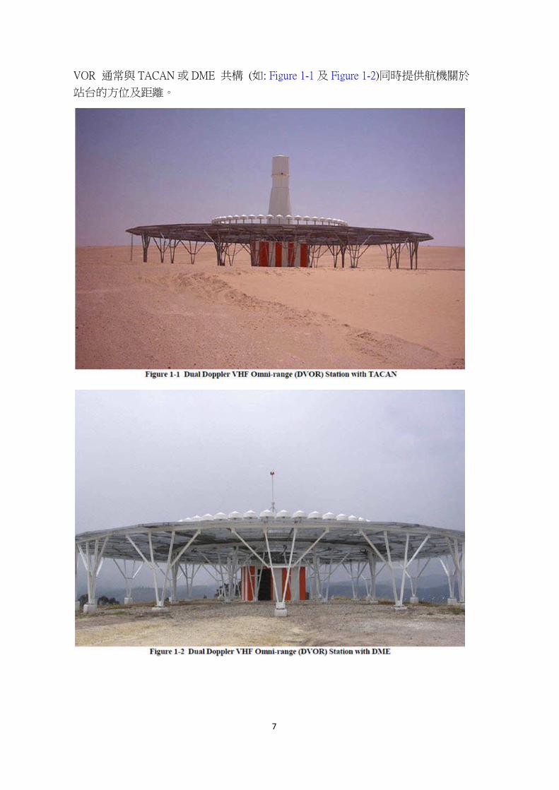
VOR 通常與 TACAN 或 DME 共構 (如: Figure 1-1 及 Figure 1-2)同時提供航機關於
站台的方位及距離。
8
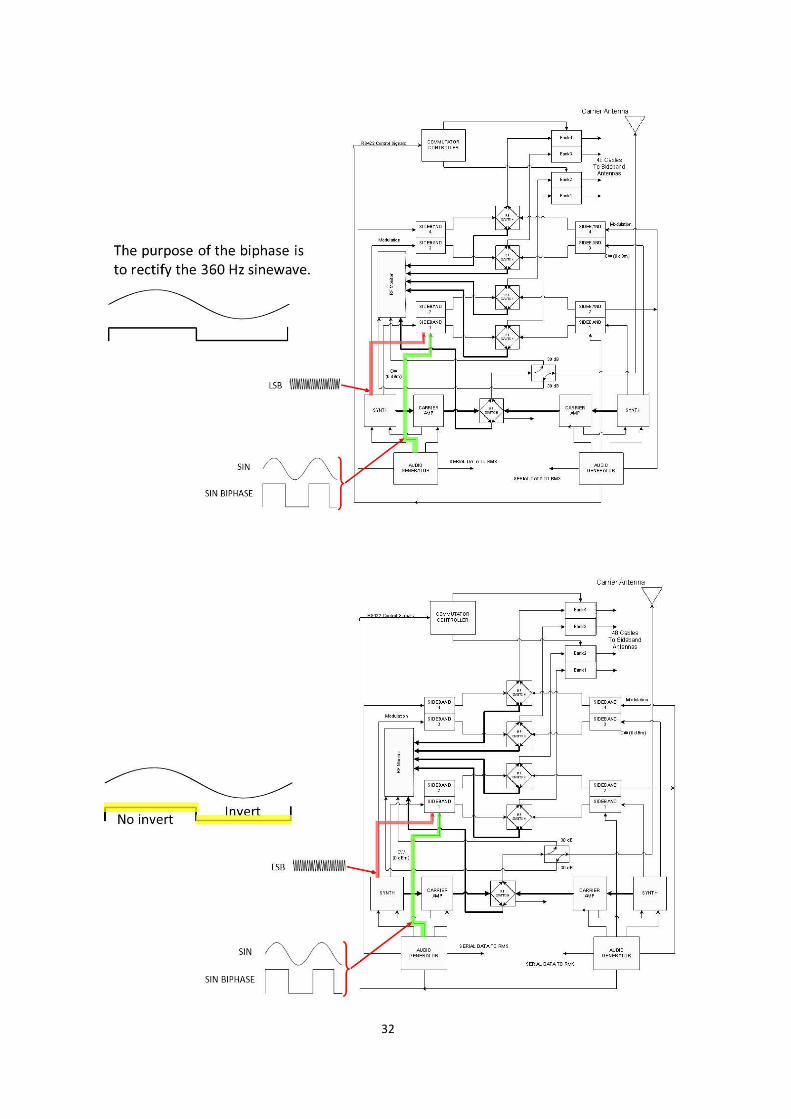
二二二二、、、、工工工工作原理作原理作原理作原理
DVOR 的操作乃根據調變在載波(carrier)的兩個 30 HZ 的信號,其彼此間的相位差
異,被稱之為參考相位和可變相位。
參考的相位信號是經由一個以 30 HZ 正弦波信號的振幅調變載波而獲得,這個振
幅調變(AM)信號是藉由中心的 carrier 天線來發射一個水平面全方向性的信號,這
個輻射的場型是一個圓形的場型,在航機的接收機產生一個在方位具有相位獨立
的 30 HZ 信號。
NOTE
DVOR 必須分別輻射 upper sideband 和 lower sideband 的頻率,他們從 carrier 頻率偏
移± 9960 HZ, 1150A DVOR 具有合成器(synthesizer)控制頻率,它們的設計如下:站
台的頻率加 9960 HZ 以及站台的頻率減 9960 HZ。
可變相位信號可從這個被頻率調變的 9960 HZ 副載波而獲得,(而這副載波再以振
幅調變的方式去調變 carrier 載波,這種 carrier 的振幅調變方式通常被稱之為空中
調變),因為他是藉由 sideband 天線所分別發射的 upper 及 lower 的 sideband 信號添
加在 carrier 所幅射在空中的全方向性信號所獲得的調變信號。
Upper 和 lower 的 sideband 信號分別在 carrier 頻率的上面及下面平均位移 9960 Hz,
並且當添加到載波的相位正確時將產生一個合成的信號,而這信號是被調變在
9960 Hz 的振幅調變。
副載波的頻率調變是以 30 Hz 的速率來作頻率調變,sideband 信號是被順序地分配
到 48 根 sideband 天線,並從這 48 根天線幅射出去,以這樣的方式來模擬兩個徑
向相對的天線,在 sideband 天線的圓周以每秒 30 轉的逆時針旋轉,有一根天線發
射 upper sideband signal,另一根則發射 lower sideband signal。
從 rotating sideband sources 和遠方定點之間的移動路徑的有效長度,在 30 赫茲的速
率變化,觀察到的 sideband 信號的頻率變化也是在 30 Hz 的速率,因此該副載波
是在 30 Hz 的頻率調變。
在航機的接收機,從 9960 Hz 的 FM 副載波取出 30 Hz 的信號,
30 Hz FM 信號的相位與接收點的方位變化呈現線性的變化;
關於每度的方位變化,30 Hz 可變相位信號的相位以一度來做變化,
sideband 天線循序的激能並與 carrier 的 30 Hz 振幅調變的参考相位在同一時間做相
對的比較,在 DVOR 的 0 度磁相時其参考信號和 30 Hz 可變的相位信號是在同相的
(in phase)。
當航機接收的點繞著站台順時針移動時,可變的相位信號(30 HZ FM)開始領先參考
信號( 30 Hz AM ),例如:觀察者在 DVOR 的西邊,30 Hz 的 FM 信號領先 30 Hz
AM 信號 270 度,航機的接收機測得兩個 30 Hz 信號之間的相位差,因而得知到相
對於站台的磁方位,就像是藉由這 30 Hz 的 AM 信號落後 30 Hz 的 FM 信號的度
數。
頻率偏差的量是正比於 sideband 天線圓周的直徑,被表現在工作頻率的波長。
例如:設定 sideband 天線圓周的直徑在 44 呎 (13.4112 公尺)時,其產生 480 HZ
9
的最大頻率偏移是在 113.85 MHz,產生 454 Hz 的最大頻率偏移是在 108 MHz,產
生 497 Hz 的最大頻率偏移是在 118 MHz,因此其相對應的偏差率從 15.13 (在 108
MHz) 到 16.57 (在 118 MHz)。
偏差頻率 (deviation frequency)之計算公式如下:
fd =ν/λ
fd : 偏差頻率 (deviation frequency)
fc : DVOR 頻率
γ: Sideband 天線圓周半徑
ω = 2πf π= 3.14159 f = 30 Hz
ν=γω
λ = DVOR 頻率波長= 光速/ DVOR 頻率
頻率偏差率(deviation rate) = fd /30
例如:
sideband 天線的圓周直徑為 44 呎 (13.4112 公尺),DVOR 頻率為 113.85 MHz,
其偏差頻率其偏差頻率及偏差率之計算如下:
γ: Sideband 天線圓周半徑 =13.4112 m / 2
ω = 2πf π= 3.14159 f = 30 Hz
ν=γω = (13.4 112 m / 2) x 2 x 3.14159 x 30 = 1263.975 m/s
λ = 3x10⁸/(113.85x10
6) = 2.635 m
fd =ν/λ = 1263.975/2.635 = 480 Hz
所以偏差率(deviation rate) = 480/30 = 16
--------------------------------------------------------------------
例如:
sideband 天線的圓周直徑為 44 呎 (13.4112 公尺),DVOR 頻率為 108 MHz,
其偏差頻率及偏差率之計算如下:
fd =ν/λ
γ: Sideband 天線圓周半徑 =13.4112 m / 2
ω = 2πf π= 3.14159 f = 30 Hz
ν=γω = (13.4 112 m / 2) x 2 x 3.14159 x 30 = 1263.975 m/s
λ = 3x10⁸/(108x10
6) = 2.778 m
fd =ν/λ = 1263.975/2.778 = 455 Hz
所以偏差率(deviation rate) = 455/30 = 15.167
例如:
10
sideband 天線的圓周直徑為 44 呎 (13.4112 公尺),DVOR 頻率為 118 MHz,
其偏差頻率及偏差率之計算如下:
fd =ν/λ
γ: Sideband 天線圓周半徑 =13.4112 m / 2
ω = 2πf π= 3.14159 f = 30 Hz
ν=γω = (13.4 112 m / 2) x 2 x 3.14159 x 30 = 1263.975 m/s
λ = 3x10⁸/(108x10
6) = 2.542 m
fd =ν/λ = 1263.975/2.542 = 497 Hz
所以偏差率(deviation rate) = 497/30 = 16.57
--------------------------------------------------------------------
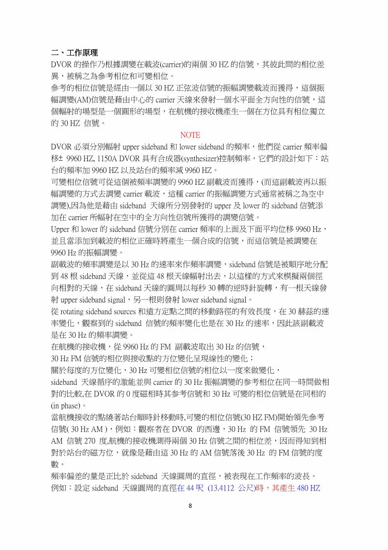
圖 2-1:DVOR 工作在 Fc 的頻率時典型的 DVOR 射頻頻譜。
圖 2-1
11
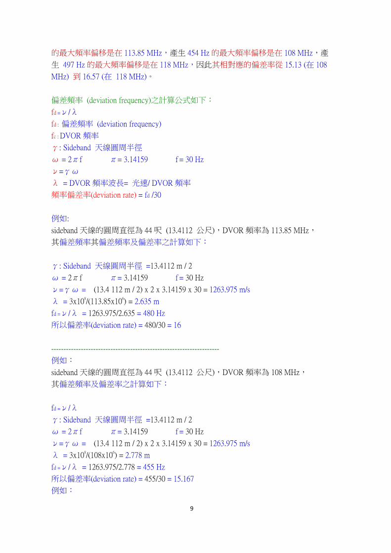
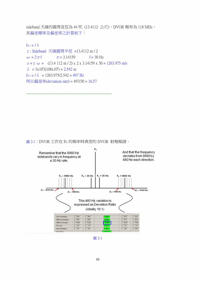
圖 2-2 ~ 2-4:航機接收機在 DVOR 東、西、南、北 等 4 個位置之參考信號(AM)與
可變信號(FM)之相對相位。
圖 2-2 當航機位於 DVOR 之磁北(0 度)方向,AM 與 FM 為同相位
圖 2-3 當航機位於 DVOR 之南方,AM 落後 FM 相位 180 度
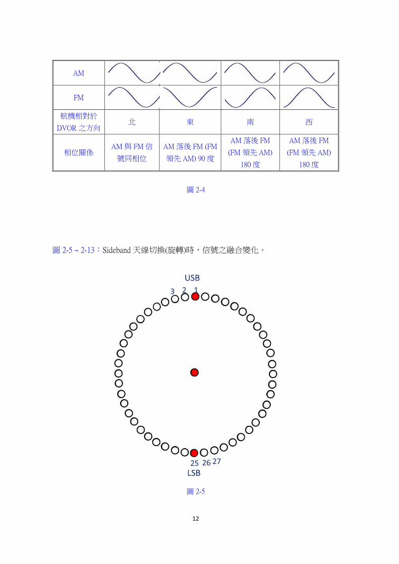
12
AM
FM
航機相對於
DVOR 之方向 北 東 南 西
相位關係 AM 與 FM 信
號同相位
AM 落後 FM (FM
領先 AM) 90 度
AM 落後 FM
(FM 領先 AM)
180 度
AM 落後 FM
(FM 領先 AM)
180 度
圖 2-4
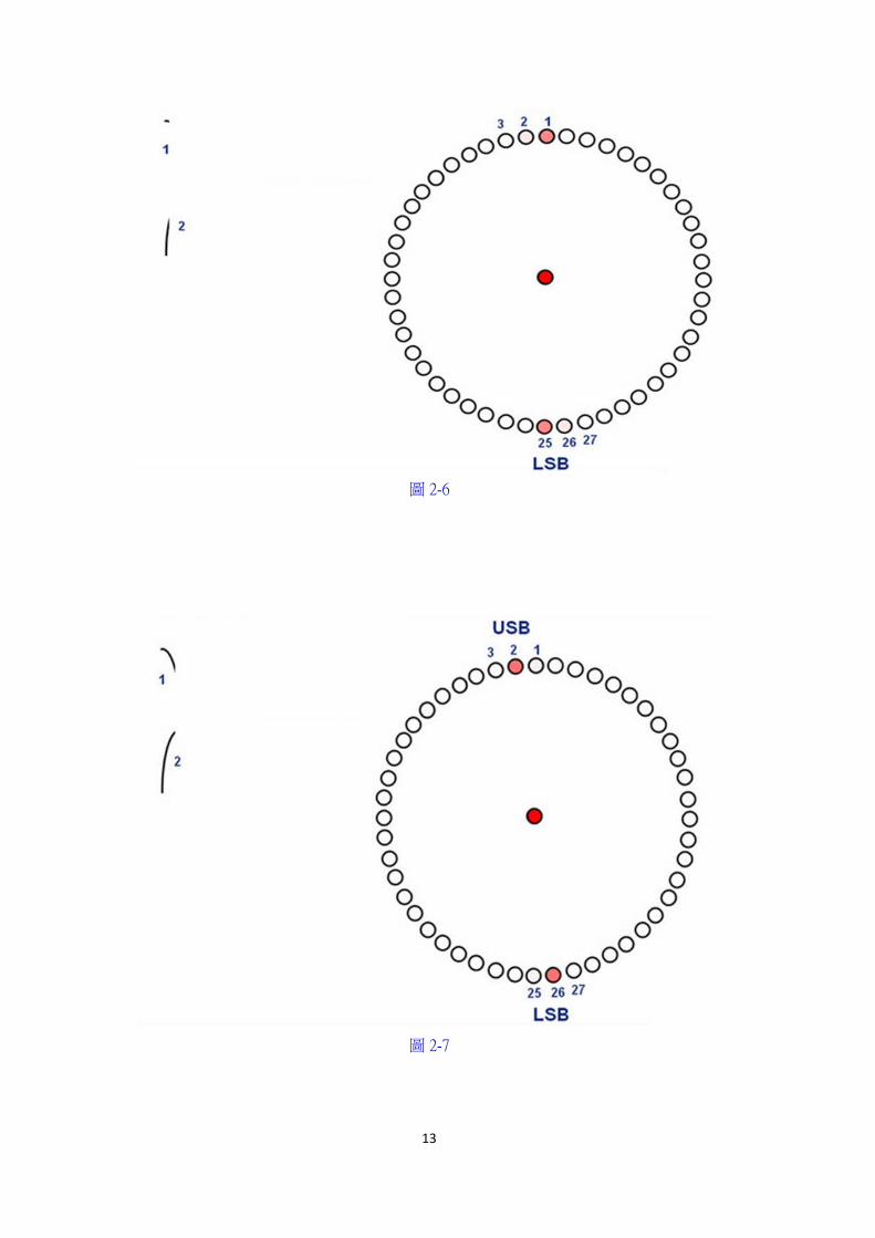
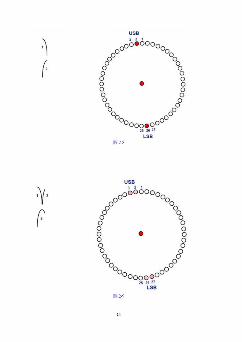
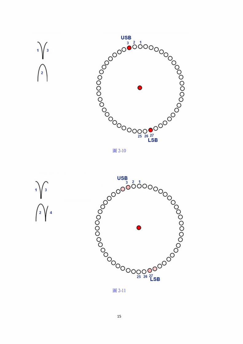
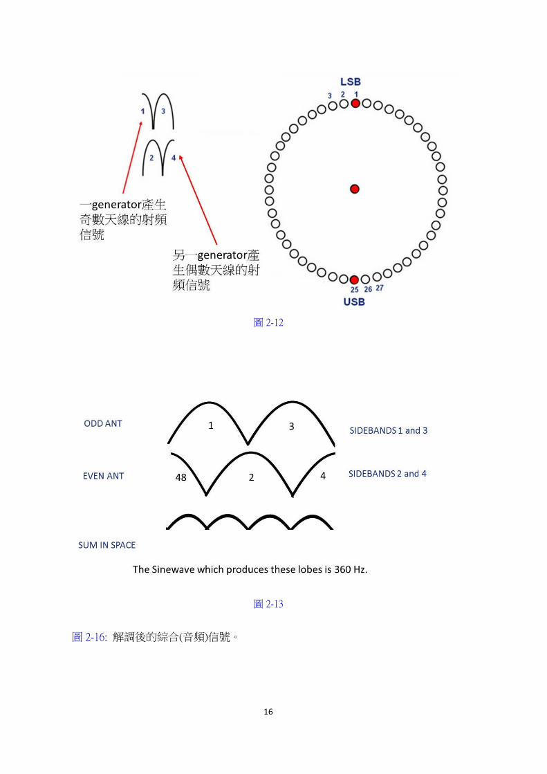
圖 2-5 ~ 2-13:Sideband 天線切換(旋轉)時,信號之融合變化。
圖 2-5
13
圖 2-6
圖 2-7
14
圖 2-8
圖 2-9
15
圖 2-10
圖 2-11
16
圖 2-12
圖 2-13
圖 2-16: 解調後的綜合(音頻)信號。
17
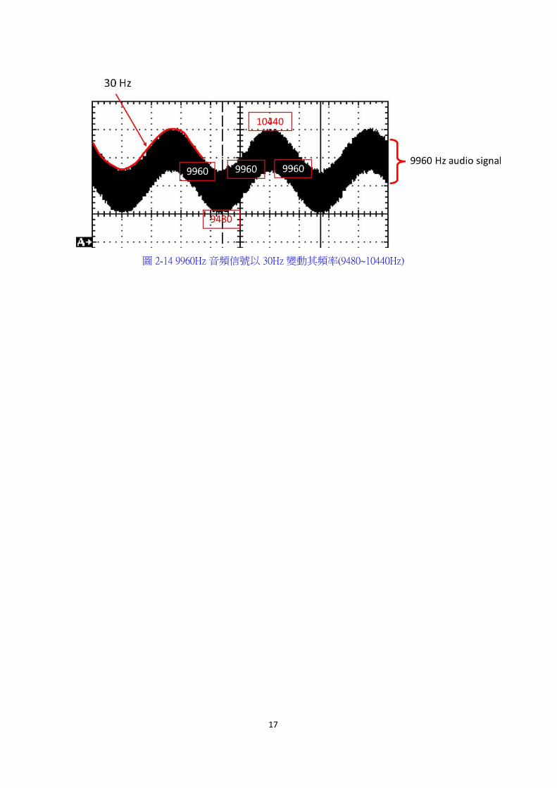
圖 2-14 9960Hz 音頻信號以 30Hz 變動其頻率(9480~10440Hz)
18
三三三三、、、、DVOR DVOR DVOR DVOR 天線的原理天線的原理天線的原理天線的原理
DVOR 系統利用每一根末端的天線模擬成一個旋轉臂,從天線的一端發射 upper
sideband 信號,另一端的天線則發射 lower sideband 信號,
利用直徑為 44 呎(13.4 公尺)在圓周等距離的 48 根 sideband 天線以電子的方法來
達成一個旋轉臂,並在圓心發射一個參考的 carrier 信號(reference carrier)
考慮模擬天線旋轉(simulated antenna rotation)對航機接收機的效應(影響),
當 upper sideband source 朝向航機移動時,因為 Doppler 效應的關係使得進入到航機
接收機的頻率大於 Fc+9960 Hz,而對於 lower sideband source 則是逐漸遠離,頻率
變成低於 Fc-9960 Hz (Fc 是載波頻率 Carrier frequency)
這頻率差異的正弦規律變化是起因於這模擬的旋轉(simulated rotation),最大的頻率
差是發生在兩個發射的天線所連成的直線與徑向的航機發生垂直的時候
,頻率差為零時是發生在兩個 sideband sources 對齊(對準) (來自)徑向的航機,在這
一刻 sideband sources 和航機接收機之間是沒有變化的,
航機環繞在 DVOR 圓周的不同位置時所產生的零頻率偏差是不一樣的,
為此,在這些不同位置所被還原的 30 Hz FM 信號將有一個不同的相位,
航機接收機在 DVOR 北邊的位置,其 30 Hz FM 的信號必須是和 30 HZ AM 信號同
相位;兩個信號同時正好通過(穿過)正零的交叉點。
為了實現這一點,底下必須被遵守: 30 Hz 振幅調變的載波正通過其正零交叉點
的時刻,這被模擬的旋轉(simulated rotating)天線將和 1 號天線及 25 號天線對齊平行
(1 號天線位於磁北,25 號天線位於磁南),用(以)磁北的天線發射 lower sideband 的
峰值信號以及磁南的天線發射 upper sideband 的峰值信號,則 lower sideband 頻率將
減小而 upper sideband 頻率將增加。副載波頻率將正好是由 9960Hz 向上增加以及
30 Hz FM 信號正好通過它的正零交叉點。
19
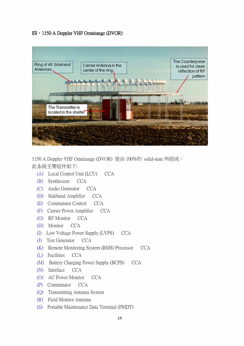
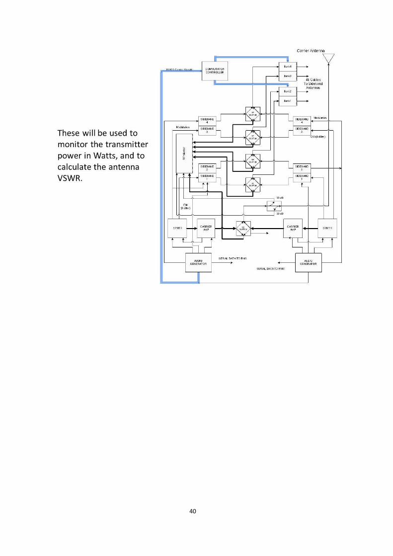
四四四四、、、、1150 A Doppler VHF Omnirange (DVOR)1150 A Doppler VHF Omnirange (DVOR)1150 A Doppler VHF Omnirange (DVOR)1150 A Doppler VHF Omnirange (DVOR)
1150 A Doppler VHF Omnirange (DVOR) 是由 100%的 solid-state 所組成。
此系統主要組件如下:
(A) Local Control Unit (LCU) CCA
(B) Synthesizer CCA
(C) Audio Generator CCA
(D) Sideband Amplifier CCA
(E) Commutator Control CCA
(F) Carrier Power Amplifier CCA
(G) RF Monitor CCA
(H) Monitor CCA
(I) Low Voltage Power Supply (LVPS) CCA
(J) Test Generator CCA
(K) Remote Monitoring System (RMS) Processor CCA
(L) Facilities CCA
(M) Battery Charging Power Supply (BCPS) CCA
(N) Interface CCA
(O) AC Power Monitor CCA
(P) Commutator CCA
(Q) Transmitting Antenna System
(R) Field Monitor Antenna
(S) Portable Maintenance Data Terminal (PMDT)
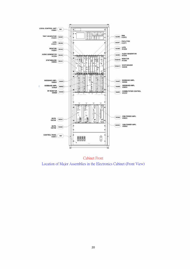
20
Cabinet Front
Location of Major Assemblies in the Electronics Cabinet (Front View)
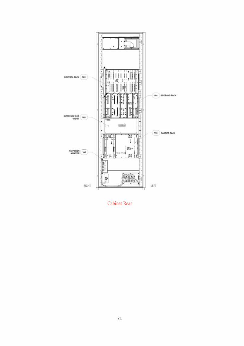
21
Cabinet Rear
22
23
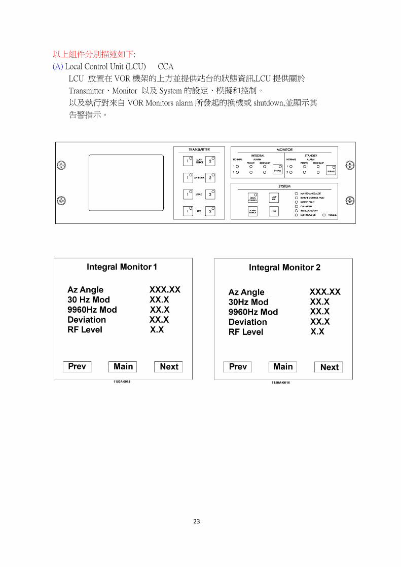
以上組件分別描述如下:
(A) Local Control Unit (LCU) CCA
LCU 放置在 VOR 機架的上方並提供站台的狀態資訊,LCU 提供關於
Transmitter、Monitor 以及 System 的設定、模擬和控制。
以及執行對來自 VOR Monitors alarm 所發起的換機或 shutdown,並顯示其
告警指示。
24
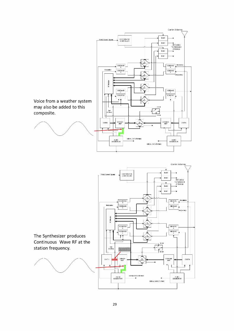
(B) Synthesizer CCA
Synthesizer 產生 Carrier, upper sideband 和 lower sideband 等 3 個 RF
信號給 Transmitter。
有 3 個 board 在 Synthesizer Assembly 內:
1. Carrier board 提供 carrier 頻率和相位控制的能力給 Carrier
Amplifier。
2. Sideband board 產生 upper sideband 和 lower sideband 的頻率給
Sideband Amplifier Assemblies。
3. Interface board 提供連線到背板以及包括到 Audio Generator 和
RMS processors 的數位介面電路。
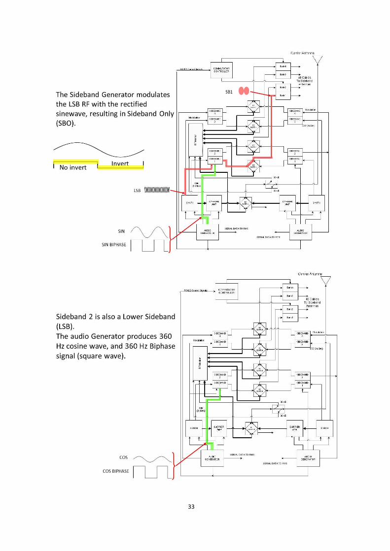
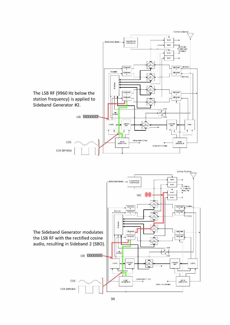
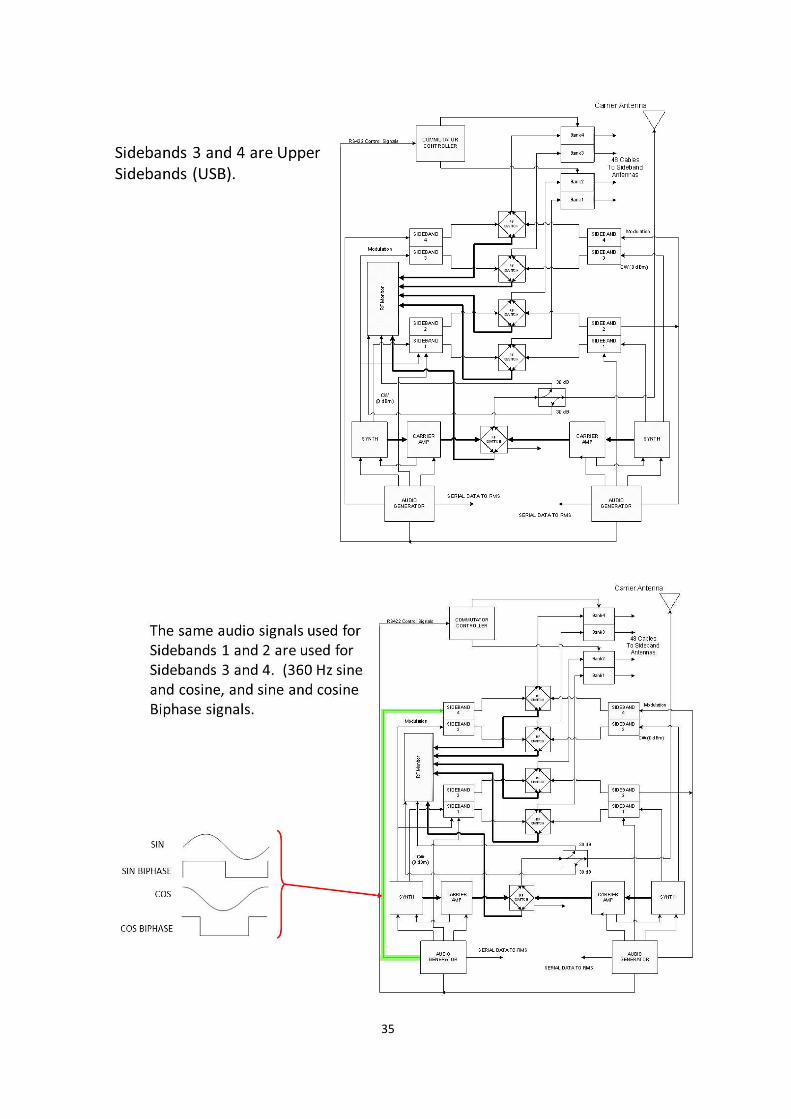
(C) Audio Generator CCA
Audio Generator CCA 提供三個主要輸出:
1. 提供 Commutator 的切換信號
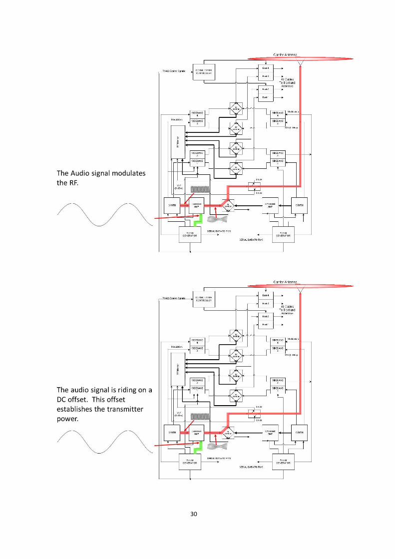
2. 提供 CSB 的 Audio 信號: 30 Hz + 1020 Hz + Voice + DC offset。
註: Audio 信號是騎在 DC offset 上, 這 DC offset 確立了發射功率。
3. 提供 sideband 四個單獨的 Audio Signal。
(D) Sideband Amplifier CCA
Sideband Amplifier Assembly 安裝在 DVOR 機架的 middle rack (1A4),每
個 CH 均有兩塊 Sideband Amplifier 模組,且每一個 Sideband Amplifier
模組均產生兩個分離的 RF 信號,兩個信號都是高於載波頻率 9960 Hz
(upper sideband),或是兩個信號都是低於載波頻率 9960 Hz(lower
sideband)。
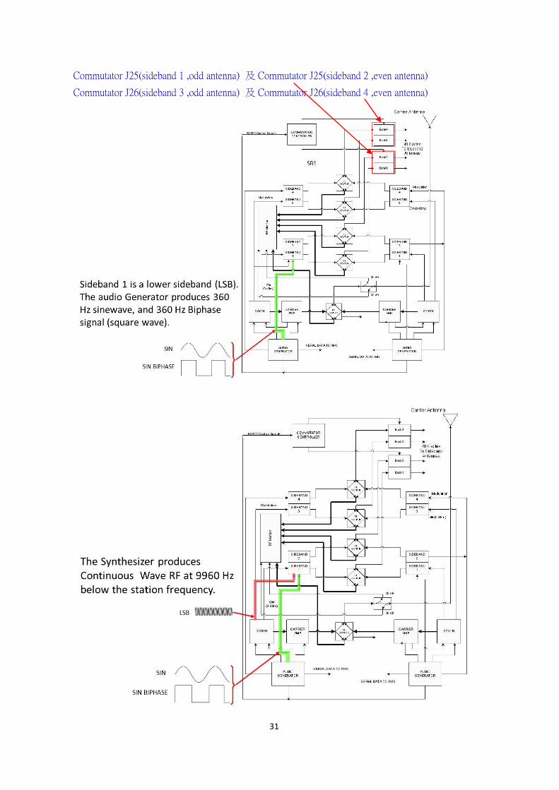
(E) Commutator Control CCA
Commutator Control CCA 連接到在背板 CCA 上一條 25 芯的 cable 上,這
cable 的起源是來自 control rack 內的兩個 Audio Generators 的其中一個。
Commutator Control CCA 出口到背板和到兩個 40 pin 的 connectors,這兩
個 40 pin 的 connectors 連接到來自 Commutator CCAs 的排線(ribbon
cable)。
Commutator Control CCA 處理從 Sideband 1 天線到 Sideband 48 天線的所
有轉向切換信號。
Commutator 的切換控制信號是來自於 Audio Generator CCA。
25
(F) Carrier Power Amplifier CCA
載波放大器有一個組件:載波放大器的電路卡片組件,該組件也是這塊模組
的 I / O,處理來自音頻產生器(Audio Generator)的控制信號,來適當地控制所
需要的輸出 RF 調變和振幅。這組件能夠在最高達 80%的 AM 調變下提供 100
瓦或更高的載波功率。
(G) RF Monitor CCA
RF Monitor Assembly 安裝在 DVOR 機架的 middle rack (1A4),
The RF monitor assembly functions as an RF detector/amplifier and
distributor of the detected RF signals。
為了 carrier power,RF monitor assembly 內有一個 high power 的 dummy
load 並安裝到散熱片上,這散熱片是附著在這組件的 chassis 上,
以及 RF monitor assembly 內有 4 個 sideband dummy load。
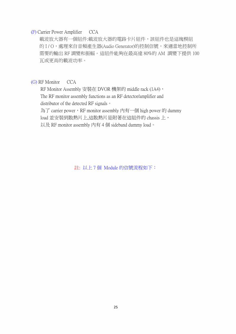
註: 以上 7 個 Module 的信號流程如下:
26
Simplified DVOR Transmitter Block Diagram
27
28
29
30
31
Commutator J25(sideband 1 ,odd antenna) 及 Commutator J25(sideband 2 ,even antenna)
Commutator J26(sideband 3 ,odd antenna) 及 Commutator J26(sideband 4 ,even antenna)
32
33
34
35
36
37
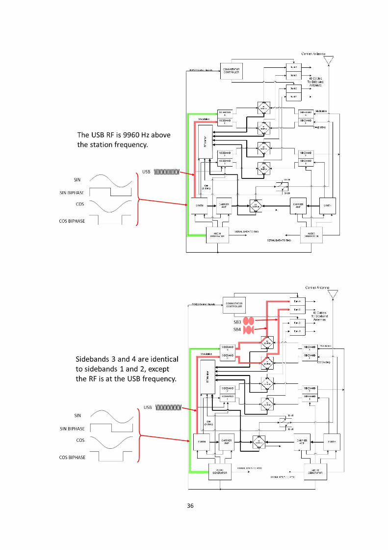
Sideband 1 及 Sideband 2 的振幅相同,頻率相同 (720 Hz)
Sideband 1 (sin Bi-phase)
Sideband 2 (cos Bi-phase)
38
39
40
41
(H) Monitor CCA
Monitor CCA 放大來自 field monitor antenna 的 RF 輸入信號,然後,帶通
濾波和分析這信號,參數化的數據被顯示在 PMDT,並且如果 DVOR 在 limit
的指定範圍內發生 fail 則 Monitor CCA 會發起一個告警狀態指示在 LCU 上。
(I) Low Voltage Power Supply (LVPS) CCA
有兩個 LVPS 的組件被安裝在發射機的機架上,
LVPS 1A3A4 是 1 號發射機的 low voltage power supply
LVPS 1A3A8 是 2 號發射機的 low voltage power supply
每一個 LVPS 在構造和操作上是完全相同的,每一個 LVPS 是可以互換的。
(J) Test Generator CCA
Test Generator CCA 執行兩個功能:
第一個功能:提供一個標準的參考信號給 DVOR 的 monitors 作為校正用,藉由
RMS CPU 來導演模擬完整的測試。
第二個功能:是操作者維護功能,它允許測試信號被送到 monitor(s),藉由操
作者透過 PMDT 來作導演(指示),操作者可以變化不同的參數(比
如:音頻的語音頻帶(voice band audio frequency),百分比調變、
相位偏移等等)來判斷一個 monitor 是否在正常的功能,並且在
要求的設定將發生 alarm。
(K) Remote Monitoring System (RMS) Processor CCA
Remote Monitoring System (RMS) Processor CCA 控制:發射機和模擬系
統(controls transmitter and monitoring systems)。
RMS CCA 藉由 13 個 serial ports 以及 1 個 parallel 來進行通信,
以及方便在單機 VOR 或雙機 VOR 系統作模擬/控制(monitoring/control)。
RMS CCA 接受來自 BCPS 電池供電的 DC power (battery-backed DC power
from BCPS)。
RMS CPU 包含一個 micro controller、RAM、EPROM、EEPROM、bus control
和 Power monitor 電路。RMS CPU 處理系統狀態,指導(引導)和外界的通
信,以及和 DVOR 的 monitor 及 audio generator 之間的通信。
42
(L) Facilities CCA
Facilities CCA 提供系統的 I/O (system I/O)給 RMS CCA。Facilities CCA
的許多輸入和輸出通過 Control Backplane CCA 的路由(路徑)後,最終連
接到 Interface CCA。
System battery –backed power supply (一般是 48 VDC)進入 Facilities
CCA 後,調降為數個不同的低壓;包括:+24 VDC,±15 VDC,±12 VDC,
+5 VDC ,+3.3 VDC。
(M) Battery Charging Power Supply (BCPS) CCA
AC 或 Batteries 的任一個輸入源進入 BCPS 後,再由 BCPC 提供穩定的電壓
給發射機,BCPS 的組件被放置在第 3 個 rack,AC 的輸入電壓進到 BCPS 後
轉換成大約 50 伏特的直流電壓,當 AC 電壓存在時,BCPS 亦負責對
Batteries 充電。
(N) Interface CCA
Interface CCA 提供 RMS/Facilities /Control Backplane CCAs 與外界
間的連接,例如包括:
1. Spare analog and digital inputs
2. Spare digital outputs
3. Temperature sensors
4. Smoke detector
5. Intrusion sensor
等等,RS232 的通信被提供到 RCSU 和 PMDT 以及 Ethernet module。所有
的信號在輸出前藉由暫態電壓抑制器來做保護。
(O) AC Power Monitor CCA
AC Power Monitor CCA 提供一個關於 VOR 系統來測量障礙燈和 VOR 系統
本身的交流電流和電壓的方法。提供結合一個 photo switch 的操作並為
了障礙燈而提供一種功能來 bypass photo witch。
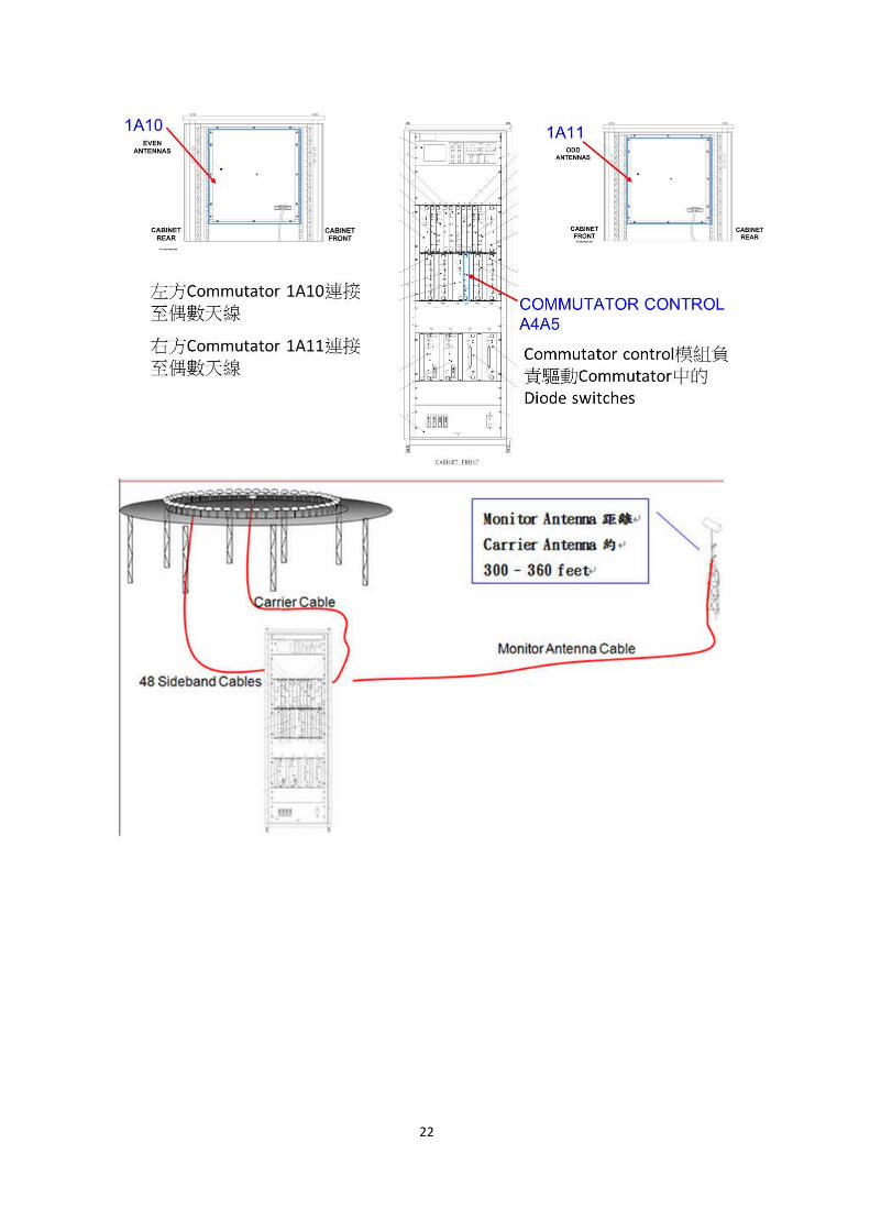
(P) Commutator CCA
有兩個 commutator 安裝在機架的上方,它們被安裝在左上方及右上方的
側邊,經由移除側邊的板子後可以看到這些 commutator,從前面看過去右
側的 commutator 被用來切換 RF 信號到奇數的天線,從前面看過去左側的
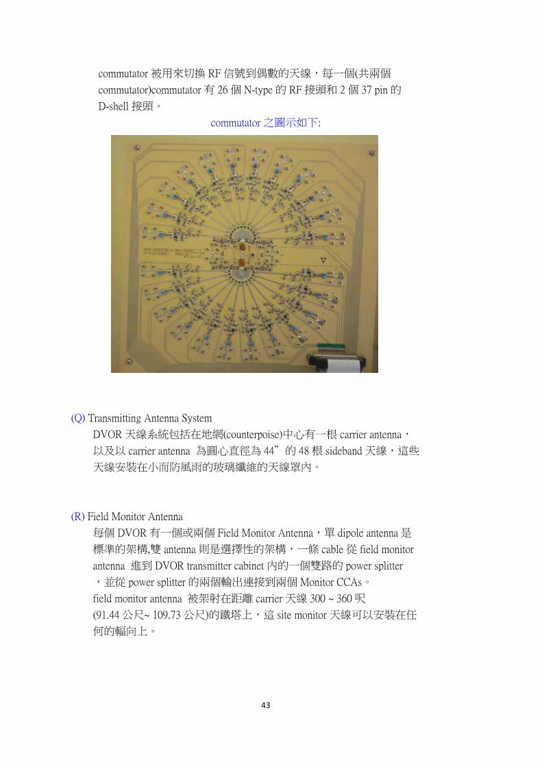
43
commutator 被用來切換 RF 信號到偶數的天線,每一個(共兩個
commutator)commutator 有 26 個 N-type 的 RF 接頭和 2 個 37 pin 的
D-shell 接頭。
commutator 之圖示如下:
(Q) Transmitting Antenna System
DVOR 天線系統包括在地網(counterpoise)中心有一根 carrier antenna,
以及以 carrier antenna 為圓心直徑為 44”的 48 根 sideband 天線,這些
天線安裝在小而防風雨的玻璃纖維的天線罩內。
(R) Field Monitor Antenna
每個 DVOR 有一個或兩個 Field Monitor Antenna,單 dipole antenna 是
標準的架構,雙 antenna 則是選擇性的架構,一條 cable 從 field monitor
antenna 進到 DVOR transmitter cabinet 內的一個雙路的 power splitter
,並從 power splitter 的兩個輸出連接到兩個 Monitor CCAs。
field monitor antenna 被架射在距離 carrier 天線 300 ~ 360 呎
(91.44 公尺~ 109.73 公尺)的鐵塔上,這 site monitor 天線可以安裝在任
何的輻向上。
44
(S) Portable Maintenance Data Terminal (PMDT)
標準的 PMDT 包括一台筆電和輸入/輸出的裝置用來控制及與 DVOR 系統作
通信,系統的控制、調整及 monitoring 的功能可以經由這部電腦的 window
界面來作存取,操作者可利用滑鼠與筆電互相配合,亦可使用桌上型的電
腦取代筆電,印表機亦可與筆電或桌上型電腦相配合。
站臺的安全功能可以經由一個 3-level password system 來提供:
Level 3:可以做系統的調整及測量
Level 2:可以做非關鍵參數的修改
Level 1:可以做系統的讀取
在 Local PMDT 的所有功能可以利用 modem 和撥號的電話線路到遠端另一
臺筆電或桌上型電腦上的 PMDT 上 run。
45
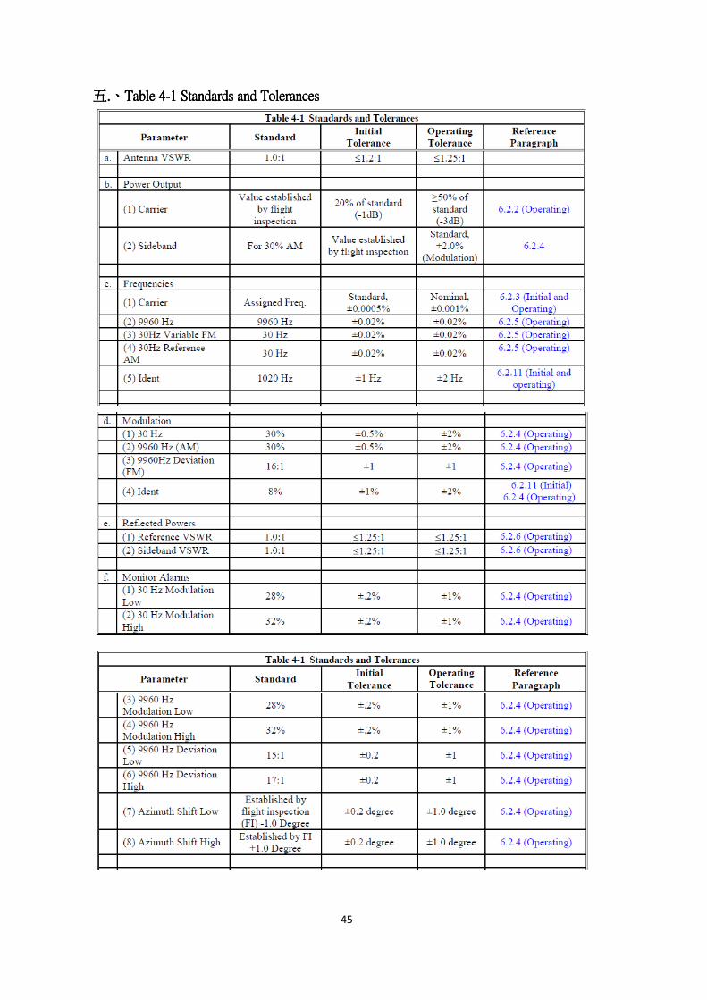
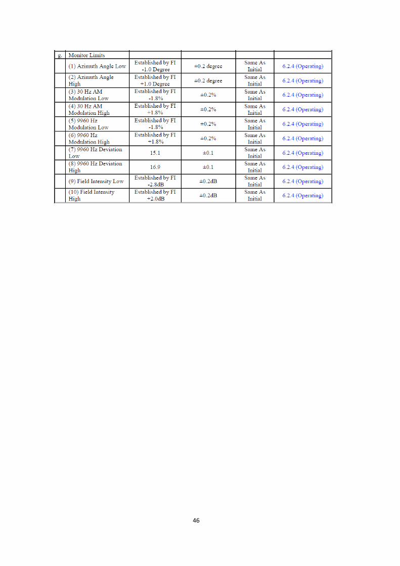
五五五五....、、、、Table 4Table 4Table 4Table 4----1 Standards and Tolerances1 Standards and Tolerances1 Standards and Tolerances1 Standards and Tolerances
46
47
六六六六、、、、PERFORMANCE CHECK PROCEDURESPERFORMANCE CHECK PROCEDURESPERFORMANCE CHECK PROCEDURESPERFORMANCE CHECK PROCEDURES
6. 2 PERFORMANCE CHECK PROCEDURES
Should abnormal performance occur during the performance check procedures, refer to
Section 7.
6.2.1 Battery Backup Transfer Performance Check
a. Logon the PMDT
b. Select RMS >> Status >> VOR Status.
c. With all cabinet circuit breakers in the ON position (AC and DC and Battery),
turn off AC circuit breaker for Transmitter 1. Verify that the VOR system
continues to function and the "Maintenance Alert" status feature
changes to indicate an alert condition.
d. Select RMS >> Data >> Maintenance Alerts/Alarms
e. Verify the "Sys 48 VDC PS 1 Failure" status feature indicates an alert
condition.
f. If the VOR is a dual system, turn off AC circuit breaker for
Transmitter 2. Verify the VOR system continues to function and the
"Sys 48 VDC PS 2 Failure" status feature indicates an alert condition.
g. Restore the system to Normal State
6.2.2 Carrier Output Power Performance Check
a. Logon the PMDT
b. Verify that transmitter 1 is operating.
c. Select Transmitters >> Configuration >> Nominal. Verify Output Power is
the same as commissioning reference.
d. Select Transmitters >> Data >> Transmitter Data. observe that Carrier
Power for transmitter 1 is within the operating tolerance of Table 4-1 (b)(1).
If not in tolerance perform alignment per paragraph 6.4.6
e. For dual system place transmitter 2 on antenna.
f. Select Transmitters >> Data >> Transmitter Data. observe that Carrier
Power for transmitter 2 is within the operating tolerance of Table 4-1 (b)(1).
If not in tolerance perform alignment per paragraph 6.4.6
g. Restore the system to Normal State.
48
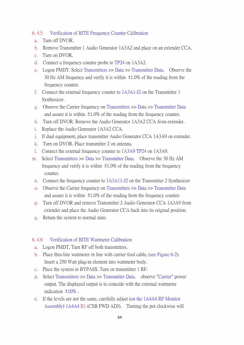
6. 4.6 Verification of BITE Wattmeter Calibration
a. Logon PMDT, Turn RF off both transmitters.
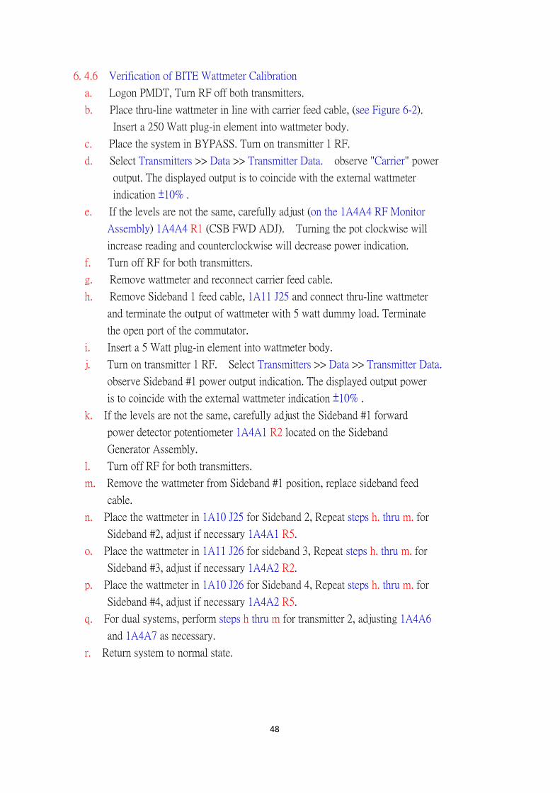
b. Place thru-line wattmeter in line with carrier feed cable, (see Figure 6-2).
Insert a 250 Watt plug-in element into wattmeter body.
c. Place the system in BYPASS. Turn on transmitter 1 RF.
d. Select Transmitters >> Data >> Transmitter Data. observe "Carrier" power
output. The displayed output is to coincide with the external wattmeter
indication ±10% .
e. If the levels are not the same, carefully adjust (on the 1A4A4 RF Monitor
Assembly) 1A4A4 R1 (CSB FWD ADJ). Turning the pot clockwise will
increase reading and counterclockwise will decrease power indication.
f. Turn off RF for both transmitters.
g. Remove wattmeter and reconnect carrier feed cable.
h. Remove Sideband 1 feed cable, 1A11 J25 and connect thru-line wattmeter
and terminate the output of wattmeter with 5 watt dummy load. Terminate
the open port of the commutator.
i. Insert a 5 Watt plug-in element into wattmeter body.
j. Turn on transmitter 1 RF. Select Transmitters >> Data >> Transmitter Data.
observe Sideband #1 power output indication. The displayed output power
is to coincide with the external wattmeter indication ±10% .
k. If the levels are not the same, carefully adjust the Sideband #1 forward
power detector potentiometer 1A4A1 R2 located on the Sideband
Generator Assembly.
l. Turn off RF for both transmitters.
m. Remove the wattmeter from Sideband #1 position, replace sideband feed
cable.
n. Place the wattmeter in 1A10 J25 for Sideband 2, Repeat steps h. thru m. for
Sideband #2, adjust if necessary 1A4A1 R5.
o. Place the wattmeter in 1A11 J26 for sideband 3, Repeat steps h. thru m. for
Sideband #3, adjust if necessary 1A4A2 R2.
p. Place the wattmeter in 1A10 J26 for Sideband 4, Repeat steps h. thru m. for
Sideband #4, adjust if necessary 1A4A2 R5.
q. For dual systems, perform steps h thru m for transmitter 2, adjusting 1A4A6
and 1A4A7 as necessary.
r. Return system to normal state.
49
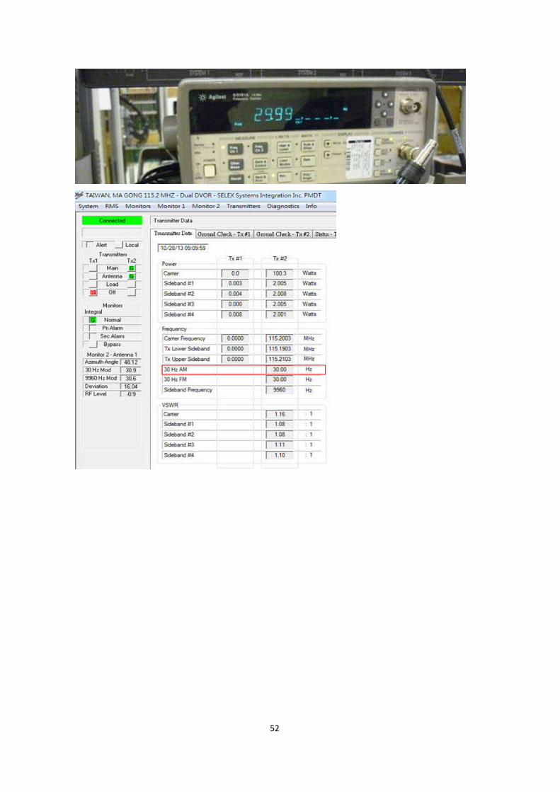
6.2.3 Carrier Frequency Performance Check
a. Verify that transmitter 1 is operating.
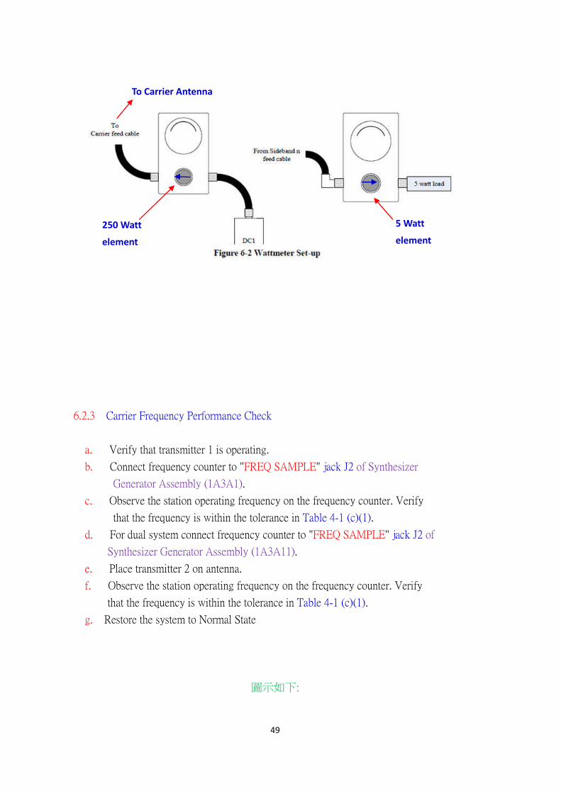
b. Connect frequency counter to "FREQ SAMPLE" jack J2 of Synthesizer
Generator Assembly (1A3A1).
c. Observe the station operating frequency on the frequency counter. Verify
that the frequency is within the tolerance in Table 4-1 (c)(1).
d. For dual system connect frequency counter to "FREQ SAMPLE" jack J2 of
Synthesizer Generator Assembly (1A3A11).
e. Place transmitter 2 on antenna.
f. Observe the station operating frequency on the frequency counter. Verify
that the frequency is within the tolerance in Table 4-1 (c)(1).
g. Restore the system to Normal State
圖示如下:
To Carrier Antenna
250 Watt
element
5 Watt
element
50
51
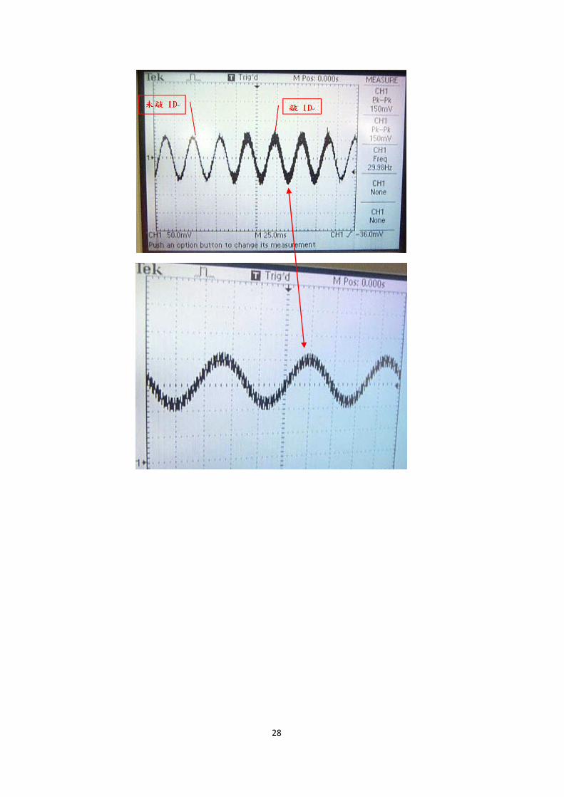
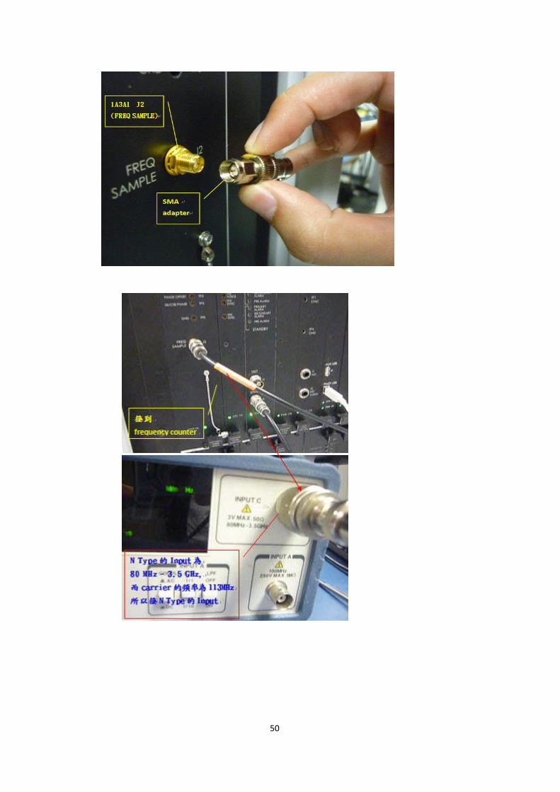
量到的值為: 112.9999 MHz
Audio Generator (1A3A2) TP24 延伸板
52
53
6.2.5 Modulation Frequency Performance Check
a. Verify that transmitter 1 is operating on antenna.
b. Select Transmitter >> Data >> Transmitter Data. View transmitter 1
parameters.
c. Verify that the 30 Hz AM frequency is within the tolerance of Table 4-1 (c)(4).
d. Verify the 30 Hz FM frequency is within the tolerance of Table 4-1 (c)(3).
e. Verify the 9960 Hz frequency is within the tolerance of Table 4-1 (c)(2).
NOTE
The frequencies displayed are measured with enough precision to certify the
operating tolerances of transmitter.
f. For dual transmitters place transmitter 2 on antenna.
g. Select Transmitter >> Data >> Transmitter Data. View transmitter 2
parameters.
h. Verify that the 30 Hz AM frequency is within the tolerance of Table 4-1 (c)(4).
i. Verify the 30 Hz FM frequency is within the tolerance of Table 4-1 (c)(3).
j. Verify the 9960 Hz frequency is within the tolerance of Table 4-1 (c)(2).
k. Restore the system to Normal State.
6.2.6 Antenna VSWR Performance Check
a. Verify that transmitter 1 is operating on antenna.
b. Select Transmitters >> Data >> Transmitter Data. Observe Carrier VSWR
for transmitter 1 and verify that this value is within the Operating Tolerance
of Table 4-1 (e)(1). If out of tolerance refer to Paragraph 6.4.4
c. On the same screen, observe Sideband 1, Sideband 2, Sideband 3, and
Sideband 4 VSWR. Verify that these values are within Operating Tolerance
of Table 4-1 (e)(1). If out of tolerance refer to Paragraph 6.4.4
d. Select Monitors >> Data >> Sideband Antenna VSWR observe the
sideband antenna VSWR. Verify that no antenna are out of tolerance as
indicated by an alert condition.
e. Restore the system to Normal State.
54
6.2.7 Automatic Transfer Performance Checks (Dual Equipment only)
a. Log on PMDT. Select Local mode. Select transmitter 1 as main.
b. Select Transmitters >> Configuration >> Nominal screen
and record Azimuth Index value.
c. Shift the Azimuth Index by an additional -3.0 degrees so that an
out-of-tolerance condition exists for Monitor 1 and Monitor 2. Press F7 to
apply.
d. Verify that transmitter 1 shut down. Verify approximately 20 seconds later
transmitter 2 is energized on antenna, then also shuts down.
e. Select RMS >> Config Restore to return to original condition.
f. Restore the system to Normal State.
6.2.8 VOR Monitor Performance Check
a. Select Monitor 1 >> Data >> Status Screen.
b. Verify that no maintenance alert indications are backlit in yellow.
c. Verify that no alarm indications are backlit in red.
d. Select Monitor 2 >> Data >> Status Screen.
e. Verify that no maintenance alert indications are backlit in yellow.
f. Verify that no alarm indications are backlit in red.
g. Restore the system to Normal State.
6.2.9 Monitor Integrity Test of DVOR Monitor (Refer to Section 3.6.8.2.2)
a. Select Monitor 1 >> Test Results >> Completed.
b. Verify Azimuth, 30 Hz modulation, 9960 Hz modulation, 9960 Hz deviation,
and Ident Modulation parameters have passed the Integrity test as
indicated by a green background for all parameters.
c. Select Monitor 2 >> Test Results >> Completed. Repeat step b. for Monitor 2.
NOTE
All VOR Monitor Integrity tests are performed continuously in the background. The current
status of the background test may be checked by selecting
Monitor 1 (or 2) >> Test Results >> In Process.
55
6.2.10 RSCU Operation Performance Check
WARNING
The following tests will remove the signal in space. A notice to airmen (NOTAM) must be
issued prior to starting this test and planned with Air Traffic Control personnel.
6.2.10.1 DVOR Equipment Performance Check
a. Logon PMDT. Select RMS >> Configuration >> General
b. Verify RCSU Configuration, "RCSU Present" box is selected.
c. Select RMS >> Status >> VOR Status verify "RCSU Connection Enabled"
status box is green.
d. Verify the "RCSU Communication Error" status box is green.
6.2.10.2 RCSU Equipment Performance Check (At RCSU location)
a. Verify communications are normal.
b. Remove status/control connection to VOR facility. Verify communications
fault exist.
c. Restore status/control connection to VOR facility. Verify communications
restored.
d. Turn off transmitter. Verify "transmitter off" indication is displayed.
e. Turn on transmitter. Verify "transmitter on" indication is displayed.
f. If dual transmitter configuration, change transmitters. Verify transmitter
change occurred. Place VOR system in "Local" mode. Verify alert
indication at RCSU. Exit "Local" mode.
g. Place VOR AC circuit breakers 1 and 2 to off. Verify maintenance alert occurs
h. Restore the system on normal state.
6.2.11 Identification Frequency and Modulation Level Checks
a. Place transmitter 1 on the antenna and place the monitors in bypass.
b. Connect Oscilliscope with test cable to Transmitter 1 Carrier Amplifier
1A5A3-P2. Select:
Transmitters >> Commands >> Transmitter Ident >> Continuous.
c. Set Transmitters >> Configuration >> Nominal >> Reference and Voice
Modulation to 0%.
d. Adjust the oscilliscope controls to obtain a pattern showing 2 or 3 cycles of
the 1020 identification modulation.
56
e. Measure the high and low peak voltages and calculate the modulation by the
following relation:
f. Verify that the modulation is within the tolerance of Table 4-1 (d)(4).
g. Measure the Ident frequency and verify it is within the tolerance of
Table 4-1 (c)(5).
h. Place transmitter 2 on antenna.
i. Connect oscilliscope test cable to Transmitter 2 Carrier Amplifier 1A5A4-P2.
j. Repeat steps d. e. f . g. for transmitter 2.
k. Restore system to normal state.
6.2.12 RMS Lithium Battery Check Procedure
a. Turn OFF DVOR.
b. Observing ESD precautions remove the 1A3A6 RMS CCA and place on an ESD
protective surface.
c. Verify JP1 is connected between pins 2-3 to enable battery backup.
d. Measure the DC voltage across the lithium battery B1.
e. Verify that the battery voltage is greater than or equal to 2.9 VDC at a room
temperature of 20±5°C.
f. If the battery voltage is not in tolerance, refer to Lithium Battery Procedure,
paragraph 6.4.7. Replace the RMS CCA, Turn ON DVOR.
g. Restore system to normal state.
6. 3 EQUIPMENT INSPECTION PROCEDURES
6. 3.1 Site Inspection
a. Check that the site is clear of any new obstructions or materials which could
affect the normal operation of the VOR system.
b. Check the shelter, inside and out, for any sign of water filtration, damage, or
other deterioration.
c. Check the condition of the air conditioner, shelter lighting, obstruction lights,
baseboard heaters, electrical outlets, lightening arrestors, etc.
d. Check for and remove any debris, accumulation of snow (over 4 inches, 10
cm), or ice (over 0.5 inches, 1.5 cm), on the field monitor antennas.
e. Check for and remove any accumulation of debris or snow (over 1 foot, 30
cm) on the counterpoise surface.
57
6. 3.2 Inspection of Transmission Antennas
a. Insure that both DVOR transmitters are turned off.
b. The DVR antennas are contained within fiberglass radomes.
c. Inspect the mating areas of the radomes where the radome interfaces with
the radome base or where the radome interfaces with the antennas. Check
for any signs of water leakage or deterioration. Repair or replace as
necessary.
d. If the radome shows water leakage, remove the radome and inspect the
antenna for any signs of deterioration of water damage. Replace or repair the
radome as necessary. Check the input cables and connectors for breaks,
cracks or corrosion. Check that the connectors are securely fastened, and
inspect the remaining parts of the antenna for damage or signs of vermin
infestation.
e. Inspect the counterpoise for any signs of deterioration, paying special
attention to the welded joints, bolted connections, mesh, etc. Check for
proper electrical connection between the counterpoise segments and
grounding connections. Corrosion should be corrected by removing rust and
applying paint or cold galvanizing spray.
f. Remove any articles carried into the radome area and replace the antenna
radome covers.
6. 3.3 Inspection of the Field Monitor Antenna
a. Inspect the condition of the field monitor antenna. Make sure it is solidly
mounted, and that all nuts and bolts are tightened.
b. Check the ground wire connection to earth ground, tighten connections if
necessary.
c. Inspect the condition of the field monitor antenna coaxial cables for signs of
cracks or breakage. Replace if necessary.
6. 3.4 Transmitter Cabinet Inspection
a. Visually inspect interconnecting wire harnesses, coaxial cables and
connectors for corrosion, cracks, breaks, and burns. Insure all RF
connectors are tightened.
b. Inspect all peripheral equipment to the DVOR, including the PMDT, printer,
etc.
c. Inspect the front panel indicators on the DVOR and assure that indicators are
normal.
58
6. 3.5 Battery Backup Unit Inspection
Refer to Figure 9-3
WARNING
Use extreme care when testing the batteries. The batteries may explode if handled or
connected improperly.
a. Place the Battery circuit breakers on the battery in the OFF position.
b. Remove the covers from the battery boxes. Visually inspect the condition of
each battery, and inspect the connectors and cables for any cracks, breaks,
burns, or corrosion. Make sure that all connectors are fastened tightly to
their terminals. Clean battery area if necessary.
c. Replace the battery box covers and place the circuit breakers in the ON
position.
6. 4 ALIGNMENT / MODULE REPLACEMENT PROCEDURES
6. 4.1 Battery Charging Power Supply (BCPS) Alignment Procedures
6. 4.1.1 System AC Voltage Alignment
a. Logon the PMDT. Place the VOR into the BYPASS STATE.
b. Use a Digital Volt Meter (DVM) to measure the AC input voltage between AC
Monitor (1A6) TB3 terminal 1 and 2 (TX POWER, LINE and NEUTRAL).
c. Select RMS >> Data >> Power supply Data, verify AC Input volts reading is
within 5 VAC of DVM measurement.
d. If not within 5 VAC, turn off the DVOR, remove the 1A5A1 BCPS and adjust
R30 a small amount. Replace the BCPS and turn on the DVOR. Verify the
AC Input volts is within 5 VAC of DVM measurement. Repeat this step as
necessary to achieve an in-tolerance condition.
e. For dual transmitter, Repeat step d. for transmitter 2, 1A5A2
f. Restore the system to NORMAL STATE.
6. 4.1.2 System AC Current Alignment
a. Turn off AC and DC circuit breakers.
b. At the shelter circuit breaker panel turn off AC power for the VOR station.
c. Disconnect the wire from the AC source to AC Monitor (1A6) TB3 position 1
(TX POWER, LINE).
d. Connect a Digital Volt Meter (DVM) configured for current measurement in
59
line with the wire from AC source to Monitor (1A6) TB3 position 1
(TX POWER, LINE). Set the DVM to measure AC current using a 10A scale.
e. Restore AC power to the VOR at the circuit breaker panel.
f. Turn on AC and DC circuit breakers.
g. Put the VOR into the BYPASS STATE.
h. Use the PMDT to display:
RMS >> RMS Data >> Power Supply Data , AC Input Amps and verify the
reading is within 0.3 amps of DVM reading
i. If not within 0.3 amps turn OFF DVOR, slide out the 1A5A1 BCPS a few
centimeters. Adjust 1A5A1 BCPS R56 a small amount. Replace the BCPS, Turn
ON DVOR. Re-check the current value. Repeat, as necessary so the :
RMS >> RMS Data >> Power Supply Data , AC Input Amps is within 0.3 amps.
j. Repeat procedure for transmitter 2, if installed, adjusting 1A5A2 BCPS.
k. Turn off TX1 and TX2 AC and DC circuit breakers.
l. At the shelter circuit breaker panel turn off AC power for the VOR station.
m. Remove the DVM and reconnect the AC line wire to the AC Monitor (1A6)
TB3 position 1.
n. Restore AC power to the VOR at the circuit breaker panel.
o. Restore the VOR to the NORMAL STATE.
6. 4.1.3 Obstruction Light AC Voltage Alignment
a. Use a Digital Volt Meter (DVM) configured for AC voltage to measure across
AC Monitor (1A6) TB1 position 1 and position 3.
NOTE
Terminal TB1-1 is normally connected to TB1-2 when a photo sensor is not used with the
obstruction light. When using a photo sensor the light opening must be covered with an
opaque object in order to force the obstruction light to turn on.
b. Use the PMDT to display:
RMS >> RMS Data >> Power Supply Data >>OB Light volts and verify the
reading is within 2 VAC of DVM measurement.
c. If not within 2 VAC turn OFF DVOR, slide out the 1A5A1 BCPS a few
centimeters. Adjust 1A5A1 BCPS R29 a small amount. Replace the BCPS,
Turn ON DVOR. Re-check the voltage value. Repeat, as necessary so the:
RMS >> RMS Data >> Power Supply Data >> OB Light volts is within 2 VAC
of DVM measurement.
60
d. Repeat procedure for transmitter 2, if installed, adjusting 1A5A2 BCPS.
e. Restore the VOR to the NORMAL STATE.
6. 4.1.4 Obstruction Light AC Current Alignment
a. Turn off DVOR.
b. At the shelter circuit breaker panel turn off AC power for the VOR station
including obstruction lights.
c. Disconnect the wire from the AC source to AC Monitor (1A6) TB1 position 2
(LINE).
d. Connect a Digital Volt Meter (DVM) in line with the wire from AC Monitor
(1A6) TB1 position 2 (OB LITE, LINE). Set the DVM to measure AC current
using a 10A scale.
NOTE
Terminal TB1-1 is normally connected to TB1-2 when a photo sensor is not used with the
obstruction light. When using a photo sensor the light opening must be covered with an
opaque object in order to force the obstruction light to turn on.
e. Disconnect any equipment connected to the front panel AC convenience
outlet on the 1A7 Status Panel.
f. Connect a Digital Volt Meter (DVM) in line with the wire from AC Monitor
(1A6) TB1 position 2 (OB LITE, LINE). Set the DVM to measure AC current
using a 10A scale.
g. Restore AC power to the VOR and obstruction light at the circuit breaker
panel.
h. Use the PMDT to display:
RMS >> RMS Data >> Power Supply Data >>OB Light Amps and verify the
reading is within 0.3 amps of DVM reading.
i. If not within 0.3 amps turn OFF DVOR, slide out the 1A5A1 BCPS a few
centimeters. Adjust 1A5A1 BCPS R44 a small amount. Replace the BCPS, Turn
ON DVOR. Re-check the current value. Repeat, as necessary so the :
RMS >> RMS Data >> Power Supply Data , OB Light Amps is within 0.3 amps.
j. Repeat procedure for transmitter 2 , if installed, adjusting 1A5A2 BCPS.
k. At the shelter circuit breaker panel turn off AC power for the VOR obstruction
lights.
l. Remove the DVM and reconnect the OB LITE line wire to the AC Monitor (1A6)
TB1 position 2.
61
m. Restore AC power to the VOR obstruction light at the circuit breaker panel.
n. Restore the VOR to the NORMAL STATE.
6. 4.2 Alarm Volume Adjustment Procedure
a. Locate the Volume adjust pot at the bottom right of the System Controls on
the 1A1 LCU.
b. Press the lamp test switch to activate the audio alarm.
c. Using the adjustment tool provided with the accessory kit, adjust the volume
pot to desired level.
d. Release the lamp test switch.
6. 4.3 RMS Facilities Exterior and Interior Temperature Calibration
a. If a precision thermometer is not available then skip this procedure.
b. Put the VOR into the BYPASS STATE.
c. Select RMS >> DATA >> Temperature Data. If an external Temperature
Sensor Assembly is connected to J7 of the 1A9 Interface CCA, verify the
displayed External Temperature is within 2 degrees of precision
thermometer. If not, turn OFF DVOR, slide out the 1A3A7 Facilities CCA a
few centimeters, adjust R41 a small amount. Replace the Facilities CCA,
Turn ON DVOR. Re-check the temperature value. Repeat, as necessary
adjusting 1A3A7 R41 until the PMDT "External Temperature" display matches
the temperature shown on an external thermometer.
d. Adjust 1A3A7 R42 using the technique in step c until the
"Inside Temperature" display matches the temperature shown on an internal
thermometer as it is located near the 1A9 Interface CCA.
e. Restore the VOR to the NORMAL STATE.
6. 4.4 Verification of BITE VSWR Calibration
a. Turn both transmitters off.
b. Disconnect the Carrier feed cable from the top of the DC1 directional coupler
in the DVOR cabinet. Connect a type "N" male-male barrel to the
directional coupler. Connect a type "N" all female TEE to the barrel and
attach an appropriate dummy load to the TTE. Attach type "N" male-male
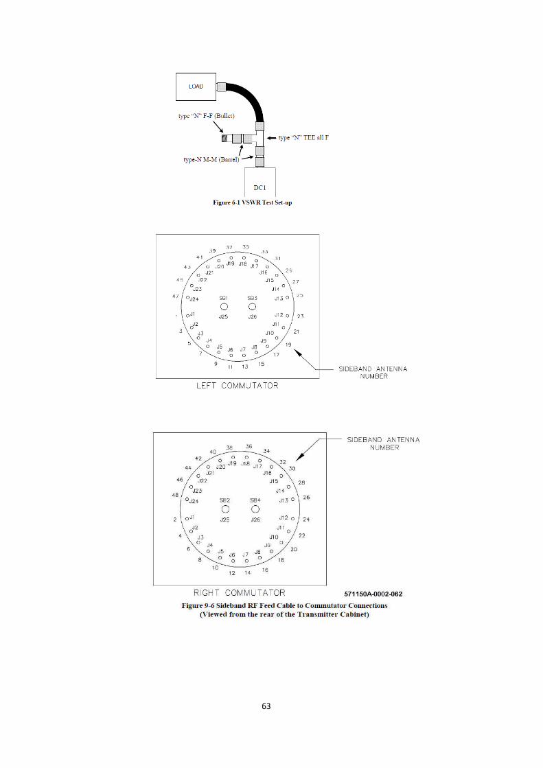
barrel and type "N" female-female bullet (see Figure 6-1 for test set-up) to
the remaining open port of the TEE. This simulates a 1.22 : 1 load. If a 250
62
Watt load is not available a 25 Watt load may be used for less than 1 minute
for this test.
Load : 250 W 的 dummy load
Load : 25 W 測試時間須低於 1 分鐘
c. Place system in BYPASS. Turn on transmitter 1.
d. Select screen: Transmitters >> Data >> Transmitter Data, observe Carrier
VSWR. The display VSWR should be between 1.20 to 1.23
e. If the level is not within this range, carefully adjust (on the 1A4A4 RF Monitor
Assembly) the transmitter reflected power detector potentiometer 1A4A4 R2
(CSB RFL ADJ) until reading is within range. Turning the pot clockwise will
increase VSWR reading and counterclockwise will decrease. Make a small
adjustment and wait for display to stabilize.
f. Turn RF off for both transmitters.
g. Move the barrel, bullet, and TEE to the Sideband 1 feed cable at 1A11 J25 (see
Figure 9-6 for location). Place an appropriate dummy load on the TEE output,
terminate the open port of the commutator. Place the Carrier Transmitter
cable back to its original position.
h. Turn on transmitter 1.
i. Select screen Monitors >> Data >> Sideband Antenna VSWR, observe odd
numbered Antenna VSWR. The displayed VSWR should be 1.20 ± 0.15 for
odd numbered antennae. If not within range then the 1A4A1 sideband
amplifier (with built-in VSWR measurement circuitry) should be replaced.
j. Turn RF off for both transmitters. Move the load, barrel, bullet, and TEE to the
Sideband 2 feed cable at 1A10 J25 (see Figure 9-6 for location). Terminate the
open port of the commutator.
k. Turn on both transmitters. Select screen :
Monitors >> Data >> Sideband Antenna VSWR, observe even numbered
Antenna VSWR. The displayed VSWR should be 1.20 ± 0.15 for
even numbered antennae. If not within range then the 1A4A1 sideband
amplifier (with built-in VSWR measurement circuitry) should be replaced.
l. Turn off both transmitters. Remove termination, TEE with barrel and bullet.
Place cables in their original positions.
m. Return the system to normal state.
63
64
6. 4.5 Verification of BITE Frequency Counter Calibration
a. Turn off DVOR.
b. Remove Transmitter 1 Audio Generator 1A3A2 and place on an extender CCA.
c. Turn on DVOR.
d. Connect a frequency counter probe to TP24 on 1A3A2.
e. Logon PMDT. Select Transmitters >> Data >> Transmitter Data. Observe the
30 Hz AM frequency and verify it is within ±1.0% of the reading from the
frequency counter.
f. Connect the external frequency counter to 1A3A1-J2 on the Transmitter 1
Synthesizer.
g. Observe the Carrier frequency on Transmitters >> Data >> Transmitter Data
and assure it is within ±1.0% of the reading from the frequency counter.
h. Turn off DVOR. Remove the Audio Generator 1A3A2 CCA from extender.
i. Replace the Audio Generator 1A3A2 CCA.
j. If dual equipment, place transmitter Audio Generator CCA 1A3A9 on extender.
k. Turn on DVOR. Place transmitter 2 on antenna.
l. Connect the external frequency counter to 1A3A9 TP24 on 1A3A9.
m. Select Transmitters >> Data >> Transmitter Data. Observe the 30 Hz AM
frequency and verify it is within ±1.0% of the reading from the frequency
counter.
n. Connect the frequency counter to 1A3A11-J2 on the Transmitter 2 Synthesizer
o. Observe the Carrier frequency on Transmitters >> Data >> Transmitter Data
and assure it is within ±1.0% of the reading from the frequency counter.
p. Turn off DVOR and remove Transmitter 2 Audio Generator CCA 1A3A9 from
extender and place the Audio Generator CCA back into its original position.
q. Return the system to normal state.
6. 4.6 Verification of BITE Wattmeter Calibration
a. Logon PMDT, Turn RF off both transmitters.
b. Place thru-line wattmeter in line with carrier feed cable, (see Figure 6-2).
Insert a 250 Watt plug-in element into wattmeter body.
c. Place the system in BYPASS. Turn on transmitter 1 RF.
d. Select Transmitters >> Data >> Transmitter Data. observe "Carrier" power
output. The displayed output is to coincide with the external wattmeter
indication ±10% .
e. If the levels are not the same, carefully adjust (on the 1A4A4 RF Monitor
Assembly) 1A4A4 R1 (CSB FWD ADJ). Turning the pot clockwise will
65
increase reading and counterclockwise will decrease power indication.
f. Turn off RF for both transmitters.
g. Remove wattmeter and reconnect carrier feed cable.
h. Remove Sideband 1 feed cable, 1A11 J25 and connect thru-line wattmeter
and terminate the output of wattmeter with 5 watt dummy load. Terminate
the open port of the commutator.
i. Insert a 5 Watt plug-in element into wattmeter body.
j. Turn on transmitter 1 RF. Select Transmitters >> Data >> Transmitter Data.
observe Sideband #1 power output indication. The displayed output power is
to coincide with the external wattmeter indication ±10% .
k. If the levels are not the same, carefully adjust the Sideband #1 forward power
detector potentiometer 1A4A1 R2 located on the Sideband Generator
Assembly.
l. Turn off RF for both transmitters.
m. Remove the wattmeter from Sideband #1 position, replace sideband feed
cable.
n. Place the wattmeter in 1A10 J25 for Sideband 2, Repeat steps h. thru m. for
Sideband #2, adjust if necessary 1A4A1 R5.
o. Place the wattmeter in 1A11 J26 for sideband 3, Repeat steps h. thru m. for
Sideband #3, adjust if necessary 1A4A2 R2.
p. Place the wattmeter in 1A10 J26 for Sideband 4, Repeat steps h. thru m. for
Sideband #4, adjust if necessary 1A4A2 R5.
q. For dual systems, perform steps h thru m for transmitter 2, adjusting 1A4A6
and 1A4A7 as necessary.
r. Return system to normal state.
To Carrier Antenna
250 Watt
element
5 Watt
element
66
6. 4.7 RMS (1A3A6) Lithium Battery Replacement Procedure
a. Logon PMDT Select System >> Configuration Save. Select or create a
distinctive filename and location to save the current system configuration
and click save.
b. Logoff PMDT
c. Turn OFF DVOR.
d. Observing ESD precautions, remove RMS CCA (1A3A6) and replace the
battery.
e. Place the RMS CCA into the cabinet and seat securely into backplane
connector.
f. Turn on DVOR
g. Logon PMDT, Place the VOR in LOCAL mode.
h. Select System >> Configuration Load, and select the Filename saved in Step a.
i. Select RMS >> Config Backup.
j. Return the system to NORMAL STATE.
6. 4.8 Update of DVOR Software
NOTE
During the product life cycle software updates may become available for the VOR product in
service. The RMS, Monitor and Audio Generator software is updated through the PMDT port
using a SELEX-SI software product called "Flash loader"
Please refer to the installation instructions accompanying the software update service bulletin
for detailed software upgrade procedures.
a. On the PMDT Select System >> Configuration Save. Select or create a
distinctive filename and location to save the current system configuration
and click save.
b. Perform the software update per the instruction provided.
c. Place the VOR in LOCAL mode. Select System >> Configuration Load, and
select the Filename saved in Step a.
d. Select RMS >> Config Backup
e. Return the system to NORMAL STATE
67
6. 4.9 Changing the Station Rotation (Azimuth)
This step may be requested during a flight inspection of the VOR station.
a. Select Transmitters >> Configuration >> Offsets and Scale Factors. Adjust the
Azimuth angle offset for Transmitter 1 and/or Transmitter 2 as requested by
flight inspection or reference value.
b. Enter a more positive number for clockwise rotation or a more negative
number for counterclockwise rotation. The allowable entry is ±20 degrees
in 0.01 degree increments.
c. If any changes are made, select RMS >> Config Backup. Save file as required.
d. Return the system to NORMAL STATE.
6. 4.10 Changing the Monitoring Offsets
This procedure is required after commissioning flight check to make the monitors agree with
flight inspection results.
a. Turn on Transmitter 1.
b. Select Monitor 1 or 2 >> Data >> Integral observe parameters.
c. If changes are necessary to make monitors display correct value, select
Monitor 1 or 2 >> Offsets and Scale Factors. Enter the amount of offset
necessary to provide proper indication on Monitor 1 or 2 >> Data >> Integral.
d. If changes were made, select RMS >> Config Backup. Save file as required.
e. return system to NOMAL STATE.
6. 4.11 DME Keying Check
This procedure is used on systems where the DVOR is collocated with a DME.
a. Place the system to NORMAL STATE.
b. Select RMS >> Commands >> Select Audio >> Transmitter 1 Ident.
c. Place DME in normal state.
d. Verify audible DME keying. Select (on SELEX-SI DME)
RMS >> Commands >> Select Audio >> Transmitter 1 Ident.
e. If keying is not detected or is not in synchronization with the DVOR check
terminal board wiring and connections.
f. Return both systems to NORMAL STATE.
68
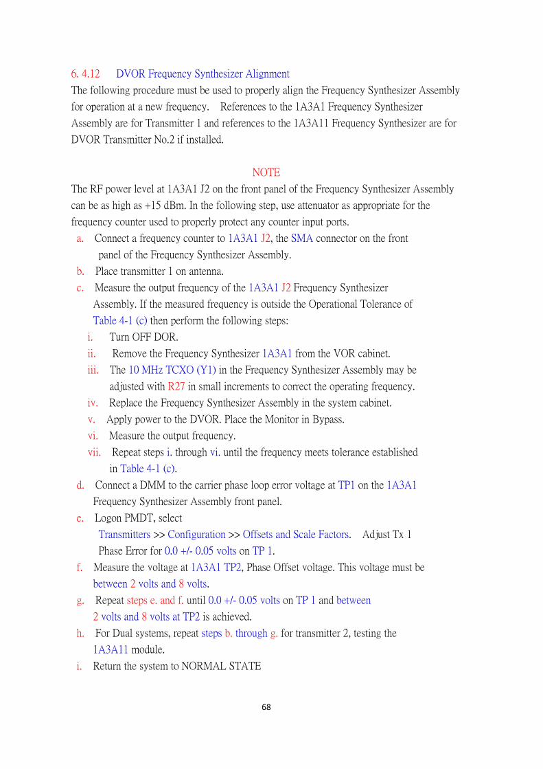
6. 4.12 DVOR Frequency Synthesizer Alignment
The following procedure must be used to properly align the Frequency Synthesizer Assembly
for operation at a new frequency. References to the 1A3A1 Frequency Synthesizer
Assembly are for Transmitter 1 and references to the 1A3A11 Frequency Synthesizer are for
DVOR Transmitter No.2 if installed.
NOTE
The RF power level at 1A3A1 J2 on the front panel of the Frequency Synthesizer Assembly
can be as high as +15 dBm. In the following step, use attenuator as appropriate for the
frequency counter used to properly protect any counter input ports.
a. Connect a frequency counter to 1A3A1 J2, the SMA connector on the front
panel of the Frequency Synthesizer Assembly.
b. Place transmitter 1 on antenna.
c. Measure the output frequency of the 1A3A1 J2 Frequency Synthesizer
Assembly. If the measured frequency is outside the Operational Tolerance of
Table 4-1 (c) then perform the following steps:
i. Turn OFF DOR.
ii. Remove the Frequency Synthesizer 1A3A1 from the VOR cabinet.
iii. The 10 MHz TCXO (Y1) in the Frequency Synthesizer Assembly may be
adjusted with R27 in small increments to correct the operating frequency.
iv. Replace the Frequency Synthesizer Assembly in the system cabinet.
v. Apply power to the DVOR. Place the Monitor in Bypass.
vi. Measure the output frequency.
vii. Repeat steps i. through vi. until the frequency meets tolerance established
in Table 4-1 (c).
d. Connect a DMM to the carrier phase loop error voltage at TP1 on the 1A3A1
Frequency Synthesizer Assembly front panel.
e. Logon PMDT, select
Transmitters >> Configuration >> Offsets and Scale Factors. Adjust Tx 1
Phase Error for 0.0 +/- 0.05 volts on TP 1.
f. Measure the voltage at 1A3A1 TP2, Phase Offset voltage. This voltage must be
between 2 volts and 8 volts.
g. Repeat steps e. and f. until 0.0 +/- 0.05 volts on TP 1 and between
2 volts and 8 volts at TP2 is achieved.
h. For Dual systems, repeat steps b. through g. for transmitter 2, testing the
1A3A11 module.
i. Return the system to NORMAL STATE
69
6.4.13 Antenna VSWR Check for New Frequency
All of the radiating antennas in the DVOR antenna system were installed with an initial
VSWR that was less than 1.10:1 (Table 4-1a). DVOR antennas are narrow-band devises that
are critically tuned using mechanical components (stubs, positioning pieces, and capacitors)
to produce a resonant antenna that is matched to a 50 ohm impedance feed cable. Any
significant change in the operating frequency of the DVOR will change the resonant point of
operation of the antenna and that will affect the VSWR of the antenna and the signal in space
of the DVOR system. Perform the following procedures to determine of there is a need to
return the antenna system.
a. Turn OFF DVOR.
b. Install a power meter (Bird model 43 or equivalent) in the carrier antenna
feed cable.
c. Install an appropriate detecting element in the wattmeter to measure forward
power.
d. Turn ON DVOR and record the DVOR carrier forward power indicated on the
wattmeter.
e. Install an appropriate detecting element in the wattmeter to measure
reflected power.
f. Record the DVOR reflected power.
g. Calculate the VSWR of the Carrier Antenna using the formula:
h. If the calculated VSWR exceedes 1.20:1, refer to Antenna Manual,
P/N 570002-0001.
6.4.14 1A3A1/1A3A11 Synthesizer Replacement
a. Logon PMDT Select System >> Configuration Save. Select or create a
distinctive filename and location to save the current system configuration
and click save.
b. Logoff PMDT
c. Turn OFF DVOR
d. Observing ESD precautions, remove Synthesizer CCA (1A3A1/1A3A11) and
insert the new Synthesizer CCA into the cabinet and seat securely into
backplane connector.
e. Turn on DVOR.
f. Place the DVOR in LOCAL mode.
70
g. Logon PMDT Select System >> Configuration Load, and select the Filename
saved in Step a.
h. Select RMS >> Config Backup.
i. Perform paragraph 6.4.12 DVOR Frequency Synthesizer Alignment.
j. Return the system to NORMAL STATE.
6.4.15 1A3A2/1A3A9 Audio Generator Replacement
a. Logon PMDT. Select System >> Configuration Save. Select or create a
filename and location to save the current system configuration and click save.
b. Turn OFF DVOR.
c. Remove and replace 1A3A2 (or 1A3A9 for dual transmitter systems) Audio
Generator.
d. Turn ON DVOR.
e. Logon PMDT, Place the system in bypass.
NOTE
The system will automatically load the last saved configuration.
f. Select Monitors >> Integral, verify all parameters are within tolerance.
g. Select Transmitters >> Data >> Transmitter Data, Verify all parameters are
within tolerance.
h. Return the system to NORMAL STATE.
6.4.16 1A3A3/1A3A10 Monitor Replancement
a. Logon PMDT. Select System >> Configuration Save. Select or create a
filename and location to save the current system configuration and click save.
b. Logoff PMDT
c. Turn OFF DVOR.
d. Observing ESD precautions, remove Monitor CCA (1A3A3/1A3A10) and insert
the new Monitor CCA into the cabinet and seat securely into backplane
connector.
e. Turn on DVOR
f. Place the DVOR in LOCAL mode.
g. Logon on PMDT Select System >> Configuration Load, and select the Filename
saved in Step a.
h. Select RMS >> Config Backup
71
i. Perform paragraph 6.4.10 changing the Monitoring Offsets.
j. Return the system to NORMAL STATE.
6.4.17 1A3A4/1A3A8 LVPS Replacement
a. Turn OFF DVOR
b. Observing ESD precautions, remove LVPS CCA (1A3A4/1A3A8) and insert
the new LVPS CCA into the cabinet and seat securely into backplane
connector.
c. Turn ON DVOR
d. Logon PMDT. Select RMS >> Data >> Power Supply Data. Verify voltages are
within operating tolerance.
e. Select RMS >> Data >> Digital I/O. Verify “Power Supply Status” is operating
normally with green background.
f. Return the system to NORMAL STATE.
6.4.18 1A3A5 Test Generator Replacement
a. Turn OFF DVOR
b. Observing ESD precautions, remove Test Generator CCA (1A3A5) and insert
the new Test Generator CCA into the cabinet and seat securely into
backplane connector.
c. Turn ON DVOR
d. Logon PMDT. Select Monitor 1 >> Teat Results >> Completed. Wait three
minutes for the test to complete. Verify all monitored parameters are
operating normally with green background.
f. Return the system to NORMAL STATE.
6.4.19 (1A3A6) RMS CPU Replacement
a. Logon PMDT Select System >> Configuration Save. Select or create a
distinctive filename and location to save the current system configuration
and click save.
b. Logoff PMDT
c. Turn OFF DVOR
d. Observing ESD precautions, remove RMS CCA (1A3A6) and insert the new
RMS CCA into the cabinet and seat securely into
backplane connector.
72
c. Turn ON DVOR
d. Place the DVOR in LOCAL mode.
e. Logon on PMDT Select System >> Configuration Load, and select the Filename
saved in Step a.
f. Select RMS >> Config Backup
g. Return the system to NORMAL STATE.
6.4.20 1A3A7 Facilities Replacement
a. Turn OFF DVOR
b. Observing ESD precautions, remove Facilities CCA (1A3A7) and insert the new
Facilities CCA into the cabinet and seat securely into backplane
connector.
c. Turn ON DVOR
d. Logon PMDT. Select RMS >> Data >> Power Supply Data. Verify voltages are
within operating tolerance.
e. Select RMS >> Data >> Digital I/O. Verify “Facilities” is operating normally
with green background.
f. Return the system to NORMAL STATE.
6.4.21 1A4A4 RF Monitor Replacement
a. Turn OFF DVOR
b. Observing ESD precautions, remove RF Monitor CCA (1A4A4) and insert the
new RF monitor CCA into the cabinet and seat securely into backplane
connector.
c. Turn ON DVOR
d. Logon PMDT
e. Perform paragraphs 6.4.6 Verification of BITE Wattmeter Calibration and
6.4.13 Antenna VSWR Check.
f. Select Monitors >> Data >> Sideband Antenna VSWR. Verify all “Antenna
VSWRs” are operating normally with green background.
g. Return the system to NORMAL STATE.
73
6.4.22 1A5A1/1A5A2 BCPS Replacement
a. Turn OFF DVOR
b. Observing ESD precautions, remove BBCPS CCA (1A5A1, 1A5A2) and insert
the new BCPS CCA into the cabinet and seat securely into backplane
connector.
c. Turn ON DVOR
d. Perform paragraph 6.4.1.1 System AC Voltage Alignment and 6.4.1.2 System
AC Current Alignment.
e. Logon PMDT. Select RMS >> Data >> Power Supply Data and verify the
“TX1/TX2 48V PS1/PS2 is operating normally with no alarm indication.
Select RMS >> Data >> Digital I/O and verify the “48V PS” and “BCPS PS”.
f. Return the system to NORMAL STATE.
6.4.23 1A5A3/1A5A4 CSB AMP Replacement
a. Turn OFF DVOR
b. Observing ESD precautions, remove CSB AMP (1A5A1/1A5A2) and insert the
new CSB AMP into the cabinet and seat securely into backplane connector.
c. Turn ON DVOR
d. Logon PMDT. Place the system in Bypass. Place the system in Local control.
Place transmitter on the antenna ( transmitter of replaced CSB AMP ).
Select Transmitters >> Transmitter Data. View “Carrier” power.
If the output power is not the reference value +/- 5%, Select:
Transmitters >> Configuration >> Offsets and Scale Factors and adjust
“Output Power Scale” to set the output power to the reference value.
Select RMS >> Config Backup. Save the file as necessary.
e. Return the system to NORMAL STATE.
6.4.24 1A4A1/1A4A2/1A4A6/1A4A7 DVOR Sideband Amplifier Replacement,
Performance Check, Alignment
Perform the following steps to replace a sideband amplifier. This procedure may also be used
as a performance check.
a. Turn OFF DVOR
b. Remove 1A4A1 (Sideband #1 #2) or 1A4A2 (Sideband #3 #4)
c. Install replacement module.
d. Turn ON VOR
e. Place the system in bypass. Place transmitter 1 on the antenna.
74
f. Connect a DVM to 1A4A1 TP1, SB1 PHS DET, adjust R1 voltage between
0.90 and 0.95 Vdc.
g. Connect a DVM to 1A4A1 TP5, PHS ERROR, adjust R1 voltage between
0.89 and 0.91 Vdc.
h. Connect a DVM to 1A4A1 TP4, MEAN/DYN PHS, verify voltage is between
2 and 9 Vdc, if not then adjust R1. If still unable to achieve 2 to 9 Vdc range,
Turn OFF DVOR, slide out the subject sideband amplifier several centimeters,
place jumper J11 from present position to opposite position.
Example: if jumper is in position 1-2, move it to 3-4.
Repeat steps c. through g.
i. Connect a DVM to 1A4A1 TP7, SB1 PHS DET, adjust R4 voltage between
0.90 and 0.95 Vdc.
j. Connect a DVM to 1A4A1 TP11, PHS ERROR, adjust R4 voltage between
0.89 and 0.91 Vdc.
k. Connect a DVM to 1A4A1 TP10, MEAN/DYN PHS, verify voltage is between
2 and 9 Vdc, if not then adjust R4.
l. Perform steps a. through g. for Sideband Amplifier 1A4A2 if applicable.
m. Logon PMDT. Select Transmitters>>Configuration >>Offsets and Scale Factors,
adjust both "Sideband Phase Offset" values of the replaced unit to zero.
Adjust either "Sideband Phase Offset" value to achieve 0.0 Vdc +/- 0.1 Vdc at
1A4A1 TP6. Set the final "Sideband Phase Offset" value so that difference is
centered about 0 degrees phase shift. For example if 10 degrees difference
between Sideband 1 and Sideband 2 is required then set Sideband 1 to -5
degrees and Sideband 2 to +5 degrees.
n. Logon PMDT. Select Transmitters>> Configuration>> Offsets and Scale Factors,
adjust subject "Sideband RF Level Scale" to 100.
o. Adjust subject sideband amplifier for reference sideband power value
(R3 for sideband 1 or 3, R6 for sideband 2 or 4).
p. Select RMS >> Config Backup. Save the configuration file as necessary.
q. Return the system to NORMAL STATE.
75
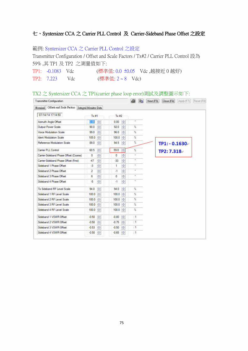
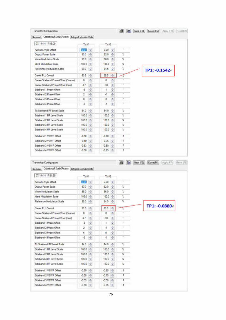
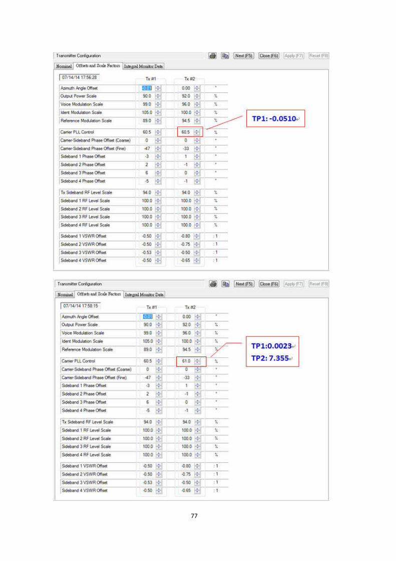
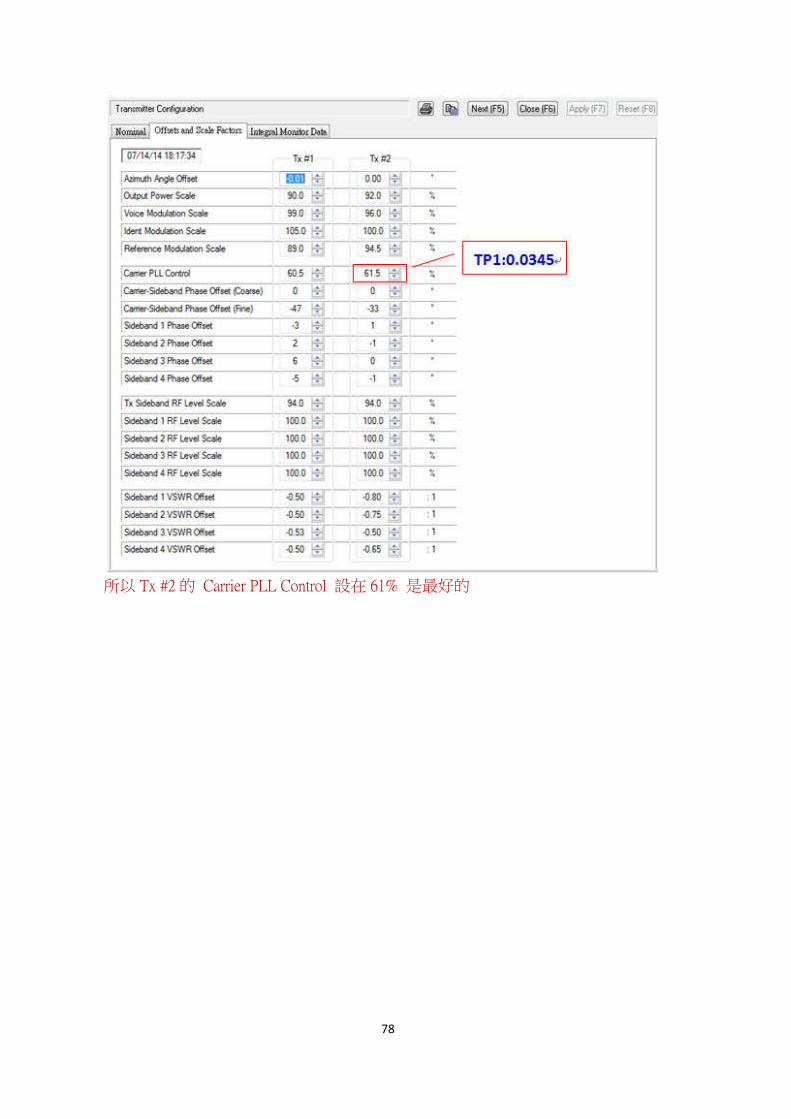
七七七七、、、、SyntersizerSyntersizerSyntersizerSyntersizer CCACCACCACCA 之之之之 Carrier PLL Control Carrier PLL Control Carrier PLL Control Carrier PLL Control 及及及及 CarrierCarrierCarrierCarrier----Sideband Phase OffsetSideband Phase OffsetSideband Phase OffsetSideband Phase Offset 之設定之設定之設定之設定
範例: Syntersizer CCA 之 Carrier PLL Control 之設定
Transmitter Configuration / Offset and Scale Factors / Tx#2 / Carrier PLL Control 設為
59% ,其 TP1 及 TP2 之測量值如下:
TP1: -0.1083 Vdc (標準值: 0.0 ±0.05 Vdc ,越接近 0 越好)
TP2: 7.223 Vdc (標準值: 2 ~ 8 Vdc)
TX2 之 Syntersizer CCA 之 TP1(carrier phase loop error)測試及調整圖示如下:
76
77
78
所以 Tx #2 的 Carrier PLL Control 設在 61% 是最好的

79
範例: Syntersizer CCA 之 Carrier-Sideband Phase Offset 之設定
sideband to carrier phasing
Step 1 – With transmitter 1 on the antenna, while observing the sidebar
9960 Hz Mod, adjust Transmitters, Configuration, Offsets and Scale Factors,
TX#1 column, Carrier-Sideband Phase Offset (Fine). Adjust the value in
degrees up and down until the highest value of 9960 Hz modulation is
achieved. If the adjustment is causing larger values but comes to an end
at -55 degrees, then reduce the value of Carrier-Sideband Phase Offset
(Coarse) down by 90 degrees. Then go back and continue adjusting the Fine
offset until the maximum value for 9960 Hz Modulation is found.
IMPORTANT – Don’t stop adjusting once 30% is achieved. The value of 9960
Hz Mod MUST be the MAXIMUM that can be found. Don’t worry, it will be
readjusted at the end for 30%. (FOR EXAMPLE: you may be able to achieve
32.7%. This is fine for now.)
Step 2 – Take note of the value of Fine offset degrees. (FOR EXAMPLE: you
may read -42 degrees.) If the value is negative, then subtract a few
degrees, up to 15 if it is possible, but fewer degrees if 15 is not
possible. (FOR EXAMPLE: -42 minus 13 degrees = -55 degrees – the lowest
value possible.) If the value is positive, then add a few degrees, up to 15
degrees of change. When this change is made, it will cause the 9960 Hz
modulation to reduce. (FOR EXAMPLE: you may now read 29.4%.) Take note of
the 9960 Hz modulation reading, and how much it reduced.
Step 3 – Now, from the original setting of the Fine offset degrees, adjust
the setting in the opposite direction until the same reduction in 9960 Hz
Mod is achieved. (TO FOLLOW THE EXAMPLE: Add from -42, going positive until
the 9960 Hz mod reads 29.4%). Take note of this Fine offset setting.
(EXAMPLE: perhaps it is necessary to change the degrees to -20 do achieve
29.4%.)
Step 4 – Take the average of the two de-phased settings (IN THE EXAMPLE:
Add -55 plus -20 = -72, divided by two = -36). Enter this value as the
Fine offset setting.
If this all went well, then the 9960 Hz Modulation value should be equal to,
80
or even greater than, what was able to be found before. (FOR EXAMPLE, you
may now measure 32.8%. This is better than before.)
Step 5 – NOW change the value of TX Sideband RF Level Scale up or down to
achieve 9960 Hz modulation value of exactly 30.0%.
Step 6 – Transfer to place transmitter #2 on antenna and repeat steps 1-5.
Step 7 – Back up these values.
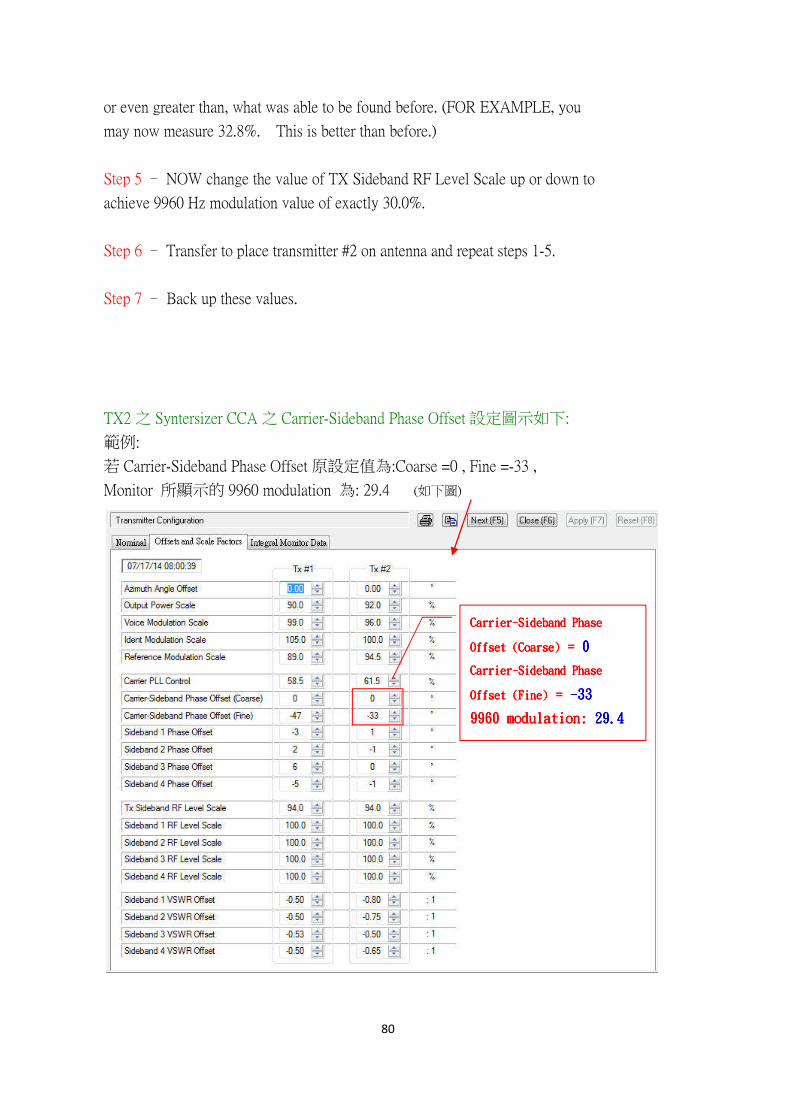
TX2 之 Syntersizer CCA 之 Carrier-Sideband Phase Offset 設定圖示如下:
範例:
若 Carrier-Sideband Phase Offset 原設定值為:Coarse =0 , Fine =-33 ,
Monitor 所顯示的 9960 modulation 為: 29.4 (如下圖)
CarrierCarrierCarrierCarrier----Sideband Phase Sideband Phase Sideband Phase Sideband Phase
Offset (Coarse)Offset (Coarse)Offset (Coarse)Offset (Coarse) = = = = 0000
CarrierCarrierCarrierCarrier----Sideband Phase Sideband Phase Sideband Phase Sideband Phase
Offset (Offset (Offset (Offset (FineFineFineFine)))) = = = = ----33333333
9960 9960 9960 9960 modulation:modulation:modulation:modulation: 29.429.429.429.4
81
原設定值為:
Carrier-Sideband Phase Offset (Coarse) :0
Carrier-Sideband Phase Offset (Fine) :-33 ,
9960 modulation: 29.4
修改 Carrier-Sideband Phase Offset (Fine)的值及其修改後之
9960 modulation 分別如下:
-36: 29.4 -35: 29.4 -34: 29.5
-33: 29.6 -32: 29.7 -31: 29.8 -30: 30.0
-29: 30.0 -28: 30.1 -27: 30.1 -26: 30.1
-25: 30.2 -24: 30.3 -23: 30.4
-22: 30.5
-21: 30.6 最大值,因為-21 是負的所以減 15 = -36 其值為 29.4
依相反的方向找到 3 其值為 29.4
所以 Fine 的最佳值為: (-36+ 3)/2 = -16 , -17
因因因因----17171717 的的的的 9960 modulation9960 modulation9960 modulation9960 modulation 比比比比----16161616 好好好好,,,,所以取所以取所以取所以取 ----17171717
-20: 30.6
-19: 30.6 -18: 30.6 ----17:17:17:17: 30.630.630.630.6 -16: 30.6 ~ 30.5
-15: 30.5 -14: 30.4 -13: 30.3 -12: 30.2
-11: 30.2 -10: 30.2 -9: 30.1 -8: 30.1
-7: 30.1 -6: 30.0 -5: 30.0 -4: 29.9
-3: 29.9 -2: 29.8 -1: 29.8 0: 29.7 1: 29.6
2: 29.5 3: 29.4
82
八八八八、、、、Sideband Phase Offset Sideband Phase Offset Sideband Phase Offset Sideband Phase Offset 設定設定設定設定
Sideband Amplifier CCA 的 TP 6 量測值須為: 0.0 Vdc +/- 0.1 Vdc(越接近 0 越好)
範例:
TX1 之 Sideband 3 Phase Offset 與 Sideband 4 Phase Offset 設定圖示如下:
83
所以 TX1 之 Sideband 3 Phase Offset 設為 5 而 Sideband 4 Phase Offset 設為-5 是最好
的
84
九九九九、、、、飛測調整飛測調整飛測調整飛測調整
注意事項:
1.1.1.1. 調整參數時須設在 Local,參數才能調整。
2. 調整參數時須設在 Bypass 的狀態,以防調整過程造成當機 。
Reference Modulation 調整
9960 Modulation 調整
85
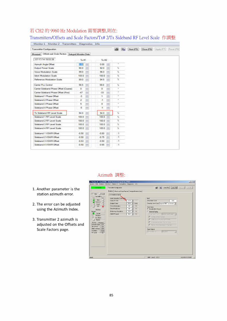
若 CH2 的 9960 Hz Modulation 需要調整,則在:
Transmitters/Offsets and Scale Factors/Tx# 2/Tx Sideband RF Level Scale 作調整
Azimuth 調整:
86
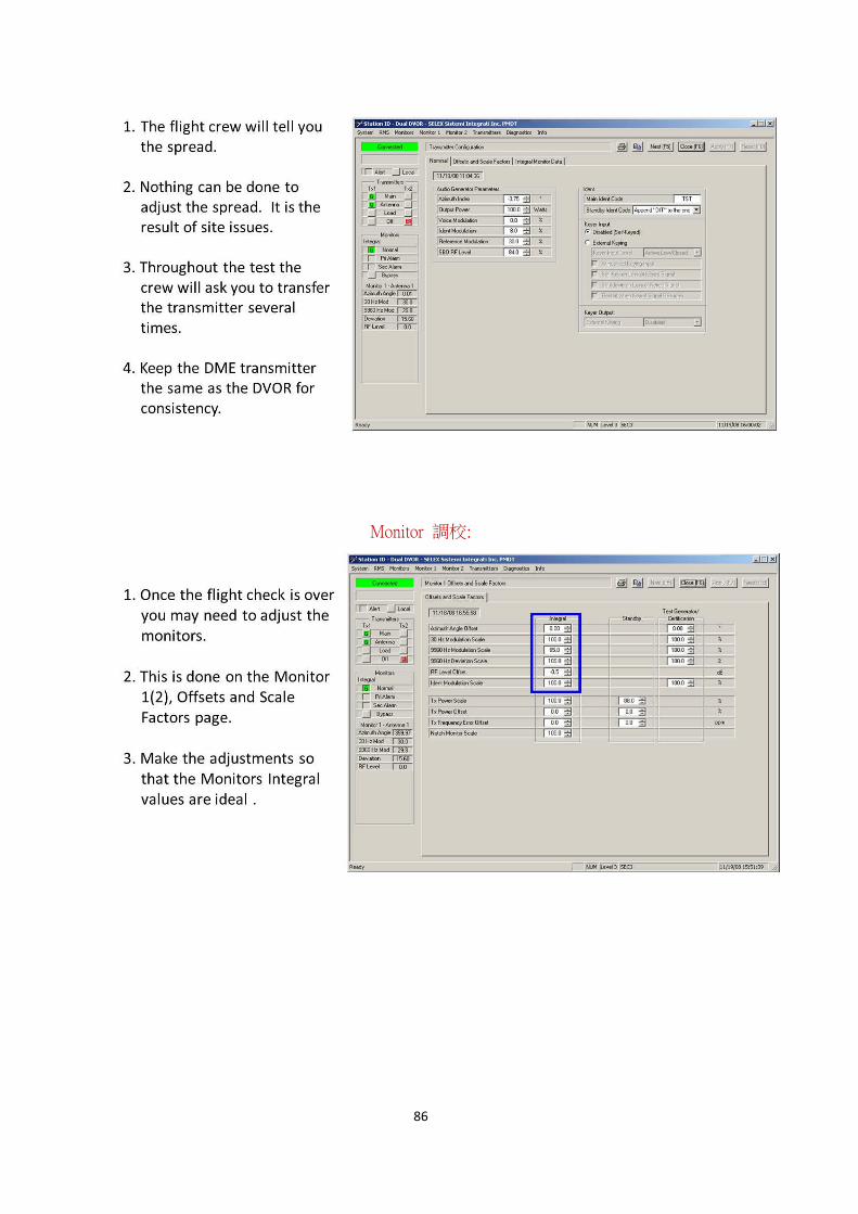
Monitor 調校:
87
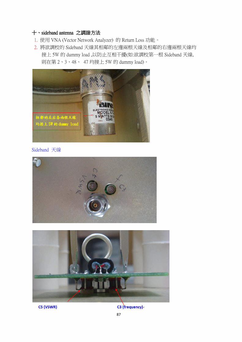
十十十十、、、、sideband antenna sideband antenna sideband antenna sideband antenna 之調諧方法之調諧方法之調諧方法之調諧方法
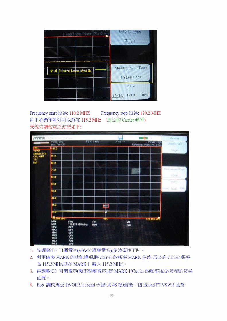
1. 使用 VNA (Vector Network Analyzer) 的 Return Loss 功能。
2. 將欲調校的 Sideband 天線其相鄰的左邊兩根天線及相鄰的右邊兩根天線均
接上 5W 的 dummy load ,以防止互相干擾(如:欲調校第一根 Sideband 天線,
則在第 2、3、48、 47 均接上 5W 的 dummy load)。
Sideband 天線
88
Frequency start 設為: 110.2 MHZ Frequency stop 設為: 120.2 MHZ
則中心頻率剛好可以落在 115.2 MHz (馬公的 Carrier 頻率)
天線未調校前之波型如下:
1. 先調整 C5 可調電容(VSWR 調整電容),使波型往下凹。
2. 利用儀表 MARK 的功能選項,將 Carrier 的頻率 MARK 住(如馬公的 Carrier 頻率
為 115.2 MHz,則在 MARK 1 輸入 115.2 MHz)。
3. 再調整 C3 可調電容(頻率調整電容),使 MARK 1(Carrier 的頻率)位於波型的波谷
位置。
4. Bob 調校馬公 DVOR Sideband 天線(共 48 根)最後一個 Round 的 VSWR 值為:
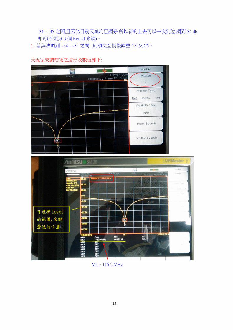
89
-34 ~ -35 之間,且因為目前天線均已調好,所以新的上去可以一次到位,調到-34 db
即可(不須分 3 個 Round 來調)。
5. 若無法調到 -34 ~ -35 之間 ,則須交互慢慢調整 C3 及 C5。
天線完成調校後之波形及數值如下:
Mk1: 115.2 MHz
90
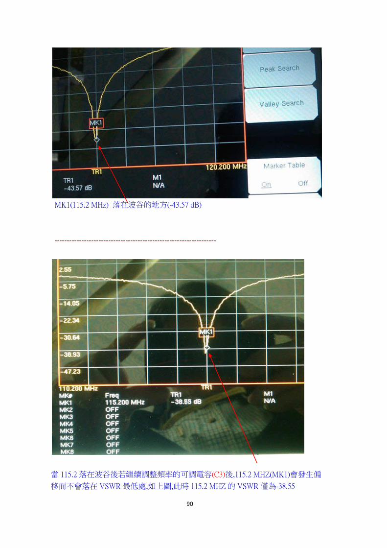
MK1(115.2 MHz) 落在波谷的地方(-43.57 dB)
------------------------------------------------------------------
當 115.2 落在波谷後若繼續調整頻率的可調電容(C3)後,115.2 MHZ(MK1)會發生偏
移而不會落在 VSWR 最低處,如上圖,此時 115.2 MHZ 的 VSWR 僅為-38.55
91
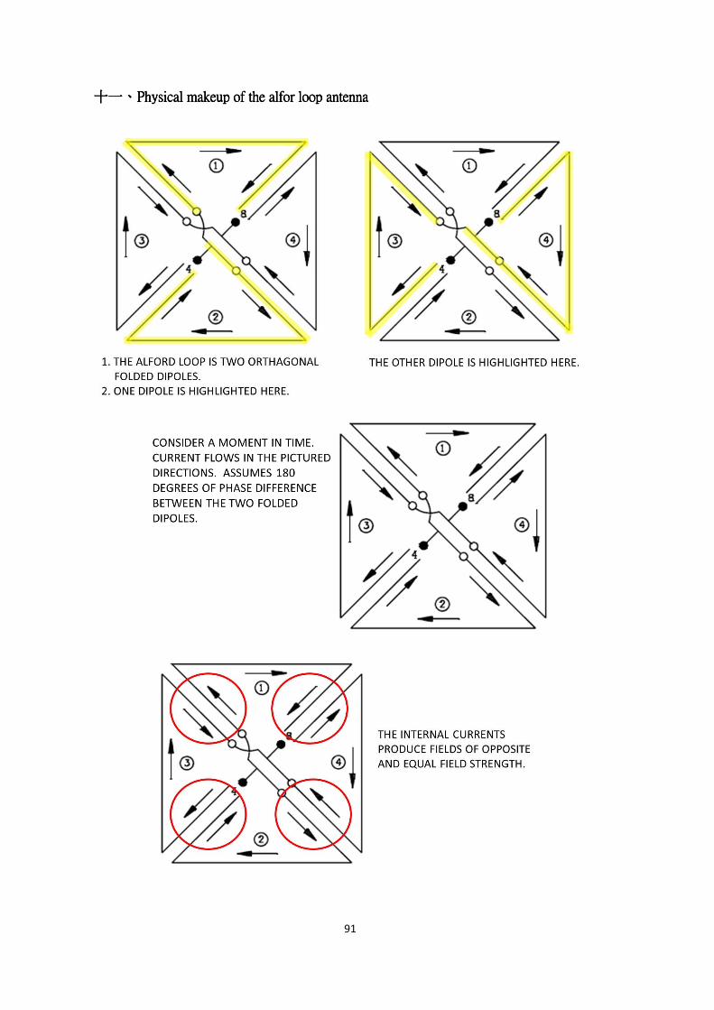
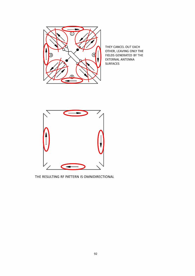
十十十十一一一一、、、、PPPPhysical hysical hysical hysical makeup of the alfor loop antennamakeup of the alfor loop antennamakeup of the alfor loop antennamakeup of the alfor loop antenna
92
93
十二十二十二十二、、、、軟體軟體軟體軟體之之之之 updateupdateupdateupdate 方法方法方法方法
Model 1150A VOR 有三個軟體需要 Upgrade
分別為:
1. RMS software
2. Audio Generator software
3. Monitor software
TOOLS REQUIRED:
SELEX-SI part number 980104-0010, Flash Loader (Included on enclosed CD-ROM).
MATERIALS REQUIRED (以以下軟體版本為例)
1. SELEX-SI part number 978232-0012, RMS Software v5.2.0.2
2. SELEX-SI part number 978239-0009, Audio Generator Software v5.1.0.1
3. SELEX-SI part number 978237-0015, Monitor Software v5.1.0.4
WARNING:
1. Insure System Batteries are charged before beginning procedure to protect
from AC failure.
2. DO NOT remove power or restart equipment until upgrade is fully completed
3. Failure to follow warnings 1 and 2 may result in equipment being inoperable
without factory service.
4. Failure to load the correct software file into a CCA will result in the CCA being
inoperable.
INSTALLING FLASH LOADER:
1. Perform these activities on the PMDT Laptop.
2. Navigate to the SB1150A-0008\980104-0010 Flashloader directory.
3. Double click on setup.exe.
4. Install following the Prompts.
5. Continue on to VOR UPGRADE PROCEDURE.
94
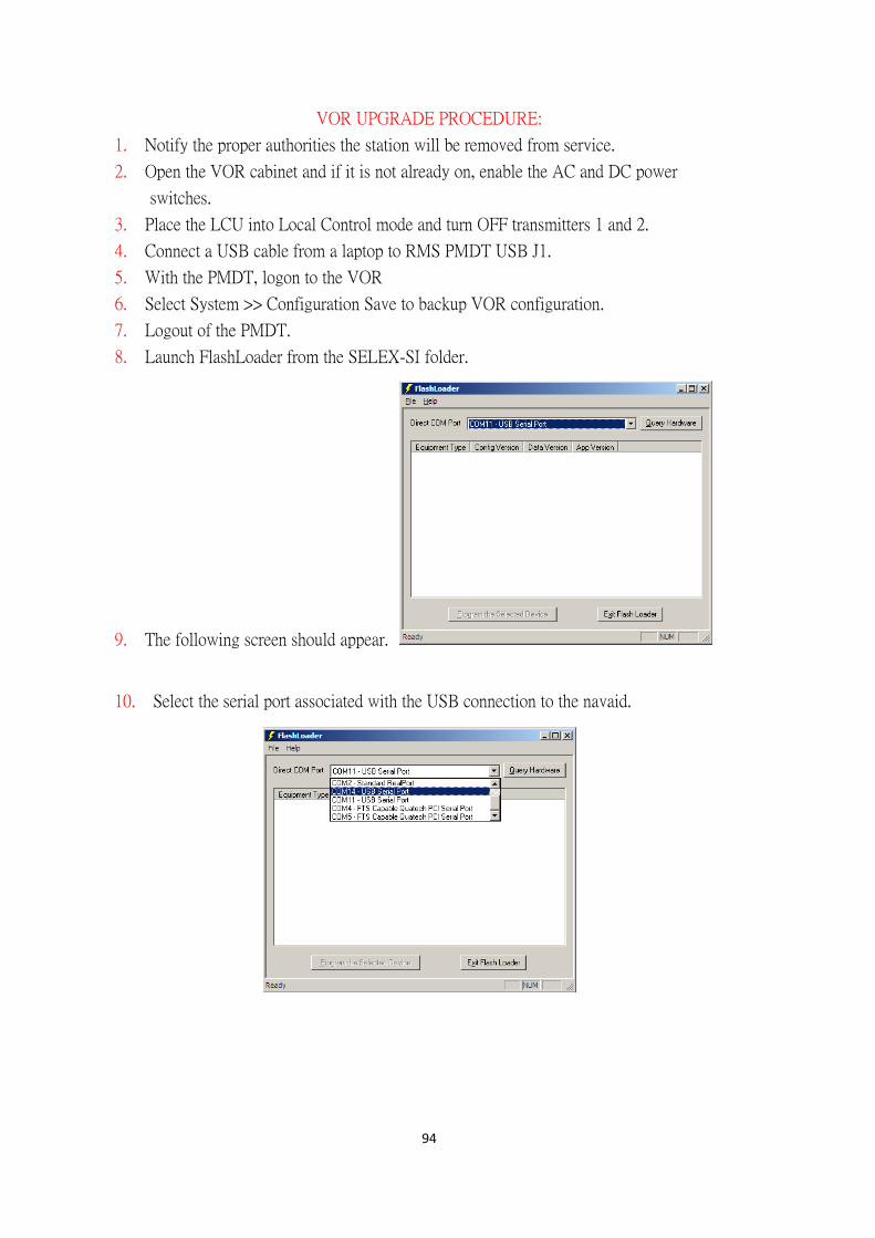
VOR UPGRADE PROCEDURE:
1. Notify the proper authorities the station will be removed from service.
2. Open the VOR cabinet and if it is not already on, enable the AC and DC power
switches.
3. Place the LCU into Local Control mode and turn OFF transmitters 1 and 2.
4. Connect a USB cable from a laptop to RMS PMDT USB J1.
5. With the PMDT, logon to the VOR
6. Select System >> Configuration Save to backup VOR configuration.
7. Logout of the PMDT.
8. Launch FlashLoader from the SELEX-SI folder.
9. The following screen should appear.
10. Select the serial port associated with the USB connection to the navaid.
95
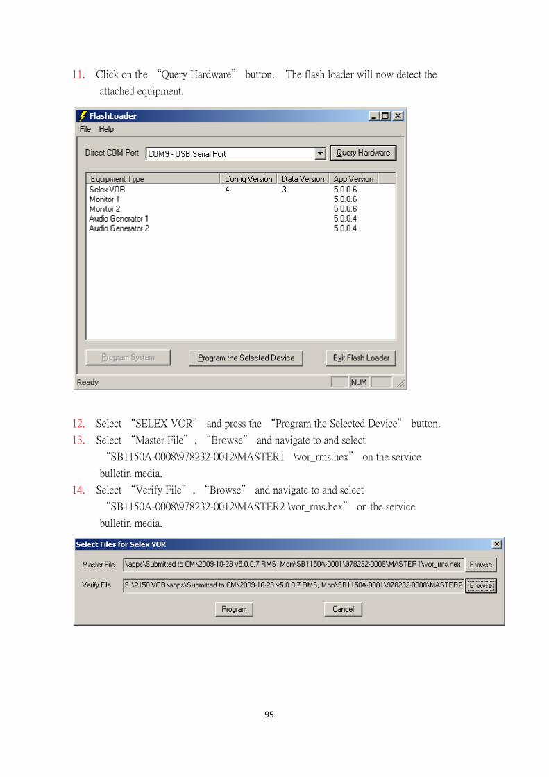
11. Click on the “Query Hardware” button. The flash loader will now detect the
attached equipment.
12. Select “SELEX VOR” and press the “Program the Selected Device” button.
13. Select “Master File”, “Browse” and navigate to and select
“SB1150A-0008\978232-0012\MASTER1 \vor_rms.hex” on the service
bulletin media.
14. Select “Verify File”, “Browse” and navigate to and select
“SB1150A-0008\978232-0012\MASTER2 \vor_rms.hex” on the service
bulletin media.
96
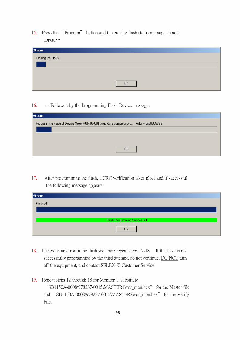
15. Press the “Program” button and the erasing flash status message should
appear…
16. … Followed by the Programming Flash Device message.
17. After programming the flash, a CRC verification takes place and if successful
the following message appears:
18. If there is an error in the flash sequence repeat steps 12-18. If the flash is not
successfully programmed by the third attempt, do not continue. DO NOT turn
off the equipment, and contact SELEX-SI Customer Service.
19. Repeat steps 12 through 18 for Monitor 1, substitute
“SB1150A-0008\978237-0015\MASTER1\vor_mon.hex” for the Master file
and “SB1150A-0008\978237-0015\MASTER2\vor_mon.hex” for the Verify
File.
97
20. Repeat steps 12 through 18 for Monitor 2, substitute
“SB1150A-0008\978237-0015\MASTER1\vor_mon.hex” for the Master file
and “SB1150A-0008\978237-0015\MASTER2\vor_mon.hex” for the Verify
File
21. Repeat steps 12 through 18 for Audio Generator 1, substitute
“SB1150A-0008\978239-0009\MASTER1\vor_ag.hex” for the Master file and
“SB1150A-0001\978239-0009\MASTER2\vor_ag.hex” for the Verify File.
22. Repeat steps 12 through 18 for Audio Generator 2, substitute
“SB1150A-0008\978239-0009\MASTER1\vor_ag.hex” for the Master file and
“SB1150A-0008\978239-0009\MASTER2\vor_ag.hex” for the Verify File.
23. Exit the FlashLoader.
24. Press the LCU Reset button to restart the system.
25. Connect to the VOR with PMDT v8.4.0.4.
26. Place the system in Local Control Mode.
27. Select System >> Configuration Load to reload the VOR configuration.
28. Verify the VOR station returns to normal operation as indicated on the LCU
front panel.
29. Perform a config backup.
30. Place the system in Remote Mode.
31. Close the VOR cabinet and secure.
98
DMEDMEDMEDME
一一一一、、、、DMEDMEDMEDME 概述概述概述概述
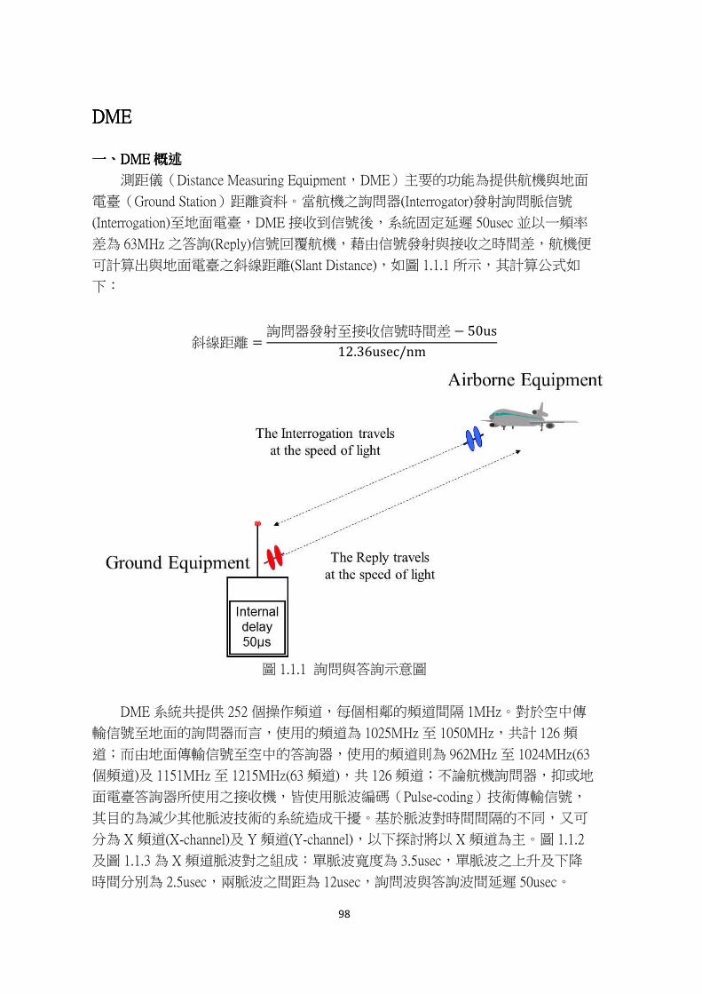
測距儀(Distance Measuring Equipment,DME)主要的功能為提供航機與地面
電臺(Ground Station)距離資料。當航機之詢問器(Interrogator)發射詢問脈信號
(Interrogation)至地面電臺,DME 接收到信號後,系統固定延遲 50usec 並以一頻率
差為 63MHz 之答詢(Reply)信號回覆航機,藉由信號發射與接收之時間差,航機便
可計算出與地面電臺之斜線距離(Slant Distance),如圖 1.1.1 所示,其計算公式如
下:
斜線距離 =詢問器發射至接收信號時間差 − 50us
12.36usec/nm
圖 1.1.1 詢問與答詢示意圖
DME 系統共提供 252 個操作頻道,每個相鄰的頻道間隔 1MHz。對於空中傳
輸信號至地面的詢問器而言,使用的頻道為 1025MHz 至 1050MHz,共計 126 頻
道;而由地面傳輸信號至空中的答詢器,使用的頻道則為 962MHz 至 1024MHz(63
個頻道)及 1151MHz 至 1215MHz(63 頻道),共 126 頻道;不論航機詢問器,抑或地
面電臺答詢器所使用之接收機,皆使用脈波編碼(Pulse-coding)技術傳輸信號,
其目的為減少其他脈波技術的系統造成干擾。基於脈波對時間間隔的不同,又可
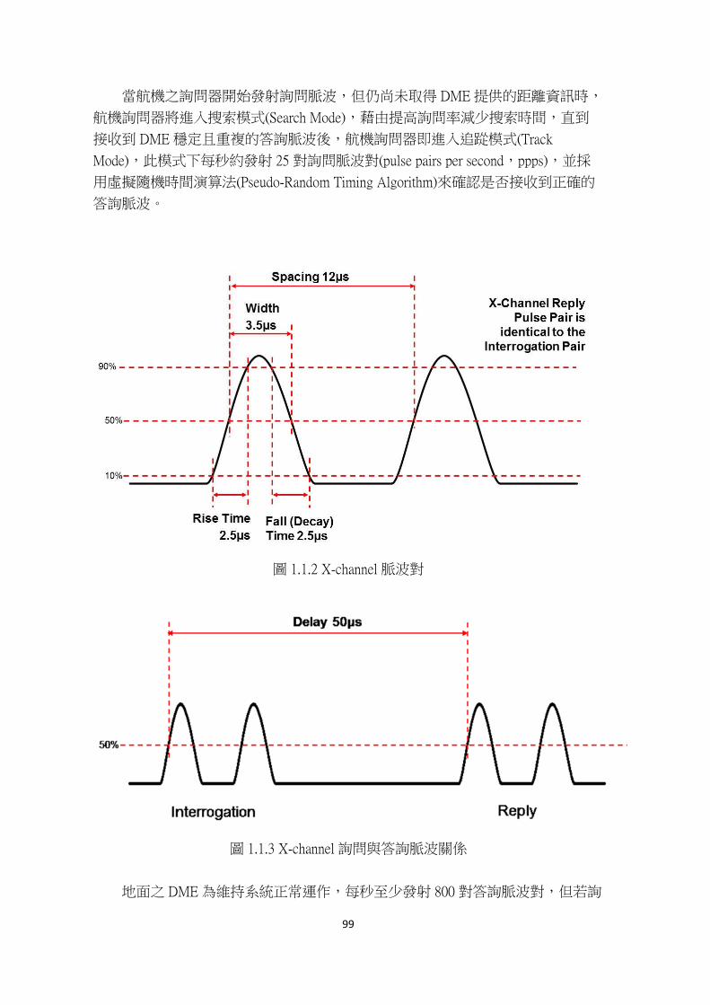
分為 X 頻道(X-channel)及 Y 頻道(Y-channel),以下探討將以 X 頻道為主。圖 1.1.2
及圖 1.1.3 為 X 頻道脈波對之組成:單脈波寬度為 3.5usec,單脈波之上升及下降
時間分別為 2.5usec,兩脈波之間距為 12usec,詢問波與答詢波間延遲 50usec。
99
當航機之詢問器開始發射詢問脈波,但仍尚未取得 DME 提供的距離資訊時,
航機詢問器將進入搜索模式(Search Mode),藉由提高詢問率減少搜索時間,直到
接收到 DME 穩定且重複的答詢脈波後,航機詢問器即進入追踨模式(Track
Mode),此模式下每秒約發射 25 對詢問脈波對(pulse pairs per second,ppps),並採
用虛擬隨機時間演算法(Pseudo-Random Timing Algorithm)來確認是否接收到正確的
答詢脈波。
圖 1.1.2 X-channel 脈波對
圖 1.1.3 X-channel 詢問與答詢脈波關係
地面之 DME 為維持系統正常運作,每秒至少發射 800 對答詢脈波對,但若詢
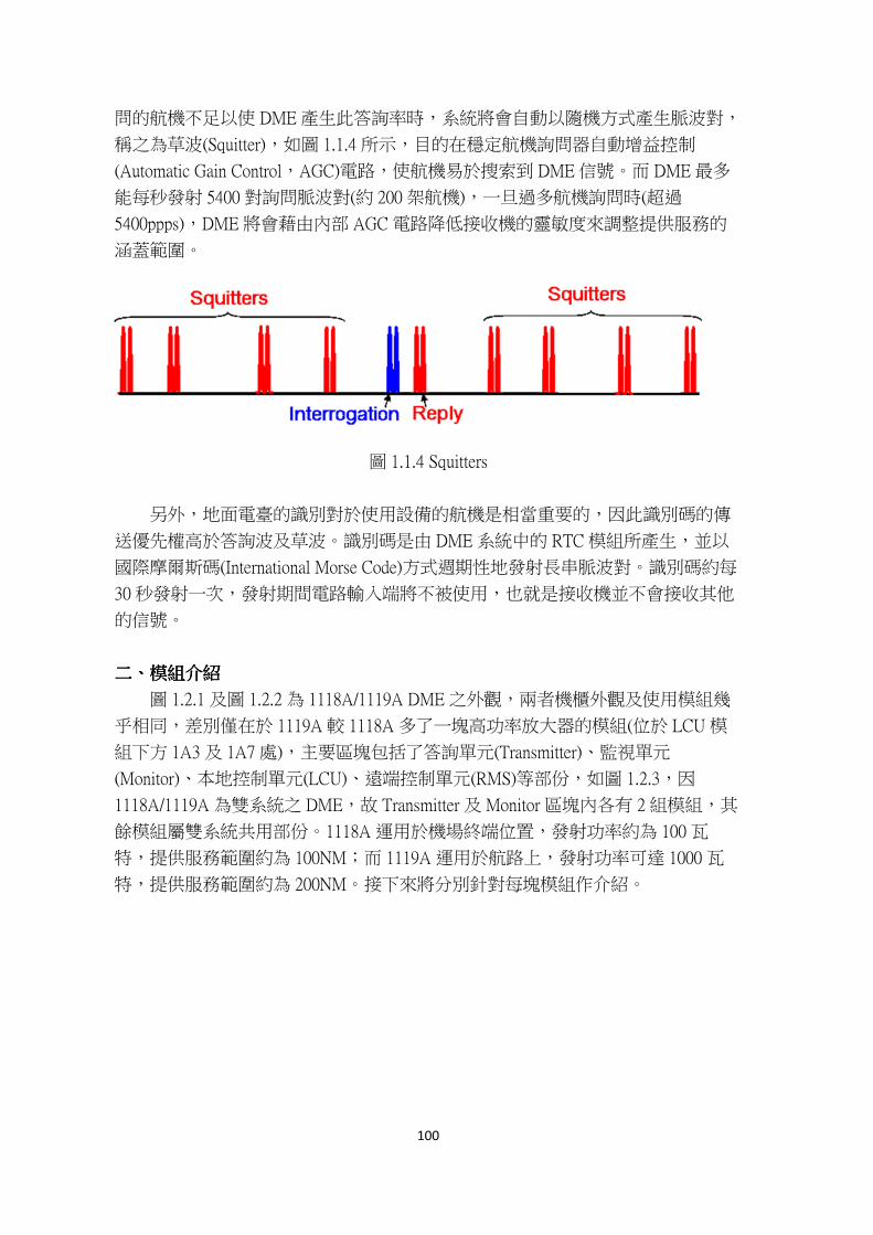
100
問的航機不足以使 DME 產生此答詢率時,系統將會自動以隨機方式產生脈波對,
稱之為草波(Squitter),如圖 1.1.4 所示,目的在穩定航機詢問器自動增益控制
(Automatic Gain Control,AGC)電路,使航機易於搜索到 DME 信號。而 DME 最多
能每秒發射 5400 對詢問脈波對(約 200 架航機),一旦過多航機詢問時(超過
5400ppps),DME 將會藉由內部 AGC 電路降低接收機的靈敏度來調整提供服務的
涵蓋範圍。
圖 1.1.4 Squitters
另外,地面電臺的識別對於使用設備的航機是相當重要的,因此識別碼的傳
送優先權高於答詢波及草波。識別碼是由 DME 系統中的 RTC 模組所產生,並以
國際摩爾斯碼(International Morse Code)方式週期性地發射長串脈波對。識別碼約每
30 秒發射一次,發射期間電路輸入端將不被使用,也就是接收機並不會接收其他
的信號。
二二二二、、、、模組模組模組模組介紹介紹介紹介紹
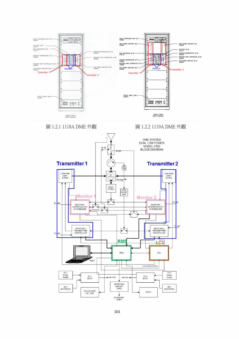
圖 1.2.1 及圖 1.2.2 為 1118A/1119A DME 之外觀,兩者機櫃外觀及使用模組幾
乎相同,差別僅在於 1119A 較 1118A 多了一塊高功率放大器的模組(位於 LCU 模
組下方 1A3 及 1A7 處),主要區塊包括了答詢單元(Transmitter)、監視單元
(Monitor)、本地控制單元(LCU)、遠端控制單元(RMS)等部份,如圖 1.2.3,因
1118A/1119A 為雙系統之 DME,故 Transmitter 及 Monitor 區塊內各有 2 組模組,其
餘模組屬雙系統共用部份。1118A 運用於機場終端位置,發射功率約為 100 瓦
特,提供服務範圍約為 100NM;而 1119A 運用於航路上,發射功率可達 1000 瓦
特,提供服務範圍約為 200NM。接下來將分別針對每塊模組作介紹。
101
圖 1.2.1 1118A DME 外觀 圖 1.2.2 1119A DME 外觀
102
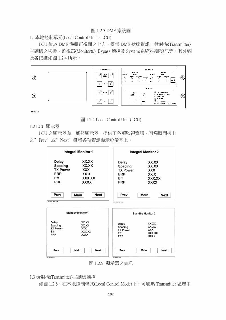
圖 1.2.3 DME 系統圖
1. 本地控制單元(Local Control Unit,LCU)
LCU 位於 DME 機櫃正視面之上方,提供 DME 狀態資訊、發射機(Transmitter)
主副機之切換、監視器(Monitor)的 Bypass 選擇及 System(系統)告警資訊等,其外觀
及各按鍵如圖 1.2.4 所示。
圖 1.2.4 Local Control Unit (LCU)
1.2 LCU 顯示器
LCU 之顯示器為一觸控顯示器,提供了各項監視資訊,可觸壓面板上
之”Prev”或”Next”鍵將各項資訊顯示於螢幕上。
圖 1.2.5 顯示器之資訊
1.3 發射機(Transmitter)主副機選擇
如圖 1.2.6,在本地控制模式(Local Control Mode)下,可觸壓 Transmitter 區塊中
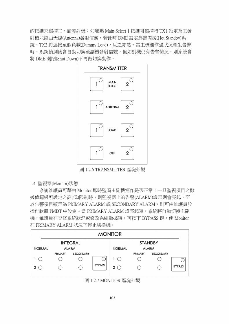
103
的按鍵來選擇主、副發射機;如觸壓 Main Select 1 按鍵可選擇將 TX1 設定為主發
射機並經由天線(Antenna)發射信號,若此時 DME 設定為熱備援(Hot Standby)系
統,TX2 將連接至假負載(Dummy Load),反之亦然。當主機運作遇狀況產生告警
時,系統偵測後會自動切換至副機發射信號,但如副機仍有告警情況,則系統會
將 DME 關閉(Shut Down)不再做切換動作。
圖 1.2.6 TRANSMITTER 區塊外觀
1.4 監視器(Monitor)狀態
系統維護員可藉由 Monitor 即時監看主副機運作是否正常;一旦監視項目之數
據值超過所設定之高(低)限制時,則監視器上的告警(ALARM)燈示則會亮起,至
於告警項目顯示為 PRIMARY ALARM 或 SECONDARY ALARM,則可由維護員於
操作軟體 PMDT 中設定。當 PRIMARY ALARM 燈亮起時,系統將自動切換主副
機,維護員在查修系統狀況或修改系統數據時,可按下 BYPASS 鍵,使 Monitor
在 PRIMARY ALARM 狀況下停止切換機。
圖 1.2.7 MONITOR 區塊外觀
104
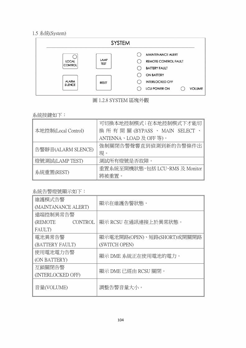
1.5 系統(System)
圖 1.2.8 SYSTEM 區塊外觀
系統按鍵如下:
本地控制(Local Control)
可切換本地控制模式;在本地控制模式下才能切
換 所 有 開 關 (BYPASS 、 MAIN SELECT 、
ANTENNA、LOAD 及 OFF 等)。
告警靜音(ALARM SLENCE) 強制關閉告警聲響直到偵測到新的告警條件出
現。
燈號測試(LAMP TEST) 測試所有燈號是否故障。
系統重置(REST) 重置系統至開機狀態,包括 LCU、RMS 及 Monitor
將被重置。
系統告警燈號顯示如下:
維護模式告警
(MAINTANANCE ALERT) 顯示在維護告警狀態。
遠端控制異常告警
(REMOTE CONTROL
FAULT)
顯示 RCSU 在通訊連接上於異常狀態。
電池異常告警
(BATTERY FAULT)
顯示電池開路(OPEN)、短路(SHORT)或開關開路
(SWITCH OPEN)
使用電池電力告警
(ON BATTERY) 顯示 DME 系統正在使用電池的電力。
互鎖關閉告警
(INTERLOCKED OFF) 顯示 DME 已經由 RCSU 關閉。
音量(VOLUME) 調整告警音量大小。
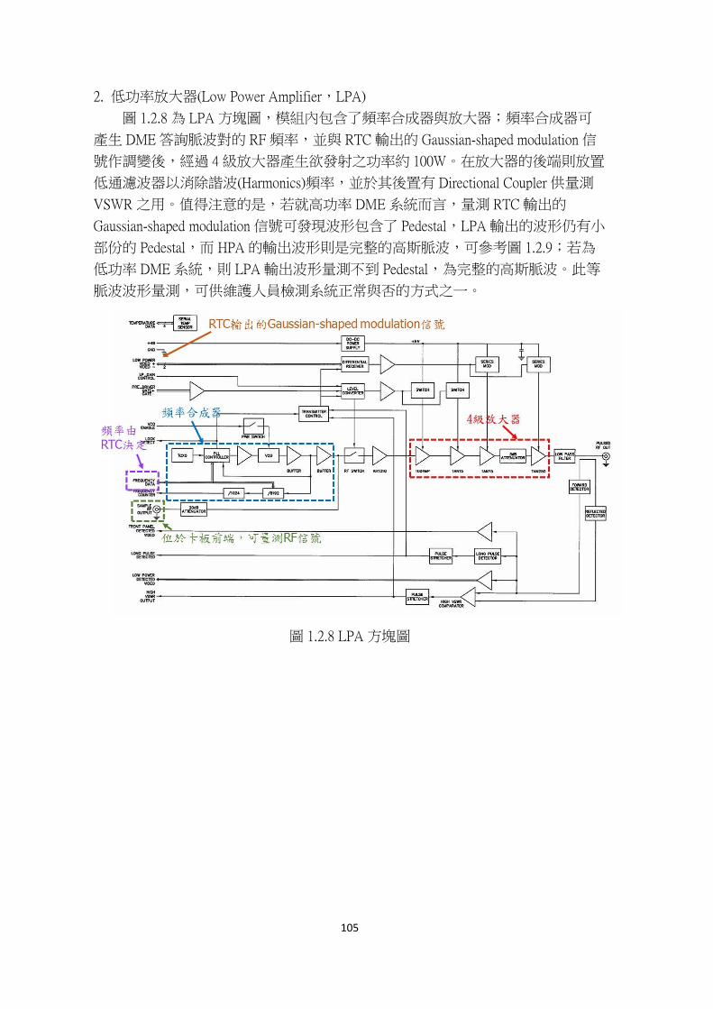
105
2. 低功率放大器(Low Power Amplifier,LPA)
圖 1.2.8 為 LPA 方塊圖,模組內包含了頻率合成器與放大器;頻率合成器可
產生 DME 答詢脈波對的 RF 頻率,並與 RTC 輸出的 Gaussian-shaped modulation 信
號作調變後,經過 4 級放大器產生欲發射之功率約 100W。在放大器的後端則放置
低通濾波器以消除諧波(Harmonics)頻率,並於其後置有 Directional Coupler 供量測
VSWR 之用。值得注意的是,若就高功率 DME 系統而言,量測 RTC 輸出的
Gaussian-shaped modulation 信號可發現波形包含了 Pedestal,LPA 輸出的波形仍有小
部份的 Pedestal,而 HPA 的輸出波形則是完整的高斯脈波,可參考圖 1.2.9;若為
低功率 DME 系統,則 LPA 輸出波形量測不到 Pedestal,為完整的高斯脈波。此等
脈波波形量測,可供維護人員檢測系統正常與否的方式之一。
圖 1.2.8 LPA 方塊圖
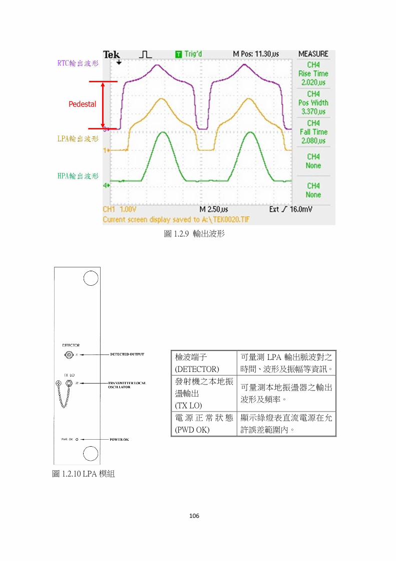
106
圖 1.2.9 輸出波形
圖 1.2.10 LPA 模組
檢波端子
(DETECTOR)
可量測 LPA 輸出脈波對之
時間、波形及振幅等資訊。
發射機之本地振
盪輸出
(TX LO)
可量測本地振盪器之輸出
波形及頻率。
電 源 正 常 狀 態
(PWD OK)
顯示綠燈表直流電源在允
許誤差範圍內。
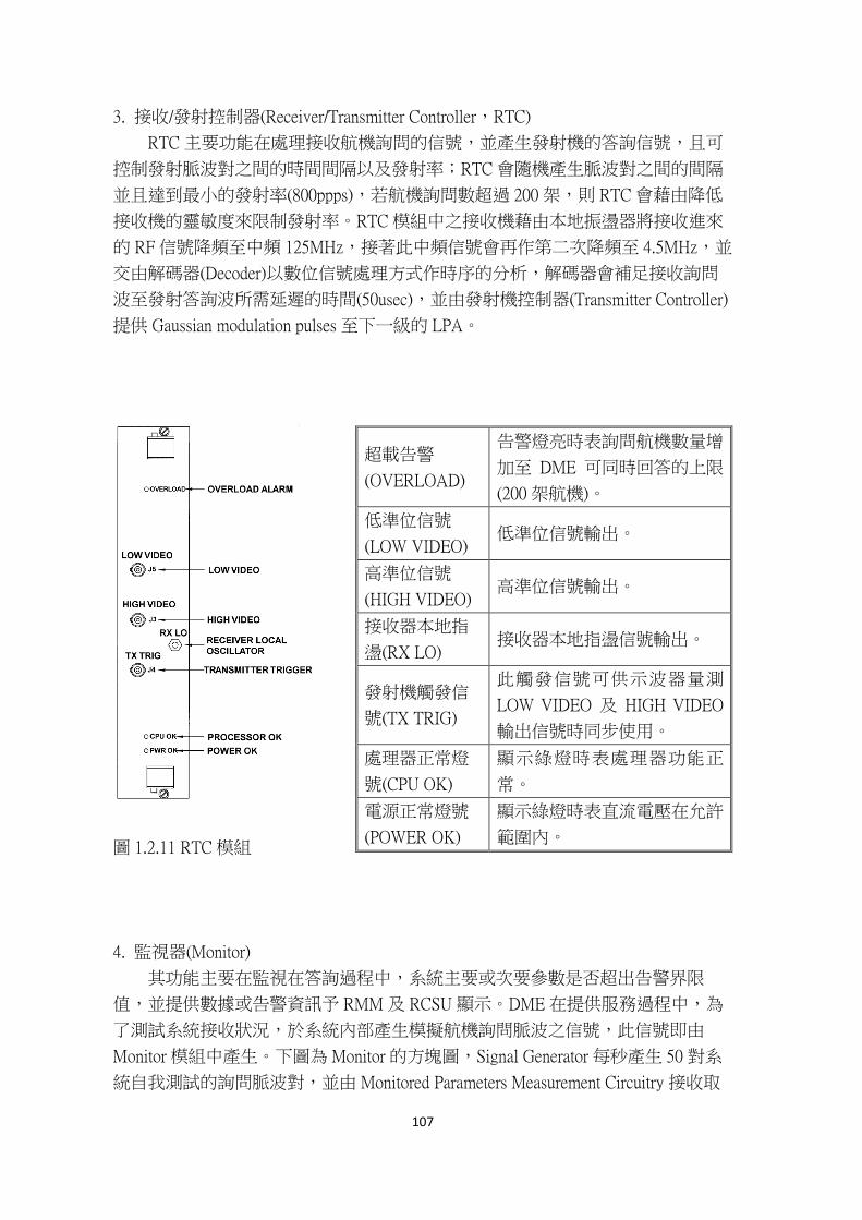
107
3. 接收/發射控制器(Receiver/Transmitter Controller,RTC)
RTC 主要功能在處理接收航機詢問的信號,並產生發射機的答詢信號,且可
控制發射脈波對之間的時間間隔以及發射率;RTC 會隨機產生脈波對之間的間隔
並且達到最小的發射率(800ppps),若航機詢問數超過 200 架,則 RTC 會藉由降低
接收機的靈敏度來限制發射率。RTC 模組中之接收機藉由本地振盪器將接收進來
的 RF 信號降頻至中頻 125MHz,接著此中頻信號會再作第二次降頻至 4.5MHz,並
交由解碼器(Decoder)以數位信號處理方式作時序的分析,解碼器會補足接收詢問
波至發射答詢波所需延遲的時間(50usec),並由發射機控制器(Transmitter Controller)
提供 Gaussian modulation pulses 至下一級的 LPA。
圖 1.2.11 RTC 模組
4. 監視器(Monitor)
其功能主要在監視在答詢過程中,系統主要或次要參數是否超出告警界限
值,並提供數據或告警資訊予 RMM 及 RCSU 顯示。DME 在提供服務過程中,為
了測試系統接收狀況,於系統內部產生模擬航機詢問脈波之信號,此信號即由
Monitor 模組中產生。下圖為 Monitor 的方塊圖,Signal Generator 每秒產生 50 對系
統自我測試的詢問脈波對,並由 Monitored Parameters Measurement Circuitry 接收取
超載告警
(OVERLOAD)
告警燈亮時表詢問航機數量增
加至 DME 可同時回答的上限
(200 架航機)。
低準位信號
(LOW VIDEO) 低準位信號輸出。
高準位信號
(HIGH VIDEO) 高準位信號輸出。
接收器本地指
盪(RX LO) 接收器本地指盪信號輸出。
發射機觸發信
號(TX TRIG)
此觸發信號可供示波器量測
LOW VIDEO 及 HIGH VIDEO
輸出信號時同步使用。
處理器正常燈
號(CPU OK)
顯示綠燈時表處理器功能正
常。
電源正常燈號
(POWER OK)
顯示綠燈時表直流電壓在允許
範圍內。
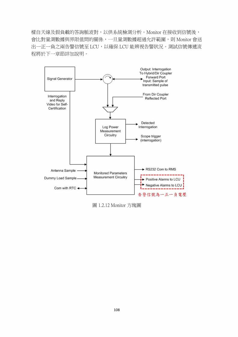
108
樣自天線及假負載的答詢脈波對,以供系統檢測分析。Monitor 在接收到信號後,
會比對量測數據與界限值間的關係,一旦量測數據超過允許範圍,則 Monitor 會送
出一正一負之兩告警信號至 LCU,以確保 LCU 能辨視告警狀況。測試信號傳遞流
程將於下一章節詳加說明。
圖 1.2.12 Monitor 方塊圖
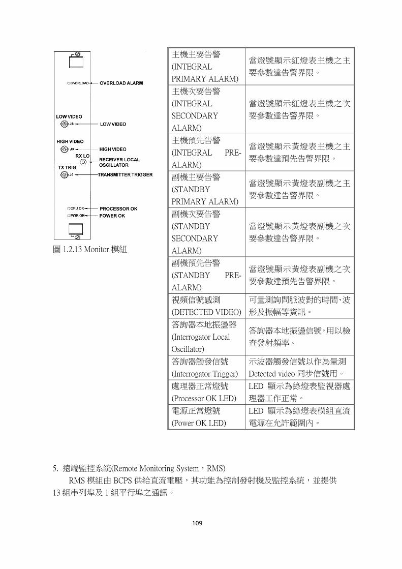
109
圖 1.2.13 Monitor 模組
5. 遠端監控系統(Remote Monitoring System,RMS)
RMS 模組由 BCPS 供給直流電壓,其功能為控制發射機及監控系統,並提供
13 組串列埠及 1 組平行埠之通訊。
主機主要告警
(INTEGRAL
PRIMARY ALARM)
當燈號顯示紅燈表主機之主
要參數達告警界限。
主機次要告警
(INTEGRAL
SECONDARY
ALARM)
當燈號顯示紅燈表主機之次
要參數達告警界限。
主機預先告警
(INTEGRAL PRE-
ALARM)
當燈號顯示黃燈表主機之主
要參數達預先告警界限。
副機主要告警
(STANDBY
PRIMARY ALARM)
當燈號顯示黃燈表副機之主
要參數達告警界限。
副機次要告警
(STANDBY
SECONDARY
ALARM)
當燈號顯示黃燈表副機之次
要參數達告警界限。
副機預先告警
(STANDBY PRE-
ALARM)
當燈號顯示黃燈表副機之次
要參數達預先告警界限。
視頻信號感測
(DETECTED VIDEO)
可量測詢問脈波對的時間、波
形及振幅等資訊。
答詢器本地振盪器
(Interrogator Local
Oscillator)
答詢器本地振盪信號,用以檢
查發射頻率。
答詢器觸發信號
(Interrogator Trigger)
示波器觸發信號以作為量測
Detected video 同步信號用。
處理器正常燈號
(Processor OK LED)
LED 顯示為綠燈表監視器處
理器工作正常。
電源正常燈號
(Power OK LED)
LED 顯示為綠燈表模組直流
電源在允許範圍內。
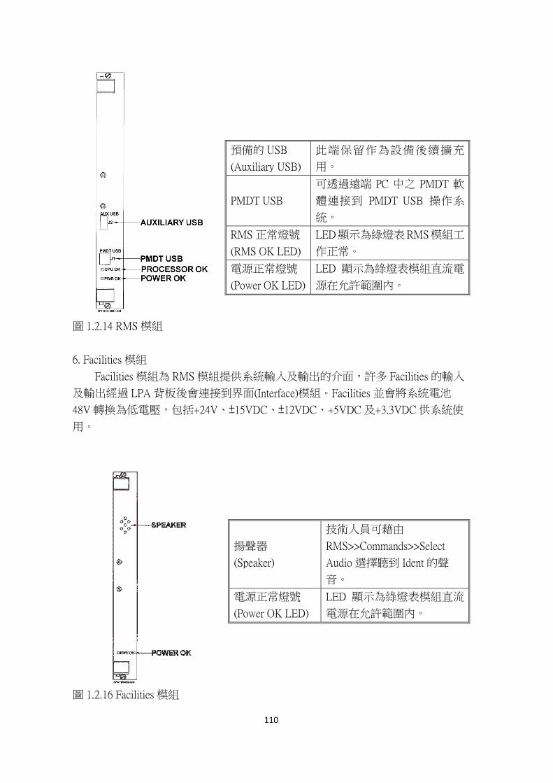
110
圖 1.2.14 RMS 模組
6. Facilities 模組
Facilities 模組為 RMS 模組提供系統輸入及輸出的介面,許多 Facilities 的輸入
及輸出經過 LPA 背板後會連接到界面(Interface)模組。Facilities 並會將系統電池
48V 轉換為低電壓,包括+24V、±15VDC、±12VDC、+5VDC 及+3.3VDC 供系統使
用。
圖 1.2.16 Facilities 模組
預備的 USB
(Auxiliary USB)
此端保留作為設備後續擴充
用。
PMDT USB
可透過遠端 PC 中之 PMDT 軟
體連接到 PMDT USB 操作系
統。
RMS 正常燈號
(RMS OK LED)
LED 顯示為綠燈表 RMS 模組工
作正常。
電源正常燈號
(Power OK LED)
LED 顯示為綠燈表模組直流電
源在允許範圍內。
揚聲器
(Speaker)
技術人員可藉由
RMS>>Commands>>Select
Audio 選擇聽到 Ident 的聲
音。
電源正常燈號
(Power OK LED)
LED 顯示為綠燈表模組直流
電源在允許範圍內。
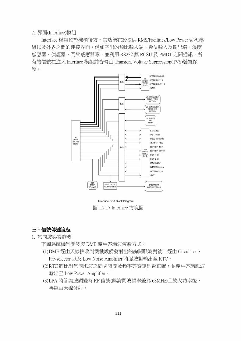
111
7. 界面(Interface)模組
Interface 模組位於機櫃後方,其功能在於提供 RMS/Facilities/Low Power 背板模
組以及外界之間的連接界面,例如空出的類比輸入端、數位輸入及輸出端、溫度
感應器、偵煙器、門禁感應器等,並利用 RS232 與 RCSU 及 PMDT 之間通訊,所
有的信號在進入 Interface 模組前皆會由 Transient Voltage Suppression(TVS)裝置保
護。
圖 1.2.17 Interface 方塊圖
三三三三、、、、信號傳信號傳信號傳信號傳遞遞遞遞流程流程流程流程
1. 詢問波與答詢波
下圖為航機詢問波與 DME 產生答詢波傳輸方式:
(1) DME 經由天線接收到機載設備發射出的詢問脈波對後,經由 Circulator、
Pre-selector 以及 Low Noise Amplifier 將脈波對輸出至 RTC。
(2) RTC 將比對詢問脈波之間隔時間及頻率等資訊是否正確,並產生答詢脈波
輸出至 Low Power Amplifier。
(3) LPA 將答詢波調變為 RF 信號(與詢問波頻率差為 63MHz)且放大功率後,
再經由天線發射。
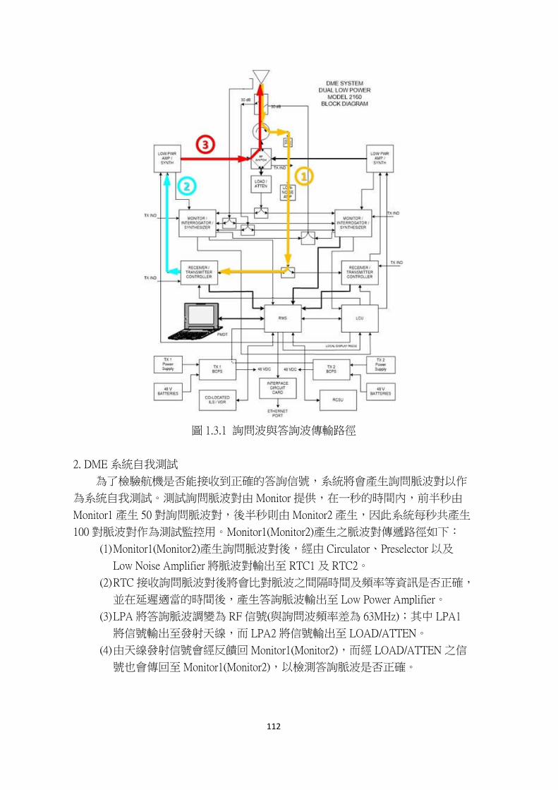
112
圖 1.3.1 詢問波與答詢波傳輸路徑
2. DME 系統自我測試
為了檢驗航機是否能接收到正確的答詢信號,系統將會產生詢問脈波對以作
為系統自我測試。測試詢問脈波對由 Monitor 提供,在一秒的時間內,前半秒由
Monitor1 產生 50 對詢問脈波對,後半秒則由 Monitor2 產生,因此系統每秒共產生
100 對脈波對作為測試監控用。Monitor1(Monitor2)產生之脈波對傳遞路徑如下:
(1) Monitor1(Monitor2)產生詢問脈波對後,經由 Circulator、Preselector 以及
Low Noise Amplifier 將脈波對輸出至 RTC1 及 RTC2。
(2) RTC 接收詢問脈波對後將會比對脈波之間隔時間及頻率等資訊是否正確,
並在延遲適當的時間後,產生答詢脈波輸出至 Low Power Amplifier。
(3) LPA 將答詢脈波調變為 RF 信號(與詢問波頻率差為 63MHz);其中 LPA1
將信號輸出至發射天線,而 LPA2 將信號輸出至 LOAD/ATTEN。
(4) 由天線發射信號會經反饋回 Monitor1(Monitor2),而經 LOAD/ATTEN 之信
號也會傳回至 Monitor1(Monitor2),以檢測答詢脈波是否正確。
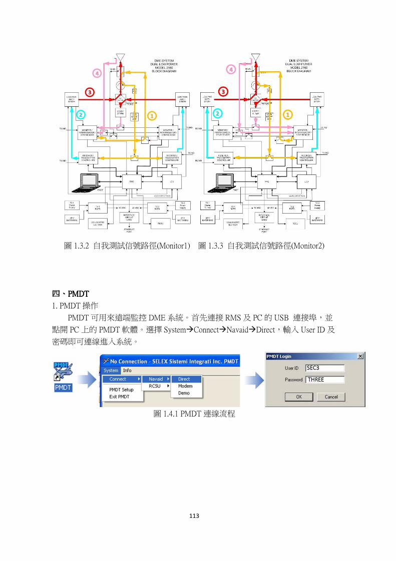
113
圖 1.3.2 自我測試信號路徑(Monitor1) 圖 1.3.3 自我測試信號路徑(Monitor2)
四四四四、、、、PMDTPMDTPMDTPMDT
1. PMDT 操作
PMDT 可用來遠端監控 DME 系統。首先連接 RMS 及 PC 的 USB 連接埠,並
點開 PC 上的 PMDT 軟體。選擇 System�Connect�Navaid�Direct,輸入 User ID 及
密碼即可連線進入系統。
圖 1.4.1 PMDT 連線流程
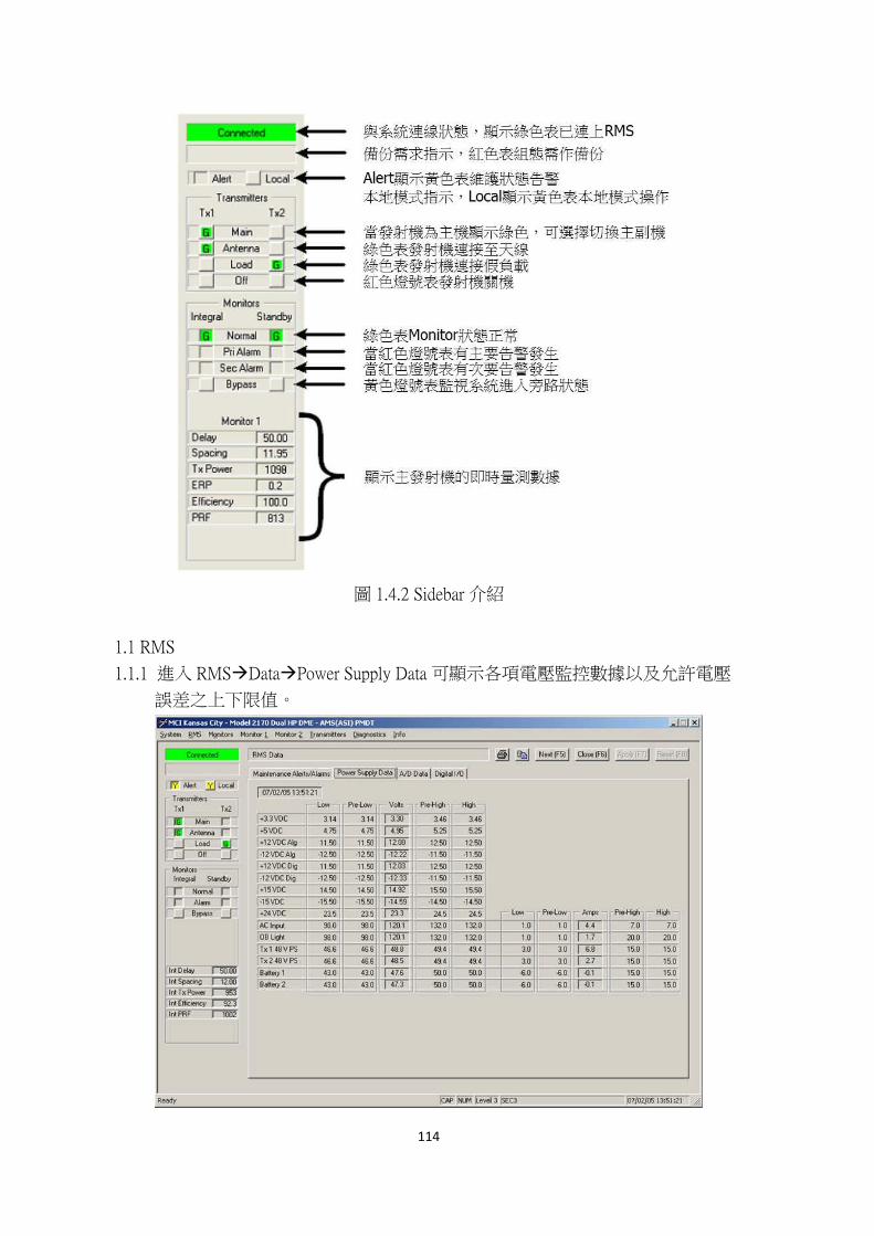
114
圖 1.4.2 Sidebar 介紹
1.1 RMS
1.1.1 進入 RMS�Data�Power Supply Data 可顯示各項電壓監控數據以及允許電壓
誤差之上下限值。
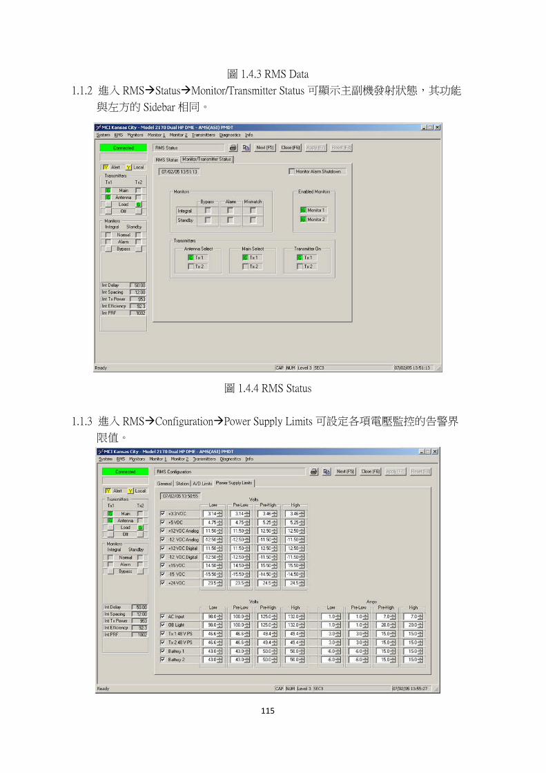
115
圖 1.4.3 RMS Data
1.1.2 進入 RMS�Status�Monitor/Transmitter Status 可顯示主副機發射狀態,其功能
與左方的 Sidebar 相同。
圖 1.4.4 RMS Status
1.1.3 進入 RMS�Configuration�Power Supply Limits 可設定各項電壓監控的告警界
限值。
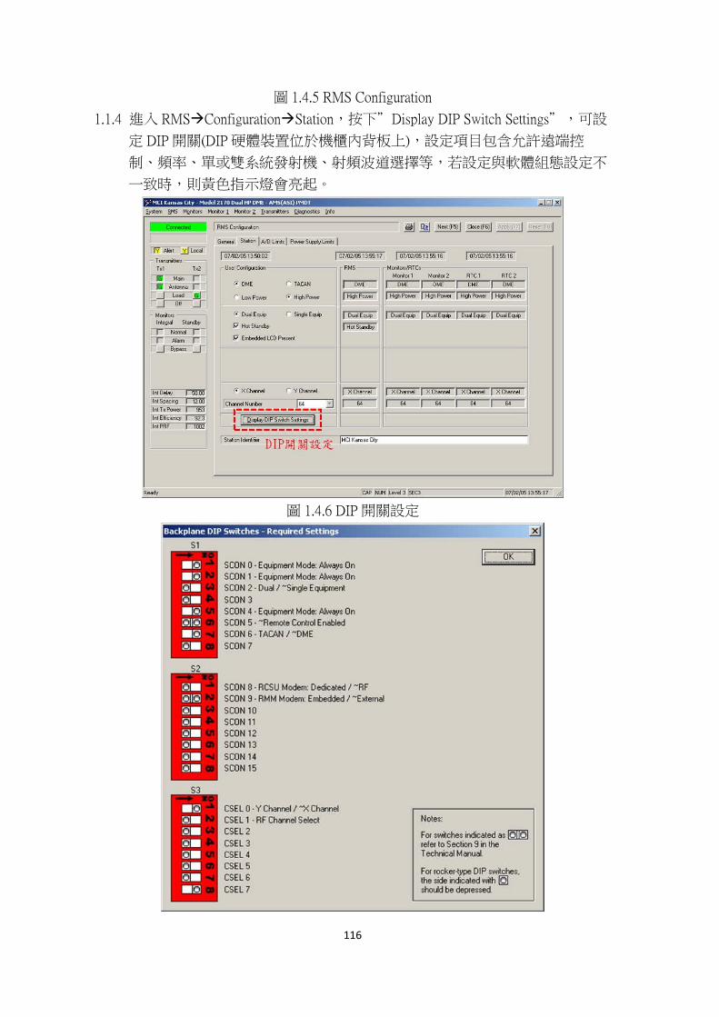
116
圖 1.4.5 RMS Configuration
1.1.4 進入 RMS�Configuration�Station,按下”Display DIP Switch Settings”,可設
定 DIP 開關(DIP 硬體裝置位於機櫃內背板上),設定項目包含允許遠端控
制、頻率、單或雙系統發射機、射頻波道選擇等,若設定與軟體組態設定不
一致時,則黃色指示燈會亮起。
圖 1.4.6 DIP 開關設定
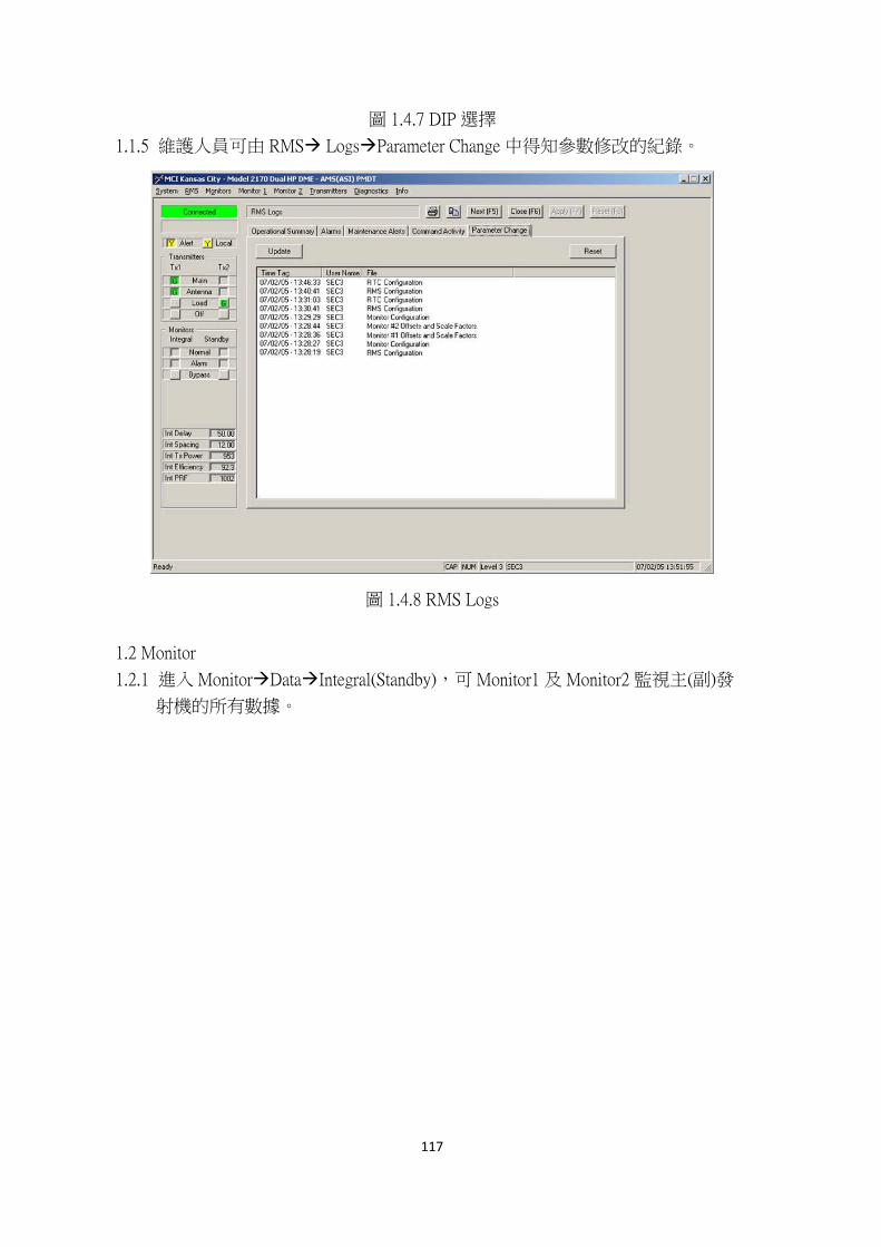
117
圖 1.4.7 DIP 選擇
1.1.5 維護人員可由 RMS� Logs�Parameter Change 中得知參數修改的紀錄。
圖 1.4.8 RMS Logs
1.2 Monitor
1.2.1 進入 Monitor�Data�Integral(Standby),可 Monitor1 及 Monitor2 監視主(副)發
射機的所有數據。
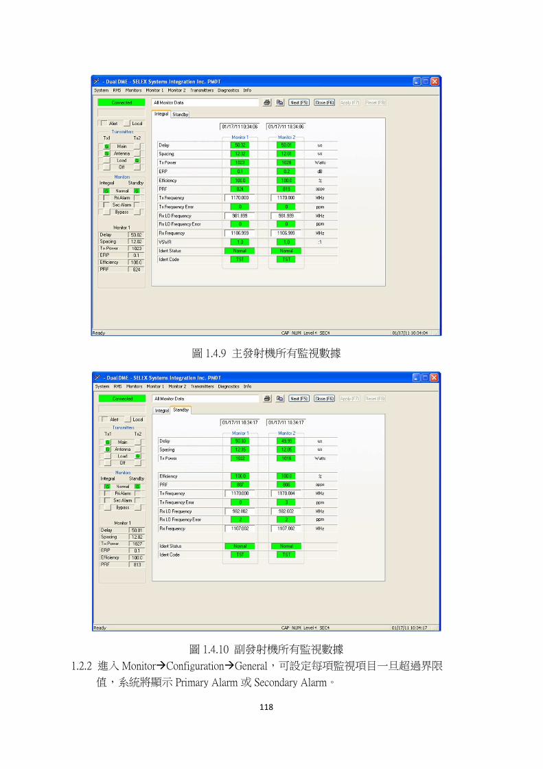
118
圖 1.4.9 主發射機所有監視數據
圖 1.4.10 副發射機所有監視數據
1.2.2 進入 Monitor�Configuration�General,可設定每項監視項目一旦超過界限
值,系統將顯示 Primary Alarm 或 Secondary Alarm。
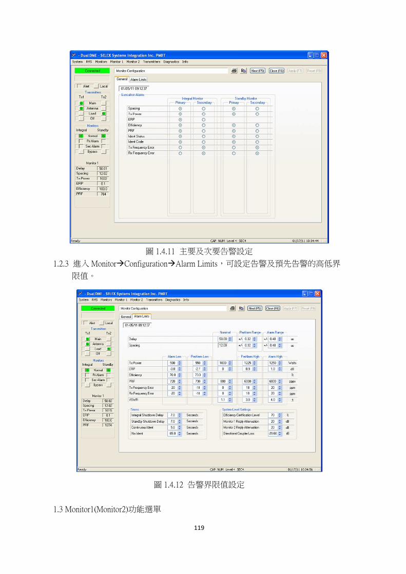
119
圖 1.4.11 主要及次要告警設定
1.2.3 進入 Monitor�Configuration�Alarm Limits,可設定告警及預先告警的高低界
限值。
圖 1.4.12 告警界限值設定
1.3 Monitor1(Monitor2)功能選單
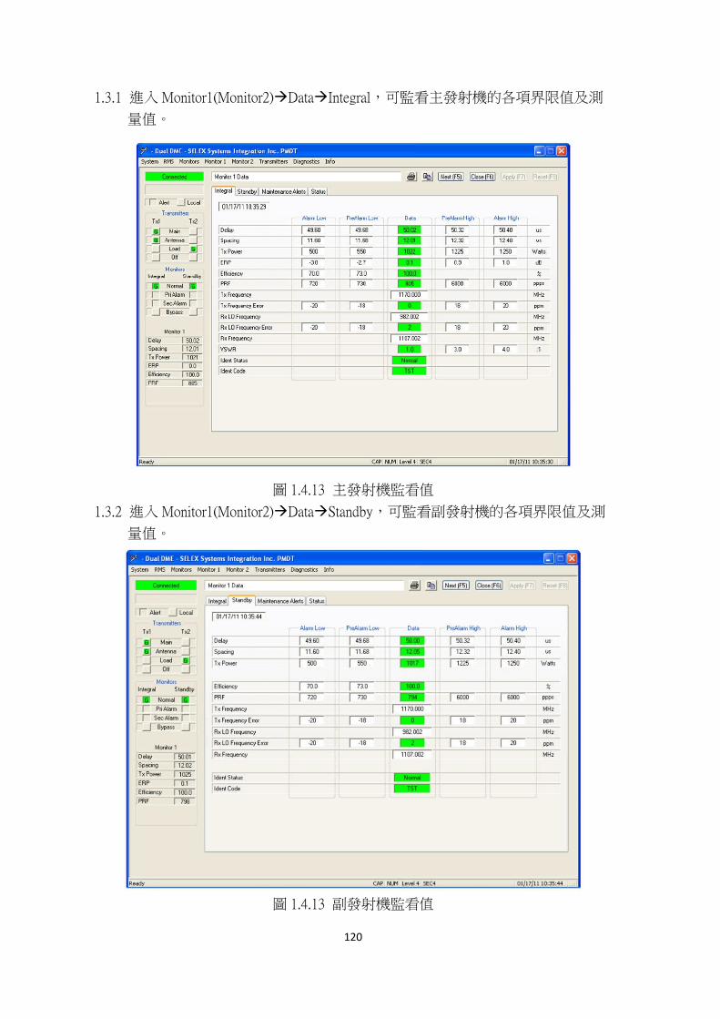
120
1.3.1 進入 Monitor1(Monitor2)�Data�Integral,可監看主發射機的各項界限值及測
量值。
圖 1.4.13 主發射機監看值
1.3.2 進入 Monitor1(Monitor2)�Data�Standby,可監看副發射機的各項界限值及測
量值。
圖 1.4.13 副發射機監看值
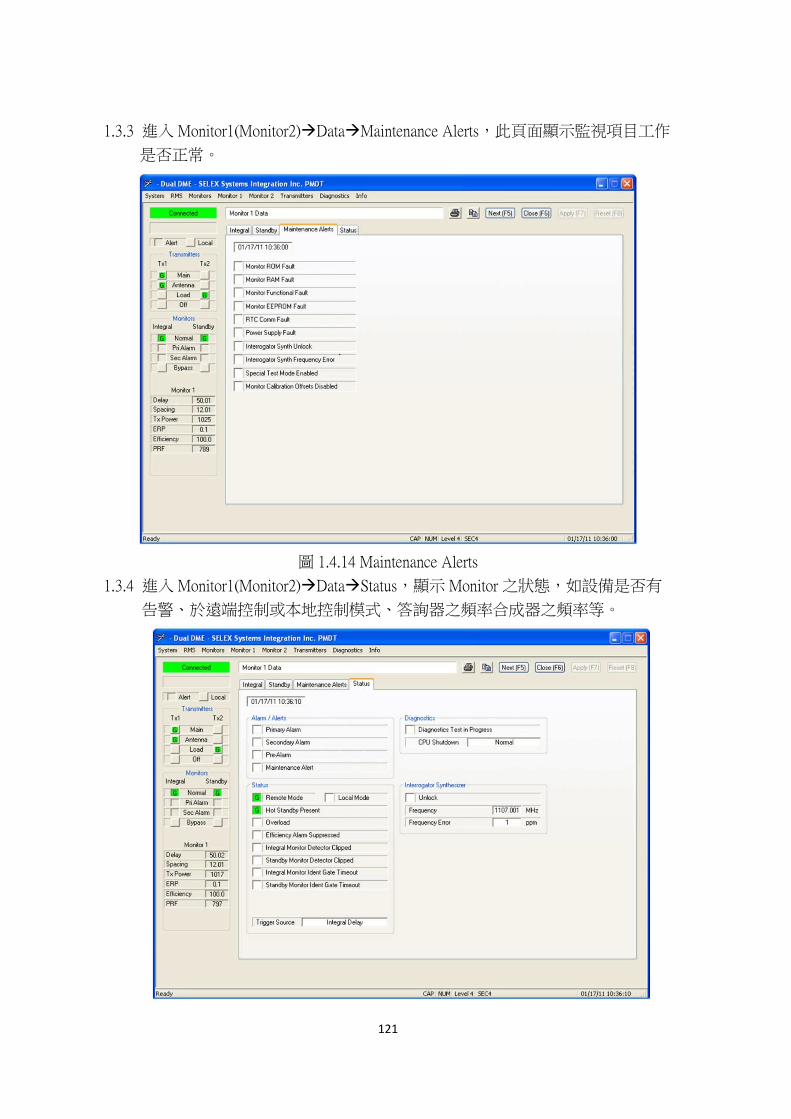
121
1.3.3 進入 Monitor1(Monitor2)�Data�Maintenance Alerts,此頁面顯示監視項目工作
是否正常。
圖 1.4.14 Maintenance Alerts
1.3.4 進入 Monitor1(Monitor2)�Data�Status,顯示 Monitor 之狀態,如設備是否有
告警、於遠端控制或本地控制模式、答詢器之頻率合成器之頻率等。
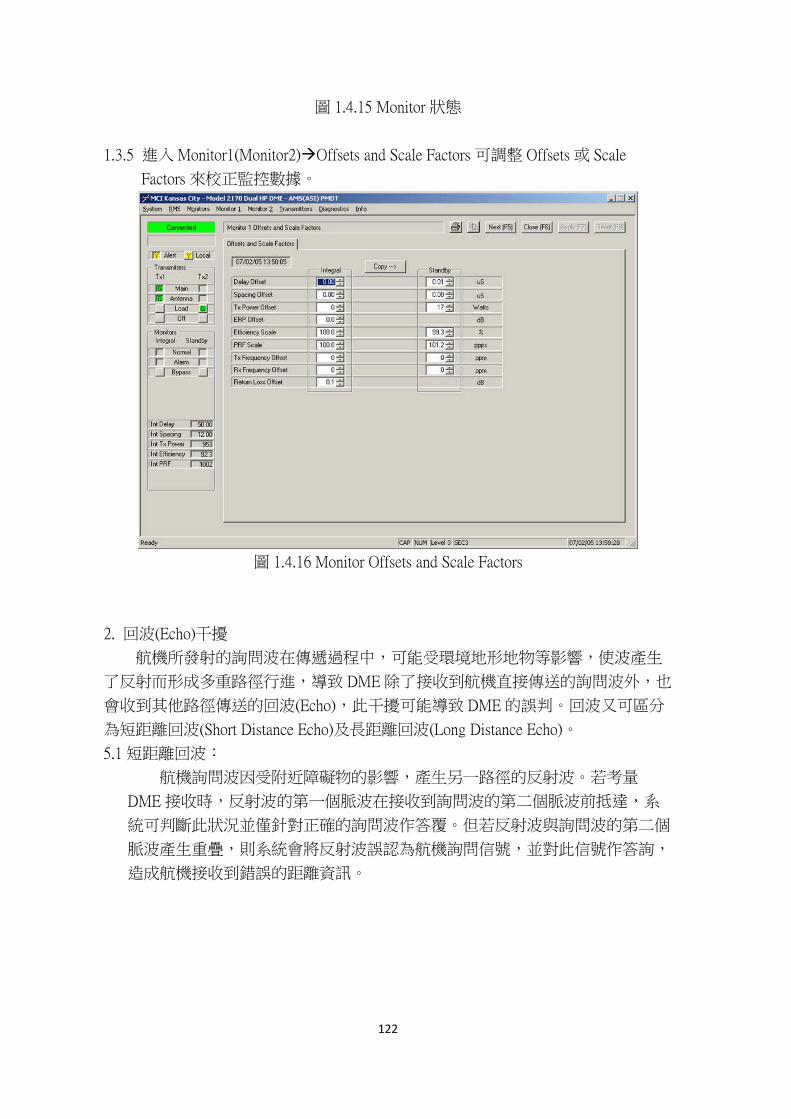
122
圖 1.4.15 Monitor 狀態
1.3.5 進入 Monitor1(Monitor2)�Offsets and Scale Factors 可調整 Offsets 或 Scale
Factors 來校正監控數據。
圖 1.4.16 Monitor Offsets and Scale Factors
2. 回波(Echo)干擾
航機所發射的詢問波在傳遞過程中,可能受環境地形地物等影響,使波產生
了反射而形成多重路徑行進,導致 DME 除了接收到航機直接傳送的詢問波外,也
會收到其他路徑傳送的回波(Echo),此干擾可能導致 DME 的誤判。回波又可區分
為短距離回波(Short Distance Echo)及長距離回波(Long Distance Echo)。
5.1 短距離回波:
航機詢問波因受附近障礙物的影響,產生另一路徑的反射波。若考量
DME 接收時,反射波的第一個脈波在接收到詢問波的第二個脈波前抵達,系
統可判斷此狀況並僅針對正確的詢問波作答覆。但若反射波與詢問波的第二個
脈波產生重疊,則系統會將反射波誤認為航機詢問信號,並對此信號作答詢,
造成航機接收到錯誤的距離資訊。
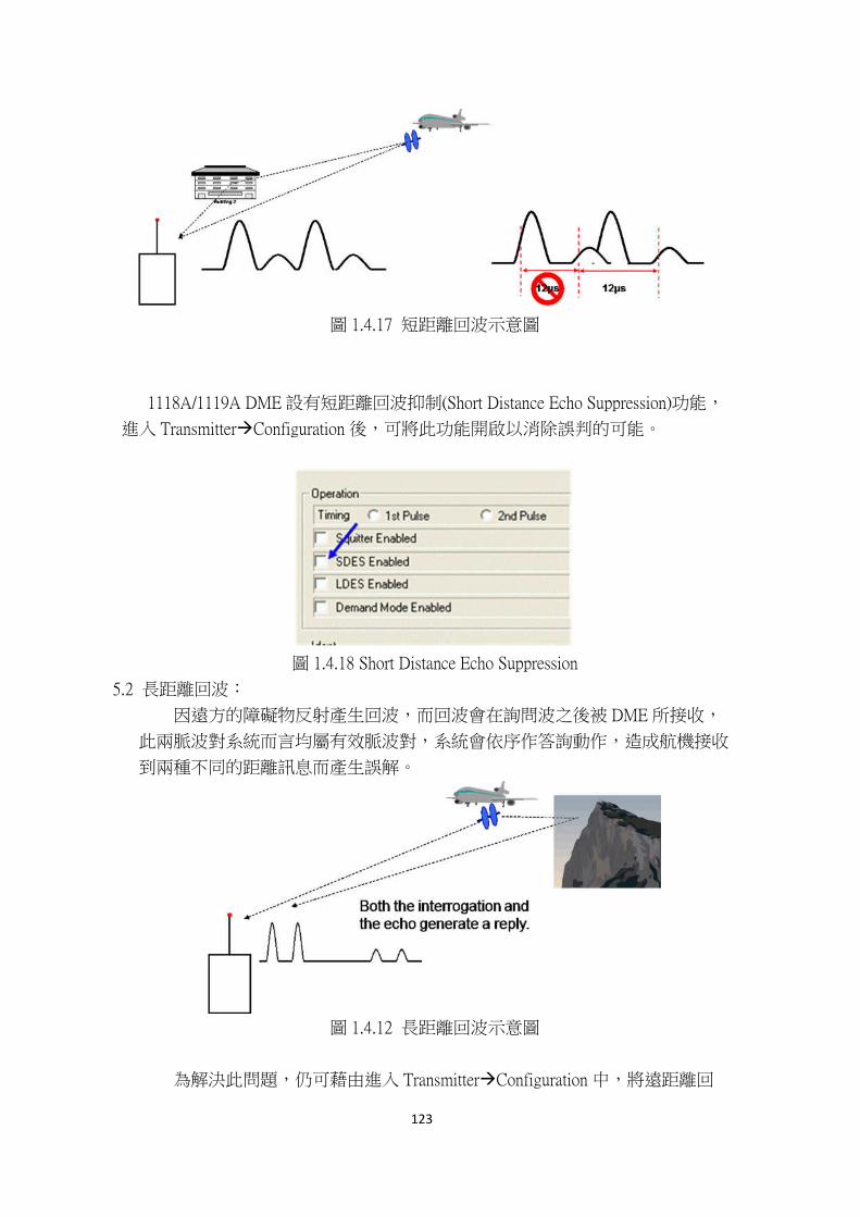
123
圖 1.4.17 短距離回波示意圖
1118A/1119A DME 設有短距離回波抑制(Short Distance Echo Suppression)功能,
進入 Transmitter�Configuration 後,可將此功能開啟以消除誤判的可能。
圖 1.4.18 Short Distance Echo Suppression
5.2 長距離回波:
因遠方的障礙物反射產生回波,而回波會在詢問波之後被 DME 所接收,
此兩脈波對系統而言均屬有效脈波對,系統會依序作答詢動作,造成航機接收
到兩種不同的距離訊息而產生誤解。
圖 1.4.12 長距離回波示意圖
為解決此問題,仍可藉由進入 Transmitter�Configuration 中,將遠距離回
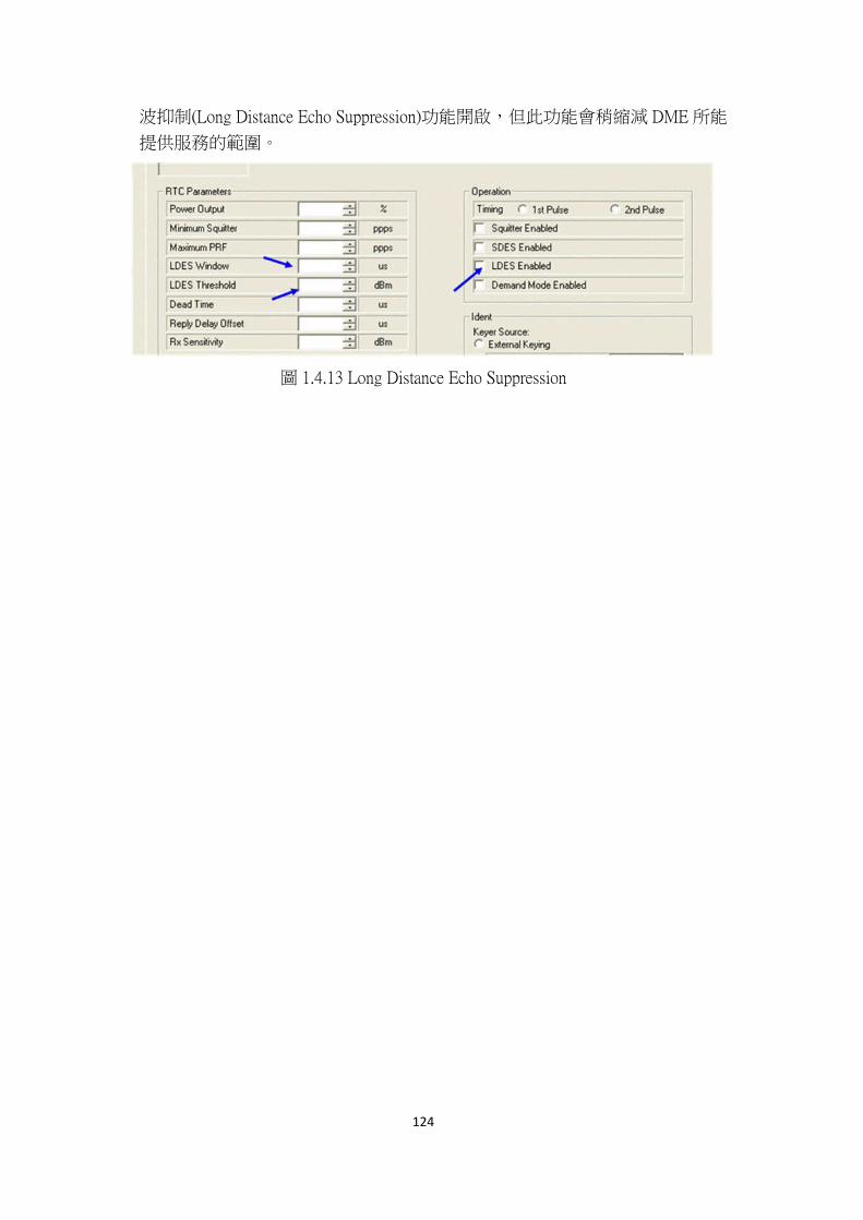
124
波抑制(Long Distance Echo Suppression)功能開啟,但此功能會稍縮減 DME 所能
提供服務的範圍。
圖 1.4.13 Long Distance Echo Suppression
125
肆肆肆肆、、、、 心心心心得與建議得與建議得與建議得與建議
本次藉著新增松山機場 VOR/DME 設備的機會,獲派至美國堪蕯斯參加工廠
訓練,備感榮幸的同時,也深覺責任重大;學員除了利用本次難能可貴的機會努
力提升自我能力,更要將寶貴資訊帶回臺灣,為提升我國航電人員能力及飛航服
務品質共同努力。
本次獲派參加受訓的成員共計 2 員,在異地生活上不但可以相互照應,也可
在課程中、課後時間共同研討、切磋學習,對於學習成效上助益良多。此外,也
承蒙授課教官 George Stone 及行政人員 Ruth Charpie 小姐於生活及交通上的照料及
協助,使得受訓期間十分愉快。
教官 George Stone 教學非常認真,授課內容深入淺出,從設備原理、模組功
能、參數設定及規範等詳細介紹,並十分注重學員的反應與吸收程度,學員困惑
處,必定詳加解說解惑。在受訓過程中收獲最多的,莫過於能接受原廠教官的第
一手知識與經驗;例如在 DME 授課前,訓練用之 DME 設備處於告警無法正常工
作的狀態,在教官的帶領下,依序檢測設備中的各模組工作正常與否,確認系統
參數設定是否正確等步驟,進而將故障排除,使系統得以恢復正常發射,這是極
為珍貴的一課!對於一位航電維護人員而言,能有條不紊地排除故障是非常重要
且必備的能力!
其二為學員能親自反覆練習操作設備,並在教官安排的 Trouble Shooting 課程
中,學習獨自查修設備。經驗往往在不斷練習中逐漸累積,然而過去本總臺大部
份為線上使用設備,啟用後鮮少可讓維護同仁進行大幅的調整操作,僅能在遇突
發狀況時,隨著前輩維修吸取經驗,然囿於設備修復有其急迫性,無法使同仁做
長期的檢測,其成效有限。有鑑於此,本總臺業已於本(103)年度於清泉崗機場成
立航電人員訓練中心,並辦理新進人員訓練及航電同仁複訓,藉由中心訓練用之
設備,使同仁有更多機會練習與操作,必能對本總臺航電人員有極大的助益!並
期待能帶來與工廠訓練之相同效果!
然而在本次的受訓過程中,提出以下幾點建議供長官及同仁參考:
1. SELEX 訓練中心並無餐廳且周邊亦無餐館,每日午餐須由受訓學員自行張
羅,備感不便。日後若有同仁獲派出國受訓機會,建議事先與原廠溝通能否提
供代訂午餐服務,定能使得受訓期間的生活機能更加完美!
2. 由於出國受訓員額有限,加上政府財政日益困難,國外出差旅費更加緊縮,在
無法派遣更多航電人員出國參加訓練又期望提升全體同仁能力的情況下,建議
126
可增加國內訓練天數及實務課程時間,使站台所有維護人員均能具備幾乎等同
國外訓之維修能力,進而增加更多的種子教官及維修能力之傳承;在清泉崗航
電人員訓練中心硬體設備逐步完善的同時,期待「軟體」實力也能不斷提升、
進步!
3. 本次於 SELEX 受訓期間僅本總臺 2 員參與,而結訓後緊接著為他國航電人員
參加訓練,且科目有部份重疊。建議往後安排受訓時間,可先行與原廠洽詢,
在人數不致影響本國同仁操作設備等權益的情況下,可考慮採併班受訓。畢竟
於國內受訓,僅可達到本國同仁能力的自我提升,卻無法與國際間產生知己知
彼的效果;若能藉由出國受訓的機會,增進與他國航電人員多方交流,不但能
在各國的不同的經驗與思維中學習更多,更能汲取他人之長處來補己之短,相
信對於我國同仁以及本總臺的未來都有莫大的助益!