Embed Size (px)
Citation preview
doi.org/10.26434/chemrxiv.12366623.v4
Saturation Profile Based Conformality Analysis for Atomic LayerDeposition: Aluminum Oxide in Lateral High-Aspect-Ratio ChannelsJihong Yim, Oili Ylivaara, Markku Ylilammi, Virpi Korpelainen, Eero Haimi, Emma Verkama, Mikko Utriainen,Riikka Puurunen
Submitted date: 23/09/2020 • Posted date: 23/09/2020Licence: CC BY-NC-ND 4.0Citation information: Yim, Jihong; Ylivaara, Oili; Ylilammi, Markku; Korpelainen, Virpi; Haimi, Eero; Verkama,Emma; et al. (2020): Saturation Profile Based Conformality Analysis for Atomic Layer Deposition: AluminumOxide in Lateral High-Aspect-Ratio Channels. ChemRxiv. Preprint.https://doi.org/10.26434/chemrxiv.12366623.v4
ABSTRACT: Atomic layer deposition (ALD) raises global interest through its unparalleled conformality. Thiswork describes new microscopic lateral high-aspect-ratio (LHAR) test structures for conformality analysis ofALD. The LHAR structures are made of silicon and consist of rectangular channels supported by pillars.Extreme aspect ratios even beyond 10 000:1 enable investigations where the adsorption front does notpenetrate to the end of the channel, thus exposing the saturation profile for detailed analysis. We use thearchetypical trimethylaluminum (TMA)-water ALD process to grow alumina as a test vehicle to demonstratethe applicability, repeatability and reproducibility of the saturation profile measurement and to provide abenchmark for future saturation profile studies. Through varying the TMA reaction and purge times, weobtained new information on the surface chemistry characteristics and the chemisorption kinetics of thiswidely studied ALD process. We propose new saturation profile related classifications and terminology.
File list (1)
download fileview on ChemRxivJ.Y.and O.Y. et al._Chemrxiv_20200922.pdf (5.53 MiB)
1
Saturation profile based conformality analysis for atomic layer deposition: alumi-1
num oxide in lateral high-aspect-ratio channels 2
Jihong Yim, a,x Oili M. E. Ylivaara,b,x Markku Ylilammi,c Virpi Korpelainen,b Eero Haimi,a Emma Verkama,a Mikko Utriainen,b 3
and Riikka L. Puurunen*,a,b 4
KEYWORDS: Lateral high-aspect-ratio (LHAR), Atomic layer deposition (ALD), Conformality, Saturation profile, 5
Aluminum oxide, trimethylaluminum, Kinetics, Sticking coefficient.d 6
ABSTRACT: Atomic layer deposition (ALD) raises global interest through its unparalleled conformality. This work 7
describes new microscopic lateral high-aspect-ratio (LHAR) test structures for conformality analysis of ALD. The 8
LHAR structures are made of silicon and consist of rectangular channels supported by pillars. Extreme aspect ratios 9
even beyond 10 000:1 enable investigations where the adsorption front does not penetrate to the end of the 10
channel, thus exposing the saturation profile for detailed analysis. We use the archetypical trimethylaluminum 11
(TMA)-water ALD process to grow alumina as a test vehicle to demonstrate the applicability, repeatability and 12
reproducibility of the saturation profile measurement and to provide a benchmark for future saturation profile 13
studies. Through varying the TMA reaction and purge times, we obtained new information on the surface chem-14
istry characteristics and the chemisorption kinetics of this widely studied ALD process. New saturation profile 15
related classifications and terminology are proposed. 16
a Department of Chemical and Metallurgical Engineering, Aalto University School of Chemical Engineering, Kemistintie 1, Espoo, Finland
b VTT Technical Research Centre of Finland, PL 1000, 02044 VTT, Finland
c Espoo, Finland
d Electronic Supplementary information (ESI) available: extended information on Experimental, Results, and Discussion sections.
2
A. Introduction 17
Conformality refers to the ability to coat a three-dimensional object with a homogeneous coating of uniform 18
thickness.1,2 Conformal coatings are required in the fabrication of state-of-the-art and future electronics,2–4 as well 19
as in various applications related to heterogeneous catalysts,5–8 biosensors,9 and energy industries.10,11 Atomic 20
layer deposition (ALD),12–15 a variant of chemical vapor deposition (CVD), was invented independently over forty 21
years ago under the names atomic layer epitaxy16–19 and molecular layering.20–22 The Millennium Technology Prize 22
was awarded to ALD’s Finnish inventor, Tuomo Suntola in 2018.23 ALD is gaining increasing interest as the method 23
of choice for conformal thin film growth.1,2 The unique features of ALD are the systematic use of self-terminating 24
gas-solid reactions and precise film thickness control at subnanometer level.13,14,24 When the gas-solid reactions 25
are completed, they stop by themselves. This adsorption control results in the unparalleled conformality of ALD 26
films.1,25–27 27
Despite the inherent advantage of ALD, the conformal coating of a certain aspect ratio (AR) is not guaran-28
teed.1,8,28 Thus, the tuning of ALD process parameters is needed to achieve a homogeneous coating in high-aspect-29
ratio (HAR) structures.1,29–31 For an ideal ALD process, the penetration depth of a coating is known to scale with 30
the square root of the reactant dose, where the dose equals partial pressure of reactant multiplied by exposure 31
time.29,32–34 The reactivity of the compounds, often described by a (lumped) sticking coefficient cA (A stands for 32
Reactant A), further influences the speed at which uniform thickness is attained.1,31,35,36 Non-ideal reactions, such 33
as unwanted CVD through decomposition of one of the reactants or through the mixing of reactant pulses, or non-34
saturation of the reactions, would compromise the conformality.1,37 35
A practical industry standard of conformality measurements has been vertical HAR (VHAR) structures etched 36
into silicon. Scanning or transmission electron microscopy (SEM or TEM) images acquired after careful specimen 37
preparation allow the film thickness and step coverage (ratio of the film thickness at the bottom of a feature to 38
film thickness at the top of the feature) to be determined.1,2,29,34,35,38 Sometimes, the (lumped) sticking coefficient 39
has been extracted from the (often sparse) data.35 40
3
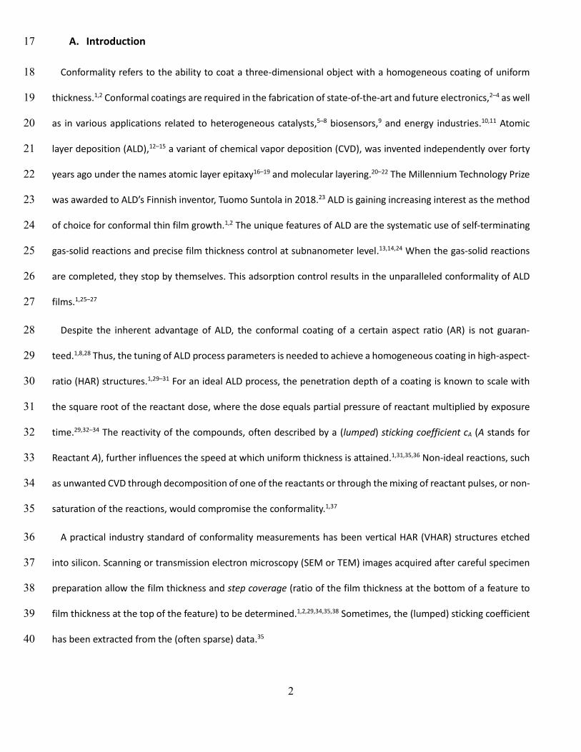
As an alternative to VHAR, lateral HAR (LHAR) structures have emerged. Figure 1 illustrates the concept of con-41
formality analysis with LHAR channels. By removing the roof of the channel after ALD, the film is exposed for top-42
view analysis by methods suitable for planar surfaces. Most often, LHAR structures are intentionally fabricated 43
with such demanding aspect ratios that the film does not reach the end of the features, which enables analysis of 44
what we call the saturation profile of the ALD process. 45
Various types of LHAR structures appear in the literature. For example, Dendooven et al.31,39 assembled macro-46
scopic LHAR structures with a rectangular channel, and the channel height in the hundreds of micrometers. Gao 47
et al.40 microfabricated LHAR cavities expanding from elongated circles with single-crystal silicon at the bottom, 48
polysilicon as the roof, and silicon dioxide pillars supporting the structure; the design cavity height was 200, 500, 49
or 1000 nm and the ARs above 10000:1. We will refer to the structures by Gao et al.40 as PillarHall-1 (from Pil-50
larHall™, 1st generation). In turn, Schwille et al.30,41 fabricated centrosymmetric LHAR cavities resembling struc-51
tures used in microelectromechanical systems (MEMS) processing; here, the limiting gap height was 4.5 µm. Re-52
cently, building upon the process of Gao et al.,40 improved microscopic rectangular LHAR channels have been 53
developed and used, but not yet described in detail;33,36,42–44 describing them is among the goals of this work. 54
LHAR structures have been employed to study the conformality of an emerging small minority of the more than 55
700 published ALD processes;45 Al2O3 from Me3Al (TMA) and H2O;30,31,33,36,40,46 TiO2 from TiCl4 and H2O;40 Ir and IrOx 56
from Ir(acac)3 and various reactants;47 HfSiOx from Hf[N(CH3)(C2H5)]4, SiH[N(CH3)2]3, and O3;42 SiO2 from 57
SiH2[N(CH2CH3)2]2 and O3;41 plasma enhanced ALD (PEALD) of Al2O3 and AlN from TMA, and O2 and NH3 plasma;39 58
and PEALD of SiO2, TiO2, Al2O3 and HfO2 from SiH2(N(C2H5)2)2, Ti(N(CH3)2)4, TMA and HfCp(N(CH3)2)3 and O2/Ar 59
plasma.44,48 60
61
4
Figure 1. Schematic illustration of the conformality analysis with LHAR channels: (a) uncoated channel, (b) channel after ALD 62
coating and (c) channel after removing the roof and exposing the surface for analysis. H is the height and L the length of the 63
LHAR channel. The illustration is intentionally not in scale: typical aspect ratios L : H in LHAR structures are at least 200 : 1 and 64
the ratios in this work are typically up to 10000 : 1. 65
Common to LHAR approaches has typically been to measure the saturation profile of the ALD process and to 66
extract kinetic information of the film growth through modelling.1 Often, a model is assuming either reversible or 67
irreversible single-site Langmuir adsorption (A + * ⇌ A*) to describe an ALD reaction step, and the (lumped) stick-68
ing coefficient for the reaction is extracted from fitting a model to the saturation profile.30,31,33,36 For example, 69
Dendooven et al.31 extracted the sticking coefficient of TMA on Al2O3 and studied its effect on step coverage with 70
LHAR features. They also combined LHAR studies with a Monte Carlo algorithm to study the conformality of Al2O3 71
and AlN by PEALD.39 Schwille et al30,41 determined the sticking coefficient of TMA and bis-diethyl aminosilane 72
(BDEAS) by using a Monte Carlo process simulation and data obtained with LHAR features. Ylilammi et al.33 ex-73
tracted the lumped sticking coefficient of TMA on Al2O3 and TiCl4 on TiO2 using a diffusion–reaction model of ALD 74
saturation profile over LHAR features. Arts et al.36 extracted, by using LHAR features, the lumped sticking coeffi-75
cient directly from the slope of the saturation profile and the recombination probability of O2 plasma radicals 76
during PEALD of various oxides from the PEALD film’s penetration depth.44 77
This work aims to create a benchmark for saturation profile based conformality analysis of ALD processes with 78
microscopic LHAR structures. We chose the archetypical TMA-water process13,15,49 —at the ALD temperature most 79
typically employed for it, 300°C— as a test vehicle for the saturation profile analysis development, because this 80
process is known as a near-ideal ALD process,13–15 because this process has already been studied with LHAR struc-81
tures,30,31,33,36,40,46 and because the details of the surface chemistry and kinetics of this process continue to be the 82
subject of scientific investigations and debate.13,50–57 The repeatability and reproducibility of the saturation profile 83
measurement are assessed. New information is obtained on the surface chemistry and chemisorption kinetics of 84
the TMA-water process as a function of TMA dose and purge times. New saturation profile related classifications 85
and terminology are developed, with applicability beyond this work. We hope that once the practicalities and 86
5
limitations of the saturation profile analysis are well described for this TMA-water process, conformality studies 87
of other ALD processes—and even of other thin film processes such as CVD and atomic layer etching (ALE)—can 88
be compared and contrasted against this benchmark. 89
B. Saturation profile terminology 90
This section develops and discusses terminology related to saturation profiles before entering into experimental 91
details. 92
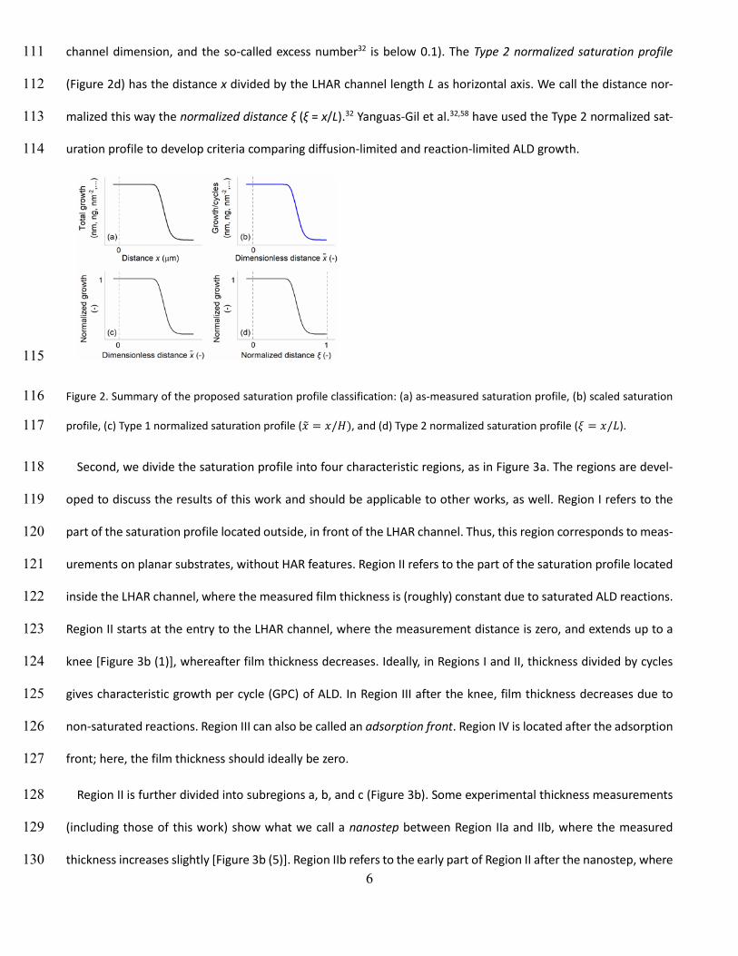
First, we propose a general classification of saturation profile types in LHAR features, as in Figure 2. Examples 93
are provided where these four classes have been used in the literature; combinations of classes have also been 94
used. The as-measured saturation profile is obtained directly from the measurement with a measure of the total 95
growth as the vertical axis and distance as the horizontal axis (Figure 2a). Dendooven et al.39 and Ylilammi et al.,33 96
for example, used an as-measured saturation profile to present the effect of process parameters on the confor-97
mality of PEALD and ALD. 98
The scaled saturation profile has the total growth divided by cycles as the vertical axis and the measurement 99
distance x divided by the channel height H as the horizontal axis (Figure 2b). We call the distance scaled this way 100
the dimensionless distance �̃� (�̃� = 𝑥/𝐻). Earlier, AR has often been used as the horizontal axis in a way analogous 101
to the dimensionless distance used in this article.1,2,40,47 Advantageously, this dimensionless distance is a well-102
defined physical quantity that remains constant irrespective of the extent of growth, while the AR experienced by 103
the ALD process increases during the process with increasing film thickness through narrowing of the channel. 104
The scaled saturation profile can be further normalized in (at least) two distinct ways. The Type 1 normalized 105
saturation profile (Figure 2c) has the amount of growth at channel entrance normalized to one (optionally, this 106
value is interpreted as surface coverage θ,32,36 having values 0 θ 1) as the vertical axis and the dimensionless 107
distance �̃� as the horizontal axis. Arts et al.36 developed a method to determine a lumped sticking coefficient di-108
rectly from the slope of the Type 1 normalized saturation profile, provided that certain conditions prevail during 109
the ALD process (most importantly, that the molecule’s mean free path λ is significantly larger than the limiting 110
6
channel dimension, and the so-called excess number32 is below 0.1). The Type 2 normalized saturation profile 111
(Figure 2d) has the distance x divided by the LHAR channel length L as horizontal axis. We call the distance nor-112
malized this way the normalized distance ξ (ξ = x/L).32 Yanguas-Gil et al.32,58 have used the Type 2 normalized sat-113
uration profile to develop criteria comparing diffusion-limited and reaction-limited ALD growth. 114
115
Figure 2. Summary of the proposed saturation profile classification: (a) as-measured saturation profile, (b) scaled saturation 116
profile, (c) Type 1 normalized saturation profile (�̃� = 𝑥/𝐻), and (d) Type 2 normalized saturation profile (𝜉 = 𝑥/𝐿). 117
Second, we divide the saturation profile into four characteristic regions, as in Figure 3a. The regions are devel-118
oped to discuss the results of this work and should be applicable to other works, as well. Region I refers to the 119
part of the saturation profile located outside, in front of the LHAR channel. Thus, this region corresponds to meas-120
urements on planar substrates, without HAR features. Region II refers to the part of the saturation profile located 121
inside the LHAR channel, where the measured film thickness is (roughly) constant due to saturated ALD reactions. 122
Region II starts at the entry to the LHAR channel, where the measurement distance is zero, and extends up to a 123
knee [Figure 3b (1)], whereafter film thickness decreases. Ideally, in Regions I and II, thickness divided by cycles 124
gives characteristic growth per cycle (GPC) of ALD. In Region III after the knee, film thickness decreases due to 125
non-saturated reactions. Region III can also be called an adsorption front. Region IV is located after the adsorption 126
front; here, the film thickness should ideally be zero. 127
Region II is further divided into subregions a, b, and c (Figure 3b). Some experimental thickness measurements 128
(including those of this work) show what we call a nanostep between Region IIa and IIb, where the measured 129
thickness increases slightly [Figure 3b (5)]. Region IIb refers to the early part of Region II after the nanostep, where 130
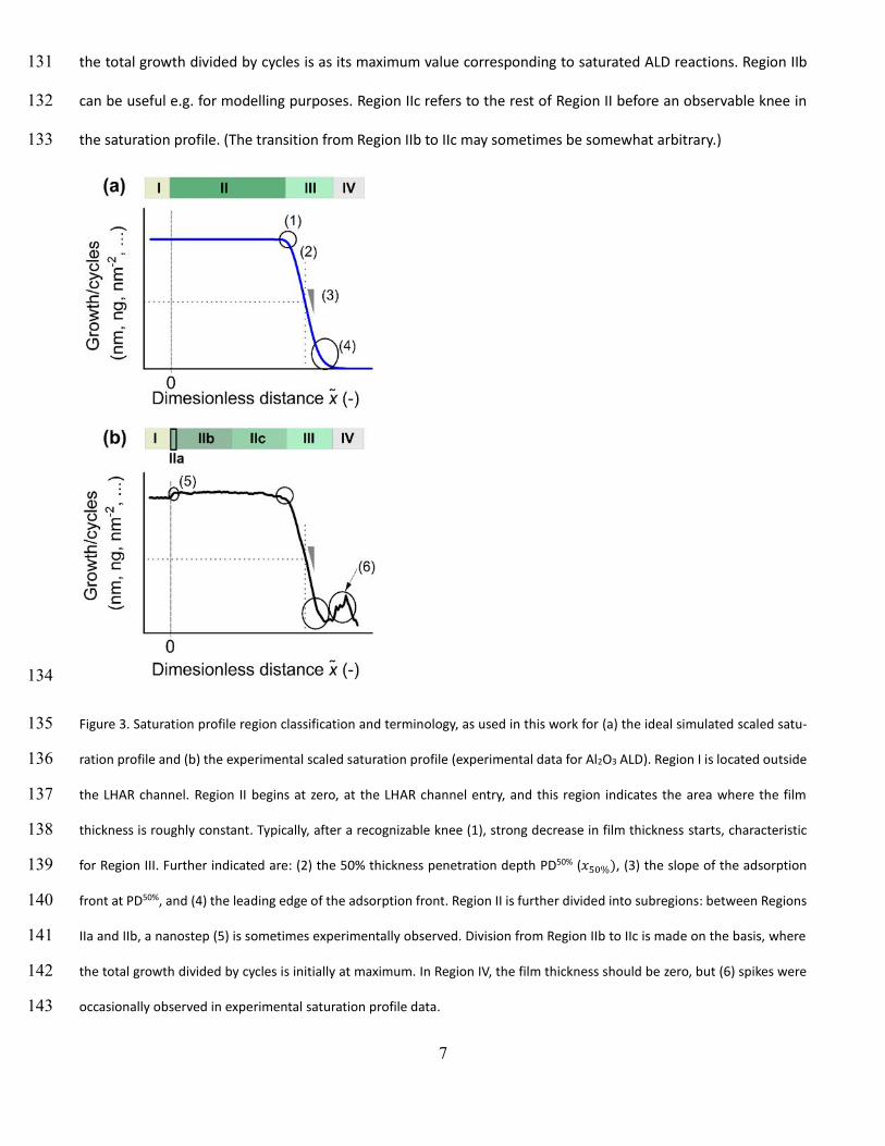
7
the total growth divided by cycles is as its maximum value corresponding to saturated ALD reactions. Region IIb 131
can be useful e.g. for modelling purposes. Region IIc refers to the rest of Region II before an observable knee in 132
the saturation profile. (The transition from Region IIb to IIc may sometimes be somewhat arbitrary.) 133
134
Figure 3. Saturation profile region classification and terminology, as used in this work for (a) the ideal simulated scaled satu-135
ration profile and (b) the experimental scaled saturation profile (experimental data for Al2O3 ALD). Region I is located outside 136
the LHAR channel. Region II begins at zero, at the LHAR channel entry, and this region indicates the area where the film 137
thickness is roughly constant. Typically, after a recognizable knee (1), strong decrease in film thickness starts, characteristic 138
for Region III. Further indicated are: (2) the 50% thickness penetration depth PD50% (𝑥50%), (3) the slope of the adsorption 139
front at PD50%, and (4) the leading edge of the adsorption front. Region II is further divided into subregions: between Regions 140
IIa and IIb, a nanostep (5) is sometimes experimentally observed. Division from Region IIb to IIc is made on the basis, where 141
the total growth divided by cycles is initially at maximum. In Region IV, the film thickness should be zero, but (6) spikes were 142
occasionally observed in experimental saturation profile data. 143
8
C. Experimental 144
A. Fabrication of conformality test chips 145
The conformality test chip prototypes reported in this work with all-silicon LHAR channels (Figure S1) were pro-146
duced with MEMS processing techniques using a process modified from Gao et al.40 (PillarHall-1). The test chip 147
prototypes of this work are identified as PillarHall™ 3rd generation, or PillarHall-3, in short. Starting substrates 148
were low-doped 150 mm silicon (100) wafers. The process encompassed typically thermal silicon oxide layer 149
growth to the targeted channel height H (100, 500, or 2000 nm); polysilicon membrane deposition from silane 150
(SiH4) in multiple steps; several photolithography steps; a plug-up process;40 and HF vapor etching as the final 151
fabrication step. Wafers were optionally diced to the 15 x 20 mm chip size. The processing for a distance indicator 152
scale on top of the membrane for optical analysis was an optional step (Figure S2). Thermal oxidation and polysil-153
icon deposition were made with Centrotherm E1200 HT 260-4 furnaces, and HF etching with Primaxx MEMS-CET 154
HF vapor etcher. Contact lithography was made with a SUSS Mask aligner MA150 and stepper lithography with a 155
Canon FPA3000-i4 (i-line) Wafer stepper. 156
The conformality test chip prototypes have various LHAR channels with ARs up to 10,000:1, when the lateral 157
length L is 5000 µm, and the targeted channel height is 500 nm (Table S1). The conformality chip layout details 158
and pillar layout designs are included in the supporting information. 159
B. Atomic layer deposition 160
ALD Al2O3 films were grown at 300 °C in a Picosun R-150 ALD reactor. The target thickness was typically ca. 50 161
nm made in 500 ALD cycles. The process pressure was ca. 3 hPa. Nitrogen (purity 6.0) with a constant flow rate of 162
150 sccm was used as the carrier and purge gas through four reactant lines. Similar to earlier studies,33,40,51 a TMA-163
purge-water-purge sequence (s) of 0.1-4.0-0.1-4.0 was typically used. The pyrophoric TMA was handled inertly. 164
The samples and the experimental variables used are listed in Table 1. 165
To study the effect of the pillar density on the saturation profile, Al2O3 films were coated in LHAR channels with 166
different pillar designs of layout v1a, v1b, and v2a (design channel height: 500 nm), which had been fabricated on 167
9
the same silicon wafer. Table S2 and Figure S3 report the detailed information on different pillar designs. All of the 168
films were grown in the same ALD run to avoid run-to-run variations (Series A in Table 1). 169
C. Characterization methods 170
In this work, the ALD Al2O3 film was characterized after peeling off the top membrane with adhesive tape, as 171
shown in Figure 1c, unless stated otherwise. Optical microscopy was routinely used to image the coated LHAR 172
channels, before and after peeling off the top membrane with adhesive tape. 173
Scanning electron microscopy (SEM) with energy-dispersive X-ray spectrometry (EDS) was performed using a 174
Tescan Mira3 SEM fitted with a Thermo Scientific EDS. An accelerating voltage of 5 keV was used for the SEM-EDS 175
line scan. The sample with the design channel height of 500 nm had been stored in ambient air. Thus, no sample 176
preparation for charging prevention was required. Elemental x-ray mapping of the sample surface was performed 177
first. Subsequently, line scans of elemental profiles were measured. The length of the line was 500 µm with meas-178
urement points at 1 µm intervals. Outliers due to pillars and edges in surface channels were removed from the 179
elemental profile results. The line scans are averages of five measurements. 180
The surface topography was measured by using a PSIA XE-100 atomic force microscope (AFM). Non-contact 181
mode and standard types of AFM tips were used in the measurements. The measurement area varied from 10 µm 182
× 10 µm to 90 µm × 90 µm, and resolution was 1024 × 256 pixels. Sample tilt and drift in slow scan direction were 183
corrected using line wise first order polynomial fit. 184
The saturation profiles of ALD Al2O3 films were measured by a spectroscopic reflectometer line scan (FilmTek 185
2000M wavelength range of 380 to 800 nm). The line scans began outside the channel in Region I of Figure 3 (ca. 186
13 µm before channel entry). The total scan length was 198 or 398 µm with a step of 2 µm, and 100 to 200 data 187
points were obtained. If not otherwise stated, a 50X objective lens with an estimated spot size of 5-6 µm was used. 188
To study the effect of spot size on the saturation profile, 10X and 5X objective lenses with an estimated spot size 189
of 25 and 50 µm, respectively, were used. To analyze the repeatability of the measurement at one location and 190
within-chip reproducibility, the reflectometry measurements were repeated several times on each of the lateral 191
lengths (pillar layout v1b). The thickness of the films coated on LHAR channels having different lateral lengths L 192
10
(0.1 to 5 mm) was measured several times. Then we excluded outliers and averaged the thickness except for the 193
Series B in Table 1 for which L of 5 mm data was used. This method gave us more representative results than 194
treating single thickness scans. 195
D. Saturation profile simulation 196
A series of simulations was performed using a MATLAB implementation of the diffusion–reaction model devel-197
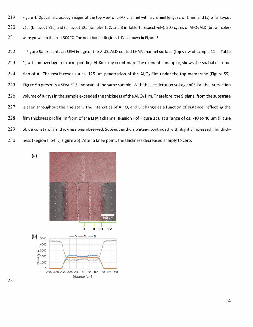
oped by Ylilammi et al. 2018.33 In the simulated conditions, the mean free path1 of TMA λTMA is ca. 40 µm. The 198
partial pressure of Reactant A was calculated with the discretized approximate solution to the one-dimensional 199
diffusion equation, presented in Equations (17-28) in Ref.33. An additional simplification was made in the calcula-200
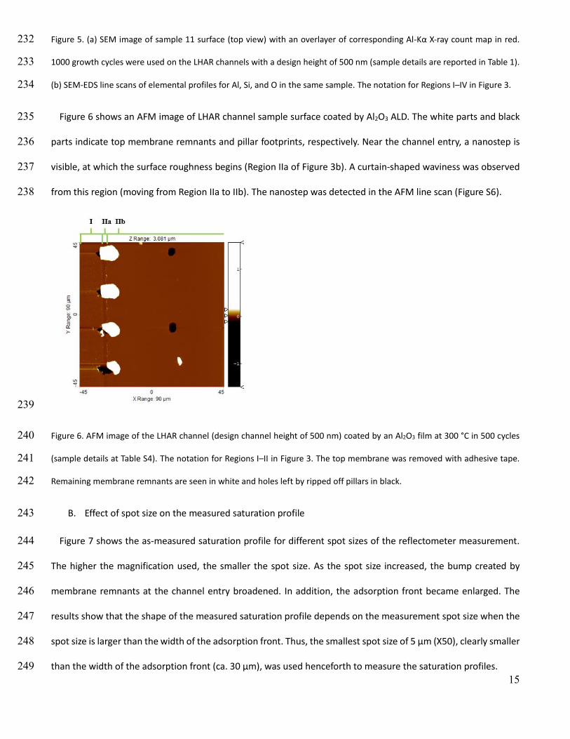
tion of the gas phase diffusion constant of Reactant A (Equation 3 in Ref.33), where the collision rate of molecules 201
at location x and time t was replaced with the collision rate of molecules at location x at the previous time step, t-202
1. The discretized partial differential equation describing the surface coverage as a function of time and location, 203
Equation (31) in Ref.33 was solved with the MATLAB® ODE23 ordinary differential equation solver, where the rel-204
ative tolerance was set to 10-3 and the absolute tolerance was specified at 10-5. During the implementation, a 205
mistake was found in the original article, both terms on the right side of Equation (1) in Ref.33 should be multiplied 206
by Avogadro’s number. 207
11
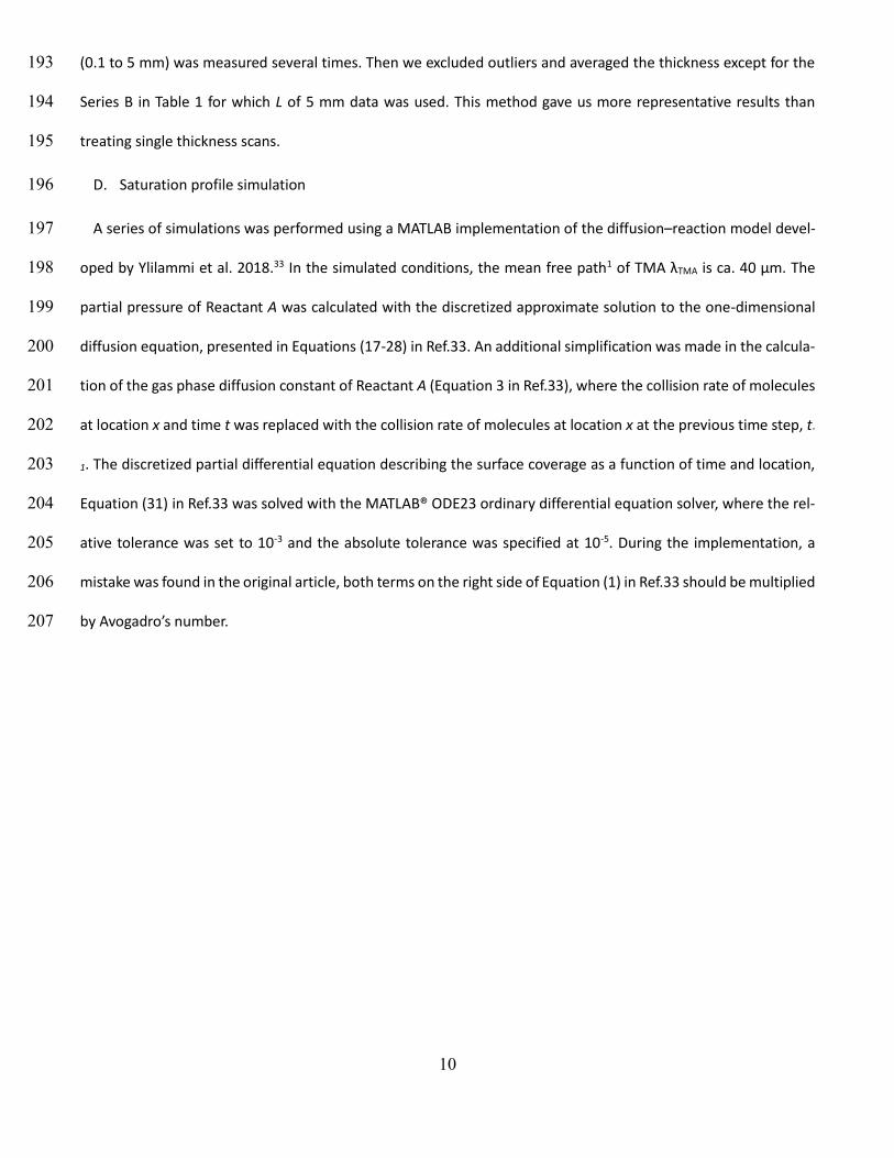
Table 1. Summary of experimental parameters used and saturation profile features measured by reflectometer for ALD Al2O3 film grown in the
LHAR channel at 300 °C (varied parameters bolded)
Se-ries
a)
Sam-ple
code b)
Pulse-purge sequence (s)
Design chan-
nel height H (nm)
f)
Pillar layout
ALD cy-cles N
Reflec-tome-
ter Magni-fication
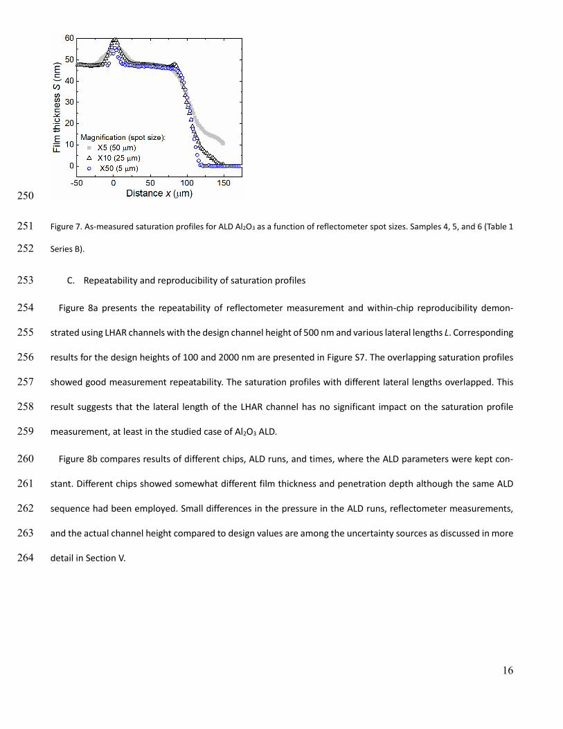
Thick-ness
outside SI
(nm)
Initial thickness
SIIb c) (nm)
SI/N (GPCI) (nm)
SIIb/N (GPCIIb)
(nm)
𝑥50%
(PD50%)
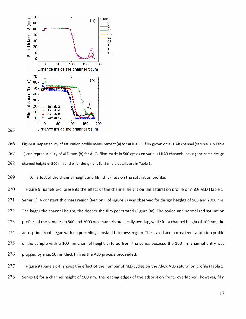
(µm)
�̃�50% (-)
slope d) 𝑑(𝑆/𝑁)
𝑑�̃�
(nm)
slope 𝑑𝜃
𝑑�̃�
(-)
Linear fitting resid-ual R2
1 0.1-4.0-0.1-4.0 500 v1a 500 X50 49.8 53.3 0.100 0.107 140 280 -0.0013 -0.013 0.983
A 2 0.1-4.0-0.1-4.0 500 v1b 500 X50 49.6 54.5 0.0993 0.109 140 280 -0.0013 -0.011 0.991
3 0.1-4.0-0.1-4.0 500 v2a 500 X50 50.5 53.4 0.101 0.107 110 220 -0.0018 -0.018 0.997
4 0.1-4.0-0.1-4.0 500 v1b 500 X50 47.4 47.8 0.0949 0.0956 105 208 -0.0018 -0.019 0.993
B 5 0.1-4.0-0.1-4.0 500 v1b 500 X10 49.1 50.0 0.0983 0.100 103 208 -0.0015 -0.015 0.998
6 0.1-4.0-0.1-4.0 500 v1b 500 X5 51.4 52.9 0.103 0.106 109 214 -0.00087 -0.0083 0.998
7 0.1-4.0-0.1-4.0 100 v1b 500 X50 - e) 47.8 - 0.0955 10 100 -0.00048 -0.0050 0.995
C 8 0.1-4.0-0.1-4.0 500 v1b 500 X50 46.7 51.1 0.0934 0.102 106 214 -0.0020 -0.019 0.993
9 0.1-4.0-0.1-4.0 2000 v1b 500 X50 45.3 48.8 0.0906 0.0976 375 188 -0.0046 -0.047 0.995
10 0.1-4.0-0.1-4.0 500 v1b 250 X50 24.3 26.0 0.0970 0.104 115 230 -0.0022 -0.021 0.982
D 8 0.1-4.0-0.1-4.0 500 v1b 500 X50 46.7 51.1 0.0934 0.102 106 214 -0.0020 -0.019 0.993
11 0.1-4.0-0.1-4.0 500 v1b 1000 X50 94.7 99.3 0.0947 0.0993 95 190 -0.00099 -0.010 0.996
12 0.1-4.0-0.1-4.0 500 v1b 500 X50 47.5 50.2 0.0951 0.100 96 192 -0.0021 -0.021 0.971
E 13 0.2-4.0-0.1-4.0 500 v1b 500 X50 48.2 49.8 0.0962 0.100 133 266 -0.0014 -0.014 0.996
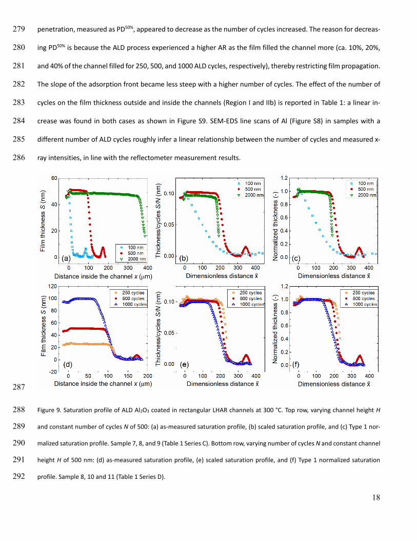
14 0.4-4.0-0.1-4.0 500 v2a 500 X50 48.6 51.0 0.0972 0.102 197 386 -0.00045 -0.0044 0.996
15
0.1-1.0-0.1-1.0
500 v1b 500 X50 50.4 51.9 0.101 0.104 99 198 -0.0017 -0.016 0.983
F 12
0.1-4.0-0.1-4.0
500 v1b 500 X50 47.5 50.2 0.0951 0.100 96 192 -0.0021 -0.021 0.971
16
0.1-10.0-0.1-10.0
500 v1b 500 X50 44.8 48.9 0.0897 0.0978 109 218 -0.0017 -0.018 0.999
12
a) Different pillar layout design for Series A; reflectometer magnification for Series B; design channel height for Series C; ALD cycles for Series D; TMA pulse
time for Series E; and purge time for Series F.
b) Original traceable sample codes in Supporting information, Table S3.
c) Initial film thickness SIIb was calculated as the average of the first five data points from the constant film thickness region (Region IIb, Figure 3). For the 100
nm channel height, the initial thickness is the first data point in a constant thickness region. The optically measured thickness includes the thickness of the
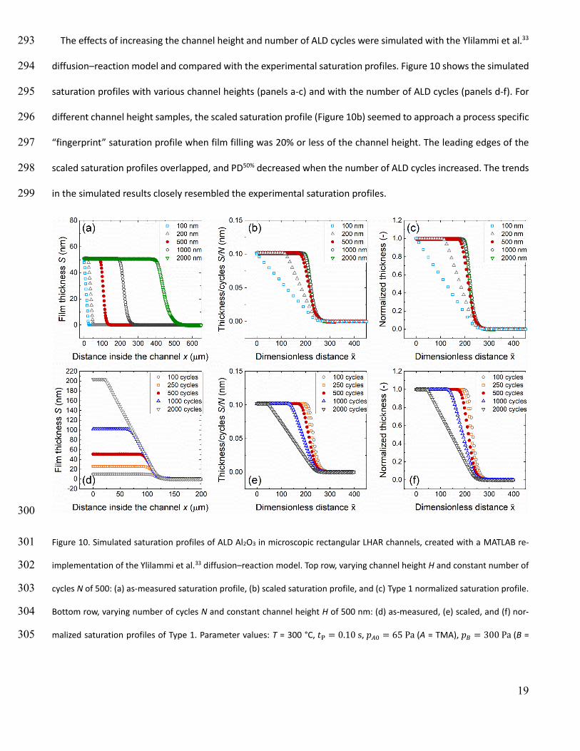
native silicon oxide.
d) The slope of the adsorption front (Region III of Figure 3) was extracted from the scaled saturation profile by finding the best-linear fitting line.
e) For the design channel height H of 100 nm, the film thickness outside the channel (Region I of Figure 3) was not measured.
f) For each design channel height H, the thickness of the film coated on channels having different lateral lengths L (0.1 to 5 mm) were measured several times
and averaged except for the Series B for which L of 5 mm data was used. Design aspect ratio of each channel is listed in Table S1.
13
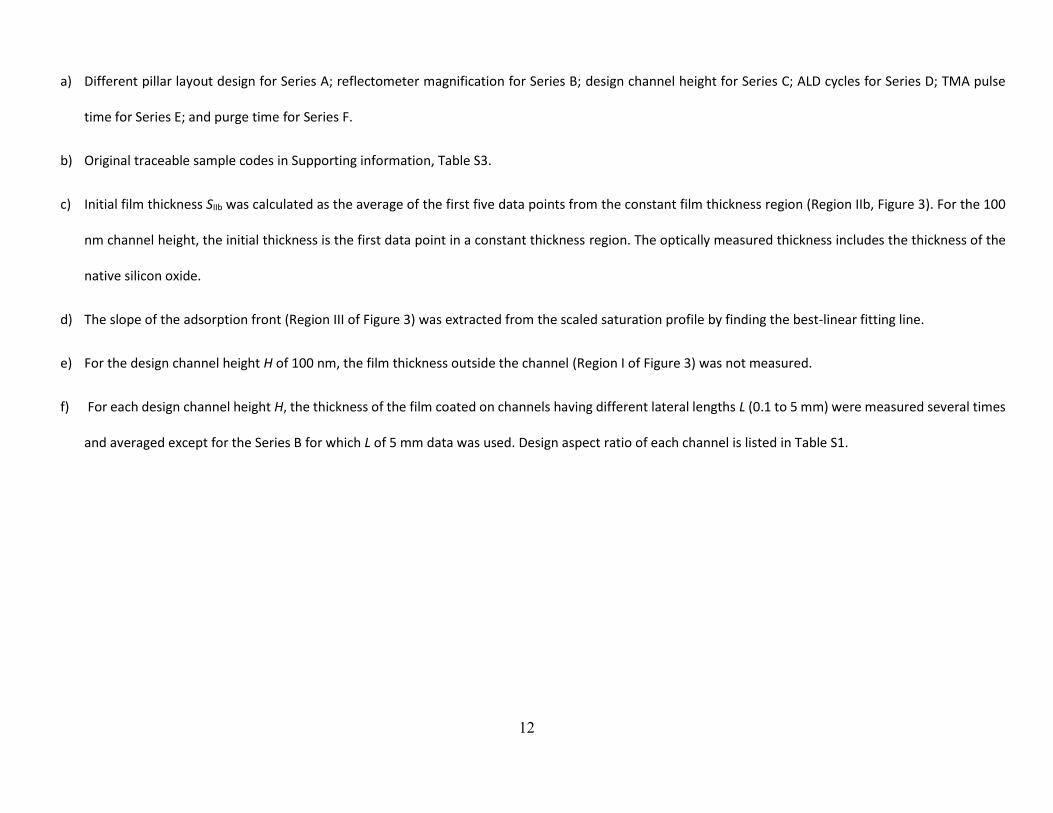
D. Results 207
A. Microscopic analysis of the coated area 208
Figure 4 presents optical microscopy images of ALD Al2O3 coated LHAR channels. The top membrane was re-209
moved before the analysis. The color difference reveals the coated area. For the pillar layouts v1a and v1b (Figure 210
4a and b), a penetration depth of ca. 140 µm from the channel entry was visually determined. A straight adsorption 211
front was observed parallel to the channel entry. Pillar layout v2a (Figure 4c) showed a wavy adsorption front and 212
a smaller penetration depth of ca. 100 µm. The smaller penetration depth most likely originated from the top 213
membrane hanging lower between the pillars; the hanging membrane likely resulted in a narrower channel than 214
the target. Figure S4 shows the saturation profiles for different pillar layout designs. For layouts v1a and v1b, 215
saturation profiles overlapped. Similar to the previous microscopy results, a lower penetration depth was also 216
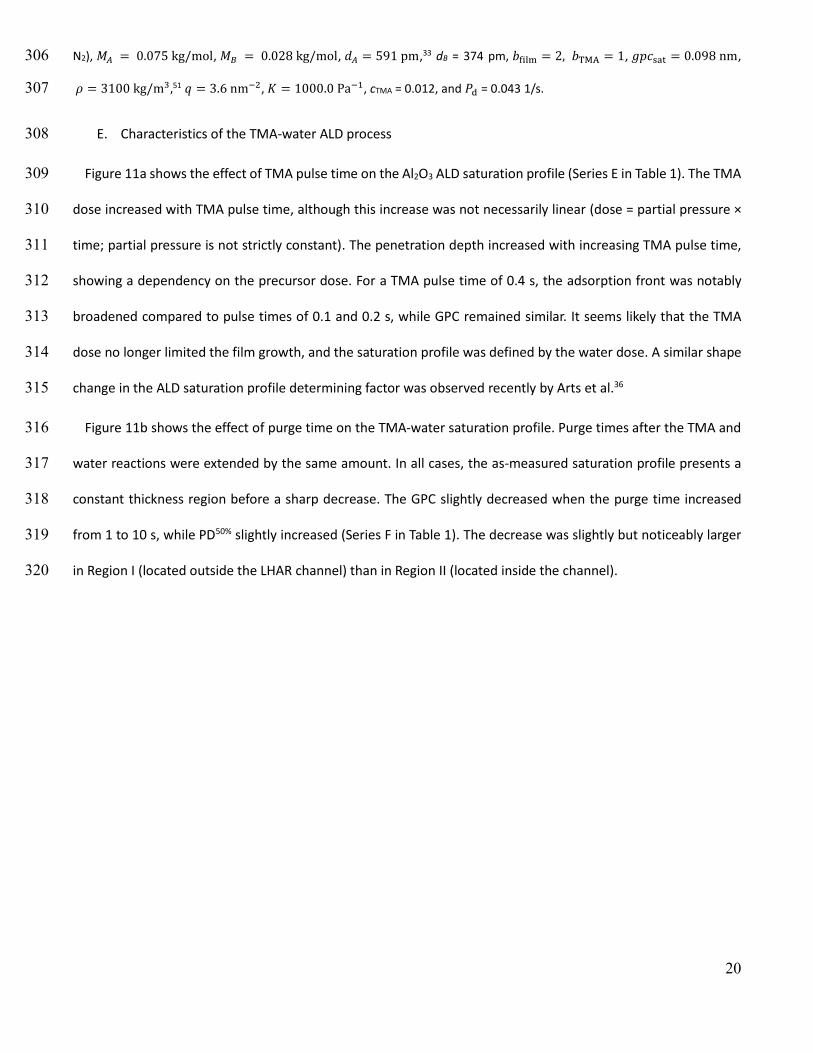
observed for layout v2a. 217
218
14
Figure 4. Optical microscopy images of the top view of LHAR channel with a channel length L of 1 mm and (a) pillar layout 219
v1a, (b) layout v1b, and (c) layout v2a (samples 1, 2, and 3 in Table 1, respectively). 500 cycles of Al2O3 ALD (brown color) 220
were grown on them at 300 °C. The notation for Regions I–IV is shown in Figure 3. 221
Figure 5a presents an SEM image of the Al2O3 ALD-coated LHAR channel surface (top view of sample 11 in Table 222
1) with an overlayer of corresponding Al-Kα x-ray count map. The elemental mapping shows the spatial distribu-223
tion of Al. The result reveals a ca. 125 μm penetration of the Al2O3 film under the top membrane (Figure S5). 224
Figure 5b presents a SEM-EDS line scan of the same sample. With the acceleration voltage of 5 kV, the interaction 225
volume of X-rays in the sample exceeded the thickness of the Al2O3 film. Therefore, the Si signal from the substrate 226
is seen throughout the line scan. The intensities of Al, O, and Si change as a function of distance, reflecting the 227
film thickness profile. In front of the LHAR channel (Region I of Figure 3b), at a range of ca. -40 to 40 µm (Figure 228
5b), a constant film thickness was observed. Subsequently, a plateau continued with slightly increased film thick-229
ness (Region II b-II c, Figure 3b). After a knee point, the thickness decreased sharply to zero. 230
231
15
Figure 5. (a) SEM image of sample 11 surface (top view) with an overlayer of corresponding Al-Kα X-ray count map in red. 232
1000 growth cycles were used on the LHAR channels with a design height of 500 nm (sample details are reported in Table 1). 233
(b) SEM-EDS line scans of elemental profiles for Al, Si, and O in the same sample. The notation for Regions I–IV in Figure 3. 234
Figure 6 shows an AFM image of LHAR channel sample surface coated by Al2O3 ALD. The white parts and black 235
parts indicate top membrane remnants and pillar footprints, respectively. Near the channel entry, a nanostep is 236
visible, at which the surface roughness begins (Region IIa of Figure 3b). A curtain-shaped waviness was observed 237
from this region (moving from Region IIa to IIb). The nanostep was detected in the AFM line scan (Figure S6). 238
239
Figure 6. AFM image of the LHAR channel (design channel height of 500 nm) coated by an Al2O3 film at 300 °C in 500 cycles 240
(sample details at Table S4). The notation for Regions I–II in Figure 3. The top membrane was removed with adhesive tape. 241
Remaining membrane remnants are seen in white and holes left by ripped off pillars in black. 242
B. Effect of spot size on the measured saturation profile 243
Figure 7 shows the as-measured saturation profile for different spot sizes of the reflectometer measurement. 244
The higher the magnification used, the smaller the spot size. As the spot size increased, the bump created by 245
membrane remnants at the channel entry broadened. In addition, the adsorption front became enlarged. The 246
results show that the shape of the measured saturation profile depends on the measurement spot size when the 247
spot size is larger than the width of the adsorption front. Thus, the smallest spot size of 5 μm (X50), clearly smaller 248
than the width of the adsorption front (ca. 30 µm), was used henceforth to measure the saturation profiles. 249
16
250
Figure 7. As-measured saturation profiles for ALD Al2O3 as a function of reflectometer spot sizes. Samples 4, 5, and 6 (Table 1 251
Series B). 252
C. Repeatability and reproducibility of saturation profiles 253
Figure 8a presents the repeatability of reflectometer measurement and within-chip reproducibility demon-254
strated using LHAR channels with the design channel height of 500 nm and various lateral lengths L. Corresponding 255
results for the design heights of 100 and 2000 nm are presented in Figure S7. The overlapping saturation profiles 256
showed good measurement repeatability. The saturation profiles with different lateral lengths overlapped. This 257
result suggests that the lateral length of the LHAR channel has no significant impact on the saturation profile 258
measurement, at least in the studied case of Al2O3 ALD. 259
Figure 8b compares results of different chips, ALD runs, and times, where the ALD parameters were kept con-260
stant. Different chips showed somewhat different film thickness and penetration depth although the same ALD 261
sequence had been employed. Small differences in the pressure in the ALD runs, reflectometer measurements, 262
and the actual channel height compared to design values are among the uncertainty sources as discussed in more 263
detail in Section V. 264
17
265
Figure 8. Repeatability of saturation profile measurement (a) for ALD Al2O3 film grown on a LHAR channel (sample 8 in Table 266
1) and reproducibility of ALD runs (b) for Al2O3 films made in 500 cycles on various LHAR channels, having the same design 267
channel height of 500 nm and pillar design of v1b. Sample details are in Table 1. 268
D. Effect of the channel height and film thickness on the saturation profiles 269
Figure 9 (panels a-c) presents the effect of the channel height on the saturation profile of Al2O3 ALD (Table 1, 270
Series C). A constant thickness region (Region II of Figure 3) was observed for design heights of 500 and 2000 nm. 271
The larger the channel height, the deeper the film penetrated (Figure 9a). The scaled and normalized saturation 272
profiles of the samples in 500 and 2000 nm channels practically overlap, while for a channel height of 100 nm, the 273
adsorption front began with no preceding constant thickness region. The scaled and normalized saturation profile 274
of the sample with a 100 nm channel height differed from the series because the 100 nm channel entry was 275
plugged by a ca. 50 nm thick film as the ALD process proceeded. 276
Figure 9 (panels d-f) shows the effect of the number of ALD cycles on the Al2O3 ALD saturation profile (Table 1, 277
Series D) for a channel height of 500 nm. The leading edges of the adsorption fronts overlapped; however, film 278
18
penetration, measured as PD50%, appeared to decrease as the number of cycles increased. The reason for decreas-279
ing PD50% is because the ALD process experienced a higher AR as the film filled the channel more (ca. 10%, 20%, 280
and 40% of the channel filled for 250, 500, and 1000 ALD cycles, respectively), thereby restricting film propagation. 281
The slope of the adsorption front became less steep with a higher number of cycles. The effect of the number of 282
cycles on the film thickness outside and inside the channels (Region I and IIb) is reported in Table 1: a linear in-283
crease was found in both cases as shown in Figure S9. SEM-EDS line scans of Al (Figure S8) in samples with a 284
different number of ALD cycles roughly infer a linear relationship between the number of cycles and measured x-285
ray intensities, in line with the reflectometer measurement results. 286
287
Figure 9. Saturation profile of ALD Al2O3 coated in rectangular LHAR channels at 300 °C. Top row, varying channel height H 288
and constant number of cycles N of 500: (a) as-measured saturation profile, (b) scaled saturation profile, and (c) Type 1 nor-289
malized saturation profile. Sample 7, 8, and 9 (Table 1 Series C). Bottom row, varying number of cycles N and constant channel 290
height H of 500 nm: (d) as-measured saturation profile, (e) scaled saturation profile, and (f) Type 1 normalized saturation 291
profile. Sample 8, 10 and 11 (Table 1 Series D). 292
19
The effects of increasing the channel height and number of ALD cycles were simulated with the Ylilammi et al.33 293
diffusion–reaction model and compared with the experimental saturation profiles. Figure 10 shows the simulated 294
saturation profiles with various channel heights (panels a-c) and with the number of ALD cycles (panels d-f). For 295
different channel height samples, the scaled saturation profile (Figure 10b) seemed to approach a process specific 296
“fingerprint” saturation profile when film filling was 20% or less of the channel height. The leading edges of the 297
scaled saturation profiles overlapped, and PD50% decreased when the number of ALD cycles increased. The trends 298
in the simulated results closely resembled the experimental saturation profiles. 299
300
Figure 10. Simulated saturation profiles of ALD Al2O3 in microscopic rectangular LHAR channels, created with a MATLAB re-301
implementation of the Ylilammi et al.33 diffusion–reaction model. Top row, varying channel height H and constant number of 302
cycles N of 500: (a) as-measured saturation profile, (b) scaled saturation profile, and (c) Type 1 normalized saturation profile. 303
Bottom row, varying number of cycles N and constant channel height H of 500 nm: (d) as-measured, (e) scaled, and (f) nor-304
malized saturation profiles of Type 1. Parameter values: T = 300 °C, 𝑡P = 0.10 s, 𝑝𝐴0 = 65 Pa (A = TMA), 𝑝𝐵 = 300 Pa (B = 305
20
N2), 𝑀𝐴 = 0.075 kg/mol , 𝑀𝐵 = 0.028 kg/mol , 𝑑𝐴 = 591 pm ,33 dB = 374 pm, 𝑏film = 2, 𝑏TMA = 1 , 𝑔𝑝𝑐sat = 0.098 nm , 306
𝜌 = 3100 kg/m3,51 𝑞 = 3.6 nm−2, 𝐾 = 1000.0 Pa−1, cTMA = 0.012, and 𝑃d = 0.043 1/s. 307
E. Characteristics of the TMA-water ALD process 308
Figure 11a shows the effect of TMA pulse time on the Al2O3 ALD saturation profile (Series E in Table 1). The TMA 309
dose increased with TMA pulse time, although this increase was not necessarily linear (dose = partial pressure × 310
time; partial pressure is not strictly constant). The penetration depth increased with increasing TMA pulse time, 311
showing a dependency on the precursor dose. For a TMA pulse time of 0.4 s, the adsorption front was notably 312
broadened compared to pulse times of 0.1 and 0.2 s, while GPC remained similar. It seems likely that the TMA 313
dose no longer limited the film growth, and the saturation profile was defined by the water dose. A similar shape 314
change in the ALD saturation profile determining factor was observed recently by Arts et al.36 315
Figure 11b shows the effect of purge time on the TMA-water saturation profile. Purge times after the TMA and 316
water reactions were extended by the same amount. In all cases, the as-measured saturation profile presents a 317
constant thickness region before a sharp decrease. The GPC slightly decreased when the purge time increased 318
from 1 to 10 s, while PD50% slightly increased (Series F in Table 1). The decrease was slightly but noticeably larger 319
in Region I (located outside the LHAR channel) than in Region II (located inside the channel). 320
21
321
Figure 11. The thicknesses of the Al2O3 ALD film grown at 300 °C using (a) different TMA pulse times (sample 12, 13, and 14 322
in Table 1 Series E) and (b) purge times in the LHAR channel with a design channel height of 500 nm (sample 12, 15, and 16 323
in Table 1 Series F). Note that the horizontal scale differs in (a) vs. (b). 324
E. Discussion 325
A. Uncertainty sources in experimental saturation profile measurement 326
Uncertainty in the measured saturation profile stems primarily from (a) uncertainty over the characteristics of 327
LHAR channels caused by their fabrication, (b) uncertainty related to the saturation profile measurement, and (c) 328
uncertainty over the ALD process parameter values used. In the next paragraphs, we discuss each uncertainty 329
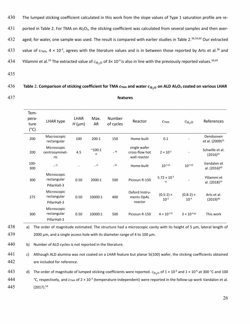
source separately. 330
a. Uncertainty over the fabrication of the conformality test chip. The uncertainty components of the LHAR chan-331
nels compared to an ideal roughness-free open channel with exact design dimensions are: (i) the real channel 332
22
height differs from the design height; (ii) the channel contains support pillars, which affect film growth; (iii) the 333
top membrane may bend inwards between the pillars and thereby decrease the channel height; (iv) at the en-334
trance into the LHAR channel in PillarHall-3, there is a nanostep of ca. 2 to 5 nm in height; and (v) there is roughness 335
at the bottom (and likely at the top) of the PillarHall-3 LHAR channel. 336
Related to (i), we estimate that during fabrication, tolerance for the oxide thickness that defines the channel 337
height was ± 10, 20, and 30 nm for 100, 500, and 2000 nm design channel heights, respectively. These numbers 338
were obtained from the thickness of silicon oxide measured during LHAR channel fabrication, as reported in Table 339
S5. Here, the relative uncertainty of the channel height is larger, the smaller the design height. There may also be 340
other, as yet unidentified factors that result in deviation of the real channel height from the design height; meas-341
urement of the real channel height is thus advisable. According to our estimation (Figure S10), for a channel height 342
of 500 nm, a 1% error in the channel height causes roughly a 1.5% error in the penetration depth. Related to (ii), 343
according to the analysis presented in Section 3.2 of the supporting information, for a 500 nm channel the effect 344
of pillars on the penetration depth will be less than 1% (Figure S11 and S12) for a typical pillar diameter of 4 µm 345
and an interdistance of 49 µm in a triangular symmetry. Related to (iii), according to the AFM measurements, in 346
the LHAR channel with 500 nm channel heights, the membrane bent to a displacement of ca. 25 nm (Figure S13 347
a). Bending was measured also for the 2000 nm design, and it was about the same as for the 500 nm design. The 348
100 nm design channel height bent ca. 40 nm (Figure S13 b). Related to (iv-v), the nanostep decreased the channel 349
height, and the roughness thereafter increased the surface area compared to the flat surface assumed in design 350
and modelling. Consequently, the apparent GPC increased (measured vertically), as the surface bound more mol-351
ecules per distance measurement unit than a completely flat surface would bind. Also, PD50% should be slightly 352
smaller and the slope at PD50% should be somewhat steeper than on a flat surface. 353
Concerning the fabrication-related uncertainty of the LHAR channels reported in this work, those with a design 354
channel height of 500 nm and pillar layout v1b succeeded best in reproducing the design target and are expected 355
to provide the most reliable saturation profile measurements. 356
23
b. Uncertainty related to the thickness measurement. For the reflectometry measurement, the uncertainty com-357
ponents stem from (i) manual placement of the sample for measurement, (ii) the optical thickness model behind 358
the reflectometry measurement, (iii) the referencing procedure of the reflectometry measurement (including 359
lamp aging), and (iv) motorized movement accuracy. Related to (i), in this work, the samples were manually posi-360
tioned to obtain the same starting position, compared to the entry under the membrane (Region II of Figure 3), 361
as that identified from visual microscope observation of the pillars and membrane remnants. We estimate this 362
positioning uncertainty to be on the order of 2 µm. Second, the samples were placed so that the line scan would 363
proceed inside the LHAR channel in exactly 90 angle compared to the channel entry. Deviation from 90 causes 364
a cosine error, which broadens the measured saturation profile and leads to a higher observed PD50%. In the pre-365
sent case, the cosine error is nevertheless estimated to be insignificant compared to the other uncertainty sources. 366
Related to (ii), the thickness measurement used in this work assumes a roughness-free film with constant thick-367
ness of a dielectric with the properties of ALD Al2O3 grown at 300C on a silicon surface. However, native oxide on 368
the silicon could have increased the measured thickness somewhat. Deviation of the optical model from reality 369
causes systematic error in the measured film thickness. Related to (iii), the challenges arose in the repeatability of 370
the reference measurement with reflectometer, especially at the high magnifications (preferably, 50X). Some-371
times, manual focusing was required to enable the measurement. By changing the reference, the measured film 372
thickness could change by some nanometers for a film of ca. 50 nm. 373
c. Uncertainty from the ALD process. Minor fluctuations occur in the ALD process during a run and run-to-run. 374
There are tolerances for flow rates, pressures, and temperatures alike. Moreover, at the beginning of ALD pro-375
cesses, a small deviation may occur in the reactant dose when a reactant bottle of an initially equilibrated vapor 376
pressure is taken into use, when the vapor pressure decreases, and if the vaporization kinetics are too slow enough 377
to saturate the gas during the period between two pulses. 378
The reproducibility of the saturation profile measurement can be visualized by comparing data from fully inde-379
pendent measurements of the TMA-water saturation profile at 300C, as done in Figure 8b. While there is varia-380
tion in the film thickness in the flat region and in the penetration depth, the overall saturation profile and the 381
24
slope at PD50% seem similar in all cases. Based on the data reported in Table 1 for samples 2, 4, 8, and 12, the 382
standard deviation of PD50% and the slope at PD50% were 19.4 µm and 0.0003 nm, respectively. The standard devi-383
ation of the initial film thickness in Region IIb was 2.8 nm. 384
B. Occasional spikes in the saturation profile 385
Spikes preceding the leading edge were occasionally observed in the saturation profiles (Figure 3). Schwille et 386
al.41 observed spikes in the saturation profile of TMA-water process measured with their MEMS-type conformality 387
test structures by ellipsometry. They proposed that a CVD-related phenomenon might have contributed to the 388
spikes.41 Interestingly, in our case, spikes were observed in the optical reflectometer measurement but not in SEM-389
EDS (Figure 5). 390
Detailed inspection revealed that the spikes appeared at locations where the measurement spot was close to 391
pillar remnants, see Figure S16. More spikes were observed in repeated reflectometer line scan of a sample having 392
the pillar layout design of v1a, which has a smaller pillar interdistance compared to v1b, see Figure S17. To create 393
reflectometer-based saturation profiles without pillar remnant influence and without spikes, it would be interest-394
ing to investigate the TMA-water process on LHAR channels with a less dense pillar network. Making such experi-395
ments is out of the scope of this work, however. 396
C. Insight into the characteristics of the TMA-water ALD process 397
Our work revealed, in accordance with Arts et al.,36 that TMA-limited and water-limited growth has different 398
characteristic shape of the saturation profile at 300 °C (Figure 11a). 399
The effect of purge time on the saturation profile of TMA-water ALD process was further investigated. Our re-400
sults showed an inverse dependency between the value of GPC and the purge length (Figure 11b and Figure S14). 401
We believe that during the longer purge, reversibly adsorbed water molecules could have desorbed, causing a 402
decrease in the concentration of surface OH groups. Consequently, the amount of TMA adsorbed decreased as 403
the amount of TMA adsorbed depends on the concentration of surface OH groups.13,50 Although the role of the 404
partly reversible water reaction has not been discussed in detail in the ALD literature, our findings are in line with 405
some earlier reports. Ylivaara et al.51 showed that GPC decreased as purge time increased (from 1 s to 4 s). Matero 406
25
et al.59 reported a higher GPC of the TMA-water ALD process for higher water partial pressure. Gakis et al.56 as-407
sumed reversible reaction of water. Sønsteby et al.26 noted that a long purge time can alter GPC due to dehydration 408
on the surface. 409
In our work, GPCI outside the channel decreased faster than GPCIIb inside the channel opening when the purge 410
time increased (Figure S14). Likely this can be explained by re-adsorption of the desorbed water on the channel 411
surface, leading to slower decrease in GPCIIb as a function of purge time compared to a planar surface. This con-412
clusion is in line with the analysis by Abelson and Girolami2 for desorption during CVD from a HAR feature. 413
The decrease in binding capacity of the surface towards TMA enabled the reactant molecules to penetrate 414
deeper into the channel before reacting, resulting in an increased penetration depth (Figure 11b). Increased pen-415
etration depth (in PillarHall-1) with decreased GPC has been observed in earlier works by Mattinen et al.47 for 416
iridium ALD and by Puurunen and Gao46 for Al2O3 ALD at different temperatures. 417
D. Sticking coefficients from saturation profile measurements 418
The method developed by Arts et al.36 allows one to calculate the lumped sticking coefficient of reactants from 419
Type 1 normalized saturation profile, provided that the growth is in the Knudsen flow regime. The calculation of 420
lumped sticking coefficient is made with Equation (3) of Arts et al.36: |d𝜃/d�̃�| ≈ √𝑐𝐴
13.9. To be in the Knudsen flow 421
regime, the molecule’s mean free path λ should be significantly larger than the characteristic size of the LHAR 422
structure h. In other words, Knudsen number Kn = λ/h ≫ 1. 423
To inform whether the Arts et al.36 method can be applied in this work, the mean free path λ was calculated. At 424
300 °C under the process conditions used in this work, the mean free path [calculated with Equation (3) Ref. 1] for 425
TMA and water is 40 and 100 µm, respectively. The characteristic size is interpreted as the hydraulic diameter of 426
the channel h, so that h = 2/(1/H+1/W). For a 500 nm channel, the hydraulic diameter is thus 1.0 µm, and the 427
Knudsen number is 40 and 100 for TMA and water, respectively. The Arts et al.36 method should thus be valid in 428
our case. 429
26
The lumped sticking coefficient calculated in this work from the slope values of Type 1 saturation profile are re-430
ported in Table 2. For TMA on Al2O3, the sticking coefficient was calculated from several samples and then aver-431
aged; for water, one sample was used. The result is compared with earlier studies in Table 2.36,54,60 Our extracted 432
value of cTMA, 4 × 10⁻³, agrees with the literature values and is in between those reported by Arts et al.36 and 433
Ylilammi et al.33 The extracted value of 𝑐H2O of 3× 10⁻⁴ is also in line with the previously reported values.36,60 434
435
Table 2. Comparison of sticking coefficient for TMA cTMA and water 𝒄𝐇𝟐𝐎 on ALD Al2O3 coated on various LHAR 436
features 437
Tem-pera-ture (°C)
LHAR type LHAR
H (µm) Max. AR
Number of cycles
Reactor cTMA 𝑐H2O References
200 Macroscopic rectangular
100 200:1 150 Home-built 0.1 - Dendooven
et al. (2009)31
200 Microscopic
centrosymmet-ric
4.5 ~100:1
a) - b)
single wafer cross-flow hot
wall reactor 2 × 10⁻² -
Schwille et al. (2016)41
100-300
- c) - - c) - b) Home-built 10-3 d) 10-4 d) Vandalon et al. (2016)60
300
Microscopic rectangular
PillarHall-3
0.50 2000:1 500 Picosun R-150 5.72 × 10⁻³
e) -
Ylilammi et al. (2018)33
275
Microscopic rectangular
PillarHall-3
0.50 10000:1 400 Oxford Instru-ments OpAL
reactor
(0.5-2) × 10-3
(0.8-2) × 10-4
Arts et al. (2019)36
300
Microscopic rectangular
PillarHall-3
0.50 10000:1 500 Picosun R-150 4 × 10⁻³ f) 3 × 10⁻⁴ g) This work
a) The order of magnitude estimated. The structure had a microscopic cavity with its height of 5 µm, lateral length of 438
2000 µm, and a single access hole with its diameter range of 4 to 100 µm. 439
b) Number of ALD cycles is not reported in the literature. 440
c) Although ALD alumina was not coated on a LHAR feature but planar Si(100) wafer, the sticking coefficients obtained 441
are included for reference. 442
d) The order of magnitude of lumped sticking coefficients were reported. 𝑐H2O of 1 × 10⁻⁴ and 1 × 10⁻⁶ at 300 °C and 100 443
°C, respectively, and cTMA of 2 × 10⁻³ (temperature-independent) were reported in the follow-up work Vandalon et al. 444
(2017).54 445
27
e) The alumina film density used by Ylilammi et al.33 was 4000 kg/m3 (not reported in the original publication33), which is 446
higher than in our study (3100 kg/m3). 447
f) Calculated for sample 2, 4, 8, and 12 by using Arts et al.36 method, and the results were averaged. 448
g) Calculated for sample 14 by using Arts et al.36 method. 449
F. Conclusions 450
This work created a benchmark for saturation profile based conformality analysis of ALD processes in rectangular 451
microscopic LHAR channels. As a test vehicle, the archetypical TMA-water process at the typical ALD temperature 452
of 300 °C was used. The effect of variations in LHAR structure prototype’s actual dimensions, effect of support 453
pillars on growth, the ALD process reproducibility, and the thickness measurement uncertainty were discussed. 454
Classifications and terminology related to saturation profile based conformality analysis were developed. The clas-455
sifications and terminology should be applicable to other LHAR-based saturation profile based conformality stud-456
ies of ALD and potentially, at least partly, also CVD and ALE studies. 457
The as-measured saturation profiles of thickness vs. distance differed for the TMA-water process, depending on 458
the number of cycles (250-1000) and the LHAR channel height employed (design height 100, 500, 2000 nm). The 459
saturation profiles approached the same values, when they were scaled with the number of ALD cycles and the 460
LHAR channel height. We propose the scaled saturation profile as an informative measure of an ALD process, 461
which at favorable conditions can become a characteristic fingerprint of an ALD process. Favorable conditions refer 462
at least to that gas-phase transport should be in the Knudsen diffusion regime and the LHAR channel should re-463
main sufficiently open (channel filling preferably less than 10%). 464
The saturation profile of ALD Al2O3 showed a near-ideal shape expected for an ALD process based on repeated 465
self-terminating gas-solid reactions, namely a constant thickness before a steep decrease to zero. The measured 466
saturation profile was not influenced by different lateral lengths of the LHAR channel (100 µm to 5 mm). Depend-467
ing on the magnitude of ALD reactant exposures, different limiting regimes can govern the ALD growth in LHAR 468
channels. With increasing TMA dose, the growth transformed from TMA-dose-limited to water-dose-limited. Con-469
trasting the ideality assumption of fully irreversible ALD reactions, we observed changes in the saturation profile 470
28
with increasing purge times. This observation can likely be related to a reversible component in the water reaction 471
with the TMA-modified surface in an ALD cycle. Lumped sticking coefficients calculated from the slope of the 472
saturation profile, agreed with previously reported values. 473
CONFLICTS OF INTEREST 474
R.L.P developed the concept of the microscopic LHAR conformality test and is the inventor of a related patent 475
application. VTT has made PillarHall™ test structure prototypes available for purchase. M.U. is responsible for 476
PillarHall™ test structure sales and commercialization activities at VTT and is the founder of Chipmetrics Oy. 477
ACKNOWLEDGMENT 478
R.L.P. acknowledges the expert help of colleagues at VTT Micronova, without whom the PillarHall-3 fabrication 479
would not have succeeded: MEMS processing learnings collection compiled by James Dekker; general advice from 480
Jaakko Saarilahti; valuable learnings from earlier PillarHall fabrication runs from Feng Gao; lithography mask draw-481
ing by Harri Pohjonen; supervising after R.L.P. of the PillarHall-3 fabrication by Mari Laamanen; and skillful clean 482
room fabrication from Meeri Partanen and Tuomo Honkaharju. J. Ruud van Ommen is thanked for his comments 483
on the manuscript. This work made use of Aalto University RawMatters and OtaNano infrastructures. The Pil-484
larHall-3 structures were first introduced, the influence of the pillars on film growth was analyzed and saturation 485
profile related terminology development was initiated at the EUROCVD21-Baltic ALD 15 conference, Linköping, 486
Sweden, June 11-14, 2017; at this conference, Angel Yanguas-Gil used the term “saturation profile”. The measure-487
ment spot size effect was first discussed at the AVS 17th International Conference on Atomic Layer Deposition 488
(ALD 2017), Denver, Colorado, July 15–18, 2017. The saturation profile data and simulations of this work were 489
introduced at the EuroCVD 22-Baltic ALD 16 Conference, Luxembourg, June 24–28, 2019. The uncertainty compo-490
nents were introduced at Nanoscale 2019, Braunschweig, Germany, October 15–16, 2019. The saturation profile 491
classification was proposed at the 66th AVS International Symposium and Exhibition, Columbus, Ohio, October 20–492
25, 2019. 493
Our experimental saturation profile data is planned to be uploaded to Zenodo for open access via https://ze-494
nodo.org/communities/ald-saturation-profile-open-data/. 495
29
Funding Sources 496
Funding for PillarHall-3 LHAR prototype fabrication at VTT was provided by the Academy of Finland via the Finnish 497
Centre of Excellence on Atomic Layer Deposition and via Tekes (currently: Business Finland) via the PillarHall TUTL 498
project. The work at Aalto University was supported by Puurunen’s starting grant and by the Academy of Finland 499
(COOLCAT consortium, decision no. 329978 and ALDI consortium, decision no. 331082). 500
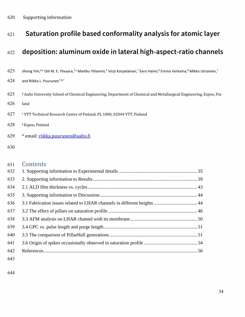
SYMBOLS AND ABBREVIATIONS 501
In this work, we have largely followed the notation of Ylilammi et al. 2018.33Additionally, we have taken influence 502
from Arts et al.36 503
a, distance between pillars (m); A, surface area (m2); 𝑐𝑇𝑀𝐴, lumped sticking coefficient of TMA; 𝑐𝐻2𝑂, lumped stick-504
ing coefficient of water; b, number of metal atoms in a molecule; d, pillar diameter (µm); 𝑑𝐴, molecular diameter 505
of Reactant A (pm); dB, molecular diameter of carrier gas B (pm); D, apparent diffusion coefficient (m2/s); D0, dif-506
fusion coefficient without pillars (m2/s); F, flux of material in direction x (mol/m2s); GPC, growth per cycle (m); 507
gpcsat, saturation growth in cycle (nm); H, channel height (nm); h, hydraulic diameter (µm); K, adsorption equilib-508
rium constant (1/Pa); Kn, Knudsen number (-); L, lateral length of the channel (µm); l, distance between rows of 509
pillars (µm); MB, molar mass of carrier gas B (kg/mol); MA, molar mass of reactant A (kg/mol); N, number of cycles; 510
𝑝𝐴0, input partial pressure of Reactant A (Pa); 𝑝𝐵, partial pressure of carrier gas B (Pa); PD50%, penetration depth 511
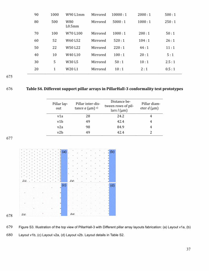
at 50% of film thickness (µm); Pd, desorption probability in unit time (1/s); Q, collision rate at unit pressure (m-2s-512
1Pa-1); q, adsorption density of reactant A at saturation (1/m2); R, diffusion resistance of a rectangular channel 513
(s/m3); Rrow, diffusion resistance of one row of pillars (s/m3); SI, film thickness outside the channel (m); SII, film 514
thickness inside the channel (m); tP, pulse length (s); W, opening width of the channel (m); x, distance from channel 515
opening (m); 𝑥50%, 50% thickness penetration depth (µm); �̃�, dimensionless distance (-); λTMA, mean free path of 516
TMA (µm); 𝜌, film density (kg/m3); 𝜃, surface coverage (0 𝜃 1); ξ, normalized distance (-). 517
518
AUTHOR INFORMATION 519
30
Corresponding Author 520
* email: [email protected], tel: +358 50 337 8161 521
522
REFERENCES 523
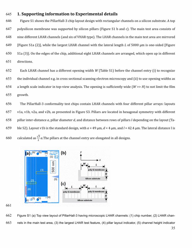
1 V. Cremers, R. L. Puurunen and J. Dendooven, Appl. Phys. Rev., 2019, 6, 021302. 524
2 J. R. Abelson and G. S. Girolami, J. Vac. Sci. Technol. A, 2020, 38, 030802. 525
3 A. van Asten, F. Roozeboom, R. Knaapen, P. Poodt and A. Illiberi, J. Vac. Sci. Technol. A Vacuum, Surfaces, 526
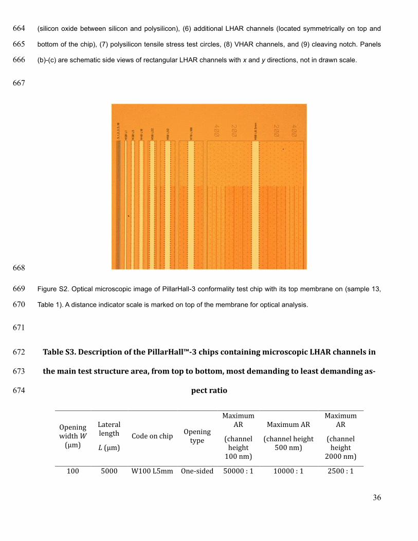
Film., 2011, 30, 01A142. 527
4 H. G. Kim and H. B. R. Lee, Chem. Mater., 2017, 29, 3809–3826. 528
5 P. Munnik, P. E. De Jongh and K. P. De Jong, Chem. Rev., 2015, 115, 6687–6718. 529
6 B. J. O’Neill, D. H. K. Jackson, J. Lee, C. Canlas, P. C. Stair, C. L. Marshall, J. W. Elam, T. F. Kuech, J. A. Dumesic 530
and G. W. Huber, ACS Catal., 2015, 5, 1804–1825. 531
7 T. Onn, R. Küngas, P. Fornasiero, K. Huang and R. Gorte, Inorganics, 2018, 6, 34. 532
8 P. Voigt, E. Haimi, J. Lahtinen, Y. W. Cheah, E. Mäkelä, T. Viinikainen and R. L. Puurunen, Top. Catal., 2019, 533
62, 611–620. 534
9 O. Graniel, M. Weber, S. Balme, P. Miele and M. Bechelany, Biosens. Bioelectron., 2018, 122, 147–159. 535
10 P. Poodt, A. Lankhorst, F. Roozeboom, K. Spee, D. Maas and A. Vermeer, Adv. Mater., 2010, 22, 3564–536
3567. 537
11 A. S. Asundi, J. A. Raiford and S. F. Bent, ACS Energy Lett., 2019, 4, 908–925. 538
12 M. Ritala and M. Leskelä, in Handbook of Thin Films Materials : Deposition and Processing of Thin Films, 539
ed. H. S. Nalwa, Academic Press, 2002, pp. 103–159. 540
13 R. L. Puurunen, J. Appl. Phys., 2005, 97, 121301. 541
14 M. G. Steven, Chem. Rev., 2010, 110, 111–131. 542
15 H. Van Bui, F. Grillo and J. R. Van Ommen, Chem. Commun., 2017, 53, 45–71. 543
16 FIN 52359, U.S. patent 4 058 430 (25 November 1975), 1974. 544
31
17 R. L. Puurunen, Chem. Vap. Depos., 2014, 20, 332–344. 545
18 G. N. Parsons, J. W. Elam, S. M. George, S. Haukka, H. Jeon, W. M. M. (Erwin) Kessels, M. Leskelä, P. Poodt, 546
M. Ritala and S. M. Rossnagel, J. Vac. Sci. Technol. A, 2013, 31, 050818. 547
19 G. N. Parsons, J. W. Elam, S. M. George, S. Haukka, H. Jeon, W. M. M. (Erwin) Kessels, M. Leskelä, P. Poodt, 548
M. Ritala and S. M. Rossnagel, J. Vac. Sci. Technol. A, 2020, 38, 037001. 549
20 V. B. Aleskovskii and S. I. Koltsov, Abstract of Scientific and Technical Conference, Goskhimizdat, Leningrad 550
1965, 67 (in Russian). 551
21 A. A. Malygin, V. E. Drozd, A. A. Malkov and V. M. Smirnov, Chem. Vap. Depos., 2015, 21, 216–240. 552
22 E. Ahvenniemi, A. R. Akbashev, S. Ali, M. Bechelany, M. Berdova, S. Boyadjiev, D. C. Cameron, R. Chen, M. 553
Chubarov, V. Cremers, A. Devi, V. Drozd, L. Elnikova, G. Gottardi, K. Grigoras, D. M. Hausmann, C. S. Hwang, 554
S.-H. Jen, T. Kallio, J. Kanervo, I. Khmelnitskiy, D. H. Kim, L. Klibanov, Y. Koshtyal, A. O. I. Krause, J. Kuhs, I. 555
Kärkkänen, M.-L. Kääriäinen, T. Kääriäinen, L. Lamagna, A. A. Łapicki, M. Leskelä, H. Lipsanen, J. Lyytinen, 556
A. Malkov, A. Malygin, A. Mennad, C. Militzer, J. Molarius, M. Norek, Ç. Özgit-Akgün, M. Panov, H. 557
Pedersen, F. Piallat, G. Popov, R. L. Puurunen, G. Rampelberg, R. H. A. Ras, E. Rauwel, F. Roozeboom, T. 558
Sajavaara, H. Salami, H. Savin, N. Schneider, T. E. Seidel, J. Sundqvist, D. B. Suyatin, T. Törndahl, J. R. van 559
Ommen, C. Wiemer, O. M. E. Ylivaara and O. Yurkevich, J. Vac. Sci. Technol. A, 2017, 35, 010801. 560
23 D. Cord, Finnish Physicist Tuomo Suntola Wins Millennium Technology Prize, https://finland.fi/business-561
innovation/finnish-physicist-tuomo-suntola-wins-millennium-technology-prize/, (accessed 12 December 562
2019). 563
24 J. W. Elam, D. Routkevitch, P. P. Mardilovich and M. G. Steven, Chem. Mater., 2003, 15, 3507–3517. 564
25 N. E. Richey, C. De Paula and S. F. Bent, J. Chem. Phys., 2020, 152, 040902. 565
26 H. H. Sønsteby, A. Yanguas-gil, J. W. Elam and J. W. Elam, J. Vac. Sci. Technol. A, 2020, 38, 020804. 566
27 A. Yanguas-Gil, Growth and Transport in Nanostructured Materials: Reactive Transport in PVD, CVD, and 567
ALD, Springer, 2016. 568
28 H. C. M. Knoops, E. Langereis, M. C. M. van de Sanden and W. M. M. Kessels, J. Electrochem. Soc., 2010, 569
32
157, G241–G249. 570
29 R. G. Gordon, D. Hausmann, E. Kim and J. Shepard, Chem. Vap. Depos., 2003, 9, 73–78. 571
30 M. C. Schwille, T. Schössler, J. Barth, M. Knaut, F. Schön, A. Höchst, M. Oettel and J. W. Bartha, J. Vac. Sci. 572
Technol. A Vacuum, Surfaces, Film., 2016, 35, 01B118. 573
31 J. Dendooven, D. Deduytsche, J. Musschoot, R. L. Vanmeirhaeghe and C. Detavernier, J. Electrochem. Soc., 574
2009, 156, P63–P67. 575
32 A. Yanguas-Gil and J. W. Elam, Chem. Vap. Depos., 2012, 18, 46–52. 576
33 M. Ylilammi, O. M. E. Ylivaara and R. L. Puurunen, J. Appl. Phys., 2018, 123, 205301. 577
34 P. Poodt, A. Mameli, J. Schulpen, W. M. M. (Erwin) Kessels and F. Roozeboom, J. Vac. Sci. Technol. A, 2017, 578
35, 021502. 579
35 M. Rose and J. W. Bartha, Appl. Surf. Sci., 2009, 255, 6620–6623. 580
36 K. Arts, V. Vandalon, R. L. Puurunen, M. Utriainen, F. Gao, W. M. M. Kessels and H. C. M. Knoops, J. Vac. 581
Sci. Technol. A, 2019, 37, 030908. 582
37 K. E. Elers, T. Blomberg, M. Peussa, B. Aitchison, S. Haukka and S. Marcus, Chem. Vap. Depos., 2006, 12, 583
13–24. 584
38 M. Ladanov, P. Algarin-Amaris, G. Matthews, M. Ram, S. Thomas, A. Kumar and J. Wang, Nanotechnology, 585
2013, 24, 375301. 586
39 J. Dendooven, D. Deduytsche, J. Musschoot, R. L. Vanmeirhaeghe and C. Detavernier, J. Electrochem. Soc., 587
2010, 157, G111–G116. 588
40 F. Gao, S. Arpiainen and R. L. Puurunen, J. Vac. Sci. Technol. A, 2015, 33, 010601. 589
41 M. C. Schwille, T. Schössler, F. Schön, M. Oettel and J. W. Bartha, J. Vac. Sci. Technol. A Vacuum, Surfaces, 590
Film., 2017, 35, 01B119. 591
42 A. M. Kia, N. Haufe, S. Esmaeili, C. Mart, M. Utriainen, R. L. Puurunen and W. Weinreich, Nanomaterials, 592
2019, 9, 1035. 593
43 L. Souqui, H. Högberg and H. Pedersen, Chem. Mater., 2019, 31, 5408–5412. 594
33
44 K. Arts, M. Utriainen, R. L. Puurunen, W. M. M. E. Kessels and H. C. M. Knoops, J. Phys. Chem. C, 2019, 1–595
11. 596
45 V. Miikkulainen, M. Leskelä, M. Ritala and R. L. Puurunen, J. Appl. Phys., 2013, 113, 021301. 597
46 R. L. Puurunen and F. Gao, 14th Int. Balt. Conf. At. Layer Depos. (BALD), St. Petersbg., 2016, 20–24. 598
47 M. Mattinen, J. Hämäläinen, F. Gao, P. Jalkanen, K. Mizohata, J. Räisänen, R. L. Puurunen, M. Ritala and M. 599
Leskelä, Langmuir, 2016, 32, 10559–10569. 600
48 K. Arts, J. H. Deijkers, T. Faraz, R. L. Puurunen, W. M. M. E. Kessels and H. C. M. Knoops, Appl. Phys. Lett., 601
2020, 117, 031602. 602
49 M. J. Young, A. Yanguas-gil, S. Letourneau, M. Coile, D. Mandia, M. Bedford, B. Aoun, A. S. Cavanagh, S. M. 603
George and J. W. Elam, ACS Appl. Mater. Interfaces, 2020, 1–22. 604
50 R. L. Puurunen, Appl. Surf. Sci., 2005, 245, 6–10. 605
51 O. M. E. Ylivaara, X. Liu, L. Kilpi, J. Lyytinen, D. Schneider, M. Laitinen, J. Julin, S. Ali, S. Sintonen, M. Berdova, 606
E. Haimi, T. Sajavaara, H. Ronkainen, H. Lipsanen, J. Koskinen, S.-P. Hannula and R. L. Puurunen, Thin Solid 607
Films, 2014, 552, 124–135. 608
52 M. Shirazi and S. D. Elliott, Nanoscale, 2015, 7, 6311–6318. 609
53 T. Weckman and K. Laasonen, Phys. Chem. Chem. Phys., 2015, 17, 17322–17334. 610
54 V. Vandalon and W. M. M. (Erwin) Kessels, J. Vac. Sci. Technol. A, 2017, 35, 05C313. 611
55 J. M. Lownsbury, J. A. Gladden, C. T. Campbell, I. S. Kim and A. B. F. Martinson, Chem. Mater., 2017, 29, 612
8566–8577. 613
56 G. P. Gakis, H. Vergnes, E. Scheid, C. Vahlas, A. G. Boudouvis and B. Caussat, Chem. Eng. Sci., 2019, 195, 614
399–412. 615
57 B. A. Sperling, B. Kalanyan and J. E. Maslar, J. Phys. Chem. C, 2020, 124, 3410–3420. 616
58 A. Yanguas-Gil and J. W. Elam, J. Vac. Sci. Technol. A, 2012, 30, 01A159. 617
59 R. Matero, A. Rahtu, M. Ritala, M. Leskelä and T. Sajavaara, Thin Solid Films, 2000, 368, 1–7. 618
60 V. Vandalon and W. M. M. Kessels, Appl. Phys. Lett., 2016, 108, 011607. 619
34
Supporting information 620
Saturation profile based conformality analysis for atomic layer 621
deposition: aluminum oxide in lateral high-aspect-ratio channels 622
Jihong Yim,§,x Oili M. E. Ylivaara,†,x Markku Ylilammi,‡ Virpi Korpelainen,† Eero Haimi,§ Emma Verkama,§ Mikko Utriainen,† 623
and Riikka L. Puurunen*,§,† 624
§ Aalto University School of Chemical Engineering, Department of Chemical and Metallurgical Engineering, Espoo, Fin-625
land 626
† VTT Technical Research Centre of Finland, PL 1000, 02044 VTT, Finland 627
‡ Espoo, Finland 628
* email: [email protected] 629
630
Contents 631
1. Supporting information to Experimental details ................................................................. 35 632
2. Supporting information to Results ....................................................................................... 39 633
2.1 ALD film thickness vs. cycles ........................................................................................... 43 634
3. Supporting information to Discussion ................................................................................. 44 635
3.1 Fabrication issues related to LHAR channels in different heights .................................... 44 636
3.2 The effect of pillars on saturation profile .......................................................................... 46 637
3.3 AFM analysis on LHAR channel with its membrane ........................................................ 50 638
3.4 GPC vs. pulse length and purge length .............................................................................. 51 639
3.5 The comparison of PillarHall generations ......................................................................... 51 640
3.6 Origin of spikes occasionally observed in saturation profile ............................................ 54 641
References................................................................................................................................ 56 642
643
644
35
1. Supporting information to Experimental details 645
Figure S1 shows the PillarHall-3 chip layout design with rectangular channels on a silicon substrate. A top 646
polysilicon membrane was supported by silicon pillars (Figure S1 b and c). The main test area consists of 647
nine different LHAR channels (and six of VHAR type). The LHAR channels in the main test area are mirrored 648
[Figure S1a (2)], while the largest LHAR channel with the lateral length L of 5000 µm is one-sided [Figure 649
S1a (3)]. On the edges of the chip, additional eight LHAR channels are arranged, which open up in different 650
directions. 651
Each LHAR channel has a different opening width W (Table S1) before the channel entry (i) to recognize 652
the individual channel e.g. in cross sectional scanning electron microscopy and (ii) to use opening widths as 653
a length scale indicator in top-view analysis. The opening is sufficiently wide (W >> H) to not limit the film 654
growth. 655
The PillarHall-3 conformality test chips contain LHAR channels with four different pillar arrays: layouts 656
v1a, v1b, v2a, and v2b, as presented in Figure S3. Pillars are located in hexagonal symmetry with different 657
pillar inter-distance a, pillar diameter d, and distance between rows of pillars l depending on the layout (Ta-658
ble S2). Layout v1b is the standard design, with a = 49 µm, d = 4 µm, and l = 42.4 µm. The lateral distance l is 659
calculated as √3
2𝑎.The pillars at the channel entry are elongated in all designs. 660
661
Figure S1 (a) Top view layout of PillarHall-3 having microscopic LHAR channels: (1) chip number, (2) LHAR chan-662
nels in the main test area, (3) the largest LHAR test feature, (4) pillar layout indicator, (5) channel height indicator 663
36
(silicon oxide between silicon and polysilicon), (6) additional LHAR channels (located symmetrically on top and 664
bottom of the chip), (7) polysilicon tensile stress test circles, (8) VHAR channels, and (9) cleaving notch. Panels 665
(b)-(c) are schematic side views of rectangular LHAR channels with x and y directions, not in drawn scale. 666
667
668
Figure S2. Optical microscopic image of PillarHall-3 conformality test chip with its top membrane on (sample 13, 669
Table 1). A distance indicator scale is marked on top of the membrane for optical analysis. 670
671
Table S3. Description of the PillarHall™-3 chips containing microscopic LHAR channels in 672
the main test structure area, from top to bottom, most demanding to least demanding as-673
pect ratio 674
Opening width W
(µm)
Lateral length
L (µm)
Code on chip Opening
type
Maximum AR
(channel height
100 nm)
Maximum AR
(channel height 500 nm)
Maximum AR
(channel height
2000 nm)
100 5000 W100 L5mm One-sided 50000 : 1 10000 : 1 2500 : 1
37
90 1000 W90 L1mm Mirrored 10000 : 1 2000 : 1 500 : 1
80 500 W80 L0.5mm
Mirrored 5000 : 1 1000 : 1 250 : 1
70 100 W70 L100 Mirrored 1000 : 1 200 : 1 50 : 1
60 52 W60 L52 Mirrored 520 : 1 104 : 1 26 : 1
50 22 W50 L22 Mirrored 220 : 1 44 : 1 11 : 1
40 10 W40 L10 Mirrored 100 : 1 20 : 1 5 : 1
30 5 W30 L5 Mirrored 50 : 1 10 : 1 2.5 : 1
20 1 W20 L1 Mirrored 10 : 1 2 : 1 0.5 : 1
675
Table S4. Different support pillar arrays in PillarHall-3 conformality test prototypes 676
Pillar lay-out
Pillar inter-dis-tance a (µm) a)
Distance be-tween rows of pil-
lars l (µm)
Pillar diam-eter d (µm)
v1a 28 24.2 4
v1b 49 42.4 4
v2a 98 84.9 4
v2b 49 42.4 2
677
678
Figure S3. Illustration of the top view of PillarHall-3 with Different pillar array layouts fabrication: (a) Layout v1a, (b) 679
Layout v1b, (c) Layout v2a, (d) Layout v2b. Layout details in Table S2. 680
38
681
Table S5. List of prepared samples with their unique sample code used during the analysis 682
(and thus traceable) and TMA-water ALD sequences on PillarHall-3 at 300 °C (varied varia-683
bles bolded) 684
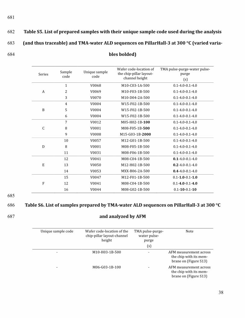
Series Sample
code Unique sample
code
Wafer code-location of the chip-pillar layout-
channel height
TMA pulse-purge-water pulse-purge
(s)
1 V0068 M10-C03-1A-500 0.1-4.0-0.1-4.0
A 2 V0069 M10-F03-1B-500 0.1-4.0-0.1-4.0
3 V0070 M10-D04-2A-500 0.1-4.0-0.1-4.0
4 V0004 W15-F02-1B-500 0.1-4.0-0.1-4.0
B 5 V0004 W15-F02-1B-500 0.1-4.0-0.1-4.0
6 V0004 W15-F02-1B-500 0.1-4.0-0.1-4.0
7 V0012 M05-H02-1B-100 0.1-4.0-0.1-4.0
C 8 V0001 M08-F05-1B-500 0.1-4.0-0.1-4.0
9 V0008 M15-G03-1B-2000 0.1-4.0-0.1-4.0
10 V0057 M12-G01-1B-500 0.1-4.0-0.1-4.0
D 8 V0001 M08-F05-1B-500 0.1-4.0-0.1-4.0
11 V0031 M08-F06-1B-500 0.1-4.0-0.1-4.0
12 V0041 M08-C04-1B-500 0.1-4.0-0.1-4.0
E 13 V0050 M12-H02-1B-500 0.2-4.0-0.1-4.0
14 V0053 MXX-B06-2A-500 0.4-4.0-0.1-4.0
15 V0047 M12-F01-1B-500 0.1-1.0-0.1-1.0
F 12 V0041 M08-C04-1B-500 0.1-4.0-0.1-4.0
16 V0044 M08-G02-1B-500 0.1-10-0.1-10
685
Table S6. List of samples prepared by TMA-water ALD sequences on PillarHall-3 at 300 °C 686
and analyzed by AFM 687
Unique sample code Wafer code-location of the chip-pillar layout-channel
height
TMA pulse-purge-water pulse-
purge
(s)
Note
- M10-H03-1B-500 - AFM measurement across the chip with its mem-brane on (Figure S13)
- M06-G03-1B-100 - AFM measurement across the chip with its mem-brane on (Figure S13)
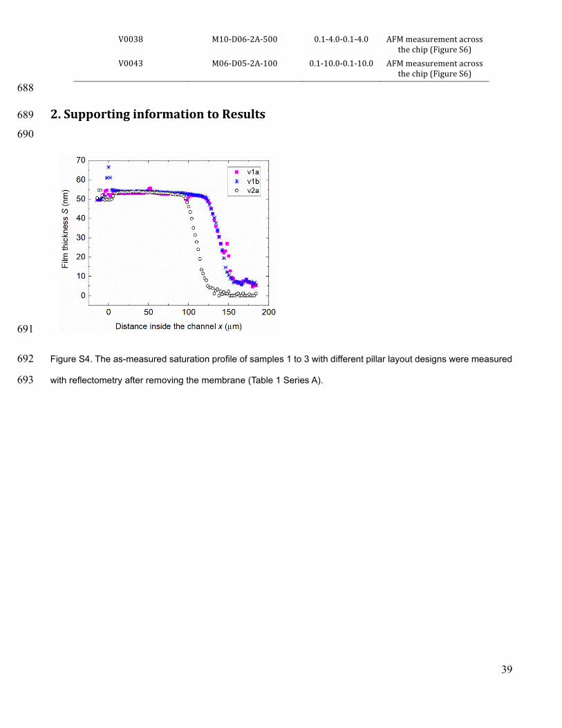
39
V0038 M10-D06-2A-500 0.1-4.0-0.1-4.0 AFM measurement across the chip (Figure S6)
V0043 M06-D05-2A-100 0.1-10.0-0.1-10.0 AFM measurement across the chip (Figure S6)
688
2. Supporting information to Results 689
690
691
Figure S4. The as-measured saturation profile of samples 1 to 3 with different pillar layout designs were measured 692
with reflectometry after removing the membrane (Table 1 Series A). 693
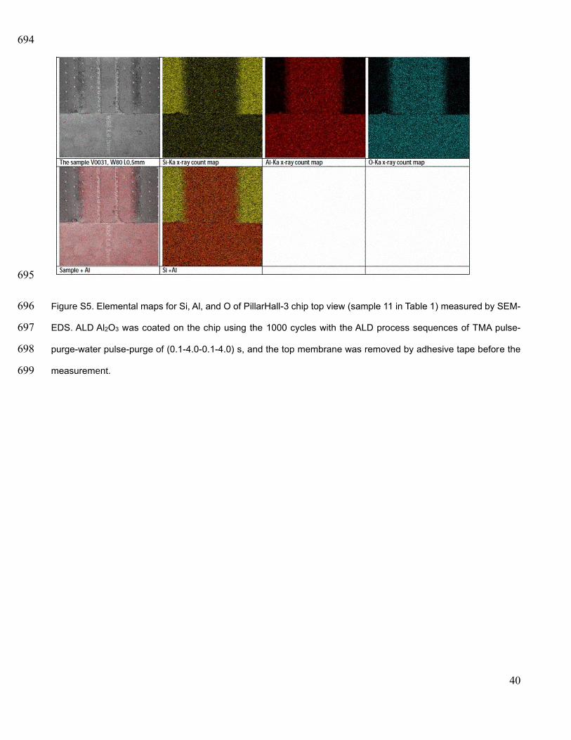
40
694
695
Figure S5. Elemental maps for Si, Al, and O of PillarHall-3 chip top view (sample 11 in Table 1) measured by SEM-696
EDS. ALD Al2O3 was coated on the chip using the 1000 cycles with the ALD process sequences of TMA pulse-697
purge-water pulse-purge of (0.1-4.0-0.1-4.0) s, and the top membrane was removed by adhesive tape before the 698
measurement. 699
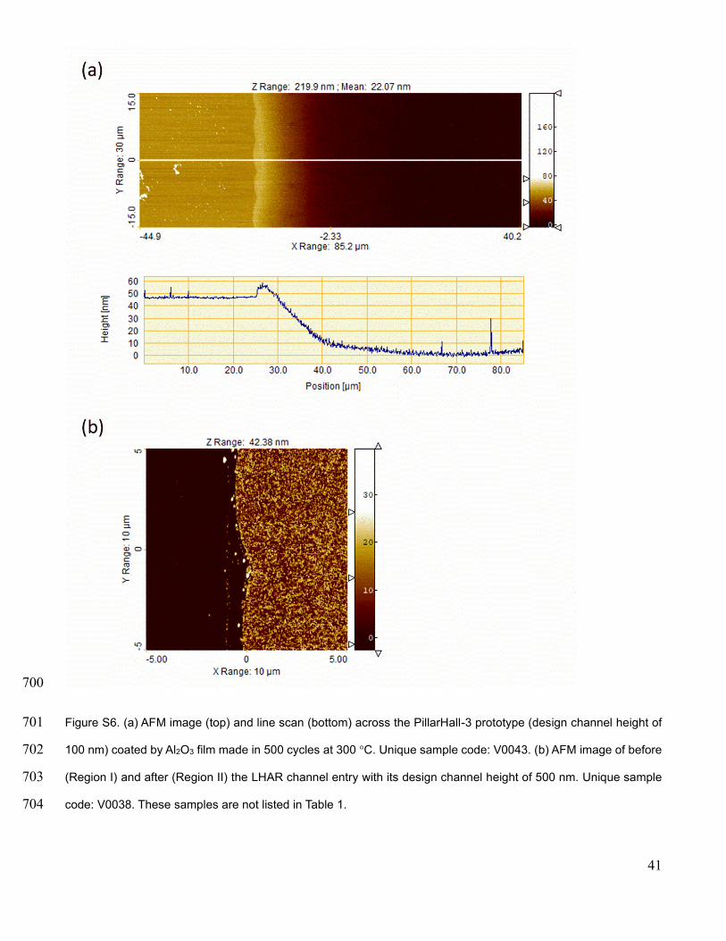
41
700
Figure S6. (a) AFM image (top) and line scan (bottom) across the PillarHall-3 prototype (design channel height of 701
100 nm) coated by Al2O3 film made in 500 cycles at 300 °C. Unique sample code: V0043. (b) AFM image of before 702
(Region I) and after (Region II) the LHAR channel entry with its design channel height of 500 nm. Unique sample 703
code: V0038. These samples are not listed in Table 1. 704
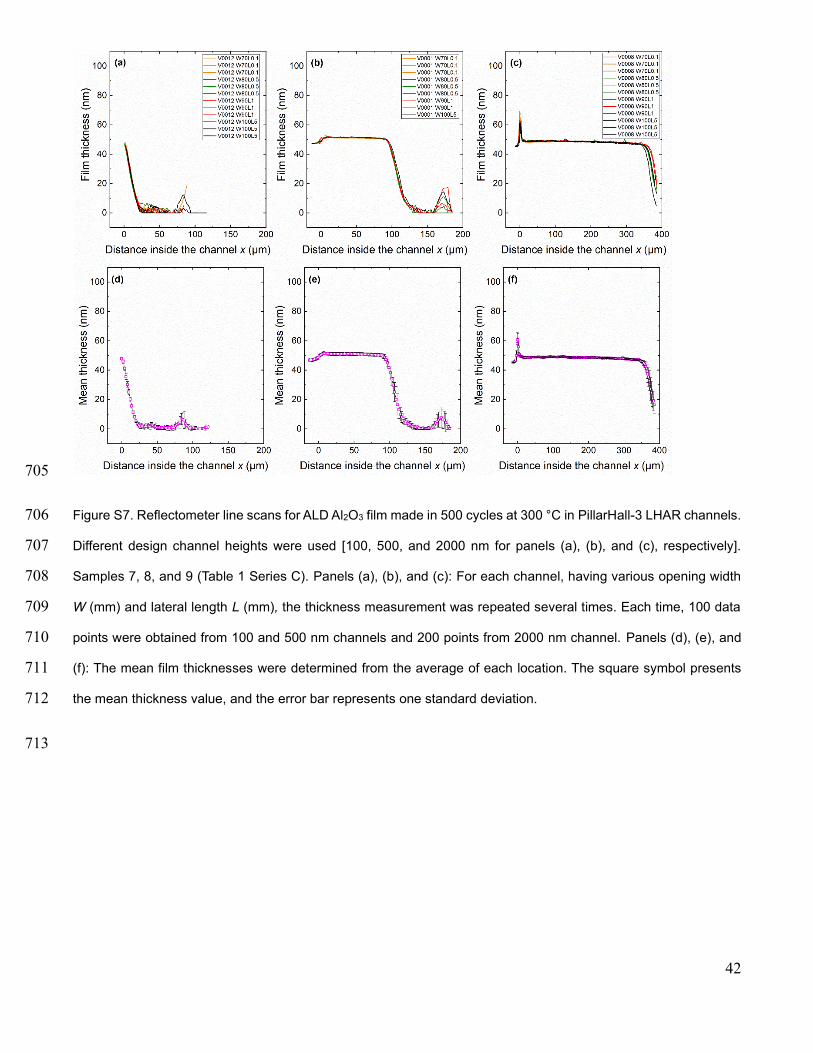
42
705
Figure S7. Reflectometer line scans for ALD Al2O3 film made in 500 cycles at 300 °C in PillarHall-3 LHAR channels. 706
Different design channel heights were used [100, 500, and 2000 nm for panels (a), (b), and (c), respectively]. 707
Samples 7, 8, and 9 (Table 1 Series C). Panels (a), (b), and (c): For each channel, having various opening width 708
W (mm) and lateral length L (mm), the thickness measurement was repeated several times. Each time, 100 data 709
points were obtained from 100 and 500 nm channels and 200 points from 2000 nm channel. Panels (d), (e), and 710
(f): The mean film thicknesses were determined from the average of each location. The square symbol presents 711
the mean thickness value, and the error bar represents one standard deviation. 712
713
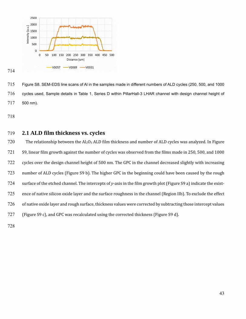
43
714
Figure S8. SEM-EDS line scans of Al in the samples made in different numbers of ALD cycles (250, 500, and 1000 715
cycles used, Sample details in Table 1, Series D within PillarHall-3 LHAR channel with design channel height of 716
500 nm). 717
718
2.1 ALD film thickness vs. cycles 719
The relationship between the Al2O3 ALD film thickness and number of ALD cycles was analyzed. In Figure 720
S9, linear film growth against the number of cycles was observed from the films made in 250, 500, and 1000 721
cycles over the design channel height of 500 nm. The GPC in the channel decreased slightly with increasing 722
number of ALD cycles (Figure S9 b). The higher GPC in the beginning could have been caused by the rough 723
surface of the etched channel. The intercepts of y-axis in the film growth plot (Figure S9 a) indicate the exist-724
ence of native silicon oxide layer and the surface roughness in the channel (Region IIb). To exclude the effect 725
of native oxide layer and rough surface, thickness values were corrected by subtracting those intercept values 726
(Figure S9 c), and GPC was recalculated using the corrected thickness (Figure S9 d). 727
728
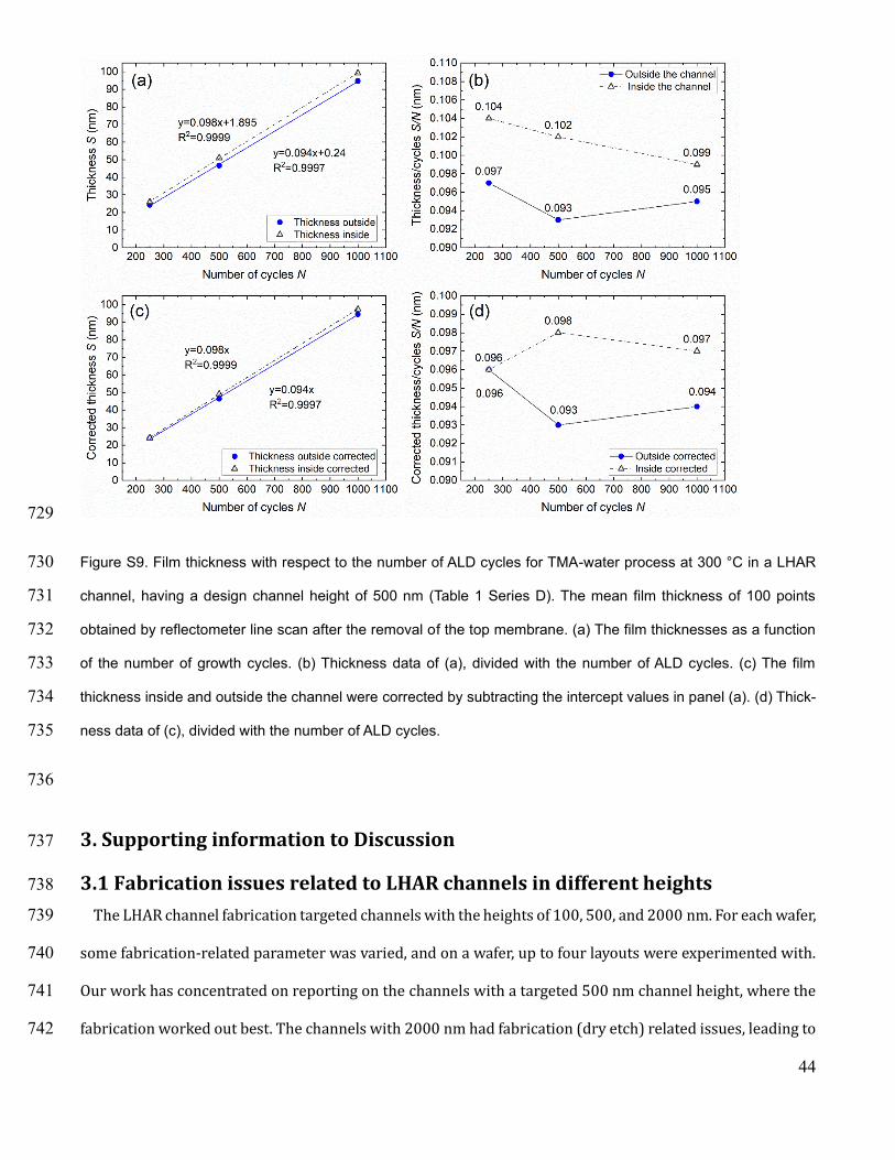
44
729
Figure S9. Film thickness with respect to the number of ALD cycles for TMA-water process at 300 °C in a LHAR 730
channel, having a design channel height of 500 nm (Table 1 Series D). The mean film thickness of 100 points 731
obtained by reflectometer line scan after the removal of the top membrane. (a) The film thicknesses as a function 732
of the number of growth cycles. (b) Thickness data of (a), divided with the number of ALD cycles. (c) The film 733
thickness inside and outside the channel were corrected by subtracting the intercept values in panel (a). (d) Thick-734
ness data of (c), divided with the number of ALD cycles. 735
736
3. Supporting information to Discussion 737
3.1 Fabrication issues related to LHAR channels in different heights 738
The LHAR channel fabrication targeted channels with the heights of 100, 500, and 2000 nm. For each wafer, 739
some fabrication-related parameter was varied, and on a wafer, up to four layouts were experimented with. 740
Our work has concentrated on reporting on the channels with a targeted 500 nm channel height, where the 741
fabrication worked out best. The channels with 2000 nm had fabrication (dry etch) related issues, leading to 742
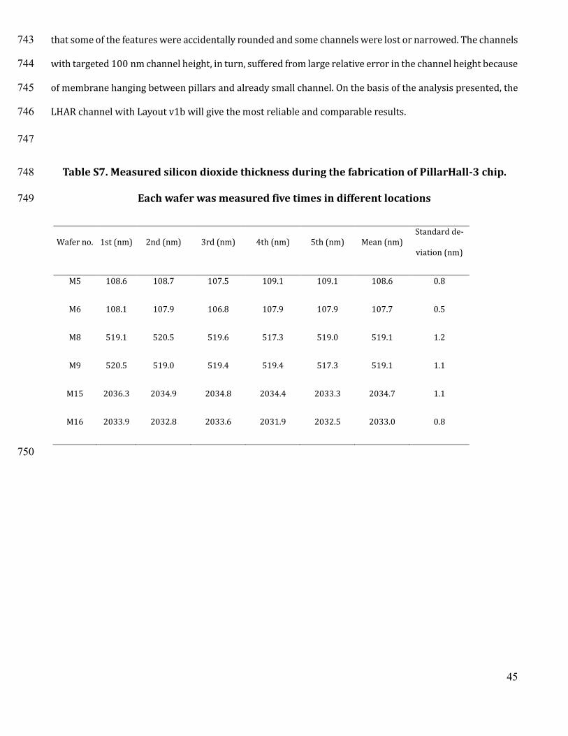
45
that some of the features were accidentally rounded and some channels were lost or narrowed. The channels 743
with targeted 100 nm channel height, in turn, suffered from large relative error in the channel height because 744
of membrane hanging between pillars and already small channel. On the basis of the analysis presented, the 745
LHAR channel with Layout v1b will give the most reliable and comparable results. 746
747
Table S7. Measured silicon dioxide thickness during the fabrication of PillarHall-3 chip. 748
Each wafer was measured five times in different locations 749
Wafer no. 1st (nm) 2nd (nm) 3rd (nm) 4th (nm) 5th (nm) Mean (nm) Standard de-
viation (nm)
M5 108.6 108.7 107.5 109.1 109.1 108.6 0.8
M6 108.1 107.9 106.8 107.9 107.9 107.7 0.5
M8 519.1 520.5 519.6 517.3 519.0 519.1 1.2
M9 520.5 519.0 519.4 519.4 517.3 519.1 1.1
M15 2036.3 2034.9 2034.8 2034.4 2033.3 2034.7 1.1
M16 2033.9 2032.8 2033.6 2031.9 2032.5 2033.0 0.8
750
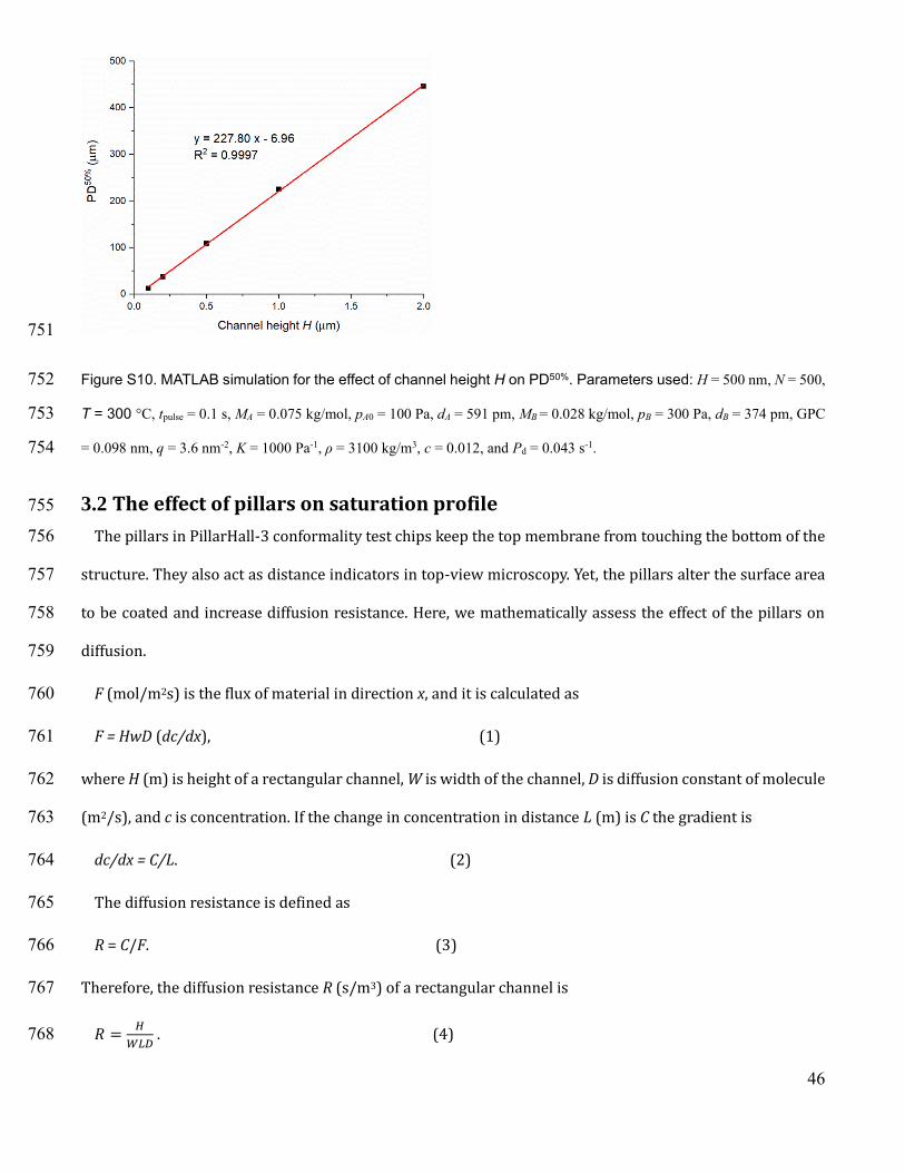
46
751
Figure S10. MATLAB simulation for the effect of channel height H on PD50%. Parameters used: H = 500 nm, N = 500, 752
T = 300 °C, tpulse = 0.1 s, MA = 0.075 kg/mol, pA0 = 100 Pa, dA = 591 pm, MB = 0.028 kg/mol, pB = 300 Pa, dB = 374 pm, GPC 753
= 0.098 nm, q = 3.6 nm-2, K = 1000 Pa-1, ρ = 3100 kg/m3, c = 0.012, and Pd = 0.043 s-1. 754
3.2 The effect of pillars on saturation profile 755
The pillars in PillarHall-3 conformality test chips keep the top membrane from touching the bottom of the 756
structure. They also act as distance indicators in top-view microscopy. Yet, the pillars alter the surface area 757
to be coated and increase diffusion resistance. Here, we mathematically assess the effect of the pillars on 758
diffusion. 759
F (mol/m2s) is the flux of material in direction x, and it is calculated as 760
F = HwD (dc/dx), (1) 761
where H (m) is height of a rectangular channel, W is width of the channel, D is diffusion constant of molecule 762
(m2/s), and c is concentration. If the change in concentration in distance L (m) is C the gradient is 763
dc/dx = C/L. (2) 764
The diffusion resistance is defined as 765
R = C/F. (3) 766
Therefore, the diffusion resistance R (s/m3) of a rectangular channel is 767
𝑅 =𝐻
𝑊𝐿𝐷 . (4) 768
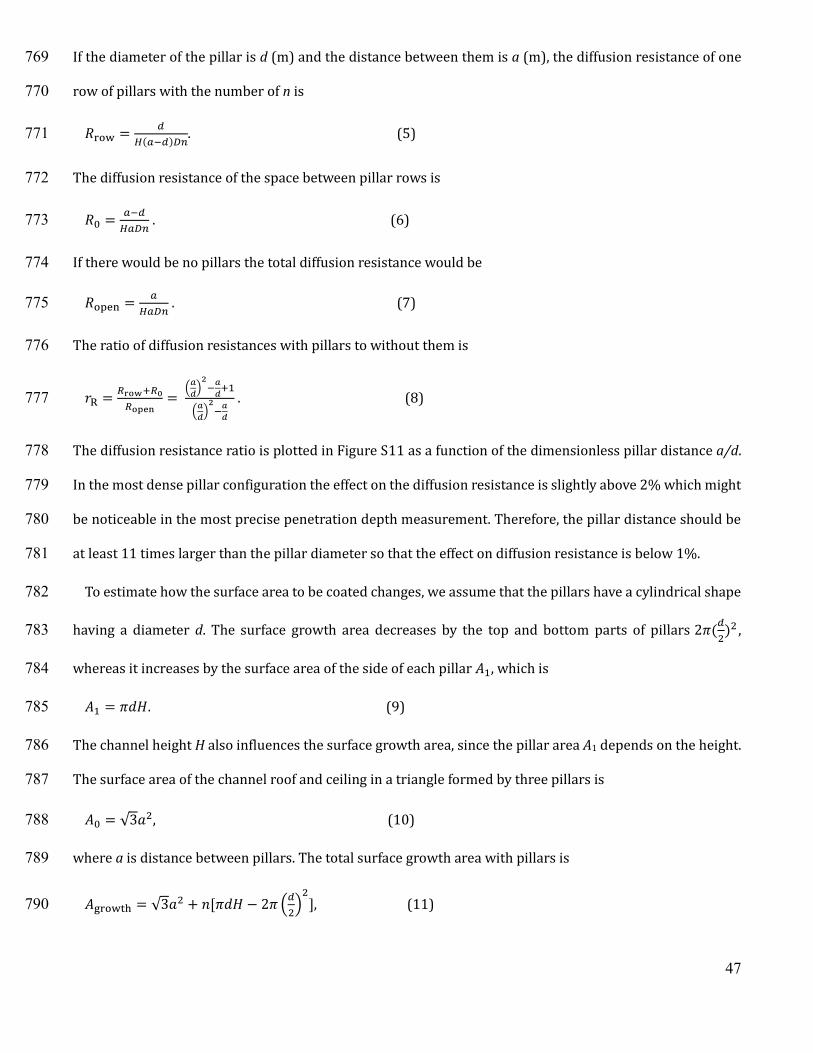
47
If the diameter of the pillar is d (m) and the distance between them is a (m), the diffusion resistance of one 769
row of pillars with the number of n is 770
𝑅row =𝑑
𝐻(𝑎−𝑑)𝐷𝑛. (5) 771
The diffusion resistance of the space between pillar rows is 772
𝑅0 =𝑎−𝑑
𝐻𝑎𝐷𝑛 . (6) 773
If there would be no pillars the total diffusion resistance would be 774
𝑅open =𝑎
𝐻𝑎𝐷𝑛 . (7) 775
The ratio of diffusion resistances with pillars to without them is 776
𝑟R =𝑅row+𝑅0
𝑅open=
(𝑎
𝑑)
2−
𝑎
𝑑+1
(𝑎
𝑑)
2−
𝑎
𝑑
. (8) 777
The diffusion resistance ratio is plotted in Figure S11 as a function of the dimensionless pillar distance a/d. 778
In the most dense pillar configuration the effect on the diffusion resistance is slightly above 2% which might 779
be noticeable in the most precise penetration depth measurement. Therefore, the pillar distance should be 780
at least 11 times larger than the pillar diameter so that the effect on diffusion resistance is below 1%. 781
To estimate how the surface area to be coated changes, we assume that the pillars have a cylindrical shape 782
having a diameter d. The surface growth area decreases by the top and bottom parts of pillars 2𝜋(𝑑
2)2 , 783
whereas it increases by the surface area of the side of each pillar 𝐴1, which is 784
𝐴1 = 𝜋𝑑𝐻. (9) 785
The channel height H also influences the surface growth area, since the pillar area A1 depends on the height. 786
The surface area of the channel roof and ceiling in a triangle formed by three pillars is 787
𝐴0 = √3𝑎2, (10) 788
where a is distance between pillars. The total surface growth area with pillars is 789
𝐴growth = √3𝑎2 + 𝑛[𝜋𝑑𝐻 − 2𝜋 (𝑑
2)
2], (11) 790
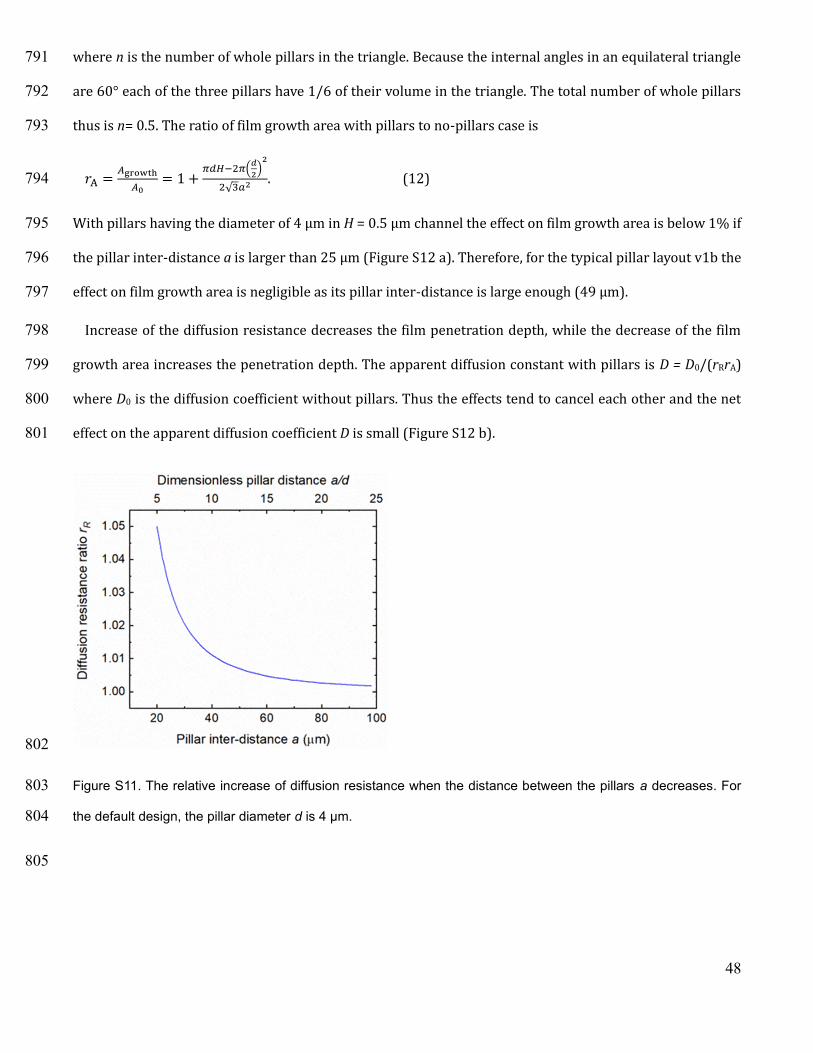
48
where n is the number of whole pillars in the triangle. Because the internal angles in an equilateral triangle 791
are 60° each of the three pillars have 1/6 of their volume in the triangle. The total number of whole pillars 792
thus is n= 0.5. The ratio of film growth area with pillars to no-pillars case is 793
𝑟A =𝐴growth
𝐴0= 1 +
𝜋𝑑𝐻−2𝜋(𝑑
2)
2
2√3𝑎2 . (12) 794
With pillars having the diameter of 4 μm in H = 0.5 μm channel the effect on film growth area is below 1% if 795
the pillar inter-distance a is larger than 25 μm (Figure S12 a). Therefore, for the typical pillar layout v1b the 796
effect on film growth area is negligible as its pillar inter-distance is large enough (49 µm). 797
Increase of the diffusion resistance decreases the film penetration depth, while the decrease of the film 798
growth area increases the penetration depth. The apparent diffusion constant with pillars is D = D0/(rRrA) 799
where D0 is the diffusion coefficient without pillars. Thus the effects tend to cancel each other and the net 800
effect on the apparent diffusion coefficient D is small (Figure S12 b). 801
802
Figure S11. The relative increase of diffusion resistance when the distance between the pillars a decreases. For 803
the default design, the pillar diameter d is 4 µm. 804
805
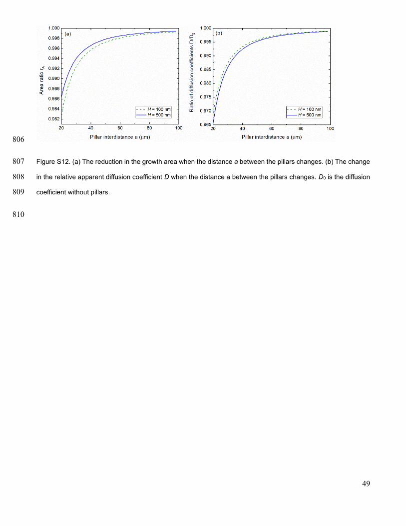
49
806
Figure S12. (a) The reduction in the growth area when the distance a between the pillars changes. (b) The change 807
in the relative apparent diffusion coefficient D when the distance a between the pillars changes. D0 is the diffusion 808
coefficient without pillars. 809
810
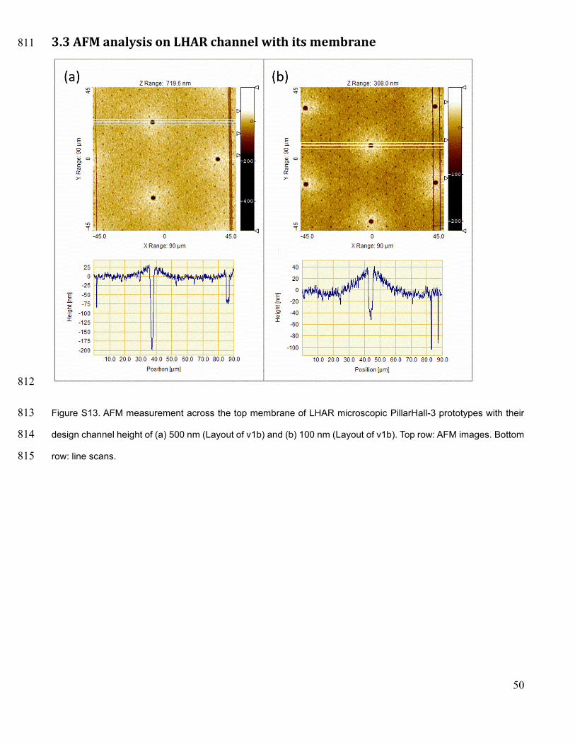
50
3.3 AFM analysis on LHAR channel with its membrane 811
812
Figure S13. AFM measurement across the top membrane of LHAR microscopic PillarHall-3 prototypes with their 813
design channel height of (a) 500 nm (Layout of v1b) and (b) 100 nm (Layout of v1b). Top row: AFM images. Bottom 814
row: line scans. 815
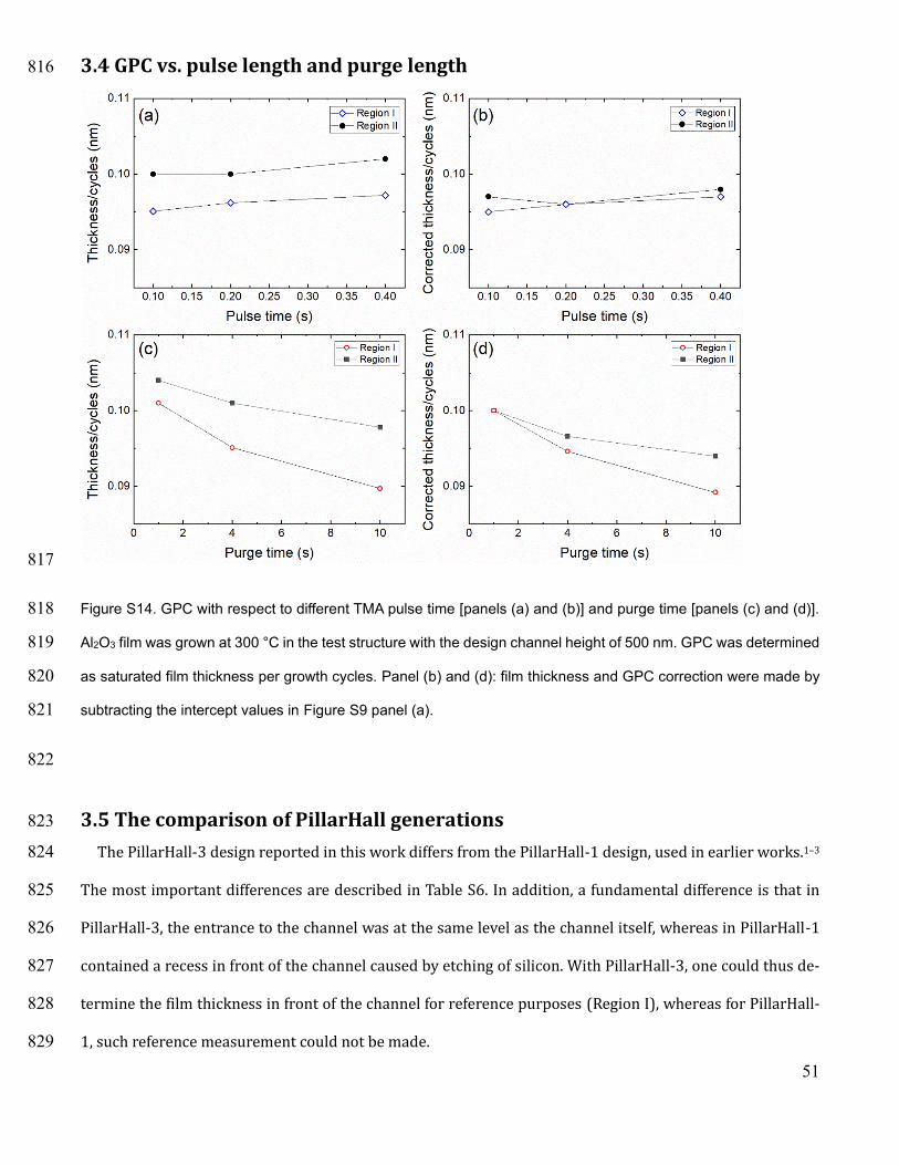
51
3.4 GPC vs. pulse length and purge length 816
817
Figure S14. GPC with respect to different TMA pulse time [panels (a) and (b)] and purge time [panels (c) and (d)]. 818
Al2O3 film was grown at 300 °C in the test structure with the design channel height of 500 nm. GPC was determined 819
as saturated film thickness per growth cycles. Panel (b) and (d): film thickness and GPC correction were made by 820
subtracting the intercept values in Figure S9 panel (a). 821
822
3.5 The comparison of PillarHall generations 823
The PillarHall-3 design reported in this work differs from the PillarHall-1 design, used in earlier works.1–3 824
The most important differences are described in Table S6. In addition, a fundamental difference is that in 825
PillarHall-3, the entrance to the channel was at the same level as the channel itself, whereas in PillarHall-1 826
contained a recess in front of the channel caused by etching of silicon. With PillarHall-3, one could thus de-827
termine the film thickness in front of the channel for reference purposes (Region I), whereas for PillarHall-828
1, such reference measurement could not be made. 829
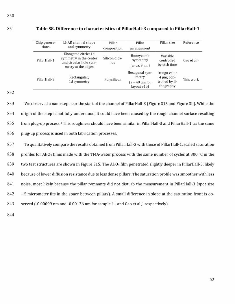
52
830
Table S8. Difference in characteristics of PillarHall-3 compared to PillarHall-1 831
Chip genera-tions
LHAR channel shape and symmetry
Pillar
composition
Pillar
arrangement
Pillar size Reference
PillarHall-1
Elongated circle; 1d symmetry in the center and circular hole sym-
metry at the edges
Silicon diox-ide
Honeycomb symmetry
(a=ca. 9 µm)
Variable controlled
by etch time Gao et al.1
PillarHall-3 Rectangular; 1d symmetry
Polysilicon
Hexagonal sym-metry
(a = 49 µm for layout v1b)
Design value 4 µm; con-
trolled by li-thography
This work
832
We observed a nanostep near the start of the channel of PillarHall-3 (Figure S15 and Figure 3b). While the 833
origin of the step is not fully understood, it could have been caused by the rough channel surface resulting 834
from plug-up process.4 This roughness should have been similar in PillarHall-3 and PillarHall-1, as the same 835
plug-up process is used in both fabrication processes. 836
To qualitatively compare the results obtained from PillarHall-3 with those of PillarHall-1, scaled saturation 837
profiles for Al2O3 films made with the TMA-water process with the same number of cycles at 300 °C in the 838
two test structures are shown in Figure S15. The Al2O3 film penetrated slightly deeper in PillarHall-3, likely 839
because of lower diffusion resistance due to less dense pillars. The saturation profile was smoother with less 840
noise, most likely because the pillar remnants did not disturb the measurement in PillarHall-3 (spot size 841
~5 micrometer fits in the space between pillars). A small difference in slope at the saturation front is ob-842
served (-0.00099 nm and -0.00136 nm for sample 11 and Gao et al.,1 respectively). 843
844
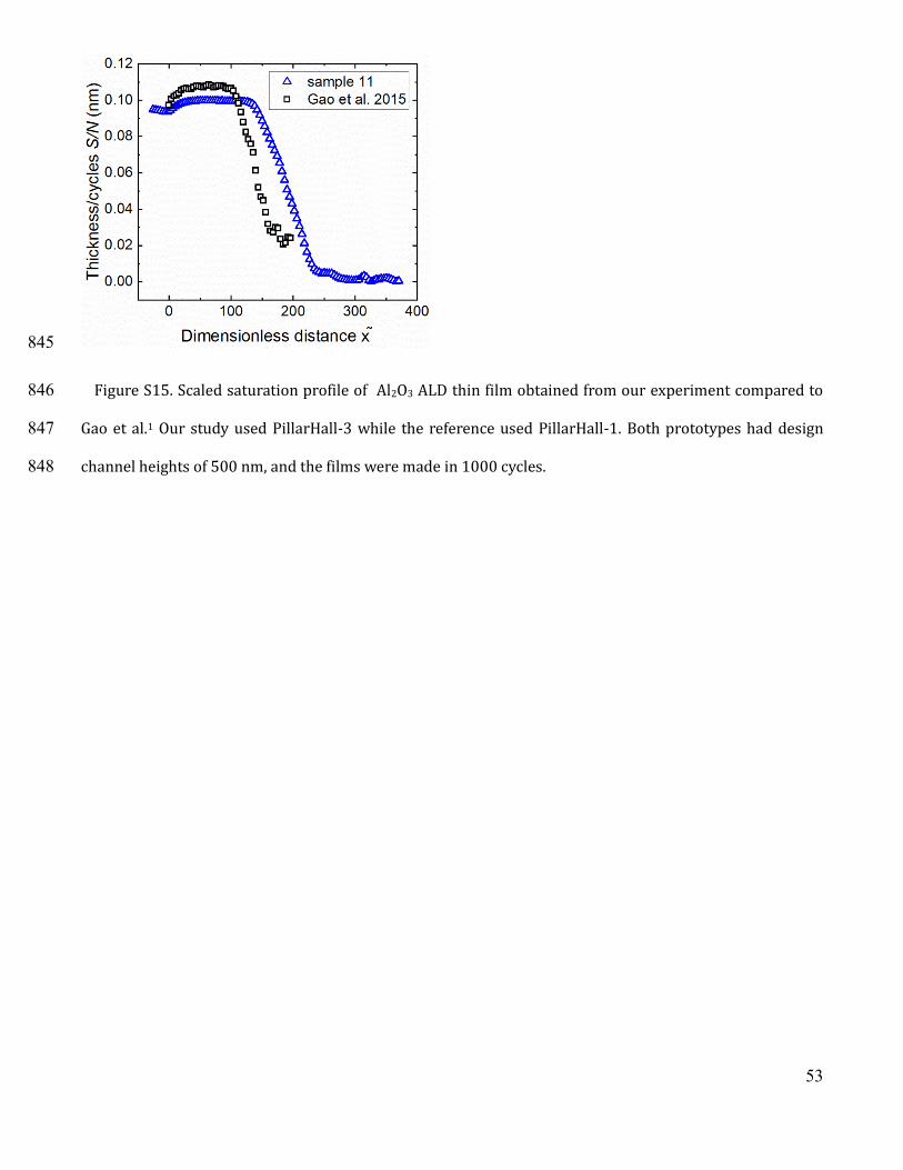
53
845
Figure S15. Scaled saturation profile of Al2O3 ALD thin film obtained from our experiment compared to 846
Gao et al.1 Our study used PillarHall-3 while the reference used PillarHall-1. Both prototypes had design 847
channel heights of 500 nm, and the films were made in 1000 cycles. 848
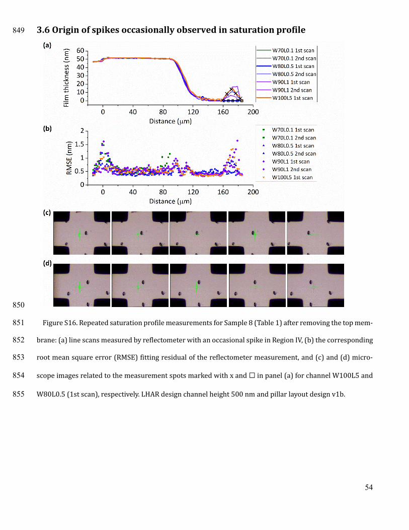
54
3.6 Origin of spikes occasionally observed in saturation profile 849
850
Figure S16. Repeated saturation profile measurements for Sample 8 (Table 1) after removing the top mem-851
brane: (a) line scans measured by reflectometer with an occasional spike in Region IV, (b) the corresponding 852
root mean square error (RMSE) fitting residual of the reflectometer measurement, and (c) and (d) micro-853
scope images related to the measurement spots marked with x and ☐ in panel (a) for channel W100L5 and 854
W80L0.5 (1st scan), respectively. LHAR design channel height 500 nm and pillar layout design v1b. 855
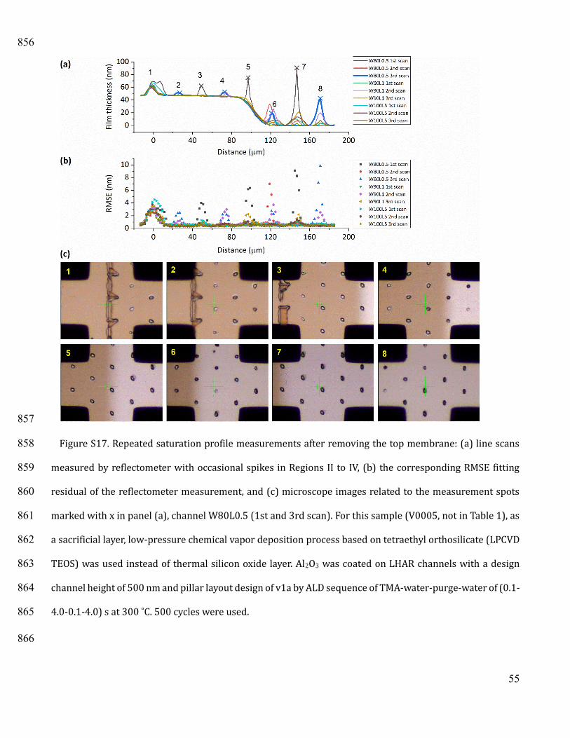
55
856
857
Figure S17. Repeated saturation profile measurements after removing the top membrane: (a) line scans 858
measured by reflectometer with occasional spikes in Regions II to IV, (b) the corresponding RMSE fitting 859
residual of the reflectometer measurement, and (c) microscope images related to the measurement spots 860
marked with x in panel (a), channel W80L0.5 (1st and 3rd scan). For this sample (V0005, not in Table 1), as 861
a sacrificial layer, low-pressure chemical vapor deposition process based on tetraethyl orthosilicate (LPCVD 862
TEOS) was used instead of thermal silicon oxide layer. Al2O3 was coated on LHAR channels with a design 863
channel height of 500 nm and pillar layout design of v1a by ALD sequence of TMA-water-purge-water of (0.1-864
4.0-0.1-4.0) s at 300 ˚C. 500 cycles were used. 865
866
56
References 867
1 F. Gao, S. Arpiainen and R. L. Puurunen, J. Vac. Sci. Technol. A, 2015, 33, 010601. 868
2 M. Mattinen, J. Hämäläinen, F. Gao, P. Jalkanen, K. Mizohata, J. Räisänen, R. L. Puurunen, M. Ritala 869
and M. Leskelä, Langmuir, 2016, 32, 10559–10569. 870
3 R. L. Puurunen and F. Gao, 14th Int. Balt. Conf. At. Layer Depos. (BALD), St. Petersbg., 2016, 20–24. 871
4 J. Kiihamäki, J. Dekker, P. Pekko, H. Kattelus and T. Mattila, Microsyst. Technol., 2004, 10, 346–350. 872
873

download fileview on ChemRxivJ.Y.and O.Y. et al._Chemrxiv_20200922.pdf (5.53 MiB)