Embed Size (px)
Citation preview
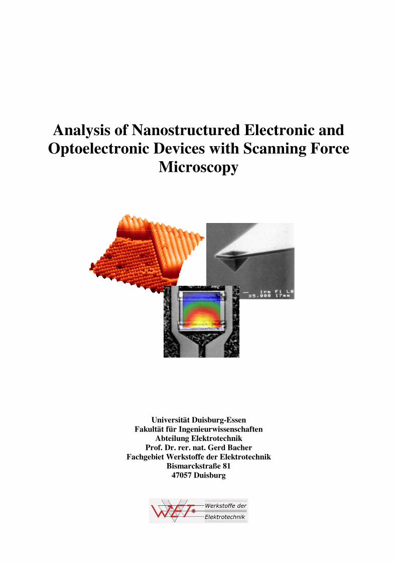
Analysis of Nanostructured Electronic and Optoelectronic Devices with Scanning Force
Microscopy
Universität Duisburg-Essen Fakultät für Ingenieurwissenschaften
Abteilung Elektrotechnik Prof. Dr. rer. nat. Gerd Bacher
Fachgebiet Werkstoffe der Elektrotechnik Bismarckstraße 81
47057 Duisburg
Introduction The Scanning Probe Microscopy (SPM) was invented in the early 1980’s. Now, SPMs are used in a wide variety of disciplines, including fundamental surface science, semiconductor technology, biology, or medicine. The SPM is an imaging tool with a vast dynamic range, spanning the realms of optical and electron microscopes. It is also a profiler with unprecedented 3-D resolution. Additionally, SPMs can measure physical properties such as surface conductivity, static charge distribution, light emission, magnetic fields, and heat dissipation. SPM covers a lateral range of imaging from several 100 μm to 10 pm. The SPM techniques can be divided into different categories, like e. g. Scanning Tunnelling Microscopy (STM), Scanning Nearfield Optical Microscopy (SNOM), Scanning Capacitance Microscopy (SCM), or Scanning Force Microscopy (SFM). In this laboratory exercise you will learn principles and some applications of SFM. At the end you are able to explain the functioning of the SFM in different operation modes. You will understand how electric and magnetic fields can be imaged. Additionally, you will be able to handle roughly such a Scanning Force Microscope and you will have performed different measurements on electronic or optoelectronic devices.
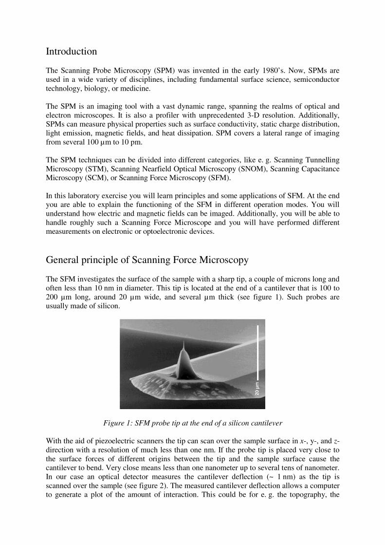
General principle of Scanning Force Microscopy The SFM investigates the surface of the sample with a sharp tip, a couple of microns long and often less than 10 nm in diameter. This tip is located at the end of a cantilever that is 100 to 200 μm long, around 20 μm wide, and several μm thick (see figure 1). Such probes are usually made of silicon.
Figure 1: SFM probe tip at the end of a silicon cantilever With the aid of piezoelectric scanners the tip can scan over the sample surface in x-, y-, and z-direction with a resolution of much less than one nm. If the probe tip is placed very close to the surface forces of different origins between the tip and the sample surface cause the cantilever to bend. Very close means less than one nanometer up to several tens of nanometer. In our case an optical detector measures the cantilever deflection (~ 1 nm) as the tip is scanned over the sample (see figure 2). The measured cantilever deflection allows a computer to generate a plot of the amount of interaction. This could be for e. g. the topography, the
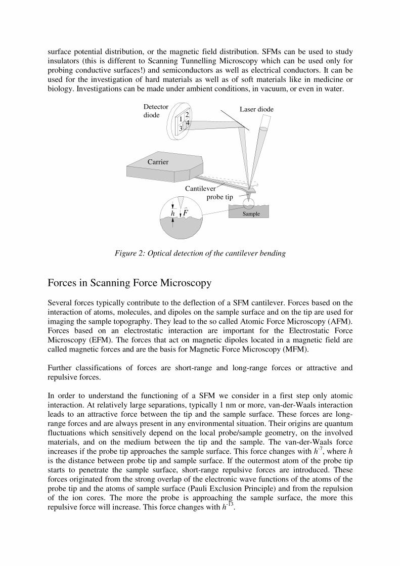
surface potential distribution, or the magnetic field distribution. SFMs can be used to study insulators (this is different to Scanning Tunnelling Microscopy which can be used only for probing conductive surfaces!) and semiconductors as well as electrical conductors. It can be used for the investigation of hard materials as well as of soft materials like in medicine or biology. Investigations can be made under ambient conditions, in vacuum, or even in water.
h F
12
34
Sample
Cantileverprobe tip
Carrier
Detector diode
Laser diode
Figure 2: Optical detection of the cantilever bending
Forces in Scanning Force Microscopy Several forces typically contribute to the deflection of a SFM cantilever. Forces based on the interaction of atoms, molecules, and dipoles on the sample surface and on the tip are used for imaging the sample topography. They lead to the so called Atomic Force Microscopy (AFM). Forces based on an electrostatic interaction are important for the Electrostatic Force Microscopy (EFM). The forces that act on magnetic dipoles located in a magnetic field are called magnetic forces and are the basis for Magnetic Force Microscopy (MFM). Further classifications of forces are short-range and long-range forces or attractive and repulsive forces. In order to understand the functioning of a SFM we consider in a first step only atomic interaction. At relatively large separations, typically 1 nm or more, van-der-Waals interaction leads to an attractive force between the tip and the sample surface. These forces are long-range forces and are always present in any environmental situation. Their origins are quantum fluctuations which sensitively depend on the local probe/sample geometry, on the involved materials, and on the medium between the tip and the sample. The van-der-Waals force increases if the probe tip approaches the sample surface. This force changes with h-7, where h is the distance between probe tip and sample surface. If the outermost atom of the probe tip starts to penetrate the sample surface, short-range repulsive forces are introduced. These forces originated from the strong overlap of the electronic wave functions of the atoms of the probe tip and the atoms of sample surface (Pauli Exclusion Principle) and from the repulsion of the ion cores. The more the probe is approaching the sample surface, the more this repulsive force will increase. This force changes with h-13.
The net force is the sum of the attractive and the repulsive forces. The resulting force can be roughly estimated by the simple Lennard-Jones-Model:
7
att13
repres h
k
h
kF −= (1)
The corresponding curve is shown in figure 3.
Figure 3: Force-distance-characteristic based on atomic interaction The net force exhibits first a point of inflection (non-contact region), then an absolute minimum, followed by a situation where the repulsive forces just balance the attractive forces. This point is at around 0.25 nm. Finally it shows a regime where the repulsive forces outdo the attractive ones (contact region). In this regime the probe tip seriously penetrate the sample surface, first leading to elastic and finally to inelastic deformations. These forces are used to image the topography of the sample. If there is a voltage between a conductive probe tip and the sample surface long-range electrostatic forces (Coulomb-forces) act between tip and sample. If one considers the tip-sample system as a capacitor with distance-dependent capacitance C, the force is given by
( )2sampleprobeel 2
1UU
h
CF −
∂∂= (2)
This equation is the basis for the Electric Force Microscopy with different sub-techniques like Kelvin Force Microscopy or Scanning Probe Voltage Measurement. The forces that act on magnetic dipoles located in a magnetic field are called magnetic forces. In force microscopy experiments, the magnetic dipoles are usually contained in the ferromagnetic material on/of the probe tip. The magnetic field is produced by a ferromagnetic sample (like a hard disc) or by an electrical current through an interconnection line inside an integrated circuit. The acting force between the tip and the magnetic field is
h
∫∫∫ ∂∂⋅=
tip i
sampletip0mag,i x
HMF
rr
μ (3)
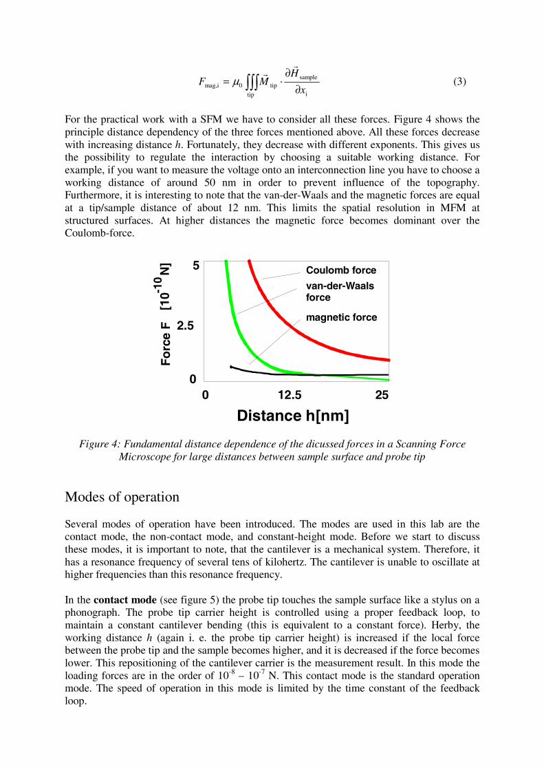
For the practical work with a SFM we have to consider all these forces. Figure 4 shows the principle distance dependency of the three forces mentioned above. All these forces decrease with increasing distance h. Fortunately, they decrease with different exponents. This gives us the possibility to regulate the interaction by choosing a suitable working distance. For example, if you want to measure the voltage onto an interconnection line you have to choose a working distance of around 50 nm in order to prevent influence of the topography. Furthermore, it is interesting to note that the van-der-Waals and the magnetic forces are equal at a tip/sample distance of about 12 nm. This limits the spatial resolution in MFM at structured surfaces. At higher distances the magnetic force becomes dominant over the Coulomb-force.
Distance h
Fo
rce
F
Coulomb force
van-der-Waalsforce
magnetic force
00
2.5
12.5
[nm]25
5
[10
N
]-1
0
Figure 4: Fundamental distance dependence of the dicussed forces in a Scanning Force Microscope for large distances between sample surface and probe tip
Modes of operation Several modes of operation have been introduced. The modes are used in this lab are the contact mode, the non-contact mode, and constant-height mode. Before we start to discuss these modes, it is important to note, that the cantilever is a mechanical system. Therefore, it has a resonance frequency of several tens of kilohertz. The cantilever is unable to oscillate at higher frequencies than this resonance frequency. In the contact mode (see figure 5) the probe tip touches the sample surface like a stylus on a phonograph. The probe tip carrier height is controlled using a proper feedback loop, to maintain a constant cantilever bending (this is equivalent to a constant force). Herby, the working distance h (again i. e. the probe tip carrier height) is increased if the local force between the probe tip and the sample becomes higher, and it is decreased if the force becomes lower. This repositioning of the cantilever carrier is the measurement result. In this mode the loading forces are in the order of 10-8 – 10-7 N. This contact mode is the standard operation mode. The speed of operation in this mode is limited by the time constant of the feedback loop.
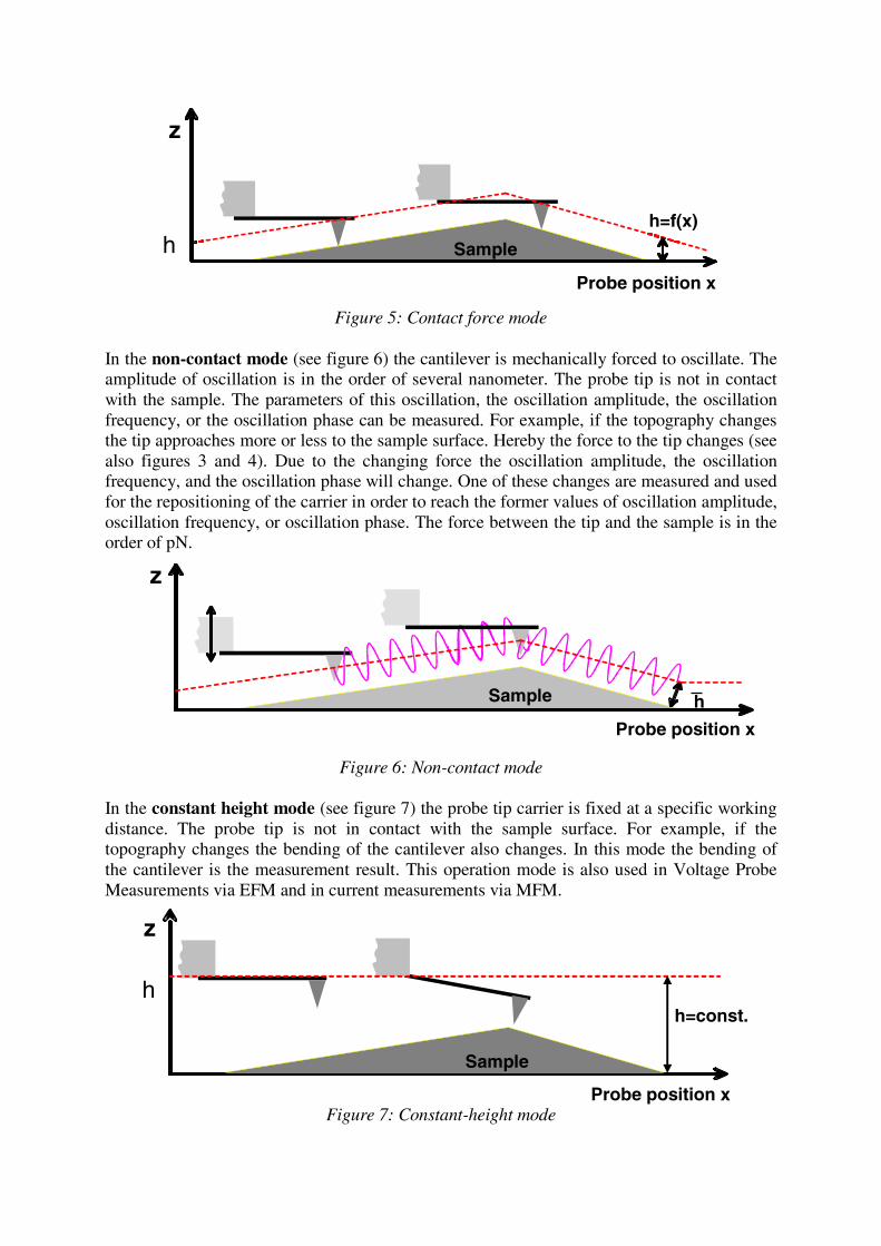
Figure 5: Contact force mode In the non-contact mode (see figure 6) the cantilever is mechanically forced to oscillate. The amplitude of oscillation is in the order of several nanometer. The probe tip is not in contact with the sample. The parameters of this oscillation, the oscillation amplitude, the oscillation frequency, or the oscillation phase can be measured. For example, if the topography changes the tip approaches more or less to the sample surface. Hereby the force to the tip changes (see also figures 3 and 4). Due to the changing force the oscillation amplitude, the oscillation frequency, and the oscillation phase will change. One of these changes are measured and used for the repositioning of the carrier in order to reach the former values of oscillation amplitude, oscillation frequency, or oscillation phase. The force between the tip and the sample is in the order of pN.
Figure 6: Non-contact mode In the constant height mode (see figure 7) the probe tip carrier is fixed at a specific working distance. The probe tip is not in contact with the sample surface. For example, if the topography changes the bending of the cantilever also changes. In this mode the bending of the cantilever is the measurement result. This operation mode is also used in Voltage Probe Measurements via EFM and in current measurements via MFM.
Figure 7: Constant-height mode
Probe position x
z
h=f(x)
Sample h
z
Sample
Probe position x
h
z
h
Probe position x
h=const.
Sample
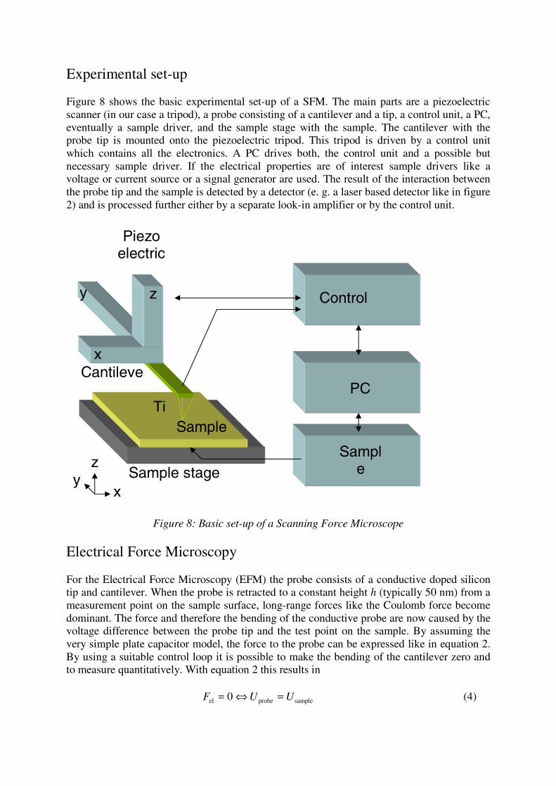
Experimental set-up Figure 8 shows the basic experimental set-up of a SFM. The main parts are a piezoelectric scanner (in our case a tripod), a probe consisting of a cantilever and a tip, a control unit, a PC, eventually a sample driver, and the sample stage with the sample. The cantilever with the probe tip is mounted onto the piezoelectric tripod. This tripod is driven by a control unit which contains all the electronics. A PC drives both, the control unit and a possible but necessary sample driver. If the electrical properties are of interest sample drivers like a voltage or current source or a signal generator are used. The result of the interaction between the probe tip and the sample is detected by a detector (e. g. a laser based detector like in figure 2) and is processed further either by a separate look-in amplifier or by the control unit.
Figure 8: Basic set-up of a Scanning Force Microscope
Electrical Force Microscopy For the Electrical Force Microscopy (EFM) the probe consists of a conductive doped silicon tip and cantilever. When the probe is retracted to a constant height h (typically 50 nm) from a measurement point on the sample surface, long-range forces like the Coulomb force become dominant. The force and therefore the bending of the conductive probe are now caused by the voltage difference between the probe tip and the test point on the sample. By assuming the very simple plate capacitor model, the force to the probe can be expressed like in equation 2. By using a suitable control loop it is possible to make the bending of the cantilever zero and to measure quantitatively. With equation 2 this results in
sampleprobeel 0 UUF =⇔= (4)
Control
Sample
Piezo electric
PC
Sample
x
y z
Cantileve
Ti
Sample stage x
y z
By measuring the free adjustable probe signal probeU the unknown sample signal sampleU can
be determined quantitatively. This method is known as the zero force method and is used e. g. for the Kelvin Force Microscopy or quantitative voltage signal measurements in electronic circuits. The spatial resolution for voltage measurements via Electrical Force Microscopy is less than 75 nm and the sensitivity is about 500 μV.
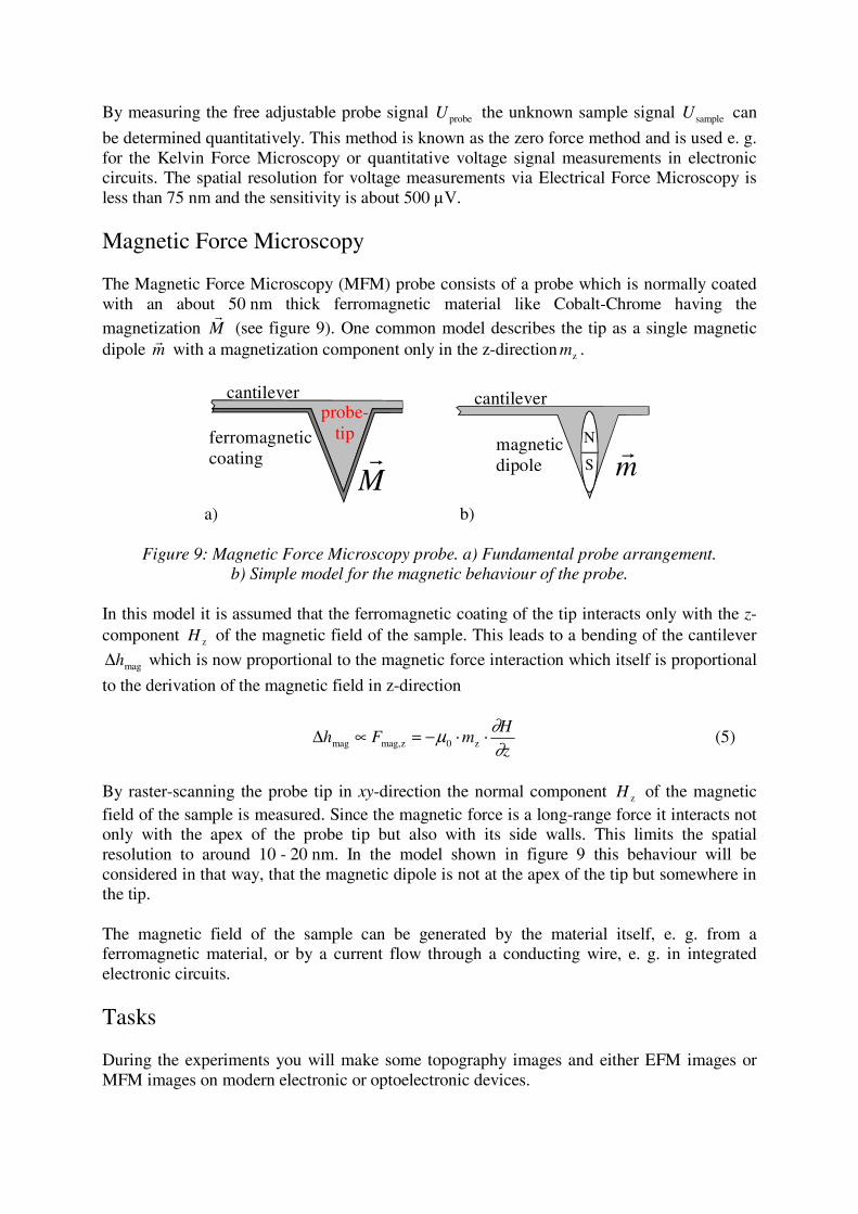
Magnetic Force Microscopy The Magnetic Force Microscopy (MFM) probe consists of a probe which is normally coated with an about 50 nm thick ferromagnetic material like Cobalt-Chrome having the magnetization M
r (see figure 9). One common model describes the tip as a single magnetic
dipole mr
with a magnetization component only in the z-direction zm .
cantilever
ferromagneticcoating
probe-tip
cantilever
N
S mrmagnetic
dipoleMr
a) b)
Figure 9: Magnetic Force Microscopy probe. a) Fundamental probe arrangement.
b) Simple model for the magnetic behaviour of the probe. In this model it is assumed that the ferromagnetic coating of the tip interacts only with the z-component zH of the magnetic field of the sample. This leads to a bending of the cantilever
maghΔ which is now proportional to the magnetic force interaction which itself is proportional
to the derivation of the magnetic field in z-direction
z
HmFh
∂∂μ ⋅⋅−=∝Δ z0zmag,mag (5)
By raster-scanning the probe tip in xy-direction the normal component zH of the magnetic field of the sample is measured. Since the magnetic force is a long-range force it interacts not only with the apex of the probe tip but also with its side walls. This limits the spatial resolution to around 10 - 20 nm. In the model shown in figure 9 this behaviour will be considered in that way, that the magnetic dipole is not at the apex of the tip but somewhere in the tip. The magnetic field of the sample can be generated by the material itself, e. g. from a ferromagnetic material, or by a current flow through a conducting wire, e. g. in integrated electronic circuits.
Tasks During the experiments you will make some topography images and either EFM images or MFM images on modern electronic or optoelectronic devices.
Questions in advance for your own preparation
1) With which law you are able to calculate from a given force to the tip the bending of the cantilever?
2) Derive figure 3 from equation 1. 3) Derive the term of the electric force (equa. 2) if Uprobe and Usample are sinusoidal
signals with different frequencies. 4) Which working distance do you have to choose if you want to measure the voltage
onto an interconnection line without an influence of the topography? 5) What limits the spatial resolution in MFM at structured surfaces? 6) Explain the contact mode, the non-contact mode, and the constant-height mode. 7) Describe the basic set-up of a SFM. 8) Describe the function of a piezo electric element. 9) Which measurement result would you expect if you make an EFM image across a
conducting wire which is biased with a voltage? 10) Which measurement result would you expect if you make a MFM image across a
conducting wire where a current flows through?
Literature
1) D. Sarid, Scanning Force Microscopy. With Applications to electric, Magnetic, and Atomic Forces, Oxford University Press 1991
2) E. Meyer, H. J. Hug, R. Bennewitz, Scanning Probe Microscopy. The Lab on a Tip, Springer 2003
![Atomic Force Microscopy of Bacillus subtilisgebeshuber/Diplomathesis_AFM_of...Figure 4: Fluorescence induced by UV-radiation of different sized CdSe quantum dots[10]. They confine](https://img.pdfslide.org/doc/110x75/5f0e4db87e708231d43e9681/atomic-force-microscopy-of-bacillus-gebeshuberdiplomathesisafmof-figure-4.jpg)