Embed Size (px)
Citation preview
a-Si TFT for SSD1963 Controller
320xRGBx240 for 3.5”QVGA 480xRGBx272 for 4.3”WQVGA 320xRGBx240 for 5.7”QVGA 640xRGBx480 for 5.7”VGA 800xRGBx480 for 7.0”WVGA 800xRGBx480 for 10.2”WVGA
262K color
Version 4.1 Date: 2012/02/01
Date : 2012/02/01 1
1 RECORD OF REVISION......................................................................................................... 3
2 FEATURES ........................................................................................................................................... 4
3 APPLICATION CIRCUIT..................................................................................................................... 5
3.1 3.5 inch QVGA……………………………….............................................................................. 5
3.2 4.3 inch WQVGA.......................................................................................................................... 6
3.3 5.7 inch QVGA.............................................................................................................................. 7
3.4 5.7 inch QVGA.............................................................................................................................. 8
3.5 5.7 inch VGA................................................................................................................................. 9
3.6 7.0 inch WVGA.............................................................................................................................10
3.7 10.2 inch WVGA.......................................................................................................................... 11 4 MCU Interface Timing....................................................................................................................... 12
4.1 Parallel 6800-series Interface Timing .......................................................................................... 12
4.2 Parallel 8080-series Interface Timing .......................................................................................... 14
4.3 Parallel LCD Interface Timing ….………….. ............................................................................. 15
4.4 Serial RGB Interface Timing ….………….. ................................................................................ 16
4.5 Pixel Data Format ………….….………….. ................................................................................ 17 5 REFERENCE INITIAL CODE : .........................................................................................................18
5.1 8BIT-80 interface mode,262K color,3.5_Panel:320xRGBx240................................................... 18
5.2 8BIT-80 interface mode,262K color,4.3_Panel:480xRGBx272................................................... 22
5.3 8BIT-80 interface mode,262K color,5.7_Panel:320xRGBx240................................................... 24
5.4 8BIT-80 interface mode,262K color,5.7_Panel:640xRGBx480................................................... 26
5.5 8BIT-80 interface mode,262K color,7.0_Panel:800xRGBx480................................................... 28
5.6 8BIT-80 interface mode,262K color,10.2_Panel:800xRGBx480................................................. 30 2
1 RECORD OF REVISION
Revision Date
Page
Contents
Editor
2009/5/5 2009/11/30 2010/07/05 2011/09/22 2011/02/01
- -
- P.11 P.7~P.9
New Release Add 7.0” WVGA
Modify command 0x80 Add 10.2” WVGA Application Circuit and Modify Timing
Modify 5.7”QVGA and 5.7”VGA Application Circuit
Lisa Lisa
3
2 Features
SSD1963 is a display controller of 1215K byte frame buffer to support up to 864 x 480 x 24bit graphics content. It also equips parallel MCU interfaces in different bus width to receive graphics data and command from MCU. Its display interface supports common RAM-less LCD driver of color depth up to 24 bit-per-pixel. User can send a full screen picture by controlling the MPU with popular microprocessor interface:
16 bit 8080-Series MPU
8 bit 8080-Series MPU
16 bit 6800-Series MPU
8 bit 6800-Series MPU There are five kinds of control board include:
3.5 inch QVGA built-in LED driver
4.3 inch WQVGA built-in LED driver
5.7 inch QVGA built-in VCOM amplifier to adjust contrast and flicker by VR50/VR51.
5.7 inch VGA built-in VCOM amplifier to adjust flicker by VR31.
7.0 inch WVGA .
10.2 inch WVGA .
4
3 Application Circuit
3.1 3.5 inch QVGA
5
3.2 4.3 inch WQVGA
6
3.3 5.7 inch QVGA(VR50:Adjust Contrast,VR51:Adjust Color Saturation)
1
0
VR5
VR5
7
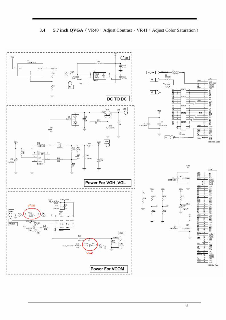
3.4
5.7 inch QVGA(VR40:Adjust Contrast,VR41:Adjust Color Saturation)
8
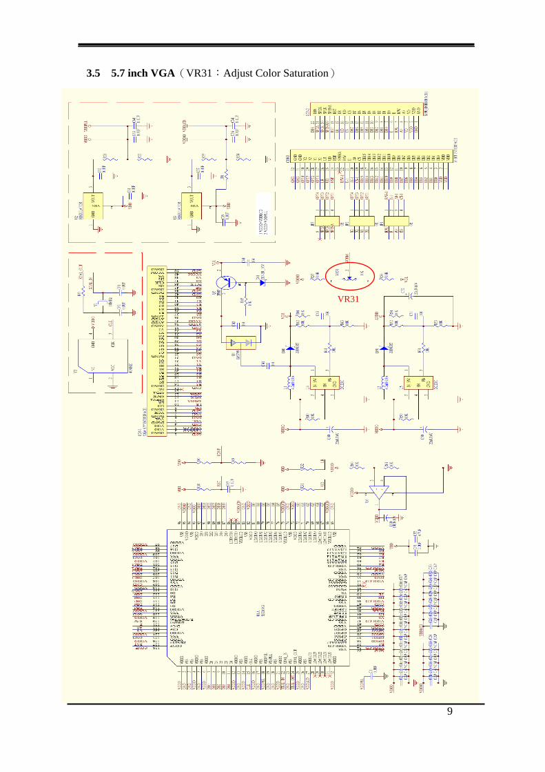
3.5 5.7 inch VGA(VR31:Adjust Color Saturation) 1
VR3
9
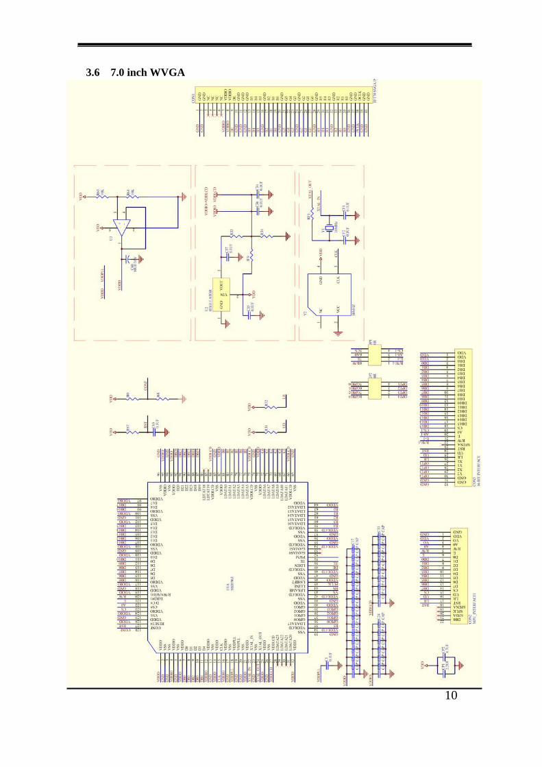
3.6 7.0 inch WVGA
10
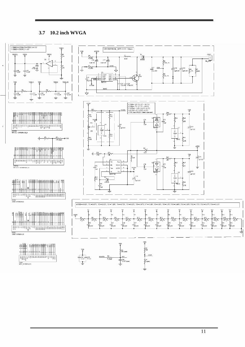
3.7 10.2 inch WVGA
11
4 MCU Interface Timing
4.1 Parallel 6800-series Interface Timing
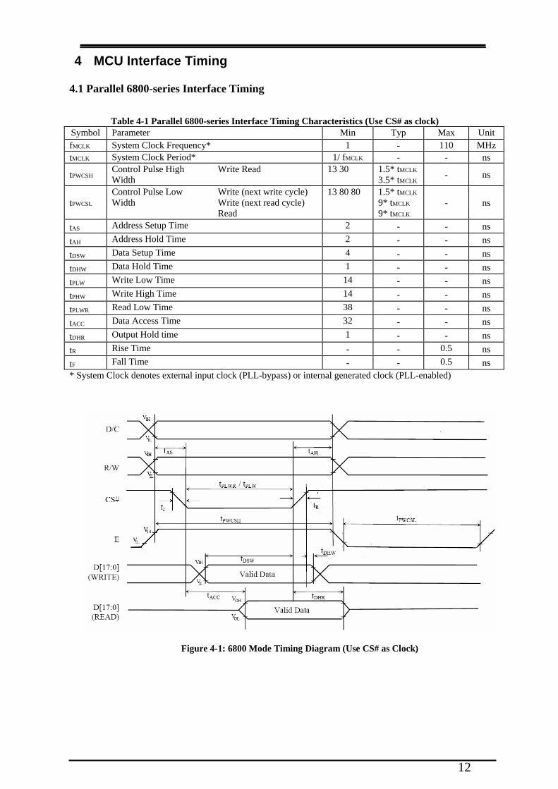
Table 4-1 Parallel 6800-series Interface Timing Characteristics (Use CS# as clock) Symbol Parameter Min Typ Max Unit fMCLK System Clock Frequency* 1 - 110 MHz tMCLK System Clock Period* 1/ fMCLK - - ns
tPWCSH Control Pulse High Width
Write Read 13 30 1.5* tMCLK
3.5* tMCLK - ns
tPWCSL
Control Pulse Low Width
Write (next write cycle) Write (next read cycle) Read
13 80 80 1.5* tMCLK
9* tMCLK
9* tMCLK
- ns
tAS Address Setup Time 2 - - ns tAH Address Hold Time 2 - - ns tDSW Data Setup Time 4 - - ns tDHW Data Hold Time 1 - - ns tPLW Write Low Time 14 - - ns tPHW Write High Time 14 - - ns tPLWR Read Low Time 38 - - ns tACC Data Access Time 32 - - ns tDHR Output Hold time 1 - - ns tR Rise Time - - 0.5 ns tF Fall Time - - 0.5 ns * System Clock denotes external input clock (PLL-bypass) or internal generated clock (PLL-enabled)
Figure 4-1: 6800 Mode Timing Diagram (Use CS# as Clock)
12
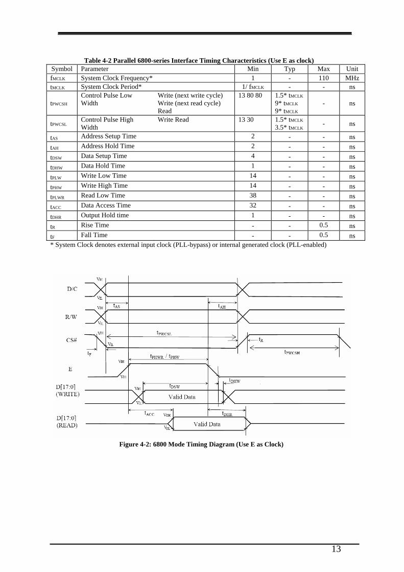
Table 4-2 Parallel 6800-series Interface Timing Characteristics (Use E as clock) Symbol Parameter Min Typ Max Unit fMCLK System Clock Frequency* 1 - 110 MHz tMCLK System Clock Period* 1/ fMCLK - - ns
tPWCSH
Control Pulse Low Width
Write (next write cycle) Write (next read cycle) Read
13 80 80 1.5* tMCLK
9* tMCLK
9* tMCLK
- ns
tPWCSL Control Pulse High Width
Write Read 13 30 1.5* tMCLK
3.5* tMCLK - ns
tAS Address Setup Time 2 - - ns tAH Address Hold Time 2 - - ns tDSW Data Setup Time 4 - - ns tDHW Data Hold Time 1 - - ns tPLW Write Low Time 14 - - ns tPHW Write High Time 14 - - ns tPLWR Read Low Time 38 - - ns tACC Data Access Time 32 - - ns tDHR Output Hold time 1 - - ns tR Rise Time - - 0.5 ns tF Fall Time - - 0.5 ns * System Clock denotes external input clock (PLL-bypass) or internal generated clock (PLL-enabled)
Figure 4-2: 6800 Mode Timing Diagram (Use E as Clock)
13
4.2 Parallel 8080-series Interface Timing
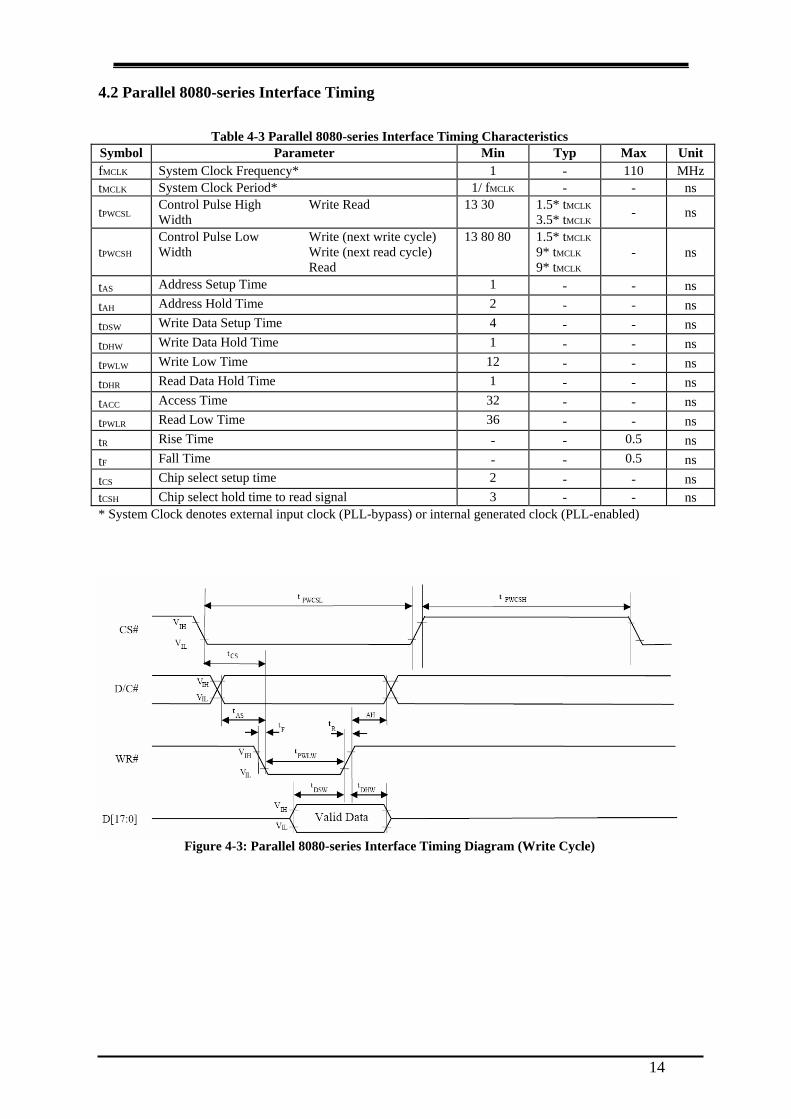
Table 4-3 Parallel 8080-series Interface Timing Characteristics
Symbol Parameter Min Typ Max Unit fMCLK System Clock Frequency* 1 - 110 MHz tMCLK System Clock Period* 1/ fMCLK - - ns
tPWCSL Control Pulse High Width
Write Read 13 30 1.5* tMCLK
3.5* tMCLK - ns
tPWCSH
Control Pulse Low Width
Write (next write cycle) Write (next read cycle) Read
13 80 80 1.5* tMCLK
9* tMCLK
9* tMCLK
- ns
tAS Address Setup Time 1 - - ns tAH Address Hold Time 2 - - ns tDSW Write Data Setup Time 4 - - ns tDHW Write Data Hold Time 1 - - ns tPWLW Write Low Time 12 - - ns tDHR Read Data Hold Time 1 - - ns tACC Access Time 32 - - ns tPWLR Read Low Time 36 - - ns tR Rise Time - - 0.5 ns tF Fall Time - - 0.5 ns tCS Chip select setup time 2 - - ns tCSH Chip select hold time to read signal 3 - - ns * System Clock denotes external input clock (PLL-bypass) or internal generated clock (PLL-enabled)
Figure 4-3: Parallel 8080-series Interface Timing Diagram (Write Cycle)
14
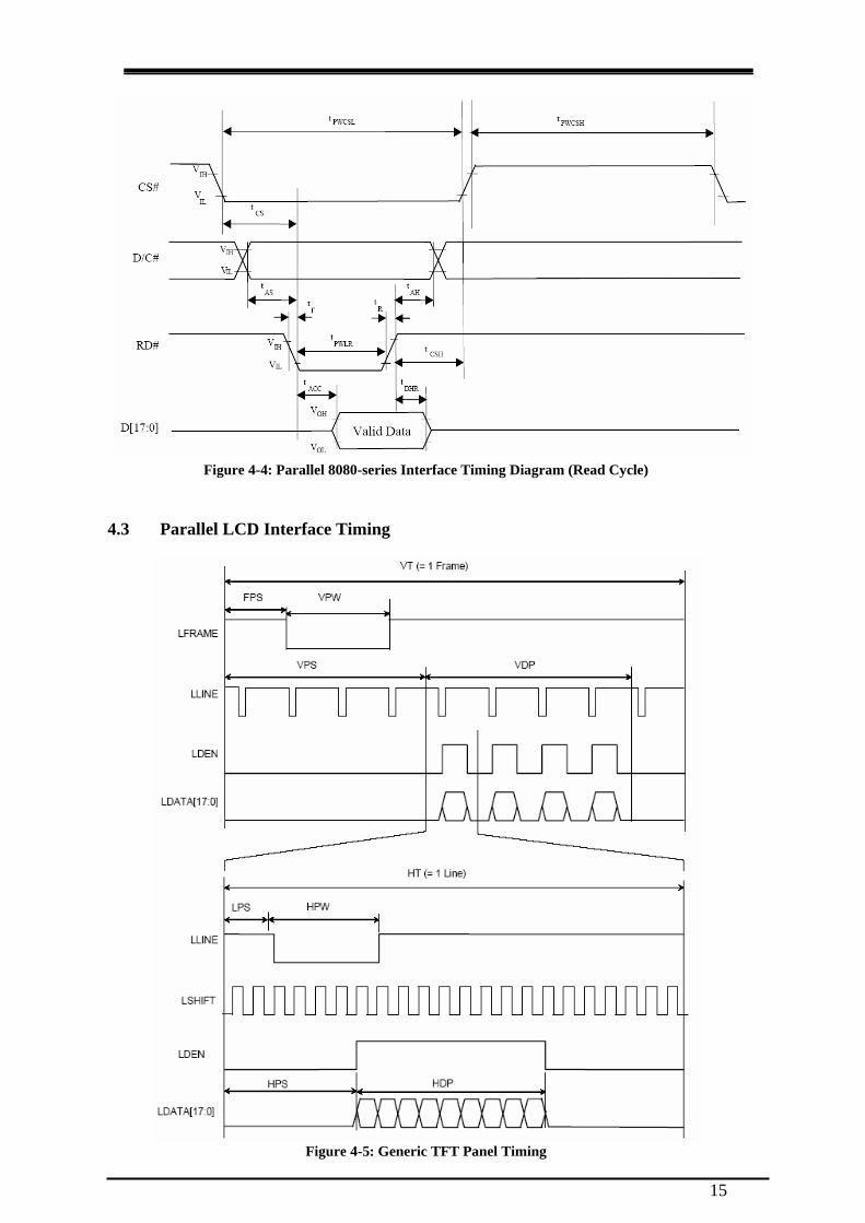
Figure 4-4: Parallel 8080-series Interface Timing Diagram (Read Cycle)
4.3 Parallel LCD Interface Timing
Figure 4-5: Generic TFT Panel Timing
15
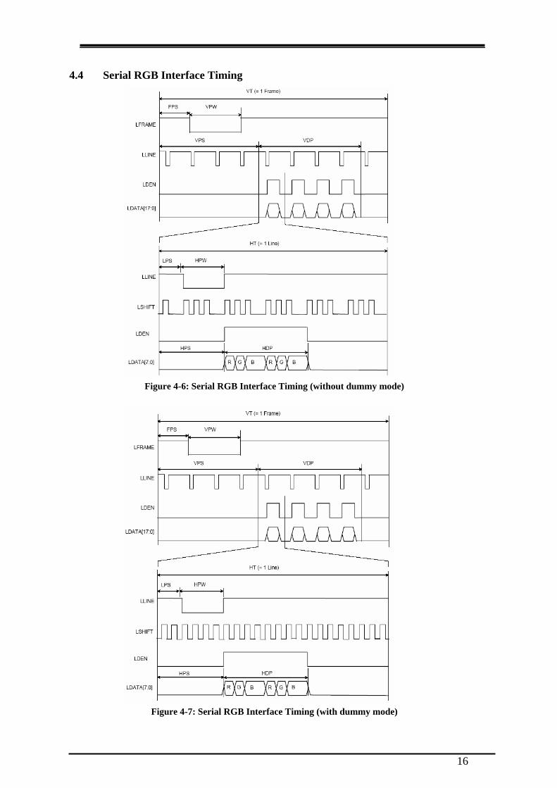
4.4 Serial RGB Interface Timing
Figure 4-6: Serial RGB Interface Timing (without dummy mode)
Figure 4-7: Serial RGB Interface Timing (with dummy mode)
16
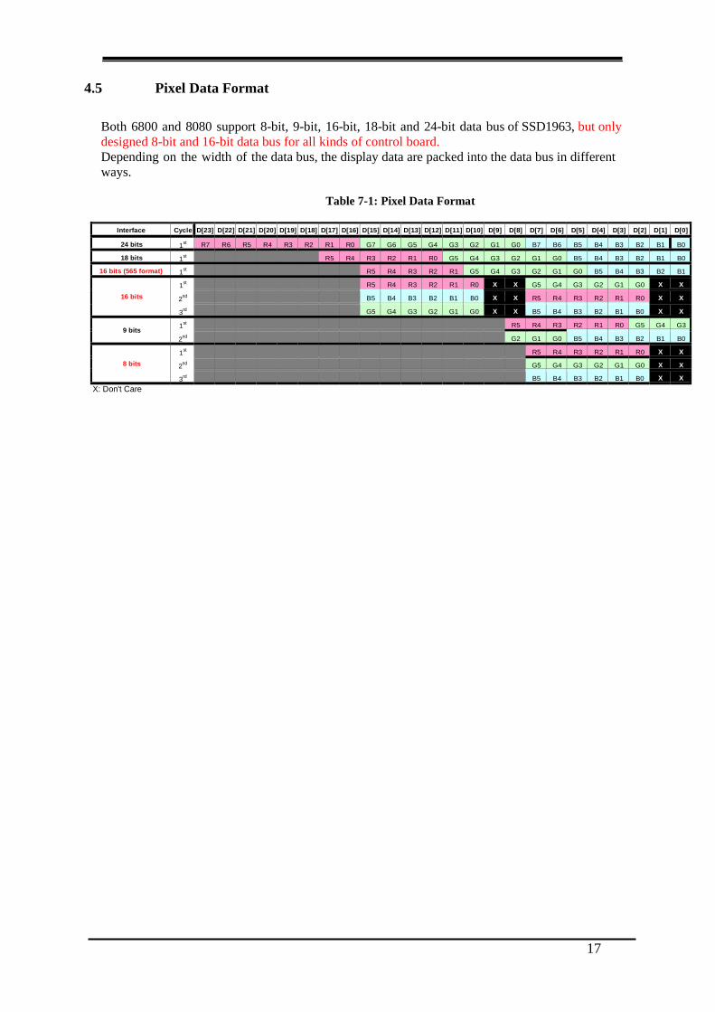
4.5 Pixel Data Format
Both 6800 and 8080 support 8-bit, 9-bit, 16-bit, 18-bit and 24-bit data bus of SSD1963, but only designed 8-bit and 16-bit data bus for all kinds of control board. Depending on the width of the data bus, the display data are packed into the data bus in different ways.
Table 7-1: Pixel Data Format
Interface Cycl e D[23] D[22] D[21] D[20] D[19] D[18] D[17] D[16] D[15] D[14] D[13] D[12] D[11] D[10] D[9] D[8] D[7] D[6] D[5] D[4] D[3] D[2] D[1] D[0]
24 bits 1st R7 R6 R5 R4 R3 R2 R1 R0 G7 G6 G5 G4 G3 G2 G1 G0 B7 B6 B5 B4 B3 B2 B1 B0
18 bits 1st R5 R4 R3 R2 R1 R0 G5 G4 G3 G2 G1 G0 B5 B4 B3 B2 B1 B0
16 bits (565 format) 1st R5 R4 R3 R2 R1 G5 G4 G3 G2 G1 G0 B5 B4 B3 B2 B1
R5 R4 R3 R2 R1 R0 X X G5 G4 G3 G2 G1 G0 X X
B5 B4 B3 B2 B1 B0 X X R5 R4 R3 R2 R1 R0 X X
16 bits 1st
2nd
3rd G5 G4 G3 G2 G1 G0 X X B5 B4 B3 B2 B1 B0 X X
R5 R4 R3 R2 R1 R0 G5 G4 G3 9 bits 1st
2nd G2 G1 G0 B5 B4 B3 B2 B1 B0
R5 R4 R3 R2 R1 R0 X X
G5 G4 G3 G2 G1 G0 X X
8 bits 1st
2nd
3rd B5 B4 B3 B2 B1 B0 X XX: Don't Care
17
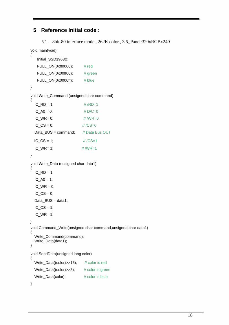
5 Reference Initial code :
5.1 8bit-80 interface mode , 262K color , 3.5_Panel:320xRGBx240
void main(void) {
Initial_SSD1963();
FULL_ON(0xff0000); // red
FULL_ON(0x00ff00); // green
FULL_ON(0x0000ff); // blue
} void Write_Command (unsigned char command) {
IC_RD = 1; // /RD=1
IC_A0 = 0; // D/C=0
IC_WR= 0; // /WR=0
IC_CS = 0; // /CS=0
Data_BUS = command; // Data Bus OUT
IC_CS = 1; // /CS=1
IC_WR= 1; // /WR=1
} void Write_Data (unsigned char data1) {
IC_RD = 1;
IC_A0 = 1;
IC_WR = 0;
IC_CS = 0;
Data_BUS = data1;
IC_CS = 1;
IC_WR= 1;
}
void Command_Write(unsigned char command,unsigned char data1) {
Write_Command(command); Write_Data(data1);
} void SendData(unsigned long color) {
Write_Data((color)>>16); // color is red
Write_Data((color)>>8); // color is green
Write_Data(color); // color is blue
} 18
void Initial_SSD1963 (void) //for 3.5 QVGA
{ IC_RST = 0; _nop_(); _nop_(); _nop_(); IC_RST = 1; _nop_(); _nop_(); _nop_(); Write_Command(0x01); //Software Reset
Write_Command(0x01);
Write_Command(0x01);
Command_Write(0xe0,0x01); // START PLL
Command_Write(0xe0,0x03); // LOCK PLL
Write_Command(0xb0); //SET LCD MODE SET TFT 18Bits MODE
Write_Data(0x0c); //SET TFT MODE & hsync+Vsync+DEN MODE
Write_Data(0x00); //SET TFT MODE & hsync+Vsync+DEN MODE
Write_Data(0x01); //SET horizontal size=320-1 HightByte
Write_Data(0x3f); //SET horizontal size=320-1 LowByte
Write_Data(0x00); //SET vertical size=240-1 HightByte
Write_Data(0xef); //SET vertical size=240-1 LowByte
Write_Data(0x00); //SET even/odd line RGB seq.=RGB
Command_Write(0xf0,0x00); //SET pixel data I/F format=8bit
Command_Write(0x3a,0x60); // SET R G B format = 6 6 6
Write_Command(0xe2); //SET PLL freq=113.33MHz ;
Write_Data(0x22);
Write_Data(0x03);
Write_Data(0x04);
Write_Command(0xe6); //SET PCLK freq=6.5MHz/19MHz ; pixel clock frequency
Write_Data(0x00); //0x02
Write_Data(0xea); //0xb0
Write_Data(0xec); //0xb5
Write_Command(0xb4); //SET HBP
Write_Data(0x01); //SET HSYNC Total = 440
Write_Data(0xb8);
Write_Data(0x00); //SET HBP = 68
Write_Data(0x44);
19

Write_Data(0x0f); //SET VBP 16 = 15 + 1
Write_Data(0x00); //SET Hsync pulse start position
Write_Data(0x00);
Write_Data(0x00); //SET Hsync pulse subpixel start position
Write_Command(0xb6); //SET VBP
Write_Data(0x01); //SET Vsync total 265 = 264 + 1
Write_Data(0x08);
Write_Data(0x00); //SET VBP = 18
Write_Data(0x12);
Write_Data(0x07); //SET Vsync pulse 8 = 7 + 1
Write_Data(0x00); //SET Vsync pulse start position
Write_Data(0x00);
Write_Command(0x2a); //SET column address
Write_Data(0x00); //SET start column address=0
Write_Data(0x00);
Write_Data(0x01); //SET end column address=320
Write_Data(0x3f);
Write_Command(0x2b); //SET page address
Write_Data(0x00); //SET start page address=0
Write_Data(0x00);
Write_Data(0x00); //SET end page address=240
Write_Data(0xef);
Write_Command(0x29); //SET display on
Write_Command(0x2c);
}
20
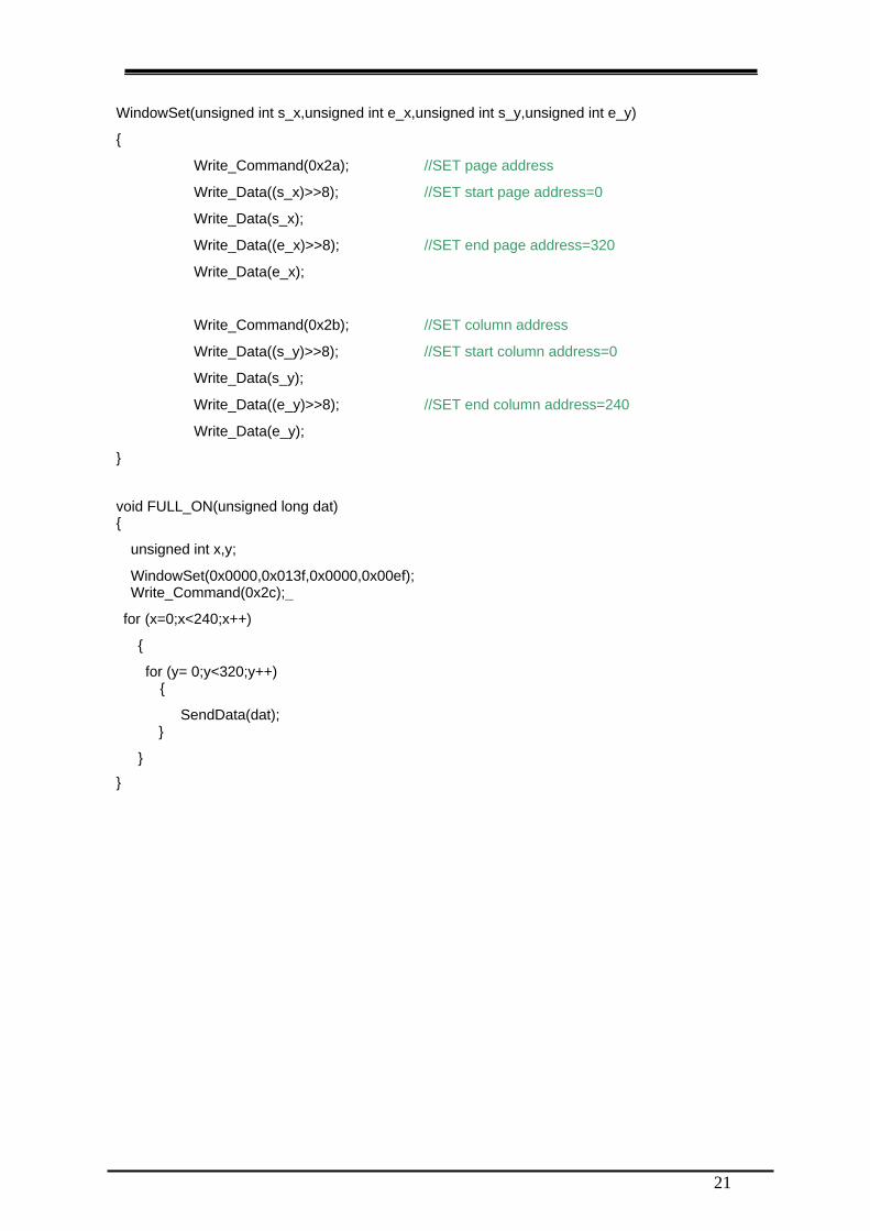
WindowSet(unsigned int s_x,unsigned int e_x,unsigned int s_y,unsigned int e_y)
{
Write_Command(0x2a); //SET page address
Write_Data((s_x)>>8); //SET start page address=0
Write_Data(s_x);
Write_Data((e_x)>>8); //SET end page address=320
Write_Data(e_x);
Write_Command(0x2b); //SET column address
Write_Data((s_y)>>8); //SET start column address=0
Write_Data(s_y);
Write_Data((e_y)>>8); //SET end column address=240
Write_Data(e_y);
} void FULL_ON(unsigned long dat) {
unsigned int x,y;
WindowSet(0x0000,0x013f,0x0000,0x00ef); Write_Command(0x2c);_
for (x=0;x<240;x++)
{
for (y= 0;y<320;y++) {
SendData(dat); }
} }
21
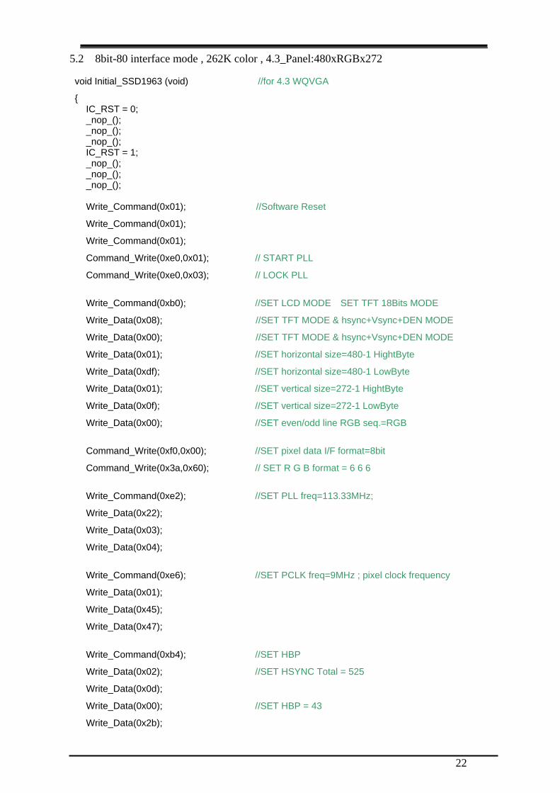
5.2 8bit-80 interface mode , 262K color , 4.3_Panel:480xRGBx272 void Initial_SSD1963 (void) //for 4.3 WQVGA
{ IC_RST = 0; _nop_(); _nop_(); _nop_(); IC_RST = 1; _nop_(); _nop_(); _nop_(); Write_Command(0x01); //Software Reset
Write_Command(0x01);
Write_Command(0x01);
Command_Write(0xe0,0x01); // START PLL
Command_Write(0xe0,0x03); // LOCK PLL
Write_Command(0xb0); //SET LCD MODE SET TFT 18Bits MODE
Write_Data(0x08); //SET TFT MODE & hsync+Vsync+DEN MODE
Write_Data(0x00); //SET TFT MODE & hsync+Vsync+DEN MODE
Write_Data(0x01); //SET horizontal size=480-1 HightByte
Write_Data(0xdf); //SET horizontal size=480-1 LowByte
Write_Data(0x01); //SET vertical size=272-1 HightByte
Write_Data(0x0f); //SET vertical size=272-1 LowByte
Write_Data(0x00); //SET even/odd line RGB seq.=RGB
Command_Write(0xf0,0x00); //SET pixel data I/F format=8bit
Command_Write(0x3a,0x60); // SET R G B format = 6 6 6
Write_Command(0xe2); //SET PLL freq=113.33MHz;
Write_Data(0x22);
Write_Data(0x03);
Write_Data(0x04);
Write_Command(0xe6); //SET PCLK freq=9MHz ; pixel clock frequency
Write_Data(0x01);
Write_Data(0x45);
Write_Data(0x47);
Write_Command(0xb4); //SET HBP
Write_Data(0x02); //SET HSYNC Total = 525
Write_Data(0x0d);
Write_Data(0x00); //SET HBP = 43
Write_Data(0x2b);
22
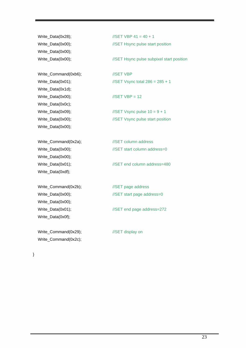
Write_Data(0x28); //SET VBP 41 = 40 + 1
Write_Data(0x00); //SET Hsync pulse start position
Write_Data(0x00);
Write_Data(0x00); //SET Hsync pulse subpixel start position
Write_Command(0xb6); //SET VBP
Write_Data(0x01); //SET Vsync total 286 = 285 + 1
Write_Data(0x1d);
Write_Data(0x00); //SET VBP = 12
Write_Data(0x0c);
Write_Data(0x09); //SET Vsync pulse 10 = 9 + 1
Write_Data(0x00); //SET Vsync pulse start position
Write_Data(0x00);
Write_Command(0x2a); //SET column address
Write_Data(0x00); //SET start column address=0
Write_Data(0x00);
Write_Data(0x01); //SET end column address=480
Write_Data(0xdf);
Write_Command(0x2b); //SET page address
Write_Data(0x00); //SET start page address=0
Write_Data(0x00);
Write_Data(0x01); //SET end page address=272
Write_Data(0x0f);
Write_Command(0x29); //SET display on
Write_Command(0x2c);
}
23
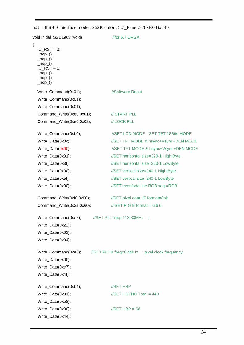
5.3 8bit-80 interface mode , 262K color , 5.7_Panel:320xRGBx240 void Initial_SSD1963 (void) //for 5.7 QVGA
{ IC_RST = 0; _nop_(); _nop_(); _nop_(); IC_RST = 1; _nop_(); _nop_(); _nop_(); Write_Command(0x01); //Software Reset
Write_Command(0x01);
Write_Command(0x01);
Command_Write(0xe0,0x01); // START PLL
Command_Write(0xe0,0x03); // LOCK PLL
Write_Command(0xb0); //SET LCD MODE SET TFT 18Bits MODE
Write_Data(0x0c); //SET TFT MODE & hsync+Vsync+DEN MODE
Write_Data(0x00); //SET TFT MODE & hsync+Vsync+DEN MODE
Write_Data(0x01); //SET horizontal size=320-1 HightByte
Write_Data(0x3f); //SET horizontal size=320-1 LowByte
Write_Data(0x00); //SET vertical size=240-1 HightByte
Write_Data(0xef); //SET vertical size=240-1 LowByte
Write_Data(0x00); //SET even/odd line RGB seq.=RGB
Command_Write(0xf0,0x00); //SET pixel data I/F format=8bit
Command_Write(0x3a,0x60); // SET R G B format = 6 6 6
Write_Command(0xe2); //SET PLL freq=113.33MHz ;
Write_Data(0x22);
Write_Data(0x03);
Write_Data(0x04);
Write_Command(0xe6); //SET PCLK freq=6.4MHz ; pixel clock frequency
Write_Data(0x00);
Write_Data(0xe7);
Write_Data(0x4f);
Write_Command(0xb4); //SET HBP
Write_Data(0x01); //SET HSYNC Total = 440
Write_Data(0xb8);
Write_Data(0x00); //SET HBP = 68
Write_Data(0x44);
24
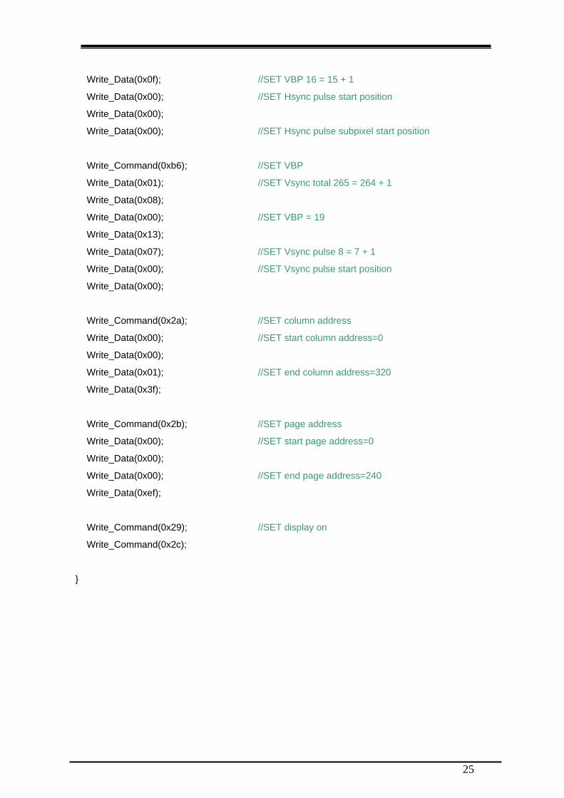
Write_Data(0x0f); //SET VBP 16 = 15 + 1
Write_Data(0x00); //SET Hsync pulse start position
Write_Data(0x00);
Write_Data(0x00); //SET Hsync pulse subpixel start position
Write_Command(0xb6); //SET VBP
Write_Data(0x01); //SET Vsync total 265 = 264 + 1
Write_Data(0x08);
Write_Data(0x00); //SET VBP = 19
Write_Data(0x13);
Write_Data(0x07); //SET Vsync pulse 8 = 7 + 1
Write_Data(0x00); //SET Vsync pulse start position
Write_Data(0x00);
Write_Command(0x2a); //SET column address
Write_Data(0x00); //SET start column address=0
Write_Data(0x00);
Write_Data(0x01); //SET end column address=320
Write_Data(0x3f);
Write_Command(0x2b); //SET page address
Write_Data(0x00); //SET start page address=0
Write_Data(0x00);
Write_Data(0x00); //SET end page address=240
Write_Data(0xef);
Write_Command(0x29); //SET display on
Write_Command(0x2c);
}
25
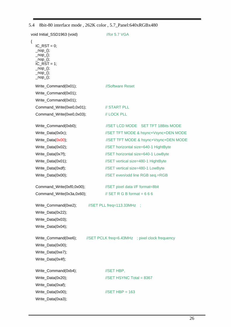
5.4 8bit-80 interface mode , 262K color , 5.7_Panel:640xRGBx480 void Initial_SSD1963 (void) //for 5.7 VGA
{ IC_RST = 0; _nop_(); _nop_(); _nop_(); IC_RST = 1; _nop_(); _nop_(); _nop_(); Write_Command(0x01); //Software Reset
Write_Command(0x01);
Write_Command(0x01);
Command_Write(0xe0,0x01); // START PLL
Command_Write(0xe0,0x03); // LOCK PLL
Write_Command(0xb0); //SET LCD MODE SET TFT 18Bits MODE
Write_Data(0x0c); //SET TFT MODE & hsync+Vsync+DEN MODE
Write_Data(0x00); //SET TFT MODE & hsync+Vsync+DEN MODE
Write_Data(0x02); //SET horizontal size=640-1 HightByte
Write_Data(0x7f); //SET horizontal size=640-1 LowByte
Write_Data(0x01); //SET vertical size=480-1 HightByte
Write_Data(0xdf); //SET vertical size=480-1 LowByte
Write_Data(0x00); //SET even/odd line RGB seq.=RGB
Command_Write(0xf0,0x00); //SET pixel data I/F format=8bit
Command_Write(0x3a,0x60); // SET R G B format = 6 6 6
Write_Command(0xe2); //SET PLL freq=113.33MHz ;
Write_Data(0x22);
Write_Data(0x03);
Write_Data(0x04);
Write_Command(0xe6); //SET PCLK freq=6.43MHz ; pixel clock frequency
Write_Data(0x00);
Write_Data(0xe7);
Write_Data(0x4f);
Write_Command(0xb4); //SET HBP,
Write_Data(0x20); //SET HSYNC Total = 8367
Write_Data(0xaf);
Write_Data(0x00); //SET HBP = 163
Write_Data(0xa3);
26
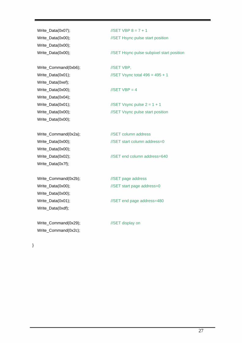
Write_Data(0x07); //SET VBP 8 = 7 + 1
Write_Data(0x00); //SET Hsync pulse start position
Write_Data(0x00);
Write_Data(0x00); //SET Hsync pulse subpixel start position
Write_Command(0xb6); //SET VBP,
Write_Data(0x01); //SET Vsync total 496 = 495 + 1
Write_Data(0xef);
Write_Data(0x00); //SET VBP = 4
Write_Data(0x04);
Write_Data(0x01); //SET Vsync pulse 2 = 1 + 1
Write_Data(0x00); //SET Vsync pulse start position
Write_Data(0x00);
Write_Command(0x2a); //SET column address
Write_Data(0x00); //SET start column address=0
Write_Data(0x00);
Write_Data(0x02); //SET end column address=640
Write_Data(0x7f);
Write_Command(0x2b); //SET page address
Write_Data(0x00); //SET start page address=0
Write_Data(0x00);
Write_Data(0x01); //SET end page address=480
Write_Data(0xdf);
Write_Command(0x29); //SET display on
Write_Command(0x2c);
}
27

5.5 8bit-80 interface mode , 262K color , 7.0_Panel:800xRGBx480 void Initial_SSD1963 (void) //for 7.0 VGA
{ IC_RST = 0; _nop_(); _nop_(); _nop_(); IC_RST = 1; _nop_(); _nop_(); _nop_(); Write_Command(0x01); //Software Reset
Write_Command(0x01);
Write_Command(0x01);
Command_Write(0xe0,0x01); // START PLL
Command_Write(0xe0,0x03); // LOCK PLL
Write_Command(0xb0); //SET LCD MODE SET TFT 18Bits MODE
Write_Data(0x08); //SET TFT MODE & hsync+Vsync+DEN MODE
Write_Data(0x00); //SET TFT MODE & hsync+Vsync+DEN MODE
Write_Data(0x03); //SET horizontal size=800-1 HightByte
Write_Data(0x1f); //SET horizontal size=800-1 LowByte
Write_Data(0x01); //SET vertical size=480-1 HightByte
Write_Data(0xdf); //SET vertical size=480-1 LowByte
Write_Data(0x00); //SET even/odd line RGB seq.=RGB
Command_Write(0xf0,0x00); //SET pixel data I/F format=8bit
Command_Write(0x3a,0x60); // SET R G B format = 6 6 6
Write_Command(0xe2); //SET PLL freq=113.33MHz ;
Write_Data(0x22);
Write_Data(0x03);
Write_Data(0x04);
Write_Command(0xe6); //SET PCLK freq=33.26MHz ; pixel clock frequency
Write_Data(0x00);
Write_Data(0xe7);
Write_Data(0x4f);
Write_Command(0xb4); //SET HBP,
Write_Data(0x20); //SET HSYNC Total = 8367
Write_Data(0xaf);
Write_Data(0x00); //SET HBP = 163
Write_Data(0xa3);
28
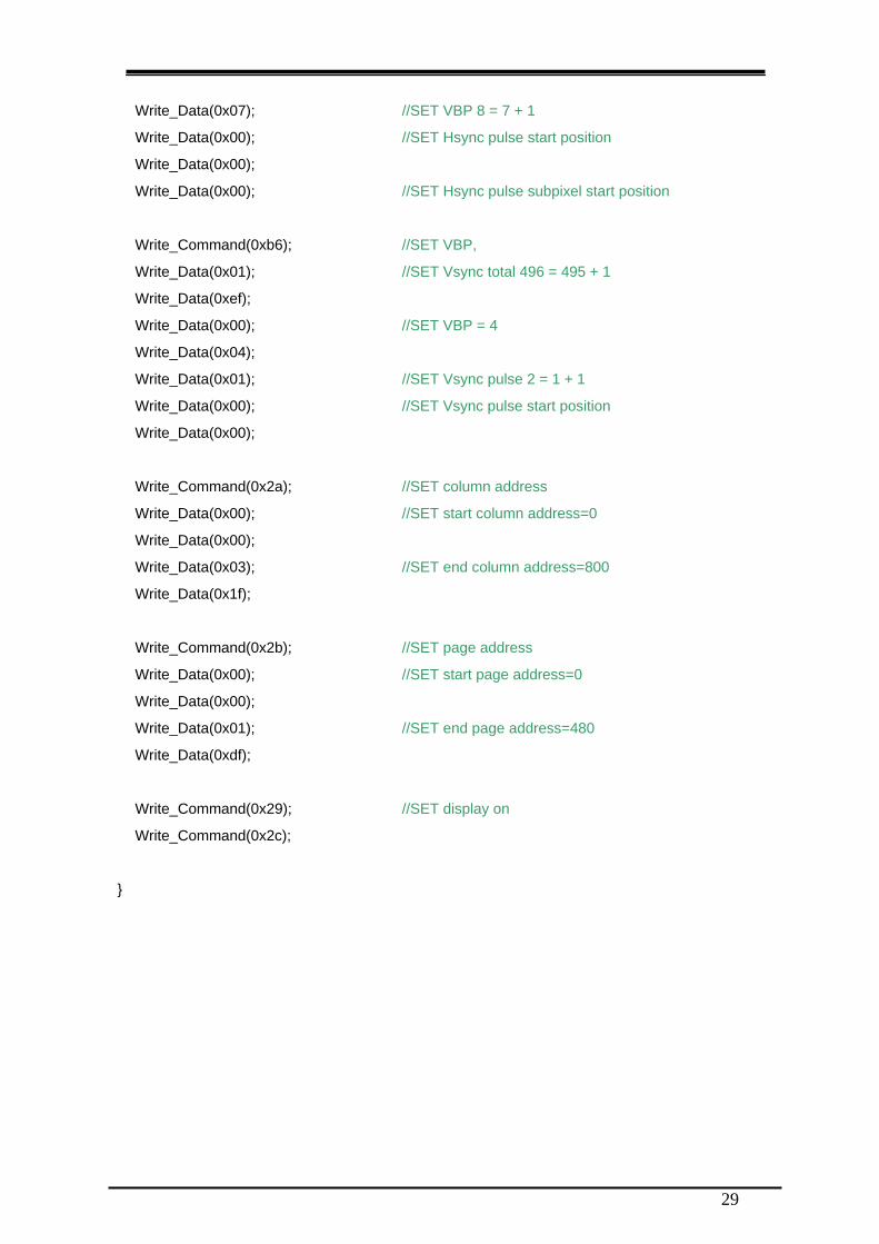
Write_Data(0x07); //SET VBP 8 = 7 + 1
Write_Data(0x00); //SET Hsync pulse start position
Write_Data(0x00);
Write_Data(0x00); //SET Hsync pulse subpixel start position
Write_Command(0xb6); //SET VBP,
Write_Data(0x01); //SET Vsync total 496 = 495 + 1
Write_Data(0xef);
Write_Data(0x00); //SET VBP = 4
Write_Data(0x04);
Write_Data(0x01); //SET Vsync pulse 2 = 1 + 1
Write_Data(0x00); //SET Vsync pulse start position
Write_Data(0x00);
Write_Command(0x2a); //SET column address
Write_Data(0x00); //SET start column address=0
Write_Data(0x00);
Write_Data(0x03); //SET end column address=800
Write_Data(0x1f);
Write_Command(0x2b); //SET page address
Write_Data(0x00); //SET start page address=0
Write_Data(0x00);
Write_Data(0x01); //SET end page address=480
Write_Data(0xdf);
Write_Command(0x29); //SET display on
Write_Command(0x2c);
}
29
5.6 8bit-80 interface mode , 262K color , 10.2_Panel:800xRGBx480 void Initial_SSD1963 (void) {
IC_RST = 0; _nop_(); _nop_(); _nop_(); IC_RST = 1; _nop_(); _nop_(); _nop_();
Write_Command(0x01); //Software Reset
Write_Command(0x01);
Write_Command(0x01);
Command_Write(0xe0,0x01); //START PLL
Command_Write(0xe0,0x03); //LOCK PLL
Write_Command(0xb0); //SET LCD panel mode and resolution
Write_Data(0x08); //TFT FRC enable, 18-bit data
Write_Data(0x00); //TFT mode
Write_Data(0x03); //SET horizontal size=800-1 HightByte
Write_Data(0x1f); //SET horizontal size=800-1 LowByte
Write_Data(0x01); //SET vertical size=480-1 HightByte
Write_Data(0xdf); //SET vertical size=480-1 LowByte
Write_Data(0x2d); //SET even/odd line RGB seq.=RGB
Command_Write(0xf0,0x00); //SET pixel data I/F format=8bit
Command_Write(0x36,0x00); //SET read from frame buffer to the display is RGB
Write_Command(0xe2); //SET PLL freq=87.5MHz //沿用之前的尺寸的設定
Write_Data(0x22); //34
Write_Data(0x03); // 3
Write_Data(0x04);
Write_Command(0xe6); //SET PCLK freq=40MHz ; pixel clock frequency
Write_Data(0x74);
Write_Data(0x50);
Write_Data(0x07);
Write_Command(0xb4); //SET Horizontal period
Write_Data(0x04); //SET HT+1 = 1061 pixels (higher byte)
Write_Data(0x25); //lower byte
Write_Data(0x00); //SET Horizontal sync pulse start position = HPS = 52 pixels
30
Write_Data(0x34); //lower byte
Write_Data(0x05); //SET (HPW+1) pixels => 5 = 4 + 1 pixels
Write_Data(0x00); //SET LPS pixels (higher byte)
Write_Data(0x00); //lower byte
Write_Data(0x00); //SET Hsync pulse subpixel start position for serial TFT interface
Write_Command(0xb6); //SET Vertical period
Write_Data(0x02); //SET (VT+1) lines =>530 = 529 + 1 lines (higher byte)
Write_Data(0x12); //lower byte
Write_Data(0x00); //SET VPS lines = 29 lines (higher byte)
Write_Data(0x1d); //lower byte
Write_Data(0x05); //SET (VPW+1) lines => 5 = 4 + 1 lines
Write_Data(0x00); //SET FPS lines (higher byte)
Write_Data(0x00); //lower byte
Write_Command(0x2a); //SET column address
Write_Data(0x00); //SET start column address=0
Write_Data(0x00);
Write_Data(0x03); //SET end column address=799
Write_Data(0x1f);
Write_Command(0x2b); //SET page address
Write_Data(0x00); //SET start page address=0
Write_Data(0x00);
Write_Data(0x01); //SET end page address=479
Write_Data(0xdf);
//Write_Command(0x21);
Write_Command(0x29); //SET display on
Write_Command(0x2c); //write memory start
} 31


![TFT-DISPLAYS - endrich.com · endrich components o lie tft-displays – automotive grÖsse disp auflÖsung helligkeit tikelbezeichnung backlight lebensdauer [cd/m²] schnittstelle](https://img.pdfslide.org/doc/110x75/5b1483247f8b9a257c8d73d0/tft-displays-endrich-components-o-lie-tft-displays-automotive-groesse.jpg)