Embed Size (px)
Citation preview
Masterarbeit
Design and Implementation of a Self-test
Concept for an Industrial Multi-core
Microcontroller
Burim ALIU
————————————–
Institut fur Technische Informatik
Technische Universitat Graz
Begutachter: Ass.-Prof. Dipl.-Ing.Dr. techn.Christian Steger
Betreuer: Ass.-Prof. Dipl.-Ing.Dr. techn.Christian Steger
Dipl.-Ing.Roland Mader
Graz, im Mai 2012
Kurzfassung
Seit einigen Jahren werden Mikrocontroller in der Automobilindustrie als Steuergeratefur Bremsen oder Motorsteuerungen genutzt. Heutzutage gibt es viele Multi-Core Mikro-controller, die aber nicht alle fur sicherheitskritische Anwendungen in der Automobilin-dustrie verwendet werden konnen.
Immer, wenn einige kritische Aufgaben ausgefuhrt werden mussen, muss sichergestelltsein, dass der Mikrocontroller ordnungsgemaß funktioniert und das die funktionale Sicher-heit im System erhalten bleibt.
Wahrend der Laufzeit konnen Storungen (z.B. Ubergangsfehler, gekoppelte Fehlerusw.) in den verschiedenen Teilen des Mikrocontrollers auftreten. Diese Fehler konnen zuAusfallen des gesamten Systems fuhren.
Zur Erkennung und Handhabung solcher Fehler sind Mikrocontroller mit diversenSicherheitsfunktionalitaten ausgestattet. Diese konnen in Form von Architekturen einesLock-Step Modus, asymmetrischen Modus, symmetrischen Modus oder Selbsttests real-isiert sein, die entweder in Hardware oder in Software implementiert werden.
In dieser Arbeit wurden verschiedene Multi-Core-Architekturen und verschiedene Selb-sttestalgorithmen bewertet.
Das erste Ziel war, zur Verfugung stehende Multi-Core-Mikrocontroller mit Bezugauf die gewahlten Kriterien zu bewerten. Ein weiteres Ziel war die Entwicklung undImplementierung eines Online-Selbsttest-Konzepts fur einen ausgewahlten Multi-Core-Mikrocontroller. Dieses Konzept beinhaltet, software- und hardwarebasierte Selbsttestsfur bestimmte Teile des ausgewahlten Mikrocontrollers wie RAM oder CPU.
Diese Hardware und softwarebasierten Selbsttests werden durch einen externen Watch-dog erganzt, der es ermoglicht, den Programmablauf zu uberwachen.
1
Abstract
During the last years microcontrollers have been used for control devices in the auto-motive industry like auto-brakes, motor control etc. Nowadays there are many multi-coremicrocontrollers, but not all of them can be used in the automotive industry for safetycritical applications. Whenever some critical tasks are executed, it must be ensured thatthe microcontroller is working correctly and the system maintains the functional safety.
During runtime, faults can occur in various parts of the microcontroller such as ALU,RAM or peripherals starting from, stuck at faults, transition faults, coupled faults etc.These faults can cause failures of the complete system.
To detect and handle such faults, microcontrollers are equipped with safety features inthe form of architectures like lock-step mode, asymmetric mode, symmetric mode or selftests which are implemented either in hardware or in software.
Different multicore architectures and different self testing algorithms were reviewed forthe thesis. The first goal was to evaluate available multicore microcontrollers with respectto chosen evaluation criteria. Another goal was to design and implement an online selftest concept for a selected multi-core controller, which includes software based self testsas well as hardware built-in self tests for specific parts of the chosen microcontroller likeRAM or CPU cores. These hardware and software-based self tests are supplemented byan external watchdog that is used for the program flow monitoring.
2
STATUTORY DECLARATION
I declare that I have authored this thesis independently, that I have not used other thanthe declared sources / resources, and that I have explicitly marked all material which hasbeen quoted either literally or by content from the used sources.
.............................. ...........................................date (signature)
3
Acknowledgments
This thesis was performed at the Institute for Technical Informatics at the TechnicalUniversity of Graz in the scope of the MEPAS1 project in cooperation with AVL ListGmbH2 and The Virtual Vehicle Competence Center3.
First of all I want to thank my supervisors Dipl.-Ing. Roland Mader and Ass.-Prof.Dipl.-Ing. Dr. techn. Christian Steger who have supported me during the time I was workingon my thesis.
During my study I was greatly supported by my family: my father, my mother, andmy two brothers.
Graz, May 2012 Burim Aliu
1Methods and processes for automotive embedded software development, verification and validation2http://www.avl.com3http://www.vif.tugraz.at
4
Contents
1 Introduction 101.1 Motivation . . . . . . . . . . . . . . . . . . . . . . . . . . . . . . . . . . . . 101.2 Objective . . . . . . . . . . . . . . . . . . . . . . . . . . . . . . . . . . . . . 121.3 Structure . . . . . . . . . . . . . . . . . . . . . . . . . . . . . . . . . . . . . 12
2 Related Work 142.1 Hardware architectures and strategies . . . . . . . . . . . . . . . . . . . . . 14
2.1.1 Faults and Failures . . . . . . . . . . . . . . . . . . . . . . . . . . . . 142.1.2 Fail-Safe System Strategies . . . . . . . . . . . . . . . . . . . . . . . 16
2.1.2.1 Single Controller Strategy . . . . . . . . . . . . . . . . . . . 172.1.2.2 Symmetric Controller Strategy . . . . . . . . . . . . . . . . 172.1.2.3 Dual Core Controller Strategy . . . . . . . . . . . . . . . . 182.1.2.4 Asymmetric Controller Strategy . . . . . . . . . . . . . . . 192.1.2.5 Distributed Controller Strategy . . . . . . . . . . . . . . . . 19
2.1.3 Multi-core Architectures with redundant structures . . . . . . . . . . 202.1.3.1 Lock-Step Dual & Dual Lock-Step Processor Architectures 202.1.3.2 Loosely-Synchronized Dual & Triple Modular Processor
Architectures . . . . . . . . . . . . . . . . . . . . . . . . . . 212.1.3.3 Generic Dual Core Architecture . . . . . . . . . . . . . . . 21
2.2 Software strategies . . . . . . . . . . . . . . . . . . . . . . . . . . . . . . . . 232.2.1 Software Based Self tests . . . . . . . . . . . . . . . . . . . . . . . . 232.2.2 Functional Tests . . . . . . . . . . . . . . . . . . . . . . . . . . . . . 25
2.2.2.1 Software Fail-Safe Techniques . . . . . . . . . . . . . . . . . 272.2.2.2 March Tests . . . . . . . . . . . . . . . . . . . . . . . . . . 282.2.2.3 Abraham Test . . . . . . . . . . . . . . . . . . . . . . . . . 302.2.2.4 Galloping and Walking patterns . . . . . . . . . . . . . . . 322.2.2.5 Checkerboard . . . . . . . . . . . . . . . . . . . . . . . . . . 332.2.2.6 Butterfly Algorithm . . . . . . . . . . . . . . . . . . . . . . 34
2.2.3 Structural Tests . . . . . . . . . . . . . . . . . . . . . . . . . . . . . 342.2.4 On-line Periodic Tests . . . . . . . . . . . . . . . . . . . . . . . . . . 372.2.5 Specialized Tests for Multi-cores . . . . . . . . . . . . . . . . . . . . 39
3 Analysis and Design 423.1 Evaluated Architectures . . . . . . . . . . . . . . . . . . . . . . . . . . . . . 42
3.1.1 TMS570 - Texas Instruments . . . . . . . . . . . . . . . . . . . . . . 42
5
3.1.2 TC1766 - Infineon Technologies . . . . . . . . . . . . . . . . . . . . . 453.1.3 fRMethodology - Yogitech & Toshiba . . . . . . . . . . . . . . . . . 463.1.4 Evaluation Criteria . . . . . . . . . . . . . . . . . . . . . . . . . . . . 50
3.2 CPU, RAM and Peripheral tests in the TMS570 microcontroller . . . . . . 523.2.1 CPU Tests . . . . . . . . . . . . . . . . . . . . . . . . . . . . . . . . 523.2.2 Core Compare Module Tests . . . . . . . . . . . . . . . . . . . . . . 533.2.3 RAM and Peripheral Tests . . . . . . . . . . . . . . . . . . . . . . . 543.2.4 Error Signaling Module - ESM . . . . . . . . . . . . . . . . . . . . . 55
3.3 Functional Safety Requirements . . . . . . . . . . . . . . . . . . . . . . . . . 553.4 Design Concept . . . . . . . . . . . . . . . . . . . . . . . . . . . . . . . . . . 56
3.4.1 Modules . . . . . . . . . . . . . . . . . . . . . . . . . . . . . . . . . . 583.4.2 Properties of the modules . . . . . . . . . . . . . . . . . . . . . . . . 59
4 Implementation and Results 624.1 TMS570 Evaluation Board . . . . . . . . . . . . . . . . . . . . . . . . . . . . 624.2 Workflow and Tool Chain . . . . . . . . . . . . . . . . . . . . . . . . . . . . 654.3 Start-up Phase . . . . . . . . . . . . . . . . . . . . . . . . . . . . . . . . . . 674.4 Periodic Operation . . . . . . . . . . . . . . . . . . . . . . . . . . . . . . . . 69
4.4.1 RAM test . . . . . . . . . . . . . . . . . . . . . . . . . . . . . . . . . 694.4.2 Watchdog test . . . . . . . . . . . . . . . . . . . . . . . . . . . . . . 734.4.3 CPU test . . . . . . . . . . . . . . . . . . . . . . . . . . . . . . . . . 74
4.5 Fault Injection, Test Cases and Timing Results . . . . . . . . . . . . . . . . 75
5 Conclusions and Outlook 795.1 Conclusions . . . . . . . . . . . . . . . . . . . . . . . . . . . . . . . . . . . . 795.2 Outlook . . . . . . . . . . . . . . . . . . . . . . . . . . . . . . . . . . . . . . 80
A Definitions 81A.1 Abbreviations . . . . . . . . . . . . . . . . . . . . . . . . . . . . . . . . . . . 81A.2 Used Symbols . . . . . . . . . . . . . . . . . . . . . . . . . . . . . . . . . . . 83
Bibliography 84
6
List of Figures
1.1 Action chain for fault handling [Mon99] . . . . . . . . . . . . . . . . . . . . 11
2.1 Finite State Machines describing basic faults . . . . . . . . . . . . . . . . . 142.2 Single controller strategy [SD06] . . . . . . . . . . . . . . . . . . . . . . . . 172.3 Symmetric controller strategy [SD06] . . . . . . . . . . . . . . . . . . . . . . 182.4 Dual-Core controller strategy [SD06] . . . . . . . . . . . . . . . . . . . . . . 182.5 Asymmetric controller strategy [SD06] . . . . . . . . . . . . . . . . . . . . . 192.6 Distributed controller strategy [SD06] . . . . . . . . . . . . . . . . . . . . . 202.7 Architectures based on the Lock Step [BFM+03] . . . . . . . . . . . . . . . 212.8 TMR and Loosely-Synchronized Dual Architecture [BFM+03] . . . . . . . . 222.9 Reconfigurable dual core architecture [KS06] . . . . . . . . . . . . . . . . . 232.10 Tree categorization of SBST methods [PGSR10] . . . . . . . . . . . . . . . . 242.11 Execution flow of the FRITS tool [PML02] . . . . . . . . . . . . . . . . . . 262.12 Functional feedback tests realized with µGP architecture [RSCS04] . . . . . 272.13 Abraham Test [NTA78] . . . . . . . . . . . . . . . . . . . . . . . . . . . . . 312.14 SBST methodology for pipelined processors [PGH+06] . . . . . . . . . . . . 362.15 Test routine generated according to the methodology [PG04] . . . . . . . . 382.16 Functional tests with multicore architectures [APG+09] . . . . . . . . . . . 402.17 Performance results of multi-threaded over single-threaded [APG+09] . . . 41
3.1 The TMS570 microcontroller from Texas Instruments . . . . . . . . . . . . 433.2 Comparing CPU instruction results [TMS] . . . . . . . . . . . . . . . . . . . 443.3 Memory read/write access with ECC calculation [TMS] . . . . . . . . . . . 443.4 The TC1766 microcontroller from Infineon Technologies [BSE07] . . . . . . 453.5 The fRM architecture [BCM07] . . . . . . . . . . . . . . . . . . . . . . . . . 473.6 Advantages of fRM Methodology over traditional architectures [Mar07] . . 483.7 Modules in the concept . . . . . . . . . . . . . . . . . . . . . . . . . . . . . 583.8 Tasks executed in the FreeRTOS kernel . . . . . . . . . . . . . . . . . . . . 593.9 Watchdog circuit used for program flow monitoring . . . . . . . . . . . . . . 60
4.1 MCBTMS570 Development Kit [KEI] . . . . . . . . . . . . . . . . . . . . . 624.2 Block diagram of the MCBTMS570 prototyping board [KEI] . . . . . . . . 634.3 Code Composer Studio IDE . . . . . . . . . . . . . . . . . . . . . . . . . . . 644.4 HalCoGen tool from Texas Instruments . . . . . . . . . . . . . . . . . . . . 654.5 Workflow to deploy binarys on the TMS570 . . . . . . . . . . . . . . . . . . 664.6 The safety start-up sequence . . . . . . . . . . . . . . . . . . . . . . . . . . 684.7 Activity diagram of the RAM Test . . . . . . . . . . . . . . . . . . . . . . . 69
7
4.8 The ESRAM in TMS570 [TMS] . . . . . . . . . . . . . . . . . . . . . . . . . 704.9 General purpose registers of the ARM Architecture [ARM] . . . . . . . . . 714.10 Timing diagram of the watchdog [PSC] . . . . . . . . . . . . . . . . . . . . 744.11 Format of the CPSR Register [CPS] . . . . . . . . . . . . . . . . . . . . . . 754.12 UML activity diagram of the core test . . . . . . . . . . . . . . . . . . . . . 764.13 Push buttons used for the Fault Injection . . . . . . . . . . . . . . . . . . . 774.14 Fault injection activity diagram . . . . . . . . . . . . . . . . . . . . . . . . . 774.15 LCD displaying the address of the corrupted RAM region . . . . . . . . . . 78
8
List of Tables
2.1 Table with faults that can occur in RAM . . . . . . . . . . . . . . . . . . . 152.2 VERTIS compared to the methods HITEC & CRIS for the Viper Processor 252.3 VERTIS compared to the methods HITEC & CRIS for the GL85 Processor 252.4 Two conditions for a test to detect the AF Faults . . . . . . . . . . . . . . . 302.5 Two conditions for a test to detect the COF Faults . . . . . . . . . . . . . . 30
3.1 Evaluation criteria for the Microcontrollers-Part 1 . . . . . . . . . . . . . . 493.2 Evaluation criteria for the Microcontrollers-Part 2 . . . . . . . . . . . . . . 513.3 STC levels and fault coverage . . . . . . . . . . . . . . . . . . . . . . . . . . 533.4 RAM groups in TMS570 . . . . . . . . . . . . . . . . . . . . . . . . . . . . . 543.5 Algorithm to RAM mapping in TMS570 . . . . . . . . . . . . . . . . . . . . 543.6 Hardware tests in the TMS570 microcontroller . . . . . . . . . . . . . . . . 563.7 Software tests in the TMS570 microcontroller . . . . . . . . . . . . . . . . . 563.8 RAM test Faults coverage and number of operations . . . . . . . . . . . . . 573.9 Test Time as a Function of Memory Size . . . . . . . . . . . . . . . . . . . . 57
4.1 Timing properties of the tests . . . . . . . . . . . . . . . . . . . . . . . . . . 78
9
Chapter 1
Introduction
1.1 Motivation
Nowadays, different accidents happen while driving a car or travelling by plane. Therewere cases in which cars on the highway automatically executed the emergency brakingwithout interaction by the driver, or such cases when, during a radiotherapy, the devicekilled a patient with an overdose [Mon99].
In our daily life, everyone is accustomed only to use different devices, but many donot realize that the machines have a certain functional area. The slightest change in thesystem can cause a total system failure.
These changes can be different in the electronic systems. It is sufficient that only a bitflip occurs, to cause that the brakes of a car do not work because this bit flip makes theprogram flow in the control unit jumps somewhere else.
Such changes or faults which produce unwanted results in a system can have severalcauses. If a complete control system is considered, faults can be found in different forms:control faults, development faults or mechanical faults because of mechanical utilization.
Faults can be classified as follow [Mon99]:
1. Source: development faults, run-time faults
2. Type: permanent, sporadic, conditional faults
3. Region: value, time, unsolicited actions
Development faults are permanent faults which occur during the development processbecause of the high complexity, low verifiability or insufficient specification and are foundduring the system lifetime. Run-time faults occur because of hardware, communication,mechanical failures or overloading.
Permanent faults last until they are treated. Sporadic faults occur spontaneously andare not reproducible until the fault source is found. Conditional faults are caused bytemperature, vibration or radiation disorders.
Fault based on the region can occur if the system does not generate the correct outputor if it fails to meet the timing requirements. Such failures can occur if the real time taskdoes not fulfil the response time window or the scheduler cannot practically provide thetheoretically controllable load.
10
CHAPTER 1. INTRODUCTION 11
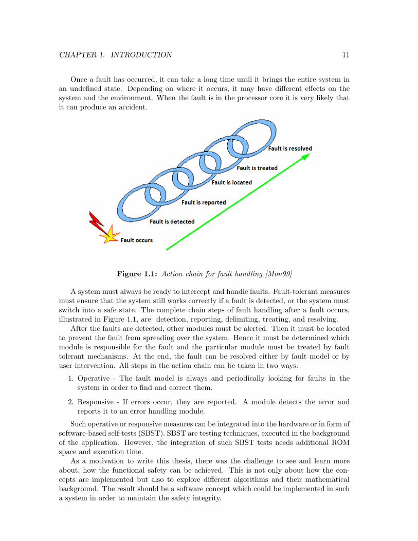
Once a fault has occurred, it can take a long time until it brings the entire system inan undefined state. Depending on where it occurs, it may have different effects on thesystem and the environment. When the fault is in the processor core it is very likely thatit can produce an accident.
Figure 1.1: Action chain for fault handling [Mon99]
A system must always be ready to intercept and handle faults. Fault-tolerant measuresmust ensure that the system still works correctly if a fault is detected, or the system mustswitch into a safe state. The complete chain steps of fault handling after a fault occurs,illustrated in Figure 1.1, are: detection, reporting, delimiting, treating, and resolving.
After the faults are detected, other modules must be alerted. Then it must be locatedto prevent the fault from spreading over the system. Hence it must be determined whichmodule is responsible for the fault and the particular module must be treated by faulttolerant mechanisms. At the end, the fault can be resolved either by fault model or byuser intervention. All steps in the action chain can be taken in two ways:
1. Operative - The fault model is always and periodically looking for faults in thesystem in order to find and correct them.
2. Responsive - If errors occur, they are reported. A module detects the error andreports it to an error handling module.
Such operative or responsive measures can be integrated into the hardware or in form ofsoftware-based self-tests (SBST). SBST are testing techniques, executed in the backgroundof the application. However, the integration of such SBST tests needs additional ROMspace and execution time.
As a motivation to write this thesis, there was the challenge to see and learn moreabout, how the functional safety can be achieved. This is not only about how the con-cepts are implemented but also to explore different algorithms and their mathematicalbackground. The result should be a software concept which could be implemented in sucha system in order to maintain the safety integrity.
CHAPTER 1. INTRODUCTION 12
During the preparation of this thesis, different multi-core microcontrollers for safety-relevant embedded systems which are available on the market were evaluated in terms ofsafety-related components, fault coverage and performance.
1.2 Objective
Designing an effective online testing strategy requires information about the architecture,RAM, ROM, instruction set, branch prediction etc. This information must be collectedand evaluated because in (E/E/PES) systems, failures can arise in different parts of thesystem, which are caused by hardware, software, electromagnetic or different influences.
For creating such an online-testing strategy, sufficient knowledge about the architectureof the system and different algorithms should be present. Hence, the first task of the thesiswas:
1. Study different safety strategies and architectures
2. Study different algorithms, their mathematical structure and fault models
3. Create a list of evaluation criteria based on which the microcontrollers will be eval-uated
4. Check which safety features and protection mechanisms that are implemented indifferent architectures
5. Based on the gained knowledge create a testing strategy
6. Implement the online periodic testing strategy and evaluate the results
After the evaluation task is finished, the online testing strategy which will be imple-mented to maintain the integrity of the system during runtime, the testing strategy wouldinvoke these functional properties defined in previous tasks. This means that as a part ofthe strategy, the support of hardware tests will be included.
At the end, the gained knowledge will form an on-line periodic strategy where the testswhich are developed must collaborate with each other to run in the background duringruntime and the application will perform its normal operation.
1.3 Structure
The second chapter gives a detailed introduction to the field of safety-related concepts,architectures and software-based self-tests. Fail-safe safety strategies are used to achievea safe state in case of a fault. Therefore, online fault detection is necessary.
Safety architectures are created using different algorithms which are proofs of conceptin the field and provide safety using redundant hardware components that minimize thecauses of common cause failures (CCF).
Software-based self tests (SBST) are described which are part of a solution to providesafety using the functional and structural information of microcontrollers. Using thisinformation, tests are generated and applied to cover faults which can cause unsafe states.
CHAPTER 1. INTRODUCTION 13
At the end of the chapter, the state of the art in the field of RAM testing algorithmsare described starting from the mathematical background, complexity, and execution time.
The third chapter describes the different architectures which are evaluated and basedon the evaluation criteria; a concept is built to cover the faults during runtime in theTMS570 microcontroller. The concept is an online strategy which consists of hardwareand software tests.
Chapter four presents the implementation of the concept described in the fourth chap-ter. This chapter covers the evaluation board and the tool chain which are used for thedevelopment, and each test is described regarding the implementation, execution time andfault injection.
Chapter five presents the conclusion of this thesis and prospects for future work.
Chapter 2
Related Work
2.1 Hardware architectures and strategies
2.1.1 Faults and Failures
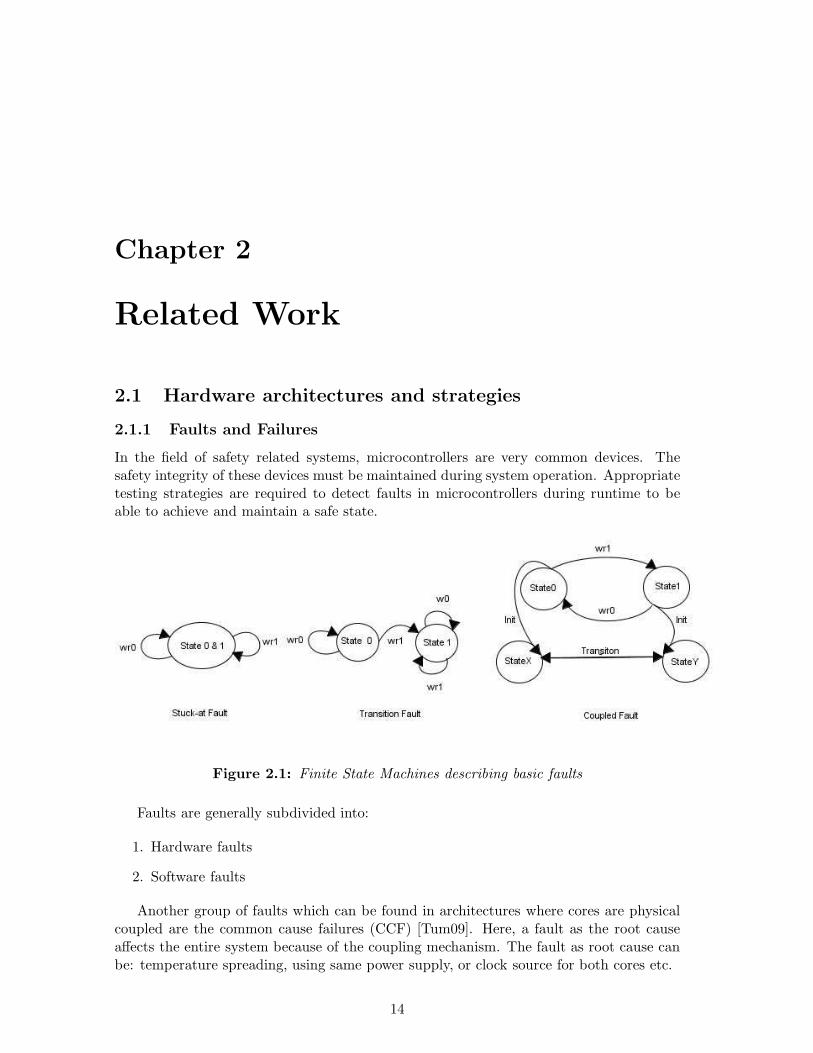
In the field of safety related systems, microcontrollers are very common devices. Thesafety integrity of these devices must be maintained during system operation. Appropriatetesting strategies are required to detect faults in microcontrollers during runtime to beable to achieve and maintain a safe state.
Figure 2.1: Finite State Machines describing basic faults
Faults are generally subdivided into:
1. Hardware faults
2. Software faults
Another group of faults which can be found in architectures where cores are physicalcoupled are the common cause failures (CCF) [Tum09]. Here, a fault as the root causeaffects the entire system because of the coupling mechanism. The fault as root cause canbe: temperature spreading, using same power supply, or clock source for both cores etc.
14
CHAPTER 2. RELATED WORK 15
Dependent on which part of the microcontroller the faults occur, they are called asfollows:
1. CPU Faults
• Arithmetic faults
• Logical faults
• Conditional faults
2. RAM Faults
• Stuck at faults
• Transition faults
• Coupling faults
3. Peripheral Faults
The arithmetical faults cause the ALU to perform calculations incorrectly. This canbe multiplication, addition, division etc. Logical and conditional faults are the reasonthat comparisons and jumps in programs are not performed correctly and can cause aninstruction routine jump elsewhere than intended.
But the most important faults which must be avoided in a system are RAM faults.Any single bit fault in a RAM cell can be a root cause for other failures in the systemsuch as previously described CPU faults.
Stuck-at faults(SAF) can occur in two forms: stuck at 0 and 1. As illustrated in thefinite state machine, stuck at 0 or 1 means that any attempt to change the state of a RAMcell from 0 to 1 or vice versa fails and the cell holds the original value.
Transition faults(TF) prevent a cell from changing its actual state from 0 to 1 or 1 to0. The difference between transition faults and stuck at faults are that, transition faultsaffect just one side of the state transition.
Coupling faults(CF) ensure that any transition in one RAM cell from one state toanother causes the changing of their actual state to one or to many other cells.
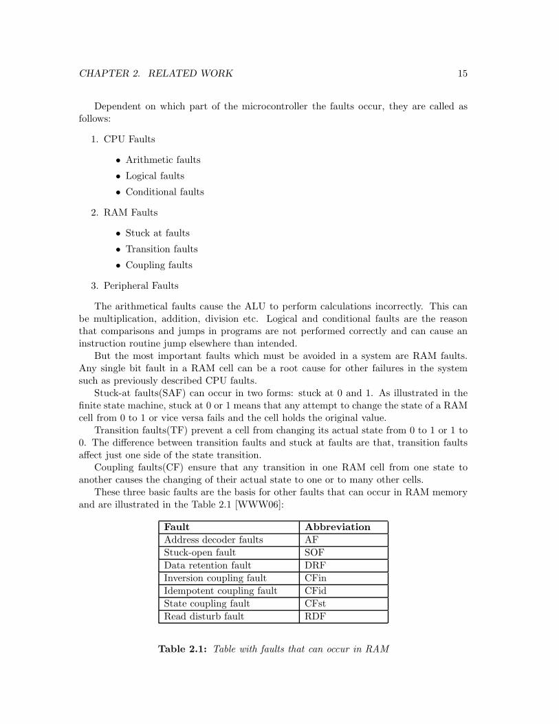
These three basic faults are the basis for other faults that can occur in RAM memoryand are illustrated in the Table 2.1 [WWW06]:
Fault Abbreviation
Address decoder faults AF
Stuck-open fault SOF
Data retention fault DRF
Inversion coupling fault CFin
Idempotent coupling fault CFid
State coupling fault CFst
Read disturb fault RDF
Table 2.1: Table with faults that can occur in RAM
CHAPTER 2. RELATED WORK 16
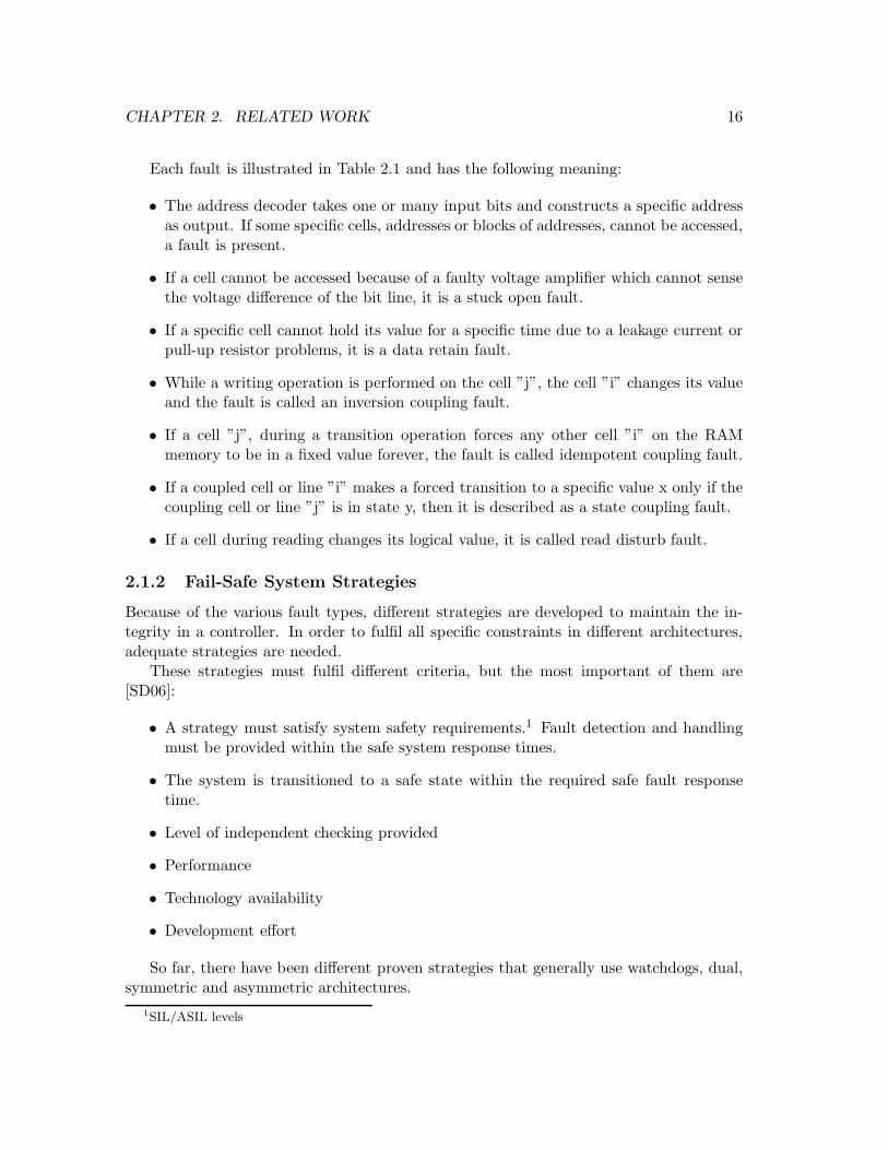
Each fault is illustrated in Table 2.1 and has the following meaning:
• The address decoder takes one or many input bits and constructs a specific addressas output. If some specific cells, addresses or blocks of addresses, cannot be accessed,a fault is present.
• If a cell cannot be accessed because of a faulty voltage amplifier which cannot sensethe voltage difference of the bit line, it is a stuck open fault.
• If a specific cell cannot hold its value for a specific time due to a leakage current orpull-up resistor problems, it is a data retain fault.
• While a writing operation is performed on the cell ”j”, the cell ”i” changes its valueand the fault is called an inversion coupling fault.
• If a cell ”j”, during a transition operation forces any other cell ”i” on the RAMmemory to be in a fixed value forever, the fault is called idempotent coupling fault.
• If a coupled cell or line ”i” makes a forced transition to a specific value x only if thecoupling cell or line ”j” is in state y, then it is described as a state coupling fault.
• If a cell during reading changes its logical value, it is called read disturb fault.
2.1.2 Fail-Safe System Strategies
Because of the various fault types, different strategies are developed to maintain the in-tegrity in a controller. In order to fulfil all specific constraints in different architectures,adequate strategies are needed.
These strategies must fulfil different criteria, but the most important of them are[SD06]:
• A strategy must satisfy system safety requirements.1 Fault detection and handlingmust be provided within the safe system response times.
• The system is transitioned to a safe state within the required safe fault responsetime.
• Level of independent checking provided
• Performance
• Technology availability
• Development effort
So far, there have been different proven strategies that generally use watchdogs, dual,symmetric and asymmetric architectures.
1SIL/ASIL levels
CHAPTER 2. RELATED WORK 17
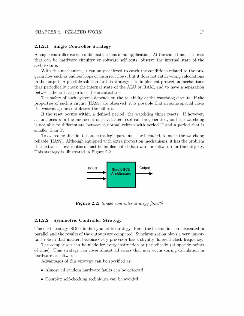
2.1.2.1 Single Controller Strategy
A single controller executes the instructions of an application. At the same time, self-teststhat can be hardware circuitry or software self tests, observe the internal state of thearchitecture.
With this mechanism, it can only achieved to catch the conditions related to the pro-gram flow such as endless loops or incorrect flows, but it does not catch wrong calculationsin the output. A possible solution for this strategy is to implement protection mechanismsthat periodically check the internal state of the ALU or RAM, and to have a separationbetween the critical parts of the architecture.
The safety of such systems depends on the reliability of the watchdog circuits. If theproperties of such a circuit [HA99] are observed, it is possible that in some special casesthe watchdog does not detect the failures.
If the reset occurs within a defined period, the watchdog timer reacts. If however,a fault occurs in the microcontroller, a faster reset can be generated, and the watchdogis not able to differentiate between a normal refresh with period T and a period that issmaller than T.
To overcome this limitation, extra logic parts must be included, to make the watchdogreliable [HA99]. Although equipped with extra protection mechanisms, it has the problemthat extra self-test routines must be implemented (hardware or software) for the integrity.This strategy is illustrated in Figure 2.2.
Figure 2.2: Single controller strategy [SD06]
2.1.2.2 Symmetric Controller Strategy
The next strategy [SD06] is the symmetric strategy. Here, the instructions are executed inparallel and the results of the outputs are compared. Synchronization plays a very impor-tant role in that matter, because every processor has a slightly different clock frequency.
The comparison can be made for every instruction or periodically (at specific pointsof time). This strategy can cover almost all errors that may occur during calculation inhardware or software.
Advantages of this strategy can be specified as:
• Almost all random hardware faults can be detected
• Complex self-checking techniques can be avoided
CHAPTER 2. RELATED WORK 18
Disadvantages or limitations:
• Both processors must be synchronized
• Large size and cost because the architecture has two processors
Figure 2.3: Symmetric controller strategy [SD06]
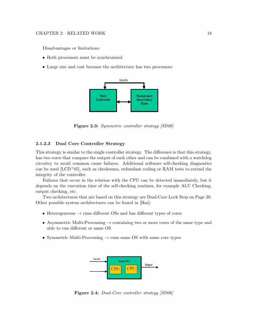
2.1.2.3 Dual Core Controller Strategy
This strategy is similar to the single controller strategy. The difference is that this strategy,has two cores that compare the output of each other and can be combined with a watchdogcircuitry to avoid common cause failures. Additional software self-checking diagnosticscan be used [LCD+05], such as checksums, redundant coding or RAM tests to extend theintegrity of the controller.
Failures that occur in the relation with the CPU can be detected immediately, but itdepends on the execution time of the self-checking routines, for example ALU Checking,output checking, etc.
Two architectures that are based on this strategy are Dual-Core Lock Step on Page 20.Other possible system architectures can be found in [Has]:
• Heterogeneous → runs different OSs and has different types of cores
• Asymmetric Multi-Processing → containing two or more cores of the same type andable to run different or same OS
• Symmetric Multi-Processing → runs same OS with same core types
Figure 2.4: Dual-Core controller strategy [SD06]
CHAPTER 2. RELATED WORK 19
2.1.2.4 Asymmetric Controller Strategy
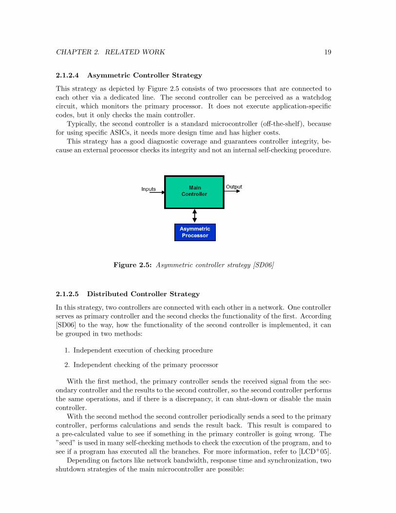
This strategy as depicted by Figure 2.5 consists of two processors that are connected toeach other via a dedicated line. The second controller can be perceived as a watchdogcircuit, which monitors the primary processor. It does not execute application-specificcodes, but it only checks the main controller.
Typically, the second controller is a standard microcontroller (off-the-shelf), becausefor using specific ASICs, it needs more design time and has higher costs.
This strategy has a good diagnostic coverage and guarantees controller integrity, be-cause an external processor checks its integrity and not an internal self-checking procedure.
Figure 2.5: Asymmetric controller strategy [SD06]
2.1.2.5 Distributed Controller Strategy
In this strategy, two controllers are connected with each other in a network. One controllerserves as primary controller and the second checks the functionality of the first. According[SD06] to the way, how the functionality of the second controller is implemented, it canbe grouped in two methods:
1. Independent execution of checking procedure
2. Independent checking of the primary processor
With the first method, the primary controller sends the received signal from the sec-ondary controller and the results to the second controller, so the second controller performsthe same operations, and if there is a discrepancy, it can shut-down or disable the maincontroller.
With the second method the second controller periodically sends a seed to the primarycontroller, performs calculations and sends the result back. This result is compared toa pre-calculated value to see if something in the primary controller is going wrong. The”seed” is used in many self-checking methods to check the execution of the program, and tosee if a program has executed all the branches. For more information, refer to [LCD+05].
Depending on factors like network bandwidth, response time and synchronization, twoshutdown strategies of the main microcontroller are possible:
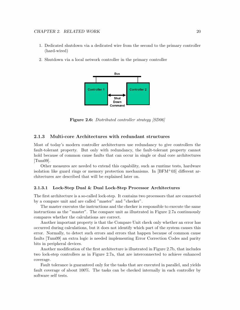
CHAPTER 2. RELATED WORK 20
1. Dedicated shutdown via a dedicated wire from the second to the primary controller(hard-wired)
2. Shutdown via a local network controller in the primary controller
Figure 2.6: Distributed controller strategy [SD06]
2.1.3 Multi-core Architectures with redundant structures
Most of today’s modern controller architectures use redundancy to give controllers thefault-tolerant property. But only with redundancy, the fault-tolerant property cannothold because of common cause faults that can occur in single or dual core architectures[Tum09].
Other measures are needed to extend this capability, such as runtime tests, hardwareisolation like guard rings or memory protection mechanisms. In [BFM+03] different ar-chitectures are described that will be explained later on.
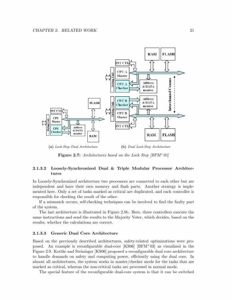
2.1.3.1 Lock-Step Dual & Dual Lock-Step Processor Architectures
The first architecture is a so-called lock-step. It contains two processors that are connectedby a compare unit and are called ”master” and ”checker”.
The master executes the instructions and the checker is responsible to execute the sameinstructions as the ”master”. The compare unit as illustrated in Figure 2.7a continuouslycompares whether the calculations are correct.
Another important property is that the Compare Unit check only whether an error hasoccurred during calculations, but it does not identify which part of the system causes thiserror. Normally, to detect such errors and errors that happen because of common causefaults [Tum09] an extra logic is needed implementing Error Correction Codes and paritybits in peripheral devices.
Another modification of the first architecture is illustrated in Figure 2.7b, that includestwo lock-step controllers as in Figure 2.7a, that are interconnected to achieve enhancedcoverage.
Fault tolerance is guaranteed only for the tasks that are executed in parallel, and yieldsfault coverage of about 100%. The tasks can be checked internally in each controller bysoftware self tests.
CHAPTER 2. RELATED WORK 21
(a) Lock-Step Dual Architecture (b) Dual Lock-Step Architecture
Figure 2.7: Architectures based on the Lock Step [BFM+03]
2.1.3.2 Loosely-Synchronized Dual & Triple Modular Processor Architec-tures
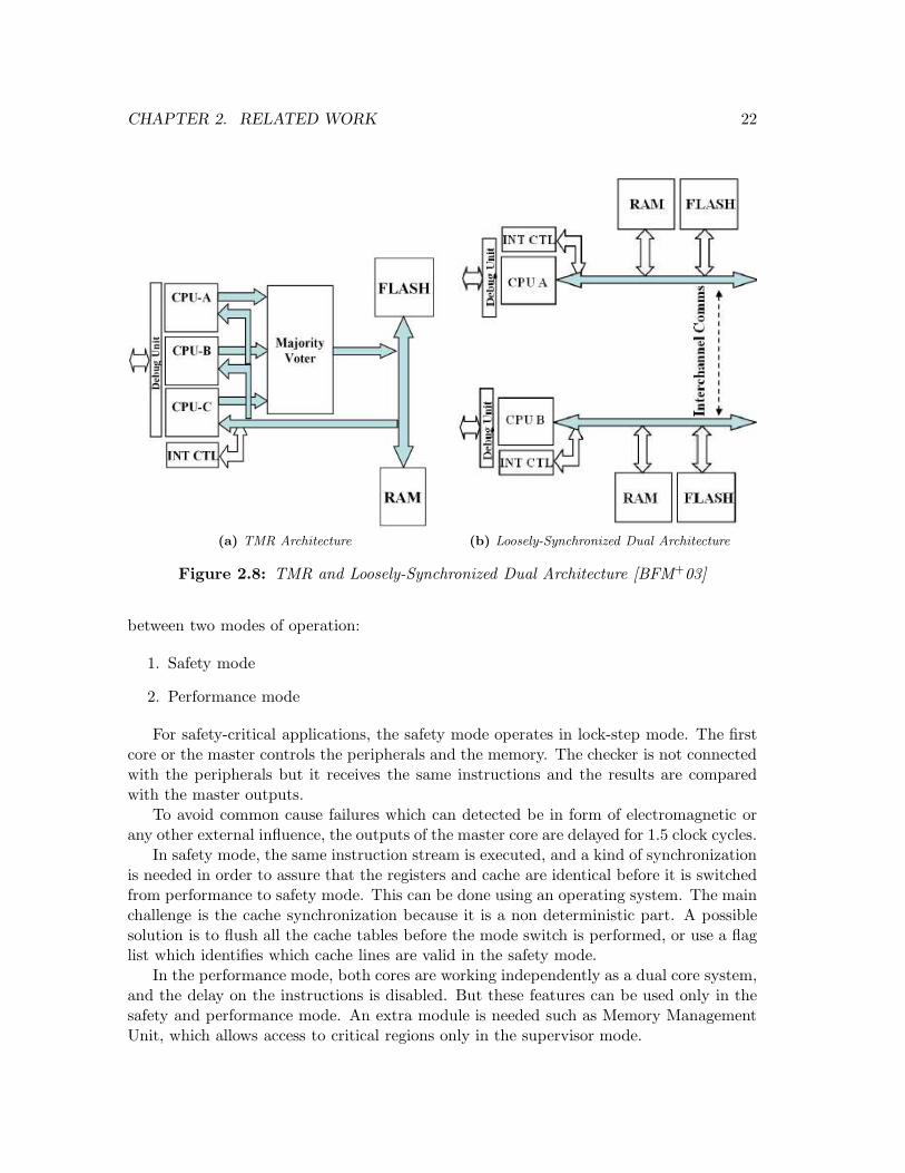
In Loosely-Synchronized architecture two processors are connected to each other but areindependent and have their own memory and flash parts. Another strategy is imple-mented here. Only a set of tasks marked as critical are duplicated, and each controller isresponsible for checking the result of the other.
If a mismatch occurs, self-checking techniques can be involved to find the faulty partof the system.
The last architecture is illustrated in Figure 2.8b. Here, three controllers execute thesame instructions and send the results to the Majority Voter, which decides, based on theresults, whether the calculations are correct.
2.1.3.3 Generic Dual Core Architecture
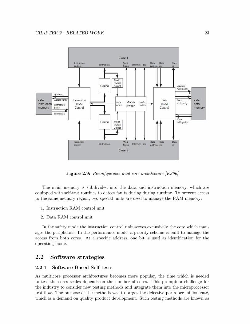
Based on the previously described architectures, safety-related optimizations were pro-posed. An example is reconfigurable dual-core [KS06] [BFM+03] as visualized in theFigure 2.9. Kottke and Steininger [KS06] proposed a reconfigurable dual core architectureto handle demands on safety and computing power, efficiently using the dual core. Inalmost all architectures, the system works in master/checker mode for the tasks that aremarked as critical, whereas the non-critical tasks are processed in normal mode.
The special feature of the reconfigurable dual-core system is that it can be switched
CHAPTER 2. RELATED WORK 22
(a) TMR Architecture (b) Loosely-Synchronized Dual Architecture
Figure 2.8: TMR and Loosely-Synchronized Dual Architecture [BFM+03]
between two modes of operation:
1. Safety mode
2. Performance mode
For safety-critical applications, the safety mode operates in lock-step mode. The firstcore or the master controls the peripherals and the memory. The checker is not connectedwith the peripherals but it receives the same instructions and the results are comparedwith the master outputs.
To avoid common cause failures which can detected be in form of electromagnetic orany other external influence, the outputs of the master core are delayed for 1.5 clock cycles.
In safety mode, the same instruction stream is executed, and a kind of synchronizationis needed in order to assure that the registers and cache are identical before it is switchedfrom performance to safety mode. This can be done using an operating system. The mainchallenge is the cache synchronization because it is a non deterministic part. A possiblesolution is to flush all the cache tables before the mode switch is performed, or use a flaglist which identifies which cache lines are valid in the safety mode.
In the performance mode, both cores are working independently as a dual core system,and the delay on the instructions is disabled. But these features can be used only in thesafety and performance mode. An extra module is needed such as Memory ManagementUnit, which allows access to critical regions only in the supervisor mode.
CHAPTER 2. RELATED WORK 23
Figure 2.9: Reconfigurable dual core architecture [KS06]
The main memory is subdivided into the data and instruction memory, which areequipped with self-test routines to detect faults during during runtime. To prevent accessto the same memory region, two special units are used to manage the RAM memory:
1. Instruction RAM control unit
2. Data RAM control unit
In the safety mode the instruction control unit serves exclusively the core which man-ages the peripherals. In the performance mode, a priority scheme is built to manage theaccess from both cores. At a specific address, one bit is used as identification for theoperating mode.
2.2 Software strategies
2.2.1 Software Based Self tests
As multicore processor architectures becomes more popular, the time which is neededto test the cores scales depends on the number of cores. This prompts a challenge forthe industry to consider new testing methods and integrate them into the microprocessortest flow. The purpose of the methods was to target the defective parts per million rate,which is a demand on quality product development. Such testing methods are known as
CHAPTER 2. RELATED WORK 24
functional self testing (instruction-based self testing) or commonly ”software-based self-testing” [WWC+05].
”The key idea of SBST is to exploit on chip programmable resources to run normalprograms that test the processor itself” [WWC+05]. Some SBST tests, exploit the instruc-tion set of the Architecture and performs safety critical checks in the background usingthe actual clock frequency.
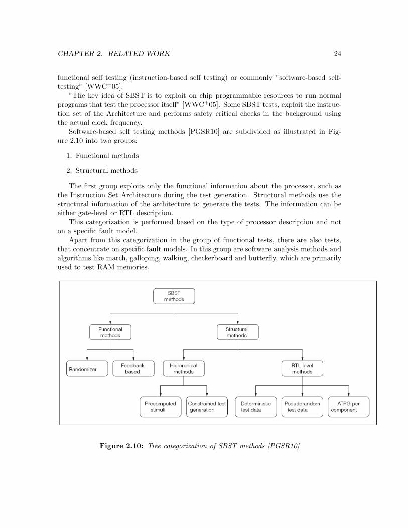
Software-based self testing methods [PGSR10] are subdivided as illustrated in Fig-ure 2.10 into two groups:
1. Functional methods
2. Structural methods
The first group exploits only the functional information about the processor, such asthe Instruction Set Architecture during the test generation. Structural methods use thestructural information of the architecture to generate the tests. The information can beeither gate-level or RTL description.
This categorization is performed based on the type of processor description and noton a specific fault model.
Apart from this categorization in the group of functional tests, there are also tests,that concentrate on specific fault models. In this group are software analysis methods andalgorithms like march, galloping, walking, checkerboard and butterfly, which are primarilyused to test RAM memories.
Figure 2.10: Tree categorization of SBST methods [PGSR10]
CHAPTER 2. RELATED WORK 25
2.2.2 Functional Tests
Functional tests as illustrated in Figure 2.10 based on the logic they use are subdividedinto two groups:
1. Randomized - generate tests with specific constraints during runtime
2. Feedback based - evaluate previous results to be considered for the new test gener-ation during development time
Good representatives for the randomized tests are the methods defined in:
• VERTIS [SA98]
• FRITS [PML02]
• Load & GO [BHW06]
VERTIS uses the instruction set from the Programmers’ Manual to extract the infor-mation about the functionality of the processor. This information is grouped and writtenin a predefined format that can be used by the generation tool. This file format can befound in [SA98]. The test generated from the tool is pseudo assembler and can be adoptedeasily for different architectures.
VERTIS can generate data randomly or as specified by the user which are used fordifferent processor instructions. With the generated test sequences different parts of thesystem are tested from the functional view like: CPU, memory, fetching units etc.
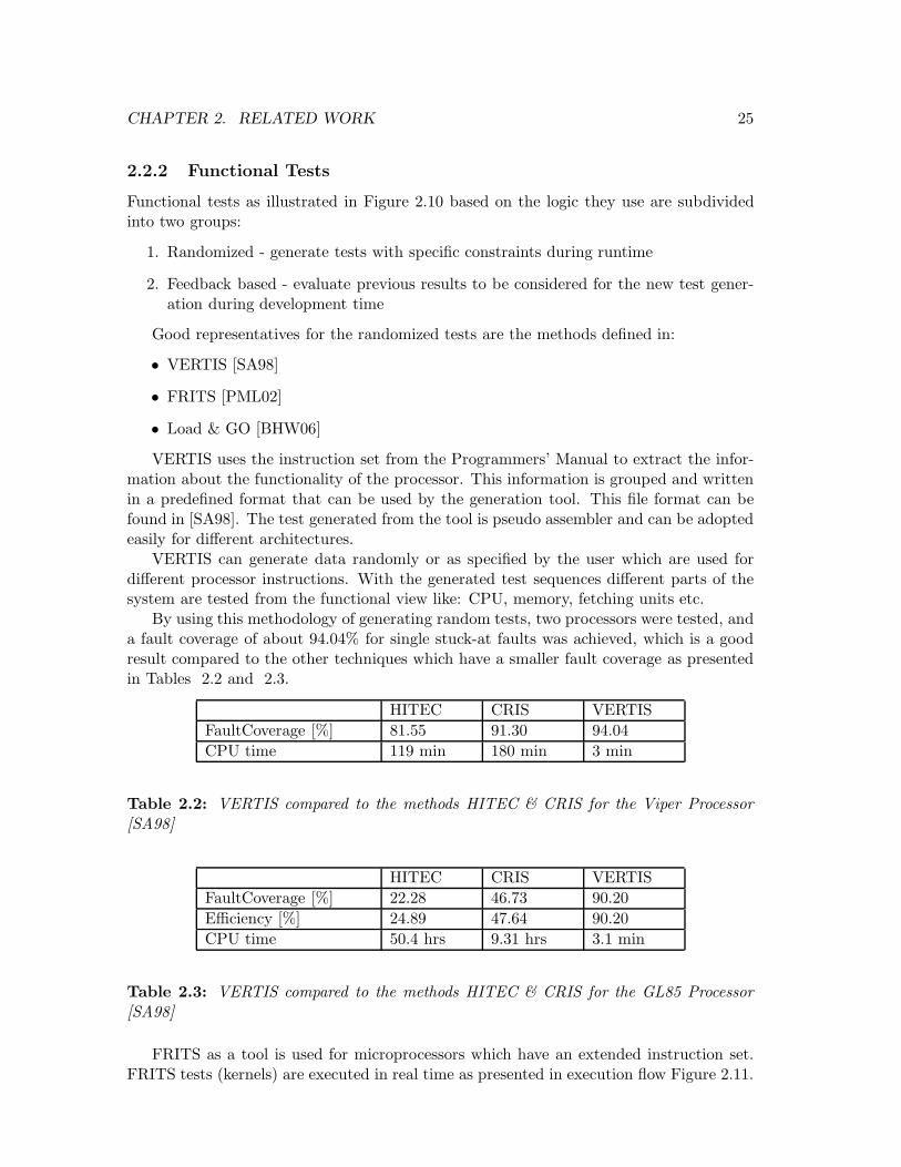
By using this methodology of generating random tests, two processors were tested, anda fault coverage of about 94.04% for single stuck-at faults was achieved, which is a goodresult compared to the other techniques which have a smaller fault coverage as presentedin Tables 2.2 and 2.3.
HITEC CRIS VERTIS
FaultCoverage [%] 81.55 91.30 94.04
CPU time 119 min 180 min 3 min
Table 2.2: VERTIS compared to the methods HITEC & CRIS for the Viper Processor[SA98]
HITEC CRIS VERTIS
FaultCoverage [%] 22.28 46.73 90.20
Efficiency [%] 24.89 47.64 90.20
CPU time 50.4 hrs 9.31 hrs 3.1 min
Table 2.3: VERTIS compared to the methods HITEC & CRIS for the GL85 Processor[SA98]
FRITS as a tool is used for microprocessors which have an extended instruction set.FRITS tests (kernels) are executed in real time as presented in execution flow Figure 2.11.
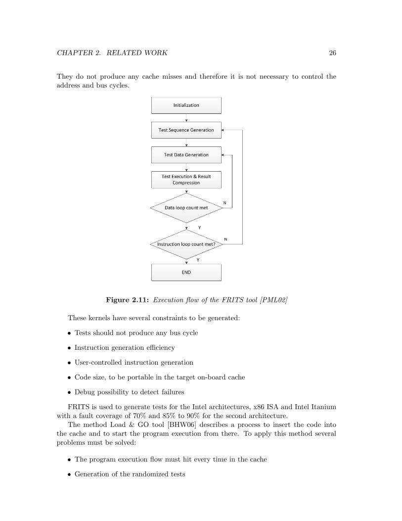
CHAPTER 2. RELATED WORK 26
They do not produce any cache misses and therefore it is not necessary to control theaddress and bus cycles.
Figure 2.11: Execution flow of the FRITS tool [PML02]
These kernels have several constraints to be generated:
• Tests should not produce any bus cycle
• Instruction generation efficiency
• User-controlled instruction generation
• Code size, to be portable in the target on-board cache
• Debug possibility to detect failures
FRITS is used to generate tests for the Intel architectures, x86 ISA and Intel Itaniumwith a fault coverage of 70% and 85% to 90% for the second architecture.
The method Load & GO tool [BHW06] describes a process to insert the code intothe cache and to start the program execution from there. To apply this method severalproblems must be solved:
• The program execution flow must hit every time in the cache
• Generation of the randomized tests
CHAPTER 2. RELATED WORK 27
• To catch the results of the test (passed or failed)
For the proof of concept the UltraSPARC microprocessor was used, which shows thateven with all simulations and test optimization this architecture lacks non-determinism ofthe flow.
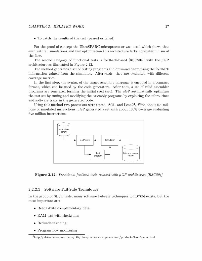
The second category of functional tests is feedback-based [RSCS04], with the µGParchitecture as illustrated in Figure 2.12.
The method generates a set of testing programs and optimizes them using the feedbackinformation gained from the simulator. Afterwards, they are evaluated with differentcoverage metrics.
In the first step, the syntax of the target assembly language is encoded in a compactformat, which can be used by the code generators. After that, a set of valid assemblerprograms are generated forming the initial seed (set). The µGP automatically optimizesthe test set by tuning and modifying the assembly programs by exploiting the subroutinesand software traps in the generated code.
Using this method two processors were tested, i8051 and Leon22. With about 8.4 mil-lions of simulated instructions, µGP generated a set with about 100% coverage evaluatingfive million instructions.
Figure 2.12: Functional feedback tests realized with µGP architecture [RSCS04]
2.2.2.1 Software Fail-Safe Techniques
In the group of SBST tests, many software fail-safe techniques [LCD+05] exists, but themost important are:
• Read/Write complementary data
• RAM test with checksums
• Redundant coding
• Program flow monitoring
2http://vlsicad.eecs.umich.edu/BK/Slots/cache/www.gaisler.com/products/leon2/leon.html
CHAPTER 2. RELATED WORK 28
Working with complementary data it is the first basic technique. Specific data iswritten in a part of the memory, the one’s complement is calculated and stored in aseparate part of the system. Checking whether a fault has occurred in the memory isdone by the summation of these two values. The result should be zero. This checking canbe done periodically or randomly based on the testing strategy. The main limitation ofthis technique is the RAM size, because in order to store every complementary value, aseparate storage is needed.
RAM tests are performed to assure that data can be held and manipulated withouterrors. RAM tests can be done during system initialization, before the program is running,or during runtime, online periodically.
Checksums can be used to check the integrity of ROM, Flash, or EEPROM. For systemvalues that do not change at runtime, the checksum can be calculated and stored in ROM.But checking the entire ROM needs many cycles, and that requires time. Testing theEEPROM is faster. An approach to reduce testing time is to check only the pieces thatare marked as safety-critical. Checksums can find faults like memory errors, bit flips, andother data changes.
Redundant coding is a technique to implement, store, and run the same safety-criticalcode in different pieces of memory. For the same input, the result should be every timethe same. It is a software protection method which needs extra implementation to assurethat the code fragments do not have access to the same data and that the program itselfruns correctly. The last technique is the program flow monitoring.
Program flow monitoring (PFM) is a technique to include a specific seed/key valuesprogram flow. With the help of these two values, it can be checked whether the programhas executed all steps. These values can be inserted between function calls, or can beintegrated into the program structure. Based on how the PFM values are included, thePFM can be implemented in the following ways:
1. Application-independent
2. Application-dependent
3. Time-dependent
The application-independent method updates the values between each function call. Adisadvantage of this method is that the value can be updated without execution of thefunction. The advantage is that the PFM code can be reused without the modificationacross the application.
The application-dependent PFM is tightly integrated into the program execution. Theupdate of the value is performed within the function, and assures that all functions arecalled.
The time-dependent PFM helps to verify that specific functions are called within arequired timing window. This is accomplished by updating the values at specific times,during program execution.
2.2.2.2 March Tests
March tests [BBC+08], [Goo93] form a group of tests which exist in different variationsthat are simple and have linear complexity O(n).
CHAPTER 2. RELATED WORK 29
The basic operation in all variations is called ”march element”. Every march elementcontains basic operations which are performed in a cell and then proceeds to the next cell:
• Writing 0 into the cell - w0
• Reading expected 0 from the cell - r0
• Writing 1 into the cell - w1
• Reading expected 1 from the cell - r1
After these operations are performed in a cell, the next cell is selected with increasing(⇑) or decreasing(⇓) address order. The symbol (m) is used if the addressing order is notimportant.
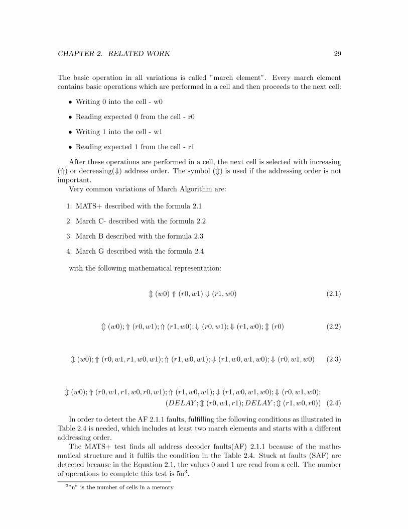
Very common variations of March Algorithm are:
1. MATS+ described with the formula 2.1
2. March C- described with the formula 2.2
3. March B described with the formula 2.3
4. March G described with the formula 2.4
with the following mathematical representation:
m (w0) ⇑ (r0, w1) ⇓ (r1, w0) (2.1)
m (w0);⇑ (r0, w1);⇑ (r1, w0);⇓ (r0, w1);⇓ (r1, w0);m (r0) (2.2)
m (w0);⇑ (r0, w1, r1, w0, w1);⇑ (r1, w0, w1);⇓ (r1, w0, w1, w0);⇓ (r0, w1, w0) (2.3)
m (w0);⇑ (r0, w1, r1, w0, r0, w1);⇑ (r1, w0, w1);⇓ (r1, w0, w1, w0);⇓ (r0, w1, w0);
(DELAY ;m (r0, w1, r1);DELAY ;m (r1, w0, r0)) (2.4)
In order to detect the AF 2.1.1 faults, fulfilling the following conditions as illustrated inTable 2.4 is needed, which includes at least two march elements and starts with a differentaddressing order.
The MATS+ test finds all address decoder faults(AF) 2.1.1 because of the mathe-matical structure and it fulfils the condition in the Table 2.4. Stuck at faults (SAF) aredetected because in the Equation 2.1, the values 0 and 1 are read from a cell. The numberof operations to complete this test is 5n3.
3”n” is the number of cells in a memory
CHAPTER 2. RELATED WORK 30
Condition March element
1 ⇑ (rx, ...wx)
2 ⇓ (rx, ...wx)
Table 2.4: Two conditions for a test to detect the AF Faults
The MarchC- test is an extension of the MarchC, which has linear complexity O(n)and requires 10n operations to complete the test. Three groups of faults are targetedwith this test: AF because it satisfies the conditions in Table 2.4, SAF because in theequation 2.2, it reads 1 and 0 from the cells and all CFin and CFSsts faults are detecteddue to the successively read and write operations.
The MarchB test which requires 17n operations, targets and detects the followingfaults: all AFs, SAFs, TFs, CFins and linked CFids, described in Section 2.1.1.
Condition March element
1 ..., rx, ...rx
2 ..., rx, ...rx
Table 2.5: Two conditions for a test to detect the COF Faults
A COF Fault is present if a specific RAM cell cannot be accessed. To ensure that everycell is accessible, it must be guaranteed that 0 and 1 is read from the cell as illustrated inTable 2.5. To extend a march test to allow the detection of DRF faults as well, it mustcontain delays between writing a value ”x” and reading it back.
The MarchG test is an extension of the MarchB test which includes these two exten-sions and specifically detects COF and DRF faults. To complete the test it requires 23n+ 2Del4 operations.
2.2.2.3 Abraham Test
Another functional test for RAM memory is the Abraham Test. In order to apply thetest, there need not be structural information about the processor and covers specificallystuck at faults and coupled faults. It not only covers these faults but it covers the faultsthat occur in different parts of the RAM:
1. Memory Cell Array,
2. Read/Write Logic and
3. Decoder Logic
4Delayed operations
CHAPTER 2. RELATED WORK 31
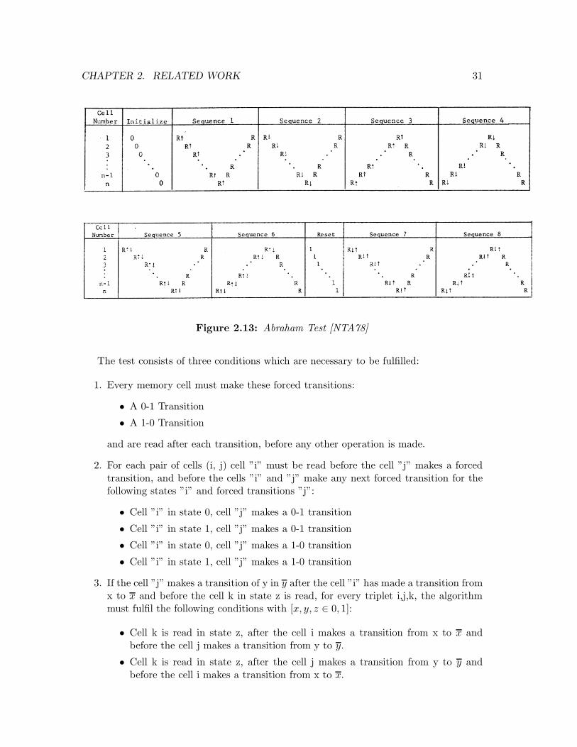
Figure 2.13: Abraham Test [NTA78]
The test consists of three conditions which are necessary to be fulfilled:
1. Every memory cell must make these forced transitions:
• A 0-1 Transition
• A 1-0 Transition
and are read after each transition, before any other operation is made.
2. For each pair of cells (i, j) cell ”i” must be read before the cell ”j” makes a forcedtransition, and before the cells ”i” and ”j” make any next forced transition for thefollowing states ”i” and forced transitions ”j”:
• Cell ”i” in state 0, cell ”j” makes a 0-1 transition
• Cell ”i” in state 1, cell ”j” makes a 0-1 transition
• Cell ”i” in state 0, cell ”j” makes a 1-0 transition
• Cell ”i” in state 1, cell ”j” makes a 1-0 transition
3. If the cell ”j” makes a transition of y in y after the cell ”i” has made a transition fromx to x and before the cell k in state z is read, for every triplet i,j,k, the algorithmmust fulfil the following conditions with [x, y, z ∈ 0, 1]:
• Cell k is read in state z, after the cell i makes a transition from x to x andbefore the cell j makes a transition from y to y.
• Cell k is read in state z, after the cell j makes a transition from y to y andbefore the cell i makes a transition from x to x.
CHAPTER 2. RELATED WORK 32
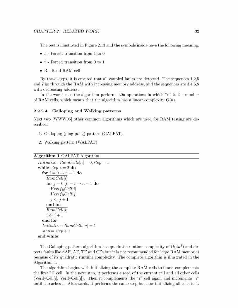
The test is illustrated in Figure 2.13 and the symbols inside have the following meaning:
• ↓ - Forced transition from 1 to 0
• ↑ - Forced transition from 0 to 1
• R - Read RAM cell
By these steps, it is ensured that all coupled faults are detected. The sequences 1,2,5and 7 go through the RAM with increasing memory address, and the sequences are 3,4,6,8with decreasing address.
In the worst case the algorithm performs 30n operations in which ”n” is the numberof RAM cells, which means that the algorithm has a linear complexity O(n).
2.2.2.4 Galloping and Walking patterns
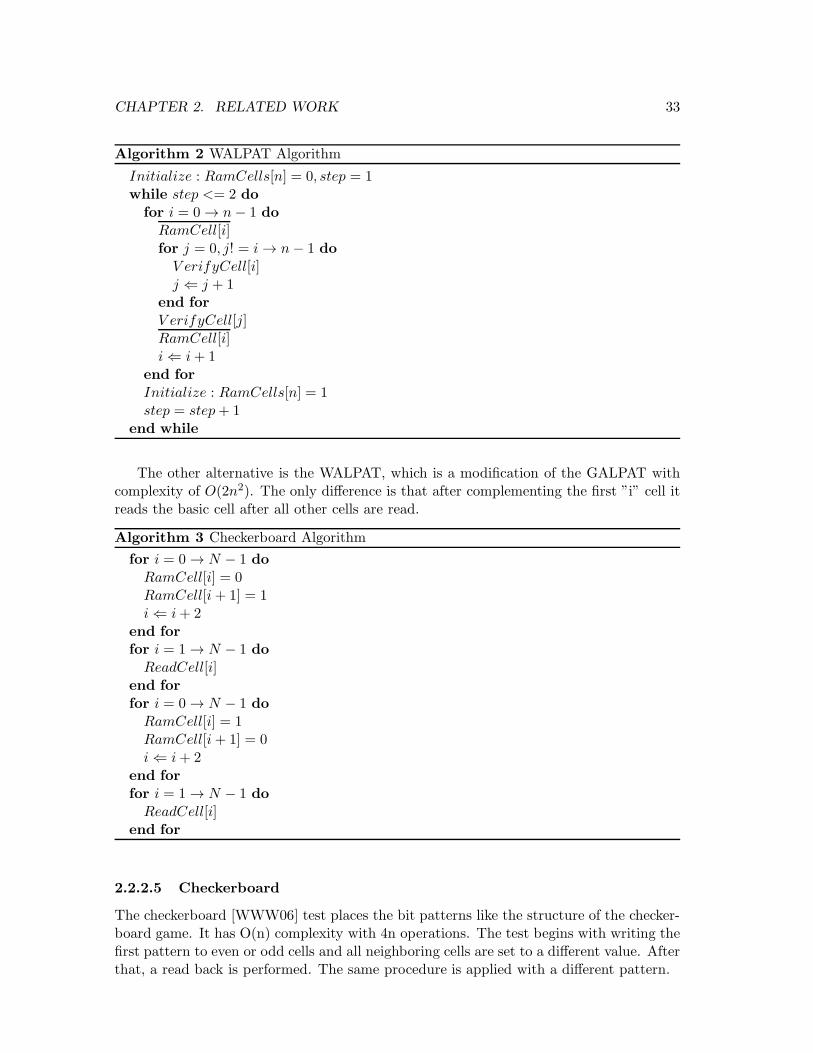
Next two [WWW06] other common algorithms which are used for RAM testing are de-scribed:
1. Galloping (ping-pong) pattern (GALPAT)
2. Walking pattern (WALPAT)
Algorithm 1 GALPAT Algorithm
Initialize : RamCells[n] = 0, step = 1while step <= 2 do
for i = 0 → n− 1 doRamCell[i]for j = 0, j! = i → n− 1 do
V erifyCell[i]V erifyCell[j]j ⇐ j + 1
end forRamCell[i]i ⇐ i+ 1
end forInitialize : RamCells[n] = 1step = step+ 1
end while
The Galloping pattern algorithm has quadratic runtime complexity of O(4n2) and de-tects faults like SAF, AF, TF and CFs but it is not recommended for large RAM memoriesbecause of its quadratic runtime complexity. The complete algorithm is illustrated in theAlgorithm 1.
The algorithm begins with initializing the complete RAM cells to 0 and complementsthe first ”i” cell. In the next step, it performs a read of the current cell and all other cells(VerifyCell[i], VerifyCell[j]). Then it complements the ”i” cell again and increments ”i”until it reaches n. Afterwards, it performs the same step but now initializing all cells to 1.
CHAPTER 2. RELATED WORK 33
Algorithm 2 WALPAT Algorithm
Initialize : RamCells[n] = 0, step = 1while step <= 2 do
for i = 0 → n− 1 doRamCell[i]for j = 0, j! = i → n− 1 do
V erifyCell[i]j ⇐ j + 1
end forV erifyCell[j]RamCell[i]i ⇐ i+ 1
end forInitialize : RamCells[n] = 1step = step+ 1
end while
The other alternative is the WALPAT, which is a modification of the GALPAT withcomplexity of O(2n2). The only difference is that after complementing the first ”i” cell itreads the basic cell after all other cells are read.
Algorithm 3 Checkerboard Algorithm
for i = 0 → N − 1 doRamCell[i] = 0RamCell[i+ 1] = 1i ⇐ i+ 2
end forfor i = 1 → N − 1 do
ReadCell[i]end forfor i = 0 → N − 1 do
RamCell[i] = 1RamCell[i+ 1] = 0i ⇐ i+ 2
end forfor i = 1 → N − 1 do
ReadCell[i]end for
2.2.2.5 Checkerboard
The checkerboard [WWW06] test places the bit patterns like the structure of the checker-board game. It has O(n) complexity with 4n operations. The test begins with writing thefirst pattern to even or odd cells and all neighboring cells are set to a different value. Afterthat, a read back is performed. The same procedure is applied with a different pattern.
CHAPTER 2. RELATED WORK 34
It is mainly used just to activate different faults, and a delay is included between readand write operations. It targets but does not detect all AF, SAF, TF and CF faults.
2.2.2.6 Butterfly Algorithm
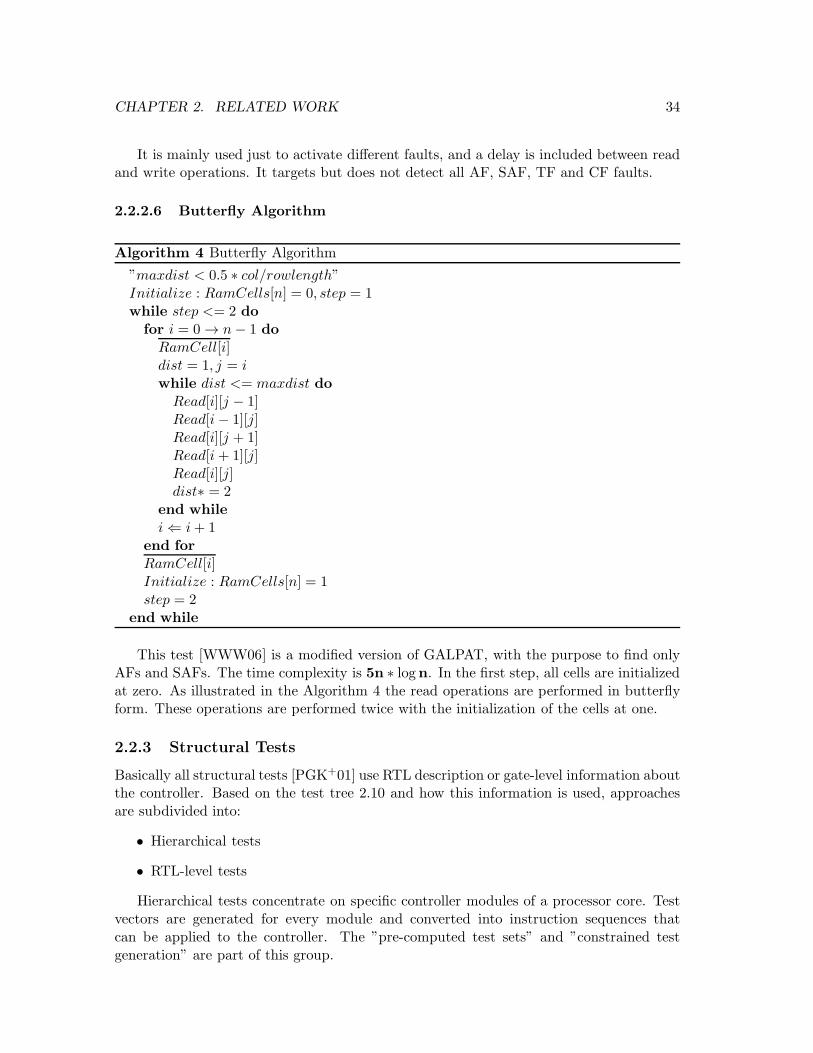
Algorithm 4 Butterfly Algorithm
”maxdist < 0.5 ∗ col/rowlength”Initialize : RamCells[n] = 0, step = 1while step <= 2 do
for i = 0 → n− 1 doRamCell[i]dist = 1, j = iwhile dist <= maxdist do
Read[i][j − 1]Read[i− 1][j]Read[i][j + 1]Read[i+ 1][j]Read[i][j]dist∗ = 2
end whilei ⇐ i+ 1
end forRamCell[i]Initialize : RamCells[n] = 1step = 2
end while
This test [WWW06] is a modified version of GALPAT, with the purpose to find onlyAFs and SAFs. The time complexity is 5n ∗ logn. In the first step, all cells are initializedat zero. As illustrated in the Algorithm 4 the read operations are performed in butterflyform. These operations are performed twice with the initialization of the cells at one.
2.2.3 Structural Tests
Basically all structural tests [PGK+01] use RTL description or gate-level information aboutthe controller. Based on the test tree 2.10 and how this information is used, approachesare subdivided into:
• Hierarchical tests
• RTL-level tests
Hierarchical tests concentrate on specific controller modules of a processor core. Testvectors are generated for every module and converted into instruction sequences thatcan be applied to the controller. The ”pre-computed test sets” and ”constrained testgeneration” are part of this group.
CHAPTER 2. RELATED WORK 35
”Pre-computed test sets” denotes a group of methods that generates stimuli sets forevery module of the controller under consideration, and then exploits the functional mecha-nism to give the module the precomputed stimuli and to propagate the results to observablelocations.
A representative is a method [GVA06] which generates test sequences with the mainfocus on functional faults that are difficult to detect. It involves controllability and ob-servability properties with Boolean differences and a bounded model checker.
To simulate faults difficult to detect, pseudo random instructions are generated with36579 instructions for the OpenRISC 1200 processor5 and using an available commercialtool. The fault coverage is evaluated which has a result of about 68% for stuck-at faults.
The list of undetected faults from the first step, is the basis for next step. A selec-tion process is performed to group the instructions based on the modules, and then, thecommercial ATPG tool generates for each module new test sequences. The observabilityproperties are guaranteed with the expression of propagation requirements as Booleandifferences.
The model checker evaluates the sequences to see which one propagates the effects ofthe observed fault to the primary output, and finally only these sequences remain. Thecomplete process on the OpenRISC 1200 processor increases the fault coverage by about14% to overall 82% for stuck-at faults.
Constrained test generation describes the modules on the processor with different ab-straction levels. The module under consideration is described at RTL level, whereas theother modules of the system are described at a higher level. With the detailed descriptionof only the module under consideration, the ATPG tool has a lower circuit complexitythan the original one.
Part of this group is the method proposed by Chen [CRRD03], which divides a givenprocessor up into different levels of modules, generates templates sets, and, using the con-trollability and observability properties, selects the most suitable templates. A constrainedtest generation is performed with selected templates and, for specific module, and at theend, the module test patterns are translated into instruction test sequences. Using thismethod for a RISC processor, a fault coverage of 95% was achieved for common faultslike stuck-at faults, but it can be applied to other fault models like bridging faults andtransistor-level faults.
SBST methods that use structural information (RTL) during the process of tests gen-eration are part of the RTL structural test branch as illustrated in Figure 2.10. Based onthe information which is used to generate test vectors, they are subdivided into:
• Deterministic algorithms
• ATPG Algorithms
• Pseudorandom methods
Deterministic algorithms use information about a specific function that a controllerperforms.
Kranitis [KPGX05] proposed a component-based divide and conquer approach thatuses information about the ISA and RTL description. In the first step, components with
5http://www.opencores.org/openrisc,or1200
CHAPTER 2. RELATED WORK 36
their operations are identified, next, they are classified and prioritized, and, finally, de-terministic routines are generated. This approach was used for two processors, and thefollowing results were observed; Plasma achieved fault coverage of 95% and MIPS R3000achieved 95% total fault coverage.
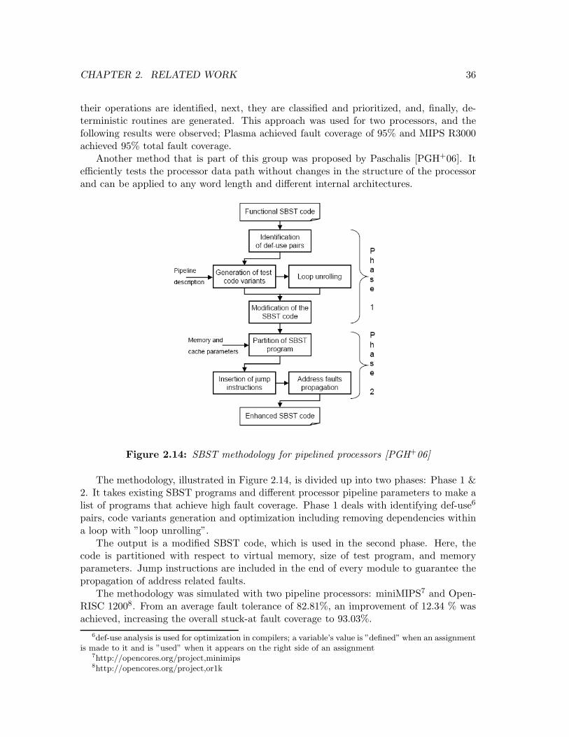
Another method that is part of this group was proposed by Paschalis [PGH+06]. Itefficiently tests the processor data path without changes in the structure of the processorand can be applied to any word length and different internal architectures.
Figure 2.14: SBST methodology for pipelined processors [PGH+06]
The methodology, illustrated in Figure 2.14, is divided up into two phases: Phase 1 &2. It takes existing SBST programs and different processor pipeline parameters to make alist of programs that achieve high fault coverage. Phase 1 deals with identifying def-use6
pairs, code variants generation and optimization including removing dependencies withina loop with ”loop unrolling”.
The output is a modified SBST code, which is used in the second phase. Here, thecode is partitioned with respect to virtual memory, size of test program, and memoryparameters. Jump instructions are included in the end of every module to guarantee thepropagation of address related faults.
The methodology was simulated with two pipeline processors: miniMIPS7 and Open-RISC 12008. From an average fault tolerance of 82.81%, an improvement of 12.34 % wasachieved, increasing the overall stuck-at fault coverage to 93.03%.
6def-use analysis is used for optimization in compilers; a variable’s value is ”defined” when an assignmentis made to it and is ”used” when it appears on the right side of an assignment
7http://opencores.org/project,minimips8http://opencores.org/project,or1k
CHAPTER 2. RELATED WORK 37
The method proposed by Chen [CWLG07] which generates test stimuli using the gatelevel of the processor description as entry point, is part of the ATPG Algorithms group .
The proposed method consists of multiple levels of abstraction, which are input tothe test development based on the information about the processor architecture, registertransfer-level and gate-level. To apply this method, the processor core must be subdividedinto different parts: ISA registers, IP Units, control, steering logic, pipeline registers, andhazard related logic.
After the classification, test routines are generated for every module. In the ISA Regis-ters, the development is focused on the structural faults of D Flip Flops. For the identifiedIPs, control & steering logic, and pipeline related logic, an ATPG tool generates the testpatterns focused on the ISA specification, RTL descriptions, and pipeline architecture ofthe target processor.
The methodology was tested in a processor core with an ARMv4 instruction set whichachieves a fault coverage of 93.74 % for stuck-at faults related to pipeline registers, ALU,Decoder, memory access unit etc.
Pseudo-random methods generate data together with testing instructions and let theprocessor perform the evaluation. Such a method is presented by a group of researchers[KLC+02]. It generates tests under the constraints of the ISA to avoid unwanted testpatterns. It is targeting structural faults like stuck-at and delay faults.
The method consists of two steps: test preparation and self-testing. Using a specialsoftware program, the tests which are generated are deliverable test patterns. The resultsare stored in the memory, and a selection is made using the constraints of the instructionset of the processor.
A component level fault simulation is performed to evaluate the test patterns. Afterevaluating the tests, evaluated they are tested on-chip.
Using this method, a test was performed on Parwan and DLX processors. For theParwan processor it took 5.3 instructions on average for a test vector with a fault coverageof 99.8%, while in the DLX processors 5.9 instructions with fault coverage of 96.3% forstuck-at and delay faults.
2.2.4 On-line Periodic Tests
Online periodic tests are performed during the normal operation of a processor. These testsreside in the RAM or Flash and are called by the operating system as normal programs.
Gizopoulos [PG04] proposed a SBST methodology to classify the processor componentsand characteristics of SBST test programs to be suitable for online periodic tests. Themethodology consists of three phases.
In the first phase, information is extracted from the ISA and the low register trans-fer level. The component operations are identified with specific input and outputs thatperform different operations, which includes multi-cycle data-paths or pipeline register.
In the second phase, different processor components are selected based on the sameproperties and component prioritization to generate test patterns, which will be trans-formed to a test routine.
CHAPTER 2. RELATED WORK 38
Based on how the different components are visible for the programmer, they can becharacterized as follows:
1. Visible components
2. Data-visible components
3. Address-visible components
4. Mixed (data & address) visible components
5. Partially visible components
6. Hidden components
Visible components are parts whose inputs and outputs are accessible from the assem-bler language programmers. Data-visible components are components like ALU, multipli-ers, dividers data registers etc. which serve as storage for input data test patterns. Theoutput data can be stored at register file, data memory, or both of them.
Address-visible components are components whose inputs and the outputs, receiveaddresses of the memory system. These appear in the instruction fetch unit or data-memory controller.
The mixed visible components use a mixed type of the inputs and outputs of thevisible and data visible components such as the adder used with the relative addressing.Partially visible components are the components which generate control signals and areimplemented as finite state machines. One such component is the processor control unitwhich affects the visible components. They have a medium testability.
The hidden components are architecture components which are included for perfor-mance and are not visible to assembly programming language. Such components arepipeline control units, branch prediction mechanisms etc.
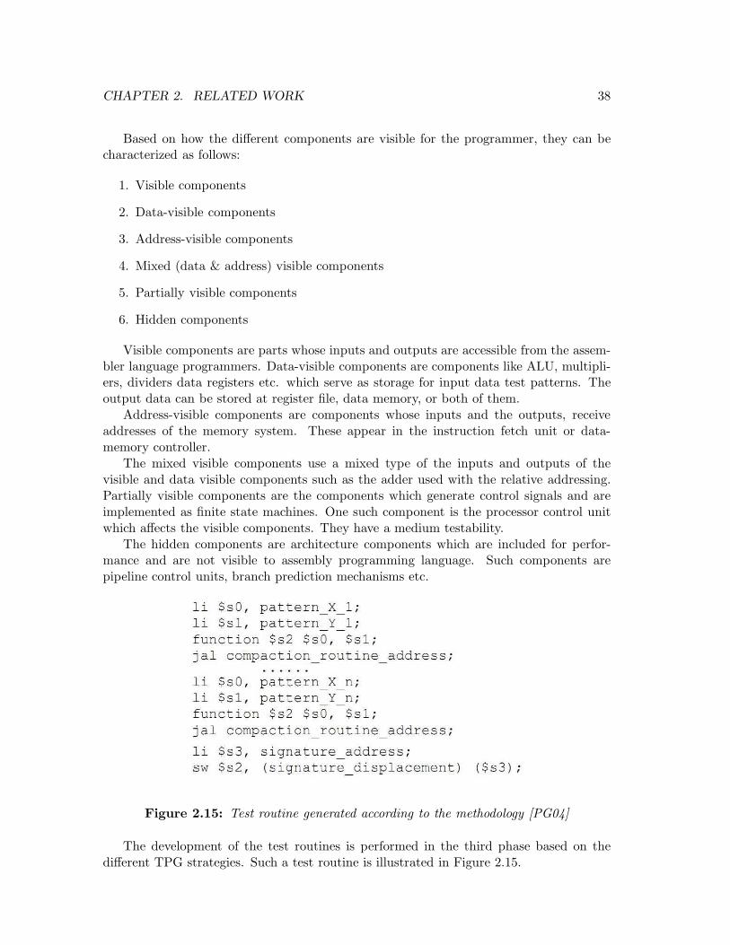
Figure 2.15: Test routine generated according to the methodology [PG04]
The development of the test routines is performed in the third phase based on thedifferent TPG strategies. Such a test routine is illustrated in Figure 2.15.
CHAPTER 2. RELATED WORK 39
A 32 bit RISC processor9 called Plasma was used to demonstrate the proposed method-ology, which achieves a fault coverage of 95.6 % for stuck at faults.
For the project SafetyLoan [TP07] several SBST tests were developed for an ARM7microcontroller. To test the RAM memory, the walking pattern algorithm is used. It isoptimized in a manner that read/write operations are performed in block segments of 32bytes, by a single command using multiple load and store. This reduces the number ofoperations to be performed in the RAM memory.
For the data integrity, cyclic redundancy checks with 16 bit are performed, whilefor register testing, the galloping pattern is used. The galloping pattern is described inSection 2.2.2.4.
The main problem with the register testing is that during the test runs, the values arestored in the memory. A possible solution to the problem is to swap the content betweenthe registers while the tests are running.
Testing the arithmetic logic unit is done by subdividing the instruction set into com-mand classes, which use the opcode as classifying parameter. The entire RAM was testedwithin 0.95 s, while ALU & register tests had a total execution time of 4.26 ms with ahigh diagnostic coverage.
2.2.5 Specialized Tests for Multi-cores
The research of last the years is going towards multi-core architectures for better per-formance and exploiting parallelism for instruction execution. These advances bring newchallenges for SBST techniques which must be adopted for multi-core architectures andcan be defined as [PGSR10]:
1. Use of SBST techniques that are proven for single core architectures to test all coresindividually
2. Speed up self testing routines with core and thread parallelism
3. Testing of interoperability logic at cores and threads levels
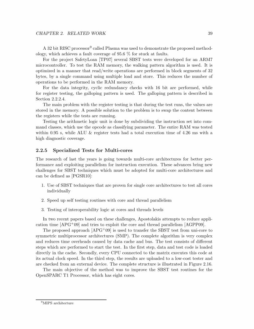
In two recent papers based on these challenges, Apostolakis attempts to reduce appli-cation time [APG+09] and tries to exploit the core and thread parallelism [AGPP09].
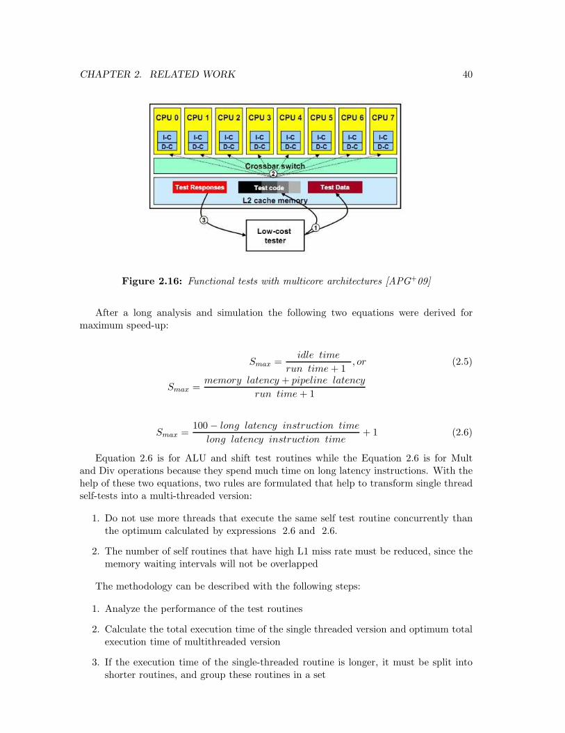
The proposed approach [APG+09] is used to transfer the SBST test from uni-core tosymmetric multiprocessor architectures (SMP). The complete algorithm is very complexand reduces time overheads caused by data cache and bus. The test consists of differentsteps which are performed to start the test. In the first step, data and test code is loadeddirectly in the cache. Secondly, every CPU connected to the matrix executes this code atits actual clock speed. In the third step, the results are uploaded to a low-cost tester andare checked from an external device. The complete structure is illustrated in Figure 2.16.
The main objective of the method was to improve the SBST test routines for theOpenSPARC T1 Processor, which has eight cores.
9MIPS architecture
CHAPTER 2. RELATED WORK 40
Figure 2.16: Functional tests with multicore architectures [APG+09]
After a long analysis and simulation the following two equations were derived formaximum speed-up:
Smax =idle time
run time+ 1, or (2.5)
Smax =memory latency + pipeline latency
run time+ 1
Smax =100− long latency instruction time
long latency instruction time+ 1 (2.6)
Equation 2.6 is for ALU and shift test routines while the Equation 2.6 is for Multand Div operations because they spend much time on long latency instructions. With thehelp of these two equations, two rules are formulated that help to transform single threadself-tests into a multi-threaded version:
1. Do not use more threads that execute the same self test routine concurrently thanthe optimum calculated by expressions 2.6 and 2.6.
2. The number of self routines that have high L1 miss rate must be reduced, since thememory waiting intervals will not be overlapped
The methodology can be described with the following steps:
1. Analyze the performance of the test routines
2. Calculate the total execution time of the single threaded version and optimum totalexecution time of multithreaded version
3. If the execution time of the single-threaded routine is longer, it must be split intoshorter routines, and group these routines in a set
CHAPTER 2. RELATED WORK 41
Figure 2.17: Performance results of multi-threaded over single-threaded [APG+09]
4. Select the longest routine from the set of self routines, assigns to it the smallestexecution time, which is the sum of all time single threaded routines assigned to thethread until now
• If this calculation contradicts one of two rules, give the routine the next shortestexecution time
• Remove this routine from the set
5. If the set is not empty, go to step 3, or exit.
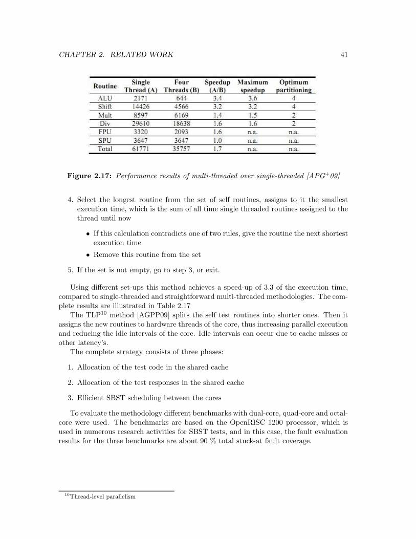
Using different set-ups this method achieves a speed-up of 3.3 of the execution time,compared to single-threaded and straightforward multi-threaded methodologies. The com-plete results are illustrated in Table 2.17
The TLP10 method [AGPP09] splits the self test routines into shorter ones. Then itassigns the new routines to hardware threads of the core, thus increasing parallel executionand reducing the idle intervals of the core. Idle intervals can occur due to cache misses orother latency’s.
The complete strategy consists of three phases:
1. Allocation of the test code in the shared cache
2. Allocation of the test responses in the shared cache
3. Efficient SBST scheduling between the cores
To evaluate the methodology different benchmarks with dual-core, quad-core and octal-core were used. The benchmarks are based on the OpenRISC 1200 processor, which isused in numerous research activities for SBST tests, and in this case, the fault evaluationresults for the three benchmarks are about 90 % total stuck-at fault coverage.
10Thread-level parallelism
Chapter 3
Analysis and Design
3.1 Evaluated Architectures
During the first steps of the thesis, different multi-core architectures were evaluated. Obvi-ously, there are many different multi-core microcontrollers which are intended to be usedin safety-related systems and many of them are designed to fulfil the IEC 61508 SIL-3certification criteria. But not all of them are suitable to be used in this area because theylack of safety features and are vulnerable to common cause failures.
According to the safety features, properties and the architectures, three microcon-trollers were chosen to be evaluated:
1. Texas Instruments TMS570
2. Infineon TC1766 (Audo-NextGeneration)
3. Toshiba/Yogitech fRMethodology (Fault Robust Methodology)
In the Sections 2.1.2 and 2.1.3 different controller strategies are discussed, and a shortdescription about possible implementations is given. Now, architectures are examinedfrom the industrial perspective to see how these concepts are used in practice. In thefollowing, the three architectures are described.
3.1.1 TMS570 - Texas Instruments
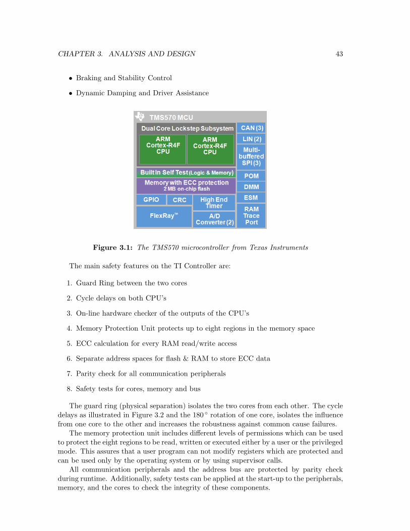
Referring to Figure 3.1, the controller has two cores connected in Lock - Step Mode1. Ituses two ARM R© Cortex-R4F cores, with floating point unit to meet the SIL-3/ASIL-Dlevel according to the IEC-61508 and ISO-26262.
Target applications for the microcontroller are:
• Electronic Power Steering
• Active Steering
• Integrated Chassis Management
1Described in Page 21 with Figure 2.7a
42
CHAPTER 3. ANALYSIS AND DESIGN 43
• Braking and Stability Control
• Dynamic Damping and Driver Assistance
Figure 3.1: The TMS570 microcontroller from Texas Instruments
The main safety features on the TI Controller are:
1. Guard Ring between the two cores
2. Cycle delays on both CPU’s
3. On-line hardware checker of the outputs of the CPU’s
4. Memory Protection Unit protects up to eight regions in the memory space
5. ECC calculation for every RAM read/write access
6. Separate address spaces for flash & RAM to store ECC data
7. Parity check for all communication peripherals
8. Safety tests for cores, memory and bus
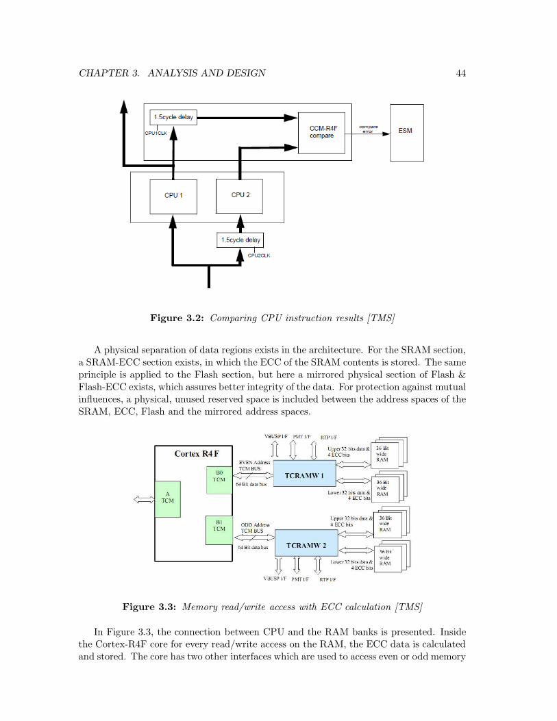
The guard ring (physical separation) isolates the two cores from each other. The cycledelays as illustrated in Figure 3.2 and the 180 ◦ rotation of one core, isolates the influencefrom one core to the other and increases the robustness against common cause failures.
The memory protection unit includes different levels of permissions which can be usedto protect the eight regions to be read, written or executed either by a user or the privilegedmode. This assures that a user program can not modify registers which are protected andcan be used only by the operating system or by using supervisor calls.
All communication peripherals and the address bus are protected by parity checkduring runtime. Additionally, safety tests can be applied at the start-up to the peripherals,memory, and the cores to check the integrity of these components.
CHAPTER 3. ANALYSIS AND DESIGN 44
Figure 3.2: Comparing CPU instruction results [TMS]
A physical separation of data regions exists in the architecture. For the SRAM section,a SRAM-ECC section exists, in which the ECC of the SRAM contents is stored. The sameprinciple is applied to the Flash section, but here a mirrored physical section of Flash &Flash-ECC exists, which assures better integrity of the data. For protection against mutualinfluences, a physical, unused reserved space is included between the address spaces of theSRAM, ECC, Flash and the mirrored address spaces.
Figure 3.3: Memory read/write access with ECC calculation [TMS]
In Figure 3.3, the connection between CPU and the RAM banks is presented. Insidethe Cortex-R4F core for every read/write access on the RAM, the ECC data is calculatedand stored. The core has two other interfaces which are used to access even or odd memory
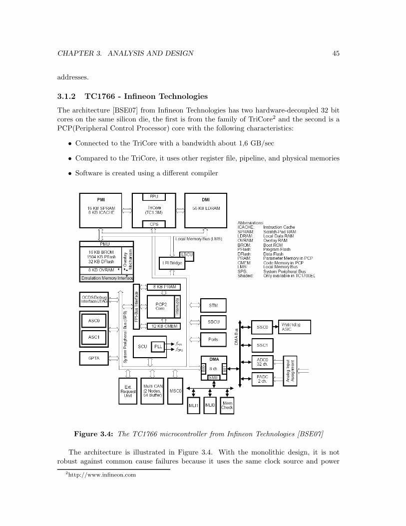
CHAPTER 3. ANALYSIS AND DESIGN 45
addresses.
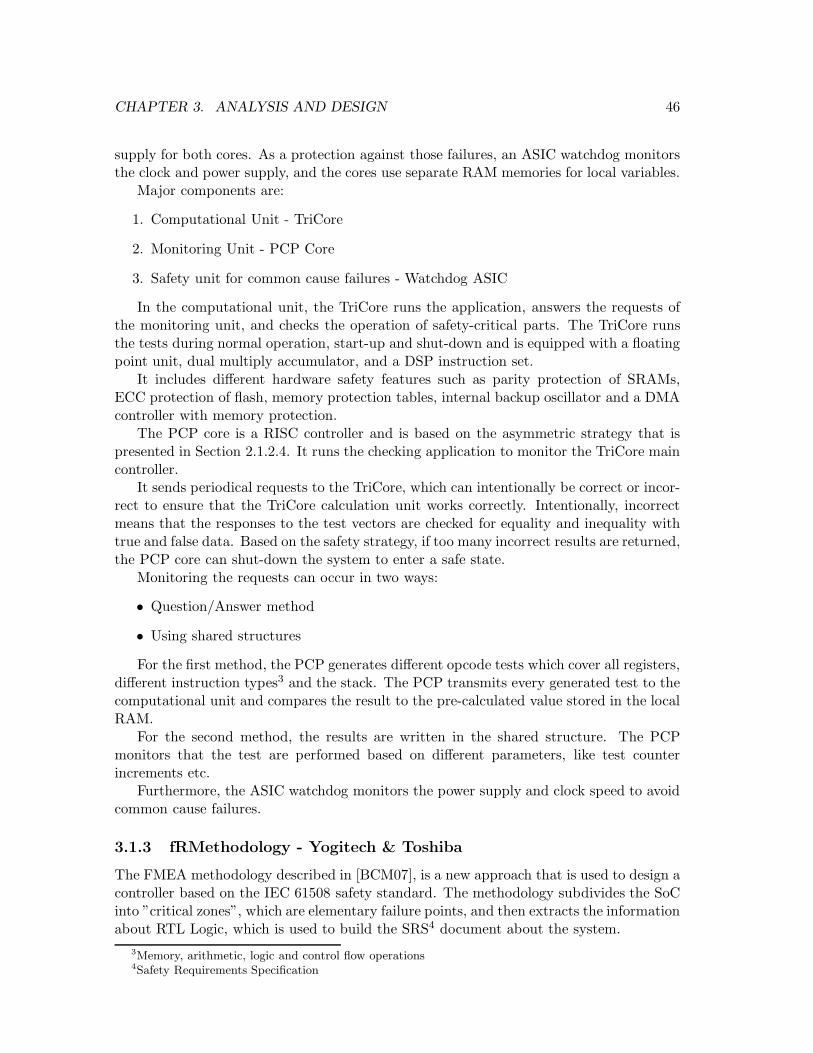
3.1.2 TC1766 - Infineon Technologies
The architecture [BSE07] from Infineon Technologies has two hardware-decoupled 32 bitcores on the same silicon die, the first is from the family of TriCore2 and the second is aPCP(Peripheral Control Processor) core with the following characteristics:
• Connected to the TriCore with a bandwidth about 1,6 GB/sec
• Compared to the TriCore, it uses other register file, pipeline, and physical memories
• Software is created using a different compiler
Figure 3.4: The TC1766 microcontroller from Infineon Technologies [BSE07]
The architecture is illustrated in Figure 3.4. With the monolithic design, it is notrobust against common cause failures because it uses the same clock source and power
2http://www.infineon.com
CHAPTER 3. ANALYSIS AND DESIGN 46
supply for both cores. As a protection against those failures, an ASIC watchdog monitorsthe clock and power supply, and the cores use separate RAM memories for local variables.
Major components are:
1. Computational Unit - TriCore
2. Monitoring Unit - PCP Core
3. Safety unit for common cause failures - Watchdog ASIC
In the computational unit, the TriCore runs the application, answers the requests ofthe monitoring unit, and checks the operation of safety-critical parts. The TriCore runsthe tests during normal operation, start-up and shut-down and is equipped with a floatingpoint unit, dual multiply accumulator, and a DSP instruction set.
It includes different hardware safety features such as parity protection of SRAMs,ECC protection of flash, memory protection tables, internal backup oscillator and a DMAcontroller with memory protection.
The PCP core is a RISC controller and is based on the asymmetric strategy that ispresented in Section 2.1.2.4. It runs the checking application to monitor the TriCore maincontroller.
It sends periodical requests to the TriCore, which can intentionally be correct or incor-rect to ensure that the TriCore calculation unit works correctly. Intentionally, incorrectmeans that the responses to the test vectors are checked for equality and inequality withtrue and false data. Based on the safety strategy, if too many incorrect results are returned,the PCP core can shut-down the system to enter a safe state.
Monitoring the requests can occur in two ways:
• Question/Answer method
• Using shared structures
For the first method, the PCP generates different opcode tests which cover all registers,different instruction types3 and the stack. The PCP transmits every generated test to thecomputational unit and compares the result to the pre-calculated value stored in the localRAM.
For the second method, the results are written in the shared structure. The PCPmonitors that the test are performed based on different parameters, like test counterincrements etc.
Furthermore, the ASIC watchdog monitors the power supply and clock speed to avoidcommon cause failures.
3.1.3 fRMethodology - Yogitech & Toshiba
The FMEA methodology described in [BCM07], is a new approach that is used to design acontroller based on the IEC 61508 safety standard. The methodology subdivides the SoCinto ”critical zones”, which are elementary failure points, and then extracts the informationabout RTL Logic, which is used to build the SRS4 document about the system.
3Memory, arithmetic, logic and control flow operations4Safety Requirements Specification
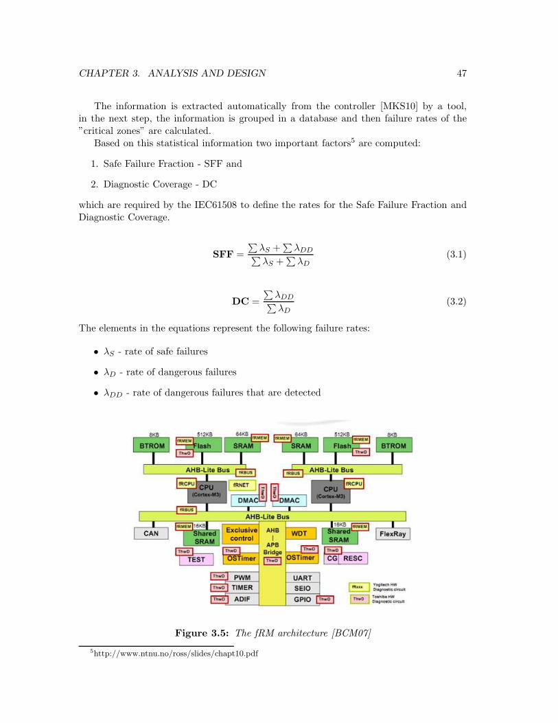
CHAPTER 3. ANALYSIS AND DESIGN 47
The information is extracted automatically from the controller [MKS10] by a tool,in the next step, the information is grouped in a database and then failure rates of the”critical zones” are calculated.
Based on this statistical information two important factors5 are computed:
1. Safe Failure Fraction - SFF and
2. Diagnostic Coverage - DC
which are required by the IEC61508 to define the rates for the Safe Failure Fraction andDiagnostic Coverage.
SFF =
∑λS +
∑λDD
∑λS +
∑λD
(3.1)
DC =
∑λDD
∑λD
(3.2)
The elements in the equations represent the following failure rates:
• λS - rate of safe failures
• λD - rate of dangerous failures
• λDD - rate of dangerous failures that are detected
Figure 3.5: The fRM architecture [BCM07]
5http://www.ntnu.no/ross/slides/chapt10.pdf
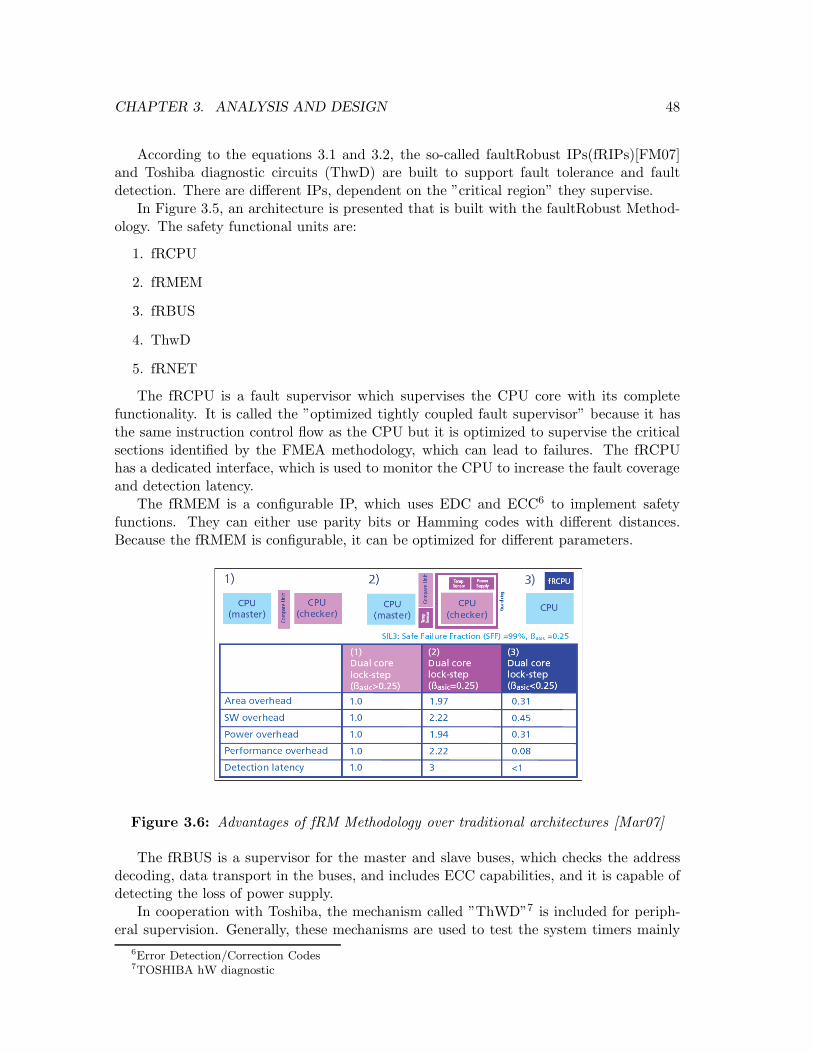
CHAPTER 3. ANALYSIS AND DESIGN 48
According to the equations 3.1 and 3.2, the so-called faultRobust IPs(fRIPs)[FM07]and Toshiba diagnostic circuits (ThwD) are built to support fault tolerance and faultdetection. There are different IPs, dependent on the ”critical region” they supervise.
In Figure 3.5, an architecture is presented that is built with the faultRobust Method-ology. The safety functional units are:
1. fRCPU
2. fRMEM
3. fRBUS
4. ThwD
5. fRNET
The fRCPU is a fault supervisor which supervises the CPU core with its completefunctionality. It is called the ”optimized tightly coupled fault supervisor” because it hasthe same instruction control flow as the CPU but it is optimized to supervise the criticalsections identified by the FMEA methodology, which can lead to failures. The fRCPUhas a dedicated interface, which is used to monitor the CPU to increase the fault coverageand detection latency.
The fRMEM is a configurable IP, which uses EDC and ECC6 to implement safetyfunctions. They can either use parity bits or Hamming codes with different distances.Because the fRMEM is configurable, it can be optimized for different parameters.
Figure 3.6: Advantages of fRM Methodology over traditional architectures [Mar07]
The fRBUS is a supervisor for the master and slave buses, which checks the addressdecoding, data transport in the buses, and includes ECC capabilities, and it is capable ofdetecting the loss of power supply.
In cooperation with Toshiba, the mechanism called ”ThWD”7 is included for periph-eral supervision. Generally, these mechanisms are used to test the system timers mainly
6Error Detection/Correction Codes7TOSHIBA hW diagnostic
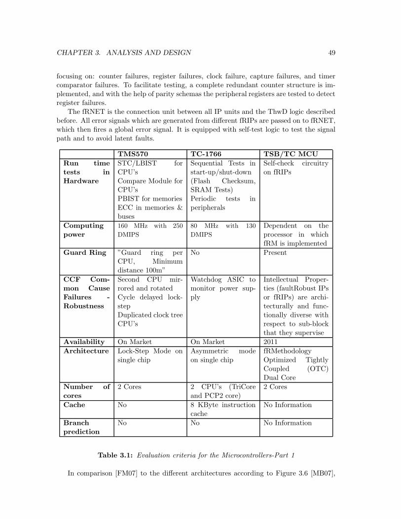
CHAPTER 3. ANALYSIS AND DESIGN 49
focusing on: counter failures, register failures, clock failure, capture failures, and timercomparator failures. To facilitate testing, a complete redundant counter structure is im-plemented, and with the help of parity schemas the peripheral registers are tested to detectregister failures.
The fRNET is the connection unit between all IP units and the ThwD logic describedbefore. All error signals which are generated from different fRIPs are passed on to fRNET,which then fires a global error signal. It is equipped with self-test logic to test the signalpath and to avoid latent faults.
TMS570 TC-1766 TSB/TC MCU
Run timetests inHardware
STC/LBIST forCPU’sCompare Module forCPU’sPBIST for memoriesECC in memories &buses
Sequential Tests instart-up/shut-down(Flash Checksum,SRAM Tests)Periodic tests inperipherals
Self-check circuitryon fRIPs
Computingpower
160 MHz with 250
DMIPS
80 MHz with 130
DMIPS
Dependent on theprocessor in whichfRM is implemented
Guard Ring ”Guard ring perCPU, Minimumdistance 100m”
No Present
CCF Com-mon CauseFailures -Robustness
Second CPU mir-rored and rotatedCycle delayed lock-stepDuplicated clock treeCPU’s
Watchdog ASIC tomonitor power sup-ply
Intellectual Proper-ties (faultRobust IPsor fRIPs) are archi-tecturally and func-tionally diverse withrespect to sub-blockthat they supervise
Availability On Market On Market 2011
Architecture Lock-Step Mode onsingle chip
Asymmetric modeon single chip
fRMethodologyOptimized TightlyCoupled (OTC)Dual Core
Number ofcores
2 Cores 2 CPU’s (TriCoreand PCP2 core)
2 Cores
Cache No 8 KByte instructioncache
No Information
Branchprediction
No No No Information
Table 3.1: Evaluation criteria for the Microcontrollers-Part 1
In comparison [FM07] to the different architectures according to Figure 3.6 [MB07],
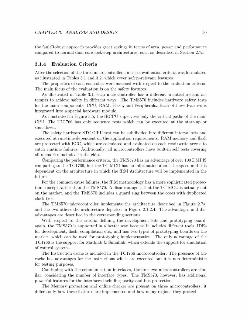
CHAPTER 3. ANALYSIS AND DESIGN 50
the faultRobust approach provides great savings in terms of area, power and performancecompared to normal dual core lock-step architectures, such as described in Section 2.7a.
3.1.4 Evaluation Criteria
After the selection of the three microcontrollers, a list of evaluation criteria was formulatedas illustrated in Tables 3.1 and 3.2, which cover safety-relevant features.
The properties of each controller were assessed with respect to the evaluation criteria.The main focus of the evaluation is on the safety features.
As illustrated in Table 3.1, each microcontroller has a different architecture and at-tempts to achieve safety in different ways. The TMS570 includes hardware safety testsfor the main components: CPU, RAM, Flash, and Peripherals. Each of these features isintegrated into a special hardware module.
As illustrated in Figure 3.5, the fRCPU supervises only the critical paths of the mainCPU. The TC1766 has only sequence tests which can be executed at the start-up orshut-down.
The safety hardware STC/CPU test can be subdivided into different interval sets andexecuted at run-time dependent on the application requirements. RAM memory and flashare protected with ECC, which are calculated and evaluated on each read/write access tocatch runtime failures. Additionally, all microcontrollers have built-in self tests coveringall memories included in the chip.
Comparing the performance criteria, the TMS570 has an advantage of over 100 DMPIScomparing to the TC1766, but the TC MCU has no information about the speed and it isdependent on the architecture in which the fRM Architecture will be implemented in thefuture.
For the common cause failures, the fRM methodology has a more sophisticated protec-tion concept rather than the TMS570. A disadvantage is that the TC-MCU is actually noton the market, and the TMS570 includes a guard ring between the cores with duplicatedclock tree.
The TMS570 microcontroller implements the architecture described in Figure 2.7a,and the two others the architecture depicted in Figure 2.1.2.4. The advantages and dis-advantages are described in the corresponding sections.
With respect to the criteria defining the development kits and prototyping board,again, the TMS570 is supported in a better way because it includes different tools, IDEsfor development, flash, compilation etc., and has two types of prototyping boards on themarket, which can be used for prototyping implementation. The only advantage of theTC1766 is the support for Mathlab & Simulink, which extends the support for simulationof control systems.
The Instruction cache is included in the TC1766 microcontroller. The presence of thecache has advantages for the instructions which are executed but it is non deterministicfor testing purposes.
Continuing with the communication interfaces, the first two microcontrollers are sim-ilar, considering the number of interface types. The TMS570, however, has additionalpowerful features for the interfaces including parity and bus protection.
The Memory protection and online checker are present on three microcontrollers, itdiffers only how these features are implemented and how many regions they protect.
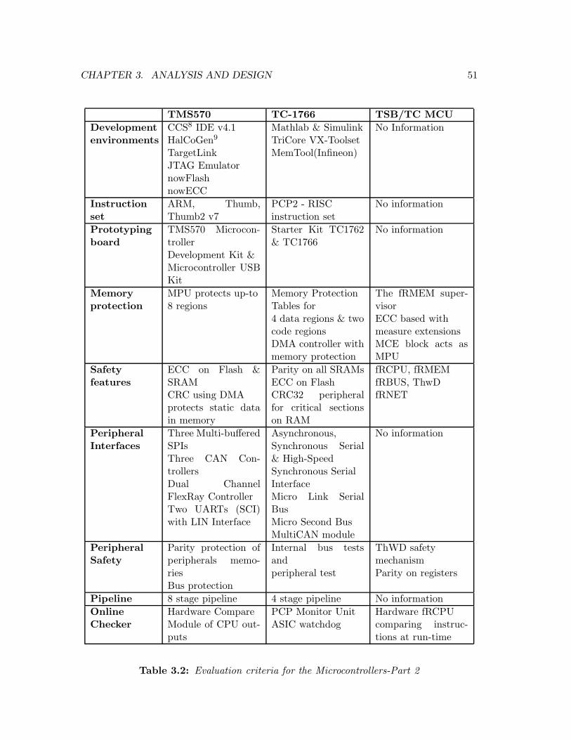
CHAPTER 3. ANALYSIS AND DESIGN 51
TMS570 TC-1766 TSB/TC MCU
Developmentenvironments
CCS8 IDE v4.1HalCoGen9
TargetLinkJTAG EmulatornowFlashnowECC
Mathlab & SimulinkTriCore VX-ToolsetMemTool(Infineon)
No Information
Instructionset
ARM, Thumb,Thumb2 v7
PCP2 - RISCinstruction set
No information
Prototypingboard
TMS570 Microcon-trollerDevelopment Kit &Microcontroller USBKit
Starter Kit TC1762& TC1766
No information
Memoryprotection
MPU protects up-to8 regions
Memory ProtectionTables for4 data regions & twocode regionsDMA controller withmemory protection
The fRMEM super-visorECC based withmeasure extensionsMCE block acts asMPU
Safetyfeatures
ECC on Flash &SRAMCRC using DMAprotects static datain memory
Parity on all SRAMsECC on FlashCRC32 peripheralfor critical sectionson RAM
fRCPU, fRMEMfRBUS, ThwDfRNET
PeripheralInterfaces
Three Multi-bufferedSPIsThree CAN Con-trollersDual ChannelFlexRay ControllerTwo UARTs (SCI)with LIN Interface
Asynchronous,Synchronous Serial& High-SpeedSynchronous SerialInterfaceMicro Link SerialBusMicro Second BusMultiCAN module
No information
PeripheralSafety
Parity protection ofperipherals memo-riesBus protection
Internal bus testsandperipheral test
ThWD safetymechanismParity on registers
Pipeline 8 stage pipeline 4 stage pipeline No information
OnlineChecker
Hardware CompareModule of CPU out-puts
PCP Monitor UnitASIC watchdog
Hardware fRCPUcomparing instruc-tions at run-time
Table 3.2: Evaluation criteria for the Microcontrollers-Part 2
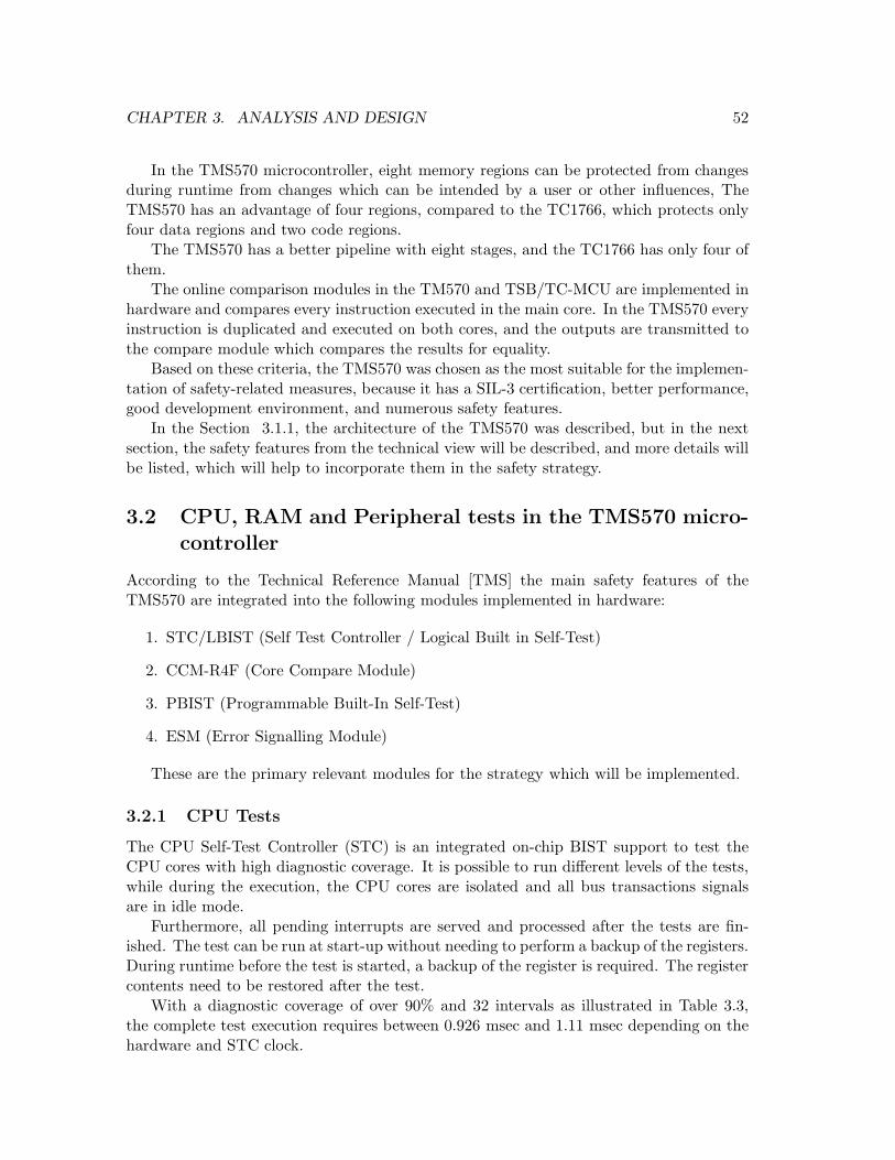
CHAPTER 3. ANALYSIS AND DESIGN 52
In the TMS570 microcontroller, eight memory regions can be protected from changesduring runtime from changes which can be intended by a user or other influences, TheTMS570 has an advantage of four regions, compared to the TC1766, which protects onlyfour data regions and two code regions.
The TMS570 has a better pipeline with eight stages, and the TC1766 has only four ofthem.
The online comparison modules in the TM570 and TSB/TC-MCU are implemented inhardware and compares every instruction executed in the main core. In the TMS570 everyinstruction is duplicated and executed on both cores, and the outputs are transmitted tothe compare module which compares the results for equality.
Based on these criteria, the TMS570 was chosen as the most suitable for the implemen-tation of safety-related measures, because it has a SIL-3 certification, better performance,good development environment, and numerous safety features.
In the Section 3.1.1, the architecture of the TMS570 was described, but in the nextsection, the safety features from the technical view will be described, and more details willbe listed, which will help to incorporate them in the safety strategy.
3.2 CPU, RAM and Peripheral tests in the TMS570 micro-
controller
According to the Technical Reference Manual [TMS] the main safety features of theTMS570 are integrated into the following modules implemented in hardware:
1. STC/LBIST (Self Test Controller / Logical Built in Self-Test)
2. CCM-R4F (Core Compare Module)
3. PBIST (Programmable Built-In Self-Test)
4. ESM (Error Signalling Module)
These are the primary relevant modules for the strategy which will be implemented.
3.2.1 CPU Tests
The CPU Self-Test Controller (STC) is an integrated on-chip BIST support to test theCPU cores with high diagnostic coverage. It is possible to run different levels of the tests,while during the execution, the CPU cores are isolated and all bus transactions signalsare in idle mode.
Furthermore, all pending interrupts are served and processed after the tests are fin-ished. The test can be run at start-up without needing to perform a backup of the registers.During runtime before the test is started, a backup of the register is required. The registercontents need to be restored after the test.
With a diagnostic coverage of over 90% and 32 intervals as illustrated in Table 3.3,the complete test execution requires between 0.926 msec and 1.11 msec depending on thehardware and STC clock.
CHAPTER 3. ANALYSIS AND DESIGN 53
Intervals Test Coverage [%] Test Cycle
0 0 0
1 57,14 1555
2 65,82 3108
. . .
. . .
15 86,19 23297
16 86,56 24850
17 86,97 26403
. . .
. . .
30 90,46 46592
31 90,64 48145
32 90,84 49698
Table 3.3: STC levels and coverage [TMS]
3.2.2 Core Compare Module Tests
The core compare module not only is responsible to compare the results of the outputinstructions, it also contains the following built in self tests which can be used duringruntime:
• self-test
• error forcing test
• self-test error forcing mode
The start of the test must be issued by the application. During the ”self test”, themodule can generate compare match and compare mismatch patterns. Applying comparematch patterns (four patters 0x0, 0x1, 0xA, 0x5) at the outputs, equal results are expected.If a fault is detected, an ESM error is generated, and the test is terminated, otherwise thetermination must be performed by the application.
The compare mismatch patterns are applied in the same manner with the differencethat the patterns for the second core are inverted, and different result is expected as inthe first core. The test takes 3615 test cycles.
Applying the error forcing test only one pattern is applied to force that an error isintroduced in path between CCMR4F and ESM. If after the test is applied, and no erroris asserted on the ESM module, a hardware fault is present.
The tests that are described check only the CCMR4F module, and the normal applica-tion can use the CPU’s in the background, but the outputs of the CPU’s are not comparedwith each other.
CHAPTER 3. ANALYSIS AND DESIGN 54
3.2.3 RAM and Peripheral Tests
The PBIST (Programmable Built-In Self Test) architecture is a built-in testing enginecontrolled by a small CPU. It offers the possibility to test all types of memories withpre-implemented algorithms in the microcontroller.
Ram Group Module Memory type
3 DCAN1 Single Port
4 DCAN2 Single Port
5 DCAN3 Single Port
6 ESRAM Single Port
7 MIBSPI Single Port
8 VIM Single Port
9 MibADC Two Port
10 DMA Two Port
11 NHET Two Port
12 HET TU Two Port
13 RTP Two Port
14 Flexray Single Port
Table 3.4: RAM groups in TMS570 [TMS]
In Table 3.4, all RAM memories with types of the microcontroller are presented. Foreach type of memory, in Table 3.5 the algorithms are shown.
Memorytype
Module Valid RAM Groups
Single Port march13n-red 3,4,5,6,7,8,14
Two Port march13n-red 9,10,11,12,13
Single Port down1A-red 3,4,5,6,7,8,14
Two Port down1A-red 9,10,11,12,13
Single Port mapcolumn 3,4,5,6,7,8,14
Two Port mapcolumn 9,10,11,12,13
Single Port precharge 3,4,5,6,7,8,14
Two Port precharge 9,10,11,12,13
Single Port dtxn2 3,4,5,6,7,8,14
Two Port dtxn2 9,10,11,12,13
Table 3.5: Algorithm to RAM mapping in TMS570 [TMS]
• March13N - As described in Section 2.2.2.2, March13N provides very high diagnosticcoverage. The fault types detected by this algorithm are manifold starting from,decoder, stuck-at, coupled, parametric faults, and ending with logic faults. With13N operations where N is number of RAM Cells, it has linear complexity O(n).
CHAPTER 3. ANALYSIS AND DESIGN 55
• Map Column - is commonly used to find bit lines sensitivities in memory. It consistsof writing on each line of memory 1 and 0’s and repeatedly reading and writing back.
• Pre-Charge - used to address the pre-charging of the SRAM cells because the analogportion is frequency-sensitive.
• DOWN1a - addresses the data bits and address bits by switching their content witha forced transition.
• DTXN2a - mainly used to test decoding logic in RAM memories.
The complete content of the affected memory part are lost after the tests are applied.Therefore, all these tests are carried out at the start-up. The complete tests needs 23.23msec at HCLK = 80 MHz and ROMCLK = 100 MHz and 43.63 msec with HCLK = 100MHz and ROMCLK = 40 MHz to be completely executed.
3.2.4 Error Signaling Module - ESM
The ESM Module is used to control the error signals that come from different sources ofthe microcontroller and can be transmitted to a dedicated external pin.
The main properties of the ESM module are :
• 96 interrupt/error channels for various error sources
• Dedicated pin ERROR to signal external sources
The first thirty two error sources are maskable during normal runtime, and the restare non-maskable.
3.3 Functional Safety Requirements
• At start-up, the RAM should be initialized with ECC.
• At start-up,all RAM memories must be tested with the PBIST logic, which ensuresthat the RAM and Peripheral memories are in a safe state.
• The RAM must be initialized to a known state.
• It must be ensured that all errors are reported correctly and that the system doesnot enter an unsafe state.
• During runtime the RAM must be tested completely, and it must be guaranteed thatthe normal application software is not halted in its normal operation.
• It must be ensured that after disabling the Interrupts, they are enabled after thetest is finished.
• During runtime the execution time of the RAM test must not exceed the criticaltime for which the Interrupts are disabled.
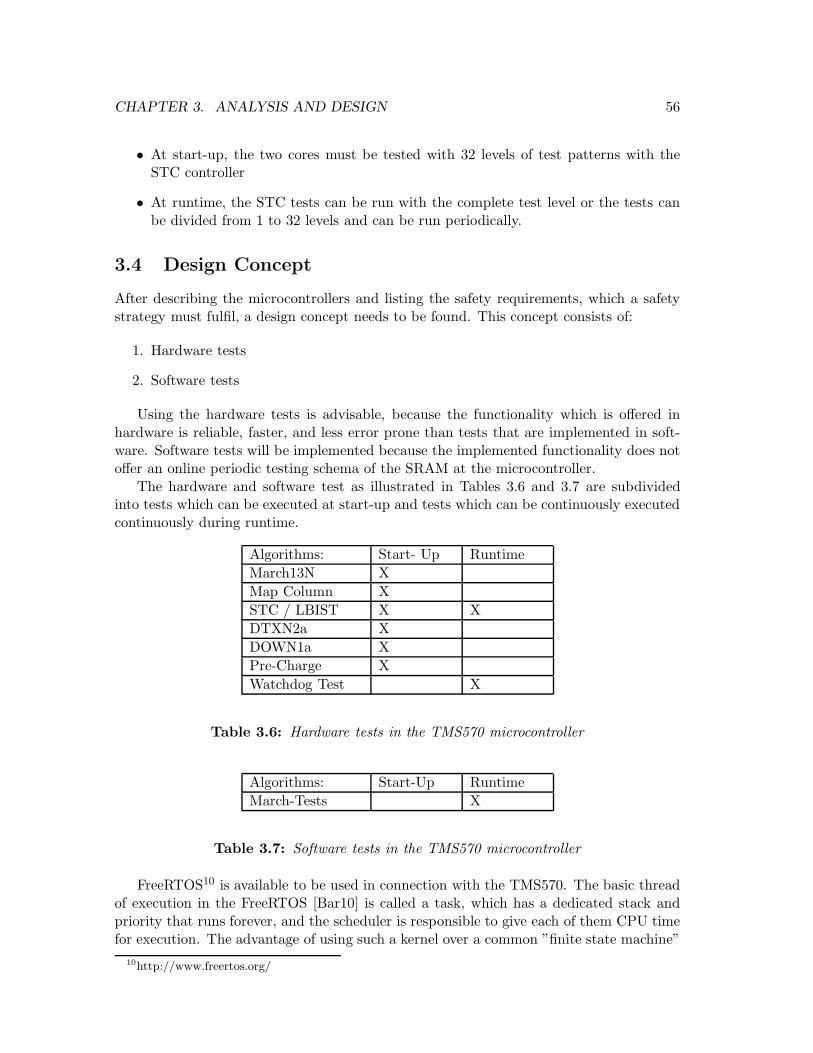
CHAPTER 3. ANALYSIS AND DESIGN 56
• At start-up, the two cores must be tested with 32 levels of test patterns with theSTC controller
• At runtime, the STC tests can be run with the complete test level or the tests canbe divided from 1 to 32 levels and can be run periodically.
3.4 Design Concept
After describing the microcontrollers and listing the safety requirements, which a safetystrategy must fulfil, a design concept needs to be found. This concept consists of:
1. Hardware tests
2. Software tests
Using the hardware tests is advisable, because the functionality which is offered inhardware is reliable, faster, and less error prone than tests that are implemented in soft-ware. Software tests will be implemented because the implemented functionality does notoffer an online periodic testing schema of the SRAM at the microcontroller.
The hardware and software test as illustrated in Tables 3.6 and 3.7 are subdividedinto tests which can be executed at start-up and tests which can be continuously executedcontinuously during runtime.
Algorithms: Start- Up Runtime
March13N X
Map Column X
STC / LBIST X X
DTXN2a X
DOWN1a X
Pre-Charge X
Watchdog Test X
Table 3.6: Hardware tests in the TMS570 microcontroller
Algorithms: Start-Up Runtime
March-Tests X
Table 3.7: Software tests in the TMS570 microcontroller
FreeRTOS10 is available to be used in connection with the TMS570. The basic threadof execution in the FreeRTOS [Bar10] is called a task, which has a dedicated stack andpriority that runs forever, and the scheduler is responsible to give each of them CPU timefor execution. The advantage of using such a kernel over a common ”finite state machine”
10http://www.freertos.org/
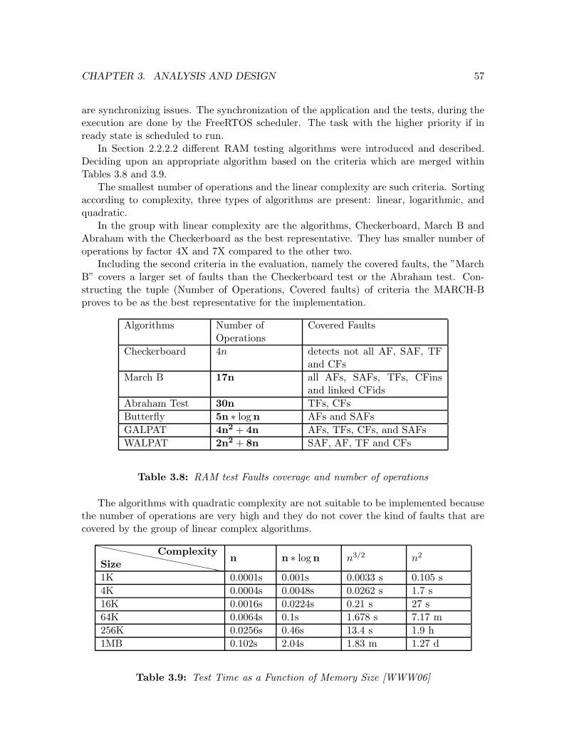
CHAPTER 3. ANALYSIS AND DESIGN 57
are synchronizing issues. The synchronization of the application and the tests, during theexecution are done by the FreeRTOS scheduler. The task with the higher priority if inready state is scheduled to run.
In Section 2.2.2.2 different RAM testing algorithms were introduced and described.Deciding upon an appropriate algorithm based on the criteria which are merged withinTables 3.8 and 3.9.
The smallest number of operations and the linear complexity are such criteria. Sortingaccording to complexity, three types of algorithms are present: linear, logarithmic, andquadratic.
In the group with linear complexity are the algorithms, Checkerboard, March B andAbraham with the Checkerboard as the best representative. They has smaller number ofoperations by factor 4X and 7X compared to the other two.
Including the second criteria in the evaluation, namely the covered faults, the ”MarchB” covers a larger set of faults than the Checkerboard test or the Abraham test. Con-structing the tuple (Number of Operations, Covered faults) of criteria the MARCH-Bproves to be as the best representative for the implementation.
Algorithms Number ofOperations
Covered Faults
Checkerboard 4n detects not all AF, SAF, TFand CFs
March B 17n all AFs, SAFs, TFs, CFinsand linked CFids
Abraham Test 30n TFs, CFs
Butterfly 5n ∗ log n AFs and SAFs
GALPAT 4n2 + 4n AFs, TFs, CFs, and SAFs
WALPAT 2n2 + 8n SAF, AF, TF and CFs
Table 3.8: RAM test Faults coverage and number of operations
The algorithms with quadratic complexity are not suitable to be implemented becausethe number of operations are very high and they do not cover the kind of faults that arecovered by the group of linear complex algorithms.
``````````````
SizeComplexity
n n ∗ logn n3/2 n2
1K 0.0001s 0.001s 0.0033 s 0.105 s
4K 0.0004s 0.0048s 0.0262 s 1.7 s
16K 0.0016s 0.0224s 0.21 s 27 s
64K 0.0064s 0.1s 1.678 s 7.17 m
256K 0.0256s 0.46s 13.4 s 1.9 h
1MB 0.102s 2.04s 1.83 m 1.27 d
Table 3.9: Test Time as a Function of Memory Size [WWW06]
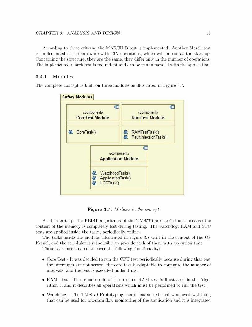
CHAPTER 3. ANALYSIS AND DESIGN 58
According to these criteria, the MARCH B test is implemented. Another March testis implemented in the hardware with 13N operations, which will be run at the start-up.Concerning the structure, they are the same, they differ only in the number of operations.The implemented march test is redundant and can be run in parallel with the application.
3.4.1 Modules
The complete concept is built on three modules as illustrated in Figure 3.7.
Figure 3.7: Modules in the concept
At the start-up, the PBIST algorithms of the TMS570 are carried out, because thecontent of the memory is completely lost during testing. The watchdog, RAM and STCtests are applied inside the tasks, periodically online.
The tasks inside the modules illustrated in Figure 3.8 exist in the context of the OSKernel, and the scheduler is responsible to provide each of them with execution time.
These tasks are created to cover the following functionality:
• Core Test - It was decided to run the CPU test periodically because during that testthe interrupts are not served, the core test is adaptable to configure the number ofintervals, and the test is executed under 1 ms.
• RAM Test - The pseudo-code of the selected RAM test is illustrated in the Algo-rithm 5, and it describes all operations which must be performed to run the test.
• Watchdog - The TMS570 Prototyping board has an external windowed watchdogthat can be used for program flow monitoring of the application and it is integrated
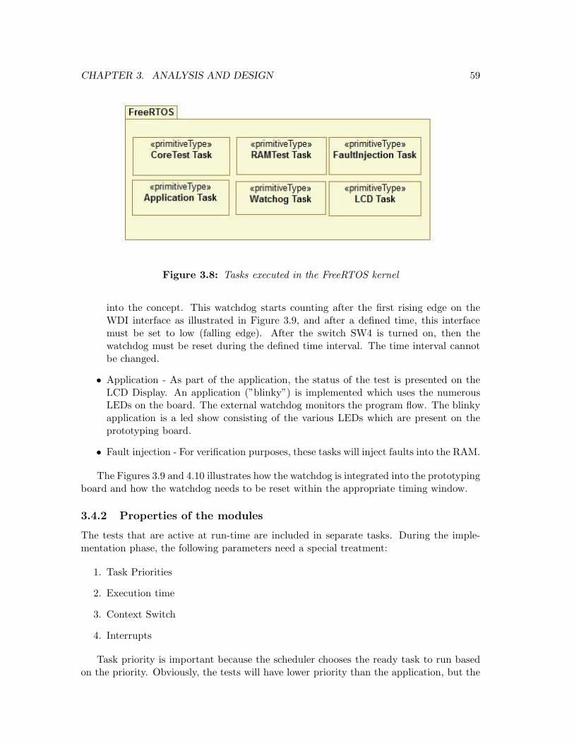
CHAPTER 3. ANALYSIS AND DESIGN 59
Figure 3.8: Tasks executed in the FreeRTOS kernel
into the concept. This watchdog starts counting after the first rising edge on theWDI interface as illustrated in Figure 3.9, and after a defined time, this interfacemust be set to low (falling edge). After the switch SW4 is turned on, then thewatchdog must be reset during the defined time interval. The time interval cannotbe changed.
• Application - As part of the application, the status of the test is presented on theLCD Display. An application (”blinky”) is implemented which uses the numerousLEDs on the board. The external watchdog monitors the program flow. The blinkyapplication is a led show consisting of the various LEDs which are present on theprototyping board.
• Fault injection - For verification purposes, these tasks will inject faults into the RAM.
The Figures 3.9 and 4.10 illustrates how the watchdog is integrated into the prototypingboard and how the watchdog needs to be reset within the appropriate timing window.
3.4.2 Properties of the modules
The tests that are active at run-time are included in separate tasks. During the imple-mentation phase, the following parameters need a special treatment:
1. Task Priorities
2. Execution time
3. Context Switch
4. Interrupts
Task priority is important because the scheduler chooses the ready task to run basedon the priority. Obviously, the tests will have lower priority than the application, but the
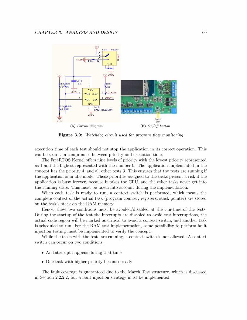
CHAPTER 3. ANALYSIS AND DESIGN 60
(a) Circuit diagram (b) On/off button
Figure 3.9: Watchdog circuit used for program flow monitoring
execution time of each test should not stop the application in its correct operation. Thiscan be seen as a compromise between priority and execution time.
The FreeRTOS Kernel offers nine levels of priority with the lowest priority representedas 1 and the highest represented with the number 9. The application implemented in theconcept has the priority 4, and all other tests 3. This ensures that the tests are running ifthe application is in idle mode. These priorities assigned to the tasks present a risk if theapplication is busy forever, because it takes the CPU, and the other tasks never get intothe running state. This must be taken into account during the implementation.
When each task is ready to run, a context switch is performed, which means thecomplete context of the actual task (program counter, registers, stack pointer) are storedon the task’s stack on the RAM memory.
Hence, these two conditions must be avoided/disabled at the run-time of the tests.During the startup of the test the interrupts are disabled to avoid test interruptions, theactual code region will be marked as critical to avoid a context switch, and another taskis scheduled to run. For the RAM test implementation, some possibility to perform faultinjection testing must be implemented to verify the concept.
While the tasks with the tests are running, a context switch is not allowed. A contextswitch can occur on two conditions:
• An Interrupt happens during that time
• One task with higher priority becomes ready
The fault coverage is guaranteed due to the March Test structure, which is discussedin Section 2.2.2.2, but a fault injection strategy must be implemented.
CHAPTER 3. ANALYSIS AND DESIGN 61
Two cases are at disposal:
1. Change the RAM content in the cells during runtime
2. Use ECC functionality of the microcontroller to corrupt the RAM
Changing the content of RAM during a running test would, however, not meet therequirements listed in the previous chapter, which means context switching and interruptsare disabled and all tasks are suspended until the test is finished with the actual sector.
Algorithm 5 March B testing the memory with N cells
for i = 0 → n− 1 doRamCell[i] = 0
end forfor i = 0 → n− 1 do
CheckRamCell[i] == 0RamCell[i] = 1CheckRamCell[i] == 1RamCell[i] = 0RamCell[i] = 1
end forfor i = 0 → n− 1 do
CheckRamCell[i] == 1RamCell[i] = 0RamCell[i] = 1
end forfor i = 0 → n− 1 do
CheckRamCell[i] == 1RamCell[i] = 0RamCell[i] = 1RamCell[i] = 0
end forfor i = 0 → n− 1 do
CheckRamCell[i] == 0RamCell[i] = 1RamCell[i] = 0
end for
The Cortex R4F core always internally calculates an ECC for all RAM read/writeaccesses. It can detect single bit errors and correct them. Double and more bit errors aredetected but cannot be corrected. It is also possible to enable/disable the reporting ofdetected errors, but it is not possible to disable the detection and correction.
In the implemented strategy, the reporting is enabled. If it fails during the programflow the redundant RAM test will find the faults in the memory.
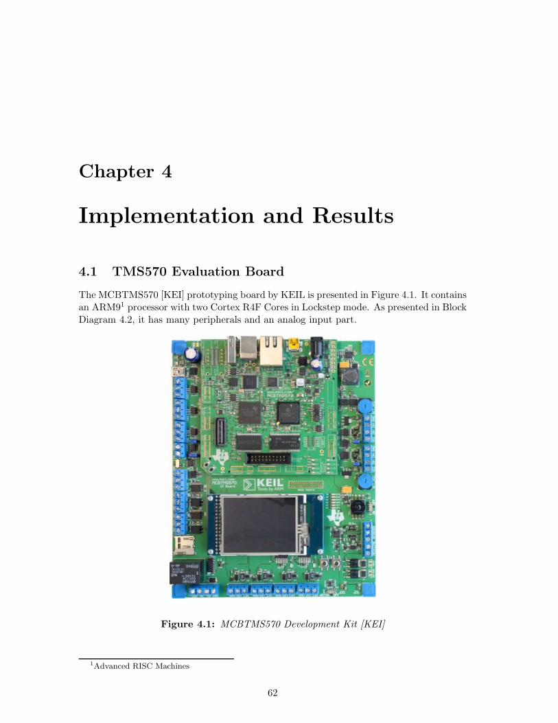
Chapter 4
Implementation and Results
4.1 TMS570 Evaluation Board
The MCBTMS570 [KEI] prototyping board by KEIL is presented in Figure 4.1. It containsan ARM91 processor with two Cortex R4F Cores in Lockstep mode. As presented in BlockDiagram 4.2, it has many peripherals and an analog input part.
Figure 4.1: MCBTMS570 Development Kit [KEI]
1Advanced RISC Machines
62
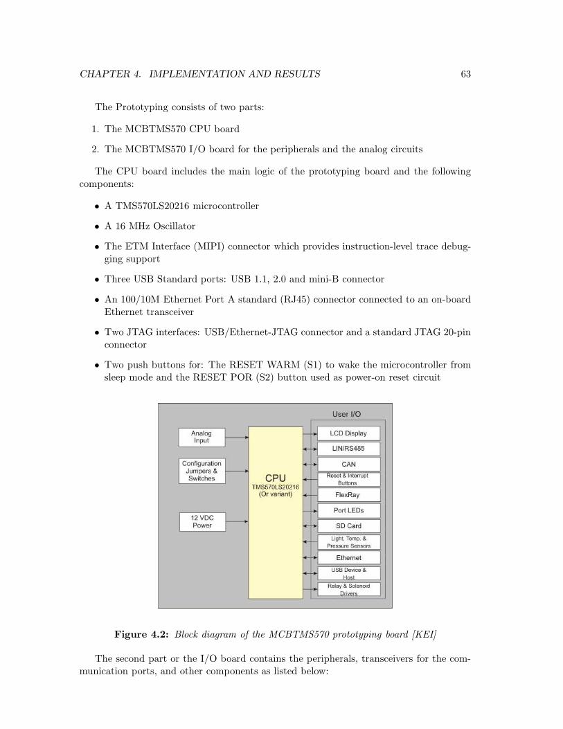
CHAPTER 4. IMPLEMENTATION AND RESULTS 63
The Prototyping consists of two parts:
1. The MCBTMS570 CPU board
2. The MCBTMS570 I/O board for the peripherals and the analog circuits
The CPU board includes the main logic of the prototyping board and the followingcomponents:
• A TMS570LS20216 microcontroller
• A 16 MHz Oscillator
• The ETM Interface (MIPI) connector which provides instruction-level trace debug-ging support
• Three USB Standard ports: USB 1.1, 2.0 and mini-B connector
• An 100/10M Ethernet Port A standard (RJ45) connector connected to an on-boardEthernet transceiver
• Two JTAG interfaces: USB/Ethernet-JTAG connector and a standard JTAG 20-pinconnector
• Two push buttons for: The RESET WARM (S1) to wake the microcontroller fromsleep mode and the RESET POR (S2) button used as power-on reset circuit
Figure 4.2: Block diagram of the MCBTMS570 prototyping board [KEI]
The second part or the I/O board contains the peripherals, transceivers for the com-munication ports, and other components as listed below:
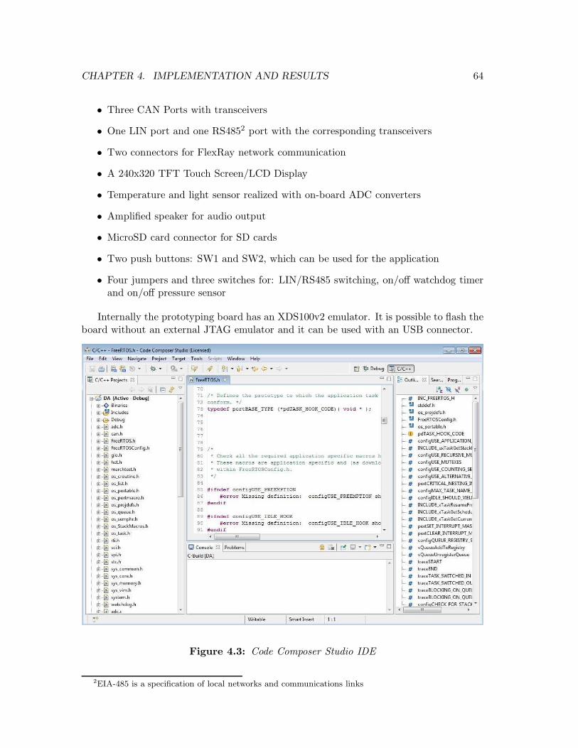
CHAPTER 4. IMPLEMENTATION AND RESULTS 64
• Three CAN Ports with transceivers
• One LIN port and one RS4852 port with the corresponding transceivers
• Two connectors for FlexRay network communication
• A 240x320 TFT Touch Screen/LCD Display
• Temperature and light sensor realized with on-board ADC converters
• Amplified speaker for audio output
• MicroSD card connector for SD cards
• Two push buttons: SW1 and SW2, which can be used for the application
• Four jumpers and three switches for: LIN/RS485 switching, on/off watchdog timerand on/off pressure sensor
Internally the prototyping board has an XDS100v2 emulator. It is possible to flash theboard without an external JTAG emulator and it can be used with an USB connector.
Figure 4.3: Code Composer Studio IDE
2EIA-485 is a specification of local networks and communications links
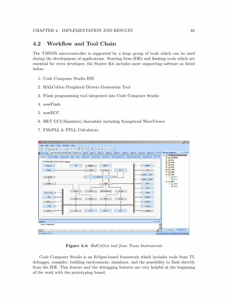
CHAPTER 4. IMPLEMENTATION AND RESULTS 65
4.2 Workflow and Tool Chain
The TMS570 microcontroller is supported by a large group of tools which can be usedduring the development of applications. Starting from IDEs and flashing tools which areessential for every developer, the Starter Kit includes more supporting software as listedbelow:
1. Code Composer Studio IDE
2. HALCoGen Peripheral Drivers Generation Tool
3. Flash programming tool integrated into Code Composer Studio
4. nowFlash
5. nowECC
6. HET GUI/Simulator/Assembler including Synapticad WaveViewer
7. FMzPLL & FPLL Calculators
Figure 4.4: HalCoGen tool from Texas Instruments
Code Composer Studio is an Eclipse-based framework which includes tools from TI,debugger, compiler, building environment, simulator, and the possibility to flash directlyfrom the IDE. This feature and the debugging features are very helpful at the beginningof the work with the prototyping board.
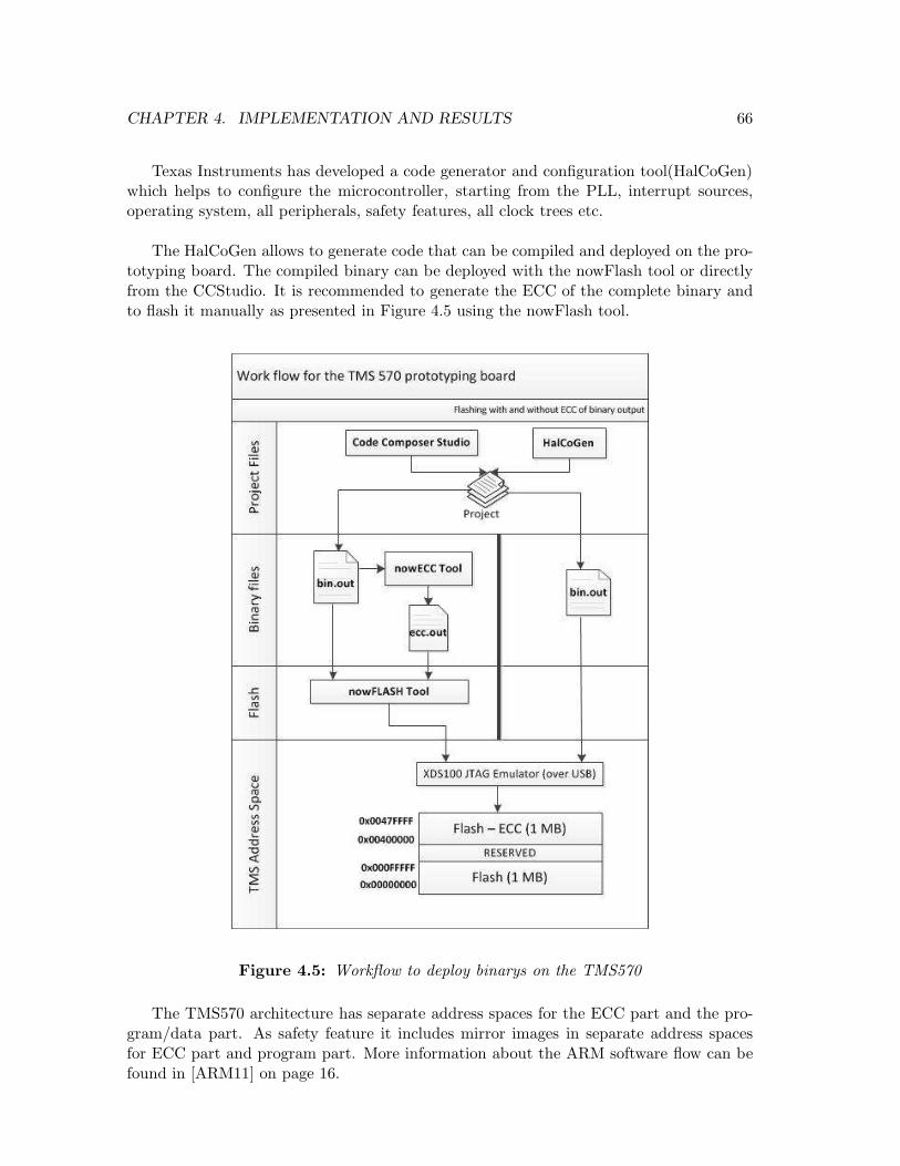
CHAPTER 4. IMPLEMENTATION AND RESULTS 66
Texas Instruments has developed a code generator and configuration tool(HalCoGen)which helps to configure the microcontroller, starting from the PLL, interrupt sources,operating system, all peripherals, safety features, all clock trees etc.
The HalCoGen allows to generate code that can be compiled and deployed on the pro-totyping board. The compiled binary can be deployed with the nowFlash tool or directlyfrom the CCStudio. It is recommended to generate the ECC of the complete binary andto flash it manually as presented in Figure 4.5 using the nowFlash tool.
Figure 4.5: Workflow to deploy binarys on the TMS570
The TMS570 architecture has separate address spaces for the ECC part and the pro-gram/data part. As safety feature it includes mirror images in separate address spacesfor ECC part and program part. More information about the ARM software flow can befound in [ARM11] on page 16.
CHAPTER 4. IMPLEMENTATION AND RESULTS 67
In the support package, three other GUI based tools are included. Two PLL GUI cal-culators for the internal PLL and for the FlexRay PLL can be used to generate values forthe internal PLL registers. The High End Timer Simulator can be used to simulate andconfigure timer functionality like waveforms generators (PWM), memory write triggers,cycle counts etc.
4.3 Start-up Phase
To run the software tests periodically as defined in the concept in Section 3.4, the FreeR-TOS kernel is used, which is an open source and can be provided by the HalCoGen tool,which can be employed to configure tick rate, priorities, task modes, scheduler propertiesand stack/heap size. The OS is responsible for switching between the tests and thereforeit is defined as pre-emptive to let the tasks with higher priority run while the others aresuspended.
In FreeRTOS Tasks [Bar10] are defined with the following function:
portBASE_TYPE xTaskCreate
( pdTASK_CODE pvTaskCode, // Pointer to the Task function
const signed portCHAR * const pcName,// Name of the Task
unsigned portSHORT usStackDepth, // Size of the Task stack
void *pvParameters, // Possible to pass parameters
unsigned portBASE_TYPE uxPriority, // Priority of the Task (1-9)
xTaskHandle *pxCreatedTask // Handle of the created Task
);
The functions are implemented as endless loops with the possibility to suspend aspecific task for a defined time.
void pvTaskCode( void *pvParameters ){
portTickType xLastWakeTime = xTaskGetTickCount();
for(;;) {
vTaskDelayUntil( &xLastWakeTime, (PERIOD_MS / portTICK_RATE_MS ));
}
}
Before the system with the defined safety-related tasks are put into operation, atstart-up, hardware implemented self tests and additional safety measures are carried outfor accuracy. This is necessary to ensure that the device operates normally. At start-up,the sequence of safety tests is as the following:
1. CCM-R4 checks for faults in self test mode by a matching pattern as well as by amismatching pattern.
2. Cortex-R4F core checks for faults using STC/LBIST running all the test patterns.
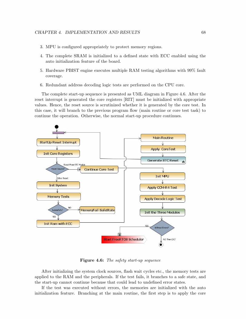
CHAPTER 4. IMPLEMENTATION AND RESULTS 68
3. MPU is configured appropriately to protect memory regions.
4. The complete SRAM is initialized to a defined state with ECC enabled using theauto initialization feature of the board.
5. Hardware PBIST engine executes multiple RAM testing algorithms with 99% faultcoverage.
6. Redundant address decoding logic tests are performed on the CPU core.
The complete start-up sequence is presented as UML diagram in Figure 4.6. After thereset interrupt is generated the core registers [RIT] must be initialized with appropriatevalues. Hence, the reset source is scrutinized whether it is generated by the core test. Inthis case, it will branch to the previous program flow (main routine or core test task) tocontinue the operation. Otherwise, the normal start-up procedure continues.
Figure 4.6: The safety start-up sequence
After initializing the system clock sources, flash wait cycles etc., the memory tests areapplied to the RAM and the peripherals. If the test fails, it branches to a safe state, andthe start-up cannot continue because that could lead to undefined error states.
If the test was executed without errors, the memories are initialized with the autoinitialization feature. Branching at the main routine, the first step is to apply the core
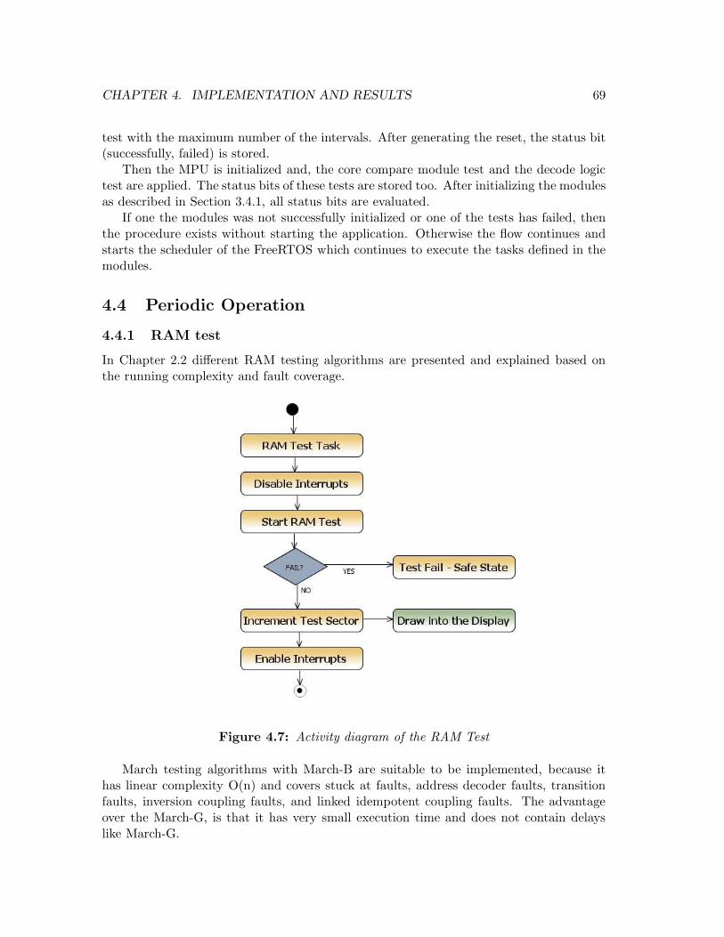
CHAPTER 4. IMPLEMENTATION AND RESULTS 69
test with the maximum number of the intervals. After generating the reset, the status bit(successfully, failed) is stored.
Then the MPU is initialized and, the core compare module test and the decode logictest are applied. The status bits of these tests are stored too. After initializing the modulesas described in Section 3.4.1, all status bits are evaluated.
If one the modules was not successfully initialized or one of the tests has failed, thenthe procedure exists without starting the application. Otherwise the flow continues andstarts the scheduler of the FreeRTOS which continues to execute the tasks defined in themodules.
4.4 Periodic Operation
4.4.1 RAM test
In Chapter 2.2 different RAM testing algorithms are presented and explained based onthe running complexity and fault coverage.
Figure 4.7: Activity diagram of the RAM Test
March testing algorithms with March-B are suitable to be implemented, because ithas linear complexity O(n) and covers stuck at faults, address decoder faults, transitionfaults, inversion coupling faults, and linked idempotent coupling faults. The advantageover the March-G, is that it has very small execution time and does not contain delayslike March-G.
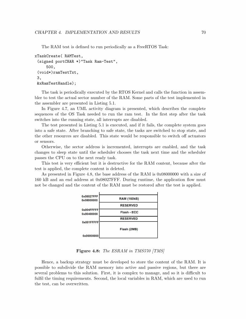
CHAPTER 4. IMPLEMENTATION AND RESULTS 70
The RAM test is defined to run periodically as a FreeRTOS Task:
xTaskCreate( RAMTest,
(signed portCHAR *)"Task Ram-Test",
500,
(void*)ramTestTxt,
3,
&xRamTestHandle);
The task is periodically executed by the RTOS Kernel and calls the function in assem-bler to test the actual sector number of the RAM. Some parts of the test implemented inthe assembler are presented in Listing 5.1.
In Figure 4.7, an UML activity diagram is presented, which describes the completesequences of the OS Task needed to run the ram test. In the first step after the taskswitches into the running state, all interrupts are disabled.
The test presented in Listing 5.1 is executed, and if it fails, the complete system goesinto a safe state. After branching to safe state, the tasks are switched to stop state, andthe other resources are disabled. This state would be responsible to switch off actuatorsor sensors.
Otherwise, the sector address is incremented, interrupts are enabled, and the taskchanges to sleep state until the scheduler chooses the task next time and the schedulerpasses the CPU on to the next ready task.
This test is very efficient but it is destructive for the RAM content, because after thetest is applied, the complete content is deleted.
As presented in Figure 4.8, the base address of the RAM is 0x08000000 with a size of160 kB and an end address at 0x08027FFF. During runtime, the application flow mustnot be changed and the content of the RAM must be restored after the test is applied.
Figure 4.8: The ESRAM in TMS570 [TMS]
Hence, a backup strategy must be developed to store the content of the RAM. It ispossible to subdivide the RAM memory into active and passive regions, but there areseveral problems to this solution. First, it is complex to manage, and so it is difficult tofulfil the timing requirements. Second, the local variables in RAM, which are used to runthe test, can be overwritten.
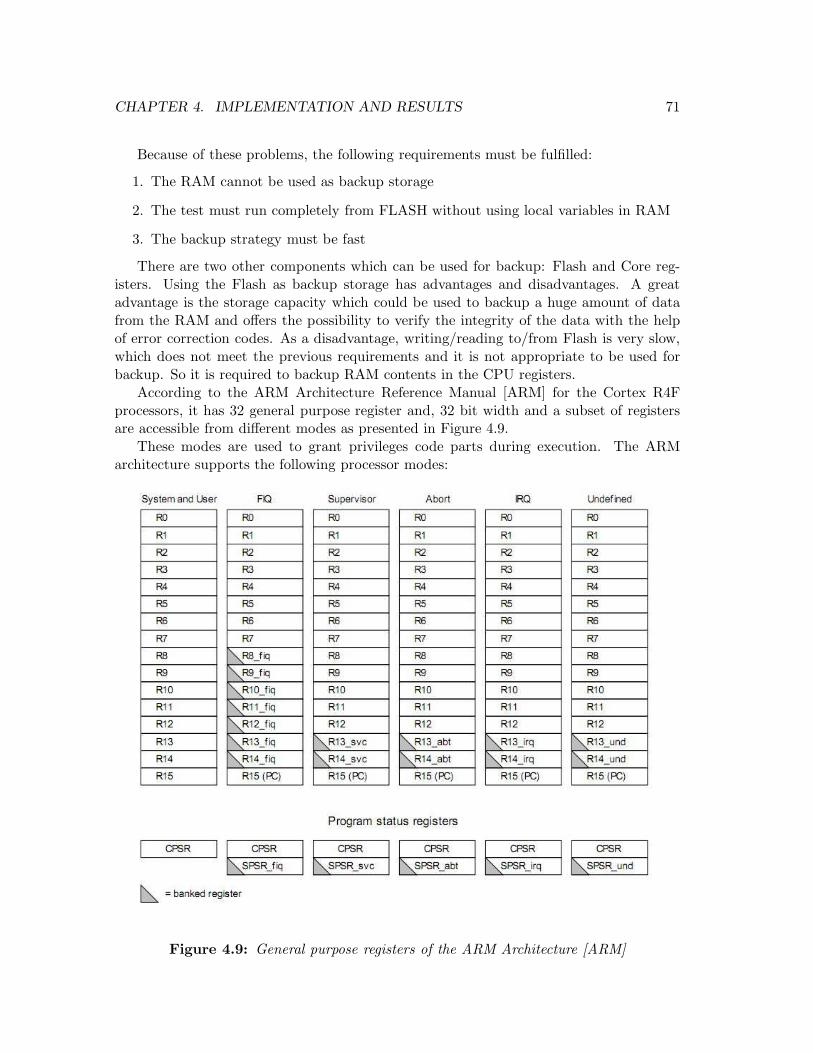
CHAPTER 4. IMPLEMENTATION AND RESULTS 71
Because of these problems, the following requirements must be fulfilled:
1. The RAM cannot be used as backup storage
2. The test must run completely from FLASH without using local variables in RAM
3. The backup strategy must be fast
There are two other components which can be used for backup: Flash and Core reg-isters. Using the Flash as backup storage has advantages and disadvantages. A greatadvantage is the storage capacity which could be used to backup a huge amount of datafrom the RAM and offers the possibility to verify the integrity of the data with the helpof error correction codes. As a disadvantage, writing/reading to/from Flash is very slow,which does not meet the previous requirements and it is not appropriate to be used forbackup. So it is required to backup RAM contents in the CPU registers.
According to the ARM Architecture Reference Manual [ARM] for the Cortex R4Fprocessors, it has 32 general purpose register and, 32 bit width and a subset of registersare accessible from different modes as presented in Figure 4.9.
These modes are used to grant privileges code parts during execution. The ARMarchitecture supports the following processor modes:
Figure 4.9: General purpose registers of the ARM Architecture [ARM]
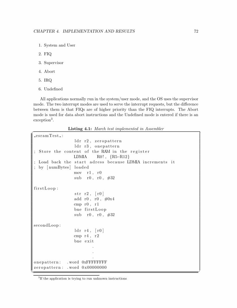
CHAPTER 4. IMPLEMENTATION AND RESULTS 72
1. System and User
2. FIQ
3. Supervisor
4. Abort
5. IRQ
6. Undefined
All applications normally run in the system/user mode, and the OS uses the supervisormode. The two interrupt modes are used to serve the interrupt requests, but the differencebetween them is that FIQs are of higher priority than the FIQ interrupts. The Abortmode is used for data abort instructions and the Undefined mode is entered if there is anexception3.
Listing 4.1: March test implemented in Assembler�
esramTest :l d r r2 , z e r opat te rnl d r r3 , onepattern
; Store the content o f the RAM in the r e g i s t e rLDMIA R0 ! , {R5−R12}
; Load back the s t a r t ad r e s s because LDMIA increments i t; by [ numBytes ] loaded
mov r1 , r0sub r0 , r0 , #32
f i r s tLoop :s t r r2 , [ r0 ]add r0 , r0 , #0x4cmp r0 , r1bne f i r s tLoopsub r0 , r0 , #32
secondLoop :l d r r4 , [ r0 ]cmp r4 , r2bne e x i t
.
.
.onepattern : . word 0xFFFFFFFFzeropat te rn : . word 0x00000000
� �
3If the application is trying to run unknown instructions
CHAPTER 4. IMPLEMENTATION AND RESULTS 73
As presented in Figure 4.9, the user mode, in which 15 registers and the ProgramCounter(PC) are visible is very important. The Stack Pointer(SP) and the Link Register(LR) are mapped on the register R13 and R14.
Thus, the registers R0-R12 can be used as backup storage, and to access these registers,the test will be implemented in Assembler and not in C language, because accessing theseregisters from the assembler is very easy and other assembler instructions for multiple(data at RAM) load and store instructions will be used to move the content from andto RAM. The Cortex R4F Architecture implemented in the TMS570 microcontroller usestwo instruction sets, ARM and Thumb-v2. During the implementation of the test in theAssembler, only ARM mode compatible instructions are used, with the advantage thatthe test can be used in other ARM architectures and because the 32 bit width registersare used as storage with 4 byte access instructions to load/store the content of the RAMmemory.
4.4.2 Watchdog test
In the implementation, the watchdog is used to monitor the program flow. It runs inconjunction with the FreeRTOS Kernel and the application as designed in Section 3.4. Awatchdog reset is carried out periodically within the window size of 200 ms. The testingresults of the current tested sector are displayed on the LCD display.
The application task has the priority of 4. Only the watchdog task has higher prioritybecause in the prototyping board it is not possible to switch it off.
In the running state, the application switches all LEDs present on the board and resetsthe watchdog inside the window.
xTaskCreate( Application,
(signed portCHAR *)"Task Application",
250,
(void*)appText,
4,
&xAppHandle );
After the application task is finished, the next task in ready state is selected by theOS to run. Because the watchdog has the highest priority, it will switch to the watchdogtask and continues to reset the watchdog.
Inside, the lower windows have to be careful not to reset the watchdog, as this wouldreset the complete board.
The timing diagram as illustrated in Figure 4.10 contains two windows:
• Lower window frame with max 10 ms width
• Window frame with min 200 ms
xTaskCreate( Watchdog,
(signed portCHAR *)"Watchdog Task",
250,
(void*)textWatchdog,
8,
&xWatchdogHandle );
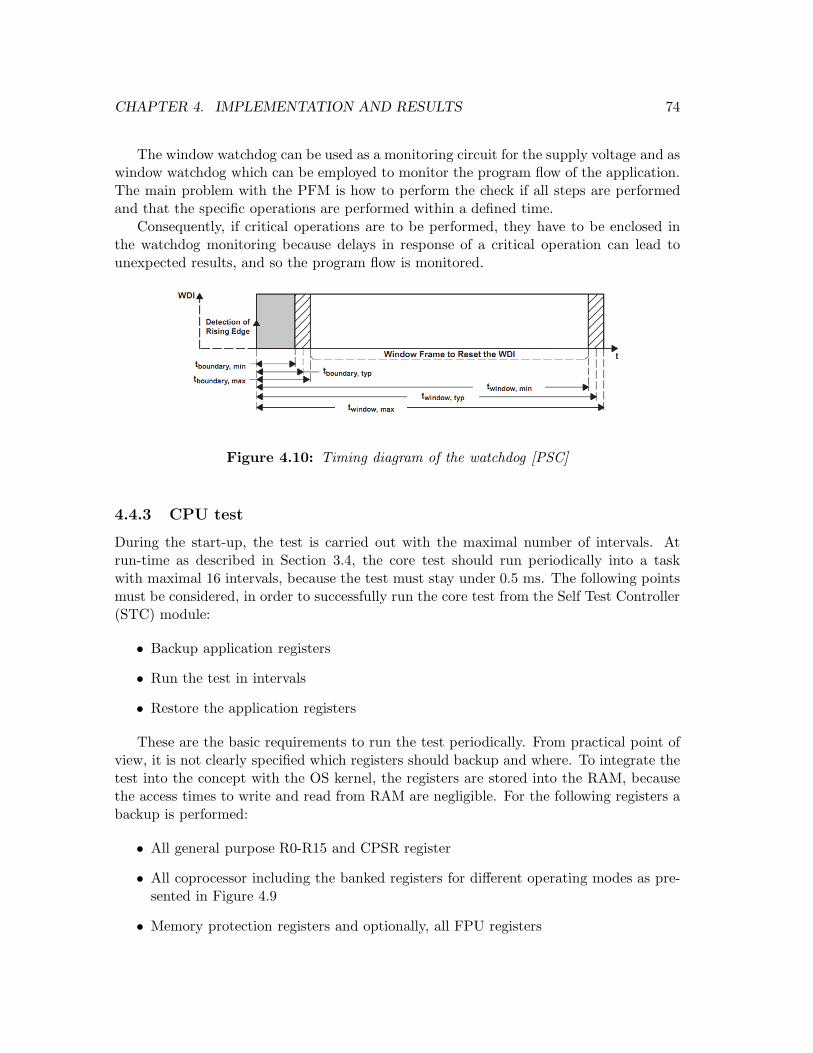
CHAPTER 4. IMPLEMENTATION AND RESULTS 74
The window watchdog can be used as a monitoring circuit for the supply voltage and aswindow watchdog which can be employed to monitor the program flow of the application.The main problem with the PFM is how to perform the check if all steps are performedand that the specific operations are performed within a defined time.
Consequently, if critical operations are to be performed, they have to be enclosed inthe watchdog monitoring because delays in response of a critical operation can lead tounexpected results, and so the program flow is monitored.
Figure 4.10: Timing diagram of the watchdog [PSC]
4.4.3 CPU test
During the start-up, the test is carried out with the maximal number of intervals. Atrun-time as described in Section 3.4, the core test should run periodically into a taskwith maximal 16 intervals, because the test must stay under 0.5 ms. The following pointsmust be considered, in order to successfully run the core test from the Self Test Controller(STC) module:
• Backup application registers
• Run the test in intervals
• Restore the application registers
These are the basic requirements to run the test periodically. From practical point ofview, it is not clearly specified which registers should backup and where. To integrate thetest into the concept with the OS kernel, the registers are stored into the RAM, becausethe access times to write and read from RAM are negligible. For the following registers abackup is performed:
• All general purpose R0-R15 and CPSR register
• All coprocessor including the banked registers for different operating modes as pre-sented in Figure 4.9
• Memory protection registers and optionally, all FPU registers
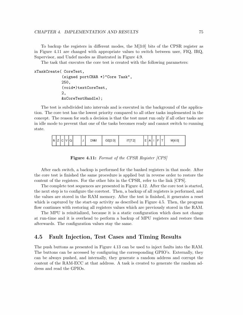
CHAPTER 4. IMPLEMENTATION AND RESULTS 75
To backup the registers in different modes, the M[3:0] bits of the CPSR register asin Figure 4.11 are changed with appropriate values to switch between user, FIQ, IRQ,Supervisor, and Undef modes as illustrated in Figure 4.9.
The task that executes the core test is created with the following parameters:
xTaskCreate( CoreTest,
(signed portCHAR *)"Core Task",
250,
(void*)textCoreTest,
2,
&xCoreTestHandle);
The test is subdivided into intervals and is executed in the background of the applica-tion. The core test has the lowest priority compared to all other tasks implemented in theconcept. The reason for such a decision is that the test must run only if all other tasks arein idle mode to prevent that one of the tasks becomes ready and cannot switch to runningstate.
Figure 4.11: Format of the CPSR Register [CPS]
After each switch, a backup is performed for the banked registers in that mode. Afterthe core test is finished the same procedure is applied but in reverse order to restore thecontent of the registers. For the other bits in the CPSR, refer to the link [CPS].
The complete test sequences are presented in Figure 4.12. After the core test is started,the next step is to configure the coretest. Then, a backup of all registers is performed, andthe values are stored in the RAM memory. After the test is finished, it generates a resetwhich is captured by the start-up activity as described in Figure 4.5. Then, the programflow continues with restoring all registers values which are previously stored in the RAM.
The MPU is reinitialized, because it is a static configuration which does not changeat run-time and it is overhead to perform a backup of MPU registers and restore themafterwards. The configuration values stay the same.
4.5 Fault Injection, Test Cases and Timing Results
The push buttons as presented in Figure 4.13 can be used to inject faults into the RAM.The buttons can be accessed by configuring the corresponding GPIO’s. Externally, theycan be always pushed, and internally, they generate a random address and corrupt thecontent of the RAM-ECC at that address. A task is created to generate the random ad-dress and read the GPIOs.
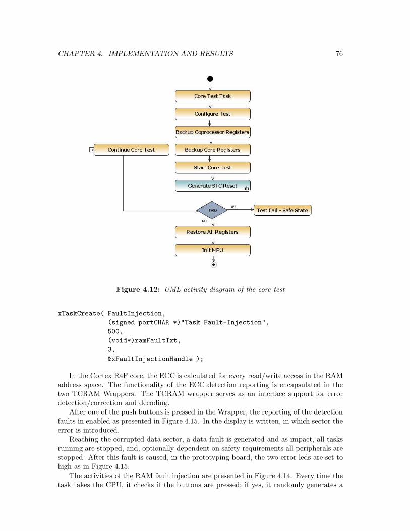
CHAPTER 4. IMPLEMENTATION AND RESULTS 76
Figure 4.12: UML activity diagram of the core test
xTaskCreate( FaultInjection,
(signed portCHAR *)"Task Fault-Injection",
500,
(void*)ramFaultTxt,
3,
&xFaultInjectionHandle );
In the Cortex R4F core, the ECC is calculated for every read/write access in the RAMaddress space. The functionality of the ECC detection reporting is encapsulated in thetwo TCRAM Wrappers. The TCRAM wrapper serves as an interface support for errordetection/correction and decoding.
After one of the push buttons is pressed in the Wrapper, the reporting of the detectionfaults in enabled as presented in Figure 4.15. In the display is written, in which sector theerror is introduced.
Reaching the corrupted data sector, a data fault is generated and as impact, all tasksrunning are stopped, and, optionally dependent on safety requirements all peripherals arestopped. After this fault is caused, in the prototyping board, the two error leds are set tohigh as in Figure 4.15.
The activities of the RAM fault injection are presented in Figure 4.14. Every time thetask takes the CPU, it checks if the buttons are pressed; if yes, it randomly generates a
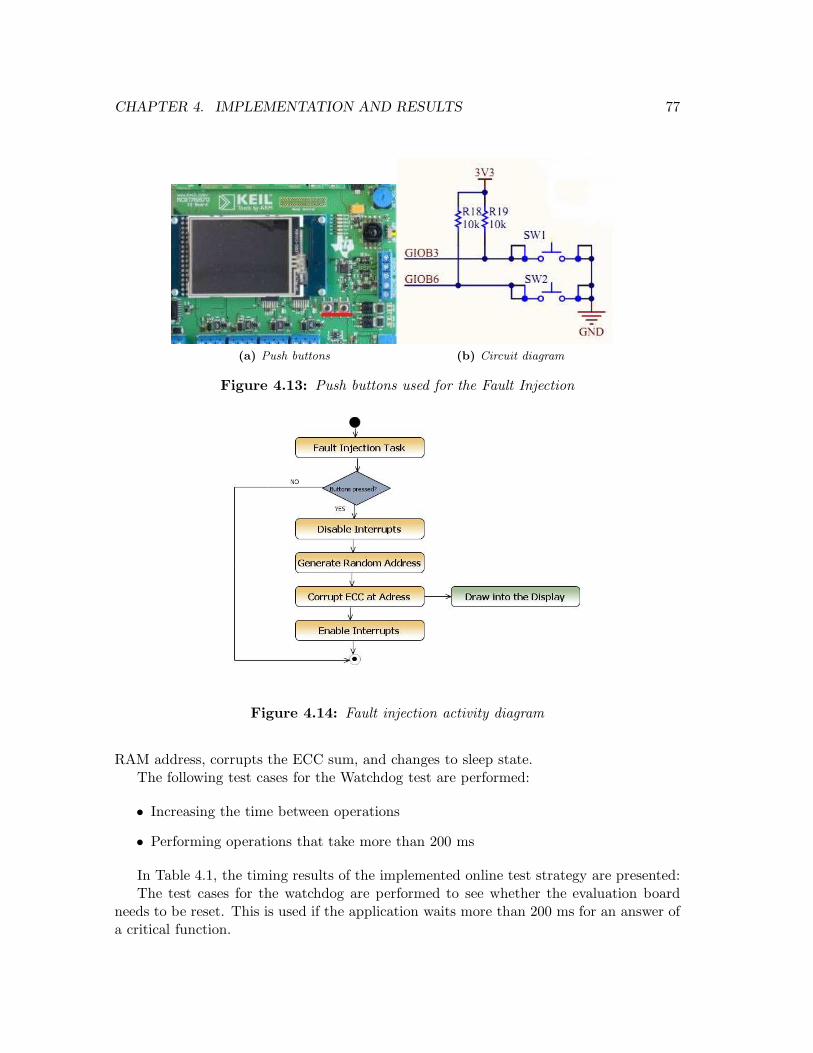
CHAPTER 4. IMPLEMENTATION AND RESULTS 77
(a) Push buttons (b) Circuit diagram
Figure 4.13: Push buttons used for the Fault Injection
Figure 4.14: Fault injection activity diagram
RAM address, corrupts the ECC sum, and changes to sleep state.The following test cases for the Watchdog test are performed:
• Increasing the time between operations
• Performing operations that take more than 200 ms
In Table 4.1, the timing results of the implemented online test strategy are presented:The test cases for the watchdog are performed to see whether the evaluation board
needs to be reset. This is used if the application waits more than 200 ms for an answer ofa critical function.
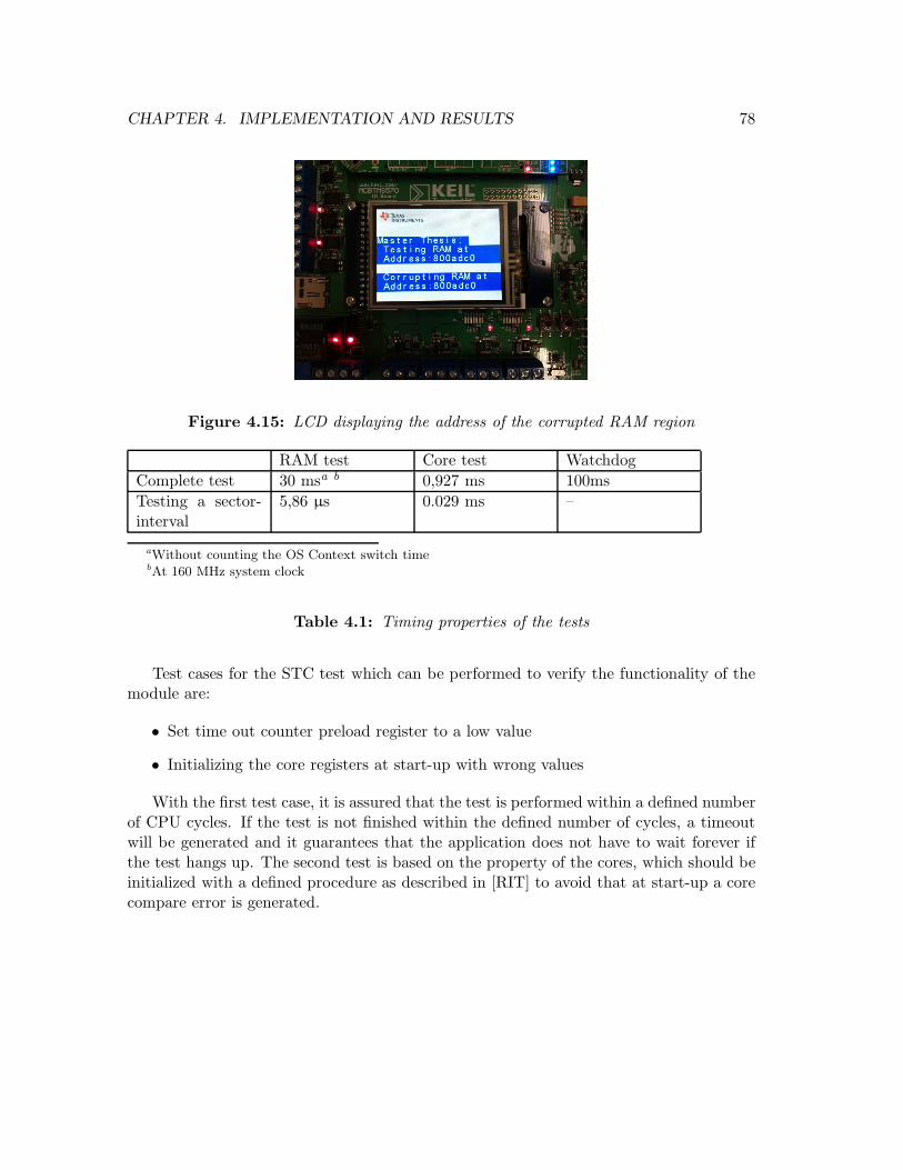
CHAPTER 4. IMPLEMENTATION AND RESULTS 78
Figure 4.15: LCD displaying the address of the corrupted RAM region
RAM test Core test Watchdog
Complete test 30 msa b 0,927 ms 100ms
Testing a sector-interval
5,86 µs 0.029 ms –
aWithout counting the OS Context switch timebAt 160 MHz system clock
Table 4.1: Timing properties of the tests
Test cases for the STC test which can be performed to verify the functionality of themodule are:
• Set time out counter preload register to a low value
• Initializing the core registers at start-up with wrong values
With the first test case, it is assured that the test is performed within a defined numberof CPU cycles. If the test is not finished within the defined number of cycles, a timeoutwill be generated and it guarantees that the application does not have to wait forever ifthe test hangs up. The second test is based on the property of the cores, which should beinitialized with a defined procedure as described in [RIT] to avoid that at start-up a corecompare error is generated.
Chapter 5
Conclusions and Outlook
5.1 Conclusions
At the beginning of this thesis safety-related architectures and self-testing techniques wereintroduced. The beginning was at the hardware level which includes safety strategies andarchitectures with a description of the ideas behind such concepts and also the require-ments these systems must meet to maintain the functional safety.
The form of hardware strategies is dependent on the fault model. A detailed descriptionof such strategies is given, which can be in a form of single and multi-distributed controllers.From a practical point of view, these strategies are concepts which form the base forarchitectures and are described in detail in the second chapter.
In order to assure the safety in a microcontroller, algorithms are needed to be im-plemented, which can be verified either using the mathematical structure or simulation.In the thesis, different algorithms are presented, which can be used in a system to finddifferent types of faults like coupled, stuck-at, transition faults etc. which can be eitherimplemented in hardware as part of an architecture or in software as software-based selftest. However, the main focus was on functional tests.
In order to evaluate such architectures on how they fulfil safety criteria, a list ofevaluation criteria was created. Based on the safety features, performance, run time tests,developing environment etc, the TMS570 microcontroller was chosen as the appropriatedevice for further implementations.
The idea was to use safety features of the microcontroller, and different algorithms tobe mixed in an online periodic testing strategy which assures safety in critical applications.It was shown in the thesis, which are the main safety features of the chosen microcontrollerand which are implemented, the online RAM test and watchdog test running during normalsystem operation.
An operating system kernel was used to run all the tests, and it was shown how thetests can be integrated into a safety strategy, presenting the advantages and disadvantagesof using such a system. As for the performance, the RAM test, which is implementedcompletely in assembler, can be used by any ARM microcontroller with or without anoperating system.
A microcontroller which has not only off-line safety features (tests that can be per-formed only at startup) but online features as well, which tests the microcontroller’s
79
CHAPTER 5. CONCLUSIONS AND OUTLOOK 80
functional parts like RAM, CPU, flash, would extend the possibility for critical applica-tions that could be implemented in the automotive industry or power plants, medical lifesupport equipment etc.
5.2 Outlook
The TMS570 microcontroller offers a variety of tests and safety features which can beused during the development. As presented in the design chapter of the concept, it hassome drawbacks because it does not have tests for every part of the system which can beperformed at runtime. All RAM tests can be performed only at start-up, and the RAMneeds to be extended either with hardware or with software tests for such purposes.
Such an integration would be a powerful feature for all applications in that field. Notonly by extending such tests, but also by creating a better OS support for the safetyfeatures like the core test, as maintaining and backup the different registers in software toperform the test periodically is error prone because of timing requirements.
There are new microcontrollers with safety features which have more computing coresand adequately address the requirements of safety-critical applications. They will be usedin the automotive industry in the near future.
Appendix A
Definitions
A.1 Abbreviations
ATPG Automatic Test Pattern GenerationAF Address Decoder FaultsALU Arithmetical Logical UnitARM Advanced RISC MachineASIC Application Specific Integrated CircuitASIL Automotive Safety Integrity LevelBIST Built in Self TestsCAN Controller Area NetworkCCF Common Cause FailuresCPU Central Processing UnitCPSR Current Program Status RegisterCF Coupling FaultsCFin Inversion Coupling FaultCFid Idempotent Coupling FaultCFst State Coupling FaultCU Comparing UnitDC Diagnostic CoverageDRF Data Retention FaultDSP Digital Signal ProcessorEEPROM Electrically Erasable Programmable Read-Only MemoryECC Error Correction CodesESM Error Signaling ModuleETM Embedded Trace MacrocellFMzPLL Frequency modulated phase lock loopFPLL Flexray phase lock loopFSM Finite State MachineFPU Floating Point UnitFMEA Failure Modes and Effects AnalysisGALPAT Galloping PatternGUI Graphical user interface
81
APPENDIX A. DEFINITIONS 82
HALCoGen Hardware Abstraction Code Generator LayerHET High-End TimerISA Instruction Set ArchitectureIDE Integrated Development EnvironmentITI Institute for Technical InformaticsJTAG Joint Test Action Group InterfaceLBIST Logical Built-in Self TestsLIN Local Interconnect NetworkMIPI Mobile Industry Processor InterfaceMEPAS Methods and processes for automotive embedded software development,verification and validationMPU Memory Protection UnitMCU Microcontroller UnitNowECC Error Correction Code GeneratorPWM Pulse Width ModulationPFM Program Flow MonitoringPCP Peripheral Control ProcessorPBIST Programmable Built-In Self TestRAM Random Access MemoryRISC Reduced Instruction Set ComputingROM Read Only MemoryRTOS Real Time Operating SystemRTL Register Transfer LevelRJ45 Registered JackSRS Safety Requirements SpecificationSIL Safety Integrity LevelSAF Stuck-at FaultsSFF Safe Failure FractionSMP Symmetric multiprocessor architecturesSOF Stuck-open faultSTC Self Test ControllerSFF Safe Failure FractionSBST Software Based Self TestsTCRAM Tightly Coupled Random Access MemoryTI Texas InstrumentsTLP Thread Level ParallelismTF Transition FaultsThWD TTOSHIBA hW diagnosticTFT-LCD Thin Film Transistor Liquid Crystal DisplayWALPAT Walking Pattern
APPENDIX A. DEFINITIONS 83
A.2 Used Symbols
λS Rate of Safe FailuresλD Rate of Dangerous FailuresλD Rate of Dangerous Failures that are Detected⇓ Decreasing Addressing Order⇑ Increasing Addressing Order(w0) Write Zero to the Specific Ram Cell(w1) Write One to the Specific Ram Cell(r0) Read Zero to the Specific Ram Cell(r1) Read One to the Specific Ram Cell↓ Forced Transition from 1 to 0↑ Forced Transition from 0 to 1
Bibliography
[AGPP09] Andreas Apostolakis, Dimitris Gizopoulos, Mihalis Psarakis, and AntonisPaschalis. Software-Based Self-Testing of Symmetric Shared-Memory Mul-tiprocessors. IEEE Transactions on Computers, 58:1682 – 1694, 2009.
[APG+09] Andreas Apostolakis, Mihalis Psarakis, Dimitris Gizopoulos, AntonisPaschalis, and Ishwar Parulkar. Exploiting Thread-Level Parallelism in Func-tional Self-Testing of CMT Processors. European Test Symposium, pages 33– 38, 2009.
[ARM] ARM architecture reference manual.
[ARM11] ARM Optimizing C/C++ Compiler v4.9, August 2011.
[Bar10] Richard Barry. Using the FreeRTOS Real Time Kernel. 2010.
[BBC+08] Alfredo Benso, Alberto Bosio, Stefano Di Carlo, Giorgio Di Natale, and PaoloPrinetto. March Test Generation Revealed. IEEE Transactions on Comput-ers, VOL. 57, NO. 12, 2008.
[BCM07] Gabriele Boschi, Federico Colucci, and Riccardo Mariani. Using an innova-tive SoC-level FMEA methodology to design in compliance with IEC61508.Design, Automation & Test in Europe Conference & Exhibition, 2007.
[BFM+03] Massimo Baleani, Alberto Ferrari, Leonardo Mangeruca, Allberto Luigi San-giovanni Vincentelli, Maurizio Peri, and Saverio Pezzini. Falut-Tolerant Plat-forms for Automotive Safety-Critical Applications. Proceedings of the 2003International Conference on Compilers, Architecture and Synthesis for Em-bedded Systems, pages 170 – 177, 2003.
[BHW06] Ismet Bayraktaroglu, Jim Hunt, and Daniel Watkins. Cache Resident Func-tional Microprocessor Testing: Avoiding High Speed IO Issues. Test Confer-ence, ITC ’06. IEEE International, pages 1 – 7, 2006.
[BSE07] Simon Brewerton, Rolf Schneider, and Denis Eberhard. Implementation of aBasic Single-Microcontoller Monitoring Concept for Safety Critical Systemson a Dual-Core Microcontroller. In SAE International-Safety Critical Sys-tems, Paper Number: 2007-01-1486, 2007.
[CPS] Cortex-R4 and Cortex-R4F Technical Reference Manualhttp://www.arm.com/products/processors/cortex-r/index.php.
84
BIBLIOGRAPHY 85
[CRRD03] Li Chen, Srivaths Ravi, Anand Raghunathan, and Sujit Dey. A ScalableSoftware-Based Self-Test Methodology for Programmable Processors. In Proc.40th Design Automation Conference, pages 548–553, 2003.
[CWLG07] Chung-Ho Chen, Chih-Kai Wei, Tai-Hua Lu, and Hsun-Wei Gao. SoftwareBased Self-Testing with Multiplie-Level Abstractions for Soft Processor Cores.IEEE Very Large Scale Integration Systems (VLSI), 15:505–517, 2007.
[FM07] Peter Fuhrmann and Riccardo Mariani. Comparing fail-safe microcontrollerarchitectures in light of IEC 61508. In 22nd IEEE International Symposiumon Defect and Fault-Tolerance in VLSI Systems, 2007.
[Goo93] Ad J. Van De Goor. Using March Tests to Test SRAMs. IEEE Design andTest of Computers, vol. 10 no. 1:8–14, 1993.
[GVA06] Sankar Gurumurthy, Shobha Vasudevan, and Jacob A. Abraham. Automaticgeneration of instruction sequences targeting hard-to-detect structural faultsin a processor. In IEEE International Test Conference, pages 1 – 9, 2006.
[HA99] Mohamed S. Hefny and Hassanein H. Ammer. Design of an improved watch-dog circuit for microcontroller-based systems. ICM’99. Eleventh InternationalConference on Microelectronics, pages 165 – 168, 1999.
[Has] Atsushi Hasegawa. R&D strategy: Using various types of multi-core architec-tures to overcome limitations of single-core microcomputers. Technical report,RENESAS.
[KEI] http://www.keil.com/support/man/docs/mcbtms570/.
[KLC+02] Angela Krstic, Wei-Cheng Lai, Kwang-Ting Cheng, Li Chen, and Sujit Dey.Embedded Software Based Self Test for Programmable Core Based Designs.IEEE Design & Test, 19:18–27, 2002.
[KPGX05] Nektarios Kranitis, Antonis Paschalis, Dimitris Gizopoulos, and George Xe-noulis. Software-based self-testing of embedded processors. IEEE Transac-tions on Computers, 54 Issue: 4:461 – 475, 2005.
[KS06] Thomas Kottke and Andreas Steininger. A Reconfigurable Generic Dual-CoreArchitecture. International Conference on Dependable Systems and Networks,pages 45 – 54, 2006.
[LCD+05] Eldon G. Leaphart, Barbara J. Czerny, Joseph G. D’Ambrosio, Christopher L.Denlinger, and Deron Littlejohn. Survey of Software Failsafe Techniques forSafety-Critical Automotive Applications. SAE 2005 World Congress & Exhi-bition, April 2005, Detroit, MI, USA, Session: Safety-Critical Systems (Part1 & 2), 2005.
[Mar07] Riccardo Mariani. Applying IEC 61508 to Integrated Circuits. Technicalreport, 2007.
BIBLIOGRAPHY 86
[MB07] Riccardo Mariani and Gabriele Boschi. A systematic approach for FailureModes and Effects Analysis of System-On-Chips. 13th IEEE InternationalOn-Line Testing Symposium, pages 187 – 188, 2007.
[MKS10] Riccardo Mariani, Thomas Kuschel, and Hiroshi Shigehara. A flexible mi-crocontroller architecture for fail-safe and fail-operational systems. Technicalreport, 2010.
[Mon99] Sergio Montenegro. Sichere und fehlertolerante Steuerungen - Entwicklungsicherheitsrelevanter Systeme. Carl Hanser Verlag Munchen Wien, 1999.
[NTA78] R. Nair, Satish M. Thatte, and Jacob A. Abraham. Efficient Algorithmsfor Testing Semiconductor Random-Access Memories. IEEE Transactions onComputers, pages 572 – 576, 1978.
[PG04] Antonis Paschalis and Dimitris Gizopoulos. Effective Software-Based Self-Test Strategies for On-Line Periodic Testing of Embedded Processors. IEEETransactions on Computer-Aided Design of Integrated Circuits and Systems,2004.
[PGH+06] Mihalis Psarakis, Dimitris Gizopoulos, Miltiadis Hatzimihail, AntonisPaschalis, Anand Raghunathan, and Srivaths Ravi. Systematic Software-Based Self-Test for Pipelined Processors. 2006.
[PGK+01] Antonis M. Paschalis, Dimitris Gizopoulos, Nektarios Kranitis, MihalisPsarakis, and Yervant Zorian Zorian. Deterministic Software-Based Self-Testing of Embedded Processor Cores. In Design, Automation and Test inEurope. Conference and Exhibition, pages 92 – 96, 2001.
[PGSR10] Mihalis Psarakis, Dimitris Gizopoulos, Ernesto Sanchez, and Matteo SonzaReorda. Microprocessor Software-Based Self-Testing. IEEE Design and Testof Computers, vol. 27, no. 3:pages 4–19, 2010.
[PML02] Praveen Parvathala, Kaila Maneparambil, and William Lindsay. FRITS - Amicroprocessor functional BIST method. ITC ’02 Proceedings of the 2002IEEE International Test Conference, pages 590 – 598, 2002.
[PSC] Processor Supervisory Circuits with Window-Watchdog”http://www.ti.com/lit/ds/symlink/tps3813l30.pdf”.
[RIT] Recommended Initializations for TMS570 Microcontrollers -http://www.ti.com/lit/an/spna119/spna119.pdf.
[RSCS04] Matteo Sonza Reorda, Giovanni Squillero, Fulvio Corno, and Ernesto Sanchez.Automatic Test Program Generation: A Case Study. Design & Test of Com-puters, IEEE, 21 Issue: 2:102 – 109, 2004.
[SA98] Jian Shen and Jacob A. Abraham. Native Mode Functional Test Generationfor Processors with Applications to Self Test and Design Validation. TestConference Proceedings, International, pages 990 – 999, 1998.
BIBLIOGRAPHY 87
[SD06] Padma Sundaram and Joseph G. D’Ambrosio. Controller Integrity in Au-tomotive Failsafe System Architectures. In Safety Critical Systems, SpecialPublications Paper Collections, SAE International, Product Code: SP-2029,2006.
[TMS] TMS570 Technical Reference Manual.
[TP07] Thomas Tamandl and Peter Preininger. Online Self Tests for Microcontrollersin Safety Related Systems. In 5th IEEE International Conference on Indus-trial Informatics, pages 137 – 142, 2007.
[Tum09] Peter Tummeltshammer. Analysis of Common Cause Faults in Dual CoreArchitectures. PhD thesis, Technische Universitat Wien - Fakultat fur Infor-matik, 2009.
[WWC+05] Charles H. P. Wen, Li-C. Wang, Kwang-Ting Cheng, Kai Yang, Wei-TingLiu, and Ji-Jan Chen. On a software-based self-test methodology and itsapplication. In VLSI Test Symposium, 2005. Proceedings. 23rd IEEE, pages107 – 113, 2005.
[WWW06] Laung-Terng Wang, Cheng-Wen Wu, and Xiaoqing Wen. VLSI Test Princi-ples and Architectures - Design for Testability. Morgan Kaufmann; 1 edition,2006.

![E[M]CONOMY moves! - ilg-sulzberger.de Die EMCO Group ist ein Verbund von Topanbietern aus der Werkzeugmaschinenbranche. ... CONCEPT MILL 55 CONCEPT MILL 105 CONCEPT MILL 250 CONCEPT](https://img.pdfslide.org/doc/110x75/5b02e7647f8b9a3c378b639e/emconomy-moves-ilg-emco-group-ist-ein-verbund-von-topanbietern-aus-der-werkzeugmaschinenbranche.jpg)