Embed Size (px)
Citation preview
Die Bedeutung interferometerischerMesstechnik für die MikroOptik
Reinhard Völkel, Martin Eisner, Kenneth J. Weible
SUSS MicroOptics, Neuchâtel Schweiz
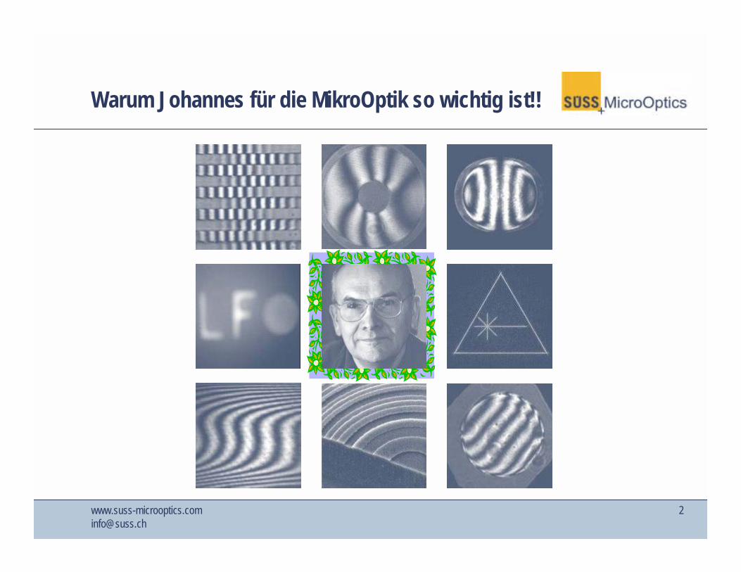
Warum ist Messtechnik für MikroOptik so wichtig?Warum Johannes für die MikroOptik so wichtig ist!!
1987
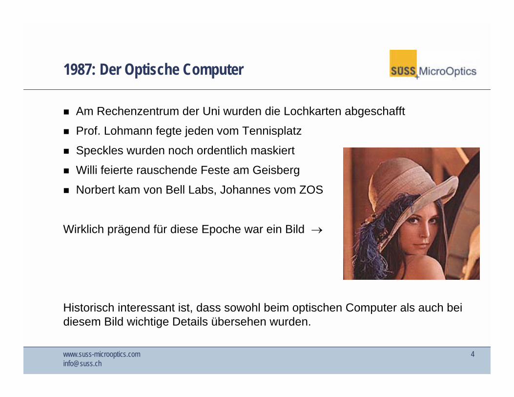
1987: Der Optische Computer
! Am Rechenzentrum der Uni wurden die Lochkarten abgeschafft
! Prof. Lohmann fegte jeden vom Tennisplatz
! Speckles wurden noch ordentlich maskiert
! Willi feierte rauschende Feste am Geisberg
! Norbert kam von Bell Labs, Johannes vom ZOS
Wirklich prägend für diese Epoche war ein Bild →
Historisch interessant ist, dass sowohl beim optischen Computer als auch beidiesem Bild wichtige Details übersehen wurden.
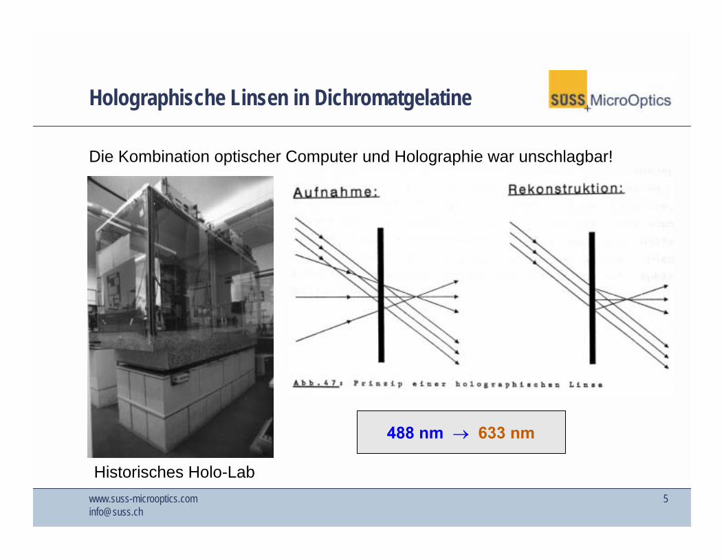
Holographische Linsen in Dichromatgelatine
Die Kombination optischer Computer und Holographie war unschlagbar!
Historisches Holo-Lab
488 nm → 633 nm
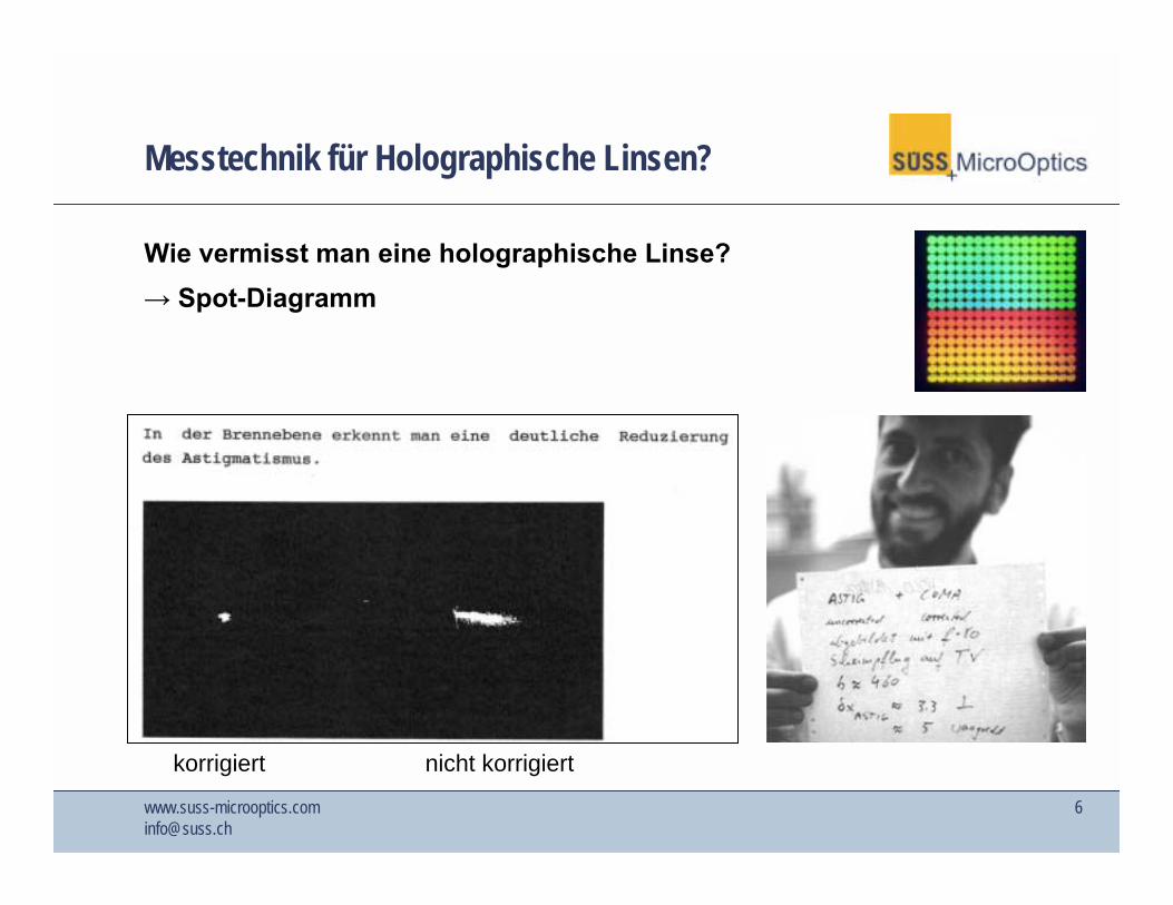
→ Spot-DiagrammWie vermisst man eine holographische Linse?
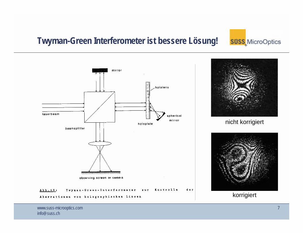
Messtechnik für Holographische Linsen?
nicht korrigiertkorrigiert
1992
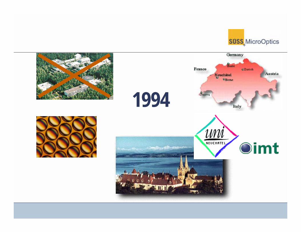
1994
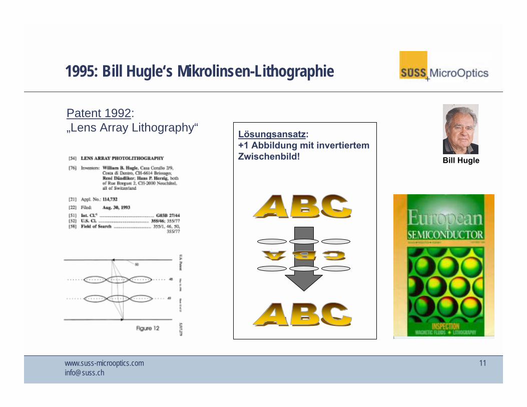
1995: Bill Hugle‘s Mikrolinsen-Lithographie
Bill Hugle
Patent 1992:„Lens Array Lithography“ Lösungsansatz:
+1 Abbildung mit invertiertemZwischenbild!
h‘
h1Principle Ray
L1 L2
OBJ IMAG
Telescope I Telescope II
EL2EL1
Field Aperture
System Aperture
h1
h‘
h1h1Principle Ray
L1 L2
OBJ IMAG
Telescope I Telescope II
EL2EL1
Field Aperture
System Aperture
h1h1
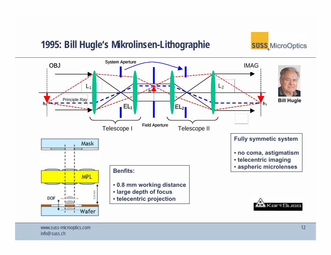
1995: Bill Hugle‘s Mikrolinsen-Lithographie
Bill Hugle
Benfits:
• 0.8 mm working distance• large depth of focus• telecentric projection
Fully symmetic system
• no coma, astigmatism• telecentric imaging• aspheric microlenses
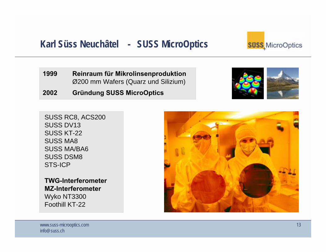
Karl Süss Neuchâtel - SUSS MicroOptics
1999 Reinraum für MikrolinsenproduktionØ200 mm Wafers (Quarz und Silizium)
2002 Gründung SUSS MicroOptics
SUSS RC8, ACS200SUSS DV13SUSS KT-22SUSS MA8SUSS MA/BA6SUSS DSM8STS-ICP
TWG-InterferometerMZ-InterferometerWyko NT3300Foothill KT-22
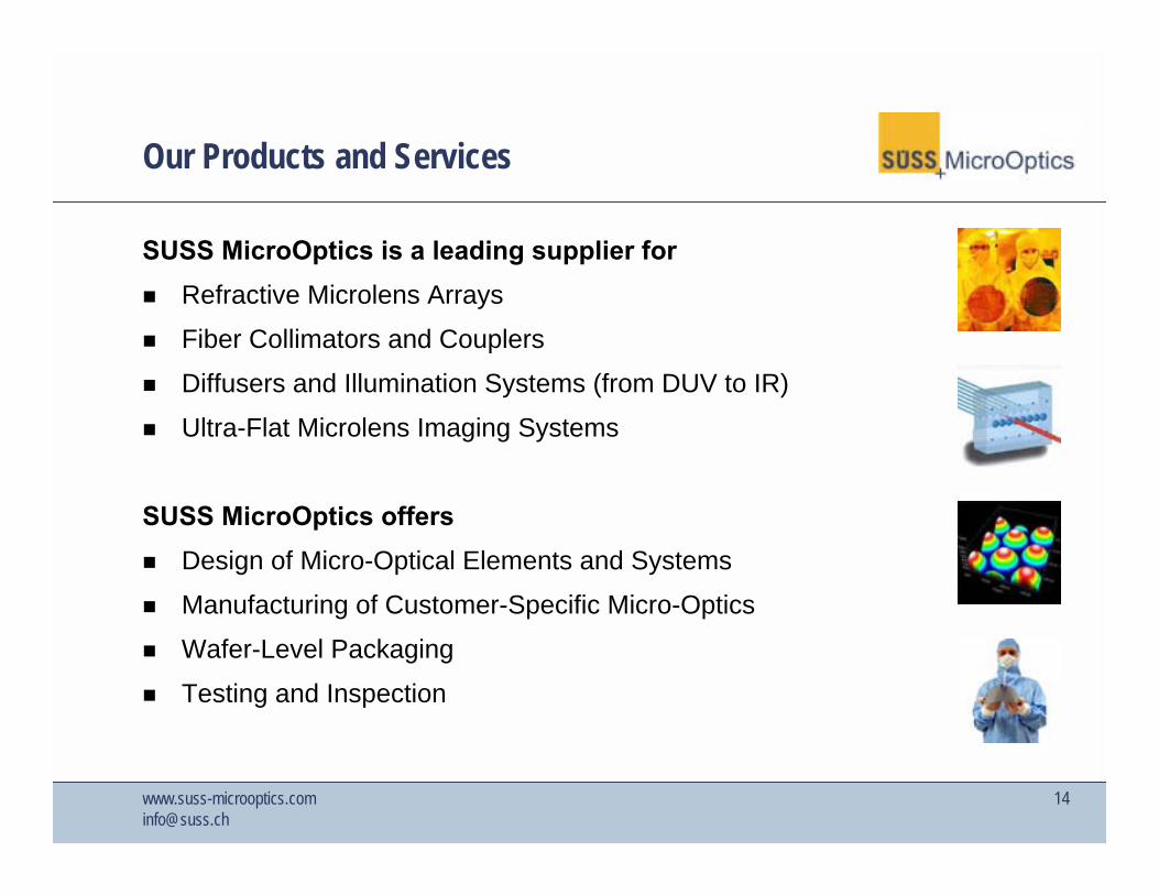
Our Products and Services
SUSS MicroOptics is a leading supplier for ! Refractive Microlens Arrays
! Fiber Collimators and Couplers
! Diffusers and Illumination Systems (from DUV to IR)
! Ultra-Flat Microlens Imaging Systems
SUSS MicroOptics offers ! Design of Micro-Optical Elements and Systems
! Manufacturing of Customer-Specific Micro-Optics
! Wafer-Level Packaging
! Testing and Inspection
Optical Design - Consulting
SUSS MicroOptics profits from more than 15 years experience in the design of optical elements (diffractive and refractive) and optical systems.
SUSS MicroOptics uses the following design tools
! SILVACO Expert, IC Layout Editor (Mask-Layout)! ZEMAX-EE, Optical Design Program! RAYTRACE, Optical Design Program! Simulated Annealing and Iterative Fourier Optimization for DOEs! Rigorous Diffraction Theory for Wave Propagation
SUSS MicroOptics works closely with top-ranking research groups worldwide to support our customers in developing and improving their products.
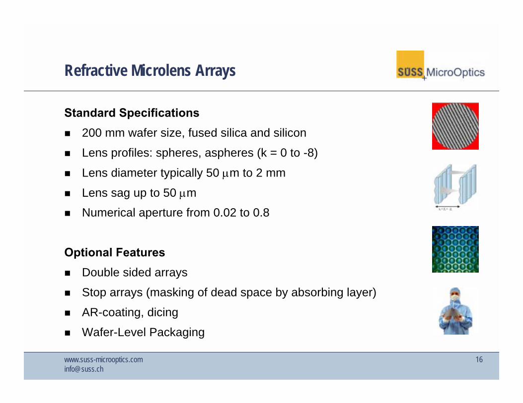
Refractive Microlens Arrays
Standard Specifications! 200 mm wafer size, fused silica and silicon
! Lens profiles: spheres, aspheres (k = 0 to -8)
! Lens diameter typically 50 µm to 2 mm
! Lens sag up to 50 µm
! Numerical aperture from 0.02 to 0.8
Optional Features! Double sided arrays
! Stop arrays (masking of dead space by absorbing layer)
! AR-coating, dicing
! Wafer-Level Packaging
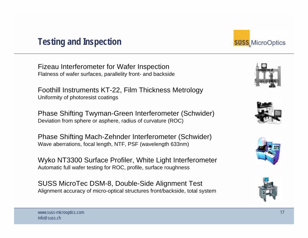
Testing and Inspection
Fizeau Interferometer for Wafer InspectionFlatness of wafer surfaces, parallelity front- and backside
Foothill Instruments KT-22, Film Thickness MetrologyUniformity of photoresist coatings
Phase Shifting Twyman-Green Interferometer (Schwider)Deviation from sphere or asphere, radius of curvature (ROC)
Phase Shifting Mach-Zehnder Interferometer (Schwider)Wave aberrations, focal length, NTF, PSF (wavelength 633nm)
Wyko NT3300 Surface Profiler, White Light InterferometerAutomatic full wafer testing for ROC, profile, surface roughness
SUSS MicroTec DSM-8, Double-Side Alignment TestAlignment accuracy of micro-optical structures front/backside, total system
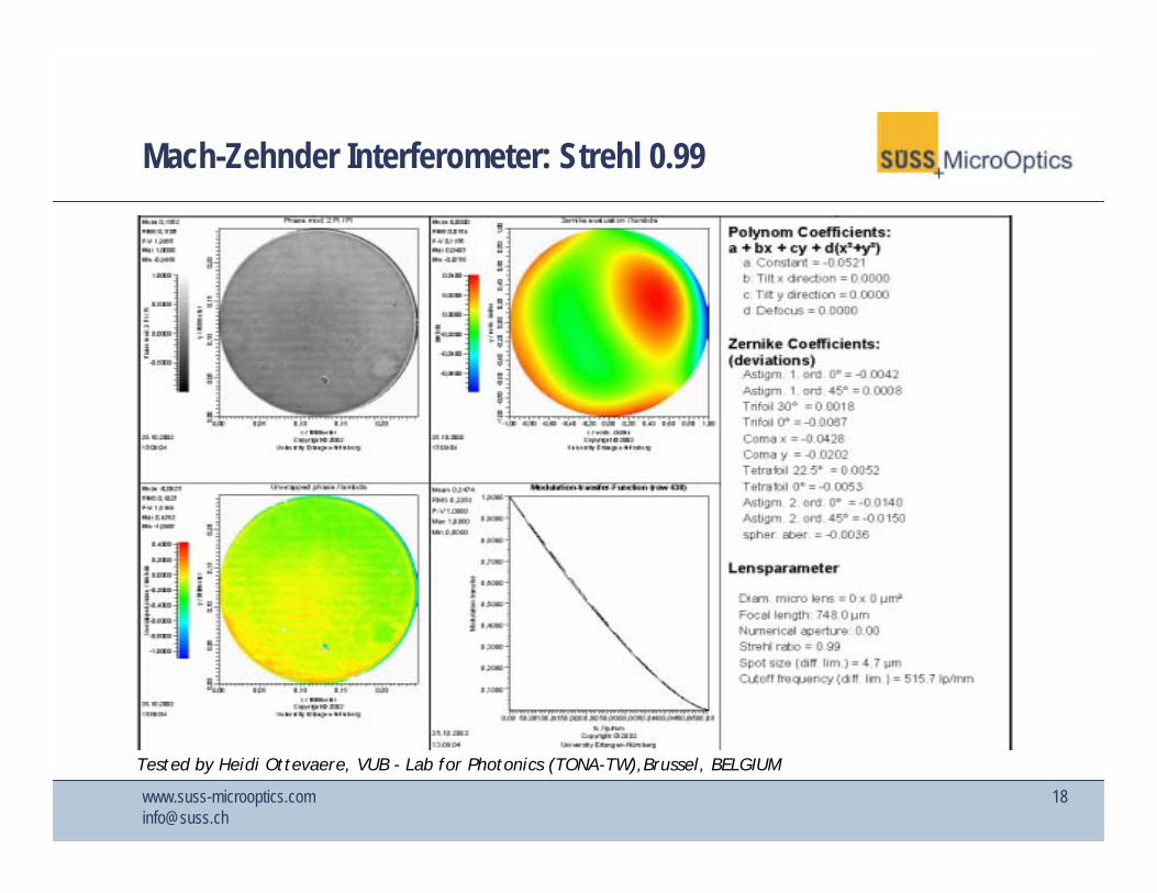
Mach-Zehnder Interferometer: Strehl 0.99
Tested by Heidi Ottevaere, VUB - Lab for Photonics (TONA-TW),Brussel, BELGIUM
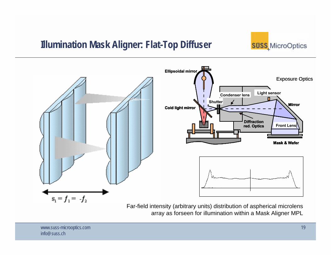
Illumination Mask Aligner: Flat-Top Diffuser
Exposure OpticsEllipsoidal mirror
ShutterCondenser lens Light sensor
Mask & Wafer
Mirror
Diffractionred. Optics Front Lens
rrorCold light mi
Exposure OpticsEllipsoidal mirror
ShutterCondenser lens Light sensor
Mask & Wafer
Mirror
Diffractionred. Optics Front Lens
rrorCold light mi
Ellipsoidal mirrorEllipsoidal mirror
ShutterShutterCondenser lensCondenser lens Light sensorLight sensor
Mask & WaferMask & Wafer
MirrorMirror
Diffractionred. OpticsDiffractionred. Optics Front LensFront Lens
rrorCold light mirrorCold light mi
Far-field intensity (arbitrary units) distribution of aspherical microlens array as forseen for illumination within a Mask Aligner MPL
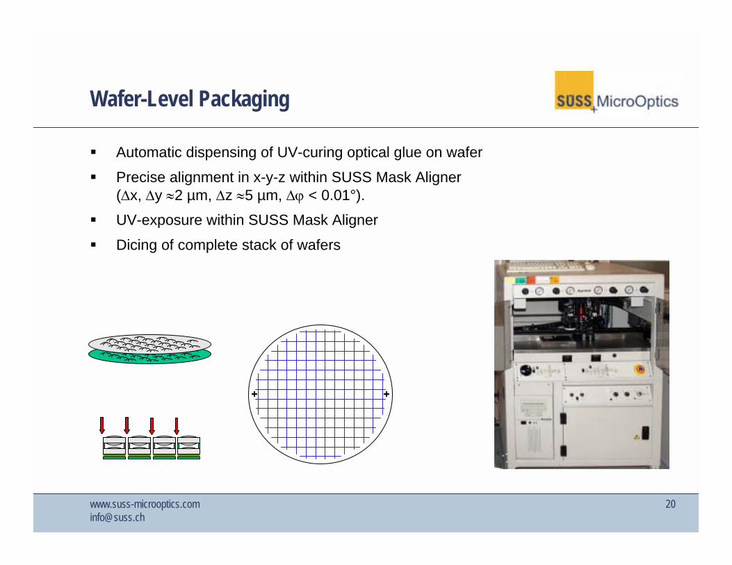
Wafer-Level Packaging
" Automatic dispensing of UV-curing optical glue on wafer
" Precise alignment in x-y-z within SUSS Mask Aligner (∆x, ∆y ≈2 µm, ∆z ≈5 µm, ∆ϕ < 0.01°).
" UV-exposure within SUSS Mask Aligner
" Dicing of complete stack of wafers
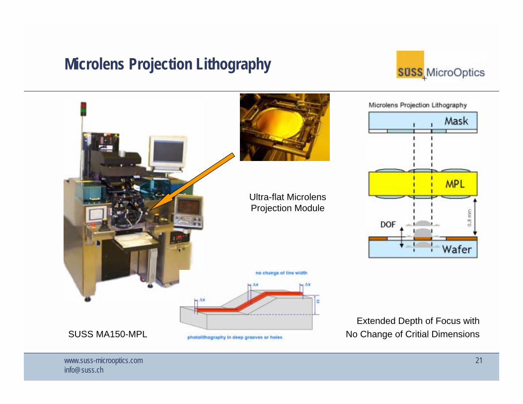
Microlens Projection Lithography
SUSS MA150-MPL
Ultra-flat Microlens Projection Module
Extended Depth of Focus withNo Change of Critial Dimensions
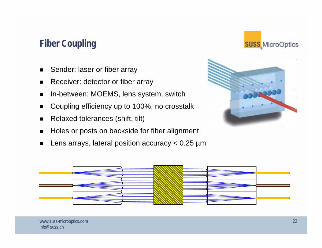
Fiber Coupling
! Sender: laser or fiber array
! Receiver: detector or fiber array
! In-between: MOEMS, lens system, switch
! Coupling efficiency up to 100%, no crosstalk
! Relaxed tolerances (shift, tilt)
! Holes or posts on backside for fiber alignment
! Lens arrays, lateral position accuracy < 0.25 µm
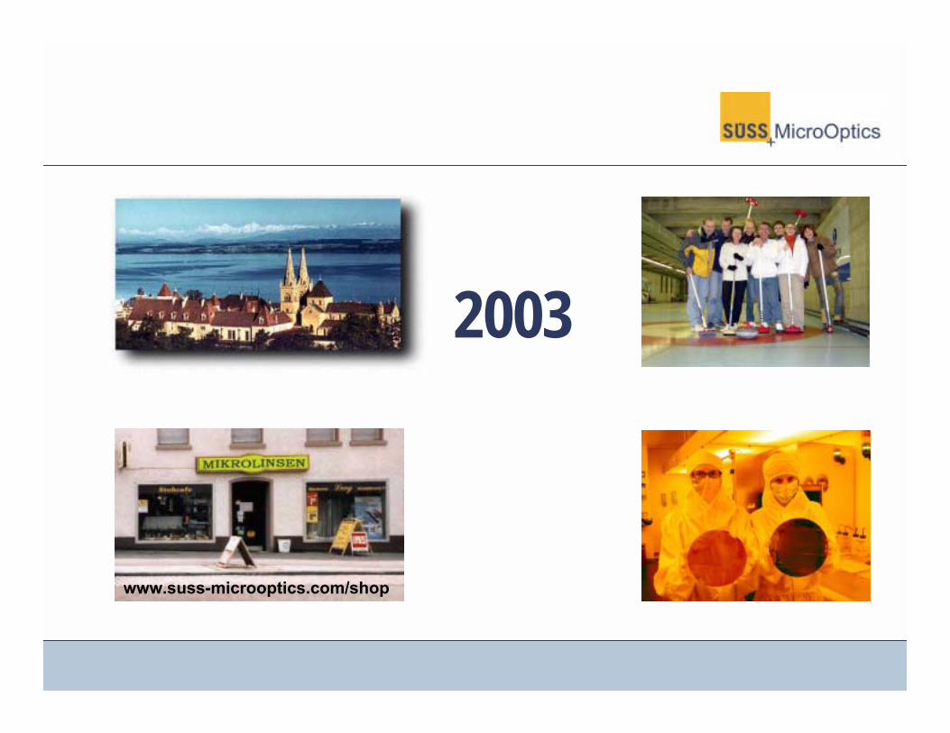
2003
www.suss-microoptics.com/shop


![Dynamic Plowing Lithography - TU Berlin€¦ · Das Rasterkraftmikroskop gehört zusammen mit seinem Vorgänger, dem Rastertunnelmikroskop (Scanning Tunneling Microscope, STM) [2]](https://img.pdfslide.org/doc/110x75/5f0727e57e708231d41b9580/dynamic-plowing-lithography-tu-berlin-das-rasterkraftmikroskop-gehrt-zusammen.jpg)