Embed Size (px)
Citation preview
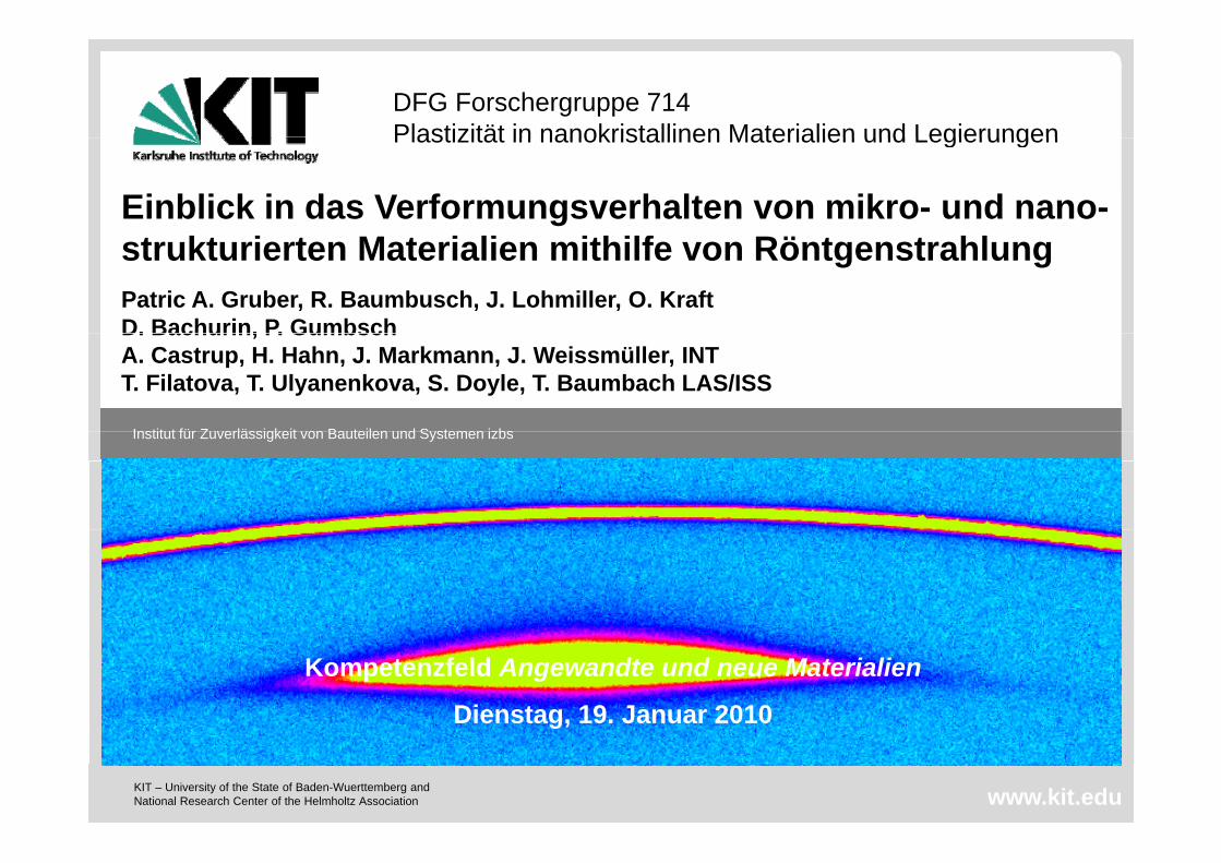
DFG Forschergruppe 714Plastizität in nanokristallinen Materialien und Legierungen
Einblick in das Verformungsverhalten von mikro- und nano-k i M i li i hilf Rö hl
Plastizität in nanokristallinen Materialien und Legierungen
strukturierten Materialien mithilfe von RöntgenstrahlungPatric A. Gruber, R. Baumbusch, J. Lohmiller, O. KraftD. Bachurin, P. Gumbsch
Institut für Zuverlässigkeit von Bauteilen und Systemen izbs
D. Bachurin, P. GumbschA. Castrup, H. Hahn, J. Markmann, J. Weissmüller, INTT. Filatova, T. Ulyanenkova, S. Doyle, T. Baumbach LAS/ISS
Institut für Zuverlässigkeit von Bauteilen und Systemen izbs
Kompetenzfeld Angewandte und neue Materialien
Dienstag, 19. Januar 2010
KIT – University of the State of Baden-Wuerttemberg and National Research Center of the Helmholtz Association www.kit.edu
g,
Outline
Mechanical testing and in situ characterization with XRD fXRD of
1. Thin metallic films on polyimide:
polycrystalline (columnar), single-crystalline, nanocrystalline
2 S ll l t lli i l t l2. Small scale metallic single crystals:
Microcolumns and nanowires
Determination of stress and strain
Characterization and identification of deformation mechanisms
Institut für Zuverlässigkeit von Bauteilen und Systemen2 20.01.2010
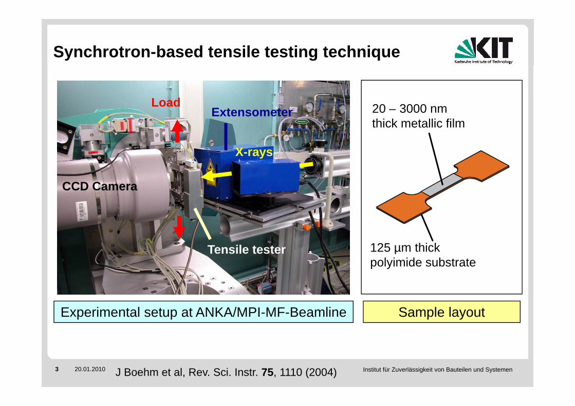
Synchrotron-based tensile testing technique
LoadExtensometer 20 – 3000 nm
X-rays
Extensometer 20 3000 nm thick metallic film
CCD Camera
y
Tensile tester 125 µm thickTensile tester 125 µm thick polyimide substrate
Experimental setup at ANKA/MPI-MF-Beamline Sample layout
Institut für Zuverlässigkeit von Bauteilen und Systemen3 20.01.2010 J Boehm et al, Rev. Sci. Instr. 75, 1110 (2004)
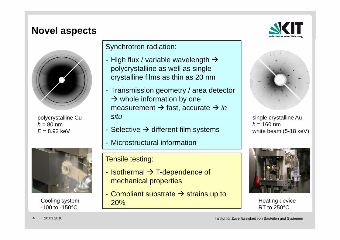
Novel aspects Synchrotron radiation:
- High flux / variable wavelength polycrystalline as well as single crystalline films as thin as 20 nm
- Transmission geometry / area detector g ywhole information by one
measurement fast, accurate in situpolycrystalline Cu single crystalline Au
- Selective different film systems
- Microstructural information
p y yh = 80 nmE = 8.92 keV
g yh = 160 nmwhite beam (5-18 keV)
Tensile testing:
- Isothermal T-dependence of Isothermal T dependence of mechanical properties
- Compliant substrate strains up to 20%Cooling system Heating device
Institut für Zuverlässigkeit von Bauteilen und Systemen4 20.01.2010
20%Cooling system -100 to -150°C
Heating device RT to 250°C
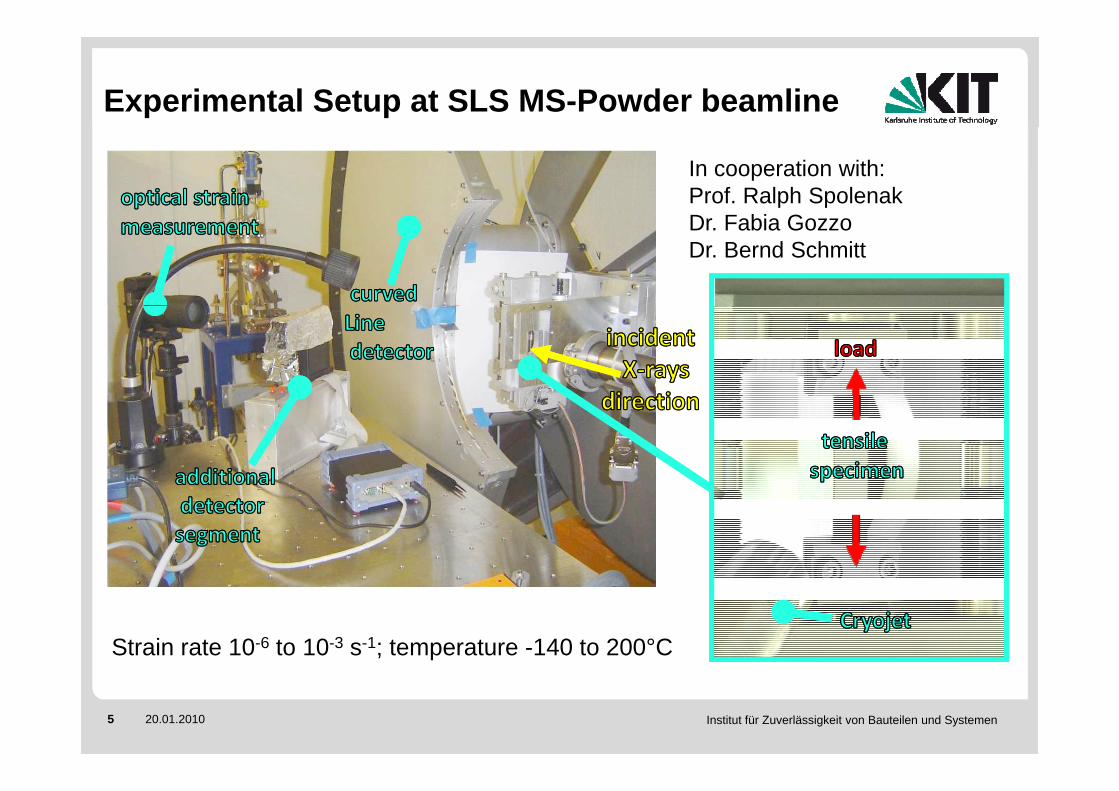
Experimental Setup at SLS MS-Powder beamline
In cooperation with:Prof. Ralph SpolenakD F bi GDr. Fabia GozzoDr. Bernd Schmitt
Strain rate 10-6 to 10-3 s-1; temperature -140 to 200°C
Institut für Zuverlässigkeit von Bauteilen und Systemen5 20.01.2010
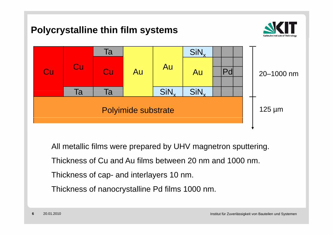
Polycrystalline thin film systems
C
Ta
A
SiNx
Cu Cu Au AuCu Au Pd
Ta Ta SiN SiN
20–1000 nm
Ta Ta SiNx SiNx
Polyimide substrate 125 µm
All t lli fil d b UHV t tt iAll metallic films were prepared by UHV magnetron sputtering.
Thickness of Cu and Au films between 20 nm and 1000 nm.
Thickness of cap- and interlayers 10 nm.
Thickness of nanocrystalline Pd films 1000 nm.
Institut für Zuverlässigkeit von Bauteilen und Systemen6 20.01.2010
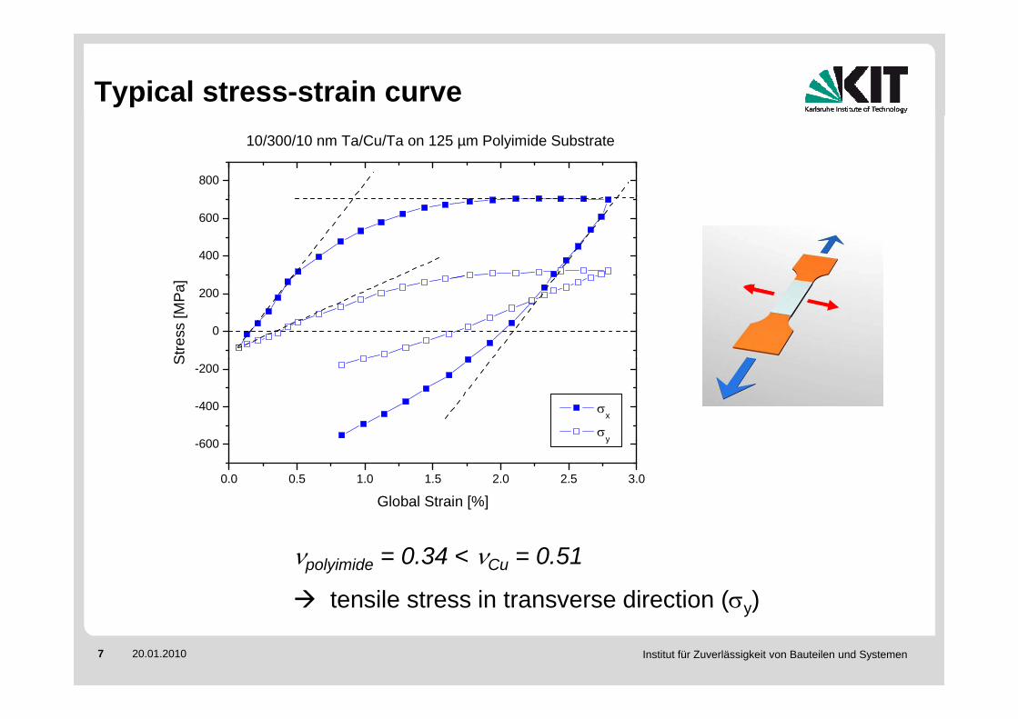
Typical stress-strain curve
800
10/300/10 nm Ta/Cu/Ta on 125 µm Polyimide Substrate
400
600
0
200
Stre
ss [M
Pa]
600
-400
-200
σx
σy
S
0.0 0.5 1.0 1.5 2.0 2.5 3.0
-600 y
Global Strain [%]
νpolyimide = 0.34 < νCu = 0.51
tensile stress in transverse direction (σ )
Institut für Zuverlässigkeit von Bauteilen und Systemen7 20.01.2010
tensile stress in transverse direction (σy)
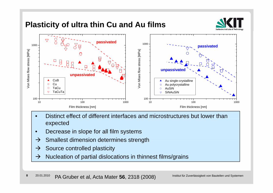
Plasticity of ultra thin Cu and Au films
1000
Pa]
passivated 1000
Pa]
passivated
s flo
w s
tress
[MP
unpassivated
s flo
w s
tress
[MP
unpassivated
CuB Cu TaCu TaCuTa
Von
Mis
es unpassivated Au single-crystalline Au polycrystalline AuSiN SiNAuSiN
Von
Mis
es
10 100 1000100
Film thickness [nm]10 100 1000
100
Film thickness [nm]
• Distinct effect of different interfaces and microstructures but lower than expected
• Decrease in slope for all film systemsSmallest dimension determines strengthSmallest dimension determines strengthSource controlled plasticityNucleation of partial dislocations in thinnest films/grains
Institut für Zuverlässigkeit von Bauteilen und Systemen8 20.01.2010 PA Gruber et al, Acta Mater 56, 2318 (2008)
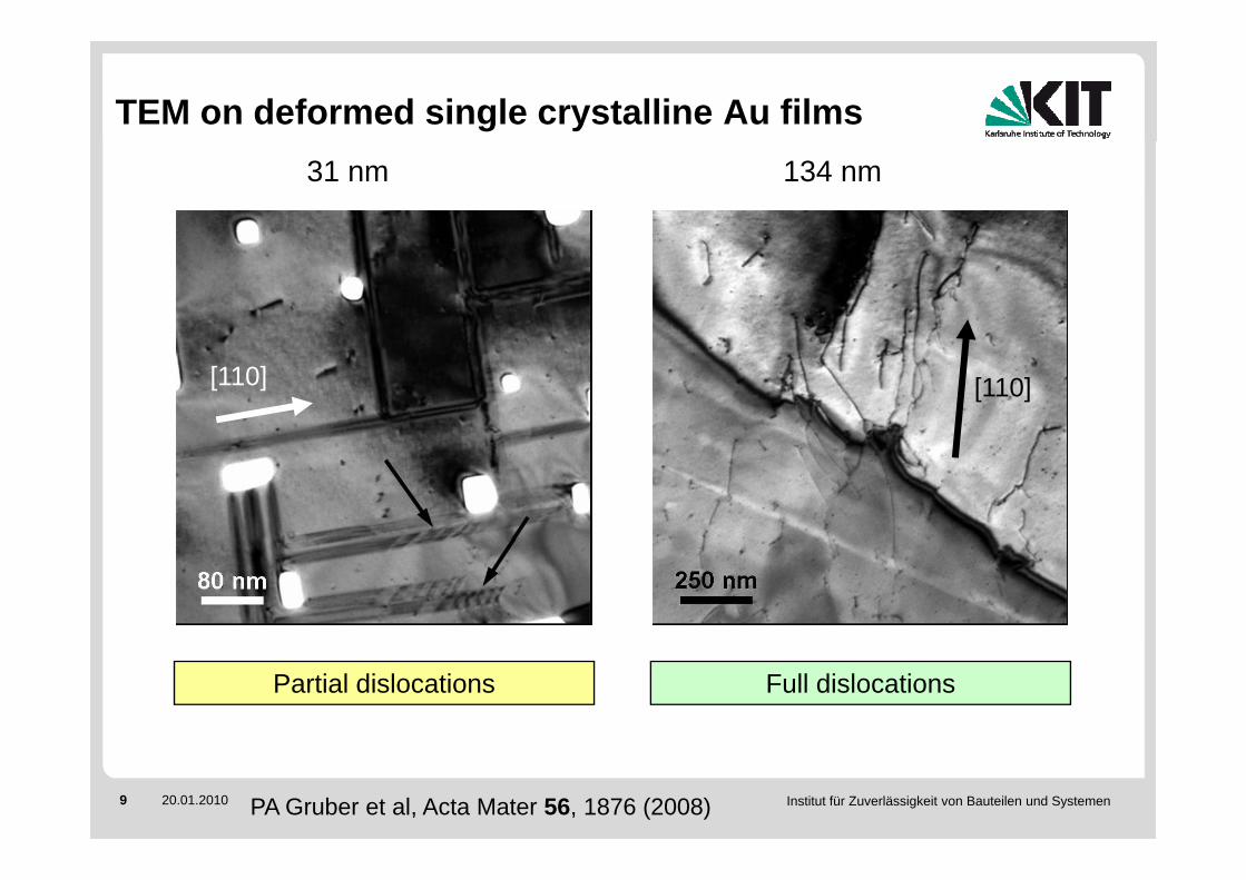
TEM on deformed single crystalline Au films31 nm 134 nm
[110][110]
Partial dislocations Full dislocations
Institut für Zuverlässigkeit von Bauteilen und Systemen9 20.01.2010 PA Gruber et al, Acta Mater 56, 1876 (2008)
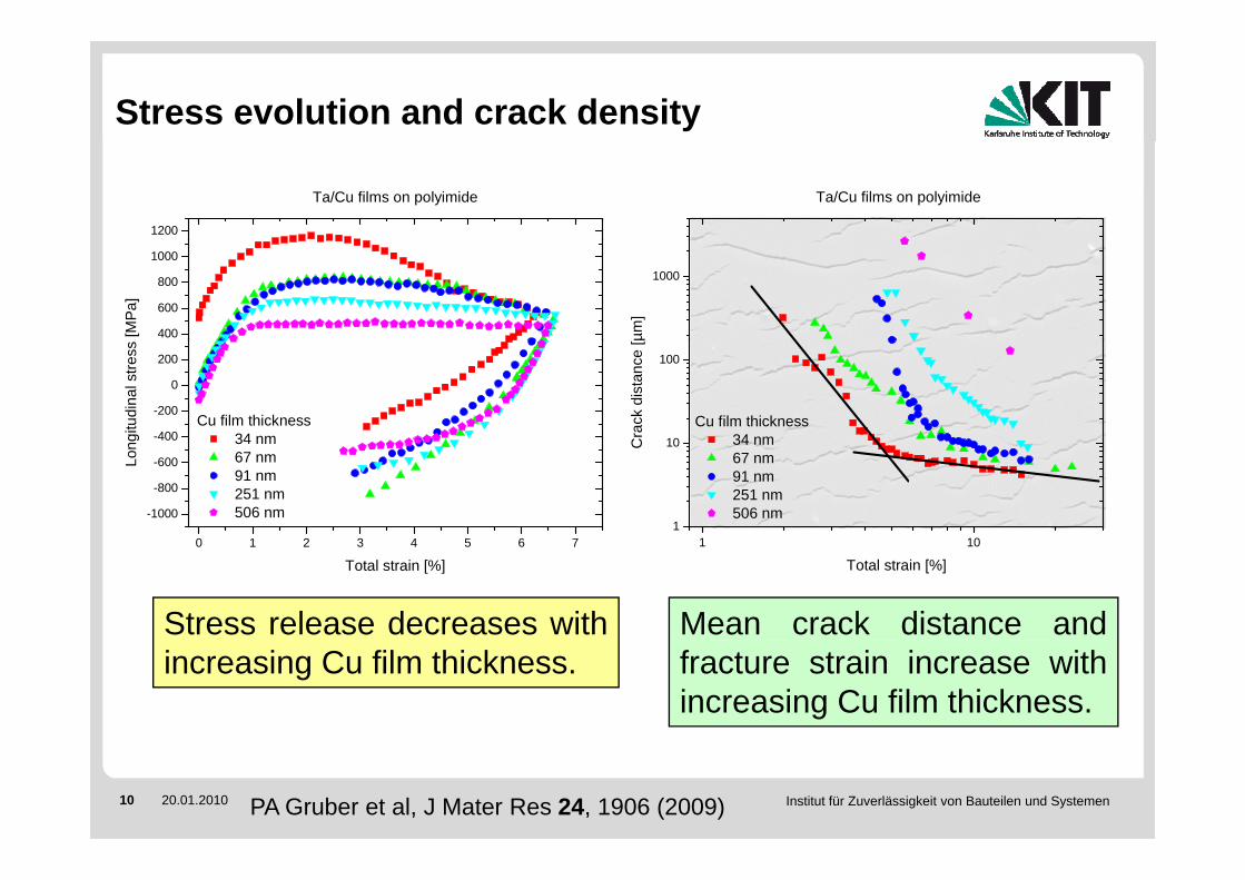
Stress evolution and crack density
Ta/Cu films on polyimide
1200
Ta/Cu films on polyimide
1000
µm]
400
600
800
1000
[MPa
]
10
100
Cu film thickness34 nm
Cra
ck d
ista
nce
[
-400
-200
0
200
gitu
dina
l stre
ss
Cu film thickness34 nm
1 101
10 34 nm 67 nm 91 nm 251 nm 506 nm
C
0 1 2 3 4 5 6 7
-1000
-800
-600
400
Long 34 nm
67 nm 91 nm 251 nm 506 nm
1 10
Total strain [%]0 1 2 3 4 5 6 7
Total strain [%]
Stress release decreases with Mean crack distance andincreasing Cu film thickness. fracture strain increase with
increasing Cu film thickness.
Institut für Zuverlässigkeit von Bauteilen und Systemen10 20.01.2010 PA Gruber et al, J Mater Res 24, 1906 (2009)
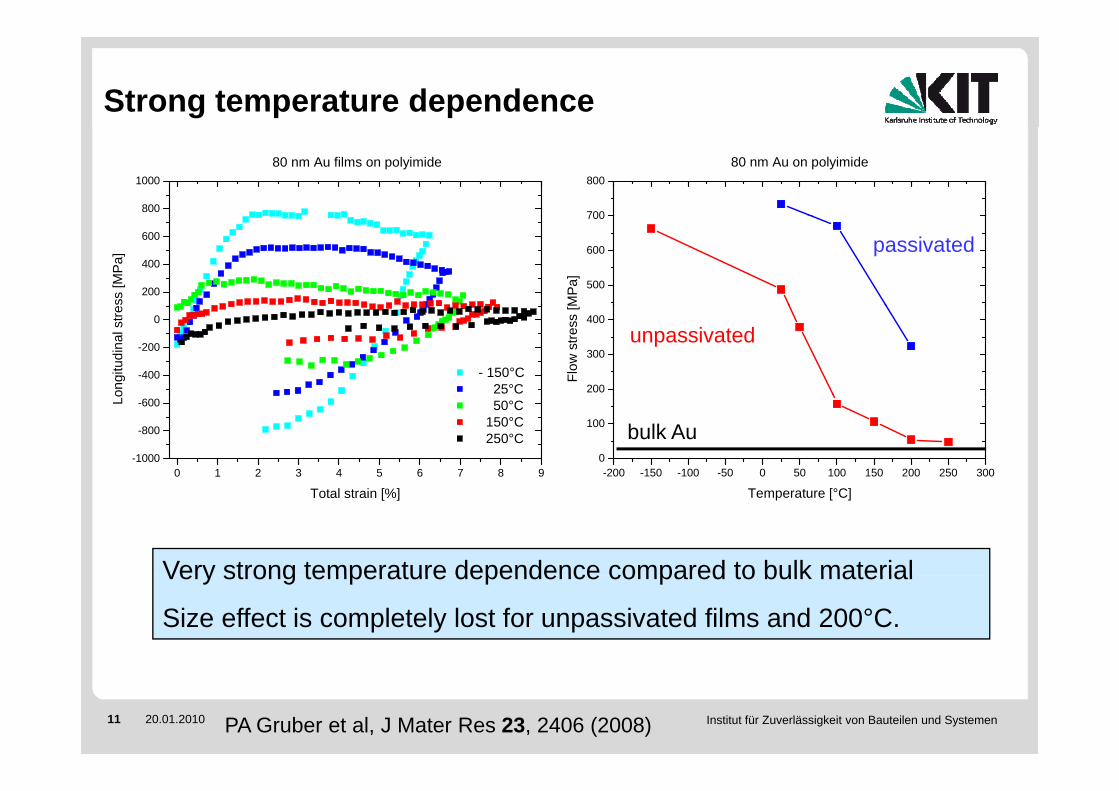
Strong temperature dependence
800
1000 80 nm Au films on polyimide
700
80080 nm Au on polyimide
200
400
600
ss [M
Pa]
500
600
700
MPa
]
passivated
-400
-200
0
- 150°C 25°C
ongi
tudi
nal s
tre
200
300
400
Flow
stre
ss [
unpassivated
0 1 2 3 4 5 6 7 8 9-1000
-800
-600 50°C 150°C 250°C
Lo
-200 -150 -100 -50 0 50 100 150 200 250 3000
100 bulk Au
Total strain [%] Temperature [°C]
Very strong temperature dependence compared to bulk materialVery strong temperature dependence compared to bulk material
Size effect is completely lost for unpassivated films and 200°C.
Institut für Zuverlässigkeit von Bauteilen und Systemen11 20.01.2010 PA Gruber et al, J Mater Res 23, 2406 (2008)
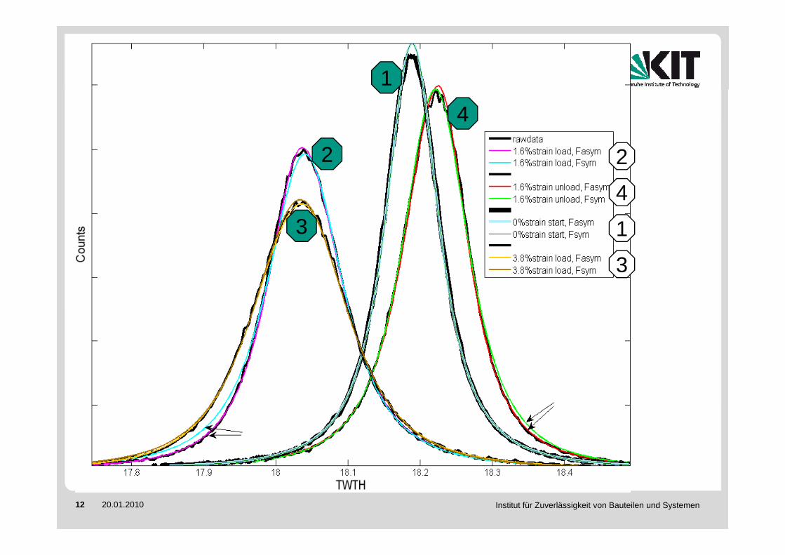
1
2
4
22 2
43 1
3
Institut für Zuverlässigkeit von Bauteilen und Systemen12 20.01.2010
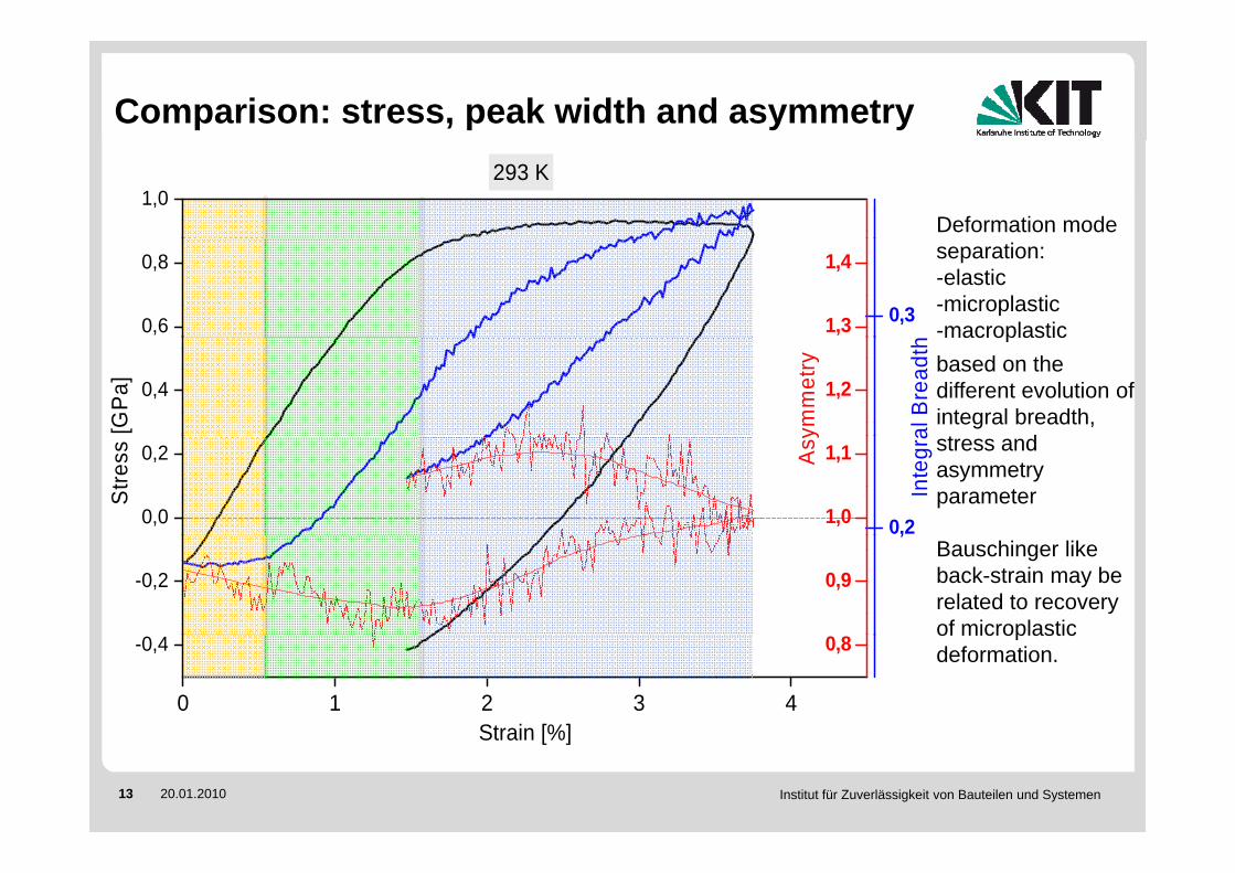
Comparison: stress, peak width and asymmetry
1,0293 K
Deformation mode
0,6
0,8
0,31,3
1,4 separation:-elastic-microplastic-macroplastic
0,4
[GP
a]
al B
read
th
1,2
ymm
etry
macroplasticbased on the different evolution of integral breadth, t d
0,0
0,2
Stre
ss
0,2
Inte
gra
1,0
1,1 Asy stress and
asymmetry parameter
-0,2
,
0,9Bauschinger like back-strain may be related to recovery of microplastic
0 1 2 3 4
-0,4
Strain [%]
0,8of microplasticdeformation.
Institut für Zuverlässigkeit von Bauteilen und Systemen13 20.01.2010
Strain [%]
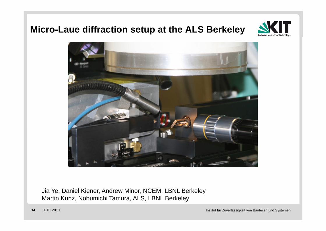
Micro-Laue diffraction setup at the ALS Berkeley
Jia Ye, Daniel Kiener, Andrew Minor, NCEM, LBNL Berkeley
Institut für Zuverlässigkeit von Bauteilen und Systemen14 20.01.2010
yMartin Kunz, Nobumichi Tamura, ALS, LBNL Berkeley
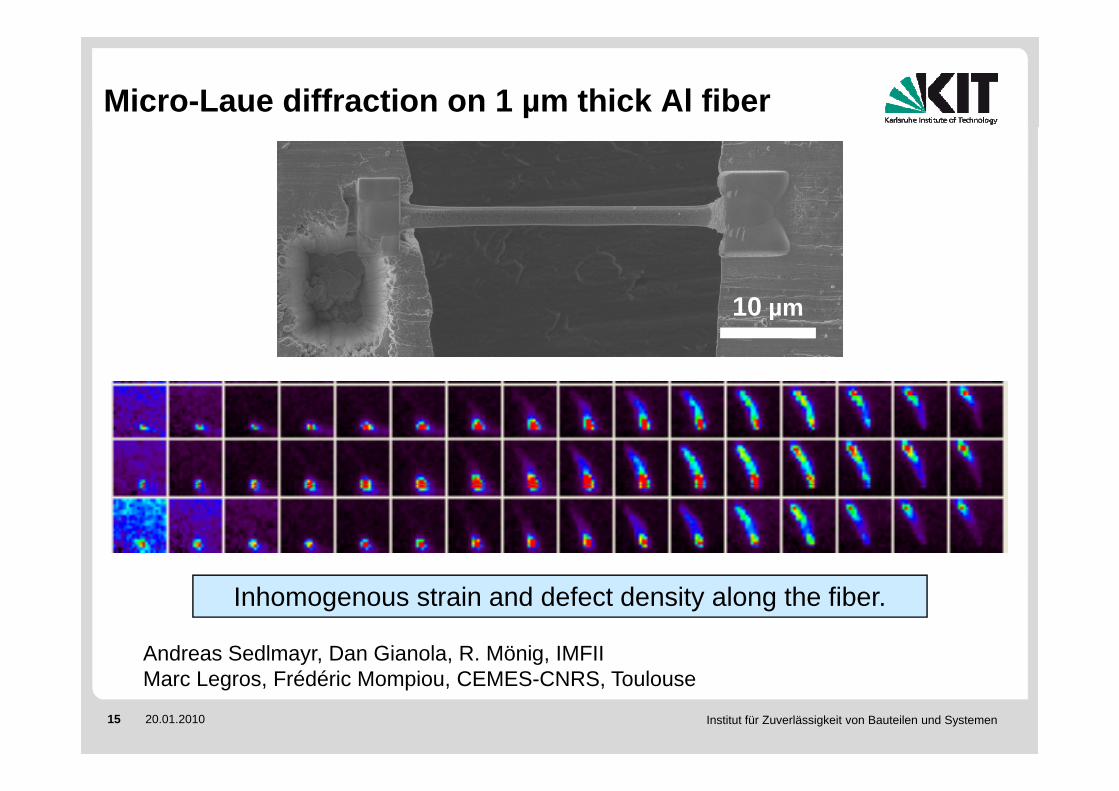
Micro-Laue diffraction on 1 µm thick Al fiber
10 µm10 µm
Inhomogenous strain and defect density along the fiber.
Andreas Sedlmayr, Dan Gianola, R. Mönig, IMFII
Institut für Zuverlässigkeit von Bauteilen und Systemen15 20.01.2010
y gMarc Legros, Frédéric Mompiou, CEMES-CNRS, Toulouse
Summary
In situ synchrotron setups for mechanical testing of thin films and micro- and y p gnanostructures are available.
Size effects on flow stress and deformation behavior can be investigated for thin films and micro and nanocrystalsthin films and micro- and nanocrystals.
Combination of stress determination and peak shape analysis enables characterization of elastic, microplastic and macroplastic deformation.p p
Micro-Laue diffraction yields local information on strain and defect densities within single grains or across micro- and nanostructures.
Institut für Zuverlässigkeit von Bauteilen und Systemen16 20.01.2010
![Mikro- und Nano-Spektroskopie und Detektor- charakterisierung im IR- und THz … · schaften, Biologie oder Medizin [2–4]. Die PTB hat an den Speicherringen BESSY I und II mehr](https://img.pdfslide.org/doc/110x75/5e7c1ba8f92c7262da021be8/mikro-und-nano-spektroskopie-und-detektor-charakterisierung-im-ir-und-thz-schaften.jpg)