Embed Size (px)
Citation preview
Florian Beschliesser, BSc
FPGA-based verification of a
narrowband receiver
zur Erlangung des akademischen Grades
MASTERARBEIT
Masterstudium Elektrotechnik-Wirtschaft
eingereicht an der
Technischen Universität Graz
Ao.Univ.-Prof. Dr. Erich Leitgeb
Betreuer
Institut für Hochfrequenztechnik
Mitbetreuer
Dr. Martin Gossar (NXP Semiconductors GmbH)
Graz, Mai 2014
Diplom-Ingenieur
EIDESSTATTLICHE ERKLÄRUNG
AFFIDAVIT
Ich erkläre an Eides statt, dass ich die vorliegende Arbeit selbstständig verfasst,
andere als die angegebenen Quellen/Hilfsmittel nicht benutzt, und die den benutzten
Quellen wörtlich und inhaltlich entnommenen Stellen als solche kenntlich gemacht
habe. Das in TUGRAZonline hochgeladene Textdokument ist mit der vorliegenden
Masterarbeit identisch.
I declare that I have authored this thesis independently, that I have not used other
than the declared sources/resources, and that I have explicitly indicated all material
which has been quoted either literally or by content from the sources used. The text
document uploaded to TUGRAZonline is identical to the present master‘s thesis.
Datum / Date Unterschrift / Signature

Diplomarbeit
FPGA-based verification of a
narrowband receiver
Florian Beschliesser
Institut für Hochfrequenztechnik
Technische Universität Graz
Leiter: Univ.-Prof. Dr. Wolfgang Bösch
In Kooperation mit
NXP Semiconductors GmbH
Betreuer: Ao.Univ.-Prof. Dr. Erich Leitgeb
Mitbetreuer: Dr. Martin Gossar (NXP) Graz, im Mai 14
Graz, May 2014 Page 1
Abstract
This work was created in co-operation with the company NXP Austria GmbH and
contains a FPGA based verification of a narrowband receiver using an analog
frontend IC to gather the input ADC stream and a FPGA-evaluation board emulating
the digital receive chain under test.
These verification setup should increase the test coverage of the prototypes before
they are released for production. Furthermore the intense simulation time could be
mitigated by using such a FPGA-based system.
Introductorily, the theoretical background of this thesis is discussed in detail. This
chapter is split into two main parts: The analog frontend and the digital receive chain.
Afterwards the necessary hardware is introduced via block diagrams and detailed
descriptions.
In addition the software environment and the TestStation project where this project
should be integrated is introduced. In doing so, typical fields of application and
potential users are discussed.
Finally the implementation is described in detail and the results are shown. Also a
forecast of the portability of NXP products and applications in the future is given.

Graz, May 2014 Page 2
Kurzfassung
Diese Arbeit wurde in Kooperation mit der Firma NXP Austria GmbH erstellt und
enthält eine FPGA-basierte Verifikation eines Schmalbandempfängers. Umgesetzt
wurde das Projekt mit einem analogen Frontend-IC, um den ADC Strom zu
erzeugen, und einer FPGA – Evaluierungsplatine welche die zu testende digitale
Empfangskette emuliert.
Dieses Verifikationssetup soll die Testabdeckung der Prototypen erhöhen, bevor sie
für die Produktion freigegeben werden. Weiters könnte die intensive Simulationszeit
durch Verwendung eines solchen FPGA-basierten Systems gemildert werden.
Einleitend wird der theoretische Hintergrund dieser Arbeit ausführlich diskutiert.
Dieses Kapitel ist in zwei Hauptteile aufgeteilt: Das analoge Frontend und die digitale
Empfangskette.
Danach wird die notwendige Hardware anhand von Blockdiagrammen und
detaillierten Beschreibungen vorgestellt.
Außerdem wird die Softwareumgebung und das TestStation Projekt vorgestellt, in
jene das Projekt integriert werden soll. Dabei werden mögliche Einsatzbereiche und
potentielle Anwender diskutiert.
Anschließend wird auf die Umsetzung genauer eingegangen, das Finale Ergebnis
vorgestellt sowie ein Ausblick auf die Portierbarkeit auf neue Produkte und zukünftige
Einsatzbereiche gegeben.
Graz, May 2014 Page 3
Table of Contents
1. Motivation and aim of the study ........................................................................... 6
2. Technical background .......................................................................................... 9
2.1 Analog front end ............................................................................................ 9
2.1.1 Low noise amplifier (LNA) ..................................................................... 10
2.1.2 Attenuators ............................................................................................ 11
2.1.3 Mixer ..................................................................................................... 11
2.1.4 Baseband amplifier (TIA) ...................................................................... 12
2.1.5 Automatic gain control (AGC) ............................................................... 13
2.1.6 Sigma delta ADC .................................................................................. 13
2.2 Digital IF preprocessing ............................................................................... 14
2.2.1 Decimation filter .................................................................................... 15
2.2.2 DC notch filter ....................................................................................... 16
2.2.3 IQ mismatch compensation................................................................... 17
2.3 Narrowband receive chain ........................................................................... 17
2.3.1 Channel mixer ....................................................................................... 18
2.3.2 Channel filter ......................................................................................... 19
2.3.3 Demodulator ......................................................................................... 22
2.3.4 Clock data recovery .............................................................................. 23
2.3.5 Data processing .................................................................................... 26
2.4 Micro controller MRK3 ................................................................................. 28
2.4.1 Functional description ........................................................................... 28
2.4.2 Monitor and download interface ............................................................ 29
3. Measurement procedures and standards........................................................... 31
3.1 Receiver sensitivity ...................................................................................... 32
3.1.1 Method of measurement with continuous bit streams ........................... 32
3.1.2 Method of measurement with messages .............................................. 33
3.2 Receiver jammer performance .................................................................... 35
3.2.1 Adjacent channel rejection .................................................................... 36
Graz, May 2014 Page 4
3.2.2 Co-channel rejection ............................................................................. 37
3.2.3 Image rejection ratio ............................................................................. 38
3.2.4 Image channel rejection ........................................................................ 39
3.2.5 Blocking ................................................................................................ 39
3.2.5 Spurious response rejection.................................................................. 40
3.3 Modulation techniques ................................................................................. 41
3.3.1 Frequency Shift Keying (FSK) ............................................................... 41
3.3.2 Amplitude Shift Keying (ASK) ............................................................... 42
4. Implementation .................................................................................................. 43
4.1 FPGA - Field Programmable Gate Array ..................................................... 43
4.1.1 Functional description ........................................................................... 44
4.1.2 Hardware structure ............................................................................... 44
4.1.3 Design and synthesis ............................................................................ 45
4.1.4 Motivation for FPGA verification ............................................................ 46
4.1.5 Strengths............................................................................................... 47
4.1.6 Weaknesses and limitations.................................................................. 48
4.1.7 Implementation effort ............................................................................ 49
4.2 Hardware setup ........................................................................................... 52
4.2.1 Analog frontend ..................................................................................... 53
4.2.2 Level shifter board ................................................................................ 54
4.2.3 FPGA evaluation board ......................................................................... 55
4.2.4 Signal generator .................................................................................... 56
4.2.5 Communication and modulation tool “TestStation” ............................... 58
4.3 Environmental software ............................................................................... 60
4.3.1 TestStation firmware ............................................................................. 61
4.3.2 Host software environment ................................................................... 62
4.3.3 Frontend IC firmware ............................................................................ 63
4.3.4 Backend IC Firmware ........................................................................... 64
4.4 Host software............................................................................................... 64
4.4.1 Frame error rate measurement ............................................................. 65
Graz, May 2014 Page 5
4.4.2 Sensitivity measurement ....................................................................... 66
4.4.3 Sensitivity test case .............................................................................. 67
4.4.4 Enhanced sensitivity test case implementation ..................................... 69
4.4.5 Signal to jammer ratio measurement .................................................... 70
4.4.6 Interferer performance test case ........................................................... 70
5. Results ............................................................................................................... 73
5.1 Hardware setup ........................................................................................... 73
5.2 Configuration files ........................................................................................ 74
5.2.1 Sensitivity measurements ..................................................................... 75
5.2.2 Jammer measurements ........................................................................ 75
5.3 Result files ................................................................................................... 76
5.3.1 Sensitivity measurements ..................................................................... 76
5.3.2 Jammer measurements ........................................................................ 76
5.4 Result viewer ............................................................................................... 76
5.4.1 Sensitivity measurements ..................................................................... 77
5.4.2 Enhanced sensitivity measurements ..................................................... 77
5.4.3 Jammer measurements ........................................................................ 78
5.5 Excel export ................................................................................................. 79
5.5.1 Sensitivity measurements ..................................................................... 79
5.5.2 Jammer measurements ........................................................................ 80
6. Conclusion and outlook ...................................................................................... 82
6.1 Comparison FPGA / IC ................................................................................ 82
6.2 Capturing of ADC streams ........................................................................... 83
6.3 Measurement time optimizations ................................................................. 83
6.4 Portability to future prototypes ..................................................................... 84
References ............................................................................................................... 85
List of Figures ........................................................................................................... 87
List of Tables ............................................................................................................ 90
Appendix A – RF frontend evaluation board ............................................................. 91
Appendix B – FPGA evaluation board ...................................................................... 92
Graz, May 2014 Page 6
1. Motivation and aim of the study
NXP Semiconductors Austria GmbH develops receiver systems since more than 10
years. Its main customers are placed in the automotive industry, such as Continental
or Bosch. The main applications are car opening and immobilizing systems, where
NXP provides several one-chip solutions for the key side, as well as for the car side.
This means one single chip includes all the functionality for the application, no further
microcontrollers or power amplifiers are needed.
The design of such receivers is split into two main parts: the analog front end and the
digital back end. Both parts are essential for the performance of the final product and
therefore big teams are working on each sub-block.
The analog design process is nearly the same since years. Taking the rough idea of
a block as a starting point, first a schematic has to be developed. Afterwards an
extensive and detailed simulation of all functions of the designed block has to be
performed. Depending on the results, changes have to be done in the schematic and
the simulation needs to be repeated again. Finally, if the results are looking fine,
there are additional simulations over process and application corners performed,
which should exclude the malfunction of this block under extreme conditions (e.g.
extreme temperatures). Next to that, the analog layout of this block is drawn. The
block design is finished, if the layout versus schematic simulation was pass. This
simulation should detect possible function or parameter changes of the block caused
by the layout. Like said before, this process is nearly unchanged since years. But this
does not mean that the quality did not increase since years! The tools used for
designing, simulating and layouting are improved periodically. The simulation results
are more detailed, the simulation time gets less, displaying and reviewing the results
is easier, etc. Therefore the design tools help the developers to work more efficient
and produce high quality output.
Looking at the digital design process 10 years ago, more changes and innovations
are visible nowadays. At least one thing did not change much: The Verilog or VHDL
code is still typed into fancy editors most likely on an UNIX workstation. Maybe some
intelligent code auto-completion system was introduced by some of the tools but in
principal the way of working in the design phase is unchanged since years. Most of
the innovations were happening in the digital design verification process. The main

Graz, May 2014 Page 7
verification solution is of course the digital simulation. Designing a test bench for a
new digital block of the IC can require more working time than the design of the
digital block itself. Nevertheless such a test bench is needed for every sub-block of
the digital backend to prove its correct functionality. A digital block is called verified, if
all possible input signal combinations were applied by the test bench. Each input
signal combination should result in a certain output signal combination, the test
bench should automatically compare the expected output with the simulated output
and report possible errors. Exactly at this point one essential problem pops up: How
does the verification look like, if the number of possible input signal combination is
infinite, such as for the input of a receiver? How would you verify these blocks?
Looking at NXP Semiconductors, one possible answer to the question above is to
introduce default use cases and a so called reference frame, which is an example of
a modulated input signal fed into the digital receiver. All the simulations are done with
this reference frame for all use cases. The use case defines the modulation
technique, the modulation index and the chip rate of the input signal. The reference
frame defines the encoding and the amount of the sent data. As you can imagine, the
simulation coverage is quite low if you are just using one input frame and some chip
rate / modulation index combinations. Unfortunately the simulation time is very high
for such test benches, therefore the simulation coverage can’t be increased easily.
This limitation is also limiting the quality of the design itself, because a solid
verification is the key to success in such design projects.
Considering the limitations of the simulation process above, there was a request for a
faster, more effective way of verifying the digital sub-blocks of the receiver. A new
idea, and also the topic of this study was born: FPGA Verification.
Aim of this study is to implement an automated test bench using an UHF transmitter,
an analog front end and a field programmable gate array (FPGA) which is an
integrated circuit that can be configured after manufacturing by the end customer. It
contains the digital blocks of the receiver to increase the test coverage of the digital
design. Not only one, but dozens of different input frames, using several use cases
and modulation techniques should be tested. Additionally the test bench should
provide functionality to simulate a second present transmitter in the working area of
the receiver, meaning the interferer performance of the design. Very important is, that
Graz, May 2014 Page 8
the test bench is easily configurable, portable to any version of the digital receiver
and able to produce well-structured result tables and plots.
Graz, May 2014 Page 9
2. Technical background
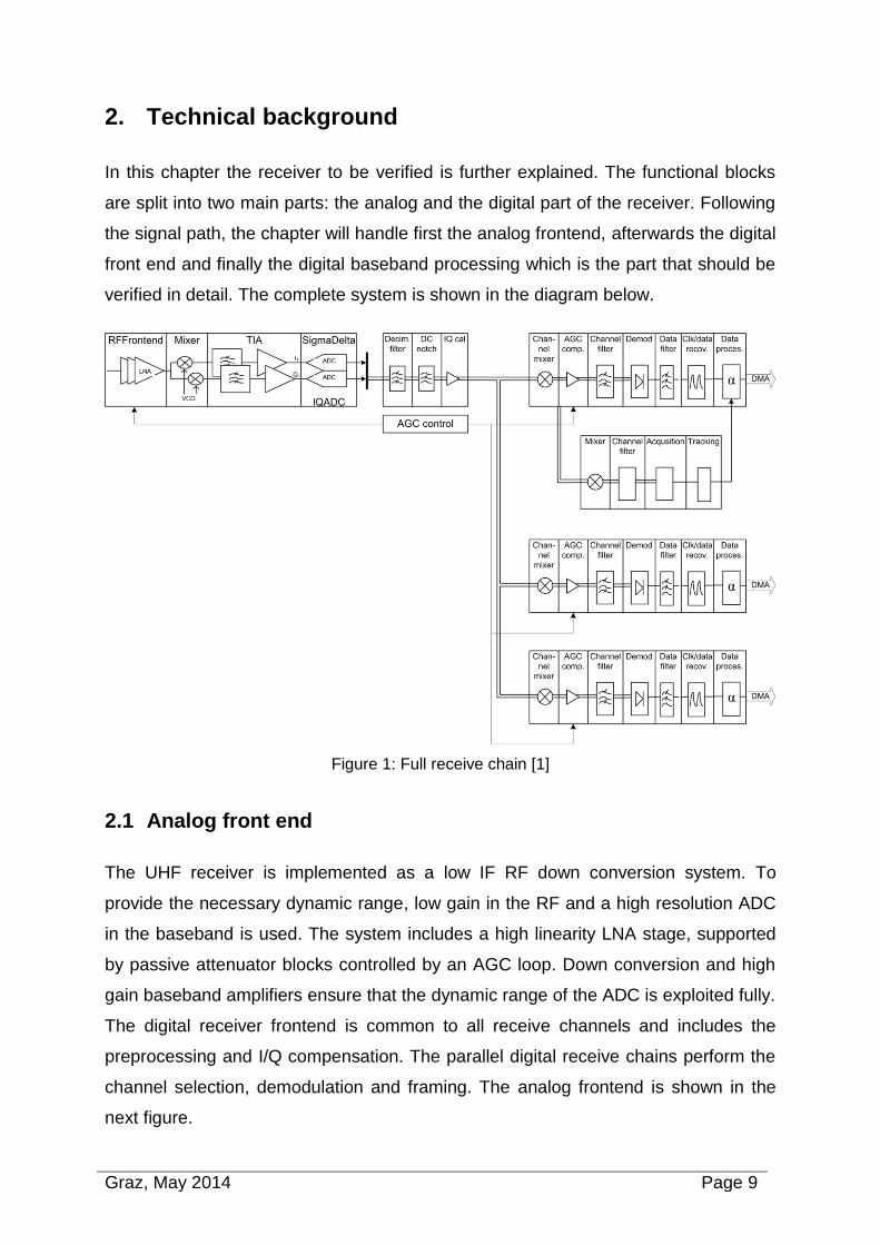
In this chapter the receiver to be verified is further explained. The functional blocks
are split into two main parts: the analog and the digital part of the receiver. Following
the signal path, the chapter will handle first the analog frontend, afterwards the digital
front end and finally the digital baseband processing which is the part that should be
verified in detail. The complete system is shown in the diagram below.
Figure 1: Full receive chain [1]
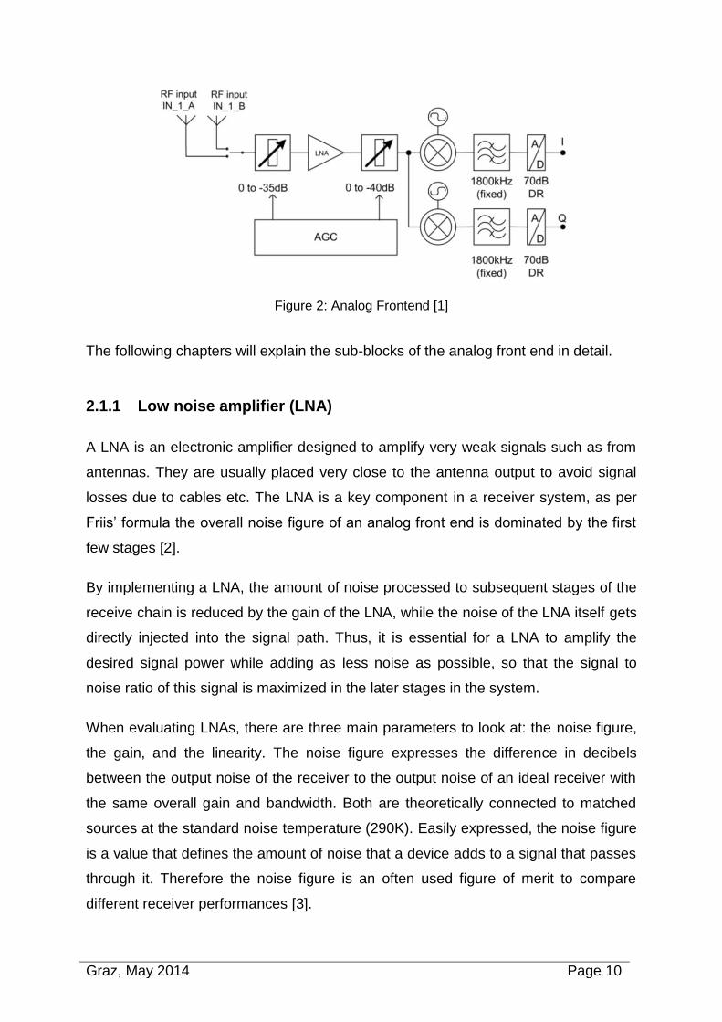
2.1 Analog front end
The UHF receiver is implemented as a low IF RF down conversion system. To
provide the necessary dynamic range, low gain in the RF and a high resolution ADC
in the baseband is used. The system includes a high linearity LNA stage, supported
by passive attenuator blocks controlled by an AGC loop. Down conversion and high
gain baseband amplifiers ensure that the dynamic range of the ADC is exploited fully.
The digital receiver frontend is common to all receive channels and includes the
preprocessing and I/Q compensation. The parallel digital receive chains perform the
channel selection, demodulation and framing. The analog frontend is shown in the
next figure.
Graz, May 2014 Page 10
Figure 2: Analog Frontend [1]
The following chapters will explain the sub-blocks of the analog front end in detail.
2.1.1 Low noise amplifier (LNA)
A LNA is an electronic amplifier designed to amplify very weak signals such as from
antennas. They are usually placed very close to the antenna output to avoid signal
losses due to cables etc. The LNA is a key component in a receiver system, as per
Friis’ formula the overall noise figure of an analog front end is dominated by the first
few stages [2].
By implementing a LNA, the amount of noise processed to subsequent stages of the
receive chain is reduced by the gain of the LNA, while the noise of the LNA itself gets
directly injected into the signal path. Thus, it is essential for a LNA to amplify the
desired signal power while adding as less noise as possible, so that the signal to
noise ratio of this signal is maximized in the later stages in the system.
When evaluating LNAs, there are three main parameters to look at: the noise figure,
the gain, and the linearity. The noise figure expresses the difference in decibels
between the output noise of the receiver to the output noise of an ideal receiver with
the same overall gain and bandwidth. Both are theoretically connected to matched
sources at the standard noise temperature (290K). Easily expressed, the noise figure
is a value that defines the amount of noise that a device adds to a signal that passes
through it. Therefore the noise figure is an often used figure of merit to compare
different receiver performances [3].
Graz, May 2014 Page 11
The implemented LNA is a wideband inductor-free, highly-linear, low-power and low-
noise amplifier. It uses internal feedback for obtaining its high linearity and a well-
defined gain as well as good input matching over temperature and voltage. The LNA
has a single-ended input with a wide-band input matching optimized for 200 Ohms.
2.1.2 Attenuators
Passive 2 dB step attenuators are positioned in front of the LNA and in front of the
mixer in order to control the gain of the receiver. The input selection between the two
antenna inputs is realized by the first attenuator. The radio frequency (RF) inputs
have integrated electrostatic discharge (ESD) protection and integrated alternating
current (AC) coupling for easy application. A matching network can be applied off-
chip for best performance and adaptation to different source impedances.
2.1.3 Mixer
The implemented mixer is an IQ mixer. It addresses the problem of maximum
information density in a limited bandwidth by allowing the user to modulate both the
in-phase and quadrature components of a carrier simultaneously. The basic building
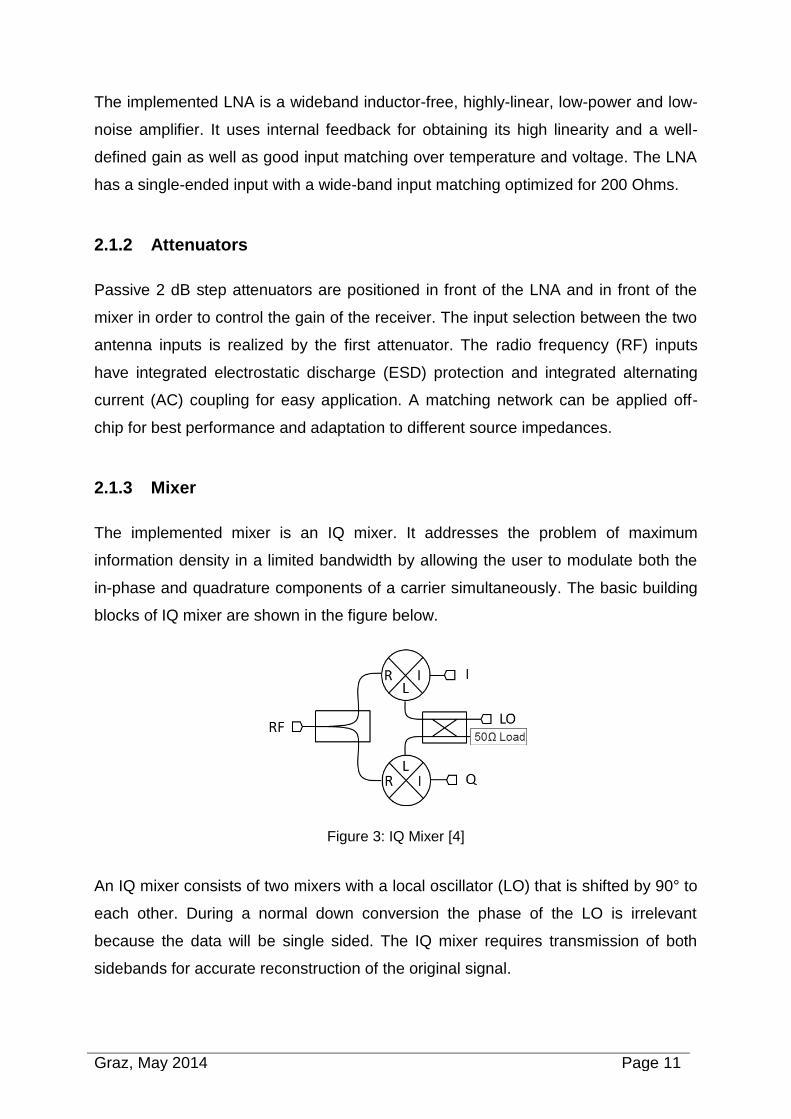
blocks of IQ mixer are shown in the figure below.
Figure 3: IQ Mixer [4]
An IQ mixer consists of two mixers with a local oscillator (LO) that is shifted by 90° to
each other. During a normal down conversion the phase of the LO is irrelevant
because the data will be single sided. The IQ mixer requires transmission of both
sidebands for accurate reconstruction of the original signal.
Graz, May 2014 Page 12
The IQ mixer uses the basis of quadrature modulation, meaning it can be used to
cancel out one of the two side bands, the image channel. By adding an extra 90°
phase shift to the Q channel after mixing, a complete 180° phase shift will be created,
leading to the inversion of one of the original signal components. Adding the two
mixer output channel would now result in a cancellation of one component of the
signal, while the other component is reinforced. This is called image rejection [4].
When an IQ mixer is used as a down-converter it allows both of the original data
signals to be retrieved with an appropriately phased LO signal. The image channel is
finally removed in the digital channel filter. A special algorithm is used to remove the
impact of analog mismatch in the I and Q mixer on the image rejection, what normally
would cause the intrusion of the image channel into the wanted channel.
2.1.4 Baseband amplifier (TIA)
The baseband amplifier stage amplifies the balanced quadrature (I and Q) mixer
output signals to the optimal level for the analog to digital converter (ADC) and
performs the anti-aliasing filtering in front of the sigma-delta ADC. Internal DC offset
correction loops guarantees maximum image suppression and high linearity /
dynamic range.
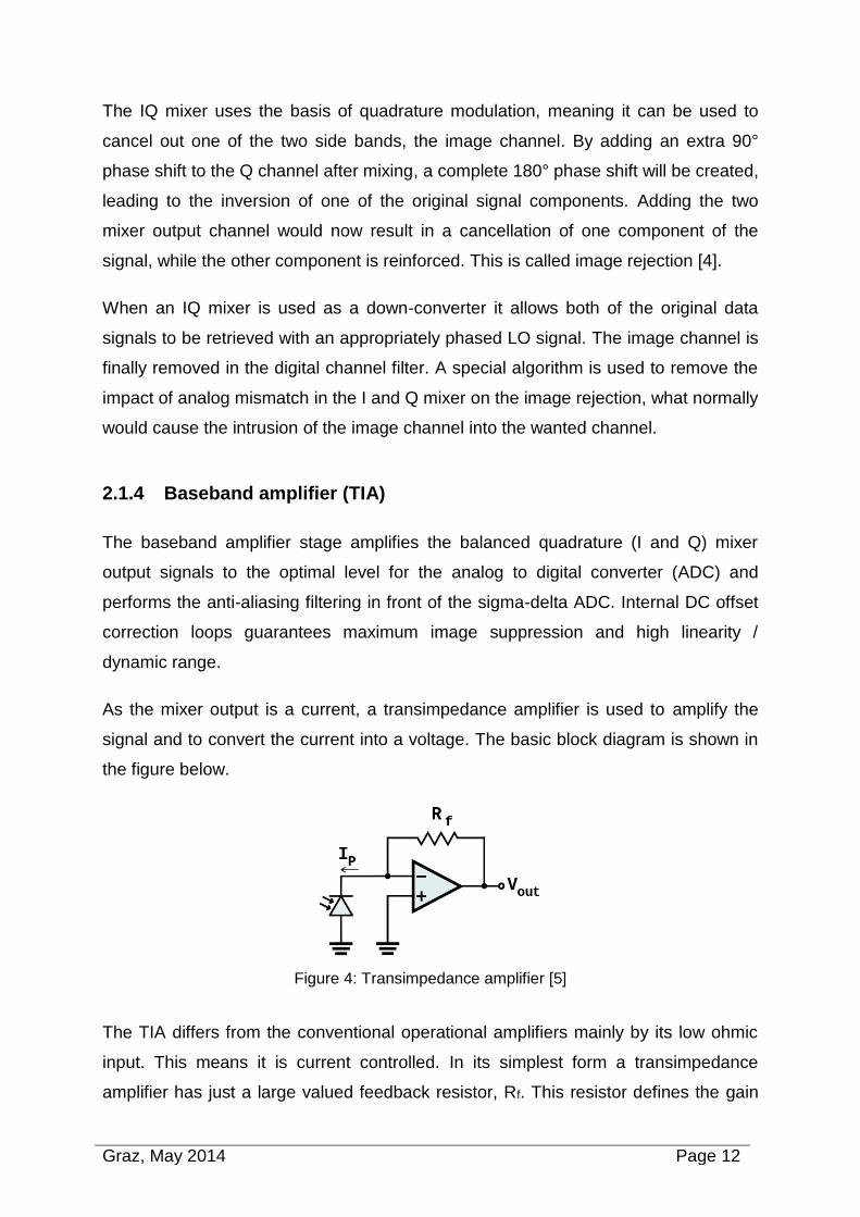
As the mixer output is a current, a transimpedance amplifier is used to amplify the
signal and to convert the current into a voltage. The basic block diagram is shown in
the figure below.
Figure 4: Transimpedance amplifier [5]
The TIA differs from the conventional operational amplifiers mainly by its low ohmic
input. This means it is current controlled. In its simplest form a transimpedance
amplifier has just a large valued feedback resistor, Rf. This resistor defines the gain
Graz, May 2014 Page 13
of the amplifier and because the amplifier is in an inverting configuration, the gain
has a value of -Rf Ohms.
Due to their characteristics TIAs are mostly used for amplifiers with high bandwidths
(e.g. video amplifiers). Both, inverting or non-inverting feedback is possible [5].
2.1.5 Automatic gain control (AGC)
The automatic gain control (AGC) ensures that the analog frontend is protected from
high power signals and therefore ensures high linearity figures throughout the whole
dynamic range of the receiver.
The AGC measures signal strength, makes a decision to get the best performance
and drives the gain of the analogue front-end. For measuring signal strength
overload detectors are present at the LNA and at the TIA, and in addition the 1-bit
ADC bit stream is monitored by a run-length detector. The overload detectors are fast
response voltage comparators with reset control. The run length detectors, in the
digital part of the AGC, allow the maximum ones or zeroes sequences to be used as
a measure of the saturation of the ADC.
The AGC control strategy has been optimized for providing the best noise figure and
maintaining all linearity requirements. Therefore the first steps of the attenuation are
always done with the baseband (TIA) attenuator. The next steps are done with the
frontend (LNA) attenuator until it has reached its maximum attenuation. The
remaining attenuation steps are done with the baseband (TIA) attenuator again.
2.1.6 Sigma delta ADC
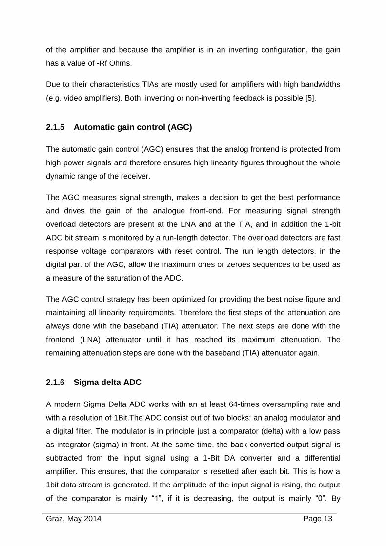
A modern Sigma Delta ADC works with an at least 64-times oversampling rate and
with a resolution of 1Bit.The ADC consist out of two blocks: an analog modulator and
a digital filter. The modulator is in principle just a comparator (delta) with a low pass
as integrator (sigma) in front. At the same time, the back-converted output signal is
subtracted from the input signal using a 1-Bit DA converter and a differential
amplifier. This ensures, that the comparator is resetted after each bit. This is how a
1bit data stream is generated. If the amplitude of the input signal is rising, the output
of the comparator is mainly “1”, if it is decreasing, the output is mainly “0”. By
Graz, May 2014 Page 14
integrating this bit stream (low pass), the analog signal could be regained
immediately [6]. Following figure shows the block diagram of such a sigma delta
ADC.
Figure 5: Block diagram of a first order SD ADC [1]
The implemented ADC is a 1-bit higher order oversampled SD-ADC. The output is a
single bit data-stream which is further processed by the digital baseband.
2.2 Digital IF preprocessing
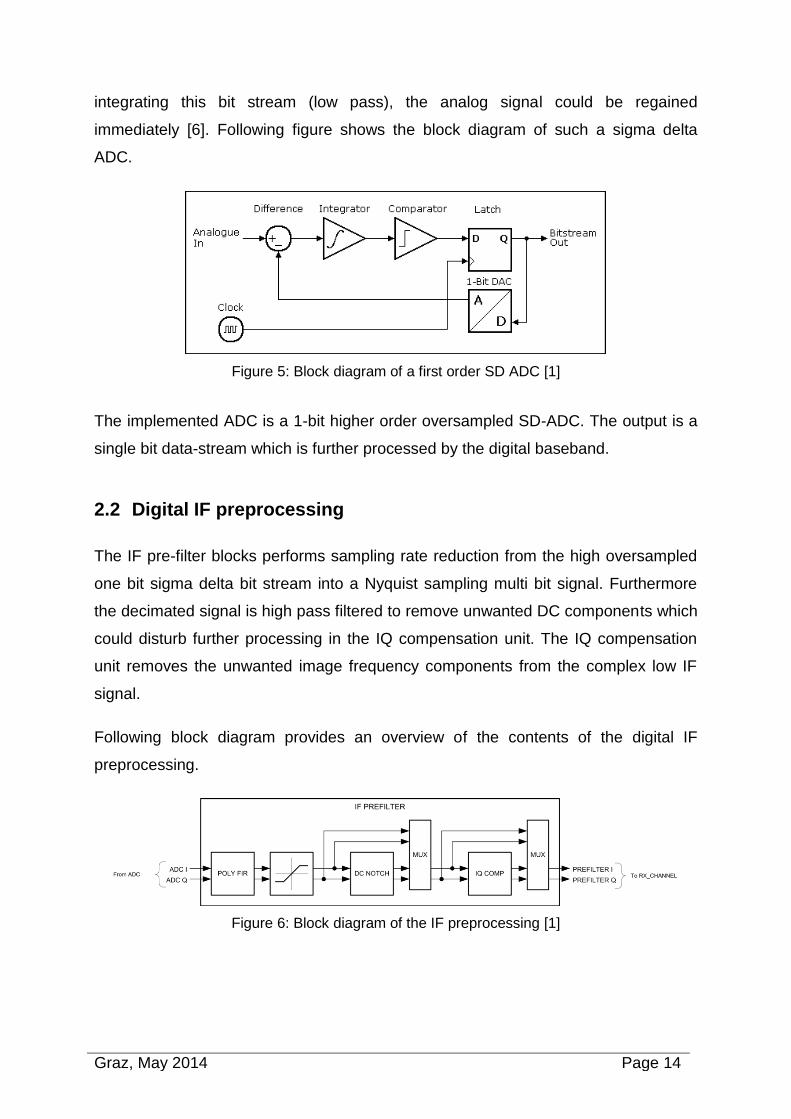
The IF pre-filter blocks performs sampling rate reduction from the high oversampled
one bit sigma delta bit stream into a Nyquist sampling multi bit signal. Furthermore
the decimated signal is high pass filtered to remove unwanted DC components which
could disturb further processing in the IQ compensation unit. The IQ compensation
unit removes the unwanted image frequency components from the complex low IF
signal.
Following block diagram provides an overview of the contents of the digital IF
preprocessing.
Figure 6: Block diagram of the IF preprocessing [1]
Graz, May 2014 Page 15
2.2.1 Decimation filter
The decimation filter restores the IF signal from the highly oversampled 1 bit data
stream of the sigma delta ADC at a sample rate of 3.6 MS/s. The decimation filter
has a fixed cut-off frequency of ~1 MHz with an almost flat pass band over the
supported intermediate frequency range from -900 kHz to 900 kHz.
By feeding the output of the sigma delta ADC into the decimation filter, it has to fulfill
three tasks: It has to filter out-of-band quantization noise, out-of-band signals present
in the modulator’s analog input and it has to lower the sampling frequency to a value
closer to two times the highest frequency of interest.
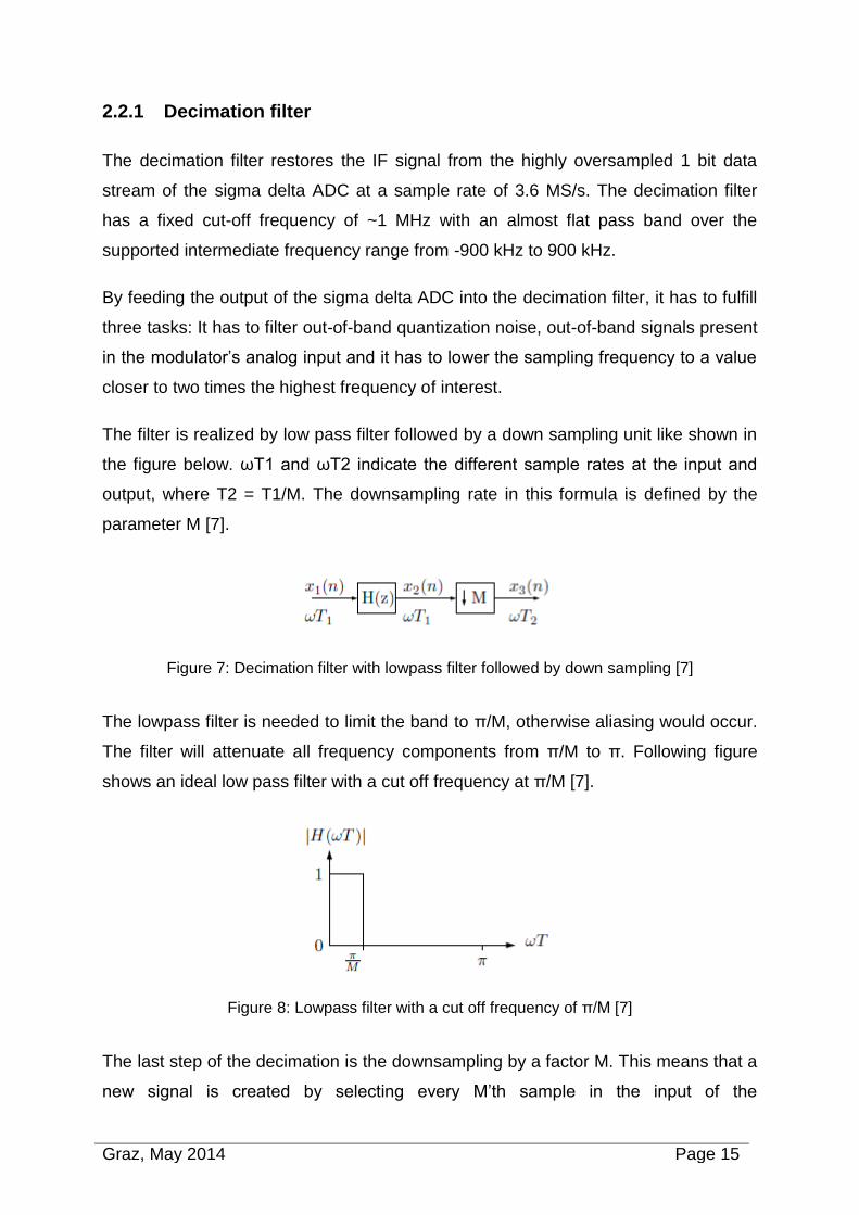
The filter is realized by low pass filter followed by a down sampling unit like shown in
the figure below. ωT1 and ωT2 indicate the different sample rates at the input and
output, where T2 = T1/M. The downsampling rate in this formula is defined by the
parameter M [7].
Figure 7: Decimation filter with lowpass filter followed by down sampling [7]
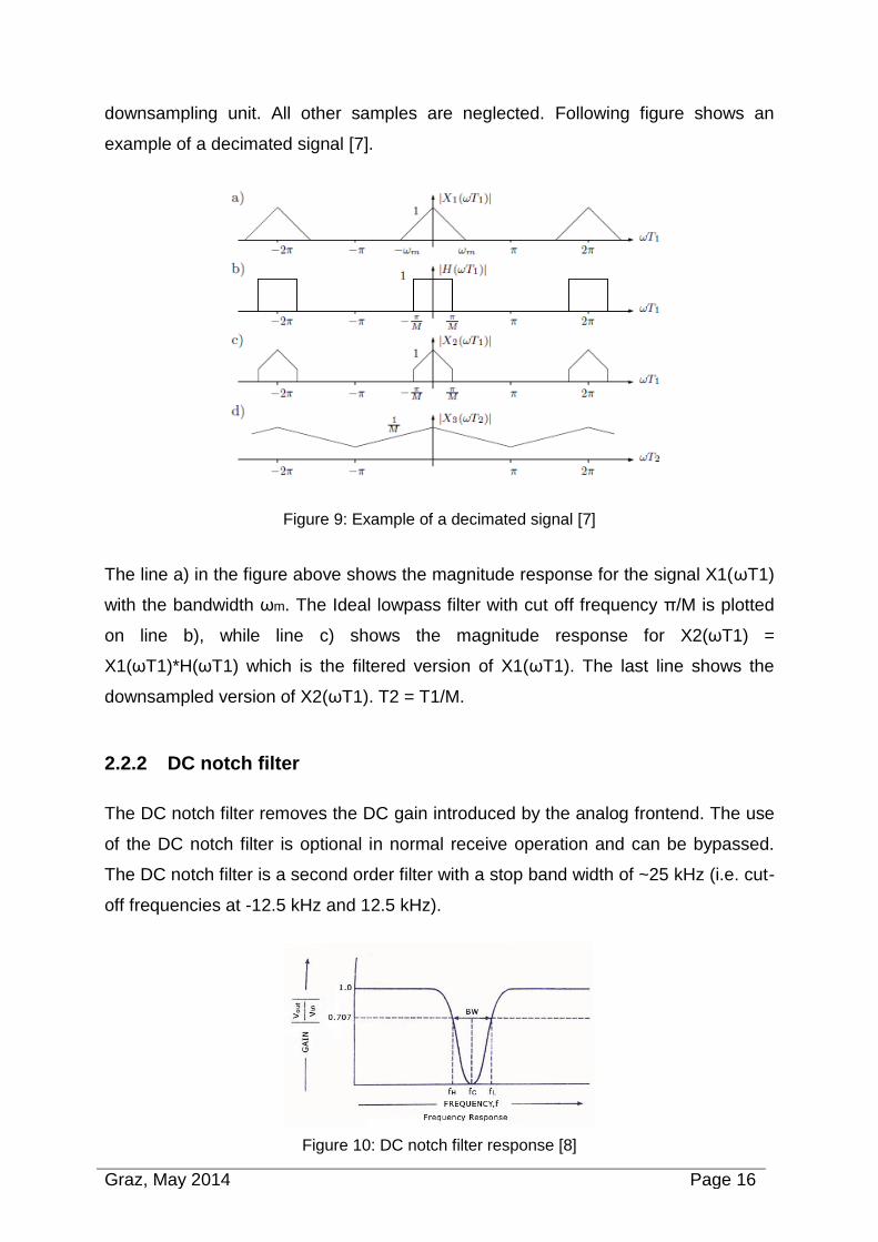
The lowpass filter is needed to limit the band to π/M, otherwise aliasing would occur.
The filter will attenuate all frequency components from π/M to π. Following figure
shows an ideal low pass filter with a cut off frequency at π/M [7].
Figure 8: Lowpass filter with a cut off frequency of π/M [7]
The last step of the decimation is the downsampling by a factor M. This means that a
new signal is created by selecting every M’th sample in the input of the
Graz, May 2014 Page 16
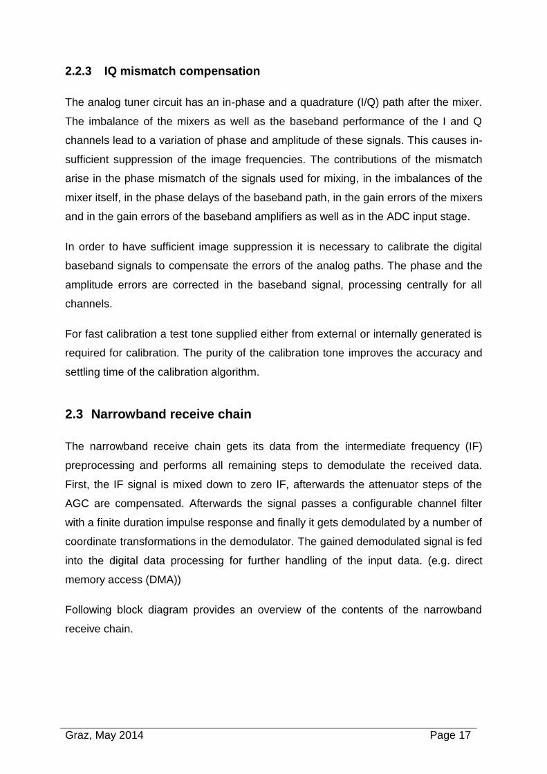
downsampling unit. All other samples are neglected. Following figure shows an
example of a decimated signal [7].
Figure 9: Example of a decimated signal [7]
The line a) in the figure above shows the magnitude response for the signal X1(ωT1)
with the bandwidth ωm. The Ideal lowpass filter with cut off frequency π/M is plotted
on line b), while line c) shows the magnitude response for X2(ωT1) =
X1(ωT1)*H(ωT1) which is the filtered version of X1(ωT1). The last line shows the
downsampled version of X2(ωT1). T2 = T1/M.
2.2.2 DC notch filter
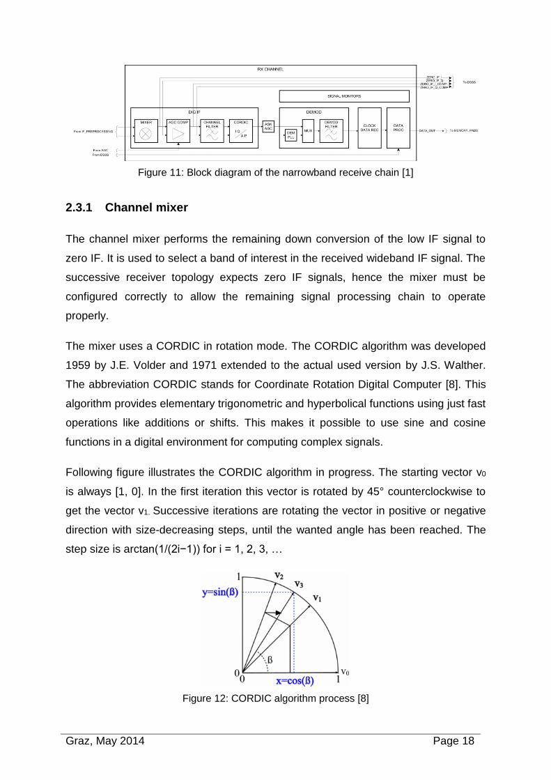
The DC notch filter removes the DC gain introduced by the analog frontend. The use
of the DC notch filter is optional in normal receive operation and can be bypassed.
The DC notch filter is a second order filter with a stop band width of ~25 kHz (i.e. cut-
off frequencies at -12.5 kHz and 12.5 kHz).
Figure 10: DC notch filter response [8]
Graz, May 2014 Page 17
2.2.3 IQ mismatch compensation
The analog tuner circuit has an in-phase and a quadrature (I/Q) path after the mixer.
The imbalance of the mixers as well as the baseband performance of the I and Q
channels lead to a variation of phase and amplitude of these signals. This causes in-
sufficient suppression of the image frequencies. The contributions of the mismatch
arise in the phase mismatch of the signals used for mixing, in the imbalances of the
mixer itself, in the phase delays of the baseband path, in the gain errors of the mixers
and in the gain errors of the baseband amplifiers as well as in the ADC input stage.
In order to have sufficient image suppression it is necessary to calibrate the digital
baseband signals to compensate the errors of the analog paths. The phase and the
amplitude errors are corrected in the baseband signal, processing centrally for all
channels.
For fast calibration a test tone supplied either from external or internally generated is
required for calibration. The purity of the calibration tone improves the accuracy and
settling time of the calibration algorithm.
2.3 Narrowband receive chain
The narrowband receive chain gets its data from the intermediate frequency (IF)
preprocessing and performs all remaining steps to demodulate the received data.
First, the IF signal is mixed down to zero IF, afterwards the attenuator steps of the
AGC are compensated. Afterwards the signal passes a configurable channel filter
with a finite duration impulse response and finally it gets demodulated by a number of
coordinate transformations in the demodulator. The gained demodulated signal is fed
into the digital data processing for further handling of the input data. (e.g. direct
memory access (DMA))
Following block diagram provides an overview of the contents of the narrowband
receive chain.
Graz, May 2014 Page 18
Figure 11: Block diagram of the narrowband receive chain [1]
2.3.1 Channel mixer
The channel mixer performs the remaining down conversion of the low IF signal to
zero IF. It is used to select a band of interest in the received wideband IF signal. The
successive receiver topology expects zero IF signals, hence the mixer must be
configured correctly to allow the remaining signal processing chain to operate
properly.
The mixer uses a CORDIC in rotation mode. The CORDIC algorithm was developed
1959 by J.E. Volder and 1971 extended to the actual used version by J.S. Walther.
The abbreviation CORDIC stands for Coordinate Rotation Digital Computer [8]. This
algorithm provides elementary trigonometric and hyperbolical functions using just fast
operations like additions or shifts. This makes it possible to use sine and cosine
functions in a digital environment for computing complex signals.
Following figure illustrates the CORDIC algorithm in progress. The starting vector v0
is always [1, 0]. In the first iteration this vector is rotated by 45° counterclockwise to
get the vector v1. Successive iterations are rotating the vector in positive or negative
direction with size-decreasing steps, until the wanted angle has been reached. The
step size is arctan(1/(2i−1)) for i = 1, 2, 3, …
Figure 12: CORDIC algorithm process [8]
Graz, May 2014 Page 19
Due to the CORDIC principle the IF signal is shifted by a phase increment to the
desired target frequency. Unlike other mixing principles this procedure does not
introduce any unwanted mixing products.
The programmable mixing frequency of the receiver ranges over the entire IF
bandwidth from -900 kHz to +900 kHz with a resolution of 100 Hz.
2.3.2 Channel filter
The channel filter allows the selection of a desired band of interest out of the
wideband IF signal. The filter cut-off frequency is selected by a configurable sample
rate conversion stage. For correct baseband operation, the maximum chip rate of the
wanted signal must not exceed a certain value.
The channel filter is realized with an FIR filter using a windowing function [9]. The
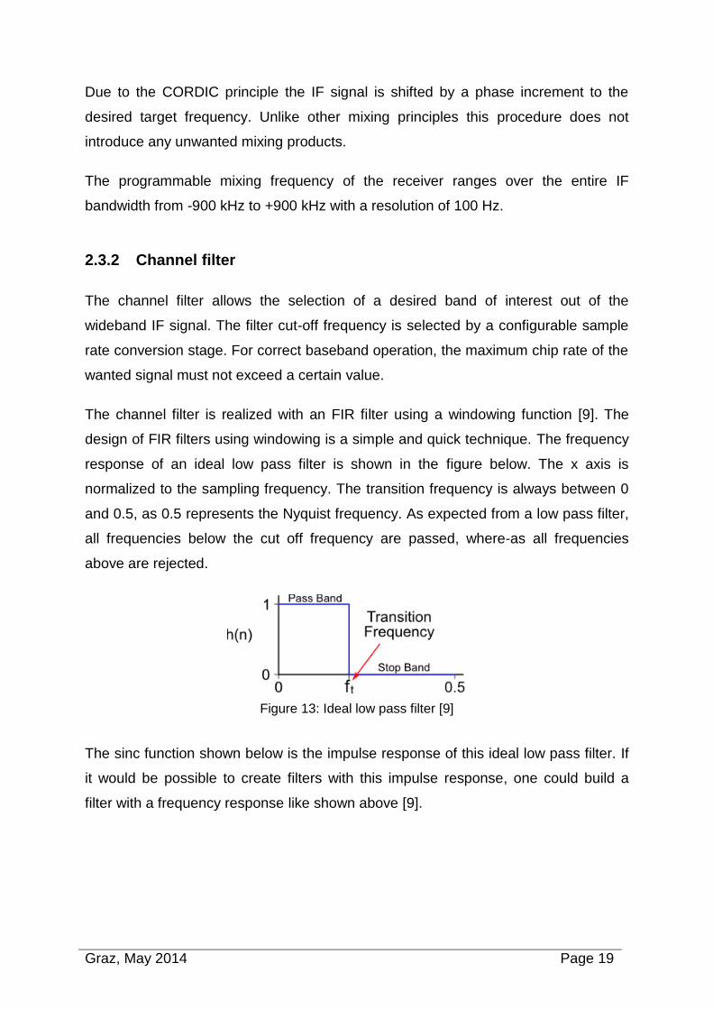
design of FIR filters using windowing is a simple and quick technique. The frequency
response of an ideal low pass filter is shown in the figure below. The x axis is
normalized to the sampling frequency. The transition frequency is always between 0
and 0.5, as 0.5 represents the Nyquist frequency. As expected from a low pass filter,
all frequencies below the cut off frequency are passed, where-as all frequencies
above are rejected.
Figure 13: Ideal low pass filter [9]
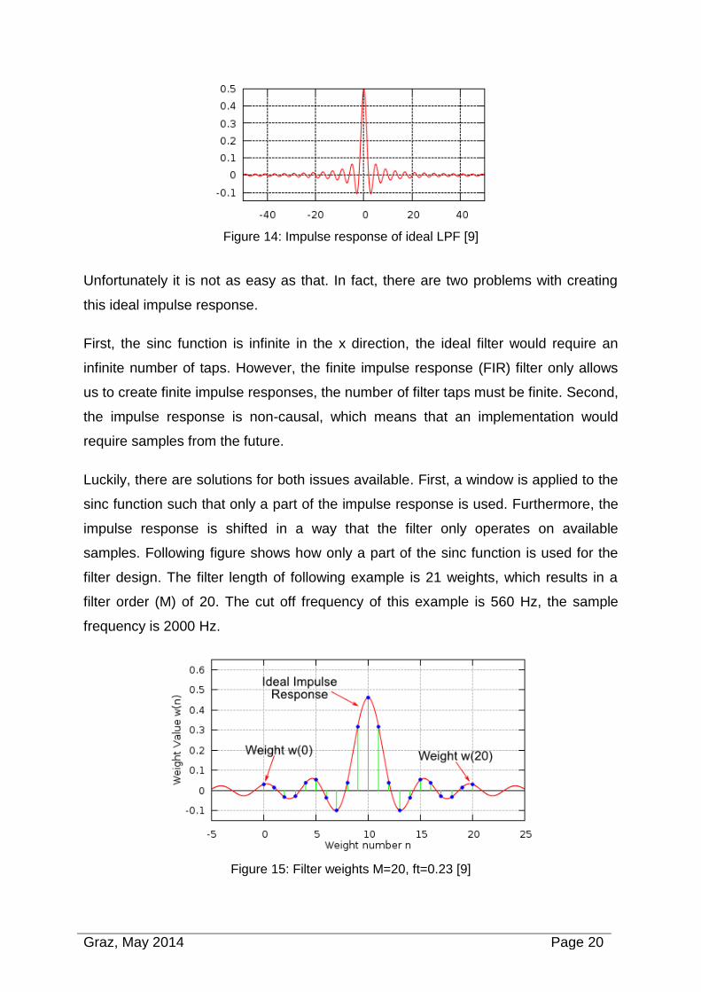
The sinc function shown below is the impulse response of this ideal low pass filter. If
it would be possible to create filters with this impulse response, one could build a
filter with a frequency response like shown above [9].
Graz, May 2014 Page 20
Figure 14: Impulse response of ideal LPF [9]
Unfortunately it is not as easy as that. In fact, there are two problems with creating
this ideal impulse response.
First, the sinc function is infinite in the x direction, the ideal filter would require an
infinite number of taps. However, the finite impulse response (FIR) filter only allows
us to create finite impulse responses, the number of filter taps must be finite. Second,
the impulse response is non-causal, which means that an implementation would
require samples from the future.
Luckily, there are solutions for both issues available. First, a window is applied to the
sinc function such that only a part of the impulse response is used. Furthermore, the
impulse response is shifted in a way that the filter only operates on available
samples. Following figure shows how only a part of the sinc function is used for the
filter design. The filter length of following example is 21 weights, which results in a
filter order (M) of 20. The cut off frequency of this example is 560 Hz, the sample
frequency is 2000 Hz.
Figure 15: Filter weights M=20, ft=0.23 [9]
Graz, May 2014 Page 21
By using following formulas, all the weights from 0 to 20 can be easily calculated.
With those the filter can be implemented.
Figure 16: Formulas to calculate the filter weights [9]
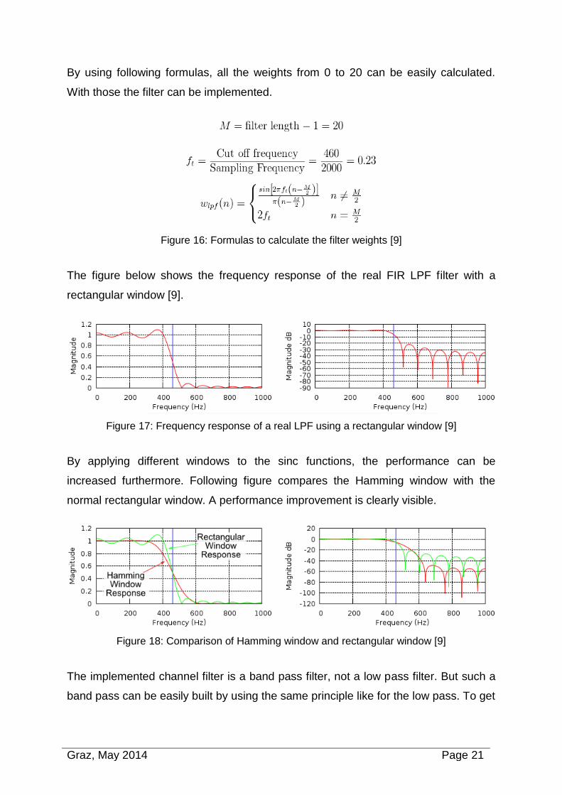
The figure below shows the frequency response of the real FIR LPF filter with a
rectangular window [9].
Figure 17: Frequency response of a real LPF using a rectangular window [9]
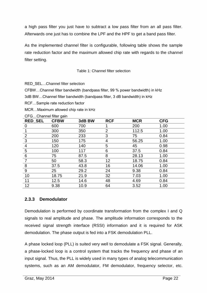
By applying different windows to the sinc functions, the performance can be
increased furthermore. Following figure compares the Hamming window with the
normal rectangular window. A performance improvement is clearly visible.
Figure 18: Comparison of Hamming window and rectangular window [9]
The implemented channel filter is a band pass filter, not a low pass filter. But such a
band pass can be easily built by using the same principle like for the low pass. To get
Graz, May 2014 Page 22
a high pass filter you just have to subtract a low pass filter from an all pass filter.
Afterwards one just has to combine the LPF and the HPF to get a band pass filter.
As the implemented channel filter is configurable, following table shows the sample
rate reduction factor and the maximum allowed chip rate with regards to the channel
filter setting.
Table 1: Channel filter selection
RED_SEL…Channel filter selection
CFBW…Channel filter bandwidth (bandpass filter, 99 % power bandwidth) in kHz
3dB BW…Channel filter bandwidth (bandpass filter, 3 dB bandwidth) in kHz
RCF…Sample rate reduction factor
MCR…Maximum allowed chip rate in kHz
CFG…Channel filter gain
RED_SEL CFBW 3dB BW RCF MCR CFG
0 600 700 1 200 1.00
1 300 350 2 112.5 1.00
2 200 233 3 75 0.84
3 150 175 4 56.25 1.00
4 120 140 5 45 0.98
5 100 117 6 37.5 0.84
6 75 87.5 8 28.13 1.00
7 50 58.3 12 18.75 0.84
8 37.5 43.8 16 14.06 1.00
9 25 29.2 24 9.38 0.84
10 18.75 21.9 32 7.03 1.00
11 12.5 14.6 48 4.69 0.84
12 9.38 10.9 64 3.52 1.00
2.3.3 Demodulator
Demodulation is performed by coordinate transformation from the complex I and Q
signals to real amplitude and phase. The amplitude information corresponds to the
received signal strength interface (RSSI) information and it is required for ASK
demodulation. The phase output is fed into a FSK demodulation PLL.
A phase locked loop (PLL) is suited very well to demodulate a FSK signal. Generally,
a phase-locked loop is a control system that tracks the frequency and phase of an
input signal. Thus, the PLL is widely used in many types of analog telecommunication
systems, such as an AM demodulator, FM demodulator, frequency selector, etc.
Graz, May 2014 Page 23
Similarly, a lot of digital phase-locked loops have been developed, e.g. to track a
carrier or synchronizing a bit signal in digital communication systems [10].
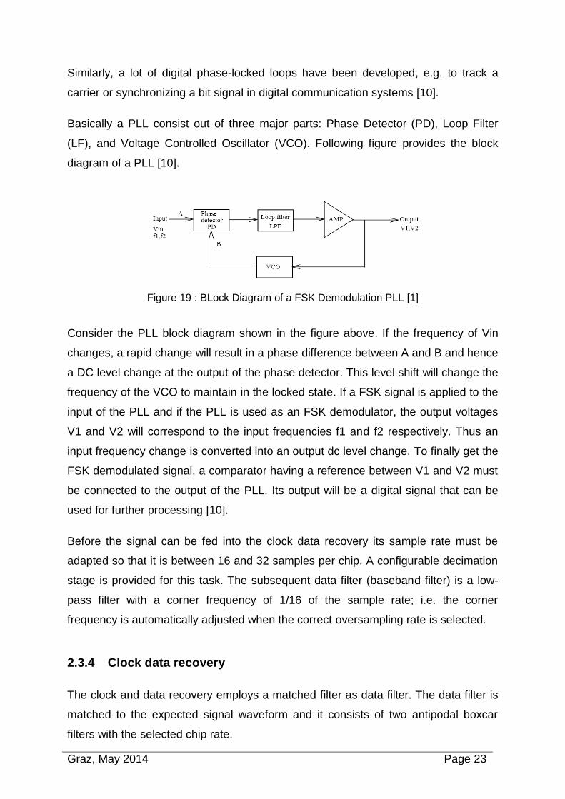
Basically a PLL consist out of three major parts: Phase Detector (PD), Loop Filter
(LF), and Voltage Controlled Oscillator (VCO). Following figure provides the block
diagram of a PLL [10].
Figure 19 : BLock Diagram of a FSK Demodulation PLL [1]
Consider the PLL block diagram shown in the figure above. If the frequency of Vin
changes, a rapid change will result in a phase difference between A and B and hence
a DC level change at the output of the phase detector. This level shift will change the
frequency of the VCO to maintain in the locked state. If a FSK signal is applied to the
input of the PLL and if the PLL is used as an FSK demodulator, the output voltages
V1 and V2 will correspond to the input frequencies f1 and f2 respectively. Thus an
input frequency change is converted into an output dc level change. To finally get the
FSK demodulated signal, a comparator having a reference between V1 and V2 must
be connected to the output of the PLL. Its output will be a digital signal that can be
used for further processing [10].
Before the signal can be fed into the clock data recovery its sample rate must be
adapted so that it is between 16 and 32 samples per chip. A configurable decimation
stage is provided for this task. The subsequent data filter (baseband filter) is a low-
pass filter with a corner frequency of 1/16 of the sample rate; i.e. the corner
frequency is automatically adjusted when the correct oversampling rate is selected.
2.3.4 Clock data recovery
The clock and data recovery employs a matched filter as data filter. The data filter is
matched to the expected signal waveform and it consists of two antipodal boxcar
filters with the selected chip rate.
Graz, May 2014 Page 24
A matched filter (originally known as a North filter [11]) is mainly used in signal
processing technologies. It is obtained by correlating a known signal, or template,
with an unknown signal to detect the presence of the template in the unknown signal.
This technique is equivalent to the convolution of the unknown signal with a
conjugated time-reversed version of the known signal. The matched filter is perfectly
suited for maximizing the signal to noise ratio (SNR) in the presence of additive
stochastic noise [12].
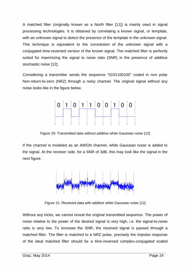
Considering a transmitter sends the sequence "0101100100" coded in non polar
Non-return-to-zero (NRZ) through a noisy channel. The original signal without any
noise looks like in the figure below.
Figure 20: Transmitted data without additive white Gaussian noise [12]
If the channel is modeled as an AWGN channel, white Gaussian noise is added to
the signal. At the receiver side, for a SNR of 3dB, this may look like the signal in the
next figure.
Figure 21: Received data with additive white Gaussian noise [12]
Without any tricks, we cannot reveal the original transmitted sequence. The power of
noise relative to the power of the desired signal is very high, i.e. the signal-to-noise
ratio is very low. To increase the SNR, the received signal is passed through a
matched filter. The filter is matched to a NRZ pulse, precisely the impulse response
of the ideal matched filter should be a time-reversed complex-conjugated scaled
Graz, May 2014 Page 25
version of the signal we are looking for. After convolving the noisy input signal with
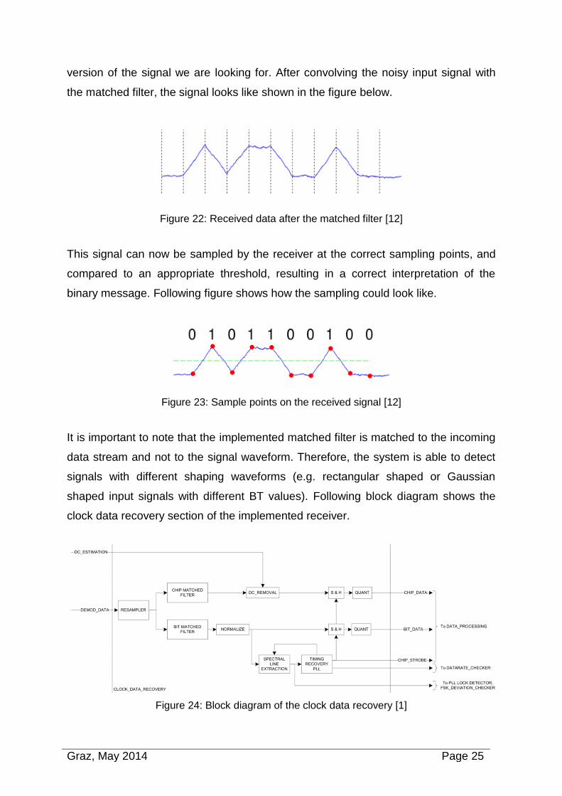
the matched filter, the signal looks like shown in the figure below.
Figure 22: Received data after the matched filter [12]
This signal can now be sampled by the receiver at the correct sampling points, and
compared to an appropriate threshold, resulting in a correct interpretation of the
binary message. Following figure shows how the sampling could look like.
Figure 23: Sample points on the received signal [12]
It is important to note that the implemented matched filter is matched to the incoming
data stream and not to the signal waveform. Therefore, the system is able to detect
signals with different shaping waveforms (e.g. rectangular shaped or Gaussian
shaped input signals with different BT values). Following block diagram shows the
clock data recovery section of the implemented receiver.
Figure 24: Block diagram of the clock data recovery [1]
Graz, May 2014 Page 26
The clock recovery consists of a fractional resampler stage which samples the
incoming data at a 16 x chip-oversampled nominal data rate. This ensures highest
sensitivity and best acquisition time also in presence of jammers and unwanted
signals. This input stream is filtered by a chip- and a bit-matched filter in order to
achieve data rate selective filtering. Using Manchester encoding, one bit is split into
two chips, therefore the bit matched filter always uses the information of two chips to
decode one bit of data. For the timing recovery, only the DC free bit matched filter
output is to be considered as it gives the best signal to noise performance. To ensure
the locking behavior of the timing recovery PLL, a static normalization stage levels
the output of the matched filter such that the PLL has input signals with constant
peak amplitudes. To improve the timing recovery, the chip rate is extracted from the
incoming data stream at the spectral line extraction unit together with time timing
recovery PLL.
The timing recovery PLL derives the chip clock out of the received data stream. The
chip clock is used to sample the bit matched filter output as well as the chip matched
filter output at the time instance where the signal power in the two filter outputs is
maximized.
The output of the chip matched filter is not DC free and contains in FSK the
frequency offset and in ASK a signal power dependent value. This DC component is
unwanted and is removed in the DC removal stage.
Finally the sampled values are quantized at the output stage to provide binary (0, 1)
data to the succeeding processing stages.
2.3.5 Data processing
The data processing block combines the functions of data recognition and packet
building for valid data sequences and accommodates the transfer to the memory of
the receiver. There are many functional blocks working together to carry out this
functionality. The core functionality is covered by the receiver finite state machine
(FSM).
Graz, May 2014 Page 27
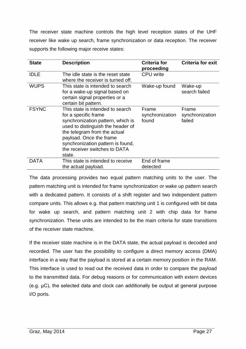
The receiver state machine controls the high level reception states of the UHF
receiver like wake up search, frame synchronization or data reception. The receiver
supports the following major receive states:
State Description Criteria for proceeding
Criteria for exit
IDLE The idle state is the reset state where the receiver is turned off.
CPU write
WUPS This state is intended to search for a wake-up signal based on certain signal properties or a certain bit pattern.
Wake-up found Wake-up search failed
FSYNC This state is intended to search for a specific frame synchronization pattern, which is used to distinguish the header of the telegram from the actual payload. Once the frame synchronization pattern is found, the receiver switches to DATA state.
Frame synchronization found
Frame synchronization failed
DATA This state is intended to receive the actual payload.
End of frame detected
The data processing provides two equal pattern matching units to the user. The
pattern matching unit is intended for frame synchronization or wake up pattern search
with a dedicated pattern. It consists of a shift register and two independent pattern
compare units. This allows e.g. that pattern matching unit 1 is configured with bit data
for wake up search, and pattern matching unit 2 with chip data for frame
synchronization. These units are intended to be the main criteria for state transitions
of the receiver state machine.
If the receiver state machine is in the DATA state, the actual payload is decoded and
recorded. The user has the possibility to configure a direct memory access (DMA)
interface in a way that the payload is stored at a certain memory position in the RAM.
This interface is used to read out the received data in order to compare the payload
to the transmitted data. For debug reasons or for communication with extern devices
(e.g. μC), the selected data and clock can additionally be output at general purpose
I/O ports.
Graz, May 2014 Page 28
2.4 Micro controller MRK3
This section provides an overview of the implemented microcontroller, type "MRK3".
It is the latest processor type from NXP. Furthermore this section explains how the
communication between the tool TestStation and the IC works.
2.4.1 Functional description
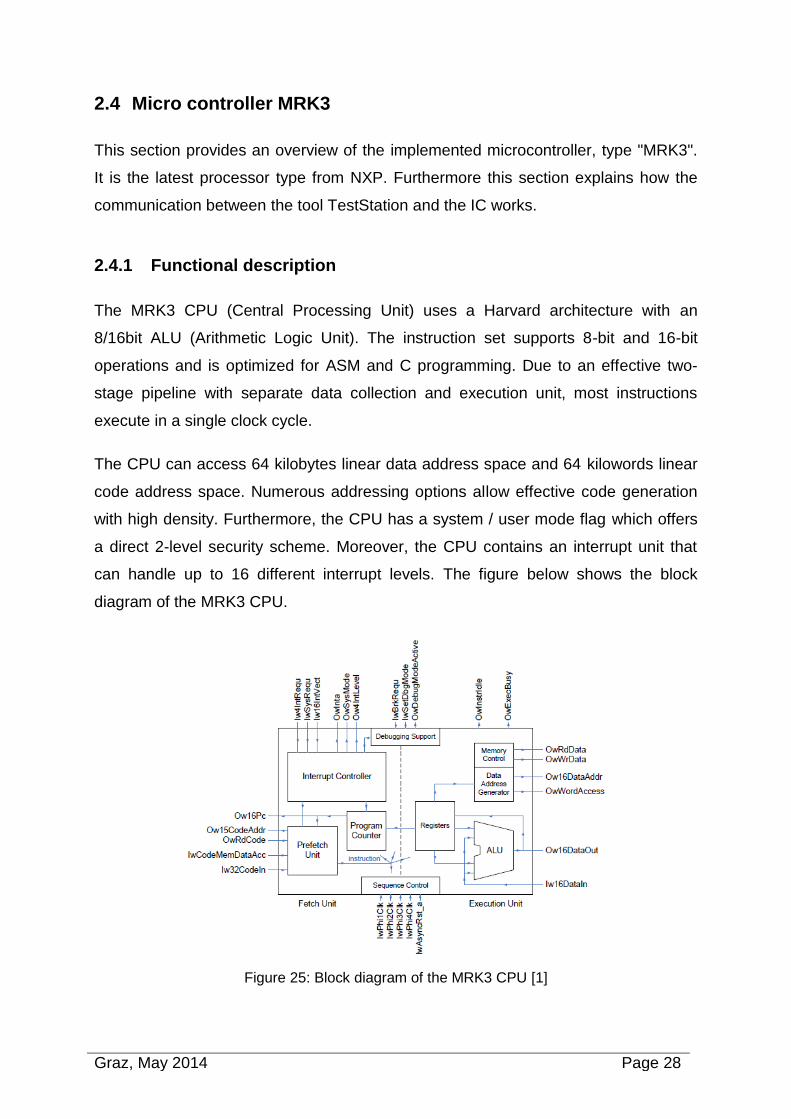
The MRK3 CPU (Central Processing Unit) uses a Harvard architecture with an
8/16bit ALU (Arithmetic Logic Unit). The instruction set supports 8-bit and 16-bit
operations and is optimized for ASM and C programming. Due to an effective two-
stage pipeline with separate data collection and execution unit, most instructions
execute in a single clock cycle.
The CPU can access 64 kilobytes linear data address space and 64 kilowords linear
code address space. Numerous addressing options allow effective code generation
with high density. Furthermore, the CPU has a system / user mode flag which offers
a direct 2-level security scheme. Moreover, the CPU contains an interrupt unit that
can handle up to 16 different interrupt levels. The figure below shows the block
diagram of the MRK3 CPU.
Figure 25: Block diagram of the MRK3 CPU [1]
Graz, May 2014 Page 29
Roughly speaking, the MRK3 architecture consists of two pipeline units. The fetch
unit and the execution unit. The task of the fetch unit is to ensure the correct program
flow, which is why it also contains the program counter and the interrupt controller.
Furthermore if fetches the collection of code words from the code memory and
provides a sequence of executable instructions to the execution unit.
The execution unit performs the data manipulation in the CPU. It calculates data
addresses for memory instructions read operands from registers and / or from the
memory, executes the requested command, writes the result of the operation back
into a register or in the memory and updates, if necessary, the status flags.
2.4.2 Monitor and download interface
The communication between the micro controller of NXPs modern ICs and the
TestStation is done via a communication protocol called monitor and download
interface (MDI). This protocol is NXP self-made and implemented in the ROM code of
the ICs. The interface is a two-wire serial synchronous interface consisting of two
pins: MSDA (data) and MSCL (clock)
The MSCL pin provides the bit clock and is always driven by the chip. As long as the
chip is in the reset state, the MSCL remains low. When the chip gets active, it sets
MSCL to high.
The MSDA pin is a bi-directional pin and receives / writes the data bits, depending on
the direction of data. The default state is HIGH, thus the IC connects an internal pull
up resistor to the pin, when it is in reset state.
Available debug functions of the monitor and download interface:
• Starting the user application in real time or single step mode
• Interrupt the user application
• Interrupt the user application using breakpoints
• Read / write CPU register contents
• Read / write RAM contents
• Read / write application code from / to the non-volatile memories
• Non-intrusive read the device status
• Protection of the application code and application data
Graz, May 2014 Page 30
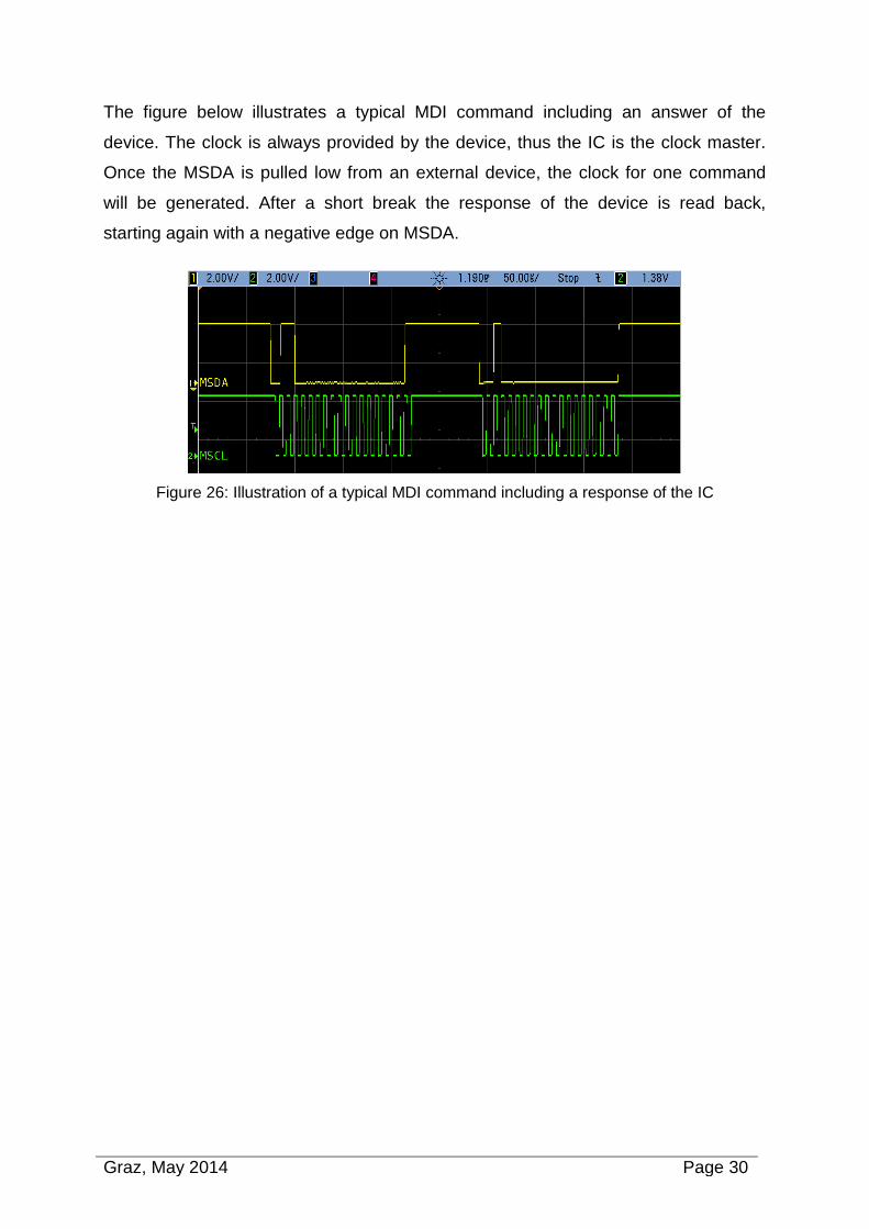
The figure below illustrates a typical MDI command including an answer of the
device. The clock is always provided by the device, thus the IC is the clock master.
Once the MSDA is pulled low from an external device, the clock for one command
will be generated. After a short break the response of the device is read back,
starting again with a negative edge on MSDA.
Figure 26: Illustration of a typical MDI command including a response of the IC
Graz, May 2014 Page 31
3. Measurement procedures and standards
This chapter describes the measurement procedures to be carried out on the
automated test bench in detail. Also the engineer standards defining the
measurements as well as the limits will be documented. Following table lists all the
use cases that should be tested. All the measurement procedures listed below shall
be carried out on each of these use cases.
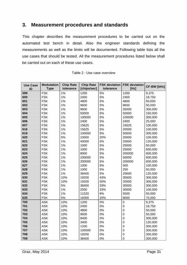
Table 2 : Use case overview
Use Case ID
Modulation Type
Chip Rate tolerance
Chip Rate [chips/sec]
FSK deviation tolerance
FSK deviation [Hz]
CF-BW [kHz]
599 FSK 1% 1200 5% 1200 9,375
600 FSK 1% 2400 5% 2400 18,750
601 FSK 1% 4800 5% 4800 50,000
602 FSK 1% 9600 5% 9600 50,000
603 FSK 1% 9600 5% 35000 300,000
604 FSK 1% 50000 5% 50000 150,000
605 FSK 1% 100000 5% 100000 300,000
606 FSK 1% 2400 5% 2400 25,000
607 FSK 1% 15625 5% 15625 100,000
616 FSK 1% 15625 5% 20000 100,000
619 FSK 1% 100000 5% 50000 300,000
620 FSK 5% 10000 20% 20000 100,000
621 FSK 1% 40000 5% 20000 120,000
622 FSK 1% 1000 5% 25000 50,000
623 FSK 1% 1000 5% 25000 600,000
624 FSK 1% 8000 5% 200000 600,000
625 FSK 1% 200000 5% 50000 600,000
626 FSK 1% 200000 5% 200000 600,000
627 FSK 1% 1000 5% 500 100,000
628 FSK 1% 1000 5% 250 50,000
629 FSK 1% 38400 5% 20000 120,000
630 FSK 10% 19200 43% 35000 300,000
631 FSK 10% 19200 50% 20000 300,000
632 FSK 5% 38400 33% 30000 300,000
633 FSK 1% 2000 33% 30000 100,000
634 FSK 1% 11520 9% 5500 50,000
635 FSK 5% 16000 20% 8000 75,000
700 ASK 10% 1200 0% 0 9,375
701 ASK 10% 2400 0% 0 18,750
702 ASK 10% 4800 0% 0 50,000
703 ASK 10% 9600 0% 0 50,000
704 ASK 10% 8400 0% 0 300,000
705 ASK 10% 3400 0% 0 120,000
706 ASK 10% 1200 0% 0 300,000
707 ASK 10% 100000 0% 0 300,000
708 ASK 10% 19200 0% 0 300,000
709 ASK 10% 38400 0% 0 300,000
Graz, May 2014 Page 32
3.1 Receiver sensitivity
The receiver sensitivity is the minimum level of signal (electromotive force (emf)) at
the receiver input, produced by a carrier at the nominal frequency of the receiver,
modulated with the normal test signal modulation, which produces one of the general
performance criteria stated below [14].
For the purpose of the receiver performance tests, the receiver shall produce an
appropriate output after modulation under normal conditions as indicated below.
a data signal with a bit error ratio of 10-2 without correction or
a message acceptance ratio of 80 %
3.1.1 Method of measurement with continuous bit streams
In digital transmission, a bit error is a received bit extracted from a data stream,
received over a communication channel that has been corrupted due to noise,
interference, distortion or bit synchronization errors.
The bit error rate (BER) is the number of bit errors divided by the total number of
transmitted bits during a certain time interval. BER is a unit less performance
measure, often expressed as a percentage.
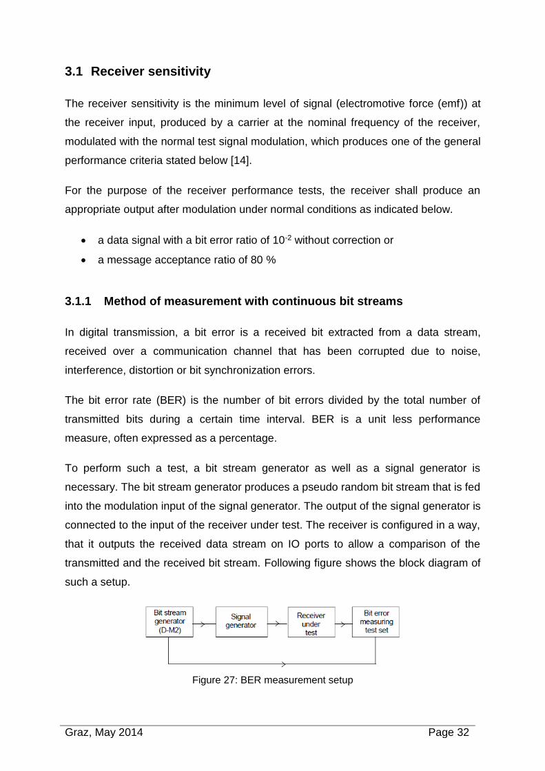
To perform such a test, a bit stream generator as well as a signal generator is
necessary. The bit stream generator produces a pseudo random bit stream that is fed
into the modulation input of the signal generator. The output of the signal generator is
connected to the input of the receiver under test. The receiver is configured in a way,
that it outputs the received data stream on IO ports to allow a comparison of the
transmitted and the received bit stream. Following figure shows the block diagram of
such a setup.
Figure 27: BER measurement setup
Graz, May 2014 Page 33
The bit stream of the modulated signal shall be compared to the bit stream obtained
from the receiver output after demodulation. The level of the input signal to the
receiver shall be reduced until the bit error rate is 10-3 or better. This input level is the
sensitivity level, it shall be stored for post processing.
3.1.2 Method of measurement with messages
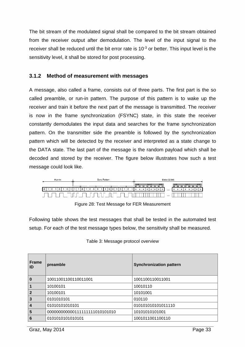
A message, also called a frame, consists out of three parts. The first part is the so
called preamble, or run-in pattern. The purpose of this pattern is to wake up the
receiver and train it before the next part of the message is transmitted. The receiver
is now in the frame synchronization (FSYNC) state, in this state the receiver
constantly demodulates the input data and searches for the frame synchronization
pattern. On the transmitter side the preamble is followed by the synchronization
pattern which will be detected by the receiver and interpreted as a state change to
the DATA state. The last part of the message is the random payload which shall be
decoded and stored by the receiver. The figure below illustrates how such a test
message could look like.
Figure 28: Test Message for FER Measurement
Following table shows the test messages that shall be tested in the automated test
setup. For each of the test message types below, the sensitivity shall be measured.
Table 3: Message protocol overview
Frame ID
preamble Synchronization pattern
0 10011001100110011001 1001100110011001
1 10100101 10010110
2 10100101 10101001
3 0101010101 010110
4 01010101010101 010101010101011110
5 000000000000111111111010101010 10101010101001
6 0101010101010101 1001011001100110
Graz, May 2014 Page 34
7 0101010110 01011001100110
8 0110011001100110 10100110010110101001011001100110
9 011001100110 01100000000001100110
10 110011001100110011001100 111000111000111000
11 101010101010 1111100110101
12 101010101010 11100010010
13 101010101010 10101010100101101001100110
14 101010101010 1010100101011001011001
15 01010101010101010101010101010101010101010101010101010101010101010
101010101001011001011010
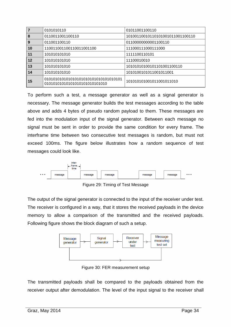
To perform such a test, a message generator as well as a signal generator is
necessary. The message generator builds the test messages according to the table
above and adds 4 bytes of pseudo random payload to them. These messages are
fed into the modulation input of the signal generator. Between each message no
signal must be sent in order to provide the same condition for every frame. The
interframe time between two consecutive test messages is random, but must not
exceed 100ms. The figure below illustrates how a random sequence of test
messages could look like.
Figure 29: Timing of Test Message
The output of the signal generator is connected to the input of the receiver under test.
The receiver is configured in a way, that it stores the received payloads in the device
memory to allow a comparison of the transmitted and the received payloads.
Following figure shows the block diagram of such a setup.
Figure 30: FER measurement setup
The transmitted payloads shall be compared to the payloads obtained from the
receiver output after demodulation. The level of the input signal to the receiver shall
Graz, May 2014 Page 35
be reduced until the frame error rate is 10-2 or better. This input level is the sensitivity
level, it shall be stored for post processing.
3.2 Receiver jammer performance
Beside the sensitivity of the receiver, the jammer performance is a very important
parameter of the system. It must be guaranteed, that the receiver still operates with
its full functionality, if an interferer is added on the wanted signal. Therefore three
different interferer types are tested to ensure a proper functionality in the application.
The jammer types are:
CW: non modulated carrier
AM: Amplitude modulation with 80% modulation depth and 200 Hz data rate
FM: Frequency modulation with 20 kHz frequency deviation and 1250 Hz data
rate
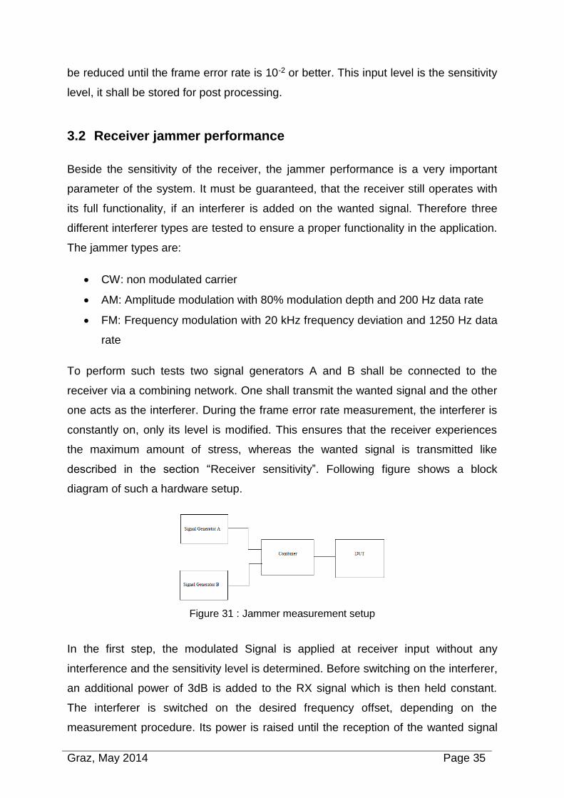
To perform such tests two signal generators A and B shall be connected to the
receiver via a combining network. One shall transmit the wanted signal and the other
one acts as the interferer. During the frame error rate measurement, the interferer is
constantly on, only its level is modified. This ensures that the receiver experiences
the maximum amount of stress, whereas the wanted signal is transmitted like
described in the section “Receiver sensitivity”. Following figure shows a block
diagram of such a hardware setup.
Figure 31 : Jammer measurement setup
In the first step, the modulated Signal is applied at receiver input without any
interference and the sensitivity level is determined. Before switching on the interferer,
an additional power of 3dB is added to the RX signal which is then held constant.
The interferer is switched on the desired frequency offset, depending on the
measurement procedure. Its power is raised until the reception of the wanted signal
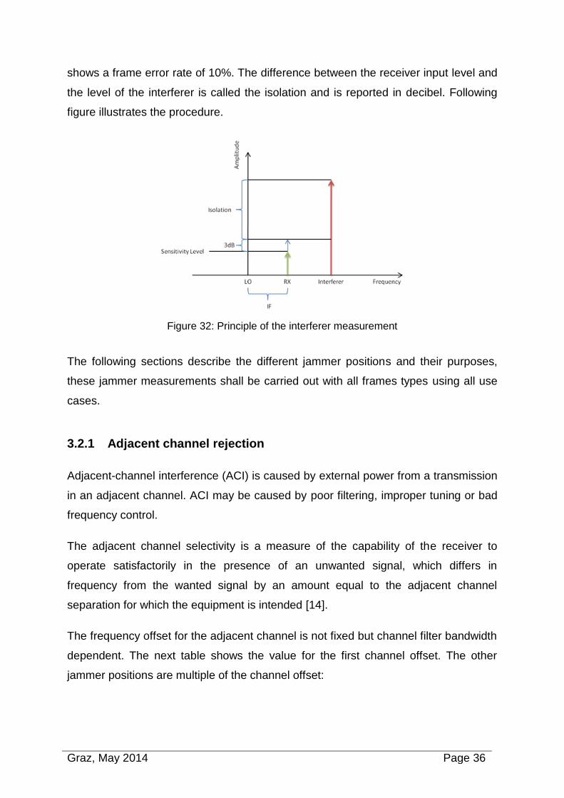
Graz, May 2014 Page 36
shows a frame error rate of 10%. The difference between the receiver input level and
the level of the interferer is called the isolation and is reported in decibel. Following
figure illustrates the procedure.
Figure 32: Principle of the interferer measurement
The following sections describe the different jammer positions and their purposes,
these jammer measurements shall be carried out with all frames types using all use
cases.
3.2.1 Adjacent channel rejection
Adjacent-channel interference (ACI) is caused by external power from a transmission
in an adjacent channel. ACI may be caused by poor filtering, improper tuning or bad
frequency control.
The adjacent channel selectivity is a measure of the capability of the receiver to
operate satisfactorily in the presence of an unwanted signal, which differs in
frequency from the wanted signal by an amount equal to the adjacent channel
separation for which the equipment is intended [14].
The frequency offset for the adjacent channel is not fixed but channel filter bandwidth
dependent. The next table shows the value for the first channel offset. The other
jammer positions are multiple of the channel offset:
Graz, May 2014 Page 37
Table 4 : Channel separation for each channel filter bandwidth
Channel filter bandwidth Adjacent channel separation
10 kHz 12.5 kHz
50 kHz 100 kHz
300 kHz 500 kHz
All other Channel filter bandwidth + 25%
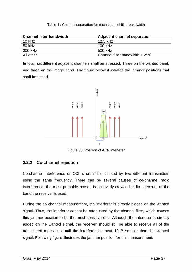
In total, six different adjacent channels shall be stressed. Three on the wanted band,
and three on the image band. The figure below illustrates the jammer positions that
shall be tested.
Figure 33: Position of ACR interferer
3.2.2 Co-channel rejection
Co-channel interference or CCI is crosstalk, caused by two different transmitters
using the same frequency. There can be several causes of co-channel radio
interference, the most probable reason is an overly-crowded radio spectrum of the
band the receiver is used.
During the co channel measurement, the interferer is directly placed on the wanted
signal. Thus, the interferer cannot be attenuated by the channel filter, which causes
this jammer position to be the most sensitive one. Although the interferer is directly
added on the wanted signal, the receiver should still be able to receive all of the
transmitted messages until the interferer is about 10dB smaller than the wanted
signal. Following figure illustrates the jammer position for this measurement.
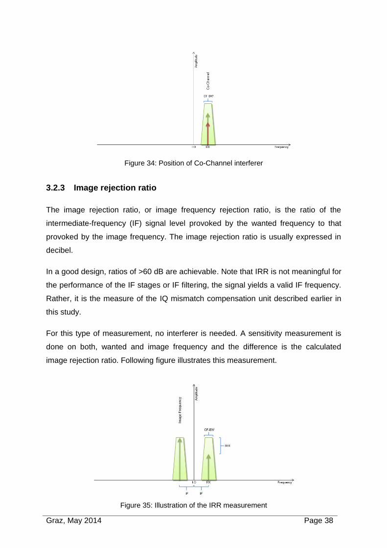
Graz, May 2014 Page 38
Figure 34: Position of Co-Channel interferer
3.2.3 Image rejection ratio
The image rejection ratio, or image frequency rejection ratio, is the ratio of the
intermediate-frequency (IF) signal level provoked by the wanted frequency to that
provoked by the image frequency. The image rejection ratio is usually expressed in
decibel.
In a good design, ratios of >60 dB are achievable. Note that IRR is not meaningful for
the performance of the IF stages or IF filtering, the signal yields a valid IF frequency.
Rather, it is the measure of the IQ mismatch compensation unit described earlier in
this study.
For this type of measurement, no interferer is needed. A sensitivity measurement is
done on both, wanted and image frequency and the difference is the calculated
image rejection ratio. Following figure illustrates this measurement.
Figure 35: Illustration of the IRR measurement
Graz, May 2014 Page 39
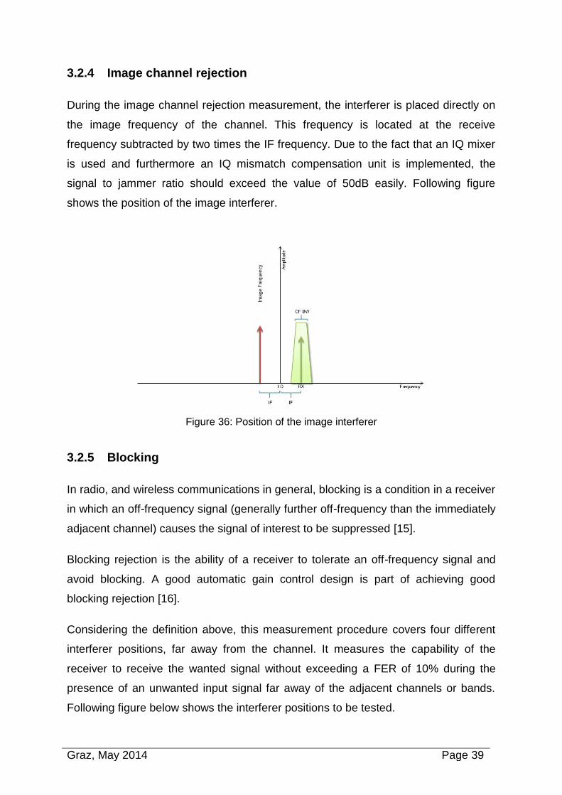
3.2.4 Image channel rejection
During the image channel rejection measurement, the interferer is placed directly on
the image frequency of the channel. This frequency is located at the receive
frequency subtracted by two times the IF frequency. Due to the fact that an IQ mixer
is used and furthermore an IQ mismatch compensation unit is implemented, the
signal to jammer ratio should exceed the value of 50dB easily. Following figure
shows the position of the image interferer.
Figure 36: Position of the image interferer
3.2.5 Blocking
In radio, and wireless communications in general, blocking is a condition in a receiver
in which an off-frequency signal (generally further off-frequency than the immediately
adjacent channel) causes the signal of interest to be suppressed [15].
Blocking rejection is the ability of a receiver to tolerate an off-frequency signal and
avoid blocking. A good automatic gain control design is part of achieving good
blocking rejection [16].
Considering the definition above, this measurement procedure covers four different
interferer positions, far away from the channel. It measures the capability of the
receiver to receive the wanted signal without exceeding a FER of 10% during the
presence of an unwanted input signal far away of the adjacent channels or bands.
Following figure below shows the interferer positions to be tested.
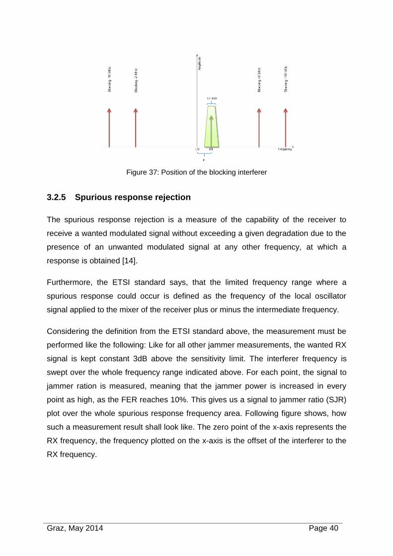
Graz, May 2014 Page 40
Figure 37: Position of the blocking interferer
3.2.5 Spurious response rejection
The spurious response rejection is a measure of the capability of the receiver to
receive a wanted modulated signal without exceeding a given degradation due to the
presence of an unwanted modulated signal at any other frequency, at which a
response is obtained [14].
Furthermore, the ETSI standard says, that the limited frequency range where a
spurious response could occur is defined as the frequency of the local oscillator
signal applied to the mixer of the receiver plus or minus the intermediate frequency.
Considering the definition from the ETSI standard above, the measurement must be
performed like the following: Like for all other jammer measurements, the wanted RX
signal is kept constant 3dB above the sensitivity limit. The interferer frequency is
swept over the whole frequency range indicated above. For each point, the signal to
jammer ration is measured, meaning that the jammer power is increased in every
point as high, as the FER reaches 10%. This gives us a signal to jammer ratio (SJR)
plot over the whole spurious response frequency area. Following figure shows, how
such a measurement result shall look like. The zero point of the x-axis represents the
RX frequency, the frequency plotted on the x-axis is the offset of the interferer to the
RX frequency.
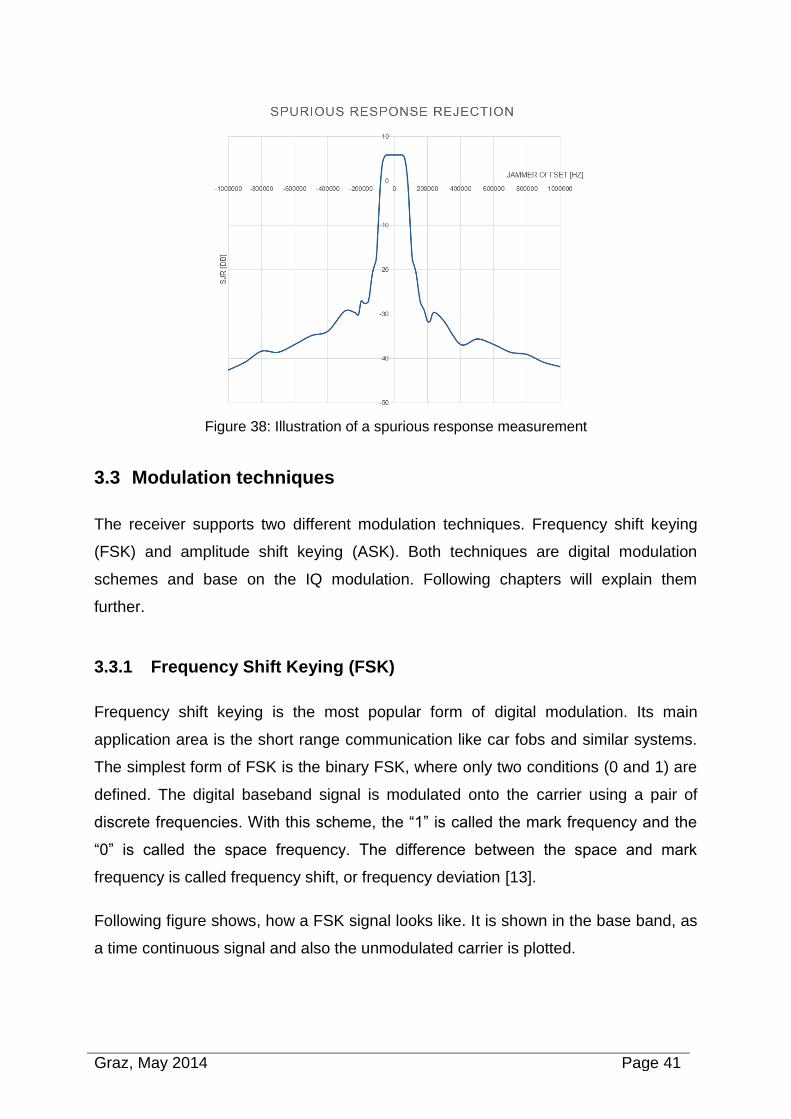
Graz, May 2014 Page 41
Figure 38: Illustration of a spurious response measurement
3.3 Modulation techniques
The receiver supports two different modulation techniques. Frequency shift keying
(FSK) and amplitude shift keying (ASK). Both techniques are digital modulation
schemes and base on the IQ modulation. Following chapters will explain them
further.
3.3.1 Frequency Shift Keying (FSK)
Frequency shift keying is the most popular form of digital modulation. Its main
application area is the short range communication like car fobs and similar systems.
The simplest form of FSK is the binary FSK, where only two conditions (0 and 1) are
defined. The digital baseband signal is modulated onto the carrier using a pair of
discrete frequencies. With this scheme, the “1” is called the mark frequency and the
“0” is called the space frequency. The difference between the space and mark
frequency is called frequency shift, or frequency deviation [13].
Following figure shows, how a FSK signal looks like. It is shown in the base band, as
a time continuous signal and also the unmodulated carrier is plotted.
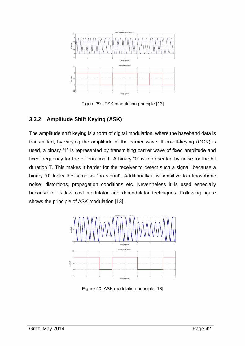
Graz, May 2014 Page 42
Figure 39 : FSK modulation principle [13]
3.3.2 Amplitude Shift Keying (ASK)
The amplitude shift keying is a form of digital modulation, where the baseband data is
transmitted, by varying the amplitude of the carrier wave. If on-off-keying (OOK) is
used, a binary “1” is represented by transmitting carrier wave of fixed amplitude and
fixed frequency for the bit duration T. A binary “0” is represented by noise for the bit
duration T. This makes it harder for the receiver to detect such a signal, because a
binary “0” looks the same as “no signal”. Additionally it is sensitive to atmospheric
noise, distortions, propagation conditions etc. Nevertheless it is used especially
because of its low cost modulator and demodulator techniques. Following figure
shows the principle of ASK modulation [13].
Figure 40: ASK modulation principle [13]
Graz, May 2014 Page 43
4. Implementation
In this chapter the final implementation will be presented. The first section will discuss
the pros and cons of the verification using an FPGA and explains how such a FPGA
can be used to fulfill the task of this study.
In the second section the hardware setup will be explained. Starting from a block
diagram, every part of the setup, like the signal generator or the tool used for
communication and modulation will be documented and discussed.
The implemented software is discussed in the third section. Not only one software
was needed to get the system working, there are programs running on the micro
controller of the front end IC, on the micro controller synthesized in the FPGA, on the
communication and modulation box called “TestStation”, as well as on the host
computer.
4.1 FPGA - Field Programmable Gate Array
This section will answer all question regarding the keyword FPGA. It will explain what
an FPGA is, how it can be used for this application and what limitations one has to
cope with. Furthermore the strength and weaknesses of a verification using a FPGA
will be discussed. One will experience, that such a verification has a lot more pros
than cons, which is also the reason why this study gained a lot of interest within NXP
Semiconductors.
A field-programmable gate array (FPGA) is an integrated circuit that can be
configured by the end customer or a designer after manufacturing, that’s why the
name includes "field-programmable". The FPGA configuration is done via a hardware
description language (HDL), like for all digital designs in an integrated circuit.
Modern FPGAs provide large numbers of logic gates and RAM blocks to enable the
implementation of complex digital computations. FPGAs can be used to implement
any logical function that an application-specific integrated circuit (ASIC) could
perform. The ability to program the functionality after manufacturing, perform rapid
prototyping of the design and the low engineering costs relative to an ASIC design,
offer advantages for many applications.
Graz, May 2014 Page 44
4.1.1 Functional description
FPGAs contain configurable logic blocks, called CLBs or LABs, depending on the
vendor. These CLBs are connected using configurable interconnects that allow the
blocks to be wired together. This means, that many logic gates can be wired in many
different configurations. Logic blocks can be configured to perform complex
combinational functions, or as simple logic gates like AND or NOT. Most FPGAs also
include memory elements like simple flip-flops or complete blocks of memory like
RAMs [17].
Furthermore, input / output blocks (IO-blocks) are implemented on most of the
modern FPGAs. They are used to communicate with the surrounding environment
and are built to pass through the incoming signals to the configurable logic blocks.
Also these blocks are configurable and can be suited to the application environment.
For example, the output voltage as well as the input thresholds can be adapted to
different standards like TTL or CMOS. Also driving strength and input impedance can
be controlled.
To map an application circuit into a field programmable gate array, a FPGA with
adequate resources must be chosen. While the number of CLBs and I/Os required
for a design is easily determined, the number of routing tracks needed may vary
considerably even among designs with the same amount of logic.
4.1.2 Hardware structure
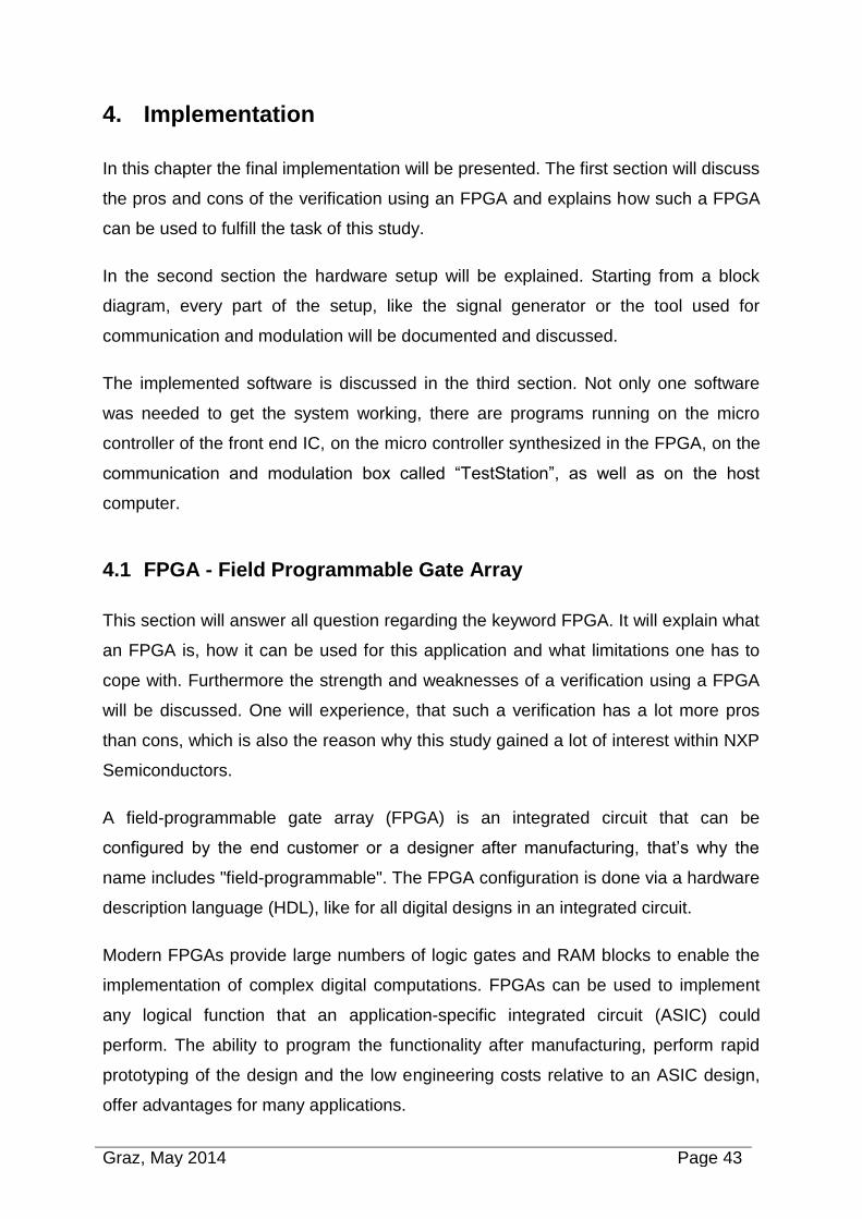
A logic block (CLB) consists only of a few logical cells. A typical cell consists of a 4-
input look up table (LUT), a full adder (FA) and a D-type flip-flop, as shown in the
figure below. The LUTs in this figure are split into two 3-input LUTs, in the normal
mode those are combined to a 4-input LUT. In arithmetic mode, their outputs are fed
to the full adder. The mode selection is defined via the middle multiplexer. The output
can be either synchronous or asynchronous, depending on the programming of the
multiplexer to the right [17].
Graz, May 2014 Page 45
Figure 41: Block diagram of a configurable logic block [17]
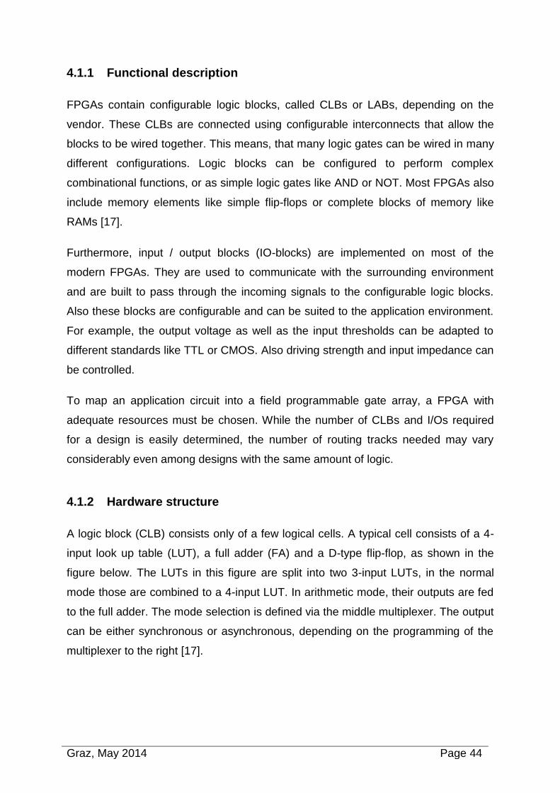
Whenever a horizontal and a vertical channel intersect, there is a so called switch
box integrated. One possible implementation of such a switchbox is, that a wire
entering a switch box can be connected to one out of three other wires in adjacent
channel segments. The figure below illustrates the connections in a switch box [18].
Figure 42: Connections in a switch box [18]
4.1.3 Design and synthesis
To configure the behavior of the FPGA, the user must use a hardware description
language (HDL) to define the logic behavior of his design. The HDL is most of the
times VHDL or Verilog, but also other languages are allowed. Once the code is
finished, it can be used on any FPGA or even be used for an ASIC design.
Every vendor provides a tool, to convert the hardware description language into a so-
called netlist, which is a list containing all the connection information of the used
digital cells from the design. This procedure is called synthesis. This netlist isn’t a
well readable code anymore, but modern tools allow to look at the produced cells and
their connection visually. The netlist can then be fitted to the actual FPGA
architecture using a process called place-and-route, usually performed by the FPGA
vendor's place-and-route software. For place and route a detailed description of the
used hardware is necessary. This hardware description contains the number and
Graz, May 2014 Page 46
structure of the CLBs, the number and type of interconnects as well as the number of
IO blocks. Once the process is complete, the binary file generated by the tool is used
to configure the FPGA. This file is transferred to the FPGA via a serial interface
(JTAG) or to an external memory device like an EEPROM [19].
4.1.4 Motivation for FPGA verification
The main verification solution is of course the digital simulation. Designing a test
bench for a new digital block of the IC can require more working time than the design
of the digital block itself. Nevertheless such a test bench is needed for every sub-
block of the digital backend to prove its correct functionality. Therefore the digital
design team introduced default use cases and a so called reference frame, which is
an example of a modulated input signal fed into the digital receiver. All the
simulations are done with this reference frame for all use cases. The simulation
coverage is quite low if just one input frame and some chip rate / modulation index
combinations are used. Unfortunately the simulation time is very high for such test
benches, therefore the simulation coverage can’t be increased easily. This limitation
is also limiting the quality of the design itself, because a solid verification is the key to
success in such design projects. Carrying out parts of the verification with a FPGA
environment could increase the verification coverage enormously. More protocols
and use cases could be tested and potential errors could be found faster.
One essential drawback of the digital simulation are the models of the transmitters
and interferers as well as the models of the analog receiver frontend. All of the
models are developed in computing tools like Matlab or similar and although they are
fitting the real behavior very well, there is still a remaining uncertainty in terms of
dynamic behavior etc. Therefore it is hard to determine if a simulation result is
hundred percent representative for the final ASIC including the analog functionality.
Choosing a FPGA verification is the best way to overcome this uncertainty, because
real transmitters and the final analog front end are used to produce the input for the
digital receiver chain.
Nowadays the time to market of an IC must be as short as possible, as the customer
demand for new technology is constantly high. In a normal design process the
customer has to wait with the implementation of his software and his use cases until
Graz, May 2014 Page 47
the first tested prototypes of the IC are available. This includes also the fab run which
takes more than 6 weeks. If anything is delayed during the bring-up phase of the
supplier (in this particular case NXP), this also shortens the remaining
implementation time of the customer before the product is released. Providing a
FPGA solution to the customer helps to overcome this delay. He can use the FPGA
for the debugging of his software as well as for implementing his receiver use cases.
When the first prototypes of the IC arrive at the customer, the same software without
any modifications can be used. Also the configuration for the receiver are 100%
compatible with the FPGA system.
4.1.5 Strengths
As the FPGA is re-configurable, potentially found errors can be fixed in the design
and after a new run of synthesis and place and route the verification can continue.
This way of working is called rapid prototyping, because errors can be found, fixed
and verified very fast. If errors are found in the prototype on silicon base, a new fab
run requires more than six weeks until the fixed version is available.
Once the FPGA system is up and running, more than one setup can run in parallel to
produce even more output for the verification of the design. The number of
simulations in parallel is limited by the amount of server computation capacity
booked. Such computation capacity is very expensive, thus two or more FPGA
setups in parallel are the cheapest solution to verify the design with a high test
coverage.
As the test time of the FPGA system is very short compared to the simulation time,
lots of use cases and protocols can be tested in a short time frame. Also the number
of tested frames to distinguish the frame error rate can be quite high. In simulation
this number has to be limited as it is crucial for the simulation time.
All of the firmware developed for the FPGA system can be reused without any
modifications on the final IC. This is possible because the micro controller and its
surrounding blocks like the memories are also synthesized in the FPGA. Therefore
the software team can already debug their code before the prototype is available.
This ensures a very short debugging time on the real IC.
Graz, May 2014 Page 48
One essential point to mention is, that the FPGA system already emulates the final
IC. Therefore the test bench and its configurations can be fully reused for the
verification of the silicon. The only thing that has to be updated, are the potential
changes in the configuration of the analog front end compared to the one which was
used for the FPGA verification. But except this small part, everything is plug and play
when the prototype arrives. Therefore no double work is needed and the bring-up
phase of the IC can be very short.
4.1.6 Weaknesses and limitations
To implement a digital design for the FPGA environment, some extra work of the
digital design team is necessary. The whole implementation time could easily have a
duration of more than one week, which is a lot in critical project phases. But it is
worth to mention, that this implementation only has to be done once.
Of course cost is an important factor for the feasibility of the FPGA verification setup.
Especially the signal generators needed for the bench are quite expensive. The
FPGA board also costs in the range of a few thousand euros. Therefore not any
number of setups can be built without exceeding the cost limit of the project.
None of the control signals that are routed from the analog part of the receiver are
available in the FPGA application. The most important information that has to be
passed to the digital part of the receiver are the ADC output signals (I and Q) as well
as the ADC clock signal. Those can be multiplexed to a MFIO of the front end IC and
thus passed to the MFIOs of the FPGA. The only control signal that cannot be
forwarded, is the input for the AGC compensation unit. This units would scale the
incoming data dependent from the attenuator settings at the frontend. In the FPGA
implementation this compensation must be turned off.
Due to the fact that only one receive chain fits into the FPGA, parallel reception
cannot be tested. In the final IC three receive chains are able to operate in parallel
and decode signals from three different transmitters at the same time (considering
the dynamic input range of the receiver).
One drawback of the FPGA verification is of course, that the exact timing behavior of
the final IC cannot be modeled. Only the pure functionality can be tested. Thus, race
Graz, May 2014 Page 49
conditions, spikes as well as correct sample and hold times cannot be verified. This is
also the reason why simulation will never be neglected in a professional verification
strategy.
Additionally, the behavior over temperature and supply voltage also cannot be
verified as the temperature behavior and the dependency on the supply voltage is
mostly process dependent. The only thing that could be done, is to stress the analog
frontend which produces the data for the digital receive chain. But as the FPGA test
bench is built to test the digital functionality and not the analog one, such tests are
not planned.
The prerequisite of such a FPGA based verification is of course, that the analog front
end of the receiver to be verified is either already available on a test chip, or does not
change tremendously compared to the previous version of the receiver. This is the
case because a verification of the digital part of the receiver makes no sense, if the
analog part (e.g. the Sigma Delta ADC) changes dramatically. Aim of the FPGA
based verification is to test the whole system, frontend as well as backend.
4.1.7 Implementation effort
As the design was initially written to be embedded in an ASIC, there is some effort
needed to make it synthesizable for a standalone FPGA application. The block which
should be tested, the narrowband receive chain, will not work without its surrounding
environment like the clock tree, the micro controller or the memories.
Therefore the digital design team developed a design which is suited for the usage
on any FPGA, containing the most important functionalities of the ASIC including the
micro controller, all memories, the main clock source as well as most of the IOs. Most
important is of course the implementation of the digital receiver, but because of
space limitations mentioned above, only one of the three receive chains is included.
Thus, a wrapper has been built around the top-level digital part of the IC, called
cai_mtci_fpga_top. It implements clock and reset generation, the port logic and the
page flash. The next figure shows the block diagram of this implementation.
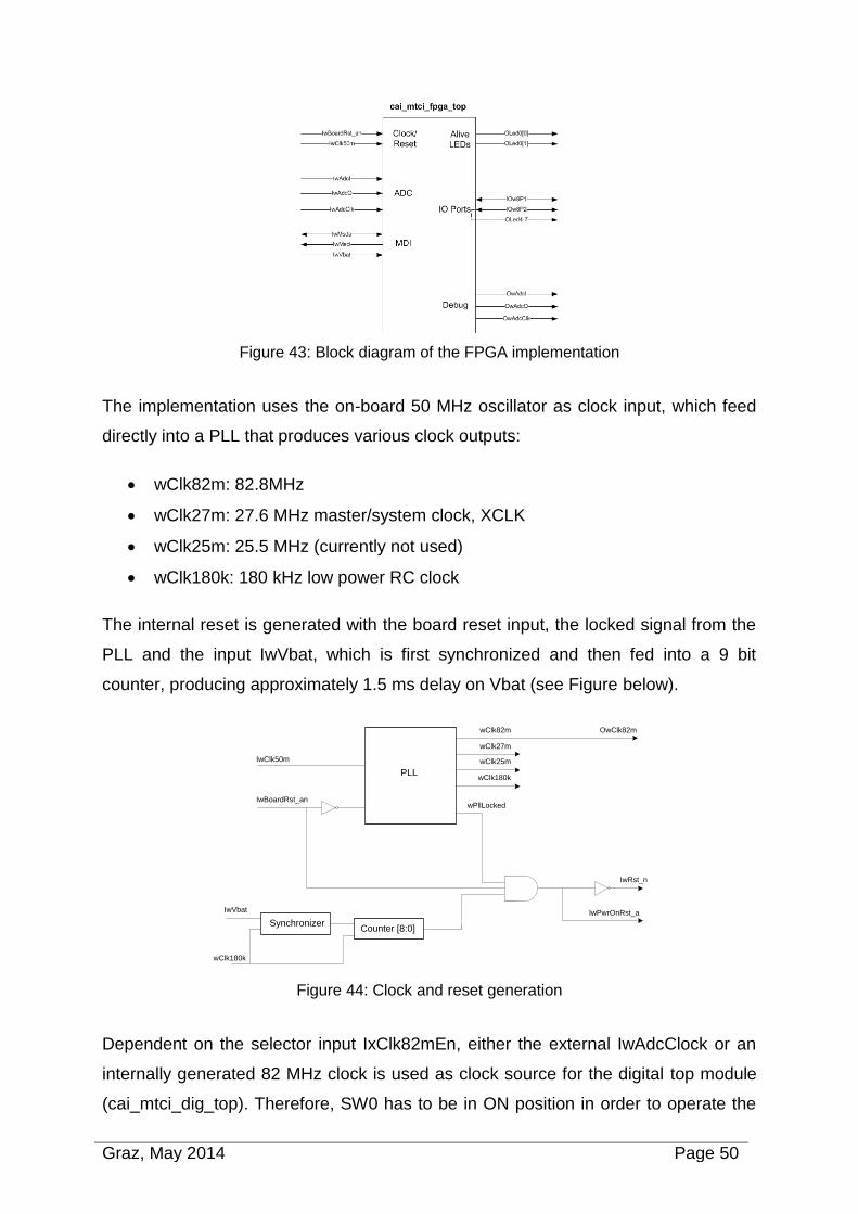
Graz, May 2014 Page 50
Figure 43: Block diagram of the FPGA implementation
The implementation uses the on-board 50 MHz oscillator as clock input, which feed
directly into a PLL that produces various clock outputs:
wClk82m: 82.8MHz
wClk27m: 27.6 MHz master/system clock, XCLK
wClk25m: 25.5 MHz (currently not used)
wClk180k: 180 kHz low power RC clock
The internal reset is generated with the board reset input, the locked signal from the
PLL and the input IwVbat, which is first synchronized and then fed into a 9 bit
counter, producing approximately 1.5 ms delay on Vbat (see Figure below).
IwBoardRst_an
wClk82m
PLL
wClk27m
wClk25m
wClk180k
wPllLocked
IwClk50m
SynchronizerCounter [8:0]
IwVbat
wClk180k
IwPwrOnRst_a
IwRst_n
OwClk82m
Figure 44: Clock and reset generation
Dependent on the selector input IxClk82mEn, either the external IwAdcClock or an
internally generated 82 MHz clock is used as clock source for the digital top module
(cai_mtci_dig_top). Therefore, SW0 has to be in ON position in order to operate the
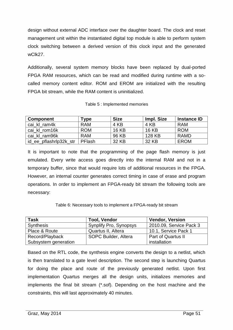
Graz, May 2014 Page 51
design without external ADC interface over the daughter board. The clock and reset
management unit within the instantiated digital top module is able to perform system
clock switching between a derived version of this clock input and the generated
wClk27.
Additionally, several system memory blocks have been replaced by dual-ported
FPGA RAM resources, which can be read and modified during runtime with a so-
called memory content editor. ROM and EROM are initialized with the resulting
FPGA bit stream, while the RAM content is uninitialized.
Table 5 : Implemented memories
Component Type Size Impl. Size Instance ID
cai_kl_ram4k RAM 4 KB 4 KB RAM
cai_kl_rom16k ROM 16 KB 16 KB ROM
cai_kl_ram96k RAM 96 KB 128 KB RAMD
id_ee_pflashrlp32k_str PFlash 32 KB 32 KB EROM
It is important to note that the programming of the page flash memory is just
emulated. Every write access goes directly into the internal RAM and not in a
temporary buffer, since that would require lots of additional resources in the FPGA.
However, an internal counter generates correct timing in case of erase and program
operations. In order to implement an FPGA-ready bit stream the following tools are
necessary:
Table 6: Necessary tools to implement a FPGA-ready bit stream
Task Tool, Vendor Vendor, Version
Synthesis Synplify Pro, Synopsys 2010.09, Service Pack 3
Place & Route Quartus II, Altera 10.1, Service Pack 1
Record/Playback Subsystem generation
SOPC Builder, Altera Part of Quartus II installation
Based on the RTL code, the synthesis engine converts the design to a netlist, which
is then translated to a gate level description. The second step is launching Quartus
for doing the place and route of the previously generated netlist. Upon first
implementation Quartus merges all the design units, initializes memories and
implements the final bit stream (*.sof). Depending on the host machine and the
constraints, this will last approximately 40 minutes.
Graz, May 2014 Page 52
4.2 Hardware setup
This section will describe the implemented hardware setup and all of its components
in detail. The block diagram below illustrates which components are in use and how
they are connected.
Figure 45: Block diagram of the hardware setup
The host of the setup is a personal computer (PC), it remote controls the signal
generator as well as the tool TestStation which will be described below. Furthermore
the PC is also used to download the configuration in the FPGA.
A very important part of the setup is the NXP self-made tool called TestStation. It is
used to communicate with the RF frontend IC as well as with the IC synthesized in
the FPGA. Furthermore it also forms the messages that are sent to the receiver. This
is done by passing the base band data from the TestStation to the external
modulation input of the signal generator.
The output of the signal generator is connected to evaluation board of the NXP
frontend IC. The IC on this board is a predecessor of the product that shall be
verified, whereas the analog part of the IC nearly remains unchanged. It is configured
in a way that the ADC stream is outputted to IO ports, where the signal can be
tapped and passed to the input of the FPGA.
Graz, May 2014 Page 53
The peak to peak voltage of the ADC stream outputted by the frontend IC is only in
the range of 300mV. With such a small amplitude it is hard to be sampled by the
input IOs of the FPGA, therefore a level shifter board is placed between the analog
frontend and the FPGA evaluation board. It converts the 300mV peak-peak voltage
to digital signal with an amplitude of about 3.3V using comparator circuits.
The FPGA is used in combination with an evaluation board provided by the company
Altera. This board provides lots of connectors, buttons, LEDs, etc. to enable all of the
features of the FPGA. Furthermore also an on-board 50 MHz oscillator is available
which is used for internal clock generation. Beside a complete power management
system with lots of available power supply outputs, this boards also contains a USB
to JTAG interface, which enables easy programming via a personal computer.
4.2.1 Analog frontend
In order to use an already existing receiver type from NXP as an analog frontend, the
RF evaluation board of the used IC is used. The evaluation board is seen in the
figure below. The board provides the connectivity to all RF pins of the device as well
as to the MFIO ports.
For the purpose of the FPGA test bench the receiver input is of course very
important, thus the matching network that matches the receiver input to 50Ohm is
necessary. On the used IC as well as on the evaluation board two different receiver
input pins are available. Therefore two different matching networks for two different
frequency bands can be used.
The communication interface MDI which is described in a different section of this
study, is routed to a 5-Pin connector of the evaluation board. These pins must be
connected to the communication tool TestStation.
The ADC interface pins, where the 300mV Vpp ADC Stream is outputted shall be
connected to the input of the level shifter board. This can be done either with
shielded cables or by stacking the evaluation board onto the level shifter board. To
go for the second opportunity, one has to solder the connector on the bottom side of
the board instead of original position on the front side.
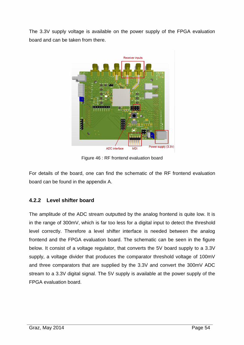
Graz, May 2014 Page 54
The 3.3V supply voltage is available on the power supply of the FPGA evaluation
board and can be taken from there.
Figure 46 : RF frontend evaluation board
For details of the board, one can find the schematic of the RF frontend evaluation
board can be found in the appendix A.
4.2.2 Level shifter board
The amplitude of the ADC stream outputted by the analog frontend is quite low. It is
in the range of 300mV, which is far too less for a digital input to detect the threshold
level correctly. Therefore a level shifter interface is needed between the analog
frontend and the FPGA evaluation board. The schematic can be seen in the figure
below. It consist of a voltage regulator, that converts the 5V board supply to a 3.3V
supply, a voltage divider that produces the comparator threshold voltage of 100mV
and three comparators that are supplied by the 3.3V and convert the 300mV ADC
stream to a 3.3V digital signal. The 5V supply is available at the power supply of the
FPGA evaluation board.
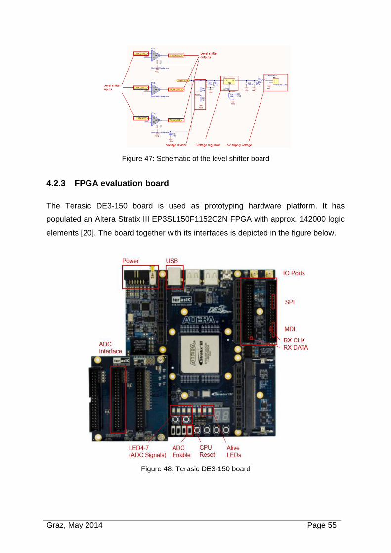
Graz, May 2014 Page 55
Figure 47: Schematic of the level shifter board
4.2.3 FPGA evaluation board
The Terasic DE3-150 board is used as prototyping hardware platform. It has
populated an Altera Stratix III EP3SL150F1152C2N FPGA with approx. 142000 logic
elements [20]. The board together with its interfaces is depicted in the figure below.
Figure 48: Terasic DE3-150 board
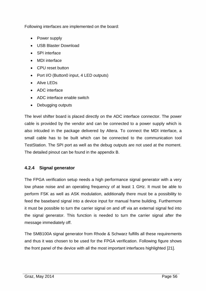
Graz, May 2014 Page 56
Following interfaces are implemented on the board:
Power supply
USB Blaster Download
SPI interface
MDI interface
CPU reset button
Port I/O (Button0 input, 4 LED outputs)
Alive LEDs
ADC interface
ADC interface enable switch
Debugging outputs
The level shifter board is placed directly on the ADC interface connector. The power
cable is provided by the vendor and can be connected to a power supply which is
also inlcuded in the package delivered by Altera. To connect the MDI interface, a
small cable has to be built which can be connected to the communication tool
TestStation. The SPI port as well as the debug outputs are not used at the moment.
The detailed pinout can be found in the appendix B.
4.2.4 Signal generator
The FPGA verification setup needs a high performance signal generator with a very
low phase noise and an operating frequency of at least 1 GHz. It must be able to
perform FSK as well as ASK modulation, additionally there must be a possibility to
feed the baseband signal into a device input for manual frame building. Furthermore
it must be possible to turn the carrier signal on and off via an external signal fed into
the signal generator. This function is needed to turn the carrier signal after the
message immediately off.
The SMB100A signal generator from Rhode & Schwarz fulfills all these requirements
and thus it was chosen to be used for the FPGA verification. Following figure shows
the front panel of the device with all the most important interfaces highlighted [21].
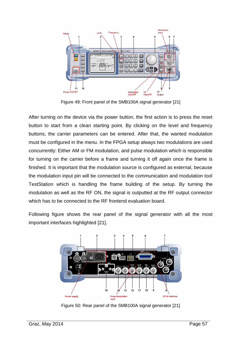
Graz, May 2014 Page 57
Figure 49: Front panel of the SMB100A signal generator [21]
After turning on the device via the power button, the first action is to press the reset
button to start from a clean starting point. By clicking on the level and frequency
buttons, the carrier parameters can be entered. After that, the wanted modulation
must be configured in the menu. In the FPGA setup always two modulations are used
concurrently: Either AM or FM modulation, and pulse modulation which is responsible
for turning on the carrier before a frame and turning it off again once the frame is
finished. It is important that the modulation source is configured as external, because
the modulation input pin will be connected to the communication and modulation tool
TestStation which is handling the frame building of the setup. By turning the
modulation as well as the RF ON, the signal is outputted at the RF output connector
which has to be connected to the RF frontend evaluation board.
Following figure shows the rear panel of the signal generator with all the most
important interfaces highlighted [21].
Figure 50: Rear panel of the SMB100A signal generator [21]
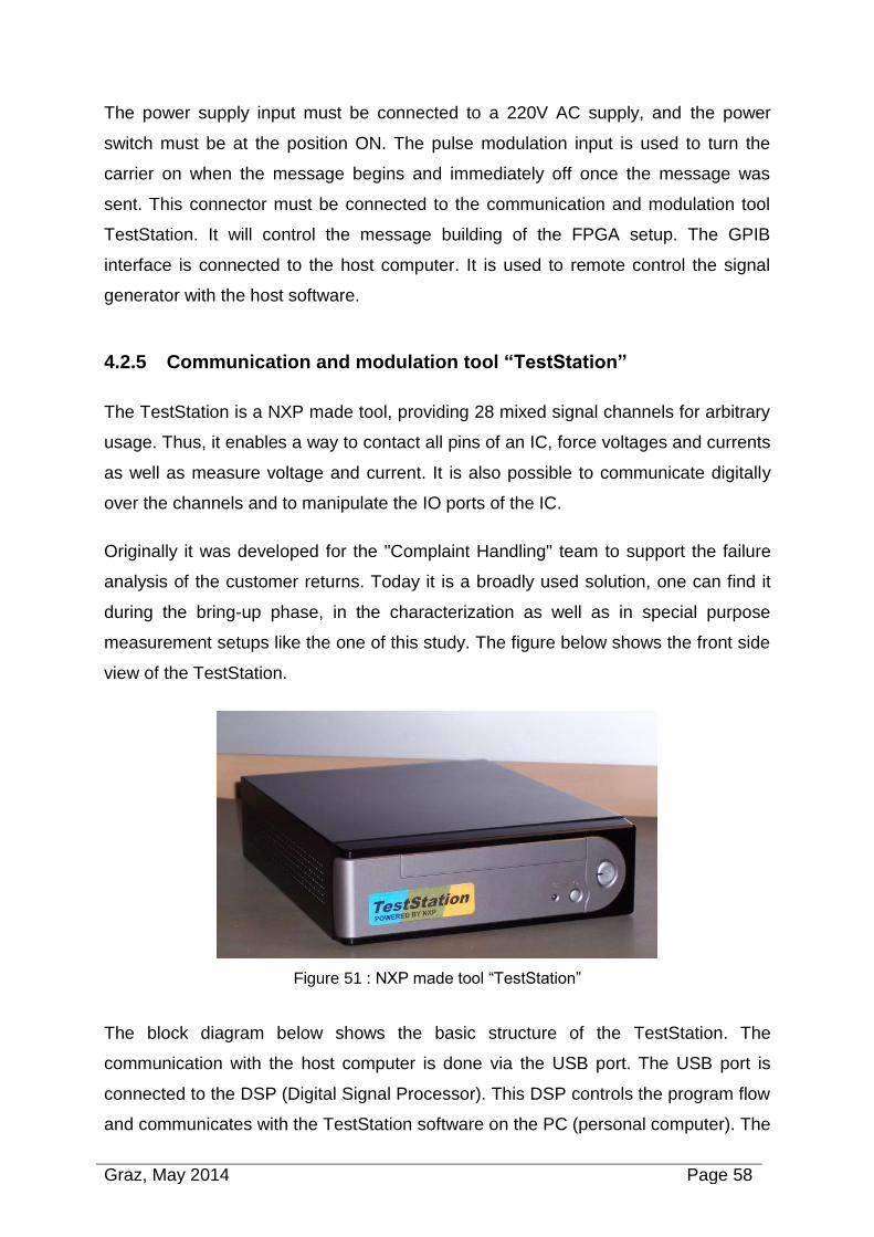
Graz, May 2014 Page 58
The power supply input must be connected to a 220V AC supply, and the power
switch must be at the position ON. The pulse modulation input is used to turn the
carrier on when the message begins and immediately off once the message was
sent. This connector must be connected to the communication and modulation tool
TestStation. It will control the message building of the FPGA setup. The GPIB
interface is connected to the host computer. It is used to remote control the signal
generator with the host software.
4.2.5 Communication and modulation tool “TestStation”
The TestStation is a NXP made tool, providing 28 mixed signal channels for arbitrary
usage. Thus, it enables a way to contact all pins of an IC, force voltages and currents
as well as measure voltage and current. It is also possible to communicate digitally
over the channels and to manipulate the IO ports of the IC.
Originally it was developed for the "Complaint Handling" team to support the failure
analysis of the customer returns. Today it is a broadly used solution, one can find it
during the bring-up phase, in the characterization as well as in special purpose
measurement setups like the one of this study. The figure below shows the front side
view of the TestStation.
Figure 51 : NXP made tool “TestStation”
The block diagram below shows the basic structure of the TestStation. The
communication with the host computer is done via the USB port. The USB port is
connected to the DSP (Digital Signal Processor). This DSP controls the program flow
and communicates with the TestStation software on the PC (personal computer). The
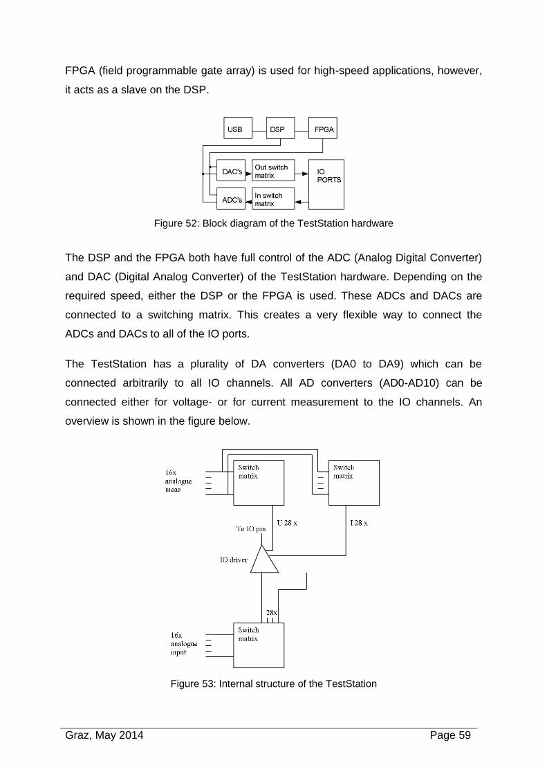
Graz, May 2014 Page 59
FPGA (field programmable gate array) is used for high-speed applications, however,
it acts as a slave on the DSP.
Figure 52: Block diagram of the TestStation hardware
The DSP and the FPGA both have full control of the ADC (Analog Digital Converter)
and DAC (Digital Analog Converter) of the TestStation hardware. Depending on the
required speed, either the DSP or the FPGA is used. These ADCs and DACs are
connected to a switching matrix. This creates a very flexible way to connect the
ADCs and DACs to all of the IO ports.
The TestStation has a plurality of DA converters (DA0 to DA9) which can be
connected arbitrarily to all IO channels. All AD converters (AD0-AD10) can be
connected either for voltage- or for current measurement to the IO channels. An
overview is shown in the figure below.
Figure 53: Internal structure of the TestStation
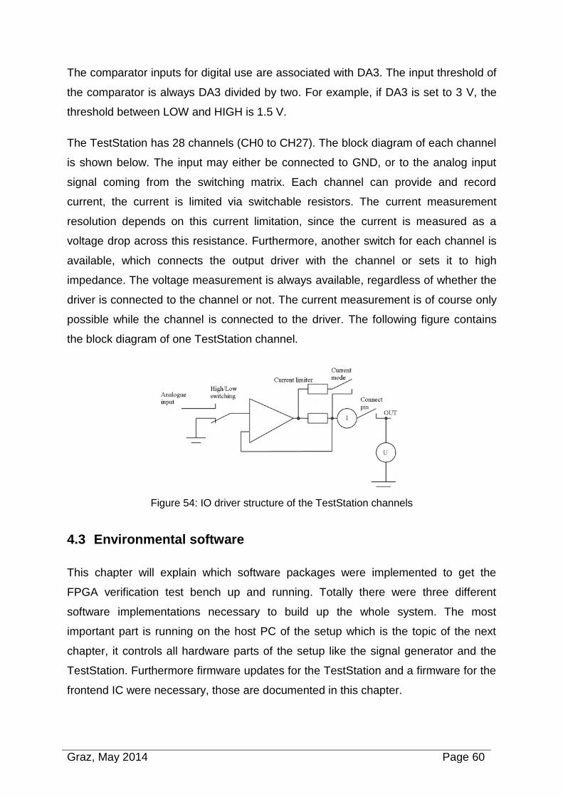
Graz, May 2014 Page 60
The comparator inputs for digital use are associated with DA3. The input threshold of
the comparator is always DA3 divided by two. For example, if DA3 is set to 3 V, the
threshold between LOW and HIGH is 1.5 V.
The TestStation has 28 channels (CH0 to CH27). The block diagram of each channel
is shown below. The input may either be connected to GND, or to the analog input
signal coming from the switching matrix. Each channel can provide and record
current, the current is limited via switchable resistors. The current measurement
resolution depends on this current limitation, since the current is measured as a
voltage drop across this resistance. Furthermore, another switch for each channel is
available, which connects the output driver with the channel or sets it to high
impedance. The voltage measurement is always available, regardless of whether the
driver is connected to the channel or not. The current measurement is of course only
possible while the channel is connected to the driver. The following figure contains
the block diagram of one TestStation channel.
Figure 54: IO driver structure of the TestStation channels
4.3 Environmental software
This chapter will explain which software packages were implemented to get the
FPGA verification test bench up and running. Totally there were three different
software implementations necessary to build up the whole system. The most
important part is running on the host PC of the setup which is the topic of the next
chapter, it controls all hardware parts of the setup like the signal generator and the
TestStation. Furthermore firmware updates for the TestStation and a firmware for the
frontend IC were necessary, those are documented in this chapter.
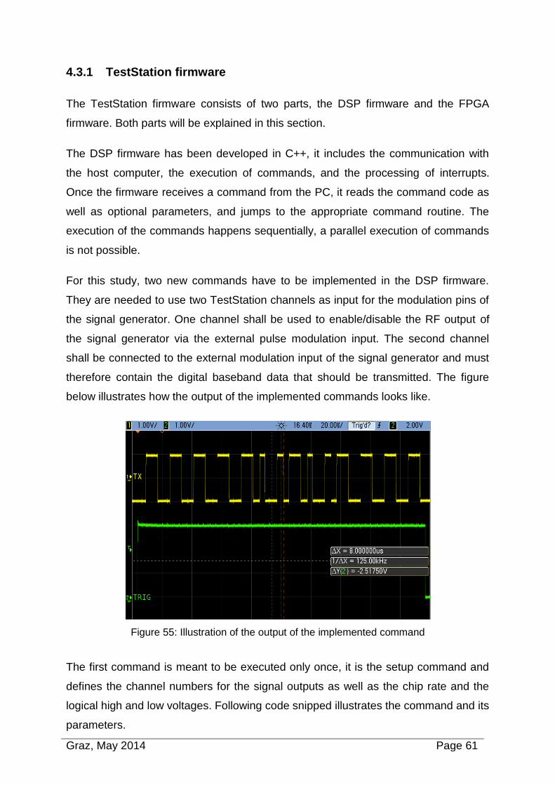
Graz, May 2014 Page 61
4.3.1 TestStation firmware
The TestStation firmware consists of two parts, the DSP firmware and the FPGA
firmware. Both parts will be explained in this section.
The DSP firmware has been developed in C++, it includes the communication with
the host computer, the execution of commands, and the processing of interrupts.
Once the firmware receives a command from the PC, it reads the command code as
well as optional parameters, and jumps to the appropriate command routine. The
execution of the commands happens sequentially, a parallel execution of commands
is not possible.
For this study, two new commands have to be implemented in the DSP firmware.
They are needed to use two TestStation channels as input for the modulation pins of
the signal generator. One channel shall be used to enable/disable the RF output of
the signal generator via the external pulse modulation input. The second channel
shall be connected to the external modulation input of the signal generator and must
therefore contain the digital baseband data that should be transmitted. The figure
below illustrates how the output of the implemented commands looks like.
Figure 55: Illustration of the output of the implemented command
The first command is meant to be executed only once, it is the setup command and
defines the channel numbers for the signal outputs as well as the chip rate and the
logical high and low voltages. Following code snipped illustrates the command and its
parameters.
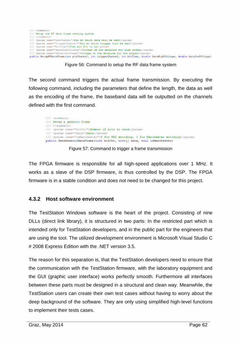
Graz, May 2014 Page 62
Figure 56: Command to setup the RF data frame system
The second command triggers the actual frame transmission. By executing the
following command, including the parameters that define the length, the data as well
as the encoding of the frame, the baseband data will be outputted on the channels
defined with the first command.
Figure 57: Command to trigger a frame transmission
The FPGA firmware is responsible for all high-speed applications over 1 MHz. It
works as a slave of the DSP firmware, is thus controlled by the DSP. The FPGA
firmware is in a stable condition and does not need to be changed for this project.
4.3.2 Host software environment
The TestStation Windows software is the heart of the project. Consisting of nine
DLLs (direct link library), it is structured in two parts: In the restricted part which is
intended only for TestStation developers, and in the public part for the engineers that
are using the tool. The utilized development environment is Microsoft Visual Studio C
# 2008 Express Edition with the .NET version 3.5.
The reason for this separation is, that the TestStation developers need to ensure that
the communication with the TestStation firmware, with the laboratory equipment and
the GUI (graphic user interface) works perfectly smooth. Furthermore all interfaces
between these parts must be designed in a structural and clean way. Meanwhile, the
TestStation users can create their own test cases without having to worry about the
deep background of the software. They are only using simplified high-level functions
to implement their tests cases.
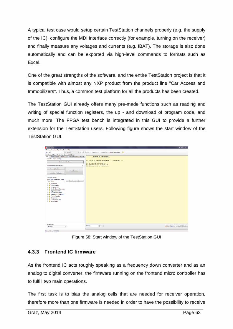
Graz, May 2014 Page 63
A typical test case would setup certain TestStation channels properly (e.g. the supply
of the IC), configure the MDI interface correctly (for example, turning on the receiver)
and finally measure any voltages and currents (e.g. IBAT). The storage is also done
automatically and can be exported via high-level commands to formats such as
Excel.
One of the great strengths of the software, and the entire TestStation project is that it
is compatible with almost any NXP product from the product line "Car Access and
Immobilizers". Thus, a common test platform for all the products has been created.
The TestStation GUI already offers many pre-made functions such as reading and
writing of special function registers, the up - and download of program code, and
much more. The FPGA test bench is integrated in this GUI to provide a further
extension for the TestStation users. Following figure shows the start window of the
TestStation GUI.
Figure 58: Start window of the TestStation GUI
4.3.3 Frontend IC firmware
As the frontend IC acts roughly speaking as a frequency down converter and as an
analog to digital converter, the firmware running on the frontend micro controller has
to fulfill two main operations.
The first task is to bias the analog cells that are needed for receiver operation,
therefore more than one firmware is needed in order to have the possibility to receive
Graz, May 2014 Page 64
at different frequencies. There are three different versions available, one for 315
MHz, one for 434 MHz and one for 925 MHz, as these are the operating bands of the
receiver. The only difference between these different firmware types, is the setup of
the local oscillator which is the input of the IQ mixer.
The second small but very important segment is the output of the ADC stream to port
pins. Three different port pins are necessary for this purpose: ADC_CLK, ADC_I and
ADC_Q. The signals are switched out by a multiplexer that was implemented exactly
for this purpose. This multiplexer is placed directly at the interface between the
analog and the digital part of the receive chain.
The digital receive chain of the frontend IC is in idle state as only the receive chain of
the newest prototype, synthetized in the FPGA shall be tested. Optionally, the receive
chain of the frontend IC could also be activated for a direct comparison with the
FPGA output.
After the necessary configuration, the micro controller of the frontend IC remains in
the idle state as no further operation is necessary. All of the functionality runs
autonomously without any interaction with the CPU.
4.3.4 Backend IC Firmware
For the first version of the FPGA verification setup no firmware for the micro
controller synthetized in the FPGA is necessary. The whole digital receive chain runs
autonomously without any interaction with the CPU needed. All the necessary
operations are handled by the receiver state machine implemented in the digital
receive chain.
4.4 Host software
This chapter will explain which software packages were implemented on the host
computer to get the FPGA verification test bench up and running. The host software
is the most important part of the setup, it controls all hardware parts of the setup like
the signal generator and the TestStation and ensures the correct handling of the
configuration files, the test case execution as well as the result file conversion. In this
chapter all of the implemented functions and test cases are documented.
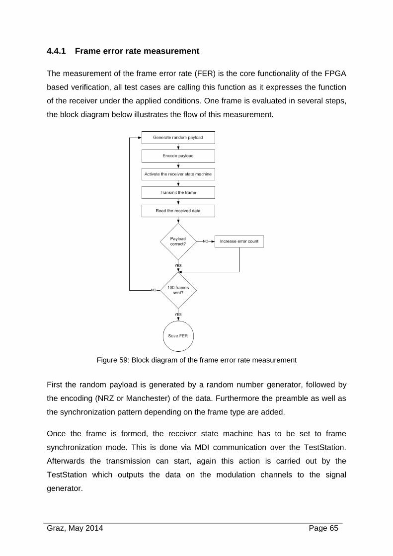
Graz, May 2014 Page 65
4.4.1 Frame error rate measurement
The measurement of the frame error rate (FER) is the core functionality of the FPGA
based verification, all test cases are calling this function as it expresses the function
of the receiver under the applied conditions. One frame is evaluated in several steps,
the block diagram below illustrates the flow of this measurement.
Figure 59: Block diagram of the frame error rate measurement
First the random payload is generated by a random number generator, followed by
the encoding (NRZ or Manchester) of the data. Furthermore the preamble as well as
the synchronization pattern depending on the frame type are added.
Once the frame is formed, the receiver state machine has to be set to frame
synchronization mode. This is done via MDI communication over the TestStation.
Afterwards the transmission can start, again this action is carried out by the
TestStation which outputs the data on the modulation channels to the signal
generator.
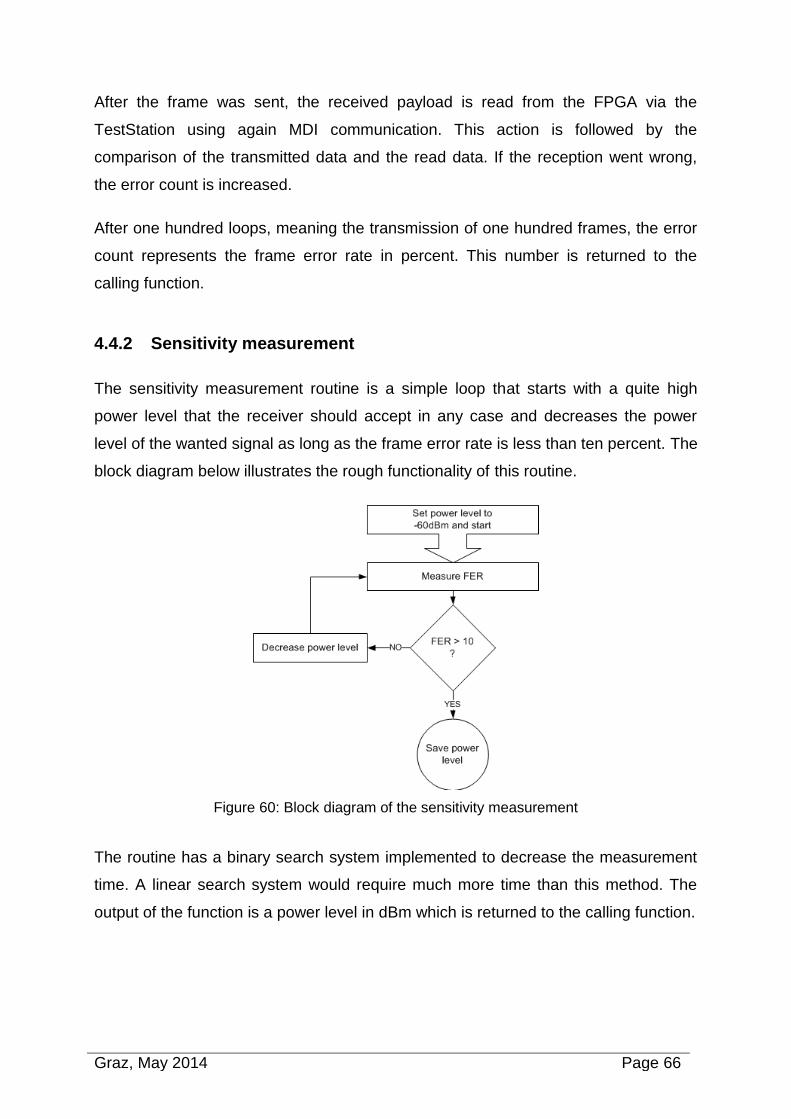
Graz, May 2014 Page 66
After the frame was sent, the received payload is read from the FPGA via the
TestStation using again MDI communication. This action is followed by the
comparison of the transmitted data and the read data. If the reception went wrong,
the error count is increased.
After one hundred loops, meaning the transmission of one hundred frames, the error
count represents the frame error rate in percent. This number is returned to the
calling function.
4.4.2 Sensitivity measurement
The sensitivity measurement routine is a simple loop that starts with a quite high
power level that the receiver should accept in any case and decreases the power
level of the wanted signal as long as the frame error rate is less than ten percent. The
block diagram below illustrates the rough functionality of this routine.
Figure 60: Block diagram of the sensitivity measurement
The routine has a binary search system implemented to decrease the measurement
time. A linear search system would require much more time than this method. The
output of the function is a power level in dBm which is returned to the calling function.
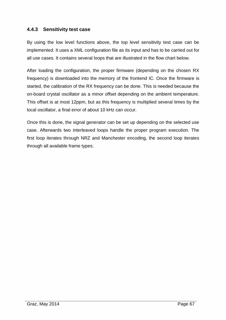
Graz, May 2014 Page 67
4.4.3 Sensitivity test case
By using the low level functions above, the top level sensitivity test case can be
implemented. It uses a XML configuration file as its input and has to be carried out for
all use cases. It contains several loops that are illustrated in the flow chart below.
After loading the configuration, the proper firmware (depending on the chosen RX
frequency) is downloaded into the memory of the frontend IC. Once the firmware is
started, the calibration of the RX frequency can be done. This is needed because the
on-board crystal oscillator as a minor offset depending on the ambient temperature.
This offset is at most 12ppm, but as this frequency is multiplied several times by the
local oscillator, a final error of about 10 kHz can occur.
Once this is done, the signal generator can be set up depending on the selected use
case. Afterwards two interleaved loops handle the proper program execution. The
first loop iterates through NRZ and Manchester encoding, the second loop iterates
through all available frame types.
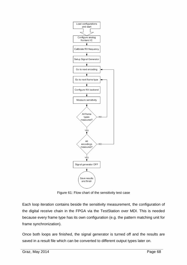
Graz, May 2014 Page 68
Figure 61: Flow chart of the sensitivity test case
Each loop iteration contains beside the sensitivity measurement, the configuration of
the digital receive chain in the FPGA via the TestStation over MDI. This is needed
because every frame type has its own configuration (e.g. the pattern matching unit for
frame synchronization).
Once both loops are finished, the signal generator is turned off and the results are
saved in a result file which can be converted to different output types later on.
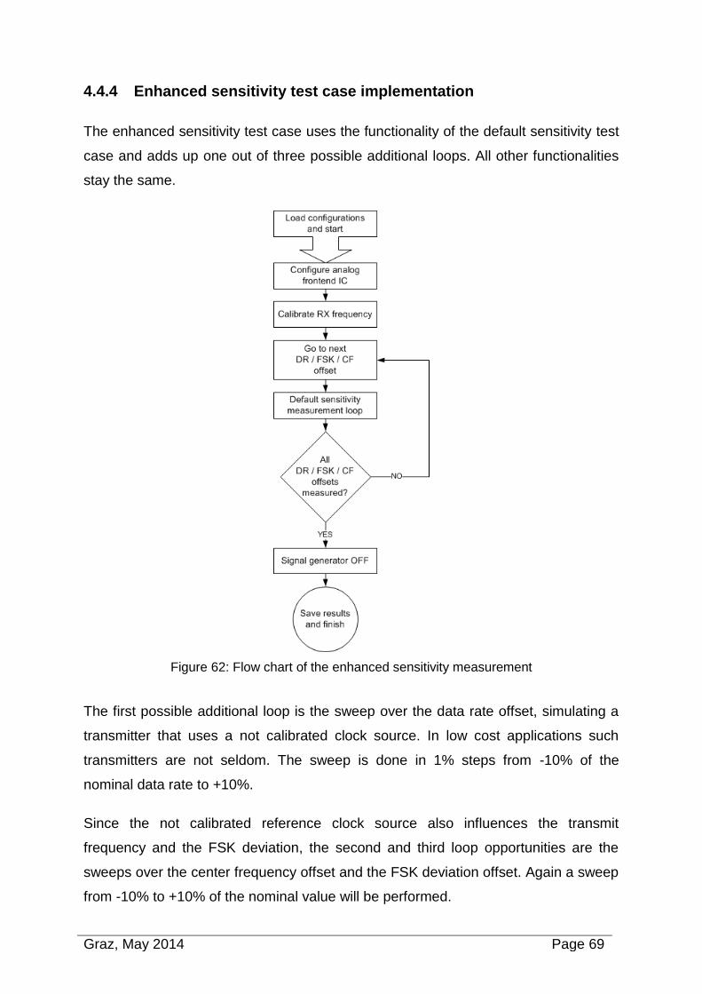
Graz, May 2014 Page 69
4.4.4 Enhanced sensitivity test case implementation
The enhanced sensitivity test case uses the functionality of the default sensitivity test
case and adds up one out of three possible additional loops. All other functionalities
stay the same.
Figure 62: Flow chart of the enhanced sensitivity measurement
The first possible additional loop is the sweep over the data rate offset, simulating a
transmitter that uses a not calibrated clock source. In low cost applications such
transmitters are not seldom. The sweep is done in 1% steps from -10% of the
nominal data rate to +10%.
Since the not calibrated reference clock source also influences the transmit
frequency and the FSK deviation, the second and third loop opportunities are the
sweeps over the center frequency offset and the FSK deviation offset. Again a sweep
from -10% to +10% of the nominal value will be performed.
Graz, May 2014 Page 70
4.4.5 Signal to jammer ratio measurement
The signal to jammer ratio is calculated by the difference of the wanted signal power
level and the jammer power level that causes a frame error rate of ten percent.
Therefore the maximum jammer power must be found, where the frame error rate is
still below ten percent.
The measurement routine is a simple loop that starts with a quite low jammer power
level that the receiver should accept in any case and increases the level of the
jammer as long as the frame error rate is less than ten percent. The block diagram
below illustrates the rough functionality of this routine.
Figure 63: Block diagram of the signal to jammer ratio measurement
Also this routine has a binary search system for test time optimization implemented.
A linear search system would require much more time than this method. The output
of the function is a jammer power level in dBm which is returned to the calling
function. The calling function will calculate the signal to jammer ratio using this value.
4.4.6 Interferer performance test case
By using the low level function above, the top level interferer performance test case
can be implemented. It uses a XML configuration file as its input and has to be
carried out for all use cases. It contains several loops that are illustrated in the flow
chart below.
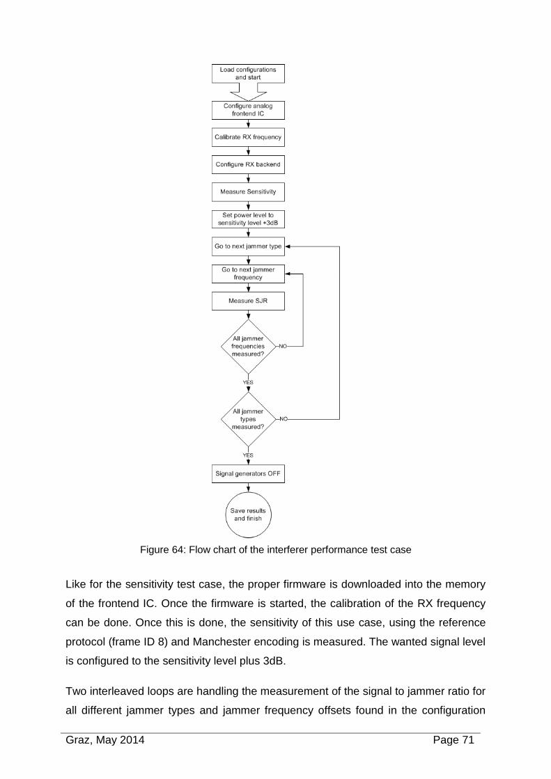
Graz, May 2014 Page 71
Figure 64: Flow chart of the interferer performance test case
Like for the sensitivity test case, the proper firmware is downloaded into the memory
of the frontend IC. Once the firmware is started, the calibration of the RX frequency
can be done. Once this is done, the sensitivity of this use case, using the reference
protocol (frame ID 8) and Manchester encoding is measured. The wanted signal level
is configured to the sensitivity level plus 3dB.
Two interleaved loops are handling the measurement of the signal to jammer ratio for
all different jammer types and jammer frequency offsets found in the configuration
Graz, May 2014 Page 72
file. Once both loops are finished, the signal generators are turned off and the results
are saved in a result file which can be converted to different output types later on.
In the last chapter of this study, one can find a section about possible measurement
time optimizations using a firmware on the backend IC. For further details continue
reading in that section of the study.
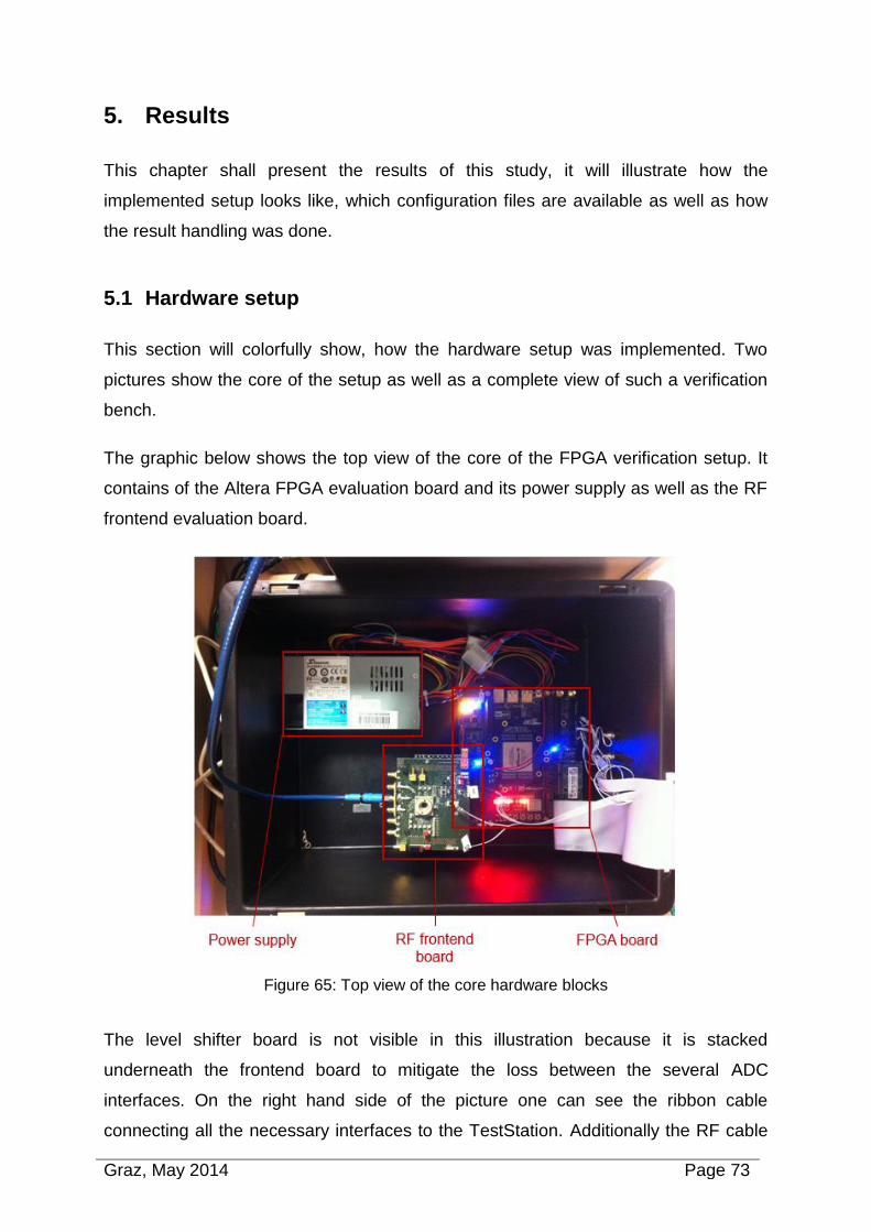
Graz, May 2014 Page 73
5. Results
This chapter shall present the results of this study, it will illustrate how the
implemented setup looks like, which configuration files are available as well as how
the result handling was done.
5.1 Hardware setup
This section will colorfully show, how the hardware setup was implemented. Two
pictures show the core of the setup as well as a complete view of such a verification
bench.
The graphic below shows the top view of the core of the FPGA verification setup. It
contains of the Altera FPGA evaluation board and its power supply as well as the RF
frontend evaluation board.
Figure 65: Top view of the core hardware blocks
The level shifter board is not visible in this illustration because it is stacked
underneath the frontend board to mitigate the loss between the several ADC
interfaces. On the right hand side of the picture one can see the ribbon cable
connecting all the necessary interfaces to the TestStation. Additionally the RF cable
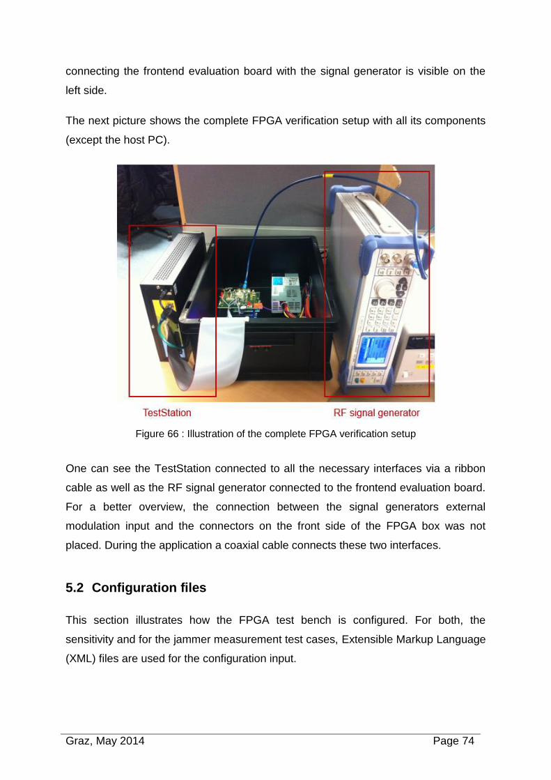
Graz, May 2014 Page 74
connecting the frontend evaluation board with the signal generator is visible on the
left side.
The next picture shows the complete FPGA verification setup with all its components
(except the host PC).
Figure 66 : Illustration of the complete FPGA verification setup
One can see the TestStation connected to all the necessary interfaces via a ribbon
cable as well as the RF signal generator connected to the frontend evaluation board.
For a better overview, the connection between the signal generators external
modulation input and the connectors on the front side of the FPGA box was not
placed. During the application a coaxial cable connects these two interfaces.
5.2 Configuration files
This section illustrates how the FPGA test bench is configured. For both, the
sensitivity and for the jammer measurement test cases, Extensible Markup Language
(XML) files are used for the configuration input.
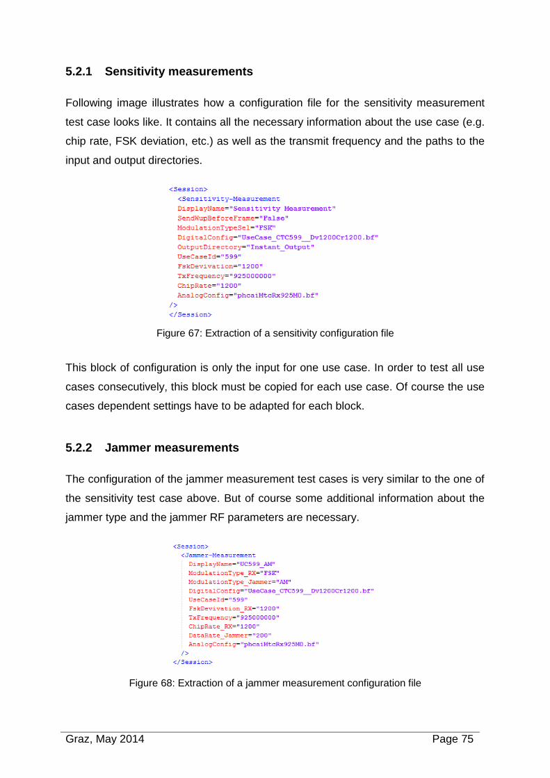
Graz, May 2014 Page 75
5.2.1 Sensitivity measurements
Following image illustrates how a configuration file for the sensitivity measurement
test case looks like. It contains all the necessary information about the use case (e.g.
chip rate, FSK deviation, etc.) as well as the transmit frequency and the paths to the
input and output directories.
Figure 67: Extraction of a sensitivity configuration file
This block of configuration is only the input for one use case. In order to test all use
cases consecutively, this block must be copied for each use case. Of course the use
cases dependent settings have to be adapted for each block.
5.2.2 Jammer measurements
The configuration of the jammer measurement test cases is very similar to the one of
the sensitivity test case above. But of course some additional information about the
jammer type and the jammer RF parameters are necessary.
Figure 68: Extraction of a jammer measurement configuration file
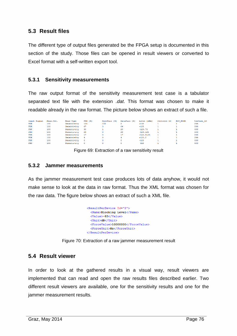
Graz, May 2014 Page 76
5.3 Result files
The different type of output files generated be the FPGA setup is documented in this
section of the study. Those files can be opened in result viewers or converted to
Excel format with a self-written export tool.
5.3.1 Sensitivity measurements
The raw output format of the sensitivity measurement test case is a tabulator
separated text file with the extension .dat. This format was chosen to make it
readable already in the raw format. The picture below shows an extract of such a file.
Figure 69: Extraction of a raw sensitivity result
5.3.2 Jammer measurements
As the jammer measurement test case produces lots of data anyhow, it would not
make sense to look at the data in raw format. Thus the XML format was chosen for
the raw data. The figure below shows an extract of such a XML file.
Figure 70: Extraction of a raw jammer measurement result
5.4 Result viewer
In order to look at the gathered results in a visual way, result viewers are
implemented that can read and open the raw results files described earlier. Two
different result viewers are available, one for the sensitivity results and one for the
jammer measurement results.
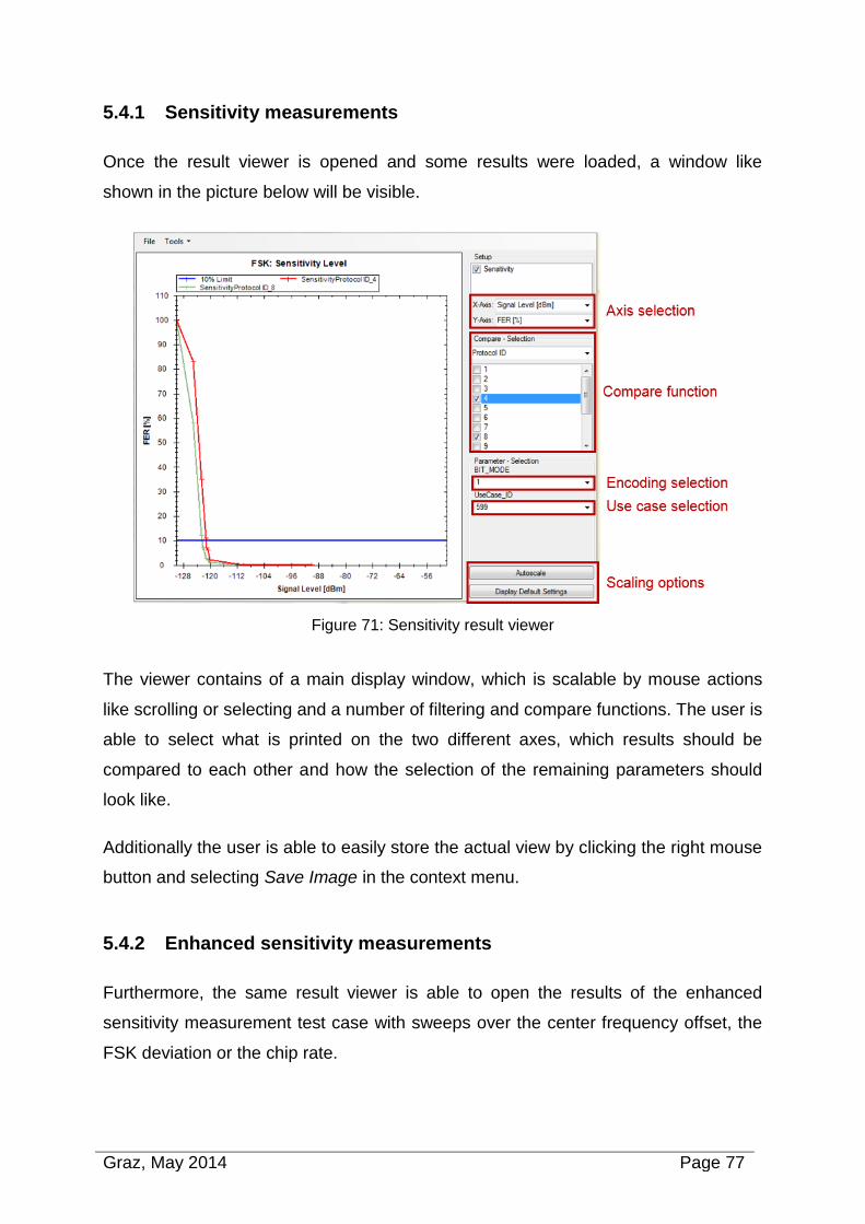
Graz, May 2014 Page 77
5.4.1 Sensitivity measurements
Once the result viewer is opened and some results were loaded, a window like
shown in the picture below will be visible.
Figure 71: Sensitivity result viewer
The viewer contains of a main display window, which is scalable by mouse actions
like scrolling or selecting and a number of filtering and compare functions. The user is
able to select what is printed on the two different axes, which results should be
compared to each other and how the selection of the remaining parameters should
look like.
Additionally the user is able to easily store the actual view by clicking the right mouse
button and selecting Save Image in the context menu.
5.4.2 Enhanced sensitivity measurements
Furthermore, the same result viewer is able to open the results of the enhanced
sensitivity measurement test case with sweeps over the center frequency offset, the
FSK deviation or the chip rate.
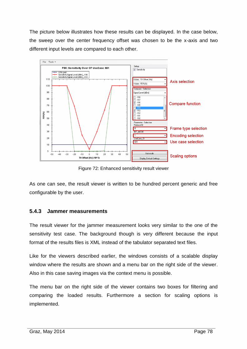
Graz, May 2014 Page 78
The picture below illustrates how these results can be displayed. In the case below,
the sweep over the center frequency offset was chosen to be the x-axis and two
different input levels are compared to each other.
Figure 72: Enhanced sensitivity result viewer
As one can see, the result viewer is written to be hundred percent generic and free
configurable by the user.
5.4.3 Jammer measurements
The result viewer for the jammer measurement looks very similar to the one of the
sensitivity test case. The background though is very different because the input
format of the results files is XML instead of the tabulator separated text files.
Like for the viewers described earlier, the windows consists of a scalable display
window where the results are shown and a menu bar on the right side of the viewer.
Also in this case saving images via the context menu is possible.
The menu bar on the right side of the viewer contains two boxes for filtering and
comparing the loaded results. Furthermore a section for scaling options is
implemented.
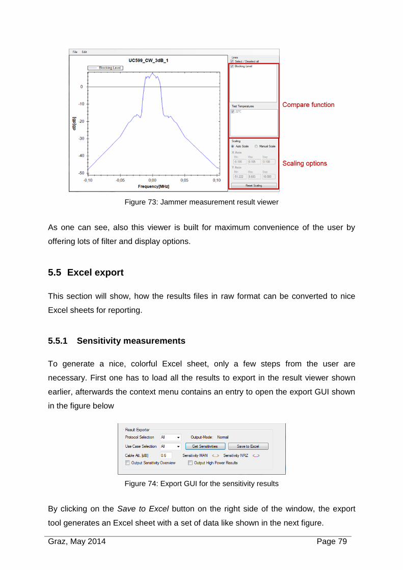
Graz, May 2014 Page 79
Figure 73: Jammer measurement result viewer
As one can see, also this viewer is built for maximum convenience of the user by
offering lots of filter and display options.
5.5 Excel export
This section will show, how the results files in raw format can be converted to nice
Excel sheets for reporting.
5.5.1 Sensitivity measurements
To generate a nice, colorful Excel sheet, only a few steps from the user are
necessary. First one has to load all the results to export in the result viewer shown
earlier, afterwards the context menu contains an entry to open the export GUI shown
in the figure below
Figure 74: Export GUI for the sensitivity results
By clicking on the Save to Excel button on the right side of the window, the export
tool generates an Excel sheet with a set of data like shown in the next figure.
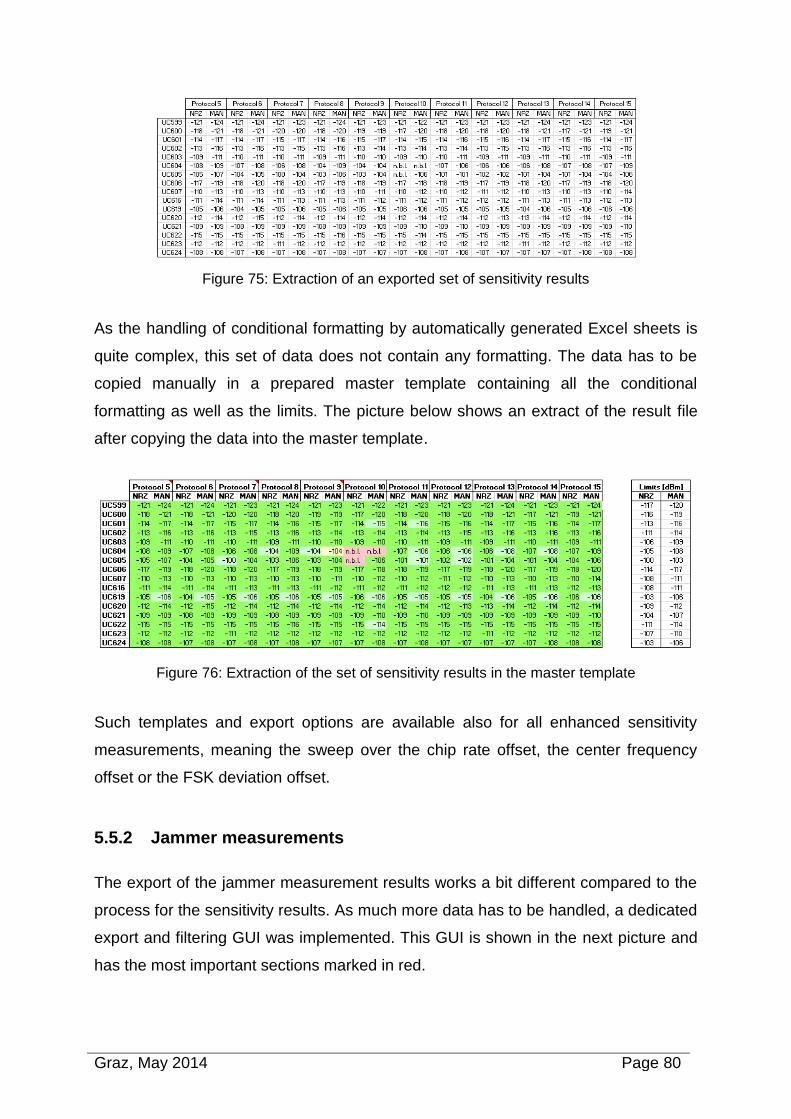
Graz, May 2014 Page 80
Figure 75: Extraction of an exported set of sensitivity results
As the handling of conditional formatting by automatically generated Excel sheets is
quite complex, this set of data does not contain any formatting. The data has to be
copied manually in a prepared master template containing all the conditional
formatting as well as the limits. The picture below shows an extract of the result file
after copying the data into the master template.
Figure 76: Extraction of the set of sensitivity results in the master template
Such templates and export options are available also for all enhanced sensitivity
measurements, meaning the sweep over the chip rate offset, the center frequency
offset or the FSK deviation offset.
5.5.2 Jammer measurements
The export of the jammer measurement results works a bit different compared to the
process for the sensitivity results. As much more data has to be handled, a dedicated
export and filtering GUI was implemented. This GUI is shown in the next picture and
has the most important sections marked in red.
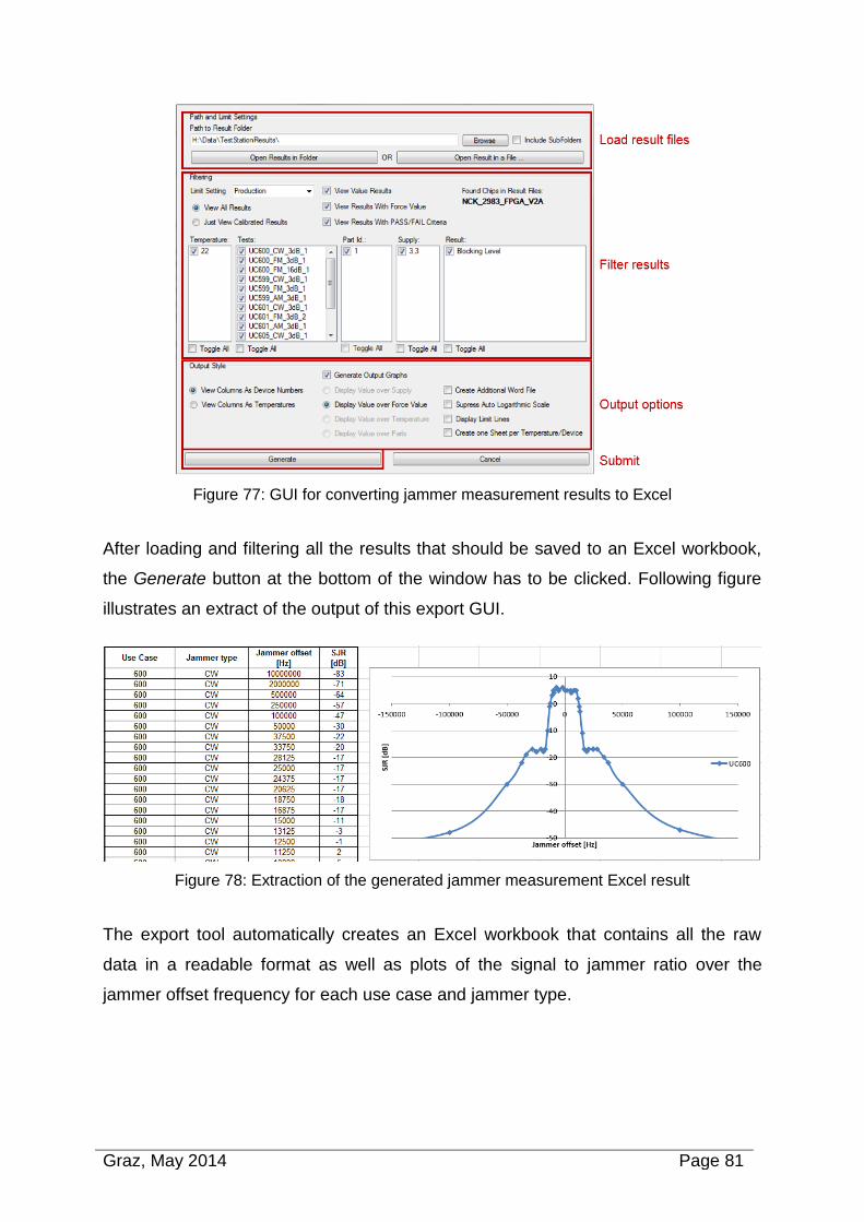
Graz, May 2014 Page 81
Figure 77: GUI for converting jammer measurement results to Excel
After loading and filtering all the results that should be saved to an Excel workbook,
the Generate button at the bottom of the window has to be clicked. Following figure
illustrates an extract of the output of this export GUI.
Figure 78: Extraction of the generated jammer measurement Excel result
The export tool automatically creates an Excel workbook that contains all the raw
data in a readable format as well as plots of the signal to jammer ratio over the
jammer offset frequency for each use case and jammer type.
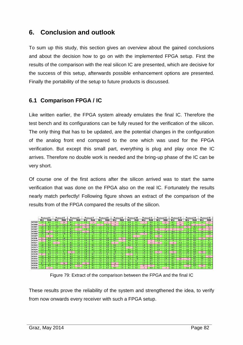
Graz, May 2014 Page 82
6. Conclusion and outlook
To sum up this study, this section gives an overview about the gained conclusions
and about the decision how to go on with the implemented FPGA setup. First the
results of the comparison with the real silicon IC are presented, which are decisive for
the success of this setup, afterwards possible enhancement options are presented.
Finally the portability of the setup to future products is discussed.
6.1 Comparison FPGA / IC
Like written earlier, the FPGA system already emulates the final IC. Therefore the
test bench and its configurations can be fully reused for the verification of the silicon.
The only thing that has to be updated, are the potential changes in the configuration
of the analog front end compared to the one which was used for the FPGA
verification. But except this small part, everything is plug and play once the IC
arrives. Therefore no double work is needed and the bring-up phase of the IC can be
very short.
Of course one of the first actions after the silicon arrived was to start the same
verification that was done on the FPGA also on the real IC. Fortunately the results
nearly match perfectly! Following figure shows an extract of the comparison of the
results from of the FPGA compared the results of the silicon.
Figure 79: Extract of the comparison between the FPGA and the final IC
These results prove the reliability of the system and strengthened the idea, to verify
from now onwards every receiver with such a FPGA setup.
Graz, May 2014 Page 83
6.2 Capturing of ADC streams
For test and debugging purposes the FPGA implementation has been enhanced by a
special recording and playback mechanism that allows in-system injection and
monitoring of a set of pre-defined signals. Although the development of this feature
originally was intended to be used for the spread spectrum sub-block (DSSS), it
could also be re-used for injection of the ADC I & Q data streams, as well as for
recording of the receive debug bus. In addition, a Quartus Signaltap [22] core has
been inserted for tracking of various important signals, e.g. CPU program counter,
ports, interrupt signals, etc.
All these functionalities are already available in the FPGA implementation and could
be accessed by the host software. One possible implementation could be, that the
TestStation is used to trigger the recording of the ADC I & Q data streams via an IO
channel. Afterwards the host software could read out the recorded stream and
display it visually in a nice GUI on the host PC. This would enable lots of additional
debugging functionalities if one would like to know why dedicated frames cannot be
correctly demodulated by the receive chain.
6.3 Measurement time optimizations
As the available time for the verification of a receiver before the design freeze
happens is always very limited, the measurement time is the key to success. If the
time to measure the frame error rate can be reduced, the measurement coverage
can be even increased without increasing the verification time.
One possible option would be to transfer a part of the frame error rate measurement
into a firmware which is executed by the micro controller synthetized in the FPGA. A
big time consumer is the communication with the IC before and after each frame. The
actual system is built in a way that the received payload is read out after each sent
frame. This is needed for the comparison of the sent data with the received data. As
the communication speed is quite low and also the number of TestStation commands
needed is high and furthermore hundreds of frames have to be sent until the
sensitivity limit is distinguished, this takes quite a long time.
Graz, May 2014 Page 84
If all the payloads that are going to be sent are passed to the firmware of the IC
before the transmission starts and the comparison of the received payload with the
sent data is done internally by the micro controller, the measurement time could be
reduced tremendously. The number of communications between the TestStation and
the IC in the FPGA would be reduced heavily which saves a lot of measurement time.
Furthermore a smart way of detecting the sensitivity level could be introduced.
Actually a static number of one hundred frames is sent per power level to check if the
frame error rate is above or below ten percent. But if all or no frames are correctly
demodulated, ten frames also would have been enough to take the right decision.
Only in the range of the sensitivity limit plus minus 3dB one hundred frames are
necessary to get an accurate result. By implementing such a smart way of measuring
the frame error rate efficiently, a lot of wasted time can be saved.
6.4 Portability to future prototypes
Like written in previous chapters. the prerequisite of such a FPGA based verification
is of course, that the analog front end of the receiver to be verified is either already
available on a test chip, or does not change tremendously compared to the previous
version of the receiver. This is the case because a verification of the digital part of the
receiver makes no sense, if the analog part (e.g. the Sigma Delta ADC) changes
dramatically. Aim of the FPGA based verification is to test the whole system, frontend
as well as backend.
Luckily NXP will never tape a completely new product without carrying out the
verification on a test chip before, especially if lots of hardware IPs change. The only
exception is, if a product differs only in a few aspects compared to the previous one,
in that case a test chip verification can be disclaimed. In both cases, a frontend IC for
a FPGA verification is available. Therefore this kind of verification of the digital
receive chain can be carried out for all future types of NXPs receivers.
As the verification of the receiver for which the setup was built, was very successful,
already two more receiver versions were ported to the FPGA test bench. One of them
is also already finished successfully, the second one is actually in progress.
Graz, May 2014 Page 85
References
1. NXP, ATIC134 Medium Datasheet. 2013.
2. Friis, H.T. and J.R. Pierce, The Wisdom of Harald Friis. 1957.
3. Friis, H.T., Noise Figures of Radio Receivers. Proceedings of the IRE, 1944. 32(7): p. 419-422.
4. Sabah, S. and R. Lorenz. Design and calibration of IQ-Mixers. in EPAC. 1998.
5. Tietze, U. and C. Schenk, Halbleiter-Schaltungstechnik: [neuer Teil: Nachrichtentechnische Schaltungen]. 2002: Springer.
6. Schreier, R. and G.C. Temes, Understanding Delta-Sigma Data Converters. 2004: Wiley.
7. Söderkvist, S., Tidsdiskreta system: Exempelsamling. 1980.
8. Pirsch, P., Architekturen der digitalen Signalverarbeitung. 1996: Teubner.
9. Smith, S.W., The scientist and engineer's guide to digital signal processing. 1997: California Technical Publishing. 625.
10. Bakshi, A.P.G.U.A., Analog Integrated Circuits - Design And Applications. 2009: Technical Publications.
11. North, D.O., An Analysis of the factors which determine signal/noise discrimination in pulsed-carrier systems. Proceedings of the IEEE, 1963. 51(7): p. 1016-1027.
12. Turin, G.L., An introduction to matched filters. Information Theory, IRE Transactions on, 1960. 6(3): p. 311-329.
13. Sklar, B., Digital communications: fundamentals and applications. 2001: Prentice-Hall PTR.
14. ETSI, Electromagnetic compatibility and Radio spectrum Matters (ERM);Short Range Devices (SRD);Radio equipment to be used in the 25 MHz to 1 000 MHz frequency range with power levels ranging up to 500 mW;Part 1: Technical characteristics and test methods. 2012.
15. Gu, Q., RF System Design of Transceivers for Wireless Communications. 2005: Springer.
16. Hickman, I., Practical RF Handbook. 2006: Elsevier Science.
17. Altera, Cyclone II Architecture. 2007.
18. Betz, V. FPGA Architecture for the Challenge. Available from: http://www.eecg.toronto.edu/~vaughn/challenge/fpga_arch.html.
19. Wolf, W., FPGA-Based System Design. 2004: Pearson Education.
Graz, May 2014 Page 86
20. Altera, Stratix III FPGA: Lowest Power, Highest Performance 65- nm FPGA.
21. Schwarz, R., R&S SMB100A Operating Manual.
22. Altera, Quartus II Handbook Version 13.1. 2013.
Graz, May 2014 Page 87
List of Figures
Figure 1: Full receive chain [1] .................................................................................... 9
Figure 2: Analog Frontend [1] ................................................................................... 10
Figure 3: IQ Mixer [4] ................................................................................................ 11
Figure 4: Transimpedance amplifier [5] .................................................................... 12
Figure 5: Block diagram of a first order SD ADC [1] ................................................. 14
Figure 6: Block diagram of the IF preprocessing [1] ................................................. 14
Figure 7: Decimation filter with lowpass filter followed by down sampling [7] ........... 15
Figure 8: Lowpass filter with a cut off frequency of π/M [7] ...................................... 15
Figure 9: Example of a decimated signal [7] ............................................................. 16
Figure 10: DC notch filter response [8] ..................................................................... 16
Figure 11: Block diagram of the narrowband receive chain [1] ................................. 18
Figure 12: CORDIC algorithm process [8] ................................................................ 18
Figure 13: Ideal low pass filter [9] ............................................................................. 19
Figure 14: Impulse response of ideal LPF [9] ........................................................... 20
Figure 15: Filter weights M=20, ft=0.23 [9] ............................................................... 20
Figure 16: Formulas to calculate the filter weights [9] ............................................... 21
Figure 17: Frequency response of a real LPF using a rectangular window [9] ......... 21
Figure 18: Comparison of Hamming window and rectangular window [9] ................ 21
Figure 19 : BLock Diagram of a FSK Demodulation PLL [1] ..................................... 23
Figure 20: Transmitted data without additive white Gaussian noise [12] .................. 24
Figure 21: Received data with additive white Gaussian noise [12] ........................... 24
Figure 22: Received data after the matched filter [12] .............................................. 25
Figure 23: Sample points on the received signal [12] ............................................... 25
Figure 24: Block diagram of the clock data recovery [1] ........................................... 25
Figure 25: Block diagram of the MRK3 CPU [1] ....................................................... 28
Figure 26: Illustration of a typical MDI command including a response of the IC ...... 30
Figure 27: BER measurement setup ........................................................................ 32
Figure 28: Test Message for FER Measurement ...................................................... 33
Graz, May 2014 Page 88
Figure 29: Timing of Test Message .......................................................................... 34
Figure 30: FER measurement setup ......................................................................... 34
Figure 31 : Jammer measurement setup .................................................................. 35
Figure 32: Principle of the interferer measurement ................................................... 36
Figure 33: Position of ACR interferer ........................................................................ 37
Figure 34: Position of Co-Channel interferer ............................................................ 38
Figure 35: Illustration of the IRR measurement ........................................................ 38
Figure 36: Position of the image interferer ................................................................ 39
Figure 37: Position of the blocking interferer ............................................................ 40
Figure 38: Illustration of a spurious response measurement .................................... 41
Figure 39 : FSK modulation principle [13] ................................................................. 42
Figure 40: ASK modulation principle [13].................................................................. 42
Figure 41: Block diagram of a configurable logic block [17] ...................................... 45
Figure 42: Connections in a switch box [18] ............................................................. 45
Figure 43: Block diagram of the FPGA implementation ............................................ 50
Figure 44: Clock and reset generation ...................................................................... 50
Figure 45: Block diagram of the hardware setup ...................................................... 52
Figure 46 : RF frontend evaluation board ................................................................. 54
Figure 47: Schematic of the level shifter board ......................................................... 55
Figure 48: Terasic DE3-150 board ........................................................................... 55
Figure 49: Front panel of the SMB100A signal generator [21] .................................. 57
Figure 50: Rear panel of the SMB100A signal generator [21] .................................. 57
Figure 51 : NXP made tool “TestStation” .................................................................. 58
Figure 52: Block diagram of the TestStation hardware ............................................. 59
Figure 53: Internal structure of the TestStation ......................................................... 59
Figure 54: IO driver structure of the TestStation channels ........................................ 60
Figure 55: Illustration of the output of the implemented command ........................... 61
Figure 56: Command to setup the RF data frame system ........................................ 62
Figure 57: Command to trigger a frame transmission ............................................... 62
Figure 58: Start window of the TestStation GUI ........................................................ 63
Graz, May 2014 Page 89
Figure 59: Block diagram of the frame error rate measurement ............................... 65
Figure 60: Block diagram of the sensitivity measurement......................................... 66
Figure 61: Flow chart of the sensitivity test case ...................................................... 68
Figure 62: Flow chart of the enhanced sensitivity measurement .............................. 69
Figure 63: Block diagram of the signal to jammer ratio measurement ...................... 70
Figure 64: Flow chart of the interferer performance test case .................................. 71
Figure 65: Top view of the core hardware blocks ..................................................... 73
Figure 66 : Illustration of the complete FPGA verification setup ............................... 74
Figure 67: Extraction of a sensitivity configuration file .............................................. 75
Figure 68: Extraction of a jammer measurement configuration file ........................... 75
Figure 69: Extraction of a raw sensitivity result ......................................................... 76
Figure 70: Extraction of a raw jammer measurement result ..................................... 76
Figure 71: Sensitivity result viewer ........................................................................... 77
Figure 72: Enhanced sensitivity result viewer ........................................................... 78
Figure 73: Jammer measurement result viewer ........................................................ 79
Figure 74: Export GUI for the sensitivity results ........................................................ 79
Figure 75: Extraction of an exported set of sensitivity results ................................... 80
Figure 76: Extraction of the set of sensitivity results in the master template ............. 80
Figure 77: GUI for converting jammer measurement results to Excel ...................... 81
Figure 78: Extraction of the generated jammer measurement Excel result .............. 81
Figure 79: Extract of the comparison between the FPGA and the final IC ................ 82
Figure 80 : Schematic of the RF frontend evaluation board...................................... 91
Graz, May 2014 Page 90
List of Tables
Table 1: Channel filter selection ............................................................................... 22
Table 2 : Use case overview ..................................................................................... 31
Table 3: Message protocol overview ........................................................................ 33
Table 4 : Channel separation for each channel filter bandwidth ............................... 37
Table 5 : Implemented memories ............................................................................. 51
Table 6: Necessary tools to implement a FPGA-ready bit stream ............................ 51
Table 7 : Detailed pinout of the FPGA evaluation board ........................................... 92
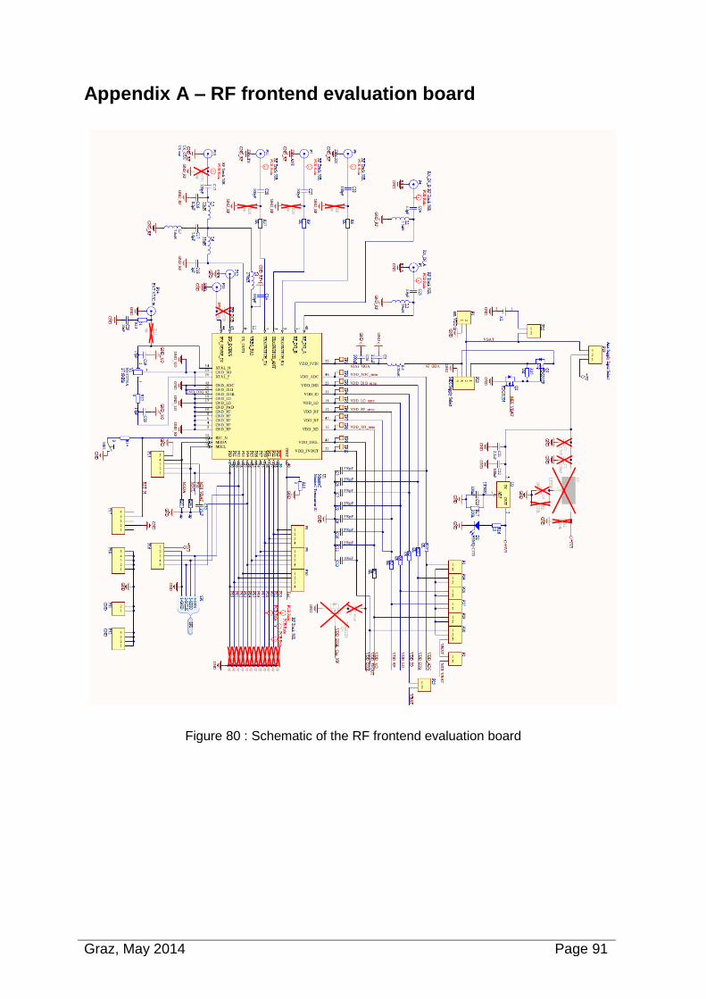
Graz, May 2014 Page 91
Appendix A – RF frontend evaluation board
Figure 80 : Schematic of the RF frontend evaluation board
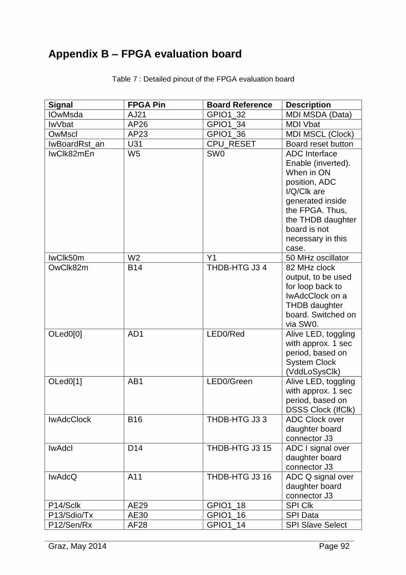
Graz, May 2014 Page 92
Appendix B – FPGA evaluation board
Table 7 : Detailed pinout of the FPGA evaluation board
Signal FPGA Pin Board Reference Description
IOwMsda AJ21 GPIO1_32 MDI MSDA (Data)
IwVbat AP26 GPIO1_34 MDI Vbat
OwMscl AP23 GPIO1_36 MDI MSCL (Clock)
IwBoardRst_an U31 CPU_RESET Board reset button
IwClk82mEn W5 SW0 ADC Interface Enable (inverted). When in ON position, ADC I/Q/Clk are generated inside the FPGA. Thus, the THDB daughter board is not necessary in this case.
IwClk50m W2 Y1 50 MHz oscillator
OwClk82m B14 THDB-HTG J3 4 82 MHz clock output, to be used for loop back to IwAdcClock on a THDB daughter board. Switched on via SW0.
OLed0[0] AD1 LED0/Red Alive LED, toggling with approx. 1 sec period, based on System Clock (VddLoSysClk)
OLed0[1] AB1 LED0/Green Alive LED, toggling with approx. 1 sec period, based on DSSS Clock (IfClk)
IwAdcClock B16 THDB-HTG J3 3 ADC Clock over daughter board connector J3
IwAdcI D14 THDB-HTG J3 15 ADC I signal over daughter board connector J3
IwAdcQ A11 THDB-HTG J3 16 ADC Q signal over daughter board connector J3
P14/Sclk AE29 GPIO1_18 SPI Clk
P13/Sdio/Tx AE30 GPIO1_16 SPI Data
P12/Sen/Rx AF28 GPIO1_14 SPI Slave Select
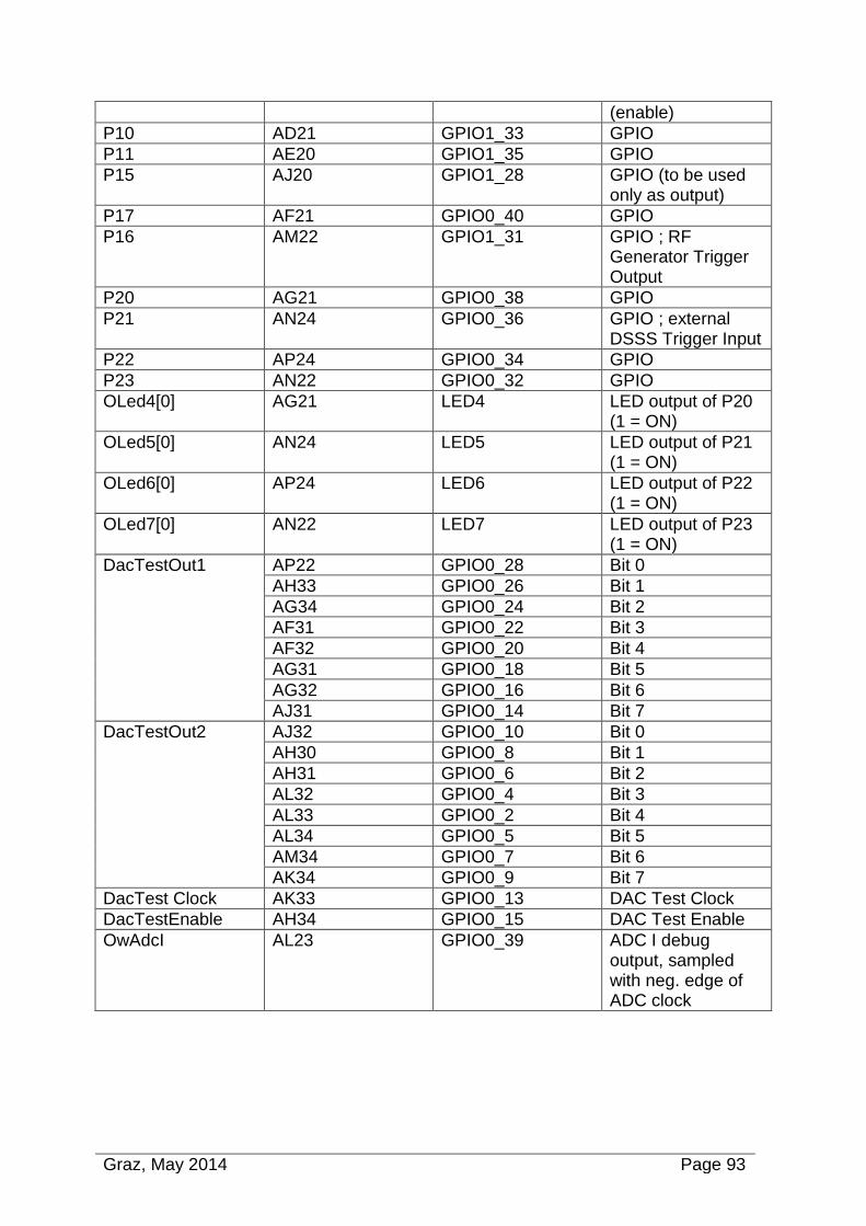
Graz, May 2014 Page 93
(enable)
P10 AD21 GPIO1_33 GPIO
P11 AE20 GPIO1_35 GPIO
P15 AJ20 GPIO1_28 GPIO (to be used only as output)
P17 AF21 GPIO0_40 GPIO
P16 AM22 GPIO1_31 GPIO ; RF Generator Trigger Output
P20 AG21 GPIO0_38 GPIO
P21 AN24 GPIO0_36 GPIO ; external DSSS Trigger Input
P22 AP24 GPIO0_34 GPIO
P23 AN22 GPIO0_32 GPIO
OLed4[0] AG21 LED4 LED output of P20 (1 = ON)
OLed5[0] AN24 LED5 LED output of P21 (1 = ON)
OLed6[0] AP24 LED6 LED output of P22 (1 = ON)
OLed7[0] AN22 LED7 LED output of P23 (1 = ON)
DacTestOut1 AP22 GPIO0_28 Bit 0
AH33 GPIO0_26 Bit 1
AG34 GPIO0_24 Bit 2
AF31 GPIO0_22 Bit 3
AF32 GPIO0_20 Bit 4
AG31 GPIO0_18 Bit 5
AG32 GPIO0_16 Bit 6
AJ31 GPIO0_14 Bit 7
DacTestOut2 AJ32 GPIO0_10 Bit 0
AH30 GPIO0_8 Bit 1
AH31 GPIO0_6 Bit 2
AL32 GPIO0_4 Bit 3
AL33 GPIO0_2 Bit 4
AL34 GPIO0_5 Bit 5
AM34 GPIO0_7 Bit 6
AK34 GPIO0_9 Bit 7
DacTest Clock AK33 GPIO0_13 DAC Test Clock
DacTestEnable AH34 GPIO0_15 DAC Test Enable
OwAdcI AL23 GPIO0_39 ADC I debug output, sampled with neg. edge of ADC clock