Embed Size (px)
Citation preview
SURFACE AND INTERFACE ANALYSIS, VOL. 25, 488È491 (1997)
Fractal Dimension of Thin-Ðlm Surfaces Obtainedby Fourier Spectral Analysis
W. Zahn and A. Zo� sch*Westsa� chsische Hochschule Zwickau, Fachbereich Physikalische Technik/Informatik, Dr. Friedrichs-Ring 2A, 08056 Zwickau,Germany
The applicability of models based on fractal geometry to characterize thin-Ðlm surfaces was investigated. Thefractal geometry of sputtered chromium nitride and silicon nitride thin-Ðlm surfaces was described using Fourierspectral analysis of proÐles from scanning tunnelling microscopy images and atomic force microscopy images.
The and coatings were deposited on silicon wafers using reactive magnetron sputtering and varyingCrNx
SiNxthe gas pressure. The columnar structure of the amorphous silicon nitride varied with deposition, similar to the
structure of the polycrystalline chromium nitride Ðlms.The fractal dimension decreases with increasing pressure. Films with Ðne columnar structures are characterized
by a larger fractal dimension than Ðlms with coarse columnar structures. 1997 by John Wiley & Sons, Ltd.(
Surf. Interface Anal. 25, 488È491 (1997)No. of Figures : 5 No. of Tables : 0 No. of Refs : 11
KEYWORDS: fractal dimension ; Fourier spectral analysis ; STM; AFM; thin Ðlms ; magnetron sputtering
INTRODUCTION
The behaviour of the surface structure of thin Ðlms is ofgreat interest for many applications of microelectronics,optics and micromechanics.
The irregular shape of thin-Ðlm surfaces requires newmethods for description. Recently, the concept of fractaldimension has been used to describe the statisticalbehaviour of thin-Ðlm surfaces.1h5 Fractal descriptionscharacterize surfaces by a non-integer dimension, calledthe fractal dimension, which di†ers from the topologicaldimension. In order to determine fractal dimensionsseveral methods have been developed, obtaining severalresults. Typical dimensions are the box dimension, thesimilarity dimension, the Hausdor† dimension and thespectral density. The several dimensions may be equalor related through simple expressions. The mostcommon methods to determine fractal dimension arethe box counting method and Fourier proÐle analysis.It has been shown that Fourier proÐle analysis is the moreaccurate method for statistically self-affine structures.
The structure of coatings depends on many factors,especially the deposition conditions. Investigations intothe dependence of the fractal dimension on the deposi-tion parameters show the applicability of fractal modelsto qualitative and quantitative descriptions of sputteredthin-Ðlm surfaces.
EXPERIMENTAL CONDITIONS
The investigated and coatings were depos-CrNx
SiNxited on SiS111T wafers using a planar magnetron with a
* Correspondence to : A. Zo� sch, Westsa� chsische HochschuleZwickau, Fachbereich Physikalische Technik/Informatik, Dr.Friedrichs-Ring 2A, 08056 Zwickau, Germany.
ring-shaped target in a d.c. discharge with argon as thesputtering gas.6,7 The working gas pressure was variedin the range 0.27È2.25 Pa.
Other parameters, such as power, substrate tem-perature, relation of partial pressures of argon andnitrogen and geometry of the deposition device, wereinvariable.
For silicon nitride the part of nitrogen in the workinggas was 64%. In this case the coatings are amorp-SiN
xhous with x \ 1.44. The substrate temperature amount-ed to 470 K. The chromium nitride coatings weredeposited with a partial pressure relation ofpN2/pAr25%. X-ray di†raction analysis shows a mixture of CrNand in this range. The amount of nitrogen in theCr2Ncoatings was 43 at.% (EDX analysis). The depositiontemperature amounted to 530 K.
The surfaces of the samples were analysed by scan-ning tunnelling microscopy (STM). The measurementswere carried out in constant current mode (0.2 nA; 0.4V) using a gold tip. Thereby, the insulating layers weredeposited with a thin sputtered gold layer (power \ 6.6W; pressure \ 5 mbar ; target-substrate distance \ 4cm; time \ 8 min). The same procedure was applied forall the samples.
For comparison, surface images of the samples wereproduced by atomic force microscopy (AFM) too. The
coatings were measured in contact mode. In theCrNxcase of very hard coatings, being extremely insu-SiN
xlating, the better results were received by measurementsin non-contact mode.
FOURIER SPECTRAL ANALYSIS
For characterizing the Ðlm surfaces the fractal dimen-sion has been determined by Fourier analysis. ProÐleswere extracted from the STM and AFM image Ðles as a
CCC 0142È2421/97/070488È04 $17.50 Received 16 September 1996( 1997 by John Wiley & Sons, Ltd. Accepted 6 February 1997
FRACTAL DIMENSION OF THIN-FILM SURFACES 489
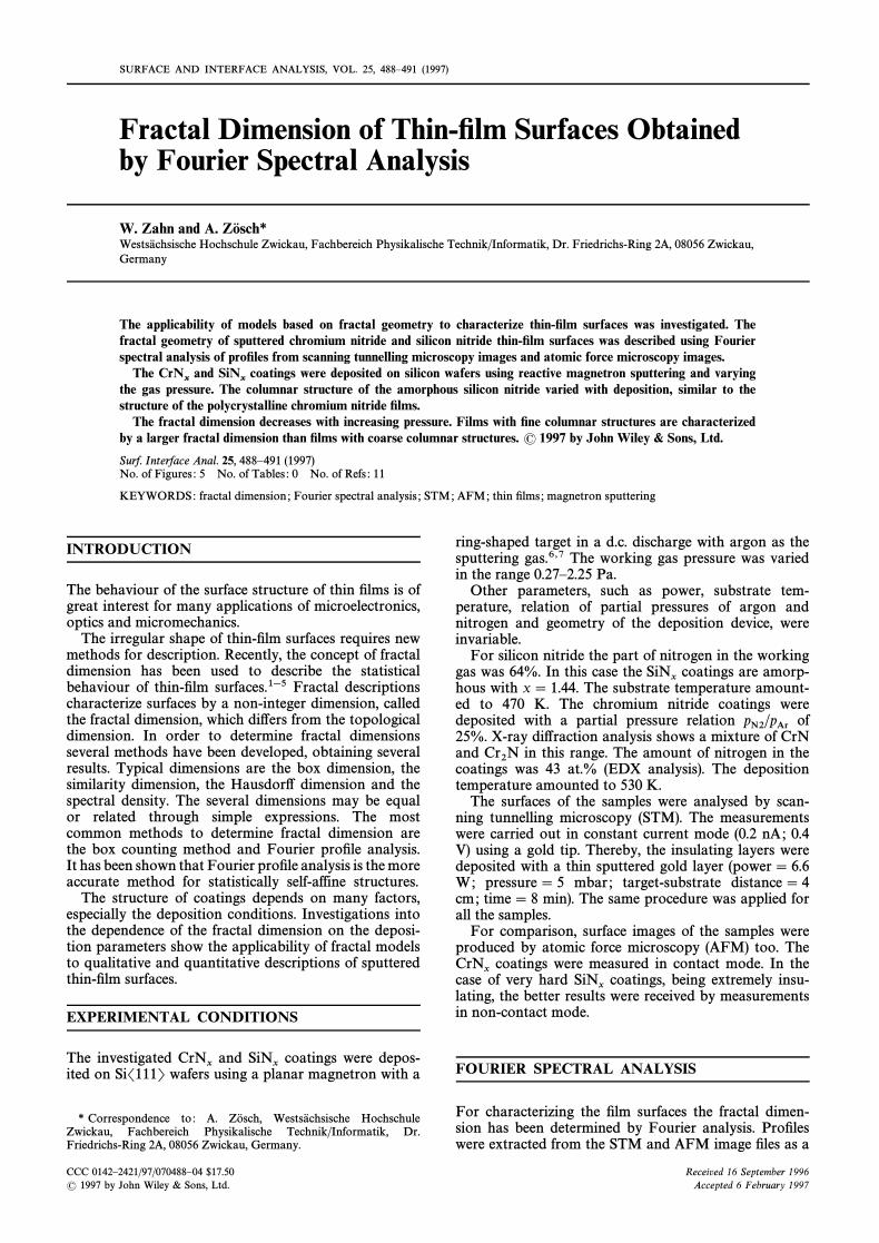
Figure 1. Fourier analysis of a chromium nitride surface (pressure ¼0.38 Pa, AFM). The slope b of the linear part of the averaged powerspectrum and the averaged integrated power spectrum have been determined. The fractal dimension was calculated by D
f¼2.0 ½b/2.
cut through the Ðlm surfaces (linescan) and transformedby a standard Fourier transformation routine. Then thepower spectra were calculated as the square root of thesum of the squared amplitudes of the Fourier coeffi-cients, averaged over ten proÐles and integrated fromhigh to low frequencies. The slope of the linear region ofthe power spectra was determined by linear regression.It has been shown that the slope of the linear region ofthe power spectrum is related to the fractal dimensionof the proÐle through the relation whereDf \ 2.0] b/2,b is the slope of the linear region of the integratedpower spectrum (Fig. 1).3,9h11
RESULTS AND DISCUSSION
The amorphous coatings have a columnar struc-SiNxture similar to polycrystalline coatings. TheCrN
xaverage column diameter of the coatings depositedSiNxat gas pressures of 0.27È2.00 Pa was found in the range
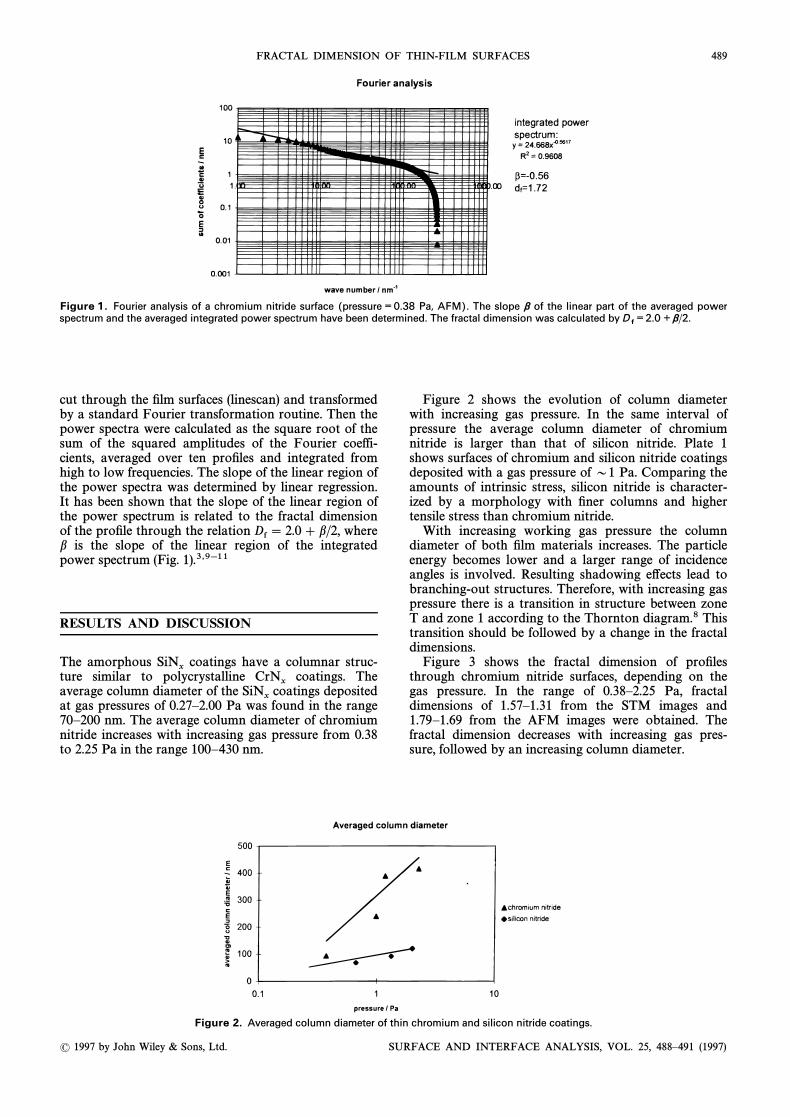
70È200 nm. The average column diameter of chromiumnitride increases with increasing gas pressure from 0.38to 2.25 Pa in the range 100È430 nm.
Figure 2 shows the evolution of column diameterwith increasing gas pressure. In the same interval ofpressure the average column diameter of chromiumnitride is larger than that of silicon nitride. Plate 1shows surfaces of chromium and silicon nitride coatingsdeposited with a gas pressure of D1 Pa. Comparing theamounts of intrinsic stress, silicon nitride is character-ized by a morphology with Ðner columns and highertensile stress than chromium nitride.
With increasing working gas pressure the columndiameter of both Ðlm materials increases. The particleenergy becomes lower and a larger range of incidenceangles is involved. Resulting shadowing e†ects lead tobranching-out structures. Therefore, with increasing gaspressure there is a transition in structure between zoneT and zone 1 according to the Thornton diagram.8 Thistransition should be followed by a change in the fractaldimensions.
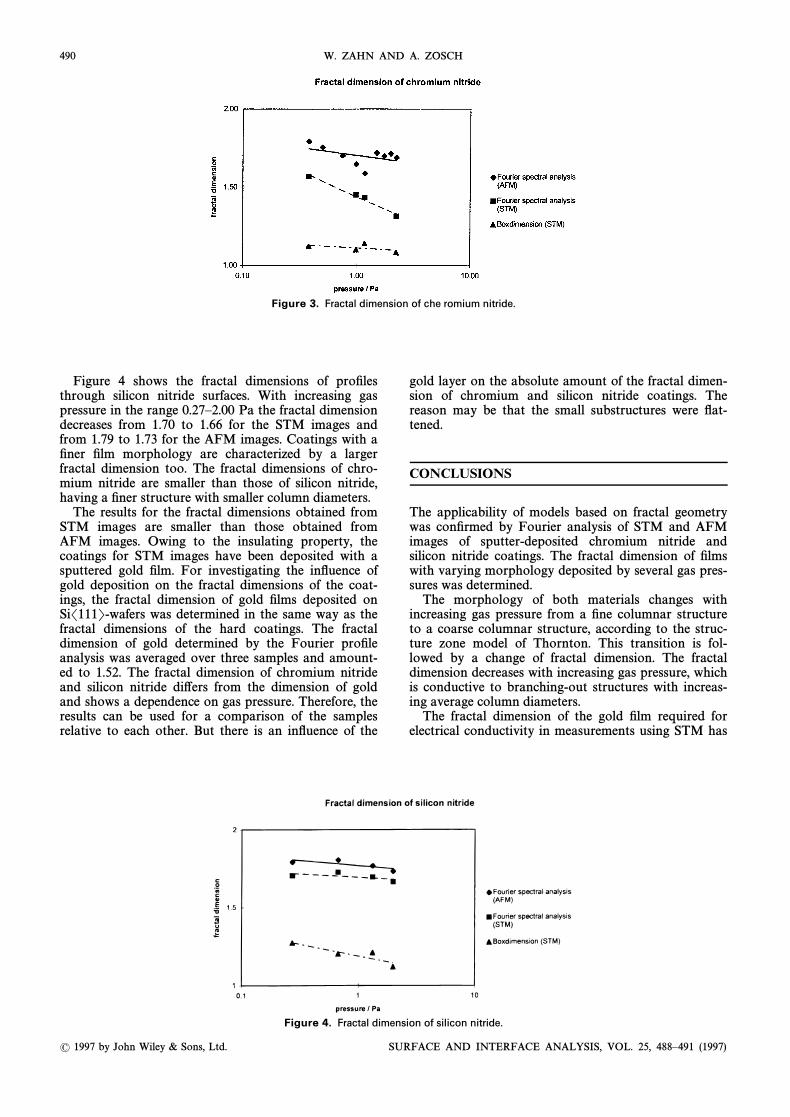
Figure 3 shows the fractal dimension of proÐlesthrough chromium nitride surfaces, depending on thegas pressure. In the range of 0.38È2.25 Pa, fractaldimensions of 1.57È1.31 from the STM images and1.79È1.69 from the AFM images were obtained. Thefractal dimension decreases with increasing gas pres-sure, followed by an increasing column diameter.
Figure 2. Averaged column diameter of thin chromium and silicon nitride coatings.
( 1997 by John Wiley & Sons, Ltd. SURFACE AND INTERFACE ANALYSIS, VOL. 25, 488È491 (1997)
490 W. ZAHN AND A. ZO� SCH
Figure 3. Fractal dimension of che romium nitride.
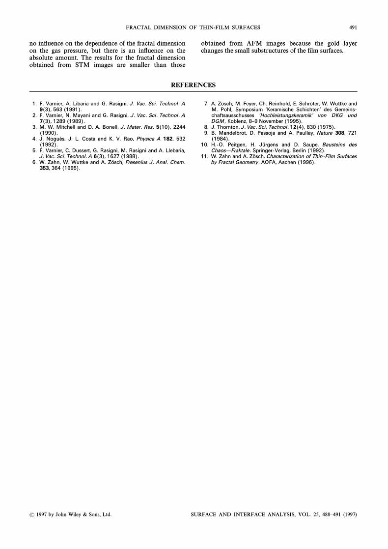
Figure 4 shows the fractal dimensions of proÐlesthrough silicon nitride surfaces. With increasing gaspressure in the range 0.27È2.00 Pa the fractal dimensiondecreases from 1.70 to 1.66 for the STM images andfrom 1.79 to 1.73 for the AFM images. Coatings with aÐner Ðlm morphology are characterized by a largerfractal dimension too. The fractal dimensions of chro-mium nitride are smaller than those of silicon nitride,having a Ðner structure with smaller column diameters.
The results for the fractal dimensions obtained fromSTM images are smaller than those obtained fromAFM images. Owing to the insulating property, thecoatings for STM images have been deposited with asputtered gold Ðlm. For investigating the inÑuence ofgold deposition on the fractal dimensions of the coat-ings, the fractal dimension of gold Ðlms deposited onSiS111T-wafers was determined in the same way as thefractal dimensions of the hard coatings. The fractaldimension of gold determined by the Fourier proÐleanalysis was averaged over three samples and amount-ed to 1.52. The fractal dimension of chromium nitrideand silicon nitride di†ers from the dimension of goldand shows a dependence on gas pressure. Therefore, theresults can be used for a comparison of the samplesrelative to each other. But there is an inÑuence of the
gold layer on the absolute amount of the fractal dimen-sion of chromium and silicon nitride coatings. Thereason may be that the small substructures were Ñat-tened.
CONCLUSIONS
The applicability of models based on fractal geometrywas conÐrmed by Fourier analysis of STM and AFMimages of sputter-deposited chromium nitride andsilicon nitride coatings. The fractal dimension of Ðlmswith varying morphology deposited by several gas pres-sures was determined.
The morphology of both materials changes withincreasing gas pressure from a Ðne columnar structureto a coarse columnar structure, according to the struc-ture zone model of Thornton. This transition is fol-lowed by a change of fractal dimension. The fractaldimension decreases with increasing gas pressure, whichis conductive to branching-out structures with increas-ing average column diameters.
The fractal dimension of the gold Ðlm required forelectrical conductivity in measurements using STM has
Figure 4. Fractal dimension of silicon nitride.
( 1997 by John Wiley & Sons, Ltd. SURFACE AND INTERFACE ANALYSIS, VOL. 25, 488È491 (1997)
FRACTAL DIMENSION OF THIN-FILM SURFACES 491
no inÑuence on the dependence of the fractal dimensionon the gas pressure, but there is an inÑuence on theabsolute amount. The results for the fractal dimensionobtained from STM images are smaller than those
obtained from AFM images because the gold layerchanges the small substructures of the Ðlm surfaces.
REFERENCES
1. F. Varnier, A. Libaria and G. Rasigni, J . Vac. Sci . Technol . A9(3), 563 (1991).
2. F. Varnier, N. Mayani and G. Rasigni, J . Vac. Sci . Technol . A7(3), 1289 (1989).
3. M. W. Mitchell and D. A. Bonell, J . Mater . Res. 5(10), 2244(1990).
4. J. Nogue� s, J. L. Costa and K. V. Rao, Physica A 182, 532(1992).
5. F. Varnier, C. Dussert, G. Rasigni, M. Rasigni and A. Llebaria,J . Vac. Sci . Technol . A 6(3), 1627 (1988).
6. W. Zahn, W. Wuttke and A. Zo� sch, Fresenius J. Anal . Chem.353, 364 (1995).
7. A. Zo� sch, M. Feyer, Ch. Reinhold, E. Schro� ter, W. Wuttke andM. Pohl, Symposium ‘Keramische Schichten’ des Gemeins-chaftsausschusses ‘Hochleistungskeramik’ von DKG undDGM, Koblenz, 8–9 November (1995).
8. J. Thornton, J. Vac. Sci . Technol . 12(4), 830 (1975).9. B. Mandelbrot, D. Passoja and A. Paullay, Nature 308, 721
(1984).10. H.-O. Peitgen, H. Ju� rgens and D. Saupe, Bausteine des
Chaos—Fraktale . Springer-Verlag, Berlin (1992).11. W. Zahn and A. Zo� sch, Characterization of Thin-Film Surfaces
by Fractal Geometry . AOFA, Aachen (1996).
( 1997 by John Wiley & Sons, Ltd. SURFACE AND INTERFACE ANALYSIS, VOL. 25, 488È491 (1997)