Embed Size (px)
Citation preview

Neue Möglichkeiten in Maxwell zur Simulation von LeistungselektronikNew possibilities in Maxwell for the simulation of power electronics
CADFEM Elektromagnetik Technologietage 2021
Leistungselektronik
18. Juni 2021
Rene Fuger, CADFEM (Austria) GmbH

© CADFEM 2021
• With decreasing size and increasing power
hardware design gets more difficult.
• Understanding and determining local behavior is
becoming increasingly important.
• Local loss distributions on the PCB becomes
more significant.
Challenges for Power Electronics Applications
High power
Increased
switching
frequencies
High
efficiency
Steep
switching
edges
Thermal
management
Compact
layout
Eddy effects in
devices
3D Physics
Effects!
3D Physics
Effects!
CADFEM Elektromagnetik Technologietage 2021, Leistungselektronik, 18. Juni 2021 2

© CADFEM 2021
• Efficient calculation of solid losses in a half bridge circuit
• Local loss distribution
• Using harmonic solver to calculate the frequency dependent loss contributions
• Using transient solver to calculate the local time dependent loss distribution
• Local current distribution in busbars
• Unbalanced loads for capacitors
• First resonance of an inductor
• Eddy current analysis to determine the inductance
• AC conduction analysis to determine the capacity
Agenda
CADFEM Elektromagnetik Technologietage 2021, Leistungselektronik, 18. Juni 2021 3

Local Loss Distribution
4

© CADFEM 2021
Switching losses in semiconductor
• Frequency content very high according to
Nyquist criterium (>> fPWM)
• The switching time is significant
Switching vs Ohmic Losses
CADFEM Elektromagnetik Technologietage 2021, Leistungselektronik, 18. Juni 2021 5

© CADFEM 2021
Switching losses in semiconductor
• Frequency content very high according to
Nyquist criterium (>> fPWM)
• The switching time is significant
Switching vs Ohmic Losses
CADFEM Elektromagnetik Technologietage 2021, Leistungselektronik, 18. Juni 2021 6
Ohmic losses in copper
• Losses at phase frequency and harmonics
of PWM frequency (fPWM)
• Eddy effects significant at fPWM

© CADFEM 2021
Switching losses in semiconductor
• Frequency content very high according to
Nyquist criterium (>> fPWM)
• The switching time is significant
Switching vs Ohmic Losses
CADFEM Elektromagnetik Technologietage 2021, Leistungselektronik, 18. Juni 2021 7
Ohmic losses in copper
• Losses at phase frequency and harmonics
of PWM frequency (fPWM)
• Eddy effects significant at fPWM
For many designs
comparable in magnitude!
© CADFEM 2021
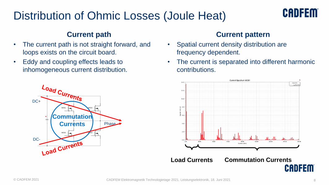
Distribution of Ohmic Losses (Joule Heat)
Current path
• The current path is not straight forward, and
loops exists on the circuit board.
• Eddy and coupling effects leads to
inhomogeneous current distribution.
Current pattern
• Spatial current density distribution are
frequency dependent.
• The current is separated into different harmonic
contributions.
CADFEM Elektromagnetik Technologietage 2021, Leistungselektronik, 18. Juni 2021 8
MOS1 MOS2
MOS3 MOS4
DC+
DC-
Phase
Commutation
Currents
Load Currents Commutation Currents

Using Harmonic Solver to Calculate
the Frequency dependent Loss
Contributions
10

© CADFEM 2021
Currents in Phase Net of First Half Bridge
CADFEM Elektromagnetik Technologietage 2021, Leistungselektronik, 18. Juni 2021 11
Contribution from base signal
(Sine Wave)
Contribution from commutation
currents
(higher spectral content due to modulation
effects and rectangular signals)
Mag (AM_HS_MOS.I)
Mag (AM_LS_MOS.I)
Mag (AM_Phase.I)
Sine (500Hz) PWM Frequency (120kHz)

© CADFEM 2021
Reduction to two Loss Distributions
CADFEM Elektromagnetik Technologietage 2021, Leistungselektronik, 18. Juni 2021 12
Pointwise Split of Losses into Spectral
Contributions
• We are assuming a periodic mode of operation.
• PWM and sinusoidal load frequency are
commensurable.
• Local ohmic loss distribution is given in terms of
the electric field and the current density.
• Decompose time averaged loss distribution into
frequency contributions
Fourier–
Orthonormal
function system
(in time)
© CADFEM 2021
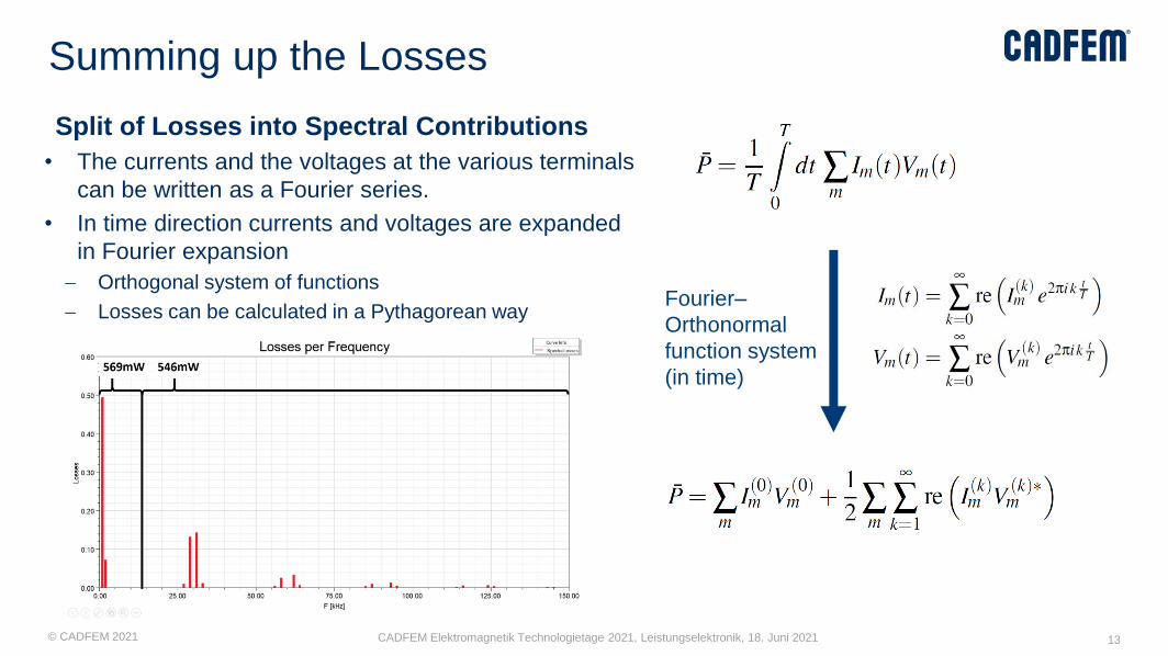
Summing up the Losses
CADFEM Elektromagnetik Technologietage 2021, Leistungselektronik, 18. Juni 2021 13
Split of Losses into Spectral Contributions
• The currents and the voltages at the various terminals
can be written as a Fourier series.
• In time direction currents and voltages are expanded
in Fourier expansion
− Orthogonal system of functions
− Losses can be calculated in a Pythagorean wayFourier–
Orthonormal
function system
(in time)
© CADFEM 2021
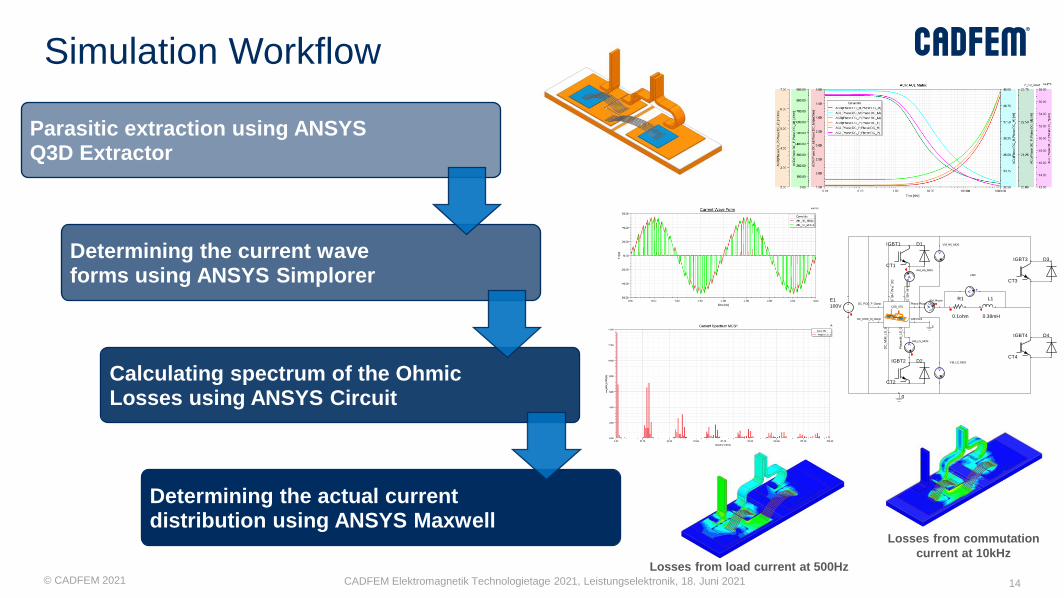
Simulation Workflow
CADFEM Elektromagnetik Technologietage 2021, Leistungselektronik, 18. Juni 2021 14
Parasitic extraction using ANSYS Q3D Extractor
Determining the current wave forms using ANSYS Simplorer
Calculating spectrum of the Ohmic Losses using ANSYS Circuit
Determining the actual current distribution using ANSYS Maxwell
Losses from load current at 500Hz
Losses from commutation
current at 10kHz
0
0
DC
_M
:M_LS
_S
DC
_P
:M_H
S_S
Phase
:M_H
S_D
Phase
:M_LS
_D
DC_M:DC_M_Clamp
DC_P:DC_P_Clamp
GND:Sink
Phase:Phase_ClampQ3D_SS1
R1
0.1ohm
L1
0.38mH
E1
100V
D1
D2
D3
D4
IGBT1
CT1
IGBT2
CT2
IGBT3
CT3
IGBT4
CT4
FML1
Iwish:=Imax*sin(2*pi*Frq*Time)I_band_high:=Iwish+ItolI_band_low:=Iwish-Itol
STATE_11_1
SET: CT1:=1SET: CT2:=0SET: CT3:=0
A
AM_HS_MOS
AAM_LS_MOS
A
AM_Phase
+
V
VM_LS_MOS
+
V
VM_HS_MOS
+V
VM3

© CADFEM 2021
Average Losses Distribution
CADFEM Elektromagnetik Technologietage 2021, Leistungselektronik, 18. Juni 2021 15
Losses from load
current at 500HzLosses from commutation
current at 10kHz
Addition of the loss
contributions for the thermal
simulation

Using Transient Solver to Calculate
the Local Time Dependent Loss
Distribution
CADFEM Elektromagnetik Technologietage 2021, Leistungselektronik, 18. Juni 2021 16

© CADFEM 2021
A new transient solver in Ansys Maxwell based on A-Φ Formulation (magnetic
vector potential A and electric scalar potential Φ)
A (semi)full wave solver including displacement (capacitive) and eddy (inductive)
effects
Maxwell Transient A-Φ Solver
Features
• Partial inductance calculation
• Capacitance Matrix
• J and E fields calculated directly
• Displacement effect
• Multi-terminal conductors support
• …
Applications
• Inverter
• Bus bars
• Electronic transformer
• High voltage/electric field devices
• …
Voltage Conductor
Current & B-Field
CADFEM Elektromagnetik Technologietage 2021, Leistungselektronik, 18. Juni 2021 17
© CADFEM 2021
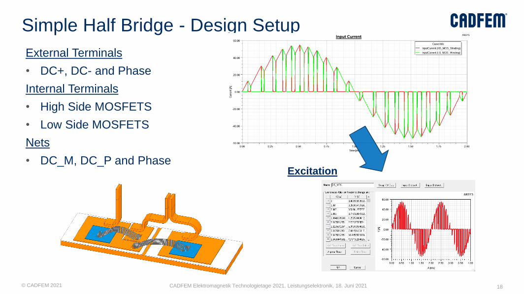
External Terminals
• DC+, DC- and Phase
Internal Terminals
• High Side MOSFETS
• Low Side MOSFETS
Nets
• DC_M, DC_P and Phase
Simple Half Bridge - Design Setup
CADFEM Elektromagnetik Technologietage 2021, Leistungselektronik, 18. Juni 2021 18
Excitation

© CADFEM 2021
Simple Half Bridge - Phase Current & Ohmic Loss
CADFEM Elektromagnetik Technologietage 2021, Leistungselektronik, 18. Juni 2021 19
• Transient behaviour
• Current
• Voltage
• Losses

© CADFEM 2021
Simple Half Bridge - Local Losses
CADFEM Elektromagnetik Technologietage 2021, Leistungselektronik, 18. Juni 2021 20
1.5 ms1.452 ms 1.556 ms
© CADFEM 2021
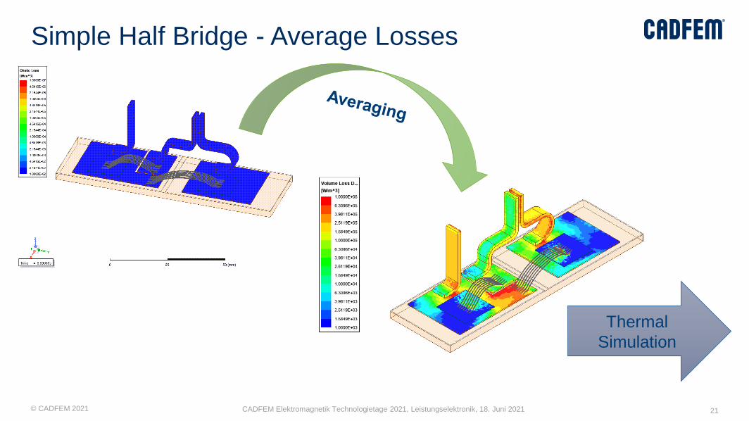
Simple Half Bridge - Average Losses
CADFEM Elektromagnetik Technologietage 2021, Leistungselektronik, 18. Juni 2021 21
Thermal
Simulation

© CADFEM 2021
External Terminals
• DC+, DC- and Phase
Internal Terminals
• Two parallel high side MOSFETS
• Two parallel low side MOSFETS
• Two DC-link capacitor
Nets
• DC_M, DC_P and Phase
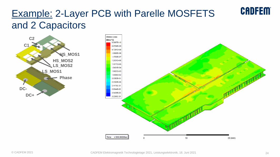
Example: 2-Layer PCB with Parelle MOSFETS
and 2 Capacitors
CADFEM Elektromagnetik Technologietage 2021, Leistungselektronik, 18. Juni 2021 22
DC+
DC-
LS_MOS1
LS_MOS2
HS_MOS1
HS_MOS2
Phase
C1
C2

© CADFEM 2021
Example: 2-Layer PCB with Parelle MOSFETS
and 2 Capacitors
CADFEM Elektromagnetik Technologietage 2021, Leistungselektronik, 18. Juni 2021 23
DC+
DC-
LS_MOS1
LS_MOS2
HS_MOS1
HS_MOS2
Phase
C1
C2
© CADFEM 2021
Example: 2-Layer PCB with Parelle MOSFETS
and 2 Capacitors
CADFEM Elektromagnetik Technologietage 2021, Leistungselektronik, 18. Juni 2021 24
DC+
DC-
LS_MOS1
LS_MOS2
HS_MOS1
HS_MOS2
Phase
C1
C2

Local current distribution in
busbars
CADFEM Elektromagnetik Technologietage 2021, Leistungselektronik, 18. Juni 2021 25
© CADFEM 2021
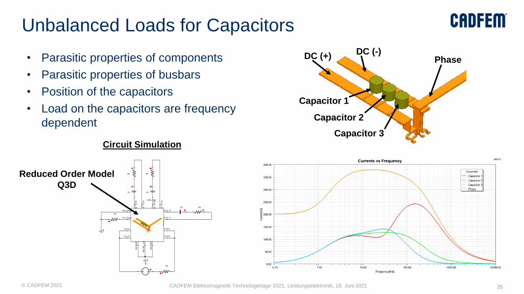
• Parasitic properties of components
• Parasitic properties of busbars
• Position of the capacitors
• Load on the capacitors are frequency
dependent
Unbalanced Loads for Capacitors
CADFEM Elektromagnetik Technologietage 2021, Leistungselektronik, 18. Juni 2021 26
0
0
AC
:AC
1
AC
:AC
2
N:C
1_
N
N:C
2_
N
N:C3_N
N:LS1
N:LS2
P:C
1_
P
P:C
2_
P
P:C3_P
P:HS1
P:HS2
AC
:AC
_L
oa
d
N:N_Supp
P:P_Supp
Q3D_SS1
C1 C2
C3
R2
R3 R4
R5
E1R6
DC (+) PhaseDC (-)
Capacitor 1
Capacitor 2
Capacitor 3
Reduced Order Model
Q3D
Circuit Simulation

© CADFEM 2021
Current Distribution on the Terminals
CADFEM Elektromagnetik Technologietage 2021, Leistungselektronik, 18. Juni 2021 27
• Identifying the input currents for the
different terminals.
• Due to parasitic properties of the
components and busbars the current
can be very different depending on the
frequency.

© CADFEM 2021
Current Distribution on the Terminals
CADFEM Elektromagnetik Technologietage 2021, Leistungselektronik, 18. Juni 2021 28
• Identifying the input currents for the
different terminals.
• Due to parasitic properties of the
components and busbars the current
can be very different depending on the
frequency.

© CADFEM 2021
• Identifying the input currents for the
different terminals.
• Due to parasitic properties of the
components and busbars the current
can be very different depending on the
frequency.
Current Distribution on the Terminals
CADFEM Elektromagnetik Technologietage 2021, Leistungselektronik, 18. Juni 2021 29

© CADFEM 2021
• Local losses indicates possible
hotspots.
• Circulating currents increase losses
near the capacitors.
Ohmic Losses
CADFEM Elektromagnetik Technologietage 2021, Leistungselektronik, 18. Juni 2021 30

First resonance of an inductor
CADFEM Elektromagnetik Technologietage 2021, Leistungselektronik, 18. Juni 2021 31

© CADFEM 2021
• Electric frequency domain solution
− Mixed voltage and current excitation
− Frequency dependent materials
− GC matrix
− Multi-physics coupling
• Applications:
− PCB board
− Circuit parameters extraction
− High voltage application with lossy materials
− Medical applications such as electrical
impedance tomography
New 3D AC Conduction Solutions (Beta)
© AnsysCADFEM Elektromagnetik Technologietage 2021, Leistungselektronik, 18. Juni 2021 32

© CADFEM 2021
Equivalent circuit diagram
CADFEM Elektromagnetik Technologietage 2021, Leistungselektronik, 18. Juni 2021 33
• The inductance and parasitic capacitance
forms a resonant circuit
• The resistance consist of an DC and AC
component
• The components are frequency dependent
© CADFEM 2021
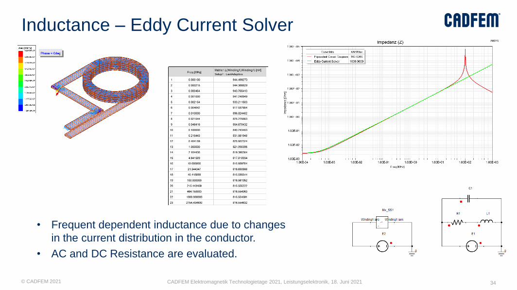
Inductance – Eddy Current Solver
CADFEM Elektromagnetik Technologietage 2021, Leistungselektronik, 18. Juni 2021 34
• Frequent dependent inductance due to changes
in the current distribution in the conductor.
• AC and DC Resistance are evaluated.
© CADFEM 2021
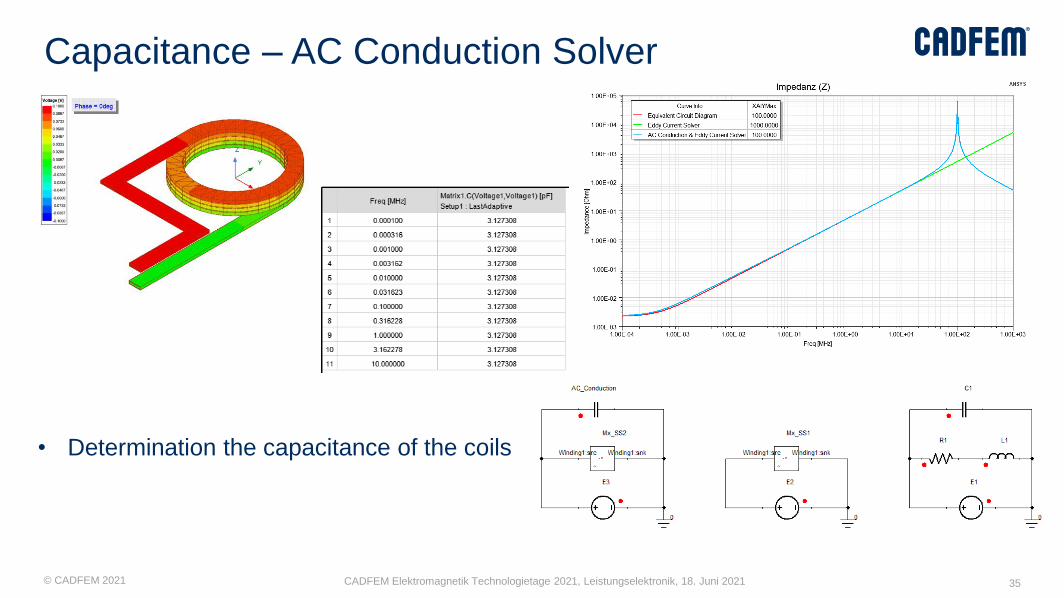
Capacitance – AC Conduction Solver
CADFEM Elektromagnetik Technologietage 2021, Leistungselektronik, 18. Juni 2021 35
• Determination the capacitance of the coils

© CADFEM 2021 37
Summary
• It is important to know the local loss distribution to identify critical regions. Two methods was presented to analyse the local loss distribution.
• The new A-Phi solver allows to calculate the transient behavior and plots the losses for each time step.
• Internal terminals can be used to apply current and voltage wave forms.
• The parasitic probertites of busbars have to be taken into account for circuit simulations to understand the loads on the capacitors.
• Characterization of components regarding parasitic properties be performed with the new AC Conduction solver.

CADFEM
Simulation is more than Software
www.cadfem.net