Embed Size (px)
Citation preview

Luciano Selva Ginani Optical Scanning Sensor System with Submicron Resolution

Berichte aus dem INSTITUT FÜR MASCHINEN- UND GERÄTEKONSTRUKTION (IMGK) Herausgegeben von
Univ.-Prof. Dr.-Ing. Ulf Kletzin (Maschinenelemente), Univ.-Prof. Dr.-Ing. René Theska (Feinwerktechnik) und Univ.-Prof. Dr.-Ing. Christian Weber (Konstruktionstechnik)
aus dem Institut für Maschinen- und Gerätekonstruktion (IMGK) an der TU Ilmenau. Band 24 Diese Reihe setzt die „Berichte aus dem Institut für Maschinenelemente und Konstruktion“ fort.
Optical Scanning Sensor System
with Submicron Resolution
Luciano Selva Ginani
Universitätsverlag Ilmenau 2013

Impressum Bibliografische Information der Deutschen Nationalbibliothek Die Deutsche Nationalbibliothek verzeichnet diese Publikation in der Deutschen Nationalbibliografie; detaillierte bibliografische Angaben sind im Internet über http://dnb.d-nb.de abrufbar.
Diese Arbeit hat der Fakultät für Maschinenbau der Technischen Universität Ilmenau als Dissertation vorgelegen. Tag der Einreichung: 28. Februar 2013 1. Gutachter: Univ.-Prof. Dr.-Ing. René Theska
(Technische Universität Ilmenau) 2. Gutachter: Univ. -Prof. Dr.-Ing. habil. Eberhard Manske
(Technische Universität Ilmenau) 3. Gutachter: Prof. Dr. Herman Lepikson
(Universidade Federal da Bahia) Tag der Verteidigung: 21. Mai 2013
Technische Universität Ilmenau/Universitätsbibliothek Universitätsverlag Ilmenau Postfach 10 05 65 98684 Ilmenau www.tu-ilmenau.de/universitaetsverlag Herstellung und Auslieferung Verlagshaus Monsenstein und Vannerdat OHG Am Hawerkamp 31 48155 Münster www.mv-verlag.de ISSN 2191-8082 (Druckausgabe) ISBN 978-3-86360-068-6 (Druckausgabe) URN urn:nbn:de:gbv:ilm1-2013000337
Geleitwort derHerausgeber
Schriftenreihe des Instituts für Maschinen- und Gerätekonstruktion,Band 24:
Luciano Selva GinaniOptical Scanning Sensor System with Submicron Resolution
Die Konstruktion von Maschinen und Geräten sowie die zugehöri-gen Methoden und Werkzeuge sind seit den frühen 1950er Jahren einprofilbildender Schwerpunkt an der Technischen Universität Ilmenauund ihren Vorgängerinstitutionen. Es war daher ein nahe liegenderSchritt, dass die drei konstruktiv orientierten Fachgebiete der Fakultätfür Maschinenbau - Maschinenelemente, Feinwerktechnik/PrecisionEngineering, Konstruktionstechnik - im Mai 2008 das Institut für Ma-schinen- und Gerätekonstruktion (IMGK) neu gegründet haben. DasIMGK steht in der Tradition einer Kette ähnlicher Vorgängerinstitute,deren wechselnde Zusammensetzung hauptsächlich durch sich überder Zeit ändernde Universitätsstrukturen bedingt war.
Zweck des Institutes ist es, die Kompetenzen und Ressourcen der be-teiligten Fachgebiete zu bündeln, um Forschung und Lehre zu ver-bessern und erzielte wissenschaftliche Ergebnisse gemeinsam in dieFachöffentlichkeit zu tragen.
Ein wesentliches Instrument hierzu ist die Schriftenreihe des Institutsfür Maschinen- und Gerätekonstruktion. Sie führt eine erfolgreicheSchriftenreihe des im Jahr 1991 gegründeten unmittelbaren Vorgän-gerinstitutes IMK (Institut für Maschinenelemente und Konstruktion)fort.

vi
In der Schriftenreihe erscheinen in erster Linie die am Institut entstan-denen Dissertationen, daneben werden aber auch andere Forschungs-berichte, die in den thematischen Rahmen passen und von allgemei-nem Interesse sind, in die Schriftenreihe aufgenommen.
Der vorliegende Band 24 ist als Dissertation am Fachgebiet Feinwerk-technik entstanden.
Die Herausgeber wünschen sich reges Interesse an der Schriftenreiheund würden sich freuen, wenn sie zum fruchtbaren Dialog in Wissen-schaft und Praxis beitragen würde.
Ilmenau, im März 2013
Univ.-Prof. Dr.-Ing. Ulf Kletzin (Maschinenelemente)Univ.-Prof. Dr.-Ing. René Theska (Feinwerktechnik)
Univ.-Prof. Dr.-Ing. Christian Weber (Konstruktionstechnik)
Abstract
Laser Scanning Microscopy (LSM) has been used for a long time in thefield of surface measurement and is today one of the most promisingtechnologies for fast, accurate and repeatable measurements in appli-cation areas such as material science, microelectronics, medical tech-nology, and, especially, nanotechnology. Its basic concept was origi-nally developed in 1957 by Marvin Minsky, and it is basically a tech-nique for increasing contrast and resolution in optical imaging sys-tems through the rejection of out-of-focus light. Images are acquiredpoint-by-point and reconstructed with a computer, allowing the three-dimensional reconstruction of complex objects.
All modern laser scanning microscope designs are centred on conven-tional upright or inverted optical microscope arrangements and theuse of standard high-end objectives lenses with high numerical aper-ture, for which there is a large design experience basis. In this work,autofocus and optical scanning technologies are brought together inthe design and construction of an alternative simplified scanning mi-croscope for surface measurements in millimetre range with sub-mi-crometer resolution. The developed system uses an autofocus sensorbased on the Foucault knife-edge principle to generate a defocus sig-nal and a high precision piezo positioning stage for translating the ob-jective and scanning the samples in the axial direction. For the lateralscanning, a piezo driven tip-tilt mirror is used.
The developed scanning microscope is built with a reduced number ofoptical components and designed to offer a simple and versatile exper-imental set-up for the measurement and analysis of errors induced byoptical aberrations due to the use of suboptimal optics in scanning mi-croscopy. The reduction of the number of optical components and theuse of simple uncompensated lenses has always been avoided in scan-ning microscopy as it inserts optical aberrations into the system, gen-erating asymmetries in the defocus signal and deteriorating its overall
viii
performance. The traditional way of solving this problem is to im-prove the optical system such that it works as a paraxial lens, but thatcomes with the price of heavy and costly optics. Thanks to advancesmade in modern computing power, it is now possible to consider un-conventional alternatives to optics optimization.
By breaking the paradigm of improving the optics to a paraxial lensand observing the optics as part of a complex system, it is possibleto use simpler optics and correct the resultant errors computationally.These errors are systematic and, as long as they can be measured andmodelled, can be predicted and corrected. This way, the design of theoptical system becomes much more flexible and the task of error han-dling can be divided between optics optimization and computationalcorrection, reducing overall size and weight, raising system dynam-ics and reducing costs, without losing accuracy. The goal is not tostudy each optical aberration individually, but to measure and modeltheir combined influence in the measurements. Different strategies foraddressing these measurement errors caused by the use of uncompen-sated optics are proposed, discussed and experimentally validated.
Zusammenfassung
Laser-Scanning Mikroskopie (LSM) ist eine seit langer Zeit im Bereichder Oberflächenmessung sehr wichtige und sehr vielversprechendeTechnologie für schnelle, genaue und wiederholbare Messungen inAnwendungsbereichen wie Mikroelektronik, Medizintechnik, Mate-rialwissenschaft und insbesondere Nanotechnologie. Das Grundprin-zip wurde ursprünglich im Jahre 1957 von Marvin Minsky entwickelt.Es ist im Grunde eine Technik zur Erhöhung von Kontrast und Auflö-sung in optischen Abbildungssystemen. Ein Prüfling wird punktwei-se abgetastet und ein Bild seiner Oberfläche mit Hilfe eines Rechnerserfasst und rekonstruiert, sodass die Aufnahme von komplexen drei-dimensionalen Objekten möglicht ist.
Alle modernen Scanning Mikroskope basieren auf der herkömmlichenaufrechten oder umgekehrten Bauweise von Lichtmikroskopen un-ter Verwendung von High-End Mikroskopobjektiven mit hoher nu-merischer Apertur. In dieser Arbeit werden Autofokus- und optischeAbtastverfahren in der Entwicklung und Konstruktion eines alternati-ven, vereinfachten Scanning Mikroskops für Oberflächenmesstechnikim Millimeterbereich mit Sub-Mikrometer Auflösung zusammenge-bracht. Das System verwendet einen auf dem Foucault’sches Schnei-denverfahren basierenden Autofokussensor um die Fokuslage zu be-stimmen und einen hochpräzisen Piezo-Linearantrieb für die Verschie-bung des Objektivs entlang der optischen Achse sowie das Abtastendes Prüflings in der axialen Richtung. Die laterale Abtastung des Prüf-lings wird durch den Einsatz eines Piezo-Spiegels realisiert, der umzwei Achsen schwenkbar ist.
Das entwickelte Scanning Mikroskop hat eine reduzierte Anzahl vonoptischen Komponenten und bietet einen einfachen und vielseitigenVersuchsaufbau zur Messung und Analyse von Fehlern, die durchdie bewusste Verwendung von unkompensierten Optiken und derenentsprechende Abbildungsfehler auftreten. Die Verringerung der An-

x
zahl der optischen Komponenten und der Einsatz einfacher, unkom-pensierter Linsen wird prinzipiell in der Scanning-Mikroskopie ver-mieden. Die damit verbundenen Abbildungsfehler erzeugen Asym-metrien in den Autofokussensoren und beeinträchtigen die Gesamt-leistung. Die herkömmliche Lösung dieser Problematik ist das Systemdurch Addition zusätzlicher optischer Komponenten zu verbessern,sodass es wie ein paraxiales System für den gesamten Funktionsbe-reich wirkt. Diese Verbesserung bringt aber die Nachteile von Baugrö-ße, Gewicht und Kosten mit sich. Unter Berücksichtigung der heuti-gen verfügbaren Rechenleistung, ist es jetzt möglich, unkonventionel-le Alternativen zur Optimierung der Optik in Betracht zu ziehen.
Durch das Brechen des Paradigmas der Verbesserung der Optik bis zueinem paraxialen System und die Betrachtung der Optik als Teil eineskomplexen Systems ist es möglich, simplere Optik zu verwenden, unddie resultierenden Fehler rechnerisch zu korrigieren. Diese Fehler sindsystematisch und können - solange sie modelliert und gemessen wer-den können - vorhergesagt und korrigiert werden. Damit wird dasDesign des optischen Systems wesentlich flexibler und die Aufgabeder Fehlerbehandlung zwischen Optimierung der Optik und rechne-rischer Korrektur aufgeteilt. Baugröße, Gewicht und Kosten könnendann reduziert werden und die Systemdynamik erhöht sich, ohne Ein-schränkung der Präzision. Das Ziel ist nicht jeden Abbildungsfehlerindividuell zu untersuchen, sondern deren Zusammenwirken auf dieMessungen zu beobachten und zu modellieren. Verschiedene Strate-gien für die Behandlung dieser Messfehler werden in dieser Arbeitvorgeschlagen, diskutiert und experimentell validiert.
Vorwort
Die vorliegende Dissertation entstand während meiner Tätigkeit alswissenschaftlicher Mitarbeiter am Fachgebiet Feinwerktechnik in derTechnischen Universität Ilmenau. Diese Arbeit wurde mit Mitteln derDeutsche Forschungsgemeinschaft (DFG) im Rahmen des Sonderfor-schungsbereich SFB622 “Nanopositionier- und Nanomessmaschinen”und der Johannes Hübner Stiftung Gießen (JHS) unter dem Projekt Nr.01/10 “Entwicklung optisch scannender Sensorsysteme” gefördert.
An erster Stelle möchte ich meinem Doktorvater Herrn Prof. Dr.-Ing.René Theska, Direktor des Instituts für Maschinen- und Gerätekon-struktion und Inhaber des Lehrstuhls für Feinwerktechnik an der Tech-nischen Universität Ilmenau, herzlich danken. Er hat immer an meinPotenzial geglaubt und durch seine persönliche Unterstützung undsein Vertrauen diese Arbeit ermöglicht. Seine wissenschaftliche Be-treuung und wertvollen Anregungen haben mich immer vorangetrie-ben.
Herrn Prof. Dr.-Ing Eberhard Manske, Leiter des Fachgebietes Präzi-sionsmesstechnik an der Technischen Universität Ilmenau, und HerrnProf. Dr. Herman Augusto Lepikson, an der Bundesuniversität vonBahia (Brasilien), danke ich für die Übernahme der Gutachten der Ar-beit und die wertvollen Hinweise zu meiner Dissertationsschrift.
Meinen Kollegen Kerstin John, Tobias Hackel und Christoph Hahmsowie allen Mitarbeitern der Fachgebiet Feinwerktechnik und des Gra-duiertenkollegs des SFB622 danke ich für die Zusammenarbeit unddie zahlreichen wissenschaftlichen Gesprächen und Diskussionen, diemir stets neue Ideen und Anregungen boten.
Ich bedanke mich ebenso bei der Johannes Hübner Stiftung für die fi-nanzielle Förderung der Arbeit. Ohne ihre Unterstützung wäre dieseArbeit nicht möglich gewesen. Sie hat durch eine unkomplizierte undunbürokratische Vorgehensweise meine Arbeit und wissenschaftliche

xii
Freiheit immer gefördert und unterstützt. Ihr Vertrauen und ihre Un-terstützung waren essenziell für den Abschluss meiner Promotion.
Ein besonders herzlicher Dank gilt meinen Eltern. Mit ihrer Unterstüt-zung, unendlichen Geduld und freundlichem Nachdruck haben siebeständig meine Bestrebungen zur Erweiterung meines Horizonts ge-fördert.
Ilmenau, März 2013Luciano Selva Ginani
Contents
Abstract vii
Zusammenfassung ix
Vorwort xi
Abbreviations and Symbols xv
1 Introduction 11.1 Optical Measuring Technologies and Systems . . . . . . 41.2 Objectives and Structure . . . . . . . . . . . . . . . . . . 6
2 Fundamentals and State of the Art 92.1 Principles of Optics . . . . . . . . . . . . . . . . . . . . . 9
2.1.1 The Nature of Light . . . . . . . . . . . . . . . . 92.1.2 Geometric Optics . . . . . . . . . . . . . . . . . . 102.1.3 Ray-Tracing . . . . . . . . . . . . . . . . . . . . . 122.1.4 Optical Aberrations . . . . . . . . . . . . . . . . 17
2.2 Confocal Microscopy . . . . . . . . . . . . . . . . . . . . 202.3 Resolution Limits of Optical Instruments . . . . . . . . 232.4 Auto-focus in Optical Systems . . . . . . . . . . . . . . . 26
2.4.1 Astigmatic Method . . . . . . . . . . . . . . . . . 262.4.2 Foucault Knife-Edge Method . . . . . . . . . . . 32
2.5 Optical Scanning . . . . . . . . . . . . . . . . . . . . . . 362.6 Modern Confocal Laser Scanning Microscopy . . . . . . 38
3 Design and Development of a Simplified Scanning Micro-scope 413.1 Basic Design . . . . . . . . . . . . . . . . . . . . . . . . . 413.2 Telecentricity . . . . . . . . . . . . . . . . . . . . . . . . . 463.3 Scanning Procedure . . . . . . . . . . . . . . . . . . . . . 473.4 Control and Data Acquisition . . . . . . . . . . . . . . . 50
xiv
4 Modelling, Simulation and Calibration 534.1 Correction vs Compensation . . . . . . . . . . . . . . . . 544.2 Error Correction in Scanning Systems . . . . . . . . . . 554.3 Model Based Error Correction . . . . . . . . . . . . . . . 57
4.3.1 Paraxial Model . . . . . . . . . . . . . . . . . . . 594.3.2 Ray-Tracing Model . . . . . . . . . . . . . . . . . 694.3.3 Model Calibration . . . . . . . . . . . . . . . . . 75
4.4 Measurement Based Error Correction . . . . . . . . . . 814.4.1 Look-up Table . . . . . . . . . . . . . . . . . . . . 834.4.2 Polynomials . . . . . . . . . . . . . . . . . . . . . 85
5 Experimental Results 895.1 Characteristic Curve of the Sensor . . . . . . . . . . . . 895.2 Error and Sensitivity Analysis . . . . . . . . . . . . . . . 925.3 Model Calibration and Function Measurement . . . . . 965.4 Error Correction Methods . . . . . . . . . . . . . . . . . 975.5 Influence of the Model Calibration . . . . . . . . . . . . 1035.6 Influence of Sample Inclination in the Measurements . 1045.7 Vertical and Lateral Resolution and Noise . . . . . . . . 107
5.7.1 Vertical Resolution and Noise . . . . . . . . . . . 1085.7.2 Lateral Resolution and Noise . . . . . . . . . . . 110
5.8 Repeatability . . . . . . . . . . . . . . . . . . . . . . . . . 1155.9 Comparison with other Measurement Systems . . . . . 1165.10 Ray-Tracing Implementations . . . . . . . . . . . . . . . 117
6 Measurement Tasks and Applications 121
7 Conclusions and Further Work 1257.1 Conclusions . . . . . . . . . . . . . . . . . . . . . . . . . 1257.2 Further Work . . . . . . . . . . . . . . . . . . . . . . . . 126
List of Figures 132
List of Tables 133
Bibliography 142
Abbreviations andSymbols
Abbreviations
ADC Analog Digital ConverterAFM Atomic Force MicroscopeASP AsphereCCD Charged Coupled DeviceCMM Coordinate Measuring MachineCMOS Complementary Metal-Oxide SemiconductorCPU Central Processing UnitDAC Digital Analog ConverterDSP Digital Signal ProcessingDVD Digital Versatile DiskFES Focus Error SignalFWHM Full Width at Half MaximumGPU Graphic Processing UnitHOE Holographic Optical ElementIEEE Institute of Electrical and Electronics EngineersLMA Levenberg-Marquardt AlgorithmLSM Laser Scanning MicroscopyLUT Lookup TableMEMS Micro-Electro-Mechanical SystemMOEMS Micro-Opto-Electro-Mechanical SystemNA Numerical ApertureNPMM Nanopositioning and Measuring MachinePCX Plan ConvexPI Proportional IntegralPSD Position Sensitive Device

xvi
RMS Root Mean SquareSPM Scanning Probe MicroscopySEM Scanning Electron Microscopy
xvii
Symbols
Symbol Unit Descriptionα rad Field Anglef mm Focal Lengthλ nm Wavelengthn - Refractive Indexδ μm Defocusβ ◦ Sample Inclinationβmax
◦ Maximum Measurable Sample In-clination
θx mrad Mirror Tilting Angleθy mrad Mirror Tilting AngleΔz μm Objective DisplacementVx V Voltage Control Signal for the Mir-
ror Tilting AngleVy V Voltage Control Signal for the Mir-
ror Tilting AngleVz V Voltage Control Signal for the Ob-
jective DisplacementDIF V Difference Voltage SignalSUM V Sum Voltage Signal[Px, Py, Pz] mm Measured Point CoordinatesFLSM - Function of the Laser Scanning Mi-
croscopeJLSM - Jacobian Matrix of the Function
FLSMQ - Parameters of the Function FLSMTi,j - Homogeneous TransformationTx - Translation along the X-axisTy - Translation along the Y-axisTz - Translation along the Z-axisRx - Rotation on the X-axisRy - Rotation on the Y-axisRz - Rotation on the Z-axis�Si - Mathematical Description of an
Optical Surface

xviii
�Ri - Mathematical Description of anOptical Ray
�N - Normal Vector of an Optical Sur-face
C mm−1 Surface CurvatureK - Conic ConstantTH mm Lens ThicknessKi - Aspheric Coefficients

Chapter 1
Introduction
In many ways the nanotechnology era has already began. Nanotech-nology is a very broad and fast developing field. It can be defined as acollection of different techniques and approaches, which take advan-tage of the physical properties of dimensions on the nanometre scaleto the production of structures and devices with novel or optimizedcharacteristics and features. [Hul07, SS02]. Numerous forecasts pre-dicting massive growth in the nanotechnology markets have appearedin recent years and almost daily new nanofabrication technologies andnanodevices based on electrical, optical, magnetic, mechanical, chem-ical and biological effects are reported [Bog07, Hul07, SS02, DDX+10].But so that such technology may indeed start a new revolution, it mustbe underpinned by a reliable metrology infrastructure that is yet notfully available [HCHD06, Hul07, SS02, LBB+10, Gra07].
Metrology is a vital part of industrial manufacturing as it enables net-works of services, suppliers and communications to work with effi-ciency and reliability, but when the dimensions are reduced from themicro to the nanoscale there are major differences in the associatedmetrological requirements [Bog07]. Dimensional metrology for nan-otechnology requires measuring instruments to provide shape andsize information with atomic levels of resolution and precision, andthat has to be done within seconds. This precise and fast measurementof structures from macro to nano in constantly increasing volumes ofup to several hundred millimetres with nanometer precision is a con-stantly increasing demand of today’s industry. Such requirements aremostly evident in fields such as microelectronics, data storage and ad-vanced photonics, where the technological progress is characterized
2
by reductions in size, although precision in the nanoscale is already arequirement for many industrial and research fields. Precision engi-neering, lithography, nanomaterials, thin films, optics, micromechan-ics and many other industries work today on the limits of actual in-strumentation.
This tendency to miniaturisation is growing and spreading to otherfields and, in order to support this expansion and to promote thefurther development of these high-end industries, accessible and re-liable instruments that allow the measurement and manipulation ofstructures with nanometer precision are necessary. This can alreadybe seen in most of the state-of-the-art measuring equipments in useor under development today. Electron Microscopy (EM), ScanningProbe Microscopy (SPM) and near field microscopy are just a few ex-amples [Bog07,SMGH95,DDX+10,WPH06]. Scanning electron micro-scopes (SEM) and atomic force microscopes (AFM) are the most com-monly used instruments.
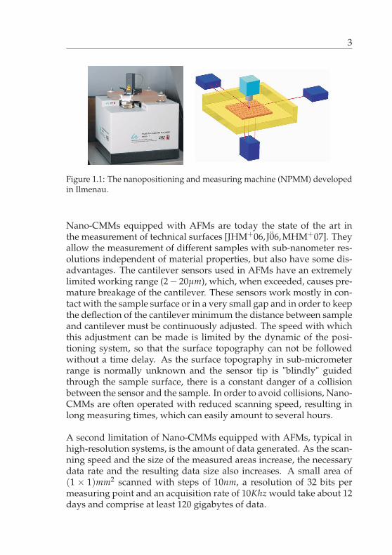
Most of the systems used for the measurement of structures in thenanoscale have a very limited working range and are therefore oftenused as probing systems in coordinate measuring machines (CMMs).In such applications, the obtained precision is determined by the CMMused for positioning the samples and measuring instruments [Bog07].This important role played by CMMs led to the recent developmentof the μ-CMMs and more recently the Nano-CMMs, which are able toachieve resolutions in the sub-nanometric range in working volumesup to a few millimetres [Bog07, SS02, HTB+06, TFHL04, Hac10]. Fig-ure 1.1 shows such a Nano-CMM developed in the Ilmenau Universityof Technology and its basic working principle.
The nanopositioning and nanomeasuring machine (NPMM) uses threeinterferometers arranged in a way to build a cartesian coordinate sys-tem so that their light beams virtually intersect at a single point locatedon the tip of the probing system. This way the distance between thepoint of measurement and the reference line of the measurement sys-tem, and therefore the Abbe-Error, are minimized. The machine has aworking volume of 25mm × 25mm × 5mm, a resolution of 0.01nm anda positioning uncertainty of less than 10nm in all three axes. It alsoallows the use of different probe systems for accomplishing variousmeasuring or machining tasks.
3
Figure 1.1: The nanopositioning and measuring machine (NPMM) developedin Ilmenau.
Nano-CMMs equipped with AFMs are today the state of the art inthe measurement of technical surfaces [JHM+06, J0̈6,MHM+07]. Theyallow the measurement of different samples with sub-nanometer res-olutions independent of material properties, but also have some dis-advantages. The cantilever sensors used in AFMs have an extremelylimited working range (2− 20μm), which, when exceeded, causes pre-mature breakage of the cantilever. These sensors work mostly in con-tact with the sample surface or in a very small gap and in order to keepthe deflection of the cantilever minimum the distance between sampleand cantilever must be continuously adjusted. The speed with whichthis adjustment can be made is limited by the dynamic of the posi-tioning system, so that the surface topography can not be followedwithout a time delay. As the surface topography in sub-micrometerrange is normally unknown and the sensor tip is "blindly" guidedthrough the sample surface, there is a constant danger of a collisionbetween the sensor and the sample. In order to avoid collisions, Nano-CMMs are often operated with reduced scanning speed, resulting inlong measuring times, which can easily amount to several hours.
A second limitation of Nano-CMMs equipped with AFMs, typical inhigh-resolution systems, is the amount of data generated. As the scan-ning speed and the size of the measured areas increase, the necessarydata rate and the resulting data size also increases. A small area of(1 × 1)mm2 scanned with steps of 10nm, a resolution of 32 bits permeasuring point and an acquisition rate of 10Khz would take about 12days and comprise at least 120 gigabytes of data.
4
One way to overcome these problems is the use of feature-orientedmeasurements, where the step size, and therefore the data density, canbe altered during the measurement. This way, simple regions withoutimportant features can be measured with low data density and impor-tant areas with high density, obtaining an increase in the measuringthroughput and a reduction in the overall data size and measurementtime.
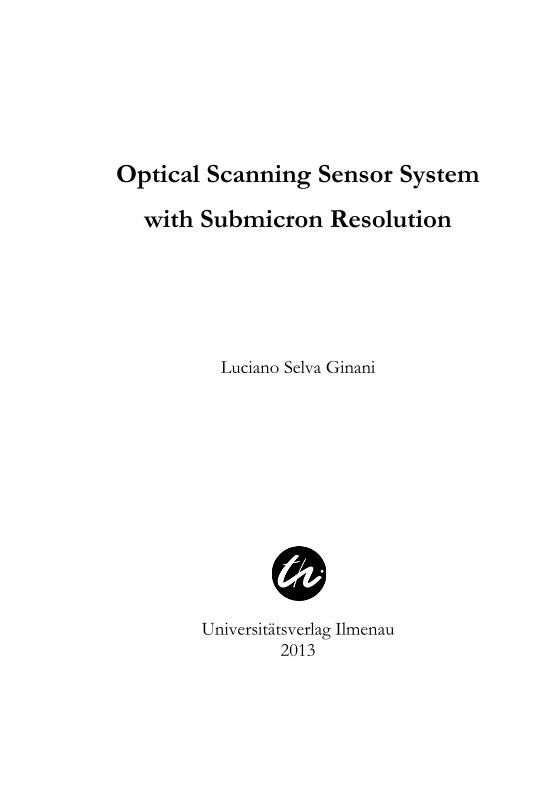
However, that is not possible with the use of a single sensor. For theefficient measurement of extended areas, the integration of multiplesensors is necessary. In this work, an alternative to overcome these dif-ficulties, based on the development of a novel fast miniaturized opti-cal pre-scanning system, is proposed. The pre-scanning system allowsa rapid parallel measurement of the sample topography, so that a pri-ori information about the sample in the sub-micrometer range can beacquired and used to optimize measurement planning and scanningspeeds of the more precise sensor without data or precision losses andwithout risking a collision between sensor and sample.
In this context, non-contact measuring systems and optical scanningplay an important role. Merbach [Mer84] discussed the importance ofthese systems and presented in his work a systematic analysis of dif-ferent non-contact technologies and their use in dimensional measur-ing, while Barthel [Bar85] discussed in more detail the use of opticaltechnologies for non-contact dimensional measuring.
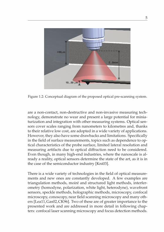
Figure 1.2 illustrates an example of a measuring task using a cantileversensor and the typical dimensions involved. With the use of an opti-cal pre-scanning system, the collision risk between the cantilever andthe step can be detected and the data density of the measurement ad-justed, optimizing the measuring task.
1.1 Optical Measuring Technologies and
Systems
Optical technologies are a key technology in many technical fields andoptical based sensors and systems are today an essential tool in metrol-ogy. They not only offer a flexible, fast and robust measurement, butalso distinguish themselves through a multitude of advantages. They
5
>50�m
10...50 �m
2...8mm
Figure 1.2: Conceptual diagram of the proposed optical pre-scanning system.
are a non-contact, non-destructive and non-invasive measuring tech-nology, demonstrate no wear and present a large potential for minia-turization and integration with other measuring systems. Optical sen-sors cover scales ranging from nanometers to kilometres and, thanksto their relative low cost, are adopted in a wide variety of applications.However, they also have some drawbacks and limitations. Specificallyin the field of surface measurements, topics such as dependence to op-tical characteristics of the probe surface, limited lateral resolution andmeasuring artifacts due to optical diffraction need to be considered.Even though, in many high-end industries, where the nanoscale is al-ready a reality, optical sensors determine the state of the art, as it is inthe case of the semiconductor industry [Kni03].
There is a wide variety of technologies in the field of optical measure-ments and new ones are constantly developed. A few examples aretriangulation methods, moiré and structured light methods, interfer-ometry (homodyne, polarization, white light, heterodyne), wavefrontsensors, speckle methods, holographic methods, microscopy, confocalmicroscopy, conoscopy, near field scanning microscopy and many oth-ers [Lea11,Gas02,CK96]. Two of these are of greater importance to thepresented work and are addressed in more detail in following chap-ters: confocal laser scanning microscopy and focus detection methods.
6
Nevertheless, all these technologies share as a common point the useof optical systems and sensors, combining many different technicalfields and using light as information carrier for measuring differentparameters and properties. While the optical sensor is responsible forconverting light rays into electronic signals, the optical system is re-sponsible for capturing, shaping and directing those rays and is thecore of most optical measurements.
An optical system is a group of lens, mirrors, prisms, and other opti-cal elements, placed in a specific configuration to reflect, refract, dis-perse, absorb, polarize, or otherwise interact with light. These specificconfigurations or schemas are normally chosen so that optical aber-rations are minimized and the optical system may be described withthe paraxial approximation. This is nowadays mostly done with theuse of computer aided optimization techniques in order to improvethe performance of the optical system until the desired tolerances areachieved and, for achieving tight tolerances, the number of necessaryelements is often large, leading to large and heavy optics.
A second point of interest in this work is to consider software basedalternatives to optical optimization. Considering the optics as part of acomplex system, it is possible to use simple non-optimized optics andcorrect a part of their optical errors computationally. By observing theeffects of optical aberrations in the measurement system as a whole,the task of minimizing these errors can be divided between the opti-cal design and the post-processing of the measurement data, so that,with the use of simpler optics, overall weight and size can be reducedas well as costs, facilitating miniaturization and integration of opticalmeasurement systems in different applications.
1.2 Objectives and Structure
The objective of this work is to develop and design a fast optical scan-ning system for technical surfaces based on the use of simple uncom-pensated optics and its validation. The proposed system is designed toreduce overall costs and weight, improving measurement speed andsystem dynamic and expanding the possibilities for miniaturization.In order to overcome the effects of optical aberrations caused by theuse of simple optics, a novel approach is proposed, where the effects of
7
these aberrations in the measurements are computationally corrected.This way, through computation and intelligent measuring, more in-formation can be extracted from the system and the control of opticalaberrations can be divided between optical compensation (hardware)and data correction (software), offering more flexibility for the system’sdesign.
This work was developed within the framework of the CollaborativeResearch Centre 622: Nanopositioning and Measuring Machines from theDeutsche Forschungsgemeinschaft (DFG) and was also supported by theJohannes Hübner Stiftung. It is structured in seven chapters emphasiz-ing the following points:
Chapter 2 presents the basic concepts necessary for the comprehensionof the developed work with emphasis in the fields of focus detectionand optical microscopy and measuring technologies.
Chapter 3 describes the developed scanning system, its optical designand its operation principle with the combination of auto-focus detec-tion for axial scanning and a tilting mirror for lateral scanning.
Chapter 4 shows the complete modelling of the system using both theparaxial and geometric light models in order to observe the influenceof optical aberrations on the system’s behaviour. It also introduces theproposed correction strategies for accounting for these influences.
Chapter 5 shows a series of experimental tests and simulations to eval-uate the developed system and its performance as well as to validatethe proposed error correction strategies and observe experimentallythe influence of optical aberration and different sample’s characteris-tics in the measuring results.
Chapter 6 shows the obtained results with the developed system fordifferent measuring tasks and illustrates different possible applica-tions.
Chapter 7 concludes the work with a summary of the achieved knowl-edge and the obtained results, and gives an outlook of further poten-tial developments and studies.

Chapter 2
Fundamentals and State ofthe Art
To facilitate the comprehension of the presented work and the devel-oped measurement system, the basic knowledge required for its un-derstanding is presented in this chapter. A short summary on the fun-damentals of optical systems and instruments is devised as well as ashort introduction to the fields of confocal laser scanning microscopyand auto-focus detection.
2.1 Principles of Optics
Optics is the branch of the physics responsible for the study of light,its properties and its interaction with matter. In this chapter only ashort overview of the necessary knowledge for the description andcomprehension of optical systems is presented. For a deeper com-prehension of the points discussed in this chapter, Haferkorn [Haf94],Hecht [Hec02] and Bass [Bas95] offer a solid literature basis.
2.1.1 The Nature of Light
Light is the name given to a small range of the electromagnetic spec-trum that can be detected by the human eye. The modern light theoryis highly complex and tries to describe the wave-particle duality ofelectromagnetic radiation using the wave and the quantum models.
10
Such a description is nevertheless often not necessary for describingmost optical systems and instruments, so that the classical electromag-netic wave description based on Maxwell’s equations and the geomet-ric optics are the most widely used models for the description of lightand are also the models adopted in this work.
In the wave theory, light is described as an electromagnetic wave,that is, as an oscillating electric and magnetic field which propagatesthrough space. This way, the wave can be represented by describingits electric field, as shown in Equation 2.1, where r is the position vec-tor of a point inside the field and both the amplitude A and phase Φof the wave are functions of the spatial coordinates and of the time.
E(r, t) = A(r, t) cos (Φ(r, t)) (2.1)
In optics, light is often simplified as a linearly polarized monochro-matic plane wave so that Equation 2.1 can be rewritten as shown inEquation 2.2, where s is the direction of propagation of the field, λ isthe wavelength of the light, c its speed in the medium and δ the phaseof the field at the instant t = 0 in the position r.s = 0.
E = A sin(
2πcλ
(r.s)− 2π
λt + δ
)(2.2)
The amplitude A of the wave defines the brightness of the light andthe wavelength λ its colour. The wave theory can explain effects suchas interference and diffraction as well as reflection and refraction andis extremely important to the determination of the resolution limits ofoptical instruments (Chapter 2.3).
2.1.2 Geometric Optics
Although the wave model of light can describe most of the observedoptical phenomena, it is often too complex, so that, in practice, a sim-plified model, the ray model, is normally used. The ray model isused by the geometric optics and describes light as a collection of raysthat travel in straight lines and change their direction when they passthrough different media or reflect on a surface.
11
Geometric optics describes the reflection and refraction of light, butnot its diffraction. Although, when the wavelength of light is smallcompared to the size of the structures involved, the diffraction effectsare strongly reduced and the geometric optics and the ray model oflight offer a high accurate description of the system [Haf94, Hec02].
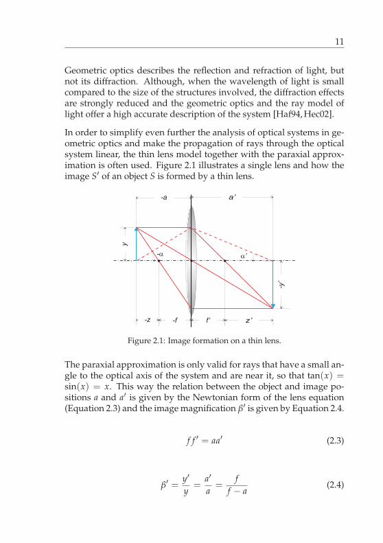
In order to simplify even further the analysis of optical systems in ge-ometric optics and make the propagation of rays through the opticalsystem linear, the thin lens model together with the paraxial approx-imation is often used. Figure 2.1 illustrates a single lens and how theimage S′ of an object S is formed by a thin lens.
-f f’-z z’
a’-a
y
-y’
a
-�
a’
�’
Figure 2.1: Image formation on a thin lens.
The paraxial approximation is only valid for rays that have a small an-gle to the optical axis of the system and are near it, so that tan(x) =sin(x) = x. This way the relation between the object and image po-sitions a and a′ is given by the Newtonian form of the lens equation(Equation 2.3) and the image magnification β′ is given by Equation 2.4.
f f ′ = aa′ (2.3)
β′ = y′
y=
a′
a=
ff − a
(2.4)
12
2.1.3 Ray-Tracing
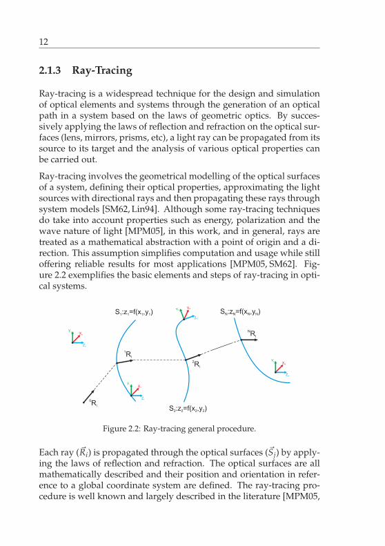
Ray-tracing is a widespread technique for the design and simulationof optical elements and systems through the generation of an opticalpath in a system based on the laws of geometric optics. By succes-sively applying the laws of reflection and refraction on the optical sur-faces (lens, mirrors, prisms, etc), a light ray can be propagated from itssource to its target and the analysis of various optical properties canbe carried out.
Ray-tracing involves the geometrical modelling of the optical surfacesof a system, defining their optical properties, approximating the lightsources with directional rays and then propagating these rays throughsystem models [SM62, Lin94]. Although some ray-tracing techniquesdo take into account properties such as energy, polarization and thewave nature of light [MPM05], in this work, and in general, rays aretreated as a mathematical abstraction with a point of origin and a di-rection. This assumption simplifies computation and usage while stilloffering reliable results for most applications [MPM05, SM62]. Fig-ure 2.2 exemplifies the basic elements and steps of ray-tracing in opti-cal systems.
Z0
Y0
X0
Z1
Y1
X1
Z2
Y2X2
ZN
YN
XN
0
Ri
1
Ri
2
Ri
N
Ri
S :z =f(x ,y )1 1 1 1
S :z =f(x ,y )2 2 2 2
S :z =f(x ,y )N N N N
Figure 2.2: Ray-tracing general procedure.
Each ray (�Ri) is propagated through the optical surfaces (�Sj) by apply-ing the laws of reflection and refraction. The optical surfaces are allmathematically described and their position and orientation in refer-ence to a global coordinate system are defined. The ray-tracing pro-cedure is well known and largely described in the literature [MPM05,
13
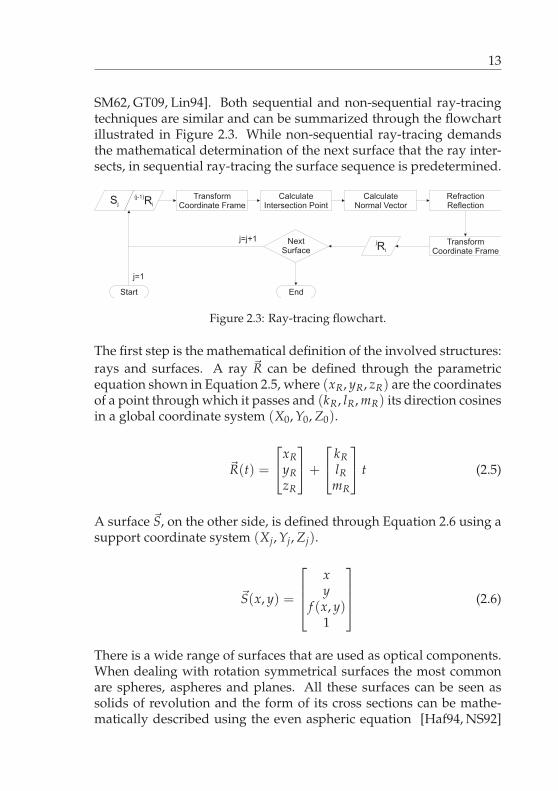
SM62, GT09, Lin94]. Both sequential and non-sequential ray-tracingtechniques are similar and can be summarized through the flowchartillustrated in Figure 2.3. While non-sequential ray-tracing demandsthe mathematical determination of the next surface that the ray inter-sects, in sequential ray-tracing the surface sequence is predetermined.
(j-1)
Ri
Sj
Transform
Coordinate Frame
Calculate
Intersection Point
Calculate
Normal Vector
Refraction
Reflection
j
Ri
Start End
Next
Surface
j=j+1
j=1
Transform
Coordinate Frame
Figure 2.3: Ray-tracing flowchart.
The first step is the mathematical definition of the involved structures:rays and surfaces. A ray �R can be defined through the parametricequation shown in Equation 2.5, where (xR, yR, zR) are the coordinatesof a point through which it passes and (kR, lR, mR) its direction cosinesin a global coordinate system (X0, Y0, Z0).
�R(t) =
⎡⎣xR
yRzR
⎤⎦+
⎡⎣ kR
lRmR
⎤⎦ t (2.5)
A surface �S, on the other side, is defined through Equation 2.6 using asupport coordinate system (Xj, Yj, Zj).
�S(x, y) =
⎡⎢⎢⎣
xy
f (x, y)1
⎤⎥⎥⎦ (2.6)
There is a wide range of surfaces that are used as optical components.When dealing with rotation symmetrical surfaces the most commonare spheres, aspheres and planes. All these surfaces can be seen assolids of revolution and the form of its cross sections can be mathe-matically described using the even aspheric equation [Haf94, NS92]
14
(Equation 2.7), where z is the height of the aspheric surface, r the ra-dial distance to the centre, C the surface curvature, K the conic con-stant and Ki the aspheric coefficients of the surface. The even asphericequation is widely used by optical manufacturers and optical designprograms to describe lenses [Haf94, Mar91, NS92].
z =Cr2
1 +√
1 − (1 + K)C2r2+ K2r2 + K4r4 + ... (2.7)
This way, the surface shape is fully defined using the parameters (C,K, K2, K4, ...) and the next step in describing the optical surface is to de-fine its position in the global coordinate system. Homogeneous coor-dinates and transformation matrices offer an optimal tool for this task,as they can represent rotation and translation in the form of matrixoperations. This way, any point from a surface �S can be represented inthe global coordinate system using Equation 2.8.
�S′(x, y) = T(α, β, γ, dx, dy, dz)
⎡⎢⎢⎣
xy
f (x, y)1
⎤⎥⎥⎦ (2.8)
,where T(α, β, γ, dx, dy, dz) is an homogeneous transformation definedby Equation 2.9 with the use of Euler angles [TV98].
⎧⎪⎪⎪⎪⎪⎪⎪⎪⎨⎪⎪⎪⎪⎪⎪⎪⎪⎩
T =
⎡⎢⎢⎢⎣
CαCγ + SαSβSγ −CβSγ −SαCγ + CαCβCγ dx
CαSγ − SαSβSγ CβCγ −SαSγ − CαCβCγ dy
SαCβ Sβ CαCβ dz
0 0 0 1
⎤⎥⎥⎥⎦
Sx = sin(x)Cx = cos(x)
(2.9)
The transformation T also enables the surface �S to move freely throughthe space, so that the mechanical movement of system componentscan then be described and simulated. Once the basic mathematical
15
structures are described, the next step is the definition of the ray-tracing operations shown in the flowchart in Figure 2.3. In sequentialray-tracing, the surface sequence is predetermined, so that the calcu-lation of the next surface in the optical path is not necessary. For theevaluation of the surface geometry, the calculation of the intersectionpoint between a surface and a ray is given by the solution of the vectorequation:
T�S(x, y)− �R(t) =�0 (2.10)
Nevertheless, computationally, Equation 2.10 can be rewritten in amore efficient way as shown in Equation 2.11. This way the evaluatedray is represented in the support coordinate frame and the number ofnecessary mathematical operation reduced.
�S(x, y)− T−1�R(t) = �S(x, y)− �R′(t) =�0 (2.11)
As the function f (x, y) can be any arbitrary function, a direct solutionis not always possible, so that the use of numerical methods offer amore flexible solution. The intersection point between the surface �Sand the ray (�R′) can then be determined by finding the parameter tthat minimizes Equation 2.12:
ε(t) =[z�R′ (t)− f
(x�R′ (t) , y�R′ (t)
)]2 (2.12)
Once the intersection point P�R′ is determined, the surface normal inthis point can be calculated as:
�N =
∣∣∣∣∣∣∣− ∂ f (x,y)
∂x− ∂ f (x,y)
∂y1
∣∣∣∣∣∣∣−1 ⎡
⎢⎣−∂ f (x,y)
∂x− ∂ f (x,y)
∂y1
⎤⎥⎦∣∣∣∣∣∣∣∣P�R′
(2.13)
The incident ray and the normal vector are now known, so that it isnow possible to calculate the angle between both vectors as:
16
⎧⎪⎪⎪⎪⎪⎪⎪⎪⎨⎪⎪⎪⎪⎪⎪⎪⎪⎩
θ�R′ ,�S = �N ·
⎡⎢⎣ k�R′
l�R′m�R′
⎤⎥⎦
�N�R′ ,�S = �N ×
⎡⎢⎣ k�R′
l�R′m�R′
⎤⎥⎦
(2.14)
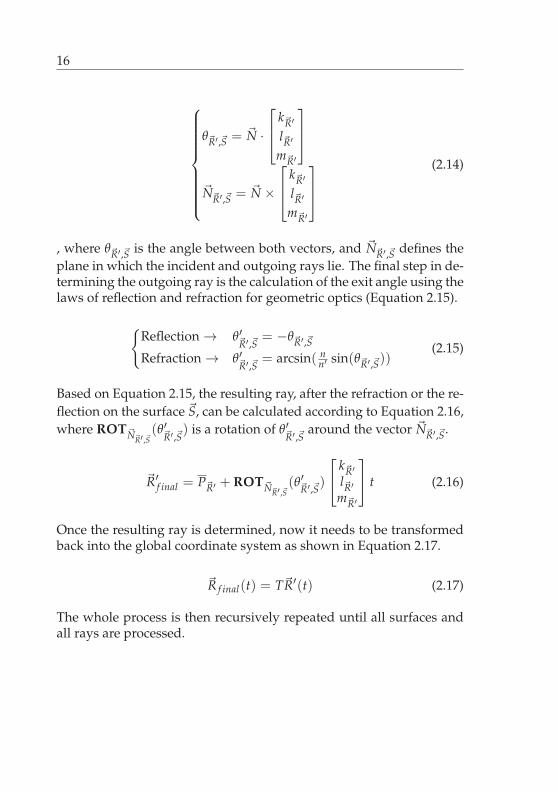
, where θ�R′ ,�S is the angle between both vectors, and �N�R′ ,�S defines theplane in which the incident and outgoing rays lie. The final step in de-termining the outgoing ray is the calculation of the exit angle using thelaws of reflection and refraction for geometric optics (Equation 2.15).
{Reflection → θ′�R′ ,�S = −θ�R′ ,�SRefraction → θ′�R′ ,�S = arcsin( n
n′ sin(θ�R′ ,�S))(2.15)
Based on Equation 2.15, the resulting ray, after the refraction or the re-flection on the surface �S, can be calculated according to Equation 2.16,where ROT�N�R′ ,�S
(θ′�R′ ,�S) is a rotation of θ′�R′ ,�S around the vector �N�R′ ,�S.
�R′f inal = P�R′ + ROT�N�R′ ,�S
(θ′�R′ ,�S)
⎡⎣ k�R′
l�R′m�R′
⎤⎦ t (2.16)
Once the resulting ray is determined, now it needs to be transformedback into the global coordinate system as shown in Equation 2.17.
�R f inal(t) = T�R′(t) (2.17)
The whole process is then recursively repeated until all surfaces andall rays are processed.
17
2.1.4 Optical Aberrations
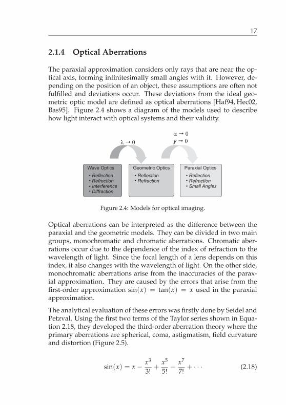
The paraxial approximation considers only rays that are near the op-tical axis, forming infinitesimally small angles with it. However, de-pending on the position of an object, these assumptions are often notfulfilled and deviations occur. These deviations from the ideal geo-metric optic model are defined as optical aberrations [Haf94, Hec02,Bas95]. Figure 2.4 shows a diagram of the models used to describehow light interact with optical systems and their validity.
Wave Optics
ReflectionRefractionInterferenceDiffraction
Geometric Optics
ReflectionRefraction
Paraxial Optics
ReflectionRefractionSmall Angles
���
���
y ��
Figure 2.4: Models for optical imaging.
Optical aberrations can be interpreted as the difference between theparaxial and the geometric models. They can be divided in two maingroups, monochromatic and chromatic aberrations. Chromatic aber-rations occur due to the dependence of the index of refraction to thewavelength of light. Since the focal length of a lens depends on thisindex, it also changes with the wavelength of light. On the other side,monochromatic aberrations arise from the inaccuracies of the parax-ial approximation. They are caused by the errors that arise from thefirst-order approximation sin(x) = tan(x) = x used in the paraxialapproximation.
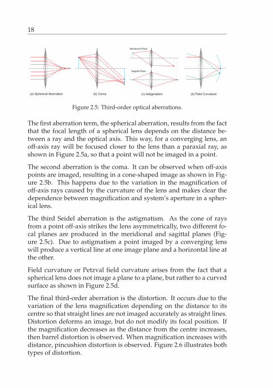
The analytical evaluation of these errors was firstly done by Seidel andPetzval. Using the first two terms of the Taylor series shown in Equa-tion 2.18, they developed the third-order aberration theory where theprimary aberrations are spherical, coma, astigmatism, field curvatureand distortion (Figure 2.5).
sin(x) = x − x3
3!+
x5
5!− x7
7!+ · · · (2.18)
18
Sagittal Plane
Meridional Plane
(a) Spherical Aberration (b) Coma (c) Astigmatism (d) Field Curvature
Figure 2.5: Third-order optical aberrations.
The first aberration term, the spherical aberration, results from the factthat the focal length of a spherical lens depends on the distance be-tween a ray and the optical axis. This way, for a converging lens, anoff-axis ray will be focused closer to the lens than a paraxial ray, asshown in Figure 2.5a, so that a point will not be imaged in a point.
The second aberration is the coma. It can be observed when off-axispoints are imaged, resulting in a cone-shaped image as shown in Fig-ure 2.5b. This happens due to the variation in the magnification ofoff-axis rays caused by the curvature of the lens and makes clear thedependence between magnification and system’s aperture in a spher-ical lens.
The third Seidel aberration is the astigmatism. As the cone of raysfrom a point off-axis strikes the lens asymmetrically, two different fo-cal planes are produced in the meridional and sagittal planes (Fig-ure 2.5c). Due to astigmatism a point imaged by a converging lenswill produce a vertical line at one image plane and a horizontal line atthe other.
Field curvature or Petzval field curvature arises from the fact that aspherical lens does not image a plane to a plane, but rather to a curvedsurface as shown in Figure 2.5d.
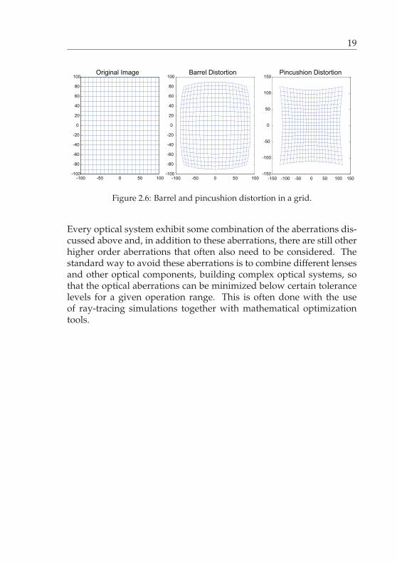
The final third-order aberration is the distortion. It occurs due to thevariation of the lens magnification depending on the distance to itscentre so that straight lines are not imaged accurately as straight lines.Distortion deforms an image, but do not modify its focal position. Ifthe magnification decreases as the distance from the centre increases,then barrel distortion is observed. When magnification increases withdistance, pincushion distortion is observed. Figure 2.6 illustrates bothtypes of distortion.
19
Figure 2.6: Barrel and pincushion distortion in a grid.
Every optical system exhibit some combination of the aberrations dis-cussed above and, in addition to these aberrations, there are still otherhigher order aberrations that often also need to be considered. Thestandard way to avoid these aberrations is to combine different lensesand other optical components, building complex optical systems, sothat the optical aberrations can be minimized below certain tolerancelevels for a given operation range. This is often done with the useof ray-tracing simulations together with mathematical optimizationtools.
20
2.2 Confocal Microscopy
Optical microscopy started in the 17th century in the Netherlands andis today one of the most widely used scientific tools worldwide [Rie88].The goal of optical microscopy is the use of optical systems to generatea magnified image of a sample and make different features from theseobjects visible. The generated image can then be observed directly bythe eye or with a camera.
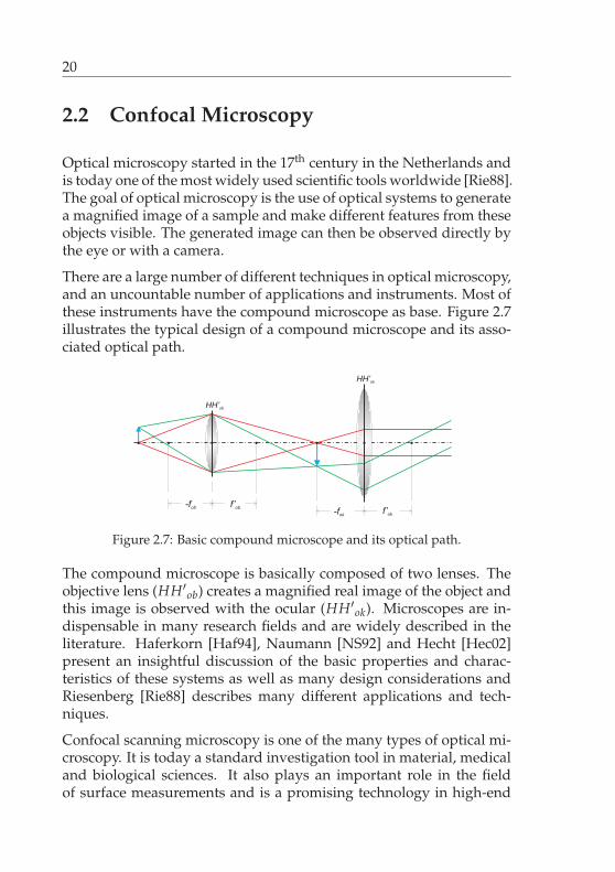
There are a large number of different techniques in optical microscopy,and an uncountable number of applications and instruments. Most ofthese instruments have the compound microscope as base. Figure 2.7illustrates the typical design of a compound microscope and its asso-ciated optical path.
HH’ob
HH’ok
-fob f’ob-fok
f’ok
Figure 2.7: Basic compound microscope and its optical path.
The compound microscope is basically composed of two lenses. Theobjective lens (HH′
ob) creates a magnified real image of the object andthis image is observed with the ocular (HH′
ok). Microscopes are in-dispensable in many research fields and are widely described in theliterature. Haferkorn [Haf94], Naumann [NS92] and Hecht [Hec02]present an insightful discussion of the basic properties and charac-teristics of these systems as well as many design considerations andRiesenberg [Rie88] describes many different applications and tech-niques.
Confocal scanning microscopy is one of the many types of optical mi-croscopy. It is today a standard investigation tool in material, medicaland biological sciences. It also plays an important role in the fieldof surface measurements and is a promising technology in high-end
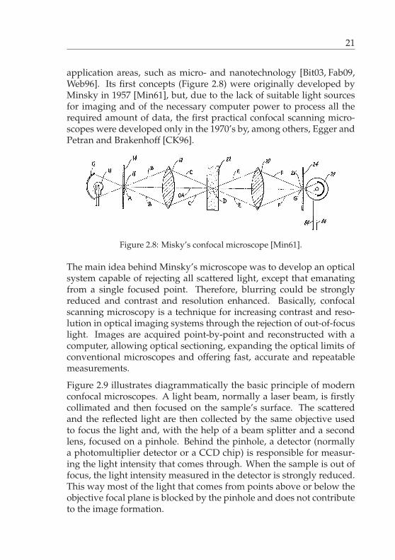
21
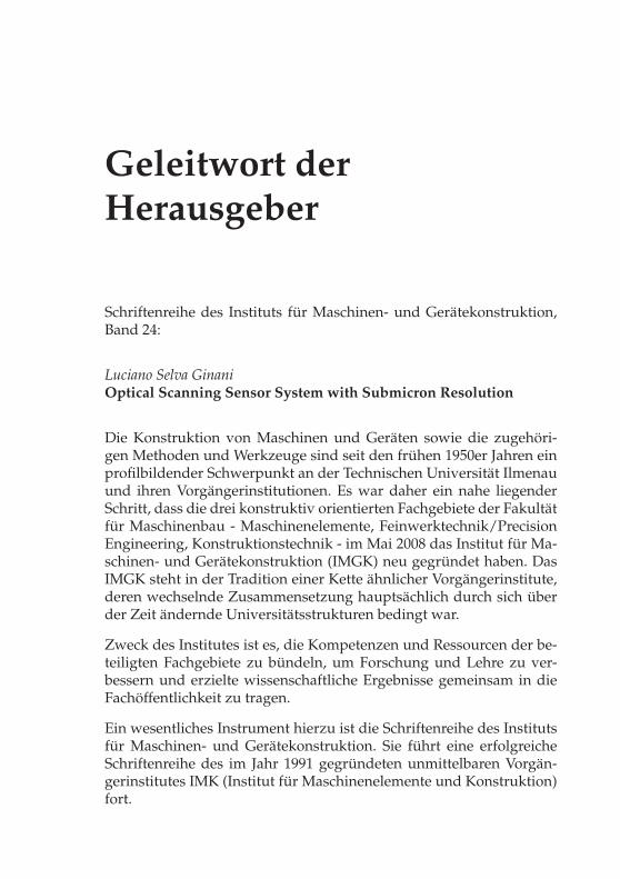
application areas, such as micro- and nanotechnology [Bit03, Fab09,Web96]. Its first concepts (Figure 2.8) were originally developed byMinsky in 1957 [Min61], but, due to the lack of suitable light sourcesfor imaging and of the necessary computer power to process all therequired amount of data, the first practical confocal scanning micro-scopes were developed only in the 1970’s by, among others, Egger andPetran and Brakenhoff [CK96].
Figure 2.8: Misky’s confocal microscope [Min61].
The main idea behind Minsky’s microscope was to develop an opticalsystem capable of rejecting all scattered light, except that emanatingfrom a single focused point. Therefore, blurring could be stronglyreduced and contrast and resolution enhanced. Basically, confocalscanning microscopy is a technique for increasing contrast and reso-lution in optical imaging systems through the rejection of out-of-focuslight. Images are acquired point-by-point and reconstructed with acomputer, allowing optical sectioning, expanding the optical limits ofconventional microscopes and offering fast, accurate and repeatablemeasurements.
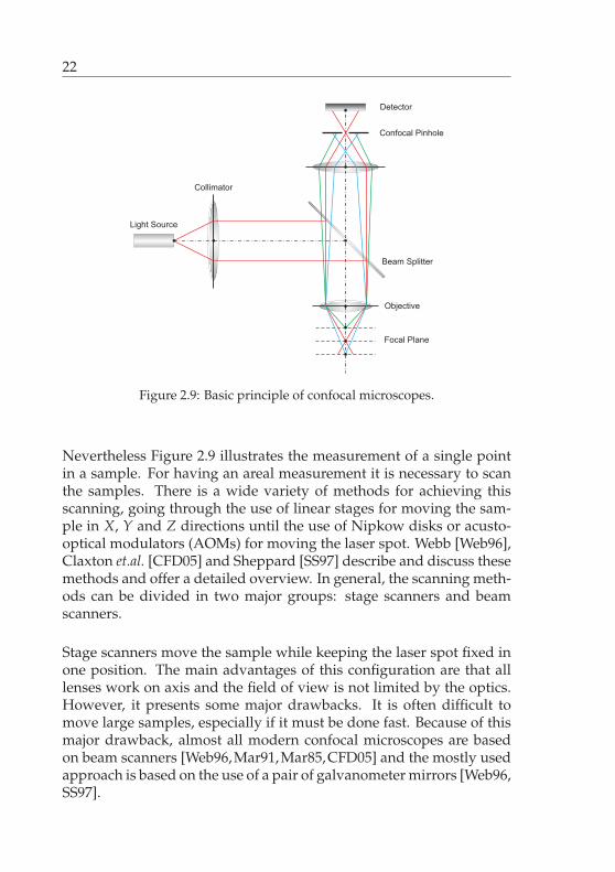
Figure 2.9 illustrates diagrammatically the basic principle of modernconfocal microscopes. A light beam, normally a laser beam, is firstlycollimated and then focused on the sample’s surface. The scatteredand the reflected light are then collected by the same objective usedto focus the light and, with the help of a beam splitter and a secondlens, focused on a pinhole. Behind the pinhole, a detector (normallya photomultiplier detector or a CCD chip) is responsible for measur-ing the light intensity that comes through. When the sample is out offocus, the light intensity measured in the detector is strongly reduced.This way most of the light that comes from points above or below theobjective focal plane is blocked by the pinhole and does not contributeto the image formation.
22
Collimator
Light Source
Objective
Confocal Pinhole
Detector
Beam Splitter
Focal Plane
Figure 2.9: Basic principle of confocal microscopes.
Nevertheless Figure 2.9 illustrates the measurement of a single pointin a sample. For having an areal measurement it is necessary to scanthe samples. There is a wide variety of methods for achieving thisscanning, going through the use of linear stages for moving the sam-ple in X, Y and Z directions until the use of Nipkow disks or acusto-optical modulators (AOMs) for moving the laser spot. Webb [Web96],Claxton et.al. [CFD05] and Sheppard [SS97] describe and discuss thesemethods and offer a detailed overview. In general, the scanning meth-ods can be divided in two major groups: stage scanners and beamscanners.
Stage scanners move the sample while keeping the laser spot fixed inone position. The main advantages of this configuration are that alllenses work on axis and the field of view is not limited by the optics.However, it presents some major drawbacks. It is often difficult tomove large samples, especially if it must be done fast. Because of thismajor drawback, almost all modern confocal microscopes are basedon beam scanners [Web96,Mar91,Mar85,CFD05] and the mostly usedapproach is based on the use of a pair of galvanometer mirrors [Web96,SS97].
23
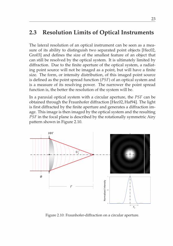
2.3 Resolution Limits of Optical Instruments
The lateral resolution of an optical instrument can be seen as a mea-sure of its ability to distinguish two separated point objects [Hec02,Gro03] and defines the size of the smallest feature of an object thatcan still be resolved by the optical system. It is ultimately limited bydiffraction. Due to the finite aperture of the optical system, a radiat-ing point source will not be imaged as a point, but will have a finitesize. The form, or intensity distribution, of this imaged point sourceis defined as the point spread function (PSF) of an optical system andis a measure of its resolving power. The narrower the point spreadfunction is, the better the resolution of the system will be.
In a paraxial optical system with a circular aperture, the PSF can beobtained through the Fraunhofer diffraction [Hec02, Haf94]. The lightis first diffracted by the finite aperture and generates a diffraction im-age. This image is then imaged by the optical system and the resultingPSF in the focal plane is described by the rotationally symmetric Airypattern shown in Figure 2.10.
0
0.5
1
HH’
f’
r0
Norm
alized Inte
nsity
�
Figure 2.10: Fraunhofer-diffraction on a circular aperture.
24
The size of the resulting Airy pattern will depend on the numericalaperture (NA) of the lens. The NA describes the ability of a lens togather light and is important to determine its resolution limits. It de-pends of the half aperture angle (θ) and the refraction index of themedium (n) and is defined as shown in Equation 2.19.
NA = n sin(θ) (2.19)
The most well known resolution criterion is the Rayleigh criterion. Itsays that for two incoherent point sources to be still resolved by anoptical instrument, the maxima of one of the imaged Airy disks mustbe at least coincident with the first minimum of the second Airy disk.This way the minimum separation between two features is given byEquation 2.20, where λ is the wavelength of the light and NA is thenumerical aperture of the optical system.
dmin =0.61λ
NA(2.20)
The Rayleigh criterion is considered a conservative measure of thespatial resolution of an optical instrument [Hec02, Gro03]. Anotherwidely used criterion is the Sparrow criterion [Hec02, GVY05]. It con-siders the fact that two Airy disks can still be detected as long as aminimum exists between their maxima. This way the smallest separa-tion between two points, so that both are still distinguishable is:
dmin =0.47λ
NA(2.21)
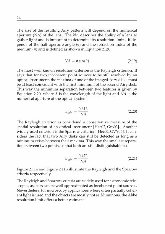
Figure 2.11a and Figure 2.11b illustrate the Rayleigh and the Sparrowcriteria respectively.
The Rayleigh and Sparrow criteria are widely used for astronomic tele-scopes, as stars can be well approximated as incoherent point sources.Nevertheless, for microscopy applications where often partially coher-ent light is used and the objects are mostly not self-luminous, the Abberesolution limit offers a better estimate.
25
Rayleigh
ResolutionLimit
Sparrow
Resolution Limit
Inte
nsity
a b
r0
Inte
nsity
Figure 2.11: Rayleigh and sparrow resolution criteria.
In order to estimate the resolution limit of optical instruments, ErnstAbbe used a periodic grating. The grating diffracts the light and, de-pending on the aperture angle of the optical system, different diffrac-tion orders are filtered. Abbe defined that for an image to be resolved,at least the 0th and the 1st diffraction orders should still be imaged bythe optical system. This way the resolution limit of an optical systemis given by Equation 2.22.
dmin =0.5λ
NA(2.22)
In the special case of confocal microscopy, the resolution can still beslightly improved. If the pinhole is chosen to have a radius smallerthan the radius of the Airy disk (r0), the diffraction of the light on thepinhole starts to have a significant influence on the system so that theresolution limit is improved as shown in Equation 2.23.
dmin =0.37λ
NA(2.23)
Nevertheless it is important to consider the fact that all the discussedtheoretical resolution limits consider the use of a perfect optical sys-tem without any optical aberrations, what in practice is not possible.Therefore, the resolution achieved by an optical instrument is alwaysinferior to its theoretical limit. For standard compound light micro-scopes with numerical apertures of approximately 1.0 and white lightillumination (λ ≈ 500nm), the best achievable resolution is around2μm.
26
2.4 Auto-focus in Optical Systems
Due to the overwhelming demand of the industry, especially in thefield of optical data storage (CD, DVD, MD, Blue-Ray), a large varietyof methods and sensors have been developed for focus point detec-tion [Mas05,Mar91,Coh87,MS97,CNY+00,The88]. The detection of thefocus error signal (FES) is a key task in those systems and many meth-ods such as the astigmatic method, the Foucault knife-edge method,the beam offset method, the critical angle prism method, the spot sizemethod have been adopted and are extensively described in the lit-erature. Most of those techniques rely on the use of a detection lensto create a secondary focused spot, so that deviations from the focus-ing on the sample cause a change in the shape, size or position of thesecondary spot.
From all these methods the two most widely used are the astigmaticand the Foucault knife-edge methods [Mas12, MS97, The88, Mer84].Barthel [Bar85], Theska [The88], Cohen [Coh87] and many other au-thors [Mar91, CNY+00, MMJ04, She93, HBVS03] have thoroughly de-scribed and studied these various focus point detection methods in theliterature, therefore in this chapter only the astigmatic and the knife-edge methods, as the most widely used ones, will be presented in de-tail.
2.4.1 Astigmatic Method
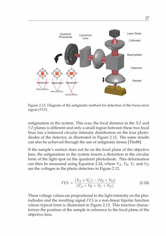
The astigmatic method, developed by Bricot [BL76] in 1976, is the mostused focus point detection method and offers a good compromise be-tween sensitivity and acquisition range [CNY+00]. The basic diagramof the astigmatic method is illustrated in Figure 2.12. The main ele-ments of the system are the light source, the collimation optics, thefocusing optics, the detection optics and the quadrant photodiode fordetecting the light intensity distribution.
A collimated light beam is focused on the sample’s surface and the re-flected light is collected by the same focusing optics. With the help of abeam splitter the light is directed towards the detection optics where acombination of a converging lens and a cylindrical lens focus the lightin a quadrant photodiode. The cylindrical lens is responsible for the
27
Laser Diode
Sample
Quadrant
Photodiode
Collimator
Objective
Beamsplitter
Cylindrical
Lens
A
B
C
D
A
B
C
D
A
B
C
D
Figure 2.12: Diagram of the astigmatic method for detection of the focus errorsignal (FES).
astigmatism in the system. This way, the focal distance in the XZ andYZ planes is different and only a small region between these two focallines has a balanced circular intensity distribution on the four photo-diodes of the detector, as illustrated in Figure 2.12. The same resultscan also be achieved through the use of astigmatic lenses [The88].
If the sample’s surface does not lie on the focal plane of the objectivelens, the astigmatism in the system inserts a distortion in the circularform of the light spot on the quadrant photodiode. This deformationcan then be measured using Equation 2.24, where VA, VB, VC and VDare the voltages in the photo detectors in Figure 2.12.
FES =(VA + VC)− (VB + VD)
(VA + VB + VC + VD)(2.24)
These voltage values are proportional to the light intensity on the pho-todiodes and the resulting signal FES is a non-linear bipolar functionwhose typical form is illustrated in Figure 2.13. This function charac-terizes the position of the sample in reference to the focal plane of theobjective lens.
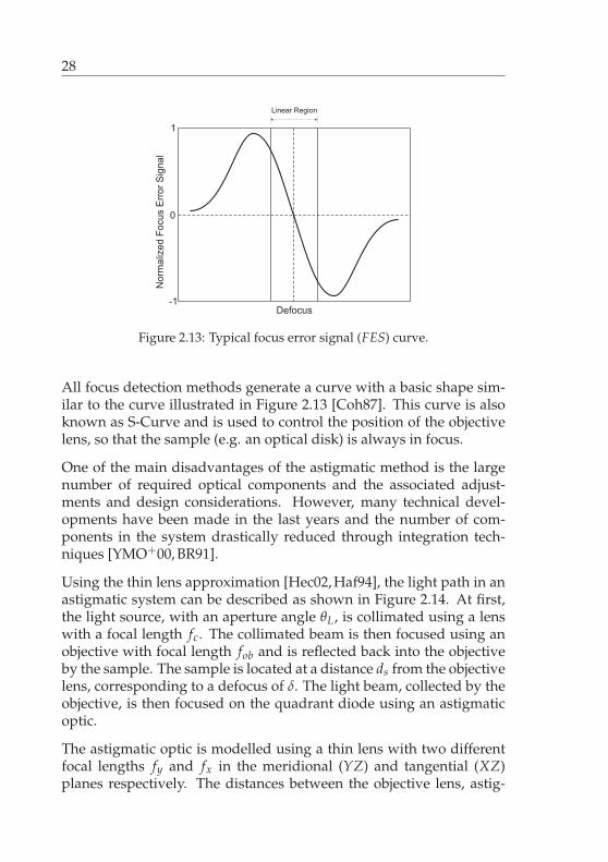
28
Defocus
No
rma
lize
d F
ocu
s E
rro
r S
ign
al
0
1
-1
Linear Region
Figure 2.13: Typical focus error signal (FES) curve.
All focus detection methods generate a curve with a basic shape sim-ilar to the curve illustrated in Figure 2.13 [Coh87]. This curve is alsoknown as S-Curve and is used to control the position of the objectivelens, so that the sample (e.g. an optical disk) is always in focus.
One of the main disadvantages of the astigmatic method is the largenumber of required optical components and the associated adjust-ments and design considerations. However, many technical devel-opments have been made in the last years and the number of com-ponents in the system drastically reduced through integration tech-niques [YMO+00, BR91].
Using the thin lens approximation [Hec02, Haf94], the light path in anastigmatic system can be described as shown in Figure 2.14. At first,the light source, with an aperture angle θL, is collimated using a lenswith a focal length fc. The collimated beam is then focused using anobjective with focal length fob and is reflected back into the objectiveby the sample. The sample is located at a distance ds from the objectivelens, corresponding to a defocus of δ. The light beam, collected by theobjective, is then focused on the quadrant diode using an astigmaticoptic.
The astigmatic optic is modelled using a thin lens with two differentfocal lengths fy and fx in the meridional (YZ) and tangential (XZ)planes respectively. The distances between the objective lens, astig-
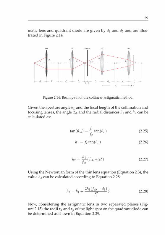
29
matic lens and quadrant diode are given by d1 and d2 and are illus-trated in Figure 2.14.
HH’co HH’ob HH’ob HH’s
h1 h1�
ob�
ob
h2
h3 ry
��-fc f ’c -fob f ’ob f ’ob f ’y-fob
-fy
�L
Sample
d1 d2
Figure 2.14: Beam path of the collinear astigmatic method.
Given the aperture angle θL and the focal length of the collimation andfocusing lenses, the angle θob and the radial distances h1 and h2 can becalculated as:
tan(θob) =fc
fotan(θL) (2.25)
h1 = fc tan(θL) (2.26)
h2 =h1
fob( fob + 2δ) (2.27)
Using the Newtonian form of the thin lens equation (Equation 2.3), thevalue h3 can be calculated according to Equation 2.28:
h3 = h1 +2h1( fob − d1)
f 2o
δ (2.28)
Now, considering the astigmatic lens in two separated planes (Fig-ure 2.15) the radii rx and ry of the light spot on the quadrant diode canbe determined as shown in Equation 2.29.
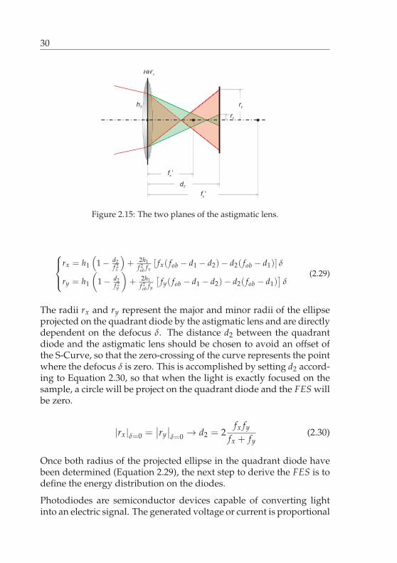
30
HH’s
h3 ry
f ’x
d2
f ’y
rx
Figure 2.15: The two planes of the astigmatic lens.
⎧⎪⎨⎪⎩
rx = h1
(1 − d2
f 2x
)+ 2h1
f 2ob fx
[ fx( fob − d1 − d2)− d2( fob − d1)] δ
ry = h1
(1 − d2
f 2y
)+ 2h1
f 2ob fy
[fy( fob − d1 − d2)− d2( fob − d1)
]δ
(2.29)
The radii rx and ry represent the major and minor radii of the ellipseprojected on the quadrant diode by the astigmatic lens and are directlydependent on the defocus δ. The distance d2 between the quadrantdiode and the astigmatic lens should be chosen to avoid an offset ofthe S-Curve, so that the zero-crossing of the curve represents the pointwhere the defocus δ is zero. This is accomplished by setting d2 accord-ing to Equation 2.30, so that when the light is exactly focused on thesample, a circle will be project on the quadrant diode and the FES willbe zero.
|rx|δ=0 =∣∣ry
∣∣δ=0 → d2 = 2
fx fy
fx + fy(2.30)
Once both radius of the projected ellipse in the quadrant diode havebeen determined (Equation 2.29), the next step to derive the FES is todefine the energy distribution on the diodes.
Photodiodes are semiconductor devices capable of converting lightinto an electric signal. The generated voltage or current is proportional
31
to the energy received and therefore to the energy distribution of theincident light on the detector active surface. Many different functionshave been used in the literature [CGLL84, Mas12, HBVS03] to approx-imate this distribution, but, as the mostly used light source for FESgeneration are laser diodes, a Gaussian distribution presents itself asthe most appropriate.
The energy distribution of the light spot on the detection surface canbe described with a two-dimensional Gaussian distribution [Hec02]as shown in Equation 2.31, where rx and ry are the radii of the beamwhere the energy is reduced by a factor of (1/e2) and (x, y) describe apoint in the detection surface of the quadrant diode.
I(x, y, δ) ∼ 1rx(δ)ry(δ)
exp(−2
((x − x0)
2
rx(δ)2 +(y − y0)
2
ry(δ)2
))(2.31)
x0 and y0 define the centre of the quadrant diode, so that, in the idealcase, when the laser diode is positioned exactly on the optical axis,their values are zero.
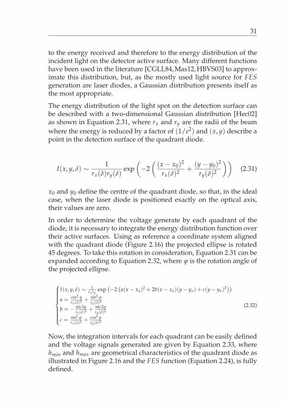
In order to determine the voltage generate by each quadrant of thediode, it is necessary to integrate the energy distribution function overtheir active surfaces. Using as reference a coordinate system alignedwith the quadrant diode (Figure 2.16) the projected ellipse is rotated45 degrees. To take this rotation in consideration, Equation 2.31 can beexpanded according to Equation 2.32, where ϕ is the rotation angle ofthe projected ellipse.
⎧⎪⎪⎪⎪⎪⎪⎨⎪⎪⎪⎪⎪⎪⎩
I(x, y, δ) ∼ 1rxry
exp(−2
(a(x − xo)2 + 2b(x − xo)(y − yo) + c(y − yo)2))
a = cos2 ϕ
rx(δ)2 + sin2 ϕ
ry(δ)2
b = − sin 2ϕ
rx(δ)2 + sin 2ϕ
ry(δ)2
c = sin2 ϕ
rx(δ)2 + cos2 ϕ
ry(δ)2
(2.32)
Now, the integration intervals for each quadrant can be easily definedand the voltage signals generated are given by Equation 2.33, wherehmin and hmax are geometrical characteristics of the quadrant diode asillustrated in Figure 2.16 and the FES function (Equation 2.24), is fullydefined.
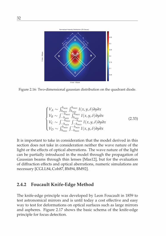
32
Normalized Intensity Distribution (2D-Gauss)
X Axis - Ellipse
Y A
xis
- E
llip
se
0.35
0.2
0.3
0.25
0.15
0.1
0.05
A
B
C
D
h max h
max
hn
mih
nm
i
Figure 2.16: Two-dimensional gaussian distribution on the quadrant diode.
⎧⎪⎪⎪⎪⎨⎪⎪⎪⎪⎩
VA ∼ ∫ hminhmax
∫ hmaxhmin
I(x, y, δ)∂y∂x
VB ∼ ∫ −hmax−hmin
∫ hmaxhmin
I(x, y, δ)∂y∂x
VC ∼ ∫ −hmax−hmin
∫ −hmin−hmax
I(x, y, δ)∂y∂x
VD ∼ ∫ hminhmax
∫ −hmin−hmax
I(x, y, δ)∂y∂x
(2.33)
It is important to take in consideration that the model derived in thissection does not take in consideration neither the wave nature of thelight or the effects of optical aberrations. The wave nature of the lightcan be partially introduced in the model through the propagation ofGaussian beams through thin lenses [Mas12], but for the evaluationof diffraction effects and optical aberrations, numeric simulations arenecessary [CGLL84, Coh87, BM94, BM92].
2.4.2 Foucault Knife-Edge Method
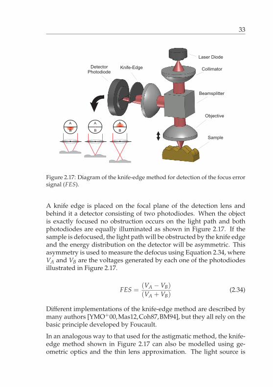
The knife-edge principle was developed by Leon Foucault in 1859 totest astronomical mirrors and is until today a cost effective and easyway to test for deformations on optical surfaces such as large mirrorsand aspheres. Figure 2.17 shows the basic schema of the knife-edgeprinciple for focus detection.
33
Laser Diode
Sample
Detector
PhotodiodeCollimator
Objective
Beamsplitter
Knife-Edge
A
B
A
B
A
B
Figure 2.17: Diagram of the knife-edge method for detection of the focus errorsignal (FES).
A knife edge is placed on the focal plane of the detection lens andbehind it a detector consisting of two photodiodes. When the objectis exactly focused no obstruction occurs on the light path and bothphotodiodes are equally illuminated as shown in Figure 2.17. If thesample is defocused, the light path will be obstructed by the knife edgeand the energy distribution on the detector will be asymmetric. Thisasymmetry is used to measure the defocus using Equation 2.34, whereVA and VB are the voltages generated by each one of the photodiodesillustrated in Figure 2.17.
FES =(VA − VB)
(VA + VB)(2.34)
Different implementations of the knife-edge method are described bymany authors [YMO+00,Mas12,Coh87,BM94], but they all rely on thebasic principle developed by Foucault.
In an analogous way to that used for the astigmatic method, the knife-edge method shown in Figure 2.17 can also be modelled using ge-ometric optics and the thin lens approximation. The light source is
34
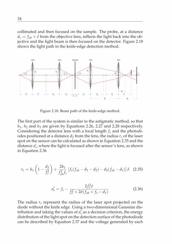
collimated and then focused on the sample. The probe, at a distanceds = fob + δ from the objective lens, reflects the light back into the ob-jective and the light beam is then focused on the detector. Figure 2.18shows the light path in the knife-edge detection method.
HH’co HH’ob HH’ob HH’s
h1 h1�
ob�
ob
h2
h3
��-fc f ’c -fob f ’ob f ’ob f ’s-fob
-fs
�L
Sample
d1 d2
rs
a ’s
Figure 2.18: Beam path of the knife-edge method.
The first part of the system is similar to the astigmatic method, so thath1, h2 and h3 are given by Equations 2.26, 2.27 and 2.28 respectively.Considering the detector lens with a focal length fs and the photodi-odes positioned at a distance d2 from the lens, the radius rs of the laserspot on the sensor can be calculated as shown in Equation 2.35 and thedistance a′s, where the light is focused after the sensor’s lens, as shownin Equation 2.36
rs = h1
(1 − d2
f 2s
)+
2h1
f 2ob fs
[ fs( fob − d1 − d2)− d2( fob − d1)] δ (2.35)
a′s = fs − 2 f 2s δ
f 2o + 2δ( fob + fs − d1)
(2.36)
The radius rs represent the radius of the laser spot projected on thediode without the knife edge. Using a two-dimensional Gaussian dis-tribution and taking the values of a′s as a decision criterion, the energydistribution of the light spot on the detection surface of the photodiodecan be described by Equation 2.37 and the voltage generated by each
35
one of the two photodiodes determined as shown in Equation 2.38.The FES is then given by Equation 2.34.
I(x, y, δ) ∼
⎧⎪⎪⎪⎪⎨⎪⎪⎪⎪⎩
1rs(δ)2 exp
(− 2
rs(δ)2
((x − x0)
2 + (y − y0)2)) if y ≤ 0, a′s ≤ fs
0 if y > 0, a′s < fs1
rs(δ)2 exp(− 2
rs(δ)2
((x − x0)
2 + (y − y0)2)) if y ≥ 0, a′s ≥ fs
0 if y < 0, a′s > fs
(2.37)
{VA ∼ ∫ hmax
−hmax
∫ hmaxhmin
I(x, y, δ)∂y∂x
VB ∼ ∫ hmax−hmax
∫ hmin−hmax
I(x, y, δ)∂y∂x(2.38)
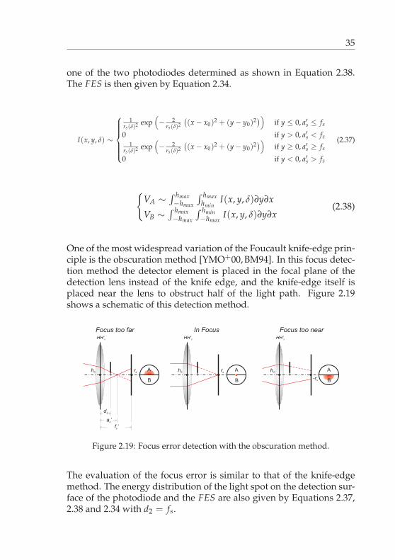
One of the most widespread variation of the Foucault knife-edge prin-ciple is the obscuration method [YMO+00, BM94]. In this focus detec-tion method the detector element is placed in the focal plane of thedetection lens instead of the knife edge, and the knife-edge itself isplaced near the lens to obstruct half of the light path. Figure 2.19shows a schematic of this detection method.
HH’s
h3
f ’s
d3
rs
a ’s
HH’s
h3 rs
HH’s
h3
-rs
A
B
A
B
A
B
In Focus Focus too nearFocus too far
Figure 2.19: Focus error detection with the obscuration method.
The evaluation of the focus error is similar to that of the knife-edgemethod. The energy distribution of the light spot on the detection sur-face of the photodiode and the FES are also given by Equations 2.37,2.38 and 2.34 with d2 = fs.
36
2.5 Optical Scanning
Focus point detection allows the measurement of the defocus in thesystem and therefore the measurement of the height of a single pointin a sample along the optical axis. Besides this axial measurement,in order to implement an areal measurement, a lateral scanning mustalso be implemented. As discussed in Chapter 2.2, optical scanningmethods can be divided in two major groups: stage scanners andbeam scanners. In this chapter a short overview on beam scannersis presented.
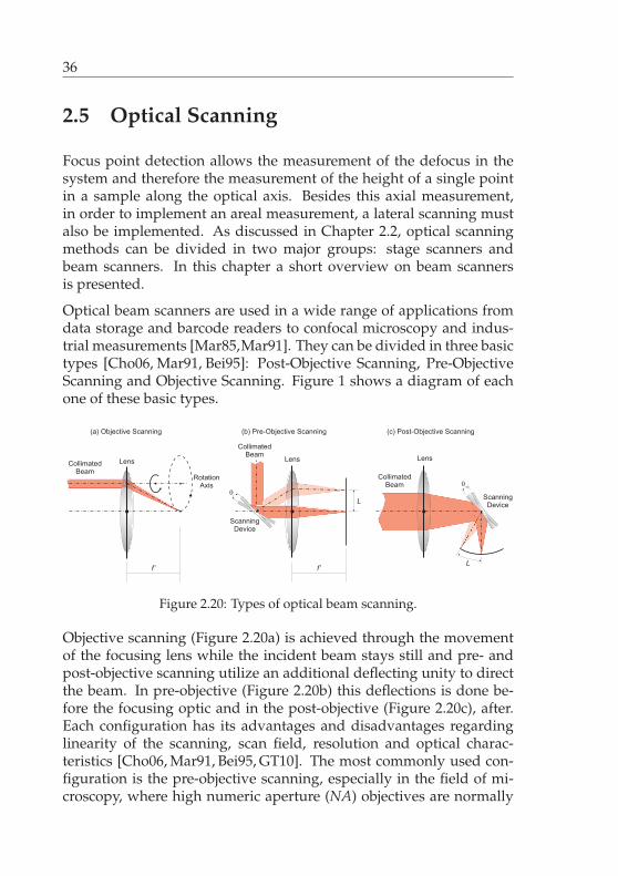
Optical beam scanners are used in a wide range of applications fromdata storage and barcode readers to confocal microscopy and indus-trial measurements [Mar85,Mar91]. They can be divided in three basictypes [Cho06, Mar91, Bei95]: Post-Objective Scanning, Pre-ObjectiveScanning and Objective Scanning. Figure 1 shows a diagram of eachone of these basic types.
L
�
�
Lf’
Collimated
Beam
Collimated
Beam
Collimated
Beam
LensLens Lens
Scanning
Device
Scanning
Device
Rotation
Axis
(a) Objective Scanning (b) Pre-Objective Scanning (c) Post-Objective Scanning
f’
Figure 2.20: Types of optical beam scanning.
Objective scanning (Figure 2.20a) is achieved through the movementof the focusing lens while the incident beam stays still and pre- andpost-objective scanning utilize an additional deflecting unity to directthe beam. In pre-objective (Figure 2.20b) this deflections is done be-fore the focusing optic and in the post-objective (Figure 2.20c), after.Each configuration has its advantages and disadvantages regardinglinearity of the scanning, scan field, resolution and optical charac-teristics [Cho06, Mar91, Bei95, GT10]. The most commonly used con-figuration is the pre-objective scanning, especially in the field of mi-croscopy, where high numeric aperture (NA) objectives are normally
37
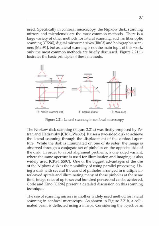
used. Specifically in confocal microscopy, the Nipkow disk, scanningmirrors and microlenses are the most common methods. There is alarge variety of other methods for lateral scanning, such as fiber opticscanning [CK96], digital mirror matrixes [Bit03] and holographic scan-ners [Mar91], but as lateral scanning is not the main topic of this work,only the most common methods are briefly discussed. Figure 2.21 il-lustrates the basic principle of these methods.
a Nipkow Scanning Disk b Scanning Mirror c Micro Lens
Figure 2.21: Lateral scanning in confocal microscopy.
The Nipkow disk scanning (Figure 2.21a) was firstly proposed by Pe-tran and Hadravsky [CK96,Web96]. It uses a two-sided disk to achievethe lateral scanning through the displacement of the confocal aper-ture. While the disk is illuminated on one of its sides, the image isobserved through a conjugate set of pinholes on the opposite side ofthe disk. In order to avoid alignment problems, a one sided variant,where the same aperture is used for illumination and imaging, is alsowidely used [CK96, SS97]. One of the biggest advantages of the useof the Nipkow disk is the possibility of using parallel processing. Us-ing a disk with several thousand of pinholes arranged in multiple in-terleaved spirals and illuminating many of these pinholes at the sametime, image rates of up to several hundred per second can be achieved.Corle and Kino [CK96] present a detailed discussion on this scanningtechnique.
The use of scanning mirrors is another widely used method for lateralscanning in confocal microscopy. As shown in Figure 2.21b, a colli-mated beam is deflected using a mirror. Considering the objective as
38
a perfect lens (paraxial approximation), the lateral displacement d ofthe focus spot is then given by Equation 2.39, where θ is the mirrorrotation angle and f the focal length of the objective.
d = f tan(2θ) (2.39)
The light reflected by the probe is then descanned by the same mirrorand focused on the imaging pinhole. Confocal microscopes employ-ing scanning mirrors often use laser sources for illumination and arecalled Confocal Laser Scanning Microscopes (CLSM). Typically, CLSMsystems include high-end objectives and additional sophisticated opti-cal systems to compensate for optical aberrations that arise as the sys-tem does not work on-axis. Other possibility to address this problem,based on the use of correction algorithms, is presented in Chapter 4.2and is one of the subjects addressed in this work.
Another possibility to achieve a lateral scanning is the use of microlensarrays. A microlens array is an arrangement of small lenses rangingfrom 1mm down to a few μm. With the use of such an array, thou-sands of small confocal systems can be build in parallel as shown inFigure 2.21c.
2.6 Modern Confocal Laser Scanning
Microscopy
Modern laser scanning microscope designs are centred on conven-tional upright or inverted optical microscope arrangements and theuse of standard high-end objective lenses with a high numerical aper-ture, for which there is a large design experience basis [Bit03, Fab09,Web96, XRJR07]. The basic diagram shown in Figure 2.9 does notrepresent the reality of these systems. Confocal laser scanning mi-croscopes are designed as complete stand-alone units with multipledetection and excitation channels, complex optics for beam condition-ing, high-end objective lenses, variable pinholes, beam scanners, aswell as a manifold of electronic components for operating and con-trolling these components.
39
Although a brief overview of these components was presented in pre-vious chapters, a detailed description is not in the scope of this work.Pawley [Paw06], Sheppard [SS97] and Corle [CK96] made a broaderstudy of traditional confocal laser scanning microscopy and describethoroughly each one of these components and their characteristics.
Modern confocal laser scanning microscopes are relatively large andare not intended for integration with other measuring systems. Ta-ble 2.1 shows a short summary of the typical size and scanning fre-quency of commercial available confocal laser scanning systems.
Table 2.1: Typical characteristics of commercial confocal scanning systems.
Property ValueFrame Rate 5 fps (500x500 Pixels)Size (350 × 450 × 500)mm
In order to measure the 3D topography of a sample, traditional con-focal microscopes need to acquire a stack of optical slices from thesample and merge them together [CFD05, Web96, SS97]. This way theacquisition times shown in Table 2.1 are normaly reduced by an aver-age factor of 40 or higher depending on the complexity of the sampleand the desired axial resolution.
As explained in Chapter 1.2, one of the objectives of this work is thesimplification and miniaturization of confocal laser scanning micro-scopes, making their integration with other systems viable. The com-bination of optical scanning techniques (Chapter 2.5) and auto-focusmethods (Chapter 2.4) offers new possibilities to the design of scan-ning microscopes and has a large potential for improving miniatur-ization, costs and measuring frequencies.

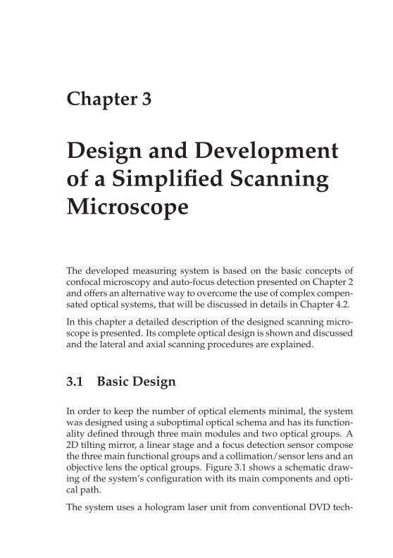
Chapter 3
Design and Developmentof a Simplified ScanningMicroscope
The developed measuring system is based on the basic concepts ofconfocal microscopy and auto-focus detection presented on Chapter 2and offers an alternative way to overcome the use of complex compen-sated optical systems, that will be discussed in details in Chapter 4.2.
In this chapter a detailed description of the designed scanning micro-scope is presented. Its complete optical design is shown and discussedand the lateral and axial scanning procedures are explained.
3.1 Basic Design
In order to keep the number of optical elements minimal, the systemwas designed using a suboptimal optical schema and has its function-ality defined through three main modules and two optical groups. A2D tilting mirror, a linear stage and a focus detection sensor composethe three main functional groups and a collimation/sensor lens and anobjective lens the optical groups. Figure 3.1 shows a schematic draw-ing of the system’s configuration with its main components and opti-cal path.
The system uses a hologram laser unit from conventional DVD tech-
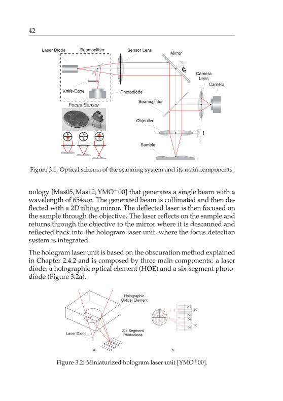
42
Focus Sensor
Laser Diode
Photodiode
Sensor LensMirror
Objective
Beamsplitter
Knife-Edge
Beamsplitter
Camera
Camera
Lens
Sample
A
B
A
B
A
B
Figure 3.1: Optical schema of the scanning system and its main components.
nology [Mas05, Mas12, YMO+00] that generates a single beam with awavelength of 654nm. The generated beam is collimated and then de-flected with a 2D tilting mirror. The deflected laser is then focused onthe sample through the objective. The laser reflects on the sample andreturns through the objective to the mirror where it is descanned andreflected back into the hologram laser unit, where the focus detectionsystem is integrated.
The hologram laser unit is based on the obscuration method explainedin Chapter 2.4.2 and is composed by three main components: a laserdiode, a holographic optical element (HOE) and a six-segment photo-diode (Figure 3.2a).
Six Segment
Photodiode
Holographic
Optical Element
Laser Diode
D1D2
D3
D4
D5D6
a b
Figure 3.2: Miniaturized hologram laser unit [YMO+00].
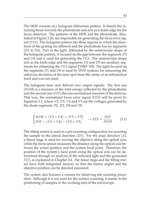
43
The HOE consists of a hologram diffraction pattern. It directs the re-turning beam towards the photodiode and acts as a knife-edge for thefocus detection. The patterns of the HOE and the photodiode, illus-trated in Figure 3.2b, are responsible for generating the focus error sig-nal (FES). The hologram pattern has three regions in which the direc-tions of the grating are different and the photodiode has six segments(D1 to D6). Part of the light, diffracted by the semicircular shape ofthe hologram pattern, is focused on the gap between the segments D3and D4 and is used for generating the FES. The semicircular shapeacts as the knife-edge and the segments D2 and D5 are auxiliary seg-ments for enhancing the FES signal [YMO+00]. The light focused onthe segments D1 and D6 is used by DVD systems for measuring thesideways deviation of the laser spot from the centre of an informationtrack and was not used.
The hologram laser unit delivers two output signals. The first one(SUM) is a measure of the total energy collected by the photodiodesand the second one (DIF) the non-normalized measure of the defocus.This way, the normalized focus error signal (FES) will be given byEquation 3.1, where V2, V3, V4 and V5 are the voltages generated bythe diode segments D2, D3, D4 and D5.
{SUM = (V2 + V4) + (V3 + V5)DIF = (V2 + V4)− (V3 + V5)
→ FES =DIF
SUM(3.1)
The tilting mirror is used in a pre-scanning configuration for scanningthe sample in the lateral direction (XY). For the axial direction (Z),a linear stage is used for moving the objective along the optical axis,while the focus sensor measures the distance along the optical axis be-tween the actual position and the system focal point. Therefore, theposition of the system’s focal point along the optical axis can be de-termined through an analysis of the reflected light and the generatedFES, as explained in Chapter 2.4. The linear stage and the tilting mir-ror have both integrated sensors, so that the mirror angles and theobjective position can be directed measured.
The system also features a camera for observing the scanning proce-dure. Although it is not used for the surface scanning, it assists in thepositioning of samples in the working area of the microscope.
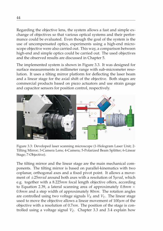
44
Regarding the objective lens, the system allows a fast and simple ex-change of objectives so that various optical systems and their perfor-mance could be evaluated. Even though the goal of the system is theuse of uncompensated optics, experiments using a high-end micro-scope objective were also carried out. This way, a comparison betweenhigh-end and simple optics could be carried out. The used objectivesand the observed results are discussed in Chapter 5.
The implemented system is shown in Figure 3.3. It was designed forsurface measurements in millimeter range with sub-micrometer reso-lution. It uses a tilting mirror platform for deflecting the laser beamand a linear stage for the axial shift of the objective. Both stages arecommercial products based on piezo actuators and use strain gaugeand capacitor sensors for position control, respectively.
1
2
3
4
5
67
Figure 3.3: Developed laser scanning microscope (1-Hologram Laser Unit; 2-Tilting Mirror; 3-Camera Lens; 4-Camera; 5-Polarized Beam Splitter; 6-LinearStage; 7-Objective).
The tilting mirror and the linear stage are the main mechanical com-ponents. The tilting mirror is based on parallel-kinematics with twocoplanar, orthogonal axes and a fixed pivot point. It allows a move-ment of ±25mrad around both axes with a resolution of 5μrad, whiche.g. together with a 8.225mm focal length objective offers, accordingto Equation 2.39, a lateral scanning area of approximately 0.8mm ×0.8mm and a step width of approximately 80nm. The rotation anglesare controlled using two voltage signals VX and VY. The linear stageused to move the objective allows a linear movement of 100μm of theobjective with a resolution of 0.7nm. The position of the stage is con-trolled using a voltage signal VZ. Chapter 3.3 and 3.4 explain how
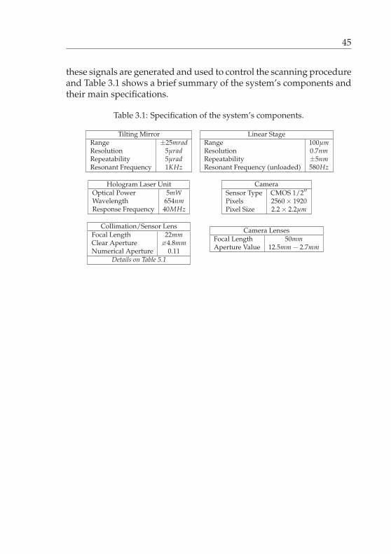
45
these signals are generated and used to control the scanning procedureand Table 3.1 shows a brief summary of the system’s components andtheir main specifications.
Table 3.1: Specification of the system’s components.
Tilting MirrorRange ±25mradResolution 5μradRepeatability 5μradResonant Frequency 1KHz
Linear StageRange 100μmResolution 0.7nmRepeatability ±5nmResonant Frequency (unloaded) 580Hz
Hologram Laser UnitOptical Power 5mWWavelength 654nmResponse Frequency 40MHz
CameraSensor Type CMOS 1/2′′Pixels 2560 × 1920Pixel Size 2.2 × 2.2μm
Collimation/Sensor LensFocal Length 22mmClear Aperture �4.8mmNumerical Aperture 0.11
Details on Table 5.1
Camera LensesFocal Length 50mmAperture Value 12.5mm − 2.7mm
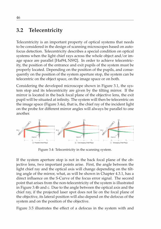
46
3.2 Telecentricity
Telecentricity is an important property of optical systems that needsto be considered in the design of scanning microscopes based on auto-focus detection. Telecentricity describes a special condition on opticalsystems when the light chief rays across the whole object and/or im-age space are parallel [Haf94, NS92]. In order to achieve telecentric-ity, the position of the entrance and exit pupils of the system must beproperly located. Depending on the position of the pupils, and conse-quently on the position of the system aperture stop, the system can betelecentric on the object space, on the image space or on both.
Considering the developed microscope shown in Figure 3.1, the sys-tem stop and its telecentricity are given by the tilting mirror. If themirror is located in the back focal plane of the objective lens, the exitpupil will be situated at infinity. The system will then be telecentric onthe image space (Figure 3.4a), that is, the chief ray of the incident lighton the probe for different mirror angles will always be parallel to oneanother.
HH’ob
Mirror
Objective
f’ob-fob
HH’ob
Mirror
Objective
f’ob-fob
HH’ob
Mirror
Objective
f’ob-fob
b ca Parallel Chief Rays Converging Chief Rays Diverging Chief Rays
Figure 3.4: Telecentricity in the scanning system.
If the system aperture stop is not in the back focal plane of the ob-jective lens, two important points arise. First, the angle between thelight chief ray and the optical axis will change depending on the tilt-ing angle of the mirror, what, as will be shown in Chapter 4.3.1, has adirect influence on the S-Curve of the focus error signal. The secondpoint that arises from the non-telecentricity of the system is illustratedin Figure 3.4b and c. Due to the angle between the optical axis and thechief ray, if the projected laser spot does not lie on the focal plane ofthe objective, its lateral position will also depend on the defocus of thesystem and on the position of the objective.
Figure 3.5 illustrates the effect of a defocus in the system with and
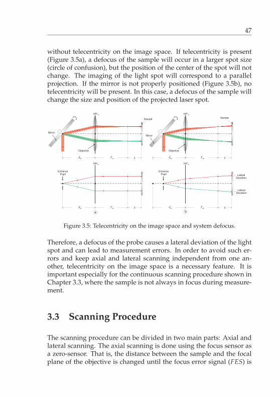
47
without telecentricity on the image space. If telecentricity is present(Figure 3.5a), a defocus of the sample will occur in a larger spot size(circle of confusion), but the position of the center of the spot will notchange. The imaging of the light spot will correspond to a parallelprojection. If the mirror is not properly positioned (Figure 3.5b), notelecentricity will be present. In this case, a defocus of the sample willchange the size and position of the projected laser spot.
HH’ob
Mirror
Objective
f’ob-fob
HH’ob
Mirror
Objective
f’ob-fob� �
SampleSample
f’ob-fob
HH’ob
f’ob-fob
ba
� �
HH’ob
Entrance
Pupil
Entrance
Pupil Lateral
Deviation
Lateral
Deviation
Figure 3.5: Telecentricity on the image space and system defocus.
Therefore, a defocus of the probe causes a lateral deviation of the lightspot and can lead to measurement errors. In order to avoid such er-rors and keep axial and lateral scanning independent from one an-other, telecentricity on the image space is a necessary feature. It isimportant especially for the continuous scanning procedure shown inChapter 3.3, where the sample is not always in focus during measure-ment.
3.3 Scanning Procedure
The scanning procedure can be divided in two main parts: Axial andlateral scanning. The axial scanning is done using the focus sensor asa zero-sensor. That is, the distance between the sample and the focalplane of the objective is changed until the focus error signal (FES) is
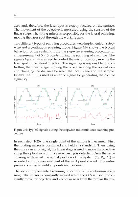
48
zero and, therefore, the laser spot is exactly focused on the surface.The movement of the objective is measured using the sensors of thelinear stage. The tilting mirror is responsible for the lateral scanning,moving the laser spot through the working area.
Two different types of scanning procedures were implemented: a step-wise and a continuous scanning mode. Figure 3.6a shows the typicalbehaviour of the system during the stepwise scanning procedure fora measurement of 5 × 5 points during the scanning of a sample. Thesignals VX and VY are used to control the mirror position, moving thelaser spot in the lateral direction. The signal VZ is responsible for con-trolling the linear stage, moving the objective along the optical axisand changing the distance between the focal plane and the sample.Finally, the FES is used as an error signal for generating the controlsignal VZ.
1
VX
VY
VZ
FES
Time
Sca
led
Syste
mS
ign
als
1110 2120
2
3
4
65 1615
7 14
8 13
129
18
17
19 22
23
24
25
1
VX
VY
VZ
FES
Time
Sca
led
Syste
mS
ign
als
1110 2120
2
3
4
65 1615
7 14
8 13
129
18
17
19 22
23
24
25
(a) (b)
Figure 3.6: Typical signals during the stepwise and continuous scanning pro-cedure.
In each step (1-25), one single point of the sample is measured. Firstthe rotating mirror is positioned and held at a standstill. Then, usingthe FES as an error signal, the linear stage is used to move the objectivealong the optical axis until a zero-crossing is detected. Once the zero-crossing is detected the actual position of the system (θx, θy, Δz) isrecorded and the measurement of the next point started. The entireprocess is repeated until all points are measured.
The second implemented scanning procedure is the continuous scan-ning. The mirror is constantly moved while the FES is used to con-stantly move the objective and keep it as near from the zero as the res-
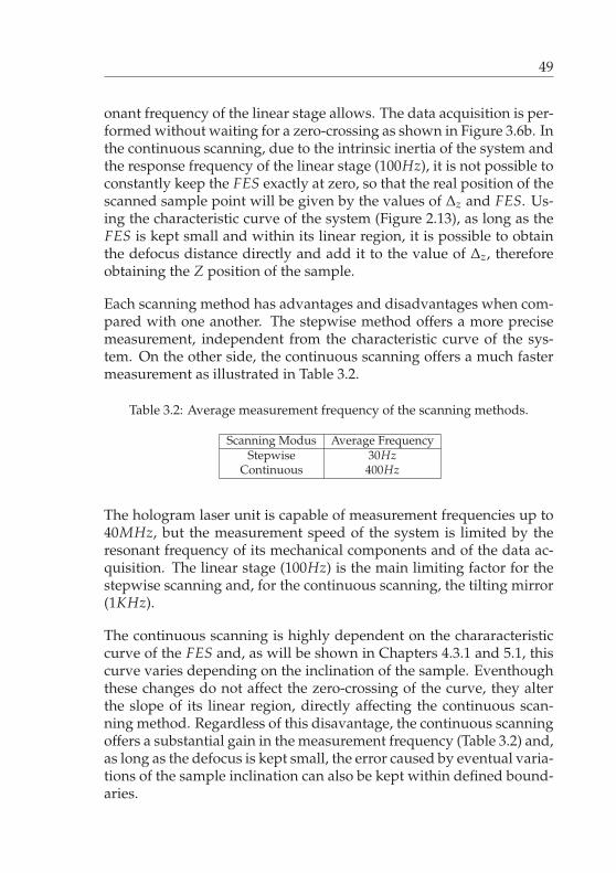
49
onant frequency of the linear stage allows. The data acquisition is per-formed without waiting for a zero-crossing as shown in Figure 3.6b. Inthe continuous scanning, due to the intrinsic inertia of the system andthe response frequency of the linear stage (100Hz), it is not possible toconstantly keep the FES exactly at zero, so that the real position of thescanned sample point will be given by the values of Δz and FES. Us-ing the characteristic curve of the system (Figure 2.13), as long as theFES is kept small and within its linear region, it is possible to obtainthe defocus distance directly and add it to the value of Δz, thereforeobtaining the Z position of the sample.
Each scanning method has advantages and disadvantages when com-pared with one another. The stepwise method offers a more precisemeasurement, independent from the characteristic curve of the sys-tem. On the other side, the continuous scanning offers a much fastermeasurement as illustrated in Table 3.2.
Table 3.2: Average measurement frequency of the scanning methods.
Scanning Modus Average FrequencyStepwise 30Hz
Continuous 400Hz
The hologram laser unit is capable of measurement frequencies up to40MHz, but the measurement speed of the system is limited by theresonant frequency of its mechanical components and of the data ac-quisition. The linear stage (100Hz) is the main limiting factor for thestepwise scanning and, for the continuous scanning, the tilting mirror(1KHz).
The continuous scanning is highly dependent on the chararacteristiccurve of the FES and, as will be shown in Chapters 4.3.1 and 5.1, thiscurve varies depending on the inclination of the sample. Eventhoughthese changes do not affect the zero-crossing of the curve, they alterthe slope of its linear region, directly affecting the continuous scan-ning method. Regardless of this disavantage, the continuous scanningoffers a substantial gain in the measurement frequency (Table 3.2) and,as long as the defocus is kept small, the error caused by eventual varia-tions of the sample inclination can also be kept within defined bound-aries.
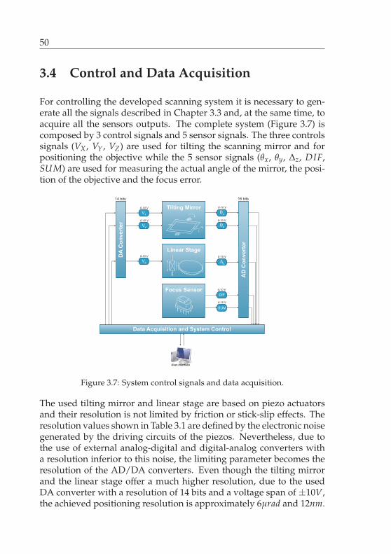
50
3.4 Control and Data Acquisition
For controlling the developed scanning system it is necessary to gen-erate all the signals described in Chapter 3.3 and, at the same time, toacquire all the sensors outputs. The complete system (Figure 3.7) iscomposed by 3 control signals and 5 sensor signals. The three controlssignals (VX , VY, VZ) are used for tilting the scanning mirror and forpositioning the objective while the 5 sensor signals (θx, θy, Δz, DIF,SUM) are used for measuring the actual angle of the mirror, the posi-tion of the objective and the focus error.
Tilting Mirror
�y
Linear Stage
Focus Sensor
�z
�x
Vy
Vz
Vx
SUM
DIF
DA
Co
nv
ert
er
0-10 V
0-10 V
0-10 V
0-10 V
0-10 V
0-10 V
0-10 V
0-10 V
AD
Co
nv
ert
er
Data Acquisition and System Control
14 bits 16 bits
User Interface
Figure 3.7: System control signals and data acquisition.
The used tilting mirror and linear stage are based on piezo actuatorsand their resolution is not limited by friction or stick-slip effects. Theresolution values shown in Table 3.1 are defined by the electronic noisegenerated by the driving circuits of the piezos. Nevertheless, due tothe use of external analog-digital and digital-analog converters witha resolution inferior to this noise, the limiting parameter becomes theresolution of the AD/DA converters. Even though the tilting mirrorand the linear stage offer a much higher resolution, due to the usedDA converter with a resolution of 14 bits and a voltage span of ±10V,the achieved positioning resolution is approximately 6μrad and 12nm.

51
The used AD converter has a slightly better resolution of 16 bits andboth of them have a maximal acquisition frequency of 10KHz. Ta-ble 3.3 shows the resolution limits imposed by the AD/DA converters.
Table 3.3: Resolution limits of the used AD/DA converters.
Variable Positioning Resolution Measuring Resolution Voltage Span(14 bits) (16 bits)θx 6μrad 1.5μrad ±10Vθy 6μrad 1.5μrad ±10VΔz 12nm 3nm ±10V
DIF − 0.3mV ±10VSUM − 0.3mV ±10V

Chapter 4
Modelling, Simulation andCalibration
The use of simple uncompensated lenses has always been avoided inscanning microscopy, as it inserts optical aberrations in the system,generates asymmetries in the focus error signal and deteriorates over-all performance. The traditional way of solving this problem, as men-tioned in previous chapters, is to improve the optical system such thatit works as a near-perfect lens, but that comes with the price of large,heavy and costly optics with shorter working distances.
Thanks to advances made in modern computing power, it is now pos-sible to consider unconventional alternatives to optics optimization.The developed scanning microscope presented in Chapter 3 aims atthe development of a simple and versatile system with the use of sub-optimal optics. Laser scanning microscopy is a technique that acquiresdata from the surface point to point, so that the measurement errorscaused by optical aberration at each measuring point can be predictedor measured. With previous knowledge of the occurring errors, it isthen possible to correct these errors computationally. This allows theuse of simpler optics in scanning systems, reducing overall size andweight, raising system dynamics and reducing costs, without signif-icant losses in accuracy. The use of simpler optics also facilitates theintegration of scanning devices in different applications. With smallersizes and longer working distances, scanning devices can be furtherminiaturized and easily integrated in different systems, allowing theiruse in applications such as parallel scanning, collision detection ofcantilevers and sensor fusion.
54
Nevertheless, it is important to note that the use of computer cor-rection strategies without any optical compensation also bring draw-backs to the system. The achievable lateral resolution of the opticalsystem as well as the system’s sensitivity will be inferior in compar-ison with a fully compensated system. Nevertheless, these issues donot render the use of simple optics and computer based correctionsunviable. The combination of traditional optics optimization withcomputer based correction offer more flexibility for the optical designand the task of error handling can be divided between optical com-pensation and computational correction.
In this chapter the complete modelling of the system is presented to-gether with a detailed description of the error correction strategies im-plemented.
4.1 Correction vs Compensation
Before describing the error correction strategies used, it is importantto properly define the use of the technical terms "compensation" and"correction". These terms are often incorrectly used in the literature asinterchangeable and are therefore more precisely defined in this sec-tion.
According to the Oxford dictionary, compensation can be defined assomething that counterbalances or makes up for an undesirable or un-welcome state of affairs, while correction is a quantity adjusting a nu-merical result to allow for a departure from standard conditions. Al-though both definitions may sound similar, they present a conceptualdifference. Compensation acts on an existing error, or undesired effect,continuously working against the error itself, while correction acts onthe obtained results, trying to adjust them to remove the influence ofthe errors through calculation.
In the scope of optical systems, compensation can be defined as hard-ware modifications such as changes of lens curvature, the addition ofan optical filter or aperture or the adjustment of system alignment.That means compensation alters the signals captured by the used sen-sors (photodiodes, CCD Matrices, etc.). On the other side, correctionuses the measured data signals and manipulates them in order to re-
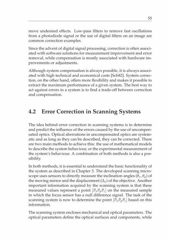
55
move undesired effects. Low-pass filters to remove fast oscillationsfrom a photodiode signal or the use of digital filters on an image arecommon correction examples.
Since the advent of digital signal processing, correction is often associ-ated with software solutions for measurement improvement and errorremoval, while compensation is mostly associated with hardware im-provements or adjustments.
Although system compensation is always possible, it is always associ-ated with high technical and economical costs [Sch82]. System correc-tion, on the other hand, offers more flexibility and makes it possible toextract the maximum performance of a given system. The best way toact against errors in a system is to find a trade-off between correctionand compensation.
4.2 Error Correction in Scanning Systems
The idea behind error correction in scanning systems is to determineand predict the influence of the errors caused by the use of uncompen-sated optics. Optical aberrations in uncompensated optics are system-atic and as long as they can be described, they can be corrected. Thereare two main methods to achieve this: the use of mathematical modelsto describe the system behaviour, or the experimental measurement ofthe system’s behaviour. A combination of both methods is also a pos-sibility.
In both methods, it is essential to understand the basic functionality ofthe system as described in Chapter 3. The developed scanning micro-scope uses sensors to directly measure the inclination angles (θx, θy) ofthe moving mirror and the displacement (Δz) of the objective. Anotherimportant information acquired by the scanning system is that thesemeasured values represent a point [PxPyPz] on the measured samplein which the focus sensor has a null difference signal. The task of thescanning system is now to determine the point [PxPyPz] based on thisinformation.
The scanning system encloses mechanical and optical parameters. Theoptical parameters define the optical surfaces and components, while
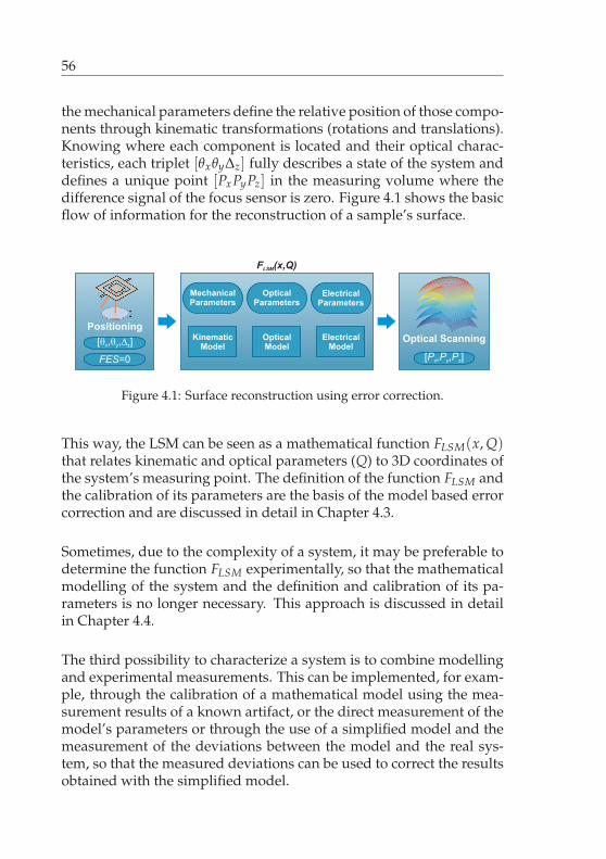
56
the mechanical parameters define the relative position of those compo-nents through kinematic transformations (rotations and translations).Knowing where each component is located and their optical charac-teristics, each triplet [θxθyΔz] fully describes a state of the system anddefines a unique point [PxPyPz] in the measuring volume where thedifference signal of the focus sensor is zero. Figure 4.1 shows the basicflow of information for the reconstruction of a sample’s surface.
Positioning
MechanicalParameters
OpticalParameters
ElectricalParameters
KinematicModel
OpticalModel
ElectricalModel
FES=0
[�,�,�]x y z
Optical Scanning
[P ,P ,P ]x y z
F (x,Q)LSM
Figure 4.1: Surface reconstruction using error correction.
This way, the LSM can be seen as a mathematical function FLSM(x, Q)that relates kinematic and optical parameters (Q) to 3D coordinates ofthe system’s measuring point. The definition of the function FLSM andthe calibration of its parameters are the basis of the model based errorcorrection and are discussed in detail in Chapter 4.3.
Sometimes, due to the complexity of a system, it may be preferable todetermine the function FLSM experimentally, so that the mathematicalmodelling of the system and the definition and calibration of its pa-rameters is no longer necessary. This approach is discussed in detailin Chapter 4.4.
The third possibility to characterize a system is to combine modellingand experimental measurements. This can be implemented, for exam-ple, through the calibration of a mathematical model using the mea-surement results of a known artifact, or the direct measurement of themodel’s parameters or through the use of a simplified model and themeasurement of the deviations between the model and the real sys-tem, so that the measured deviations can be used to correct the resultsobtained with the simplified model.
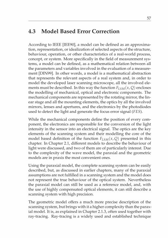
57
4.3 Model Based Error Correction
According to IEEE [IEE90], a model can be defined as an approxima-tion, representation, or idealization of selected aspects of the structure,behaviour, operation, or other characteristics of a real-world process,concept, or system. More specifically in the field of measurement sys-tems, a model can be defined, as a mathematical relation between allthe parameters and variables involved in the evaluation of a measure-ment [DIN99]. In other words, a model is a mathematical abstractionthat represents the relevant aspects of a real system and, in order tomodel the developed laser scanning microscope, all the involved ele-ments must be described. In this way the function FLSM(x, Q) enclosesthe modelling of mechanical, optical and electronic components. Themechanical components are represented by the rotating mirror, the lin-ear stage and all the mounting elements, the optics by all the involvedmirrors, lenses and apertures, and the electronics by the photodiodesused to detect the light and generate the focus error signal (FES).
While the mechanical components define the position of every com-ponent, the electronics are responsible for the conversion of the lightintensity in the sensor into an electrical signal. The optics are the keyelements of the scanning system and their modelling the core of themodel based definition of the function FLSM(x, Q) presented in thischapter. In Chapter 2.1, different models to describe the behaviour oflight were discussed, and two of them are of particularly interest. Dueto the complexity of the wave model, the paraxial and the geometricmodels are in praxis the most convenient ones.
Using the paraxial model, the complete scanning system can be easilydescribed, but, as discussed in earlier chapters, many of the paraxialassumptions are not fulfilled in a scanning system and the model doesnot represent the true behaviour of the optical system. Neverthelessthe paraxial model can still be used as a reference model, and, withthe use of highly compensated optical elements, it can still describe ascanning system with high precision.
The geometric model offers a much more precise description of thescanning system, but brings with it a higher complexity than the parax-ial model. It is, as explained in Chapter 2.1.3, often used together withray-tracing. Ray-tracing is a widely used and established technique
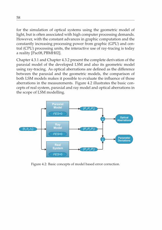
58
for the simulation of optical systems using the geometric model oflight, but is often associated with high computer processing demands.However, with the constant advances in graphic computation and theconstantly increasing processing power from graphic (GPU) and cen-tral (CPU) processing units, the interactive use of ray-tracing is todaya reality [Pac08, PBMH02].
Chapter 4.3.1 and Chapter 4.3.2 present the complete derivation of theparaxial model of the developed LSM and also its geometric modelusing ray-tracing. As optical aberrations are defined as the differencebetween the paraxial and the geometric models, the comparison ofboth LSM models makes it possible to evaluate the influence of thoseaberrations in the measurements. Figure 4.2 illustrates the basic con-cepts of real system, paraxial and ray model and optical aberrations inthe scope of LSM modelling.
ParaxialModel
FES=0
[�,�,�]x y z
RealSystem
FES=0
RayModel
FES=0
[P ,P ,P ]x y z
[P ,P ,P ]x y z
[P ,P ,P ]x y z
+-
+- Optical
Aberrations
ParameterDeviations
Figure 4.2: Basic concepts of model based error correction.
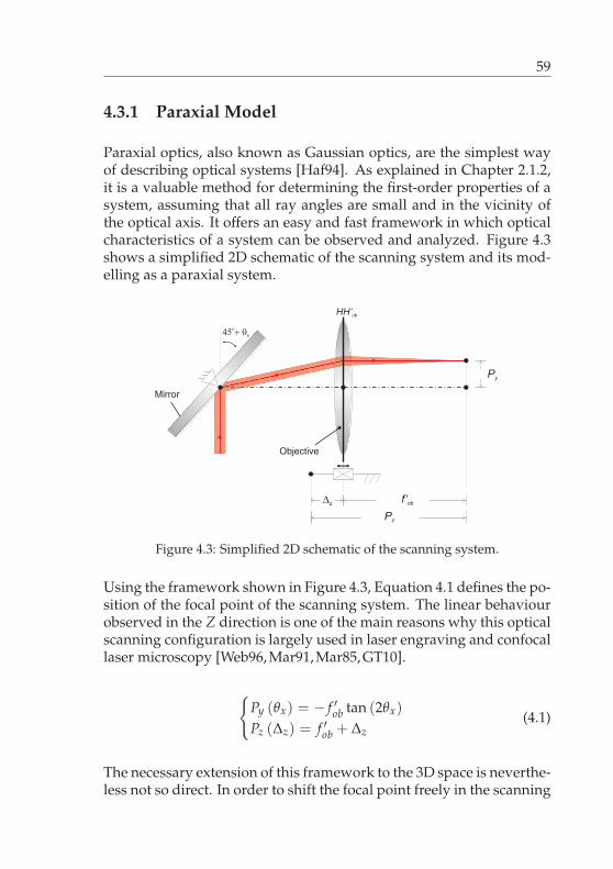
59
4.3.1 Paraxial Model
Paraxial optics, also known as Gaussian optics, are the simplest wayof describing optical systems [Haf94]. As explained in Chapter 2.1.2,it is a valuable method for determining the first-order properties of asystem, assuming that all ray angles are small and in the vicinity ofthe optical axis. It offers an easy and fast framework in which opticalcharacteristics of a system can be observed and analyzed. Figure 4.3shows a simplified 2D schematic of the scanning system and its mod-elling as a paraxial system.
Py
HH’ob
���
x
Mirror
Objective
�z f’ob
Pz
Figure 4.3: Simplified 2D schematic of the scanning system.
Using the framework shown in Figure 4.3, Equation 4.1 defines the po-sition of the focal point of the scanning system. The linear behaviourobserved in the Z direction is one of the main reasons why this opticalscanning configuration is largely used in laser engraving and confocallaser microscopy [Web96, Mar91, Mar85, GT10].
{Py (θx) = − f ′ob tan (2θx)
Pz (Δz) = f ′ob + Δz(4.1)
The necessary extension of this framework to the 3D space is neverthe-less not so direct. In order to shift the focal point freely in the scanning
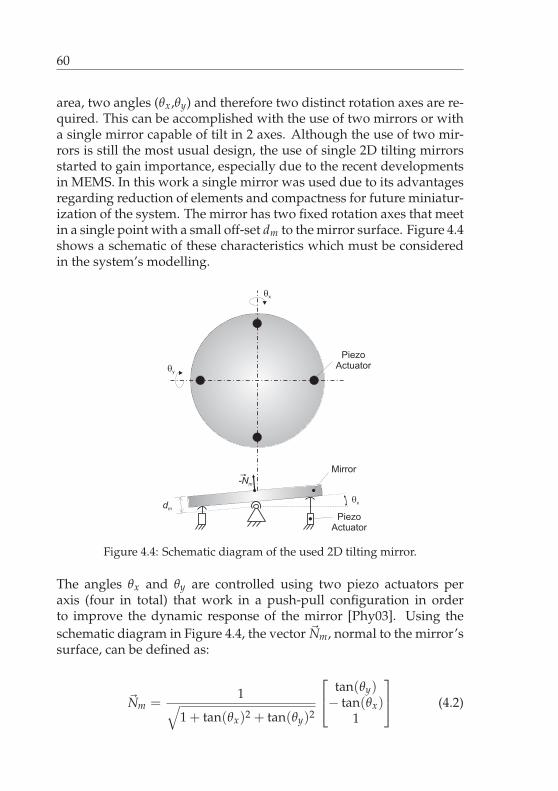
60
area, two angles (θx,θy) and therefore two distinct rotation axes are re-quired. This can be accomplished with the use of two mirrors or witha single mirror capable of tilt in 2 axes. Although the use of two mir-rors is still the most usual design, the use of single 2D tilting mirrorsstarted to gain importance, especially due to the recent developmentsin MEMS. In this work a single mirror was used due to its advantagesregarding reduction of elements and compactness for future miniatur-ization of the system. The mirror has two fixed rotation axes that meetin a single point with a small off-set dm to the mirror surface. Figure 4.4shows a schematic of these characteristics which must be consideredin the system’s modelling.
dm
�x
Mirror
Piezo
Actuator
Piezo
Actuator
�x
�y
-Nm
Figure 4.4: Schematic diagram of the used 2D tilting mirror.
The angles θx and θy are controlled using two piezo actuators peraxis (four in total) that work in a push-pull configuration in orderto improve the dynamic response of the mirror [Phy03]. Using theschematic diagram in Figure 4.4, the vector �Nm, normal to the mirror’ssurface, can be defined as:
�Nm =1√
1 + tan(θx)2 + tan(θy)2
⎡⎣ tan(θy)− tan(θx)
1
⎤⎦ (4.2)
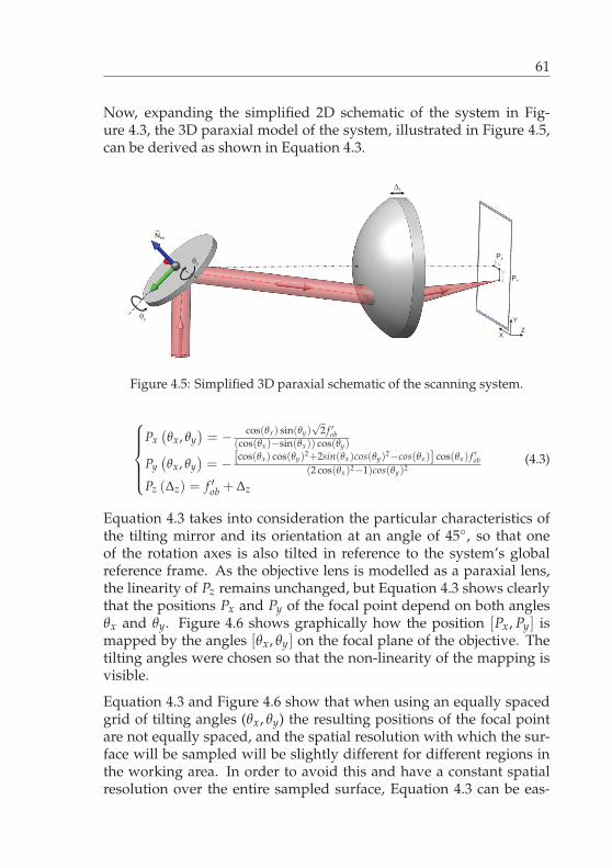
61
Now, expanding the simplified 2D schematic of the system in Fig-ure 4.3, the 3D paraxial model of the system, illustrated in Figure 4.5,can be derived as shown in Equation 4.3.
PX
PY
NMir
X
Y
Z
�z
�x
�y
Figure 4.5: Simplified 3D paraxial schematic of the scanning system.
⎧⎪⎪⎪⎨⎪⎪⎪⎩
Px(θx, θy
)= − cos(θx) sin(θy)
√2 f ′ob
(cos(θx)−sin(θx)) cos(θy)
Py(θx, θy
)= − [cos(θx) cos(θy)2+2sin(θx)cos(θy)2−cos(θx)] cos(θx) f ′ob
(2 cos(θx)2−1)cos(θy)2
Pz (Δz) = f ′ob + Δz
(4.3)
Equation 4.3 takes into consideration the particular characteristics ofthe tilting mirror and its orientation at an angle of 45◦, so that oneof the rotation axes is also tilted in reference to the system’s globalreference frame. As the objective lens is modelled as a paraxial lens,the linearity of Pz remains unchanged, but Equation 4.3 shows clearlythat the positions Px and Py of the focal point depend on both anglesθx and θy. Figure 4.6 shows graphically how the position [Px, Py] ismapped by the angles [θx, θy] on the focal plane of the objective. Thetilting angles were chosen so that the non-linearity of the mapping isvisible.
Equation 4.3 and Figure 4.6 show that when using an equally spacedgrid of tilting angles (θx, θy) the resulting positions of the focal pointare not equally spaced, and the spatial resolution with which the sur-face will be sampled will be slightly different for different regions inthe working area. In order to avoid this and have a constant spatialresolution over the entire sampled surface, Equation 4.3 can be eas-
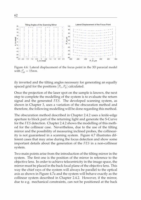
62
Figure 4.6: Lateral displacement of the focus point in the 3D paraxial modelwith f ′ob = 15mm.
ily inverted and the tilting angles necessary for generating an equallyspaced grid for the positions [Px, Py] calculated.
Once the projection of the laser spot on the sample is known, the nextstep to complete the modelling of the system is to evaluate the returnsignal and the generated FES. The developed scanning system, asshown in Chapter 3, uses a variation of the obscuration method andtherefore, the following modelling will be done regarding this method.
The obscuration method described in Chapter 2.4.2 uses a knife-edgeaperture to block part of the returning light and generate the S-Curvefor the FES detection. Chapter 2.4.2 shows the modelling of this meth-od for the collinear case. Nevertheless, due to the use of the tiltingmirror and the possibility of measuring inclined probes, the collinear-ity is not guaranteed in a scanning system. Figure 4.7 illustrates dif-ferent cases that may arise during the focus detection and show someimportant details about the generation of the FES in a non-collinearsystem.
Two main points arise from the introduction of the tilting mirror in thesystem. The first one is the position of the mirror in reference to theobjective lens. In order to achieve telecentricity in the image space, themirror must be placed in the back focal plane of the objective lens. Thisway the chief rays of the system will always be parallel to the opticalaxis as shown in Figure 4.7a and the system will behave exactly as thecollinear system described in Chapter 2.4.2. However, if the mirror,due to e.g. mechanical constraints, can not be positioned at the back
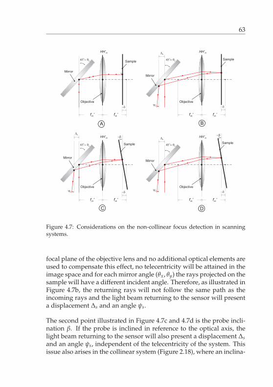
63
HH’ob
���
x
f ’ob
Sample
�s
Mirror
Objective
f ’ob
HH’ob
���
x
f ’ob
Sample
Mirror
Objective
f ’ob
s
�� ��
HH’ob
���
x
f ’ob
Sample
Mirror
Objective
f ’ob
��
���
s
s
HH’ob
���
x
f ’ob
�s
Mirror
Objective
f ’ob
s ��
Sample
��
A B
C D
Figure 4.7: Considerations on the non-collinear focus detection in scanningsystems.
focal plane of the objective lens and no additional optical elements areused to compensate this effect, no telecentricity will be attained in theimage space and for each mirror angle (θx, θy) the rays projected on thesample will have a different incident angle. Therefore, as illustrated inFigure 4.7b, the returning rays will not follow the same path as theincoming rays and the light beam returning to the sensor will presenta displacement Δs and an angle ψs.
The second point illustrated in Figure 4.7c and 4.7d is the probe incli-nation β. If the probe is inclined in reference to the optical axis, thelight beam returning to the sensor will also present a displacement Δsand an angle ψs, independent of the telecentricity of the system. Thisissue also arises in the collinear system (Figure 2.18), where an inclina-
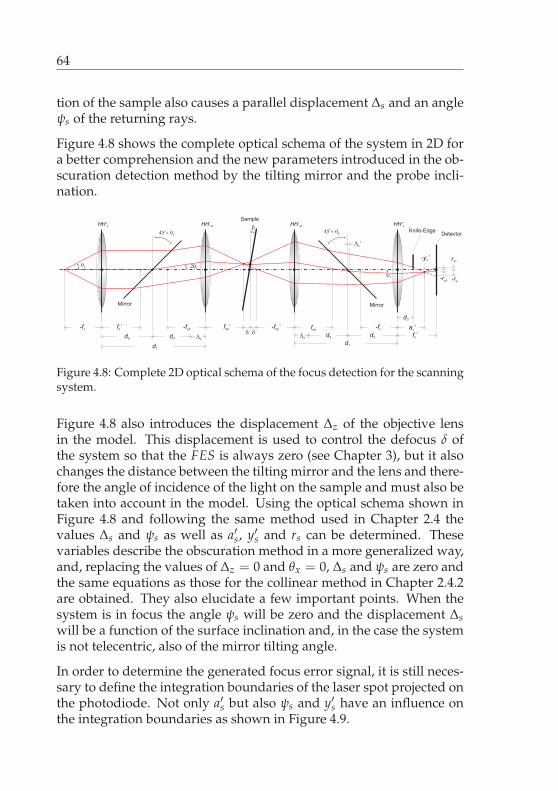
64
tion of the sample also causes a parallel displacement Δs and an angleψs of the returning rays.
Figure 4.8 shows the complete optical schema of the system in 2D fora better comprehension and the new parameters introduced in the ob-scuration detection method by the tilting mirror and the probe incli-nation.
HH’s HH’ob HH’ob HH’s
�-fs f ’s -fob f ’ob -f ’ob
f ’s
fob-fs
�L
Sample
-rs0
a ’s
�
���x
d1
���
x
d1
�
d3
-y ’s
s
d4 �z
d4�z
�’s
��x
rs+
-rs-
Mirror
DetectorKnife-Edge
Mirror
d5d5
Figure 4.8: Complete 2D optical schema of the focus detection for the scanningsystem.
Figure 4.8 also introduces the displacement Δz of the objective lensin the model. This displacement is used to control the defocus δ ofthe system so that the FES is always zero (see Chapter 3), but it alsochanges the distance between the tilting mirror and the lens and there-fore the angle of incidence of the light on the sample and must also betaken into account in the model. Using the optical schema shown inFigure 4.8 and following the same method used in Chapter 2.4 thevalues Δs and ψs as well as a′s, y′s and rs can be determined. Thesevariables describe the obscuration method in a more generalized way,and, replacing the values of Δz = 0 and θx = 0, Δs and ψs are zero andthe same equations as those for the collinear method in Chapter 2.4.2are obtained. They also elucidate a few important points. When thesystem is in focus the angle ψs will be zero and the displacement Δswill be a function of the surface inclination and, in the case the systemis not telecentric, also of the mirror tilting angle.
In order to determine the generated focus error signal, it is still neces-sary to define the integration boundaries of the laser spot projected onthe photodiode. Not only a′s but also ψs and y′s have an influence onthe integration boundaries as shown in Figure 4.9.
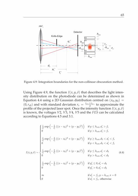
65
HH’s
f ’s
rs+
a ’s
d3
-y ’s
-rs--hcut
hgap
-hmain -rs0
Detector
Knife-Edge
haux
D2
D3
D4
D5
hsize
Figure 4.9: Integration boundaries for the non-collinear obscuration method.
Using Figure 4.9, the function I(x, y, δ) that describes the light inten-sity distribution on the photodiode can be determined as shown inEquation 4.4 using a 2D Gaussian distribution centred on (x0, y0) =
(0, rs0) and with standard deviation rs = rs++rs−2 to approximate the
profile of the projected laser spot. Once the intensity function I(x, y, δ)is known, the voltages V2, V3, V4, V5 and the FES can be calculatedaccording to Equations 4.5 and 3.1.
I(x, y, δ) ∼
⎧⎪⎪⎪⎪⎪⎪⎪⎪⎪⎪⎪⎪⎪⎪⎪⎪⎪⎪⎪⎪⎪⎪⎪⎪⎪⎪⎪⎪⎪⎨⎪⎪⎪⎪⎪⎪⎪⎪⎪⎪⎪⎪⎪⎪⎪⎪⎪⎪⎪⎪⎪⎪⎪⎪⎪⎪⎪⎪⎪⎩
1r2s
exp(− 2
r2s
((x − x0)
2 + (y − y0)2)) if y ≤ hcut, a′s > fs
0 if y > hcut, a′s > fs
1r2s
exp(− 2
r2s
((x − x0)
2 + (y − y0)2)) if y ≥ hcut, d3 < a′s < fs
0 if y < hcut, d3 < a′s < fs
1r2s
exp(− 2
r2s
((x − x0)
2 + (y − y0)2)) if y ≤ hcut, a′s < d3
0 if y > hcut, a′s < d3
1r2s
exp(− 2
r2s
((x − x0)
2 + (y − y0)2)) if y′s ≤ 0, a′s = d3
0 if y′s > 0, a′s = d3
∞ if a′s = fs, y = hcut, x = 00 if a′s = fs, otherwise
(4.4)
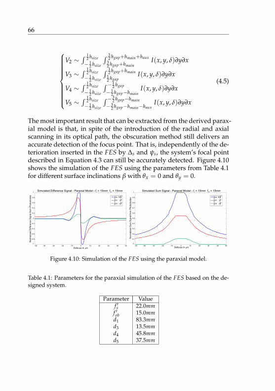
66
V2 ∼∫ 1
2 hsize
− 12 hsize
∫ 32 hgap+hmain+haux
32 hgap+hmain
I(x, y, δ)∂y∂x
V3 ∼∫ 1
2 hsize
− 12 hsize
∫ 12 hgap+hmain
12 hgap
I(x, y, δ)∂y∂x
V4 ∼∫ 1
2 hsize
− 12 hsize
∫ − 12 hgap
− 12 hgap−hmain
I(x, y, δ)∂y∂x
V5 ∼∫ 1
2 hsize
− 12 hsize
∫ − 32 hgap−hmain
− 32 hgap−hmain−haux
I(x, y, δ)∂y∂x
(4.5)
The most important result that can be extracted from the derived parax-ial model is that, in spite of the introduction of the radial and axialscanning in its optical path, the obscuration method still delivers anaccurate detection of the focus point. That is, independently of the de-terioration inserted in the FES by ∆s and ψs, the system’s focal pointdescribed in Equation 4.3 can still be accurately detected. Figure 4.10shows the simulation of the FES using the parameters from Table 4.1for different surface inclinations β with θx = 0 and θy = 0.
ob= +5ob= 0ob= -5
-50 -40 -30 -20 -10 0 10 20 30 40 50
-1
-0.8
-0.6
-0.4
-0.2
0
0.2
0.4
0.6
0.8
1
Defocus in mm
No
rma
lize
d D
iffe
ren
ce S
ign
al f
rom
Ph
oto
dio
de
s
Simulated Difference Signal - Paraxial Model - f = 15mm f = 15mms ob
-50 -40 -30 -20 -10 0 10 20 30 40 50
0
0.1
0.2
0.3
0.4
0.5
0.6
0.7
0.8
0.9
1
Defocus in mm
No
rma
lize
d S
um
Sig
na
l fro
m P
ho
tod
iod
es
Simulated Sum Signal - Paraxial Model - f = 15mm f = 15mms ob
ob= +5ob= 0ob= -5
Figure 4.10: Simulation of the FES using the paraxial model.
Table 4.1: Parameters for the paraxial simulation of the FES based on the de-signed system.
Parameter Valuef ′s 22.0mmf ′ob 15.0mmd1 83.3mmd3 13.5mmd4 45.8mmd5 37.5mm
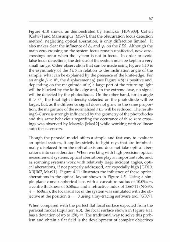
67
Figure 4.10 shows, as demonstrated by Hnilicka [HBVS03], Cohen[Coh87] and Mansuripur [MS97], that the obscuration focus detectionmethod, neglecting optical aberration, is only diffraction limited. Italso makes clear the influence of Δs and ψs on the FES. Although themain zero-crossing on the system focus remain unaffected, new zero-crossings occur when the system is not in focus. In order to avoidfalse focus detections, the defocus of the system must be kept in a verysmall range. Other observation that can be made using Figure 4.10 isthe asymmetry of the FES in relation to the inclination angle of thesample, what can be explained by the presence of the knife-edge. Foran angle β < 0◦, the displacement y′s (see Figure 4.8) is positive and,depending on the magnitude of y′s a large part of the returning lightwill be blocked by the knife-edge and, in the extreme case, no signalwill be detected by the photodiodes. On the other hand, for an angleβ > 0◦, the total light intensity detected on the photodiode will belarger, but, as the difference signal does not grow in the same propor-tion, the magnitude of the normalized FES will be reduced. The result-ing S-Curve is strongly influenced by the geometry of the photodiodesand this same behaviour regarding the occurance of false zero cross-ings was observed by Mastylo [Mas12] while working with collinearauto-focus sensors.
Though the paraxial model offers a simple and fast way to evaluatean optical system, it applies strictly to light rays that are infinitesi-mally displaced from the optical axis and does not take optical aber-rations into consideration. When working with high precision opticalmeasurement systems, optical aberrations play an important role, and,as scanning systems work with relatively large incident angles, opti-cal aberrations, if not properly addressed, are especially high [GD10,XRJR07, Mar91]. Figure 4.11 illustrates the influence of these opticalaberrations in the optical layout shown in Figure 4.5. Using a sim-ple plane-convex spherical lens with a curvature radius of 10.09mm,a centre thickness of 5.50mm and a refractive index of 1.66711 (N-SF5,λ = 650nm), the focal surface of the system was simulated with the ob-jective at the position Δz = 0 using a ray-tracing software tool [GT09].
When compared with the perfect flat focal surface expected from theparaxial model (Equation 4.3), the focal surface shown in Figure 4.11has a deviation of up to 150μm. The traditional way to solve this prob-lem and obtain a flat field is the development of complex objectives
68
Simulated Focal Surface - PCX 15x15
Z in
�m
150
100
50
0
-50
-100
-150
150
100
50
0
-50
-100
-150
200
-200
Y in �m
X in �m
300200
100
0
-100
-200
-300
-400-400
-200-300
-1000
100
200
300
400
Figure 4.11: Influence of optical aberrations using a simple spherical lens ( f =15mm).
that optically compensate these errors and the use of additional opticalcomponents to avoid inconvenient conditions such as the under-fillingof the objective’s entrance pupil [Mar91, Bei95]. As mentioned earlier,this often leads to costly and heavy optics, which reduces system dy-namics and makes measuring times larger. Two different alternativesolutions to address these errors are proposed in this work. Both ofthem act not directly on the optical errors, but on their influence onthe measurements. The first one is based on a more precise model ofthe system using ray-tracing and the second one on the measurementof known artifacts to determine the system’s function experimentally(Chapter 4.4).
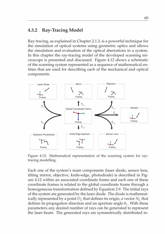
69
4.3.2 Ray-Tracing Model
Ray-tracing, as explained in Chapter 2.1.3, is a powerful technique forthe simulation of optical systems using geometric optics and allowsthe simulation and evaluation of the optical aberrations in a system.In this chapter the ray-tracing model of the developed scanning mi-croscope is presented and discussed. Figure 4.12 shows a schematicof the scanning system represented as a sequence of mathematical en-tities that are used for describing each of the mechanical and opticalcomponents.
Detection Photodiode
Laser Diode Mirror Objective
Sensor LensKnife-Edge Aperture
Global Coordinate Frame
Frame0
Frame1
Frame2
Frame3
Frame6
Frame5
Frame4
T0-1 T
0-3
T0-5
T0-2
T0-6
T0-4
Sample
Frame7
T0-7
Figure 4.12: Mathematical representation of the scanning system for ray-tracing modelling.
Each one of the system’s main components (laser diode, sensor lens,tilting mirror, objective, knife-edge, photodiode) is described in Fig-ure 4.12 within an associated coordinate frame and each one of thesecoordinate frames is related to the global coordinate frame through ahomogeneous transformation defined by Equation 2.9. The initial raysof the system are generated by the laser diode. The diode is mathemat-ically represented by a point OL that defines its origin, a vector NL thatdefines its propagation direction and an aperture angle θL. With theseparameters any desired number of rays can be generated to representthe laser beam. The generated rays are symmetrically distributed in-
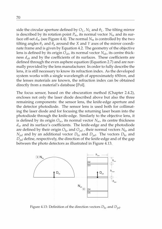
70
side the circular aperture defined by OL, NL and θL. The tilting mirroris described by its rotation point Pm, its normal vector Nm and its sur-face off-set dm (see Figure 4.4). The normal Nm is controlled by the twotilting angles θx and θy around the X and Y axes of the mirror coordi-nate frame and is given by Equation 4.2. The geometry of the objectivelens is defined by its origin Oob, its normal vector Nob, its centre thick-ness dob and by the coefficients of its surfaces. These coefficients aredefined through the even asphere equation (Equation 2.7) and are nor-mally provided by the lens manufacturer. In order to fully describe thelens, it is still necessary to know its refraction index. As the developedsystem works with a single wavelength of approximately 650nm, andthe lenses materials are known, the refraction index can be obtaineddirectly from a material’s database [Pol].
The focus sensor, based on the obscuration method (Chapter 2.4.2),encloses not only the laser diode described above but also the threeremaining components: the sensor lens, the knife-edge aperture andthe detector photodiode. The sensor lens is used both for collimat-ing the laser diode and for focusing the returning laser beam into thephotodiode through the knife-edge. Similarly to the objective lens, itis defined by its origin Ose, its normal vector Nse, its centre thicknessdse and its surface’s coefficients. The knife-edge and the photodiodeare defined by their origin Oke and Opd , their normal vectors Nke andNpd and by an additional vector Dke and Dpd. The vectors Dke andDpd define, respectively, the direction of the knife-edge and of the gapbetween the photo detectors as illustrated in Figure 4.13.
Dke
Dpd
Nke
Npd
hgap
hmain
hauxD2
D3
D4
D5
hsize
Figure 4.13: Definition of the direction vectors Dke and Dpd.
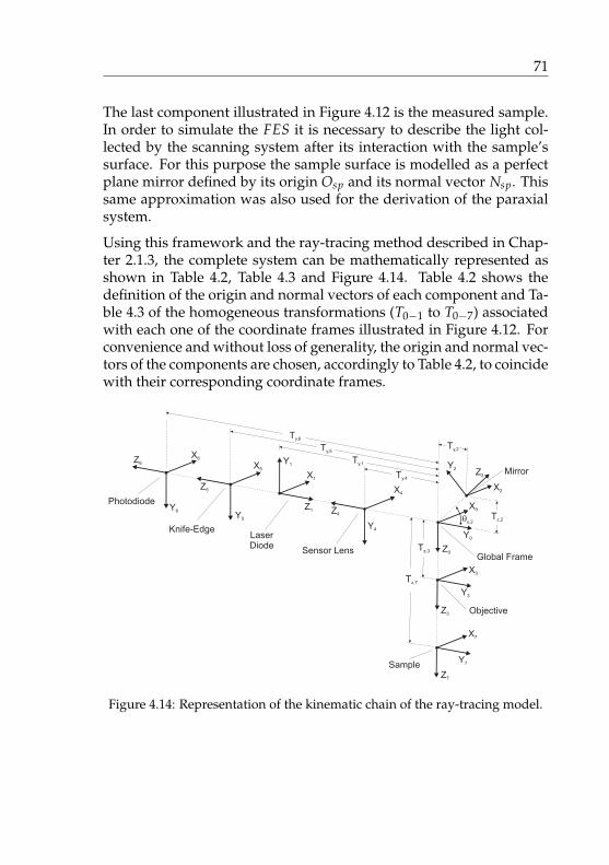
71
The last component illustrated in Figure 4.12 is the measured sample.In order to simulate the FES it is necessary to describe the light col-lected by the scanning system after its interaction with the sample’ssurface. For this purpose the sample surface is modelled as a perfectplane mirror defined by its origin Osp and its normal vector Nsp. Thissame approximation was also used for the derivation of the paraxialsystem.
Using this framework and the ray-tracing method described in Chap-ter 2.1.3, the complete system can be mathematically represented asshown in Table 4.2, Table 4.3 and Figure 4.14. Table 4.2 shows thedefinition of the origin and normal vectors of each component and Ta-ble 4.3 of the homogeneous transformations (T0−1 to T0−7) associatedwith each one of the coordinate frames illustrated in Figure 4.12. Forconvenience and without loss of generality, the origin and normal vec-tors of the components are chosen, accordingly to Table 4.2, to coincidewith their corresponding coordinate frames.
Sample
Sensor Lens
Knife-Edge
Mirror
LaserDiode
Objective
Global Frame
Photodiode
X6
Y6
Z6 X5
Y5
Z5
X1
Y1
Z1
X4
Y4
Z4
X7
Y7
Z7
X3
Y3
Z3
X0
Y0
Z0
X2
Y2Z2
qx,2
Ty,4
Ty,1
Ty,5
Ty,6
Tz,3
Tz,7
Tz,2
Ty,2
Figure 4.14: Representation of the kinematic chain of the ray-tracing model.
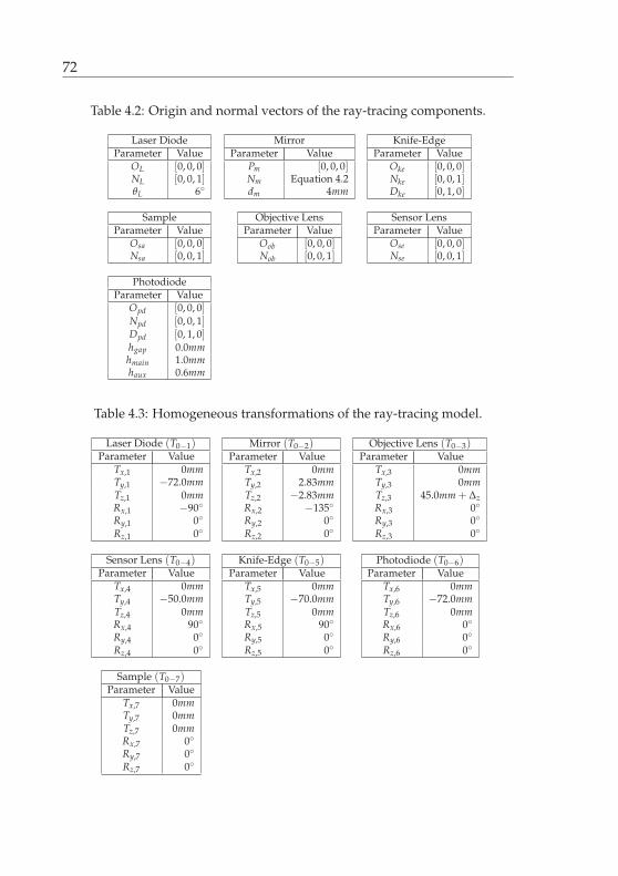
72
Table 4.2: Origin and normal vectors of the ray-tracing components.
Laser DiodeParameter Value
OL [0, 0, 0]NL [0, 0, 1]θL 6◦
MirrorParameter Value
Pm [0, 0, 0]Nm Equation 4.2dm 4mm
Knife-EdgeParameter Value
Oke [0, 0, 0]Nke [0, 0, 1]Dke [0, 1, 0]
SampleParameter Value
Osa [0, 0, 0]Nsa [0, 0, 1]
Objective LensParameter Value
Oob [0, 0, 0]Nob [0, 0, 1]
Sensor LensParameter Value
Ose [0, 0, 0]Nse [0, 0, 1]
PhotodiodeParameter Value
Opd [0, 0, 0]Npd [0, 0, 1]Dpd [0, 1, 0]hgap 0.0mmhmain 1.0mmhaux 0.6mm
Table 4.3: Homogeneous transformations of the ray-tracing model.
Laser Diode (T0−1)Parameter Value
Tx,1 0mmTy,1 −72.0mmTz,1 0mmRx,1 −90◦Ry,1 0◦Rz,1 0◦
Mirror (T0−2)Parameter Value
Tx,2 0mmTy,2 2.83mmTz,2 −2.83mmRx,2 −135◦Ry,2 0◦Rz,2 0◦
Objective Lens (T0−3)Parameter Value
Tx,3 0mmTy,3 0mmTz,3 45.0mm + ΔzRx,3 0◦Ry,3 0◦Rz,3 0◦
Sensor Lens (T0−4)Parameter Value
Tx,4 0mmTy,4 −50.0mmTz,4 0mmRx,4 90◦Ry,4 0◦Rz,4 0◦
Knife-Edge (T0−5)Parameter Value
Tx,5 0mmTy,5 −70.0mmTz,5 0mmRx,5 90◦Ry,5 0◦Rz,5 0◦
Photodiode (T0−6)Parameter Value
Tx,6 0mmTy,6 −72.0mmTz,6 0mmRx,6 0◦Ry,6 0◦Rz,6 0◦
Sample (T0−7)Parameter Value
Tx,7 0mmTy,7 0mmTz,7 0mmRx,7 0◦Ry,7 0◦Rz,7 0◦
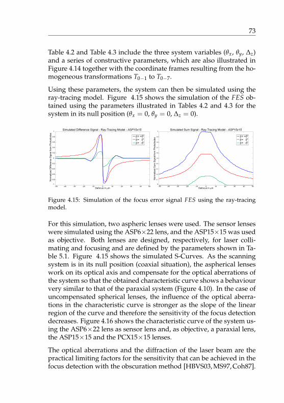
73
Table 4.2 and Table 4.3 include the three system variables (θx, θy, ∆z)and a series of constructive parameters, which are also illustrated inFigure 4.14 together with the coordinate frames resulting from the ho-mogeneous transformations T0−1 to T0−7.
Using these parameters, the system can then be simulated using theray-tracing model. Figure 4.15 shows the simulation of the FES ob-tained using the parameters illustrated in Tables 4.2 and 4.3 for thesystem in its null position (θx = 0, θy = 0, ∆z = 0).
-50 -40 -30 -20 -10 0 10 20 30 40 50
-1
-0.8
-0.6
-0.4
-0.2
0
0.2
0.4
0.6
0.8
1
Defocus in mm
No
rma
lize
d D
iffe
ren
ce S
ign
al f
rom
Ph
oto
dio
de
s
Simulated Difference Signal - Ray-Tracing Model - ASP15x15
-50 -40 -30 -20 -10 0 10 20 30 40 50
0
0.1
0.2
0.3
0.4
0.5
0.6
0.7
0.8
0.9
1
Defocus in mm
No
rma
lize
d S
um
Sig
na
l fro
m P
ho
tod
iod
es
Simulated Sum Signal - Ray-Tracing Model - ASP15x15
ob= +5ob= 0ob= -5
ob= +5ob= 0ob= -5
Figure 4.15: Simulation of the focus error signal FES using the ray-tracingmodel.
For this simulation, two aspheric lenses were used. The sensor lenseswere simulated using the ASP6×22 lens, and the ASP15×15 was usedas objective. Both lenses are designed, respectively, for laser colli-mating and focusing and are defined by the parameters shown in Ta-ble 5.1. Figure 4.15 shows the simulated S-Curves. As the scanningsystem is in its null position (coaxial situation), the aspherical lenseswork on its optical axis and compensate for the optical aberrations ofthe system so that the obtained characteristic curve shows a behaviourvery similar to that of the paraxial system (Figure 4.10). In the case ofuncompensated spherical lenses, the influence of the optical aberra-tions in the characteristic curve is stronger as the slope of the linearregion of the curve and therefore the sensitivity of the focus detectiondecreases. Figure 4.16 shows the characteristic curve of the system us-ing the ASP6×22 lens as sensor lens and, as objective, a paraxial lens,the ASP15×15 and the PCX15×15 lenses.
The optical aberrations and the diffraction of the laser beam are thepractical limiting factors for the sensitivity that can be achieved in thefocus detection with the obscuration method [HBVS03, MS97, Coh87].
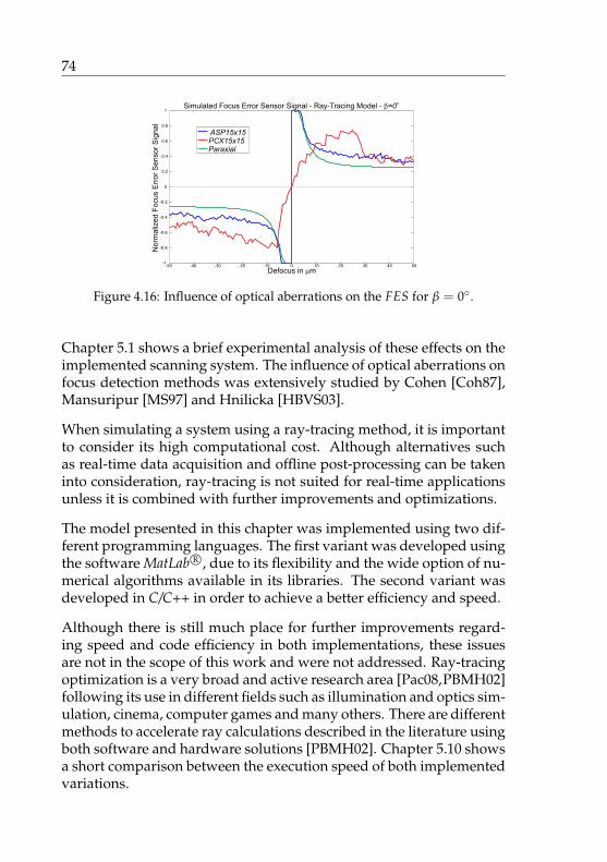
74
-50 -40 -30 -20 -10 0 10 20 30 40 50-1
-0.8
-0.6
-0.4
-0.2
0
0.2
0.4
0.6
0.8
1
Defocus in mm
No
rma
lize
d F
ocu
s E
rro
r S
en
so
r S
ign
al
oSimulated Focus Error Sensor Signal - Ray-Tracing Model - b=0
ASP15x15PCX15x15Paraxial
Figure 4.16: Influence of optical aberrations on the FES for β = 0◦.
Chapter 5.1 shows a brief experimental analysis of these effects on theimplemented scanning system. The influence of optical aberrations onfocus detection methods was extensively studied by Cohen [Coh87],Mansuripur [MS97] and Hnilicka [HBVS03].
When simulating a system using a ray-tracing method, it is importantto consider its high computational cost. Although alternatives suchas real-time data acquisition and offline post-processing can be takeninto consideration, ray-tracing is not suited for real-time applicationsunless it is combined with further improvements and optimizations.
The model presented in this chapter was implemented using two dif-ferent programming languages. The first variant was developed usingthe software MatLab R©, due to its flexibility and the wide option of nu-merical algorithms available in its libraries. The second variant wasdeveloped in C/C++ in order to achieve a better efficiency and speed.
Although there is still much place for further improvements regard-ing speed and code efficiency in both implementations, these issuesare not in the scope of this work and were not addressed. Ray-tracingoptimization is a very broad and active research area [Pac08,PBMH02]following its use in different fields such as illumination and optics sim-ulation, cinema, computer games and many others. There are differentmethods to accelerate ray calculations described in the literature usingboth software and hardware solutions [PBMH02]. Chapter 5.10 showsa short comparison between the execution speed of both implementedvariations.
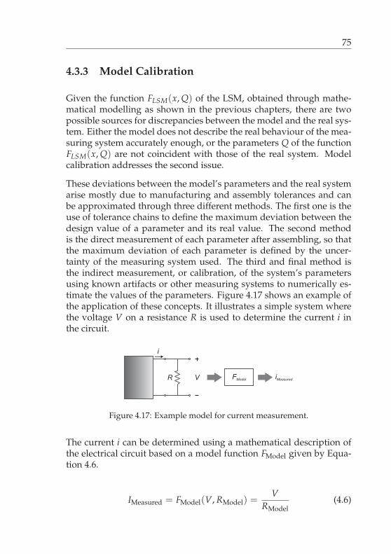
75
4.3.3 Model Calibration
Given the function FLSM(x, Q) of the LSM, obtained through mathe-matical modelling as shown in the previous chapters, there are twopossible sources for discrepancies between the model and the real sys-tem. Either the model does not describe the real behaviour of the mea-suring system accurately enough, or the parameters Q of the functionFLSM(x, Q) are not coincident with those of the real system. Modelcalibration addresses the second issue.
These deviations between the model’s parameters and the real systemarise mostly due to manufacturing and assembly tolerances and canbe approximated through three different methods. The first one is theuse of tolerance chains to define the maximum deviation between thedesign value of a parameter and its real value. The second methodis the direct measurement of each parameter after assembling, so thatthe maximum deviation of each parameter is defined by the uncer-tainty of the measuring system used. The third and final method isthe indirect measurement, or calibration, of the system’s parametersusing known artifacts or other measuring systems to numerically es-timate the values of the parameters. Figure 4.17 shows an example ofthe application of these concepts. It illustrates a simple system wherethe voltage V on a resistance R is used to determine the current i inthe circuit.
VR
i
FModel iMeasured
Figure 4.17: Example model for current measurement.
The current i can be determined using a mathematical description ofthe electrical circuit based on a model function FModel given by Equa-tion 4.6.
IMeasured = FModel(V, RModel) =V
RModel(4.6)
76
The mathematical model FModel has the resistance RModel as its singleparameter. In order for the model to correctly describe the behaviourof the real system and correctly measure the current (i), the value ofRModel must correspond to the real value R of the resistance. Howeverit is not possible to manufacture a resistance with an exact desiredvalue, and the exact real value of the resistance is always unknown, sothat RModel and R will differ from one another by an unknown valueξR given by Equation 4.7.
R = RModel + ξR (4.7)
As explained earlier, there are three different ways of approximatingthe value R, so that the deviation ξR and its influence on the mea-surement are minimized. The first possibility is to use manufactur-ing tolerances. Manufacturing tolerances define with a large mar-gin of confidence the maximum deviation of a given value, so that,the deviation ξR between R and RModel is limited by ±τR and its in-fluence in the measurement can be calculated using error propaga-tion [Kra00, DIN99, JCG08]. In the specific case of the model shownin Equation 4.6, the resultant error in the measurement of the currenti due to manufacturing tolerances is given by the linearization of thefunction FModel using the first order expansion of the Taylor series asshown in Equation 4.8. Using ξR ≤ τR the maximal error can then bedetermined.
ξi ≈√(
∂FModel(V, RModel)
∂RModelξR
)2
=
∣∣∣∣∣ VR2
ModelξR
∣∣∣∣∣ (4.8)
The second possibility is to use a different system to directly measurethe value of R and use the measured value RMeasured as a parameterin the model instead of the design value. This way RModel is nowgiven by RMeasured and the limiting values ±τR of ξR will be definedby the measurement uncertainty of the device used to measure theresistance. This method normally offers a better estimate of the realparameter’s value than the manufacturing tolerances, but is often nota viable alternative due to the number of involved parameters or theimpossibility to perform a direct measurement. The final error in the
77
example function FModel due to the measurement uncertainty will alsogiven by Equation 4.8.
The third and last possibility is the calibration, or indirect measure-ment, of the system’s parameters. It is based on the estimation of themodel’s parameters, the mathematical process of adapting the modelto experimental data. The final parameters are chosen so that the re-sulting output of the model is as close as possible to the observed data.In order to accomplish the estimation, a known input is applied tothe system and its output is measured. With the known input val-ues and the design values of the system’s parameters, the model out-put can also be calculated and the obtained results compared with themeasured ones. Assuming the mathematical model describes the realsystem with enough accuracy, the difference between the values pre-dicted by the model and the actual measured ones can be ascribed tothe parameter deviations in the model and used to indirectly deter-mine these deviations and adapt the model.
In the case of the function FModel, applying n different known currentsi′j, n different voltage values Vj will be acquired by the system illus-trated in Figure 4.17 and used to calculate the values of ij accordingto Equation 4.6. As every measurement has an associated uncertainty,each pair [i′j, ij] yields a different optimal value for RModel. For thissimple example, the value of RModel that best represents the exper-imental data and minimizes ξR can be directly determined throughEquation 4.9 and the limiting values ±τR directly obtained throughthe uncertainties ξi′ and ξV′ associated with the independent variablesi′ and V respectively. The final error in the measurement of the current(i) due to the uncertainty in the calibration of RModel will also be givenby Equation 4.8.
⎧⎪⎨⎪⎩
RModel =1n ∑n
j=1Vji′j
|ξR| ≤ τR ≈√(
ξVi′)2
+(−Vξi′
i′2)2 (4.9)
Due to the complexity of many models it is not always possible toobtain a direct equation to define the deviations of a system’s param-eters as in Equation 4.9. Often the model function itself can not beanalytically defined. In such situations numeric approximation and
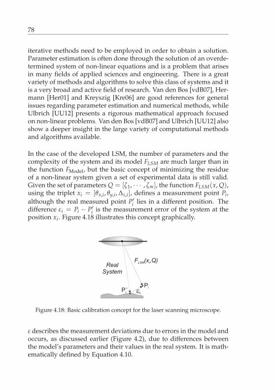
78
iterative methods need to be employed in order to obtain a solution.Parameter estimation is often done through the solution of an overde-termined system of non-linear equations and is a problem that arisesin many fields of applied sciences and engineering. There is a greatvariety of methods and algorithms to solve this class of systems and itis a very broad and active field of research. Van den Bos [vdB07], Her-mann [Her01] and Kreyszig [Kre06] are good references for generalissues regarding parameter estimation and numerical methods, whileUlbrich [UU12] presents a rigorous mathematical approach focusedon non-linear problems. Van den Bos [vdB07] and Ulbrich [UU12] alsoshow a deeper insight in the large variety of computational methodsand algorithms available.
In the case of the developed LSM, the number of parameters and thecomplexity of the system and its model FLSM are much larger than inthe function FModel, but the basic concept of minimizing the residueof a non-linear system given a set of experimental data is still valid.Given the set of parameters Q = [ζ1, · · · , ζm], the function FLSM(x, Q),using the triplet xi = [θx,i, θy,i, Δz,i], defines a measurement point Pi,although the real measured point P′
i lies in a different position. Thedifference εi = Pi − P′
i is the measurement error of the system at theposition xi. Figure 4.18 illustrates this concept graphically.
F (x,Q)LSM iReal
System
Pi
P’i �
i
Figure 4.18: Basic calibration concept for the laser scanning microscope.
ε describes the measurement deviations due to errors in the model andoccurs, as discussed earlier (Figure 4.2), due to differences betweenthe model’s parameters and their values in the real system. It is math-ematically defined by Equation 4.10.
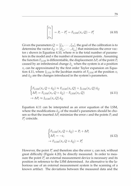
79
⎡⎢⎣
ε1...
εn
⎤⎥⎦ = Pi − P′
i = FLSM(xi, Q)− P′i (4.10)
Given the parameters Q = [ζ1, · · · , ζm], the goal of the calibration is todetermine the vector δQ = [δζ1 , · · · , δζm ] that minimizes the error vec-tor ε shown in Equation 4.10, where m is the total number of parame-ters in the model and n the number of measurement points. Assumingthe function FLSM is differentiable, the displacement ΔPi of the point Picaused by an infinitesimal change δζ j when the system is at a positionxi can be approximated by the first order Taylor expansion on Equa-tion 4.11, where JLSM is the Jacobian matrix of FLSM at the position xiand δQ are the changes introduced in the system’s parameters.
{FLSM(xi, Q + δQ) ≈ FLSM(xi, Q) + JLSM(xi, Q) δQ
ΔPi = FLSM(xi, Q + δQ)− FLSM(xi, Q)
→ ΔPi ≈ JLSM(xi, Q) δQ
(4.11)
Equation 4.11 can be interpreted as an error equation of the LSM,where the modifications δQ of the model’s parameters should be cho-sen so that the inserted ΔPi minimize the error ε and the points Pi andP′
i coincide.
{FLSM(xi, Q + δQ) = Pi + ΔPi
ΔPi = −εi
→ FLSM(xi, Q + δQ) = P′i
(4.12)
However, the point P′i and therefore also the error εi can not, without
great difficulty (Figure 4.20), be directly measured. In order to mea-sure the point P′
i an external measurement device is necessary and itsposition in reference to the LSM determined. An alternative to the la-borious use of an external measurement system is the scanning of aknown artifact. The deviations between the measured data and the
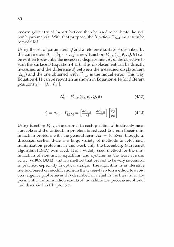
80
known geometry of the artifact can then be used to calibrate the sys-tem’s parameters. With that purpose, the function FLSM must first beremodelled.
Using the set of parameters Q and a reference surface S described bythe parameters B = [b1, · · · , bk] a new function F′
LSM(θx, θy, Q, B) canbe written to describe the necessary displacement Δ′
z of the objective toscan the surface S (Equation 4.13). This displacement can be directlymeasured and the difference ε′i between the measured displacement(Δz,i) and the one obtained with F′
LSM is the model error. This way,Equation 4.11 can be rewritten as shown in Equation 4.14 for differentpositions x′i = [θx,i, θy,i].
Δ′z = F′
LSM(θx, θy, Q, B) (4.13)
ε′i = Δz,i − F′LSM =
[∂F′
LSM∂Q
∂F′LSM∂B
] [δQδB
](4.14)
Using function F′LSM, the error ε′i in each position x′i is directly mea-
sureable and the calibration problem is reduced to a non-linear min-imization problem with the general form Ax = b. Even though, asdiscussed earlier, there is a large variety of methods to solve suchminimization problems, in this work only the Levenberg-Marquardtalgorithm (LMA) was used. It is a widely used method for the min-imization of non-linear equations and systems in the least squaressense [vdB07,UU12] and is a method that proved to be very successfulin practice, especially in optical design. The algorithm is an iterativemethod based on modifications in the Gauss-Newton method to avoidconvergence problems and is described in detail in the literature. Ex-perimental and simulation results of the calibration process are shownand discussed in Chapter 5.3.
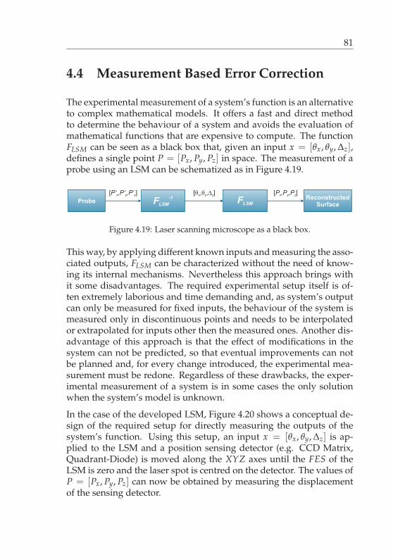
81
4.4 Measurement Based Error Correction
The experimental measurement of a system’s function is an alternativeto complex mathematical models. It offers a fast and direct methodto determine the behaviour of a system and avoids the evaluation ofmathematical functions that are expensive to compute. The functionFLSM can be seen as a black box that, given an input x = [θx, θy, Δz],defines a single point P = [Px, Py, Pz] in space. The measurement of aprobe using an LSM can be schematized as in Figure 4.19.
[�,�,�]x y z
[P’ ,P’ ,P’ ]x y z-1
FLSMProbe FLSM
ReconstructedSurface
[P ,P ,P ]x y z
Figure 4.19: Laser scanning microscope as a black box.
This way, by applying different known inputs and measuring the asso-ciated outputs, FLSM can be characterized without the need of know-ing its internal mechanisms. Nevertheless this approach brings withit some disadvantages. The required experimental setup itself is of-ten extremely laborious and time demanding and, as system’s outputcan only be measured for fixed inputs, the behaviour of the system ismeasured only in discontinuous points and needs to be interpolatedor extrapolated for inputs other then the measured ones. Another dis-advantage of this approach is that the effect of modifications in thesystem can not be predicted, so that eventual improvements can notbe planned and, for every change introduced, the experimental mea-surement must be redone. Regardless of these drawbacks, the exper-imental measurement of a system is in some cases the only solutionwhen the system’s model is unknown.
In the case of the developed LSM, Figure 4.20 shows a conceptual de-sign of the required setup for directly measuring the outputs of thesystem’s function. Using this setup, an input x = [θx, θy, Δz] is ap-plied to the LSM and a position sensing detector (e.g. CCD Matrix,Quadrant-Diode) is moved along the XYZ axes until the FES of theLSM is zero and the laser spot is centred on the detector. The values ofP = [Px, Py, Pz] can now be obtained by measuring the displacementof the sensing detector.
82
LSM
SensingElement
MovableTable
Length MeasurementSystem
Y
X
Z
Figure 4.20: Conceptual design for the direct measurement of FLSM.
Although the measurement rig in Figure 4.20 illustrates the basic con-cept for the direct measurement of the function of the LSM, it is arather complex setup. In order to facilitate this experimental measure-ment, an alternative approach was used. The measurement task wasdivided into two stages. Firstly a flat mirror (λ/20) was positionedperpendicular to the scanning microscope and moved in the Z direc-tion as shown in Figure 4.21. Choosing a single point in the work area(e.g. (θx, θy) = (0, 0)), the position of the mirror in Z0,0 can be deter-mined directly from Δz and the mirror mathematically described asZ = Z0,0. Repeating this process for diferent Z positions, a series ofmeasuring points with the form (θx, θy, Δz) → Pz can be acquired.
Scanning
System
Flat Mirror
Linear
Stage
Figure 4.21: Conceptual design for the direct measurement of FLSM.
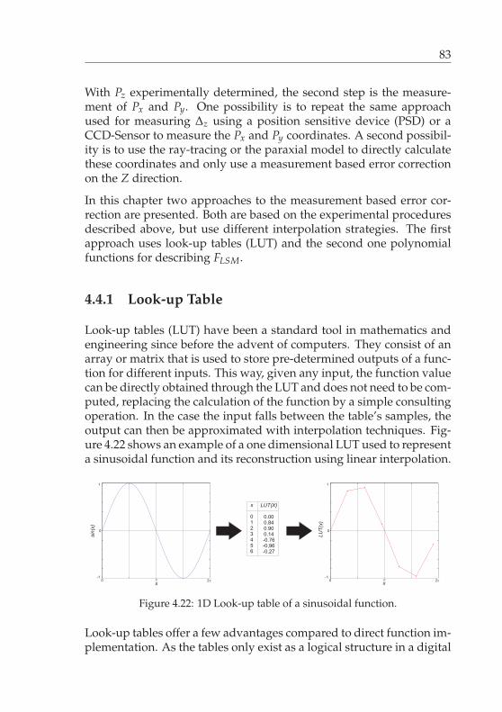
83
With Pz experimentally determined, the second step is the measure-ment of Px and Py. One possibility is to repeat the same approachused for measuring Δz using a position sensitive device (PSD) or aCCD-Sensor to measure the Px and Py coordinates. A second possibil-ity is to use the ray-tracing or the paraxial model to directly calculatethese coordinates and only use a measurement based error correctionon the Z direction.
In this chapter two approaches to the measurement based error cor-rection are presented. Both are based on the experimental proceduresdescribed above, but use different interpolation strategies. The firstapproach uses look-up tables (LUT) and the second one polynomialfunctions for describing FLSM.
4.4.1 Look-up Table
Look-up tables (LUT) have been a standard tool in mathematics andengineering since before the advent of computers. They consist of anarray or matrix that is used to store pre-determined outputs of a func-tion for different inputs. This way, given any input, the function valuecan be directly obtained through the LUT and does not need to be com-puted, replacing the calculation of the function by a simple consultingoperation. In the case the input falls between the table’s samples, theoutput can then be approximated with interpolation techniques. Fig-ure 4.22 shows an example of a one dimensional LUT used to representa sinusoidal function and its reconstruction using linear interpolation.
0-1
0
1
2��x
sin
(x)
0-1
0
1
2��x
LU
T(x
)
x
0
1
2
3
4
5
6
LUT(X)
0.00
0.84
0.90
0.14
-0.76
-0,96
-0.27
Figure 4.22: 1D Look-up table of a sinusoidal function.
Look-up tables offer a few advantages compared to direct function im-plementation. As the tables only exist as a logical structure in a digital
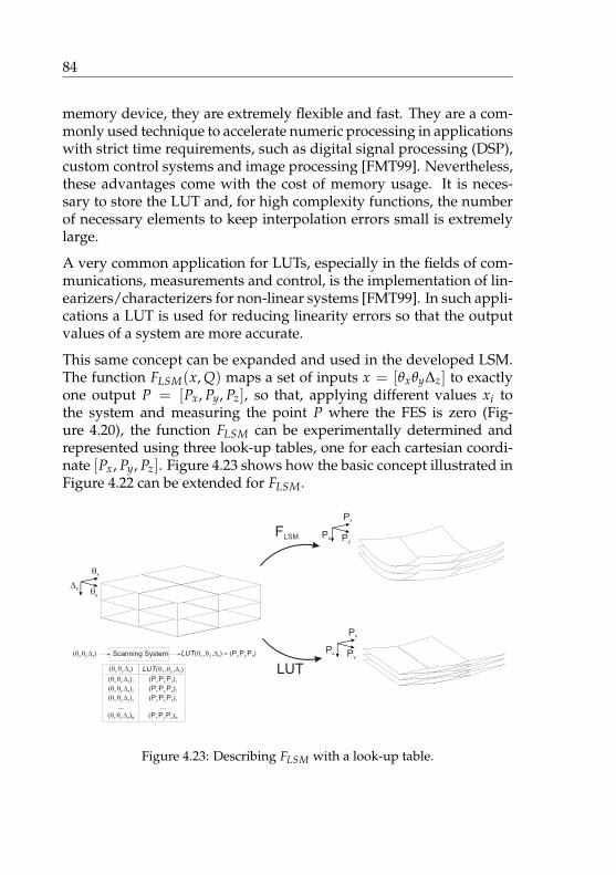
84
memory device, they are extremely flexible and fast. They are a com-monly used technique to accelerate numeric processing in applicationswith strict time requirements, such as digital signal processing (DSP),custom control systems and image processing [FMT99]. Nevertheless,these advantages come with the cost of memory usage. It is neces-sary to store the LUT and, for high complexity functions, the numberof necessary elements to keep interpolation errors small is extremelylarge.
A very common application for LUTs, especially in the fields of com-munications, measurements and control, is the implementation of lin-earizers/characterizers for non-linear systems [FMT99]. In such appli-cations a LUT is used for reducing linearity errors so that the outputvalues of a system are more accurate.
This same concept can be expanded and used in the developed LSM.The function FLSM(x, Q) maps a set of inputs x = [θxθy∆z] to exactlyone output P = [Px, Py, Pz], so that, applying different values xi tothe system and measuring the point P where the FES is zero (Fig-ure 4.20), the function FLSM can be experimentally determined andrepresented using three look-up tables, one for each cartesian coordi-nate [Px, Py, Pz]. Figure 4.23 shows how the basic concept illustrated inFigure 4.22 can be extended for FLSM.
qx
Dz qy
Px
Pz Py
Px
Pz Py
FLSM
LUTLUT(q ,q ,D )x y z
(q q D )x y z 1
(q q D )x y z 2
(q q D )x y z 3
...(q q D )x y z N
Scanning System
(q q D )x y z
(P P P )x y z 1
(P P P )x y z 2
(P P P )x y z 3
...(P P P )x y z N
(q q D )x y z LUT(q ,q ,D ) = (P P P )x y z x y z
Figure 4.23: Describing FLSM with a look-up table.
85
Another possibility, to avoid the necessity a complex measurement rigas shown in Figure 4.20, is to use the paraxial or the ray-tracing modelfor representing the Px and Py coordinates and use a single LUT tocorrect the errors on Pz.
4.4.2 Polynomials
Look-up tables (LUT) are not the only method to approximate mul-tivariate functions. There are numerous methods for approximatingsuch functions and the use of polynomials is one of the most classi-cal ones. Polynomials are a very simple and well known group ofmathematical functions. They are extremely easy to evaluate and aretherefore widely used in many fields, including the interpolation andapproximation of functions. They are well described in the literatureand authors such as Phillips [Phi03] and Hermann [Her01] give a thor-oughly and comprehensive description of the development of polyno-mials and the theory behind polynomial approximations and their usein numerical mathematics.
Polynomials are an extremely convenient way of approximating func-tions. They can not only be easily differentiated and integrated, re-sulting in another polynomial, but they can also approximate con-tinuous functions with any desired accuracy. The Weierstrass theo-rem [Her01, Phi03] states that, for any continuous function F(x) on aclosed interval J = [a, b], there is a polynomial pn(x) such that Equa-tion 4.15 is valid for any chosen error ε > 0.
|F(x)− p(x)| < ε, x ∈ J (4.15)
A polynomial can be generally described as shown in Equation 4.16,where pn(x) is a so called basis function.
p(x) = c0 + c1 p1(x) + c2 p2(x) + · · ·+ cn pn(x) (4.16)
Many different types of polynomials can be obtained by choosing dif-ferent basis functions pn(x). Nevertheless, for convenience, the basisfunction is often chosen as a polynomial itself [Phi03]. There is a widevariety of polynomials that can be chosen as basis for representing a
86
polynomial approximation. The Lagrange-Polynomials, the Newton-Polynomials and the Chebyshev-Polynomials are just a few examples.Each one of these basis polynomials have its own characteristics andare well documented in the literature [Phi03,Her01] especially for uni-variate interpolation.
In the case of multivariate interpolation, although approximation tech-niques are still not well developed, they are still a powerful mathe-matical tool. With that in mind and in order to overcome some ofthe drawbacks of LUTs, a polynomial approach was also implementedfor approximating the function of the developed scanning microscope.The implemented approximation method is described in this chapterbased on the more rigorous approach to the general problem of multi-variate polynomial approximations given by Phillips [Phi03].
It can be shown that, given a positive integer n and a set of pointsSn defined by Equation 4.17 where every xi, yj and zk are distinct,then there is a unique polynomial p(x, y, z), with degree n, given byEquation 4.18 that takes the same values as a function f (x, y, z) on theset Sn.
Sn ={(xi, yj, zk) | i, j, k > 0, i + j + k ≤ n
}(4.17)
p(x, y, z) =n
∑i=0
(n−i)
∑j=0
(n−i−j)
∑k=0
ci,j,kxiyjzk (4.18)
The reason behind Sn is to define a minimal data set to guarantee thatthe polynomial coefficients ci,j,k can be uniquely determined though alinear system of equations as illustrated in Equation 4.19 for the casen = 2.
For representing the function FLSM using this approach, one differentpolynomial is necessary for representing each of the cartesian coordi-nates of the system’s focus point. Another possibility, as mentionedin Chapter 4.4.1, is to use the paraxial or the ray-tracing model forrepresenting the Px and Py coordinates and use a single polynomialto correct the system errors only on Pz. Although this approach doesnot take in account the errors in X and Y it has the advantage that acomplex measurement rig as shown in Figure 4.20 is not necessary. In

87
this work the paraxial approach was used. The obtained results arepresented and discussed in Chapter 5.
⎡⎢⎢⎢⎢⎢⎢⎢⎢⎢⎢⎢⎢⎢⎣
c0,0,0c1,0,0c0,1,0c0,0,1c2,0,0c1,1,0c1,0,1c0,2,0c0,1,1c0,0,2
⎤⎥⎥⎥⎥⎥⎥⎥⎥⎥⎥⎥⎥⎥⎦
10×1
= A−1
⎡⎢⎢⎢⎢⎢⎢⎢⎢⎢⎢⎢⎢⎢⎣
f (x0, y0, z0)f (x1, y0, z0)f (x0, y1, z0)f (x0, y0, z1)f (x2, y0, z0)f (x1, y1, z0)f (x1, y0, z1)f (x0, y2, z0)f (x0, y1, z1)f (x0, y0, z2)
⎤⎥⎥⎥⎥⎥⎥⎥⎥⎥⎥⎥⎥⎥⎦
10×1
| (xi , yj, zk) ∈ Sn (4.19)
A =
⎡⎢⎢⎢⎢⎢⎢⎢⎢⎢⎢⎢⎢⎢⎢⎣
1 x0 y0 z0 x20 x0y0 x0z0 y2
0 y0z0 z20
1 x0 y0 z1 x20 x0y0 x0z1 y2
0 y0z1 z21
1 x0 y0 z2 x20 x0y0 x0z2 y2
0 y0z2 z22
1 x0 y1 z0 x20 x0y1 x0z0 y2
1 y1z0 z20
1 x0 y1 z1 x20 x0y1 x0z1 y2
1 y1z1 z21
1 x0 y2 z0 x20 x0y2 x0z0 y2
2 y2z0 z20
1 x1 y0 z0 x21 x1y0 x1z0 y2
0 y0z0 z20
1 x1 y0 z1 x21 x1y0 x1z1 y2
0 y0z1 z21
1 x1 y1 z0 x21 x1y1 x1z0 y2
1 y1z0 z20
1 x2 y0 z0 x22 x2y0 x2z0 y2
0 y0z0 z20
⎤⎥⎥⎥⎥⎥⎥⎥⎥⎥⎥⎥⎥⎥⎥⎦
10×10
| (xi , yj, zk) ∈ Sn
(4.20)

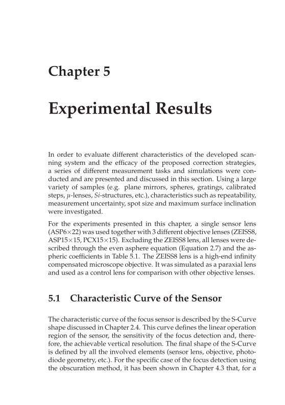
Chapter 5
Experimental Results
In order to evaluate different characteristics of the developed scan-ning system and the efficacy of the proposed correction strategies,a series of different measurement tasks and simulations were con-ducted and are presented and discussed in this section. Using a largevariety of samples (e.g. plane mirrors, spheres, gratings, calibratedsteps, μ-lenses, Si-structures, etc.), characteristics such as repeatability,measurement uncertainty, spot size and maximum surface inclinationwere investigated.
For the experiments presented in this chapter, a single sensor lens(ASP6×22) was used together with 3 different objective lenses (ZEISS8,ASP15×15, PCX15×15). Excluding the ZEISS8 lens, all lenses were de-scribed through the even asphere equation (Equation 2.7) and the as-pheric coefficients in Table 5.1. The ZEISS8 lens is a high-end infinitycompensated microscope objective. It was simulated as a paraxial lensand used as a control lens for comparison with other objective lenses.
5.1 Characteristic Curve of the Sensor
The characteristic curve of the focus sensor is described by the S-Curveshape discussed in Chapter 2.4. This curve defines the linear operationregion of the sensor, the sensitivity of the focus detection and, there-fore, the achievable vertical resolution. The final shape of the S-Curveis defined by all the involved elements (sensor lens, objective, photo-diode geometry, etc.). For the specific case of the focus detection usingthe obscuration method, it has been shown in Chapter 4.3 that, for a
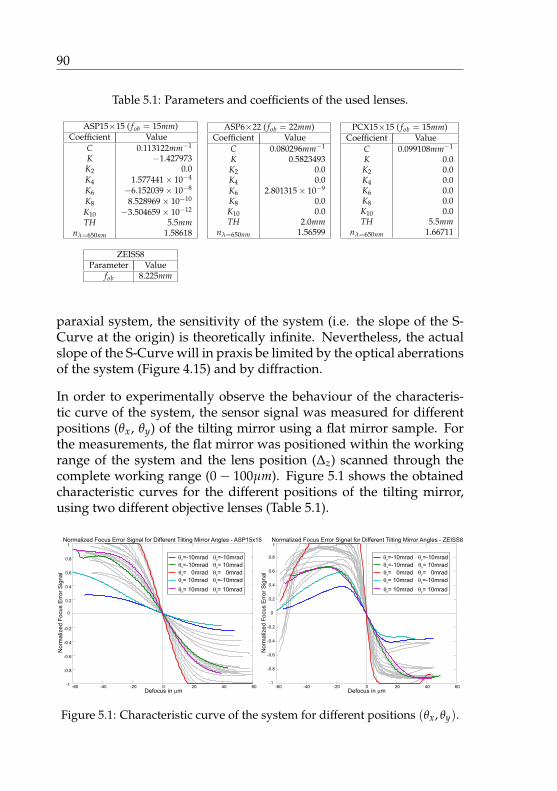
90
Table 5.1: Parameters and coefficients of the used lenses.
ASP15×15 ( fob = 15mm)Coefficient Value
C 0.113122mm−1
K −1.427973K2 0.0K4 1.577441× 10⁻⁴
K6 −6.152039× 10⁻⁸
K8 8.528969× 10⁻¹⁰
K10 −3.504659× 10⁻¹²
TH 5.5mmnλ=650nm 1.58618
ASP6×22 ( fob = 22mm)Coefficient Value
C 0.080296mm−1
K 0.5823493K2 0.0K4 0.0K6 2.801315× 10⁻⁹
K8 0.0K10 0.0TH 2.0mm
nλ=650nm 1.56599
PCX15×15 ( fob = 15mm)Coefficient Value
C 0.099108mm−1
K 0.0K2 0.0K4 0.0K6 0.0K8 0.0K10 0.0TH 5.5mm
nλ=650nm 1.66711
ZEISS8Parameter Value
fob 8.225mm
paraxial system, the sensitivity of the system (i.e. the slope of the S-Curve at the origin) is theoretically infinite. Nevertheless, the actualslope of the S-Curve will in praxis be limited by the optical aberrationsof the system (Figure 4.15) and by diffraction.
In order to experimentally observe the behaviour of the characteris-tic curve of the system, the sensor signal was measured for differentpositions (θx, θy) of the tilting mirror using a flat mirror sample. Forthe measurements, the flat mirror was positioned within the workingrange of the system and the lens position (∆z) scanned through thecomplete working range (0− 100µm). Figure 5.1 shows the obtainedcharacteristic curves for the different positions of the tilting mirror,using two different objective lenses (Table 5.1).
-60 -40 -20 0 20 40 60-1
-0.8
-0.6
-0.4
-0.2
0
0.2
0.4
0.6
0.8
1
Defocus in mm
Norm
aliz
ed F
ocu
s E
rror
Sig
nal
Normalized Focus Error Signal for Different Tilting Mirror Angles - ASP15x15
q =-10mrad q = 10mrad x y
q = 0mrad q = 0mrad x y
q = 10mrad q =-10mrad x y
q = 10mrad q = 10mrad x y
q =-10mrad q =-10mrad x y
-60 -40 -20 0 20 40 60-1
-0.8
-0.6
-0.4
-0.2
0
0.2
0.4
0.6
0.8
1
Defocus in mm
Norm
aliz
ed F
ocu
s E
rror
Sig
nal
Normalized Focus Error Signal for Different Tilting Mirror Angles - ZEISS8
q =-10mrad q = 10mrad x y
q = 0mrad q = 0mrad x y
q = 10mrad q =-10mrad x y
q = 10mrad q = 10mrad x y
q =-10mrad q =-10mrad x y
Figure 5.1: Characteristic curve of the system for different positions (θx, θy).
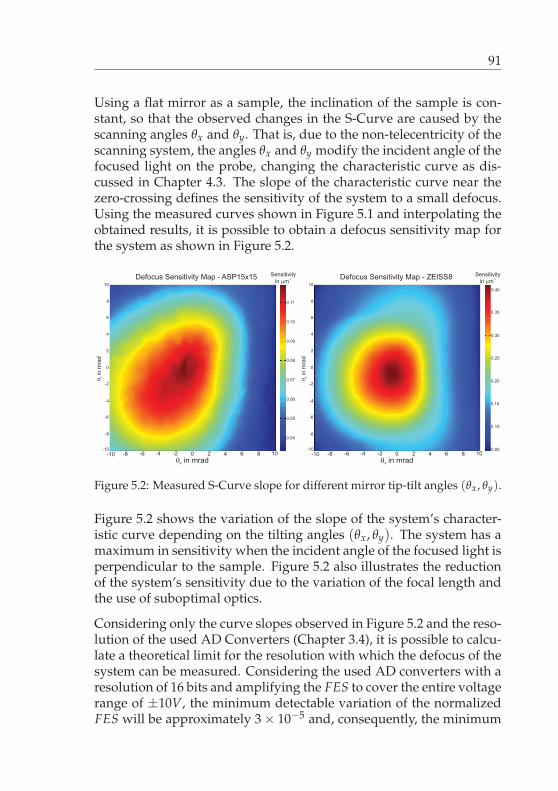
91
Using a flat mirror as a sample, the inclination of the sample is con-stant, so that the observed changes in the S-Curve are caused by thescanning angles θx and θy. That is, due to the non-telecentricity of thescanning system, the angles θx and θy modify the incident angle of thefocused light on the probe, changing the characteristic curve as dis-cussed in Chapter 4.3. The slope of the characteristic curve near thezero-crossing defines the sensitivity of the system to a small defocus.Using the measured curves shown in Figure 5.1 and interpolating theobtained results, it is possible to obtain a defocus sensitivity map forthe system as shown in Figure 5.2.
Defocus Sensitivity Map - ASP15x15
� in mradx
� in m
rad
y
Sensitivity-1
in �m
-10 -8 -6 -4 0 2 4 6 8-10
-8
-6
-4
0
-2
2
4
6
8
10
0.04
0.06
0.08
0.10
0.09
0.07
0.11
0.05
-2 10
Defocus Sensitivity Map - ZEISS8
� in mradx
� in m
rad
y
Sensitivity-1
in �m
-10 -8 -6 -4 0 2 4 6 8-10
-8
-6
-4
0
-2
2
4
6
8
10
0.10
0.25
0.40
0.15
0.35
-2 10
0.30
0.20
0.05
Figure 5.2: Measured S-Curve slope for different mirror tip-tilt angles (θx, θy).
Figure 5.2 shows the variation of the slope of the system’s character-istic curve depending on the tilting angles (θx, θy). The system has amaximum in sensitivity when the incident angle of the focused light isperpendicular to the sample. Figure 5.2 also illustrates the reductionof the system’s sensitivity due to the variation of the focal length andthe use of suboptimal optics.
Considering only the curve slopes observed in Figure 5.2 and the reso-lution of the used AD Converters (Chapter 3.4), it is possible to calcu-late a theoretical limit for the resolution with which the defocus of thesystem can be measured. Considering the used AD converters with aresolution of 16 bits and amplifying the FES to cover the entire voltagerange of ±10V, the minimum detectable variation of the normalizedFES will be approximately 3 × 10⁻⁵ and, consequently, the minimum
92
detectable defocus will vary from 0.3nm to 1nm for the ASP15×15lens and from 0.1nm to 0.3nm for the high-end microscope objective(ZEISS8).
5.2 Error and Sensitivity Analysis
An instrument is defined through its structure and its interaction withthe environment and it will always perform its task with an associ-ated inaccuracy [Kra00]. This inaccuracy depends on a series of fac-tors such as the instrument’s working principle, manufacturing andassembling. Even though it can be minimized, as shown in Chap-ter 4.2, this associated inaccuracy will always be present. In Chapter 4the developed laser scanning microscope was described as a math-ematical function FLSM(x, Q), where Q represents the parameters ofthe system and fully describes its structure and functionality. In thissection, the implemented ray-tracing model is used to evaluate theinfluence of each parameter in the error behaviour of the developedscanning microscope.
However, before describing the error behaviour of the system, it iswise to introduce two important related concepts and their definitions:invariance, and innocence [Sch82, Kra00]. Both concepts are widelyused in mechanical and optical design in order to minimize the influ-ence of manufacturing and assembling deviations as well as environ-mental variations in the output of a system. Equation 5.1 illustratesthese concepts mathematically.
ΔΩ = V1ΔΥ + V2(ΔΥ)2 + · · ·+ Vn(ΔΥ)
n
{V1 = V2 = · · · = Vn = 0 → InvarianceV1 = 0 → Innocence
(5.1)
A system is invariant or innocent according to its error coefficientsV1 · · ·Vn. It is invariant if its output Ω is not influenced by a distur-bance ΔΥ of a parameter Υ, and it is innocent if a disturbance causesonly second or higher order errors. The error coefficients Vn can bedetermined through the Taylor series accordingly to Equation 5.2.
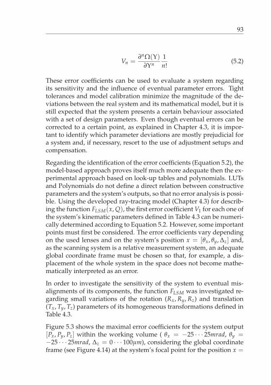
93
Vn =∂nΩ(Υ)
∂Υn1n!
(5.2)
These error coefficients can be used to evaluate a system regardingits sensitivity and the influence of eventual parameter errors. Tighttolerances and model calibration minimize the magnitude of the de-viations between the real system and its mathematical model, but it isstill expected that the system presents a certain behaviour associatedwith a set of design parameters. Even though eventual errors can becorrected to a certain point, as explained in Chapter 4.3, it is impor-tant to identify which parameter deviations are mostly prejudicial fora system and, if necessary, resort to the use of adjustment setups andcompensation.
Regarding the identification of the error coefficients (Equation 5.2), themodel-based approach proves itself much more adequate then the ex-perimental approach based on look-up tables and polynomials. LUTsand Polynomials do not define a direct relation between constructiveparameters and the system’s outputs, so that no error analysis is possi-ble. Using the developed ray-tracing model (Chapter 4.3) for describ-ing the function FLSM(x, Q), the first error coefficient V1 for each one ofthe system’s kinematic parameters defined in Table 4.3 can be numeri-cally determined according to Equation 5.2. However, some importantpoints must first be considered. The error coefficients vary dependingon the used lenses and on the system’s position x = [θx, θy, Δz] and,as the scanning system is a relative measurement system, an adequateglobal coordinate frame must be chosen so that, for example, a dis-placement of the whole system in the space does not become mathe-matically interpreted as an error.
In order to investigate the sensitivity of the system to eventual mis-alignments of its components, the function FLSM was investigated re-garding small variations of the rotation (Rx, Ry, Rz) and translation(Tx, Ty, Tz) parameters of its homogeneous transformations defined inTable 4.3.
Figure 5.3 shows the maximal error coefficients for the system output[Px, Py, Pz] within the working volume ( θx = −25 · · · 25mrad, θy =−25 · · · 25mrad, Δz = 0 · · · 100μm), considering the global coordinateframe (see Figure 4.14) at the system’s focal point for the position x =
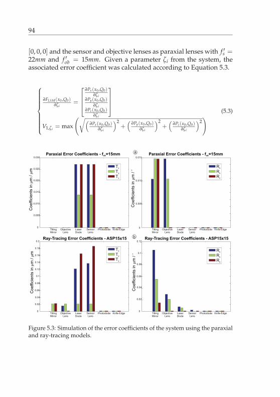
94
[0, 0, 0] and the sensor and objective lenses as paraxial lenses with f ′s =22mm and f ′ob = 15mm. Given a parameter ζi from the system, theassociated error coefficient was calculated according to Equation 5.3.
⎧⎪⎪⎪⎪⎪⎪⎪⎨⎪⎪⎪⎪⎪⎪⎪⎩
∂FLSM(x0,Q0)∂ζi
=
⎡⎢⎢⎣
∂Px(x0,Q0)∂ζi
∂Py(x0,Q0)∂ζi
∂Pz(x0,Q0)∂ζi
⎤⎥⎥⎦
V1,ζi = max
(√(∂Px(x0,Q0)
∂ζi
)2+(
∂Py(x0,Q0)∂ζi
)2+(
∂Pz(x0,Q0)∂ζi
)2) (5.3)
Figure 5.3: Simulation of the error coefficients of the system using the paraxialand ray-tracing models.
95
The error coefficients of the paraxial system shown in Figure 5.3a il-lustrate the robustness of the system. Considering only the positionof its components, the system is innocent regarding small displace-ments of all components with exception to the displacement of thesensor lens and the photodiode; that is, the distance between photo-diode and sensor lens. By changing this distance, the collimation ofthe laser is strongly influenced, causing not only a displacement of theentire focal plane of the system, but also inserting a curvature, influ-encing the X, Y and Z positions of the detected focus point. Regardingthe orientation of its components, although not innocent, the systemdemonstrates a highly insensitive behaviour. The angle of incidenceof the laser on the objective lens has a strong influence on the X and Ypositions of the focus point.
Figure 5.3b shows the error coefficients obtained using the same simu-lation procedures when the lenses are not considered paraxial. Usingthe ray-tracing model and the ASP15×15 and ASP6×22 as objectivelens and sensor lens respectively, the influence of the optical aberra-tions in the error coefficients can be observed. Not only is the systemmore sensitive to eventual misalignments, but also loses its innocenceregarding various parameters.
The error coefficients of the system are important for the numericalidentification of the system’s model. They define which parametersshould be calibrated and which ones can not be calibrated. Chapter 5.3shows the results of the system’s calibration.
96
5.3 Model Calibration and Function
Measurement
As explained in Chapter 4.3.3, the calibration of the system’s modelconsists of the identification of its functional parameters based on mea-sured data. This way, the discrepancies between the model and thereal system caused by manufacturing and assembly tolerances are min-imized.
The first step in order to calibrate the system’s model FLSM is to definewhich parameters are to be identified. The following two character-istics are the most important when using kinematic chains to mathe-matically describe a system: continuity and minimality [GM11]. Theydirectly influence the parameter identification process and are relatedto model smoothness and to parameter redundancies in the model.Mathematically, model continuity is equivalent to continuity of the in-verse function of the model (FLSM
−1). This way, parameterizaton’ssingularity can be defined as a rank deficiency in the jacobian matrix(Equation 4.11) and each parameterization can be investigated con-cerning its singularities through the detection of the zeros of the de-terminant det(JLSM
T JLSM).
To avoid singularities and numerical instability in the calibration pro-cess, not all parameters should be identified, or, in other words, invari-ant parameters should not be included in the identification process.Repeating the error analysis shown in Chapter 5.2 for the functionF′
LSM, Table 5.2 shows the parameters included in the identificationprocess and their values before and after the calibration procedure.The tilting mirror was chosen as reference for defining the global co-ordinate frame.
The identification of the system’s parameters is done using a highquality (λ/20) flat mirror as a reference artifact and considering it asa perfect plane. After measuring the flat mirror, its surface is recon-structed using the ray-tracing model and the acquired data (θx, θy, Δz).Comparing the obtained surface with an ideal geometric plane, all de-viation can be interpreted as model errors and the system’s param-eters modified as shown in Chapter 4.3.3 in order to minimize thesedeviations.
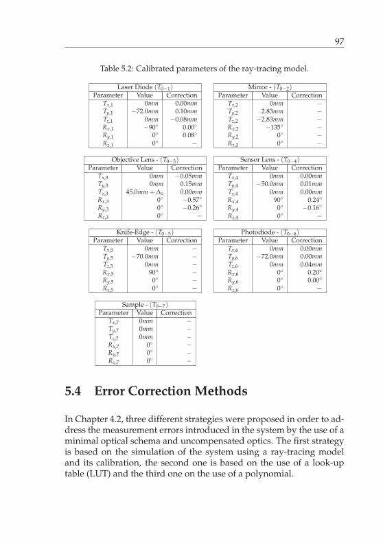
97
Table 5.2: Calibrated parameters of the ray-tracing model.
Laser Diode (T0−1)Parameter Value Correction
Tx,1 0mm 0.00mmTy,1 −72.0mm 0.10mmTz,1 0mm −0.08mmRx,1 −90◦ 0.00◦Ry,1 0◦ 0.08◦Rz,1 0◦ −
Mirror - (T0−2)Parameter Value Correction
Tx,2 0mm −Ty,2 2.83mm −Tz,2 −2.83mm −Rx,2 −135◦ −Ry,2 0◦ −Rz,2 0◦ −
Objective Lens - (T0−3)Parameter Value Correction
Tx,3 0mm −0.05mmTy,3 0mm 0.15mmTz,3 45.0mm + Δz 0.00mmRx,3 0◦ −0.57◦Ry,3 0◦ −0.26◦Rz,3 0◦ −
Sensor Lens - (T0−4)Parameter Value Correction
Tx,4 0mm 0.00mmTy,4 −50.0mm 0.01mmTz,4 0mm 0.00mmRx,4 90◦ 0.24◦Ry,4 0◦ −0.16◦Rz,4 0◦ −
Knife-Edge - (T0−5)Parameter Value Correction
Tx,5 0mm −Ty,5 −70.0mm −Tz,5 0mm −Rx,5 90◦ −Ry,5 0◦ −Rz,5 0◦ −
Photodiode - (T0−6)Parameter Value Correction
Tx,6 0mm 0.00mmTy,6 −72.0mm 0.00mmTz,6 0mm 0.04mmRx,6 0◦ 0.20◦Ry,6 0◦ 0.00◦Rz,6 0◦ −
Sample - (T0−7)Parameter Value Correction
Tx,7 0mm −Ty,7 0mm −Tz,7 0mm −Rx,7 0◦ −Ry,7 0◦ −Rz,7 0◦ −
5.4 Error Correction Methods
In Chapter 4.2, three different strategies were proposed in order to ad-dress the measurement errors introduced in the system by the use of aminimal optical schema and uncompensated optics. The first strategyis based on the simulation of the system using a ray-tracing modeland its calibration, the second one is based on the use of a look-uptable (LUT) and the third one on the use of a polynomial.
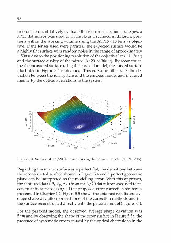
98
In order to quantitatively evaluate these error correction strategies, aλ/20 flat mirror was used as a sample and scanned in different posi-tions within the working volume using the ASP15×15 lens as objec-tive. If the lenses used were paraxial, the expected surface would bea highly flat surface with random noise in the range of approximately±50nm due to the positioning resolution of the objective lens (±13nm)and the surface quality of the mirror (λ/20 ≈ 30nm). By reconstruct-ing the measured surface using the paraxial model, the curved surfaceillustrated in Figure 5.4 is obtained. This curvature illustrates the de-viation between the real system and the paraxial model and is causedmainly by the optical aberrations in the system.
Y in �m
X in �m
Z in �
m
10
5
0
-5
-10
300
200
100
0
-100
-200
-300
20
15
300
200
100
0
-100
-200
-300
0
5
10
-5
-10
15
Z in
�m
Figure 5.4: Surface of a λ/20 flat mirror using the paraxial model (ASP15×15).
Regarding the mirror surface as a perfect flat, the deviations betweenthe reconstructed surface shown in Figure 5.4 and a perfect geometricplane can be interpreted as the modelling error. With this approach,the captured data ([θx, θy, Δz]) from the λ/20 flat mirror was used to re-construct its surface using all the proposed error correction strategiespresented in Chapter 4.2. Figure 5.5 shows the obtained results and av-erage shape deviation for each one of the correction methods and forthe surface reconstructed directly with the paraxial model (Figure 5.4).
For the paraxial model, the observed average shape deviation was5μm and by observing the shape of the error surface in Figure 5.5a, thepresence of systematic errors caused by the optical aberrations in the
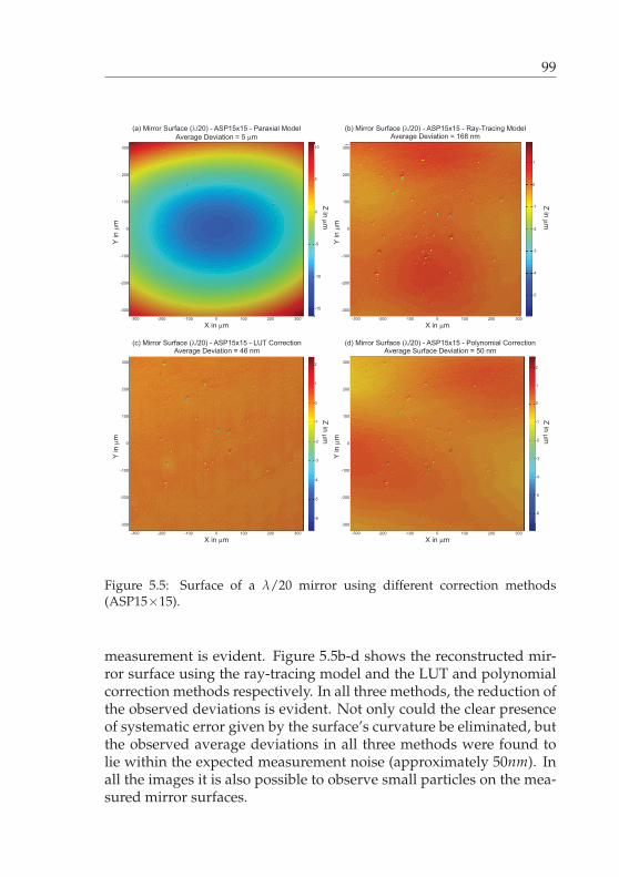
99
X in �m
Y in
�m
-200 -100 0 200
-200
0
-100
100
200
300
-2
0
-1
1
100
Z in
�m
(c) Mirror Surface (�/20) - ASP15x15 - LUT Correction
Average Deviation = 46 nm
-300
-3
-4
-300
300
-5
-6
2
X in �m
Y in
�m
-200 -100 0 200
-200
0
-100
100
200
300
0
5
100
Z in
�m
(a) Mirror Surface (�/20) - ASP15x15 - Paraxial Model
Average Deviation = 5 �m
-300
-5
-300
300
-10
-15
10
X in �m
Y in
�m
-200 -100 0 200
-200
0
-100
100
200
300
-2
0
100
Z in
�m
(b) Mirror Surface (�/20) - ASP15x15 - Ray-Tracing Model
Average Deviation = 168 nm
-300
-3
-300
300
-4
1
X in �m
Y in
�m
-200 -100 0 200
-200
0
-100
100
200
300
-2
0
-1
1
100
Z in
�m
(d) Mirror Surface (�/20) - ASP15x15 - Polynomial Correction
Average Surface Deviation = 50 nm
-300
-3
-4
-300
300
-5
-6
2
-1
-5
Figure 5.5: Surface of a λ/20 mirror using different correction methods(ASP15×15).
measurement is evident. Figure 5.5b-d shows the reconstructed mir-ror surface using the ray-tracing model and the LUT and polynomialcorrection methods respectively. In all three methods, the reduction ofthe observed deviations is evident. Not only could the clear presenceof systematic error given by the surface’s curvature be eliminated, butthe observed average deviations in all three methods were found tolie within the expected measurement noise (approximately 50nm). Inall the images it is also possible to observe small particles on the mea-sured mirror surfaces.
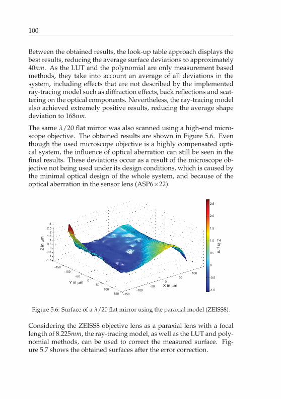
100
Between the obtained results, the look-up table approach displays thebest results, reducing the average surface deviations to approximately40nm. As the LUT and the polynomial are only measurement basedmethods, they take into account an average of all deviations in thesystem, including effects that are not described by the implementedray-tracing model such as diffraction effects, back reflections and scat-tering on the optical components. Nevertheless, the ray-tracing modelalso achieved extremely positive results, reducing the average shapedeviation to 168nm.
The same λ/20 flat mirror was also scanned using a high-end micro-scope objective. The obtained results are shown in Figure 5.6. Eventhough the used microscope objective is a highly compensated opti-cal system, the influence of optical aberration can still be seen in thefinal results. These deviations occur as a result of the microscope ob-jective not being used under its design conditions, which is caused bythe minimal optical design of the whole system, and because of theoptical aberration in the sensor lens (ASP6×22).
Y in �mX in �m
Z in �
m
1
2.5
0
1.5
-1
150
100
50
0
-50
-100
-150
3
2
-150
-100
-50
0
50
100
1.0
1.5
2.0
0.5
0
2.5
0.5
-0.5
-1.5
-0.5
-1.0
Z in
�m
Figure 5.6: Surface of a λ/20 flat mirror using the paraxial model (ZEISS8).
Considering the ZEISS8 objective lens as a paraxial lens with a focallength of 8.225mm, the ray-tracing model, as well as the LUT and poly-nomial methods, can be used to correct the measured surface. Fig-ure 5.7 shows the obtained surfaces after the error correction.
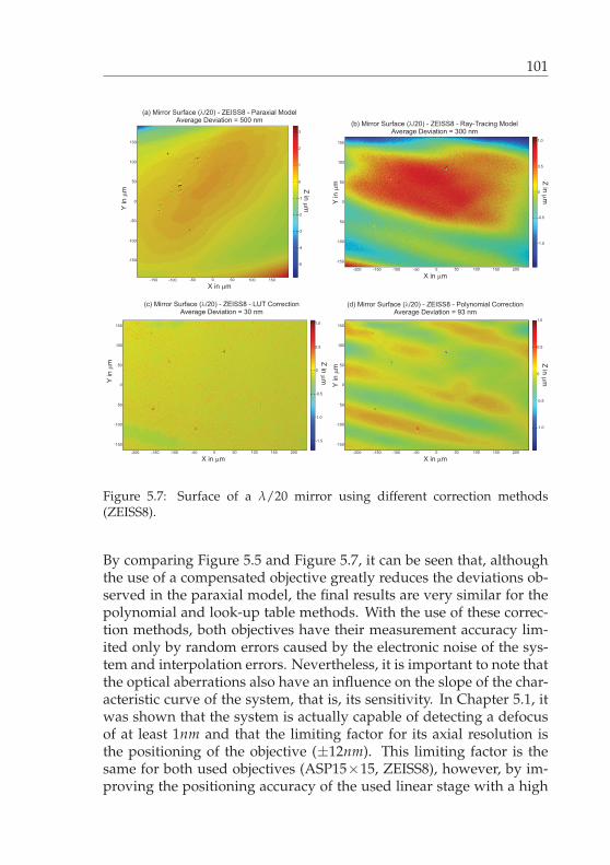
101
X in �m
Y in
�m
-150 -100 500
-150
100
-100
50
0
150
-0.5
0.5
0
1.0
-50
Z in
�m
-200
-1.0
X in �m
Y in
�m
-100 -50 1000
-150
100
-100
50
0
150
0
2
1
3
50
Z in
�m
-150
-1
-5
-50
150
-4
-3
-2
(a) Mirror Surface (�/20) - ZEISS8 - Paraxial Model
Average Deviation = 500 nm(b) Mirror Surface (�/20) - ZEISS8 -
Average Deviation = 300 nm
Ray-Tracing Model
(d) Mirror Surface (�/20) - ZEISS8 -
Average Deviation = 93 nm
Polynomial Correction(c) Mirror Surface (�/20) - ZEISS8 -
Average Deviation = 30 nm
LUT Correction
50
100 200150
X in �m
Y in
�m
-150 -100 500
-150
100
-100
50
0
150
-0.5
0.5
0
1.0
-50
Z in
�m
-200
-1.0
50
100 200150
Z in
�m
Z in
�m
X in �m
Y in
�m
-150 -100 500
-150
100
-100
50
0
150
-0.5
0.5
0
1.0
-50
Z in
�m
-200
-1.0
50
100 200150
-1.5
Figure 5.7: Surface of a λ/20 mirror using different correction methods(ZEISS8).
By comparing Figure 5.5 and Figure 5.7, it can be seen that, althoughthe use of a compensated objective greatly reduces the deviations ob-served in the paraxial model, the final results are very similar for thepolynomial and look-up table methods. With the use of these correc-tion methods, both objectives have their measurement accuracy lim-ited only by random errors caused by the electronic noise of the sys-tem and interpolation errors. Nevertheless, it is important to note thatthe optical aberrations also have an influence on the slope of the char-acteristic curve of the system, that is, its sensitivity. In Chapter 5.1, itwas shown that the system is actually capable of detecting a defocusof at least 1nm and that the limiting factor for its axial resolution isthe positioning of the objective (±12nm). This limiting factor is thesame for both used objectives (ASP15×15, ZEISS8), however, by im-proving the positioning accuracy of the used linear stage with a high
102
resolution DA converter, the limiting factor of the achievable resolu-tion would be the system’s sensitivity. In this case, the quality of thecompensated objective could be truly utilized.
It is important to note that the use of non-model-based correction meth-ods such as LUTs or polynomials also leads to a growth of the mea-surement uncertainty of the system. The numerical correction func-tions are constructed through the measurement of an artifact and havewithin them an associated measurement uncertainty given by the re-petability of the system and the surface quality of the used artifact.When reconstructing a surface using one of these methods, the finalmeasurement uncertainty will be given by the addition of the uncer-tainty of the numerical function and of the actual measurement.
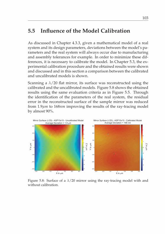
103
5.5 Influence of the Model Calibration
As discussed in Chapter 4.3.3, given a mathematical model of a realsystem and its design parameters, deviations between the model’s pa-rameters and the real system will always occur due to manufacturingand assembly tolerances for example. In order to minimize these dif-ferences, it is necessary to calibrate the model. In Chapter 5.3, the ex-perimental calibration procedure and the obtained results were shownand discussed and in this section a comparison between the calibratedand uncalibrated models is shown.
Scanning a λ/20 flat mirror, its surface was reconstructed using thecalibrated and the uncalibrated models. Figure 5.8 shows the obtainedresults using the same evaluation criteria as in Figure 5.5. Throughthe identification of the parameters of the real system, the residualerror in the reconstructed surface of the sample mirror was reducedfrom 1.9μm to 168nm improving the results of the ray-tracing modelby almost 90%.
Mirror Surface (�/20)
Average Deviation = 168 nm
- ASP15x15 - Calibrated Model
X in �m
Y in
�m
-200 -100 200 300
-300
-100
-200
100
200
300
0
2
1
3
100
Z in
�m
Mirror Surface (�/20) - ASP15x15 - Uncalibrated Model
Average Deviation = 1.9 �m
-300
-4
-5
0
0
-3
-2
-1
4
5
X in �m
Y in
�m
-200 -100 200 300
-300
-100
-200
100
200
300
-1
-2
0
100
Z in
�m
-300
0
0
-5
-4
-3
1
Figure 5.8: Surface of a λ/20 mirror using the ray-tracing model with andwithout calibration.
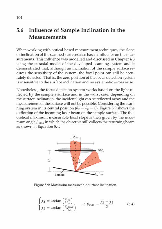
104
5.6 Influence of Sample Inclination in the
Measurements
When working with optical-based measurement techniques, the slopeor inclination of the scanned surfaces also has an influence on the mea-surements. This influence was modelled and discussed in Chapter 4.3using the paraxial model of the developed scanning system and itdemonstrated that, although an inclination of the sample surface re-duces the sensitivity of the system, the focal point can still be accu-rately detected. That is, the zero position of the focus detection systemis insensitive to the surface inclination and no systematic errors arise.
Nonetheless, the focus detection system works based on the light re-flected by the sample’s surface and in the worst case, depending onthe surface inclination, the incident light can be reflected away and themeasurement of the surface will not be possible. Considering the scan-ning system in its central position (θx = θy = 0), Figure 5.9 shows thedeflection of the incoming laser beam on the sample surface. The the-oretical maximum measurable local slope is then given by the maxi-mum angle βmax in which the objective still collects the returning beamas shown in Equation 5.4.
HH’ob
f ’ob
Sample�
max
Laser
ob
�1
�2
Figure 5.9: Maximum measureable surface inclination.
⎧⎨⎩
χ1 = arctan(�ob
2 fob
)χ2 = arctan
(�Laser2 fob
) → βmax =χ1 + χ2
2(5.4)
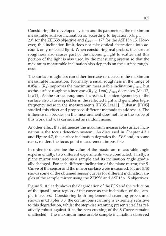
105
Considering the developed system and its parameters, the maximummeasurable surface inclination is, according to Equation 5.4, βmax =23◦ for the ZEISS8 objective and βmax = 17◦ for the ASP15×15. How-ever, this inclination limit does not take optical aberrations into ac-count, only reflected light. When considering real probes, the surfaceroughness also causes part of the incoming light to scatter and thisportion of the light is also used by the measuring system so that themaximum measurable inclination also depends on the surface rough-ness.
The surface roughness can either increase or decrease the maximummeasurable inclination. Normally, a small roughness in the range of0.05μm (Ra) improves the maximum measurable inclination βmax, butas the surface roughness increases (Ra ≥ 1μm), βmax decreases [Mas12,Lea11]. As the surface roughness increases, the micro-geometry of thesurface also causes speckles in the reflected light and generates high-frequency noise in the measurements [FY05, Lea11]. Fukatsu [FY05]studied this effect and proposed different methods to address it. Theinfluence of speckles on the measurement does not lie in the scope ofthis work and was considered as random noise.
Another effect that influences the maximum measurable surface incli-nation is the focus detection system. As discussed in Chapter 4.3.1and Figure 4.7, the surface inclination degrades the FES and, in somecases, renders the focus point measurement impossible.
In order to determine the value of the maximum measurable angleexperimentally, two different experiments were conducted. Firstly, aplane mirror was used as a sample and its inclination angle gradu-ally changed. For each different inclination of the plane mirror, the S-Curve of the sensor and the mirror surface were measured. Figure 5.10shows some of the obtained sensor curves for different inclination an-gles of the sample mirror using the ZEISS8 and ASP15×15 objectives.
Figure 5.10 clearly shows the degradation of the FES and the reductionof the quasi-linear region of the curve as the inclination of the sam-ple increases. Considering both implemented scanning proceduresshown in Chapter 3.3, the continuous scanning is extremely sensitiveto this degradation, whilst the stepwise scanning presents itself as rel-atively robust against it as the zero-crossing of the S-Curve remainsunaffected. The maximum measurable sample inclination observed
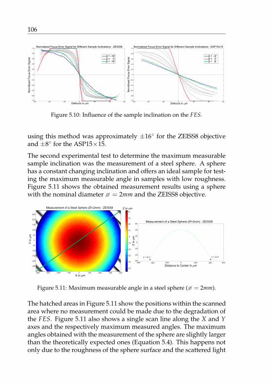
106
-60 -40 -20 0 20 40 60-1.0
-0.8
-0.6
-0.4
-0.2
0
0.2
0.4
0.6
0.8
1.0
Defocus in mm
No
rmili
zed
Fo
cus E
rro
r S
ign
al
Normalized Focus Error Signal for Different Sample Inclinations - ZEISS8
β o = -16β o = 0β
o = 16
-60 -40 -20 0 20 40 60-1.0
-0.8
-0.6
-0.4
-0.2
0
0.2
0.4
0.6
0.8
1.0
Defocus in mm
No
rmili
zed
Fo
cus
Err
or
Sig
na
l
Normalized Focus Error Signal for Different Sample Inclinations - ASP15x15
β o = - 8β o = 0β
o = 8
Figure 5.10: Influence of the sample inclination on the FES.
using this method was approximately ±16◦ for the ZEISS8 objectiveand ±8◦ for the ASP15×15.
The second experimental test to determine the maximum measurablesample inclination was the measurement of a steel sphere. A spherehas a constant changing inclination and offers an ideal sample for test-ing the maximum measurable angle in samples with low roughness.Figure 5.11 shows the obtained measurement results using a spherewith the nominal diameter � = 2mm and the ZEISS8 objective.
Measurement of a Steel Sphere (O=2mm) - ZEISS8
X in mm
Y in
mm
Z in mm
-400 -300 -200 -100 0 100 200 300 400
-250
-200
-150
-100
0
-50
50
100
150
200
250
Z in
mm
Distance to Center in mm-400-600 -200 0 200 600400
ob = 25.5o
b = 24.9
Measurement of a Steel Sphere (O=2mm) - ZEISS8
-60
-40
-20
0
20
40
60
-40
-20
0
20
40
10
-10
30
-30
-50
Figure 5.11: Maximum measurable angle in a steel sphere (� = 2mm).
The hatched areas in Figure 5.11 show the positions within the scannedarea where no measurement could be made due to the degradation ofthe FES. Figure 5.11 also shows a single scan line along the X and Yaxes and the respectively maximum measured angles. The maximumangles obtained with the measurement of the sphere are slightly largerthan the theoretically expected ones (Equation 5.4). This happens notonly due to the roughness of the sphere surface and the scattered light
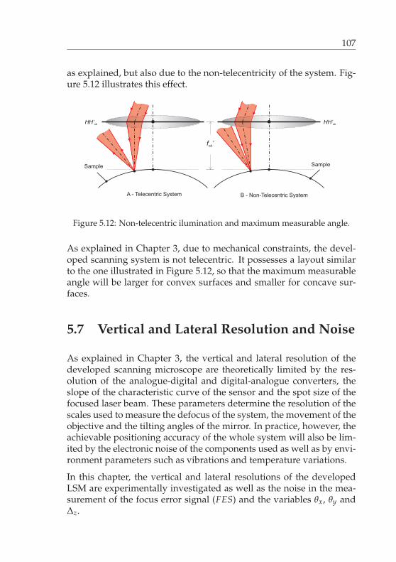
107
as explained, but also due to the non-telecentricity of the system. Fig-ure 5.12 illustrates this effect.
HH’ob
Sample
f ’ob
Sample
HH’ob
A - Telecentric System B - Non-Telecentric System
Figure 5.12: Non-telecentric ilumination and maximum measurable angle.
As explained in Chapter 3, due to mechanical constraints, the devel-oped scanning system is not telecentric. It possesses a layout similarto the one illustrated in Figure 5.12, so that the maximum measurableangle will be larger for convex surfaces and smaller for concave sur-faces.
5.7 Vertical and Lateral Resolution and Noise
As explained in Chapter 3, the vertical and lateral resolution of thedeveloped scanning microscope are theoretically limited by the res-olution of the analogue-digital and digital-analogue converters, theslope of the characteristic curve of the sensor and the spot size of thefocused laser beam. These parameters determine the resolution of thescales used to measure the defocus of the system, the movement of theobjective and the tilting angles of the mirror. In practice, however, theachievable positioning accuracy of the whole system will also be lim-ited by the electronic noise of the components used as well as by envi-ronment parameters such as vibrations and temperature variations.
In this chapter, the vertical and lateral resolutions of the developedLSM are experimentally investigated as well as the noise in the mea-surement of the focus error signal (FES) and the variables θx, θy andΔz.
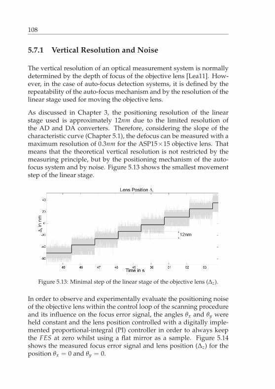
108
5.7.1 Vertical Resolution and Noise
The vertical resolution of an optical measurement system is normallydetermined by the depth of focus of the objective lens [Lea11]. How-ever, in the case of auto-focus detection systems, it is defined by therepeatability of the auto-focus mechanism and by the resolution of thelinear stage used for moving the objective lens.
As discussed in Chapter 3, the positioning resolution of the linearstage used is approximately 12nm due to the limited resolution ofthe AD and DA converters. Therefore, considering the slope of thecharacteristic curve (Chapter 5.1), the defocus can be measured with amaximum resolution of 0.3nm for the ASP15×15 objective lens. Thatmeans that the theoretical vertical resolution is not restricted by themeasuring principle, but by the positioning mechanism of the auto-focus system and by noise. Figure 5.13 shows the smallest movementstep of the linear stage.
Figure 5.13: Minimal step of the linear stage of the objective lens (Δz).
In order to observe and experimentally evaluate the positioning noiseof the objective lens within the control loop of the scanning procedureand its influence on the focus error signal, the angles θx and θy wereheld constant and the lens position controlled with a digitally imple-mented proportional-integral (PI) controller in order to always keepthe FES at zero whilst using a flat mirror as a sample. Figure 5.14shows the measured focus error signal and lens position (Δz) for theposition θx = 0 and θy = 0.
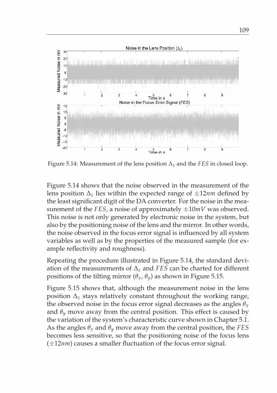
109
Figure 5.14: Measurement of the lens position Δz and the FES in closed loop.
Figure 5.14 shows that the noise observed in the measurement of thelens position Δz lies within the expected range of ±12nm defined bythe least significant digit of the DA converter. For the noise in the mea-surement of the FES, a noise of approximately ±10mV was observed.This noise is not only generated by electronic noise in the system, butalso by the positioning noise of the lens and the mirror. In other words,the noise observed in the focus error signal is influenced by all systemvariables as well as by the properties of the measured sample (for ex-ample reflectivity and roughness).
Repeating the procedure illustrated in Figure 5.14, the standard devi-ation of the measurements of Δz and FES can be charted for differentpositions of the tilting mirror (θx, θy) as shown in Figure 5.15.
Figure 5.15 shows that, although the measurement noise in the lensposition Δz stays relatively constant throughout the working range,the observed noise in the focus error signal decreases as the angles θxand θy move away from the central position. This effect is caused bythe variation of the system’s characteristic curve shown in Chapter 5.1.As the angles θx and θy move away from the central position, the FESbecomes less sensitive, so that the positioning noise of the focus lens(±12nm) causes a smaller fluctuation of the focus error signal.
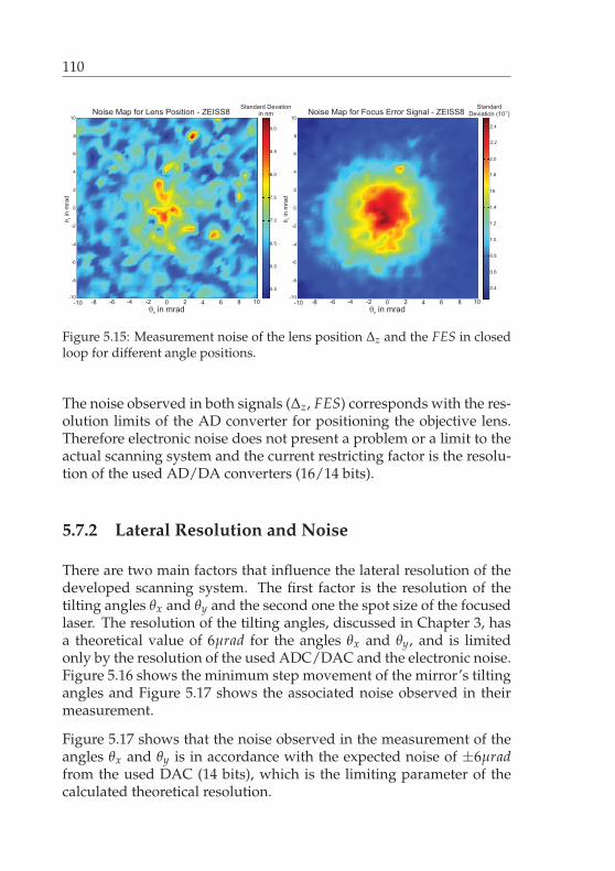
110
� in mradx
� in
mra
dy
-10 -8 -6 -4 0 2 4 6 8-10
-8
-6
-4
0
-2
2
4
6
8
10
5.5
6.5
7.5
8.5
8.0
7.0
9.0
6.0
-2 10
� in mradx
� in
mra
dy
-10 -8 -6 -4 0 2 4 6 8-10
-8
-6
-4
0
-2
2
4
6
8
10
0.8
16
2.4
1.2
2.0
-2 10
Standard Devation
in nmNoise Map for Lens Position - ZEISS8 Noise Map for Focus Error Signal - ZEISS8
0.4
Standard-3
Deviation (10 )
2.2
1.8
1.4
1.0
0.6
Figure 5.15: Measurement noise of the lens position Δz and the FES in closedloop for different angle positions.
The noise observed in both signals (Δz, FES) corresponds with the res-olution limits of the AD converter for positioning the objective lens.Therefore electronic noise does not present a problem or a limit to theactual scanning system and the current restricting factor is the resolu-tion of the used AD/DA converters (16/14 bits).
5.7.2 Lateral Resolution and Noise
There are two main factors that influence the lateral resolution of thedeveloped scanning system. The first factor is the resolution of thetilting angles θx and θy and the second one the spot size of the focusedlaser. The resolution of the tilting angles, discussed in Chapter 3, hasa theoretical value of 6μrad for the angles θx and θy, and is limitedonly by the resolution of the used ADC/DAC and the electronic noise.Figure 5.16 shows the minimum step movement of the mirror’s tiltingangles and Figure 5.17 shows the associated noise observed in theirmeasurement.
Figure 5.17 shows that the noise observed in the measurement of theangles θx and θy is in accordance with the expected noise of ±6μradfrom the used DAC (14 bits), which is the limiting parameter of thecalculated theoretical resolution.
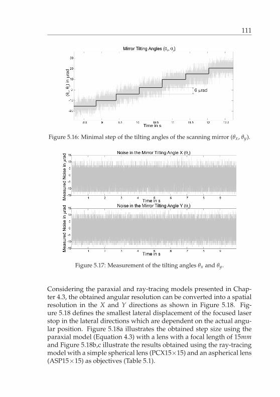
111
Figure 5.16: Minimal step of the tilting angles of the scanning mirror (θx, θy).
Figure 5.17: Measurement of the tilting angles θx and θy.
Considering the paraxial and ray-tracing models presented in Chap-ter 4.3, the obtained angular resolution can be converted into a spatialresolution in the X and Y directions as shown in Figure 5.18. Fig-ure 5.18 defines the smallest lateral displacement of the focused laserstop in the lateral directions which are dependent on the actual angu-lar position. Figure 5.18a illustrates the obtained step size using theparaxial model (Equation 4.3) with a lens with a focal length of 15mmand Figure 5.18b,c illustrate the results obtained using the ray-tracingmodel with a simple spherical lens (PCX15×15) and an aspherical lens(ASP15×15) as objectives (Table 5.1).
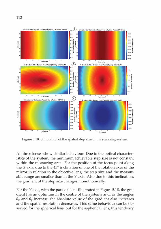
112
Figure 5.18: Simulation of the spatial step size of the scanning system.
All three lenses show similar behaviour. Due to the optical character-istics of the system, the minimum achievable step size is not constantwithin the measuring area. For the position of the focus point alongthe X axis, due to the 45◦ inclination of one of the rotation axes of themirror in relation to the objective lens, the step size and the measur-able range are smaller than in the Y axis. Also due to this inclination,the gradient of the step size changes monothonically.
For the Y axis, with the paraxial lens illustrated in Figure 5.18, the gra-dient has an optimum in the centre of the systems and, as the anglesθx and θy increase, the absolute value of the gradient also increasesand the spatial resolution decreases. This same behaviour can be ob-served for the spherical lens, but for the aspherical lens, this tendency
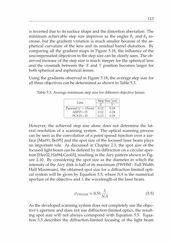
113
is inverted due to its surface shape and the distortion aberration. Theminimum achievable step size improves as the angles θx and θy in-crease, but the gradient variation is much smaller because of the as-pherical curvature of the lens and its residual barrel distortion. Bycomparing all the gradient maps in Figure 5.18, the influence of theuncompensated objectives in the step size can be clearly seen. The ob-served increase of the step size is much steeper for the spherical lensand the crosstalk between the X and Y position becomes larger forboth spherical and aspherical lenses.
Using the gradients observed in Figure 5.18, the average step size forall three objectives can be determined as shown in Table 5.3.
Table 5.3: Average minimum step size for different objective lenses.
Lens Step Size [μm]X Y
Paraxial ( f = 15mm) 0.12 0.18ASP15×15 0.12 0.18PCX15×15 0.13 0.19
However, the achieved step size alone does not determine the lat-eral resolution of a scanning system. The optical scanning processcan be seen as the convolution of a point spread function over a sur-face [Mar91, Bei95] and the spot size of the focused laser beam playsan important role. As discussed in Chapter 2.3, the spot size of thefocused light beam can be defined by its diffraction on a circular aper-ture [Hec02,Haf94,Gro03], resulting in the Airy pattern shown in Fig-ure 2.10. By considering the spot size as the diameter in which theintensity of the Airy disk is half of its maximum (FWHM - Full WidthHalf Maximum), the obtained spot size for a diffraction limited opti-cal system will be given by Equation 5.5, where NA is the numericalaperture of the objective and λ the wavelength of the laser beam.
�FWHM ≈ 0.51λ
NA(5.5)
As the developed scanning system does not completely use the objec-tive’s aperture and does not use diffraction-limited optics, the result-ing spot size will not always correspond with Equation 5.5. Equa-tion 5.5 describes the diffraction-limited focusing of the light beam
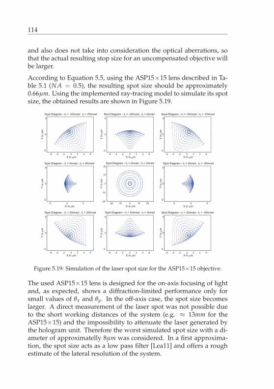
114
and also does not take into consideration the optical aberrations, sothat the actual resulting stop size for an uncompensated objective willbe larger.
According to Equation 5.5, using the ASP15×15 lens described in Ta-ble 5.1 (NA = 0.5), the resulting spot size should be approximately0.66μm. Using the implemented ray-tracing model to simulate its spotsize, the obtained results are shown in Figure 5.19.
Spot Diagram - �= -20mrad , �= 20mradx y
Y in
�m
X in �m
Spot Diagram - �= 0mrad , �= 20mradx y
Y in
�m
X in �m
Spot Diagram - �= 20mrad , �= 20mradx y
Y in
�m
X in �m
Spot Diagram - �= -20mrad , �= 0mradx y
Y in
�m
X in �m
Spot Diagram - �= -20mrad , �= -20mradx y
Y in
�m
X in �m
Spot Diagram - �= 0mrad , �= 0mradx y
Y in
nm
X in nm
Spot Diagram - �= 20mrad , �= 0mradx y
Y in
�m
X in �m
Spot Diagram - �= 0mrad , �= -20mradx y
Y in
�m
X in �m
Spot Diagram - �= 20mrad , �= -20mradx y
Y in
�m
X in �m
Figure 5.19: Simulation of the laser spot size for the ASP15×15 objective.
The used ASP15×15 lens is designed for the on-axis focusing of lightand, as expected, shows a diffraction-limited performance only forsmall values of θx and θy. In the off-axis case, the spot size becomeslarger. A direct measurement of the laser spot was not possible dueto the short working distances of the system (e.g. ≈ 13mm for theASP15×15) and the impossibility to attenuate the laser generated bythe hologram unit. Therefore the worst simulated spot size with a di-ameter of approximatelly 8μm was considered. In a first approxima-tion, the spot size acts as a low pass filter [Lea11] and offers a roughestimate of the lateral resolution of the system.
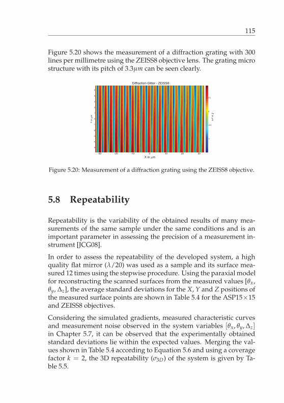
115
Figure 5.20 shows the measurement of a diffraction grating with 300lines per millimetre using the ZEISS8 objective lens. The grating microstructure with its pitch of 3.3μm can be seen clearly.
X in �m
Y in
�m
-30 -20 0 10 20 30
-5
-4
-3
-2
0
-1
1
2
3
4
5
-1
0
-0.5
0.5
-10
Z in
�m
Diffraction Gitter - ZEISS8
Figure 5.20: Measurement of a diffraction grating using the ZEISS8 objective.
5.8 Repeatability
Repeatability is the variability of the obtained results of many mea-surements of the same sample under the same conditions and is animportant parameter in assessing the precision of a measurement in-strument [JCG08].
In order to assess the repeatability of the developed system, a highquality flat mirror (λ/20) was used as a sample and its surface mea-sured 12 times using the stepwise procedure. Using the paraxial modelfor reconstructing the scanned surfaces from the measured values [θx,θy, Δz], the average standard deviations for the X, Y and Z positions ofthe measured surface points are shown in Table 5.4 for the ASP15×15and ZEISS8 objectives.
Considering the simulated gradients, measured characteristic curvesand measurement noise observed in the system variables [θx, θy, Δz]in Chapter 5.7, it can be observed that the experimentally obtainedstandard deviations lie within the expected values. Merging the val-ues shown in Table 5.4 according to Equation 5.6 and using a coveragefactor k = 2, the 3D repeatability (σ3D) of the system is given by Ta-ble 5.5.
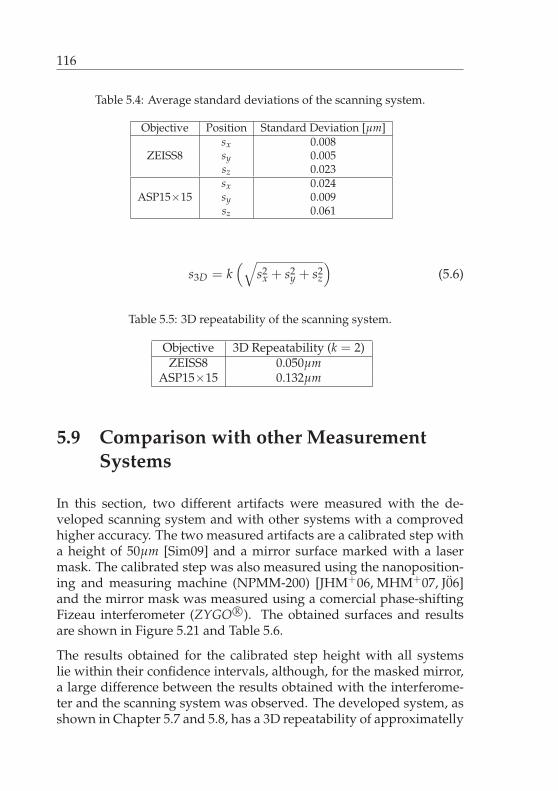
116
Table 5.4: Average standard deviations of the scanning system.
Objective Position Standard Deviation [μm]
ZEISS8sx 0.008sy 0.005sz 0.023
ASP15×15sx 0.024sy 0.009sz 0.061
s3D = k(√
s2x + s2
y + s2z
)(5.6)
Table 5.5: 3D repeatability of the scanning system.
Objective 3D Repeatability (k = 2)ZEISS8 0.050μm
ASP15×15 0.132μm
5.9 Comparison with other Measurement
Systems
In this section, two different artifacts were measured with the de-veloped scanning system and with other systems with a comprovedhigher accuracy. The two measured artifacts are a calibrated step witha height of 50μm [Sim09] and a mirror surface marked with a lasermask. The calibrated step was also measured using the nanoposition-ing and measuring machine (NPMM-200) [JHM+06, MHM+07, J0̈6]and the mirror mask was measured using a comercial phase-shiftingFizeau interferometer (ZYGO R©). The obtained surfaces and resultsare shown in Figure 5.21 and Table 5.6.
The results obtained for the calibrated step height with all systemslie within their confidence intervals, although, for the masked mirror,a large difference between the results obtained with the interferome-ter and the scanning system was observed. The developed system, asshown in Chapter 5.7 and 5.8, has a 3D repeatability of approximatelly
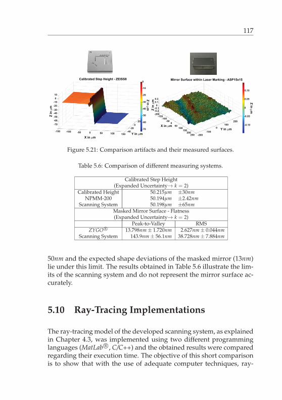
117
Figure 5.21: Comparison artifacts and their measured surfaces.
Table 5.6: Comparison of different measuring systems.
Calibrated Step Height(Expanded Uncertainty→ k = 2)
Calibrated Height 50.215μm ±30nmNPMM-200 50.194μm ±2.42nm
Scanning System 50.198μm ±65nmMasked Mirror Surface - Flatness(Expanded Uncertainty→ k = 2)
Peak-to-Valley RMSZYGO R© 13.798nm ± 1.720nm 2.627nm ± 0.044nm
Scanning System 143.9nm ± 56.1nm 38.728nm ± 7.884nm
50nm and the expected shape deviations of the masked mirror (13nm)lie under this limit. The results obtained in Table 5.6 illustrate the lim-its of the scanning system and do not represent the mirror surface ac-curately.
5.10 Ray-Tracing Implementations
The ray-tracing model of the developed scanning system, as explainedin Chapter 4.3, was implemented using two different programminglanguages (MatLab R©, C/C++) and the obtained results were comparedregarding their execution time. The objective of this short comparisonis to show that with the use of adequate computer techniques, ray-
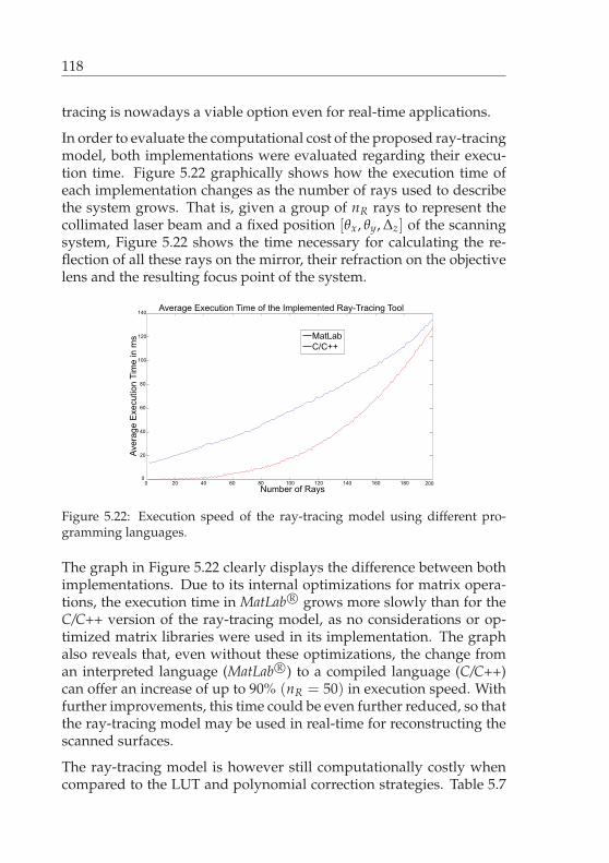
118
tracing is nowadays a viable option even for real-time applications.
In order to evaluate the computational cost of the proposed ray-tracingmodel, both implementations were evaluated regarding their execu-tion time. Figure 5.22 graphically shows how the execution time ofeach implementation changes as the number of rays used to describethe system grows. That is, given a group of nR rays to represent thecollimated laser beam and a fixed position [θx, θy, Δz] of the scanningsystem, Figure 5.22 shows the time necessary for calculating the re-flection of all these rays on the mirror, their refraction on the objectivelens and the resulting focus point of the system.
Figure 5.22: Execution speed of the ray-tracing model using different pro-gramming languages.
The graph in Figure 5.22 clearly displays the difference between bothimplementations. Due to its internal optimizations for matrix opera-tions, the execution time in MatLab R© grows more slowly than for theC/C++ version of the ray-tracing model, as no considerations or op-timized matrix libraries were used in its implementation. The graphalso reveals that, even without these optimizations, the change froman interpreted language (MatLab R©) to a compiled language (C/C++)can offer an increase of up to 90% (nR = 50) in execution speed. Withfurther improvements, this time could be even further reduced, so thatthe ray-tracing model may be used in real-time for reconstructing thescanned surfaces.
The ray-tracing model is however still computationally costly whencompared to the LUT and polynomial correction strategies. Table 5.7
119
shows a brief comparison of the time necessary for reconstructing asurface with 100× 100 points with each one of the methods introducedin Chapter 4.2.
Table 5.7: Average execution time of different error correction strategies.
Modelling and Error Correction Execution Time [s]Paraxial Model 0.012
Polynomials 0.067Look-up Table 0.302
Ray-Tracing Model (C/C++ ,nR = 50) 49.365Ray-Tracing Model (MatLab R©, nR = 50) 650.394
All the simulations shown in Figure 5.22 and Table 5.7 have been doneusing a workstation equipped with an AMD R© Phenom II X4 920 pro-cessor and 3 GB RAM running under Microsoft Windows XP R© Profes-sional SP3.

Chapter 6
Measurement Tasks andApplications
The main application of the developed system is the optical acqui-sition of 3D topographic information of microstructures, although thesystem also permits for example the measurement of macroscopic sur-faces for the observation of machining marks and material structures.Once the operation, functionality and main characteristics of the de-veloped scanning system have been fully described, this section willpresent a series of application examples of the system.
As discussed in previous chapters, the measurement of microstruc-tures is essential in many technical fields. In this section, a series ofdifferent microstructures were measured using the developed systemand the results are shown and discussed. The use of different objectivelenses is also compared. All the presented surfaces have been recon-structed using the LUT correction method presented in Chapter 4.4.1;the objective lenses used are indicated for each measurement.
The first samples presented in this section are a series of silicon struc-tures. Figure 6.1 and Figure 6.3 show a variety of measured surfacesusing the ZEISS8 and ASP15×15 lenses. The second presented sampleis a pinhole with a diameter of 600μm. Figure 6.2 shows the measuredsurface using the ASP15×15 lens. The third and last sample shownis a milled aluminium surface. Figure 6.4 shows the machining marksleft by the milling process.
All the samples shown illustrate the flexibility of the developed scan-ning system and its usage in a wide variety of measuring tasks.
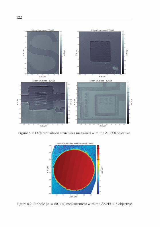
122
X in �m
Y in
�m
-100 -50 50
-200
-100
-150
-50
0
50
-2
-1
0
1
0
Z in
�m
Silicon Structures - ZEISS8
-150
-3
-4
X in �mY
in
�m
-100 -50 50 100
-150
-50
-100
50
0
150
0
1.0
0.5
1.5
0
Z in
�m
Silicon Structures - ZEISS8
-150
-0.5
-1.0
X in �m
Y in
�m
-60 -40 40 60
-20
20
0
40
60
80
0
1.0
-0.5
0.5
20
Z in
�m
Silicon Structures - ZEISS8
-80
-1.5
-2.0
X in �m
Y in
�m
0 20 60 80
0
20
40
-6
0
-4
4
40
Z in
�m
Silicon Structures - ZEISS8
-20
-8
-10
100 150
100
150
200
2
3
150
100
-1.5
-2.0
2.5
2.0
-40
-60
-80-20 0 80
2.0
2.5
1.5
-1.0
-2.5
60
80
-20
-40
-60
-80
-40-60-80-100 100
-12
-2
2
6
Figure 6.1: Different silicon structures measured with the ZEISS8 objective.
Precision Pinhole (600�m) - ASP15x15
X in �m
Y in
�m
-200 -100 0 100 200 300
-400
-300
-200
-100
0
100
200
300
-40
-20
0
20
10
-10
30
-30
-50
Z in
�m
Figure 6.2: Pinhole (� = 600μm) measurement with the ASP15×15 objective.
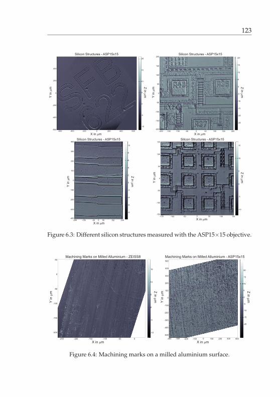
123
X in �m
Y in
�m
-400 -200 200 400-600
-200
-400
200
0
400
0
10
5
15
0
Z in
�m
Silicon Structures - ASP15x15
-600
-5
-10
X in �m
Y in
�m
-100-150 50 200
-150
-50
-100
50
150
200
0
10
5
15
100
Z in
�m
Silicon Structures - ASP15x15
-200
-5
-10
X in �m
Y in
�m
-150 -50 50 150
-300
-100
-200
200
300
400
0
4
2
10
0
Z in
�m
Silicon Structures - ASP15x15
-250
-2
-4
X in �m
Y in
�m
-100 -50 500
-100
0
-50
50
100
150
0
10
5
15
100
Z in
�m
Silicon Structures - ASP15x15
-150
-5
-10
600
20
100
0
-200
-50 0 150
20
-15
-25
-20
100
0
-400
250
8
6
-6
-8
-150
150
Figure 6.3: Different silicon structures measured with the ASP15×15 objective.
X in �m
Y in
�m
-200 -150 -50 0
-200
-100
-150
-50
0
50
0
10
5
15
-100
Z in
�m
Machining Marks on Milled Alluminium - ZEISS8
-250
-5
-10
X in �m
Y in
�m
-200 -100 300
-20
-500
-100
-400
100
0
500
0
10
5
15
100
Z in
�m
Machining Marks on Milled Alluminium - ASP15x15
-400
-5
-10
-300
-200
200
300
400
-300 0 200 400
20
-15
Figure 6.4: Machining marks on a milled aluminium surface.

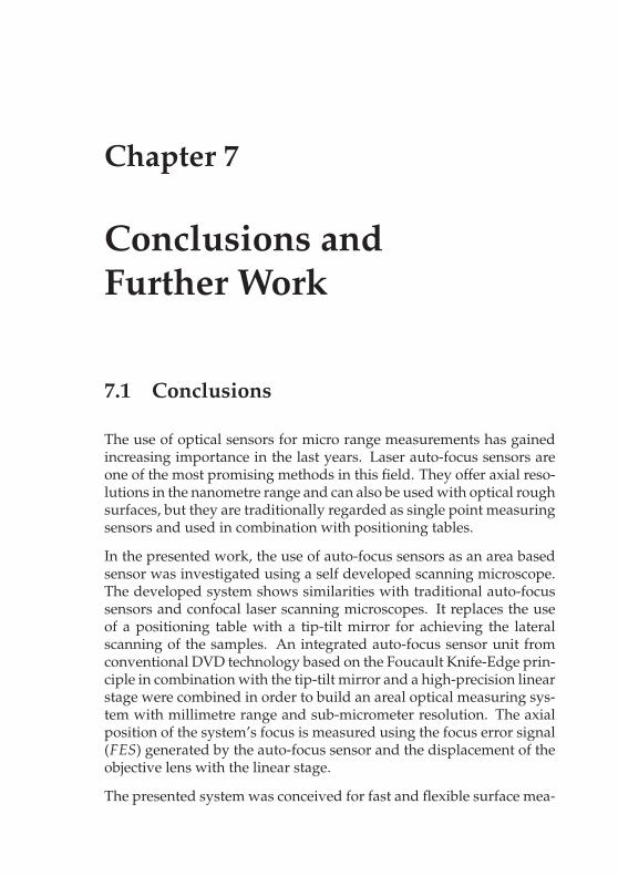
Chapter 7
Conclusions andFurther Work
7.1 Conclusions
The use of optical sensors for micro range measurements has gainedincreasing importance in the last years. Laser auto-focus sensors areone of the most promising methods in this field. They offer axial reso-lutions in the nanometre range and can also be used with optical roughsurfaces, but they are traditionally regarded as single point measuringsensors and used in combination with positioning tables.
In the presented work, the use of auto-focus sensors as an area basedsensor was investigated using a self developed scanning microscope.The developed system shows similarities with traditional auto-focussensors and confocal laser scanning microscopes. It replaces the useof a positioning table with a tip-tilt mirror for achieving the lateralscanning of the samples. An integrated auto-focus sensor unit fromconventional DVD technology based on the Foucault Knife-Edge prin-ciple in combination with the tip-tilt mirror and a high-precision linearstage were combined in order to build an areal optical measuring sys-tem with millimetre range and sub-micrometer resolution. The axialposition of the system’s focus is measured using the focus error signal(FES) generated by the auto-focus sensor and the displacement of theobjective lens with the linear stage.
The presented system was conceived for fast and flexible surface mea-
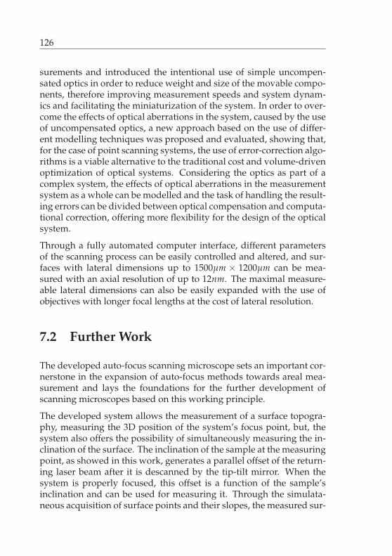
126
surements and introduced the intentional use of simple uncompen-sated optics in order to reduce weight and size of the movable compo-nents, therefore improving measurement speeds and system dynam-ics and facilitating the miniaturization of the system. In order to over-come the effects of optical aberrations in the system, caused by the useof uncompensated optics, a new approach based on the use of differ-ent modelling techniques was proposed and evaluated, showing that,for the case of point scanning systems, the use of error-correction algo-rithms is a viable alternative to the traditional cost and volume-drivenoptimization of optical systems. Considering the optics as part of acomplex system, the effects of optical aberrations in the measurementsystem as a whole can be modelled and the task of handling the result-ing errors can be divided between optical compensation and computa-tional correction, offering more flexibility for the design of the opticalsystem.
Through a fully automated computer interface, different parametersof the scanning process can be easily controlled and altered, and sur-faces with lateral dimensions up to 1500μm × 1200μm can be mea-sured with an axial resolution of up to 12nm. The maximal measure-able lateral dimensions can also be easily expanded with the use ofobjectives with longer focal lengths at the cost of lateral resolution.
7.2 Further Work
The developed auto-focus scanning microscope sets an important cor-nerstone in the expansion of auto-focus methods towards areal mea-surement and lays the foundations for the further development ofscanning microscopes based on this working principle.
The developed system allows the measurement of a surface topogra-phy, measuring the 3D position of the system’s focus point, but, thesystem also offers the possibility of simultaneously measuring the in-clination of the surface. The inclination of the sample at the measuringpoint, as showed in this work, generates a parallel offset of the return-ing laser beam after it is descanned by the tip-tilt mirror. When thesystem is properly focused, this offset is a function of the sample’sinclination and can be used for measuring it. Through the simulata-neous acquisition of surface points and their slopes, the measured sur-
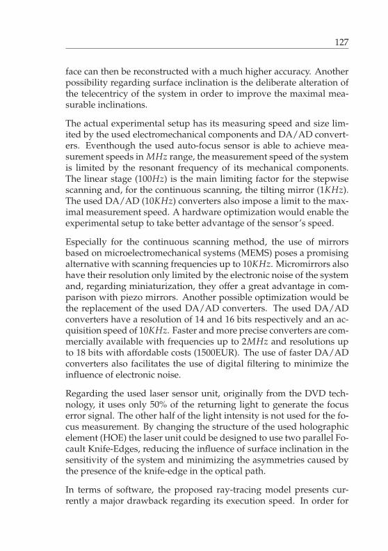
127
face can then be reconstructed with a much higher accuracy. Anotherpossibility regarding surface inclination is the deliberate alteration ofthe telecentricy of the system in order to improve the maximal mea-surable inclinations.
The actual experimental setup has its measuring speed and size lim-ited by the used electromechanical components and DA/AD convert-ers. Eventhough the used auto-focus sensor is able to achieve mea-surement speeds in MHz range, the measurement speed of the systemis limited by the resonant frequency of its mechanical components.The linear stage (100Hz) is the main limiting factor for the stepwisescanning and, for the continuous scanning, the tilting mirror (1KHz).The used DA/AD (10KHz) converters also impose a limit to the max-imal measurement speed. A hardware optimization would enable theexperimental setup to take better advantage of the sensor’s speed.
Especially for the continuous scanning method, the use of mirrorsbased on microelectromechanical systems (MEMS) poses a promisingalternative with scanning frequencies up to 10KHz. Micromirrors alsohave their resolution only limited by the electronic noise of the systemand, regarding miniaturization, they offer a great advantage in com-parison with piezo mirrors. Another possible optimization would bethe replacement of the used DA/AD converters. The used DA/ADconverters have a resolution of 14 and 16 bits respectively and an ac-quisition speed of 10KHz. Faster and more precise converters are com-mercially available with frequencies up to 2MHz and resolutions upto 18 bits with affordable costs (1500EUR). The use of faster DA/ADconverters also facilitates the use of digital filtering to minimize theinfluence of electronic noise.
Regarding the used laser sensor unit, originally from the DVD tech-nology, it uses only 50% of the returning light to generate the focuserror signal. The other half of the light intensity is not used for the fo-cus measurement. By changing the structure of the used holographicelement (HOE) the laser unit could be designed to use two parallel Fo-cault Knife-Edges, reducing the influence of surface inclination in thesensitivity of the system and minimizing the asymmetries caused bythe presence of the knife-edge in the optical path.
In terms of software, the proposed ray-tracing model presents cur-rently a major drawback regarding its execution speed. In order for

128
it to become a viable option, further programming optimizations arenecessary to reduce its execution time.
The system was tested using a high-end microscope objective and out-of-the-shelf spherical and aspherical lenses as objectives. With the useof the proposed error correction strategies, a single aspherical lenscould be designed for the specific application, focusing on the opti-mization of the spot size across the whole working range in detrimentof characteristics such as distortion and field curvature, which can becomputationally corrected.
The prerequisites of all the further improvements and works proposedin this section were layed by this work.
List of Figures
1.1 The nanopositioning and measuring machine (NPMM)developed in Ilmenau. . . . . . . . . . . . . . . . . . . . 3
1.2 Conceptual diagram of the proposed optical pre-scanningsystem. . . . . . . . . . . . . . . . . . . . . . . . . . . . . 5
2.1 Image formation on a thin lens. . . . . . . . . . . . . . . 112.2 Ray-tracing general procedure. . . . . . . . . . . . . . . 122.3 Ray-tracing flowchart. . . . . . . . . . . . . . . . . . . . 132.4 Models for optical imaging. . . . . . . . . . . . . . . . . 172.5 Third-order optical aberrations. . . . . . . . . . . . . . . 182.6 Barrel and pincushion distortion in a grid. . . . . . . . . 192.7 Basic compound microscope and its optical path. . . . . 202.8 Misky’s confocal microscope [Min61]. . . . . . . . . . . 212.9 Basic principle of confocal microscopes. . . . . . . . . . 222.10 Fraunhofer-diffraction on a circular aperture. . . . . . . 232.11 Rayleigh and sparrow resolution criteria. . . . . . . . . 252.12 Diagram of the astigmatic method for detection of the
focus error signal (FES). . . . . . . . . . . . . . . . . . . 272.13 Typical focus error signal (FES) curve. . . . . . . . . . . 282.14 Beam path of the collinear astigmatic method. . . . . . 292.15 The two planes of the astigmatic lens. . . . . . . . . . . 302.16 Two-dimensional gaussian distribution on the quadrant
diode. . . . . . . . . . . . . . . . . . . . . . . . . . . . . . 322.17 Diagram of the knife-edge method for detection of the
focus error signal (FES). . . . . . . . . . . . . . . . . . . 332.18 Beam path of the knife-edge method. . . . . . . . . . . . 342.19 Focus error detection with the obscuration method. . . 352.20 Types of optical beam scanning. . . . . . . . . . . . . . . 362.21 Lateral scanning in confocal microscopy. . . . . . . . . . 37
130
3.1 Optical schema of the scanning system and its main com-ponents. . . . . . . . . . . . . . . . . . . . . . . . . . . . 42
3.2 Miniaturized hologram laser unit [YMO+00]. . . . . . . 423.3 Developed laser scanning microscope (1-Hologram Laser
Unit; 2-Tilting Mirror; 3-Camera Lens; 4-Camera; 5-Po-larized Beam Splitter; 6-Linear Stage; 7-Objective). . . . 44
3.4 Telecentricity in the scanning system. . . . . . . . . . . 463.5 Telecentricity on the image space and system defocus. . 473.6 Typical signals during the stepwise and continuous scan-
ning procedure. . . . . . . . . . . . . . . . . . . . . . . . 483.7 System control signals and data acquisition. . . . . . . . 50
4.1 Surface reconstruction using error correction. . . . . . . 564.2 Basic concepts of model based error correction. . . . . . 584.3 Simplified 2D schematic of the scanning system. . . . . 594.4 Schematic diagram of the used 2D tilting mirror. . . . . 604.5 Simplified 3D paraxial schematic of the scanning system. 614.6 Lateral displacement of the focus point in the 3D parax-
ial model with f ′ob = 15mm. . . . . . . . . . . . . . . . . 624.7 Considerations on the non-collinear focus detection in
scanning systems. . . . . . . . . . . . . . . . . . . . . . . 634.8 Complete 2D optical schema of the focus detection for
the scanning system. . . . . . . . . . . . . . . . . . . . . 644.9 Integration boundaries for the non-collinear obscura-
tion method. . . . . . . . . . . . . . . . . . . . . . . . . . 654.10 Simulation of the FES using the paraxial model. . . . . 664.11 Influence of optical aberrations using a simple spherical
lens ( f = 15mm). . . . . . . . . . . . . . . . . . . . . . . 684.12 Mathematical representation of the scanning system for
ray-tracing modelling. . . . . . . . . . . . . . . . . . . . 694.13 Definition of the direction vectors Dke and Dpd. . . . . . 704.14 Representation of the kinematic chain of the ray-tracing
model. . . . . . . . . . . . . . . . . . . . . . . . . . . . . 714.15 Simulation of the focus error signal FES using the ray-
tracing model. . . . . . . . . . . . . . . . . . . . . . . . . 734.16 Influence of optical aberrations on the FES for β = 0◦. . 744.17 Example model for current measurement. . . . . . . . . 754.18 Basic calibration concept for the laser scanning micro-
scope. . . . . . . . . . . . . . . . . . . . . . . . . . . . . . 78
131
4.19 Laser scanning microscope as a black box. . . . . . . . . 814.20 Conceptual design for the direct measurement of FLSM. 824.21 Conceptual design for the direct measurement of FLSM. 824.22 1D Look-up table of a sinusoidal function. . . . . . . . . 834.23 Describing FLSM with a look-up table. . . . . . . . . . . 84
5.1 Characteristic curve of the system for different positions(θx, θy). . . . . . . . . . . . . . . . . . . . . . . . . . . . . 90
5.2 Measured S-Curve slope for different mirror tip-tilt an-gles (θx, θy). . . . . . . . . . . . . . . . . . . . . . . . . . 91
5.3 Simulation of the error coefficients of the system usingthe paraxial and ray-tracing models. . . . . . . . . . . . 94
5.4 Surface of a λ/20 flat mirror using the paraxial model(ASP15×15). . . . . . . . . . . . . . . . . . . . . . . . . . 98
5.5 Surface of a λ/20 mirror using different correction meth-ods (ASP15×15). . . . . . . . . . . . . . . . . . . . . . . 99
5.6 Surface of a λ/20 flat mirror using the paraxial model(ZEISS8). . . . . . . . . . . . . . . . . . . . . . . . . . . . 100
5.7 Surface of a λ/20 mirror using different correction meth-ods (ZEISS8). . . . . . . . . . . . . . . . . . . . . . . . . . 101
5.8 Surface of a λ/20 mirror using the ray-tracing modelwith and without calibration. . . . . . . . . . . . . . . . 103
5.9 Maximum measureable surface inclination. . . . . . . . 1045.10 Influence of the sample inclination on the FES. . . . . . 1065.11 Maximum measurable angle in a steel sphere (� = 2mm).1065.12 Non-telecentric ilumination and maximum measurable
angle. . . . . . . . . . . . . . . . . . . . . . . . . . . . . . 1075.13 Minimal step of the linear stage of the objective lens (Δz). 1085.14 Measurement of the lens position Δz and the FES in
closed loop. . . . . . . . . . . . . . . . . . . . . . . . . . 1095.15 Measurement noise of the lens position Δz and the FES
in closed loop for different angle positions. . . . . . . . 1105.16 Minimal step of the tilting angles of the scanning mirror
(θx, θy). . . . . . . . . . . . . . . . . . . . . . . . . . . . . 1115.17 Measurement of the tilting angles θx and θy. . . . . . . . 1115.18 Simulation of the spatial step size of the scanning system.1125.19 Simulation of the laser spot size for the ASP15×15 ob-
jective. . . . . . . . . . . . . . . . . . . . . . . . . . . . . 114
132
5.20 Measurement of a diffraction grating using the ZEISS8objective. . . . . . . . . . . . . . . . . . . . . . . . . . . . 115
5.21 Comparison artifacts and their measured surfaces. . . . 1175.22 Execution speed of the ray-tracing model using differ-
ent programming languages. . . . . . . . . . . . . . . . 118
6.1 Different silicon structures measured with the ZEISS8objective. . . . . . . . . . . . . . . . . . . . . . . . . . . . 122
6.2 Pinhole (� = 600μm) measurement with the ASP15×15objective. . . . . . . . . . . . . . . . . . . . . . . . . . . . 122
6.3 Different silicon structures measured with the ASP15×15 objective. . . . . . . . . . . . . . . . . . . . . . . . . . 123
6.4 Machining marks on a milled aluminium surface. . . . 123
List of Tables
2.1 Typical characteristics of commercial confocal scanningsystems. . . . . . . . . . . . . . . . . . . . . . . . . . . . 39
3.1 Specification of the system’s components. . . . . . . . . 453.2 Average measurement frequency of the scanning meth-
ods. . . . . . . . . . . . . . . . . . . . . . . . . . . . . . . 493.3 Resolution limits of the used AD/DA converters. . . . 51
4.1 Parameters for the paraxial simulation of the FES basedon the designed system. . . . . . . . . . . . . . . . . . . 66
4.2 Origin and normal vectors of the ray-tracing components. 724.3 Homogeneous transformations of the ray-tracing model. 72
5.1 Parameters and coefficients of the used lenses. . . . . . 905.2 Calibrated parameters of the ray-tracing model. . . . . 975.3 Average minimum step size for different objective lenses. 1135.4 Average standard deviations of the scanning system. . 1165.5 3D repeatability of the scanning system. . . . . . . . . . 1165.6 Comparison of different measuring systems. . . . . . . 1175.7 Average execution time of different error correction strate-
gies. . . . . . . . . . . . . . . . . . . . . . . . . . . . . . . 119

Bibliography
[Bar85] Egbert Barthel. Ein Beitrag zu berührungslosen Antastver-fahren, dargestellt an Varianten des Fokussierverfahrens. Ph.d.thesis, Technische Hochschule Ilmenau, 1985.
[Bas95] Michael Bass. Handbook of Optics. McGraw-Hill Inc., 2ndedition, 1995.
[Bei95] Leo Beiser. Fundamental architecture of optical scanningsystems. Applied Optics, 34(31):7307, November 1995.
[Bit03] Frank Bitte. Ein Spiegelmatrix-basiertes optisches 3D-Messsystem für die Mikrostrukturprüfung. Ph.d. thesis,RWTH AAchen, 2003.
[BL76] Claude Bricot and Jean Claude Lehureau. Optical Focus-ing Device. US Patent 4,023,033, 1976.
[BM92] Bruce E. Bernacki and Masud Mansuripur. Diffractionanalysis and evaluation of several focus- and track-errordetection schemes for magneto-optical disk systems. InProc. SPIE 1316, Optical Data Storage, 150, pages 150–156,August 1992.
[BM94] Bruce E. Bernacki and Masud Mansuripur. Causes offocus-error feedthrough in optical-disk systems: astig-matic and obscuration methods. Applied optics, 33(5):735–43, February 1994.
[Bog07] Robert Bogue. Nanometrology: a critical discipline forthe twenty-first century. Sensor Review, 27(3):189–196,2007.
[BR91] Jos Benschop and Gerard Van Rosmalen. Confocal com-pact scanning optical microscope based on compact disctechnology. Applied Optics, 30(10):1179–1184, 1991.
136
[CFD05] Nathan S. Claxton, Thomas J. Fellers, and Michael W.Davidson. Laser Scanning Confocal Microscopy, 2005.
[CGLL84] Donald Kenneth Cohen, Wing Ho Gee, M. Ludeke, andJulian Lewkowicz. Automatic focus control: the astig-matic lens approach. Applied Optics, 23(4):565, February1984.
[Cho06] Hyungsuck Cho. Optomechatronics: Fusion of Optical andMechatronic Engineering. CRC Press, 1 edition, 2006.
[CK96] Timothy R. Corle and Gordon S. Kino. Confocal ScanningOptical Microscopy and Related Imaging Systems. AcademicPress, 1996.
[CNY+00] James Carriere, Raghu Narayan, Wei-Hung Yeh, ChubingPeng, Pramod Khulbe, Lifeng Li, Robert Anderson, Jin-han Choi, and Masud Mansuripur. Principles of opticaldisk data storage. Progress in Optics, 41:97–179, 2000.
[Coh87] Donald Kenneth Cohen. Analysis of Methods for DetectingFocus Error in Optical Data Storage Systems. Ph.d. thesis,University of Arizona, 1987.
[DDX+10] Hans-ulrich Danzebrink, Thorsten Dziomba, M. Xu,A. Pidduck, Richard K. Leach, Andrew Yacoot, andLudger Koenders. Scanning Probe Microscopy, Scan-ning Electron Microscopy and Critical Dimension:Nanometrology Status and Future Needs Within Europe.Technical report, Co-Nanomet Consortium, 2010.
[DIN99] DIN. DIN 1319-4: Grundlagen der Meßtechnik, 1999.
[Fab09] Markus Fabich. Advancing Confocal Laser Scanning Mi-croscopy. Optik & Photonik, 4(2):40–43, June 2009.
[FMT99] A. Flammini, D. Marioli, and A. Taroni. Applicationof an optimal look-up table to sensor data processing.IEEE Transactions on Instrumentation and Measurement,48(4):813–816, 1999.
[FY05] Hiroya Fukatsu and Kazuhisa Yanagi. Development ofan optical stylus displacement sensor for surface profiling
137
instruments. Microsystem Technologies, 11(8-10):582–589,August 2005.
[Gas02] Kjell J. Gasvik. Optical Metrology. John Wiley & Sons Inc.,West Sussex, 3rd edition, 2002.
[GD10] P S Gandhi and S Deshmukh. A 2D optomechanical fo-cused laser spot scanner: analysis and experimental re-sults for microstereolithography. Journal of Micromechan-ics and Microengineering, 20(1), January 2010.
[GM11] Luciano Selva Ginani and José Maurício S. T. Motta. The-oretical and Practical Aspects of Robot Calibration withExperimental Verification. Journal of the Brazilian Societyof Mechanical Sciences and Engineering, 33(1):15–21, 2011.
[Gra07] Duncan Graham. Nanometrology–is it the next big thingin measurement? The Analyst, 132(2):95–6, February 2007.
[Gro03] Rudolf Gross. Optik und Quantenphänomene, 2003.
[GT09] Luciano Selva Ginani and René Theska. Development ofa Software Simulation Tool for Movable Optic Compo-nents. In International Congress of Mechanical Engineering -COBEM, page 6, Gramado, 2009. ABCM.
[GT10] Luciano Selva Ginani and René Theska. Investigationof Opto-Mechanical Scanning Systems with the use of aRay-Tracing Tool. In Proceedings of EUSPEN, pages 148–151, Delft, 2010. EUSPEN.
[GVY05] Yuval Garini, Bart J Vermolen, and Ian T Young. Frommicro to nano: recent advances in high-resolution mi-croscopy. Current opinion in biotechnology, 16(1):3–12,February 2005.
[Hac10] Tobias Hackel. Grundlegende Untersuchungen zu vertikalenPositioniersystemen für Nanopräzisionsmaschinen. Ph.d. the-sis, Technische Universität Ilmenau, 2010.
[Haf94] Heinz Haferkorn. Optik: Physikalish-technische Grundlagenund Anwendungen. Barth, Leipzig, 3 edition, 1994.
[HBVS03] Bohumil Hnilicka, Alina Besancon-Voda, and Heinz-JörgSchröder. Modelling the Focus Error Signal Generation
138
in a DVD Player. In IMACS Multiconference ComputationalEngineering Systems Applications, pages 11–18, Lille, 2003.IEEE.
[HCHD06] H.N. Hansen, K. Carneiro, H. Haitjema, and L. DeChiffre. Dimensional Micro and Nano Metrology. CIRPAnnals - Manufacturing Technology, 55(2):721–743, January2006.
[Hec02] Eugene Hecht. Optik. Oldenbourg GmbH, München, 4edition, 2002.
[Her01] Martin Hermann. Numerische Mathematik. OldenbourgGmbH, München, 2001.
[HTB+06] Günter Höhne, René Theska, Torsten Brix, Markus Lotz,Thomas Frank, and Tobias Hackel. Design of high preci-sion positioning and measuring machines using virtualprototyping. ABCM Symposium Series in Mechatronics,2:485–492, 2006.
[Hul07] Angela Hullmann. Measuring and assessing the devel-opment of nanotechnology. Scientometrics, 70(3):739–758,March 2007.
[IEE90] IEEE. IEEE Std 610.12-1990 - Standard Glossary of SoftareEngineering Terminology, 1990.
[J0̈6] Gerd Jäger. Precision Mechatronics - Nanomeasuring andNanopositioning Engineering at the Technische Univer-sität Ilmenau. In Proceedings of the 3rd Vietnam Conferenceon Mechatronics, Hanoi, 2006.
[JCG08] JCGM. JCGM 100:2008 - Evaluation of measurement data- Guide to the expression of uncertainty in measurement,2008.
[JHM+06] Gerd Jäger, Tino Hausotte, Eberhard Manske, H.-J. Büch-ner, Rostyslav Mastylo, N Dorozhovets, and N Hofmann.Nanomeasuring and nanopositioning engineering. Pro-ceedings of SPIE, pages 628001–628001–9, 2006.
[Kni03] S. Knight. Overview of NIST metrology development forthe semiconductor industry. In 11th IEEE International
139
Conference on Advanced Thermal Processing of Semiconduc-tors. RTP 2003, pages 35–44. IEEE, 2003.
[Kra00] Werner Krause. Gerätekonstruktion in Feinwerktechnik undElektronik. Carl Hanser GmbH, München, 3. edition, 2000.
[Kre06] Erwin Kreyszig. Advanced Engineering Mathematics. JohnWiley & Sons Inc., 9th edition, 2006.
[LBB+10] Richard K. Leach, Robert Boyd, Theresa Burke, Hans-ulrich Danzebrink, Kai Dirscherl, Thorsten Dziomba,Mark Gee, Ludger Koenders, Valérie Morazzani, Deb-dulal Roy, Wolfgang E S Unger, and Andrew Yacoot.Consultation on a European Strategy for Nanometrology.Technical report, Co-Nanomet Consortium, 2010.
[Lea11] Richard Leach, editor. Optical Measurement of Surface To-pography. Springer Berlin Heidelberg, Berlin, Heidelberg,2011.
[Lin94] Psang Dain Lin. Modeling for optical ray tracing anderror analysis. Mathematical and Computer Modelling,19(12):37–48, June 1994.
[Mar85] Gerald F. Marshall. Laser Beam Scanning. Marcel DekkerInc., New York, 1985.
[Mar91] Gerald F. Marshall. Optical Scanning. Marcel Dekker Inc.,New York, 1991.
[Mas05] Rostyslav Mastylo. A focus sensor for an application ina nanopositioning and nanomeasuring machine. Proceed-ings of SPIE, 5856(June):238–244, 2005.
[Mas12] Rostyslav Mastylo. Optische und Taktile Nanosensorenauf der Grundlage des Fokusverfahrens für die Anwendungin Nanopositionier- und Nanomessmaschinen. Ph.d. thesis,Technische Universität Ilmenau, 2012.
[Mer84] Peter-Michael Merbach. Untersuchungen über die Real-isierungsmöglichkeiten des berührungslosen Antastens beiautomatisierten Dreikoordinaten-Längenmeßeinrichtungen.Ph.d. thesis, Technische Hochschule Ilmenau, 1984.
140
[MHM+07] Eberhard Manske, Tino Hausotte, Rostyslav Mastylo,T Machleidt, K-H Franke, and Gerd Jäger. New appli-cations of the nanopositioning and nanomeasuring ma-chine by using advanced tactile and non-tactile probes.Measurement Science and Technology, 18(2):520–527, 2007.
[Min61] Marvin Minsky. Microscopy Apparatus. US Patent3,013,467, 1961.
[MMJ04] Rostyslav Mastylo, Eberhard Manske, and Gerd Jäger.Entwicklung eines Fokussensors und Integration in dieNanopositionier- und Nanomessmaschine. tm - Technis-ches Messen, 71(11/2004):596–602, 2004.
[MPM05] Steven A. Miller, James Pond, and Bernhard Michel. Ray-tracing trifft Maxwell-Gleichungen : Über die Integra-tion von mikro- und makrooptischem Design. Photonik,6, June 2005.
[MS97] Masud Mansuripur and Glenn Sincerbox. Principles andtechniques of optical data storage. Proceedings of the IEEE,85(11):1780–1796, 1997.
[NS92] Helmut Naumann and Gottfried Schröder. Bauelementeder Optik. Carl Hanser GmbH, München, 6 edition, 1992.
[Pac08] Hugo Pacheco. Ray Tracing in Industry. Technical report,Minho University, Braga, 2008.
[Paw06] James B. Pawley, editor. Handbook of Biological ConfocalMicroscopy. Springer Science+Business Media, New York,3rd edition, 2006.
[PBMH02] Timothy J. Purcell, Ian Buck, William R. Mark, and PatHanrahan. Ray tracing on programmable graphics hard-ware. ACM Transactions on Graphics, 21(3), July 2002.
[Phi03] George McArtney Phillips. Interpolation and Appoximationby Polynomials. Springer Verlag, New York, 2003.
[Phy03] Physik Instrumente. S-334 Tip/Tilt Mirror, 2003.
[Pol] Mikhail Polyanskiy. Refractive Index Database.http://refractiveindex.info/.
141
[Rie88] Horst Riesenberg. Handbuch der Mikroskopie. VEB VerlagTechnik, Berlin, 3 edition, 1988.
[Sch82] Manfred Schilling. Konstruktionsprinzipien der Gerätetech-nik. Habilitation thesis, Technische Hochschule Ilmenau,1982.
[She93] Song Shen. Theoretical models and comparison of threefocus-error detection methods. In Proceedings of SPIE, vol-ume 2053, pages 144–149. SPIE, 1993.
[Sim09] Simetrics. Vertical Standard VS, 2009.
[SM62] G. H. Spencer and M. V. R. K. Murty. General Ray-Tracing Procedure. Journal of the Optical Society of America,52(6):672, June 1962.
[SMGH95] K.-P. Schröder, W. Mirandé, H. Geuther, and C. Her-rmann. In quest of nm accuracy: supporting opticalmetrology by rigorous diffraction theory and AFM topog-raphy. Optics Communications, 115:568–575, 1995.
[SS97] C.J.R. Sheppard and D.M. Shotton. Confocal Laser Scan-ning Microscopy. BIOS Scientific Publishers, Oxford, 1997.
[SS02] Mark L. Schattenburg and Henry I. Smith. The criticalrole of metrology in nanotechnology. In Martin C. Peck-erar and Michael T. Postek, Jr., editors, Proceedings of SPIE,pages 116–124, Gaithersburg, July 2002. SPIE.
[TFHL04] René Theska, Thomas Frank, Tobias Hackel, and MarkusLotz. Design Principles for Highest Precision Applica-tions. In Proceedings of ASPE, page 4, Orlando, 2004.ASPE.
[The88] René Theska. Berürungslos-optische Antastung von Mes-sobjekten unter ausnutzung astigmatischer Abbildungseigen-schaften. Ph.d. thesis, Technische Hochschule Ilmenau,1988.
[TV98] Emanuele Trucco and Alessandro Verri. Introductory Tech-niques for 3S Computer Vision. Prentice Hall Inc., 1998.
[UU12] Michael Ulbrich and Stefan Ulbrich. Nichtlineare Opti-mierung. Springer Basel, Basel, 2012.
142
[vdB07] Adriaan van den Bos. Parameter Estimation for Scientistsand Engineers. John Wiley & Sons Inc., New Jersey, 1 edi-tion, 2007.
[Web96] Robert H. Webb. Confocal optical microscopy. Reports onProgress in Physics, 59:427–471, 1996.
[WPH06] A Weckenmann, G Peggs, and J Hoffmann. Probing sys-tems for dimensional micro- and nano-metrology. Mea-surement Science and Technology, 17(3):504–509, March2006.
[XRJR07] Peng Xi, Bartlomiej Rajwa, James T. Jones, and J. PaulRobinson. The design and construction of a cost-efficientconfocal laser scanning microscope. American Journal ofPhysics, 75(3):203, 2007.
[YMO+00] Shinya Yoshida, Kohji Minami, Kuniaki Okada, HiroyukiYamamoto, Tetsuo Ueyama, Keiji Sakai, and Yukio Ku-rata. Optical Pickup Employing a Hologram-Laser-Photodiode Unit. Japanese Journal of Applied Physics,39(2):877–882, 2000.

Liste der bisher erschienenen Bände, Stand 01.07.2013 Bericht aus dem Institut für Maschinenelemente und Konstruktion (IMK), 1990 – 2010 Band 1 Institut für Maschinenelemente und Konstruktion der TU Ilmenau
(Hrsg.): Forschung und Lehre im Institut für Maschinenelemente und Konstruktion (Institutsbericht) Ilmenau : ISLE, 1999. - ISBN 3-932633-37-7
Band 2 Spiller, Frank: Möglichkeiten der rechentechnischen Umsetzung von Erkenntnissen aus der Konstruktions-systematik unter Nutzung der Featuretechnologie (Dissertation TU Ilmenau 1998) Ilmenau : ISLE, 1998. - ISBN 3-932633-20-2
Band 3 Leibl, Peter: Entwicklung eines featureorientierten Hilfsmittels für die Konstruktion kostengünstiger Produkte (Dissertation TU Ilmenau 1998) Ilmenau : ISLE, 1998. - ISBN 3-00-003695-4
Band 4 Lutz, Steffen: Kennlinie und Eigenfrequenzen von Schraubenfedern (Dissertation TU Ilmenau 2000) Ilmenau : ISLE, 2000. - ISBN 3-932633-47-4
Band 5 Kletzin, Ulf: Finite-Elemente-basiertes Entwurfssystem für Federn und Federanforderungen (Dissertation TU Ilmenau 2000) Ilmenau : ISLE, 2000. - ISBN 3-932633-48-2
Band 6 Volz, Andreas K.: Systemorientierter Karosserie-Konzeptentwurf am Beispiel der Crashsimulation (Dissertation TU Ilmenau 1998) Ilmenau : ISLE, 2000. - ISBN 3-932633-52-0
Band 7 Brix, Torsten: Feature- und constraint-basierter Entwurf technischer Prinzipe (Dissertation TU Ilmenau 2001) Ilmenau : ISLE, 2001. - ISBN 3-932633-67-9

Band 8 Rektor der TU Ilmenau und Institut für Maschinenelemente und Konstruktion der TU Ilmenau (Hrsg.) in Zusammenarbeit mit Carl Zeiss Jena GmbH Vom Arbeitsblatt zum virtuellen Prototyp – 50 Jahre Konstruktionssystematik (Institutsbericht) Ilmenau : ISLE, 2002. - ISBN 3-932633-68-7
Band 9 Liebermann, Kersten: Rechnergestütztes Entwurfs- und Optimierungssystem für Schraubendruckfedern (Dissertation TU Ilmenau 2003) Ilmenau : ISLE, 2003. - ISBN 3-932633-74-1
Band 10 Meissner, Manfred; Denecke, Klaus: Die Geschichte der Maschinenelemente als Fachgebiet und Institut an der Technischen Universität Ilmenau von 1953 bis 2003 (Institutsbericht) Ilmenau : ISLE, 2003. - ISBN 3-932633-82-2
Band 11 Geinitz, Veronika: Genauigkeits- und auslastungsoptimierte Schraubendruckfedern (Dissertation TU Ilmenau 2006) Ilmenau : ISLE, 2006. - ISBN 3-938843-11-X
Band 12 Institut für Maschinenelemente und Konstruktion (Hrsg.): Festschrift zum Ehrenkolloquium anlässlich der Emeritierungen von Univ.-Prof. Dr.-Ing. habil. Dr. h.c. Günter Höhne und Univ.-Prof. Dr.-Ing. habil. Hans-Jürgen Schorcht (Institutsbericht) Ilmenau : ISLE, 2005. -ISBN 3-932633-97-0
Band 13 Wittkopp, Tobias: Mehrkörpersimulation von Schraubendruckfedern (Dissertation TU Ilmenau 2005) Ilmenau : ISLE, 2005. - ISBN 3-938843-07-1
Band 14 Frank, Stefan: Justierdrehen – eine Technologie für Hochleistungsoptik (Dissertation TU Ilmenau 2007) Ilmenau : ISLE, 2008. - ISBN 978-3-938843-35-4
Band 15 Schilling, Thomas: Augmented Reality in der Produktentstehung (Dissertation TU Ilmenau 2008) Ilmenau : ISLE, 2008. - ISBN 978-3-938843-42-0

Band 16 Lotz, Markus: Konstruktion von Messspiegeln hochgenauer Mess- und Positioniermaschinen (Dissertation TU Ilmenau 2009) Ilmenau : ISLE, 2009. - ISBN 978-3-938843-46-8
[Band 17] Hackel, Tobias: Grundlegende Untersuchungen zu vertikalen Positioniersystemen für Nanopräzisionsmaschinen (Dissertation TU Ilmenau 2010) Münster, Westf : Monsenstein und Vannerdat, 2010. - ISBN 978-3-86991-111-3
[Band 18] Frank, Thomas: Konzeption und konstruktive Gestaltung der Messkreise von Nanomessmaschinen (Dissertation TU Ilmenau 2010) Münster, Westf : Monsenstein und Vannerdat, 2010. - ISBN 978-3-86991-194-6
Berichte aus dem Institut für Maschinen- und Gerätekonstruktion (IMGK), 2010 - …
Band 19 Sondermann, Mario: Mechanische Verbindungen zum Aufbau optischer Hochleistungssysteme (Dissertation TU Ilmenau 2010) Ilmenau : Univ.-Verl. Ilmenau, 2011. - ISBN 978-3-939473-94-7
Band 20 Stephan Husung: Simulation akustischer Produkteigenschaften unter Nutzung von Virtual Reality während der Produktentwicklung (Dissertation TU Ilmenau 2011) Ilmenau : Univ.-Verl. Ilmenau, 2012. - ISBN 978-3-86360-026-6
Band 21 Dobermann, Dirk: Stabilisierung der Bildlage abbildender optischer Systeme (Dissertation TU Ilmenau 2012) Ilmenau : Univ.-Verl. Ilmenau, 2013. - ISBN 978-3-86360-056-3
Band 22 Taubmann, Peter: Analyse der Ventilfederbewegung als Beitrag zur Beeinflussung der Verschleißursachen an den Auflageflächen (Dissertation TU Ilmenau 2013) Ilmenau : Univ.-Verl. Ilmenau, 2013. - ISBN 978-3-86360-059-4

Band 23 Erbe, Torsten: Beitrag zur systematischen Aktor- und Aktorprinzipauswahl im Entwicklungsprozess (Dissertation TU Ilmenau 2013) Ilmenau : Univ.-Verl. Ilmenau, 2013. - ISBN 978-3-86360-060-0
Band 24: Ginani, Luciano Selva Optical Scanning Sensor System with Submicron Resolution (Dissertation TU Ilmenau 2013) Ilmenau : Univ.-Verl. Ilmenau, 2013. - ISBN 978-3-86360-068-6