Embed Size (px)
Citation preview
Cosa è la Spintronica?
Valentin Alek Dediu
Consiglio Nazionale Delle Ricerche ISMN, via Gobetti 101, Bologna, ITALY
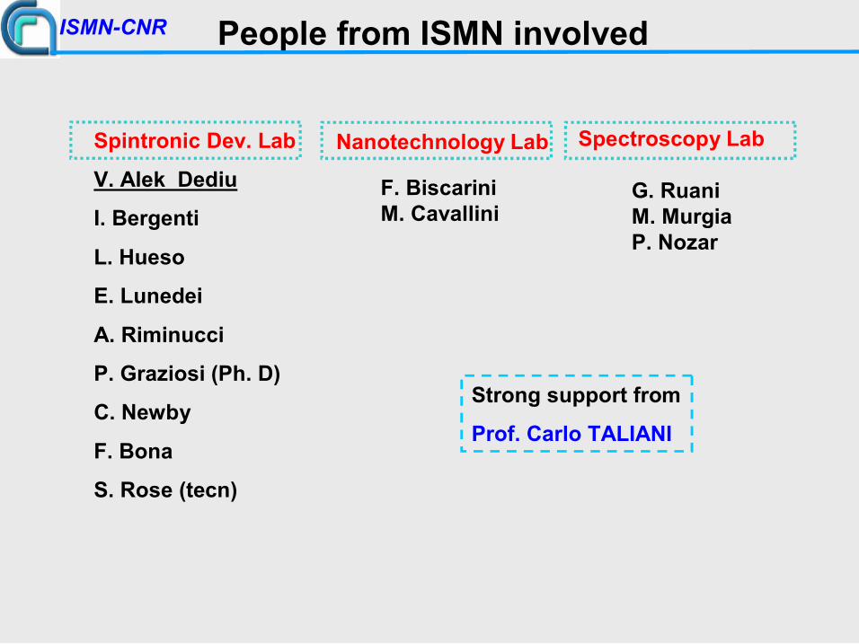
People from ISMN involved
G. Ruani M. Murgia P. Nozar
Nanotechnology Lab Spectroscopy Lab
F. Biscarini M. Cavallini
Spintronic Dev. Lab
V. Alek Dediu
I. Bergenti
L. Hueso
E. Lunedei
A. Riminucci
P. Graziosi (Ph. D)
C. Newby
F. Bona
S. Rose (tecn)
Strong support from
Prof. Carlo TALIANI
ISMNCNR
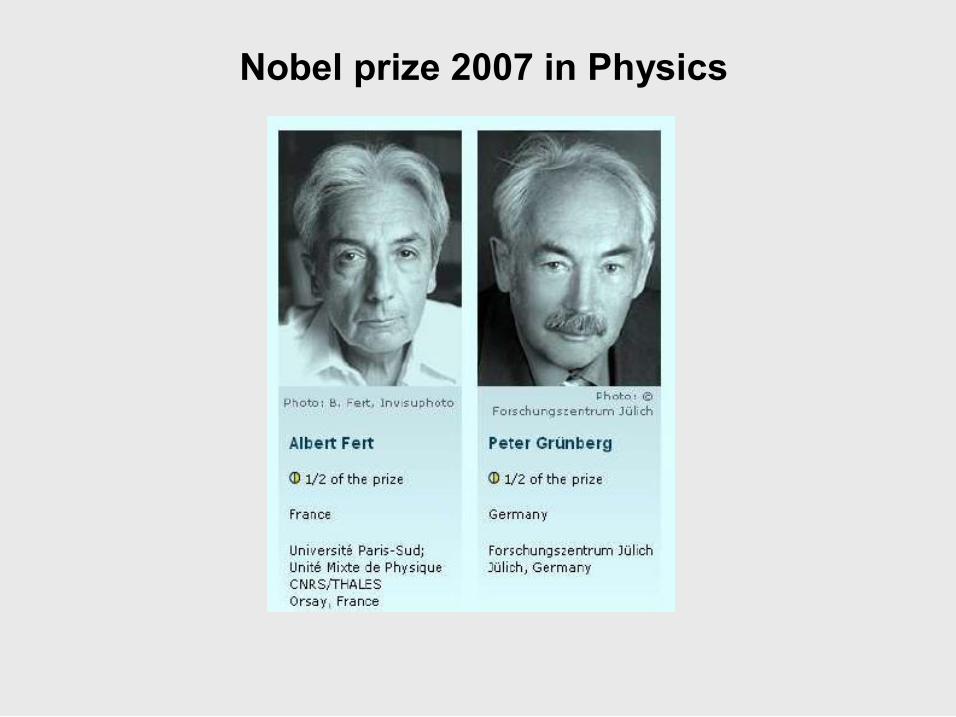
Nobel prize 2007 in Physics
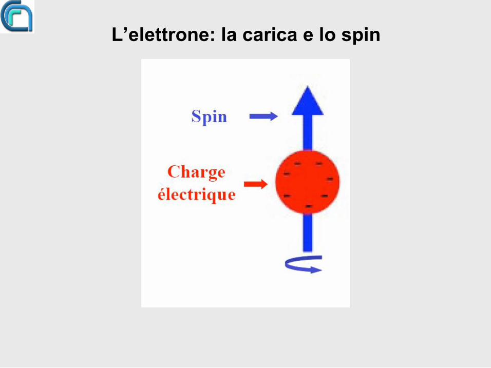
L’elettrone: la carica e lo spin
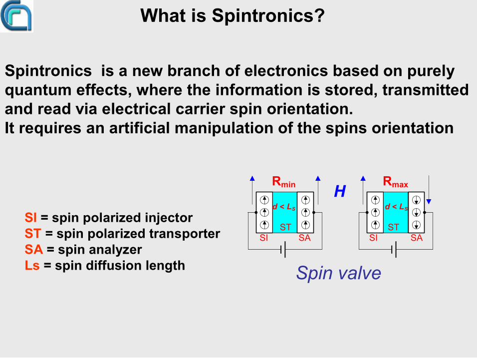
What is Spintronics?
H Rmin Rmax
d < L S d < L S
ST ST SI SA SI SA
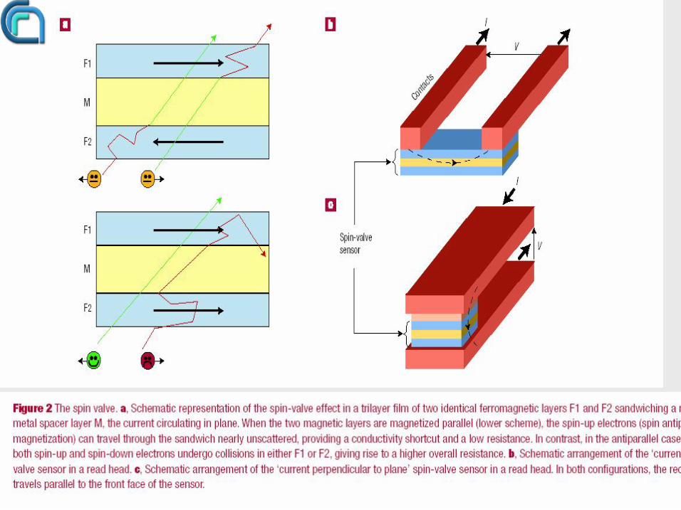
Spin valve
Spintronics is a new branch of electronics based on purely quantum effects, where the information is stored, transmitted and read via electrical carrier spin orientation. It requires an artificial manipulation of the spins orientation
SI = spin polarized injector ST = spin polarized transporter SA = spin analyzer Ls = spin diffusion length
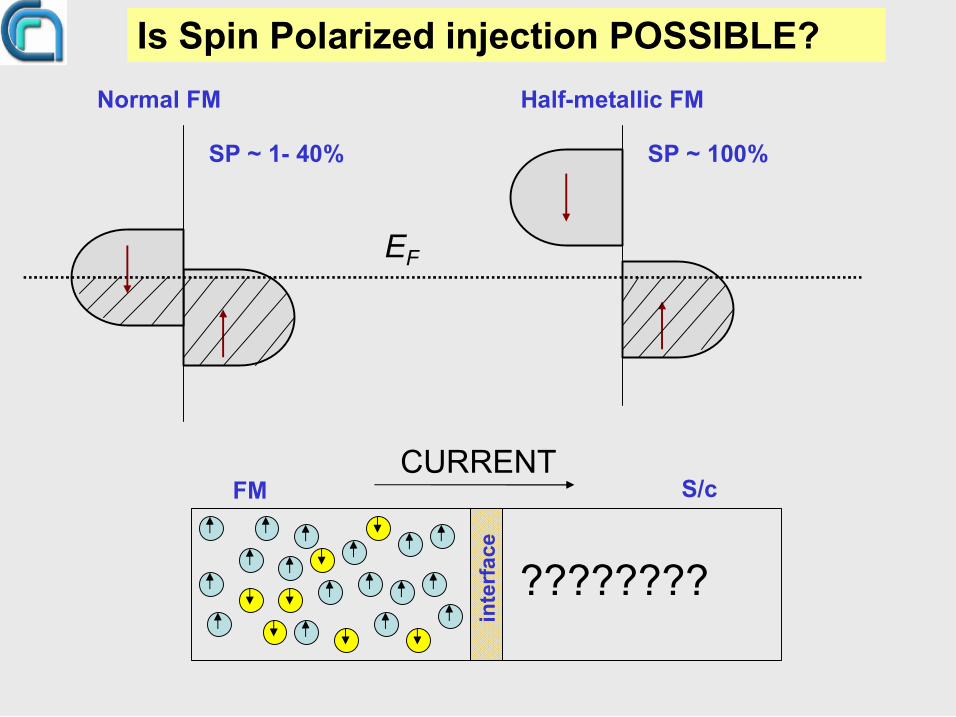
Is Spin Polarized injection POSSIBLE? Normal FM Halfmetallic FM
E F
SP ~ 1 40% SP ~ 100%
FM S/c
????????
CURRENT interface
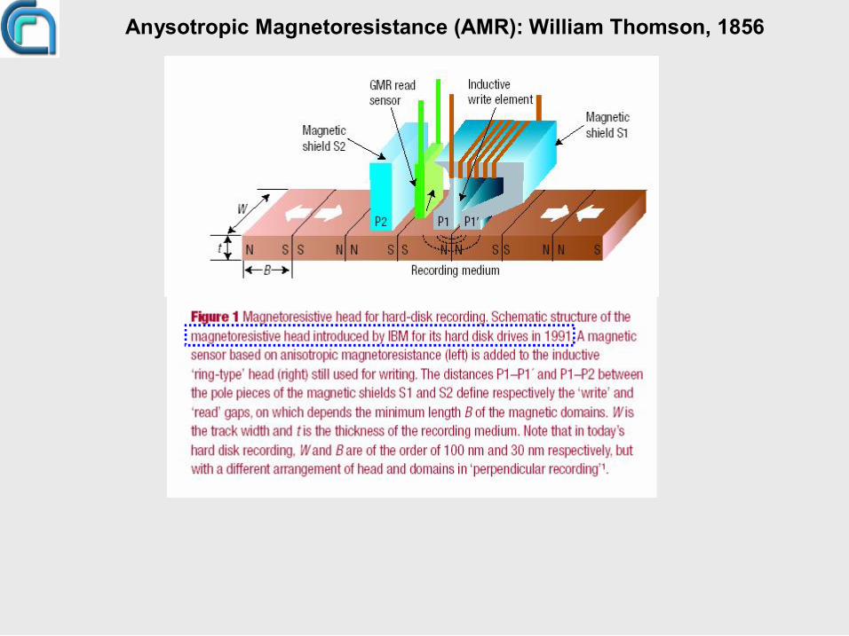
Anysotropic Magnetoresistance (AMR): William Thomson, 1856
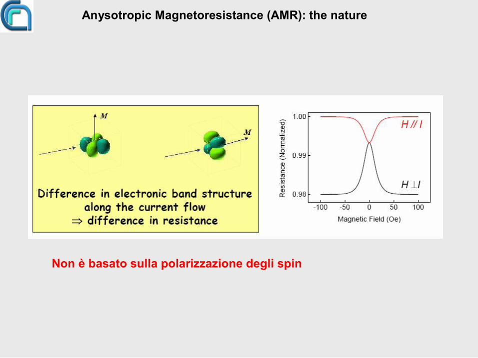
Anysotropic Magnetoresistance (AMR): the nature
Non è basato sulla polarizzazione degli spin
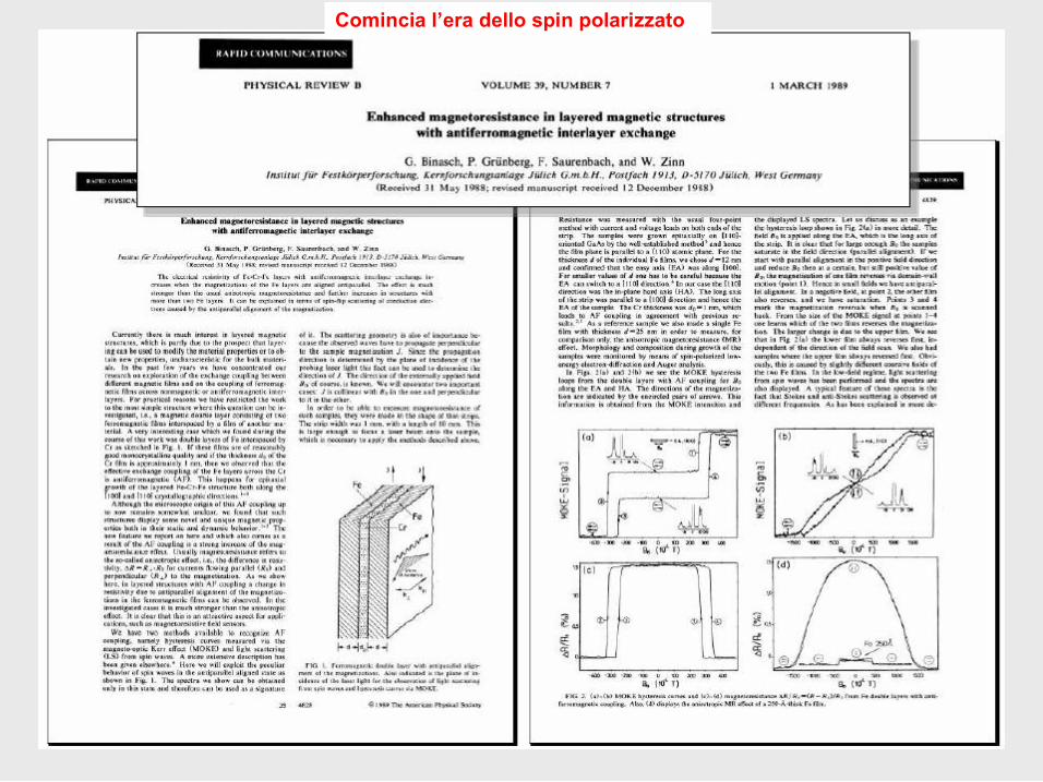
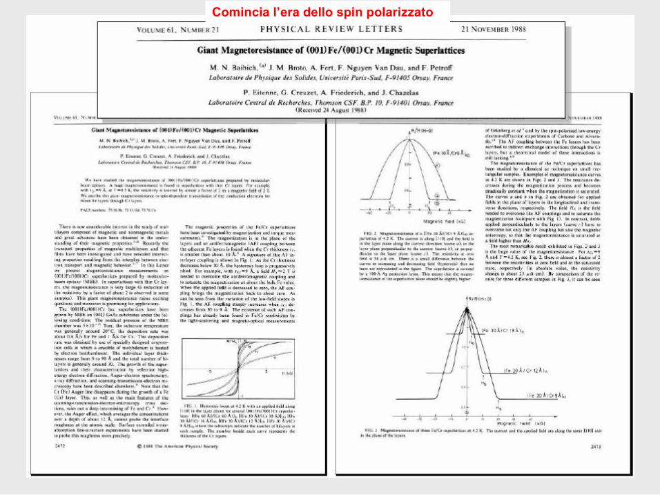
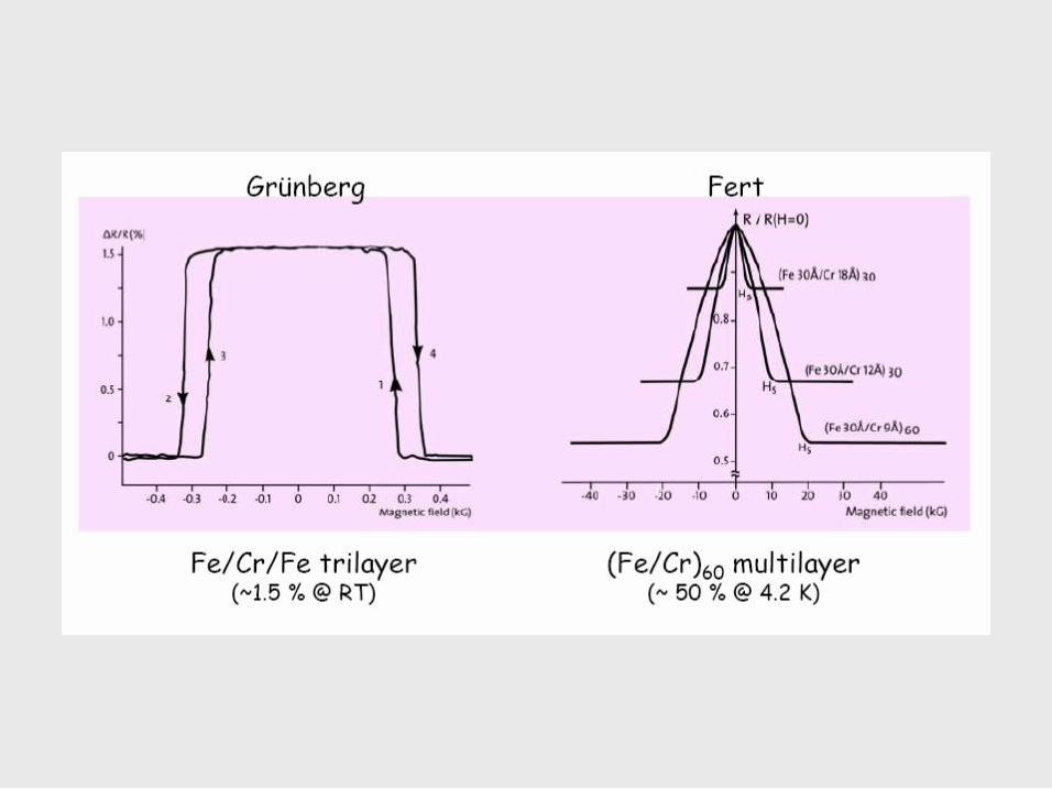
Comincia l’era dello spin polarizzato
Comincia l’era dello spin polarizzato
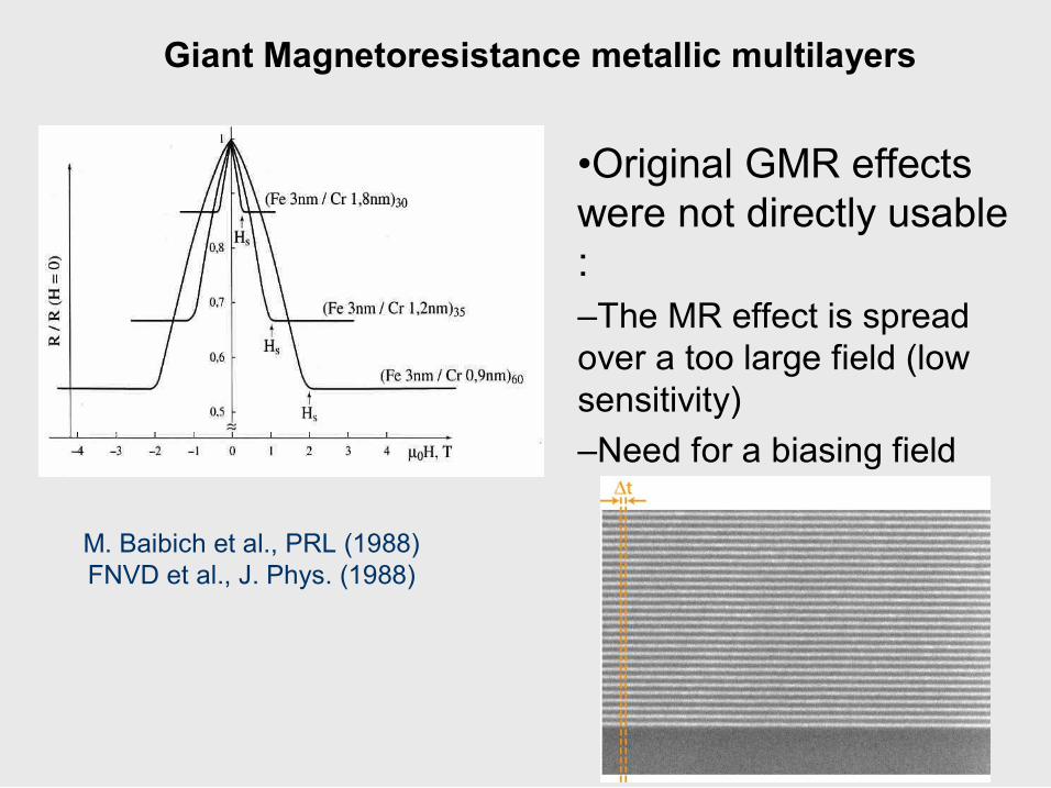
•Original GMR effects were not directly usable : –The MR effect is spread over a too large field (low sensitivity) –Need for a biasing field
M. Baibich et al., PRL (1988) FNVD et al., J. Phys. (1988)
Giant Magnetoresistance metallic multilayers
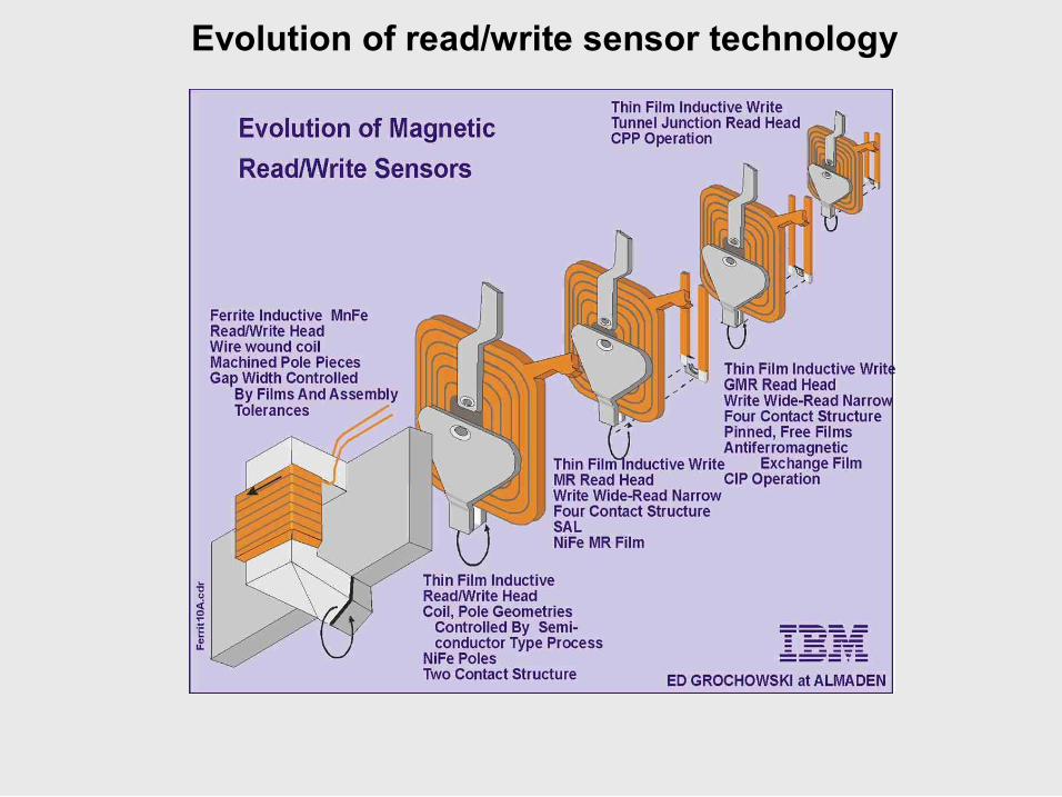
Evolution of read/write sensor technology
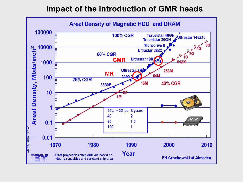
Impact of the introduction of GMR heads
MR
GMR
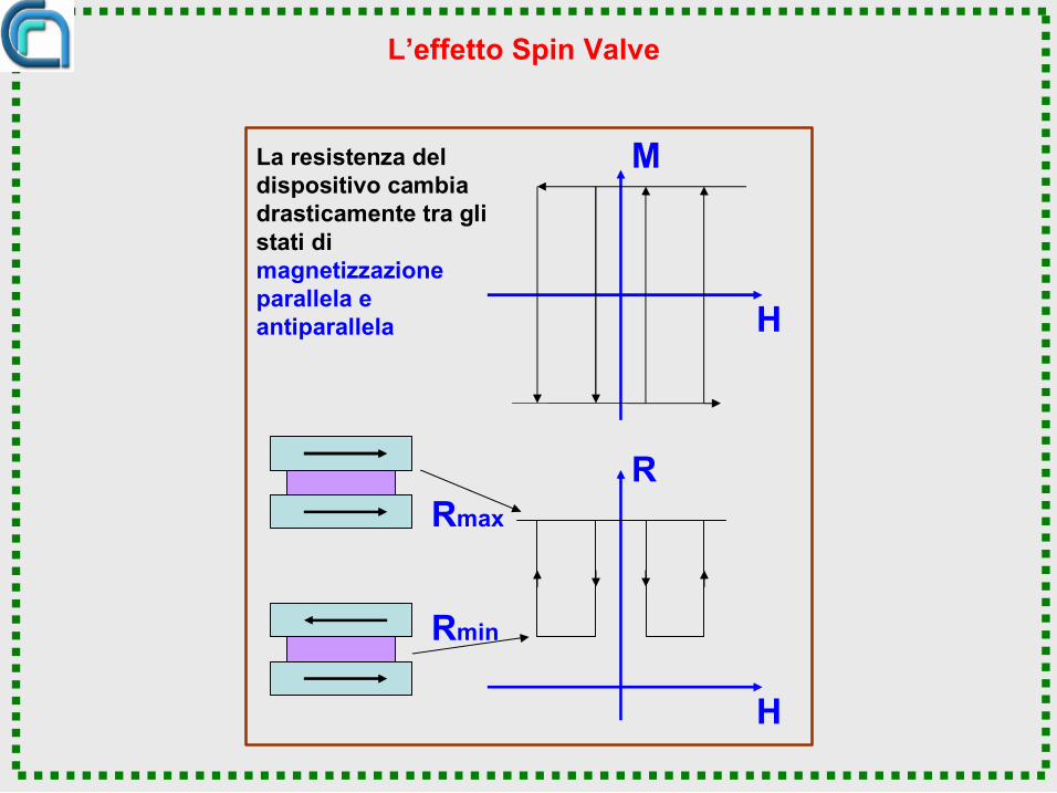
L’effetto Spin Valve
M
H
H
R
Rmin
Rmax
La resistenza del dispositivo cambia drasticamente tra gli stati di magnetizzazione parallela e antiparallela
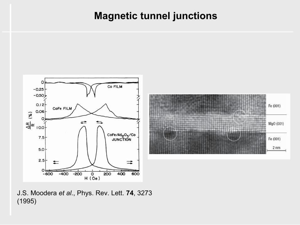
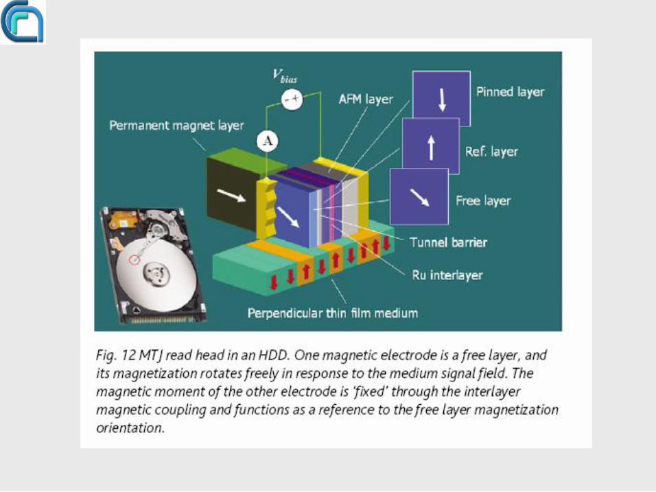
Magnetic tunnel junctions
J.S. Moodera et al., Phys. Rev. Lett. 74, 3273 (1995)
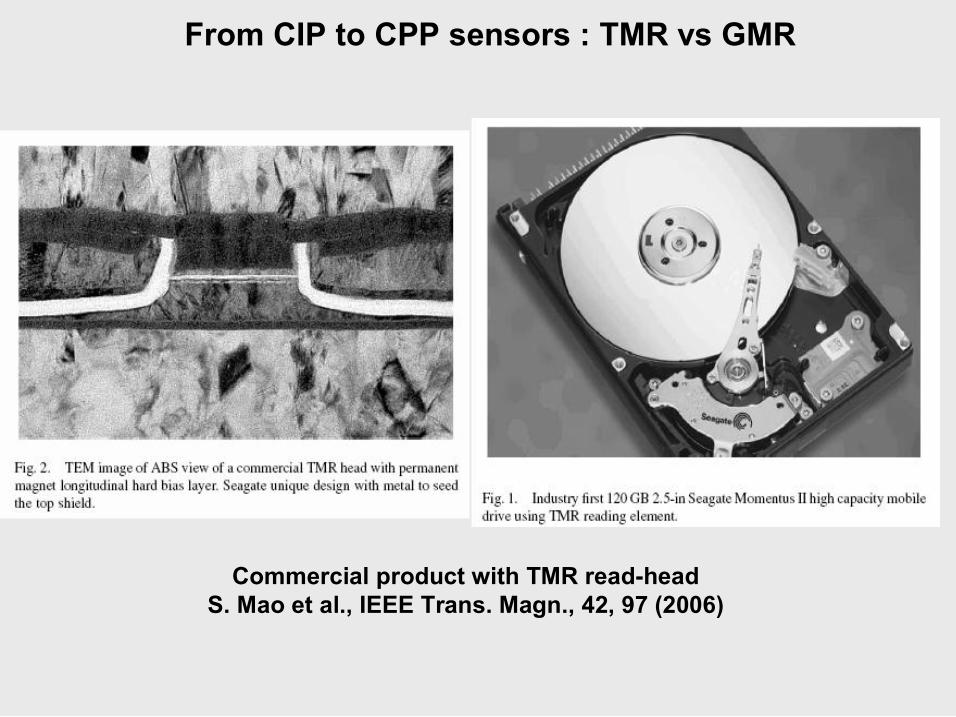
From CIP to CPP sensors : TMR vs GMR
Commercial product with TMR readhead S. Mao et al., IEEE Trans. Magn., 42, 97 (2006)
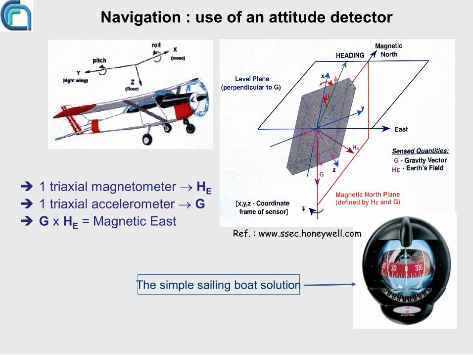
Navigation : use of an attitude detector
è 1 triaxial magnetometer → H E è 1 triaxial accelerometer → G è G x H E = Magnetic East
Ref. : www.ssec.honeywell.com
The simple sailing boat solution
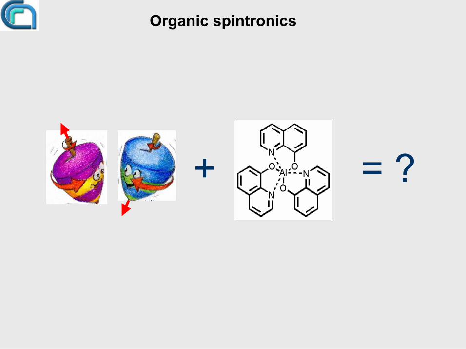
= ? +
Organic spintronics
Most organic semiconductors are characterized by very weak spin scattering strength:
low SpinOrbit Coupling (low Z values) and low Hyperfine Interaction (πconjugation)
possibility to transport the spin polarized signal to long distances (10 2 nm) even at room temperatures
Technological advantages: easy to grow, low sensitivity to impurities stable and easily controlable interfaces with many inorganic materials – interface tuning by Self Assembled Monolayers
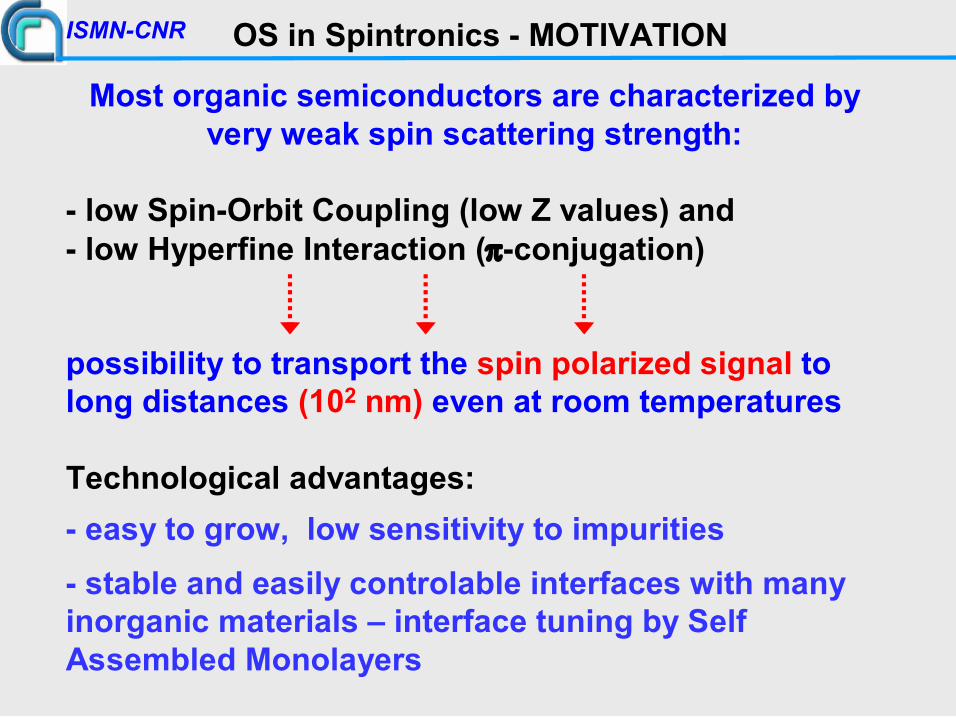
OS in Spintronics MOTIVATION ISMNCNR
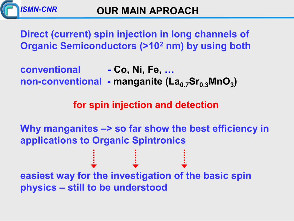
OUR MAIN APROACH ISMNCNR
Direct (current) spin injection in long channels of Organic Semiconductors (>10 2 nm) by using both
conventional Co, Ni, Fe, … nonconventional manganite (La 0.7 Sr 0.3 MnO 3 )
for spin injection and detection
Why manganites –> so far show the best efficiency in applications to Organic Spintronics
easiest way for the investigation of the basic spin physics – still to be understood
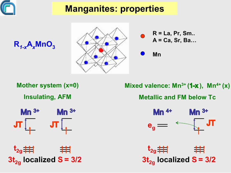
Manganites: properties
3t 2g localized S = 3/2 t 2g
e g JT
R 1x A x MnO 3
Mixed valence: Mn 3+ (1-x ), Mn 4+ (x)
Metallic and FM below Tc
Mn 4+ Mn 3+
R = La, Pr, Sm.. A = Ca, Sr, Ba…
Mn
Mother system (x=0)
Insulating, AFM
JT Mn 3+
JT Mn 3+
3t 2g localized S = 3/2 t 2g
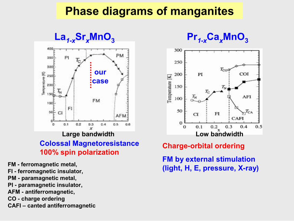
FM ferromagnetic metal, FI ferromagnetic insulator, PM paramagnetic metal, PI paramagnetic insulator, AFM antiferromagnetic, CO charge ordering CAFI – canted antiferromagnetic
Phase diagrams of manganites
La 1x Sr x MnO 3 Pr 1x Ca x MnO 3
Large bandwidth Low bandwidth Colossal Magnetoresistance 100% spin polarization
Chargeorbital ordering
FM by external stimulation (light, H, E, pressure, Xray)
our case
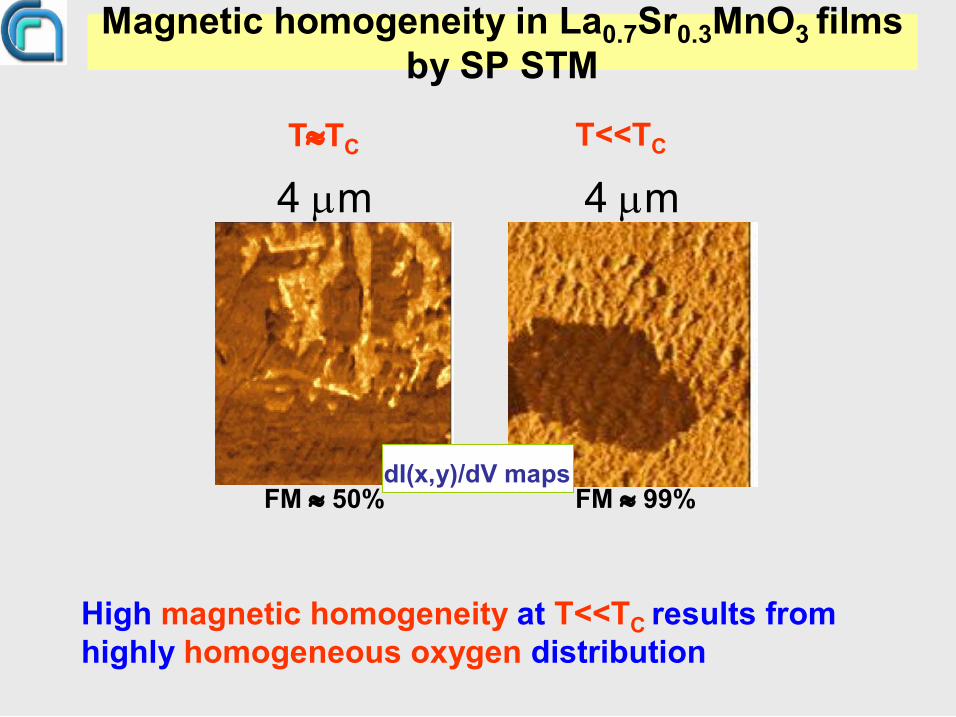
4 µm 4 µm
FM ≈ 50% dI(x,y)/dV maps
FM ≈ 99%
Magnetic homogeneity in La 0.7 Sr 0.3 MnO 3 films by SP STM
T<<T C T≈T C
High magnetic homogeneity at T<<T C results from highly homogeneous oxygen distribution
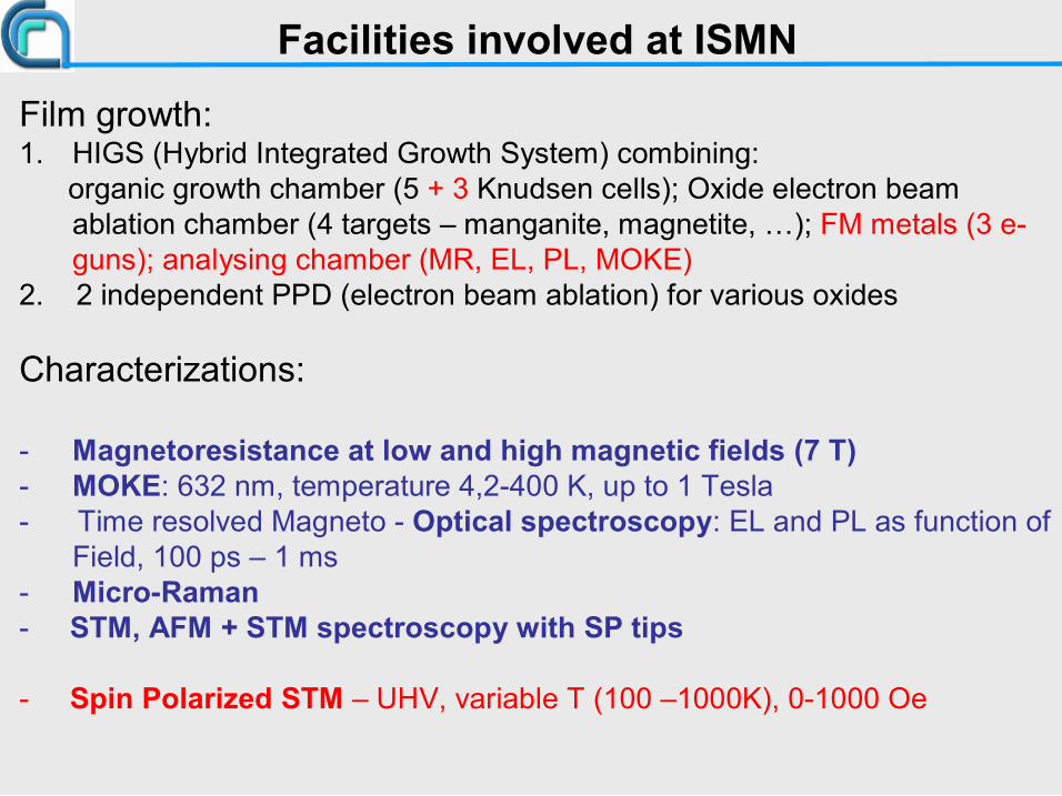
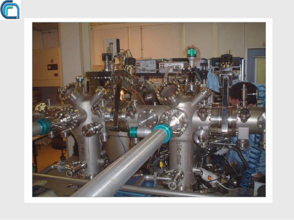
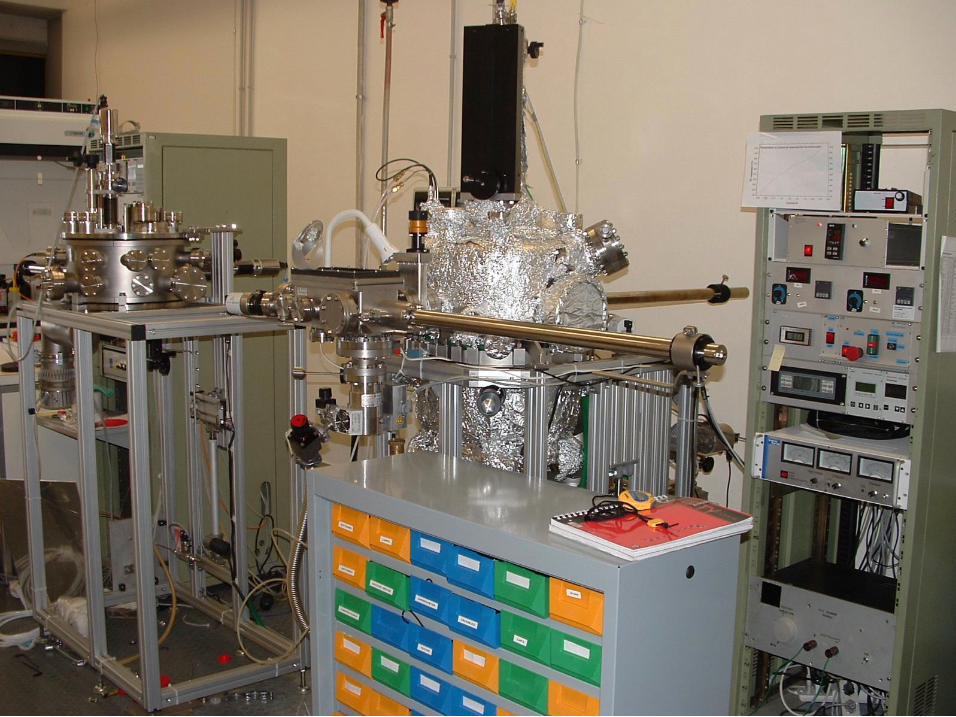
Film growth: 1. HIGS (Hybrid Integrated Growth System) combining:
organic growth chamber (5 + 3 Knudsen cells); Oxide electron beam ablation chamber (4 targets – manganite, magnetite, …); FM metals (3 e guns); analysing chamber (MR, EL, PL, MOKE)
2. 2 independent PPD (electron beam ablation) for various oxides
Characterizations:
Magnetoresistance at low and high magnetic fields (7 T) MOKE: 632 nm, temperature 4,2400 K, up to 1 Tesla Time resolved Magneto Optical spectroscopy: EL and PL as function of
Field, 100 ps – 1 ms MicroRaman STM, AFM + STM spectroscopy with SP tips
Spin Polarized STM – UHV, variable T (100 –1000K), 01000 Oe
Facilities involved at ISMN
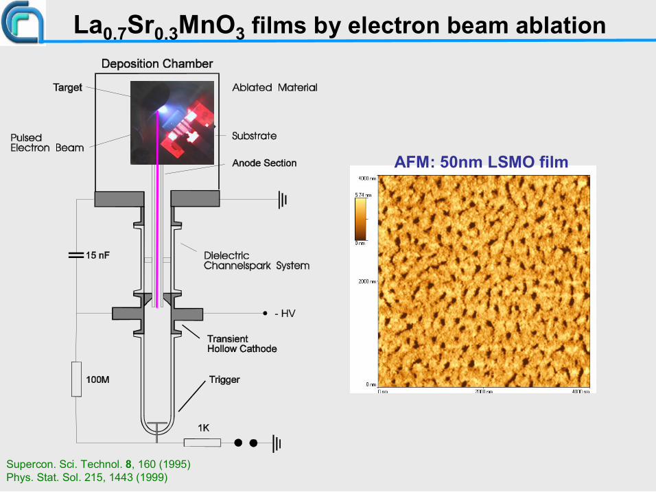
AFM: 50nm LSMO film
Supercon. Sci. Technol. 8, 160 (1995) Phys. Stat. Sol. 215, 1443 (1999)
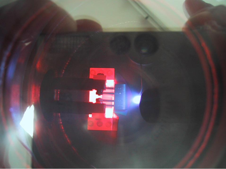
La 0.7 Sr 0.3 MnO 3 films by electron beam ablation
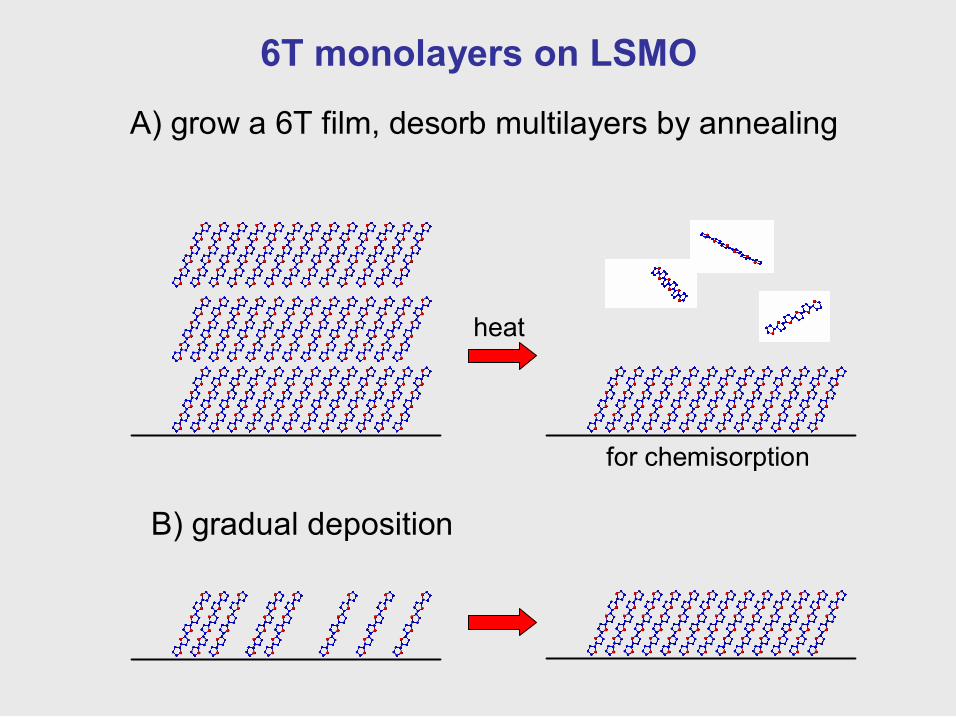
6T monolayers on LSMO
A) grow a 6T film, desorb multilayers by annealing
B) gradual deposition
for chemisorption
heat
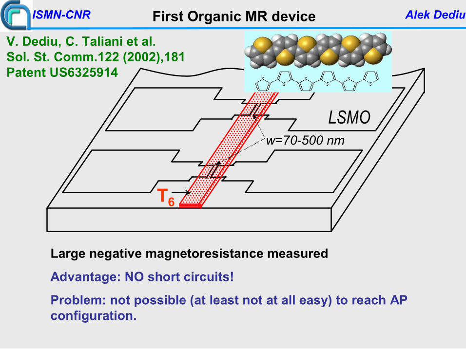
T 6
LSMO w=70500 nm
V. Dediu, C. Taliani et al. Sol. St. Comm.122 (2002),181 Patent US6325914
Large negative magnetoresistance measured
Advantage: NO short circuits!
Problem: not possible (at least not at all easy) to reach AP configuration.
First Organic MR device ISMNCNR Alek Dediu
w=200 nm w=400 nm
0,0 0,1 0,2 0,3 0,00
0,05
0,10
w=140 nm
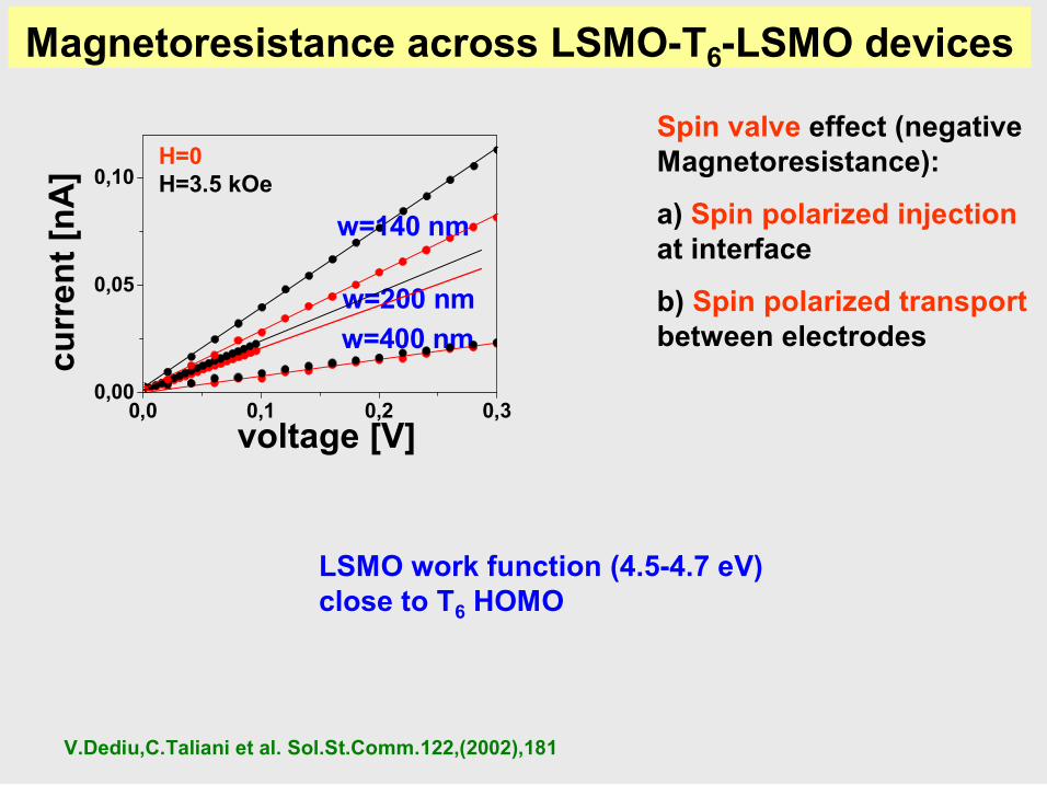
Magnetoresistance across LSMOT 6 LSMO devices
H=0 H=3.5 kOe
Spin valve effect (negative Magnetoresistance):
a) Spin polarized injection at interface
b) Spin polarized transport between electrodes
V.Dediu,C.Taliani et al. Sol.St.Comm.122,(2002),181
curren
t [nA
]
voltage [V]
LSMO work function (4.54.7 eV) close to T 6 HOMO
100 200 300 400 500
0.0
0.2
0.4
0.6
0.8
1.0
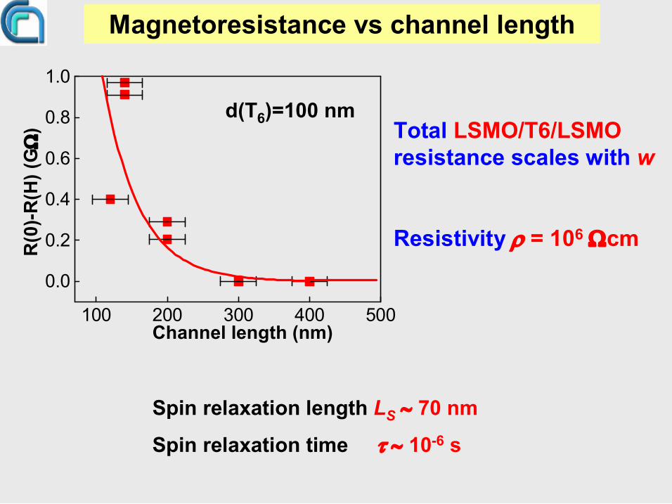
Magnetoresistance vs channel length
Channel length (nm)
R(0)R
(H) (G
Ω) Total LSMO/T6/LSMO resistance scales with w
Resistivity ρ = 10 6 Ωcm
d(T 6 )=100 nm
Spin relaxation length L S ∼ 70 nm
Spin relaxation time τ ∼ 10 6 s
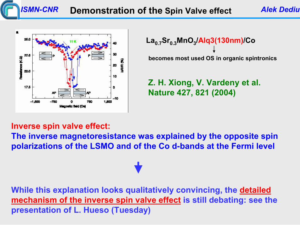
Z. H. Xiong, V. Vardeny et al. Nature 427, 821 (2004)
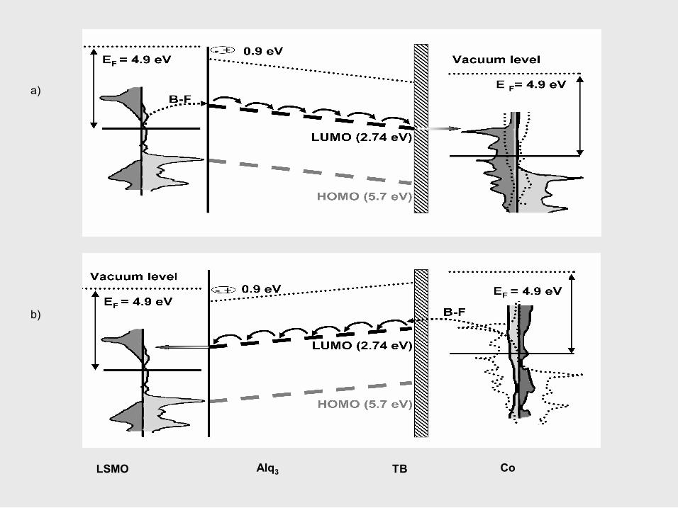
La 0.7 Sr 0.3 MnO 3 /Alq3(130nm)/Co
Inverse spin valve effect: The inverse magnetoresistance was explained by the opposite spin polarizations of the LSMO and of the Co dbands at the Fermi level
Demonstration of the Spin Valve effect ISMNCNR Alek Dediu
While this explanation looks qualitatively convincing, the detailed mechanism of the inverse spin valve effect is still debating: see the presentation of L. Hueso (Tuesday)
becomes most used OS in organic spintronics
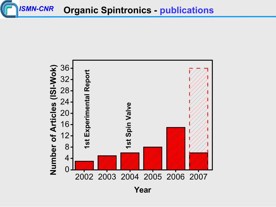
2002 2003 2004 2005 2006 2007 0 4 8 12 16 20 24 28 32 36
Num
ber o
f Articles (IS
IWok
)
Year
Organic Spintronics publications ISMNCNR
1st E
xperim
ental R
eport
1st S
pin Va
lve
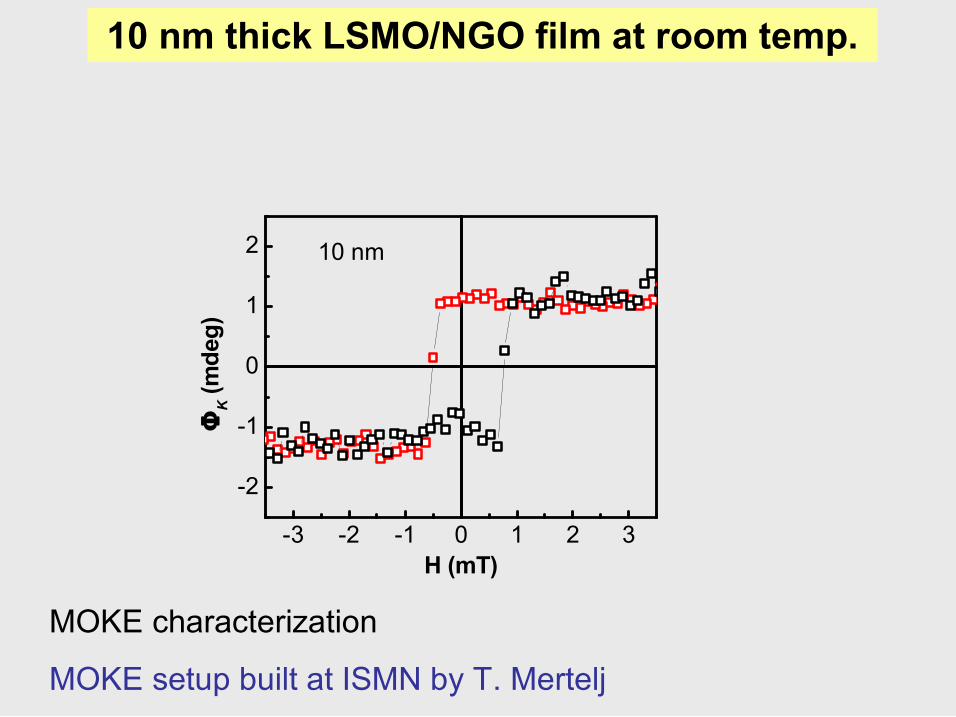
3 2 1 0 1 2 3
2
1
0
1
2 10 nm
Φ K (m
deg)
H (mT)
10 nm thick LSMO/NGO film at room temp.
MOKE characterization
MOKE setup built at ISMN by T. Mertelj
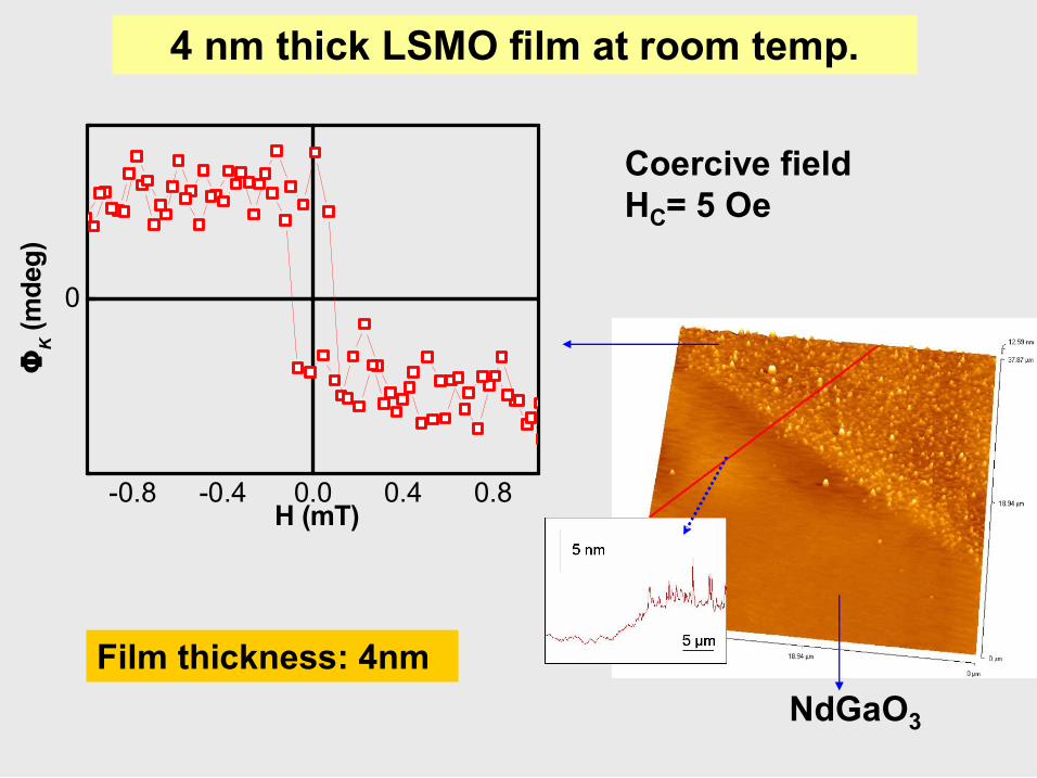
4 nm thick LSMO film at room temp.
Film thickness: 4nm
Coercive field H C = 5 Oe
NdGaO 3
0.8 0.4 0.0 0.4 0.8
0
Φ K (m
deg)
H (mT)
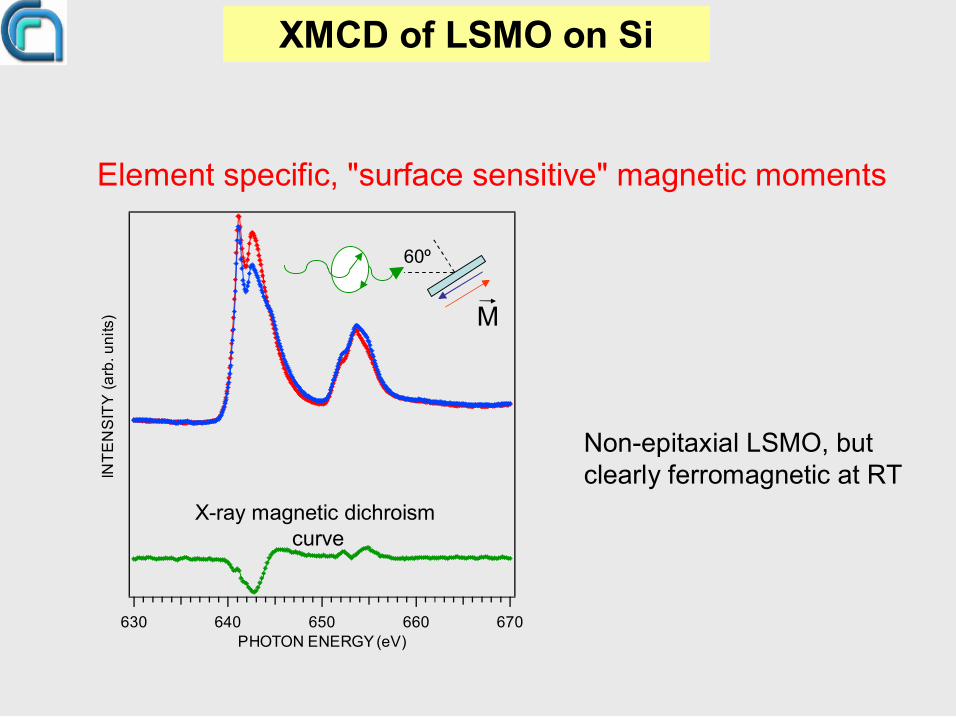
INTE
NSITY (arb. units)
670 660 650 640 630 PHOTON ENERGY (eV)
60º
M
Xray magnetic dichroism curve
Nonepitaxial LSMO, but clearly ferromagnetic at RT
Element specific, "surface sensitive" magnetic moments
XMCD of LSMO on Si
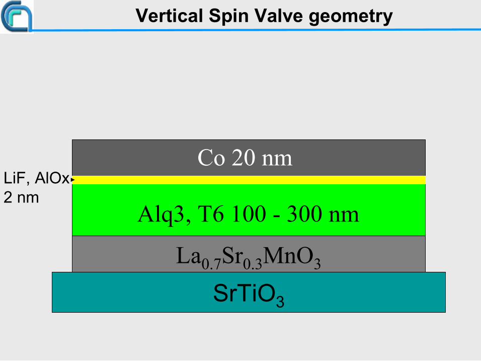
SrTiO 3
La 0.7 Sr 0.3 MnO 3
Alq3, T6 100 300 nm
Co 20 nm LiF, AlOx 2 nm
Vertical Spin Valve geometry
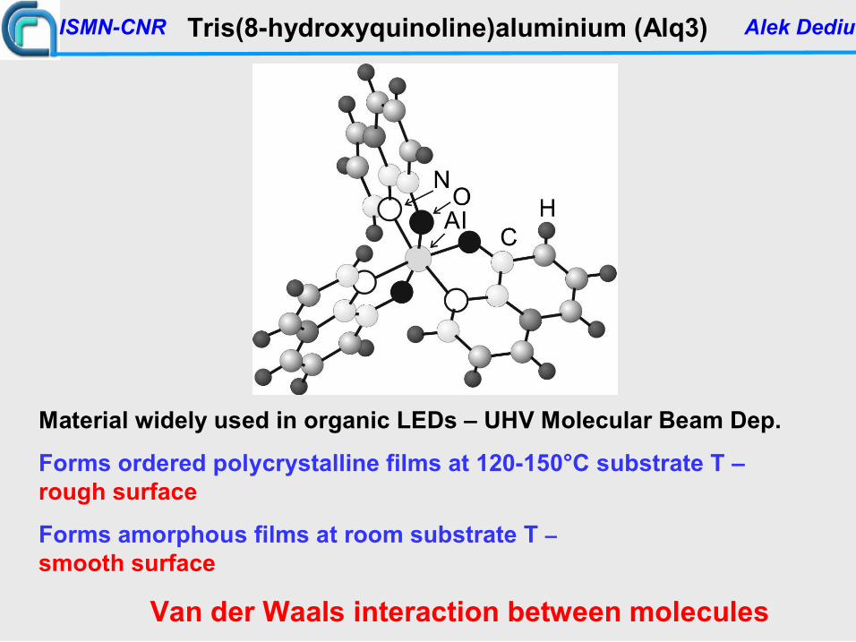
Tris(8hydroxyquinoline)aluminium (Alq3) ISMNCNR
Material widely used in organic LEDs – UHV Molecular Beam Dep.
Forms ordered polycrystalline films at 120150°C substrate T – rough surface
Forms amorphous films at room substrate T – smooth surface
Van der Waals interaction between molecules
Alek Dediu
1.0 0.5 0.0 0.5 1.0
150
0
150
300 I (
µA)
Voltage (V)
LSMO/Alq3(80 nm)/Al 2 O
3 /Co
RT 100 K
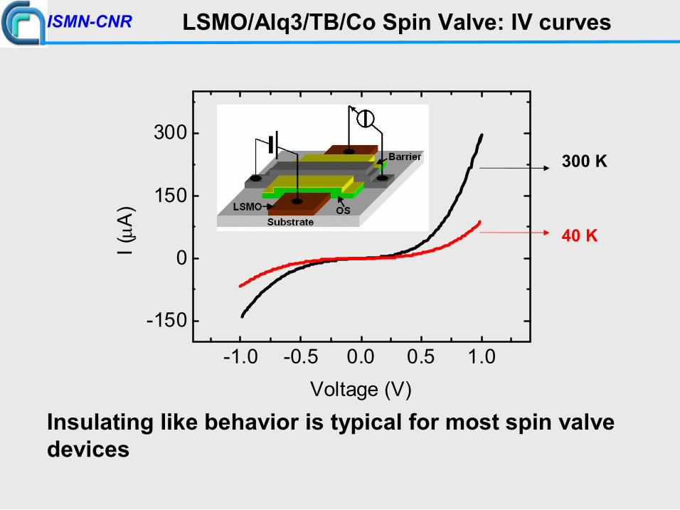
Insulating like behavior is typical for most spin valve devices
LSMO/Alq3/TB/Co Spin Valve: IV curves
300 K
40 K
ISMNCNR
80 40 0 40 80
0.15
0.10
0.05
0.00
500 250 0 250 500 12
8
4
0
0 100 200 300 0
4
8
12
Magnetic Field (Oe)
MR(%
)
MR(%
)
Magnetic Field (Oe) Temperature (K)
MR (%
)
100 200 300 0 5 10 15
MR (%
)
Alq 3 t (nm)
80 40 0 40 80 2
1
0
1
2
0 5 10 15 20
MOKE (a.u.)
Magnetic Field (Oe)
Reflectivity
(a.u.)
Angle (deg)
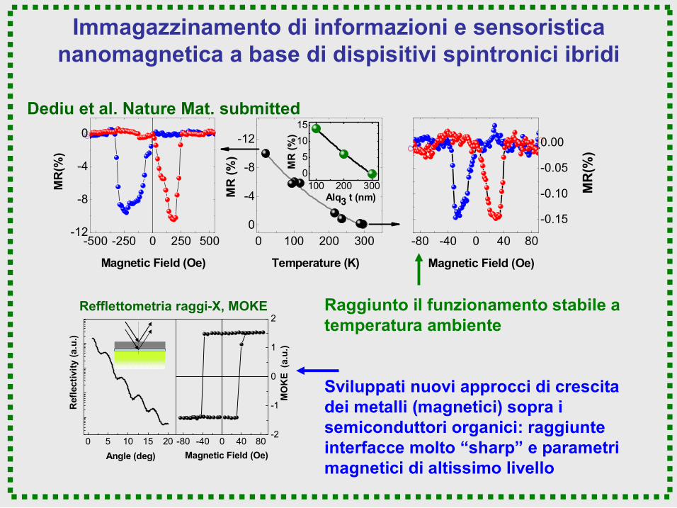
Immagazzinamento di informazioni e sensoristica nanomagnetica a base di dispisitivi spintronici ibridi
Dediu et al. Nature Mat. submitted
Raggiunto il funzionamento stabile a temperatura ambiente
Sviluppati nuovi approcci di crescita dei metalli (magnetici) sopra i semiconduttori organici: raggiunte interfacce molto “sharp” e parametri magnetici di altissimo livello
Refflettometria raggiX, MOKE
a)
b)
LSMO Alq 3 TB Co
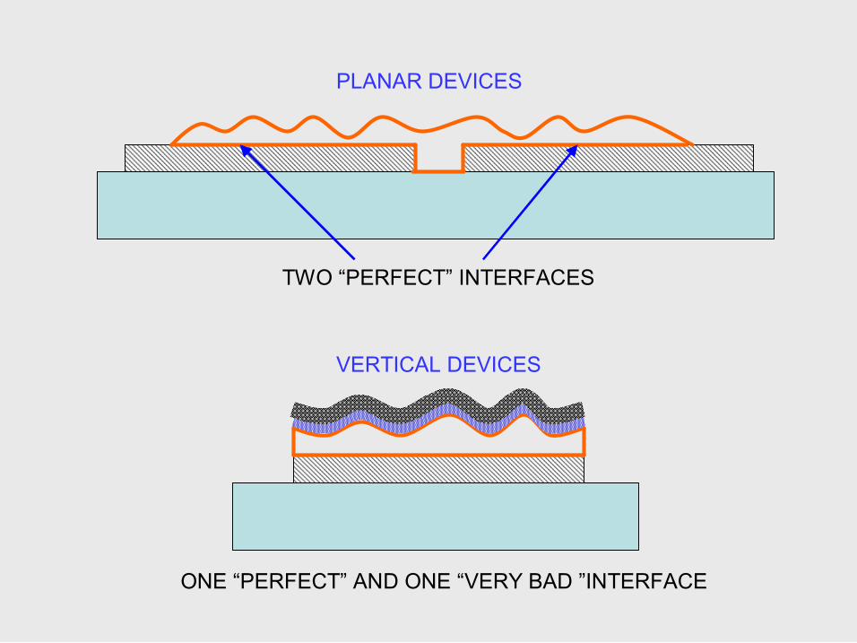
PLANAR DEVICES
TWO “PERFECT” INTERFACES
VERTICAL DEVICES
ONE “PERFECT” AND ONE “VERY BAD ”INTERFACE
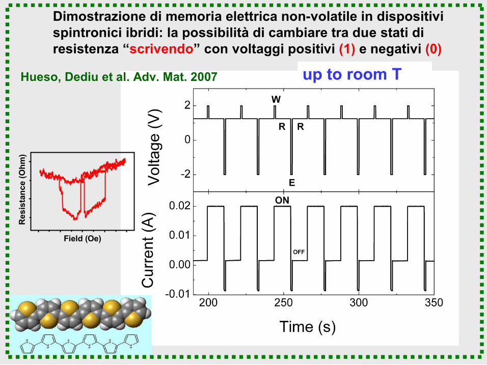
Dimostrazione di memoria elettrica nonvolatile in dispositivi spintronici ibridi: la possibilità di cambiare tra due stati di resistenza “scrivendo” con voltaggi positivi (1) e negativi (0)
up to room T Hueso, Dediu et al. Adv. Mat. 2007
Resistanc
e (Ohm
)
Field (Oe)
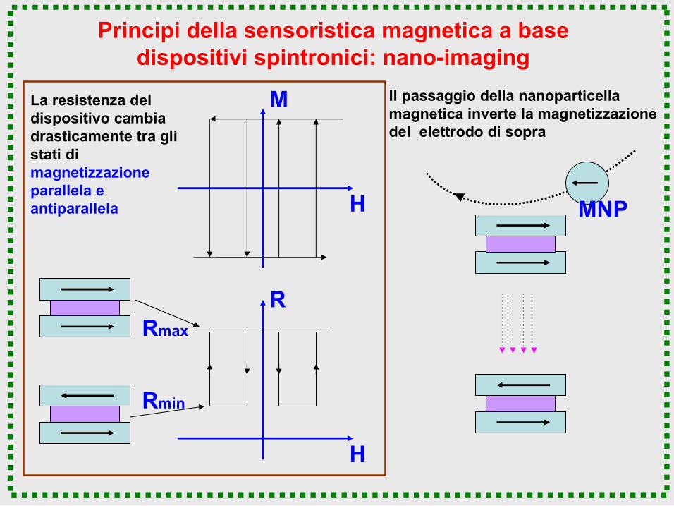
Principi della sensoristica magnetica a base dispositivi spintronici: nanoimaging
M
H
H
R
Rmin
Rmax
MNP
Il passaggio della nanoparticella magnetica inverte la magnetizzazione del elettrodo di sopra
La resistenza del dispositivo cambia drasticamente tra gli stati di magnetizzazione parallela e antiparallela
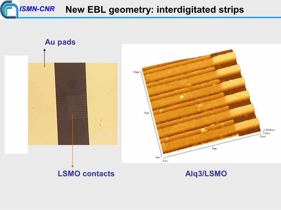
New EBL geometry: interdigitated strips
Au pads
Alq3/LSMO LSMO contacts
ISMNCNR
SPECTROMETER
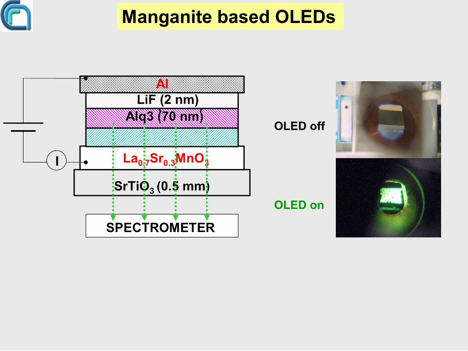
SrTiO 3 (0.5 mm)
La 0.7 Sr 0.3 MnO 3
TPD (70 nm) Alq3 (70 nm)
I
LiF (2 nm)
Manganite based OLEDs
Al
OLED off
OLED on
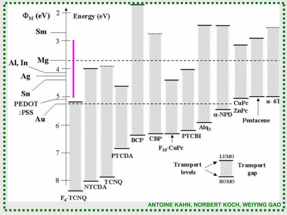
ANTOINE KAHN, NORBERT KOCH, WEIYING GAO
400 600 800
0.2
0.4
0.6
0.8
1.0
30 nm
90 nm 40 nm
12 nm
Transm
ittance
wavelenght (nm)
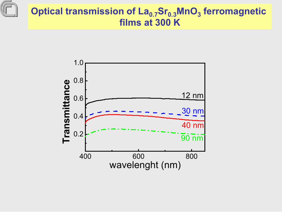
Optical transmission of La 0.7 Sr 0.3 MnO 3 ferromagnetic films at 300 K
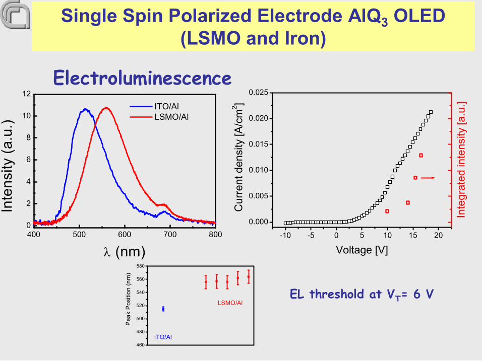
460
480
500
520
540
560
580
LSMO/Al
ITO/Al
Peak Position (n
m)
Single Spin Polarized Electrode AlQ 3 OLED (LSMO and Iron)
EL threshold at V T = 6 V
Electroluminescence
400 500 600 700 800 0
2
4
6
8
10
12
Intensity (a
.u.)
λ (nm)
ITO/Al LSMO/Al
10 5 0 5 10 15 20
0.000
0.005
0.010
0.015
0.020
0.025
Integrated intensity [a.u.]
Current density [A
/cm 2 ]
Voltage [V]
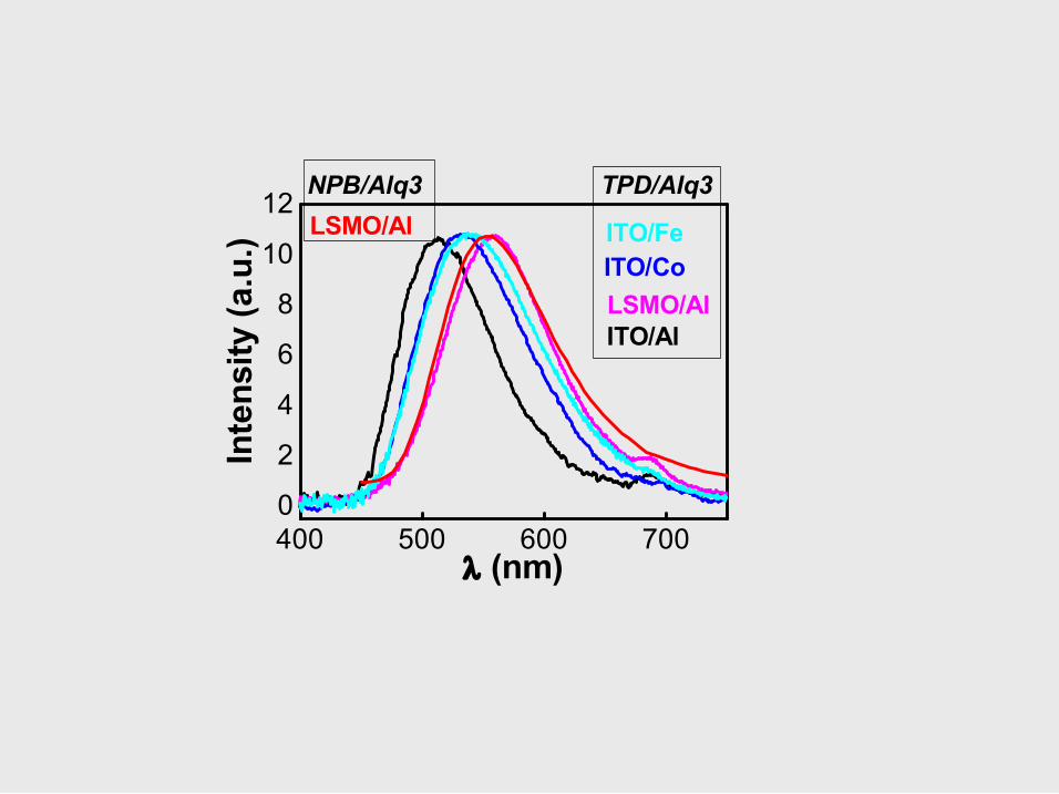
400 500 600 700 0
2
4
6
8
10
12 TPD/Alq3 NPB/Alq3 LSMO/Al ITO/Fe
ITO/Co LSMO/Al ITO/Al
Intensity (a.u.)
λ (nm)

Tris(8hydroxyquinoline)aluminium (Alq3) ISMNCNR
Material widely used in organic LEDs – UHV Molecular Beam Dep.
Forms ordered polycrystalline films at 120150°C substrate T – rough surface
Forms amorphous films at room substrate T – smooth surface
Van der Waals interaction between molecules
Alek Dediu
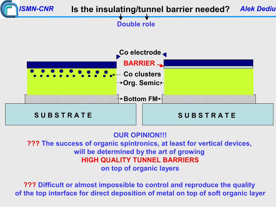
Bottom FM
Org. Semic. Co clusters
Co electrode
Is the insulating/tunnel barrier needed? ISMNCNR
OUR OPINION!!! ??? The success of organic spintronics, at least for vertical devices,
will be determined by the art of growing HIGH QUALITY TUNNEL BARRIERS
on top of organic layers
??? Difficult or almost impossible to control and reproduce the quality of the top interface for direct deposition of metal on top of soft organic layer
BARRIER
Double role
S U B S T R A T E S U B S T R A T E
Alek Dediu
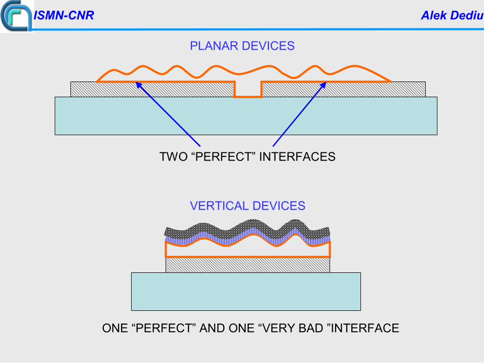
PLANAR DEVICES
TWO “PERFECT” INTERFACES
VERTICAL DEVICES
ONE “PERFECT” AND ONE “VERY BAD ”INTERFACE
ISMNCNR Alek Dediu
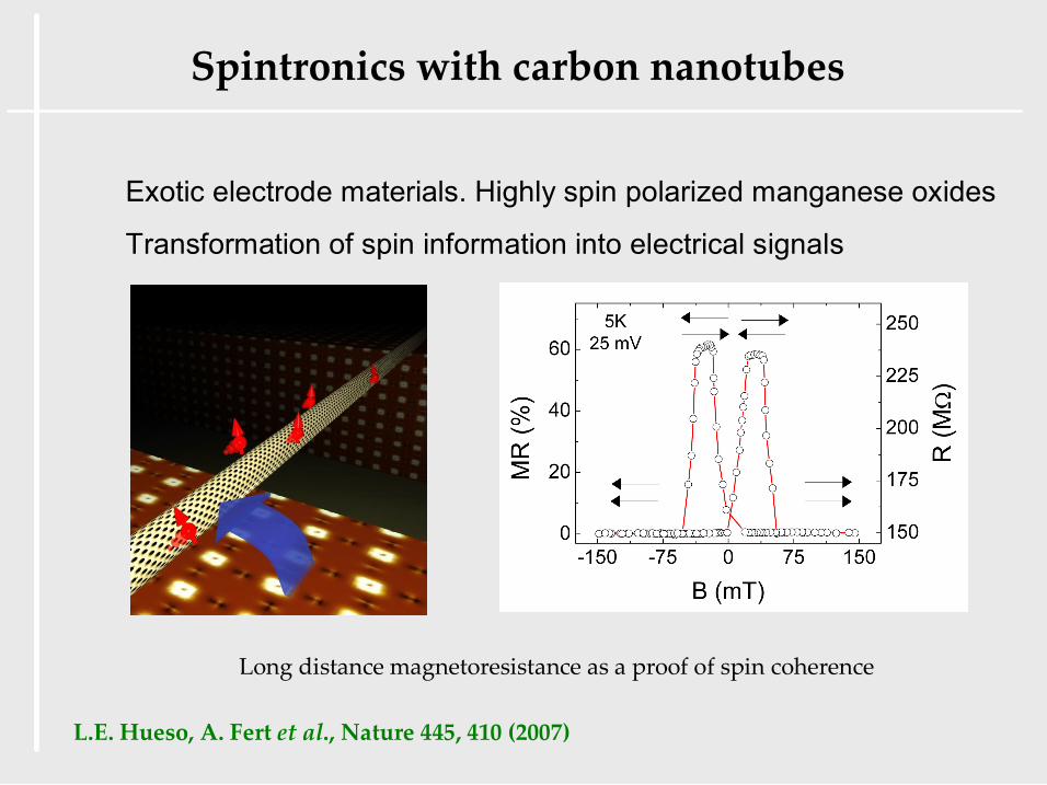
Exotic electrode materials. Highly spin polarized manganese oxides
Transformation of spin information into electrical signals
Spintronics with carbon nanotubes
L.E. Hueso, A. Fert et al., Nature 445, 410 (2007)
Long distance magnetoresistance as a proof of spin coherence
ISMNCNR Alek Dediu
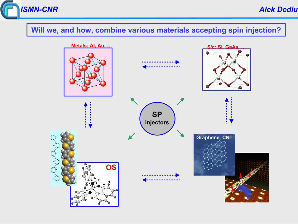
Graphene, CNT
OS
S/c: Si, GaAs, … Metals: Al, Au, …
Will we, and how, combine various materials accepting spin injection?
SP injectors
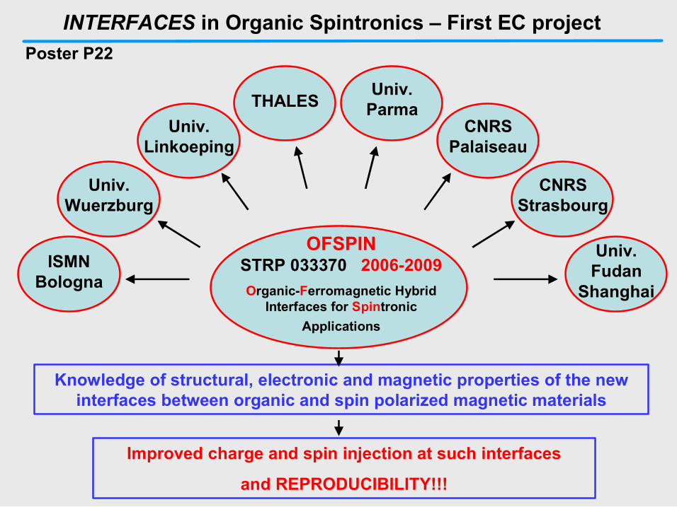
INTERFACES in Organic Spintronics – First EC project Poster P22
OFSPIN STRP 033370 20062009 OrganicFerromagnetic Hybrid
Interfaces for Spintronic Applications
ISMN Bologna
Univ. Linkoeping
Univ. Wuerzburg
Univ. Parma
Univ. Fudan
Shanghai
CNRS Strasbourg
CNRS Palaiseau
THALES
Knowledge of structural, electronic and magnetic properties of the new interfaces between organic and spin polarized magnetic materials
Improved charge and spin injection at such interfaces
and REPRODUCIBILITY!!!
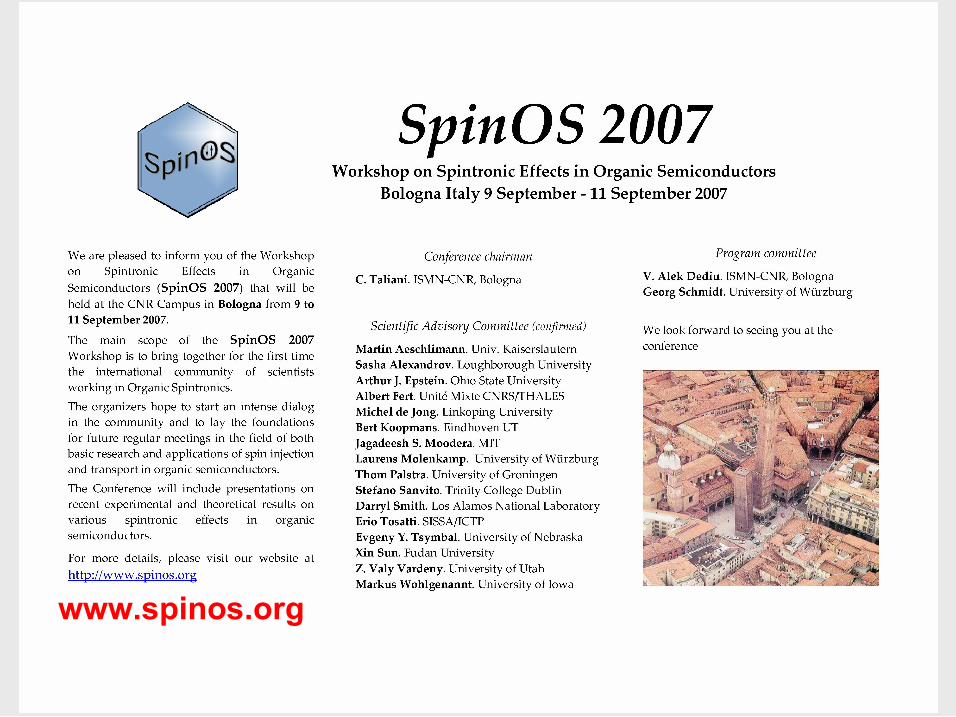
www.spinos.org


![Benutzerhinweise Useful Information - Edition · PDF fileAcuña, Luis Gustavo Caprichos Iberoamericanos [ % ] em 1016 [2-3], 8 Pages ISMN M-2032-0014-7 € 6,80 Tríptico em 1011 Homenaje](https://img.pdfslide.org/doc/110x75/5a812a067f8b9aee018d019b/benutzerhinweise-useful-information-edition-luis-gustavo-caprichos-iberoamericanos.jpg)