Embed Size (px)
Citation preview
Research ArticleSynthesis of GeSe
2Nanobelts Using Thermal Evaporation and
Their Photoelectrical Properties
Lijie Zhang,1,2 Hongfei Yu,2 Yun Yang,2 Keqin Yang,2 Youqing Dong,2 Shaoming Huang,2
Ning Dai,1 and Da-Ming Zhu1,3
1 National Laboratory for Infrared Physics, Shanghai Institute of Technical Physics, Chinese Academy of Sciences,Shanghai 200083, China
2Nanomaterials and Chemistry Key Laboratory, Wenzhou University, Wenzhou 325027, China3University of Missouri-Kansas City, Kansas City, MO 64110, USA
Correspondence should be addressed to Da-Ming Zhu; [email protected]
Received 12 March 2014; Accepted 14 April 2014; Published 17 June 2014
Academic Editor: Li Li
Copyright © 2014 Lijie Zhang et al. This is an open access article distributed under the Creative Commons Attribution License,which permits unrestricted use, distribution, and reproduction in any medium, provided the original work is properly cited.
GeSe2nanobelts were synthesized via a simple thermal-evaporation process by using gold particles as catalyst and GeSe
2flakes
as starting materials. The morphology, crystal structure, and composition were characterized with scanning electron microscopy(SEM), high-resolution transmission electron microscopy (TEM), X-ray diffraction spectroscopy (XRD), X-ray photoelectronspectroscopy (XPS), and energy-dispersive X-ray spectroscopy (EDS). SEM micrographs show that most of GeSe
2nanobelts have
distinct segmented structures (wide belt, zigzag belt, and narrow belt). A possible mechanism was proposed for the growth ofsegmented nanobelts. It is possible that the growth of the segmented nanobelts is dominated by both vapor-liquid-solid andvapor-solid mechanisms. Devices made of single GeSe
2nanobelt have been fabricated and their photoelectrical property has been
investigated. Results indicate that these nanobelt devices are potential building blocks for optoelectronic applications.
1. Introduction
Recently, one-dimensional semiconductor nanostructures,such as nanowires and nanobelts or nanoribbons, haveattracted much attention because of their excellent physicalproperties and their unique structure for device applications[1]. They are considered to be excellent building blocks fordevices such as field effect transistors [2], field emitters [3–5], photodetectors [6–8], solar cells [9–11], nanolasers [12],and chemical [13] and biological sensors [14]. These devicesdemonstrate improved features in comparison to those usingbulk materials. For instance, photodetectors fabricated usingnanowire or nanobelt always exhibit high sensitivity to lightbecause of their high ratio of surface to volume [8].
IV–VI chalcogenides with layered crystal structure havebeen widely employed in construction of devices used inoptics, thermoelectrics, and optoelectronics [15–17]. As animportant member of IV–VI semiconductors, GeSe
2with
a wide band gap (∼2.7 eV) was found to have promisingapplications in electronics, optoelectronics, and renewableenergy devices [18]. Therefore, much attention has beendrawn towards the preparation and the study of prop-erty of GeSe
2nanostructures (nanowires, nanobelts, etc.).
For instance, three-dimensional GeSe2nanostructures com-
posed of nanobelts were synthesized with chemical vapordeposition (CVD) and have demonstrated very impressiveperformance in supercapacitor applications [15, 18]. GeSe
2
nanowires also could be synthesized through decomposingorganic ammonium precursor [19]. Stepped-surfaced GeSe
2
nanobelts were obtained via CVD process and showed highphotoresponsivity and gain [20]. Single GeSe
2nanobelt two-
terminal device exhibited high electronic transport prop-erties, photoconductive characteristics, and temperature-dependent electronic characteristics [21].
In most cases, one-dimensional GeSe2nanostructures
were synthesized via a wet-chemical routine or CVD process
Hindawi Publishing CorporationJournal of NanomaterialsVolume 2014, Article ID 310716, 9 pageshttp://dx.doi.org/10.1155/2014/310716
2 Journal of Nanomaterials
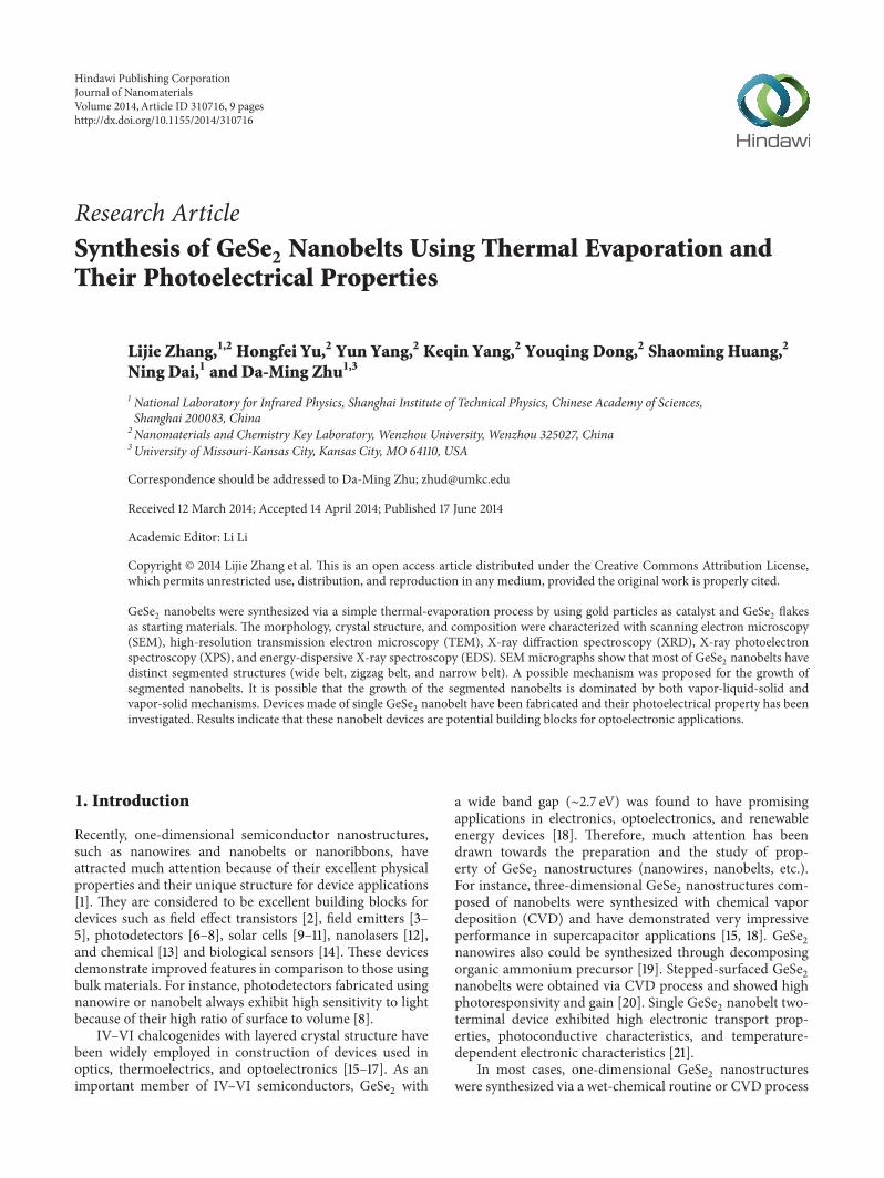
Argon flow
GeSe2∼650∘C
Si substrate450∘C
Figure 1: Schematic diagram of the synthesis of GeSe2nanobelts.
by using Ge and Se powders as starting materials [15, 18–20]. It is also known that both GeSe and GeSe
2have high
stability [17, 18]. As a result, both GeSe and GeSe2phases
probably form simultaneously in the CVD process when Seand Ge are used as precursors. Besides, the melting pointof Ge (938.25∘C) is much higher than that of Se (217∘C),resulting in different evaporation rate of the precursors anda complex process of the growth.
We synthesized GeSe2nanobelts via a simple thermal
evaporation method by using GeSe2as starting materials and
gold films as catalysts. XRD and TEM results demonstratethat the products are pure phase GeSe
2. Besides, vapor-solid
(VS) mechanism might contribute to the formation of GeSe2
nanobelts. Devices made of a single GeSe2nanobelt were fab-
ricated and their photoelectrical property was investigated.Results indicate that these prepared nanobelts have goodphotoelectrical properties and potential application in opto-electronic devices. The detailed results and the discussionabout the synthesized nanobelts and their photoelectricalproperties are given in the following sections.
2. Experimental Section
The experimental setup used for nanobelt synthesis consistsof a horizontal tube furnace, a quartz tube, a gas supply, and acontrol system (Figure 1). Commercial GeSe
2flakes (20mg,
purity 99.99%, J&K Scientific Ltd.) used as source materialswere positioned in the center of the furnace. The Au-coated(∼20 nm) Si substrates were placed at the downstream zoneto collect products. After the furnace was fully flushed withhigh-purity argon gas for 30min, the system was heated upto 650∘C at a rate of 30∘C/min. The Ar flux was kept at100 standard cubic centimeters per minute (sccm) and thedeposition temperature was ∼450∘C. After 1 h of growth, thesystemwas cooled to room temperature.The yellow productson the substrates were GeSe
2nanobelts.
The morphology, crystal structure, and composition ofas-synthesized products were characterized using SEM (FEINova NanoSEM200), XRD (Bruker D8 Advanced X-raydiffractometer, Cu K𝛼 radiation with 𝜆 = 0.15418 nm), TEM(JEOL 2100F, 200 kV), and EDS. The binding energy of thesamples was examined by XPS (Kratos AXIS Ultra DLD).
To evaluate the photoelectrical properties of thenanobelts, two-terminal device made of a single nanobeltwas fabricated. The as-synthesized nanobelts were dispersedon p+-Si wafer with marks and then treated with electronbeam lithography (30 kV, 110 pA, Nanometer PatternGeneration System installed in the SEM), metallization,and lift-off process to define the Cr (10 nm)/Au (100 nm)
contacts with the nanobelt. The electrodes were used forinterconnecting and the marks were used for aligning in thefollowing electron beam lithography. The current-voltage(I-V) characteristics of the device were investigated in air andat room temperature with a semiconductor characterizationsystem (4200 SCS, Keithley Instruments Inc., USA). Thepower density of the incident light was calibrated by using astandard silicon photodetectors.
3. Results and Discussion
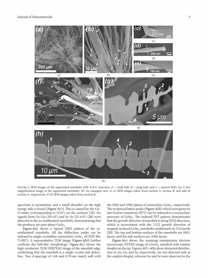
Figure 2 shows the SEM images of the as-prepared nanobelts.As can be seen from the SEM images, most of the nanobeltshave segmented A-B-C structure (A = wide belt, B =zigzag belt, and C = narrow belt). The length of the A-B-Cstructured nanobelts varies from hundreds of micrometersto millimeters (Figures 2(a) and 2(b)). Sections A and Care commonly seen belt-like structure (Figures 2(c)–2(e)).The thickness of most segmented nanobelts ranged from60 to 200 nm (Figure 2(e)). Besides, section C is narrowerthan section A. In Figure 2(d), particle (catalyst) can beclearly observed due to contrast difference, indicating thatVLS mechanism probably dominates the growth of the A-B-C structured nanobelts. Interestingly, section B has zigzagstructure. Figure 2(f) clearly reveals that the zigzag structure(indicated by arrows) serves as a transition region connectingsections A and C. Figures 2(g) and 2(h) show the enlargedviews of section B and the zigzag structure is clearly observed.It is well known that there is a good correlation betweenthe nanobelt diameter and the catalyst size during VLSgrowth [22]. Although the size of section C and particle onthe tip match well, section B has different shape and size.Therefore, VLS mechanism only partly makes contributionto the growth of nanobelt possibly. As can be seen fromFigures 2(g) and 2(h), the growth of flake-like branch onthe backbone might be governed by vapor solid (VS) ratherthan VLS mechanism. Besides, some small branches werealso observed possibly due to different growth stages. As alayer-structured chalcogenides, GeSe
2consists of Se-Ge-Se
layers stacked together via van derWaals interaction [20].Thebranches with different thickness are found (e.g., indicatedby arrows 3 and 4 in Figure 2(h)), implying that eachlayer has different growth speed. The segmented nanobeltshave uniform thickness at section A. Besides, the growthdirection is from section A to C according to the top growthmechanism. Therefore, it is reasonable to conclude that thezigzag structures are not an ultimate state and they wouldgrow into nanobelt with the same structure as section A ifgrowth continues.
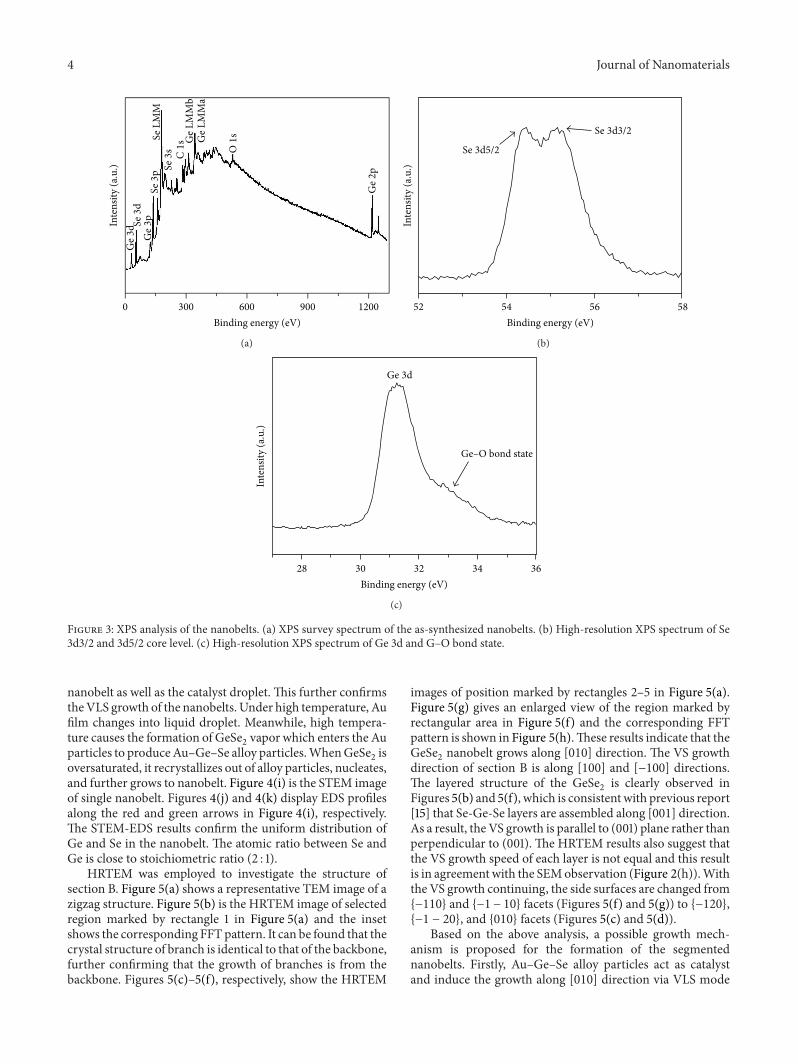
XPS was employed to derive composition informationof the as-synthesized nanobelts. The binding energy of allthe survey and finely scanned spectrums was calibrated bythe standard reference of the C 1s (284.8 eV) signal. TypicalXPS survey spectrum (Figure 3(a)) indicates the presenceof Ge and Se. Figure 3(b) shows that the peaks of Se 3d3/2and Se 3d5/2 core level are at 55.1 and 54.4 eV, respectively.The peak position of Ge 3d core level is at 31.1 eV whichis consistent with the literature [20]. The Ge 3d core level
Journal of Nanomaterials 3
(a)
(f) (g)
(h)
(b)
(c)
(d)
(e)
Figure 2: SEM images of the segmented nanobelts with A-B-C structure (A = wide belt, B = zizag belt, and C = narrow belt). (a) A lowmagnification image of the segmented nanobelts. (b) An enlarged view. (c–e) SEM images taken from section A, section B, and side ofsection A, respectively. (f–h) SEM images taken from section B.
spectrum is asymmetric and a small shoulder on the highenergy side is found (Figure 3(c)). This is caused by the Ge–O states (corresponding to 33 eV) on the surfaces [23]. Nosignals from Ge–Ge (29.1 eV) and Se–Se (55.4 eV) [20] weredetected in the as-synthesized nanobelts, demonstrating thatthe products are pure phase GeSe
2.
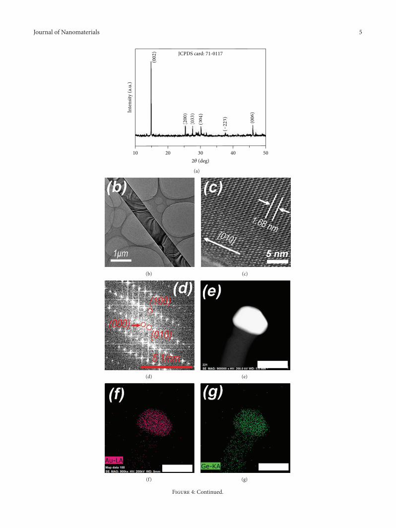
Figure 4(a) shows a typical XRD pattern of the as-synthesized nanobelts. All the diffraction peaks can beindexed to single-crystalline monoclinic GeSe
2(JCPDS file:
71-0117). A representative TEM image (Figure 4(b)) furtherconfirms the belt-like morphology. Figure 4(c) shows thehigh-resolution TEM (HRTEM) image of the nanobelt edge,confirming that the nanobelt is a single crystal and defect-free. Two d-spacings of 1.68 and 0.70 nm match well with
the (010) and (100) planes of monoclinic GeSe2, respectively.
The reciprocal lattice peaks (Figure 4(d)) whichwere given byfast Fourier transform (FFT) can be indexed to a monoclinicstructure of GeSe
2. The indexed FFT pattern demonstrates
that the growth direction of nanobelt is along [010] direction,which is inconsistent with the [112] growth direction ofstepped-surfaced GeSe
2nanobelts synthesized via VLSmode
[20]. The top and bottom surfaces of the nanobelts are {001}facets, and the side surfaces are {100} facets.
Figure 4(e) shows the scanning transmission electronmicroscope (STEM) image of a GeSe
2nanobelt with catalyst
droplet on the tip. Figures 4(f)–4(h) show elemental distribu-tion of Au, Ge, and Se, respectively. Au was detected only atthe catalyst droplet, whereas Ge and Se were observed in the
4 Journal of Nanomaterials
0 300 600 900 1200
Binding energy (eV)
Inte
nsity
(a.u
.)G
e3d Se
3d
Ge3
pSe
3p
Se L
MM
Se3
s C1
s Ge L
MM
bG
e LM
Ma
O1
s
Ge2
p
(a)
Binding energy (eV)
Inte
nsity
(a.u
.)
Se 3d5/2
Se 3d3/2
52 54 56 58
(b)
Binding energy (eV)
Inte
nsity
(a.u
.)
Ge 3d
28 30 32 34 36
Ge–O bond state
(c)
Figure 3: XPS analysis of the nanobelts. (a) XPS survey spectrum of the as-synthesized nanobelts. (b) High-resolution XPS spectrum of Se3d3/2 and 3d5/2 core level. (c) High-resolution XPS spectrum of Ge 3d and G–O bond state.
nanobelt as well as the catalyst droplet. This further confirmstheVLS growth of the nanobelts. Under high temperature, Aufilm changes into liquid droplet. Meanwhile, high tempera-ture causes the formation of GeSe
2vapor which enters the Au
particles to produceAu–Ge–Se alloy particles.WhenGeSe2is
oversaturated, it recrystallizes out of alloy particles, nucleates,and further grows to nanobelt. Figure 4(i) is the STEM imageof single nanobelt. Figures 4(j) and 4(k) display EDS profilesalong the red and green arrows in Figure 4(i), respectively.The STEM-EDS results confirm the uniform distribution ofGe and Se in the nanobelt. The atomic ratio between Se andGe is close to stoichiometric ratio (2 : 1).
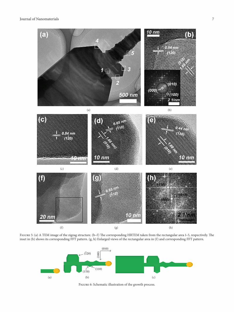
HRTEM was employed to investigate the structure ofsection B. Figure 5(a) shows a representative TEM image of azigzag structure. Figure 5(b) is the HRTEM image of selectedregion marked by rectangle 1 in Figure 5(a) and the insetshows the corresponding FFTpattern. It can be found that thecrystal structure of branch is identical to that of the backbone,further confirming that the growth of branches is from thebackbone. Figures 5(c)–5(f), respectively, show the HRTEM
images of position marked by rectangles 2–5 in Figure 5(a).Figure 5(g) gives an enlarged view of the region marked byrectangular area in Figure 5(f) and the corresponding FFTpattern is shown in Figure 5(h).These results indicate that theGeSe2nanobelt grows along [010] direction. The VS growth
direction of section B is along [100] and [−100] directions.The layered structure of the GeSe
2is clearly observed in
Figures 5(b) and 5(f), which is consistentwith previous report[15] that Se-Ge-Se layers are assembled along [001] direction.As a result, the VS growth is parallel to (001) plane rather thanperpendicular to (001). The HRTEM results also suggest thatthe VS growth speed of each layer is not equal and this resultis in agreementwith the SEMobservation (Figure 2(h)).Withthe VS growth continuing, the side surfaces are changed from{−110} and {−1 − 10} facets (Figures 5(f) and 5(g)) to {−120},{−1 − 20}, and {010} facets (Figures 5(c) and 5(d)).
Based on the above analysis, a possible growth mech-anism is proposed for the formation of the segmentednanobelts. Firstly, Au–Ge–Se alloy particles act as catalystand induce the growth along [010] direction via VLS mode
Journal of Nanomaterials 5
10 20 30 40 50
2𝜃 (deg)(002
)
(200
)(033
)(004
)
(−223
)
(006
)
JCPDS card: 71-0117
(
(200
)(033
)(004
)
(−223
)
(006
)Inte
nsity
(a.u
.)
(a)
(b) (c)
(d) (e)
(f) (g)
Figure 4: Continued.
6 Journal of Nanomaterials
(h) (i)
100
80
60
40
20
0
Cou
nts (
cps)
Position (𝜇m)
SeGe
0.0 0.5 1.0 1.5 2.0 2.5
(j)
100
80
60
40
20
0
Cou
nts (
cps)
Position (𝜇m)
SeGe
0.0 0.5 1.0 1.5 2.0 2.5
(k)
Figure 4: (a) XRD pattern of the nanobelts. (b) A TEM image of a nanobelt. (c, d) A HRTEM taken from the edge of the nanobelt andcorresponding FFT pattern. (e) A STEM image taken from the tip of a nanobelt. (f–h) EDS maps for Au, Gen and Se, respectively. Scale bar:100 nm. (i) A STEM image of the nanobelt. Scale bar: 1 𝜇m. (j, k) EDS profiles taken along the red and green arrows in (i), respectively.
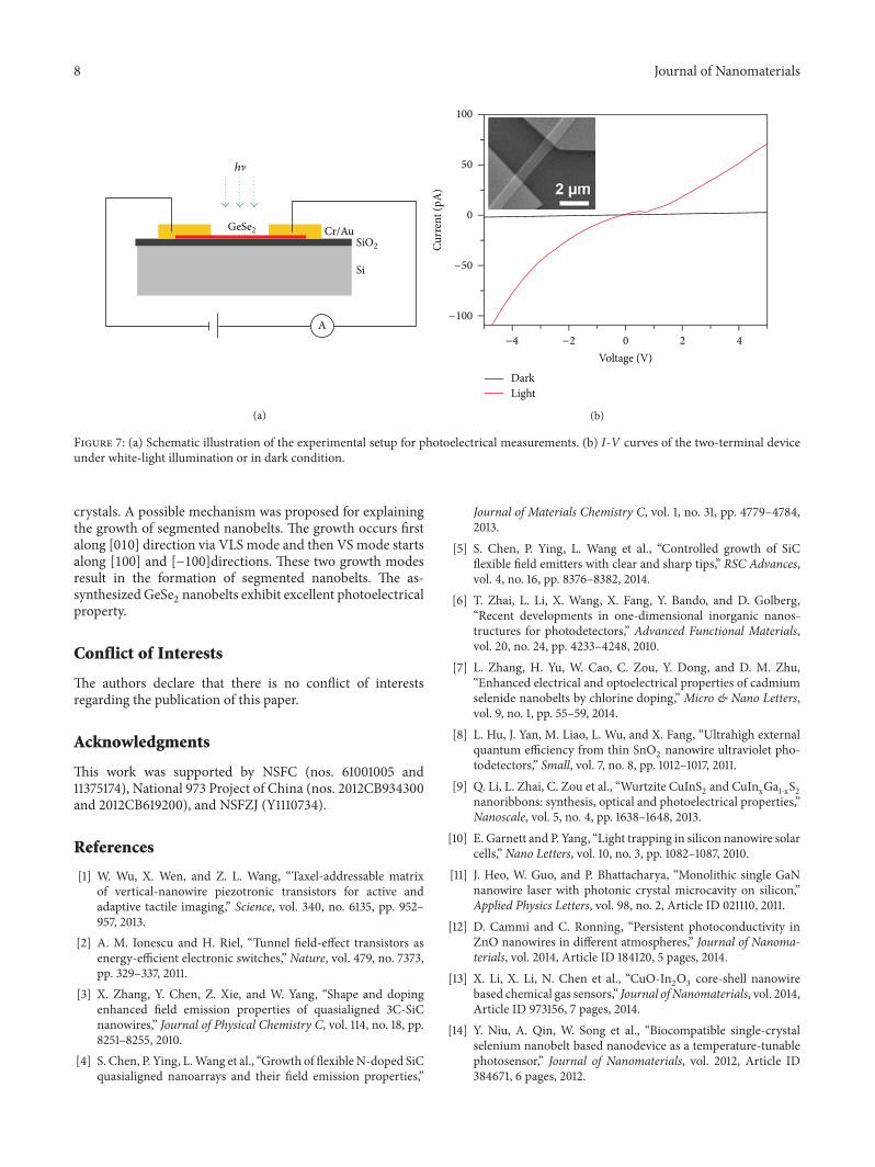
(Figure 6(a)). The two side surfaces of a nanobelt in thisgrowth stage are parallel to (100) plane. Once the narrownanobelt is formed, its side surfaces become nucleation siteswhich direct theVS growth along [100] and [−100] directions(Figure 6(b)). However, because the growth speed of theVLS mode is faster than that of VS mode, zigzag structureforms (Figure 6(b)).With theVLS andVS growth proceedingsimultaneously, the zigzag product evolutes to nanobelt withthe structure of section A and the length of the section Cfurther increase (Figure 6(c)), resulting in the formation ofA-B-C structured products.
Compared with bulk materials, nanostructured semi-conductors have large surface-to-volume ratio and danglingbonds on the material surfaces. Therefore, there are numer-ous oxygenmolecules absorbed on their surface which attractthe electron of photoexcited carriers (O2 + e− → O
2
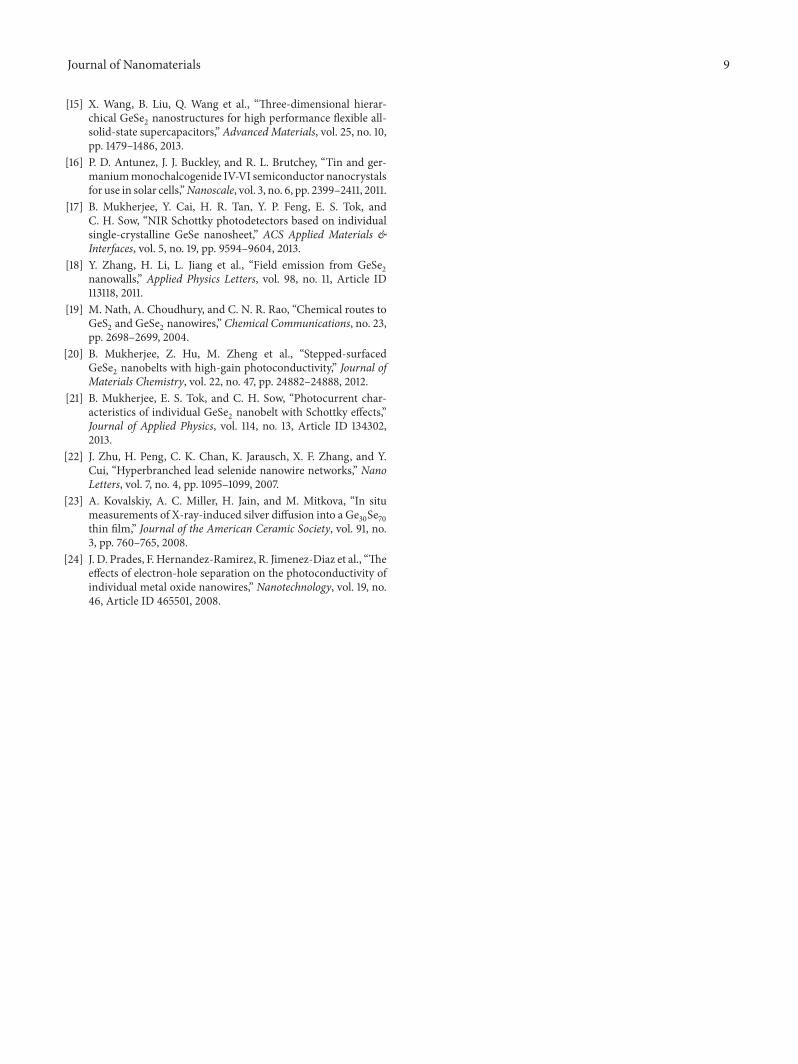
−).This can improve the separation of photoexcited carriers andincrease photocurrent [24]. To evaluate the photoelectricalproperties of the as-synthesized nanobelts, two-terminaldevice was fabricated through using a single GeSe
2nanobelt.
Figure 7(a) shows the schematic illustration of experimentalsetup for photoelectrical measurements. A white light withpower density of ∼0.7mW/mm2 was used as the incidentlight. Figure 7(b) gives the current-voltage (I-V) charac-teristics of the device under incident light illumination orwithout illumination. The asymmetry and nonlinearity of I-V curves indicate the formation of Schottky contact betweenthe nanobelt and the metal electrodes. Compared with thedark current at a bias of 1 V, the photocurrent increases by∼52times. This indicates that the as-synthesized nanobelts havegood photoelectrical properties.
4. Conclusion
In summary, we demonstrated that a simple thermal evapo-ration method could be used to synthesize GeSe
2nanobelts
through using gold particles as catalyst and GeSe2flakes
as starting materials. Most of nanobelts have wide belt,zigzag belt, or narrow belt structures which are mostly single
Journal of Nanomaterials 7
(a) (b)
(c) (d) (e)
(f) (g) (h)
Figure 5: (a) A TEM image of the zigzag structure. (b–f) The corresponding HRTEM taken from the rectangular area 1–5, respectively. Theinset in (b) shows its corresponding FFT pattern. (g, h) Enlarged views of the rectangular area in (f) and corresponding FFT pattern.
(a)
(110)
(100)
(010)
(110)
(120)
(b) (c)
Figure 6: Schematic illustration of the growth process.
8 Journal of Nanomaterials
h�
GeSe2 Cr/AuSiO2
Si
A
(a)
100
50
0
−50
−100
Curr
ent (
pA)
−4 −2 0 2 4
Voltage (V)
DarkLight
(b)
Figure 7: (a) Schematic illustration of the experimental setup for photoelectrical measurements. (b) I-V curves of the two-terminal deviceunder white-light illumination or in dark condition.
crystals. A possible mechanism was proposed for explainingthe growth of segmented nanobelts. The growth occurs firstalong [010] direction via VLS mode and then VS mode startsalong [100] and [−100]directions. These two growth modesresult in the formation of segmented nanobelts. The as-synthesized GeSe
2nanobelts exhibit excellent photoelectrical
property.
Conflict of Interests
The authors declare that there is no conflict of interestsregarding the publication of this paper.
Acknowledgments
This work was supported by NSFC (nos. 61001005 and11375174), National 973 Project of China (nos. 2012CB934300and 2012CB619200), and NSFZJ (Y1110734).
References
[1] W. Wu, X. Wen, and Z. L. Wang, “Taxel-addressable matrixof vertical-nanowire piezotronic transistors for active andadaptive tactile imaging,” Science, vol. 340, no. 6135, pp. 952–957, 2013.
[2] A. M. Ionescu and H. Riel, “Tunnel field-effect transistors asenergy-efficient electronic switches,” Nature, vol. 479, no. 7373,pp. 329–337, 2011.
[3] X. Zhang, Y. Chen, Z. Xie, and W. Yang, “Shape and dopingenhanced field emission properties of quasialigned 3C-SiCnanowires,” Journal of Physical Chemistry C, vol. 114, no. 18, pp.8251–8255, 2010.
[4] S. Chen, P. Ying, L.Wang et al., “Growth of flexible N-doped SiCquasialigned nanoarrays and their field emission properties,”
Journal of Materials Chemistry C, vol. 1, no. 31, pp. 4779–4784,2013.
[5] S. Chen, P. Ying, L. Wang et al., “Controlled growth of SiCflexible field emitters with clear and sharp tips,” RSC Advances,vol. 4, no. 16, pp. 8376–8382, 2014.
[6] T. Zhai, L. Li, X. Wang, X. Fang, Y. Bando, and D. Golberg,“Recent developments in one-dimensional inorganic nanos-tructures for photodetectors,” Advanced Functional Materials,vol. 20, no. 24, pp. 4233–4248, 2010.
[7] L. Zhang, H. Yu, W. Cao, C. Zou, Y. Dong, and D. M. Zhu,“Enhanced electrical and optoelectrical properties of cadmiumselenide nanobelts by chlorine doping,” Micro & Nano Letters,vol. 9, no. 1, pp. 55–59, 2014.
[8] L. Hu, J. Yan, M. Liao, L. Wu, and X. Fang, “Ultrahigh externalquantum efficiency from thin SnO
2nanowire ultraviolet pho-
todetectors,” Small, vol. 7, no. 8, pp. 1012–1017, 2011.[9] Q. Li, L. Zhai, C. Zou et al., “Wurtzite CuInS
2and CuInxGa1-xS2
nanoribbons: synthesis, optical and photoelectrical properties,”Nanoscale, vol. 5, no. 4, pp. 1638–1648, 2013.
[10] E. Garnett and P. Yang, “Light trapping in silicon nanowire solarcells,” Nano Letters, vol. 10, no. 3, pp. 1082–1087, 2010.
[11] J. Heo, W. Guo, and P. Bhattacharya, “Monolithic single GaNnanowire laser with photonic crystal microcavity on silicon,”Applied Physics Letters, vol. 98, no. 2, Article ID 021110, 2011.
[12] D. Cammi and C. Ronning, “Persistent photoconductivity inZnO nanowires in different atmospheres,” Journal of Nanoma-terials, vol. 2014, Article ID 184120, 5 pages, 2014.
[13] X. Li, X. Li, N. Chen et al., “CuO-In2O3core-shell nanowire
based chemical gas sensors,” Journal of Nanomaterials, vol. 2014,Article ID 973156, 7 pages, 2014.
[14] Y. Niu, A. Qin, W. Song et al., “Biocompatible single-crystalselenium nanobelt based nanodevice as a temperature-tunablephotosensor,” Journal of Nanomaterials, vol. 2012, Article ID384671, 6 pages, 2012.
Journal of Nanomaterials 9
[15] X. Wang, B. Liu, Q. Wang et al., “Three-dimensional hierar-chical GeSe
2nanostructures for high performance flexible all-
solid-state supercapacitors,” Advanced Materials, vol. 25, no. 10,pp. 1479–1486, 2013.
[16] P. D. Antunez, J. J. Buckley, and R. L. Brutchey, “Tin and ger-maniummonochalcogenide IV-VI semiconductor nanocrystalsfor use in solar cells,”Nanoscale, vol. 3, no. 6, pp. 2399–2411, 2011.
[17] B. Mukherjee, Y. Cai, H. R. Tan, Y. P. Feng, E. S. Tok, andC. H. Sow, “NIR Schottky photodetectors based on individualsingle-crystalline GeSe nanosheet,” ACS Applied Materials &Interfaces, vol. 5, no. 19, pp. 9594–9604, 2013.
[18] Y. Zhang, H. Li, L. Jiang et al., “Field emission from GeSe2
nanowalls,” Applied Physics Letters, vol. 98, no. 11, Article ID113118, 2011.
[19] M. Nath, A. Choudhury, and C. N. R. Rao, “Chemical routes toGeS2and GeSe
2nanowires,” Chemical Communications, no. 23,
pp. 2698–2699, 2004.[20] B. Mukherjee, Z. Hu, M. Zheng et al., “Stepped-surfaced
GeSe2nanobelts with high-gain photoconductivity,” Journal of
Materials Chemistry, vol. 22, no. 47, pp. 24882–24888, 2012.[21] B. Mukherjee, E. S. Tok, and C. H. Sow, “Photocurrent char-
acteristics of individual GeSe2nanobelt with Schottky effects,”
Journal of Applied Physics, vol. 114, no. 13, Article ID 134302,2013.
[22] J. Zhu, H. Peng, C. K. Chan, K. Jarausch, X. F. Zhang, and Y.Cui, “Hyperbranched lead selenide nanowire networks,” NanoLetters, vol. 7, no. 4, pp. 1095–1099, 2007.
[23] A. Kovalskiy, A. C. Miller, H. Jain, and M. Mitkova, “In situmeasurements of X-ray-induced silver diffusion into a Ge
30Se70
thin film,” Journal of the American Ceramic Society, vol. 91, no.3, pp. 760–765, 2008.
[24] J. D. Prades, F. Hernandez-Ramirez, R. Jimenez-Diaz et al., “Theeffects of electron-hole separation on the photoconductivity ofindividual metal oxide nanowires,” Nanotechnology, vol. 19, no.46, Article ID 465501, 2008.

Submit your manuscripts athttp://www.hindawi.com
ScientificaHindawi Publishing Corporationhttp://www.hindawi.com Volume 2014
CorrosionInternational Journal of
Hindawi Publishing Corporationhttp://www.hindawi.com Volume 2014
Polymer ScienceInternational Journal of
Hindawi Publishing Corporationhttp://www.hindawi.com Volume 2014
Hindawi Publishing Corporationhttp://www.hindawi.com Volume 2014
CeramicsJournal of
Hindawi Publishing Corporationhttp://www.hindawi.com Volume 2014
CompositesJournal of
NanoparticlesJournal of
Hindawi Publishing Corporationhttp://www.hindawi.com Volume 2014
Hindawi Publishing Corporationhttp://www.hindawi.com Volume 2014
International Journal of
Biomaterials
Hindawi Publishing Corporationhttp://www.hindawi.com Volume 2014
NanoscienceJournal of
TextilesHindawi Publishing Corporation http://www.hindawi.com Volume 2014
Journal of
NanotechnologyHindawi Publishing Corporationhttp://www.hindawi.com Volume 2014
Journal of
CrystallographyJournal of
Hindawi Publishing Corporationhttp://www.hindawi.com Volume 2014
The Scientific World JournalHindawi Publishing Corporation http://www.hindawi.com Volume 2014
Hindawi Publishing Corporationhttp://www.hindawi.com Volume 2014
CoatingsJournal of
Advances in
Materials Science and EngineeringHindawi Publishing Corporationhttp://www.hindawi.com Volume 2014
Smart Materials Research
Hindawi Publishing Corporationhttp://www.hindawi.com Volume 2014
Hindawi Publishing Corporationhttp://www.hindawi.com Volume 2014
MetallurgyJournal of
Hindawi Publishing Corporationhttp://www.hindawi.com Volume 2014
BioMed Research International
MaterialsJournal of
Hindawi Publishing Corporationhttp://www.hindawi.com Volume 2014
Nano
materials
Hindawi Publishing Corporationhttp://www.hindawi.com Volume 2014
Journal ofNanomaterials


![Synthesis and Characterization of [n]Cumulenes](https://img.pdfslide.org/doc/110x75/58a181de1a28abb24d8c126c/synthesis-and-characterization-of-ncumulenes-.jpg)