Embed Size (px)
Citation preview
INSTITUT FÜR ANGEWANDTE PHYSIKPhysikalisches Praktikum für Studierende der Ingenieurswissenschaften
Universität Hamburg, Jungiusstraÿe 11
RLC Circuit
Contents
1 RCL Series Circuit 3
2 Set-Up of the Experiment 3
3 Additional Insights 3
4 Basics 44.1 Glossary . . . . . . . . . . . . . . . . . . . . . . . . . . . . . . . . . . . . . 44.2 Capacity C . . . . . . . . . . . . . . . . . . . . . . . . . . . . . . . . . . . 64.3 Inductance L: Inductor in a DC circuit . . . . . . . . . . . . . . . . . . . . 84.4 Impedance Z, apparent impedance |Z . . . . . . . . . . . . . . . . . . . . . 8
5 An Ideal Oscillating Circuit 9
6 Realistic RLC Oscillating Circuit 106.1 Impedanz,apparent impedance . . . . . . . . . . . . . . . . . . . . . . . . . 106.2 Current and Voltage . . . . . . . . . . . . . . . . . . . . . . . . . . . . . . 10
7 Exercise: Setup of a RLC Oscillating Circuit 147.1 Calculate theoretical values . . . . . . . . . . . . . . . . . . . . . . . . . . 147.2 Loss Resistance of an inductor . . . . . . . . . . . . . . . . . . . . . . . . . 147.3 Measurement Setup . . . . . . . . . . . . . . . . . . . . . . . . . . . . . . . 147.4 Determining Resonance and Cuto� Frequencies using Lissajous -Figure . . 157.5 Transfer Function and Impedance: Z,Rv . . . . . . . . . . . . . . . . . . . 157.6 Bandwidth B, Q Factor, Cuto� Frequencies . . . . . . . . . . . . . . . . . 167.7 Signal shape . . . . . . . . . . . . . . . . . . . . . . . . . . . . . . . . . . . 16
1
8 Questions and Preparation 16
9 Literatur 17
10 10. Appendix: Relationship between current and voltage 17
11 Additional Exercises (optional) 1911.1 RL High-Pass Filter . . . . . . . . . . . . . . . . . . . . . . . . . . . . . . . 1911.2 RC low-pass �lter . . . . . . . . . . . . . . . . . . . . . . . . . . . . . . . . 20
2
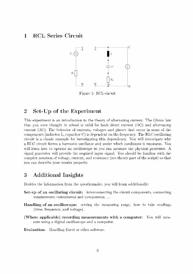
1 RCL Series Circuit
B
Ri
Ue
A
B
L
C
Rd
i
A
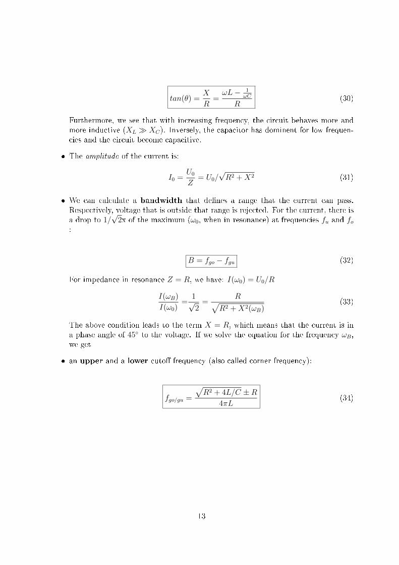
D
C
V
Figure 1: RCL-circuit
2 Set-Up of the Experiment
This experiment is an introduction to the theory of alternating current. The Ohmic lawthat you were thought in school is valid for both direct current (DC) and alternatingcurrent (AC). The behavior of currents, voltages and phases that occur in some of thecomponents (inductor L, capacitor C) is dependent on the frequency. The RLC oscillatingcircuit is a classic example for investigating this dependency. You will investigate whya RLC circuit forms a harmonic oscillator and under which conditions it resonates. Youwill learn how to operate an oscilloscope so you can measure the physical processes. Asignal generator will provide the required input signal. You should be familiar with thecomplex notation of voltage, current, and resistance (see theory part of the script) so thatyou can describe your results properly.
3 Additional Insights
Besides the information from the questionnaire, you will learn additionally:
Set-up of an oscillating circuit: interconnecting the circuit components, connectingmeasurement instruments and components, ...
Handling of an oscilloscope: setting the measuring range, how to take readings(time, frequency, and voltage).
(Where applicable) recording measurements with a computer: You will mea-sure using a digital oscilloscope and a computer.
Evaluation: Handling Excel or other software.
3
4 Basics
4.1 Glossary
Here, we brie�y introduce some terms. For a more detailed explanation, we refer to therespective literature.
The electric �eld and the voltage U If a small probing charge q=e− is in the closevicinity of a much larger charge, a force (depending on the sign, by convention) actson the probing charge (see Law of Coulomb, which should be familiar to you). Thisleads to the (vectorial) de�nition of the electric �eld E
E(r) =F(r)
q[E] =
N
C(1)
The charge is displaced when a force acts on it. Thus, depending on the directionof the applied force and the sign of the charge, electrical work W would be eitherconsumed or generated by displacing dr the probing charge.
W1,2 =
∫ 2
1
Fdr = q
∫ 2
1
Edr = qEd = q
∫ 2
1
dϕ = qU (2)
E(r) =dϕ
drer [E] =
V
m(3)
In a battery, a conductor connects two electric poles with di�erent charge carrierconcentration and the potential ϕ. If this is the case, the charge carriers will evenmove through a �ow of current. Then, Ohmic law applies: U = R · I.Furthermore, from eqn. (2) follows :
qU
q=qEd
q→ U = Ed (4)
The �eld strength can be determined much easier using the distance and the voltage.
Kirchho�'s node law The principle of conservation of electric charge implies that atany node (or junction) in an electrical circuit, the sum of currents in a network ofconductors meeting at a point is zero.
∑i
Ii = 0 (5)
Kirchho�'s loop law The sum of the electrical potential di�erences (voltage) aroundany closed network is zero. Therefore, the following law is derived:∑
i
Ui = 0 (6)
4
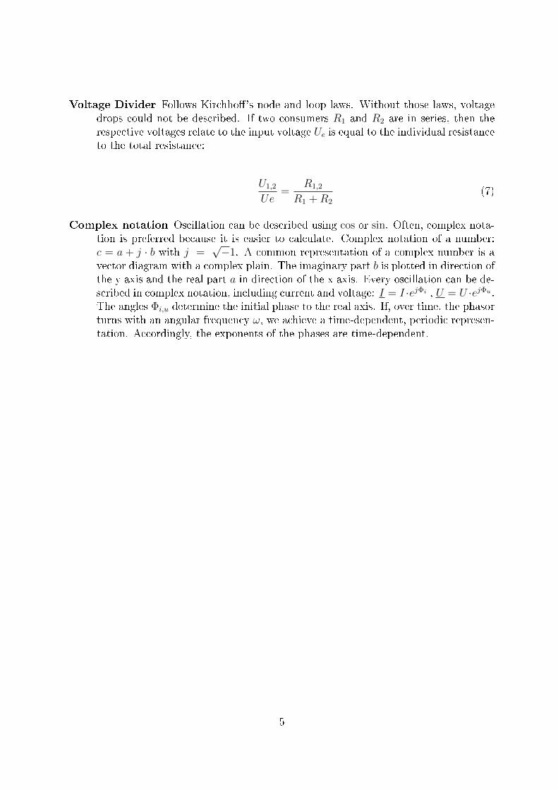
Voltage Divider Follows Kirchho�'s node and loop laws. Without those laws, voltagedrops could not be described. If two consumers R1 and R2 are in series, then therespective voltages relate to the input voltage Ue is equal to the individual resistanceto the total resistance:
U1,2
Ue=
R1,2
R1 +R2
(7)
Complex notation Oscillation can be described using cos or sin. Often, complex nota-tion is preferred because it is easier to calculate. Complex notation of a number:c = a + j · b with j =
√−1. A common representation of a complex number is a
vector diagram with a complex plain. The imaginary part b is plotted in direction ofthe y axis and the real part a in direction of the x axis. Every oscillation can be de-scribed in complex notation, including current and voltage: I = I ·ejΦi , U = U ·ejΦu .The angles Φi,u determine the initial phase to the real axis. If, over time, the phasorturns with an angular frequency ω, we achieve a time-dependent, periodic represen-tation. Accordingly, the exponents of the phases are time-dependent.
5
4.2 Capacity C
Capacity A capacity is a property of a capacitor. If a voltage U is applied, a capacitorcollects a certain amount of charge carriers Q and later releases them. The energythat is needed for separation of charge is partially (Ohmic loss) stored in the electric�eld that builds up during charging.
C =Q
U[C] =
1AS = C
V= 1F (Farad) (8)
W =1
2CU2 [W ] = 1Ws = 1Joule (9)
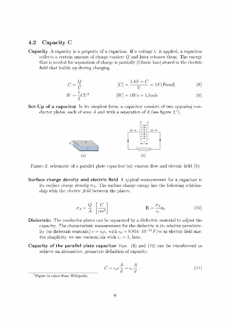
Set-Up of a capacitor In its simplest form, a capacitor consists of two opposing con-ductor plates, each of area A and with a separation of d (see �gure 2.1).
(a) (b)
Figure 2: schematic of a parallel plate capacitor (a); current �ow and electric �eld (b)
Surface charge density and electric �eld A typical measurement for a capacitor isits surface charge density σA. The surface charge energy has the following relation-ship with the electric �eld between the plates:
σA =Q
A
[C
cm2
]E =
σAεr
er (10)
Dielectric: The conductor plates can be separated by a dielectric material to adjust thecapacity. The characteristic measurement for the dielectric is its relative permittiv-ity (or dielectric constant) ε = ε0εr with ε0 = 8.854 · 10−12 F/m as electric �eld size.For simplicity, we use vacuum/air with εr = 1, here.
Capacity of the parallel plate capacitor Eqn. (8) and (10) can be transformed toachieve an alternative, geometric de�nition of capacity:
C = εoεA
d= εr
A
d(11)
1Figure is taken from Wikipedia
6
Halving the distance between capacitor plates The e�ect of halving the distanced for a charged capacitor
C = εrA
d0/2= 2C0 (12)
is dependent on it connection to the voltage source:
1. If the capacitor was disconnected from the voltage source, charge Q ispreserved; i) Surface charge density is constant : σA = const.→ ii) Field strength is constant: E = σA/εr = konst → iii) Voltage isreduced by half: U = Ed0/2 = U0/2 The energy is reduced to half too,W = 1/2(2C0)(U0/2)2 = W0/2. That means, the energy is released
W01 =
∫ d0/2
d0
Fds = Q
∫ d0/2
d0
Eds = −1
2W0 (13)
Invertedly, energy has to be spent for separation of charges. That energy issaved in the electric �eld.
2. If the capacitor was not disconnected from the voltage source, voltagestays constant U = const. but charge Q 6= 0 is not preserved. Charges can�ow to and from the voltage source. i) Surface charge density doubles becauseU=const. and Equ.(12): → σA = const. → ii) Field strength is doubled:E = 2σA0/εr = 2E0 Energy content is doubled W = 1/2(2C0)U2 = 2W0.
Charging properties of a RC element A capacitor's time propertiy is described bya di�erential equation. Kirchho�'s loop law, applied to the RC element.
UR + Uc = RI +Q
C= Ue (14)
RdQ
dt+Q
C= Ue (15)
I =dQ
dt=dCU
dt=CdU
dt(16)
Capacitive Reactance
XC =1
ωC(17)
7
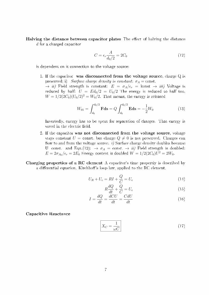
Figure 3: RC low-pass: left, simulation of a RC low-pass �lter; right, measured values Ucand I. The same components as in the experiment were used (R=47 Ohm and C=0.1 µF )
4.3 Inductance L: Inductor in a DC circuit
According to Lenz's law, a changing electric current through a inductor induces a propor-tional voltage, which opposes the change in the current.
Uind = −LdIdt
[L] =1V s
A= 1F (Henry) (18)
WL =1
2LI2 [W ] = 1Ws = 1Joule (19)
Applying voltage to a inductor creates a current that increases exponentially to amaximum with a time constant τL = L/R and iL = U/R · (1 − e−t/τ ). The inductivereactance XL does not work as an active power but preserves energy as magnetic �eld.The active resistance RvL causes ohmic heating. The inductive Q factor is measured fordetermining the thermal loss QL = ωL/R
Inductive Reactance
XL = ωL (20)
4.4 Impedance Z, apparent impedance |Z|The impedance Z in an AC circuit is the complex ratio of the active resistance R (caus-ing Ohmic heating) to the frequency-dependent inductive reactance X.
Z = R + jX. The absolute value Z = |Z| =√R2 + (ωL− 1
ωC)2 is called apparent
impedance.
8
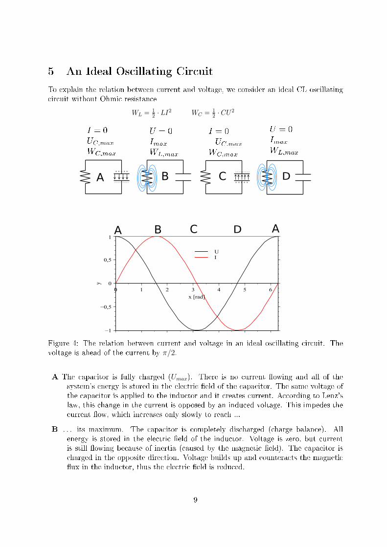
5 An Ideal Oscillating Circuit
To explain the relation between current and voltage, we consider an ideal CL oscillatingcircuit without Ohmic resistance
+ + + + +
- - - - - - - - - + + + + +
- - - - - - - - -
A B C D
A B C D A
Figure 4: The relation between current and voltage in an ideal oscillating circuit. Thevoltage is ahead of the current by π/2.
A The capacitor is fully charged (Umax). There is no current �owing and all of thesystem's energy is stored in the electric �eld of the capacitor. The same voltage ofthe capacitor is applied to the inductor and it creates current. According to Lenz'slaw, this change in the current is opposed by an induced voltage. This impedes thecurrent �ow, which increases only slowly to reach ...
B . . . its maximum. The capacitor is completely discharged (charge balance). Allenergy is stored in the electric �eld of the inductor. Voltage is zero, but currentis still �owing because of inertia (caused by the magnetic �eld). The capacitor ischarged in the opposite direction. Voltage builds up and counteracts the magnetic�ux in the inductor, thus the electric �eld is reduced.
9
C The current reaches a minimum (I=0) when voltage reaches its maximum Umax. Thecapacitor is fully charged in the opposite direction.
The capacitor discharges like described in A but with the inverse sign.
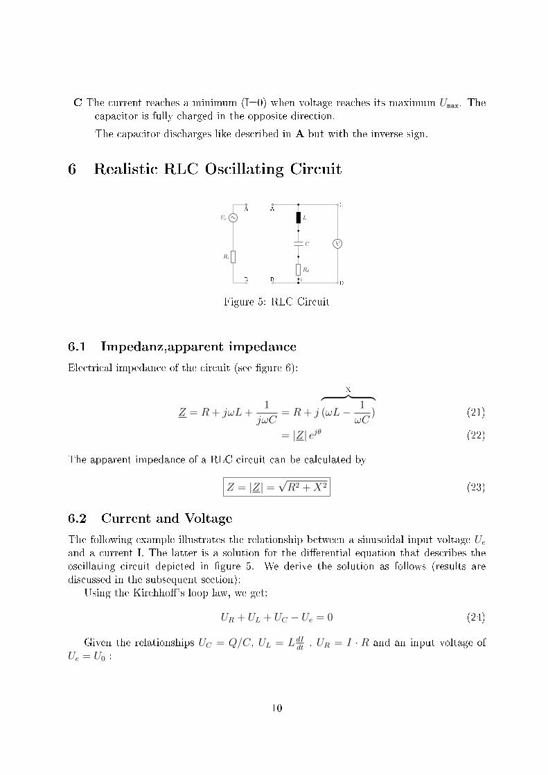
6 Realistic RLC Oscillating Circuit
B
Ri
Ue
A
B
L
C
Rd
i
A
D
C
V
Figure 5: RLC Circuit
6.1 Impedanz,apparent impedance
Electrical impedance of the circuit (see �gure 6):
Z = R + jωL+1
jωC= R + j
X︷ ︸︸ ︷(ωL− 1
ωC) (21)
= |Z| ejθ (22)
The apparent impedance of a RLC circuit can be calculated by
Z = |Z| =√R2 +X2 (23)
6.2 Current and Voltage
The following example illustrates the relationship between a sinusoidal input voltage Ueand a current I. The latter is a solution for the di�erential equation that describes theoscillating circuit depicted in �gure 5. We derive the solution as follows (results arediscussed in the subsequent section):
Using the Kirchho�'s loop law, we get:
UR + UL + UC − Ue = 0 (24)
Given the relationships UC = Q/C, UL = LdIdt
, UR = I · R and an input voltage ofUe = U0 :
10
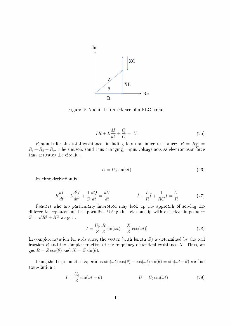
Figure 6: About the impedance of a RLC circuit
IR + LdI
dt+Q
C= U. (25)
R stands for the total resistance, including loss and inner resistance: R = R∑ =Ri +Rd +Rv. The sinusoid (and thus changing) input voltage acts as electromotor forcethat activates the circuit :
U = U0 sin(ωt) (26)
Its time derivation is :
RdI
dt+ L
d2I
dt2+
1
C
dQ
dt=dU
dtI +
L
RI +
1
RCI =
U
R(27)
Readers who are particularly interested may look up the approach of solving thedi�erential equation in the appendix. Using the relationship with electrical impedanceZ =
√R2 +X2 we get :
I =U0
Z[R
Zsin(ωt)− X
Zcos(ωt)] (28)
In complex notation for resistance, the vector (with length Z) is determined by the realfraction R and the complex fraction of the frequency-dependent resistance X. Thus, weget R = Z cos(θ) and X = Z sin(θ).
Using the trigonometric equations sin(ωt) cos(θ)− cos(ωt) sin(θ) = sin(ωt− θ) we �ndthe solution :
I =U0
Zsin(ωt− θ) U = U0 sin(ωt) (29)
11
6.2.1 Discussion
� From the solution, we can see that current and voltage are out of phase. The currentstays behind by a di�erence of θ. In other words, the voltage is ahead of the currentby θ/ω.
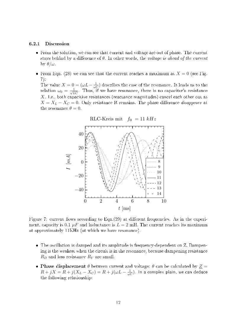
� From Eqn. (28) we can see that the current reaches a maximum at X = 0 (see Fig.7):The value X = 0 = (ωL− 1
ωC) describes the case of the resonance. It leads us to the
relation ω0 = 1√LC
. Thus, if we have resonance, there is no capacitor's resistance
X. I.e., both capacitive resistances (reactance magnitudes) cancel each other out asX = XL −XC = 0. Only resistance R remains. The phase di�erence disappears atthe resonance θ = 0.
Figure 7: current �ows according to Eqn.(29) at di�erent frequencies. As in the experi-ment, capacity is 0.1 µF and inductance is L = 2 mH. The current reaches its maximumat approximately 11KHz (at which we have resonance).
� The oscillation is damped and its amplitude is frequency-dependent on Z. Dampen-ing is the weakest when the circuit is in the resonance, because dampening resistanceRD and loss resistance RV are small.
� Phase displacement θ between current and voltage: θ can be calculated by Z =R + jX = R + j(XL −XC) = R + j(ωL− 1
ωC). In a complex plain, we can deduce
the following relationship:
12
tan(θ) =X
R=ωL− 1
ωC
R(30)
Furthermore, we see that with increasing frequency, the circuit behaves more andmore inductive (XL � XC). Inversely, the capacitor has dominent for low frequen-cies and the circuit become capacitive.
� The amplitude of the current is:
I0 =U0
Z= U0/
√R2 +X2 (31)
� We can calculate a bandwidth that de�nes a range that the current can pass.Respectively, voltage that is outside that range is rejected. For the current, there isa drop to 1/
√2x of the maximum (ω0, when in resonance) at frequencies fu and fo
:
B = fgo − fgu (32)
For impedance in resonance Z = R, we have: I(ω0) = U0/R
I(ωB)
I(ω0)=
1√2
=R√
R2 +X2(ωB)(33)
The above condition leads to the term X = R, which means that the current is ina phase angle of 45◦ to the voltage. If we solve the equation for the frequency ωB,we get
� an upper and a lower cuto� frequency (also called corner frequency):
fgo/gu =
√R2 + 4L/C ±R
4πL(34)
13
7 Exercise: Setup of a RLC Oscillating Circuit
Set up the circuit as depicted in �g. 1, using the following components:
component valueResistance Rd 47 OhmCapacitor 0,1 µ Finductor 2 mH
7.1 Calculate theoretical values
For the above components, calculate :a) Resonance frequency f0 using the condition for resonance: XL = XC
b) Cuto� frequencies, according to Eqn.(34) and Gl.(??)c) Bandwidth of the system according to Eqn.(32)d) The circuit's Q factor as Q = f0
B
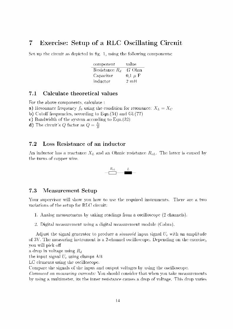
7.2 Loss Resistance of an inductor
An inductor has a reactance XL and an Ohmic resistance RvL. The latter is caused bythe turns of copper wire.
RvL L
7.3 Measurement Setup
Your supervisor will show you how to use the required instruments. There are a twovariations of the setup for RLC circuit:
1. Analog measurement by taking readings from a oscilloscope (2 channels).
2. Digital measurement using a digital measurement module (Cobra).
Adjust the signal generator to produce a sinusoid input signal Ue with an amplitudeof 3V. The measuring instrument is a 2-channel oscilloscope. Depending on the exercise,you will pick o�a drop in voltage using Rd
the input signal Ue using clamps ABLC elements using the oscilloscope.Compare the signals of the input and output voltages by using the oscilloscope.Comment on measuring currents: You should consider that when you take measurementsby using a multimeter, its the inner resistance causes a drop of voltage. This drop varies
14
with the precision of the measurement. One would have to leave the precision unchangedduring the whole experiment and also measure the drop of voltage at the multimeter.Hence, it is recommended to determine the current indirectly via the drop of voltage atthe dampening resistance RD.
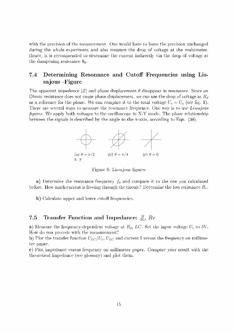
7.4 Determining Resonance and Cuto� Frequencies using Lis-
sajous -Figure
The apparent impedence |Z| and phase displacement θ disappear in resonance. Since anOhmic resistance does not cause phase displacement, we can use the drop of voltage at Rd
as a reference for the phase. We can compare it to the total voltage Ue = Ua (see �g. 1).There are several ways to measure the resonance frequency. One way is to use Lissajous�gures. We apply both voltages to the oscilloscope in X-Y mode. The phase relationshipbetween the signals is described by the angle to the x-axis, according to Eqn. (30).
(a) θ = π/2x=y
(b) θ = π/4 (c) θ = 0
Figure 8: Lissajous �gures
a) Determine the resonance frequency f0 and compare it to the one you calculatedbefore. How much current is �owing through the circuit? Determine the loss resistance Rv.
b) Calculate upper and lower cuto� frequencies.
7.5 Transfer Function and Impedance: Z, Rv
a) Measure the frequency-dependent voltage at Rd, LC. Set the input voltage Ue to 3V.How do you precede with the measurement?b) Plot the transfer function ULC/Ue, ULC and current I versus the frequency on millime-ter paper.c) Plot impedance versus frequency on millimeter paper. Compare your result with thetheoretical impedance (see glossary) and plot them.
15
7.6 Bandwidth B, Q Factor, Cuto� Frequencies
a) a) Determine the upper and lower cuto� frequencies fgo,fgu using the graph of yourmeasurements of U and I. Use the readings to determine the bandwidth. Do the resultsmatch the ones calculated using Eqn..(34), Eqn.(??) and Eqn.(32)? Calculate the Q fac-tor of the system (Q = f0
B)!
b) Why is a series oscillating circuit also called frequency trap?
7.7 Signal shape
In this exercise, we investigate the impulse response to a square-wave signal at di�erentfrequencies.
a) Set the input to a square-wave signal and investigate how the CL system reacts.Plot the impulse response on millimeter paper.b)Change the dampening resistance to 470 Ohm and the inductor to 20mH. What wouldhappen
8 Questions and Preparation
� Determine the resonance frequency f0 for the setup in exercise B, using conditionfor resonance: XL = XC
� Explain the Kircho�'s Law ?
� Describe how voltage and current progress over a capacitor, an ohmic resistor anda inductor when the power supply is turned on and o�!
� What are the physical concepts of Ohmic resistance and apparent impedance Z?Describe impedance, using a series/parallel RLC circuit as an example.
� What is a vector diagram?
� What is phase displacement θ? How is it connected to impedance?
� Which conditions cause resonance?
� What does bandwidth mean?
� What is the Q factor?
16
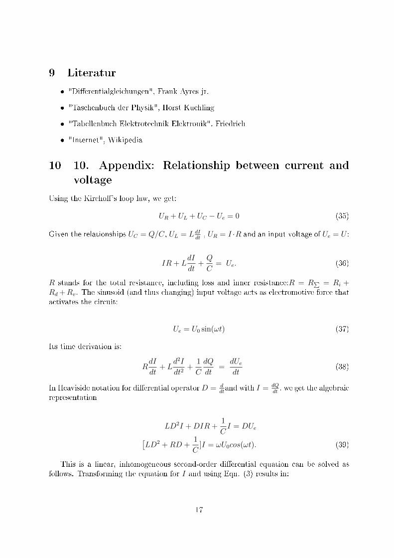
9 Literatur
� "Di�erentialgleichungen", Frank Ayres jr.
� "Taschenbuch der Physik", Horst Kuchling
� "Tabellenbuch Elektrotechnik Elektronik", Friedrich
� "Internet", Wikipedia
10 10. Appendix: Relationship between current and
voltage
Using the Kircho�'s loop law, we get:
UR + UL + UC − Ue = 0 (35)
Given the relationships UC = Q/C, UL = LdIdt, UR = I ·R and an input voltage of Ue = U :
IR + LdI
dt+Q
C= Ue. (36)
R stands for the total resistance, including loss and inner resistance:R = R∑ = Ri +Rd +Rv. The sinusoid (and thus changing) input voltage acts as electromotive force thatactivates the circuit:
Ue = U0 sin(ωt) (37)
Its time derivation is:
RdI
dt+ L
d2I
dt2+
1
C
dQ
dt=
dUedt
(38)
In Heaviside notation for di�erential operatorD = ddtand with I = dQ
dt, we get the algebraic
representation
LD2I +DIR +1
CI = DUe[
LD2 +RD +1
C]I = ωU0cos(ωt). (39)
This is a linear, inhomogeneous second-order di�erential equation can be solved asfollows. Transforming the equation for I and using Eqn. (3) results in:
17
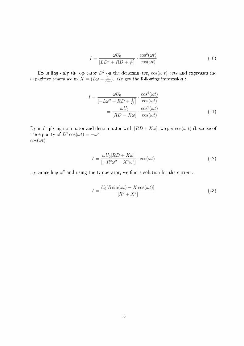
I =ωU0
[LD2 +RD + 1C
] · cos2(ωt)
cos(ωt)(40)
Excluding only the operator D2 on the denominator, cos(ω t) acts and expresses thecapacitive reactance as X = (Lω − 1
Cω). We get the following impression :
I =ωU0
[−Lω2 +RD + 1C
] · cos2(ωt)
cos(ωt)
=ωU0
[RD −Xω]· cos2(ωt)
cos(ωt)(41)
By multiplying nominator and denominator with [RD+Xω], we get cos(ω t) (because ofthe equality of D2 cos(ωt) = −ω2
cos(ωt):
I =ωU0[RD +Xω]
[−R2ω2 −X2ω2]· cos(ωt) (42)
By cancelling ω2 and using the D operator, we �nd a solution for the current:
I =U0[R sin(ωt)−X cos(ωt)]
[R2 +X2](43)
18
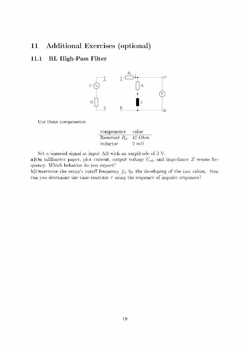
11 Additional Exercises (optional)
11.1 RL High-Pass Filter
B
Ri
V
A
B
Rd i
Rv
L
A
D
C
V
Use these components:
components valueResistant Rd 47 Ohminductor 2 mH
Set a sinusoid signal at input AB with an amplitude of 3 V.a)On millimeter paper, plot current, output voltage Ucd, and impedance Z versus fre-quency. Which behavior do you expect?b)Determine the setup's cuto� frequency fG by the developing of the two values. Howcan you determine the time constant τ using the sequence of impulse responses?
19
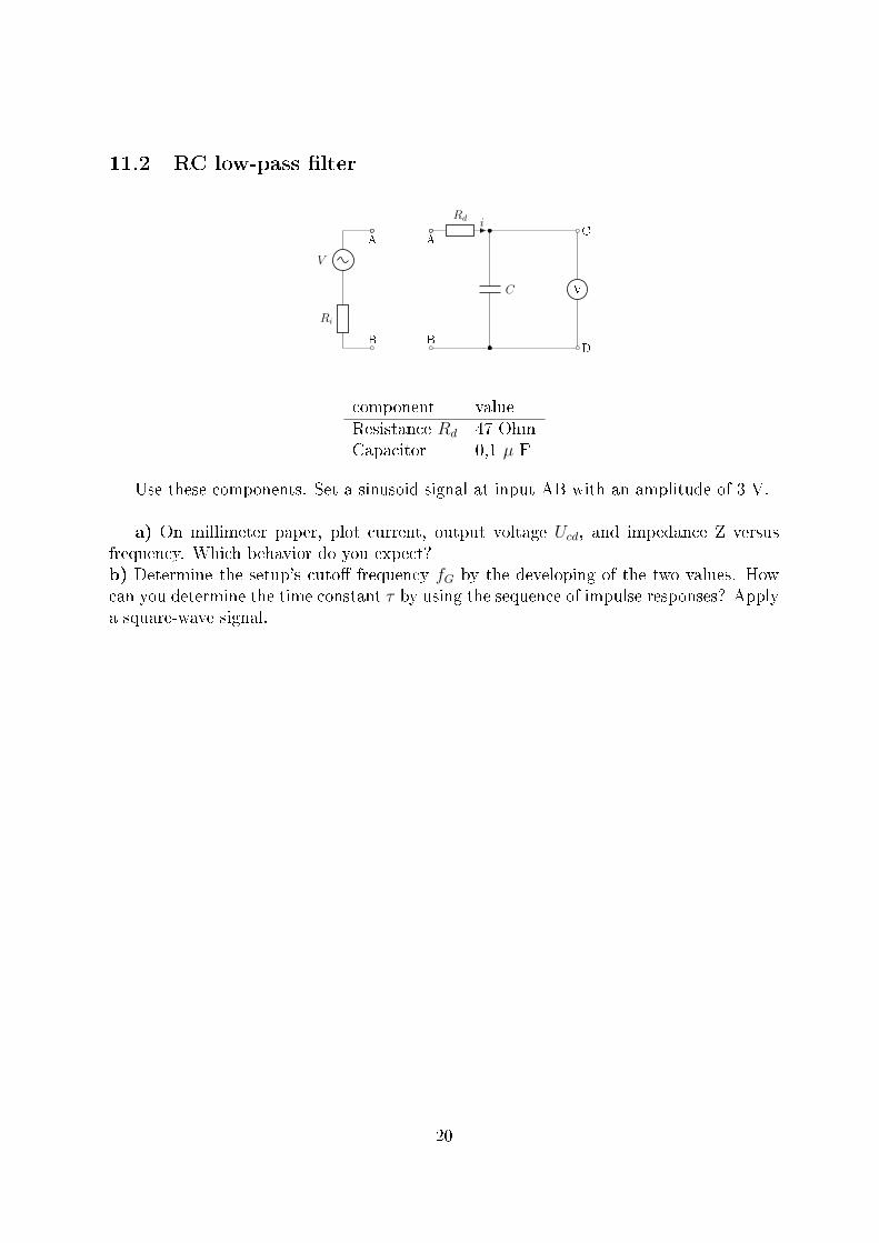
11.2 RC low-pass �lter
B
Ri
V
A
B
Rd i
C
A
D
C
V
component valueResistance Rd 47 OhmCapacitor 0,1 µ F
Use these components. Set a sinusoid signal at input AB with an amplitude of 3 V.
a) On millimeter paper, plot current, output voltage Ucd, and impedance Z versusfrequency. Which behavior do you expect?b) Determine the setup's cuto� frequency fG by the developing of the two values. Howcan you determine the time constant τ by using the sequence of impulse responses? Applya square-wave signal.
20