Embed Size (px)
Citation preview
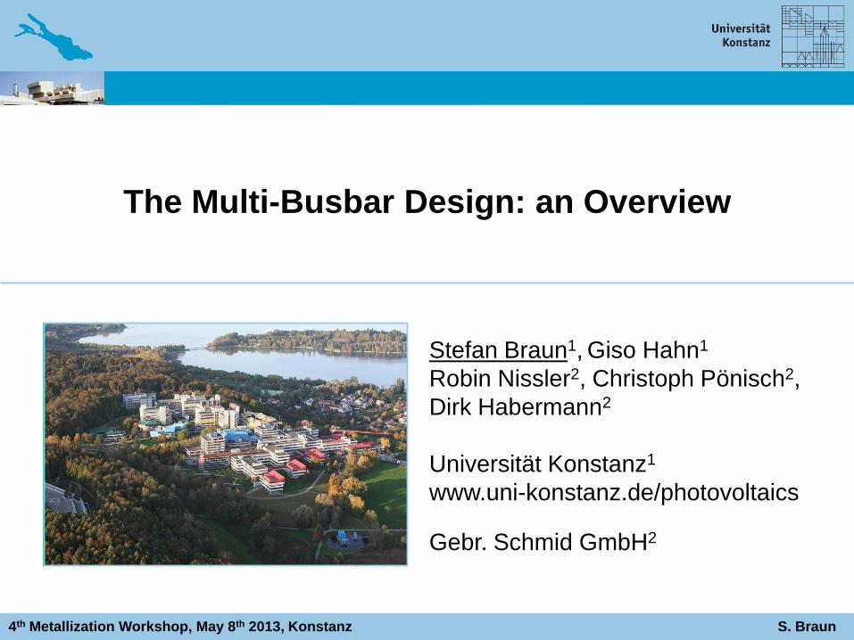
4th Metallization Workshop, May 8th 2013, Konstanz S. Braun
The Multi-Busbar Design: an Overview
Stefan Braun1, Giso Hahn1
Robin Nissler2, Christoph Pönisch2,
Dirk Habermann2
Universität Konstanz1
www.uni-konstanz.de/photovoltaics
Gebr. Schmid GmbH2
4th Metallization Workshop, May 8th 2013, Konstanz S. Braun
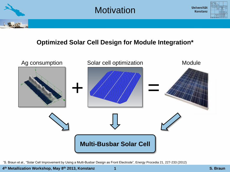
Optimized Solar Cell Design for Module Integration*
Motivation
*S. Braun et al., “Solar Cell Improvement by Using a Multi-Busbar Design as Front Electrode”, Energy Procedia 21, 227-233 (2012)
1
Multi-Busbar Solar Cell
Ag consumption Module Solar cell optimization
+ =
4th Metallization Workshop, May 8th 2013, Konstanz S. Braun
Outline
• Motivation
• Cell Concepts
- Differences between 3-busbar and multi-busbar solar cell
• Simulation
- Advantages of multi-busbar design on cell- and module-level
• Results of Experiment
- Solar cells & one cell modules
• Summary
2
4th Metallization Workshop, May 8th 2013, Konstanz S. Braun
Cell Concepts
3
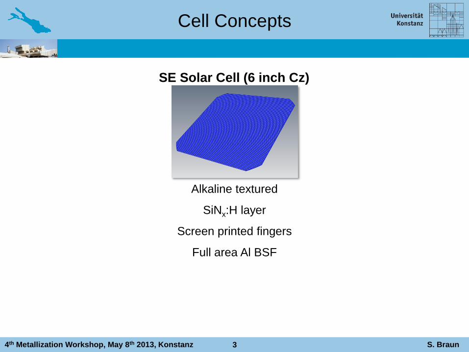
Alkaline textured
SiNx:H layer
Screen printed fingers
Full area Al BSF
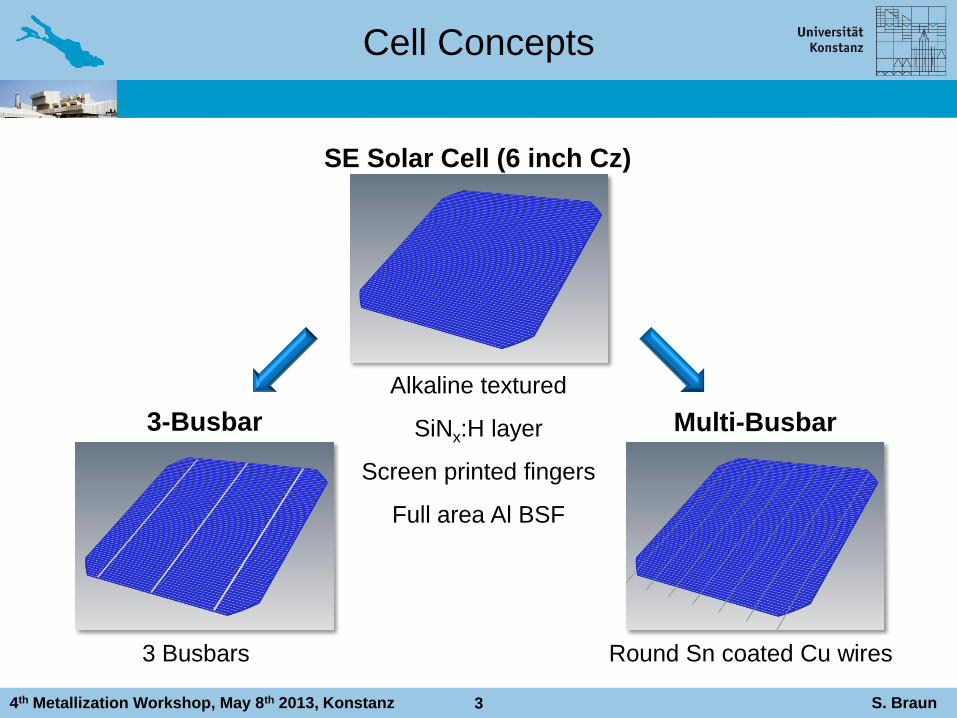
SE Solar Cell (6 inch Cz)
4th Metallization Workshop, May 8th 2013, Konstanz S. Braun
Cell Concepts
3-Busbar Multi-Busbar
3
3 Busbars Round Sn coated Cu wires
Alkaline textured
SiNx:H layer
Screen printed fingers
Full area Al BSF
SE Solar Cell (6 inch Cz)
4th Metallization Workshop, May 8th 2013, Konstanz S. Braun
Extraction IV Parameters
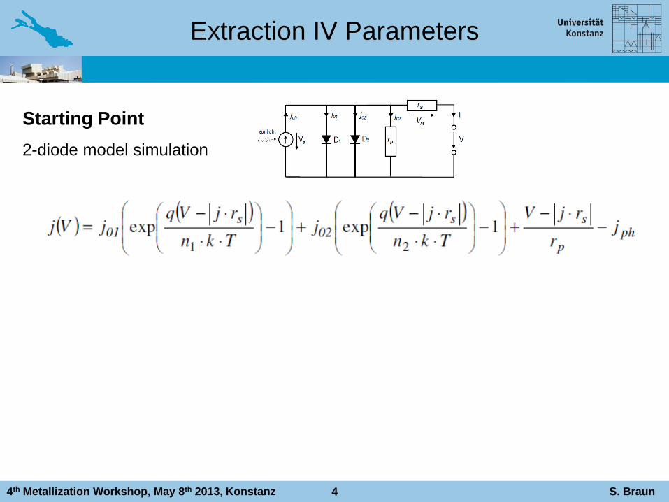
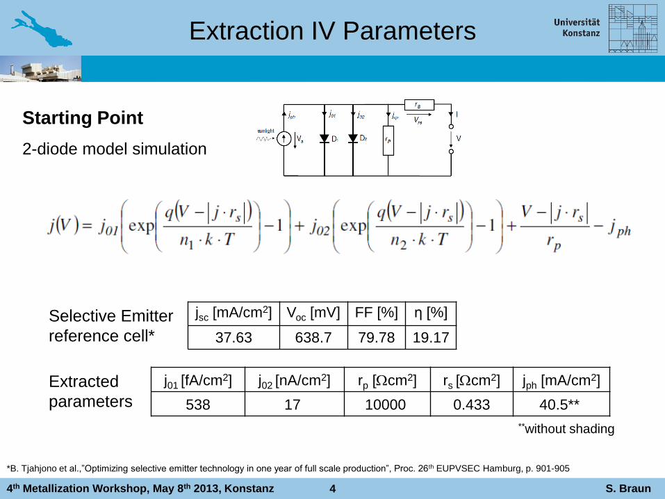
Starting Point
2-diode model simulation
4
4th Metallization Workshop, May 8th 2013, Konstanz S. Braun
Extraction IV Parameters
Starting Point
2-diode model simulation
4
jsc [mA/cm2] Voc [mV] FF [%] η [%]
37.63 638.7 79.78 19.17
*B. Tjahjono et al.,”Optimizing selective emitter technology in one year of full scale production”, Proc. 26th EUPVSEC Hamburg, p. 901-905
j01 [fA/cm2] j02 [nA/cm2] rp [cm2] rs [cm2] jph [mA/cm2]
538 17 10000 0.433 40.5**
**without shading
Selective Emitter
reference cell*
Extracted
parameters
4th Metallization Workshop, May 8th 2013, Konstanz S. Braun
Simulation
5
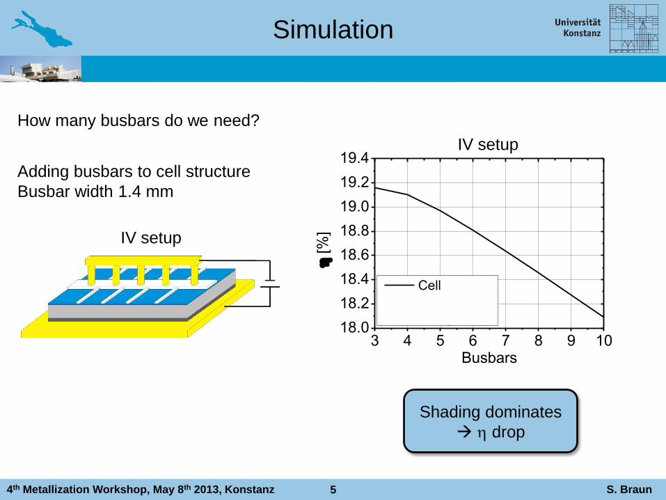
Adding busbars to cell structure
Busbar width 1.4 mm
3 4 5 6 7 8 9 1018.0
18.2
18.4
18.6
18.8
19.0
19.2
19.4
[
%]
Busbars
Cell
Stringed
Stringed opt.
How many busbars do we need?
IV setup
Shading dominates
drop
IV setup
4th Metallization Workshop, May 8th 2013, Konstanz S. Braun
Simulation
6
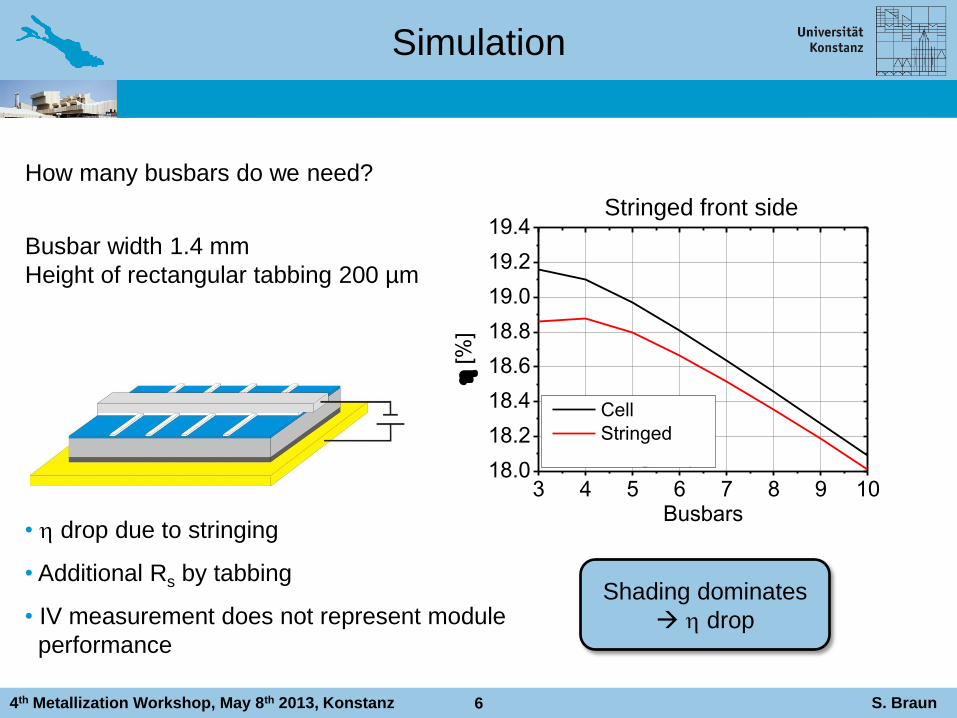
How many busbars do we need?
Busbar width 1.4 mm
Height of rectangular tabbing 200 µm
Shading dominates
drop
3 4 5 6 7 8 9 1018.0
18.2
18.4
18.6
18.8
19.0
19.2
19.4
[
%]
Busbars
Cell
Stringed
Stringed opt.
• drop due to stringing
• Additional Rs by tabbing
• IV measurement does not represent module
..performance
Stringed front side
4th Metallization Workshop, May 8th 2013, Konstanz S. Braun
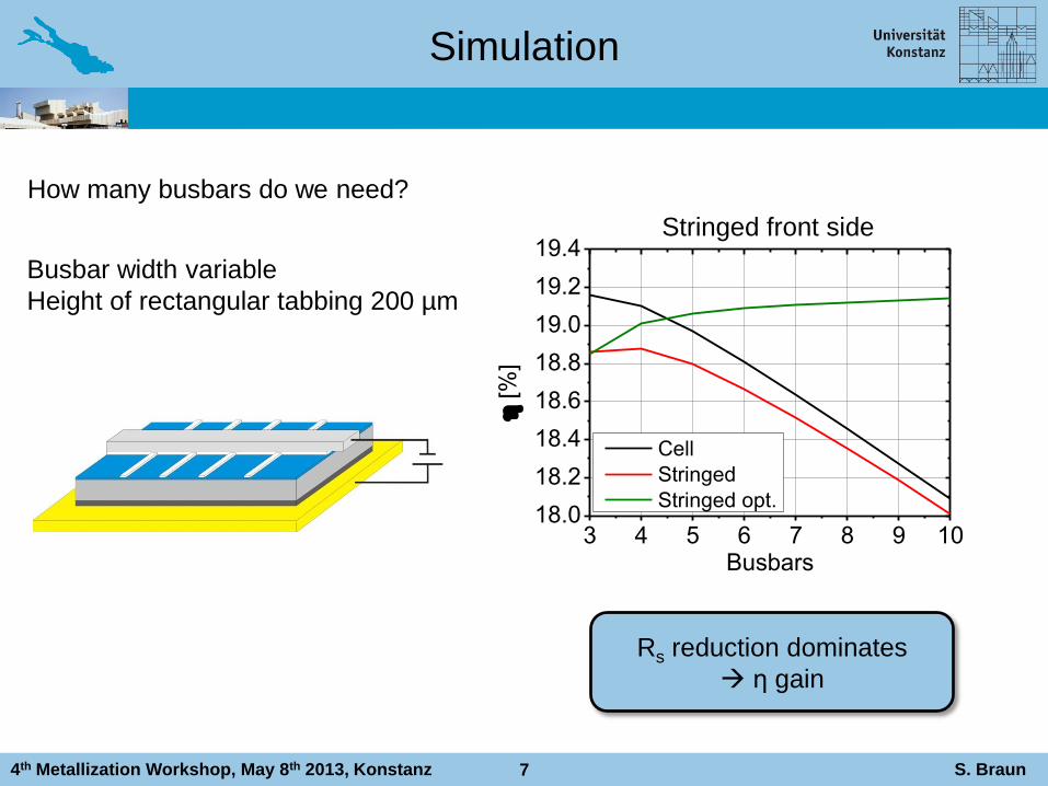
Simulation
7
Busbar width variable
Height of rectangular tabbing 200 µm
Rs reduction dominates
η gain
How many busbars do we need?
3 4 5 6 7 8 9 1018.0
18.2
18.4
18.6
18.8
19.0
19.2
19.4
[
%]
Busbars
Cell
Stringed
Stringed opt.
Stringed front side
4th Metallization Workshop, May 8th 2013, Konstanz S. Braun
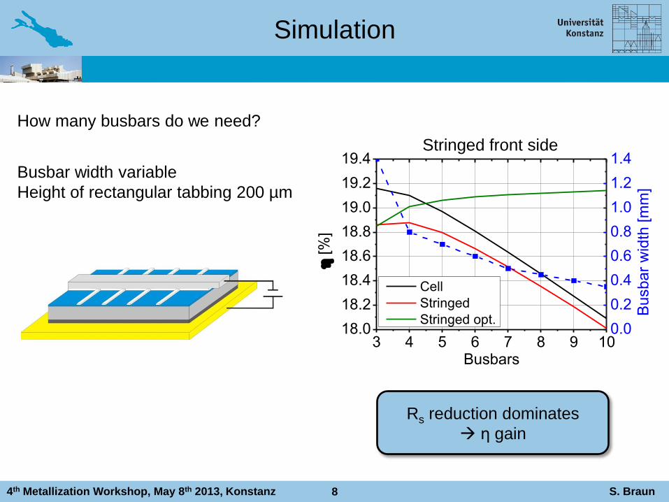
Simulation
8
How many busbars do we need?
Busbar width variable
Height of rectangular tabbing 200 µm
3 4 5 6 7 8 9 1018.0
18.2
18.4
18.6
18.8
19.0
19.2
19.4
[
%]
Busbars
Cell
Stringed
Stringed opt.0.0
0.2
0.4
0.6
0.8
1.0
1.2
1.4
Bu
sba
r w
idth
[m
m]
Stringed front side
Rs reduction dominates
η gain
4th Metallization Workshop, May 8th 2013, Konstanz S. Braun
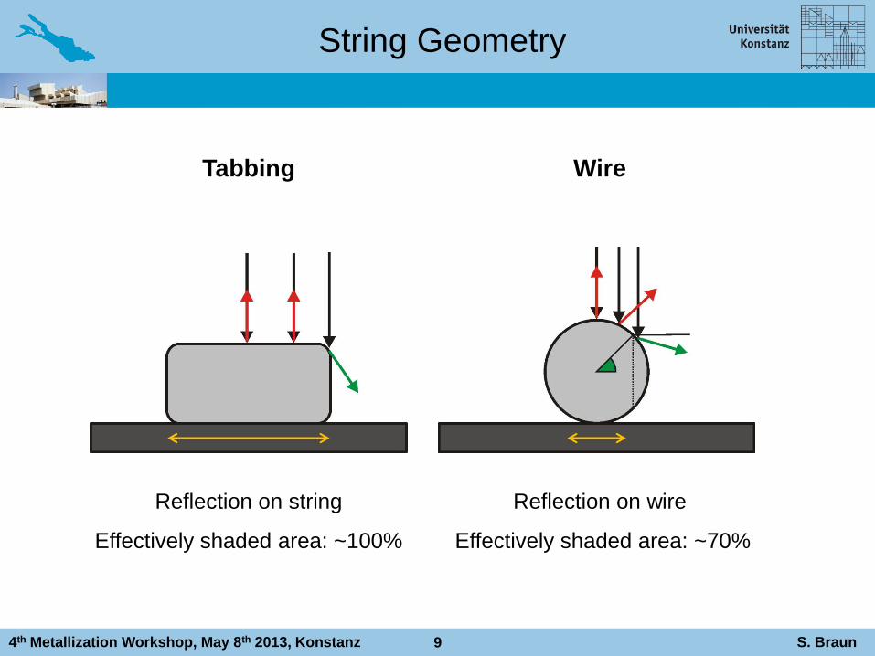
String Geometry
Tabbing
Reflection on string
Effectively shaded area: ~100%
Reflection on wire
Effectively shaded area: ~70%
Wire
9
4th Metallization Workshop, May 8th 2013, Konstanz S. Braun
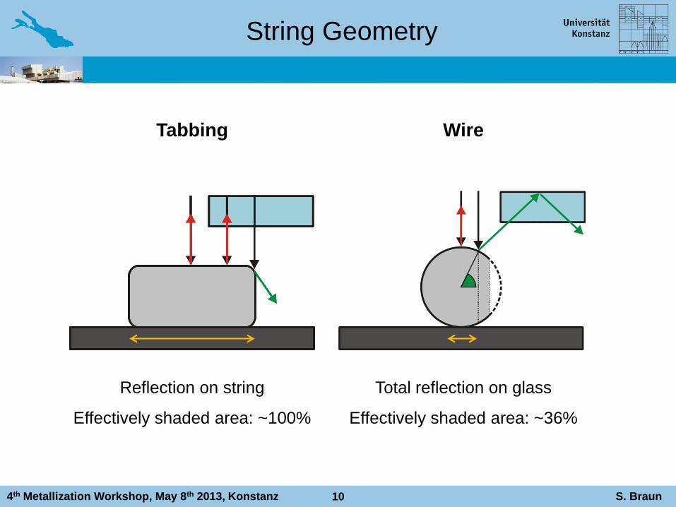
Tabbing
Total reflection on glass
Effectively shaded area: ~36%
Wire
Reflection on string
Effectively shaded area: ~100%
10
String Geometry
4th Metallization Workshop, May 8th 2013, Konstanz S. Braun
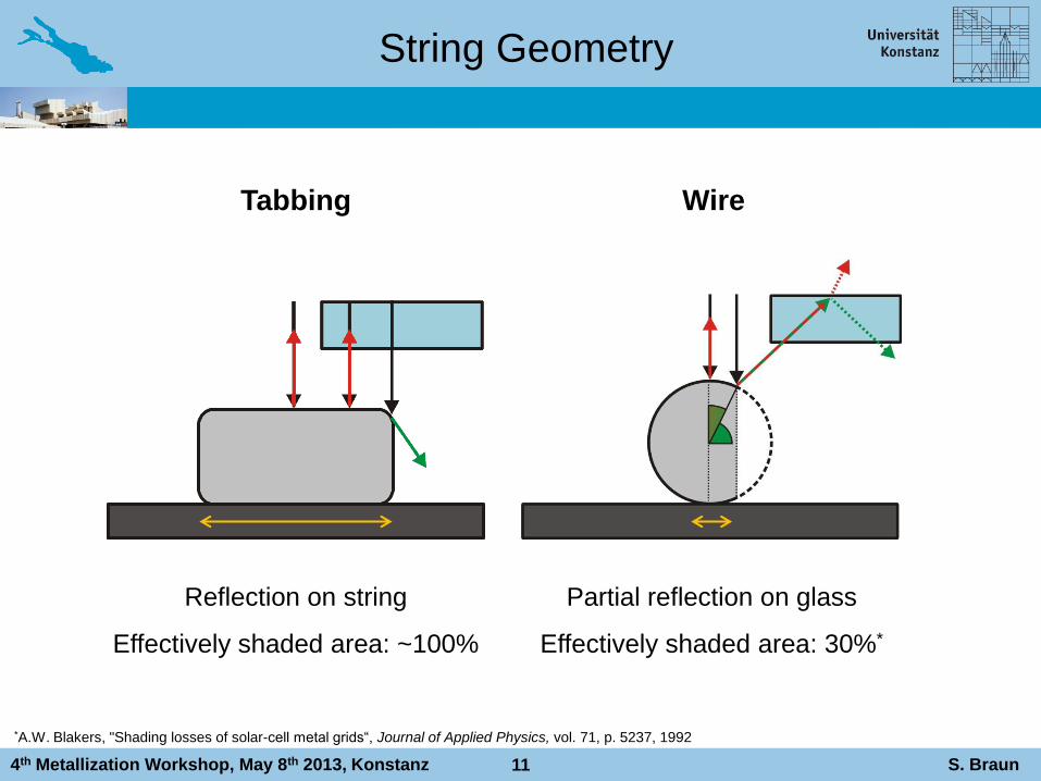
String Geometry
Tabbing
Partial reflection on glass
Effectively shaded area: 30%*
Wire
Reflection on string
Effectively shaded area: ~100%
11
*A.W. Blakers, "Shading losses of solar-cell metal grids“, Journal of Applied Physics, vol. 71, p. 5237, 1992
4th Metallization Workshop, May 8th 2013, Konstanz S. Braun
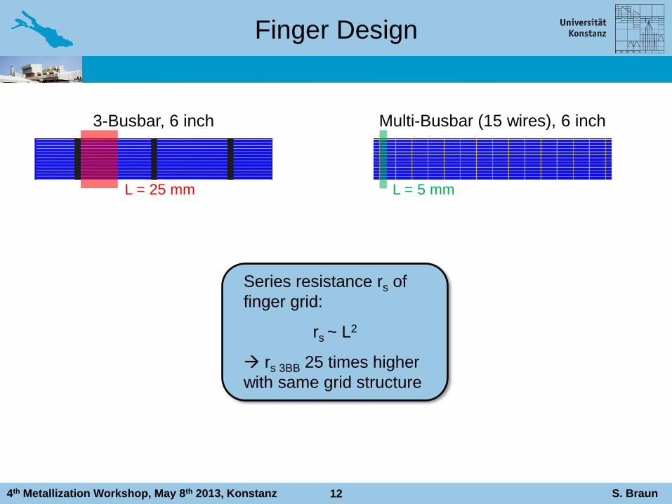
Finger Design
12
Series resistance rs of
finger grid:
rs ~ L2
rs 3BB 25 times higher
with same grid structure
L = 25 mm L = 5 mm
3-Busbar, 6 inch Multi-Busbar (15 wires), 6 inch
4th Metallization Workshop, May 8th 2013, Konstanz S. Braun
10 20 30 40 50 60 70 80 900.0
0.2
0.4
0.6
0.8
1.0
r s [
cm
2]
Finger width [µm]
3 Busbars
15 Wires
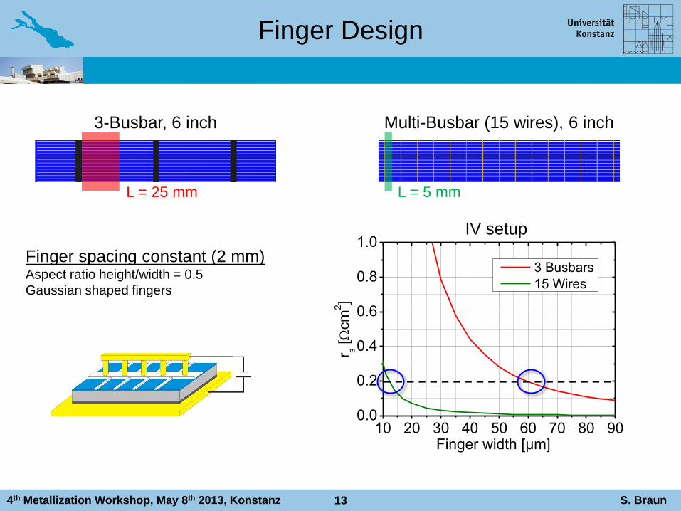
Finger Design
Finger spacing constant (2 mm) Aspect ratio height/width = 0.5
Gaussian shaped fingers
13
IV setup
L = 25 mm L = 5 mm
3-Busbar, 6 inch Multi-Busbar (15 wires), 6 inch
4th Metallization Workshop, May 8th 2013, Konstanz S. Braun
10 20 30 40 50 60 70 80 900.0
0.1
0.2
0.3
0.4
0.5
0.6
r s [
cm
2]
Finger width [µm]
3 Busbars
15 Wires
0.0
0.4
0.8
1.2
1.6
2.0
2.4
Fin
ge
r sp
acin
g [
mm
]
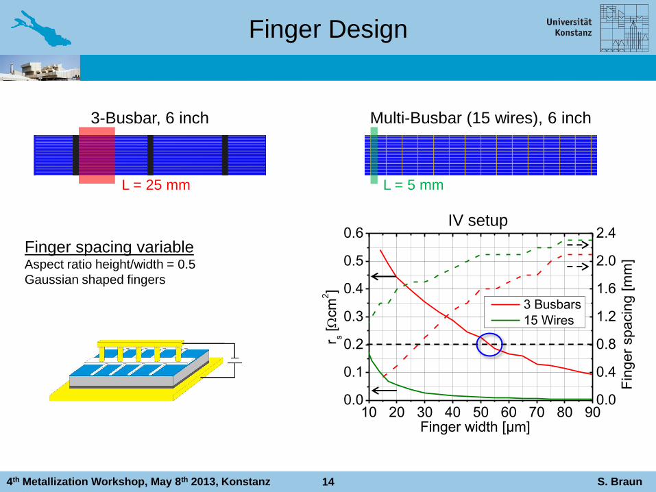
Finger Design
Finger spacing variable Aspect ratio height/width = 0.5
Gaussian shaped fingers
14
IV setup
L = 25 mm L = 5 mm
3-Busbar, 6 inch Multi-Busbar (15 wires), 6 inch
4th Metallization Workshop, May 8th 2013, Konstanz S. Braun
10 20 30 40 50 60 70 80 900.0
0.1
0.2
0.3
0.4
0.5
0.6
r s [
cm
2]
Finger width [µm]
3 Busbars
15 Wires
18.8
19.0
19.2
19.4
19.6
19.8
20.0
[%
]
IV setup
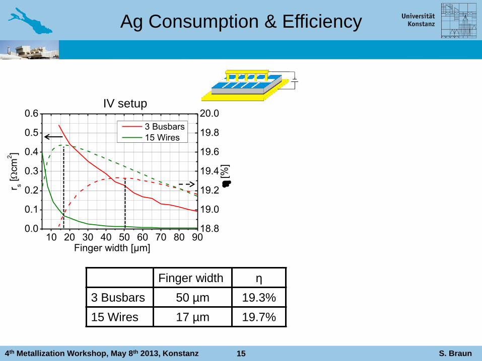
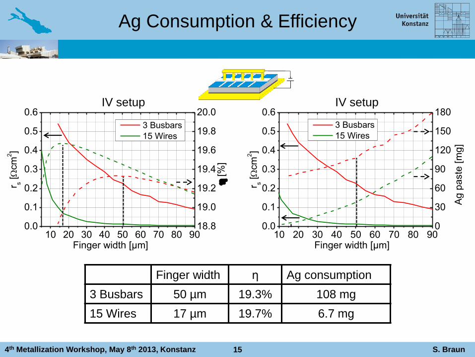
Ag Consumption & Efficiency
15
Finger width η
3 Busbars 50 µm 19.3%
15 Wires 17 µm 19.7%
4th Metallization Workshop, May 8th 2013, Konstanz S. Braun
10 20 30 40 50 60 70 80 900.0
0.1
0.2
0.3
0.4
0.5
0.6
r s [
cm
2]
Finger width [µm]
3 Busbars
15 Wires
18.8
19.0
19.2
19.4
19.6
19.8
20.0
[%
]
IV setup
10 20 30 40 50 60 70 80 900.0
0.1
0.2
0.3
0.4
0.5
0.6
r s [
cm
2]
Finger width [µm]
3 Busbars
15 Wires
0
30
60
90
120
150
180
Ag
pa
ste
[m
g]
15
Finger width η Ag consumption
3 Busbars 50 µm 19.3% 108 mg
15 Wires 17 µm 19.7% 6.7 mg
Ag Consumption & Efficiency
IV setup
4th Metallization Workshop, May 8th 2013, Konstanz S. Braun
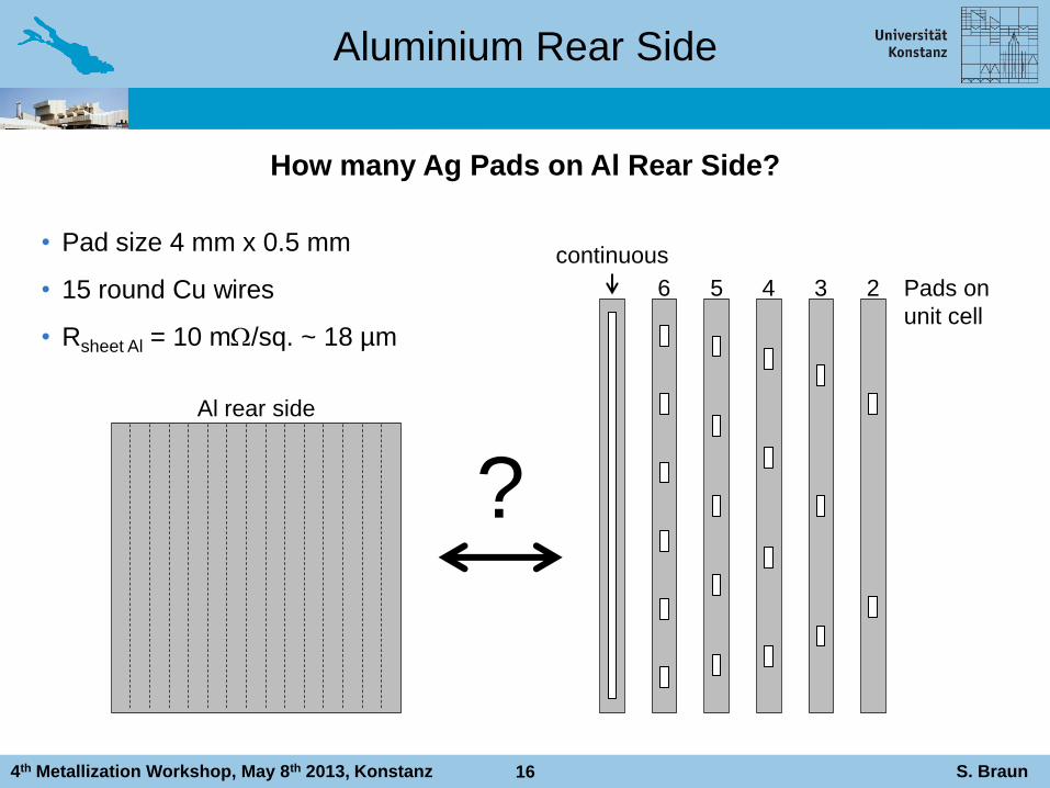
Aluminium Rear Side
• Pad size 4 mm x 0.5 mm
• 15 round Cu wires
• Rsheet Al = 10 m/sq. ~ 18 µm
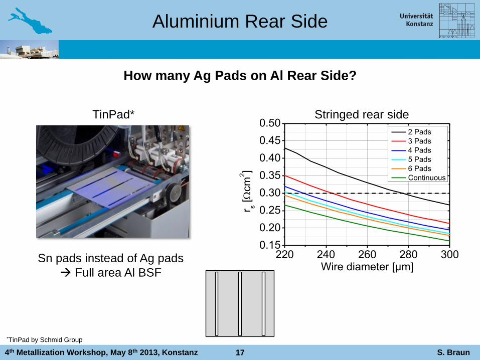
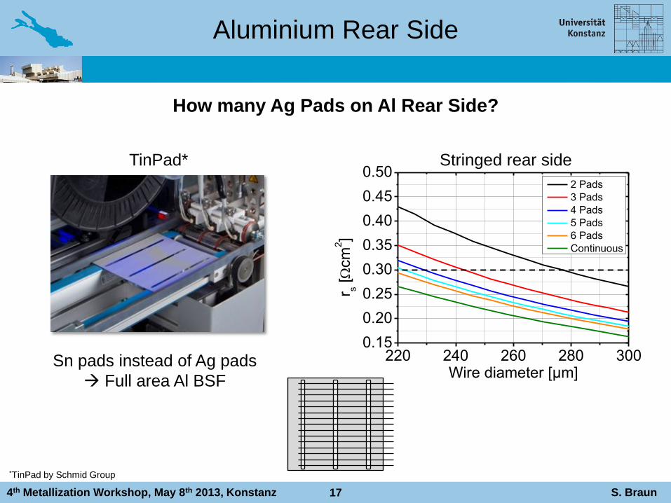
How many Ag Pads on Al Rear Side?
16
?
continuous
6 5 4 3 2 Pads on
unit cell
Al rear side
4th Metallization Workshop, May 8th 2013, Konstanz S. Braun
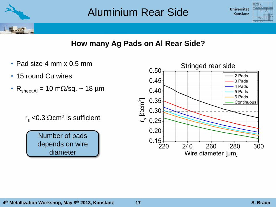
220 240 260 280 3000.15
0.20
0.25
0.30
0.35
0.40
0.45
0.50
r s [
cm
2]
Wire diameter [µm]
2 Pads
3 Pads
4 Pads
5 Pads
6 Pads
Continuous
Aluminium Rear Side
Number of pads
depends on wire
diameter
How many Ag Pads on Al Rear Side?
17
Stringed rear side
rs <0.3 cm2 is sufficient
• Pad size 4 mm x 0.5 mm
• 15 round Cu wires
• Rsheet Al = 10 m/sq. ~ 18 µm
4th Metallization Workshop, May 8th 2013, Konstanz S. Braun
220 240 260 280 3000.15
0.20
0.25
0.30
0.35
0.40
0.45
0.50
r s [
cm
2]
Wire diameter [µm]
2 Pads
3 Pads
4 Pads
5 Pads
6 Pads
Continuous
Aluminium Rear Side
17
How many Ag Pads on Al Rear Side?
*TinPad by Schmid Group
TinPad*
Sn pads instead of Ag pads
Full area Al BSF
Stringed rear side
4th Metallization Workshop, May 8th 2013, Konstanz S. Braun
Aluminium Rear Side
17
How many Ag Pads on Al Rear Side?
*TinPad by Schmid Group
220 240 260 280 3000.15
0.20
0.25
0.30
0.35
0.40
0.45
0.50
r s [
cm
2]
Wire diameter [µm]
2 Pads
3 Pads
4 Pads
5 Pads
6 Pads
Continuous
Stringed rear side TinPad*
Sn pads instead of Ag pads
Full area Al BSF
4th Metallization Workshop, May 8th 2013, Konstanz S. Braun
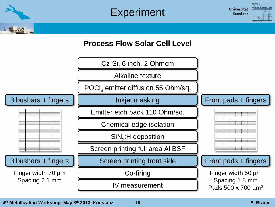
Experiment
Process Flow Solar Cell Level
Alkaline texture
Emitter etch back 110 Ohm/sq.
POCl3 emitter diffusion 55 Ohm/sq.
Inkjet masking
Cz-Si, 6 inch, 2 Ohmcm
Chemical edge isolation
SiNx:H deposition
Screen printing full area Al BSF
Screen printing front side
Co-firing
3 busbars + fingers Front pads + fingers
3 busbars + fingers Front pads + fingers
IV measurement
18
Finger width 70 µm
Spacing 2.1 mm
Finger width 50 µm
Spacing 1.8 mm
Pads 500 x 700 µm2
4th Metallization Workshop, May 8th 2013, Konstanz S. Braun
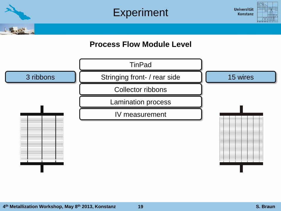
Experiment
Process Flow Module Level
19
Stringing front- / rear side
IV measurement
Collector ribbons
Lamination process
TinPad
3 ribbons 15 wires
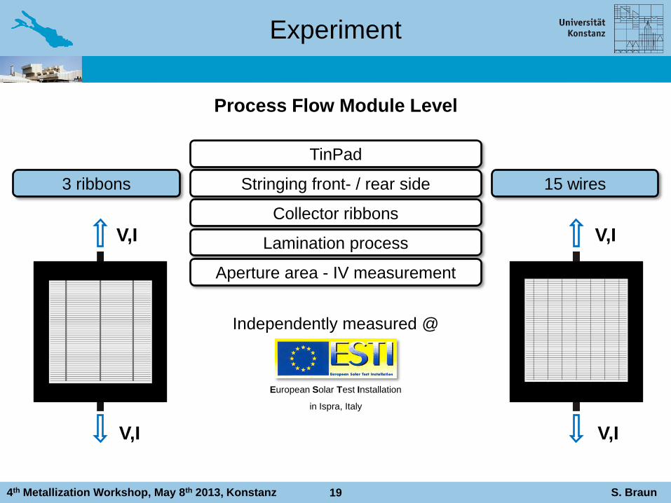
4th Metallization Workshop, May 8th 2013, Konstanz S. Braun
Experiment
Process Flow Module Level
V,I
V,I
V,I
V,I
European Solar Test Installation
in Ispra, Italy
19
Stringing front- / rear side
Aperture area - IV measurement
Collector ribbons
Lamination process
TinPad
3 ribbons 15 wires
Independently measured @
4th Metallization Workshop, May 8th 2013, Konstanz S. Braun
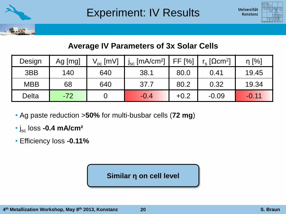
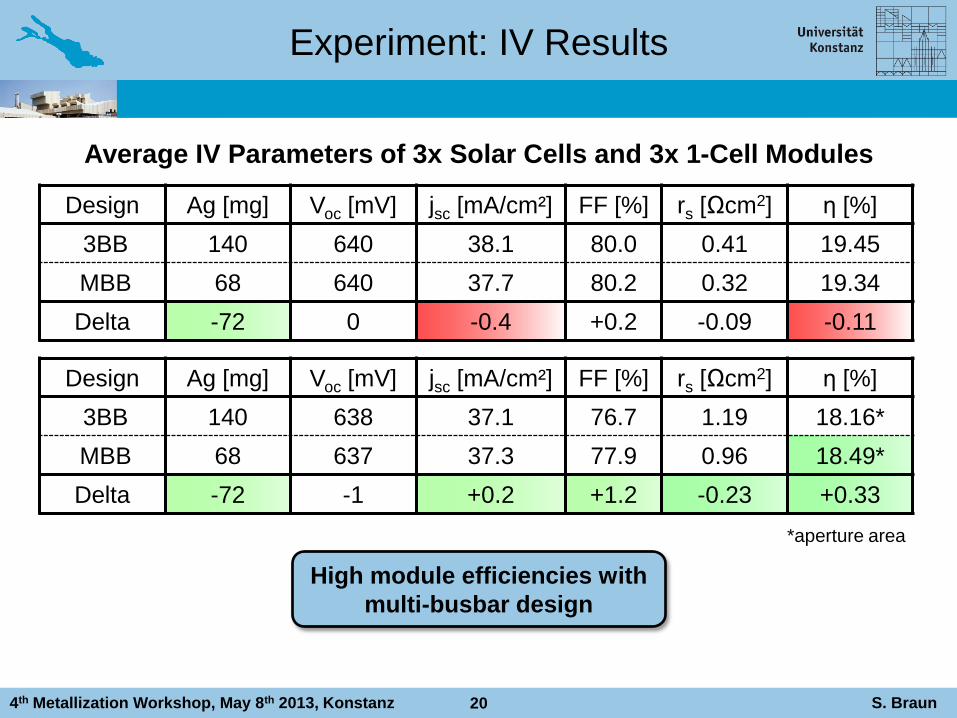
Experiment: IV Results
Design Ag [mg] Voc [mV] jsc [mA/cm²] FF [%] rs [Ωcm2] η [%]
3BB 140 640 38.1 80.0 0.41 19.45
MBB 68 640 37.7 80.2 0.32 19.34
Delta -72 0 -0.4 +0.2 -0.09 -0.11
Average IV Parameters of 3x Solar Cells
20
• Ag paste reduction >50% for multi-busbar cells (72 mg)
• jsc loss -0.4 mA/cm²
• Efficiency loss -0.11%
Similar η on cell level
4th Metallization Workshop, May 8th 2013, Konstanz S. Braun
Experiment: IV Results
Average IV Parameters of 3x Solar Cells and 3x 1-Cell Modules
20
Design Ag [mg] Voc [mV] jsc [mA/cm²] FF [%] rs [Ωcm2] η [%]
3BB 140 638 37.1 76.7 1.19 18.16*
MBB 68 637 37.3 77.9 0.96 18.49*
Delta -72 -1 +0.2 +1.2 -0.23 +0.33
High module efficiencies with
multi-busbar design
*aperture area
Design Ag [mg] Voc [mV] jsc [mA/cm²] FF [%] rs [Ωcm2] η [%]
3BB 140 640 38.1 80.0 0.41 19.45
MBB 68 640 37.7 80.2 0.32 19.34
Delta -72 0 -0.4 +0.2 -0.09 -0.11
4th Metallization Workshop, May 8th 2013, Konstanz S. Braun
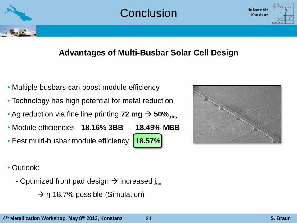
• Multiple busbars can boost module efficiency
• Technology has high potential for metal reduction
• Ag reduction via fine line printing 72 mg 50%abs
• Module efficiencies 18.16% 3BB 18.49% MBB
• Best multi-busbar module efficiency 18.57%
• Outlook:
- Optimized front pad design increased jsc
η 18.7% possible (Simulation)
Conclusion
Advantages of Multi-Busbar Solar Cell Design
21
4th Metallization Workshop, May 8th 2013, Konstanz S. Braun
Thank you for your attention!
Special thanks to: Schmid Group for funding
Harald Müllejans, Diego Pavanello, Elena Salis, Roberto Galleano for IV measurements