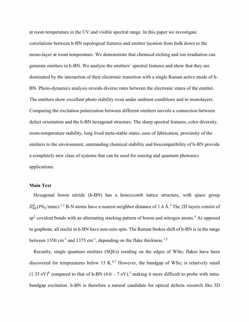
Embed Size (px)
Citation preview
Topological attributes and photo-dynamics of visible
spectrum quantum emitters in hexagonal boron
nitride
Nathan Chejanovsky 1,2, Mohammad Rezai 1, Federico Paolucci 2 , Youngwook Kim 2, Torsten
Rendler 1, Wafa Rouabeh 2, Felipe Fávaro de Oliveira 1, Patrick Herlinger 2, Andrej
Denisenko 1, Sen Yang 1, Ilja Gerhardt 1,2, Amit Finkler* 1, Jurgen H. Smet 2 and Jörg Wrachtrup
1,2
1 3. Physikalisches Institut, Universität Stuttgart, Pfaffenwaldring 57, 70569 Stuttgart, Germany
2 Max Planck Institute for Solid State Research, Heisenbergstr. 1, 70569 Stuttgart, Germany
Keywords: single quantum emitters, hexagonal boron-nitride, van der Waals materials
Abstract
Newly discovered van der Waals materials like MoS2, WSe2, hexagonal boron nitride (h-BN)
and recently C2N have sparked intensive research to unveil the quantum behavior associated with
their 2D topology. Of great interest are 2D materials that host single quantum emitters. h-BN,
with a band-gap of 4.6 - 7 eV, has been shown to host single quantum emitters which are stable
at room temperature in the UV and visible spectral range. In this paper we investigate
correlations between h-BN topological features and emitter location from bulk down to the
mono-layer at room temperature. We demonstrate that chemical etching and ion irradiation can
generate emitters in h-BN. We analyze the emitters’ spectral features and show that they are
dominated by the interaction of their electronic transition with a single Raman active mode of h-
BN. Photo-dynamics analysis reveals diverse rates between the electronic states of the emitter.
The emitters show excellent photo stability even under ambient conditions and in monolayers.
Comparing the excitation polarization between different emitters unveils a connection between
defect orientation and the h-BN hexagonal structure. The sharp spectral features, color diversity,
room-temperature stability, long lived meta-stable states, ease of fabrication, proximity of the
emitters to the environment, outstanding chemical stability and biocompatibility of h-BN provide
a completely new class of systems that can be used for sensing and quantum photonics
applications.
Main Text
Hexagonal boron nitride (h-BN) has a honeycomb lattice structure, with space group
𝐷4ℎ6 (𝑃63/mmc).1,2 B-N atoms have a nearest neighbor distance of 1.4 Å.3 The 2D layers consist of
sp2 covalent bonds with an alternating stacking pattern of boron and nitrogen atoms.4 As opposed
to graphene, all nuclei in h-BN have non-zero spin. The Raman Stokes shift of h-BN is in the range
between 1350 cm-1 and 1375 cm-1, depending on the flake thickness.1,5
Recently, single quantum emitters (SQEs) residing on the edges of WSe2 flakes have been
discovered for temperatures below 15 K.6,7 However, the bandgap of WSe2 is relatively small
(1.35 eV)8 compared to that of h-BN (4.6 – 7 eV),3 making it more difficult to probe with intra-
bandgap excitation. h-BN is therefore a natural candidate for optical defects research like 3D
materials that host optical defects, such as diamond which hosts e.g. the nitrogen-vacancy (NV)
center. 9 A major difference, however, is that because of the 2D nature of h-BN, a defect would be
closer to the external environment. This results in a heterogeneous environment in which a defect
in h-BN resides. As a consequence, we expect the photoluminescence (PL) spectrum, lifetimes
and other related phenomena to reflect this heterogeneity.
h-BN has been widely studied for its emission in the UV spectral range 10 and was recently
proven to have an indirect bandgap.11 Exciton UV emission in the ~220 nm spectral range has been
attributed to grain boundaries and dislocations 12 and, using cathodoluminescence, for stacking
faults localized at fold crossings of the flakes, resulting in local symmetry changes.13 For the ~300
nm range, nitrogen vacancies and carbon impurities have been ascribed as the source of
emission.14,15
Recently, it was demonstrated that h-BN also hosts SQEs in the UV 16 as well as the visible
range (623 nm).17 The defect thought responsible for quantum emission at 623 nm was an anti-site
complex, i.e. a nitrogen occupies the boron site with a missing atom at the nitrogen site, 𝑁𝐵𝑉𝑁.
The high density of emitters found,17 in account with the fact that due to the 2D nature of h-BN
the emitters are exposed to the environment, suggests that sample preparation should have a
significant influence on its behavior.
In this paper we show two possible methods that can be used in order to create QEs in h-BN
utilizing chemical etching and ion irradiation. We probe the QEs using 532 nm green laser and
594 nm orange laser, which should assist in exciting inside the band-gap and thus avoiding
excitonic emission. We analyze the spectral behavior of numerous cases of QE from different
sources from bulk down to the mono-layer and show the similarity between them and an
orientational correlation to the structure of h-BN. An analysis of photo-dynamics reveals a
complex picture, which can hint to the presence of charge states. From these methods and previous
research, we try to deduce the possible origin of the SQEs involved. Our results suggest that SQE
topological and transition rate behavior have a connection to the reduced dimensionality of h-BN
and our analysis points to a possible link between perimeters and defect formation.
We investigate h-BN from several sources: exfoliated flakes, purchased mono-layer CVD h-BN
(Graphene supermarket) and in-house grown CVD h-BN, comparing topological, spectral and
autocorrelation similarities between them. Measurements were performed on SiO2 substrates. For
the exfoliated h-BN we also tested a diamond substrate - to exclude substrate contributions to the
SQEs. Some of our SiO2 substrates were etched with patterned holes to suspended h-BN flakes in
order to avoid interaction with the surface. A microscope image is given in Fig. 1a.
In addition to testing various sample sources we also performed two treatments on the exfoliated
h-BN flakes to generate defects.
Firstly, two chemical etching methods were tested on exfoliated flakes, which thin down the
flakes and proved important for generating single emitters. The first method makes use of
peroxymonosulfuric acid (H2O2:H2SO4), which can be tuned by changing the ratio to effect a slow
rate etching of h-BN.18 This is similar to standard methods that are used for diamond cleaning for
use of the NV- defect. The second chemical etching method is based on the first one but with an
additional step of phosphoric (H3PO4) and sulfuric acids (H2SO4). This additional step can thin
down the h-BN flake at a slow and controllable rate 19 (see SI for further details). Secondly, we
irradiate the flakes with He and N ions to generate lattice vacancies, similar to procedures known
from 3D materials.
All measurements were performed with a room temperature confocal setup where photon
emission was recorded with two avalanche photo diodes (APDs) in a Hanbury Brown & Twiss
configuration. The majority of confocal scans were done with a 532 nm continuous wave (CW)
laser with a 550 nm long pass (550LP) filter. We limited our measurements to the low power
density regime of 150 µW/µm2. In addition, we also recorded images with low laser power (nW)
without any filters in order to gain insight to the correlation between emitter location and the flake
topology. In this very low laser power regime, emitters cannot be excited efficiently (as will be
shown below), which allows us to see the topological features of the flake on the area in which
they are embedded when scanning a confocal image.
We observed that prolonged (4 hours or more) exposure to the 532 nm excitation laser (in the
high power range ~ mW) can cause blinking emitters to restore to a stable emission state (not
shown). However, this method was inefficient and the mechanism behind it is unclear, perhaps
due to local heating that can have a chemical bonding effect. Furthermore, annealing proved to be
a crucial step for emitter stability in order to avoid working with blinking emitters and
consequently for all flakes in this manuscript (treated and un-treated) we annealed the samples.
The majority of samples were thermally annealed using the procedure described in Ref. 17 – under
an argon environment at 850 °C.
In the following we first discuss our methods to generate quantum emitters in h-BN and then
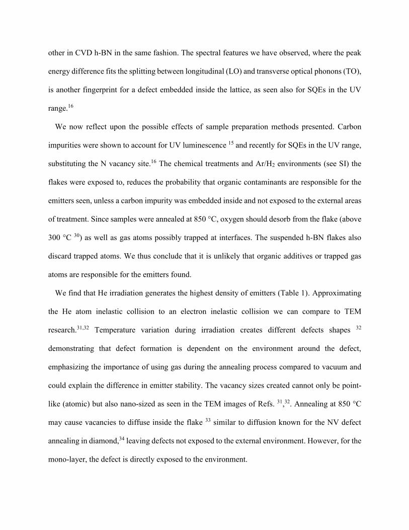
proceed to spectral and transition rate analysis of the QEs. We first measured h-BN flakes
suspended over a hole in the substrate, confirming the presence of h-BN using Raman spectroscopy
(Fig. 1a). Fig. 1b upper/lower shows an unfiltered/filtered (respectively) confocal image of an area
of the flake in Fig. 1a. suspended over a hole (hole marked as a purple circle in Fig. 1b). A
suspended emitter can be seen in this area (marked in a red circle) in the depth (Z) and lateral (XY)
scan. Thus, quantum emitters are not localized on the interfaces between the h-BN flakes and the
substrate, but are an intrinsic property of the suspended flake. On the exfoliated flakes we see
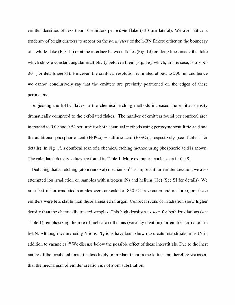
emitter densities of less than 10 emitters per whole flake (~30 µm lateral). We also notice a
tendency of bright emitters to appear on the perimeters of the h-BN flakes: either on the boundary
of a whole flake (Fig. 1c) or at the interface between flakes (Fig. 1d) or along lines inside the flake
which show a constant angular multiplicity between them (Fig. 1e), which, in this case, is 𝛼 ~ 𝑛 ∙
30° (for details see SI). However, the confocal resolution is limited at best to 200 nm and hence
we cannot conclusively say that the emitters are precisely positioned on the edges of these
perimeters.
Subjecting the h-BN flakes to the chemical etching methods increased the emitter density
dramatically compared to the exfoliated flakes. The number of emitters found per confocal area
increased to 0.09 and 0.54 per µm2 for both chemical methods using peroxymonosulfuric acid and
the additional phosphoric acid (H3PO4) + sulfuric acid (H2SO4), respectively (see Table 1 for
details). In Fig. 1f, a confocal scan of a chemical etching method using phosphoric acid is shown.
The calculated density values are found in Table 1. More examples can be seen in the SI.
Deducing that an etching (atom removal) mechanism18 is important for emitter creation, we also
attempted ion irradiation on samples with nitrogen (N) and helium (He) (See SI for details). We
note that if ion irradiated samples were annealed at 850 °C in vacuum and not in argon, these
emitters were less stable than those annealed in argon. Confocal scans of irradiation show higher
density than the chemically treated samples. This high density was seen for both irradiations (see
Table 1), emphasizing the role of inelastic collisions (vacancy creation) for emitter formation in
h-BN. Although we are using N ions, N2 ions have been shown to create interstitials in h-BN in
addition to vacancies.20 We discuss below the possible effect of these interstitials. Due to the inert
nature of the irradiated ions, it is less likely to implant them in the lattice and therefore we assert
that the mechanism of emitter creation is not atom substitution.
Next, we investigated defects in mono-layers. To that end we compared the topological features
and density of emitters in purchased mono-layer CVD h-BN to exfoliated flakes and to treated
(chemical etched/ion irradiated) flakes. CVD h-BN is typically grown on a Cu foil substrate, where
the first mono-layer growth mode is layer-by layer and afterwards changes to island on layer. 21
An SEM image of CVD mono-layer h-BN reveals non-uniform coverage already on a 20 μm scale
(see SI). We use the same transfer method procedure described in Ref. 17 also on a 180 μm thick
SiO2 with patterned holes for commercially available graphene supermarket h-BN. Probing the
sample with a 532 nm CW laser immediately reveals that emitter density (Fig. 1g) is larger than
for chemically treated flakes, but lower than for high dose ion irradiated samples. Considering the
inhomogeneous h-BN coverage on the Cu foil observed in the SEM image with our observations
on the untreated and treated (chemical etched/ion irradiated) flakes, we correlate the high density
of emitters with the large number of perimeters appearing in a CVD mono-layers due to the growth
mechanism.
In Table 1 we summarize the h-BN types/methods for increasing emitter density.
Table 1. Summary of Types/Methods for emitter generation the dependency for each method and
relative density of emitters per µm2.
Type/
Method
Exfoliation Chemical etching CVD
mono-
layer
Ion implantation
H2O2:H2
SO4 additional
H2SO4:H3PO4
He N
Low
Dose
High
Dose
Low Dose
Density
[𝝁𝒎−𝟐]
532 nm
Excitation
< ~10 emitters
per flake
(lateral ~ 30
µm)
0.09 0.57 0.64 0.59 0.73 0.73
Density
[𝝁𝒎−𝟐]
594 nm
Excitation
----- ----- ----- 0.37 ----- ----- -----
Densities are calculated for areas that showed the maximum number of emitters on a flake, a
minimum distance of 0.5 𝜇𝑚 between emitters was taken into account.
We now discuss the spectral and autocorrelation properties of the various h-BN types and show
that the spectral features resemble each other.
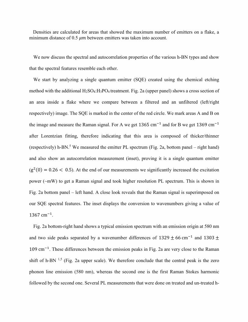
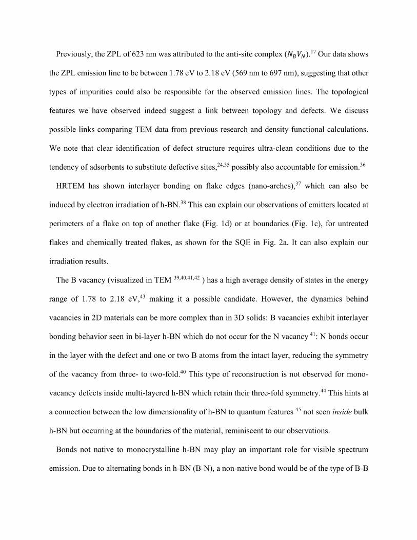
We start by analyzing a single quantum emitter (SQE) created using the chemical etching
method with the additional H2SO4:H3PO4 treatment. Fig. 2a (upper panel) shows a cross section of
an area inside a flake where we compare between a filtered and an unfiltered (left/right
respectively) image. The SQE is marked in the center of the red circle. We mark areas A and B on
the image and measure the Raman signal. For A we get 1365 cm−1 and for B we get 1369 cm−1
after Lorentzian fitting, therefore indicating that this area is composed of thicker/thinner
(respectively) h-BN.5 We measured the emitter PL spectrum (Fig. 2a, bottom panel – right hand)
and also show an autocorrelation measurement (inset), proving it is a single quantum emitter
(g2(0) = 0.26 < 0.5). At the end of our measurements we significantly increased the excitation
power (~mW) to get a Raman signal and took higher resolution PL spectrum. This is shown in
Fig. 2a bottom panel – left hand. A close look reveals that the Raman signal is superimposed on
our SQE spectral features. The inset displays the conversion to wavenumbers giving a value of
1367 cm−1.
Fig. 2a bottom-right hand shows a typical emission spectrum with an emission origin at 580 nm
and two side peaks separated by a wavenumber differences of 1329 ± 66 cm−1 and 1303 ±
109 cm−1. These differences between the emission peaks in Fig. 2a are very close to the Raman
shift of h-BN 1,5 (Fig. 2a upper scale). We therefore conclude that the central peak is the zero
phonon line emission (580 nm), whereas the second one is the first Raman Stokes harmonic
followed by the second one. Several PL measurements that were done on treated and un-treated h-
BN samples have shown that this double peak structure appears on all emitters that exhibit
quantum emission traits. However, the third peak is not always prominent enough to be seen.
Fig. 2c shows 6 PL spectra taken from QE on diamond and SiO2 substrates, emphasizing that
although emitters occur at different wavelengths, the double peak structure is recurring and is not
substrate dependent. Polarized in-plane modes for h-BN at the Γ,M and K Brillouin points should
have an energy of ~170 meV for both the transverse and longitudinal optical phonons (TO and LO
modes), whereas polarization along the c axis is expected for energies below 100 meV.2 The
spectral difference in the emission origin can arise from strain (shown for SQEs in WSe2 over a
range of 170 meV 22), different dielectric environments and most probably from at least two types
of defects or different charge states for the same defect - we discuss later in detail the possible
causes. We find a minimum full width half maximum (FWHM, denoted as ν) of 3.96 nm on the
PL spectra for non-monolayer flakes.
We perform a similar analysis on 23 adjacent peaks from various sources of h-BN (CVD mono-
layer h-BN, treated (chemically/irradiated) and un-treated emitters). We plot the difference
between adjacent peaks in wavenumbers as a function of standard deviation (Fig. 2b). The majority
of wavenumbers are located close to the value of 1363 cm-1 with an average value of 1337.6 cm-1,
very close to that of h-BN (1350 cm-1 to 1375 cm-1 depending on flake thickness).5 We therefore
show that the electron interacts with bulk or flake phonon modes rather than with localized
vibrational modes as it is the case for defects which do comprise impurity atoms with mass
significantly different from atoms of the host lattice. This spectral behavior was seen also for
defects in h-BN that emit in the UV range.10 The energy difference between the peaks fits the
splitting between LO and TO optical phonons.2
Ion irradiation produced similar spectral features like those in Fig. 2a, see SI for details.
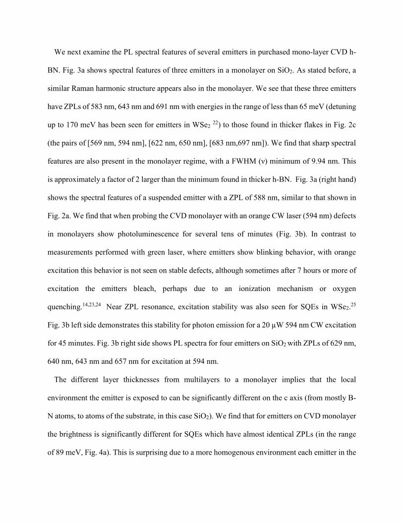
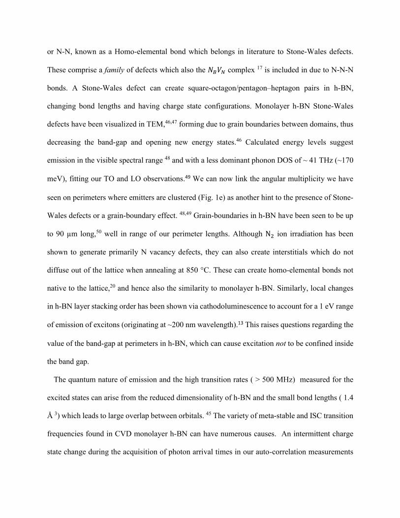
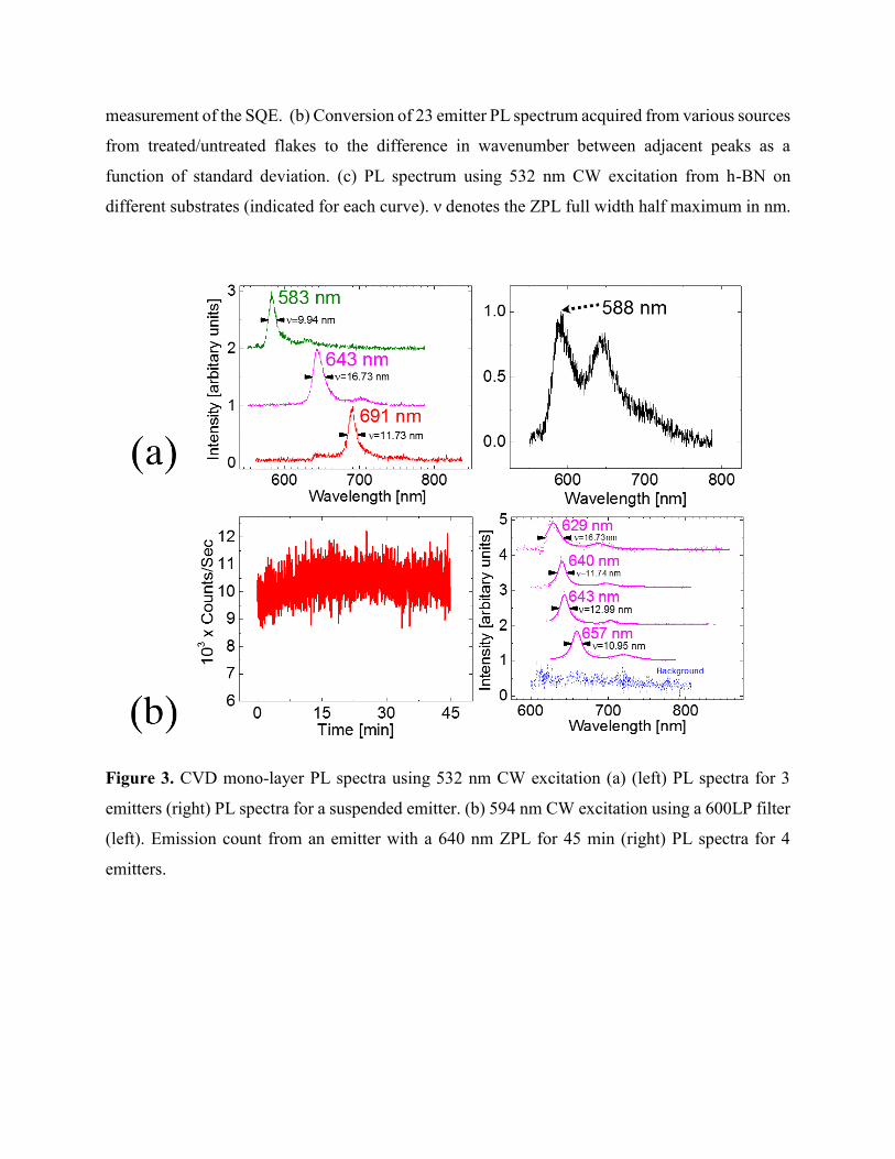
We next examine the PL spectral features of several emitters in purchased mono-layer CVD h-
BN. Fig. 3a shows spectral features of three emitters in a monolayer on SiO2. As stated before, a
similar Raman harmonic structure appears also in the monolayer. We see that these three emitters
have ZPLs of 583 nm, 643 nm and 691 nm with energies in the range of less than 65 meV (detuning
up to 170 meV has been seen for emitters in WSe2 22) to those found in thicker flakes in Fig. 2c
(the pairs of [569 nm, 594 nm], [622 nm, 650 nm], [683 nm,697 nm]). We find that sharp spectral
features are also present in the monolayer regime, with a FWHM (ν) minimum of 9.94 nm. This
is approximately a factor of 2 larger than the minimum found in thicker h-BN. Fig. 3a (right hand)
shows the spectral features of a suspended emitter with a ZPL of 588 nm, similar to that shown in
Fig. 2a. We find that when probing the CVD monolayer with an orange CW laser (594 nm) defects
in monolayers show photoluminescence for several tens of minutes (Fig. 3b). In contrast to
measurements performed with green laser, where emitters show blinking behavior, with orange
excitation this behavior is not seen on stable defects, although sometimes after 7 hours or more of
excitation the emitters bleach, perhaps due to an ionization mechanism or oxygen
quenching.14,23,24 Near ZPL resonance, excitation stability was also seen for SQEs in WSe2.25
Fig. 3b left side demonstrates this stability for photon emission for a 20 µW 594 nm CW excitation
for 45 minutes. Fig. 3b right side shows PL spectra for four emitters on SiO2 with ZPLs of 629 nm,
640 nm, 643 nm and 657 nm for excitation at 594 nm.
The different layer thicknesses from multilayers to a monolayer implies that the local
environment the emitter is exposed to can be significantly different on the c axis (from mostly B-
N atoms, to atoms of the substrate, in this case SiO2). We find that for emitters on CVD monolayer
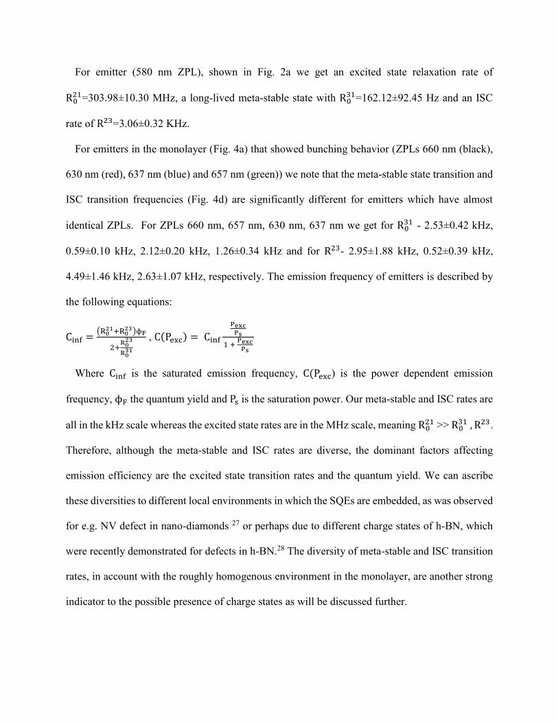
the brightness is significantly different for SQEs which have almost identical ZPLs (in the range
of 89 meV, Fig. 4a). This is surprising due to a more homogenous environment each emitter in the
monolayer should have compared to emitters in multilayers. We therefore firstly analyze the
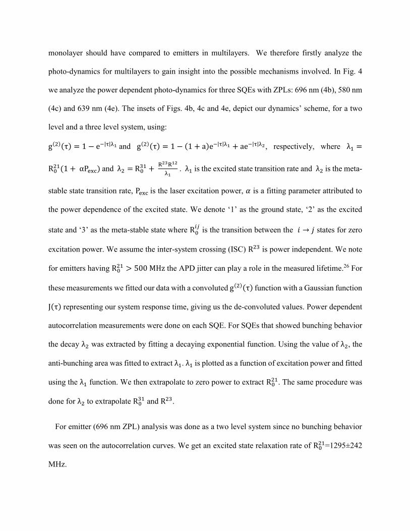
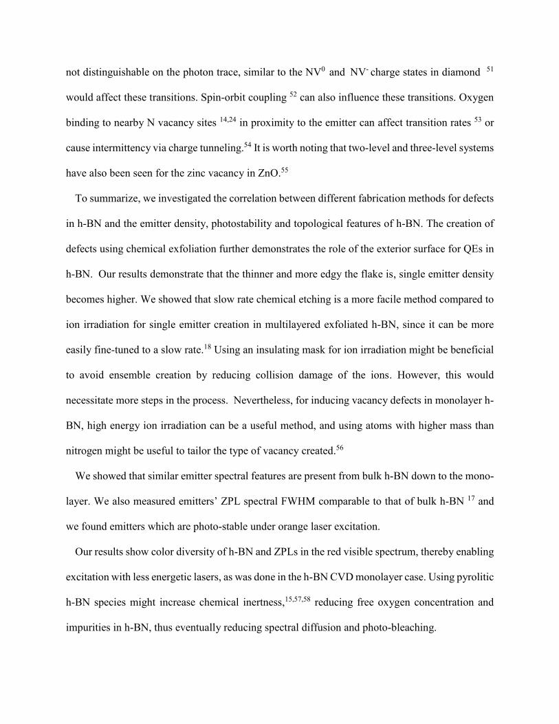
photo-dynamics for multilayers to gain insight into the possible mechanisms involved. In Fig. 4
we analyze the power dependent photo-dynamics for three SQEs with ZPLs: 696 nm (4b), 580 nm
(4c) and 639 nm (4e). The insets of Figs. 4b, 4c and 4e, depict our dynamics’ scheme, for a two
level and a three level system, using:
g(2)(τ) = 1 − e−|τ|λ1 and g(2)(τ) = 1 − (1 + a)e−|τ|λ1 + ae−|τ|λ2, respectively, where λ1 =
R021(1 + αPexc) and λ2 = R0
31 + R23R12
λ1 . λ1 is the excited state transition rate and λ2 is the meta-
stable state transition rate, Pexc is the laser excitation power, 𝛼 is a fitting parameter attributed to
the power dependence of the excited state. We denote ‘1’ as the ground state, ‘2’ as the excited
state and ‘3’ as the meta-stable state where R0𝑖𝑗
is the transition between the 𝑖 → 𝑗 states for zero
excitation power. We assume the inter-system crossing (ISC) R23 is power independent. We note
for emitters having R021 > 500 MHz the APD jitter can play a role in the measured lifetime.26 For
these measurements we fitted our data with a convoluted g(2)(τ) function with a Gaussian function
J(τ) representing our system response time, giving us the de-convoluted values. Power dependent
autocorrelation measurements were done on each SQE. For SQEs that showed bunching behavior
the decay λ2 was extracted by fitting a decaying exponential function. Using the value of λ2, the
anti-bunching area was fitted to extract λ1. λ1 is plotted as a function of excitation power and fitted
using the λ1 function. We then extrapolate to zero power to extract R021. The same procedure was
done for λ2 to extrapolate R031 and R23.
For emitter (696 nm ZPL) analysis was done as a two level system since no bunching behavior
was seen on the autocorrelation curves. We get an excited state relaxation rate of R021=1295±242
MHz.
For emitter (580 nm ZPL), shown in Fig. 2a we get an excited state relaxation rate of
R021=303.98±10.30 MHz, a long-lived meta-stable state with R0
31=162.12±92.45 Hz and an ISC
rate of R23=3.06±0.32 KHz.
For emitters in the monolayer (Fig. 4a) that showed bunching behavior (ZPLs 660 nm (black),
630 nm (red), 637 nm (blue) and 657 nm (green)) we note that the meta-stable state transition and
ISC transition frequencies (Fig. 4d) are significantly different for emitters which have almost
identical ZPLs. For ZPLs 660 nm, 657 nm, 630 nm, 637 nm we get for R031 - 2.53±0.42 kHz,
0.59±0.10 kHz, 2.12±0.20 kHz, 1.26±0.34 kHz and for R23- 2.95±1.88 kHz, 0.52±0.39 kHz,
4.49±1.46 kHz, 2.63±1.07 kHz, respectively. The emission frequency of emitters is described by
the following equations:
Cinf =(R0
21+R023)ϕF
2+R0
23
R031
, C(Pexc) = Cinf
PexcPs
1 + Pexc
Ps
Where Cinf is the saturated emission frequency, C(Pexc) is the power dependent emission
frequency, ϕF the quantum yield and Ps is the saturation power. Our meta-stable and ISC rates are
all in the kHz scale whereas the excited state rates are in the MHz scale, meaning R021 >> R0
31 , R23.
Therefore, although the meta-stable and ISC rates are diverse, the dominant factors affecting
emission efficiency are the excited state transition rates and the quantum yield. We can ascribe
these diversities to different local environments in which the SQEs are embedded, as was observed
for e.g. NV defect in nano-diamonds 27 or perhaps due to different charge states of h-BN, which
were recently demonstrated for defects in h-BN.28 The diversity of meta-stable and ISC transition
rates, in account with the roughly homogenous environment in the monolayer, are another strong
indicator to the possible presence of charge states as will be discussed further.
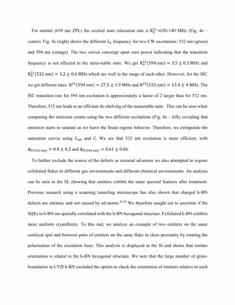
For emitter (639 nm ZPL) the excited state relaxation rate is R021=620±140 MHz (Fig. 4e –
center). Fig. 4e (right) shows the different λ2 frequency for two CW excitations: 532 nm (green)
and 594 nm (orange). The two curves converge upon zero power indicating that the transition
frequency is not affected in the meta-stable state. We get R031(594 nm) = 3.5 ± 0.3 MHz and
R031(532 nm) = 3.2 ± 0.6 MHz which are well in the range of each other. However, for the ISC
we get different rates: R23(594 nm) = 27.5 ± 1.9 MHz and R23(532 nm) = 13.4 ± 4 MHz. The
ISC transition rate for 594 nm excitation is approximately a factor of 2 larger than for 532 nm.
Therefore, 532 nm leads to an efficient de-shelving of the metastable state. This can be seen when
comparing the emission counts using the two different excitations (Fig. 4e – left), revealing that
emission starts to saturate as we leave the linear regime behavior. Therefore, we extrapolate the
saturation curves using Cinf and C. We see that 532 nm excitation is more efficient, with
ϕF(532 nm) = 0.8 ± 0.2 and ϕF(594 nm) = 0.61 ± 0.06.
To further exclude the source of the defects as external ad-atoms we also attempted to expose
exfoliated flakes to different gas environments and different chemical environments. An analysis
can be seen in the SI, showing that emitters exhibit the same spectral features after treatment.
Previous research using a scanning tunneling microscope has also shown that charged h-BN
defects are intrinsic and not caused by ad-atoms.28,29 We therefore sought out to ascertain if the
SQEs in h-BN are spatially correlated with the h-BN hexagonal structure. Exfoliated h-BN exhibits
more uniform crystallinity. To this end, we analyze an example of two emitters on the same
confocal spot and between pairs of emitters on the same flake in close proximity by rotating the
polarization of the excitation laser. This analysis is displayed in the SI and shows that emitter
orientation is related to the h-BN hexagonal structure. We note that the large number of grain-
boundaries in CVD h-BN excluded the option to check the orientation of emitters relative to each
other in CVD h-BN in the same fashion. The spectral features we have observed, where the peak
energy difference fits the splitting between longitudinal (LO) and transverse optical phonons (TO),
is another fingerprint for a defect embedded inside the lattice, as seen also for SQEs in the UV
range.16
We now reflect upon the possible effects of sample preparation methods presented. Carbon
impurities were shown to account for UV luminescence 15 and recently for SQEs in the UV range,
substituting the N vacancy site.16 The chemical treatments and Ar/H2 environments (see SI) the
flakes were exposed to, reduces the probability that organic contaminants are responsible for the
emitters seen, unless a carbon impurity was embedded inside and not exposed to the external areas
of treatment. Since samples were annealed at 850 °C, oxygen should desorb from the flake (above
300 °C 30) as well as gas atoms possibly trapped at interfaces. The suspended h-BN flakes also
discard trapped atoms. We thus conclude that it is unlikely that organic additives or trapped gas
atoms are responsible for the emitters found.
We find that He irradiation generates the highest density of emitters (Table 1). Approximating
the He atom inelastic collision to an electron inelastic collision we can compare to TEM
research.31,32 Temperature variation during irradiation creates different defects shapes 32
demonstrating that defect formation is dependent on the environment around the defect,
emphasizing the importance of using gas during the annealing process compared to vacuum and
could explain the difference in emitter stability. The vacancy sizes created cannot only be point-
like (atomic) but also nano-sized as seen in the TEM images of Refs. 31,32. Annealing at 850 °C
may cause vacancies to diffuse inside the flake 33 similar to diffusion known for the NV defect
annealing in diamond,34 leaving defects not exposed to the external environment. However, for the
mono-layer, the defect is directly exposed to the environment.
Previously, the ZPL of 623 nm was attributed to the anti-site complex (𝑁𝐵𝑉𝑁).17 Our data shows
the ZPL emission line to be between 1.78 eV to 2.18 eV (569 nm to 697 nm), suggesting that other
types of impurities could also be responsible for the observed emission lines. The topological
features we have observed indeed suggest a link between topology and defects. We discuss
possible links comparing TEM data from previous research and density functional calculations.
We note that clear identification of defect structure requires ultra-clean conditions due to the
tendency of adsorbents to substitute defective sites,24,35 possibly also accountable for emission.36
HRTEM has shown interlayer bonding on flake edges (nano-arches),37 which can also be
induced by electron irradiation of h-BN.38 This can explain our observations of emitters located at
perimeters of a flake on top of another flake (Fig. 1d) or at boundaries (Fig. 1c), for untreated
flakes and chemically treated flakes, as shown for the SQE in Fig. 2a. It can also explain our
irradiation results.
The B vacancy (visualized in TEM 39,40,41,42 ) has a high average density of states in the energy
range of 1.78 to 2.18 eV,43 making it a possible candidate. However, the dynamics behind
vacancies in 2D materials can be more complex than in 3D solids: B vacancies exhibit interlayer
bonding behavior seen in bi-layer h-BN which do not occur for the N vacancy 41: N bonds occur
in the layer with the defect and one or two B atoms from the intact layer, reducing the symmetry
of the vacancy from three- to two-fold.40 This type of reconstruction is not observed for mono-
vacancy defects inside multi-layered h-BN which retain their three-fold symmetry.44 This hints at
a connection between the low dimensionality of h-BN to quantum features 45 not seen inside bulk
h-BN but occurring at the boundaries of the material, reminiscent to our observations.
Bonds not native to monocrystalline h-BN may play an important role for visible spectrum
emission. Due to alternating bonds in h-BN (B-N), a non-native bond would be of the type of B-B
or N-N, known as a Homo-elemental bond which belongs in literature to Stone-Wales defects.
These comprise a family of defects which also the 𝑁𝐵𝑉𝑁 complex 17 is included in due to N-N-N
bonds. A Stone-Wales defect can create square-octagon/pentagon–heptagon pairs in h-BN,
changing bond lengths and having charge state configurations. Monolayer h-BN Stone-Wales
defects have been visualized in TEM,46,47 forming due to grain boundaries between domains, thus
decreasing the band-gap and opening new energy states.46 Calculated energy levels suggest
emission in the visible spectral range 48 and with a less dominant phonon DOS of ~ 41 THz (~170
meV), fitting our TO and LO observations.49 We can now link the angular multiplicity we have
seen on perimeters where emitters are clustered (Fig. 1e) as another hint to the presence of Stone-
Wales defects or a grain-boundary effect. 48,49 Grain-boundaries in h-BN have been seen to be up
to 90 µm long,50 well in range of our perimeter lengths. Although N2 ion irradiation has been
shown to generate primarily N vacancy defects, they can also create interstitials which do not
diffuse out of the lattice when annealing at 850 °C. These can create homo-elemental bonds not
native to the lattice,20 and hence also the similarity to monolayer h-BN. Similarly, local changes
in h-BN layer stacking order has been shown via cathodoluminescence to account for a 1 eV range
of emission of excitons (originating at ~200 nm wavelength).13 This raises questions regarding the
value of the band-gap at perimeters in h-BN, which can cause excitation not to be confined inside
the band gap.
The quantum nature of emission and the high transition rates ( > 500 MHz) measured for the
excited states can arise from the reduced dimensionality of h-BN and the small bond lengths ( 1.4
Å 3) which leads to large overlap between orbitals. 45 The variety of meta-stable and ISC transition
frequencies found in CVD monolayer h-BN can have numerous causes. An intermittent charge
state change during the acquisition of photon arrival times in our auto-correlation measurements
not distinguishable on the photon trace, similar to the NV0 and NV- charge states in diamond 51
would affect these transitions. Spin-orbit coupling 52 can also influence these transitions. Oxygen
binding to nearby N vacancy sites 14,24 in proximity to the emitter can affect transition rates 53 or
cause intermittency via charge tunneling.54 It is worth noting that two-level and three-level systems
have also been seen for the zinc vacancy in ZnO.55
To summarize, we investigated the correlation between different fabrication methods for defects
in h-BN and the emitter density, photostability and topological features of h-BN. The creation of
defects using chemical exfoliation further demonstrates the role of the exterior surface for QEs in
h-BN. Our results demonstrate that the thinner and more edgy the flake is, single emitter density
becomes higher. We showed that slow rate chemical etching is a more facile method compared to
ion irradiation for single emitter creation in multilayered exfoliated h-BN, since it can be more
easily fine-tuned to a slow rate.18 Using an insulating mask for ion irradiation might be beneficial
to avoid ensemble creation by reducing collision damage of the ions. However, this would
necessitate more steps in the process. Nevertheless, for inducing vacancy defects in monolayer h-
BN, high energy ion irradiation can be a useful method, and using atoms with higher mass than
nitrogen might be useful to tailor the type of vacancy created.56
We showed that similar emitter spectral features are present from bulk h-BN down to the mono-
layer. We also measured emitters’ ZPL spectral FWHM comparable to that of bulk h-BN 17 and
we found emitters which are photo-stable under orange laser excitation.
Our results show color diversity of h-BN and ZPLs in the red visible spectrum, thereby enabling
excitation with less energetic lasers, as was done in the h-BN CVD monolayer case. Using pyrolitic
h-BN species might increase chemical inertness,15,57,58 reducing free oxygen concentration and
impurities in h-BN, thus eventually reducing spectral diffusion and photo-bleaching.
Further understanding of the origin of SQEs in h-BN can lead to more advanced fabrications
methods in the CVD growth phase or after the growth phase, using ion irradiation and ion
implantation, which has been demonstrated for Si 59, Be 60 and Ar 61 - embedded in the lattice.
Band-gap tuning can be realized using monolayer h-BN as a platform with other monolayer 2D
materials, tailoring the emitter’s energy levels inside the band-gap. Clearly, a wide range of
parameter adjustment can lead to diverse SQE defects in this wide band-gap material.
The work presented here paves the way for deeper understanding of the origin of QEs in h-BN.
It proposes two fabrication methods to create emitters, demonstrating the flexibility of the material
and emphasizing the role topology has on defect dynamics in 2D materials. These results highlight
the diversity in the new arising field of 2D quantum emitters.
Corresponding Author
*Inquiries should be sent to the following e-mail address: [email protected]
Author Contributions
All authors contributed to writing the paper. The authors acknowledge support from the Max
Planck Society as well as the EU via the project DIADEMS and the DFG. AF acknowledges
financial support from the Alexander von Humboldt Foundation. JHS acknowledges financial
support from the EU graphene flagship.
Acknowledgments
The authors thank Sang-Yun Lee, Durga Dasari, Denis Antonov, Marcus Doherty for valuable
discussions, Matthias Widmann for technical support, Andrea Zappe for chemical treatment
assistance and Johannes Greiner for mathematical computational assistance.
REFERENCES:
(1) Kuzuba, T.; Era, K.; Ishii, T.; Sato, T. Solid State Commun. 1978, 25, 863–865.
(2) Serrano, J.; Bosak, a.; Arenal, R.; Krisch, M.; Watanabe, K.; Taniguchi, T.; Kanda, H.;
Rubio, a.; Wirtz, L. Phys. Rev. Lett. 2007, 98 (9), 12–15.
(3) Nagashima, a; Tejima, N.; Gamou, Y.; Kawai, T.; Oshima, C. Phys. Rev. B 1995, 51 (7),
4606–4613.
(4) Alem, N.; Erni, R.; Kisielowski, C.; Rossell, M. D.; Gannett, W.; Zettl, a. Phys. Rev. B -
Condens. Matter Mater. Phys. 2009, 80 (15), 1–7.
(5) Gorbachev, R. V.; Riaz, I.; Nair, R. R.; Jalil, R.; Britnell, L.; Belle, B. D.; Hill, E. W.;
Novoselov, K. S.; Watanabe, K.; Taniguchi, T.; Geim, A. K.; Blake, P. Small 2011, 7 (4),
465–468.
(6) Koperski, M.; Nogajewski, K.; Arora, a.; Cherkez, V.; Mallet, P.; Veuillen, J.-Y.; Marcus,
J.; Kossacki, P.; Potemski, M. Nat. Nanotechnol. 2015, 10 (6), 503–506.
(7) Srivastava, A.; Sidler, M.; Allain, A. V.; Lembke, D. S.; Kis, A.; Imamoğlu, a. Nat.
Nanotechnol. 2015, 10 (6), 491–496.
(8) Upadhyayula, L. C.; Loferski, J. J.; Wold, a.; Giriat, W.; Kershaw, R. J. Appl. Phys. 1968,
39 (10), 4736–4740.
(9) Jelezko, F.; Wrachtrup, J. phys. stat. sol. 2006, 203 (13), 3207–3225.
(10) Museur, L.; Feldbach, E.; Kanaev, A. Phys. Rev. B - Condens. Matter Mater. Phys. 2008,
78 (15), 1–8.
(11) Cassabois, G.; Valvin, P.; Gil, B. Nat. Photonics 2016, 10 (4), 262–266.
(12) Jaffrennou, P.; Barjon, J.; Lauret, J. S.; Attal-Trétout, B.; Ducastelle, F.; Loiseau, a. J. Appl.
Phys. 2007, 102 (11), 44–47.
(13) Bourrellier, R.; Amato, M.; Henrique, L.; Giorgetti, C.; Gloter, A.; Heggie, M. I.; March,
K.; Ste, O.; Reining, L.; Kociak, M. ACS Photonics 2014, No. 1, 857–862.
(14) Museur, L.; Anglos, D.; Petitet, J. P.; Michel, J. P.; Kanaev, A. V. J. Lumin. 2007, 127 (2),
595–600.
(15) Museur, L.; Kanaev, A. J. Mater. Sci. 2009, 44 (10), 2560–2565.
(16) Bourrellier, R.; Meuret, S.; Tararan, A.; Ste, O.; Kociak, M.; Tizei, L. H. G.; Zobelli, A.
Nano Lett. 2016.
(17) Tran, T. T.; Bray, K.; Ford, M. J.; Toth, M.; Aharonovich, I. Nat. Nanotechnol. 2016, 11,
37–41.
(18) Hui, W. C. Proc. SPIE 2004, 5276, 143–153.
(19) Bhimanapati, G. R.; Kozuch, D.; Robinson, J. Nanoscale 2014, 6 (002), 11671–11675.
(20) Jiménez, I.; Jankowski, a. F.; Terminello, L. J.; Sutherland, D. G. J.; Carlisle, J. a.; Doll, G.
L.; Tong, W. M.; Shuh, D. K.; Himpsel, F. J. Phys. Rev. B 1997, 55 (18), 12025–12037.
(21) Kim, K. K.; Hsu, a; Jia, X.; Kim, S. M.; Shi, Y.; Hofmann, M.; Nezich, D.; Rodriguez-
Nieva, J. F.; Dresselhaus, M.; Palacios, T.; Kong, J. Nano Lett. 2011, xx, xx.
(22) Wse, B.; Kumar, S.; Kaczmarczyk, A.; Gerardot, B. D. Nano Lett. 2015, 15, 7567–7573.
(23) Oba, F. Phys. Rev. B 2010, 81, 075125,1–6.
(24) Krivanek, O. L.; Chisholm, M. F.; Nicolosi, V.; Pennycook, T. J.; Corbin, G. J.; Dellby, N.;
Murfitt, M. F.; Own, C. S.; Szilagyi, Z. S.; Oxley, M. P.; Pantelides, S. T.; Pennycook, S. J.
Nature 2010, 464 (7288), 571–574.
(25) Tonndorf, P.; Schmidt, R.; Schneider, R.; Kern, J.; Buscema, M.; Steele, G. a.; Castellanos-
Gomez, A.; van der Zant, H. S. J.; Michaelis de Vasconcellos, S.; Bratschitsch, R. Optica
2015, 2 (4), 347.
(26) Wang, C.; Kurtsiefer, C.; Weinfurter, H.; Burchard, B. J. Phys. B At. Mol. Opt. Phys. 2006,
39 (1), 37.
(27) Inam, F. a.; Gaebel, T.; Bradac, C.; Stewart, L.; Withford, M. J.; Dawes, J. M.; Rabeau, J.
R.; Steel, M. J. New J. Phys. 2011, 13.
(28) Wong, D.; Velasco, J.; Ju, L.; Lee, J.; Kahn, S.; Tsai, H.-Z.; Germany, C.; Taniguchi, T.;
Watanabe, K.; Zettl, A.; Wang, F.; Crommie, M. F. Nat. Nanotechnol. 2015, 10 (11), 949–
953.
(29) Chandni, U.; Watanabe, K.; Taniguchi, T.; Eisenstein, J. P. Nano Lett. 2015, 15 (11), 7329–
7333.
(30) Nurunnabi, M.; Nafiujjaman, M.; Lee, S.-J.; Park, I.-K.; Huh, K. M.; Lee, Y. Chem.
Commun. 2016, 52, 6146–6149.
(31) Kotakoski, J.; Jin, C. H.; Lehtinen, O.; Suenaga, K.; Krasheninnikov, a. V. Phys. Rev. B -
Condens. Matter Mater. Phys. 2010, 82 (11), 1–4.
(32) Cretu, O.; Lin, Y.-C.; Suenaga, K. Micron 2015, 72, 21–27.
(33) Zobelli, a.; Ewels, C. P.; Gloter, a.; Seifert, G. Phys. Rev. B - Condens. Matter Mater. Phys.
2007, 75 (9), 1–7.
(34) Fávaro de Oliveira, F.; Momenzadeh, S. A.; Antonov, D.; Scharpf, J.; Osterkamp, C.;
Naydenov, B.; Jelezko, F.; Denisenko, A.; Wrachtrup, J. Nano Lett. 2016,
acs.nanolett.5b04511.
(35) Wei, X.; Wang, M.; Bando, Y.; Golberg, D. ACS Nano 2011, 5 (4), 2916–2922.
(36) Park, H.; Wadehra, A.; Wilkins, J. W.; Neto, A. H. C.; Park, H.; Wadehra, A.; Wilkins, J.
W.; Neto, A. H. C. Appl. Phys. Lett. 2012, 100 (253115), 1–5.
(37) Nistor, L.; Teodorescu, V.; Ghica, C.; Landuyt, J. Van; Dinca, G. Diam. Relat. Mater. 2001,
10, 1352–1356.
(38) Bengu, E.; Leslie, C.; Marks, L. D.; Bengu, E.; Leslie, C.; Marks, L. D. 1998, 72 (3), 314–
315.
(39) Cheng, G.; Yao, S.; Sang, X.; Hao, B.; Zhang, D.; Yap, Y. K.; Zhu, Y. Small 2016, 12 (6),
818–824.
(40) Rasool, H. I.; Ophus, C.; Zettl, A. Adv. Mater. 2015, 27 (38), 5771–5777.
(41) Alem, N.; Yazyev, O. V.; Kisielowski, C.; Denes, P.; Dahmen, U.; Hartel, P.; Haider, M.;
Bischoff, M.; Jiang, B.; Louie, S. G.; Zettl, a. Phys. Rev. Lett. 2011, 106 (12), 1–4.
(42) Jin, C.; Lin, F.; Suenaga, K.; Iijima, S. Phys. Rev. Lett. 2009, 102 (19), 3–6.
(43) Okada, S. Phys. Rev. B - Condens. Matter Mater. Phys. 2009, 80 (16), 1–4.
(44) Meyer, J. C.; Chuvilin, A.; Algara-Siller, G.; Biskupek, J.; Kaiser, U. Nano Lett. 2009, 9
(7), 2683–2689.
(45) Huang, B.; Cao, X. K.; Jiang, H. X.; Lin, J. Y.; Wei, S. Phys. Rev. B 2012, 155202 (86), 1–
5.
(46) Li, Q.; Zou, X.; Liu, M.; Sun, J.; Gao, Y.; Qi, Y.; Zhou, X.; Yakobson, B. I.; Zhang, Y.;
Liu, Z. Nano Lett. 2015, 15 (9), 5804–5810.
(47) Cretu, O.; Lin, Y.; Suenaga, K. Nano Lett. 2014, 14, 1064–1068.
(48) Liu, Y.; Zou, X.; Yakobson, B. I. ACS Nano 2012, 6 (8), 7053–7058.
(49) Wang, R.; Yang, J.; Wang, S. Nanoscale 2016, 8, 8210–8219.
(50) Lu, G.; Wu, T.; Yuan, Q.; Wang, H.; Wang, H.; Ding, F.; Xie, X.; Jiang, M. Nat. Commun.
2015, 6, 1–7.
(51) Aslam, N.; Waldherr, G.; Neumann, P.; Jelezko, F.; Wrachtrup, J. New J. Phys. 2015,
013064 (15), 1–17.
(52) Goldman, M. L.; Sipahigil, A.; Doherty, M. W.; Yao, N. Y.; Bennett, S. D.; Markham, M.;
Twitchen, D. J.; Manson, N. B.; Kubanek, A.; Lukin, M. D. Phys. Rev. Lett. 2015, 145502
(114), 1–6.
(53) Tews, K. H. J. Lumin. 1974, 9, 223–239.
(54) Bradac, C.; Gaebel, T.; Pakes, C. I.; Say, J. M.; Zvyagin, A. V; Rabeau, J. R. 2013, No. 1,
132–139.
(55) Morfa, A. J.; Gibson, B. C.; Karg, M.; Karle, T. J.; Greentree, A. D.; Mulvaney, P.;
Tomljenovic-hanic, S. 2012.
(56) Lehtinen, O.; Dumur, E.; Kotakoski, J.; Krasheninnikov, a. V.; Nordlund, K.; Keinonen, J.
Nucl. Instruments Methods Phys. Res. Sect. B Beam Interact. with Mater. Atoms 2011, 269
(11), 1327–1331.
(57) Moore, a. J. Cryst. Growth. 1990, pp 6–15.
(58) Le Gallet, S.; Chollon, G.; Rebillat, F.; Guette, a.; Bourrat, X.; Naslain, R.; Couzi, M.;
Bruneel, J. L. J. Eur. Ceram. Soc. 2004, 24 (1), 33–44.
(59) He, B.; Qiu, M.; Yuen, M. F.; Zhang, W. J. Appl. Phys. Lett. 2014, 105, 0121041(1–4).
(60) He, B.; Zhang, W. J.; Yao, Z. Q.; Chong, Y. M.; Yang, Y.; Ye, Q.; Pan, X. J.; Zapien, J. A.;
Bello, I.; Lee, S. T.; Zutz, H.; Hofsäss, H.; He, B.; Zhang, W. J.; Yao, Z. Q.; Chong, Y. M.;
Yang, Y.; Ye, Q.; Pan, X. J. Appl. Phys. Lett. 2009, 95 (2009), 252106(1–3).
(61) Cun, H.; Iannuzzi, M.; Hemmi, A.; Roth, S.; Osterwalder, J.; Greber, T. Nano Lett. 2013,
13, 2098–2103.
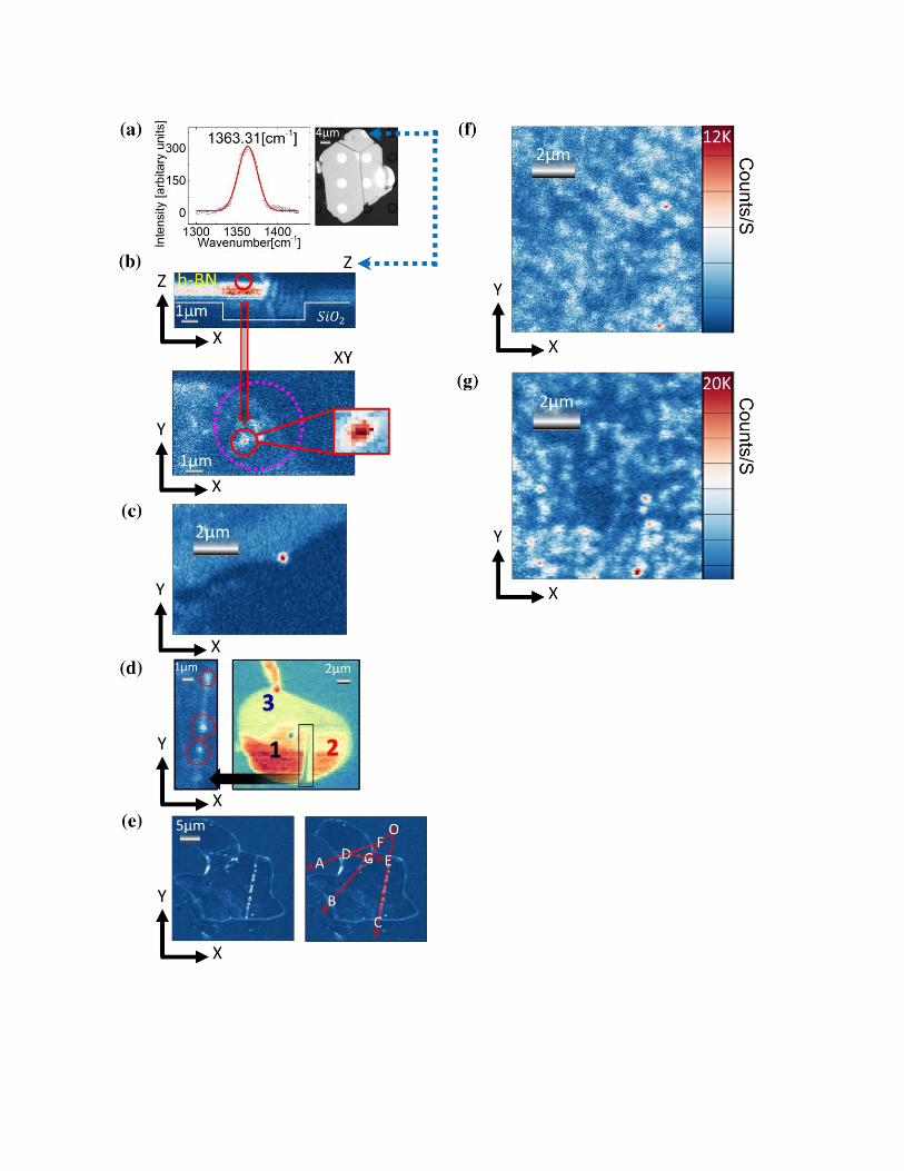
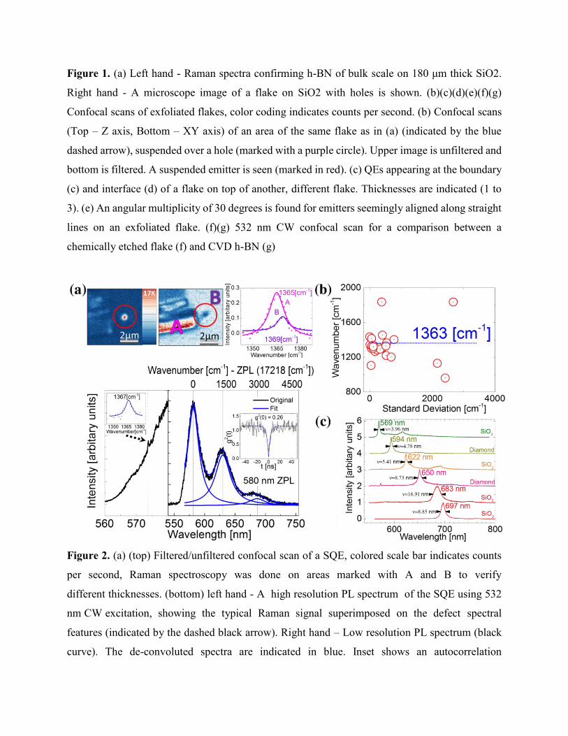
Figure 1. (a) Left hand - Raman spectra confirming h-BN of bulk scale on 180 μm thick SiO2.
Right hand - A microscope image of a flake on SiO2 with holes is shown. (b)(c)(d)(e)(f)(g)
Confocal scans of exfoliated flakes, color coding indicates counts per second. (b) Confocal scans
(Top – Z axis, Bottom – XY axis) of an area of the same flake as in (a) (indicated by the blue
dashed arrow), suspended over a hole (marked with a purple circle). Upper image is unfiltered and
bottom is filtered. A suspended emitter is seen (marked in red). (c) QEs appearing at the boundary
(c) and interface (d) of a flake on top of another, different flake. Thicknesses are indicated (1 to
3). (e) An angular multiplicity of 30 degrees is found for emitters seemingly aligned along straight
lines on an exfoliated flake. (f)(g) 532 nm CW confocal scan for a comparison between a
chemically etched flake (f) and CVD h-BN (g)
Figure 2. (a) (top) Filtered/unfiltered confocal scan of a SQE, colored scale bar indicates counts
per second, Raman spectroscopy was done on areas marked with A and B to verify
different thicknesses. (bottom) left hand - A high resolution PL spectrum of the SQE using 532
nm CW excitation, showing the typical Raman signal superimposed on the defect spectral
features (indicated by the dashed black arrow). Right hand – Low resolution PL spectrum (black
curve). The de-convoluted spectra are indicated in blue. Inset shows an autocorrelation
measurement of the SQE. (b) Conversion of 23 emitter PL spectrum acquired from various sources
from treated/untreated flakes to the difference in wavenumber between adjacent peaks as a
function of standard deviation. (c) PL spectrum using 532 nm CW excitation from h-BN on
different substrates (indicated for each curve). ν denotes the ZPL full width half maximum in nm.
Figure 3. CVD mono-layer PL spectra using 532 nm CW excitation (a) (left) PL spectra for 3
emitters (right) PL spectra for a suspended emitter. (b) 594 nm CW excitation using a 600LP filter
(left). Emission count from an emitter with a 640 nm ZPL for 45 min (right) PL spectra for 4
emitters.
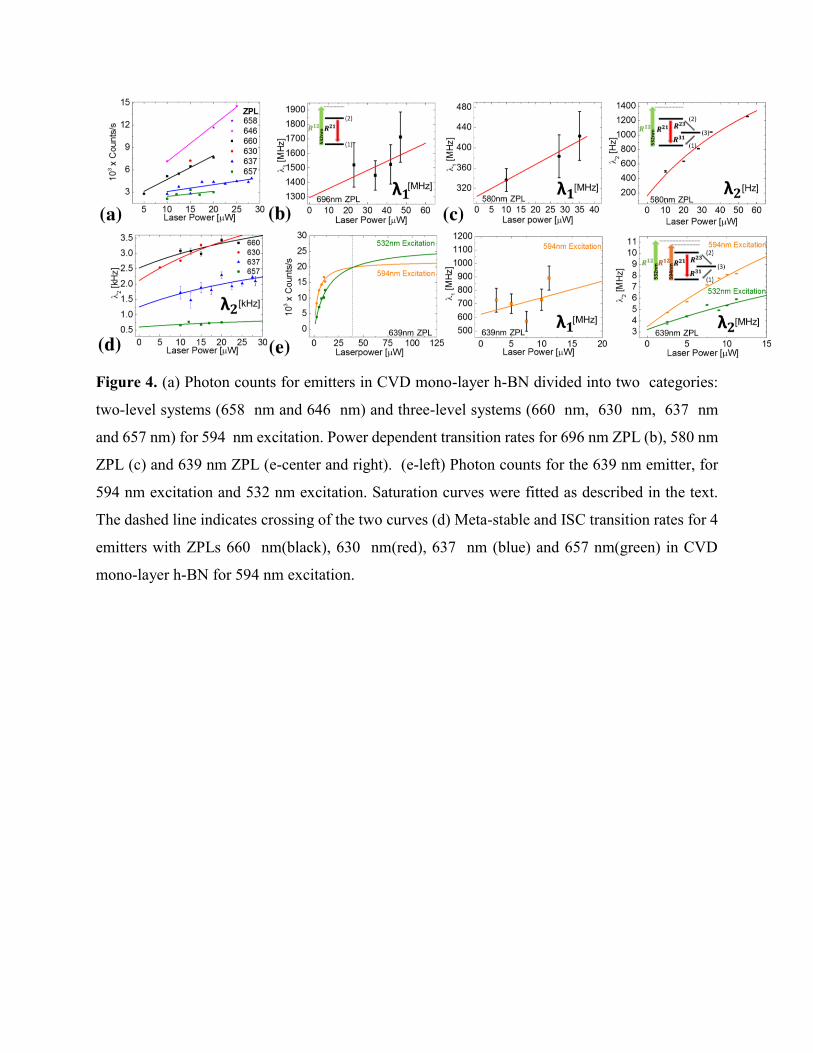
Figure 4. (a) Photon counts for emitters in CVD mono-layer h-BN divided into two categories:
two-level systems (658 nm and 646 nm) and three-level systems (660 nm, 630 nm, 637 nm
and 657 nm) for 594 nm excitation. Power dependent transition rates for 696 nm ZPL (b), 580 nm
ZPL (c) and 639 nm ZPL (e-center and right). (e-left) Photon counts for the 639 nm emitter, for
594 nm excitation and 532 nm excitation. Saturation curves were fitted as described in the text.
The dashed line indicates crossing of the two curves (d) Meta-stable and ISC transition rates for 4
emitters with ZPLs 660 nm(black), 630 nm(red), 637 nm (blue) and 657 nm(green) in CVD
mono-layer h-BN for 594 nm excitation.