Embed Size (px)
Citation preview
Wasserstoffeffekt und -analyse in der GDS -
Anwendungen in der Werkstoffforschung
(Hydrogen Effect and Analysis in GDS –
Applications in Material Science)
Der Fakultät Maschinenwesen
der
Technischen Universität Dresden
zur
Erlangung des akademischen Grades
Doktoringenieur (Dr.-Ing.)
vorgelegte Dissertation
Diplom-Physiker Hodoroaba, Vasile-Dan
geb. am 28.02.1969 in Bacau, Rumänien
Tag der Einreichung: 30.04.2002
Danksagungen/Acknowledgements
Die vorliegende Arbeit entstand in der Zeit vom Mai 1998 bis März 2002 in der Bundesanstalt für Materialforschung und -prüfung (BAM), Berlin, im Institut für Festkörperanalytik und Strukturforschung des Instituts für Festkörper- und Werkstoffforschung IFW Dresden e. V. und im Institut für Spektrochemie und Angewandte Spektroskopie (ISAS), Dortmund.
Herrn Prof. M. Hennecke, Herrn Prof. W. Paatsch, Herrn Prof. G. Reiners und Herrn Dr. W. Unger danke ich für die Ermöglichung und Förderung dieser Arbeit im Rahmen des BAM-Doktorandenprogramms und für die harmonische Zusammenarbeit unter Bedingungen, von denen ich sehr profitiert habe.
Herrn Prof. K. Wetzig danke ich für die Betreuung dieser Arbeit, für seine ständige Unterstützung und zahlreiche interessante Diskussionen.
Herrn Dr. V. Hoffmann und seinen Mitarbeitern - Dr. R. Dorka, Dipl.-Phys. L. Wilken, Dipl.-Ing. G. Pietzsch, Dipl.-Chem. M. Kunstár - (IFW Dresden) danke ich für die exzellente Zusammenarbeit. Der großen Erfahrung von Dr. Hoffmann im GDS Bereich bin ich sehr dankbar.
Many thanks to Prof. E.B.M. Steers (University of North London) for his decisive contribution to the understanding of the complex effect of hydrogen, for his numerous visits and thorough and helpful discussions. Funding from EU-GDS Network for visits and meetings is gratefully acknowledged, too.
Herrn Dipl.-Phys. Th. Wirth, Herrn Dr. M. Procop, Herrn Dipl.-Ing. D. Schmidt und Frau Dr. I. Retzko (BAM, Berlin) danke ich herzlich für ihre permanente Hilfe in den unterschiedlichsten Bereichen im und außerhalb des Labors.
Herrn Dr. H. Jenett (ISAS, Dortmund) danke ich für seine langjährige Kooperation, Freundlichkeit und nicht zuletzt für seine Unterstützung beim Übergang vom SNMS- zum GD-OES Gebiet.
Berlin, 30. April 2002
3
Contents
SYMBOLS USED.........................................................................................................................................................5
1 INTRODUCTION ............................................................................................................................................6
2 PRE-CONSIDERATIONS.............................................................................................................................11
2.1 PHYSICAL FUNDAMENTALS OF GDS............................................................................................................... 11
2.1.1 GD-OES................................................................................................................................................ 15
2.1.1.1 DC-GD-OES QUANTIFICATION.......................................................................................................16
2.1.1.2 RF-GD............................................................................................................................................18
2.1.2 GD-MS.................................................................................................................................................. 20
2.2 STATE-OF-THE-ART OF THE ANALYSIS OF LIGHT ELEMENTS (H, C, N, O) (I) AS CONTAMINATION AND (II) AS A
SAMPLE CONSTITUENT .................................................................................................................................... 21
2.3 ALTERNATIVE METHODS SELECTED FOR DEPTH PROFILING OF THIN LAYERS CONTAINING LIGHT ELEMENTS
(SNMS, SIMS, NRA) .................................................................................................................................... 25
3 OBJECTIVES.................................................................................................................................................27
4 EXPERIMENTAL..........................................................................................................................................29
4.1 GD-OES......................................................................................................................................................... 29
4.2 GD-MS ......................................................................................................................................................... 33
4.3 HYDROGEN/CARRIER GAS MIXING SYSTEM ..................................................................................................... 34
4.4 HFM PLASMA SNMS..................................................................................................................................... 36
4.5 TOF-SIMS...................................................................................................................................................... 38
4.6 NRA............................................................................................................................................................... 38
5 FUNDAMENTAL INVESTIGATIONS .......................................................................................................40
5.1 EFFECT OF HYDROGEN IN GDS ....................................................................................................................40
5.1.1 EFFECT OF HYDROGEN IN AN ARGON GD WHEN COPPER IS THE SAMPLE ................................................ 40
5.1.1.1 ATOMIC (CU I) AND IONIC (CU II) LINES OF COPPER ..................................................................... 41
5.1.1.2 ATOMIC (AR I) AND IONIC (AR II) LINES OF ARGON ...................................................................... 45
5.1.1.3 HYDROGEN (LINE, BAND AND CONTINUUM) SPECTRUM ................................................................ 49
5.1.1.4 DISCUSSION................................................................................................................................... 50
5.1.2 EFFECT OF HYDROGEN IN A NEON GD WHEN COPPER IS THE SAMPLE..................................................... 54
5.1.2.1 EMISSION LINES OF COPPER (CU I AND CU II), NEON (NE I AND NE II) AND HYDROGEN ............... 54
5.1.2.2 DISCUSSION AND COMPARISON WITH THE ARGON CASE................................................................. 56
5.1.3 HYDROGEN CONTINUUM ........................................................................................................................ 57
5.1.3.1 EXPERIMENTAL INVESTIGATIONS .................................................................................................. 57
5.1.3.2 THEORY AND DISCUSSION ............................................................................................................. 60
5.1.4 ADDITIONAL INVESTIGATIONS OF THE HYDROGEN EFFECT BY GD-MS ................................................. 62
4
5.1.5 EFFECT OF HYDROGEN ON LINE INTENSITIES FROM VARIOUS ANALYTES IN COMMON BULK MATERIALS
(COPPER, LOW ALLOY STEEL, ALUMINIUM, TITANIUM AND SILICON WAFERS)......................................... 64
5.1.5.1 EFFECT OF HYDROGEN ON LINE INTENSITIES OF VARIOUS ANALYTES WHEN ARGON IS THE CARRIER
GAS............................................................................................................................................................ 64
5.1.5.2 EFFECT OF HYDROGEN ON LINE INTENSITIES OF VARIOUS ANALYTES WHEN NEON IS THE CARRIER
GAS............................................................................................................................................................ 66
5.1.5.3 DISCUSSION................................................................................................................................... 66
5.1.6 MOLECULAR BANDS OF COMPOUNDS CONTAINING HYDROGEN.............................................................. 70
5.1.7 EFFECT OF HYDROGEN ON THE SPUTTERING RATE AND SPUTTERING CRATER SHAPE.............................. 72
5.1.8 COMPARATIVE USE OF DIFFERENT HYDROGEN SOURCES (I) AS A GASEOUS IMPURITY AND (II) AS A
SAMPLE CONSTITUENT (TIH2) ................................................................................................................. 76
5.1.9 INFLUENCE OF THE GD PARAMETERS ON THE HYDROGEN EFFECT ......................................................... 81
5.1.9.1 USE OF DIFFERENT OPERATING MODES .......................................................................................... 81
5.1.9.2 USE OF VARIOUS GD PARAMETERS ............................................................................................... 82
5.2 DEPTH PROFILING OF THIN MULTILAYER COATINGS. OPTIMISATION OF THE DEPTH RESOLUTION..........84
5.2.1 GD-OES PROCEDURE FOR THE OPTIMISATION OF THE DEPTH RESOLUTION............................................ 84
5.2.2 HFM PLASMA SNMS PROCEDURE FOR THE OPTIMISATION OF THE DEPTH RESOLUTION ........................ 86
6 APPLICATIONS IN MATERIAL SCIENCE .............................................................................................89
6.1 IMPROVEMENT OF SENSITIVITY AND DETECTION LIMIT IN GD-OES BY HYDROGEN ADDITION ....................... 89
6.2 EXPLOITATION OF THE HYDROGEN EFFECT ON GD-OES THIN FILM ANALYSIS ............................................... 92
6.2.1 POSSIBILITIES AND LIMITATIONS OF GD-OES DEPTH PROFILING OF THIN MULTILAYER MATERIALS. SELECTIVE COMPARISON WITH HFM PLASMA SNMS AND TOF-SIMS........................................................... 92
6.2.2 IMPROVEMENT OF THE GD-OES DEPTH RESOLUTION BY HYDROGEN ADDITION .................................... 96
6.2.3 INFLUENCE OF THE GD SOURCE CONTAMINATION ON THE GD-OES ANALYSIS OF VERY THIN LAYERS . 98
6.2.4 EVALUATION OF THE ATTAINED DEPTH RESOLUTION ........................................................................... 100
6.3 GD-OES ANALYSIS OF HYDROGEN IN ELECTROPLATED SYSTEMS. ............................................................... 102
6.3.1 GD-OES ANALYSIS OF HYDROGEN IN VARIOUS ELECTROPLATED COATINGS (COPTW, CR, CD) ......... 102
6.3.2 GD-OES ANALYSIS OF ELECTROLYTICALLY COATED ZINC ON STEEL. COMPARISON WITH HOT DIP ZINC
COATING ....................................................................................................................................................... 107
7 CONCLUSIONS...........................................................................................................................................114
8 REFERENCES .............................................................................................................................................117
Symbols used 5
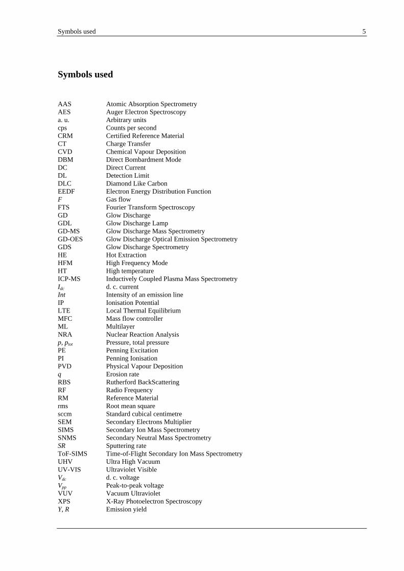
Symbols used
AAS Atomic Absorption Spectrometry AES Auger Electron Spectroscopy a. u. Arbitrary units cps Counts per second CRM Certified Reference Material CT Charge Transfer CVD Chemical Vapour Deposition DBM Direct Bombardment Mode DC Direct Current DL Detection Limit DLC Diamond Like Carbon EEDF Electron Energy Distribution Function F Gas flow FTS Fourier Transform Spectroscopy GD Glow Discharge GDL Glow Discharge Lamp GD-MS Glow Discharge Mass Spectrometry GD-OES Glow Discharge Optical Emission Spectrometry GDS Glow Discharge Spectrometry HE Hot Extraction HFM High Frequency Mode HT High temperature ICP-MS Inductively Coupled Plasma Mass Spectrometry Idc d. c. current Int Intensity of an emission line IP Ionisation Potential LTE Local Thermal Equilibrium MFC Mass flow controller ML Multilayer NRA Nuclear Reaction Analysis p, ptot Pressure, total pressure PE Penning Excitation PI Penning Ionisation PVD Physical Vapour Deposition q Erosion rate RBS Rutherford BackScattering RF Radio Frequency RM Reference Material rms Root mean square sccm Standard cubical centimetre SEM Secondary Electrons Multiplier SIMS Secondary Ion Mass Spectrometry SNMS Secondary Neutral Mass Spectrometry SR Sputtering rate ToF-SIMS Time-of-Flight Secondary Ion Mass Spectrometry UHV Ultra High Vacuum UV-VIS Ultraviolet Visible Vdc d. c. voltage Vpp Peak-to-peak voltage VUV Vacuum Ultraviolet XPS X-Ray Photoelectron Spectroscopy Y, R Emission yield
1 Introduction 6
1 Introduction
The development and production of new materials is nowadays only possible by high material and technical costs. With respect to the material science, this means a rapid, new and further development of various analytical procedures. On the other hand, high quality materials can be produced only by complicate technologies, the control of their parameters being a prerequisite of a good quality of the final product. In order to clarify the causes of failures in the quality of a new material subtle investigation methods are necessary to be implemented in practice. Therefore, material science can be applied (i) in research and development as well as (ii) in the quality control and failure analysis.
Inherently in material science, the material properties are necessary to be improved. Basic problematic such as corrosion resistance or wear resistance are markedly solved by coating technologies. For example, electroplated steel sheets with zinc based coatings, widely used in the automotive and home appliance industries, are characterised by good corrosion resistance. Moreover, superior properties in welding and painting are achieved by plating the steel sheets with a thick layer of several µm. Physical Vapour Deposition (PVD) and Chemical Vapour Deposition (CVD) coatings, such as nitrides, carbides or carbonitrides, etc, are commonly used in order to increase the wear resistance of cutting tools or gear wheels. Hard coatings are also used to create decorative finishes for consumer goods.
High-temperature (HT) applications, e.g., heat-transfer systems for energy conversion, gas turbines for power generation and for chemical process heat utilisation, need metallic materials, such as nickel and iron based alloys, which must be able to combine high stress rupture strength, good fatigue strength and good resistance against the attack of oxygen-, carbon- and/or sulphur containing atmospheres at working temperatures higher as 600 C. Added to the bulk material in order to improve its behaviours at such elevated temperatures, Cr, Al or Y2O3, are responsible for the formation of protective dense oxide scales, whose chemical composition and in-depth distribution are decisive for the lifetime of the material.
Many of the materials necessary to be investigated are electrically conductive and therefore often possible to be analysed accurately by a low cost method. With a continuous increasing impact in the fields of most various types of applications, electrically non-conductive samples (bulk or coatings) are challenging more and more the analytical methods. Oxides such as SiO2, and Al2O3, almost always present as main compounds in bulk glasses and ceramics, but also coating layers such as SiO2, TiO2, SnO2, etc, are just an example very often used in practice - as, e.g., isolation layers or optical coatings. Their investigation by, e.g., wet chemistry is very costly. The direct solid sampling must be implemented in this case. This might avoid the intermediary technique of pressing the non-conductive powder of the solid material to be analysed together with a conductive host matrix in a solid pellet. Having additionally a low thermal conductivity, too, organic coatings, polymers or lacquers are possible to be analysed only in restricted conditions by only a few methods.
Mostly dealing with thin layer (<100 nm) technologies, the microelectronic industry is permanent interested in analytical methods able to characterise the more and more miniaturised electronic devices. Generally they contain combinations of thin layers with special electric and magnetic properties, semiconductors and/or barrier diffusion interlayers.
1 Introduction 7
Structures in the range of only a few nm are crucial for the macroscopic properties of the material in this particular application field.
As the relevant material properties are decisively determined by the elemental composition, it is clear that a quantitative elemental analysis is absolutely necessary in order to get the ultimate performance, efficiency, stability and yield of the resulting material. It would be ideally to have to disposal non-destructive analytical methods able to inspect the material with maximum accuracy from its top surface down to the depth of interest, often hundreds of µm. The analytical methods are demanded to supply very low detection limits for trace elements, however, high accuracy being sometimes simultaneously necessary for the major and minor constituents, too. Analysis of nanostructures is possible only by using techniques characterised by a high lateral resolutions. Even when such analytical figures of merit are excellent, it can be possible that the applied analytical techniques are expensive, time consuming or make necessary complicate sample preparations. Such aspects are not to be ignored at all in the routine industrial applications. These are only some of the common problems to deal with in technological applications. The correct decision and planning, which analytical method might be applied in order to get the best knowledge, is the result of the rapid transfer from basic research and development in material/surface science.
There are more than 50 modern analytical methods which have been developed in the recent decades for the investigation of the material in bulk or at its surface. All these methods are in principle based on the interaction taking place, when energy from well characterised bombarding particles (primary electrons, ions, neutrals or photons) is transmitted to the solid to be investigated. The "response" of the solid, in turn in form of secondary emitted electrons, ions, neutrals or photons is analysed and hence the elemental/chemical concentration and its distribution in the solid can be deduced. From this large variety of spectroscopies, each of them having advantages and disadvantages, but acting complementarily, the optimal technique must be chosen depending on the individual analytical application. Non-destructive techniques are mainly used in surface or thin film analysis, due to the excitation (only) of the particles localised in the solid in the near surface region by an electron, photon or ion beam, respectively [Auger Electron Spectroscopy (AES), X-Ray Photoelectron Spectroscopy (XPS), Rutherford BackScattering (RBS), etc].
As the interest in the present work is expanded to material depth in the µm range, destructive techniques have been applied successfully. Using the ion bombardment for the removal of the sample material, Secondary Ion Mass Spectrometry (SIMS) should be considered the most appropriate technique for depth profile analysis. However, the number and the character of the secondary ions emitted in the sputter process are strongly dependent on the matrix. Bombarding ions can be efficiently used for sputtering and supplying the analytical signal if an electrical field accelerates the ions to the biased sample surface, as in spark and arc spectroscopy. Superior to them, gas discharges or low pressure plasmas are not only responsible for supplying the primary ions, but also the excitation or ionisation of the sputtered particles take place independent of the matrix in a separate medium. This is the case of Glow Discharge (GD) spectroscopy and plasma SNMS (Secondary Neutral Mass Spectrometry), both used in this work, due to their similarities. Note that GD Spectroscopy (GDS) may refer to optical emission (GD-OES) or absorption (GD-AAS) as well as to mass spectrometry (GD-MS).
On the other hand, the combination of controlled removal of sample particles by an ion beam or the cross-sectioning of the layered sample and the subsequently application of electron or
1 Introduction 8
photon spectroscopies offers often the solution to various analytical problems, e.g., depth profiling of thick coatings. Such hybrid instruments are nowadays largely offered by the manufacturing companies. However, despite of the excellent figures of merit, they are expensive, have high operational costs, and the sample throughput is low.
Mostly used in the present work, GD-OES is a technique which has already gained its place in the analysis of electrically conductive bulk materials (especially in its incipient phase) as well as in depth profiling of thick and thin coatings. One can distinguish the two GD excitation modes:
DC-GD, when a continuous voltage is applied on the sample and the GD is controlled by three macroscopic parameters, voltage, current and pressure, and RF-GD, when at the backside of the sample a rf-voltage is applied. It should be also noted that the type of GD source used in this work is a so-called GRIMM type and the rf-powering mode was operated in the free-running system, as it was recently (1995) developed by HOFFMANN et al. in IFW DRESDEN.[1] There are also other configurations, e.g., MARCUS GD source (not used in this work).
Due to the very high rates of cathodic sputtering (10 200 nm/s) accompanied by a large dynamic range of detection limits of 1 100 µg/g for almost all the elements of the periodic table, GD-OES is very popular in the steel and automotive industries. Based on a multimatrix quantification algorithm developed recently,[2] optical intensity vs. sputtering time profiles can be easily converted into elemental concentration vs. sputtered depth (i.e., quantitative profiles). This empirical quantification procedure is established as working reliable. It takes into account, among others, the dependence of the measured intensities on the GD parameters which control the GD operation. However, this is not the case for non-conductive samples, the RF-GD being controlled by more complicate parameters. The correct measurement of the rf parameters makes object of investigations which are in a continuing progress. Nevertheless, qualitatively, RF-GD-OES depth profiling often supplies quick results, which are welcome as first analytical results. E.g., it responds to questions such as what elements are present in the sample, how many layers are in the coating or if an element is present at an interface, good-bad comparison, and so on.
As the sample to be GD-OES investigated plays the role of the cathode of the GD source, it must fulfil some conditions. The sample must be a solid having a flat surface (although wires or other regular shapes can be in particular mountings also analysed) with a diameter of at least 10 mm. The GD working at low pressures, i.e., several hundreds of Pa, the sample, as part of the GD source, must be vacuum tight. Special attention is paid to this point, the influence of external gas contamination being necessary to be avoided. High roughness of the sample surface or a leak are able to cause unlike effects in the operation of the analytical GD. This aspect will be extensively investigated in this work. As far as the sample thickness is concerned, due to its electrical capacity, a non-conductive sample can barely be rf-sputtered at 4-5 mm thickness, e.g., glasses or ceramics. One big advantage of GDS is the high depth range which it is able to be inspected. The special configuration of the GD source makes possible sample sputtering layer by layer up to more than 100 µm. Nevertheless, it was also recently reported [3-6] that layers of only few nm thickness were accurately GD-OES depth profiled. Depending on the diameter of the anode used, a relatively big sputtering crater of 8 down to 1 mm is obtained. This means that in this range of analysable area the sample must be laterally homogeneous, in terms of both elemental concentration and depth distribution. Lower diameters are desired by some applications from industry, however a markedly
1 Introduction 9
diminishing of the analytical signal makes a further miniaturising of the GD source rather impossible.
Depth profiling of non-conductive thin coatings is no simple analytical task. With increasing success RF-GD-OES is trying to supply a routine analytical method for depth profiling of such samples. Part of this work was devoted to this subject. In order to establish the capabilities, but also the deficiencies of the implementation of RF-GD-OES as a routine procedure for depth profiling of non-conductive samples, HFM (High Frequency Mode) plasma SNMS was comparatively tested for some relevant examples of materials. Plasma SNMS may be considered as the only analytical technique similar to GDS as far as the basic processes are involved, namely (i) bombarding of the solid sample to be analysed by noble gas ions produced by a plasma, (ii) sputtering and (iii) subsequent separate delivering of the analytical signal (however by ionisation, not by excitation as in GD-OES). Layer stacks such as SiO2/TiO2 or Si3N4/SiO2 (100 nm single layer thickness) have been deposited by PVD and CVD on various substrates in the frame of a VAMAS project in BAM and SCHOTT
GLASSWERKE (Mainz, Germany) as multilayer reference coatings. Layered certified reference materials (CRM) are needed as check standards for ensuring depth profiling accuracy and comparability between individual users. For example, it is very often necessary to determine the thickness of a SiO2 layer. Sputtering SiO2 layers with various certified thickness at fixed GD parameters might supply immediately the unknown thickness by a simple conversion of the sputtering times into the thickness.
However, as a prerequisite, laborious optimisation procedures are necessary to be carried out for both methods, especially for non-conductive materials, in order to obtain that depth profile characterised by the best depth resolution. Such procedures are detailed described in Sec. 5.2. They are useful, because one can avoid unnecessary corrections with respect to the substantial dependence on the rf parameters at the RF-GD-OES quantification. Specific analytical problems, such as the in-depth distribution of alkali metals in coated BK7 glass are also comparatively investigated.
The most part of the present work was devoted to investigations of a very complex effect, caused by the presence of hydrogen even in very small amounts, i.e., <0.1% v/v, in the GD source. The big advantage of the GD-OES to detect light elements such as N, O, C, H, S or P must be rigorously controlled in order to get accurate analytical results. It was many times reported in the literature that the presence of contaminant gases (oxygen or nitrogen) in the GD source can affect seriously the whole operation of the GD source.[7-16] However, a clear message with respect to a markedly negative effect of hydrogen on the GD-OES analytical applications was recently (1998) given by BENGTSON and HÄNSTRÖM.[17] Their contribution has actually constituted the starting point for further detailed investigations in this work. They have reported about changes (i) in the sputtering rate and (ii) emission yield as being caused by hydrogen. Moreover, (iii) opposite changes were observed in the emission yield of emission lines of the same element and (iv) similarities of the effect when hydrogen is present in the GD source as a molecular gas contamination or as a sample constituent. The complexity of the effect has resulted in the concentration of this work on some relevant points (Sec. 5.1):
the investigated materials were common bulk samples such as copper, which presents a well-known and rather simple emission spectrum;
a special attention was given to a key finding, extremely helpful in the explanation of the processes possible taking place, namely the continuum emitted by hydrogen;
1 Introduction 10
using a hydride sample it was possible to perform comparative measurements with respect to the hydrogen provenience, i.e., as a gaseous contamination and as a sample constituent;
additional GD-MS investigations were carried out in order to complete the GD-OES picture;
the dependence of the hydrogen effect, namely emission yields and hydrogen continuum, on the GD parameters and the GD working mode at all;
neon as an alternative of carrier gas was taken into account in order to get rid of some negative features of the hydrogen effect, e.g., hydrogen continuum.
The GD-OES quantification of hydrogen still remains difficult due to the lack of suitable CRMs, the production and certification of standards containing hydrogen being a laborious, time-consuming and expensive procedure. However, there are already some progresses (NIST, SIMR, IFW DRESDEN). Another way to correct for the hydrogen effect on some common analytical lines was very recently proposed by PAYLING et al.[18] Based on the linear dependence of the hydrogen signal on the hydrogen concentration in the plasma, published data belonging to the present work were used in a calibration procedure. Hence it is possible to supply correction factors for the GD-OES quantification of samples containing hydrogen without having RMs certified for hydrogen. The results should be considered as being preliminary, due to (i) the restrictions with respect to the linearity hydrogen signal - hydrogen concentration in the range of only 0 0.1% v/v and (ii) the overtaking of this dependence, i.e., available when hydrogen is added as a molecular gas, to the case when hydrogen is a sample constituent. Details are discussed in Sec. 5.1.5.3.
The capability of the GD-OES to detect hydrogen even in quantities as low as 1 µg/g [19, 20] can be used to solve particular analytical problems. Nevertheless, the prerequisite is the understanding of the effects resulted from the performed fundamental investigations in Sec. 5.1. It is the case, e.g., of electrolytically zinc coated steels, where hydrogen is found to be homogeneously distributed in the coating. Hydrogen is very likely responsible for an increase of the emission yield of the 330.5 nm zinc line. New materials such as thick layers used as data memory or sensors, e.g., CoPtW electroplated copper present also the same feature. To get rid of the unwanted residual hydrogen in the coating an annealing process is demonstrated by GD-OES to be worthwhile. Section 6.3 debates the example of hydrogen embrittlement, a damaging process which is supposed to be caused by the presence of atomic hydrogen trapped at the interface between the zinc or cadmium electroplated coatings and the steel substrate. GD-OES seems in this case to be an exclusive analytical technique able to deal with this common problem in electroplating.
The fundamental investigations on the large diversity of the effects caused by hydrogen in a GD source has resulted in an overview, which is necessary for the GD-OES quantification. Especially non-conductive samples such polymers can contain up to 10 mass-% hydrogen. Not only suitable CRMs containing hydrogen are imperatively necessary, but the correct interpretation of the hydrogen effect investigated here, too. On the other hand, knowing well the effect of hydrogen on analytical parameters, one can exploit it in applications so that analytical figures of merit such as sensitivity, detection limits, depth resolution are improved (see Sec. 6.1 and 6.2).
2 Pre-considerations 11
2 Pre-considerations
2.1 Physical fundamentals of GDS
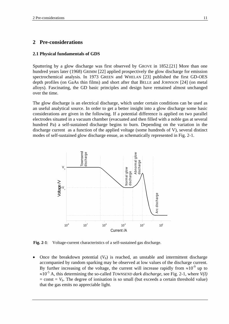
Sputtering by a glow discharge was first observed by GROVE in 1852.[21] More than one hundred years later (1968) GRIMM [22] applied prospectively the glow discharge for emission spectrochemical analysis. In 1973 GREEN and WHELAN [23] published the first GD-OES depth profiles (on GaAs thin films) and short after that BELLE and JOHNSON [24] (on metal alloys). Fascinating, the GD basic principles and design have remained almost unchanged over the time.
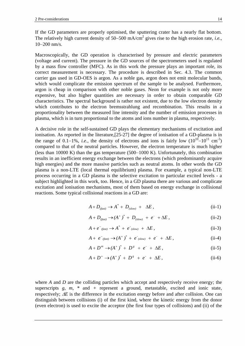
The glow discharge is an electrical discharge, which under certain conditions can be used as an useful analytical source. In order to get a better insight into a glow discharge some basic considerations are given in the following. If a potential difference is applied on two parallel electrodes situated in a vacuum chamber (evacuated and then filled with a noble gas at several hundred Pa) a self-sustained discharge begins to burn. Depending on the variation in the discharge current as a function of the applied voltage (some hundreds of V), several distinct modes of self-sustained glow discharge ensue, as schematically represented in Fig. 2-1.
Once the breakdown potential (Vb) is reached, an unstable and intermittent discharge accompanied by random sparking may be observed at low values of the discharge current. By further increasing of the voltage, the current will increase rapidly from 10-9 up to
10-5 A, this determining the so-called TOWNSEND dark discharge, see Fig. 2-1, where V(I) = const = Vb. The degree of ionisation is so small (but exceeds a certain threshold value) that the gas emits no appreciable light.
Fig. 2-1: Voltage-current characteristics of a self-sustained gas discharge.
10-9 10-7 10-5 10-3 10-1 101
Volta
ge /V
Current /A
Tow
nsen
ddi
scha
rge
Nor
mal
glo
wdi
scha
rge Abn
orm
al g
low
disc
harg
e
Arc
dis
char
ge
Vb
Vn
2 Pre-considerations 12
An increase of the current in the range of 10-5 10-3 A results in a decrease of the voltage down to a constant value Vn (see Fig. 2-1), this characterising a transition regime.
For large variations of the current from about 10-4 10-2 A the voltage Vn remains constant. In this so-called normal glow discharge regime, one can observe zones in the discharge body from which visible light is strongly emitted. However, the release of material from the cathode is negligible small so that only the spectrum of the gas is observed.
Further increase of the discharge current up to 10-1 A causes an increase of the voltage, this regime characterising the abnormal glow discharge. If for a normal GD, the current density at the cathode remains constant, the area sputtered at the cathode increasing with the current, for an abnormal GD an increase in current effects a rise of the current density and consequently an efficient sputtering.
Thermal electron emission from the cathode occurs when the current is further increased and the voltage drops significantly down to several tens of volts and the glow discharge is altered.
When the discharge current is 1 A, the glow discharge cascades to an arc discharge.
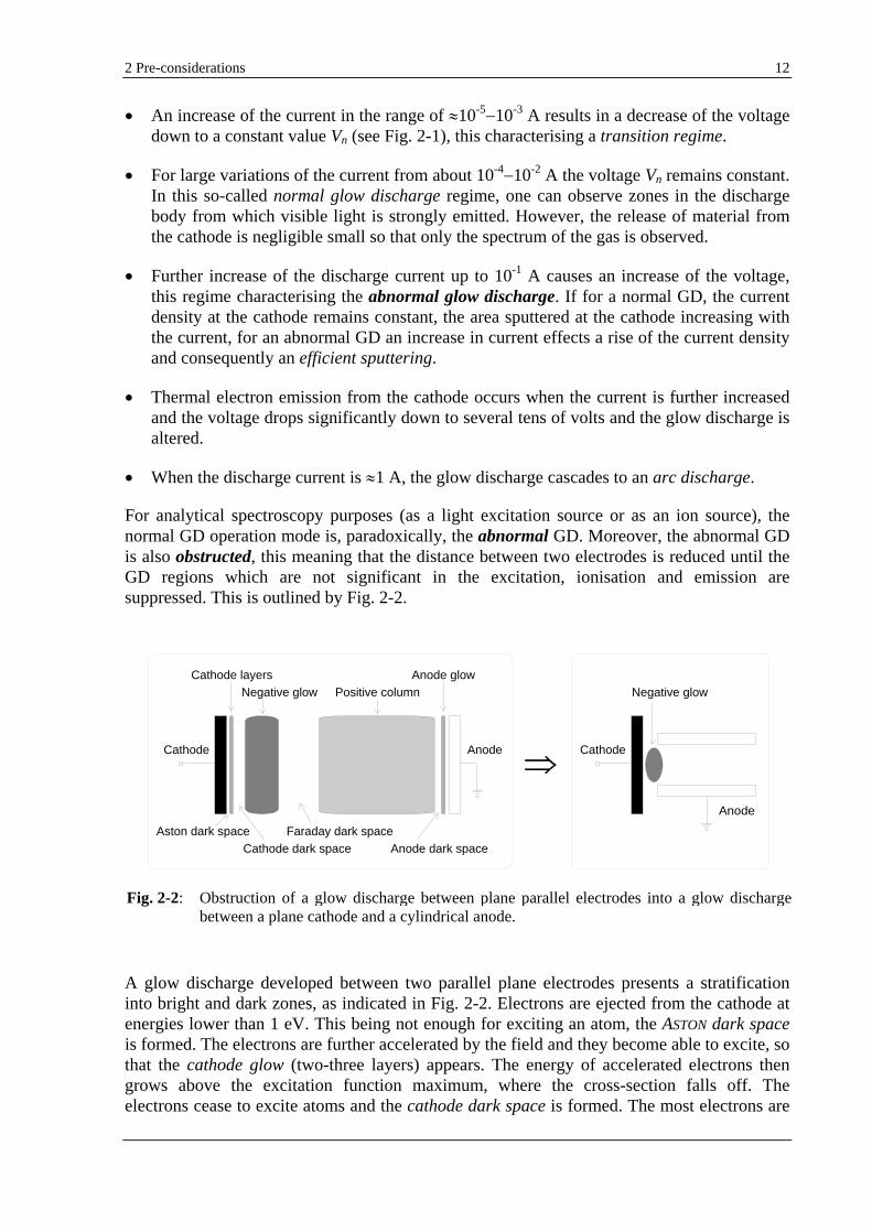
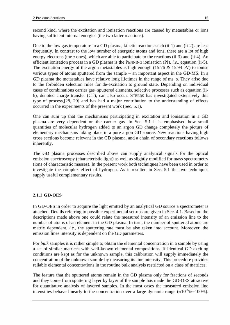
For analytical spectroscopy purposes (as a light excitation source or as an ion source), the normal GD operation mode is, paradoxically, the abnormal GD. Moreover, the abnormal GD is also obstructed, this meaning that the distance between two electrodes is reduced until the GD regions which are not significant in the excitation, ionisation and emission are suppressed. This is outlined by Fig. 2-2.
A glow discharge developed between two parallel plane electrodes presents a stratification into bright and dark zones, as indicated in Fig. 2-2. Electrons are ejected from the cathode at energies lower than 1 eV. This being not enough for exciting an atom, the ASTON dark space is formed. The electrons are further accelerated by the field and they become able to excite, so that the cathode glow (two-three layers) appears. The energy of accelerated electrons then grows above the excitation function maximum, where the cross-section falls off. The electrons cease to excite atoms and the cathode dark space is formed. The most electrons are
Fig. 2-2: Obstruction of a glow discharge between plane parallel electrodes into a glow discharge between a plane cathode and a cylindrical anode.
Anode
Anode
CathodeCathode
Positive columnNegative glow Negative glowCathode layers Anode glow
Aston dark spaceCathode dark space
Faraday dark spaceAnode dark space
2 Pre-considerations 13
multiplied in this region and the ionisation of atoms takes place predominantly here. A large positive space charge builds up. The field becomes weak and the electron energy decreases with increasing distance from the cathode, the electron energy being in the region of the maximum of the excitation function. Thus the negative glow appears, in its first part being excited the higher atomic levels and then lower ones. As the electrons dissipate their energy in the weak field excitations become less and less frequent. The negative glow gives way to the FARADAY dark space. The field increases further gradually and then remains constant. Electrons of 1-2 eV, but also high energy electrons coming from the cathode layer or even from the cathode can excite again atoms. Thus, the positive column is formed. The anode repels ions but pulls out electrons from the column. Therefore, a region of negative space charge is formed; its higher field accelerates electrons. The result is the anode glow.
If the interelectrode distance is reduced till it becomes just a few times the cathode dark space thickness, the positive column and the FARADAY dark space will disappear. It is clear that for analytical spectrochemistry an abnormal and obstructed glow discharge will supply an efficient sputtering as well as intense excitation and ionisation of the analytes. Therefore the change in geometry shown in Fig. 2-2 was an excellent finding in using of only the relevant part of a glow discharge, namely the negative glow. Moreover, the cylindrical form of the anode provides a possibility of axial observation (through a window to a optical spectrometer or to the ion optic of a mass spectrometer).
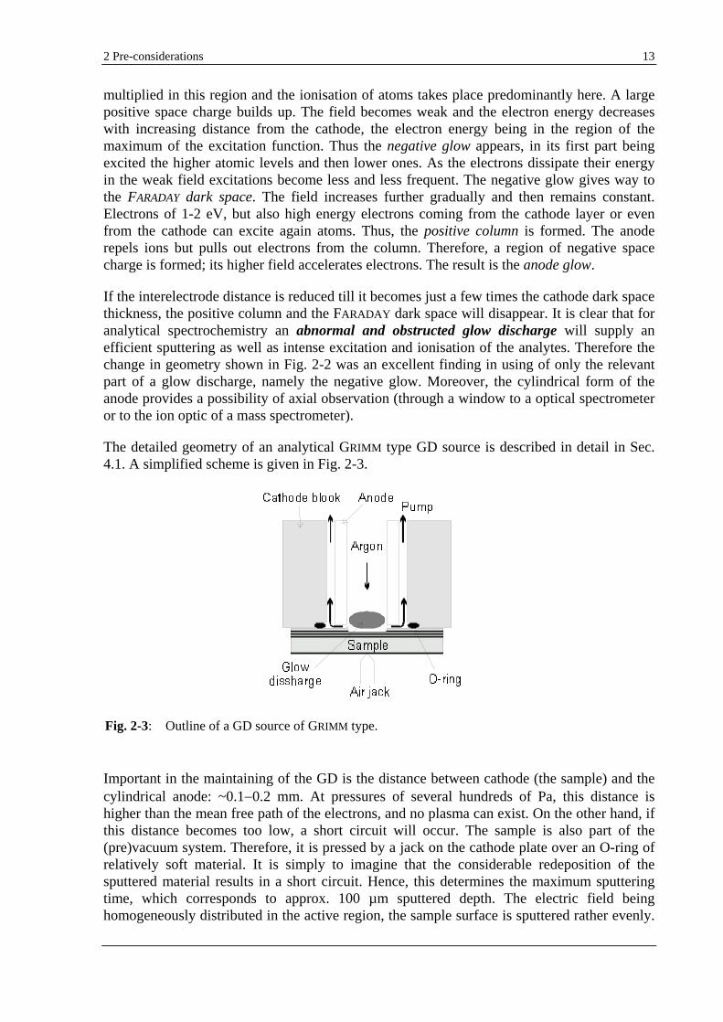
The detailed geometry of an analytical GRIMM type GD source is described in detail in Sec. 4.1. A simplified scheme is given in Fig. 2-3.
Important in the maintaining of the GD is the distance between cathode (the sample) and the cylindrical anode: ~0.1 0.2 mm. At pressures of several hundreds of Pa, this distance is higher than the mean free path of the electrons, and no plasma can exist. On the other hand, if this distance becomes too low, a short circuit will occur. The sample is also part of the (pre)vacuum system. Therefore, it is pressed by a jack on the cathode plate over an O-ring of relatively soft material. It is simply to imagine that the considerable redeposition of the sputtered material results in a short circuit. Hence, this determines the maximum sputtering time, which corresponds to approx. 100 µm sputtered depth. The electric field being homogeneously distributed in the active region, the sample surface is sputtered rather evenly.
Fig. 2-3: Outline of a GD source of GRIMM type.
2 Pre-considerations 14
If the GD parameters are properly optimised, the sputtering crater has a nearly flat bottom. The relatively high current density of 50 500 mA/cm2 gives rise to the high erosion rate, i.e., 10 200 nm/s.
Macroscopically, the GD operation is characterised by pressure and electric parameters (voltage and current). The pressure in the GD sources of the spectrometers used is regulated by a mass flow controller (MFC). As in this work the pressure plays an important role, its correct measurement is necessary. The procedure is described in Sec. 4.3. The common carrier gas used in GD-OES is argon. As a noble gas, argon does not emit molecular bands, which would complicate the emission spectrum of the sample to be analysed. Furthermore, argon is cheap in comparison with other noble gases. Neon for example is not only more expensive, but also higher quantities are necessary in order to obtain comparable GD characteristics. The spectral background is rather not existent, due to the low electron density which contributes to the electron bremsstrahlung and recombination. This results in a proportionality between the measured line intensity and the number of emission processes in plasma, which is in turn proportional to the atoms and ions number in plasma, respectively.
A decisive role in the self-sustained GD plays the elementary mechanisms of excitation and ionisation. As reported in the literature,[25-27] the degree of ionisation of a GD-plasma is in the range of 0.1 1%, i.e., the density of electrons and ions is fairly low (1010 1011 cm-3) compared to that of the neutral particles. However, the electron temperature is much higher (less than 10000 K) than the gas temperature (500 1000 K). Unfortunately, this combination results in an inefficient energy exchange between the electrons (which predominantly acquire high energies) and the more massive particles such as neutral atoms. In other words the GD plasma is a non-LTE (local thermal equilibrium) plasma. For example, a typical non-LTE process occurring in a GD plasma is the selective excitation to particular excited levels - a subject highlighted in this work, too. Hence, in a GD plasma there are various and complicate excitation and ionisation mechanisms, most of them based on energy exchange in collisional reactions. Some typical collisional reactions in a GD are:
E DADA (slow)*
(fast) , (ii-1)
E e D)(ADA -(slow)
*(fast)
, (ii-2)
E eAeA (slow)-*
(fast) , (ii-3)
E e e)(A eA -(slow)
-*(fast) , (ii-4)
E e D)(ADA -g*m , (ii-5)
E e D)(ADA -g* , (ii-6)
where A and D are the colliding particles which accept and respectively receive energy; the superscripts g, m, * and + represent a ground, metastable, excited and ionic state, respectively; E is the difference in the excitation energy before and after collision. One can distinguish between collisions (i) of the first kind, where the kinetic energy from the donor (even electron) is used to excite the acceptor (the first four types of collisions) and (ii) of the
2 Pre-considerations 15
second kind, where the excitation and ionisation reactions are caused by metastables or ions having sufficient internal energies (the two latter reactions).
Due to the low gas temperature in a GD plasma, kinetic reactions such (ii-1) and (ii-2) are less frequently. In contrast to the low number of energetic atoms and ions, there are a lot of high energy electrons (the ones), which are able to participate to the reactions (ii-3) and (ii-4). An efficient ionisation process in a GD plasma is the PENNING ionisation (PI), i.e., equation (ii-5). The excitation energy of the argon metastables is high enough (15.76 & 15.94 eV) to ionise various types of atoms sputtered from the sample
an important aspect in the GD-MS. In a GD plasma the metastables have relative long lifetimes in the range of ms s. They arise due to the forbidden selection rules for de-excitation to ground state. Depending on individual cases of combinations carrier gas sputtered elements, selective processes such as equation (ii-6), denoted charge transfer (CT), can also occur. STEERS has investigated extensively this type of process,[28, 29] and has had a major contribution to the understanding of effects occurred in the experiments of the present work (Sec. 5.1).
One can sum up that the mechanisms participating in excitation and ionisation in a GD plasma are very dependent on the carrier gas. In Sec. 5.1 it is emphasised how small quantities of molecular hydrogen added to an argon GD change completely the picture of elementary mechanisms taking place in a pure argon GD source. New reactions having high cross sections become relevant in the GD plasma, and a chain of secondary reactions follows inherently.
The GD plasma processes described above can supply analytical signals for the optical emission spectroscopy (characteristic light) as well as slightly modified for mass spectrometry (ions of characteristic masses). In the present work both techniques have been used in order to investigate the complex effect of hydrogen. As it resulted in Sec. 5.1 the two techniques supply useful complementary results.
2.1.1 GD-OES
In GD-OES in order to acquire the light emitted by an analytical GD source a spectrometer is attached. Details referring to possible experimental set-ups are given in Sec. 4.1. Based on the descriptions made above one could relate the measured intensity of an emission line to the number of atoms of an element in the GD plasma. In turn, the number of sputtered atoms are matrix dependent, i.e., the sputtering rate must be also taken into account. Moreover, the emission lines intensity is dependent on the GD parameters.
For bulk samples it is rather simple to obtain the elemental concentration in a sample by using a set of similar matrices with well-known elemental compositions. If identical GD exciting conditions are kept as for the unknown sample, this calibration will supply immediately the concentration of the unknown sample by measuring its line intensity. This procedure provides reliable elemental concentrations in the routine bulk analysis restricted on a class of matrices.
The feature that the sputtered atoms remain in the GD plasma only for fractions of seconds and they come from sputtering layer by layer of the sample has made the GD-OES attractive for quantitative analysis of layered samples. In the most cases the measured emission line intensities behave linearly to the concentration over a large dynamic range ( 10-4% 100%).
2 Pre-considerations 16
On the other hand, due to the very high erosion rate ( 10-200 nm/s), the depth resolution is slightly worse than that of other depth profiling techniques such as SNMS or SIMS. Nevertheless, the GD-OES depth profiling technique assumes the analyse of the whole sputtering crater. The other two methods either use a mask for reducing the crater effects (SNMS) or take into account only a reduced region in the centre of a presputtered crater (SIMS), respectively. Further discussions are given in Sec. 2.3, 5.2 and 6.2.
In the recent 15 years modern quantification algorithms have been developed and permanently improved by taking into account various effects: dependence on the plasma parameters, self-absorption, spectral interferences, or background corrections.[25, 30] Other effects such as the hydrogen effect, sample reflectivity, water cooling, etc,[31, 32] should be implemented as soon as possible. Thus, quantification of materials having various concentrations in various layered matrices is possible to perform by GD-OES. However, if the quantification of electrical conductive samples is successfully carried out in DC-GD-OES routine analysis, quite different is the case for non-conductive materials. The correct measurement of the electrical RF-GD parameters (of crucial importance in the GD-OES quantification) is still subject for further investigations.
2.1.1.1 DC-GD-OES quantification
The complex microscopical processes of sputtering, excitation and ionisation and de-excitation involved in the production of the analytical signals in a GD are very difficult to be measured accurately, i.e., directly in the GD plasma. The analyst can record the anode to cathode potential and current, the pressure (also not directly in the GD plasma), the sputtered depth and of course, the emission intensities. As the sputtering and the emission are not possible to be separated with respect to their quantitative dependence on voltage, current and pressure, empirical methods have been developed for quantification of the measured optical intensities. These three DC-GD parameters are not variably separately. Only two of them may be varied independently, the third one remaining dependent on the other two and on the sample matrix as well.
The basic concept in the GD-OES quantification is the emission yield. As used firstly by PONS-CORBEAU and BERNERON [33, 34] and many groups from Japan in the 80s and further by BENGTSON,[35-37] the emission yield is defined as the emitted light per unit sputtered mass of an element and per time unit. Hence, the emission intensity Ikl of the spectral line l of an element k is:
) / ( dtdm RI kklkl , (ii-7)
where dmk is unit sputtered mass of the element k and Rkl the emission yield of the spectral line l of the element k. The unit mass of an element sputtered per time unit in plasma (dmk / dt) is dependent on the concentration of the respective element, ck, in the sample. On the other hand, same concentrations of an element in different matrices could result in different line intensities, even under identical excitation conditions. Therefore, the sputtering rate q must be introduced:
kk cqdtdm / . (ii-8)
2 Pre-considerations 17
Expressed in µg/s, it characterises not a single element, but the instantaneous sputtering of the sample. Using eq. (ii-8) one can rewrite eq. (ii-7) in eq. (ii-9):
kklkl c q RI
. (ii-9)
Once the nature and composition of the sputtered matrix are included in eq. (ii-9), it is assumed that the emission yield is independent of the matrix. At least in a first approximation, this is largely confirmed in literature.[25] This fundamental equation can convert the measured emission line intensity of an element into the concentration of that element in the sample.
One could distinguish various GD-OES quantification algorithms developed quite close in time to each other, all of them being in fact based on the emission yield concept. In their concept, PONS-CORBEAU et al. [33, 34] used emission yield ratios. Thus, by ratioing eq. (ii-9) for two spectral lines of two different elements from the same sample it was possible to calculate concentrations even with the advantage of compensating the fluctuations in the excitation parameters. One should also note that the calculated concentrations are not absolute, but relative to that of an element, e.g., a major element. Moreover, the sputtered depth was possible to calculate only by supplementary measurement of erosion rates.
Groups of Japanese researchers calculated the elemental concentrations and the sputtered depth by the so-called method of integrated intensities. The concentration (in weight percent) is derived from measuring the all elements of significant concentration and ratioing to the total sputtered mass. By knowing the density it is then possible to extract the depth.
Also based on the concept of emission yield, an elegant method of GD-OES quantification of intensity normalisation was developed by BENGTSON et al.[35-37] The measured intensities are once normalised to the sputtering rates, so that the calibration curves look linearly (the slope being the emission yield):
kklrefsklkl c R )/q (q I d) (normaliseI , (ii-10)
where qs/qref is the sputtering rate of the calibration sample normalised to the sputtering rate of a reference sample. The elemental composition and the sputtering rate of an unknown sample can be calculated from this multimatrix calibration by simply summing of the intensities of all major elements and re-normalising the sum to 100% - in principle similar to the others methods presented above. One problem available for all different calibration methods described is the calculation of the density as being decisive in the determination of depth. The average density can be calculated by taking into account the concentrations of the pure elements in weight percent as well as in atom percent. Especially for oxides, nitrides and carbides, where the light elements are major constituents, the calculated densities are accurate to within 10%, but deviations up to 30% have been observed.[2]
On the other hand, one distinct feature of the quantification algorithm developed by BENGTSON is the possibility to carry out the quantification at arbitrary excitation parameters, i.e., the measured intensities are also normalise to a standard set of excitation conditions. Note that the sputtering rate q itself is also a function on the voltage and current, as BOUMANS
empirically measured:[38]
2 Pre-considerations 18
)( 0UU i Cq Q , (ii-11)
where U0 is the threshold voltage for an individual sample. One disputable point was which GD-parameters have a significant influence on the emission yield: voltage and current were considered by BENGTSON,[35, 37] contrary to PAYLING,[39] who considered the pressure as being the only one. In the meantime it is clarified [40] that pressure plays only a minor role in the variations of the emission yields. Systematic variations of the voltage and current at SIMR have resulted in empirical functions necessary to correct for the emission yields:
(U) f i C c k I kA
Qkklklk
, (ii-12)
where kkl is a line- and instrument specific constant, CQ is constant related to the sputtering rate, Ak is matrix independent constant, characteristic of spectral line k only and fk(U) is a polynomial of degree 1-3 with coefficients characteristic of spectral line k. The intensity-sputtering rate normalisation can be rather replaced by the concentration normalisation, i.e., the dependence of the intensities on concentrations multiplied by sputtering rates. E.g., background corrections can be better implemented. Hence, the DC-GD-OES quantification algorithm developed by BENGTSON is widely applicable for depth profile analysis, the procedure winning internationally recognition.
2.1.1.2 RF-GD
DC-GD-OES is unfortunately restricted to analysis of electrically conductive samples. Dielectrics can not be sputtered by DC-GD-OES due to charge effects on the surface of the sample. By applying a high frequency voltage on the so-called backing electrode, WEHNER et al. [41] demonstrated in 1962 that GD-sputtering of electrically non-conductive samples is also possible. Twelve years later COBURN et al. [42] used the GD for elemental analysis of non-conductive materials, however in combination with MS.
The first analytical RF-GD sources for OES were patented relative recently by PASSETEMPS et al. [43] (from the conventional GRIMM type) in 1988 and MARCUS [44] (similar to the sources used in AAS and which can be also used for MS) in 1989. In both versions a matching network is used to maximise the rf power transfer from the rf generator to the sample. Since the matching box serves unfortunately as a supplementary series capacitor for capacitive coupling, another approach was developed at IFW DRESDEN by HOFFMANN et al.[1] In this case the GD source is part of the rf oscillator circuit, also known as the free-running generator version. By its capability to analyse glasses, ceramics, lacquers, paints, organic coatings, but conductive materials, too, RF-GD-OES offers a new course to the solid sample analytical techniques, which makes it very attractive for a large variety of industrial applications.[45-56]
It is well-known that if a negative dc voltage is applied on the backside of a non-conductive sample, the potential at the sample surface will firstly drop down to the applied voltage value and then follow the charging function of a capacitor. Thus, due to the accumulation of positive charges at the surface and the electron loss through ion neutralisation reactions at the surface, no current can flow. If a high-frequency voltage is applied, the surface charging is alternatingly neutralised. However, due to the higher mobility of the plasma electrons compared to the much heavier positive ions, a more efficient neutralisation takes place during
2 Pre-considerations 19
the positive half-cycle. Thus, after approximately 3400 rf-periods, this meaning ~0.2 ms, a steady-state offset is established.[57, 58]
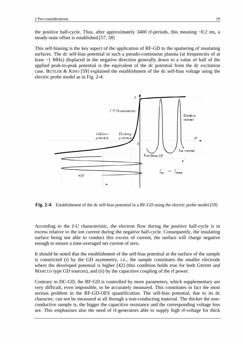
This self-biasing is the key aspect of the application of RF-GD to the sputtering of insulating surfaces. The dc self-bias potential in such a pseudo-continuous plasma (at frequencies of at least ~1 MHz) displaced in the negative direction generally down to a value of half of the applied peak-to-peak potential is the equivalent of the dc potential from the dc excitation case. BUTLER & KINO [59] explained the establishment of the dc self-bias voltage using the electric probe model as in Fig. 2-4:
According to the I-U characteristic, the electron flow during the positive half-cycle is in excess relative to the ion current during the negative half-cycle. Consequently, the insulating surface being not able to conduct this excess of current, the surface will charge negative enough to ensure a time-averaged net current of zero.
It should be noted that the establishment of the self-bias potential at the surface of the sample is constricted (i) by the GD asymmetry, i.e., the sample constitutes the smaller electrode where the developed potential is higher [42] (this condition holds true for both GRIMM and MARCUS type GD sources), and (ii) by the capacitive coupling of the rf power.
Contrary to DC-GD, the RF-GD is controlled by more parameters, which supplementary are very difficult, even impossible, to be accurately measured. This constitutes in fact the most serious problem in the RF-GD-OES quantification. The self-bias potential, due to its dc character, can not be measured at all through a non-conducting material. The thicker the non-conductive sample is, the bigger the capacitive resistance and the corresponding voltage loss are. This emphasises also the need of rf-generators able to supply high rf-voltage for thick
Fig. 2-4: Establishment of the dc self-bias potential in a RF-GD using the electric probe model.[59]
2 Pre-considerations 20
non-conductive samples. Also very difficult to measure is the rms current in the rf source, because the rf active current is superimposed by a much higher reactive current caused by the capacities of the GD source and the plasma.[1] One method used to measure the dc bias potential is, e.g., the insertion of an electrical probe through the O-ring seal directly onto the sample surface.[57] Dividing the measured rf-power by the dc-bias potential semiquantitative estimates are obtained for the rms current.[60]
In the approach reminded above of the free-running system of HOFFMANN et al. it is possible to measure the rf-power by multiplying the measured rf voltage and rf current in the nearest vicinity of the GD. This is a reliable alternative to the rf-power measurement based on the reflectometer principle, used by other authors. Also used in the present work, the HOFFMANN
rf system provides fast, stable, reliable and easy measurements as known in the dc operation mode.
Unfortunately, due to the inaccuracy in the measurement of some RF-GD parameters, the RF-GD-OES quantification is not so straightforward as in the DC-case. Various trials of rf-quantification algorithms were developed with limited success: use of a deconvolution procedure based on the measurement of the final sputtering crater;[61, 62] use of an electrical parameter and an Ar emission line;[63, 64] taking into account of the oscillations of the emission line intensities due to the interference effect for transparent layers (however only for determination of thickness). Promising work devoted to the accurate measuring of the rf-voltage, -current and -power is in progress in IFW DRESDEN.[65]
Nevertheless, qualitative RF-GD-OES depth profiling is very useful in analysing layered non-conductive materials. One can check for the presence of an element or to in-depth resolve a multilayered structure. Several examples of RF-GD-OES depth profiling of relevant non-conductive coatings on glass are presented in Sec. 6.2. It will be shown that the RF-GD-OES depth resolution is similar to that of other depth profiling techniques. Additionally, the high sputtering rate makes RF-GD-OES a powerful tool for non-conductive coated materials.
2.1.2 GD-MS
The GD has been known as an ion source for mass spectrometry for over 50 years. As in GD-OES, in GD-MS the conducting sample acts as the cathode and the plasma cell as the anode of a dc-plasma. Atoms are sputtered from the sample surface by argon ion bombardment and are then ionised in the GD-plasma. The ions - which constitutes the analytical signal in GD-MS - are extracted from the GD cell through the ion exit aperture and accelerated into a mass spectrometer. Rf coupling makes also possible the analyse of non-conductive bulk solid samples.[66] The technique of mixing an isolator with a conductive material in powder form, i.e., analysable in dc-mode, is still actual. GD-MS depth profiling [67-69] and rf-powering are subjects in progress. The strength of the method lies in its high sensitivity, trace elements in ng/g range being possible to be detected.
In this work prospective investigations regarding the effect of hydrogen on the analytical lines were carried out by means of GD-MS, see Sec. 5.1.4. The performed experiments have confirmed some assumptions resulted from the GD-OES results. On the other hand, these additional GD-MS experiments make clear that complementary pictures come out from GD-OES and -MS with respect to the hydrogen effect.
2 Pre-considerations 21
Since the GD-MS investigations are not the main point of this work the method is briefly described here. A special GD-MS design, based on the fast-flow concept, developed very recently in IFW DRESDEN by HOFFMANN et al. [70] was used. The GD source is based on the GRIMM type geometry (see also Sec. 4.2). The mass spectrometer is a low-resolution one containing a quadrupole and a SEM (secondary electrons multplier) and a FARADAY cup, respectively. In order to increase the ion signal entering the mass spectrometer a supplementary flowing channel was enclosed. Hence, if a potential difference of 600 1500 V is applied between the electrodes, at typically pressures of 300 1300 Pa, a current of 10-150 mA establishes, i.e., comparable GD parameters with those known from OES.
Some common bulk samples such as pure copper and titanium were used to prospect the hydrogen effect. Argon was used as the conventional carrier gas, but also neon was tested. Significant improvements with respect to the contamination were achieved by using of neon.
2.2 State-of-the-art of the analysis of light elements (H, C, N, O) (i) as contamination and (ii) as a sample constituent
It is well known that light elements are a serious problem generally available in the analysis of solid materials. Contamination of the sample surface is still present even after complex sample preparation procedures. Just as a relevant example, at 10-4 Pa a monolayer of contamination deposits in only 1 second.[71] Especially for analytical techniques, which need working pressures higher than in the UHV (ultra high vacuum) range, contamination such as water vapours, hydrocarbons, nitrogen, oxygen or carbon dioxide are always more or less present at the sample surface, but also on the walls of the analytical vacuum cell. Potential contaminants sources typically for a GD source are:
moisture at the sample surface, at the GD source walls or in the carrier gas, due to the absence of any sample preparation and the necessary opening of the GD source prior to a measurement;
backstreaming of gaseous hydrocarbons from pre-vacuum oil-pumps;
air leaks at the O-ring seal, open porosity or microcracks in the sample.
Most part of this contamination can be reduced by long pre-pumping and flushing times as well as by pre-burning times. However, for depth profiling of layered structures and especially for thin films the latter procedure can not be applied. ANGELI et al. [72] reported about the dependence of signal intensities on the pre-pumping time. O, N, H decreased, while C increased with the pumping time. These anomalies were explained by a dehydration and desorption of the sample surface from gases in the first case and by a back-diffusion of hydrocarbons from the vacuum system to the GD source. A clear decrease with pumping time of analytes such as Mn and Al as steel alloy elements was observed and put together with the presence of increased contamination in the GD source.
Generally, the contamination is present in molecular gaseous form. After switching-on the GD, a considerable reduction of the contamination will take place by sputtering and subsequent dissociating/cracking. The resulted atoms of light elements such as H, C, N, O can be sensitively detected by a VUV-VIS polychromator. Hence, GD-contamination can be easily distinguished by its exponential decrease in a depth profile. Actually, the presence of
2 Pre-considerations 22
contamination in the GD source is not directly the biggest problem, the GD-OES instrumentation being able to monitor it rather accurately. The real problem is the effect of gaseous contamination on the analytical signals, which are considerable even when very small quantities of contamination is present. Following effects can occur:
Co-excitation and competitive excitation of emission lines of the contaminants; thus, severe alterations in the whole excitation and ionisation mechanisms take place;
Excitation of emission band spectra or even of continuum spectra of molecular contaminating species, which superimpose the analytical atomic emission lines;
Alteration of the sputtering process, reactive sputtering and formation of a (e.g., oxide) thin film at the sample surface;[73]
Chemical reactions between the sputtered and the contaminating species in the GD plasma;[74, 75]
Change of the current as the dependent GD parameter.[7, 8]
FISCHER et al. [7, 8] investigated the effect of the addition of nitrogen and oxygen on the analytical parameters of GD-OES. They have empirically established upper thresholds for the content of nitrogen and oxygen in an argon GD of ~0.1 mass-%. Hence, working within this limit, the analytical signals are only slightly affected, if at all. It is shown, that the sputtering rate, the emission intensity of several spectral lines and the electrical current in a GD generally decrease for bulk samples of pure metals such as Al, Ti, Fe, Ni, Cu and Ag.
GD-OES investigations of compacted copper powder pellets exhibited intensive emission band spectra superimposed on the line spectra of the sample components,[76-79] due to the penetration of air into the excitation atmosphere. Therefore, a special device called "cap" was successfully used to prevent such air leakage.
Extensive works reported in the GD-OES literature have demonstrated that, beside the GD plasma parameters or the source geometry, the emission spectrum features are determined by the nature of the discharge gas. Not only molecular contaminant gaseous such as oxygen and nitrogen, but also the addition of small quantities of various noble gases to the carrier gas (conventionally a noble gas, too) can cause considerable changes in the emission spectra from the samples sputtered by a GD. WAGATSUMA et al. [9-16] shown that such mixing of carrier gases can supply very helpful results of fundamental interest in the understanding of the excitation and ionisation mechanisms in the GD plasma. Light molecular gases present in the GD source, by their multitude of molecular excited states, including vibrational and rotational states, cause a lot of changes in the excitation and ionisation processes of the sputtered atoms and of the carrier gas, too. However, the decrease of the sputtering rate upon the addition of the molecular impurity does not necessarily result in a decrease of the intensities for all emission lines of the analytes. Therefore, it is expected that the quantitative changes in the mechanisms involved in the excitation and ionisation processes are individual to each system sputtered species/carrier gas.
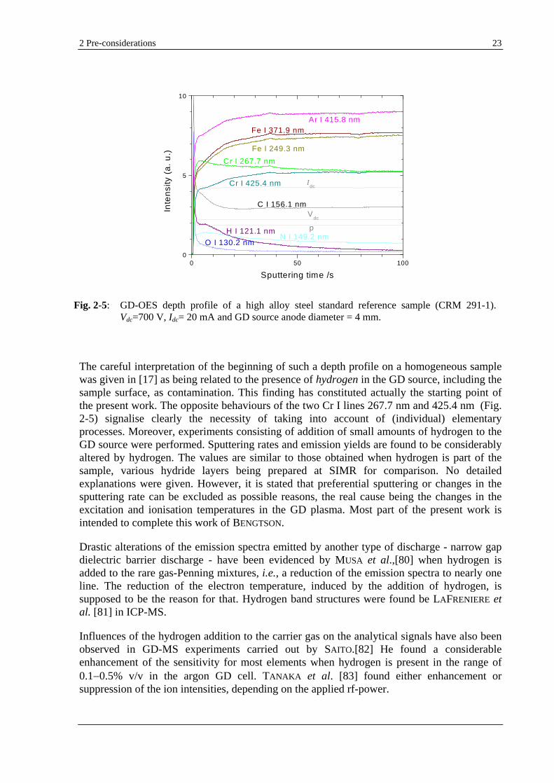
Recently, BENGTSON and HÄNSTRÖM [17] reported severe alterations of the analyte emission signals on analysis of steel and aluminium at the beginning of a depth profile, as being caused by the presence of contamination. A similar picture, which can be obtained by each GD-OES user, is presented in Fig. 2-5.
2 Pre-considerations 23
The careful interpretation of the beginning of such a depth profile on a homogeneous sample was given in [17] as being related to the presence of hydrogen in the GD source, including the sample surface, as contamination. This finding has constituted actually the starting point of the present work. The opposite behaviours of the two Cr I lines 267.7 nm and 425.4 nm (Fig. 2-5) signalise clearly the necessity of taking into account of (individual) elementary processes. Moreover, experiments consisting of addition of small amounts of hydrogen to the GD source were performed. Sputtering rates and emission yields are found to be considerably altered by hydrogen. The values are similar to those obtained when hydrogen is part of the sample, various hydride layers being prepared at SIMR for comparison. No detailed explanations were given. However, it is stated that preferential sputtering or changes in the sputtering rate can be excluded as possible reasons, the real cause being the changes in the excitation and ionisation temperatures in the GD plasma. Most part of the present work is intended to complete this work of BENGTSON.
Drastic alterations of the emission spectra emitted by another type of discharge - narrow gap dielectric barrier discharge - have been evidenced by MUSA et al.,[80] when hydrogen is added to the rare gas-Penning mixtures, i.e., a reduction of the emission spectra to nearly one line. The reduction of the electron temperature, induced by the addition of hydrogen, is supposed to be the reason for that. Hydrogen band structures were found be LAFRENIERE et al. [81] in ICP-MS.
Influences of the hydrogen addition to the carrier gas on the analytical signals have also been observed in GD-MS experiments carried out by SAITO.[82] He found a considerable enhancement of the sensitivity for most elements when hydrogen is present in the range of 0.1 0.5% v/v in the argon GD cell. TANAKA et al. [83] found either enhancement or suppression of the ion intensities, depending on the applied rf-power.
Fig. 2-5: GD-OES depth profile of a high alloy steel standard reference sample (CRM 291-1). Vdc=700 V, Idc= 20 mA and GD source anode diameter = 4 mm.
0 50 1000
5
10
p
Idc
Vdc
O I 130.2 nmN I 149.2 nm
H I 121.1 nm
C I 156.1 nm
Cr I 267.7 nm
Cr I 425.4 nm
Fe I 249.3 nm
Fe I 371.9 nmAr I 415.8 nm
Inte
nsi
ty (
a.
u.)
Sputtering time /s
2 Pre-considerations 24
Studies about the elementary processes taking place in an argon GD plasma using copper as a sample, when molecular gases containing hydrogen, such as methane or water are added, have been carried out by HESS and co-workers.[84-86] Despite using different values of GD parameters, quenching of the argon metastable atoms and inefficient sample sputtering have been found to be caused by reactions of water molecules or fragments with sputtered metal atoms in the gas phase by more researchers.[87-92] Supplementary investigations, such as MS, AAS or optical galvanic spectroscopy have confirmed many effects observed by GD-OES. PRINCE et al. [93] reported the emission of a hydrogen continuum when hydrogen was mixed with argon. Related to the sputtering suppression, TABARES and TAFALLA [94] suggested that the implantation of hydrogen in the metal surface is responsible for this.
So, one should distinguish, especially for GD-OES, between (i) the contamination of the sample by adsorption and hydration of the sample surface and in the near region and (ii) the contamination of the GD source at the walls and of the carrier gas. In the first case, care must be taken, because no sample preparation procedure is commonly used for GD-OES. The second kind of contamination can be reduced to a minimum by long pre-pumping, flushing and pre-burning time. However, for layered samples, pre-sputtering of pure materials like silicon wafers can successfully be used.
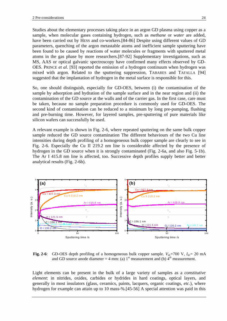
A relevant example is shown in Fig. 2-6, where repeated sputtering on the same bulk copper sample reduced the GD source contamination The different behaviours of the two Cu line intensities during depth profiling of a homogeneous bulk copper sample are clearly to see in Fig. 2-6. Especially the Cu II 219.2 nm line is considerable affected by the presence of hydrogen in the GD source when it is strongly contaminated (Fig. 2-6a, and also Fig. 5-1b). The Ar I 415.8 nm line is affected, too. Successive depth profiles supply better and better analytical results (Fig. 2-6b).
Light elements can be present in the bulk of a large variety of samples as a constitutive element: in nitrides, oxides, carbides or hydrides in hard coatings, optical layers, and generally in most insulators (glass, ceramics, paints, lacquers, organic coatings, etc.), where hydrogen for example can attain up to 10 mass-%.[45-56] A special attention was paid in this
Fig. 2-6: GD-OES depth profiling of a homogeneous bulk copper sample. Vdc=700 V, Idc= 20 mA and GD source anode diameter = 4 mm: (a) 1st measurement and (b) 4th measurement.
0 50 1000
1
2
3
4
5
(b)
O I 130.2 nm N I 149.2 nm
C I 156.1 nmH I 121.5 nm
p
Vdc
Ar I 415.8 nm
Cu II 219.2 nm
Cu I 327.3 nm
Idc
Inte
nsi
ty (
a.
u.)
Sputtering time /s
0 50 1000
1
2
3
4
5
(a)
p
Idc
C I 156.1 nm
Cu II 219.2 nmCu I 327.3 nm
O I 130.2 nm
N I 149.2 nm
H I 121.5 nm
Ar I 415.8 nm
Vdc
Inte
nsi
ty (
a.
u.)
Sputtering time /s
2 Pre-considerations 25
work to electrolytical coatings. The detection of light elements, however in their atomic form, is actually not at all problematic by means of GD-OES, this is even a big advantage of the method. The real problem is the negative influence of these light elements on the analytical signals. This is what must be taken into account or corrected for, respectively, in the GD-OES quantification.
GD-OES quantification of hydrogen is rather impossible at this time, due to the lack of suitable CRMs containing hydrogen. The mobility of hydrogen even at ambient temperature is very high, i.e., 10-7 10-4 cm2/s,[19] and therefore the elemental composition of the sample remains unstable in time. Due to the lack of samples with well-known concentration of hydrogen, conductive pellets containing hydrides have been recently prepared in IFW DRESDEN for internal use only. It was reported that for various concentrations of hydrogen in a pellet, changes in the emission yield of many lines occur.[32] Special efforts are at present devoted to the production of commercial standard materials containing hydrogen (NIST, SIMR, IFW DRESDEN). Stoichiometric hydrated Ti (or TiAlCrV) alloys were preliminary produced as a coating at SIMR and IFW DRESDEN and investigated in this work. X-ray spectrometry measurements proved that the TiH2 layer produced in IFW DRESDEN is a crystalline phase.
2.3 Alternative methods selected for depth profiling of thin layers containing light elements (SNMS, SIMS, NRA)
In its unique combination of great speed, sensitivity and ease of quantification, GD-OES is a very attractive depth profiling method for the industry. For very thin films with a thickness down to 2-3 nm,[3] but especially for thick films, even of more than 100 µm, GD-OES has its strength relative to other analytical methods. Since the sputtering process depends strongly on matrix, depth profiling of alternating layers of different matrices needs an optimisation procedure as a prerequisite for reaching the best depth resolution.
Such empirical procedures are exemplified in the final part of this work. For electrically conductive materials the optimisation procedures are not time consuming and, in contrary, non-conductive materials may need very long testing times. The results can be used for matrix specific analysis and can be considered as a useful preliminary work for the future RF-GD-OES quantification. Hence, despite of the qualitative character of the RF-GD-OES depth profiling, it is shown that the method can supply valuable information in a short time (Sec. 5.2.2 and 6.2).[95, 96]
In order to evaluate the performances of the GD-OES in depth profiling of thin non-conductive materials, alternative analytical methods such as SNMS, SIMS and NRA have been comparatively tested for some relevant samples.
Considered as close to the GDS, in terms of sample sputtering with Ar ions from a plasma and separate post-ionisation of the sputtered neutrals (analogue to the excitation/ionisation of the sputtered atoms in the GD plasma), plasma SNMS is rather suitable for depth profiling of thin layers.[97-103] Very thin layers in the nm thickness range are well resolved, due to the different plasma parameters, e.g., the lower working pressure in the range of ~0.1 Pa, which result in a more "feathery" sputtering (somewhat similar to the very recently introduced pulsed GD excitation [104]) in comparison with the GD-OES case. Contrary to the GD
2 Pre-considerations 26
plasma, the SNMS plasma is maintained at electron cyclotron resonance by inductive coupling of a high frequency (27.12 MHz). Experimental details are given in Sec. 4.4. It should be noted that plasma SNMS was used in this work. This means that this plasma supplies Ar ions as a primary ion source for sputtering and it also serves as a post-ionisation medium. The sputtered neutrals could be for example ionised by a laser (LI-SNMS). Excellent plasma SNMS depth resolution can be reached for coatings up to several µm. However, due to the very low sputtering rates, the necessary analysis time is very long, i.e., at least ~5 hours (for non-conductive materials) together with sample preparation and transfer chamber evacuation.
Also based on the principle of sputtering with primary ions is SIMS. In this work ToF-SIMS measurements have been performed on electrically non-conductive multilayer materials.[6, 95] Experimental details on the instrumentation existent in BAM are given in Sec. 4.5. Due to the typical low sputtering rate, the samples were cross-sectioned and a depth profile was obtained in an alternative way. An acceptable depth-resolution and a typical high sensitivity for alkali metals, for example can be often very useful. Direct depth profiling can be successfully applied for thin layers, electrically conductive as well as non-conductive by charge compensation techniques.
An analytical technique rather different from the operating principles of GD-OES, but used as a powerful tool in hydrogen detection in coated materials is Nuclear Reaction Analysis (NRA).[105, 106] Based on the resonance nuclear reaction with irradiated 15N ions, the amount and the depth distribution of hydrogen can be obtained mainly in thin layers. Depending on the materials investigated maximum depths of 1-2 µm can be prospected. However, large uncertainties can result from the interpretation of the experimental data. Hydrogen concentrations of up to 3 at.-% in DLC layers and up to 1.6 at.% in pure Si3N4
layers or even up to 9 at.-% in films containing oxygen have been found and reported in the literature.[107-109]
3 Objectives 27
3 Objectives
Two major aspects are resulted from PRE-CONSIDERATIONS as being subjects for further investigations performed in the present work:
i. the capability of GD-OES to analyse hydrogen, however under appropriate fundamental considerations, and
ii. GD-OES depth profiling of thick coatings containing hydrogen, as well as of thin and very thin coatings. The later ones are mostly electrically non-conductive, and do not contain necessary hydrogen, but the contamination (mainly hydrogen) plays a crucial role.
As far as the hydrogen analysis is concerned, GD-OES presents an unique combination of rapidity, very low DL (1 µg/g for the H I 121.5 nm line) and maximal investigated depth of more than 100 µm. However, due to the lack of suitable CRMs containing hydrogen, a reliable GD-OES quantification of hydrogen is not possible yet. In order to overcome this problem, investigations on the simulation of a hydrogen calibration curve by adding hydrogen in gaseous form to the noble carrier GD gas could be taken account as an alternative. Section 5.1 is extensively devoted to this objective. Preliminary results reported recently in literature [17] highlighted considerable alterations in the sputtering rate and in the emission yield of some investigated emission lines. The effect was similar independent of the hydrogen source, i.e., when hydrogen is a sample constituent or a gaseous contamination. Further experiments in order to clarify this point are performed in this work (Sec. 5.1.6 and 6.3.2).
Not only the analysis of the hydrogen itself, but also the strong matrix effect of hydrogen must be corrected in the GD-OES quantification algorithms. Therefore, due to the complexity of the effect, fundamental investigations on elementary processes of excitation and ionisation in GD plasma are necessary. The well-known and simple emission spectra of copper will be taken into account and extensively investigated together with that of the carrier gas (Sec 5.1.1 and 5.1.2). Because the hydrogen effect is individual for each emission line, various analytes in common bulk materials are investigated (Sec. 5.1.4). As a key point in the understanding and explanation of the processes involved when hydrogen is present in a GD is proved to be the hydrogen emission continuum (Sec. 5.1.3). Comparisons of various sources of hydrogen relative to the hydrogen continuum should also be performed, inaccuracy in the measurements of the analytes being able to occur for analyte lines from a sputtered material containing hydrogen. Supplementary experiments related to the hydrogen effect in a GD are also carried out by means of GD-MS (Sec. 5.1.4) in order to confirm/complete the hypothesis found by GD-OES. Also the use of different carrier gases (Ar and Ne) can help to a better understanding of the effect. As a prerequisite for the correction of the hydrogen effect in the quantification algorithms, the dependence of the effect on the GD parameters must be taken into account (Sec. 5.1.9).
Thin films and thick coatings produced by various deposition methods, such as electroplating, CVD, PVD, laser arc deposition, etc., often contain hydrogen in unwanted concentrations in the coating, in the substrate or at their interface. Hydrogen is also known as easily penetrating many metals. Section 6.3 is intended to emphasise some of the hydrogen problematic encountered on materials from industrial applications by means of GD-OES. Heat treatment
3 Objectives 28
procedures applied in order to force hydrogen to diffuse out from the material need an analytical proof to control such processes. Even if not quantitatively, GD-OES analysis of hydrogen could prove as being very useful.
Depth profiling of electrically non-conductive multilayer coatings constitutes an analytical task for very few techniques. In order to establish the performances of GD-OES, a comparative study comprising three competitive analytical methods, i.e., RF-GD-OES, HFM plasma SNMS and ToF-SIMS, is subject of Sec. 6.2. Some relevant materials, largely used in the industry, such as SiO2, TiO2, Si3N4 multilayers deposited on glass or ceramics are considered as samples for the comparison. The limitations of the analytical methods relative to the analysis of such multilayer non-conductive materials are well-known. Optimisation procedures, known as very costly for layered non-conductive materials, will also be extensively investigated (Sec. 5.2 and 6.2) and compared for different competitive depth profiling techniques.
Knowing the multiple facets of the hydrogen effect, experiments of improving analytical figures of merit can be imaged by the controlled addition of small quantities of hydrogen to an argon GD plasma. Improvement of the, e.g., sensitivity, detection limits and depth profiling will be studied (Sec. 6.1 and 6.2) for some relevant examples.
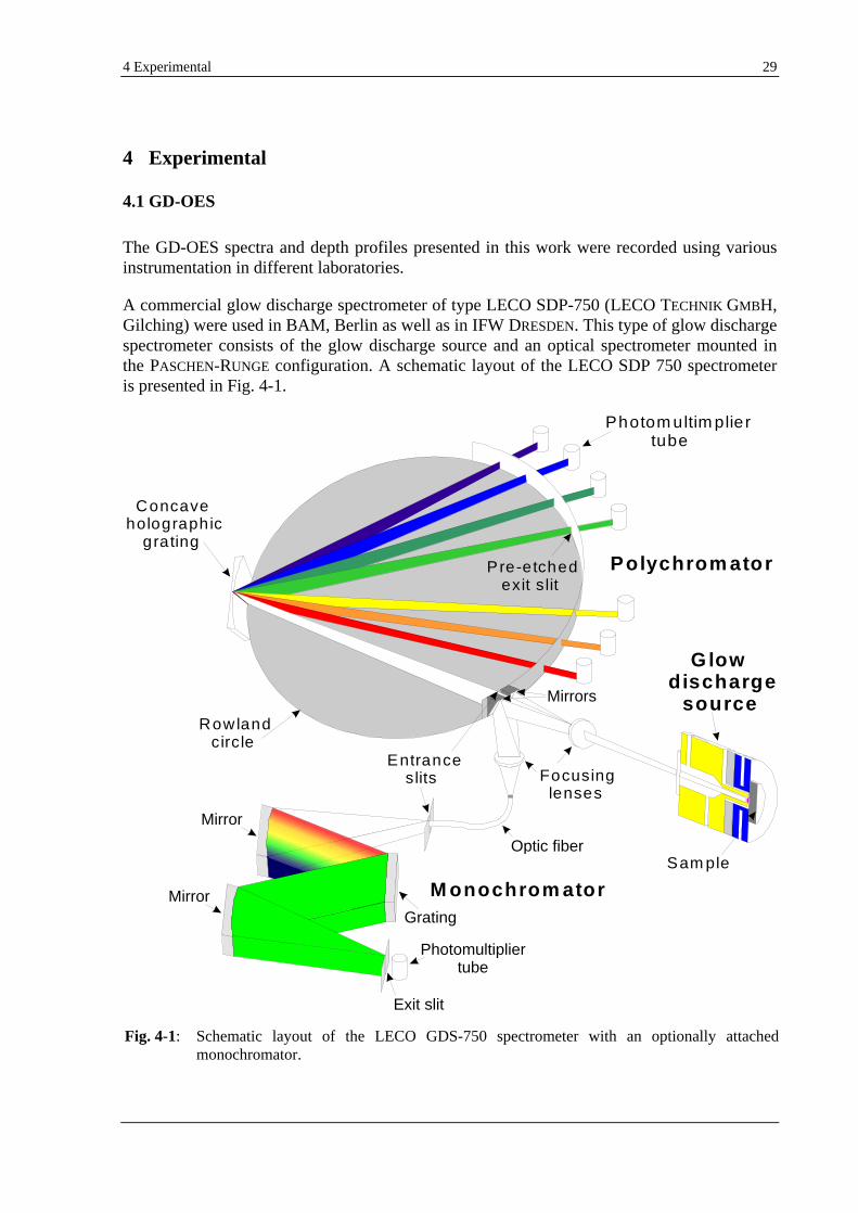
4 Experimental 29
4 Experimental
4.1 GD-OES
The GD-OES spectra and depth profiles presented in this work were recorded using various instrumentation in different laboratories.
A commercial glow discharge spectrometer of type LECO SDP-750 (LECO TECHNIK GMBH, Gilching) were used in BAM, Berlin as well as in IFW DRESDEN. This type of glow discharge spectrometer consists of the glow discharge source and an optical spectrometer mounted in the PASCHEN-RUNGE configuration. A schematic layout of the LECO SDP 750 spectrometer is presented in Fig. 4-1.
Fig. 4-1: Schematic layout of the LECO GDS-750
spectrometer with an optionally attached monochromator.
Photom ultim plie rtube
Exit slit
Concaveholographic
grating
Rowlandcircle
Entranceslits Focusing
lenses
Glowdischarge
source
Pre-etchedexit slit
Sam ple
Photomultipliertube
Grating
Mirror
Mirror
Mirrors
Optic fiber
Polychrom ator
M onochrom ator
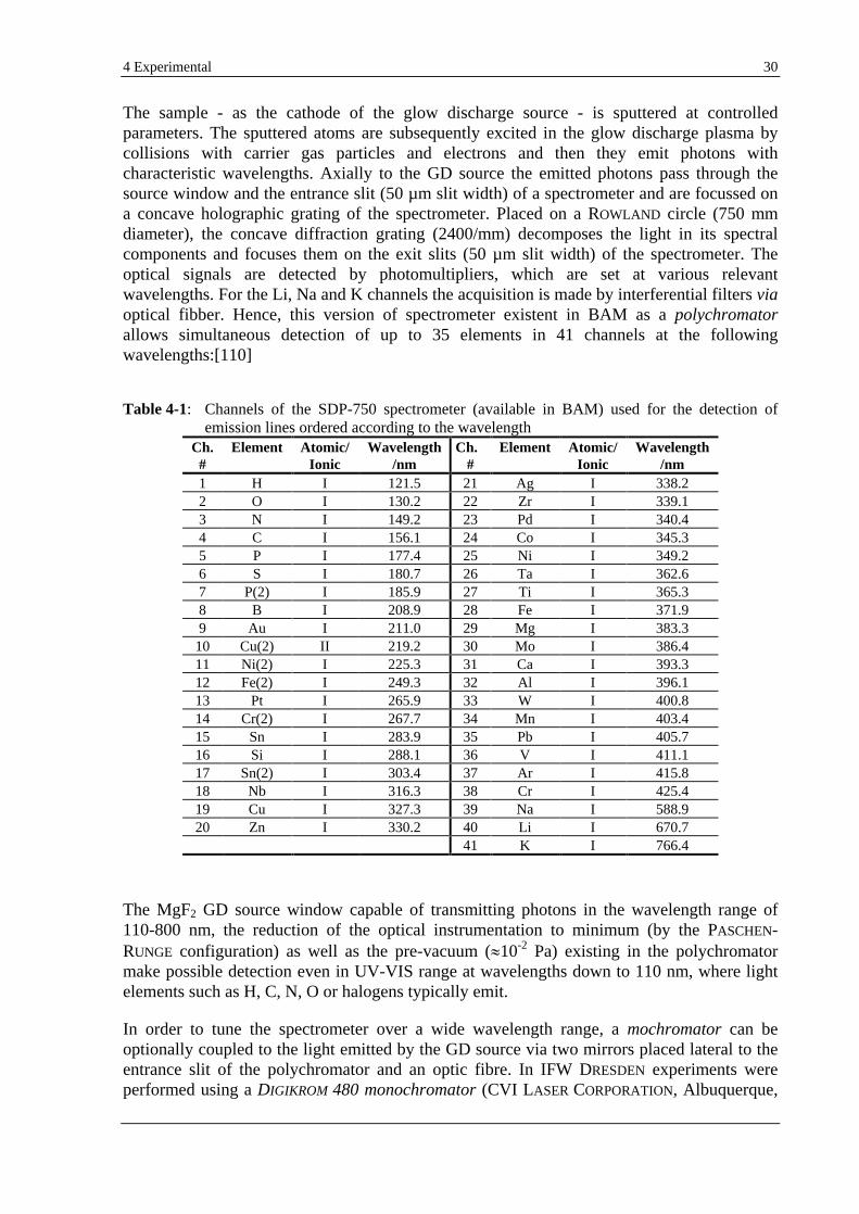
4 Experimental 30
The sample - as the cathode of the glow discharge source - is sputtered at controlled parameters. The sputtered atoms are subsequently excited in the glow discharge plasma by collisions with carrier gas particles and electrons and then they emit photons with characteristic wavelengths. Axially to the GD source the emitted photons pass through the source window and the entrance slit (50 µm slit width) of a spectrometer and are focussed on a concave holographic grating of the spectrometer. Placed on a ROWLAND circle (750 mm diameter), the concave diffraction grating (2400/mm) decomposes the light in its spectral components and focuses them on the exit slits (50 µm slit width) of the spectrometer. The optical signals are detected by photomultipliers, which are set at various relevant wavelengths. For the Li, Na and K channels the acquisition is made by interferential filters via optical fibber. Hence, this version of spectrometer existent in BAM as a polychromator allows simultaneous detection of up to 35 elements in 41 channels at the following wavelengths:[110]
Table 4-1: Channels of the SDP-750 spectrometer (available in BAM) used for the detection of emission lines ordered according to the wavelength
Ch. #
Element Atomic/ Ionic
Wavelength /nm
Ch. #
Element Atomic/ Ionic
Wavelength /nm
1 H I 121.5 21 Ag I 338.2 2 O I 130.2 22 Zr I 339.1 3 N I 149.2 23 Pd I 340.4 4 C I 156.1 24 Co I 345.3 5 P I 177.4 25 Ni I 349.2 6 S I 180.7 26 Ta I 362.6 7 P(2) I 185.9 27 Ti I 365.3 8 B I 208.9 28 Fe I 371.9 9 Au I 211.0 29 Mg I 383.3
10 Cu(2) II 219.2 30 Mo I 386.4 11 Ni(2) I 225.3 31 Ca I 393.3 12 Fe(2) I 249.3 32 Al I 396.1 13 Pt I 265.9 33 W I 400.8 14 Cr(2) I 267.7 34 Mn I 403.4 15 Sn I 283.9 35 Pb I 405.7 16 Si I 288.1 36 V I 411.1 17 Sn(2) I 303.4 37 Ar I 415.8 18 Nb I 316.3 38 Cr I 425.4 19 Cu I 327.3 39 Na I 588.9 20 Zn I 330.2 40 Li I 670.7
41 K I 766.4
The MgF2 GD source window capable of transmitting photons in the wavelength range of 110-800 nm, the reduction of the optical instrumentation to minimum (by the PASCHEN-RUNGE configuration) as well as the pre-vacuum ( 10-2 Pa) existing in the polychromator make possible detection even in UV-VIS range at wavelengths down to 110 nm, where light elements such as H, C, N, O or halogens typically emit.
In order to tune the spectrometer over a wide wavelength range, a mochromator can be optionally coupled to the light emitted by the GD source via two mirrors placed lateral to the entrance slit of the polychromator and an optic fibre. In IFW DRESDEN experiments were performed using a DIGIKROM 480 monochromator (CVI LASER CORPORATION, Albuquerque,
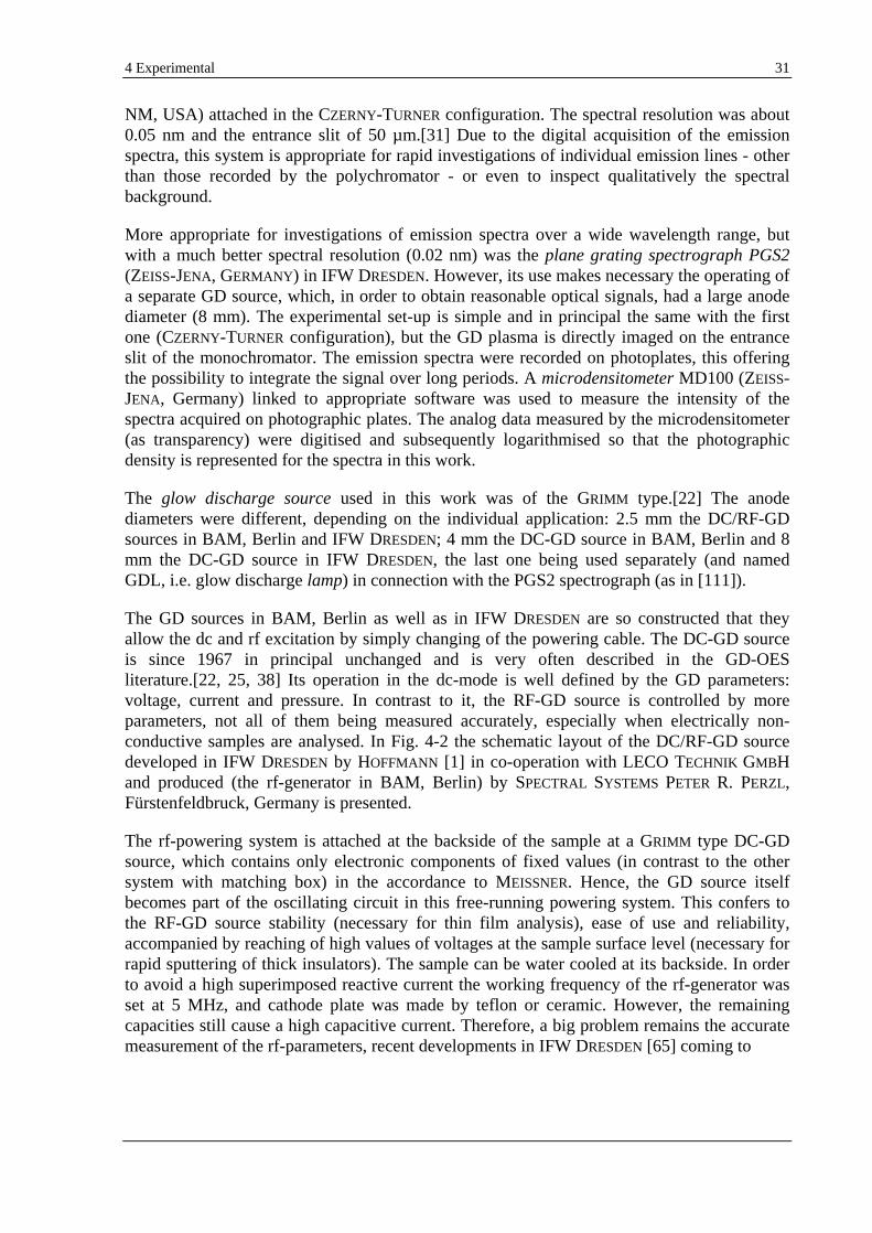
4 Experimental 31
NM, USA) attached in the CZERNY-TURNER configuration. The spectral resolution was about 0.05 nm and the entrance slit of 50 µm.[31] Due to the digital acquisition of the emission spectra, this system is appropriate for rapid investigations of individual emission lines - other than those recorded by the polychromator - or even to inspect qualitatively the spectral background.
More appropriate for investigations of emission spectra over a wide wavelength range, but with a much better spectral resolution (0.02 nm) was the plane grating spectrograph PGS2 (ZEISS-JENA, GERMANY) in IFW DRESDEN. However, its use makes necessary the operating of a separate GD source, which, in order to obtain reasonable optical signals, had a large anode diameter (8 mm). The experimental set-up is simple and in principal the same with the first one (CZERNY-TURNER configuration), but the GD plasma is directly imaged on the entrance slit of the monochromator. The emission spectra were recorded on photoplates, this offering the possibility to integrate the signal over long periods. A microdensitometer MD100 (ZEISS-JENA, Germany) linked to appropriate software was used to measure the intensity of the spectra acquired on photographic plates. The analog data measured by the microdensitometer (as transparency) were digitised and subsequently logarithmised so that the photographic density is represented for the spectra in this work.
The glow discharge source used in this work was of the GRIMM type.[22] The anode diameters were different, depending on the individual application: 2.5 mm the DC/RF-GD sources in BAM, Berlin and IFW DRESDEN; 4 mm the DC-GD source in BAM, Berlin and 8 mm the DC-GD source in IFW DRESDEN, the last one being used separately (and named GDL, i.e. glow discharge lamp) in connection with the PGS2 spectrograph (as in [111]).
The GD sources in BAM, Berlin as well as in IFW DRESDEN are so constructed that they allow the dc and rf excitation by simply changing of the powering cable. The DC-GD source is since 1967 in principal unchanged and is very often described in the GD-OES literature.[22, 25, 38] Its operation in the dc-mode is well defined by the GD parameters: voltage, current and pressure. In contrast to it, the RF-GD source is controlled by more parameters, not all of them being measured accurately, especially when electrically non-conductive samples are analysed. In Fig. 4-2 the schematic layout of the DC/RF-GD source developed in IFW DRESDEN by HOFFMANN [1] in co-operation with LECO TECHNIK GMBH and produced (the rf-generator in BAM, Berlin) by SPECTRAL SYSTEMS PETER R. PERZL, Fürstenfeldbruck, Germany is presented.
The rf-powering system is attached at the backside of the sample at a GRIMM type DC-GD source, which contains only electronic components of fixed values (in contrast to the other system with matching box) in the accordance to MEISSNER. Hence, the GD source itself becomes part of the oscillating circuit in this free-running powering system. This confers to the RF-GD source stability (necessary for thin film analysis), ease of use and reliability, accompanied by reaching of high values of voltages at the sample surface level (necessary for rapid sputtering of thick insulators). The sample can be water cooled at its backside. In order to avoid a high superimposed reactive current the working frequency of the rf-generator was set at 5 MHz, and cathode plate was made by teflon or ceramic. However, the remaining capacities still cause a high capacitive current. Therefore, a big problem remains the accurate measurement of the rf-parameters, recent developments in IFW DRESDEN [65] coming to
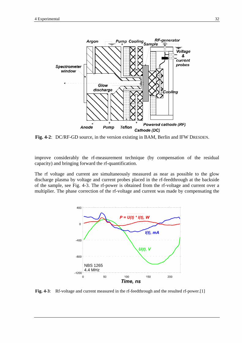
4 Experimental 32
improve considerably the rf-measurement technique (by compensation of the residual capacity) and bringing forward the rf-quantification.
The rf voltage and current are simultaneously measured as near as possible to the glow discharge plasma by voltage and current probes placed in the rf-feedthrough at the backside of the sample, see Fig. 4-3. The rf-power is obtained from the rf-voltage and current over a multiplier. The phase correction of the rf-voltage and current was made by compensating the
Fig. 4-2: DC/RF-GD source, in the version existing in BAM, Berlin and IFW DRESDEN.
Fig. 4-3: Rf-voltage and current measured in the rf-feedthrough and the resulted rf-power.[1]
NBS 12654.4 MHz
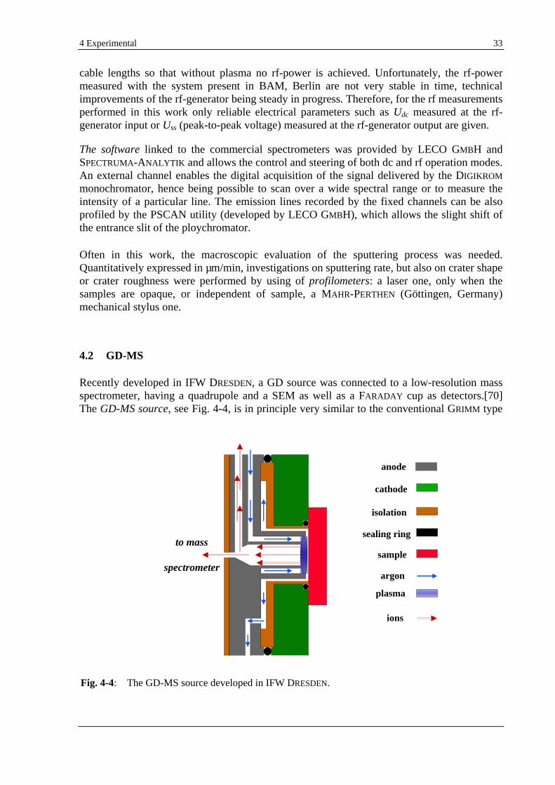
4 Experimental 33
cable lengths so that without plasma no rf-power is achieved. Unfortunately, the rf-power measured with the system present in BAM, Berlin are not very stable in time, technical improvements of the rf-generator being steady in progress. Therefore, for the rf measurements performed in this work only reliable electrical parameters such as Udc measured at the rf-generator input or Uss (peak-to-peak voltage) measured at the rf-generator output are given.
The software linked to the commercial spectrometers was provided by LECO GMBH and SPECTRUMA-ANALYTIK and allows the control and steering of both dc and rf operation modes. An external channel enables the digital acquisition of the signal delivered by the DIGIKROM
monochromator, hence being possible to scan over a wide spectral range or to measure the intensity of a particular line. The emission lines recorded by the fixed channels can be also profiled by the PSCAN utility (developed by LECO GMBH), which allows the slight shift of the entrance slit of the ploychromator.
Often in this work, the macroscopic evaluation of the sputtering process was needed. Quantitatively expressed in µm/min, investigations on sputtering rate, but also on crater shape or crater roughness were performed by using of profilometers: a laser one, only when the samples are opaque, or independent of sample, a MAHR-PERTHEN (Göttingen, Germany) mechanical stylus one.
4.2 GD-MS
Recently developed in IFW DRESDEN, a GD source was connected to a low-resolution mass spectrometer, having a quadrupole and a SEM as well as a FARADAY cup as detectors.[70] The GD-MS source, see Fig. 4-4, is in principle very similar to the conventional GRIMM type
Fig. 4-4: The GD-MS source developed in IFW DRESDEN.
anode
isolation
sealing ring
sample
argon
plasma
ions
to mass
spectrometer
cathode

4 Experimental 34
source used in GD-OES. However, in opposite to the GD-OES it is necessary to gain high ion signals for the mass spectrometric analyse. Therefore, an additional vacuum channel provides a high mass flow directed to the entrance of the mass spectrometer. Nevertheless, the GD-MS source works at comparable parameters to those known from GD-OES (Vdc= 600-1500 V, Idc= 10-150 mA and p= 300-1300 Pa for gas flows of 40-200 sccm argon or neon). This is an important aspect which enabled additional investigations with respect to the effect of hydrogen in a glow discharge, possible to be investigated by OES only partially. The instrumentation is also flexible, allowing working with various carrier gases and the connection of a gas mixing system, necessary for the experiments on the hydrogen effect. GD-MS provides lower detection limits and extends the list of elements to be GD-OES analysed. The GD-MS source used for the experiments in this work has a 10 mm diameter anode.
4.3 Hydrogen/carrier gas mixing system
A considerable part of this work was dedicated to the investigation of the effect of hydrogen in a glow discharge when hydrogen is present in the GD source as a gaseous contamination, i.e., added to the noble carrier gas into the GD source in defined concentrations. The flexibility of the system enabled its use for OES experiments in BAM, Berlin and IFW DRESDEN and for MS experiments in IFW DRESDEN. The scheme of the gas mixing system is shown in Fig. 4-5.
Pure argon coming from a cylinder through a mass flow controller (MFC) of maximum rate 2000 sccm was mixed over a T-piece with gas coming through another MFC of various maximum rates from a cylinder containing various volume concentrations of hydrogen and argon. The latter gas line was modified depending on the magnitude of the hydrogen effect in the GD source investigated in different experimental conditions, i.e., depending on the
Fig. 4-5: Schematic set-up of the gas mixing system.
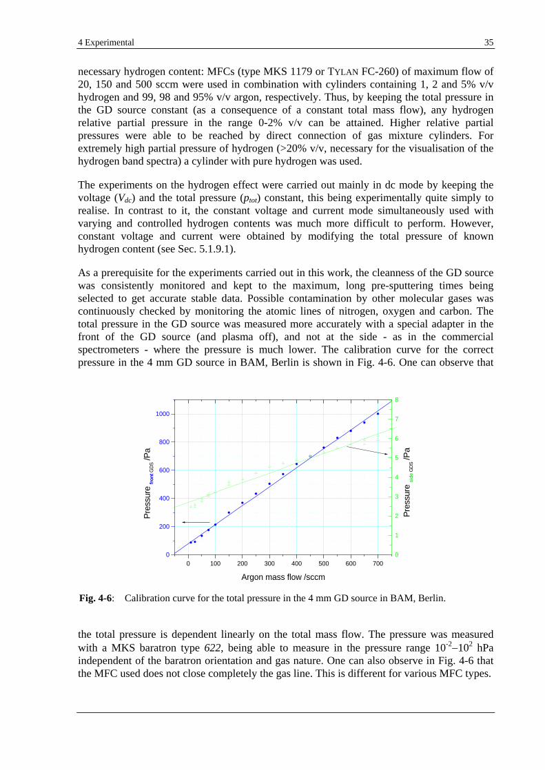
4 Experimental 35
necessary hydrogen content: MFCs (type MKS 1179 or TYLAN FC-260) of maximum flow of 20, 150 and 500 sccm were used in combination with cylinders containing 1, 2 and 5% v/v hydrogen and 99, 98 and 95% v/v argon, respectively. Thus, by keeping the total pressure in the GD source constant (as a consequence of a constant total mass flow), any hydrogen relative partial pressure in the range 0-2% v/v can be attained. Higher relative partial pressures were able to be reached by direct connection of gas mixture cylinders. For extremely high partial pressure of hydrogen (>20% v/v, necessary for the visualisation of the hydrogen band spectra) a cylinder with pure hydrogen was used.
The experiments on the hydrogen effect were carried out mainly in dc mode by keeping the voltage (Vdc) and the total pressure (ptot) constant, this being experimentally quite simply to realise. In contrast to it, the constant voltage and current mode simultaneously used with varying and controlled hydrogen contents was much more difficult to perform. However, constant voltage and current were obtained by modifying the total pressure of known hydrogen content (see Sec. 5.1.9.1).
As a prerequisite for the experiments carried out in this work, the cleanness of the GD source was consistently monitored and kept to the maximum, long pre-sputtering times being selected to get accurate stable data. Possible contamination by other molecular gases was continuously checked by monitoring the atomic lines of nitrogen, oxygen and carbon. The total pressure in the GD source was measured more accurately with a special adapter in the front of the GD source (and plasma off), and not at the side - as in the commercial spectrometers - where the pressure is much lower. The calibration curve for the correct pressure in the 4 mm GD source in BAM, Berlin is shown in Fig. 4-6. One can observe that
the total pressure is dependent linearly on the total mass flow. The pressure was measured with a MKS baratron type 622, being able to measure in the pressure range 10-2 102 hPa independent of the baratron orientation and gas nature. One can also observe in Fig. 4-6 that the MFC used does not close completely the gas line. This is different for various MFC types.
Fig. 4-6: Calibration curve for the total pressure in the 4 mm GD source in BAM, Berlin.
0 100 200 300 400 500 600 7000
200
400
600
800
1000
P
ress
ure
fron
t GD
S /P
a
Argon mass flow /sccm
0
1
2
3
4
5
6
7
8
Pre
ssur
e si
de G
DS
/Pa
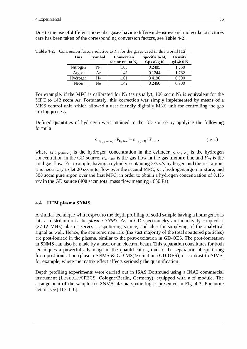
4 Experimental 36
Due to the use of different molecular gases having different densities and molecular structures care has been taken of the corresponding conversion factors, see Table 4-2.
Table 4-2: Conversion factors relative to N2 for the gases used in this work.[112] Gas Symbol Conversion
factor rel. to N2
Specific heat, Cp cal/g K
Density, g/l @ 0 K
Nitrogen N2 1.00 0.2485 1.250 Argon Ar 1.42 0.1244 1.782
Hydrogen H2 1.01 3.4190 0.090 Neon Ne 1.42 0.2460 0.900
For example, if the MFC is calibrated for N2 (as usually), 100 sccm N2 is equivalent for the MFC to 142 sccm Ar. Fortunately, this correction was simply implemented by means of a MKS control unit, which allowed a user-friendly digitally MKS unit for controlling the gas mixing process.
Defined quantities of hydrogen were attained in the GD source by applying the following formula:
tot(GD) Hline H(cylinder) H F c F c222
, (iv-1)
where cH2 (cylinder) is the hydrogen concentration in the cylinder, cH2 (GD) is the hydrogen concentration in the GD source, FH2 line is the gas flow in the gas mixture line and Ftot is the total gas flow. For example, having a cylinder containing 2% v/v hydrogen and the rest argon, it is necessary to let 20 sccm to flow over the second MFC, i.e., hydrogen/argon mixture, and 380 sccm pure argon over the first MFC, in order to obtain a hydrogen concentration of 0.1% v/v in the GD source (400 sccm total mass flow meaning 650 Pa).
4.4 HFM plasma SNMS
A similar technique with respect to the depth profiling of solid sample having a homogeneous lateral distribution is the plasma SNMS. As in GD spectrometry an inductively coupled rf (27.12 MHz) plasma serves as sputtering source, and also for supplying of the analytical signal as well. Hence, the sputtered neutrals (the vast majority of the total sputtered particles) are post-ionised in the plasma, similar to the post-excitation in GD-OES. The post-ionisation in SNMS can also be made by a laser or an electron beam. This separation constitutes for both techniques a powerful advantage in the quantification, due to the separation of sputtering from post-ionisation (plasma SNMS & GD-MS)/excitation (GD-OES), in contrast to SIMS, for example, where the matrix effect affects seriously the quantification.
Depth profiling experiments were carried out in ISAS Dortmund using a INA3 commercial instrument (LEYBOLD/SPECS, Cologne/Berlin, Germany), equipped with a rf module. The arrangement of the sample for SNMS plasma sputtering is presented in Fig. 4-7. For more details see [113-116].
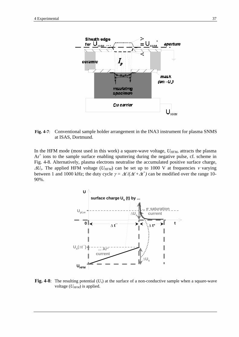
4 Experimental 37
In the HFM mode (most used in this work) a square-wave voltage, UHFM, attracts the plasma Ar+ ions to the sample surface enabling sputtering during the negative pulse, cf. scheme in Fig. 4-8. Alternatively, plasma electrons neutralise the accumulated positive surface charge,
Us. The applied HFM voltage (UHFM) can be set up to 1000 V at frequencies
varying between 1 and 1000 kHz; the duty cycle
= t-/( t-+ t+) can be modified over the range 10-90%.
Fig. 4-8: The resulting potential (Us) at the surface of a non-conductive sample when a square-wave voltage (UHFM) is applied.
Fig. 4-7: Conventional sample holder arrangement in the INA3 instrument for plasma SNMS at ISAS, Dortmund.
... e- saturationcurrentUs
Us( t¯ )
UHFM
Upl,w
surface charge Us (t) by ...
... Ar+
currentUs
t¯ t+
U
t0
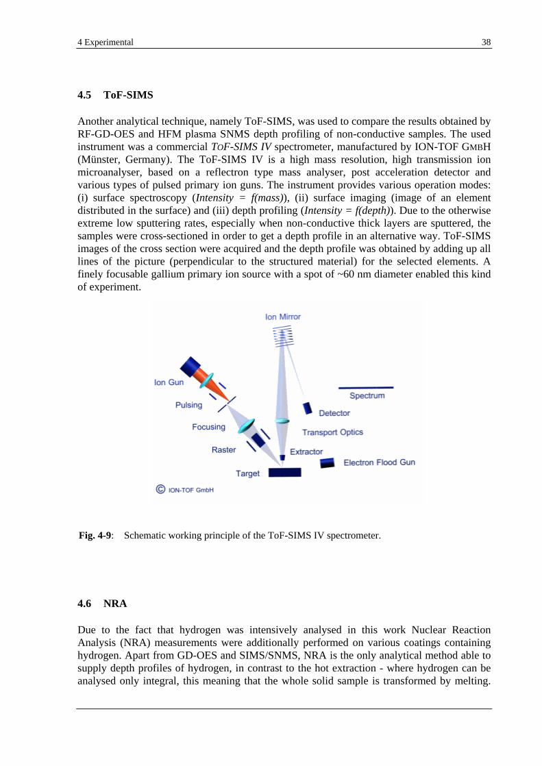
4 Experimental 38
4.5 ToF-SIMS
Another analytical technique, namely ToF-SIMS, was used to compare the results obtained by RF-GD-OES and HFM plasma SNMS depth profiling of non-conductive samples. The used instrument was a commercial TOF-SIMS IV spectrometer, manufactured by ION-TOF GMBH (Münster, Germany). The ToF-SIMS IV is a high mass resolution, high transmission ion microanalyser, based on a reflectron type mass analyser, post acceleration detector and various types of pulsed primary ion guns. The instrument provides various operation modes: (i) surface spectroscopy (Intensity = f(mass)), (ii) surface imaging (image of an element distributed in the surface) and (iii) depth profiling (Intensity = f(depth)). Due to the otherwise extreme low sputtering rates, especially when non-conductive thick layers are sputtered, the samples were cross-sectioned in order to get a depth profile in an alternative way. ToF-SIMS images of the cross section were acquired and the depth profile was obtained by adding up all lines of the picture (perpendicular to the structured material) for the selected elements. A finely focusable gallium primary ion source with a spot of ~60 nm diameter enabled this kind of experiment.
4.6 NRA
Due to the fact that hydrogen was intensively analysed in this work Nuclear Reaction Analysis (NRA) measurements were additionally performed on various coatings containing hydrogen. Apart from GD-OES and SIMS/SNMS, NRA is the only analytical method able to supply depth profiles of hydrogen, in contrast to the hot extraction - where hydrogen can be analysed only integral, this meaning that the whole solid sample is transformed by melting.
Fig. 4-9: Schematic working principle of the ToF-SIMS IV spectrometer.
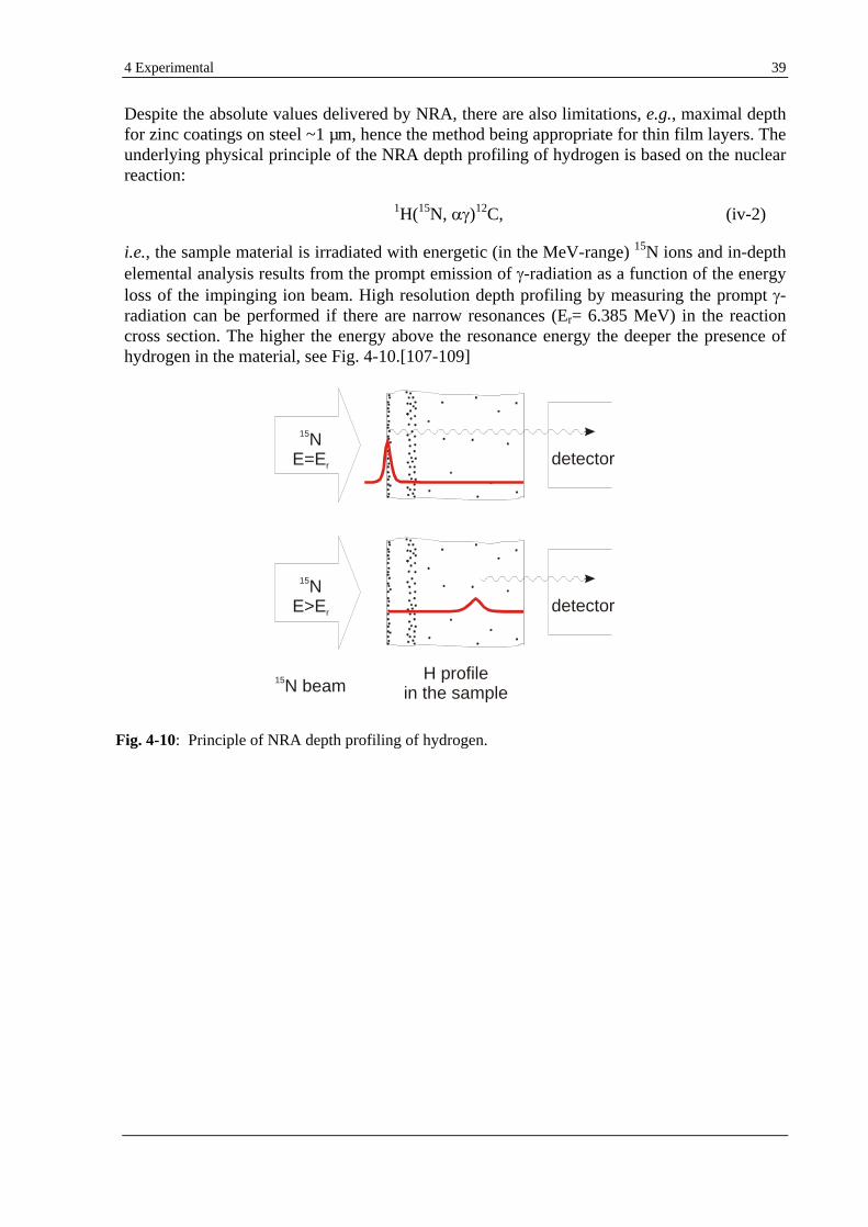
4 Experimental 39
Despite the absolute values delivered by NRA, there are also limitations, e.g., maximal depth for zinc coatings on steel ~1 µm, hence the method being appropriate for thin film layers. The underlying physical principle of the NRA depth profiling of hydrogen is based on the nuclear reaction:
1H(15N, )12C, (iv-2)
i.e., the sample material is irradiated with energetic (in the MeV-range) 15N ions and in-depth elemental analysis results from the prompt emission of -radiation as a function of the energy loss of the impinging ion beam. High resolution depth profiling by measuring the prompt -radiation can be performed if there are narrow resonances (Er= 6.385 MeV) in the reaction cross section. The higher the energy above the resonance energy the deeper the presence of hydrogen in the material, see Fig. 4-10.[107-109]
Fig. 4-10: Principle of NRA depth profiling of hydrogen.
detector
15NE>Er detector
15N beamH profile
in the sample
15NE=Er
5 Fundamental investigations 40
5 Fundamental investigations
As stated in OBJECTIVES, the present work is focussed on (i) the effect of hydrogen in GDS and (ii) on depth profiling of layered materials. Various applications in material science are shown in chapter 6. However, prerequisites in obtaining reliable analytical information from the GD-OES analysis are (i) a thorough insight in the complicate effect of hydrogen and (ii) methodical optimisation of depth profiling especially for electrically non-conductive thin layers. Section 5.1 is dedicated to fundamental experimental work on the hydrogen effect in GDS and Sec. 5.2 to the methodical optimisation of competitive depth profiling techniques, respectively.
5.1 Effect of hydrogen in GDS
Section 2.2 from PRE-CONSIDERATIONS has already highlighted the strong effect of contamination in GD-OES. As supposed by BENGTSON in his preliminary investigations on the hydrogen effect,[17] the causes for the various changes in the emission line intensities and sputtering rate reside in the "efficient" alteration of the excitation and ionisation mechanisms taking place in the pure noble gas plasma by the presence of hydrogen.
Since the hydrogen effect is individual for each analytical line of an element, the consideration of particular pure bulk materials is necessary for extensive investigations. It is expected that the energy change in elementary processes in the GD plasma containing hydrogen can contribute significantly to the occurrence of the hydrogen effect. Hence, energy level diagrams of the participating species, i.e., (i) sputtered material, (ii) carrier gas and (iii) hydrogen species (neutrals and ions), should constitute powerful tools in the attempt of looking for possible explanations.
5.1.1 Effect of hydrogen in an argon GD when copper is the sample
Pure bulk copper has been chosen as a sample to be investigated with respect to the hydrogen effect, due to its simple emission spectrum under the conditions used in the present work. There is also a plenty of data related to the copper emission spectrum in the GD-OES literature. Two different carrier noble gases have been considered, argon (Sec. 5.1.1), the conventional one, and neon (Sec. 5.1.2), as an alternative. The differing, e.g., ionisation potentials or excitation energies of the metastables for argon and neon should affect both the copper and hydrogen spectra in an individual manner. In each case, the emission spectrum of the carrier noble gas as well as of hydrogen has been thoroughly investigated, this being presented and discussed in separate subsections. Very recently, detailed calculations of the effect of hydrogen in low current GD sources of the VG9000 type have become available.[117] Whilst this information cannot be applied directly to the GRIMM source, the qualitative trends are relevant and will be quoted where relevant.
5 Fundamental investigations 41
Hydrogen is added into the GD source by mixing it in low concentrations with the carrier noble gas, i.e., as a molecular contamination. The mixing process is rigorously controlled by using of electronic gas flow devices (MFCs), the experimental procedure being detailed described in Sec. 4.3. Great attention was paid to the GD source cleanliness. Large pre-sputtering and stabilisation times of several minutes were able to supply accurate values for the measured line intensities.
The working conditions applied for this study of a large number of emission lines were: GD source diameter = 2.5 mm; constant voltage Vdc= 1000 V, constant (total) pressure 770 Pa (corresponding to 400 sccm), at increasing hydrogen relative partial pressures. The instrumentation used for individual spectral lines measurements was that at IFW DRESDEN, which through a separate channel is able to record an arbitrary emission line by the attached monochromator (as detailed described in Sec. 4.1). The following sections are intended to get an overview only on the changes in the emission spectra of an element, carrier gas and hydrogen. The changes in the dependent GD parameter (discharge current), the sputtering rate and sputtering crater shape are discussed in Sec. 5.1.7. At this stage, the working conditions were kept constant (Vdc= 1000 V and ptot
770 Pa); later in Sec. 5.1.9 they were varied for studies on some relevant analytical lines.
5.1.1.1 Atomic (Cu I) and ionic (Cu II) lines of copper
From the beginning on, one should note that the spectral lines emitted by excited neutral species are denoted with "I", and the spectral lines excited by single ionised energy levels are denoted with "II". In the present study only atomic and single ionised species are selectively considered, due to the huge volume of information still present even when copper is chosen as the sample. Also, because the monochromator used is of a low resolution (determined as being as low as ~0.05 nm for an entrance slit width of 50 µm,[31] only spectral lines which are intense and do not suffer from interference or self-absorption may be taken into account. In fact, in the case of argon as a carrier gas, all copper lines detected by the monochromator in IFW DRESDEN in the spectral range of ~220 770 nm under the selected conditions have been monitored, i.e., 19 atomic and 6 ionic emission lines of copper. The measured spectral lines are arranged in order of ascending excitation energy [118-120] in Table 5-1. The intensities of the selected emission lines from Table 5-1 were measured as a function of the hydrogen content (0 0.6% relative partial pressure) in the GD source and represented in Figs. 5-1a and b.
In order to get a more realistic insight in the changes caused by hydrogen on the spectral line intensities, the measured intensities of copper lines were divided by both the sputtering rate and the discharge current. Thus, the so-called "reduced intensity" is also shown in Figs. 5-1a and b. Note that detailed results on sputtering rate and discharge current are grouped in a separate section (Sec. 5.1.7). Only qualitatively at this point, for copper the discharge current - as the dependent GD parameter - as well as the sputtering rate decrease considerably at the addition of hydrogen into the GD source (Idc and SR, respectively, in Fig. 5-14, Sec. 5.1.7). And it is necessary to compensate for these changes. For a better view on the magnitude of the changes caused by hydrogen, the values of intensities and reduced intensities in pure argon were normalised to 1 (Figs. 5-1a and b). The same treatment is applied to the argon species, i.e., Ar I and Ar II (in Sec. 5.1.1.2).
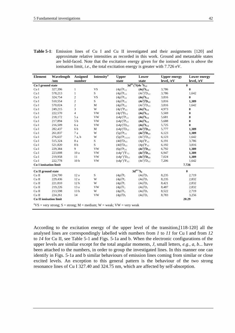
5 Fundamental investigations 42
Table 5-1: Emission lines of Cu I and Cu II investigated and their assignments [120] and
approximate relative intensities as recorded in this work. Ground and metastable states are bold-faced. Note that the excitation energy given for the ionised states is above the ionisation limit, i.e., the total excitation energy is greater with 7.726 eV.
Element Wavelength /nm
Assigned number
Intensitya Upper state
Lower state
Upper energy level, /eV
Lower energy level, /eV
Cu I ground state 3d10 (1S)4s 2S1/2 0 Cu I 327,396 1 VS (4p)2P1/2 (4s)2S1/2 3,786 0 Cu I 578,213 1 S (4p)2P1/2 (4s2)2D3/2 3,786 1,642 Cu I 324,754 2 VS (4p)2P3/2 (4s)2S1/2 3,816 0 Cu I 510,554 2 S (4p)2P3/2 (4s2)2D5/2 3,816 1,389 Cu I 570,024 2 M (4p)2P3/2 (4s2)2D3/2 3,816 1,642 Cu I 249,215 3 W (4p')4P3/2 (4s)2S1/2 4,973 0 Cu I 222,570 4 VW (4p')4D1/2 (4s)2S1/2 5,569 0 Cu I 218,172 5 a VW (s4p')2P1/2 (4s)2S1/2 5,681 0 Cu I 217,894 5 b VW (s4p')2P3/2 (4s)2S1/2 5,688 0 Cu I 216,509 6 a VW (s4p')2D3/2 (4s)2S1/2 5,725 0 Cu I 282,437 6 b M (s4p')2D5/2 (4s2)2D5/2 5,777 1,389 Cu I 261,837 7 a W (5p)2P3/2 (4s2)2D5/2 6,123 1,389 Cu I 276,637 7 a, b W (5p)2P1/2,3/2 (4s2)2D3/2 6,123 1,642 Cu I 515,324 8 a S (4d)2D3/2 (4p)2P1/2 6,191 3,786 Cu I 521,820 8 b S (4d)2D5/2 (4p)2P3/2 6,192 3,816 Cu I 229,384 9 VW (6p)2P3/2 (4s2)2D5/2 6,792 1,389 Cu I 223,008 10 a VW (s4p")2F7/2 (4s2)2D5/2 6,947 1,389 Cu I 219,958 11 VW (s4p")2D5/2 (4s2)2D5/2 7,024 1,389 Cu I 222,778 10 b VW (s4p")2F5/2 (4s2)2D3/2 7,206 1,642 Cu I ionisation limit 7.726
Cu II ground state 3d10 1S0 0 Cu II 224,700 12 a S (4p)3P2 (4s)3D3 8,235 2,719 Cu II 229,436 12 a W (4p)3P2 (4s)3D2 8,235 2,832 Cu II 221,810 12 b W (4p)3P1 (4s)3D2 8,421 2,832 Cu II 219,226 13 a VW (4p)3F3 (4s)3D2 8,487 2,832 Cu II 213,598 13 b W (4p)3F4 (4s)3D3 8,522 2,719 Cu II 224,261 14 VW (4p)3D3 (4s)1D2 8,783 3,256 Cu II ionisation limit 20.29 aVS = very strong; S = strong; M = medium; W = weak; VW = very weak
According to the excitation energy of the upper level of the transition,[118-120] all the analysed lines are correspondingly labelled with numbers from 1 to 11 for Cu I and from 12 to 14 for Cu II, see Table 5-1 and Figs. 5-1a and b. When the electronic configurations of the upper levels are similar except for the total angular moments, J, small letters, e.g., a, b... have been attached to the numbers, in order to group the investigated lines. In this manner one can identify in Figs. 5-1a and b similar behaviours of emission lines coming from similar or close excited levels. An exception to this general pattern is the behaviour of the two strong resonance lines of Cu I 327.40 and 324.75 nm, which are affected by self-absorption.
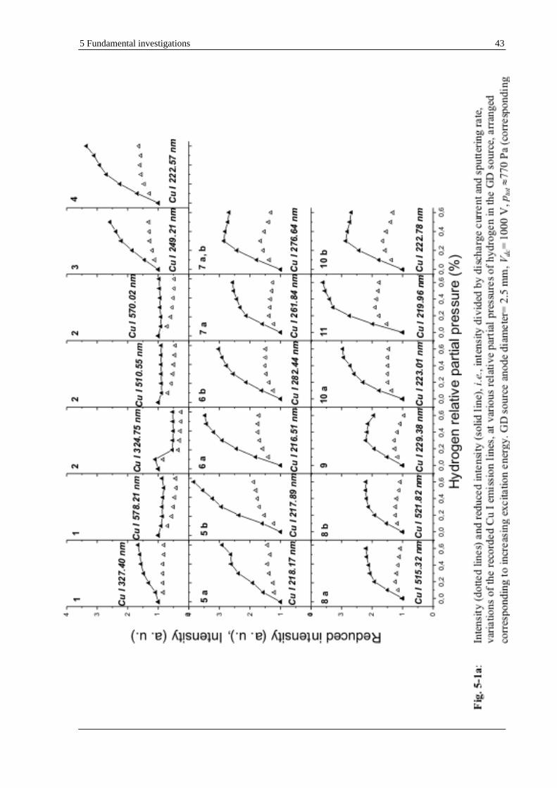
5 Fundamental investigations 43
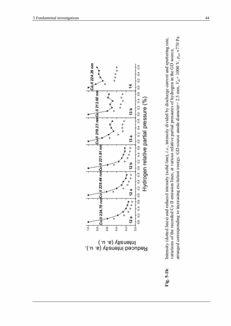
5 Fundamental investigations 44
5 Fundamental investigations 45
Some general trends are to be noticed in Figs. 5-1a and b:
i. The reduced intensity for most of the emission lines of Cu I (Fig. 5-1a) increases strongly with the addition of even small quantities of hydrogen (up to factor 4 for the line 217.89 nm, at 0.6% hydrogen relative partial pressure in the argon GD source). The 327.40 nm line of Cu I, used for the quantification of copper in many commercial available GD-OES spectrometers, is also considerably affected by hydrogen. Hence it could lead to a faulty quantification. Cu I 510.55 nm or Cu I 570.02 nm, both having reasonable intensities, could be better alternatives to it.
ii. A clear behaviour belongs to all the 6 lines of Cu II (see Fig. 5-1b) recorded here. These lines are emitted by energy levels grouped closely above the Cu II energy level at 8.23 eV, see Table 5-1. Due to (i) the magnitude of the hydrogen effect and (ii) its qualitative functional dependence on the excitation energy observed at the first sight already, a special attention is paid to this group of lines in the discussion from Sec. 5.1.1.4. The 219.23 nm Cu II line, used for quantification in many commercial GD-OES spectrometers, is strongly affected by the presence of hydrogen and consequently not appropriate for quantification without correction.
5.1.1.2 Atomic (Ar I) and ionic (Ar II) lines of argon
From the (line-rich) emission spectrum of argon, 19 atomic and 15 ionic lines have been selected to study the hydrogen influence. As for the copper case, the argon lines have been arranged in order of their excitation energy [118-120] and ordered in Table 5-2. The assigned numbers suggest again identical configurations up to the total angular momentum and the term of the upper levels.
The reduced intensities for the argon lines are calculated as measured intensities divided only by discharge current, see Figs. 5-2a and b. Note that the representation of the intensities and reduced intensities is similar that for the Cu I and II case in Figs. 5-1a and b, i.e., (i) normalised to 1 for the case in pure argon and (ii) scaled up to 1 for the Ar I lines, which decrease, and up to 4 for the Ar II lines, which increase slightly. From Figs. 5-2a and b it can be easily observed that for the investigated Ar I as well as for Ar II lines there are also general trends to be seen at increasing hydrogen partial pressures:
(i) The reduced intensities of the Ar I lines decrease exponentially-like, e.g., down to ~30% for the 549.59 nm line, eventually followed by a plateau or even enhancements (for lines having lower excitation energy). The higher the excitation energy, the more pronounced is the decrease. The Ar I emission line at 415.86 nm selected for analysis using commercial instruments suffers also a decrease of intensity down to ~60% at least, at ~0.3% hydrogen in the GD source.
(ii) Contrary to the expectations, most of the Ar II lines investigated here and having quite high excitation energies, i.e., ~18-23 eV over the ionisation limit of argon (15.76 eV), show a more or less pronounced increase of the reduced intensity: for lower excitation energies saturation or light decrease are characteristic with increasing hydrogen content; the higher the excitation energy, the more evident is an increase.
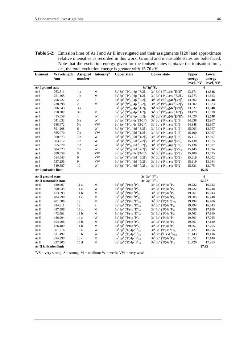
5 Fundamental investigations 46
Table 5-2: Emission lines of Ar I and Ar II investigated and their assignments [120] and approximate
relative intensities as recorded in this work. Ground and metastable states are bold-faced. Note that the excitation energy given for the ionised states is above the ionisation limit, i.e., the total excitation energy is greater with 15.76 eV.
Element Wavelength /nm
Assigned
number Intensitya Upper state Lower state Upper
energy level, /eV
Lower energy level, /eV
Ar I ground state 3s2 3p6 1S0 0 Ar I 763,511 1 a M 3s2 3p5 (2P0
3/2)4p 2[3/2]2 3s2 3p5 (2P03/2)4s 2[3/2]0
2 13,171 11,548 Ar I 751,465 1 b M 3s2 3p5 (2P0
3/2)4p 2[1/2]0 3s2 3p5 (2P03/2)4s 2[3/2]0
1 13,273 11,623 Ar I 706,722 2 S 3s2 3p5 (2P0
1/2)4p 2[3/2]2 3s2 3p5 (2P03/2)4s 2[3/2]0
2 13,302 11,548 Ar I 738,398 2 M 3s2 3p5 (2P0
1/2)4p 2[3/2]2 3s2 3p5 (2P03/2)4s 2[3/2]0
1 13,302 11,623 Ar I 696,543 3 a S 3s2 3p5 (2P0
1/2)4p 2[1/2]1 3s2 3p5 (2P03/2)4s 2[3/2]0
2 13,327 11,548 Ar I 750,387 3 b M 3s2 3p5 (2P0
1/2)4p 2[1/2]0 3s2 3p5 (2P01/2)4s 2[1/2]0
1 13,479 11,828 Ar I 415,859 4 W 3s2 3p5 (2P0
3/2)5p 2[3/2]2 3s2 3p5 (2P03/2)4s 2[3/2]0
2 14,528 11,548 Ar I 641,632 5 a W 3s2 3p5 (2P0
3/2)6s 2[3/2]02 3s2 3p5 (2P0
3/2)4p 2[1/2]1 14,838 12,907 Ar I 638,472 5 b VW 3s2 3p5 (2P0
3/2)6s 2[3/2]01 3s2 3p5 (2P0
3/2)4p 2[1/2]1 14,848 12,907 Ar I 591,208 6 W 3s2 3p5 (2P0
1/2)4d 2[3/2]01 3s2 3p5 (2P0
3/2)4p 2[1/2]1 15,003 12,907 Ar I 565,070 7 a VW 3s2 3p5 (2P0
3/2)5d 2[1/2]00 3s2 3p5 (2P0
3/2)4p 2[1/2]1 15,100 12,907 Ar I 560,673 7 b W 3s2 3p5 (2P0
3/2)5d 2[1/2]01 3s2 3p5 (2P0
3/2)4p 2[1/2]1 15,117 12,907 Ar I 603,212 7 c W 3s2 3p5 (2P0
3/2)5d 2[7/2]04 3s2 3p5 (2P0
3/2)4p 2[5/2]3 15,130 13,075 Ar I 555,870 7 d W 3s2 3p5 (2P0
3/2)5d 2[3/2]02 3s2 3p5 (2P0
3/2)4p 2[1/2]1 15,136 12,907 Ar I 604,323 7 e W 3s2 3p5 (2P0
3/2)5d 2[7/2]03 3s2 3p5 (2P0
3/2)4p 2[5/2]2 15,145 13,094 Ar I 588,859 8 VW 3s2 3p5 (2P0
3/2)7s 2[3/2]02 3s2 3p5 (2P0
3/2)4p 2[5/2]3 15,180 13,075 Ar I 614,543 9 VW 3s2 3p5 (2P0
1/2)5d 2[5/2]03 3s2 3p5 (2P0
1/2)4p 2[3/2]2 15,319 13,302 Ar I 557,255 9 VW 3s2 3p5 (2P0
1/2)5d 2[5/2]03 3s2 3p5 (2P0
3/2)4p 2[5/2]2 15,319 13,094 Ar I 549,587 10 W 3s2 3p5 (2P0
3/2)6d 2[7/2]04 3s2 3p5 (2P0
3/2)4p 2[5/2]3 15,331 13,075 Ar I ionisation limit 15.76
Ar II ground state 3s2 3p5 2P03/2 0
Ar II metastable state 3s2 3p5 2P01/2 0.177
Ar II 480,607 11 a M 3s2 3p4 (3P)4p 4P05/2 3s2 3p4 (3P)4s 4P5/2 19,222 16,643
Ar II 500,935 11 a W 3s2 3p4 (3P)4p 4P05/2 3s2 3p4 (3P)4s 4P3/2 19,222 16,748
Ar II 473,593 11 b M 3s2 3p4 (3P)4p 4P03/2 3s2 3p4 (3P)4s 4P5/2 19,261 16,643
Ar II 484,790 11 c M 3s2 3p4 (3P)4p 4P01/2 3s2 3p4 (3P)4s 4P3/2 19,305 16,748
Ar II 401,386 12 M 3s2 3p4 (3P)4p 4D07/2 3s2 3p4 (3P)3d 4D7/2 19,494 16,406
Ar II 434,811 12 S 3s2 3p4 (3P)4p 4D07/2 3s2 3p4 (3P)4s 4P5/2 19,494 16,643
Ar II 487,986 13 a M 3s2 3p4 (3P)4p 2D05/2 3s2 3p4 (3P)4s 2P3/2 19,680 17,140
Ar II 472,691 13 b M 3s2 3p4 (3P)4p 2D03/2 3s2 3p4 (3P)4s 2P3/2 19,762 17,140
Ar II 488,904 14 a W 3s2 3p4 (3P)4p 2P01/2 3s2 3p4 (3P)4s 2P1/2 19,801 17,265
Ar II 454,508 14 b M 3s2 3p4 (3P)4p 2P03/2 3s2 3p4 (3P)4s 2P3/2 19,867 17,140
Ar II 476,489 14 b M 3s2 3p4 (3P)4p 2P03/2 3s2 3p4 (3P)4s 2P1/2 19,867 17,265
Ar II 501,716 15 a W 3s2 3p4 (1D)4p 2F05/2 3s2 3p4 (3P)3d 2D3/2 21,127 18,656
Ar II 611,492 15 b W 3s2 3p4 (1D)4p 2F07/2 3s2 3p4 (1D)3d 2G9/2 21,143 19,116
Ar II 294,290 15 c M 3s2 3p4 (1D)4p 2P03/2 3s2 3p4 (3P)4s 2P3/2 21,351 17,140
Ar II 297,905 15 d M 3s2 3p4 (1D)4p 2P01/2 3s2 3p4 (3P)4s 2P1/2 21,426 17,265
Ar II ionisation limit 27.63 aVS = very strong; S = strong; M = medium; W = weak; VW = very weak
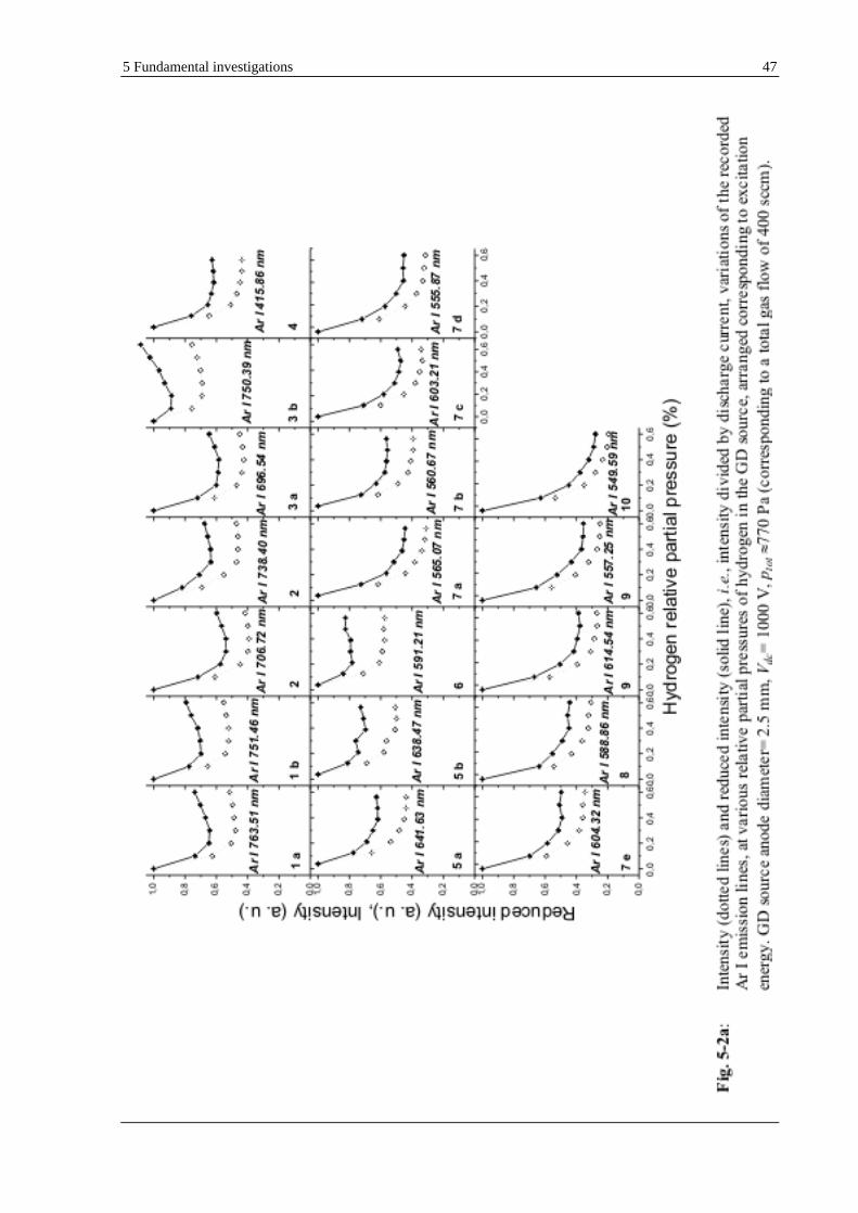
5 Fundamental investigations 47
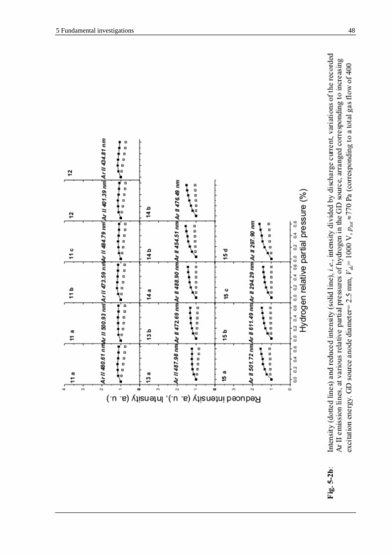
5 Fundamental investigations 48
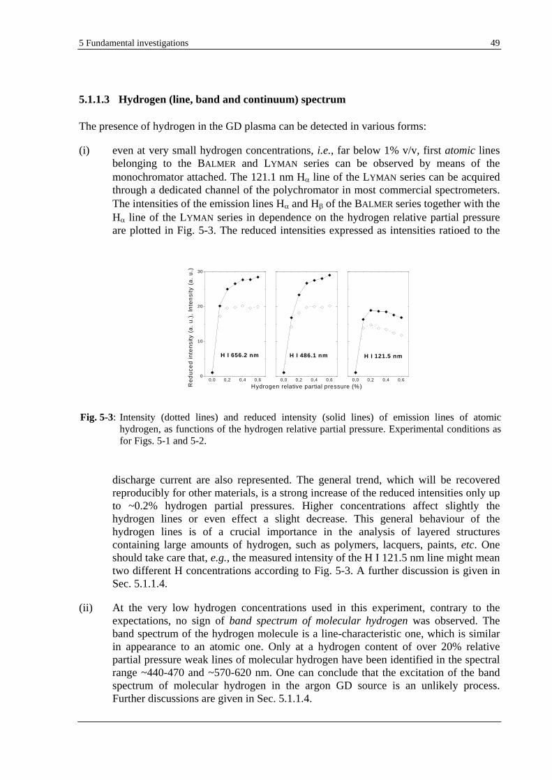
5 Fundamental investigations 49
5.1.1.3 Hydrogen (line, band and continuum) spectrum
The presence of hydrogen in the GD plasma can be detected in various forms:
(i) even at very small hydrogen concentrations, i.e., far below 1% v/v, first atomic lines belonging to the BALMER and LYMAN series can be observed by means of the monochromator attached. The 121.1 nm H
line of the LYMAN series can be acquired through a dedicated channel of the polychromator in most commercial spectrometers. The intensities of the emission lines H and H of the BALMER series together with the H
line of the LYMAN series in dependence on the hydrogen relative partial pressure are plotted in Fig. 5-3. The reduced intensities expressed as intensities ratioed to the
discharge current are also represented. The general trend, which will be recovered reproducibly for other materials, is a strong increase of the reduced intensities only up to ~0.2% hydrogen partial pressures. Higher concentrations affect slightly the hydrogen lines or even effect a slight decrease. This general behaviour of the hydrogen lines is of a crucial importance in the analysis of layered structures containing large amounts of hydrogen, such as polymers, lacquers, paints, etc. One should take care that, e.g., the measured intensity of the H I 121.5 nm line might mean two different H concentrations according to Fig. 5-3. A further discussion is given in Sec. 5.1.1.4.
(ii) At the very low hydrogen concentrations used in this experiment, contrary to the expectations, no sign of band spectrum of molecular hydrogen was observed. The band spectrum of the hydrogen molecule is a line-characteristic one, which is similar in appearance to an atomic one. Only at a hydrogen content of over 20% relative partial pressure weak lines of molecular hydrogen have been identified in the spectral range ~440-470 and ~570-620 nm. One can conclude that the excitation of the band spectrum of molecular hydrogen in the argon GD source is an unlikely process. Further discussions are given in Sec. 5.1.1.4.
Fig. 5-3: Intensity (dotted lines) and reduced intensity (solid lines) of emission lines of atomic hydrogen, as functions of the hydrogen relative partial pressure. Experimental conditions as for Figs. 5-1 and 5-2.
0,0 0,2 0,4 0,60
10
20
30
Re
du
ced
inte
nsi
ty (
a.
u.)
, In
ten
sity
(a
. u
.)
H I 656.2 nm
0,0 0,2 0,4 0,6
Hydrogen relative partial pressure (%)
H I 486.1 nm
0,0 0,2 0,4 0,6
H I 121.5 nm
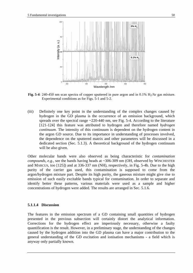
5 Fundamental investigations 50
(iii) Definitely one key point in the understanding of the complex changes caused by hydrogen in the GD plasma is the occurrence of an emission background, which spreads over the spectral range ~220-440 nm, see Fig. 5-4. According to the literature [121-124] this feature was attributed to hydrogen and therefore named hydrogen continuum. The intensity of this continuum is dependent on the hydrogen content in the argon GD source. Due to its importance in understanding of processes involved, the dependence on the sputtered matrix and other parameters will be discussed in a dedicated section (Sec. 5.1.3). A theoretical background of the hydrogen continuum will be also given.
Other molecular bands were also observed as being characteristic for contamination compounds, e.g., see the bands having heads at ~306-309 nm (OH, observed by WINCHESTER
and MARCUS, too [125]) and at 336-337 nm (NH), respectively, in Fig. 5-4b. Due to the high purity of the carrier gas used, this contamination is supposed to come from the argon/hydrogen mixture part. Despite its high purity, the gaseous mixture might give rise to emission of such easily excitable bands typical for contamination. In order to separate and identify better these patterns, various materials were used as a sample and higher concentrations of hydrogen were added. The results are arranged in Sec. 5.1.6.
5.1.1.4 Discussion
The features in the emission spectrum of a GD containing small quantities of hydrogen presented in the previous subsection will certainly distort the analytical information. Corrections for the hydrogen effect are imperiously necessary, otherwise a faulty quantification is the result. However, in a preliminary stage, the understanding of the changes caused by the hydrogen addition into the GD plasma can have a major contribution to the general understanding of the GD excitation and ionisation mechanisms - a field which is anyway only partially known.
Fig. 5-4: 240-450 nm scan spectra of copper sputtered in pure argon and in 0.1% H2/Ar gas mixture. Experimental conditions as for Figs. 5-1 and 5-2.
250 300 350 400 4500
50
100
0.1% H2
Wavelength /nm
0
50
100
0% H2
Inte
nsity
(a. u
.)
5 Fundamental investigations 51
In order to get an overview on the large number of investigated emission lines of copper, argon and hydrogen presented in the previous subsections, the energy levels responsible for the corresponding transitions are schematically presented in energy level diagrams. Hence, Fig. 5-5 puts together partial energy diagrams of copper (Cu I and Cu II), argon (Ar I and Ar II) and the hydrogen molecule. From this picture, some elementary processes become evident:
The emission lines mostly affected by hydrogen are those belonging to the Cu II lines group excited at 8.23-8.78 eV above the ionisation potential and presented in Fig. 5-1b. It has been demonstrated by STEERS and FIELDING,[28] that the Cu II 224.7 nm and 229.44 nm lines (same upper state, 8.23 + 7.73 eV) are excited by an asymmetric charge transfer (CT) process from a metastable state, Ar II 2P1/2, 0.18 eV above the Ar II 2P3/2 ground state (15.76 eV):
?E
Cu Ar Cu Ar ,*g0,CTg0,m, , (v-1)
where the symbols 0, +, g, *, and m indicate neutral, single ionised, ground, excited, and metastable states, respectively. E in this case is 0.20 eV. Furthermore, for the next Cu II levels above the 8.23 eV, for which E becomes negative, it was shown by ROZSA et al. [126, 127] that when the argon ions have sufficient kinetic energy, CT is still possible. This sustains the experiments of STEERS and FIELDING.[28] According to them, the Cu II lines intensity in argon relative to those in helium (where no selective excitation is possible) decreases exponentially with ascending excitation energy above the 8.23 eV. In other words, the lower the energy matching is (i.e., the bigger the energy gap), the less efficient the CT process. Note that if krypton is used as the plasma gas, so that no CT excitation is possible (as in helium), all this group of lines have similar intensities.[29] Looking at the gradual changes of the Cu II lines from Fig. 5-1b, it becomes obviously that the addition of hydrogen to argon causes an effective quenching of the CT process (see Fig. 5-5).[128-130]
Further on, following the reasons of the quenching of the Cu II line intensities, one can conclude that, the Ar II 2P1/2 metastables as well as very likely the Ar II 2P3/2 ground state ions, in turn are strongly depopulated by hydrogen. Two comments may be helpful at this point: (i) This last assumption is in accord, at least partially, with the decrease of the discharge current, when it is the dependent GD parameter (point suggested in [131], too), see, e.g., Sec. 5.1.7; (ii) GD-MS measurements of copper in argon having added hydrogen show a drop in the intensity of argon single ionised (see Sec. 5.1.4). Hence, both evidence make realistic the assumption on the depopulation of the Ar II 2P3/2 ground state by hydrogen.
On the other hand, a very clear "block" behaviour, namely decrease, is shown by the Ar I lines presented in Fig. 5-2a. Moreover, the higher the excitation energy of the Ar I lines (and hence the closer the excitation energy to the Ar I ionisation limit), the more similar is the quenching of the Ar I lines intensities to that of the Cu II line intensities reported above. Hence, it seems that, for both quenching processes (i) of the Ar II 2P3/2 ground state and the Ar II 2P1/2 metastables and (ii) the Ar I states there is the same reason. If the following assumption, that part of the excitation of the of Ar I lines and the production of ground state Ar II is due to a two-step process via the metastable states,[132, 133] then one can further assume that hydrogen quenches efficiently the Ar I metastables at 11.55 and 11.72 eV (see Table 5-2).
At this point one should refer to the appearance of the hydrogen continuum, which by the understanding of its emission process can offer more linking information. Details are given in Sec. 5.1.3. Nevertheless, Fig. 5-5 already shows that one possible excitation of the hydrogen
5 Fundamental investigations 52
continuum can be by collisions of the hydrogen molecules in the ground state with the Ar I metastables having the excitation energies of 11.55 and 11.72 eV, respectively, i.e., by a Penning excitation (PE) process. Section 5.1.3 will also clarify that a possible competitive process of excitation of the hydrogen continuum by electron impact is very unlikely. For this, an alternative noble carrier gas, having its metastables at other energies, was used at the same GD parameters.
Hence, one can draw the conclusion that hydrogen quenches directly (by PE) (i) the Ar I metastable states, which in turn causes further (ii) the quenching of the production of the Ar I excited states and Ar II ground states, and further on (iii) of the Cu II excited states reported above. The whole process can be easily followed in Fig. 5-5.
Taking into account now the behaviour of the Ar II line intensities when hydrogen is present in an argon GD plasma (see Fig. 5-2a), surprisingly, it seems that they are not considerably affected by the presence of hydrogen. However, there are evidence [132, 133] that the excitation of the high energy transitions of Ar II is most probably due to electron impact of the argon atom ground state, i.e., a one-step electron impact process. This means that this latter process would not be directly affected by the quenching of the metastable Ar I states. BOGAERTS [117] has recently also shown that for a GD-MS cell at any rate, the addition of hydrogen to the argon does not alter the electron energy distribution function (EEDF). A similar figure could likely be extended for the GD plasma in the conditions used in this work, too. Hence, in spite of the slight changes in the Ar II line intensities measured here, the total Ar II density decreases as a result of the presence of hydrogen in an argon GD plasma. This will be confirmed by GD-MS measurements (Sec. 5.1.4) and of the decrease of the current as the dependent GD parameter. On the other hand, hydrogen molecules can be ionised by CT by the argon metastable ions (see Fig. 5-5). If the Ar metastables are quenched by hydrogen, a supplementary decrease of the density of the hydrogen molecular ions may follow.
The Cu I lines shown in Fig. 5-1a, being emitted by energy levels having very low excitation energies, are at the first sight subject to arbitrary increases or decreases of their intensities at the hydrogen addition. Enhancements of the intensities of Cu I lines could be assumed as coming from de-excitations of copper states having higher excitation energies. As one can see in the next sections, the general trend of the change in the emission spectra at the hydrogen addition is a decrease.
Fourier Transform Spectroscopy (FTS) measurements performed by STEERS [133] on the 811.5 nm Ar I line have been performed in order to get direct information on the Ar I metastables. The lower level of the appropriate transition is one of the two metastables of Ar I at 11.55 eV and the upper state has a 13.08 eV excitation energy, see Fig. 5-5. Two situations were investigated: pure argon and hydrogen/argon mixture. In the first case the high-resolved line profile shows a clear self-reversal. The occurrence of self-absorption is attributed to the absorption of the light quanta emitted in the GD part near to the sputtered sample by the same species (involving the same energy transition, but in the inverse way) in the cold part of the GD, i.e., by the non-emitting population near the edge of the GD between GD and detection system.[134, 135] If the self-absorption is severe enough, a minimum in the centre of the line profile, i.e., a self-reversal, can be observed. In the case when hydrogen is added to the
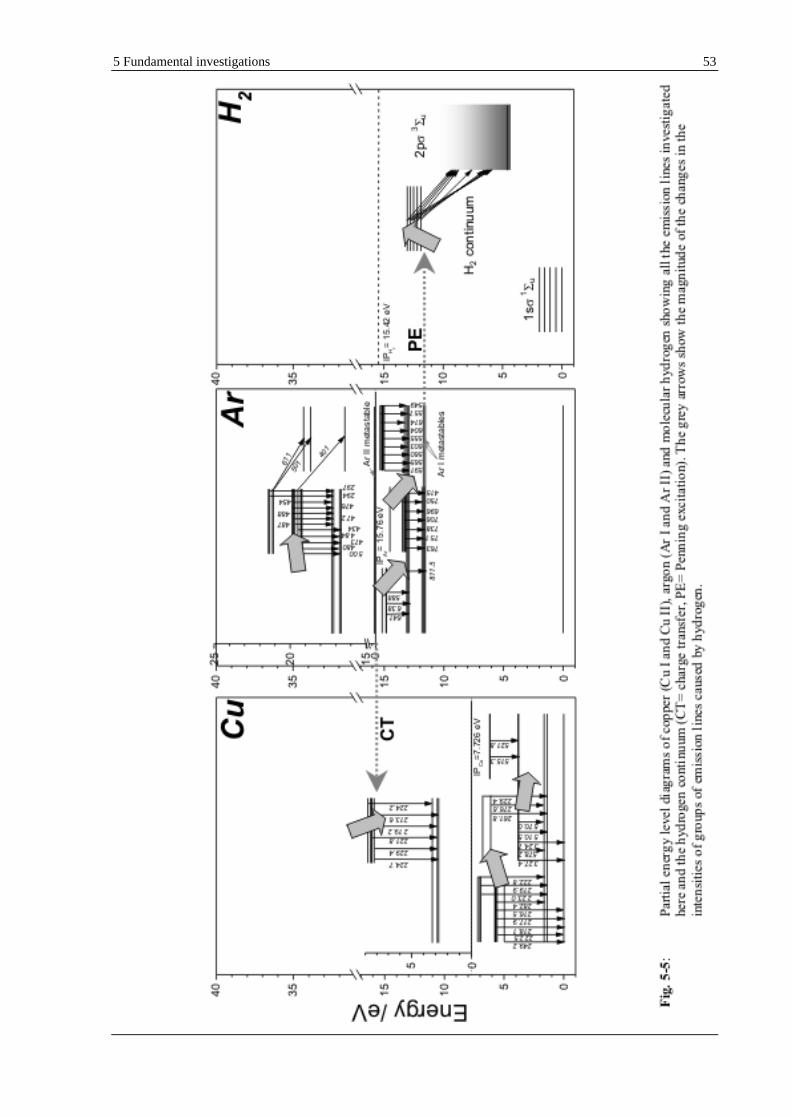
5 Fundamental investigations 53
5 Fundamental investigations 54
argon GD, no self-absorption is present. Thus, this confirms that the presence of hydrogen in the GD causes a depopulation of the Ar I metastables in the cold part of the GD.
Some comments on the occurrence of the hydrogen spectrum (Sec. 5.1.1.3) are also necessary.
A very similar behaviour of the H I 121.5 nm line will be re-found for different configurations of the GD source and for other materials, too. It is interesting to relate these data to the values from the experiments of WILKEN et al.,[32] who have found for hydrogen as an analyte in powder pellets (various concentrations of TiH2 mixed with copper) nearly linear calibration curves up to a maximal concentration corresponding to 100% TiH2. This dependence is in agreement with the hydrogen curves shown in Fig. 5-3 if one takes into account the dissolution of the analytes in the GD plasma of a factor of ~103. In other words, the WILKEN's curves for hydrogen contained in pellets are "hidden" in the sharp rise of the curves in Fig. 5-3 in the low range of concentration up to ~0.2 % hydrogen.
On the other hand, BOGAERTS and GIJBELS [136] have predicted the dissociation degree for the hydrogen molecules in a GD-OES source. Their estimate based on simple balance equations was of ~67% under typical GD-OES conditions (GRIMM type GD source) and ~5% for a low current GD-MS cell. However, more accurate modelling calculations, just published,[117] have shown that the original GD-MS figure was a considerable over-estimate (several orders of magnitude). Moreover, the dissociation degree was found as decreasing exponentially-like with increasing hydrogen concentration. Even at these different conditions, the new predicted results of BOGAERTS [117] must be definitely considered at further investigations. E.g., the behaviour of the predicted atomic hydrogen density with the (molecular) hydrogen added into the argon GD plasma looks qualitatively very similar to those of the hydrogen atomic lines measured in this work (and shown in Fig. 5-3).
In order to find more experimental evidence which could support the suggestions above, next sections deepen further the investigations on the understanding of the hydrogen effect.
5.1.2 Effect of hydrogen in a neon GD when copper is the sample
It should be noted that this subsection is intended to have the similar structure as the previous one (Sec. 5.1.1), with use of neon as the noble carrier gas instead of argon. The same samples of bulk copper were used. However, due to the large volume of information only the most relevant features are selected for presentation here. For more details, see [137].
5.1.2.1 Emission lines of copper (Cu I and II), neon (Ne I and II) and hydrogen
The same instrumentation and the same GD parameters were used as in the previous section in order to compare better the two situations. Due to the higher ionisation potential of neon it is necessary to increase considerably the total pressure in order to get the same GD power as in the argon case. Hence, at the voltage of Vdc= 1000 V a total gas flow (including the Ne/H flow line) of 1200 sccm - corresponding to a GD pressure of ~2310 Pa - was necessary.
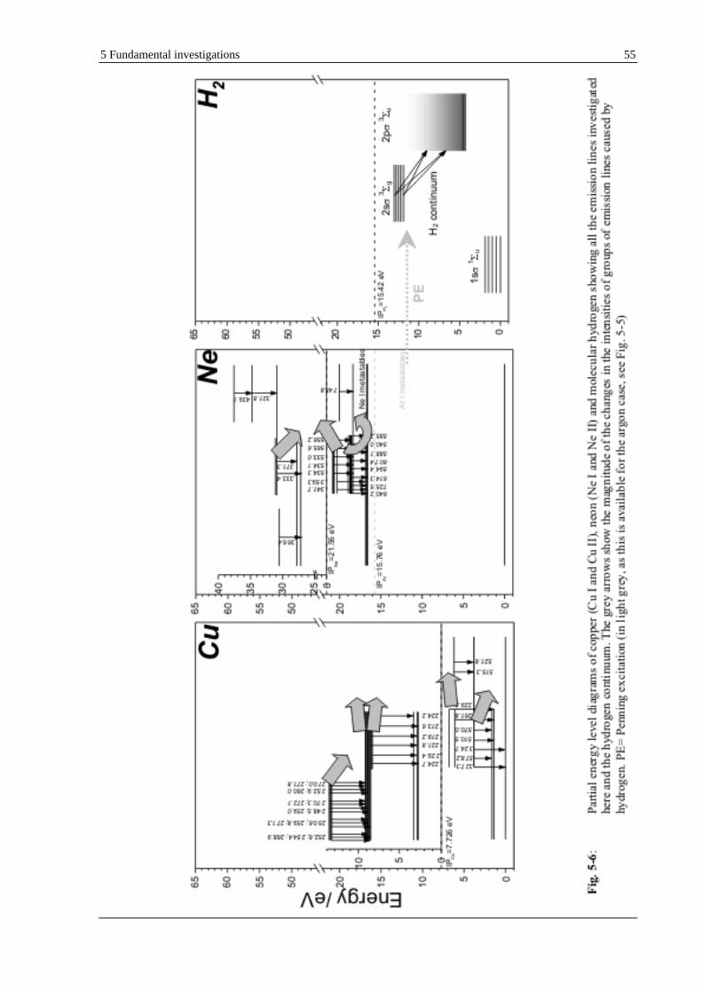
5 Fundamental investigations 55
5 Fundamental investigations 56
All the emission lines of Cu I and II and Ne I and II monitored are represented together with a partial diagram of the hydrogen molecule in Fig. 5-6. The general trends of particular species are semi-quantitatively expressed by arrows in the same figure:
(i) Those Cu I lines excited by very low energies (3.79 and 3.82 eV) decrease considerably under the presence of small quantities of hydrogen in the neon plasma. Contrary, Cu I lines excited at energies close above 6 eV remain unchanged or increase slightly.
(ii) The Cu II lines could also be classified in two groups of different trends. The lines coming from the 8.23-8.78 eV levels (the same group as in the argon GD case) vary this time just a little. A group of relatively intense Cu II lines, not observed in the case of argon at all, and identified as being emitted from levels having higher energies of ~13-14 eV, CT excited by neon ions,[28, 133] clearly decrease.
(iii) The intensities of some Ne I lines increase monotonically, others (at lower energies excited) increase only after an initial fall.
(iv) Considerable decreases are observed in the behaviour of the Ne II line intensities.
As far as the hydrogen spectrum is concerned, the intensity variations of the atomic lines of hydrogen look very similar to those in the argon case. However, high resolution FTS measurements [133] have shown that with neon, the hydrogen lines H I 486.1 nm and H I 656.2 nm have a clear DOPPLER (GAUSSIAN) profile. With argon the lower part of the profile is dramatically broadened with a shape characteristic of collisional interactions. The band spectrum of molecular hydrogen is also not visible at all at these small concentrations of hydrogen. The crucial difference lies in the absence of the hydrogen continuum in the case of using neon.
5.1.2.2 Discussion and comparison with the argon case
As already stated above, the use of neon as a noble gas is treated not as largely as in the corresponding section when argon is used. Not only the complexity of the mechanisms changed by hydrogen, but also the fact that neon is more expensive and supplementary necessary in enhanced quantities make neon not so attractive for routine GD-OES analysis.
However, its use in this study is worthwhile at least for the clarification of the excitation of the hydrogen continuum. The fact that the hydrogen continuum does not appear any more if neon is the carrier gas sustains the suggestion in the previous sub-section (Sec. 5.1.1.4), that the excitation of the hydrogen continuum in argon is done by PE with the argon metastables of 11.55 and 11.72 eV. The metastables of neon, being situated at significant higher energies, i.e., 16.62 and 16.72 eV, are not able to excite the hydrogen molecular state 2s
3g, see Fig.
5-6 (for comparison, the argon metastables are shown in grey). Secondary changes such as the quenching of the intensities of the Cu II line group at 8.23-8.78 eV by hydrogen in argon remain then to be attributed to the quenching of the argon metastables.
Similar to the argon metastables, the neon metastables are able to ionise (by PI) the hydrogen molecules (IPH2= 15.42 eV). However, because the neon metastables are not quenched by hydrogen, PI can compensate for any loss of neon ions.[133] This might constitute the reason
5 Fundamental investigations 57
of the slight change of the current when hydrogen is added to a neon GD (see, e.g., Fig. 5-14b in Sec. 5.1.7).
With other words, it is clear now that, the "unhappy" energy match of the atomic metastables of the conventionally used carrier gas argon and the molecular hydrogen state exciting the hydrogen continuum emphasises the decisive role of the metastables in a GD. It should be noted that this PE process was not predicted in the GD literature [136] as being so efficient. The next section (Sec. 5.1.3) evidences the features of this hydrogen continuum by various experiments.
5.1.3 Hydrogen continuum
In Fig. 5-4 one could already see the hydrogen continuum at 0.1% hydrogen in argon in the case of copper as a sputtered material. In order to investigate better the characteristics of the hydrogen continuum, higher concentrations of hydrogen were deliberately added to the plasma gas. Various pure bulk materials and again neon, as an alternative carrier gas, were used. The experimental results are presented in Sec. 5.1.3.1 and the theory of the hydrogen continuum in Sec. 5.1.3.2.
5.1.3.1 Experimental investigations
Fig. 5-7 shows an overview on various experimental conditions resulting in the appearance of the hydrogen continuum. In the left column argon is the carrier gas, and in the right one neon, respectively. Three representative bulk samples were used: copper, stainless steel and titanium; a block of four scan spectra belongs to each of them. The second row of each block are scan spectra emitted when argon and neon, respectively, are mixed with a defined fraction of hydrogen (2% v/v).
A very clear continuum can be observed in the case of argon containing hydrogen. Moreover, under similar conditions the features of this continuum are independent of the sample. On the other hand, no sign of an emission background is visible in the case of using neon. Note that both iron and titanium emit very dense line emission spectra, which can therefore be misinterpreted as a continuum.
The lower wavelength sensitivity of the spectrograph (and of the monochromator used, too) ends at about 200 nm. Therefore, no statement about the behaviour of the background below this wavelength is possible from this experiments. The explanations given in the next section (Sec. 5.1.3.2) will suggest that this continuos background also exists below 200 nm.
One can also see in Fig. 5-7 that the general trend of the changes in the emission lines of the spectra emitted in argon is a decrease. The signal given by the total light emitted was not recorded, however, it is very likely that it decreases by adding hydrogen to argon, in the same
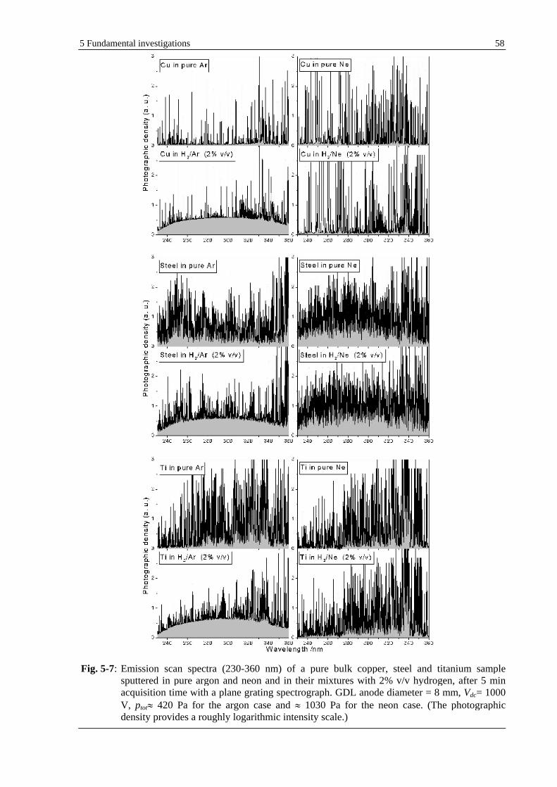
5 Fundamental investigations 58
Fig. 5-7: Emission scan spectra (230-360 nm) of a pure bulk copper, steel and titanium sample sputtered in pure argon and neon and in their mixtures with 2% v/v hydrogen, after 5 min acquisition time with a plane grating spectrograph. GDL anode diameter = 8 mm, Vdc= 1000 V, ptot
420 Pa for the argon case and
1030 Pa for the neon case. (The photographic density provides a roughly logarithmic intensity scale.)
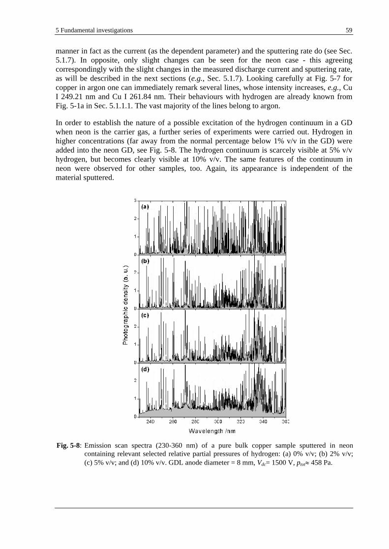
5 Fundamental investigations 59
manner in fact as the current (as the dependent parameter) and the sputtering rate do (see Sec. 5.1.7). In opposite, only slight changes can be seen for the neon case - this agreeing correspondingly with the slight changes in the measured discharge current and sputtering rate, as will be described in the next sections (e.g., Sec. 5.1.7). Looking carefully at Fig. 5-7 for copper in argon one can immediately remark several lines, whose intensity increases, e.g., Cu I 249.21 nm and Cu I 261.84 nm. Their behaviours with hydrogen are already known from Fig. 5-1a in Sec. 5.1.1.1. The vast majority of the lines belong to argon.
In order to establish the nature of a possible excitation of the hydrogen continuum in a GD when neon is the carrier gas, a further series of experiments were carried out. Hydrogen in higher concentrations (far away from the normal percentage below 1% v/v in the GD) were added into the neon GD, see Fig. 5-8. The hydrogen continuum is scarcely visible at 5% v/v hydrogen, but becomes clearly visible at 10% v/v. The same features of the continuum in neon were observed for other samples, too. Again, its appearance is independent of the material sputtered.
Fig. 5-8: Emission scan spectra (230-360 nm) of a pure bulk copper sample sputtered in neon containing relevant selected relative partial pressures of hydrogen: (a) 0% v/v; (b) 2% v/v; (c) 5% v/v; and (d) 10% v/v. GDL anode diameter = 8 mm, Vdc= 1500 V, ptot 458 Pa.
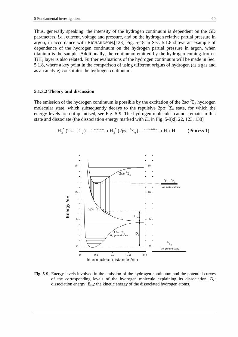
5 Fundamental investigations 60
Thus, generally speaking, the intensity of the hydrogen continuum is dependent on the GD parameters, i.e., current, voltage and pressure, and on the hydrogen relative partial pressure in argon, in accordance with RICHARDSON.[123] Fig. 5-18 in Sec. 5.1.8 shows an example of dependence of the hydrogen continuum on the hydrogen partial pressure in argon, when titanium is the sample. Additionally, the continuum emitted by the hydrogen coming from a TiH2 layer is also related. Further evaluations of the hydrogen continuum will be made in Sec. 5.1.8, where a key point in the comparison of using different origins of hydrogen (as a gas and as an analyte) constitutes the hydrogen continuum.
5.1.3.2 Theory and discussion
The emission of the hydrogen continuum is possible by the excitation of the 2s 3g hydrogen
molecular state, which subsequently decays to the repulsive 2p
3u state, for which the
energy levels are not quantised, see Fig. 5-9. The hydrogen molecules cannot remain in this state and dissociate (the dissociation energy marked with De in Fig. 5-9):[122, 123, 138]
H H ) 2ps( H ) (2ss
H ondissociatiu
3*2
continuum3*2 g (Process 1)
Fig. 5-9: Energy levels involved in the emission of the hydrogen continuum and the potential curves of the corresponding levels of the hydrogen molecule explaining its dissociation. De: dissociation energy; Ekin: the kinetic energy of the dissociated hydrogen atoms.
0
5
10
15
0 0,30,1 0,40,2
Ar ground state
1S0
H2 ground state
3P2, 3P0
Ar metastables
Internuclear distance /nm
En
erg
y /e
V
0
5
10
15
1s
1
g
2p
3
u
2s
3
g
De
Ekin
5 Fundamental investigations 61
Depending on the magnitude of the emitted quanta in accordance with the FRANK-CONDON
principle (see Fig. 5-9) the two hydrogen atoms will fly apart with corresponding kinetic energies, Ekin.[123] This would agree with the evidence related to the presence of hydrogen in its atomic form (see, e.g., Fig. 5-3, Sec. 5.1.1.3), despite its introduction into the GD source in molecular form. The dissociation of the hydrogen molecule was predicted by BOGAERTS and GIJBELS.[136] However, very recently, BOGAERTS [117] has corrected the initially estimates of the dissociation degree from ~67% for a typical GD-OES source and ~5% for a GD-MS cell, respectively, down to below 0.1% in a GD-MS cell, depending on the hydrogen concentration. Note that these predictions are the only data referring to the dissociation of hydrogen in argon GDs existent in the GD literature and therefore, at least qualitatively, very useful.
As experimentally demonstrated in the previous sections and in accordance with PRINCE et al.,[93] the excitation of the 2s
3g state, 11.79 eV (v'= 0), is very likely by PE by the argon
metastables at 11.55 eV and especially at 11.72 eV (see Figs. 5-5 and 5-9):
) 2ss( H Ar ) (1ss
HAr g3*
2gPE1g
2m
g . (Process 2)
The excess energy required for the PE process can be supplied by thermal energy, e.g., 0.05 eV by the PE process between the 11.72 eV argon metastable state and the 11.79 eV vibrational level v'= 0 of the 2s
3g state.[93, 127] On the other hand, higher vibrational
states (i.e., other than v= 0) of the hydrogen 1s
1g ground state participate to the PE
process, too, and hence no need of supplementary energy in this latter case.
The wavelength range over which the hydrogen continuum (Process 1 excited by Process 2) was observed was ~220 440 nm, the corresponding values in eV being ~5.6 down to ~2.8 eV. Lower energies, which would mean excitation of higher upper vibrational levels, is less likely, but possible. This part of the continuum in the spectral region above ~440 nm was experimentally not observed. At the other continuum edge, i.e., under 220 nm, hydrogen continuum can be also theoretically emitted, however, the instrumentation used being no more sensitive to it.
From the gained results on the hydrogen continuum in neon one can conclude that the main process of continuum excitation is very likely the electron impact:
) 2ss( H e ) (1ss
H e g3*
2_impact electron 1g
2_
g . (Process 3)
Although controlled by the FRANK-CONDON principle, the electron impact allows also the excitation hydrogen continuum over a large spectral range, similar to the argon case above. Converted in wavelengths, the energy gap of ~2.5 10.3 eV (limited by the dissociation energy of the upper state) of Process 1 excited by electron impact (Process 3) corresponds to a theoretical broader continuum, i.e., ~120 490 nm range.
Hence, the experimental data do not show significant differences in the spectral features between the continua found in neon and in argon, respectively. Further costly investigations could clarify this not yet completely understood aspect. Summing up the results presented till now, one can evidence the decisive role of the argon metastables. Confirmatory results have been provided by GD-MS measurements (next subsection).
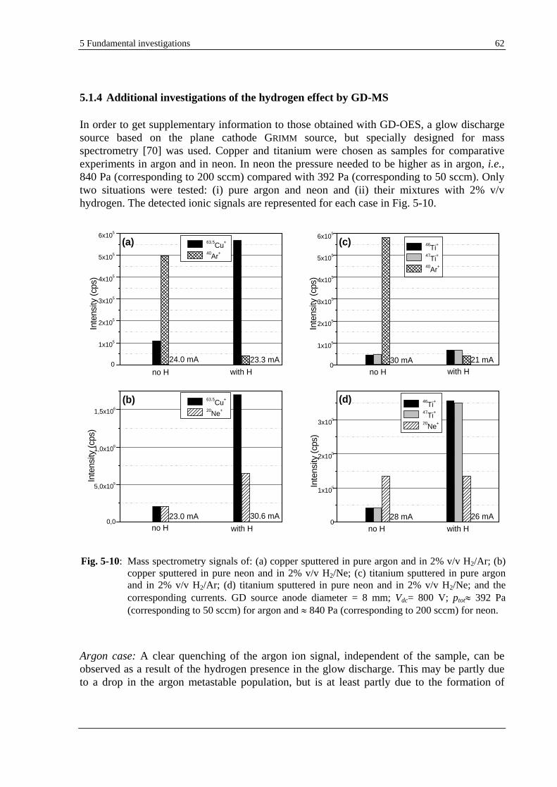
5 Fundamental investigations 62
5.1.4 Additional investigations of the hydrogen effect by GD-MS
In order to get supplementary information to those obtained with GD-OES, a glow discharge source based on the plane cathode GRIMM source, but specially designed for mass spectrometry [70] was used. Copper and titanium were chosen as samples for comparative experiments in argon and in neon. In neon the pressure needed to be higher as in argon, i.e., 840 Pa (corresponding to 200 sccm) compared with 392 Pa (corresponding to 50 sccm). Only two situations were tested: (i) pure argon and neon and (ii) their mixtures with 2% v/v hydrogen. The detected ionic signals are represented for each case in Fig. 5-10.
Argon case: A clear quenching of the argon ion signal, independent of the sample, can be observed as a result of the hydrogen presence in the glow discharge. This may be partly due to a drop in the argon metastable population, but is at least partly due to the formation of
Fig. 5-10: Mass spectrometry signals of: (a) copper sputtered in pure argon and in 2% v/v H2/Ar; (b) copper sputtered in pure neon and in 2% v/v H2/Ne; (c) titanium sputtered in pure argon and in 2% v/v H2/Ar; (d) titanium sputtered in pure neon and in 2% v/v H2/Ne; and thecorresponding currents. GD source anode diameter = 8 mm; Vdc= 800 V; ptot
392 Pa (corresponding to 50 sccm) for argon and 840 Pa (corresponding to 200 sccm) for neon.
0
1x10⁵
2x10⁵
3x10⁵
with H
with H
46Ti+
47Ti+
20Ne+
Inte
nsity
(cps
)
0
1x10⁵
2x10⁵
3x10⁵
4x10⁵
5x10⁵
6x10⁵
(d)
(c)
no H
no H
26 mA28 mA
21 mA30 mA
Inte
nsity
(cps
)
46Ti+
47Ti+
40Ar+
0,0
5,0x10⁵
1,0x10⁶
1,5x10⁶
(b)
63.5Cu+
20Ne+
Inte
nsity
(cps
)
0
1x10⁵
2x10⁵
3x10⁵
4x10⁵
5x10⁵
6x10⁵
(a)
with H
no H with H
no H
30.6 mA23.0 mA
23.3 mA24.0 mA
Inte
nsity
(cps
)
63.5Cu+
40Ar+
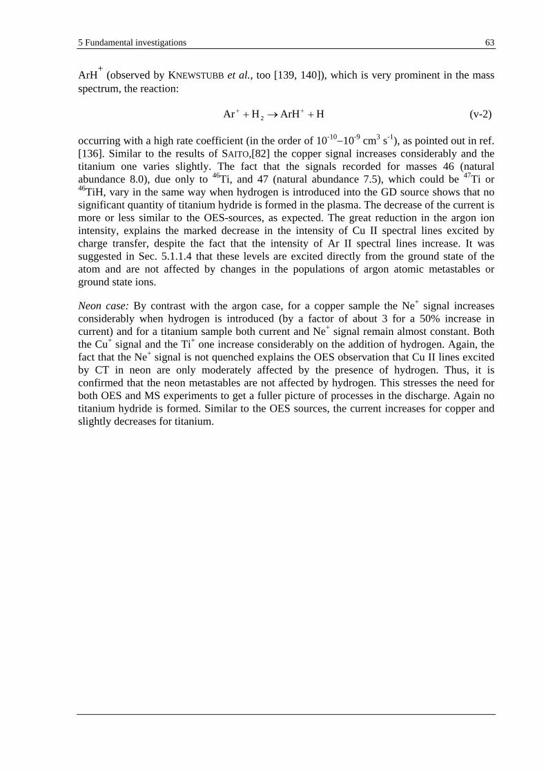
5 Fundamental investigations 63
ArH
+ (observed by KNEWSTUBB et al., too [139, 140]), which is very prominent in the mass
spectrum, the reaction:
H ArH H Ar 2
(v-2)
occurring with a high rate coefficient (in the order of 10-10 10-9 cm3 s-1), as pointed out in ref. [136]. Similar to the results of SAITO,[82] the copper signal increases considerably and the titanium one varies slightly. The fact that the signals recorded for masses 46 (natural abundance 8.0), due only to 46Ti, and 47 (natural abundance 7.5), which could be 47Ti or 46TiH, vary in the same way when hydrogen is introduced into the GD source shows that no significant quantity of titanium hydride is formed in the plasma. The decrease of the current is more or less similar to the OES-sources, as expected. The great reduction in the argon ion intensity, explains the marked decrease in the intensity of Cu II spectral lines excited by charge transfer, despite the fact that the intensity of Ar II spectral lines increase. It was suggested in Sec. 5.1.1.4 that these levels are excited directly from the ground state of the atom and are not affected by changes in the populations of argon atomic metastables or ground state ions.
Neon case: By contrast with the argon case, for a copper sample the Ne+ signal increases considerably when hydrogen is introduced (by a factor of about 3 for a 50% increase in current) and for a titanium sample both current and Ne+ signal remain almost constant. Both the Cu+ signal and the Ti+ one increase considerably on the addition of hydrogen. Again, the fact that the Ne+ signal is not quenched explains the OES observation that Cu II lines excited by CT in neon are only moderately affected by the presence of hydrogen. Thus, it is confirmed that the neon metastables are not affected by hydrogen. This stresses the need for both OES and MS experiments to get a fuller picture of processes in the discharge. Again no titanium hydride is formed. Similar to the OES sources, the current increases for copper and slightly decreases for titanium.
5 Fundamental investigations 64
5.1.5 Effect of hydrogen on line intensities of various analytes in common bulk materials (copper, low alloy steel, titanium, aluminium and silicon wafers)
A few years ago WÄNSTRAND and co-workers [141, 142] found by analysing of various carbides, nitrides and carbonitrides significant quantities of hydrogen coming from the deposition using hydrocarbon gases. Those measurements were carried out by A. BENGTSON
and are likely the very first results of quantified data of hydrogen by means of GD-OES. Just very recently a series of publications of various authors [4, 17, 18, 128, 143-145] shown that the presence of hydrogen in the GD plasma even in very small quantities (0.01% v/v) causes a considerable change in the intensities of most analytical lines and that changes can also be corrected for. However, due to the lack of reference materials containing hydrogen in certified quantities, (i) the corrections for the hydrogen effect on the other analytical lines, but (ii) especially the quantification of hydrogen itself cannot be considered as being in the final stage yet. Experimental data of changes occurred in the analyte intensities at the addition of small quantities of hydrogen are presented in the next subsections. Due to the large variations observed when hydrogen is present in the conventional carrier gas, i.e., argon, the same series of analytical lines were taken into account in a neon GD in hopes that the hydrogen effect takes place in a lower extent.
5.1.5.1 Effect of hydrogen on line intensities of various analytes when argon is the carrier gas
The intensity changes produced by the addition of hydrogen on various analytical emission lines - commonly used in the GD-OES routine analysis - are shown in Fig. 5-11. Maybe not so clearly to see in Fig. 5-11, but in further experiments in Sec. 5.1.7, one should state that the discharge current (as the dependent GD parameter) as well as the sputtering rate decrease significantly with the addition of small quantities of hydrogen. In view of the reduced current and sputtering rate (for more details see Sec. 5.1.7), lower intensities might be expected for lines of all elements apart from hydrogen. In general, the lines of most of the sputtered elements decrease, but at different rates. However, many Cu I lines increase in intensity when a massive copper sample is sputtered (Sec. 5.1.1.1).
The contrasting behaviour of the two Cu lines belonging to one and the same analyte caused by the presence of hydrogen (see Fig. 5-11a) confirms the same occurrence, however for the Cr I 305.4 and Cr I 425.4 nm lines found by BENGTSON and HÄNSTRÖM,[17] according to which individual excitation processes in the argon GD plasma are effected by hydrogen. The Ar I line 415.8 nm decreases as in Sec. 5.1.1.2 already shown (however over a larger range of hydrogen concentrations).
Looking at the Si I 288.1 nm line (Fig. 5-11e) it appears that this line is a special case, i.e., increase of the intensity of ~3 times at 0.1% hydrogen relative partial pressure. Therefore, an additional series of Si I lines was measured. Surprisingly, the intensities of all the strongest Si atomic emission lines behave very similar with that of the Si I 288.1 nm line. Possible explanations are given in Sec. 5.1.5.3.
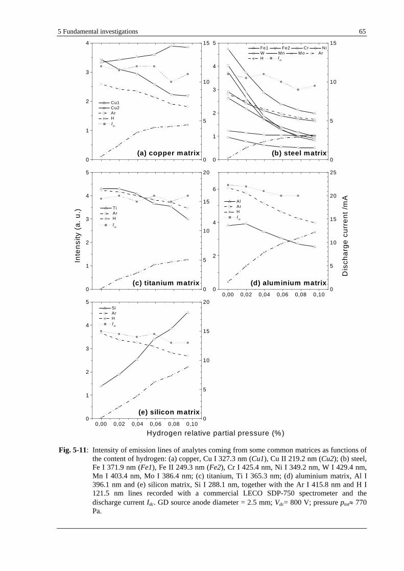
5 Fundamental investigations 65
Fig. 5-11: Intensity of emission lines of analytes coming from some common matrices as functions of the content of hydrogen: (a) copper, Cu I 327.3 nm (Cu1), Cu II 219.2 nm (Cu2); (b) steel, Fe I 371.9 nm (Fe1), Fe II 249.3 nm (Fe2), Cr I 425.4 nm, Ni I 349.2 nm, W I 429.4 nm, Mn I 403.4 nm, Mo I 386.4 nm; (c) titanium, Ti I 365.3 nm; (d) aluminium matrix, Al I 396.1 nm and (e) silicon matrix, Si I 288.1 nm, together with the Ar I 415.8 nm and H I 121.5 nm lines recorded with a commercial LECO SDP-750
spectrometer and the discharge current Idc. GD source anode diameter = 2.5 mm; Vdc= 800 V; pressure ptot
770 Pa.
0
1
2
3
4
(a) copper matrix
Cu1
Cu2
Ar
H
0
1
2
3
4
5
(b) steel matrix
Fe1
Fe2
Cr
Ni
W
Mn
Mo
Ar
H
0
1
2
3
4
5
Ti
Ar
H
(c) titanium matrix
Inte
nsi
ty (
a.
u.)
0,00 0,02 0,04 0,06 0,08 0,100
2
4
6
Al
Ar
H
(d) aluminium matrix
0,00 0,02 0,04 0,06 0,08 0,100
1
2
3
4
5
(e) silicon matrix
Hydrogen relative partial pressure (%)
Si
Ar
H
0
5
10
15
Idc
0
5
10
15
I
dc
0
5
10
15
20
Idc
0
5
10
15
20
25
Idc
Dis
cha
rge
curr
en
t /m
A
0
5
10
15
20
Idc
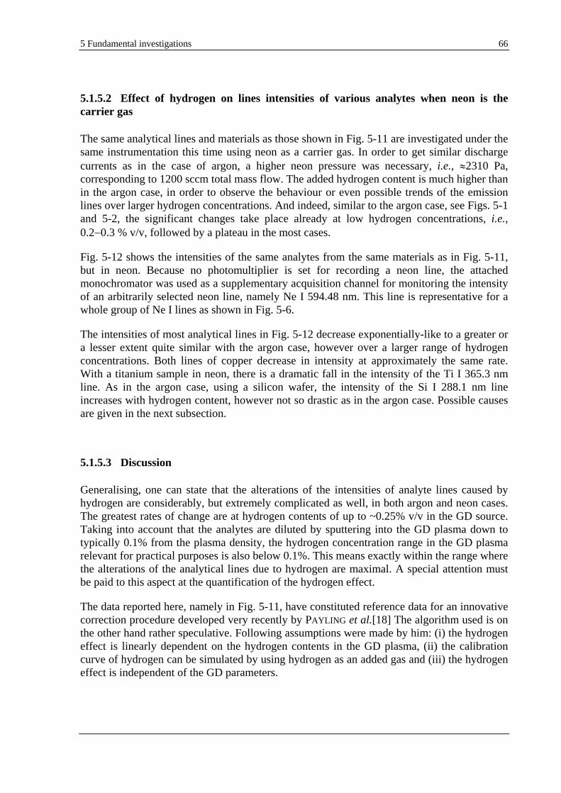
5 Fundamental investigations 66
5.1.5.2 Effect of hydrogen on lines intensities of various analytes when neon is the carrier gas
The same analytical lines and materials as those shown in Fig. 5-11 are investigated under the same instrumentation this time using neon as a carrier gas. In order to get similar discharge currents as in the case of argon, a higher neon pressure was necessary, i.e., 2310 Pa, corresponding to 1200 sccm total mass flow. The added hydrogen content is much higher than in the argon case, in order to observe the behaviour or even possible trends of the emission lines over larger hydrogen concentrations. And indeed, similar to the argon case, see Figs. 5-1 and 5-2, the significant changes take place already at low hydrogen concentrations, i.e., 0.2 0.3 % v/v, followed by a plateau in the most cases.
Fig. 5-12 shows the intensities of the same analytes from the same materials as in Fig. 5-11, but in neon. Because no photomultiplier is set for recording a neon line, the attached monochromator was used as a supplementary acquisition channel for monitoring the intensity of an arbitrarily selected neon line, namely Ne I 594.48 nm. This line is representative for a whole group of Ne I lines as shown in Fig. 5-6.
The intensities of most analytical lines in Fig. 5-12 decrease exponentially-like to a greater or a lesser extent quite similar with the argon case, however over a larger range of hydrogen concentrations. Both lines of copper decrease in intensity at approximately the same rate. With a titanium sample in neon, there is a dramatic fall in the intensity of the Ti I 365.3 nm line. As in the argon case, using a silicon wafer, the intensity of the Si I 288.1 nm line increases with hydrogen content, however not so drastic as in the argon case. Possible causes are given in the next subsection.
5.1.5.3 Discussion
Generalising, one can state that the alterations of the intensities of analyte lines caused by hydrogen are considerably, but extremely complicated as well, in both argon and neon cases. The greatest rates of change are at hydrogen contents of up to ~0.25% v/v in the GD source. Taking into account that the analytes are diluted by sputtering into the GD plasma down to typically 0.1% from the plasma density, the hydrogen concentration range in the GD plasma relevant for practical purposes is also below 0.1%. This means exactly within the range where the alterations of the analytical lines due to hydrogen are maximal. A special attention must be paid to this aspect at the quantification of the hydrogen effect.
The data reported here, namely in Fig. 5-11, have constituted reference data for an innovative correction procedure developed very recently by PAYLING et al.[18] The algorithm used is on the other hand rather speculative. Following assumptions were made by him: (i) the hydrogen effect is linearly dependent on the hydrogen contents in the GD plasma, (ii) the calibration curve of hydrogen can be simulated by using hydrogen as an added gas and (iii) the hydrogen effect is independent of the GD parameters.
5 Fundamental investigations 67
Fig. 5-12: Intensity of emission lines of analytes coming from some common matrices depending on the content of hydrogen: (a) copper, Cu I 327.3 nm (Cu1), Cu II 219.2 nm (Cu2); (b) steel, Fe I 371.9 nm (Fe1), Fe II 249.3 nm (Fe2), Cr I 425.4 nm, Ni I 349.2 nm, W I 429.4 nm, Mn I 403.4 nm, Mo I 386.4 nm; (c) titanium, Ti I 365.3 nm; (d) aluminium matrix, Al I 396.1 nm and (e) silicon matrix, Si I 288.1 nm, together with the Ne I 594.48 nm and H I 121.5 nm lines recorded with a commercial LECO SDP-750 spectrometer and the discharge current Idc. GD source anode diameter = 2.5 mm; Vdc= 1000 V; pressure ptot
2310 Pa.
0
1
2
3
4
5
(a) copper matrix
Cu1
Cu2
Ne
H
0
1
2
3
4
5
(b) steel matrix
Fe1
Fe2
Cr
Ni
W
Mn
Mo
Ne
H
0
1
2
3
4
5
6
Ti
Ne
H
(c) titanium matrix
Inte
nsi
ty (
a.
u.)
0,00 0,25 0,50 0,75 1,00 1,25 1,500
5
10
Al
Ne
H
(d) aluminium matrix
0,00 0,25 0,50 0,75 1,00 1,25 1,500
1
2
3
4
5
6
7
(e) silicon matrix
Hydrogen relative partial pressure (%)
Si
Ne
H
0
5
10
15
20
Idc
0
5
10
15
20
I
dc
0
5
10
15
20
Idc
0
10
20
30
Idc
Dis
cha
rge
curr
en
t /m
A
0
10
20
30
Idc
5 Fundamental investigations 68
If the first assumption could be accepted as being quite reasonable for practical purposes, the latter two ones are clarified just in the present work. Sec. 5.1.8 and 5.1.9 show that the latter two hypotheses are fortunately (!) true in a first approximation.
The general pattern of the hydrogen line(s) in dependence on the content is a considerable increase up to ~0.2% v/v hydrogen in the GD plasma, followed by a saturation or even slight decrease. As highlighted in Sec. 5.1.1.4, the results of WILKEN et al.,[32] who used powder pellets, can be also approximated in a linear calibration curve for hydrogen in the range below ~0.2% v/v hydrogen in the GD plasma. However, after a careful observation of the hydrogen line in Fig. 5-11, one can see that the dependence of its intensity on the hydrogen content is not linear, actually as in the results of WILKEN et al.,[32] too.
Nevertheless, PAYLING et al. [18] have liniarised the changes in the intensity of the analytical lines with the hydrogen content in the GD plasma (!), CHod, from Fig. 5-11. Hence, the emission yield, Ri, of an affected analytical line i includes the hydrogen effect in the following form:
HodHodi,i Ch 1 R , (v-3)
where hi,Hod is the slope of the dependencies from Fig. 5-11.
On the other hand, the changes in the intensities of analytical lines with the hydrogen signal (!), IH, can be monitored by each user at the analysis of samples containing hydrogen. In other words, one needs to monitor the hydrogen signal for at least one sample containing hydrogen. Again a linear dependence describes this time the hydrogen effect on an analytical line i with the measured hydrogen signal:
Hii Ih 1 R , (v-4)
where hi is the slope of the dependency. It remains only to re-scale the two dependencies:
HiHodHodi, Ih Ch , (v-5)
the scaling factor Hodi,i hh F
being enough to be determined only once, i.e., for an
analytical line.
Thus, by the PAYLING's concept it is possible to correct for the hydrogen effect on the analytical lines, using the dependencies from Fig. 5-11 and measuring only the hydrogen signal of the user itself. It is not necessary to know the amount of hydrogen in the samples used for calibration. The PAYLING's concept is already commercially available for the JOBIN-YVON machines.[146] On the other hand, the other two GD-OES spectrometer producers, LECO and SPECTRUMA, have also implemented a hydrogen correction based on a concept of BENGTSON.[147] Nevertheless, whereas the correction of the hydrogen effect on the analytical lines has been recording notably progresses, the quantification of hydrogen itself remains further a more problematic aspect. Efforts directed in the development of standards materials containing hydrogen of certified quantities are in progress.
Looking at the changes in the intensity of the analytical lines in both cases argon and neon, one can remark the huge increase of the Si I 288 nm line (excitation energy 5.08 eV) at the
5 Fundamental investigations 69
addition of hydrogen. Moreover, its behaviour is similar to silicon lines (in argon as well as in neon) with upper energies in the range 4.92 6.62 eV. Given the large energy range (1.7 eV), an energy selective excitation process can be excluded. This considerable increase of the intensity of the silicon lines is in conflict with the clear decrease of the sputtering rate and the discharge current in the presence of hydrogen (see Sec. 5.1.7). If the similarity in behaviour of the Si I lines to the hydrogen one in both argon and neon cases is taken into account, one can suggest that chemical processes having partners silicon and hydrogen can occur during sputtering or afterward in the GD plasma. Formation of new bindings such as silane could occur.[133, 148]
As expected from the explanations given in Sec. 5.1.2.2, the general pattern (of alteration) of the carrier gas line, Ar I 415.8 nm and Ne I 594.48 nm, respectively, when hydrogen is added to the GD, is almost independent of the matrix. Thus, the use of an argon line for the RF-GD-OES quantification [63, 64] of non-conductive samples which very often contain hydrogen must take care of the hydrogen effect (e.g., use of an Ar II line?).
From the practical analytical point of view, the increase of the intensity of some analytical lines and moreover linked to the decrease of the sputtering rate and discharge current, i.e., the increase of the emission yield, caused by the presence of small quantities of hydrogen in the GD plasma can be used to improve the sensitivity (emission yields) and even the detection limits of the corresponding analytes. Appropriate candidates for this might be for example: Si I 288.1 nm, Mg I 383.3 nm, Zn I 330.2 nm, Cu I 327.3 nm, etc. Chapter 6 presents some relevant examples of improving analytical performances by adding hydrogen to an argon GD.
It might be relevant to explain the use of the constant voltage/pressure mode in the measurements regarding the hydrogen affect presented till now. Firstly, it is much easier experimentally to control the hydrogen content in the GD plasma by gas mixing and so keeping the pressure and the voltage constant for various hydrogen concentrations than keeping the voltage and current constant and have defined hydrogen concentrations in the GD plasma. However, with corresponding effort various GD parameters and operating modes were tested, too. The results are presented in Sec. 5.1.9. Hence, the dependent GD-parameter, the discharge current, always decreases significantly already at hydrogen concentrations of ~0.1% v/v in argon for all the samples analysed. Section 5.1.7 will show that the use of neon as a carrier gas effects a much slighter decrease. If voltage and current are kept constant, then the pressure will vary by adding hydrogen. According to BENGTSON,[149] the changes in the pressure will not have a significant effect on the emission yields of the analytical lines. However, it will be shown in Sec. 5.1.9 that the changes in several analytical features caused by hydrogen are rather similar, independent of the GD parameters. Further extensive measurements are necessary.
On the other hand, the constant voltage/pressure mode is that working mode which is recommended for analysis of thin films. Trying to regulate the current by adjusting the pressure at the very beginning of a depth profile, where the GD source contamination is certainly present to a more or a lesser extent, will results in a faulty control of the GD-parameters.
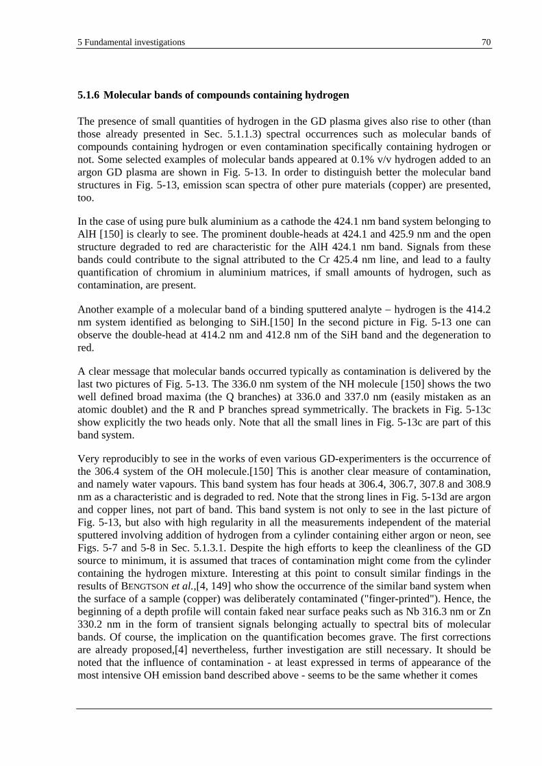
5 Fundamental investigations 70
5.1.6 Molecular bands of compounds containing hydrogen
The presence of small quantities of hydrogen in the GD plasma gives also rise to other (than those already presented in Sec. 5.1.1.3) spectral occurrences such as molecular bands of compounds containing hydrogen or even contamination specifically containing hydrogen or not. Some selected examples of molecular bands appeared at 0.1% v/v hydrogen added to an argon GD plasma are shown in Fig. 5-13. In order to distinguish better the molecular band structures in Fig. 5-13, emission scan spectra of other pure materials (copper) are presented, too.
In the case of using pure bulk aluminium as a cathode the 424.1 nm band system belonging to AlH [150] is clearly to see. The prominent double-heads at 424.1 and 425.9 nm and the open structure degraded to red are characteristic for the AlH 424.1 nm band. Signals from these bands could contribute to the signal attributed to the Cr 425.4 nm line, and lead to a faulty quantification of chromium in aluminium matrices, if small amounts of hydrogen, such as contamination, are present.
Another example of a molecular band of a binding sputtered analyte
hydrogen is the 414.2 nm system identified as belonging to SiH.[150] In the second picture in Fig. 5-13 one can observe the double-head at 414.2 nm and 412.8 nm of the SiH band and the degeneration to red.
A clear message that molecular bands occurred typically as contamination is delivered by the last two pictures of Fig. 5-13. The 336.0 nm system of the NH molecule [150] shows the two well defined broad maxima (the Q branches) at 336.0 and 337.0 nm (easily mistaken as an atomic doublet) and the R and P branches spread symmetrically. The brackets in Fig. 5-13c show explicitly the two heads only. Note that all the small lines in Fig. 5-13c are part of this band system.
Very reproducibly to see in the works of even various GD-experimenters is the occurrence of the 306.4 system of the OH molecule.[150] This is another clear measure of contamination, and namely water vapours. This band system has four heads at 306.4, 306.7, 307.8 and 308.9 nm as a characteristic and is degraded to red. Note that the strong lines in Fig. 5-13d are argon and copper lines, not part of band. This band system is not only to see in the last picture of Fig. 5-13, but also with high regularity in all the measurements independent of the material sputtered involving addition of hydrogen from a cylinder containing either argon or neon, see Figs. 5-7 and 5-8 in Sec. 5.1.3.1. Despite the high efforts to keep the cleanliness of the GD source to minimum, it is assumed that traces of contamination might come from the cylinder containing the hydrogen mixture. Interesting at this point to consult similar findings in the results of BENGTSON et al.,[4, 149] who show the occurrence of the similar band system when the surface of a sample (copper) was deliberately contaminated ("finger-printed"). Hence, the beginning of a depth profile will contain faked near surface peaks such as Nb 316.3 nm or Zn 330.2 nm in the form of transient signals belonging actually to spectral bits of molecular bands. Of course, the implication on the quantification becomes grave. The first corrections are already proposed,[4] nevertheless, further investigation are still necessary. It should be noted that the influence of contamination - at least expressed in terms of appearance of the most intensive OH emission band described above - seems to be the same whether it comes
5 Fundamental investigations 71
Fig. 5-13: Selected emission scan spectra recorded with a monochromator attached to a commercial LECO SDP-750 spectrometer showing some examples of molecular bands of hydrides (above) and contamination (below). For comparison spectra in pure argon and in 0.1% v/v hydrogen in argon are shown. GD source anode diameter = 2.5 mm; Vdc= 1000 V; pressure ptot 770 Pa.
410 411 412 413 414 4150
50
100
SiH
41
4.2
nm
Si, pure Ar
Si, 0.1% v/v H/Ar
Cu, pure Ar
Cu, 0.1% v/v H/Ar
Inte
nsi
ty (
a.
u.)
Wavelength /nm
423 424 425 426 427 428 429 4300
50
100
AlH
42
5.9
nm
AlH
42
4.1
nm
Al, pure Ar
Al, 0.1% v/v H/Ar
Cu, pure Ar
Cu, 0.1% v/v H/Ar
Inte
nsi
ty (
a.
u.)
330 331 332 333 334 335 336 337 338 339 340 341 342 3430
50
100
NH
33
7.0
nm
NH
33
6.0
nm
Cu, pure Ar
Cu, 0.1% v/v H/Ar
Inte
nsi
ty (
a.
u.)
305 310 315 3200
50
100
OH
30
6.4
nm
Cu, pure Ar
Cu, 0.1% v/v H/Ar
Inte
nsi
ty (
a.
u.)
Wavelength /nm
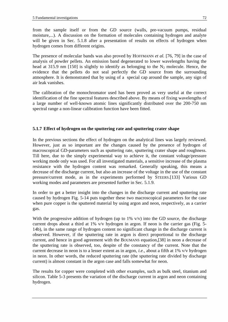
5 Fundamental investigations 72
from the sample itself or from the GD source (walls, pre-vacuum pumps, residual moisture,...). A discussion on the formation of molecules containing hydrogen and analyte will be given in Sec. 5.1.8 after a presentation of results on effects of hydrogen when hydrogen comes from different origins.
The presence of molecular bands was also proved by HOFFMANN et al. [76, 79] in the case of analysis of powder pellets. An emission band degenerated to lower wavelengths having the head at 315.9 nm [150] is slightly to identify as belonging to the N2 molecule. Hence, the evidence that the pellets do not seal perfectly the GD source from the surrounding atmosphere. It is demonstrated that by using of a special cap around the sample, any sign of air leak vanishes.
The calibration of the monochromator used has been proved as very useful at the correct identification of the fine spectral features described above. By means of fixing wavelengths of a large number of well-known atomic lines significantly distributed over the 200-750 nm spectral range a non-linear calibration function have been fitted.
5.1.7 Effect of hydrogen on the sputtering rate and sputtering crater shape
In the previous sections the effect of hydrogen on the analytical lines was largely reviewed. However, just as so important are the changes caused by the presence of hydrogen of macroscopical GD-parameters such as sputtering rate, sputtering crater shape and roughness. Till here, due to the simply experimental way to achieve it, the constant voltage/pressure working mode only was used. For all investigated materials, a sensitive increase of the plasma resistance with the hydrogen content was remarked. Generally speaking, this means a decrease of the discharge current, but also an increase of the voltage in the use of the constant pressure/current mode, as in the experiments performed by STEERS.[133] Various GD working modes and parameters are presented further in Sec. 5.1.9.
In order to get a better insight into the changes in the discharge current and sputtering rate caused by hydrogen Fig. 5-14 puts together these two macroscopical parameters for the case when pure copper is the sputtered material by using argon and neon, respectively, as a carrier gas.
With the progressive addition of hydrogen (up to 1% v/v) into the GD source, the discharge current drops about a third at 1% v/v hydrogen in argon. If neon is the carrier gas (Fig. 5-14b), in the same range of hydrogen content no significant change in the discharge current is observed. However, if the sputtering rate in argon is direct proportional to the discharge current, and hence in good agreement with the BOUMANS equation,[38] in neon a decrease of the sputtering rate is observed, too, despite of the constancy of the current. Note that the current decrease in neon is to a lesser extent as in argon, i.e., about a fifth at 1% v/v hydrogen in neon. In other words, the reduced sputtering rate (the sputtering rate divided by discharge current) is almost constant in the argon case and falls somewhat for neon.
The results for copper were completed with other examples, such as bulk steel, titanium and silicon. Table 5-3 presents the variation of the discharge current in argon and neon containing hydrogen.
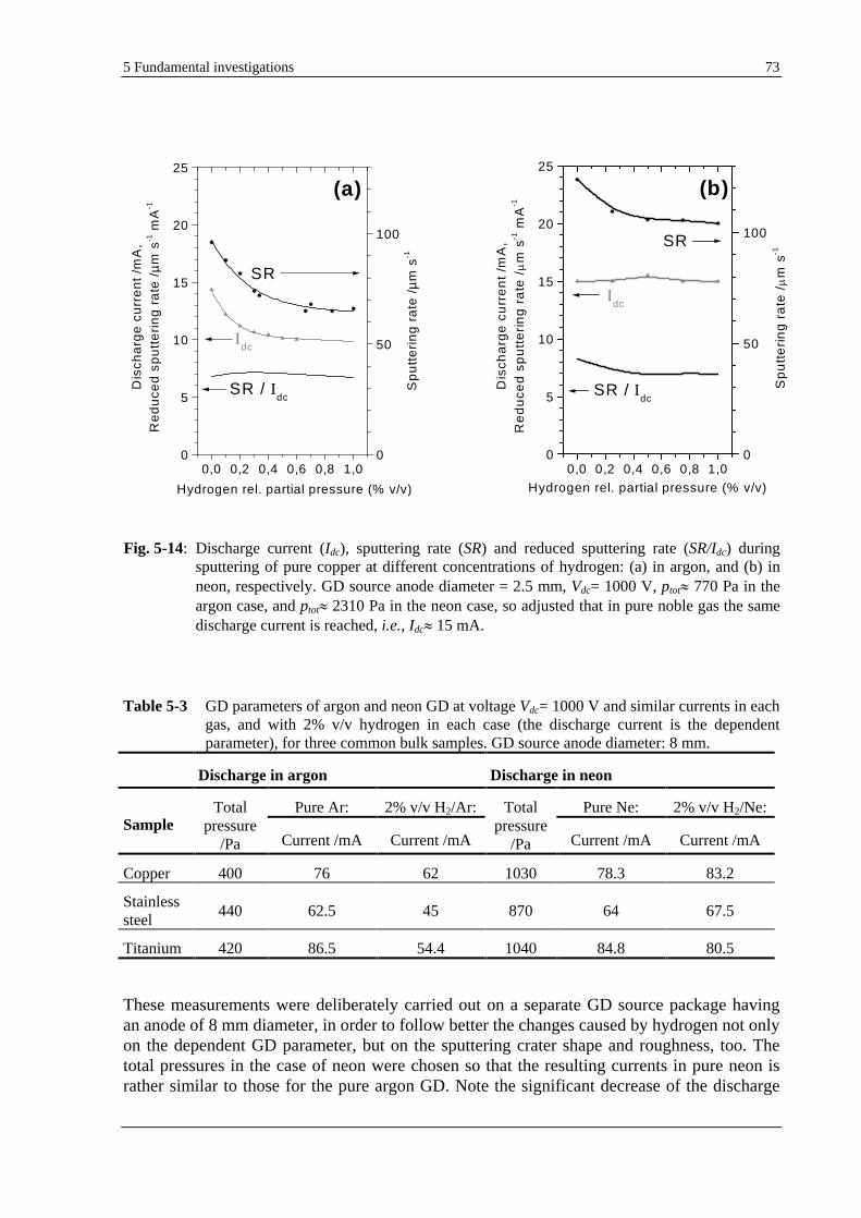
5 Fundamental investigations 73
Table 5-3 GD parameters of argon and neon GD at voltage Vdc= 1000 V and similar currents in each gas, and with 2% v/v hydrogen in each case (the discharge current is the dependent parameter), for three common bulk samples. GD source anode diameter: 8 mm.
Discharge in argon Discharge in neon
Pure Ar: 2% v/v H2/Ar: Pure Ne: 2% v/v H2/Ne:
Sample Total
pressure /Pa Current /mA Current /mA
Total pressure
/Pa Current /mA Current /mA
Copper 400 76 62 1030 78.3 83.2
Stainless steel
440 62.5 45 870 64 67.5
Titanium 420 86.5 54.4 1040 84.8 80.5
These measurements were deliberately carried out on a separate GD source package having an anode of 8 mm diameter, in order to follow better the changes caused by hydrogen not only on the dependent GD parameter, but on the sputtering crater shape and roughness, too. The total pressures in the case of neon were chosen so that the resulting currents in pure neon is rather similar to those for the pure argon GD. Note the significant decrease of the discharge
Fig. 5-14: Discharge current (Idc), sputtering rate (SR) and reduced sputtering rate (SR/Idc) during sputtering of pure copper
at different concentrations of hydrogen: (a) in argon, and (b) in neon, respectively. GD source anode diameter = 2.5 mm, Vdc= 1000 V, ptot
770 Pa in the argon case, and ptot
2310 Pa in the neon case, so adjusted that in pure noble gas the same discharge current is reached, i.e., Idc 15 mA.
0,0 0,2 0,4 0,6 0,8 1,00
5
10
15
20
25
D
isch
arg
e cu
rre
nt
/mA
,R
ed
uce
d sp
utt
eri
ng
rate
/µ
m s
-1 m
A-1
Hydrogen rel. partial pressure (% v/v)
0
50
100
(a)
SR / Idc
SR
Idc
Sp
utt
eri
ng
rate
/µ
m s
-1
0,0 0,2 0,4 0,6 0,8 1,00
5
10
15
20
25
SR / Idc
Idc
SR
Dis
cha
rge
curr
en
t /m
A,
Re
du
ced
spu
tte
rin
g ra
te /
m s
-1 m
A-1
Hydrogen rel. partial pressure (% v/v)
0
50
100
(b)
Sp
utt
eri
ng
rate
/m
s-1
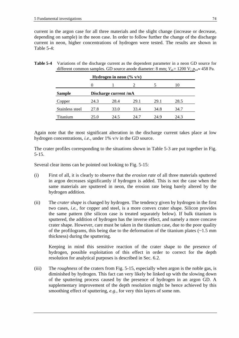
5 Fundamental investigations 74
current in the argon case for all three materials and the slight change (increase or decrease, depending on sample) in the neon case. In order to follow further the change of the discharge current in neon, higher concentrations of hydrogen were tested. The results are shown in Table 5-4:
Table 5-4 Variations of the discharge current as the dependent parameter in a neon GD source for different common samples. GD source anode diameter: 8 mm; Vdc= 1200 V; ptot 458 Pa.
Hydrogen in neon (% v/v)
0 1 2 5 10
Sample Discharge current /mA
Copper 24.3 28.4 29.1 29.1 28.5
Stainless steel 27.8 33.0 33.4 34.8 34.7
Titanium 25.0 24.5 24.7 24.9 24.3
Again note that the most significant alteration in the discharge current takes place at low hydrogen concentrations, i.e., under 1% v/v in the GD source.
The crater profiles corresponding to the situations shown in Table 5-3 are put together in Fig. 5-15.
Several clear items can be pointed out looking to Fig. 5-15:
(i) First of all, it is clearly to observe that the erosion rate of all three materials sputtered in argon decreases significantly if hydrogen is added. This is not the case when the same materials are sputtered in neon, the erosion rate being barely altered by the hydrogen addition.
(ii) The crater shape is changed by hydrogen. The tendency given by hydrogen in the first two cases, i.e., for copper and steel, is a more convex crater shape. Silicon provides the same pattern (the silicon case is treated separately below). If bulk titanium is sputtered, the addition of hydrogen has the inverse effect, and namely a more concave crater shape. However, care must be taken in the titanium case, due to the poor quality of the profilograms, this being due to the deformation of the titanium plates (~1.5 mm thickness) during the sputtering.
Keeping in mind this sensitive reaction of the crater shape to the presence of hydrogen, possible exploitation of this effect in order to correct for the depth resolution for analytical purposes is described in Sec. 6.2.
(iii) The roughness of the craters from Fig. 5-15, especially when argon is the noble gas, is diminished by hydrogen. This fact can very likely be linked up with the slowing down of the sputtering process caused by the presence of hydrogen in an argon GD. A supplementary improvement of the depth resolution might be hence achieved by this smoothing effect of sputtering, e.g., for very thin layers of some nm.
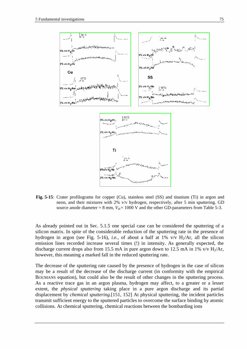
5 Fundamental investigations 75
As already pointed out in Sec. 5.1.5 one special case can be considered the sputtering of a silicon matrix. In spite of the considerable reduction of the sputtering rate in the presence of hydrogen in argon (see Fig. 5-16), i.e., of about a half at 1% v/v H2/Ar, all the silicon emission lines recorded increase several times (!) in intensity. As generally expected, the discharge current drops also from 15.5 mA in pure argon down to 12.5 mA in 1% v/v H2/Ar, however, this meaning a marked fall in the reduced sputtering rate.
The decrease of the sputtering rate caused by the presence of hydrogen in the case of silicon may be a result of the decrease of the discharge current (in conformity with the empirical BOUMANS equation), but could also be the result of other changes in the sputtering process. As a reactive trace gas in an argon plasma, hydrogen may affect, to a greater or a lesser extent, the physical sputtering taking place in a pure argon discharge and its partial displacement by chemical sputtering.[151, 152] At physical sputtering, the incident particles transmit sufficient energy to the sputtered particles to overcome the surface binding by atomic collisions. At chemical sputtering, chemical reactions between the bombarding ions
Fig. 5-15: Crater profilograms for copper (Cu), stainless steel (SS) and titanium (Ti) in argon and neon, and their mixtures with 2% v/v hydrogen, respectively, after 5 min sputtering. GD source anode diameter = 8 mm, Vdc= 1000 V and the other GD-parameters from Table 5-3.
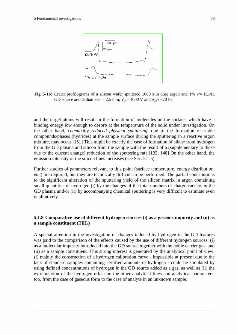
5 Fundamental investigations 76
and the target atoms will result in the formation of molecules on the surface, which have a binding energy low enough to desorb at the temperature of the solid under investigation. On the other hand, chemically reduced physical sputtering, due to the formation of stable compounds/phases (hydrides) at the sample surface during the sputtering in a reactive argon mixture, may occur.[151] This might be exactly the case of formation of silane from hydrogen from the GD plasma and silicon from the sample with the result of a (supplementary to those due to the current change) reduction of the sputtering rate.[133, 148] On the other hand, the emission intensity of the silicon lines increases (see Sec. 5.1.5).
Further studies of parameters relevant to this point (surface temperature, energy distribution, etc.) are required, but they are technically difficult to be performed. The partial contributions to the significant alteration of the sputtering yield of the silicon matrix in argon containing small quantities of hydrogen (i) by the changes of the total numbers of charge carriers in the GD plasma and/or (ii) by accompanying chemical sputtering is very difficult to estimate even qualitatively.
5.1.8 Comparative use of different hydrogen sources (i) as a gaseous impurity and (ii) as a sample constituent (TiH2)
A special attention in the investigation of changes induced by hydrogen in the GD features was paid to the comparison of the effects caused by the use of different hydrogen sources: (i) as a molecular impurity introduced into the GD source together with the noble carrier gas, and (ii) as a sample constituent. This strong interest is generated by the analytical point of view: (i) mainly the construction of a hydrogen calibration curve - impossible at present due to the lack of standard samples containing certified amounts of hydrogen - could be simulated by using defined concentrations of hydrogen in the GD source added as a gas, as well as (ii) the extrapolation of the hydrogen effect on the other analytical lines and analytical parameters, too, from the case of gaseous form to the case of analyte in an unknown sample.
Fig. 5-16: Crater profilograms of a silicon wafer sputtered 1000 s in pure argon and 1% v/v H2/Ar. GD source anode diameter = 2.5 mm, Vdc= 1000 V and ptot 670 Pa.
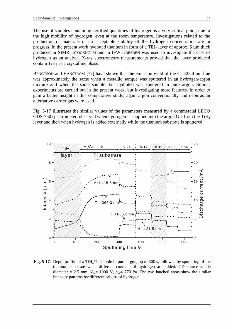
5 Fundamental investigations 77
The use of samples containing certified quantities of hydrogen is a very critical point, due to the high mobility of hydrogen, even at the room temperature. Investigations related to the production of materials of an acceptable stability of the hydrogen concentration are in progress. In the present work hydrated titanium in form of a TiH2 layer of approx. 5 µm thick produced in SIMR, STOCKHOLM and in IFW DRESDEN was used to investigate the case of hydrogen as an analyte. X-ray spectrometry measurements proved that the layer produced contain TiH2 as a crystalline phase.
BENGTSON and HÄNSTRÖM [17] have shown that the emission yield of the Cr 425.4 nm line was approximately the same when a metallic sample was sputtered in an hydrogen-argon mixture and when the same sample, but hydrated was sputtered in pure argon. Similar experiments are carried out in the present work, but investigating more features. In order to gain a better insight in this comparative study, again argon conventionally and neon as an alternative carrier gas were used.
Fig. 5-17 illustrates the similar values of the parameters measured by a commercial LECO GDS-750 spectrometer, observed when hydrogen is supplied into the argon GD from the TiH2
layer and then when hydrogen is added externally while the titanium substrate is sputtered.
Fig. 5-17: Depth profile of a TiH2/Ti sample in pure argon, up to 300 s, followed by sputtering of the titanium substrate when different contents of hydrogen are added. GD source anode diameter = 2.5 mm; Vdc= 1000 V, ptot
770 Pa. The two hatched areas show the similar intensity patterns for different origins of hydrogen.
0 100 200 300 400 500 6000
2
4
6
8
10H
2/Ar: 0 0.340.250.190.120.06
Ti substrateTiH
2
layer
H I 121.5 nm
H I 656.2 nm
Ti I 365.3 nm
Ar I 415.8 nm
Idc
Inte
nsi
ty (
a.
u.)
Sputtering time /s
0
5
10
15
20
25
Dis
cha
rge
curr
en
t /m
A
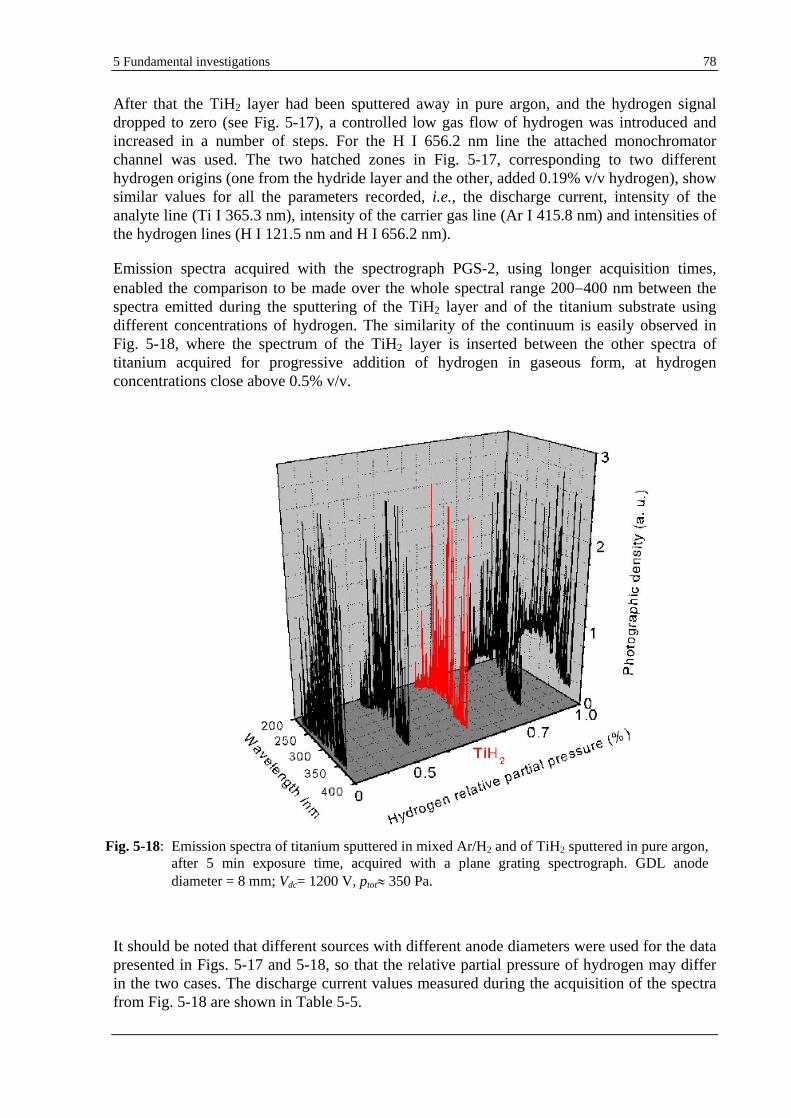
5 Fundamental investigations 78
After that the TiH2 layer had been sputtered away in pure argon, and the hydrogen signal dropped to zero (see Fig. 5-17), a controlled low gas flow of hydrogen was introduced and increased in a number of steps. For the H I 656.2 nm line the attached monochromator channel was used. The two hatched zones in Fig. 5-17, corresponding to two different hydrogen origins (one from the hydride layer and the other, added 0.19% v/v hydrogen), show similar values for all the parameters recorded, i.e., the discharge current, intensity of the analyte line (Ti I 365.3 nm), intensity of the carrier gas line (Ar I 415.8 nm) and intensities of the hydrogen lines (H I 121.5 nm and H I 656.2 nm).
Emission spectra acquired with the spectrograph PGS-2, using longer acquisition times, enabled the comparison to be made over the whole spectral range 200 400 nm between the spectra emitted during the sputtering of the TiH2 layer and of the titanium substrate using different concentrations of hydrogen. The similarity of the continuum is easily observed in Fig. 5-18, where the spectrum of the TiH2 layer is inserted between the other spectra of titanium acquired for progressive addition of hydrogen in gaseous form, at hydrogen concentrations close above 0.5% v/v.
It should be noted that different sources with different anode diameters were used for the data presented in Figs. 5-17 and 5-18, so that the relative partial pressure of hydrogen may differ in the two cases. The discharge current values measured during the acquisition of the spectra from Fig. 5-18 are shown in Table 5-5.
Fig. 5-18: Emission spectra of titanium sputtered in mixed Ar/H2 and of TiH2 sputtered in pure argon, after 5 min exposure time, acquired with a plane grating spectrograph. GDL anode diameter = 8 mm; Vdc= 1200 V, ptot 350 Pa.
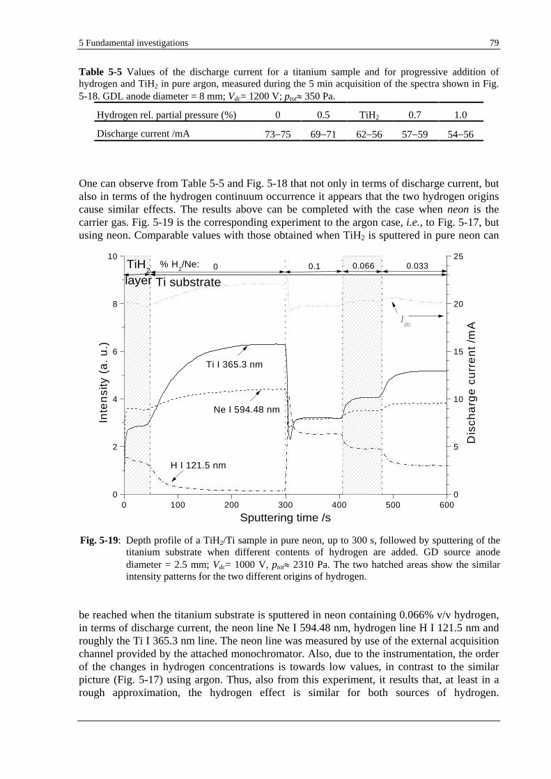
5 Fundamental investigations 79
Table 5-5 Values of the discharge current for a titanium sample and for progressive addition of hydrogen and TiH2 in pure argon, measured during the 5 min acquisition of the spectra shown in Fig. 5-18. GDL anode diameter = 8 mm; Vdc= 1200 V; ptot 350 Pa.
Hydrogen rel. partial pressure (%) 0 0.5 TiH2 0.7 1.0
Discharge current /mA 73 75 69 71 62 56 57 59 54 56
One can observe from Table 5-5 and Fig. 5-18 that not only in terms of discharge current, but also in terms of the hydrogen continuum occurrence it appears that the two hydrogen origins cause similar effects. The results above can be completed with the case when neon is the carrier gas. Fig. 5-19 is the corresponding experiment to the argon case, i.e., to Fig. 5-17, but using neon. Comparable values with those obtained when TiH2 is sputtered in pure neon can
be reached when the titanium substrate is sputtered in neon containing 0.066% v/v hydrogen, in terms of discharge current, the neon line Ne I 594.48 nm, hydrogen line H I 121.5 nm and roughly the Ti I 365.3 nm line. The neon line was measured by use of the external acquisition channel provided by the attached monochromator. Also, due to the instrumentation, the order of the changes in hydrogen concentrations is towards low values, in contrast to the similar picture (Fig. 5-17) using argon. Thus, also from this experiment, it results that, at least in a rough approximation, the hydrogen effect is similar for both sources of hydrogen.
Fig. 5-19: Depth profile of a TiH2/Ti sample in pure neon, up to 300 s, followed by sputtering of the titanium substrate when different contents of hydrogen are added. GD source anode diameter = 2.5 mm; Vdc= 1000 V, ptot
2310 Pa. The two hatched areas show the similar intensity patterns for the two different origins of hydrogen.
0 100 200 300 400 500 6000
2
4
6
8
10% H
2/Ne: 0 0.0330.0660.1
Ti substrate
TiH2
layer
H I 121.5 nm
Ti I 365.3 nm
Ne I 594.48 nm
Idc
Inte
nsi
ty (
a.
u.)
Sputtering time /s
0
5
10
15
20
25
Dis
cha
rge
curr
en
t /m
A
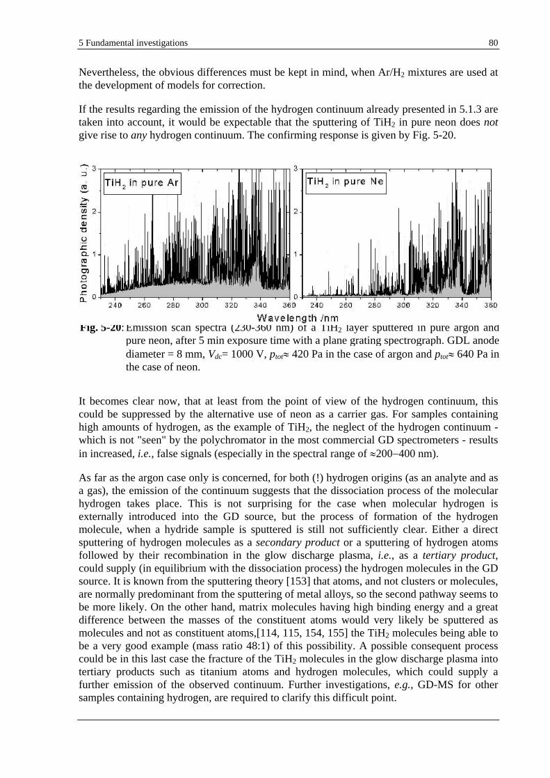
5 Fundamental investigations 80
Nevertheless, the obvious differences must be kept in mind, when Ar/H2 mixtures are used at the development of models for correction.
If the results regarding the emission of the hydrogen continuum already presented in 5.1.3 are taken into account, it would be expectable that the sputtering of TiH2 in pure neon does not give rise to any hydrogen continuum. The confirming response is given by Fig. 5-20.
It becomes clear now, that at least from the point of view of the hydrogen continuum, this could be suppressed by the alternative use of neon as a carrier gas. For samples containing high amounts of hydrogen, as the example of TiH2, the neglect of the hydrogen continuum - which is not "seen" by the polychromator in the most commercial GD spectrometers - results in increased, i.e., false signals (especially in the spectral range of 200 400 nm).
As far as the argon case only is concerned, for both (!) hydrogen origins (as an analyte and as a gas), the emission of the continuum suggests that the dissociation process of the molecular hydrogen takes place. This is not surprising for the case when molecular hydrogen is externally introduced into the GD source, but the process of formation of the hydrogen molecule, when a hydride sample is sputtered is still not sufficiently clear. Either a direct sputtering of hydrogen molecules as a secondary product or a sputtering of hydrogen atoms followed by their recombination in the glow discharge plasma, i.e., as a tertiary product, could supply (in equilibrium with the dissociation process) the hydrogen molecules in the GD source. It is known from the sputtering theory [153] that atoms, and not clusters or molecules, are normally predominant from the sputtering of metal alloys, so the second pathway seems to be more likely. On the other hand, matrix molecules having high binding energy and a great difference between the masses of the constituent atoms would very likely be sputtered as molecules and not as constituent atoms,[114, 115, 154, 155] the TiH2 molecules being able to be a very good example (mass ratio 48:1) of this possibility. A possible consequent process could be in this last case the fracture of the TiH2 molecules in the glow discharge plasma into tertiary products such as titanium atoms and hydrogen molecules, which could supply a further emission of the observed continuum. Further investigations, e.g., GD-MS for other samples containing hydrogen, are required to clarify this difficult point.
Fig. 5-20: Emission scan spectra (230-360 nm) of a TiH2
layer sputtered in pure argon and pure neon, after 5 min exposure time with a plane grating spectrograph. GDL anode diameter = 8 mm, Vdc= 1000 V, ptot 420 Pa in the case of argon and ptot 640 Pa in the case of neon.
5 Fundamental investigations 81
5.1.9 Influence of the GD parameters on the hydrogen effect
The conclusions on the hydrogen effect drawn till now are based on results obtained only at fixed GD working conditions, i.e., voltage and pressure were the GD parameters kept constant at rather arbitrary values. In other words, e.g., 1000 V and about 20 mA attained by regulating the pressure could be an extreme case of excitation for a GD source having an anode of only 2.5 mm diameter.[149] Therefore, in order to implement realistically empirical corrections for the effect of hydrogen on the other analytical lines the dependence of the effect on the GD parameters as well as on the working mode at all are necessary to be investigated. In the following two sections a few relevant analytical lines are selected as subject to thorough investigations.
5.1.9.1 Use of different operating modes
Zinc coated sheets are rather often analysed in the routine GD-OES. As will be shown later in chapter 6 the zinc coatings electrolytically plated contain considerable quantities of hydrogen. Moreover, the intensity of the 330.2 nm Zn line (as a conventional channel in many commercial GD-OES spectrometers) is enhanced in the presence of hydrogen. Therefore, the emission yield of this analytical line is evaluated at a complex variation of the GD parameters. Fig. 5-21 puts together the results obtained in two GD operating modes: (a) constant voltage/pressure and (b) constant voltage and current, at progressive addition of hydrogen to the argon GD plasma, both modes having as starting point the pure argon situation at Vdc= 700 V and Idc= 20 mA.
Firstly the already known operating mode constant voltage/pressure (Fig. 5-21a) is taken into account. As expected, the discharge current and the sputtering rate for zinc sputtered in argon at increasing hydrogen concentrations decrease in a manner similar to those of other materials presented in the previous sections. As the Zn 330.2 nm line intensity increases ~2 times at 1.2% v/v hydrogen, it follows that the emission yield (Y) - evaluated here as the measured intensity divided by the discharge current and sputtering rate - increases ~8 times at 1.2% v/v hydrogen. If one selects now the same voltage and currents as above, but in pure argon, the result is a decrease of the intensity (of course due to the decrease of the current) and overall a slight decrease of the emission yield (Y0). With other words, the emission yield of the Zn 330.2 nm line (Y0), rather unaffected by the change in the current, increases considerably (!) in the presence of hydrogen (at the same electrical GD parameters). A similar discrepancy is observed also between the sputtering crater forms in pure argon and in hydrogen/argon mixture, see Fig. 5-21a. The schematic crater profiles A, B and C show that hydrogen changes the profile o give a more convex crater; profiles A and D show the similar but smaller effect in pure argon caused by the same current change and the pressure change needed to reduce the current appropriately.
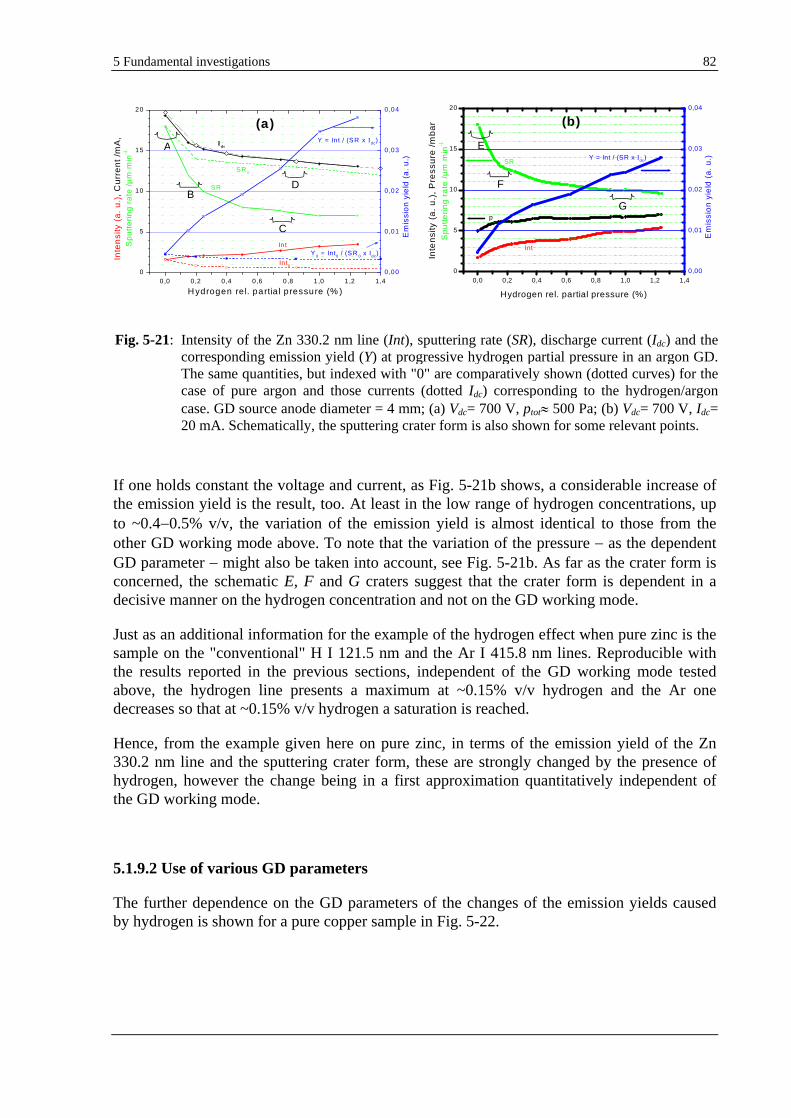
5 Fundamental investigations 82
If one holds constant the voltage and current, as Fig. 5-21b shows, a considerable increase of the emission yield is the result, too. At least in the low range of hydrogen concentrations, up to ~0.4 0.5% v/v, the variation of the emission yield is almost identical to those from the other GD working mode above. To note that the variation of the pressure
as the dependent GD parameter
might also be taken into account, see Fig. 5-21b. As far as the crater form is concerned, the schematic E, F and G craters suggest that the crater form is dependent in a decisive manner on the hydrogen concentration and not on the GD working mode.
Just as an additional information for the example of the hydrogen effect when pure zinc is the sample on the "conventional" H I 121.5 nm and the Ar I 415.8 nm lines. Reproducible with the results reported in the previous sections, independent of the GD working mode tested above, the hydrogen line presents a maximum at ~0.15% v/v hydrogen and the Ar one decreases so that at ~0.15% v/v hydrogen a saturation is reached.
Hence, from the example given here on pure zinc, in terms of the emission yield of the Zn 330.2 nm line and the sputtering crater form, these are strongly changed by the presence of hydrogen, however the change being in a first approximation quantitatively independent of the GD working mode.
5.1.9.2 Use of various GD parameters
The further dependence on the GD parameters of the changes of the emission yields caused by hydrogen is shown for a pure copper sample in Fig. 5-22.
Fig. 5-21: Intensity of the Zn 330.2 nm line (Int), sputtering rate (SR), discharge current (Idc) and the corresponding emission yield (Y) at progressive hydrogen partial pressure in an argon GD. The same quantities, but indexed with "0" are comparatively shown (dotted curves) for the case of pure argon and those currents (dotted Idc) corresponding to the hydrogen/argon case. GD source anode diameter = 4 mm; (a) Vdc= 700 V, ptot
500 Pa; (b) Vdc= 700 V, Idc= 20 mA. Schematically, the sputtering crater form is also shown for some relevant points.
0,0 0,2 0,4 0,6 0,8 1,0 1,2 1,40
5
10
15
20
Sp
utt
eri
ng
rate
/µ
m m
in-1
Y 0 = Int0 / (SR 0 x Idc)
In t0
SR 0
Idc
SR
Y = Int / (SR x Idc)
In t
Inte
nsi
ty (
a.
u.)
, C
urr
en
t /m
A,
H ydrogen re l. partia l pressure (% )
0,00
0,01
0,02
0,03
0,04
(a)
Em
issi
on
yie
ld (
a.
u.)
A
B
C
D
0,0 0,2 0,4 0,6 0,8 1,0 1,2 1,40
5
10
15
20
Sp
utt
eri
ng
rate
/µ
m m
in-1
(b)
Int
Inte
nsi
ty (
a.
u.)
, P
ress
ure
/m
ba
r
Hydrogen rel. partial pressure (%)
0,00
0,01
0,02
0,03
0,04
p
Y = Int / (SR x Idc)SR
Em
issi
on
yie
ld (
a.
u.)
E
F
G
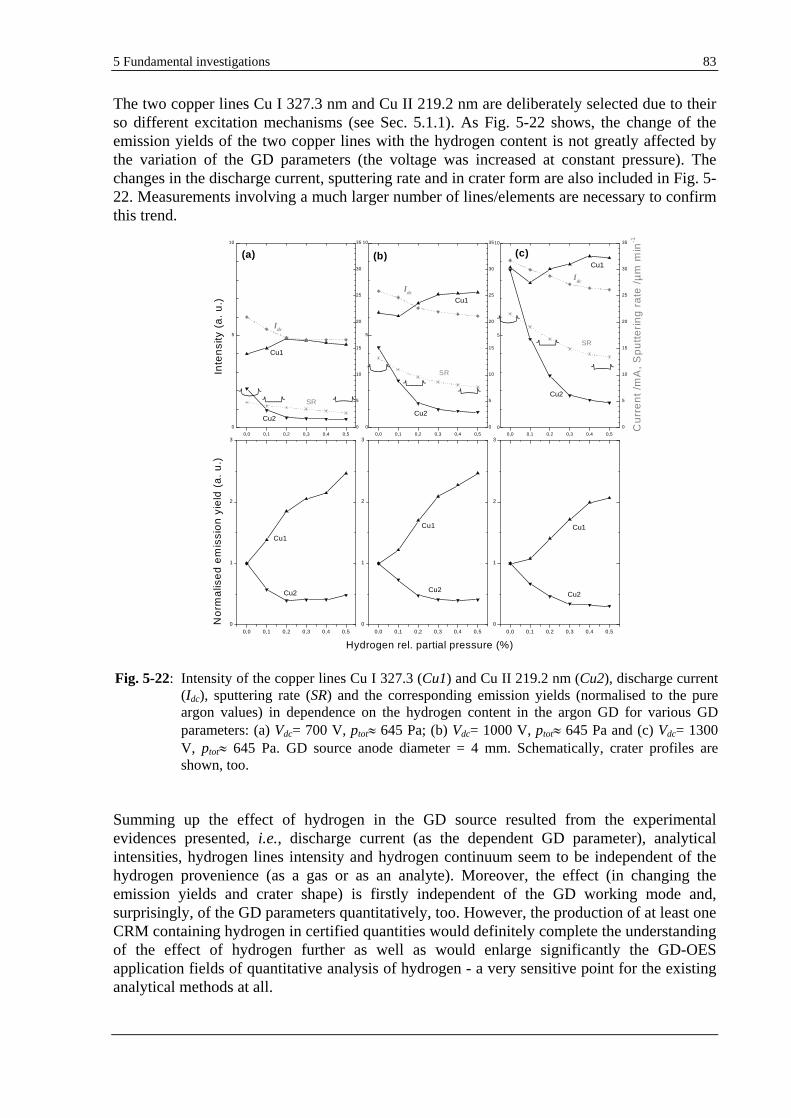
5 Fundamental investigations 83
The two copper lines Cu I 327.3 nm and Cu II 219.2 nm are deliberately selected due to their so different excitation mechanisms (see Sec. 5.1.1). As Fig. 5-22 shows, the change of the emission yields of the two copper lines with the hydrogen content is not greatly affected by the variation of the GD parameters (the voltage was increased at constant pressure). The changes in the discharge current, sputtering rate and in crater form are also included in Fig. 5-22. Measurements involving a much larger number of lines/elements are necessary to confirm this trend.
Summing up the effect of hydrogen in the GD source resulted from the experimental evidences presented, i.e., discharge current (as the dependent GD parameter), analytical intensities, hydrogen lines intensity and hydrogen continuum seem to be independent of the hydrogen provenience (as a gas or as an analyte). Moreover, the effect (in changing the emission yields and crater shape) is firstly independent of the GD working mode and, surprisingly, of the GD parameters quantitatively, too. However, the production of at least one CRM containing hydrogen in certified quantities would definitely complete the understanding of the effect of hydrogen further as well as would enlarge significantly the GD-OES application fields of quantitative analysis of hydrogen - a very sensitive point for the existing analytical methods at all.
Fig. 5-22: Intensity of the copper lines Cu I 327.3 (Cu1) and Cu II 219.2 nm (Cu2), discharge current (Idc), sputtering rate (SR) and the corresponding emission yields
(normalised to the pure argon values) in dependence on the hydrogen content in the argon GD for various GD parameters: (a) Vdc= 700 V, ptot
645 Pa; (b) Vdc= 1000 V, ptot
645 Pa and (c) Vdc= 1300 V, ptot
645 Pa. GD source anode diameter = 4 mm. Schematically, crater profiles are shown, too.
0,0 0,1 0,2 0,3 0,4 0,5
0
5
10
Cu2
Cu2
Cu1
Cu1
Idc
Idc
(b)(a)
Idc
Cu2
Cu1
(c)
Inte
nsi
ty (
a.
u.)
0,0 0,1 0,2 0,3 0,4 0,5
0
5
10
0,0 0,1 0,2 0,3 0,4 0,5
0
5
10
0
5
10
15
20
25
30
35
SR
SR
SR
0
5
10
15
20
25
30
35
0
5
10
15
20
25
30
35
Cu
rre
nt
/mA
, S
pu
tte
rin
g ra
te /
µm
min
-10,0 0,1 0,2 0,3 0,4 0,5
0
1
2
3
Cu2
Cu1
No
rma
lise
d e
mis
sio
n yi
eld
(a
. u
.)
0,0 0,1 0,2 0,3 0,4 0,5
0
1
2
3
Cu2
Cu1
Hydrogen rel. partial pressure (%)
0,0 0,1 0,2 0,3 0,4 0,5
0
1
2
3
Cu2
Cu1
5 Fundamental investigations 84
5.2 Depth profiling of thin multilayer coatings. Optimisation of the depth resolution
GD-OES was initially developed for the elemental analysis of bulk materials. However, as described in PRE-CONSIDERATIONS the main field of applications is nowadays the analysis of coatings. As a prerequisite for this kind of depth profiling technique, where the bombarding argon ions provide both the material sputtering and its subsequent excitation in the GD plasma, the optimisation of the GD plasma parameters with respect to the sputtering crater shape is necessary. The attaining of a flat sputtering crater, which guarantees the optimal depth resolution, may become time consuming when the investigated coatings are non-conductive or if they are thin layers. In many cases the attaining of a depth profile of multilayer stacks is even not possible at all. For example glass substrates of more than ~3 mm thickness are one of the biggest problems for the rf-generators commercially available. One very suggestive result is a inter-laboratory comparison launched by BAM on the "Evaluation of multilayer reference coatings for quantitative GD-OES depth profiling";[156] from 60 prospects interested in the analysis of a 5x(100 nm SiO2 / 100 nm TiO2) / BK7 glass (1 mm thick) sample only three (!) have been able to obtain reliable results.
In the next two sections are presented optimisation procedures for multilayer stacks of thin layers for GD-OES, and also for a competitive depth profiling technique, namely plasma SNMS. The process itself of deposition of the multilayer stacks can be on one hand controlled by GD-OES depth profiling, but on the other hand, such coatings can be used as reference coatings for GD-OES.
Thin layers such as Ti and Al were selected as conductive multilayer stacks, due to the very large application fields of Ti and Al and their compounds (TiN, TiC, AlN, Al2O3,...), e.g., adhesion, tribology, decorative coatings, high temperature and electronic applications, etc. Multilayer stacks of SiO2, TiO2, Si3N4 thin layers were selected as non-conductive materials for their dielectric, electronic, high temperature or wave guiding applications.
5.2.1 GD-OES procedure for the optimisation of the depth resolution
Especially in the rf-powering mode the optimisation procedure for depth profiling of multilayer coatings with respect to the depth resolution is laborious. An example of attaining the optimal depth resolution is selected for a 5x (250 nm Al / 50 nm Ti) / 100Cr6 steel sample, where a constant peak-to-peak voltage was applied and the argon pressure was varied as presented in Fig. 5-23. The same layer stack is resolved and quantified without considerable effort in the dc-mode.[157]
It should be noted that this driving mode (constant peak-to-peak voltage and pressure) of the GD plasma proved to be the most valuable for the free-running rf-generators. The rf measurement technique available does not allow a reliable control of the GD electrical parameters at the surface of the sputtered sample; therefore, the peak-to-peak voltage measured at the output rf-generator was selected as the steering rf-parameter.
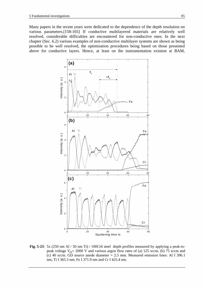
5 Fundamental investigations 85
Many papers in the recent years were dedicated to the dependence of the depth resolution on various parameters.[158-165] If conductive multilayered materials are relatively well resolved, considerable difficulties are encountered for non-conductive ones. In the next chapter (Sec. 6.2) various examples of non-conductive multilayer systems are shown as being possible to be well resolved, the optimisation procedures being based on those presented above for conductive layers. Hence, at least on the instrumentation existent at BAM,
Fig. 5-23: 5x (250 nm Al / 50 nm Ti) / 100Cr6 steel depth profiles measured by applying a peak-to-peak voltage Vpp= 2000 V and various argon flow rates of (a) 125 sccm, (b) 75 sccm and (c) 40 sccm. GD source anode diameter = 2.5 mm. Measured emission lines: Al I 396.1 nm; Ti I 365.3 nm; Fe I 371.9 nm and Cr I 425.4 nm.
0 20 40 60 800
2
4
6
(a)
Fe
TiAlt
c
ts
Inte
nsi
ty (
a.
u.)
0 20 40 60 800
2
4
6
(b)
Cr
FeAl Ti
Inte
nsi
ty (
a.
u.)
0 20 40 60 800
2
4
6
(c)
Cr
FeTiAl
Inte
nsi
ty (
a.
u.)
Sputtering time /s
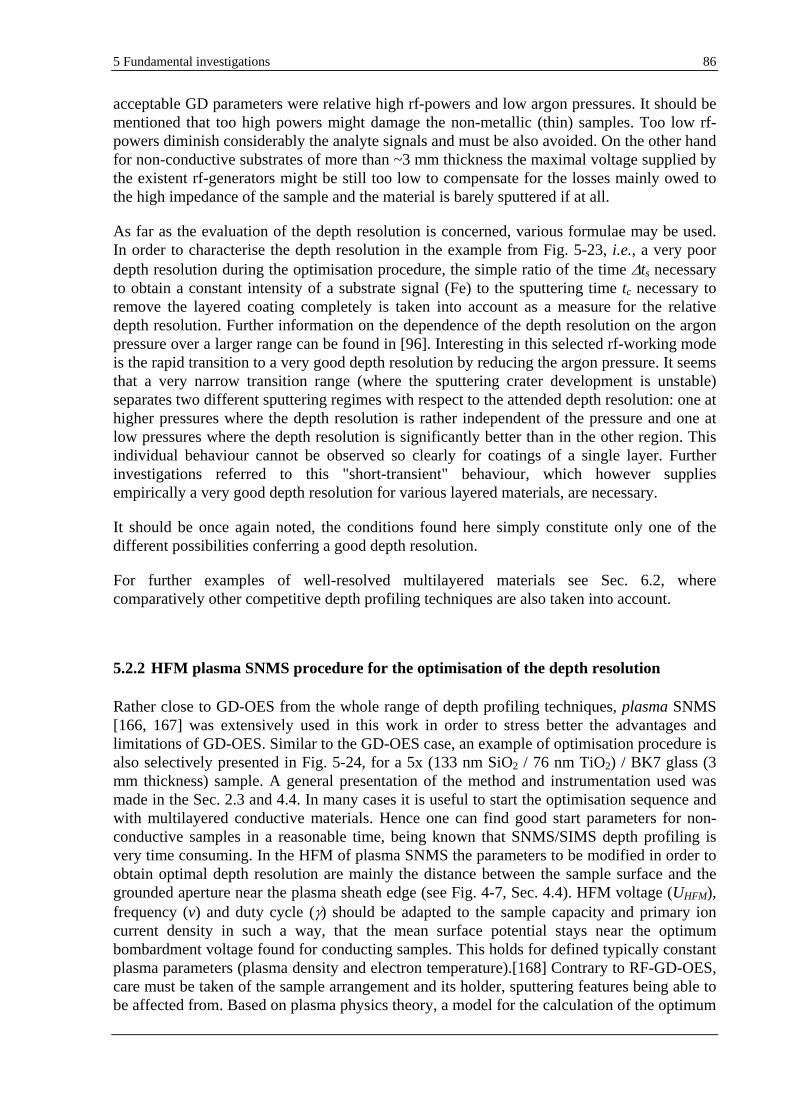
5 Fundamental investigations 86
acceptable GD parameters were relative high rf-powers and low argon pressures. It should be mentioned that too high powers might damage the non-metallic (thin) samples. Too low rf-powers diminish considerably the analyte signals and must be also avoided. On the other hand for non-conductive substrates of more than ~3 mm thickness the maximal voltage supplied by the existent rf-generators might be still too low to compensate for the losses mainly owed to the high impedance of the sample and the material is barely sputtered if at all.
As far as the evaluation of the depth resolution is concerned, various formulae may be used. In order to characterise the depth resolution in the example from Fig. 5-23, i.e., a very poor depth resolution during the optimisation procedure, the simple ratio of the time ts necessary to obtain a constant intensity of a substrate signal (Fe) to the sputtering time tc necessary to remove the layered coating completely is taken into account as a measure for the relative depth resolution. Further information on the dependence of the depth resolution on the argon pressure over a larger range can be found in [96]. Interesting in this selected rf-working mode is the rapid transition to a very good depth resolution by reducing the argon pressure. It seems that a very narrow transition range (where the sputtering crater development is unstable) separates two different sputtering regimes with respect to the attended depth resolution: one at higher pressures where the depth resolution is rather independent of the pressure and one at low pressures where the depth resolution is significantly better than in the other region. This individual behaviour cannot be observed so clearly for coatings of a single layer. Further investigations referred to this "short-transient" behaviour, which however supplies empirically a very good depth resolution for various layered materials, are necessary.
It should be once again noted, the conditions found here simply constitute only one of the different possibilities conferring a good depth resolution.
For further examples of well-resolved multilayered materials see Sec. 6.2, where comparatively other competitive depth profiling techniques are also taken into account.
5.2.2 HFM plasma SNMS procedure for the optimisation of the depth resolution
Rather close to GD-OES from the whole range of depth profiling techniques, plasma SNMS [166, 167] was extensively used in this work in order to stress better the advantages and limitations of GD-OES. Similar to the GD-OES case, an example of optimisation procedure is also selectively presented in Fig. 5-24, for a 5x (133 nm SiO2 / 76 nm TiO2) / BK7 glass (3 mm thickness) sample. A general presentation of the method and instrumentation used was made in the Sec. 2.3 and 4.4. In many cases it is useful to start the optimisation sequence and with multilayered conductive materials. Hence one can find good start parameters for non- conductive samples in a reasonable time, being known that SNMS/SIMS depth profiling is very time consuming. In the HFM of plasma SNMS the parameters to be modified in order to obtain optimal depth resolution are mainly the distance between the sample surface and the grounded aperture near the plasma sheath edge (see Fig. 4-7, Sec. 4.4). HFM voltage (UHFM), frequency (v) and duty cycle ( ) should be adapted to the sample capacity and primary ion current density in such a way, that the mean surface potential stays near the optimum bombardment voltage found for conducting samples. This holds for defined typically constant plasma parameters (plasma density and electron temperature).[168] Contrary to RF-GD-OES, care must be taken of the sample arrangement and its holder, sputtering features being able to be affected from. Based on plasma physics theory, a model for the calculation of the optimum
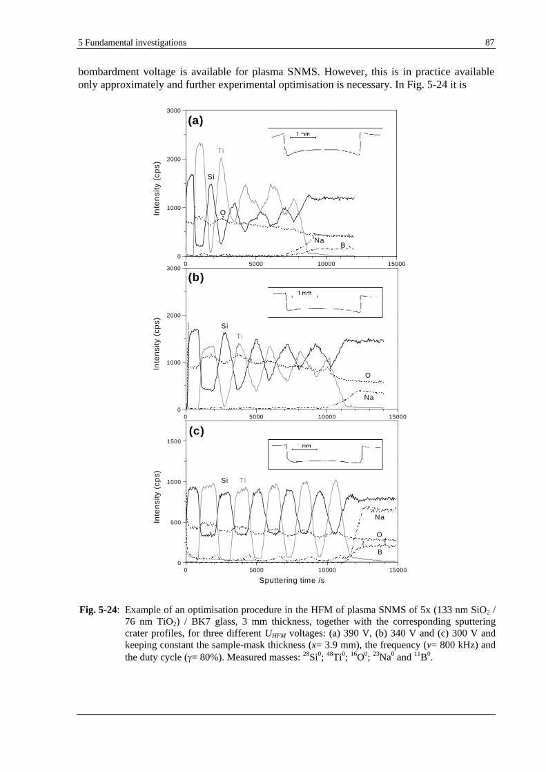
5 Fundamental investigations 87
bombardment voltage is available for plasma SNMS. However, this is in practice available only approximately and further experimental optimisation is necessary. In Fig. 5-24 it is
Fig. 5-24: Example of an optimisation procedure in the HFM of plasma SNMS of 5x (133 nm SiO2
/ 76 nm TiO2) / BK7 glass, 3 mm thickness, together with the corresponding sputtering crater profiles, for three different UHFM
voltages: (a) 390 V, (b) 340 V and (c) 300 V and keeping constant the sample-mask thickness (x= 3.9 mm), the frequency (v= 800 kHz) and the duty cycle ( = 80%). Measured masses: 28Si0; 48Ti0; 16O0; 23Na0 and 11B0.
0 5000 10000 150000
1000
2000
3000
BNa
O
Ti
Si
(a)
Inte
nsi
ty (
cps)
0 5000 10000 150000
1000
2000
3000
Na
O
Ti
Si
(b)
Inte
nsi
ty (
cps)
0 5000 10000 150000
500
1000
1500
B
Na
O
TiSi
(c)
Inte
nsi
ty (
cps)
Sputtering time /s
5 Fundamental investigations 88
presented an optimisation sequence carried out by changing the UHFM. The sample selected was 5x (133 nm SiO2 / 76 nm TiO2) / BK7 glass (3 mm thickness). Considering a rf-voltage as high as 390 V (see Fig. 5-24b), a convex sputtering crater is the result. Similar to the experience in GD-OES, a lower rf-voltage is needed. At UHFM= 340 V the depth resolution is improved and the convexity of the crater bottom is lowered. The optimum depth resolution was reached at UHFM= 300 V (see Fig. 5-24c). The flatness of the sputtering crater confirms this. A further decrease of the rf-voltage has significantly diminished the analytical intensities due to the very weak sputtering yields.
It should be noted that the Si signal detected in the case of plasma SNMS - by a quadrupole mass analyser - suffers from interference (contamination such as CO), the Si intensity being rather high in the TiO2 layers.
The variation of UHFM for a fixed distance between sample surface and grounded aperture described here for non-conductive materials is mainly the same as in the DBM (Direct Bombardment Mode) analysis of conductive samples.[169] However, an optimisation procedure for such thick non-conductive layers is nowhere detailed presented in the literature. Based on the procedure described above optimised depth profiles of other relevant layered non-conductive materials are presented in the next chapter (Sec. 6.2) by comparing competitive depth profiling techniques on some examples.
6 Applications in material science 89
6 Applications in material science
In the competition for the characterisation of thin films and coatings presenting combined interfaces between metals, semiconductors and insulators, GD-OES has established itself as a powerful analytical tool in determining the elemental composition and the layer thickness.[157, 159, 170, 171] The most important advantages of GD-OES against other depth profiling techniques such as SIMS, SNMS, AES, XPS, RBS, NRA are: low instrumentation and operational costs, high sample throughput (due to the high sputtering rate as well as no need of sample preparation), large range of analysed depth from several nm up to more than 100 µm, low detection limits in µg/g range or the possibility to acquire light elements such as H, C, N, O. However, taking into account the limitations of GD-OES, e.g., lateral resolution, chemical bonding information or depth resolution, GD-OES must be seen as an analytical technique which is complementary to the other ones and therefore essential in an analytical laboratory.
The next sections are intended to show the capabilities of GD-OES on some relevant examples. Three main directions are emphasised:
(i) The exploitation of the hydrogen effect on the intensity of those analytical lines whose emission yield is increased (see examples in Sec. 5.1) in order to improve analytical figures of merit such as sensitivity and detection limit (Sec. 6.1).
(ii) GD-OES depth profiling of multilayer systems of particular relevance, i.e., non-conductive thin layers and very thin layers (Sec. 6.2). The possibilities and limitations of the available GD-OES technique are discussed and compared selectively with other competitive analytical methods (Sec. 6.2.1). This time the hydrogen effect on the sputtering crater shape is exploited in order to improve the attained depth resolution (Sec. 6.2.2). It will be pointed out that especially very thin layers are able to be analysed by GD-OES, however under appropriate conditions. As Sec. 6.2.3 will show, the GD contamination (from the GD source itself, but also from the sample) consisting mainly of hydrogen, has to be brought under a critical level.
(iii) GD-OES depth profiling of thick coatings containing hydrogen (Sec. 6.3). Even if not quantitative, the GD-OES analysis of hydrogen in thick coatings, but at the coating/substrate interface and in the substrate as well proved to be very useful. Very often GD-OES is the single depth profiling technique able to be implemented at the analysis of such materials.
6.1 Improvement of sensitivity and detection limit in GD-OES by hydrogen addition
As emphasised largely for bulk materials in Sec. 5.1.5 and concretely exemplified on applications at the point (ii) in Sec. 6.2.2, there are emission lines, whose intensity is considerably enhanced by the hydrogen added to an argon GD. The following experiments try to demonstrate this quantitatively by using an appropriate set of CRMs. Fig. 6-1a shows in black a calibration curve of Mg contained as traces in a copper matrix. Two CRMs which do
6 Applications in material science 90
not contain Mg at all define the spectral background at 383.3 nm (the black dotted line at 0.29 a. u. in Fig. 6.1a). Adding deliberately 1.8% v/v hydrogen into the argon GD, so that beside the constant voltage the current remains the same, too, approximately 2.5 higher intensities of Mg I 383.3 nm are obtained.
As shown in Sec. 5.1.9, the sputtering rate, even at the same voltage and current, is reduced by hydrogen. Even though, taking into account that all the high purity copper CRMs used change the sputtering rate identically, not only higher signals, but also a slightly higher sensitivity are observed when hydrogen is added. The sensitivity is defined as the slope of the curves in Fig. 6-1. Hence, hydrogen increases slightly the sensitivity of the Mg I 383.3 nm line from 0.328 to 0.438 [(a. u.) / (µg g-1)]. Note that the arbitrary units on the ordinate in Fig. 6-1 are in fact Volt measured by the photomoltipliers of the LECO spectrometer. Actually, it was expected that the BAM-360 CRM having 4 µg/g Mg, which are not detected in pure argon (the black curve in Fig. 6-1a), might be separated from the background in the case of hydrogen addition (red curve in Fig. 6-1a). Unfortunately, this has not occurred, despite the improved sensitivity resulted and therefore, another example was taken into account.
Note that one could use the emission yield instead of sensitivity as defined above by its division to the sputtering rate. The emission yield is expected to increase more yet due to the reduced sputtering rate in the case of the addition of hydrogen.
A calibration curve for the Si I 288.1 nm line is plotted in Fig. 6-1b again for a set of pure copper CRMs. The background is defined this time by other two pure copper CRMs, which do not contain Si, i.e., the black dotted line at 0.039 a. u. in Fig. 6-1b. If one takes into account the IARM-78A sample, one can observe that the Si present as a trace is not differentiated from the background. However, if hydrogen is added to the argon GD, it is clearly observed that the IARM-78A fits excellently to the calibration curve (red curve in Fig. 6-1b). The intensity corresponding to 12 µg/g Si is in this case considerably above the background level. Thus, in Fig. 6-1b, the sensitivity of the Si I 288.1 nm line is drastically increased by hydrogen, approximately 8 times, from 0.09 to 0329 [(a. u.) / (µg g-1)]. Moreover, the detection limit of silicon is improved.
It makes sense to discuss the provenance of the enhanced background measured for both analytical lines in Figs. 6-1a and b, when hydrogen is added. As investigated extensively in Sec. 5.1.3, at hydrogen concentrations in argon plasma as high as 1.8% v/v, an intense hydrogen continuum is emitted over a large spectral range. Thus the measured line intensities at 383.3 nm and 288.1 nm, respectively, are superimposed by it. Nevertheless, this strong hydrogen continuum, being very stable in intensity, minimises the relative standard deviations of the measured line intensities corresponding to a very low range of analyte concentrations.
One could certainly go further with other examples of improved analytical figures of merit obtained by hydrogen addition. However these last two sections were intended to show only demonstratively that this is possible at all by a such unconventional, but efficient way.
6 Applications in material science 91
Fig. 6-1: Intensity of (a) Mg I 383.3 nm and (b) Si I 288.1 nm emission lines versus (a) Mg and (b) Si content, respectively, in CRMs of copper matrix in pure argon (black curves) and in hydrogen/argon mixture 1.8% v/v (red curves); dashed lines = level of the emission background; GD source anode diameter= 4 mm; Vdc= 700 V; Idc= 20 mA.
0 20 40 60 80 100 120 1400,0
0,1
0,2
0,3
0,4
0,5
0,6
H2/Ar
pure Ar
Si I 288.1 nm(b)
BAM-368
BAM-370
IARM-78ABAM-369
BAM-366
BAM-366
BAM-369
IARM-78ABAM-370
BAM-368
Inte
nsi
ty (
a.
u.)
Concentration /µg g-1
0 50 100 150 200 250 300 3500,0
0,5
1,0
1,5
pure Ar
H2/Ar
Mg I 383.3 nm(a)
BAM-367
BAM-367
BAM-368
BAM-369BAM-366
BAM-370
BAM-369
BAM-370BAM-366
BAM-368
Inte
nsi
ty (
a.
u.)
Concentration /µg g-1
6 Applications in material science 92
6.2 Exploitation of the hydrogen effect on GD-OES thin film analysis
The most thin layers used in industrial applications are electrically non-conductive. This makes necessary the use of the rf-excitation in order to be able to sputter the sample. On the other hand, the "start-up" contamination typically for GD-OES (at the beginning of a depth profile) worsens considerably the GD-OES analysis of thin and very thin layers. This section is dedicated to the study of the possibilities and limitations of the available GD-OES technique in thin film analysis. Comparative analytical methods are selectively used to inspect some relevant multilayer materials (Sec. 6.2.1). It will be shown (Sec. 6.2.2 and 6.2.3) that the attained depth resolution can be successfully improved in some cases and start-up phenomena reduced almost completely, if the effect of hydrogen is exploited and controlled, respectively. For conductive materials, where GD-OES quantified depth profiles are also shown (Sec. 6.2.3), the DC-GD-OES quantification was easily to perform.
6.2.1 Possibilities and limitations of GD-OES depth profiling of thin multilayer materials. Selective comparison with HFM plasma SNMS and ToF-SIMS
Sections 5.2.1 and 5.2.2 have already shown examples of optimisation sequences necessary to be performed when "difficult" materials such as very thin layers or especially thin non-conductive layers are GD-OES and SNMS, respectively, in-depth profiled. In this section other examples of already optimised depth profiles are also offered. The optimisation procedure is similar to those described in Sec. 5.2. However, each particular class of materials has its individual optimised conditions.
A 6 µm multilayer stack of 10, respectively 30 alternating CrAlN and CrN layers having individual thickness of 300 and 100 nm respectively were in depth profiled by RF-GD-OES. The sample were prepared by BAM VIII.2901. The optimised depth profiles are shown in Fig. 6-2a and b. Note that this type of ceramics is electrically conductive. Hence, the same GD parameters found to be optimal for the example shown in Sec. 5.2.1 for (Ti/Al)ML/steel were taken into account for the (CrAlN/CrN)ML/steel. The recorded sputtering crater profiles present a flat bottom corresponding to the attained depth resolution. Further details are described in [96, 170, 171]. Comparing the two Figs. 6-2a and b, it is easily to observe that the thinner layers (case b) are worse resolved, despite the same depth resolution. Note the poor sensitivity of the N signal.
It should also be noted that layer stacks of thickness in the µm range is well resolved by plasma SNMS, however, the time necessary to sputter the whole stack exceeding one normal working day. Hence, very thick coatings are not typical for plasma SNMS, the stability of the plasma becoming problematic over such long times of analysis.
6 Applications in material science 93
As described in Sec. 5.2, too, Si and Ti and their oxides and nitrides were selected for developing layered certified reference materials. Due to their manifold applications, the very stable oxides and nitrides are largely used in thin film technology. On the other hand, these systems were developed in BAM also in order to support step-by-step the GD-OES analysis of non-conductive layered materials. The difficulties encountered at the RF-GD-OES analysis of non-conductive layered systems can be overcome. For example, by using of these well-defined layered materials it is possible to check out the stability of the rf-generator.
The alternating thin layers SiO2 and TiO2 deposited on a BK7 glass by SCHOTT GLAS GMBH, Mainz, are maybe the most relevant example in the present investigation. The initial thickness of the glass substrate of 3 mm was adjusted down to 1 mm, a decisive aspect for the RF-GD-OES. The 3 mm glass substrate is barely sputtered at maximum applied rf-power with the instrumentation existent at BAM.
Optimised SNMS depth profiles obtained with both glass substrate thickness of 1 and 3 mm are comparatively presented in Fig. 6-3b and d. Note that under identical conditions of analysis, slight variations in sputtering time and depth resolution are found. However, due to the voltage fall on the sample, this dependence should be theoretically stronger. From these experiments it results that the Us voltage from Fig. 4-8, Sec. 4.4, which is in fact responsible for the sputtering of insulators, remains rather unchanged at different sample thickness ( Us= unchanged, too). A resistance parallel to the sample (possibly the plasma itself) seems to be the reason. Also the whole sample arrangement, especially in the case of non-conductive materials, is a critical point (see the experimental section, Sec. 4.4, Fig. 4-7). Considering the optimised RF-GD-OES profiles of the same samples shown in Fig. 6-3a and c, the substrate thickness was found this time to influence decisively the sputtering rate. The voltage loss influence across an insulator sample, being proportional to the thickness, effects lower sputtering rates for thicker samples. It takes approximately four times longer to profile in-
Fig. 6-2: Typical optimised RF-GD-OES qualitative depth profiles of the multilayers structures: (a) 10x (300 nm CrAlN / 300 nm CrN) / 100Cr6 steel and (b) 30x (100 nm CrAlN / 100 nm CrN) / 100Cr6 steel. Vpp= 2000 V and Ar flow rate = 40 sccm; GD source anode diameter = 2.5 mm. Measured emission lines: Cr I 425.4 nm; Al I 396.1 nm; N I 149.2 nm and Fe I 371.9 nm.
0 100 200 300 400 5000
2
4
6
8
10
(a)
N
Fe
CrAl
Inte
nsi
ty (
a.
u.)
Sputtering time /s
0 100 200 300 4000
2
4
6
8
10
(b)
N
FeAlCr
Inte
nsi
ty (
a.
u.)
Sputtering time /s
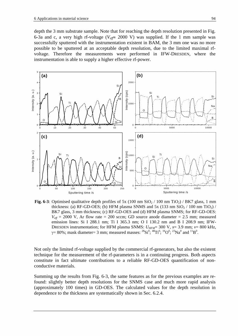
6 Applications in material science 94
depth the 3 mm substrate sample. Note that for reaching the depth resolution presented in Fig. 6-3a and c, a very high rf-voltage (Veff
2000 V) was supplied. If the 1 mm sample was
successfully sputtered with the instrumentation existent in BAM, the 3 mm one was no more possible to be sputtered at an acceptable depth resolution, due to the limited maximal rf-voltage. Therefore the measurements were performed in IFW-DRESDEN, where the instrumentation is able to supply a higher effective rf-power.
Not only the limited rf-voltage supplied by the commercial rf-generators, but also the existent technique for the measurement of the rf-parameters is in a continuing progress. Both aspects constitute in fact ultimate contributions to a reliable RF-GD-OES quantification of non-conductive materials.
Summing up the results from Fig. 6-3, the same features as for the previous examples are re-found: slightly better depth resolutions for the SNMS case and much more rapid analysis (approximately 100 times) in GD-OES. The calculated values for the depth resolution in dependence to the thickness are systematically shown in Sec. 6.2.4.
Fig. 6-3: Optimised qualitative depth profiles of 5x (100 nm SiO2 / 100 nm TiO2) / BK7 glass, 1 mm thickness: (a) RF-GD-OES; (b) HFM plasma SNMS and 5x (133 nm SiO2 / 100 nm TiO2) / BK7 glass, 3 mm thickness; (c) RF-GD-OES and (d) HFM plasma SNMS; for RF-GD-OES: Veff
= 2000 V, Ar flow rate = 200 sccm; GD source anode diameter = 2.5 mm; measured emission lines: Si I 288.1 nm; Ti I 365.3 nm; O I 130.2 nm and B I 208.9 nm; IFW-DRESDEN instrumentation; for HFM plasma SNMS: UHFM= 300 V, x= 3.9 mm; v=
800 kHz, = 80%; mask diameter= 3 mm; measured masses: 28Si0; 48Ti0; 16O0; 23Na0 and 11B0.
0 5000 100000
1000
2000
Na
B
O
SiTi
Si
(b)
Inte
nsi
ty (
cps)
0 10 20 30 40 500
1
2
3
4
5
Si
B
OO
Ti
Si
(a)
Inte
nsi
ty (
a.
u.)
0 50 100 150 200 2500
1
2
OO
B
Si
TiSi
(c)
Inte
nsi
ty (
a.
u.)
Sputtering time /s
0 5000 100000
500
1000
1500
Na
B
Si
O
TiSi
(d)
Inte
nsi
ty (
cps)
Sputtering time /s
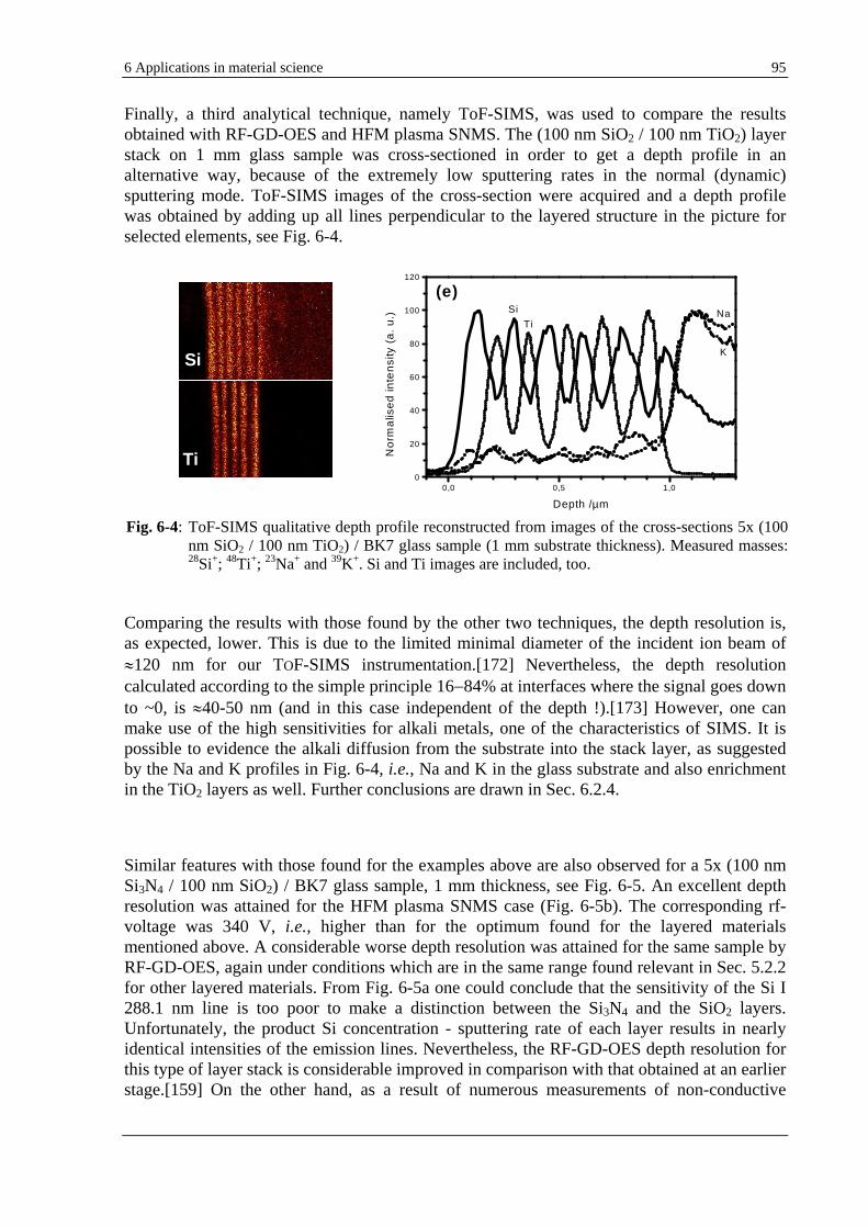
6 Applications in material science 95
Finally, a third analytical technique, namely ToF-SIMS, was used to compare the results obtained with RF-GD-OES and HFM plasma SNMS. The (100 nm SiO2 / 100 nm TiO2) layer stack on 1 mm glass sample was cross-sectioned in order to get a depth profile in an alternative way, because of the extremely low sputtering rates in the normal (dynamic) sputtering mode. ToF-SIMS images of the cross-section were acquired and a depth profile was obtained by adding up all lines perpendicular to the layered structure in the picture for selected elements, see Fig. 6-4.
Comparing the results with those found by the other two techniques, the depth resolution is, as expected, lower. This is due to the limited minimal diameter of the incident ion beam of
120 nm for our TOF-SIMS instrumentation.[172] Nevertheless, the depth resolution calculated according to the simple principle 16 84% at interfaces where the signal goes down to ~0, is 40-50 nm (and in this case independent of the depth !).[173] However, one can make use of the high sensitivities for alkali metals, one of the characteristics of SIMS. It is possible to evidence the alkali diffusion from the substrate into the stack layer, as suggested by the Na and K profiles in Fig. 6-4, i.e., Na and K in the glass substrate and also enrichment in the TiO2 layers as well. Further conclusions are drawn in Sec. 6.2.4.
Similar features with those found for the examples above are also observed for a 5x (100 nm Si3N4 / 100 nm SiO2) / BK7 glass sample, 1 mm thickness, see Fig. 6-5. An excellent depth resolution was attained for the HFM plasma SNMS case (Fig. 6-5b). The corresponding rf-voltage was 340 V, i.e., higher than for the optimum found for the layered materials mentioned above. A considerable worse depth resolution was attained for the same sample by RF-GD-OES, again under conditions which are in the same range found relevant in Sec. 5.2.2 for other layered materials. From Fig. 6-5a one could conclude that the sensitivity of the Si I 288.1 nm line is too poor to make a distinction between the Si3N4 and the SiO2 layers. Unfortunately, the product Si concentration - sputtering rate of each layer results in nearly identical intensities of the emission lines. Nevertheless, the RF-GD-OES depth resolution for this type of layer stack is considerable improved in comparison with that obtained at an earlier stage.[159] On the other hand, as a result of numerous measurements of non-conductive
Fig. 6-4: ToF-SIMS qualitative depth profile reconstructed from images of the cross-sections 5x (100 nm SiO2 / 100 nm TiO2) / BK7 glass sample (1 mm substrate thickness). Measured masses: 28Si+; 48Ti+; 23Na+ and 39K+. Si and Ti images are included, too.
0,0 0,5 1,00
20
40
60
80
100
120
(e)
K
NaTi
Si
No
rma
lise
d in
ten
sity
(a
. u
.)
Depth /µm
Si
Ti
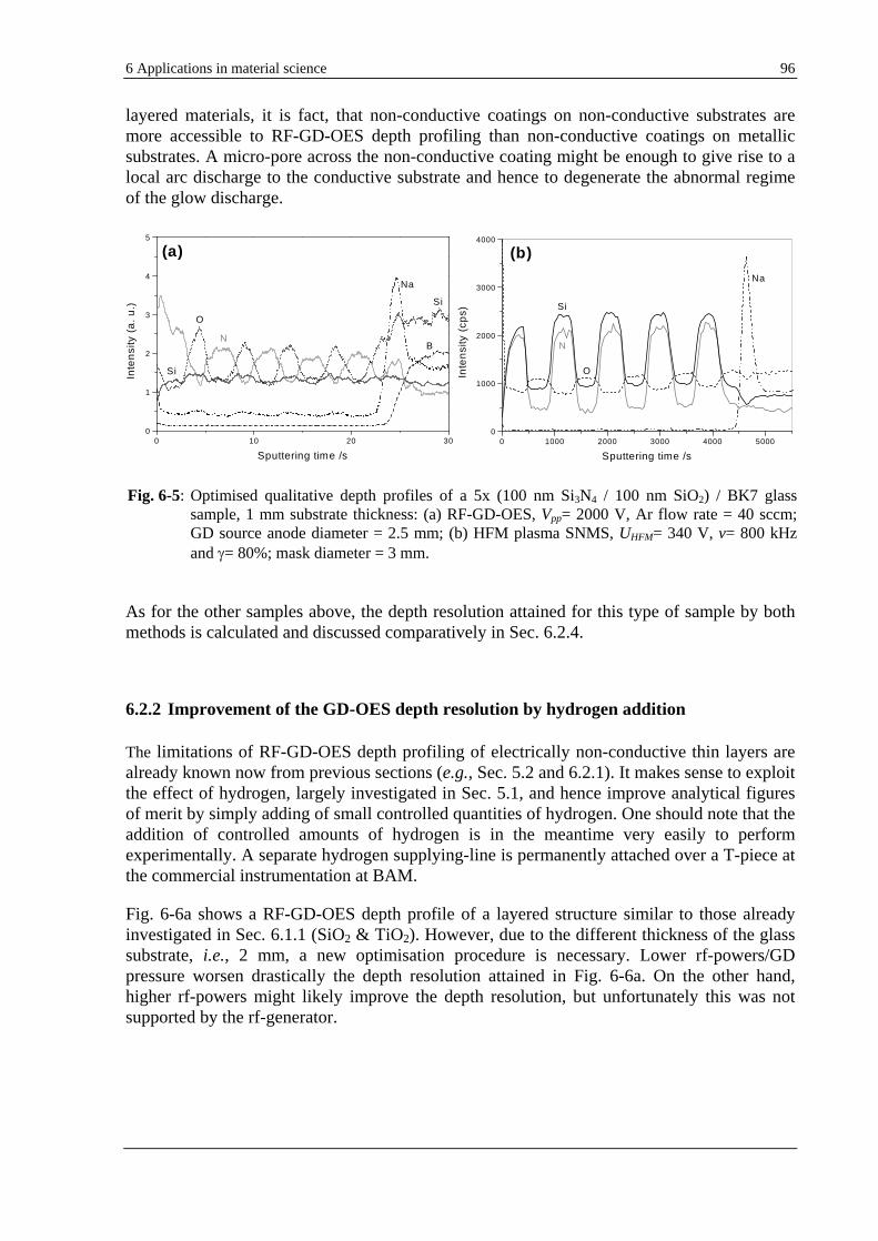
6 Applications in material science 96
layered materials, it is fact, that non-conductive coatings on non-conductive substrates are more accessible to RF-GD-OES depth profiling than non-conductive coatings on metallic substrates. A micro-pore across the non-conductive coating might be enough to give rise to a local arc discharge to the conductive substrate and hence to degenerate the abnormal regime of the glow discharge.
As for the other samples above, the depth resolution attained for this type of sample by both methods is calculated and discussed comparatively in Sec. 6.2.4.
6.2.2 Improvement of the GD-OES depth resolution by hydrogen addition
The limitations of RF-GD-OES depth profiling of electrically non-conductive thin layers are already known now from previous sections (e.g., Sec. 5.2 and 6.2.1). It makes sense to exploit the effect of hydrogen, largely investigated in Sec. 5.1, and hence improve analytical figures of merit by simply adding of small controlled quantities of hydrogen. One should note that the addition of controlled amounts of hydrogen is in the meantime very easily to perform experimentally. A separate hydrogen supplying-line is permanently attached over a T-piece at the commercial instrumentation at BAM.
Fig. 6-6a shows a RF-GD-OES depth profile of a layered structure similar to those already investigated in Sec. 6.1.1 (SiO2 & TiO2). However, due to the different thickness of the glass substrate, i.e., 2 mm, a new optimisation procedure is necessary. Lower rf-powers/GD pressure worsen drastically the depth resolution attained in Fig. 6-6a. On the other hand, higher rf-powers might likely improve the depth resolution, but unfortunately this was not supported by the rf-generator.
Fig. 6-5: Optimised qualitative depth profiles of a 5x (100 nm Si3N4 / 100 nm SiO2) / BK7 glass sample, 1 mm substrate thickness: (a) RF-GD-OES, Vpp= 2000 V, Ar flow rate = 40 sccm; GD source anode diameter = 2.5 mm; (b) HFM plasma SNMS, UHFM= 340 V, v= 800 kHz and = 80%; mask diameter = 3 mm.
0 1000 2000 3000 4000 50000
1000
2000
3000
4000
Na
O
Si
N
(b)
Inte
nsi
ty (
cps)
Sputtering time /s
0 10 20 300
1
2
3
4
5
Si
O
Na
B
Si
N
(a)
Inte
nsi
ty (
a.
u.)
Sputtering time /s
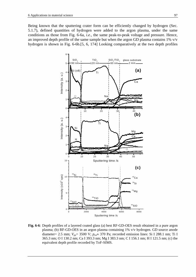
6 Applications in material science 97
Being known that the sputtering crater form can be efficiently changed by hydrogen (Sec. 5.1.7), defined quantities of hydrogen were added to the argon plasma, under the same conditions as those from Fig. 6-6a, i.e., the same peak-to-peak voltage and pressure. Hence, an improved depth profile of the same sample but when the argon GD plasma contains 1% v/v hydrogen is shown in Fig. 6-6b.[5, 6, 174] Looking comparatively at the two depth profiles
Fig. 6-6: Depth profiles of a layered coated glass (a) best RF-GD-OES result obtained in a pure argon plasma; (b) RF-GD-OES in an argon plasma containing 1% v/v hydrogen. GD source anode diameter= 2.5 mm; Vpp= 3500 V; ptot
370 Pa; recorded emission lines: Si I 288.1 nm; Ti I 365.3 nm; O I 130.2 nm; Ca I 393.3 nm; Mg I 383.3 nm; C I 156.1 nm; H I 121.5 nm; (c) the equivalent depth profile recorded by ToF-SIMS.
0 10 20 30 40 500
1
2
3
4
5
6
(b)
ONaC
Mg
HCa
Ti
Si
Inte
nsi
ty (
a.
u.)
Sputtering time /s
0 2000 4000 6000 80000
5
10
15
44SiO
28Si
(c)
44SiO
64TiO
16O x10
24Mg
40Ca
48Ti28Si
Inte
nsi
ty (
x10
3 cp
s)
Sputtering time /s
0 10 20 30 400
1
2
3
4
5
6
glass substrate2 mm
SiO2/TiO
2
60 nmTiO
2
120 nmSiO
2
90 nm
MgH
C
O Na
Ca
(a)Ti
Si (x8)
Inte
nsi
ty (
a.
u.)
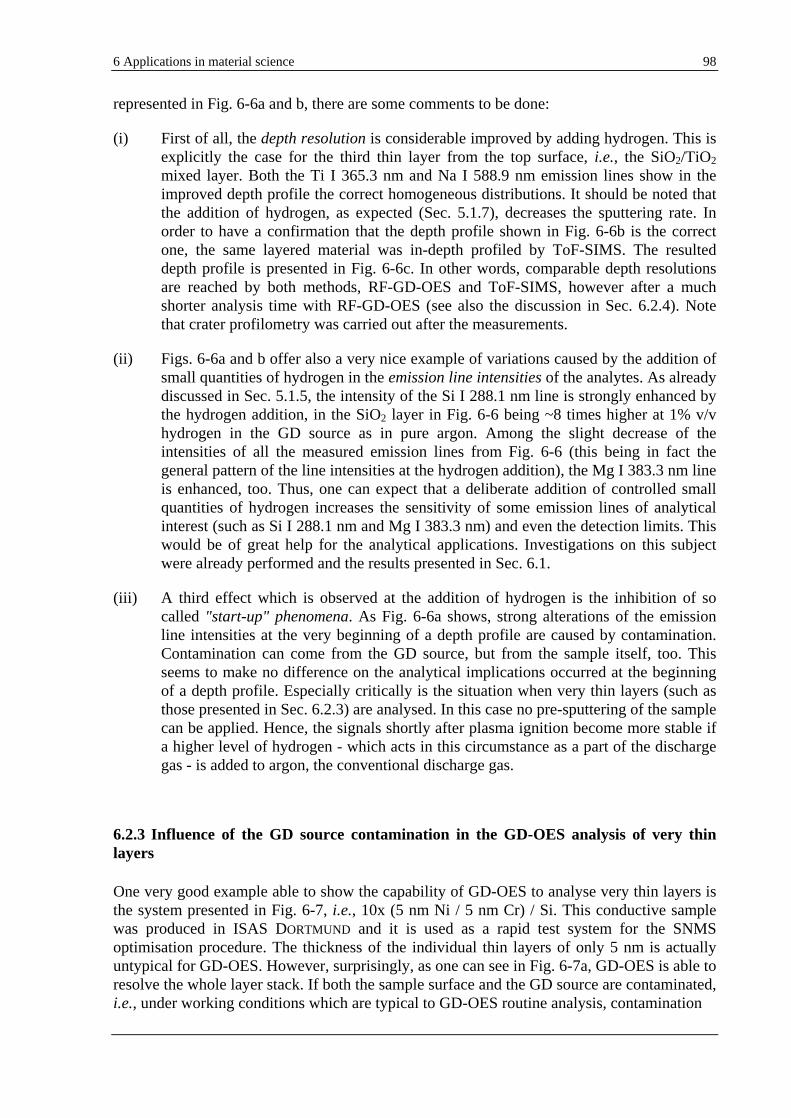
6 Applications in material science 98
represented in Fig. 6-6a and b, there are some comments to be done:
(i) First of all, the depth resolution is considerable improved by adding hydrogen. This is explicitly the case for the third thin layer from the top surface, i.e., the SiO2/TiO2
mixed layer. Both the Ti I 365.3 nm and Na I 588.9 nm emission lines show in the improved depth profile the correct homogeneous distributions. It should be noted that the addition of hydrogen, as expected (Sec. 5.1.7), decreases the sputtering rate. In order to have a confirmation that the depth profile shown in Fig. 6-6b is the correct one, the same layered material was in-depth profiled by ToF-SIMS. The resulted depth profile is presented in Fig. 6-6c. In other words, comparable depth resolutions are reached by both methods, RF-GD-OES and ToF-SIMS, however after a much shorter analysis time with RF-GD-OES (see also the discussion in Sec. 6.2.4). Note that crater profilometry was carried out after the measurements.
(ii) Figs. 6-6a and b offer also a very nice example of variations caused by the addition of small quantities of hydrogen in the emission line intensities of the analytes. As already discussed in Sec. 5.1.5, the intensity of the Si I 288.1 nm line is strongly enhanced by the hydrogen addition, in the SiO2 layer in Fig. 6-6 being ~8 times higher at 1% v/v hydrogen in the GD source as in pure argon. Among the slight decrease of the intensities of all the measured emission lines from Fig. 6-6 (this being in fact the general pattern of the line intensities at the hydrogen addition), the Mg I 383.3 nm line is enhanced, too. Thus, one can expect that a deliberate addition of controlled small quantities of hydrogen increases the sensitivity of some emission lines of analytical interest (such as Si I 288.1 nm and Mg I 383.3 nm) and even the detection limits. This would be of great help for the analytical applications. Investigations on this subject were already performed and the results presented in Sec. 6.1.
(iii) A third effect which is observed at the addition of hydrogen is the inhibition of so called "start-up" phenomena. As Fig. 6-6a shows, strong alterations of the emission line intensities at the very beginning of a depth profile are caused by contamination. Contamination can come from the GD source, but from the sample itself, too. This seems to make no difference on the analytical implications occurred at the beginning of a depth profile. Especially critically is the situation when very thin layers (such as those presented in Sec. 6.2.3) are analysed. In this case no pre-sputtering of the sample can be applied. Hence, the signals shortly after plasma ignition become more stable if a higher level of hydrogen - which acts in this circumstance as a part of the discharge gas - is added to argon, the conventional discharge gas.
6.2.3 Influence of the GD source contamination in the GD-OES analysis of very thin layers
One very good example able to show the capability of GD-OES to analyse very thin layers is the system presented in Fig. 6-7, i.e., 10x (5 nm Ni / 5 nm Cr) / Si. This conductive sample was produced in ISAS DORTMUND and it is used as a rapid test system for the SNMS optimisation procedure. The thickness of the individual thin layers of only 5 nm is actually untypical for GD-OES. However, surprisingly, as one can see in Fig. 6-7a, GD-OES is able to resolve the whole layer stack. If both the sample surface and the GD source are contaminated, i.e., under working conditions which are typical to GD-OES routine analysis, contamination
6 Applications in material science 99
signals such as H, C, O, N are present at the beginning of the depth profile in Fig. 6-7a. Based on the observations presented in Sec. 2.2, one can suspect that the high intensities of the light elements at the beginning of the depth profile, mainly hydrogen, might be responsible for the alterations of the analyte signals (strong increases of the Ni I 349.2 and Cr I 425.4 nm). Therefore, it is expected that the features of the depth profile in Fig. 6-7a can be improved, if the level of contamination is reduced as low as possible. Indeed, after a thorough cleaning of
Fig. 6-7: GD-OES qualitative depth profiles of a very thin multilayers structure 10x (5 nm Ni / 5 nm Cr)
/ Si: (a) in a contaminated GD source and (b) in a clean GD source with (c) the corresponding quantified depth profile. Vdc= 700 V and Idc= 15 mA; GD source anode diameter = 4 mm. Measured emission lines: Ni I 349.2 nm; Cr I 425.4 nm; Si I 288.1 nm; H I 121.5 nm; C I 156.1 nm, and O I 130.2 nm. (d) HFM plasma SNMS optimised depth profile of the same material. UHFM= 340 V, v= 800 kHz, = 80%; mask diameter= 3 mm; measured masses 59Ni0; 52Cr0; 28Si0.
0 1 2 3 4 50
5
10
(a)
5 nm
N
O
Si
CH
Cr
Ni
In
ten
sity
(a
. u
.)
Sputtering time /s
0 1 2 3 4 50
5
10
(b)
N
O
C
H
SiCr
Ni
Inte
nsi
ty (
a.
u.)
Sputtering time /s
0 100 200 300 400 5000
1000
2000
3000
4000
(d)
SiCr
Ni
Inte
nsi
ty (
cps)
Sputtering time /s
0 50 100 1500
20
40
60
80
100
(c) Si
CrNi
Co
nce
ntr
atio
n (w
t-%
)
Depth /nm
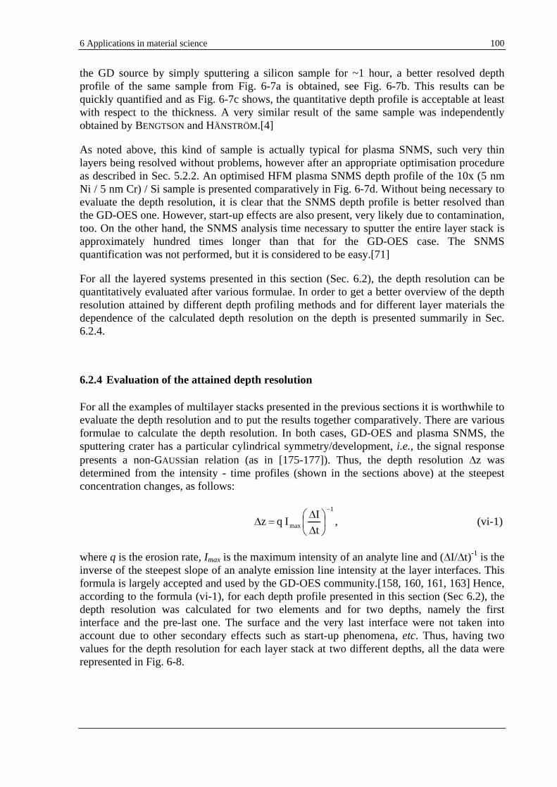
6 Applications in material science 100
the GD source by simply sputtering a silicon sample for ~1 hour, a better resolved depth profile of the same sample from Fig. 6-7a is obtained, see Fig. 6-7b. This results can be quickly quantified and as Fig. 6-7c shows, the quantitative depth profile is acceptable at least with respect to the thickness. A very similar result of the same sample was independently obtained by BENGTSON and HÄNSTRÖM.[4]
As noted above, this kind of sample is actually typical for plasma SNMS, such very thin layers being resolved without problems, however after an appropriate optimisation procedure as described in Sec. 5.2.2. An optimised HFM plasma SNMS depth profile of the 10x (5 nm Ni / 5 nm Cr) / Si sample is presented comparatively in Fig. 6-7d. Without being necessary to evaluate the depth resolution, it is clear that the SNMS depth profile is better resolved than the GD-OES one. However, start-up effects are also present, very likely due to contamination, too. On the other hand, the SNMS analysis time necessary to sputter the entire layer stack is approximately hundred times longer than that for the GD-OES case. The SNMS quantification was not performed, but it is considered to be easy.[71]
For all the layered systems presented in this section (Sec. 6.2), the depth resolution can be quantitatively evaluated after various formulae. In order to get a better overview of the depth resolution attained by different depth profiling methods and for different layer materials the dependence of the calculated depth resolution on the depth is presented summarily in Sec. 6.2.4.
6.2.4 Evaluation of the attained depth resolution
For all the examples of multilayer stacks presented in the previous sections it is worthwhile to evaluate the depth resolution and to put the results together comparatively. There are various formulae to calculate the depth resolution. In both cases, GD-OES and plasma SNMS, the sputtering crater has a particular cylindrical symmetry/development, i.e., the signal response presents a non-GAUSSian relation (as in [175-177]). Thus, the depth resolution z was determined from the intensity - time profiles (shown in the sections above) at the steepest concentration changes, as follows:
1
max t
II q z , (vi-1)
where q is the erosion rate, Imax is the maximum intensity of an analyte line and ( / t)-1 is the inverse of the steepest slope of an analyte emission line intensity at the layer interfaces. This formula is largely accepted and used by the GD-OES community.[158, 160, 161, 163] Hence, according to the formula (vi-1), for each depth profile presented in this section (Sec 6.2), the depth resolution was calculated for two elements and for two depths, namely the first interface and the pre-last one. The surface and the very last interface were not taken into account due to other secondary effects such as start-up phenomena, etc. Thus, having two values for the depth resolution for each layer stack at two different depths, all the data were represented in Fig. 6-8.
6 Applications in material science 101
As one can see in the legend of Fig. 6-8, the calculated depth resolution is shown for all the multilayer structures in the same succession as presented along the Sec. 6.2. The depth resolution attained by ToF-SIMS, found as low as 40-50 nm and not varying with the thickness, due to the different criterion of calculation, is not included in Fig. 6-8. The clear messages provided by Fig. 6-8 are: (i) the attained depth resolution is proportional to the depth; (ii) the values reached with HFM plasma SNMS (from 5 nm at the near surface region up to ~40 nm at a depth of 900 nm) are better than those reached with RF-GD-OES (ranging from ~5 nm in the near surface up to ~60 nm at 900 nm), and (iii) not to see directly from this figure, but observed in all the depth profiles above, due to the very high sputtering rates (~100 times higher than those in plasma SNMS), the prospected depth is much higher in GD-OES. Note that better performances are expected in the near future from RF-GD-OES, the present rf-technique limiting strongly the obtained results. Adding the ToF-SIMS data, the following overviewing table sums up comparatively the most relevant features resulted from the experiments above:
Table 6-1: Comparison of some relevant features of the analytical methods used for investigating of electrically non-conductive layered materials (++: very well, +: well)
RF-GDOES HFM plasma SNMS ToF-SIMS
Depth resolution + ++
Analysis time ++
Maximal depth ++
Detection of alkali diffusion ++
Fig. 6-8: General picture of the depth resolution attained for the optimised RF-GD-OES and HFM plasma SNMS depth profiles of the multilayer materials presented in Sec. 6.2 in dependence on the depth. Depth resolution is calculated corresponding to formula (vi-1); red lines: RF-GD-OES; black lines: HFM plasma SNMS.
0 500 1000 5000 60000
50
100
150
200
RF-GD-OESHFM plasma SNMS
(Ni/Cr)
ML
(Ni/Cr)
ML
(CrAlN/CrN)
ML
(SiO
2/TiO
2)
ML 1mm
(SiO
2/TiO
2)
ML 1mm
(SiO
2/TiO
2)
ML 3mm
(SiO
2/TiO
2)
ML 3mm
(Si
3N
4/SiO
2)
ML
(Si
3N
4/SiO
2)
ML D
ep
th r
eso
ltutio
n (
z) /
nm
Depth (z) /nm
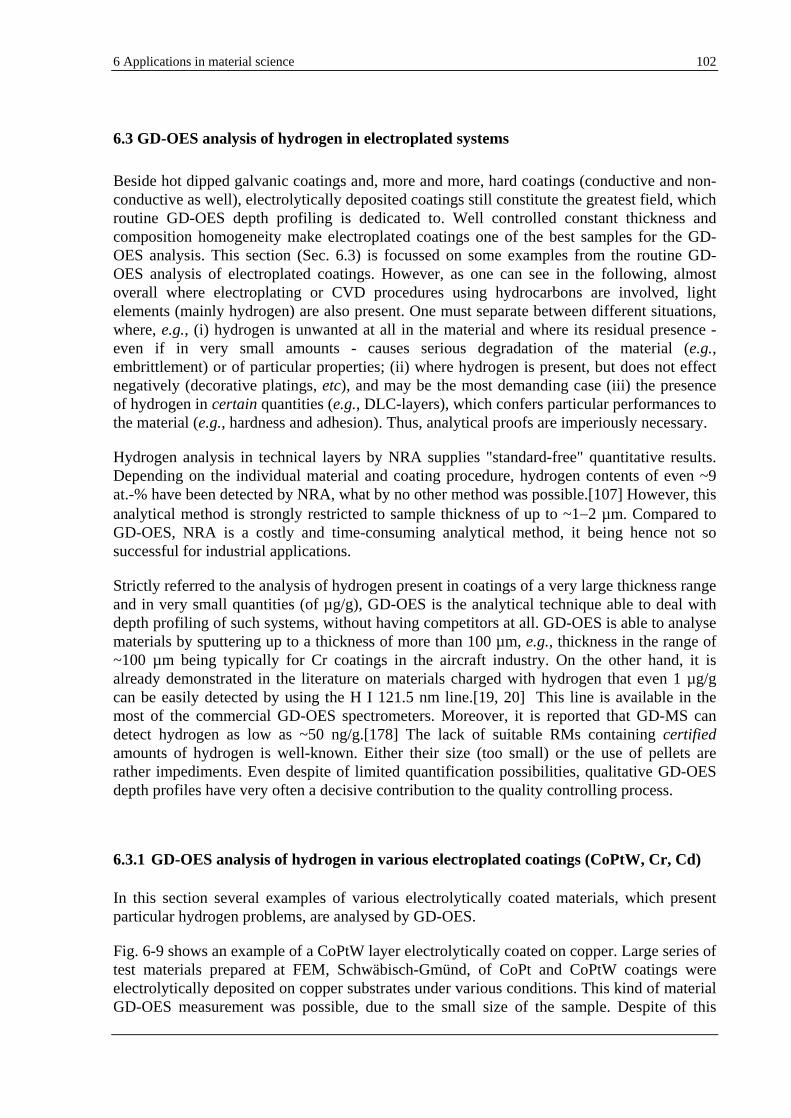
6 Applications in material science 102
6.3 GD-OES analysis of hydrogen in electroplated systems
Beside hot dipped galvanic coatings and, more and more, hard coatings (conductive and non-conductive as well), electrolytically deposited coatings still constitute the greatest field, which routine GD-OES depth profiling is dedicated to. Well controlled constant thickness and composition homogeneity make electroplated coatings one of the best samples for the GD-OES analysis. This section (Sec. 6.3) is focussed on some examples from the routine GD-OES analysis of electroplated coatings. However, as one can see in the following, almost overall where electroplating or CVD procedures using hydrocarbons are involved, light elements (mainly hydrogen) are also present. One must separate between different situations, where, e.g., (i) hydrogen is unwanted at all in the material and where its residual presence - even if in very small amounts - causes serious degradation of the material (e.g., embrittlement) or of particular properties; (ii) where hydrogen is present, but does not effect negatively (decorative platings, etc), and may be the most demanding case (iii) the presence of hydrogen in certain quantities (e.g., DLC-layers), which confers particular performances to the material (e.g., hardness and adhesion). Thus, analytical proofs are imperiously necessary.
Hydrogen analysis in technical layers by NRA supplies "standard-free" quantitative results. Depending on the individual material and coating procedure, hydrogen contents of even ~9 at.-% have been detected by NRA, what by no other method was possible.[107] However, this analytical method is strongly restricted to sample thickness of up to ~1 2 µm. Compared to GD-OES, NRA is a costly and time-consuming analytical method, it being hence not so successful for industrial applications.
Strictly referred to the analysis of hydrogen present in coatings of a very large thickness range and in very small quantities (of µg/g), GD-OES is the analytical technique able to deal with depth profiling of such systems, without having competitors at all. GD-OES is able to analyse materials by sputtering up to a thickness of more than 100 µm, e.g., thickness in the range of ~100 µm being typically for Cr coatings in the aircraft industry. On the other hand, it is already demonstrated in the literature on materials charged with hydrogen that even 1 µg/g can be easily detected by using the H I 121.5 nm line.[19, 20] This line is available in the most of the commercial GD-OES spectrometers. Moreover, it is reported that GD-MS can detect hydrogen as low as ~50 ng/g.[178] The lack of suitable RMs containing certified amounts of hydrogen is well-known. Either their size (too small) or the use of pellets are rather impediments. Even despite of limited quantification possibilities, qualitative GD-OES depth profiles have very often a decisive contribution to the quality controlling process.
6.3.1 GD-OES analysis of hydrogen in various electroplated coatings (CoPtW, Cr, Cd)
In this section several examples of various electrolytically coated materials, which present particular hydrogen problems, are analysed by GD-OES.
Fig. 6-9 shows an example of a CoPtW layer electrolytically coated on copper. Large series of test materials prepared at FEM, Schwäbisch-Gmünd, of CoPt and CoPtW coatings were electrolytically deposited on copper substrates under various conditions. This kind of material GD-OES measurement was possible, due to the small size of the sample. Despite of this
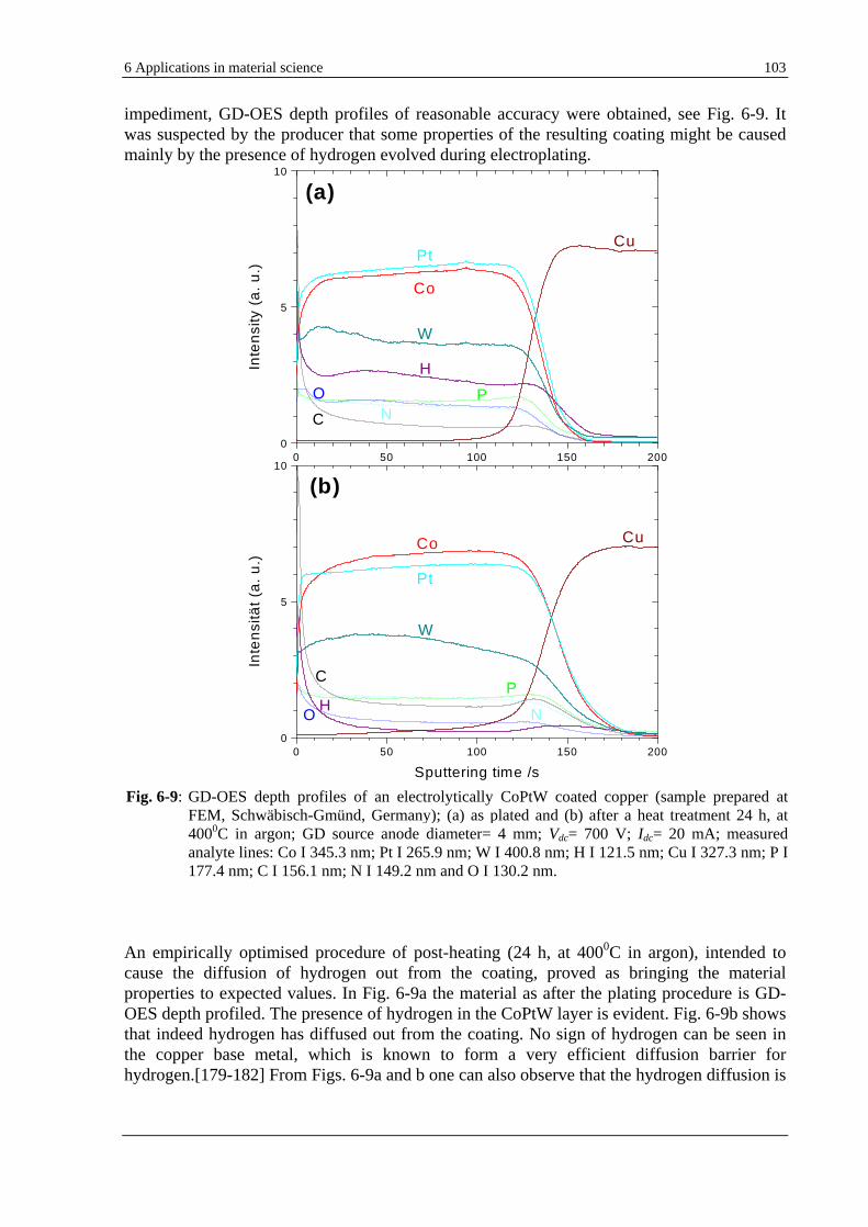
6 Applications in material science 103
impediment, GD-OES depth profiles of reasonable accuracy were obtained, see Fig. 6-9. It was suspected by the producer that some properties of the resulting coating might be caused mainly by the presence of hydrogen evolved during electroplating.
An empirically optimised procedure of post-heating (24 h, at 4000C in argon), intended to cause the diffusion of hydrogen out from the coating, proved as bringing the material properties to expected values. In Fig. 6-9a the material as after the plating procedure is GD-OES depth profiled. The presence of hydrogen in the CoPtW layer is evident. Fig. 6-9b shows that indeed hydrogen has diffused out from the coating. No sign of hydrogen can be seen in the copper base metal, which is known to form a very efficient diffusion barrier for hydrogen.[179-182] From Figs. 6-9a and b one can also observe that the hydrogen diffusion is
Fig. 6-9: GD-OES depth profiles of an electrolytically CoPtW coated copper (sample prepared
at FEM, Schwäbisch-Gmünd, Germany); (a) as plated and (b) after a heat treatment 24 h, at 4000C in argon; GD source anode diameter= 4 mm; Vdc= 700 V; Idc= 20 mA; measured analyte lines: Co I 345.3 nm; Pt I 265.9 nm; W I 400.8 nm; H I 121.5 nm; Cu I 327.3 nm; P I 177.4 nm; C I 156.1 nm; N I 149.2 nm and O I 130.2 nm.
0 50 100 150 2000
5
10
NPO
C
H
W
CuPt
Co
(a)
Inte
nsi
ty (
a.
u.)
0 50 100 150 2000
5
10
P
N
C
HO
W
CuCo
Pt
(b)
Inte
nsi
tät
(a.
u.)
Sputtering time /s
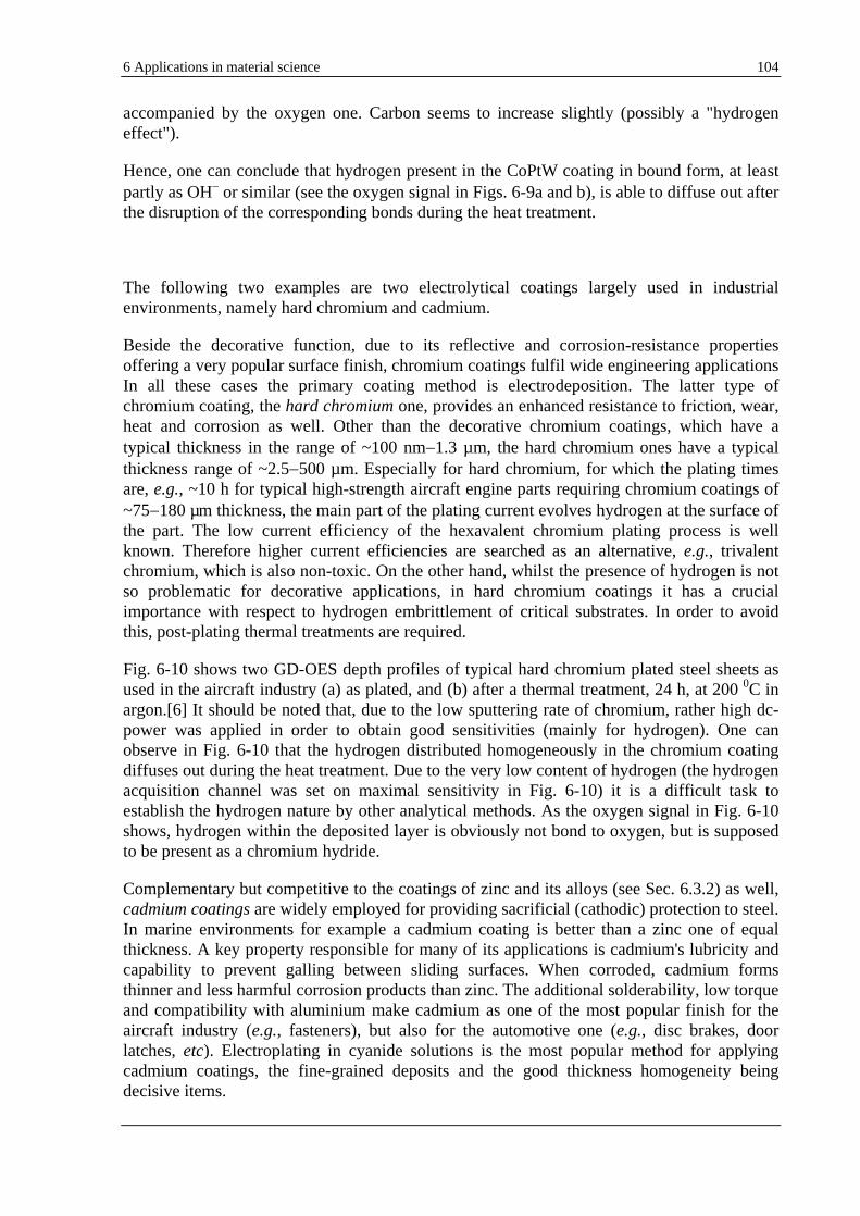
6 Applications in material science 104
accompanied by the oxygen one. Carbon seems to increase slightly (possibly a "hydrogen effect").
Hence, one can conclude that hydrogen present in the CoPtW coating in bound form, at least partly as OH or similar (see the oxygen signal in Figs. 6-9a and b), is able to diffuse out after the disruption of the corresponding bonds during the heat treatment.
The following two examples are two electrolytical coatings largely used in industrial environments, namely hard chromium and cadmium.
Beside the decorative function, due to its reflective and corrosion-resistance properties offering a very popular surface finish, chromium coatings fulfil wide engineering applications In all these cases the primary coating method is electrodeposition. The latter type of chromium coating, the hard chromium one, provides an enhanced resistance to friction, wear, heat and corrosion as well. Other than the decorative chromium coatings, which have a typical thickness in the range of ~100 nm 1.3 µm, the hard chromium ones have a typical thickness range of ~2.5 500 µm. Especially for hard chromium, for which the plating times are, e.g., ~10 h for typical high-strength aircraft engine parts requiring chromium coatings of ~75 180 µm thickness, the main part of the plating current evolves hydrogen at the surface of the part. The low current efficiency of the hexavalent chromium plating process is well known. Therefore higher current efficiencies are searched as an alternative, e.g., trivalent chromium, which is also non-toxic. On the other hand, whilst the presence of hydrogen is not so problematic for decorative applications, in hard chromium coatings it has a crucial importance with respect to hydrogen embrittlement of critical substrates. In order to avoid this, post-plating thermal treatments are required.
Fig. 6-10 shows two GD-OES depth profiles of typical hard chromium plated steel sheets as used in the aircraft industry (a) as plated, and (b) after a thermal treatment, 24 h, at 200 0C in argon.[6] It should be noted that, due to the low sputtering rate of chromium, rather high dc-power was applied in order to obtain good sensitivities (mainly for hydrogen). One can observe in Fig. 6-10 that the hydrogen distributed homogeneously in the chromium coating diffuses out during the heat treatment. Due to the very low content of hydrogen (the hydrogen acquisition channel was set on maximal sensitivity in Fig. 6-10) it is a difficult task to establish the hydrogen nature by other analytical methods. As the oxygen signal in Fig. 6-10 shows, hydrogen within the deposited layer is obviously not bond to oxygen, but is supposed to be present as a chromium hydride.
Complementary but competitive to the coatings of zinc and its alloys (see Sec. 6.3.2) as well, cadmium coatings are widely employed for providing sacrificial (cathodic) protection to steel. In marine environments for example a cadmium coating is better than a zinc one of equal thickness. A key property responsible for many of its applications is cadmium's lubricity and capability to prevent galling between sliding surfaces. When corroded, cadmium forms thinner and less harmful corrosion products than zinc. The additional solderability, low torque and compatibility with aluminium make cadmium as one of the most popular finish for the aircraft industry (e.g., fasteners), but also for the automotive one (e.g., disc brakes, door latches, etc). Electroplating in cyanide solutions is the most popular method for applying cadmium coatings, the fine-grained deposits and the good thickness homogeneity being decisive items.
6 Applications in material science 105
Hydrogen embrittlement is unfortunately typically for this type of electrolytical coatings, too. Heat treatments procedures applied after the plating are in this case also necessary to avoid/reduce the risk of embrittlement by driving out the hydrogen evolved during plating and present in material. Fig. 6-11 shows two GD-OES depth profiles of real samples used in the aircraft industry (samples offered to investigations by generosity of LUFTHANSA, Hamburg, Germany): (a) as plated and (b) after a heat treatment.[6, 179-181] It should be noted that this kind of samples, in their usual form, are rather improper to GD-OES analysis, the sample surface being very rough and powdery as well. The samples were able to be in-depth profiled by GD-OES. However rather high signals of nitrogen and oxygen were observed and basic pressures higher than normal were attained. Of these both impediments it was got rid successfully by pressing the coated sheets at an appropriate pressure (10 kt). As one can see in Fig. 6-11, after a necessary optimisation procedure in terms of depth resolution, hydrogen is present (i) in the coating, very likely mainly as contamination from
Fig. 6-10: GD-OES depth profiles
of a typical hard chromium coating electrolytically deposited on steel (sample prepared by LUFTHANSA, Hamburg, Germany); (a) as plated and (b) after a heat treatment 24h, at 2000C in argon; GD source anode diameter= 4 mm; Vdc= 900 V; Idc= 30 mA; measured analyte lines: Cr I 425.4 nm; Fe I 371.9 nm; H I 121.5 nm; C I 156.1 nm; N I 149.2 nm and O I 130.2 nm.
0 500 1000 1500 20000
5
10
(a)
O NC
H
FeCr
Inte
nsi
ty (
a.
u.)
0 500 1000 15000
5
10
(b)
O
H
N C
FeCr
Inte
nsity
(a. u
.)
Sputtering time /s
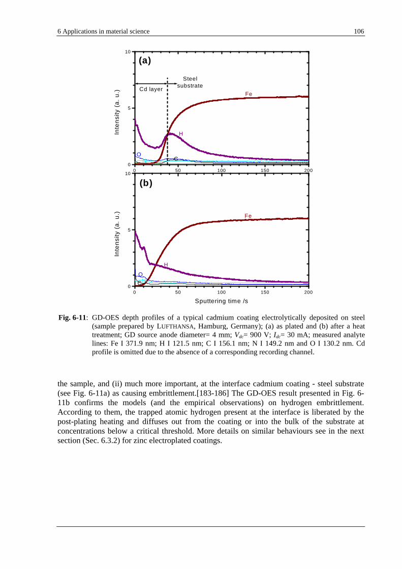
6 Applications in material science 106
the sample, and (ii) much more important, at the interface cadmium coating - steel substrate (see Fig. 6-11a) as causing embrittlement.[183-186] The GD-OES result presented in Fig. 6-11b confirms the models (and the empirical observations) on hydrogen embrittlement. According to them, the trapped atomic hydrogen present at the interface is liberated by the post-plating heating and diffuses out from the coating or into the bulk of the substrate at concentrations below a critical threshold. More details on similar behaviours see in the next section (Sec. 6.3.2) for zinc electroplated coatings.
Fig. 6-11: GD-OES depth profiles of a typical cadmium coating electrolytically deposited on steel (sample prepared by LUFTHANSA, Hamburg, Germany); (a) as plated and (b) after a heat treatment; GD source anode diameter= 4 mm; Vdc= 900 V; Idc= 30 mA; measured analyte lines: Fe I 371.9 nm; H I 121.5 nm; C I 156.1 nm; N I 149.2 nm and O I 130.2 nm. Cd profile is omitted due to the absence of a corresponding recording channel.
0 50 100 150 2000
5
10
(a)
Cd layer
Steelsubstrate
NO
C
H
Fe
Inte
nsi
ty (
a.
u.)
0 50 100 150 2000
5
10
(b)
NO
C
H
Fe
Inte
nsi
ty (
a.
u.)
Sputtering time /s
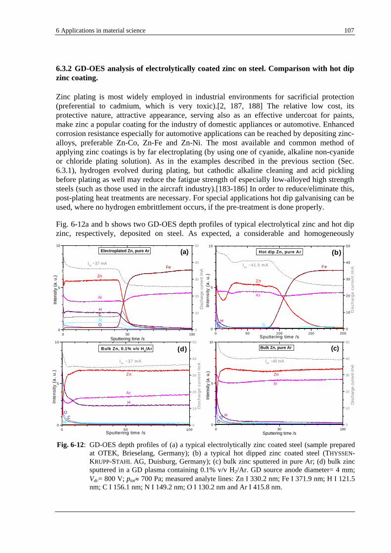
6 Applications in material science 107
6.3.2 GD-OES analysis of electrolytically coated zinc on steel. Comparison with hot dip zinc coating.
Zinc plating is most widely employed in industrial environments for sacrificial protection (preferential to cadmium, which is very toxic).[2, 187, 188] The relative low cost, its protective nature, attractive appearance, serving also as an effective undercoat for paints, make zinc a popular coating for the industry of domestic appliances or automotive. Enhanced corrosion resistance especially for automotive applications can be reached by depositing zinc-alloys, preferable Zn-Co, Zn-Fe and Zn-Ni. The most available and common method of applying zinc coatings is by far electroplating (by using one of cyanide, alkaline non-cyanide or chloride plating solution). As in the examples described in the previous section (Sec. 6.3.1), hydrogen evolved during plating, but cathodic alkaline cleaning and acid pickling before plating as well may reduce the fatigue strength of especially low-alloyed high strength steels (such as those used in the aircraft industry).[183-186] In order to reduce/eliminate this, post-plating heat treatments are necessary. For special applications hot dip galvanising can be used, where no hydrogen embrittlement occurs, if the pre-treatment is done properly.
Fig. 6-12a and b shows two GD-OES depth profiles of typical electrolytical zinc and hot dip zinc, respectively, deposited on steel. As expected, a considerable and homogeneously
Fig. 6-12: GD-OES depth profiles of (a) a typical electrolytically zinc coated steel (sample prepared at OTEK, Brieselang, Germany); (b) a typical hot dipped zinc coated steel (THYSSEN-KRUPP-STAHL AG, Duisburg, Germany); (c) bulk zinc sputtered in pure Ar; (d) bulk zinc sputtered in a GD plasma containing 0.1% v/v H2/Ar. GD source anode diameter= 4 mm; Vdc= 800 V; ptot
700 Pa; measured analyte lines: Zn I 330.2 nm; Fe I 371.9 nm; H I 121.5 nm; C I 156.1 nm; N I 149.2 nm; O I 130.2 nm and Ar I 415.8 nm.
0 50 1000
5
10
Electroplated Zn, pure Ar (a)
H
Idc ~37 mAFe
Zn
Dis
char
ge c
urre
nt /m
A
Inte
nsity
(a. u
.)
Sputtering time /s
0
10
20
30
40
50
CN
Ar
O
0 50 100 150 2000
5
10
C NOH
Ar
Fe
Zn
Inte
nsi
ty (
a.
u.)
Sputtering time /s
0
10
20
30
40
50
Hot dip Zn, pure Ar (b)
Idc
~41.5 mA
Dis
cha
rge
curr
en
t /m
A
0 50 1000
5
10
Bulk Zn, pure Ar (c)
C NO H
Ar
Zn
Inte
nsity
(a. u
.)
Sputtering time /s
0
10
20
30
40
50
Idc ~40 mA
Dis
char
ge c
urre
nt /m
A
0 50 1000
5
10
Bulk Zn, 0.1% v/v H2/Ar (d)
NC
O
H
Ar
Zn
Inte
nsi
ty (
a.
u.)
Sputtering time /s
0
10
20
30
40
50
Idc
~37 mA
Dis
cha
rge
curr
en
t /m
A
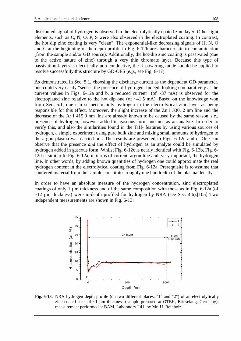
6 Applications in material science 108
distributed signal of hydrogen is observed in the electrolytically coated zinc layer. Other light elements, such as C, N, O, P, S were also observed in the electroplated coating. In contrast, the hot dip zinc coating is very "clean". The exponential-like decreasing signals of H, N, O and C at the beginning of the depth profile in Fig. 6-12b are characteristic to contamination (from the sample and/or GD source). Additionally, the hot-dip zinc coating is passivated (due to the active nature of zinc) through a very thin chromate layer. Because this type of passivation layers is electrically non-conductive, the rf-powering mode should be applied to resolve successfully this structure by GD-OES (e.g., see Fig. 6-17).
As demonstrated in Sec. 5.1, choosing the discharge current as the dependent GD-parameter, one could very easily "sense" the presence of hydrogen. Indeed, looking comparatively at the current values in Figs. 6-12a and b, a reduced current (of ~37 mA) is observed for the electroplated zinc relative to the hot dip one (of ~41.5 mA). Based on the knowledge won from Sec. 5.1, one can suspect mainly hydrogen in the electrolytical zinc layer as being responsible for this effect. Moreover, the slight increase of the Zn I 330. 2 nm line and the decrease of the Ar I 415.9 nm line are already known to be caused by the same reason, i.e., presence of hydrogen, however added in gaseous form and not as an analyte. In order to verify this, and also the similarities found in the TiH2 features by using various sources of hydrogen, a simple experiment using pure bulk zinc and mixing small amounts of hydrogen to the argon plasma was carried out. The results are presented in Figs. 6-12c and d. One can observe that the presence and the effect of hydrogen as an analyte could be simulated by hydrogen added in gaseous form. Whilst Fig. 6-12c is nearly identical with Fig. 6-12b, Fig. 6-12d is similar to Fig. 6-12a, in terms of current, argon line and, very important, the hydrogen line. In other words, by adding known quantities of hydrogen one could approximate the real hydrogen content in the electrolytical coating from Fig. 6-12a. Prerequisite is to assume that sputtered material from the sample constitutes roughly one hundredth of the plasma density.
In order to have an absolute measure of the hydrogen concentration, zinc electroplated coatings of only 1 µm thickness and of the same composition with those as in Fig. 6-12a (of ~12 µm thickness) were in-depth profiled for hydrogen by NRA (see Sec. 4.6).[105] Two independent measurements are shown in Fig. 6-13:
Fig. 6-13: NRA hydrogen depth profile (on two different
places, "1" and "2") of an electrolytically zinc coated steel of ~1 µm thickness (sample prepared at OTEK, Brieselang, Germany); measurement performed at BAM, Laboratory I.41, by Mr. U. Reinholz.
0 500 10000
5
10
15
20
25
30
35
steelsubstrate
Zn layer
1
2
H c
on
cen
tra
tion
(at.
-%)
Depth /nm
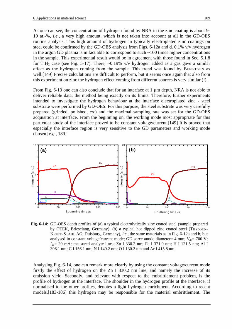
6 Applications in material science 109
As one can see, the concentration of hydrogen found by NRA in the zinc coating is about 9-10 at.-%, i.e., a very high amount, which is not taken into account at all in the GD-OES routine analysis. This high amount of hydrogen in typically electroplated zinc coatings on steel could be confirmed by the GD-OES analysis from Figs. 6-12a and d. 0.1% v/v hydrogen in the argon GD plasma is in fact able to correspond to such ~100 times higher concentrations in the sample. This experimental result would be in agreement with those found in Sec. 5.1.8 for TiH2 case (see Fig. 5-17). There, ~0.19% v/v hydrogen added as a gas gave a similar effect as the hydrogen coming from the sample. This trend was found by BENGTSON as well.[149] Precise calculations are difficult to perform, but it seems once again that also from this experiment on zinc the hydrogen effect coming from different sources is very similar (!).
From Fig. 6-13 one can also conclude that for an interface at 1 µm depth, NRA is not able to deliver reliable data, the method being exactly on its limits. Therefore, further experiments intended to investigate the hydrogen behaviour at the interface electroplated zinc - steel substrate were performed by GD-OES. For this purpose, the steel substrate was very carefully prepared (grinded, polished, etc) and the maximal sampling rate was set for the GD-OES acquisition at interface. From the beginning on, the working mode most appropriate for this particular study of the interface proved to be constant voltage/current.[149] It is proved that especially the interface region is very sensitive to the GD parameters and working mode chosen.[e.g., 189]
Analysing Fig. 6-14, one can remark more clearly by using the constant voltage/current mode firstly the effect of hydrogen on the Zn I 330.2 nm line, and namely the increase of its emission yield. Secondly, and relevant with respect to the embrittlement problem, is the profile of hydrogen at the interface. The shoulder in the hydrogen profile at the interface, if normalised to the other profiles, denotes a light hydrogen enrichment. According to recent models,[183-186] this hydrogen may be responsible for the material embrittlement. The
Fig. 6-14: GD-OES depth profiles of (a) a typical electrolytically zinc coated steel (sample prepared by OTEK, Brieselang, Germany); (b) a typical hot dipped zinc coated steel (THYSSEN-KRUPP-STAHL AG, Duisburg, Germany), i.e., the same materials as in Fig. 6-12a and b, but analysed in constant voltage/current mode; GD sorce anode diameter= 4 mm; Vdc= 700 V; Idc= 20 mA; measured analyte lines: Zn I 330.2 nm; Fe I 371.9 nm; H I 121.5 nm; Al I 396.1 nm; C I 156.1 nm; N I 149.2 nm; O I 130.2 nm and Ar I 415.8 nm.
0 50 100 150 2000
5
10
O N
C
H
FeZn
(a)
Inte
nsi
ty (
a.
u.)
Sputtering time /s
0 50 100 150 2000
5
10
HAl
Fe
Zn
(b)
Inte
nsi
ty (
a.
u.)
Sputtering time /s
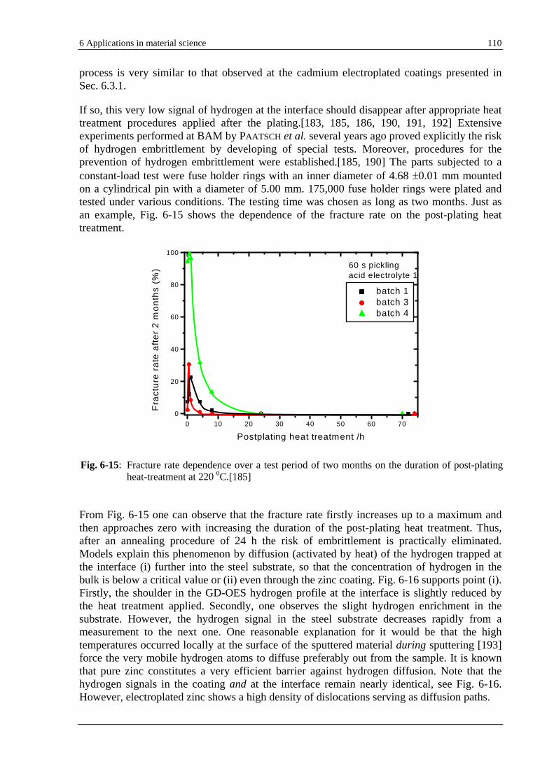
6 Applications in material science 110
process is very similar to that observed at the cadmium electroplated coatings presented in Sec. 6.3.1.
If so, this very low signal of hydrogen at the interface should disappear after appropriate heat treatment procedures applied after the plating.[183, 185, 186, 190, 191, 192] Extensive experiments performed at BAM by PAATSCH et al. several years ago proved explicitly the risk of hydrogen embrittlement by developing of special tests. Moreover, procedures for the prevention of hydrogen embrittlement were established.[185, 190] The parts subjected to a constant-load test were fuse holder rings with an inner diameter of 4.68 0.01 mm mounted on a cylindrical pin with a diameter of 5.00 mm. 175,000 fuse holder rings were plated and tested under various conditions. The testing time was chosen as long as two months. Just as an example, Fig. 6-15 shows the dependence of the fracture rate on the post-plating heat treatment.
From Fig. 6-15 one can observe that the fracture rate firstly increases up to a maximum and then approaches zero with increasing the duration of the post-plating heat treatment. Thus, after an annealing procedure of 24 h the risk of embrittlement is practically eliminated. Models explain this phenomenon by diffusion (activated by heat) of the hydrogen trapped at the interface (i) further into the steel substrate, so that the concentration of hydrogen in the bulk is below a critical value or (ii) even through the zinc coating. Fig. 6-16 supports point (i). Firstly, the shoulder in the GD-OES hydrogen profile at the interface is slightly reduced by the heat treatment applied. Secondly, one observes the slight hydrogen enrichment in the substrate. However, the hydrogen signal in the steel substrate decreases rapidly from a measurement to the next one. One reasonable explanation for it would be that the high temperatures occurred locally at the surface of the sputtered material during sputtering [193] force the very mobile hydrogen atoms to diffuse preferably out from the sample. It is known that pure zinc constitutes a very efficient barrier against hydrogen diffusion. Note that the hydrogen signals in the coating and at the interface remain nearly identical, see Fig. 6-16. However, electroplated zinc shows a high density of dislocations serving as diffusion paths.
Fig. 6-15: Fracture rate dependence over a test period of two months on the duration of post-plating heat-treatment at 220 0C.[185]
0 10 20 30 40 50 60 70
0
20
40
60
80
100
60 s picklingacid electrolyte 1
batch 1
batch 3
batch 4
Fra
ctu
re r
ate
aft
er
2 m
on
ths
(%)
Postplating heat treatment /h
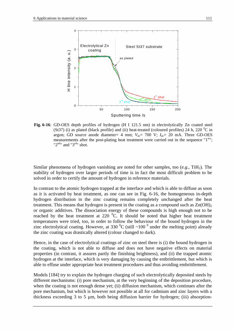
6 Applications in material science 111
Similar phenomena of hydrogen vanishing are noted for other samples, too (e.g., TiH2). The stability of hydrogen over larger periods of time is in fact the most difficult problem to be solved in order to certify the amount of hydrogen in reference materials.
In contrast to the atomic hydrogen trapped at the interface and which is able to diffuse as soon as it is activated by heat treatment, as one can see in Fig. 6-16, the homogeneous in-depth hydrogen distribution in the zinc coating remains completely unchanged after the heat treatment. This means that hydrogen is present in the coating as a compound such as Zn(OH)2
or organic additives. The dissociation energy of these compounds is high enough not to be reached by the heat treatment at 220 0C. It should be noted that higher heat treatment temperatures were tried, too, in order to follow the behaviour of the bound hydrogen in the zinc electrolytical coating. However, at 330 0C (still ~100 0 under the melting point) already the zinc coating was drastically altered (colour changed to dark).
Hence, in the case of electrolytical coatings of zinc on steel there is (i) the bound hydrogen in the coating, which is not able to diffuse and does not have negative effects on material properties (in contrast, it assures partly the finishing brightness), and (ii) the trapped atomic hydrogen at the interface, which is very damaging by causing the embrittlement, but which is able to effuse under appropriate heat treatment procedures and thus avoiding embrittlement.
Models [184] try to explain the hydrogen charging of such electrolytically deposited steels by different mechanisms: (i) pore mechanism, at the very beginning of the deposition procedure, when the coating is not enough dense yet; (ii) diffusion mechanism, which continues after the pore mechanism, but which is however not possible at all for cadmium and zinc layers with a thickness exceeding 3 to 5 µm, both being diffusion barrier for hydrogen; (iii) absorption-
Fig. 6-16: GD-OES depth profiles of hydrogen (H I 121.5 nm) in electrolytically Zn coated steel (St37) (i) as plated (black profile) and (ii) heat-treated (coloured profiles) 24 h, 220 0C in argon; GD source anode diameter= 4 mm; Vdc= 700 V; Idc= 20 mA. Three GD-OES measurements after the post-plating heat treatment were carried out in the sequence "1st"; "2nd" and "3rd" shot.
50 100 150 2000
1
2
3
4
Steel St37 substrateElectrolytical Zn
coating
as plated
3rd shot2nd shot
1st shot
H l
ine
inte
nsi
ty (
a.
u.)
Sputtering time /s
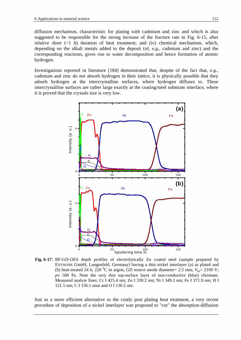
6 Applications in material science 112
diffusion mechanism, characteristic for plating with cadmium and zinc and which is also suggested to be responsible for the strong increase of the fracture rate in Fig. 6-15, after relative short (~1 h) duration of heat treatment; and (iv) chemical mechanism, which, depending on the alkali metals added to the deposit (of, e.g., cadmium and zinc) and the corresponding reactions, gives rise to water decomposition and hence formation of atomic hydrogen.
Investigations reported in literature [184] demonstrated that, despite of the fact that, e.g., cadmium and zinc do not absorb hydrogen in their lattice, it is physically possible that they adsorb hydrogen at the intercrystalline surfaces, where hydrogen diffuses to. These intercrystalline surfaces are rather large exactly at the coating/steel substrate interface, where it is proved that the crystals size is very low.
Just as a more efficient alternative to the costly post plating heat treatment, a very recent procedure of deposition of a nickel interlayer was proposed to "cut" the absorption-diffusion
Fig. 6-17: RF-GD-OES depth profiles of electrolytically Zn coated steel (sample prepared by ENTHONE GMBH, Langenfeld, Germany) having a thin nickel interlayer (a) as plated and (b) heat-treated 24 h, 220 0C in argon; GD source anode diameter= 2.5 mm; Vpp= 2100 V; p
500 Pa. Note the very thin top-surface layer of non-conductive (blue) chromate. Measured analyte lines: Cr I 425.4 nm; Zn I 330.2 nm; Ni I 349.2 nm; Fe I 371.9 nm; H I 121.5 nm; C I 156.1 nmn and O I 130.2 nm.
0 50 100 1500
5
(a)Cr
O
C
H
Zn Ni Fe
Inte
nsi
ty (
a.
u.)
0 50 100 1500
5
(b)
OS
Cr
CH
Zn FeNi
Inte
nsi
ty (
a.
u.)
Sputtering time /s
6 Applications in material science 113
phenomena of the hydrogen trapped at the zinc/steel substrate interface.[186, 194] Fig. 6-17 shows RF-GD-OES depth profiles of such test samples. No indication of hydrogen in the steel substrate and at the interface nickel-steel substrate as well could be found neither before nor after a heat treatment procedure (Fig. 6-17b). This suggests that the new interface zinc/nickel suppresses the phenomena originating hydrogen embrittlement.
The results reported in this section show how GD-OES, as the only analytical method able to deal with hydrogen depth profiling over very thick coatings, can contribute to the control of such damaging phenomena as hydrogen embrittlement. Its consequences are much more devastating than, e.g., corrosion. The GD-OES results reported here are the very first ones published with this respect, not yet fully quantitative. Nevertheless, at least qualitatively, they confirm the existing models. Further involvement of other laboratories in investigating such a sensible field would be welcome.
7 Conclusions 114
7 Conclusions
As already stated in "Objectives", two main fields have been extensively investigated in this work by using GD-OES: (i) the multiple effect of hydrogen on emission line intensities, emission yields, sputtering rate, sputtering crater shape and GD parameters; (ii) depth profiling of layered materials, in particular thick coatings containing hydrogen and optimisation of thin multilayer non-conductive materials.
With respect to point (i) firstly fundamental investigations have been carried out (Sec. 5.1) in order to understand better or at all the elementary mechanisms of excitation and ionisation taking place in the GD plasma and actually causing the hydrogen effect when small quantities of hydrogen are present. The alternative use of neon instead of the conventional discharge gas argon or additional GD-MS measurements have been proved to be very useful in this attempt. Due to the complexity in the behaviour of the line intensities at the hydrogen addition, the relative simple and well-known emission spectra of copper, beside those of the noble carrier gas, have been thoroughly investigated (Sec. 5.1.1 and 5.1.2). Depending on the excitation energy of the emission lines, individual decreases (even down to almost vanishing of certain lines) in general, but enhancements as well of line intensities of analytes in particular have been observed. The comprehension of the (partial) energy diagrams of the noble carrier gas and hydrogen to that of the analyte gives definitely a very useful overview on the main processes. E.g., one of the key points in the understanding of the hydrogen effect is the observation of an emission continuum in the spectral range of ~220 440 nm (Sec. 5.1.3) already at hydrogen concentrations of ~0.1% v/v in the GD plasma. Being excited at an energy very close to that of the argon metastables, 11.55 and 11.72 eV, respectively, the hydrogen continuum proves the decisive role of the argon metastables (directly and efficiently quenched by hydrogen) in the GD. Consequently, a series of secondary linked occurrences are explained, e.g., the decrease of the density of the argon ions or the quenching of the Cu II lines excited at 8.23 8.78 eV above the first ionisation potential of copper. For a fuller understanding of the changes in the emission lines intensity, e.g., of the Cu I lines or the Si I lines, further investigations are still necessary. The most experimental results obtained in the present work are more and more supported by very recent work of modellers.[117, 136] Nevertheless, the extension of the models to the high current regime is also necessary.
Thinking on GD-OES analysis of materials containing hydrogen, it becomes decisive to interpret correctly the measured depth profiles, i.e., (i) the hydrogen itself, and (ii) the other (affected) analytical lines, too. On the other hand, knowing the emission lines providing enhanced emission yields under the hydrogen influence, it was proved (Sec. 6.1) that the controlled addition of hydrogen improves relevant analytical figures of merit such as sensitivity of detection for certain elements (such as Mg, Si, Cu), and even the detection limits.
Common emission lines of analytes have been investigated under the influence of hydrogen added as a gas up to 0.1% v/v into an argon GD plasma (Sec. 5.1.5). Based on the results in this concentration range, i.e., corresponding approximately to the whole concentration range of hydrogen in the sample, PAYLING et al. have proposed an algorithm for the correction of the alterations in the emission lines intensities caused by hydrogen. So, whilst part of the hydrogen effect (the change in the emission lines intensity) seems to be possible to be
7 Conclusions 115
corrected for, the quantification of the hydrogen itself remains unsolved yet and this due to the lack of suitable CRMs containing hydrogen. Nevertheless, by using of materials containing hydrogen (stable at least temporary), it is demonstrated that the hydrogen effect seems to be nearly the same with respect to various aspects (the dependent GD parameter, hydrogen emission lines and continuum, noble carrier gas and analyte emission lines) independent of the source of hydrogen, i.e., as a gas and as an analyte (Sec. 5.1.8 and 6.3.2). Hence, this similarity allows the simulation of the hydrogen effect by (experimentally easily) adding defined quantities of hydrogen instead of using hydrogen as an analyte.
The presence of hydrogen in small quantities in an argon GD plasma causes the increase of the GD resistance, this meaning a decrease of the sputtering rate for the most materials investigated. More important from the analytical point of view, the sputtering crater shape is also very sensitive to the content of hydrogen in the GD plasma. In turn, knowing this facet of the hydrogen effect (Sec. 5.1.7) one could imagine experiments, where the best attainable depth resolution, sometimes limited from technical reasons, can be enhanced by the controlled addition of hydrogen. This is demonstrated on real examples of layered non-conductive materials (Sec. 6.2), for which it is well-known that the optimisation of the depth resolution is strongly limited by the maximal rf-voltage supplied by the rf-generator or by the sample properties.
Examples of systematic optimisation procedures with respect to the depth resolution are reported for thin multilayer materials (Sec. 5.2). These costly procedures have been comparatively tested by using other competitive depth profiling methods, such as plasma SNMS and SIMS. Some challenging materials (such as thin non-conductive layers on non-conductive substrates) have been deliberately selected in this experiment. Especially for non-conductive layered materials, there are certain and narrow ranges where the GD parameters to be driven give the optimal depth resolutions. However, each material (composition of the coated layers and composition and thickness of the substrate) requires its particular parameters. Classes of certain materials can be established and the trends of the sputtering crater form with the GD power and pressure should be known. A slightly worse depth resolution, but a much shorter analysis time have been evidenced for GD-OES against the other techniques (Sec. 6.2).
Depth profiling of very thin layers (5 nm a single layer) is shown to be possible not only with conventional techniques such as SNMS, but also with GD-OES. However, special cares uncommon to the routine GD-OES analysis must be taken into account. The prerequisite in GD-OES analysis of very thin layers is to keep the contamination level in the GD source to a minimum by long prior sputtering of clean materials (ideally Si). Not only the depth resolution, but the analyte line intensities are affected by contamination, which may come from the GD source and/or the sample itself, but having the same negative effect exponentially-like at the beginning of a depth profile. The basic element responsibly for contamination is hydrogen. One can explain the alteration of the depth resolution, but also the change in the emission line intensities by changes in the excitation mechanisms (as in Sec. 5.1.5), by interference with molecular bands of contamination compounds containing hydrogen (Sec. 5.1.6) and, not least, by the superposition of the hydrogen continuum. The knowledge of such particularities of the GD-OES analysis can be successfully used for very thin films analysis, the results being comparable with those obtained with SNMS (Sec. 6.2.4).
The thorough knowledge of the hydrogen effect in GDS contributes thus decisively to the correct interpretation of the GD-OES depth profiles of materials containing hydrogen and of
7 Conclusions 116
thin layers not containing hydrogen but being affected by it from contamination. The simple qualitative monitoring of the hydrogen signal often proved to be very useful. The GD-OES analysis of hydrogen itself is at least qualitatively or comparatively (good - bad samples) also possible and, due to its uniqueness, opens up new and large application fields of interest. Electroplated coatings are only one of them. There is no other analytical method which is able to analyse hydrogen in concentration ranges of µg/g at interfaces in a depth of, e.g., some tens of µm. Some materials relevant with this respect have been selected for investigations by GD-OES (Sec. 6.3).
Section 6.3.1 shows examples of materials where hydrogen in electrolytical coatings such as CoPt or CoPtW deposited on copper worsens the properties of the substrate material. GD-OES shows successfully how hydrogen is dispensed by diffusion from the coating by appropriate post-plating heat treatments. Similar behaviour is noted for other electroplated coatings such as, e.g., hard chromium. In both cases it is assumed that hydrogen in atomic form is able to diffuse out from the sample after breaking of compounds (hydride) containing hydrogen. Due to their very low content, it is very difficult (or even impossible) to investigate them by other analytical methods. In the aircraft industry cadmium coatings are largely used. However, due to the presence of low amounts of hydrogen at the interface with the steel substrate such materials are sensitive for delayed embrittlement. This can be again suppressed by post plating heat treatments. GD-OES investigations have proved to be the only analytical tool able to deal with and to confirm the expectations.
Another case is electroplated zinc coatings, to which special attention have been paid (Sec. 6.3.2). High amounts (some at.-%) of bound hydrogen (unable to diffuse) are proved by NRA to be homogeneously distributed through the coating. Simulation of the hydrogen contained in the layer with hydrogen controlled added as a gas in GD-OES has confirmed roughly the high concentrations of hydrogen in the zinc coatings used in this work. However, hydrogen has in this case no damaging effects on the sample properties, rather improves them, e.g, by providing glance. The hydrogen embrittlement caused by atomic hydrogen trapped at the zinc/steel substrate interface is difficult to be investigated by GD-OES, due to the much higher content of hydrogen in the coating itself. Nevertheless, very careful and subtle GD-OES analyses prove qualitatively the presence of the trapped hydrogen at the interface, and additionally, the diffusion of the liberated hydrogen after a post-plating heat treatment further into the steel substrate, too. It should be noted that there are also cases, when hydrogen in the electroplated zinc coating is present in much lower contents (depending on the producer).
By the investigations of the effects presented in this work new fields of applications especially in the steel, aircraft and automotive industry are opened up. In many aspects, GD-OES is at present the only analytical method able to be implemented successfully. For the preliminary results presented in this work interest from these industries has been signalised, further common investigations being already planned.
8 References 117
8 References
1. HOFFMANN, V., UHLEMANN, H.-J., PRÄßLER, F., WETZIG, K., BIRUS, D., Fresenius’ J. Anal. Chem., 355, 7-8, p. 826, 1996.
2. BENGTSON, A., Spectrochim. Acta, Part B, 49, p. 411, 1994. 3. HOFFMANN, V., "Bulk und Schichtanalyse mittels Glimmentladungs-Spektrometrie (GDS)", in Proceeding
of the "Bewertung & Charakterisierung technischer Oberflächen für die verarbeitende Industrie", Bergisch Gladbach, Mai 11, 2000.
4. BENGTSON, A., HÄNSTRÖM, S., ISIJ Int., 40 (supplement), p. 1, 1999. 5. HODOROABA, V.-D., HOFFMANN, V., STEERS, E.B.M., WETZIG, K., Exploitation of the effect of hydrogen on
an analytical glow discharge, Poster ThP29 at the 2002 Winter Conference on Plasma Spectrochemistry, January 6-12, 2002, Scottsdale, AZ, USA.
6. HODOROABA, V.-D., HOFFMANN, V., STEERS, E.B.M., Exploitation of the hydrogen effect on GDS, EW-GDS Network Final General Meeting, March 4-6, 2002, Wiener Neustadt, Austria.
7. FISCHER, W., NICKEL, H., NAOUMIDIS, A., Fresenius' J. Anal. Chem., 346, p. 346, 1993. 8. FISCHER, W., NAOUMIDIS, A., NICKEL, H., J. Anal. At. Spectrom., 9, p. 375, 1994. 9. WAGATSUMA, K., HIROKAWA, K., Anal. Chem., 57, p. 2901, 1985. 10. WAGATSUMA, K., HIROKAWA, K., Spectrochim. Acta, Part B, 42, p. 523, 1987. 11. WAGATSUMA, K., HIROKAWA, K., Spectrochim. Acta, Part B, 43, p. 213, 1988. 12. WAGATSUMA, K., HIROKAWA, K., Anal. Chem., 60, p. 702, 1988. 13. WAGATSUMA, K., HIROKAWA, K., Anal. Chem., 61, p. 326, 1989. 14. WAGATSUMA, K., HIROKAWA, K., Spectrochim. Acta, Part B, 46, p. 269, 1991. 15. WAGATSUMA, K., HIROKAWA, K., Anal. Chim. Acta, 306, p. 193, 1995. 16. WAGATSUMA, K., HIROKAWA, K., Spectrochim. Acta, Part B, 50, p. 109, 1995. 17. BENGTSON, A., HÄNSTRÖM, S., in Proceeding of Fifth International Conference on Progress in Analytical
Chemistry in the Steel and Metals Industries, ed. TOMMELINI, R., European Communities, Luxembourg, pp. 47-54, 1999.
18. PAYLING, R., AEBERHARD, M., DELFOSSE, D., J. Anal. At. Spectrom., 16, p. 50, 2001. 19. ROSE, E., MAYR, P., Proceeding of "11. Sitzung des Arbeitkreises Rastermikroskopie in der Materialprüfung
1984", ed. VETTERS, H., DVM Deutscher Verband für Materailforschung und -prüfung e,.V., p. 161. 20. VETTERS, H., in Werkstoffanalytische Verfahren, ed. HUNGER, H.J., Deutscher Verlag für
Grundstoffindustrie, Leipzig, 1995, ch. 12 Glimmentladungsspektroskopie. 21. GROVE, W.R., Phil. Trans. Roy. Soc., 142, p. 87, 1852. 22. GRIMM, W., Spectrochim. Acta, Part B, 23, p. 443, 1968. 23. GREENE, J.E., WHELAN, J.M., J. Appl. Phys., 44, 1973, p. 2509. 24. BELLE, C.J., JOHNSON, J.D., Appl. Spectrosc., 27, 1973, p. 118. 25. Glow Discharge Optical Emission Spectroscopy, ed. PAYLING, R., JONES, D., BENGTSON, A., John Wiley,
Chichister, 1997. 26. MARCUS, R.C., in Glow Discharges Spectroscopies, Plenum Press - New York, 1993. 27. FANG, D., MARCUS, R.K., Spectrochim Acta, Part B, 45, 1990, p. 1053. 28. STEERS, E.B.M., FIELDING, R., J. Anal. At. Spectrom., 42, p. 1169, 1987. 29. STEERS, E.B.M., J. Anal. At. Spectrom., 12, p. 1033, 1997. 30. BENGTSON, A., EKLUND, A., PRÄßLER, F., Fresenius’ J. Anal. Chem., 355, p. 836, 1996. 31. HOFFMANN, V., private communications. 32. WILKEN, L., HOFFMANN, V., WETZIG, K., Influence of Matrix Effects on GD-OES Quantification, Poster FP
56 at the 2000 Winter Conference on Plasma Spectrochemistry, January 10-15, 2000, Fort Lauderdale, Florida; & private communication.
33. TAKADOUM, J., PIRRIN, J.C., PONS-CORBEAU, J., BERNERON, R., CHARBONNIER, J.C., Surf. Interf. Anal., 6, p. 174, 1984.
34. PONS-CORBEAU, J., CAZET, J.P., MOREAU, J.P., BERNERON, R., CHARBONNIER, J.C., Surf. Interf. Anal., 9, p. 2, 1986.
35. BENGTSON, A., Spectrochim. Acta, Part B, 40, p. 631, 1985. 36. BENGTSON, A., LUNDHOLM, M., J. Anal. At. Spectrom., 3, p. 879, 1988. 37. BENGTSON, A., EKLUND, A., LUNDHOLM, M., SARIC, A., J. Anal. At. Spectrom., 5, p. 563, 1990.
8 References 118
38. BOUMANS, P.W.J.M., Anal. Chem., 44, p. 1219, 1972. 39. PAYLING, R., JONES, D.G., Surf. Interface Anal., 20, p. 787, 1993. 40. PAYLING, R., Surf. Interface Anal., 23, p. 12, 1995. 41. ANDERSON, G.S., MAYER, W.N., WEHNER, G.K., J. Appl. Phys., 33, p. 2991, 1962. 42. COBURN, J.W., KAY, E., J. Appl. Phys., 43, p. 4965, 1972. 43. CHEVRIER, M., PASSETEMP, R., patent EP 0 296 920 A1, 1988. 44. MARCUS, R.K., patent 0407 030 A1, 1989. 45. PAYLING, R., JONES, D.G., GOWER, S.A., Surf. Interface Anal., 20, p. 959, 1993. 46. JONES, D.G., PAYLING, R., GOWER, S.A., BOGE, E.M., J. Anal. At. Spectrom., 9, p. 369, 1994. 47. MARCUS, R.K., J. Anal. At. Spectrom., 15, p. 1271, 2000. 48. HEYNER, R., MARX, G., Thin Solid Films 258, p. 14, 1995. 49. HEYNER, R., MÄNNEL, S., MARX, G., Labor Praxis, Material und Oberflächentechnik, p. 28, Sept. 1995. 50. DELFOSSE, D., AEBERHARD, M., SGOBBA, S., Oberflächen-Polysurfaces, 1, p. 24, 1998. 51. DELFOSSE, D., AEBERHARD, M., Oberflächen-Polysurfaces, 7, p. 7, 1997. 52. KARTHEUSER, B., CRENER, K., CALLANT, M., GRANGE, P., Characterisation of glasses by RF-Glow
Discharge (rf-GD), Lecture at the 8th European Conference on Applications of Surface and Interface Analysis (ECASIA'99), Sevilla, Spain, October 4-8, 1999.
53. SHIMIZU, K., EINAGA, Y., OHNISHI, K., FUJISHIMA, A., HABAZAKI, H., SKELDON, P., THOMPSON, G.E., Surf. Interface Anal., 33, p. 35, 2002.
54. SHIMIZU, K., HABAZAKI, H., SKELDON, P., THOMPSON, G.E., WOOD, G.C., Surf. Interface Anal., 29, p. 155, 2000.
55. SHIMIZU, K., HABAZAKI, H., SKELDON, P., THOMPSON, G.E., MARCUS, R.K., Surf. Interface Anal., 31, p. 869, 2001.
56. SHIMIDZU, K., EINAGA, I., OHNISHI, K., FUJISHIMA, A., HABAZAKI, H., SKELDON, P., THOMPSON, G.E., Surf. Interface Anal., 33, p. 35, 2002.
57. LAZIK, C., MARCUS, R.K., Spectrochim. Acta, Part B, 48, p. 1673, 1993. 58. MARCUS, R.K., J. Anal. At. Spectrom., 8, p. 935, 1993. 59. BUTLER, H.S., KINO, G.S., Phys. Fluids, 6, p. 1346, 1963. 60. WINCHESTER, M.R., LAZIK, C., MARCUS, R.K., Spectrochim. Acta, Part B, 46, p. 483, 1991. 61. PRÄßLER, F., PhD thesis, Technical University Dresden, 1997. 62. PRÄßLER, F., HOFFMANN, V., SCHUMANN, J., WETZIG, K., Fresenius’ J. Anal. Chem., 355, 7-8, p. 840, 1996. 63. HOMMAN, P., PRÄßLER, F., HOFFMANN, V., HÄNSTRÖM, S., BENGTSON, A., CETAS conference,
Luxembourg, May 1998. 64. BENGTSON, A., HÄNSTRÖM, S., HOCQUAUX, H., MEILLAND, R., ZACHETTI, N., LO PICCOLO, E., HOFFMANN,
V., PRÄßLER, F., ÖSTERHOLM, L.H., HOMMAN, P., European Commission Technical Steel Research, report EUR 18919 EN, 1999.
65. WILKEN, L., PhD thesis - in progress. 66. DUCKWORTH, D.C., MARCUS, R.K., Anal. Chem., 61, p. 1879, 1989. 67. VAN STRAATEN, M., VERTES, A., GIJBELS, R., Spectrochim. Acta, Part B, 46, p. 283, 1991. 68. VAN STRAATEN, M., GIJBELS, R., VERTES, A., Anal. Chem., 64, p. 1855, 1992. 69. RAITH, A., HUTTON, R.C., HUNEKE, J.C., J. Anal. At. Spectrom., 8, p. 867, 1993. 70. HOFFMANN, V., DORKA, R., KUNSTÁR, M., SCHIEL, D., JÄHRLING, R., Application of a Glow Discharge
Source at a Low Resolution Mass Spectrometer, Poster TP19 at the 10th Biennial National Atomic Spectroscopy Symposium (BNASS), Sheffield, UK, July 17-20, 2000.
71. JEDE, R., GANSCHOW, O., KAISER, U., in BRIGGS, D., SEAH, M.P., (eds.), Practical Surface Analysis (2nd
edition), vol. 2: Ion and neutral spectroscopy, Wiley, Chichister, ch. 8. 72. ANGELI, J., HASELGRÜBLER, K., ACHAMMER, E.M., BURGER, H., Fresenius' J. Anal. Chem., 346, p. 138,
1993. 73. NICKEL, H., FISCHER, W., GUNTUR, D., NAOUMIDIS, A., J. Anal. At. Spectrom., 7, p. 239, 1992. 74. MASON, R.S., MILLER, P.D., MORTIMER, I.P., Phys. Rev. E, 55(6), p. 7642, 1997. 75. MONNA, V., RICARD, A., Emission Spectroscopy of Ar-H2 Plasma, Lecture at the 8th Joint Vacuum
Conference (JVC-8), Pula, Croatia, June 4-10, 2000. 76. EHRLICH, G., STAHLBERG, U., HOFFMANN, V., SCHOLZE, H., Spectrochim. Acta, Part B, 46, p. 115, 1991. 77. HOFFMANN, V., JAKUBOWSKI, N., STAHLBERG, U., STÜWER, D., Proceeding of the "3. Anwendertreffen
Analytische Glimmentladungsspektroskopie", Jülich, April 25/26, p. 51, 1990. 78. STAHLBERG, U., HOFFMANN, V., EHRLICH, G., Proceeding of the "3. Anwendertreffen Analytische
Glimmentladungsspektroskopie", Jülich, April 25/26, p. 235, 1990. 79. "Compacted Powders" in "Glow Discharge Optical Emission Spectroscopy", eds. PAYLING, R., JONES, D.,
BENGTSON, A., John Wiley, Chichister, pp. 551 - 562, 1997.
8 References 119
80. MUSA, G., BALTOG, A., BAJEU, G., LUNGU, C.P., RAICIU, E., BORCOMAN, I., RICARD, A., Eur. Phys. J. AP,
4, p. 165, 1998. 81. LAFRENIERE, B.R., WIEDERIN, D.R., FASSEL, V.A., HOUK, R.S., Spectrochim. Acta, Part B, 51, p. 3, 1996. 82. SAITO, M., Anal. Sci., 7 (supplement), p. 541, 1991. 83. TANAKA, T., MATSUNO, M., WOO, J.-C., KAWAGUCHI, H, Anal. Sci., 12, p. 591, 1996. 84. HESS, K.R., HARRISON, W.W., Anal. Chem,, 60, p. 691, 1988. 85. SMITH, R.L., SERXNER, D., HESS, K.R., Anal. Chem,, 61, p. 1103, 1989. 86. LEVY, M.K., SERXNER, D., ANGSTADT, A.D., SMITH, R,L., HESS, K.R., Spectrochim. Acta, Part B, 46, p.
253, 1991. 87. VELAZCO, J.E., KOLTS, J.H., SETSER, J.W., J. Chem. Phys., 60(10), p. 4357, 1978. 88. LARKINS, P.L., Spectrochim. Acta, Part B, 46, p. 291, 1991. 89. RATLIFF, P.H., HARRISON, W.W., Spectrochim. Acta, Part B, 46, p. 291, 1991. 90. LOVING, T.J., HARRISON, W.W., Anal. Chem,, 54, p. 1526, 1983. 91. OHORODNIK, S.K., DEGENDT, S., TONG, S.L., HARRISON, W.W., J. Anal. At. Spectrom., 8, p. 859, 1993. 92. OHORODNIK, S.K., HARRISON, W.W., J. Anal. At. Spectrom., 9, p. 991, 1994. 93. PRINCE, J.F., COLLINS, C.B., ROBERTSON, W.W., J. Chem. Phys., 60(10), p. 4357, 1978. 94. TABARES, F.L., TAFALLA, D., J. Vac. Sci. Technol. A, 14, 3087, 1996. 95. HODOROABA, V.-D., UNGER, W.E.S., JENETT, H., HOFFMANN, V., HAGENHOFF, B., KAYSER, S., WETZIG,
K., Appl. Surf. Sci., 179/1-4, p. 30, 2001. 96. HODOROABA, V.-D., WIRTH, TH., J. Anal. At. Spectrom., 14, p. 1533, 1999. 97. OECHSNER, H., Anal. Chim. Acta, 283, p. 131, 1993. 98. OECHSNER, H., Secondary neutral mass spectrometry in Encyclopedia of Analytical Science, pp 5014-
5027, 1995. 99. OECHSNER, H., Appl. Surf. Sci., 70/71, p. 250, 1993. 100. OECHSNER, H., Int. J. Mass Spectrom. Ion Processes, 143, p. 271, 1995. 101. AMBOS, R., RÄDLEIN, E., FRISCHAT, G.H., Fresenius’ J. Anal. Chem., 353, p. 614, 1995. 102. GEIGER, J.F., KOPNARSKI, M., OECHSNER, H., PAULUS, H., Mikrochim. Acta (Wien), 1, p. 497, 1987. 103. UHLEMANN, S., WEIßBRODT, P., MADEMANN, D., Fresenius’ J. Anal. Chem., 346, p. 374, 1993. 104. BENGTSON, A., YANG, C., HARRISON, W.W., J. Anal. At. Spectrom., 15, p. 1279, 2000. 105. BAM Reference Procedures, ISSN 1617-6634, p. 140, 2001. 106. BANGE, K., Fresenius’ J. Anal. Chem., 353, p. 240, 1995. 107. ECKER, K.H., REINHOLZ, U., VOLBRACHT, M., WEISE, H.-P., Nucl. Instr. and Meth., B136-138, p. 136,
1998. 108. ECKER, K.H., KRAUSER, J., WEIDINGER, A., WEISE, H.-P., MASER, K., Nucl. Instr. and Meth., B161-163, p.
682, 2000. 109. WEISE, H.-P., GÖRNER, W., HEDRICH, M., Fresenius' J. Anal. Chem., 369, p. 8, 2001. 110. LECO SDP-750, User manual, 1993. 111. HOFFMANN, V., EHRLICH, G., Spectrochim. Acta, Part B, 50, p. 607, 1995. 112. TYLAN GENERAL, Instruction manual, 1990. 113. STUMPE, E., OECHSNER, H., SCHOOF, H., Appl. Phys., 20, p. 55, 1979. 114. JENETT, H., HODOROABA, V.-D., J. Vac. Sci. Technol. A, 15, p. 3158, 1997. 115. HODOROABA, V.-D., JENETT, H., Anal. St. Univ. Al. I. Cuza, XLIII-XLIV, p. 23, 1997-1998. 116. JENETT, H., AI, X., HODOROABA, V.-D., IGA, I., TAO, L.M., Nucl. Instr. and Meth. B, 155, p. 13, 1999. 117. BOGAERTS, A., J. Anal. At. Spectrom., www advance article published on 25th March 2002. 118. STRIGANOV, A.R., SVENTITSKII, N.S., Tables of Spectral Lines of Neutral and Ionised Lines, IFI/Plenum,
New York, 1968. 119. ZAIDEL', A.N., PROKOFEV, V.K., RAISKII, S.M., SLAVNYI, V.A., SHREIDER, E. YA., Tables of Spectral
Lines, IFI/Plenum, New York, 1970. 120. NIST Atomic Spectra Database, http://www.physics.nist.gov/cgi-bin/AtData/main_asd. 121. FINKELNBURG, W., WEIZEL, W., Zeits. für Phys., 68, p. 577, 1931. 122. HERZBERG, G., in Spectra of Diatomic Molecules, D. van Nostrand, Princeton, 1950. 123. RICHARDSON, O.W., in Molecular Hydrogen and Its Spectrum, Yale University Press, 1934. 124. SKENDEROVIC, H., BAN, T., PICHLER, G., J. Phys. D: Appl. Phys., 33, p. 396, 2000. 125. WINCHESTER, M.R., MARCUS, R.K., J. Anal. At. Spectrom., 5, p. 575, 1990. 126. ROZSA, K., MEZEI, P., APAI, P., HOWORKA, F., KUEN, I., GRINDHAMMER, M., Proceeding of the
"Symposium on Atomic and Surface Physics (SASP'86)", ed. HOWORKA, F., LINDINGER, W., MARK, T.D., pp. 263-271, 1986.
127. MEZEI, P., ROZSA, K., JANOSSY, M., APAI, P., Appl. Phys., 44, p. 71, 1987.
8 References 120
128. HODOROABA, V.-D., HOFFMANN, V., STEERS, E.B.M., WETZIG, K., J. Anal. At. Spectrom., 15, p. 951,
2000. 129. STEERS, E.B.M., HODOROABA, V.-D., 22. Spektrometertagung "Year 2000: Turn of the Century in Atomic
Spectrometry - Past, Present and Future", Interlaken, Switzerland, June 5 - 8, 2000. 130. STEERS, E.B.M., Asymmetric Charge TransferExcitation in Grimm-type Glow Discharge Sources, Lecture
at the 10th Biennial National Atomic Spectroscopy Symposium (BNASS), Sheffield, UK, July 17-20, 2000. 131. FERREIRA, N.P., STRAUSS, J.A., HUMAN, H.G.C., Spectrochim. Acta, Part B, 37, p. 273, 1982. 132. BOGAERTS, A., GIJBELS, R., Spectrochim. Acta, Part B, 53, p. 437, 1998. 133. STEERS, E.B.M., private communications. 134. WINCHESTER, M.R., MARCUS, R.K., Spectrochim Acta, Part B, 51, p. 839, 1996. 135. WEISS, Z., J. Anal. At. Spectrom., 12, p. 159, 1997. 136. BOGAERTS, A., GIJBELS, R., J. Anal. At. Spectrom., 15, p. 441, 2000. 137. HODOROABA, V.-D., STEERS, E.B.M., HOFFMANN, V., WETZIG, K., in preparation. 138. SHARP, T.E., At. Data, 2, p.119 [all data], 1971. 139. KNEWSTUBB, P.F., TICKNER, A.W., J. Chem. Phys., 36(3), p. 674, 1962. 140. KNEWSTUBB, P.F., TICKNER, A.W., J. Chem. Phys., 36(3), p. 684, 1962. 141. WÄNSTRAND, O., FELLA, R., AXÉN, N., Surf. Coat. Technol., 94-95, p. 469, 1997. 142. WÄNSTRAND, O., LARSSON, M., HEDENQVIST, P., Surf. Coat. Technol., 111, p. 247, 1999. 143. HODOROABA, V.-D., HOFFMANN, V., STEERS, E.B.M., WETZIG, K., J. Anal. At. Spectrom., 15, p. 1081,
2000. 144. HODOROABA, V.-D., STEERS, E.B.M., HOFFMANN, V., WETZIG, K., J. Anal. At. Spectrom., 16, p. 43, 2001. 145. PAYLING, R., http://www.thespectroscopynet.com. 146. DERAED, CH., 8. Deutsches Anwenertreffen "Analytische Glimmentladungs-Spektrometrie", September 24-
25, 2001, Dortmund. 147. LEHMKÄMPER., 8. Deutsches Anwenertreffen "Analytische Glimmentladungs-Spektrometrie", September
24-25, 2001, Dortmund. 148. ROZSA, K., DONKO, Z., private communications. 149. BENGTSON, A., private communications. 150. PEARSE, R.W.B., GAYDON, A.G., in The Identification of Molecular Spectra, Chapman & Hall Ltd.,
London, 1950. 151. ROTH, J., in Chemical Sputtering in Sputtering by Particle Bombardment 2, ed. BEHRISCH, R., Springer
Verlag, 1983, ch. 3. 152. SMITH, R., WALLS, J.M., in Ion erosion in surface analysis in methods of surface analysis, ed. WALLS,
J.M., Cambridge University Press, 1989, ch. 2. 153. CHAPMAN, B., in Glow Discharge Processes - Sputtering and Plasma Etching, John Wiley & Sons, New
York, 1980. 154. JENETT, H., HODOROABA, V.-D., Fresenius’ J. Anal. Chem., 361, p. 737, 1998. 155. BÖRNER, H., JENETT, H., HODOROABA, V.-D., Fresenius’ J. Anal. Chem., 361, p. 590, 1998. 156. BECK, U., FRITZ, TH., GAMER, N., WIRTH, TH., Versailles Project on Advanced Materials and Standards
(VAMAS), Technical Working Area (TWA) 2: Surface Chemical Analysis, Forschungsbericht 242, Berlin, Juni 2001.
157. WINCHESTER, M.R., BECK, U., Surf. Interface Anal., 27, p. 930, 1999. 158. PRÄßLER, F., HOFFMANN, V., UHLEMANN, H.-J., WETZIG, K., J. Anal. At. Spectrom., 10, p. 677, 1995. 159. BECK, U., REINERS, G., WIRTH, TH., HOFFMANN, V., PRÄßLER, F., Thin Solid Films, 290-291, p. 57, 1996. 160. WETZIG, K., BAUNACK, S., HOFFMANN, V., OSWALD, S., PRÄßLER, F., Fresenius’ J. Anal. Chem., 358, p.
25, 1997. 161. YANG, C., INGENERI, K., MOHILL, M., HARRISON, W.W., J. Anal. At. Spectrom., 15, p. 73, 2000. 162. GIBEAU, T.E., MARCUS, R.K., J. Anal. At. Spectrom., 13, p. 1303, 1998. 163. HARTENSTEIN, M.L., CRISTOPHER, S.J., MARCUS, R.K., J. Anal. At. Spectrom., 14, p. 1039, 1999. 164. QUENTMEIER, A., J. Anal. At. Spectrom., 9, p. 355, 1994. 165. IVES, M., LEWIS, D.B., LEHMBERG, C., Surf. Interface Anal., 25, p. 191, 1997. 166. CHU, P.K., HUNEKE, J.C., BLATTNER, R.J., J. Vac. Sci. Technol. A, 5 (3), p. 295, 1987. 167. DREER, S., WILHARTITZ, P., PIPLITS, K., HUTTER, H., KOPNARSKI, M., FRIEDBACHER, G., Mikrochim. Acta,
133, p. 75, 2000. 168. JENETT, H., in Analytiker-Taschenbuch, eds. GÜNZLER, H., ET AL, Ch. Sekundärneutralteilchen-
Massenspektrometrie (Plasma-SNMS), Springer Berlin 16, pp 43-117, 1997. 169. BOCK, W., KOPNARSKI, M., OECHSNER, H., Fresenius’ J. Anal. Chem., 353, p. 510, 1995.
8 References 121
170. HODOROABA, V.-D., WIRTH, TH., REINERS, GH., Glow Discharge Optical Emission Spectroscopy (GD-
OES). A powerful tool for the characterisation of coatings, 7th International Conference on Plasma Surface Engineering (PSE 2000), September 17-21, 2000, Garmisch-Partenkirchen.
171. HODOROABA, V.-D., WIRTH, TH., UNGER, W.E.S., Technische Rundschau, 7, p. 44, 2001. 172. SENONER, M., personal communications. 173. TOF-SIMS IV, User manual, 2000. 174. HODOROABA, V.-D., HOFFMANN, V., STEERS, E.B.M., The effect of hydrogen in glow discharge sources foe
or friend?, 11th Biennial National Atomic Spectroscopy Symposium, 8-10 July 2002, Loughborough University, UK.
175. HOFMANN, S., Surf. Interface Anal., 8, p. 87, 1986. 176. HOFMANN, S., in Practical Surface Analysis, eds. BRIGGS, D., SEAH, M.P., Wiley, New York, 2nd edition,
1990, ch. 4, pp. 143-197. 177. HOFMANN, S., in Thin Film and Depth Profile Analysis, Springer Verlag, p. 146, 1984. 178. EFIMOV, A., KASIK, M., PUTYERA, K., MOREAU, O., Electrochem. Solid State Lett., 3 (10), p. 477, 2000. 179. PAATSCH, W., HODOROABA, V.-D., CD-ROM - Proc. of The 2001 Aerospace/Airline Plating & Metal
Finishing Forum & Exposition (AESF), March 27 – 29, 2001, Portland, Oregon, 2001. 180. PAATSCH, W., HODOROABA, V.-D., Metalloberfläche, 56 (2), p. 41, 2002. 181. PAATSCH, W., HODOROABA, V.-D., Plat. and Surf. Fin., submitted. 182. HODOROABA, V.-D., HOFFMANN,V., STEERS, E.B.M., UNGER, W.E.S., REINERS, G., PAATSCH, W.,
WETZIG, K., Glow Discharge Optical Emission Spectrometry (GD-OES) on samples containing hydrogen, Poster P4-37 at the Winter Conference on Plasma Spectrochemistry, February 4-8, 2001, Lillehammer, Norway.
183. SCHMIDT, J.H., MEADE, R.B., RAYMOND, L., Plat. and Surf. Fin., 87, p. 53, 2000. 184. KUDRJAVTSEV, V.N., PEDAN, K.S., Galvanotechnik, 83, p. 466, 1992. 185. PAATSCH, W., Plat. and Surf. Fin., 83, p. 70, 1996. 186. PAATSCH, W., personal communications. 187. BENGTSON, A., HÄNSTRÖM, S., LO PICCOLO, E., ZACHETTI, N., MEILLAND, R., HOCQUAUX, H., Surf.
Interface Anal., 27, p. 743, 1999. 188. WEISS, Z., MUSIL, J., VLCEK, J., Fresenius' J. Anal. Chem., 354, p. 188, 1996. 189. HODOROABA, V.-D., Round Robin exercise on coated Materials, EW-GDS Network Final General Meeting,
March 4-6, 2002, Wiener Neustadt, Austria (complete report in progress). 190. JAHNCKE, S.-A., KAUTEK, W., PAATSCH, W., Metalloberfläche, 47, p. 280, 1993. 191. WRIGHT, D.A., GAGE, N., WILSON, B.A., Plat. and Surf. Fin., 81, p. 18, 1994. 192. ASTM F 519: Standard Test Method for Mechanical Hydrogen Embrittlement Evaluating of Plating
Processes and Service Environments. 193. BOGAERTS, A., GIJBELS, R., J. Appl. Phys., 87 (12), p. 8334, 2000. 194. GYSEN, B., PhD thesis, University of Dortmund, 2000, http://eldorado.uni-
dortmund.de:8080/fb/1s6/forschung/2000/gysen.

This document was created with Win2PDF available at http://www.daneprairie.com.The unregistered version of Win2PDF is for evaluation or non-commercial use only.


![Analyse der Microservices eines digitalen Marktplatzes ...eprints.uni-kiel.de/39982/7/thesis_fei_presentation.pdfMicroservice Architektur Spring Boot Anwendungen Symphony [ˈsɪɱ.fəˌni]:](https://img.pdfslide.org/doc/110x75/5e210329f42c3a51964b27d7/analyse-der-microservices-eines-digitalen-marktplatzes-architektur-spring-boot.jpg)