Embed Size (px)
Citation preview
8/3/2019 Bild der Frau, Oct 2011
http://slidepdf.com/reader/full/bild-der-frau-oct-2011 1/4
Size-dependent Photoconductivity inMBE-Grown GaN−NanowiresRaffaella Calarco,* Michel Marso, Thomas Richter, Ali I. Aykanat, Ralph Meijers,Andre v.d. Hart, Toma Stoica, and Hans Lu 1 th
Institute of Thin Films and Interfaces (ISG1) and cni - Center of Nanoelectronic
Systems for Information Technology, Research Centre Julich, 52425 Julich, Germany
Received January 6, 2005; Revised Manuscript Received March 15, 2005
ABSTRACT
We report on electrical transport in the dark and under ultraviolet (UV) illumination through GaN nanowhiskers grown by molecular beamepitaxy (MBE), which is sensitively dependent on the column diameter. This new effect is quantitatively described by a size dependent surfacerecombination mechanism. The essential ingredient for the interpretation of this effect is a diameter dependent recombination barrier, whicharises from the interplay between column diameter and space charge layer extension at the column surface.
The bottom-up approach to growing nanowires (whiskers)
in several semiconductor material systems (Si,1 III-V,2-6
III-nitride7-9) with the aim of quantum electronic, optoelec-
tronic, and sensor applications has attracted considerable
interest worldwide. Even though sophisticated device struc-
tures such as RTDs, SETs, field effect transistors, biosensors,
and even logic gates could already be realized by these self-
organized nanowires,10-15 many fundamental questions about
the internal electronic structure, the effect of the large surface
in comparison to its bulk, and size dependent transport
phenomena remain unanswered up to now.
In this context our investigation of MBE-grown GaN
nanowires demonstrates, for the first time to our knowledge,
the effect of surface Fermi-level pinning16 and its interplay
with the nanowire dimensions on the recombination behavior
of electron-hole pairs in photoconductivity through these
wires.
Due to surface Fermi-level pinning within the forbidden
band, GaN wires, as do most other semiconductor wires,
exhibit a depletion space charge layer with an extension of
the order of the wire diameter. Depending on wire thickness
and doping, completely depleted wires or wires with thin
conducting channels exist. Depending on the applied voltage,
charge limited currents, characteristic for insulators, or ohmicbehavior is observed. These effects are explicitly obvious
under light-induced carrier excitation. In corresponding
photoconductivity experiments, therefore, photoexcited elec-
trons and holes are more or less spatially separated from
each other depending on the extension of the surface space
charge layer in comparison with the wire diameter. When
surface recombination of nonequilibrium electron-hole pairs
through surface traps is the prevailing mechanism, then the
recombination rate and therefore also the absolute amount
of the photocurrent density should depend very sensitively
on the wire diameter. This is indeed found in the present
investigations.
The GaN nanowires are grown by radio frequency plasma-
assisted MBE on Si(111) substrates. The whisker density and
diameter, 20-500 nm, are controlled by means of the III/V
ratio. Below stoichiometry (defined as the III/V ratio at which
the growth rate saturates) the epitaxial growth proceeds
nominally under N-rich conditions, which leads to the desired
columnar morphologies. The growth conditions are described
elsewhere.17 For a detailed experimental description of the
growth mechanisms see the extensive work of Calleja et al. 8
After epitaxial growth, the nanowires are released from
the native Si(111) substrate by exposure to an ultrasonic bath
and deposited on a Si(100) host substrate covered with an
insulation layer of 300 nm SiO2. Ti(10 nm)/Au(100 nm)
contacts patterned by electron beam lithography allow the
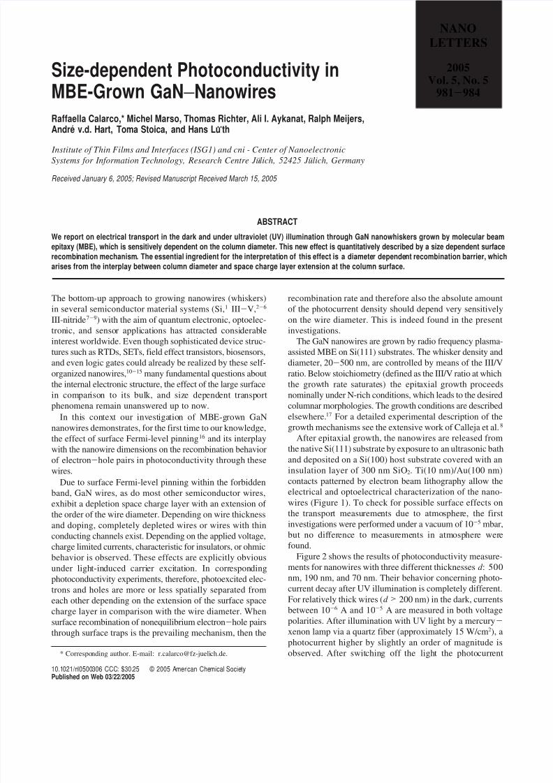
electrical and optoelectrical characterization of the nano-
wires (Figure 1). To check for possible surface effects on
the transport measurements due to atmosphere, the first
investigations were performed under a vacuum of 10-5 mbar,
but no difference to measurements in atmosphere were
found.Figure 2 shows the results of photoconductivity measure-
ments for nanowires with three different thicknesses d : 500
nm, 190 nm, and 70 nm. Their behavior concerning photo-
current decay after UV illumination is completely different.
For relatively thick wires (d > 200 nm) in the dark, currents
between 10-6 A and 10-5 A are measured in both voltage
polarities. After illumination with UV light by a mercury-
xenon lamp via a quartz fiber (approximately 15 W/cm2), a
photocurrent higher by slightly an order of magnitude is
observed. After switching off the light the photocurrent* Corresponding author. E-mail: [email protected].
NANO
LETTERS
2005Vol. 5, No. 5
981-984
10.1021/nl0500306 CCC: $30.25 © 2005 American Chemical SocietyPublished on Web 03/22/2005
8/3/2019 Bild der Frau, Oct 2011
http://slidepdf.com/reader/full/bild-der-frau-oct-2011 2/4
decays fast, but not to the dark current value; it rather stays
as a persistent photocurrent (in the dark), even 120 s after
the end of the illumination at approximately double the dark current value (Figure 2a). This effect of a persistent photo-
current is observed for wires with diameters down to about
100 nm. For the example in Figure 2b with d ) 190 nm the
photocurrent upon UV illumination decreases each time when
the light is switched off for some short period ∆t ) 1-2 s,
but does not reach the dark current value. A considerable
current persists in the dark periods. The effect is also clearly
seen from the time transient of the photocurrent in the 500
nm sample (Figure 3), where even after 5 min the current
exceeds the initial dark value by about 3 × 10⁻⁶A.
Thinner wires with diameters below about 100 nm (see
example in Figure 2b with d ) 70 nm), in contrast, exhibit
a fast photoresponse. For the 70 nm sample the maximum
observed photocurrents reach values at around 10-8 A.
Control experiments have shown that the measured dark
current of this sample is a parasitic background current not
related to transport through the GaN column. Photocurrents
in these thin GaN columns decay rapidly in the dark, which
demonstrates that there is no persistent photocurrent anymore.
Such a fast photoresponse was also observed by Han et al.18
on 15 nm thin GaN nanowires, but without an interpretationof the effect.
This general pattern of size dependent photocurrents is
also clearly seen when one plots the measured photocurrent
(as additive to dark current or parasitic background), at a
bias voltage of about 1 V; more precisely, an electric field
of 1 V/ µm, to account for different electrode spacings, versus
GaN nanowire diameter (Figure 4). While for wire diameters
above 100 nm the photocurrent changes only slightly with
diameter, below approximately 80 nm a sharp drop to
immeasurable values is observed.
Figure 1. SEM picture of a nanowire on Si host substrate, withTi/Au contact electrodes. Nanowire diameter: 70 nm.
Figure 2. Current-voltage characteristics of GaN nanowires withdifferent diameters with and without UV illumination. (a) 500 nmsample, dark and under steady-state UV illumination. (b) 190 nmand 70 nm samples, dark and under steady-state UV illumination,as well as under periodic UV illumination (dash-dotted). Thebehavior of the current after switching off the light (persistentphotoconductivity) depends on the diameter.
Figure 3. Current transient after 1 min of UV illumination (15W/cm2) of the 500 nm sample.
Figure 4. Photocurrent with UV illumination of approximately15 W/cm2 versus whisker diameter. The kink in the fitting curveat 85 nm indicates the critical diameter d crit, where the surfacedepletion layer just completely depletes the nanowire. For smallerdiameters the photocurrent shows an exponential decrease, for largerdiameters the photocurrent is proportional to the wire diameter.
982 Nano Lett., Vol. 5, No. 5, 2005
8/3/2019 Bild der Frau, Oct 2011
http://slidepdf.com/reader/full/bild-der-frau-oct-2011 3/4
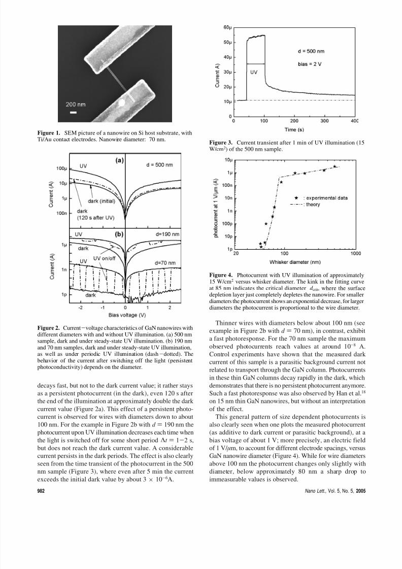
A double logarithmic plot of the current-voltage char-
acteristics (Figure 5) is helpful for a better understanding of
the phenomena. For the 190 nm sample, the photocurrent
under stationary illumination follows essentially a linear
dependence on bias voltage, as is expected for ohmic
behavior of a conducting channel in the whisker. Further-
more, this ohmic behavior, which is also found for the 500
nm thick sample in Figure 2a, both in the dark and with UV
illumination (at least up to 0.4 V), clearly demonstrates that
the contacts are largely ohmic and that effects due to
Schottky barriers at the contacts can be neglected. This is
expected from literature data for Ti/Au contacts.19 However,
the dark current, 3 orders of magnitude below the photo-current at bias voltages between 0.01 and 0.1 V, turns into
a V2 to V3 voltage dependence at bias voltages above 0.1
V. This behavior is characteristic for space charge limited
currents in insulators.20 A similar effect is also observed for
the 90 nm column. The photocurrent is essentially linear
(ohmic) in voltage, while the dark current is below the
measurement limit for voltages below 1 V and then shows
a space charge limited current behavior.
From the observation of space charge limited currents we
conclude that dark and photocurrents in these GaN columns
are governed by depletion space charge layers, which are
due to Fermi-level pinning at the surface of the nanocolumns.
From previous photoemission spectroscopy studies on GaNsurfaces, Fermi-level pinning is expected at about 0.5-0.6
eV below the conduction band edge.21 Assuming an n-type
background doping in the 1017cm-3 range, the depletion space
charge layers should have extensions of 50 to 100 nm into
the bulk. Depending on the column diameter the whiskers,
therefore, are completely depleted at small diameters (<80
nm) or have a tight open conducting channel at diameters
above 100 nm. But even under those conditions the columns
are essentially insulators in the dark due to their depletion
space charge layers. Dark currents, at least for diameters
below 200 nm, are space charge limited, as is characteristic
for insulators. Only the higher carrier densities under UV
light illumination allow ohmic behavior for diameters above
100 nm.
The existence of depletion space charge layers at the
column surface also explains the size dependent photocurrentbehavior (Figs. 2, 4) quantitatively.
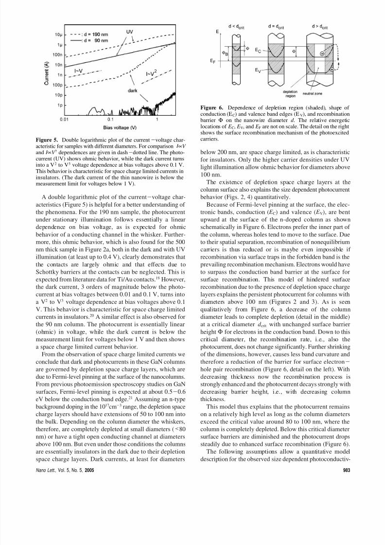
Because of Fermi-level pinning at the surface, the elec-
tronic bands, conduction ( E C) and valence ( E V), are bent
upward at the surface of the n-doped column as shown
schematically in Figure 6. Electrons prefer the inner part of
the column, whereas holes tend to move to the surface. Due
to their spatial separation, recombination of nonequilibrium
carriers is thus reduced or is maybe even impossible if
recombination via surface traps in the forbidden band is the
prevailing recombination mechanism. Electrons would have
to surpass the conduction band barrier at the surface for
surface recombination. This model of hindered surface
recombination due to the presence of depletion space chargelayers explains the persistent photocurrent for columns with
diameters above 100 nm (Figures 2 and 3). As is seen
qualitatively from Figure 6, a decrease of the column
diameter leads to complete depletion (detail in the middle)
at a critical diameter d crit with unchanged surface barrier
heightΦ for electrons in the conduction band. Down to this
critical diameter, the recombination rate, i.e., also the
photocurrent, does not change significantly. Further shrinking
of the dimensions, however, causes less band curvature and
therefore a reduction of the barrier for surface electron-
hole pair recombination (Figure 6, detail on the left). With
decreasing thickness now the recombination process is
strongly enhanced and the photocurrent decays strongly withdecreasing barrier height, i.e., with decreasing column
thickness.
This model thus explains that the photocurrent remains
on a relatively high level as long as the column diameters
exceed the critical value around 80 to 100 nm, where the
column is completely depleted. Below this critical diameter
surface barriers are diminished and the photocurrent drops
steadily due to enhanced surface recombination (Figure 6).
The following assumptions allow a quantitative model
description for the observed size dependent photoconductiv-
Figure 5. Double logarithmic plot of the current-voltage char-acteristic for samples with different diameters. For comparison I ∝V and I ∝V 2 dependences are given in dash-dotted line. The photo-current (UV) shows ohmic behavior, while the dark current turnsinto a V2 to V3 voltage dependence at bias voltages above 0.1 V.This behavior is characteristic for space charge limited currents ininsulators. (The dark current of the thin nanowire is below themeasurement limit for voltages below 1 V).
Figure 6. Dependence of depletion region (shaded), shape of conduction (EC) and valence band edges (EV), and recombinationbarrier Φ on the nanowire diameter d . The relative energeticlocations of E C, E V, and E F are not on scale. The detail on the rightshows the surface recombination mechanism of the photoexcitedcarriers.
Nano Lett., Vol. 5, No. 5, 2005 983
8/3/2019 Bild der Frau, Oct 2011
http://slidepdf.com/reader/full/bild-der-frau-oct-2011 4/4
ity. (i) The nanocolumns behave like a photoconductor
without Schottky-contacts at the metallization. (ii) The optical
absorption length for photons is much larger than the column
diameter, such that photoexcitation is homogeneous all over
the sample. (iii) Photogenerated carriers do not significantly
affect the potential, i.e., the band structure within the column.
(iv) The time decay of the persistent photocurrent is
essentially due to surface recombination, where holes are
pushed to the surface due to the surface band bending and
electrons have to overcome the corresponding surface barrier(Figure 6) in order to recombine. Under these conditions we
calculate the stationary photocurrent from the balance
between generation rate (proportional to absorption constant,
column volume, and irradiated light intensity) and surface
recombination rate (proportional to column surface and
recombination rate). The recombination rate is essentially
given by an exponential term exp(-φ / kT ), where the barrier
for electrons to recombine with holes amounts to
For d > d crit (minimum diameter for a fully depleted column)
a constant barrier height (eq 1b) with N D as donor concentra-
tion and 0 as dielectric constant of GaN causes a nearly
constant (slightly varying) photocurrent (proportional to
column diameter), as is observed in the experiment (Figure
4). For column diameters d < d crit, the recombination barrier
φ depends quadratically on the column diameter d (eq 1a)
and gives rise to a sharp exponential drop of the photocurrent.
The described theoretical model yields a nearly perfect
fit to the measured data (Figure 4). Three fitting parameters
are obtained numerically. One parameter, essentially the
proportionality factor between the photocurrent and the
exponential decay term, contains details about the electron-
hole pair generation mechanism, which are not well-known
so far. The second fitting parameter, the donor concentration
N D, is obtained as N D ) 6.25 × 1017cm-3. This N D value
corresponds well with doping levels obtained under standard
MBE conditions for GaN layers. It is worth emphasizing
that the unintentional doping in nanocolumns is obviously
not different from that during layer growth. Because of
different growth conditions for columns (N-rich) and layers
(Ga-rich), one would expect different dopant incorporation.
The third fitting parameter, the barrier height φB at diameters
above d crit (eq 1b), follows as 0.55 eV. This barrier valuecorresponds very well to the surface potential ( E C - E F) (see
Figure 6), which has been determined to be between 0.5 and
0.6 eV 21 from photoemission spectroscopy (XPS) on clean
GaN layers. More details about the experiments and the
theoretical analysis will be given in a subsequent, more
extended paper.
In conclusion, our model of surface electron-hole pair
recombination excellently describes the unusual behavior of
size dependent persistent photocurrents in GaN nanocolumns.
The physical bases of the effect are size dependent recom-
bination barriers within the whiskers, which are due to the
interplay between column diameter and space charge exten-
sion.The described effects are of general importance for all
kinds of semiconductor nanowires, electronic transport
through these structures, and in particular applications of
nanowires in optoelectronics and sensor technology.
References
(1) Lauhon, L.; Gudiksen, M.; Wang, D.; Lieber, C. Nature 2002, 420,57.
(2) Gudiksen, M.; Lauhon, L.; Wang, J.; Smith, D.; Lieber, C. Nature2002, 415, 617.
(3) Wang, J.; Gudiksen, M.; Duan, X.; Cui, Y.; Lieber, C. Science 2001,293, 1455.
(4) Hiruma, K.; Yazawa, M.; Haraguchi, K.; Ogawa, K.; Katsuyama,T.; Koguchi, M.; Kakibayashi, H. J. Appl. Phys. 1993, 74, 3162.
(5) Ohlsson, B.; Bjork, M.; Magnusson, M.; Deppert, K.; Samuelson,L.; Wallenberg, L. Appl. Phys. Lett. 2001, 79, 3335.
(6) Ohlsson, B.; Bjork, M.; Persson, A.; Thelander, C.; Wallenberg, L.;Magnusson, M.; Deppert, K.; Samuelson, L. Physica E 2002, 13,1126.
(7) Sanchez-Paramo, J.; Calleja, J.; Sanchez-Garcia, M.; Calleja, E.; Jahn,U. Physica E 2002, 13, 1070.
(8) Calleja, E.; Sanchez-Garcia, M.; Sanchez, F.; Calle, F.; Naranjo, F.;Munoz, E.; Jahn, U.; Ploog, K. Phys. ReV. B 2000, 62, 16826.
(9) Ristic, J.; Calleja, E.; Sanchez-Garcia, M.; Ulloa, J.; Sanchez-Paramo,J.; Calleja, J.; Jahn, U.; Trampert, A.; Ploog, K. Phys. ReV. B 2003,68, 125305.
(10) Thelander, C.; Mårtensson, T.; Bjork, M.; Ohlsson, B.; Larsson, M.;Wallenberg, L.; Samuelson, L. Appl. Phys. Lett. 2003, 83, 2052.
(11) Greytak, A.; Lauhon, L.; Gudiksen, M.; Lieber, C. Appl. Phys. Lett.2004, 84, 4176.
(12) Duan, X.; Huang, Y.; Agarwal, R.; Lieber, C. Nature 2003, 421,
241.(13) Zhong, Z.; Wang, D.; Cui, Y.; Bockrath, M.; Lieber, C. Science 2003,
302, 1377.(14) Bjork, M.; Ohlsson, B.; Thelander, C.; Persson, A.; Deppert, K.;
Wallenberg, L.; Samuelson, L. Appl. Phys. Lett. 2002, 81, 4458.(15) Bjork, M.; Ohlsson, B.; Sass, T.; Persson, A.; Thelander, C.;
Magnusson, M.; Deppert, K.; Wallenberg, L.; Samuelson, L. Appl.Phys. Lett. 2002, 80, 1058.
(16) Luth, H. Solid Surfaces, Interfaces and Thin Films, 4th ed.;Springer: Berlin, Heidelberg, 2001; Chapter 7.
(17) Calarco, R.; Marso, M.; Meijers, R.; Richter, T.; Aykanat, A. I.;Stoica, T.; Luth, H. Proceedings of the ASDAM ‘04 Conference,Smolenice, Slovakia, 2004, 9.
(18) Han, S.; Jin, W.; Zhang, D.; Tang, T.; Li, C.; Liu, X.; Liu, Z.; Lei,B.; Zhou, C. Chem. Phys. Lett. 2004, 389, 176.
(19) Schmitz, A. C.; Ping, A. T.; Khan, M. A.; Chen, Q.; Yang, J. W.;Adesida, I. Semicond. Sci. Technol. 1996, 11, 1464.
(20) Rose, A. Phys. ReV. 1955, 97 , 1538.(21) Kocan, M.; Rizzi, A.; Luth, H.; Keller, S.; Mishra, U. K. Phys. Status
Solidi B 2002, 234, 773.
NL0500306
φ ) eN Dd 2 /160 for d < d crit (1a)
φ ) eN D
d 2
crit /16
0for d > d
crit(1b)
984 Nano Lett., Vol. 5, No. 5, 2005


![Optische Koh arenztomogra e (OCT) - TU Dresden€¦ · Die OCT bietet zudem M oglichkeiten der Dopplerbildgebung zur Blut ussmessung [9] und der polarisationssensitiven Darstellung](https://img.pdfslide.org/doc/110x75/605aea8f5389c22ae731e5a3/optische-koh-arenztomogra-e-oct-tu-dresden-die-oct-bietet-zudem-m-oglichkeiten.jpg)


![arXiv:2004.03586v2 [eess.AS] 5 Oct 2020](https://img.pdfslide.org/doc/110x75/61906c931657e5535c18d40f/arxiv200403586v2-eessas-5-oct-2020.jpg)