Embed Size (px)
Citation preview
Segregation of Antimony in InP in MOVPE
vorgelegt vonDiplom-Physiker
Stefan Weeke aus Krefeld
Von der Fakultät II - Mathematik und Naturwissenschaftender Technischen Universität Berlin
zur Erlangung des akademischen Grades Doktor der Naturwissenschaften
Dr.rer.nat.
genehmigte Dissertation
Promotionsausschuss:
Vorsitzender: Prof. Dr. Michael Lehmann
Berichter/Gutachter: Prof. Dr. Wolfgang Richter
Berichter/Gutachter: Prof. Dr. Michael Kneissl
Tag der wissenschaftlichen Aussprache: 30.05.2008
D 83
Berlin 2008

II
III
Stefan Weeke – Segregation of antimony in InP in MOVPE
Abstract
In dieser Arbeit wurde die Segregation von Antimon in Indium Phosphid in der MetalOrganischen Gasphasen Epitaxy (MOVPE) systematisch untersucht. Dazu wurde zunächst inder MOVPE Tri-Methly-Antimon (TMSb) auf Phosphin stabilisierte InP Oberflächenaufgelassen. Dabei stellt sich eine antimonreiche Sb/InP Oberfläche ein, die ein für dieAntimonide typisches Spektrum in der Reflexions Anisotropie Spektroskopie (RAS) zeigt.Es werden sowohl die Adsorption und Desorption von Antimon auf InP untersucht, als auchder Einbau von Sb beim Überwachsen der Sb/InP Oberfläche mit InP. Dazu werden dieWachstumsparameter Temperatur, TMSb-Partialdruck und –Auflasszeit systematisch variiertund auf ihren Einfluß hin untersucht. Die Experimente werden in-situ mit RAS beobachtet,und die gewonnenen Daten mit ex-situ Untersuchungen wie Röntgendiffraktometrie (XRD)und Sekundär-Ionen Massenspektroskopie (SIMS) korreliert.Es wird gezeigt, das sich durch Auflassen von TMSb binnen weniger Sekunden eine stabileSb/InP Oberfläche bildet, die sich unter weiterer Zugabe von TMSb nicht mehr verändert.Dieser Prozess wird vom Partialdruck nur wenig beeinflusst. Die Desorption von Sb verläuftdagegen sehr langsam, und es werden zwei wesentliche Prozesse unterschieden: DieDesorption von überschüssigem Sb von der Oberfläche und die Formierung der MOVPEpräparierten InP (2x1) Oberfläche. Die Geschwindigkeit von Adsorption und Desorptionnimmt mit der Temperatur zu. Eine Erhöhung des TMSb Partialdrucks hat ab einemkritischen Wert keinen Einfluß auf die Desorptionszeit.Beim Überwachsen der Sb/InP Oberfläche mit InP wird der entgegengesetzteTemperaturverlauf beobachtet: Mit zunehmender Wachstumstemperatur wird dasantimontypische RAS-Spektrum länger beobachtet. Eine Analyse der gewachsenen Schichtenmit XRD und SIMS zeigt die Formation eines InPSb Doppel-Quantenwells. Eine Schichtfindet sich an der Grenzfläche, die zweite 50 – 120 nm tief im InP. Die Lage der zweitenInPSb Schicht kann mit dem verschwinden der Sb Signatur in der RAS korreliert werden. DieDistanz zwischen erster und zweiter InPSb steigt mit zunehmender Wachstumstemperatur an,bis sie bei 580°C durch zunehmende Desorption stagniert. SIMS Messungen zeigen, daß derSb Gehalt der InPSb Schicht an der Grenzfläche temperaturunhabhängig ist, während derGehalt der zweiten Schicht linear mit steigender Temperatur abnimmt. Der Sb-Gehalt in derzweiten Schicht hängt alleine von der Temperatur ab, nicht aber vom verwendeten SbPartialdruck.Die systematische Untersuchung von verspannten InPSb/InP Diffusions Übergittern zeigt, dasnur ein geringer Teil der ursprüglich auf der Oberfläche deponierten Antimons in den InPSbSchichten eingebaut wird. Der Großteil des Antimons segregiert in die InP Barrieren.Mittels eines linearen Segregationsmodels wird gezeigt, das der Segregationskoeffizient vonSb beinahe 1 ist.Die Formation des Doppelquantenwells wird mit einem Modell des spannungsindiziertenOberflächenschmelzens erklärt. Beim Auflassen von Antimon bildet sich eine Sb – reichequasi flüssige Oberflächenschmelze. Durch Sb ↔ P Austausch und Desorption wird der SbGehalt der Schicht so lange reduziert, bis sie erstarrt.

IV
Teile dieser Arbeit wurden bereits veröffentlicht in:
1. Segregation and desorption of antimony in InP (001) in MOVPEJournal of Crystal Growth Volume: 298, Complete, January, 2007, pp. 159-162Weeke, S.; Leyer, M.; Pristovsek, M.; Brunner, F.; Weyers, M.; Richter, W.
2. Growth monitoring of GaAsSb:C/InP heterostructures with reflectance anisotropyspectroscopyJournal of Crystal Growth Volume: 272, Issue: 1-4, December 10, 2004, pp. 111-117Brunner, F.; Weeke, S.; Zorn, M.; Weyers, M.
V
Content
1. Introduction........................................................................................................................... 12. Growth of antimonides inMOCVD..................................................................................... 32.1 Growth of antimonides........................................................................................................... 3
2.2 Applications........................................................................................................................... 4
2.3 The 6.1 Å family of semiconductor devices........................................................................... 6
3. Sample preparation and characterisation.......................................................................... 93.1 The MOVPE equipment......................................................................................................... 9
3.2 The MOVPE process............................................................................................................. 10
3.3 Reflectance Anisotropy Spectroscopy (RAS)....................................................................... 11
3.4 High Resolution X-ray Diffraction (HRXRD)...................................................................... 13
3.5 Secondary Ion Mass spectroscopy (SIMS)............................................................................ 15
4. Antimony on Indiumphosphide.......................................................................................... 174.1 InP surface reconstructions in MOCVD................................................................................ 18
4.2 III-Sb surface reconstructions................................................................................................ 20
4.3 Antimony on InP in MOCVD and MBE............................................................................... 22
4.4 Strain induced surface melting.............................................................................................. 24
4.4.1 Thermodynamic model......................................................................................................... 24
5. Experimental........................................................................................................................ 295.1 Monitoring Antimony in MOCVD........................................................................................ 29
6. Adsorption and desorption of Sb from InP surfaces in MOCVD................................... 336.1 Surface during Adsorption and Desorption of Sb on InP...................................................... 33
6.2 Langmuir model of adsorption and desorption..................................................................... 37
6.3 Adsorption and desorption of Sb on InP................................................................................ 41
7. Overgrowth of Sb-terminated InP surfaces.................................................................... .. 497.1 Thin InP layers...................................................................................................................... 49
7.2 InP layers thicker than 50 nm................................................................................................ 52
7.3 In-situ analysis....................................................................................................................... 55
7.4 Variation of exposure time and partial pressure................................................................ 56
7.5 Temperature dependence of double QW separation............................................................. 61
7.6 Stoichiometry of InPSb Quantum Wells............................................................................. . 65
7.6.1 Influence of the temperature................................................................................................. 65
7.6.2 Variation of Partial pressure................................................................................................ . 66

VI
8. Segregation of Sb in InPSb/InP superlattices.................................................................. 698.1 Models for segregation......................................................................................................... 69
8.2 XRD of indiffused InPSb/InP – Superlattices....................................................................... 72
9. Growth model....................................................................................................................... 819.1 The model of Sb surface melting........................................................................................... 81
10. Summary ........................................................................................................................ 8711. Bibliography........................................................................................................................ 89
1
1 Introduction
During the past decades III-V compound semiconductors and their alloys havedeveloped to be the key materials for high-speed electronic and optoelectronic devices,such as heterojunction bipolar transistors, lasers and photodetectors. Antimony basedmaterials have gained interest recently due to their favourable application in high-frequency devices used for high speed electronics and fiberoptic communication. Theseoptoelectronic devices consist of alternating thin films latticematched to InGaAs,InGaAsP, and InP. The interface structure between the alloy layers and indiumphosphide have a direct impact on the device performance. In particular, the interfaciallayers may contain defects and exhibit composition gradients that reduce electronmobility, enhance nonradiative carrier recombination, or alter quantum confinementenergies. Thus, in order to fabricate high-performance devices, one must be able controlthe interface structure on the atomic scale.
In recent years the material system of the antimonides has gained the attention ofresearchers. This is owed to their potential to replace InGaAs as base layer of InP basedDHBTs, driven by the demand to achieve terrahertz frequencies for communication,and the unique properties of the so called 6.1 Å family of semiconductors[1], whichconsists of InAs, GaSb and AlSb. These materials have the biggest lattice constantsamong the III-V semiconductors and offer with InAlSb the semiconductor with thesmallest bandgap. They offer exciting possibilities in bandgap engineering, usingstaggered and broken bandgap lineups, enabling Sb based detectors for the far and midinfrared. This region has so far been exclusively represented by mercury cadmiumtelluride and other II-VI compounds.
Besides the challenge of growing these materials, which will be reviewed in detail inchapter 2, the control of the interface is the most critical element for all theseapplications. Their performance depends on interface roughness, abruptness and layercomposition. The composition of an interfacial layer and he sharpness of a heterointerface strongly depends on the involved elements. Interfaces between Sb containinglayers and subsequent layers without Sb are known to suffer strongly from Sbsegregation. An interface that is of particular interest is the Sb-InP interface, motivatedby the interest in InP/GaAsSb HBt’s [2].
Metalorganic vapour-phase epitaxy (MOVPE) is nowadays widely used to fabricateIII-V semiconductor devices. During the growth of heterostructures, e.g., GaAsSb onInP, all group III and group V sources have to be switched simultaneously, e.g. thegroup III source must be changed from In to Ga and the group-V source must beswitched from phosphorus to arsenic and antimony. However, the strong tendency ofSb to accumulate on the growing surface challenges it to produce atomically abruptinterfaces [3,4] Switching procedures with growth interruptions have been implementedin an attempt to solve this problem. This has led to many studies that focus on the effectof precursor switching procedures on material properties[5,67].
In this work it will be shown that Sb in InP shows a striking segregational behaviourwhich originates from the accumulation of Sb on the surface and the extremely lowsegregation coefficient. While even the smallest amount of Sb tends to segregate on the
2
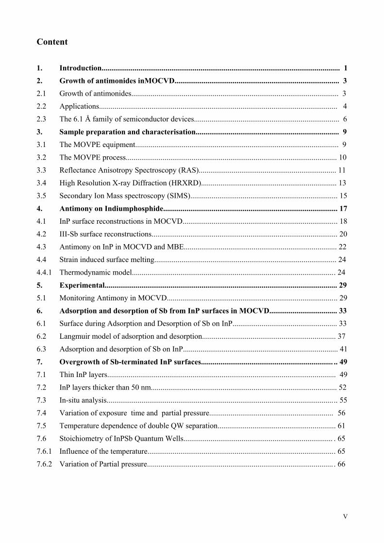
surface only very little is incorporated during growth. Additionally a very unusualphenomenon is observed: The self organised formation of an InPSb double quantumwell. The TEM picture below shows the InPSb QW formed at the interface at 550°C byindiffusion and the signature of a second QW 75 nm deep in the layer.
Figure 1: TEM image of the self organised InPSb double quantum well. At 540°Cthe DQW structure is visible.
3
2 Growth of antimonides in MOCVD
Metal Organic Vapour Phase Epitaxy (MOVPE) has be become the method of choicefor the growth of high quality III-Nitrides, -Phosphides and -Arsenides. MOVPE iscapable of growing atomically flat layers, sharp interfaces and control of layer thicknessin the range of few monolayers. MOVPE is considered to be advantageous to MBE forindustrial mass production for electronic and optoelectronic devices. MOVPE exhibitsadvantages compares to MBE, such as a higher growth rate of 1 to 5 µm/h, betterreproducibility of the growth process and easier wafer loading. Additionally MOVPEhas seen an upscaling to growth setups in the last 15 years from 1 x 2“ [6] up to 95 x 2“wafers [7].
Nevertheless, in recent years it has been demonstrated that several binary, ternary andquaternary antimonides can be as well grown in MOVPE. The growth of antimonideshas been reported first in MOCVD in 1969 by Manasevit and Simpson [8]. Theantimonides cover a wide range of band gap energies from 0,15 eV to 2.2 eV and can begrown on substrates such as GaAs, InP, InAs, GaSb and InSb. Thus they are potentiallyinteresting for a variety of electronic and optoelectronic applications. Those range fromemitters and detectors in the near and far infrared, high frequency transistors orphotovoltaic cells. The growth of antimonides differs strongly from the other III-Vmaterials, and faces several difficulties not known to other material systems. Those arethe low vapour pressure of Sb compared to other group V materials, the constraint to thekinetically controlled growth regime, the inexistence of a chemical stable hydride asprecursor, and last the lack of insulating Sb-substrates. The challenges and results of thegrowth of the binary and some of the ternary antimonides will be reviewed in thischapter. For more details some extensive reviews are available [9,10,11].
2.1 Growth of antimonides
For the growth of antimonides in MOVPE some special considerations have to be made.First of all the choice of a suitable precursor has to be considered. The main differencebetween the growth of antimonides and the other III-V semiconductors is that no stablehydride is available. Stibine (SbH3) is not storable and decomposes easily in the gasinlet system. Thus metalorganic precursors as trimethylantimony (TMSb),triethylantimony (TESb) or trisdimethylaminoantimony (TDMASb) are used. WhileTMSb and TESb are the only commercially available sources today. TDMASb has beensynthesised for the low temperature growth of InSb, alternative sources likeDiisopropylantimon-hydride (DIPSbH) or Tertiärbutyldimethylantimony (tBDMSb)lacked the requires purity. The low melting point of the antimonides and the lack of H-radicals from the hydride pyrolysis complicates the oxide removal during heating up.Due to the lower growth temperatures the Al-containing antimonides suffer from strongC and O background incorporation from the alkyl-sources. This special issue isreviewed in extend in reference [11]. While the Arsenides, Phosphides and nitrides aregrown with phosphine, arsine and ammonia at conditions of excess group V, the lowervapour pressure of the Sb requires that the V-III ratio has to be exactly adjusted.Furthermore most of the ternary and quaternary materials of interest are
4
thermodynamically unstable and show different forms of phase separation and ordering.To circumvent these difficulties growth is performed far away from equilibrium, whichrequires low temperatures between 350°C and 600°C.
The growth and processing of Sb based semiconductors differs significantly from thegrowth of the much better investigated Arsenides and Phosphides. The low meltingpoint of the antimonides limits the temperature range for growth. InSb for examplemelts at 527°C and must be grown below that temperature. The low equilibrium vapourpressure of Sb, which is in the range of the group III elements leads to accumulation ofSb on the surface. Thus the V/III ratio during growth is mostly held near unity. Lastthere is no stable hydride comparable to arsine or phosphine. The main obstacle ingrowing antimonides is the lack of suitable precursors for MOCVD. The hydride ofantimony, stibine, is not stable at any laboratory condition. Extensive research has beendone to produce suitable metal-organic precursors. Most of these material suffer fromhigh carbon incorporation and unwanted side reaction with the group III elements.Nowadays all publications are using Trimethyl-antimony or tri-ethyl-antimony.
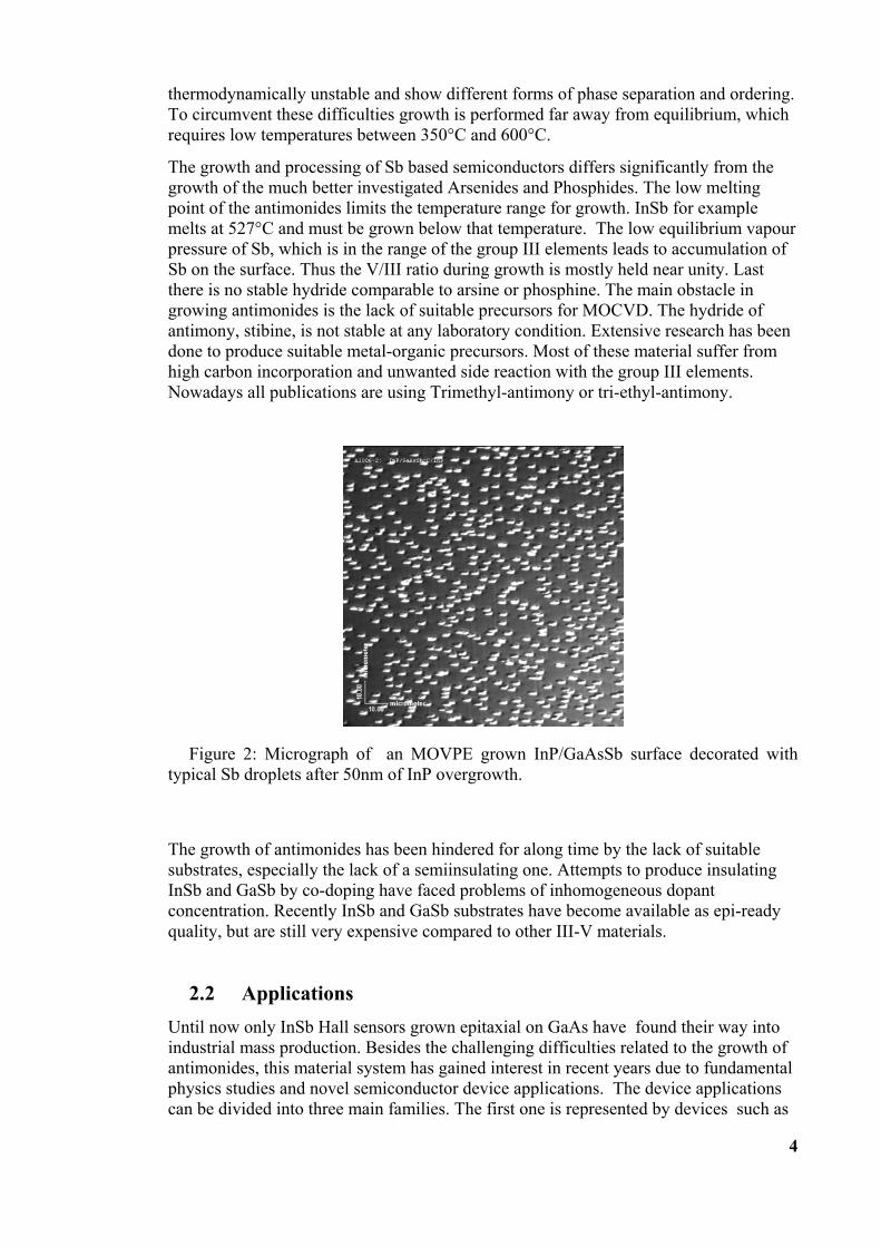
Figure 2: Micrograph of an MOVPE grown InP/GaAsSb surface decorated withtypical Sb droplets after 50nm of InP overgrowth.
The growth of antimonides has been hindered for along time by the lack of suitablesubstrates, especially the lack of a semiinsulating one. Attempts to produce insulatingInSb and GaSb by co-doping have faced problems of inhomogeneous dopantconcentration. Recently InSb and GaSb substrates have become available as epi-readyquality, but are still very expensive compared to other III-V materials.
2.2 ApplicationsUntil now only InSb Hall sensors grown epitaxial on GaAs have found their way intoindustrial mass production. Besides the challenging difficulties related to the growth ofantimonides, this material system has gained interest in recent years due to fundamentalphysics studies and novel semiconductor device applications. The device applicationscan be divided into three main families. The first one is represented by devices such as
5
Double Hetero Bipolar Transistors (DHBT) for high frequency applications, the secondone are triple junction solar cells or TPV’s (thermal photo voltaic). Those devices aregrown on InP and benefit from the narrow bandgap of ternary and quaternaryantimonides and the favourable type two band-alignment in Sb-InP heterojunctions. Thethird one are SL-structures for far and mid-infrared devices based on InAs. Realisationof these promising concepts for antimonides is much more difficult than other for otherIII-V materials. Structures based on Al-,GaSb/InAs are often referred to as the „6.1 Åfamily“ of semiconductor devices[1]
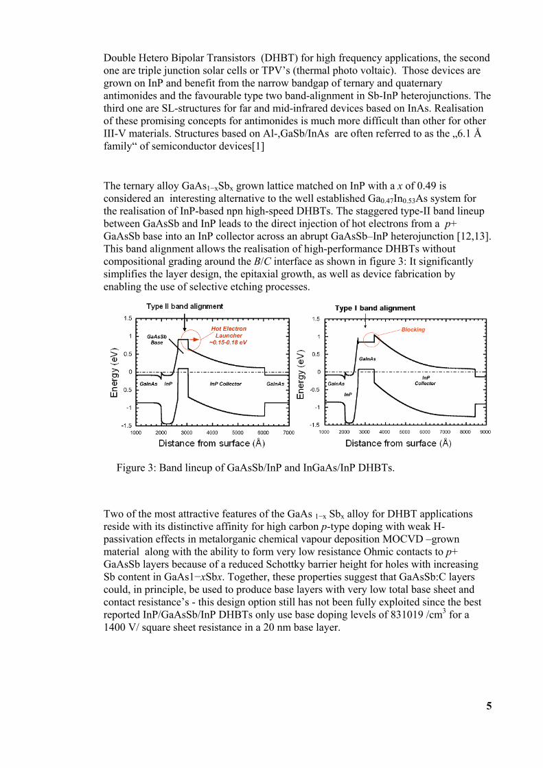
The ternary alloy GaAs1−xSbx grown lattice matched on InP with a x of 0.49 isconsidered an interesting alternative to the well established Ga0.47In0.53As system forthe realisation of InP-based npn high-speed DHBTs. The staggered type-II band lineupbetween GaAsSb and InP leads to the direct injection of hot electrons from a p+GaAsSb base into an InP collector across an abrupt GaAsSb–InP heterojunction [12,13].This band alignment allows the realisation of high-performance DHBTs withoutcompositional grading around the B/C interface as shown in figure 3: It significantlysimplifies the layer design, the epitaxial growth, as well as device fabrication byenabling the use of selective etching processes.
Figure 3: Band lineup of GaAsSb/InP and InGaAs/InP DHBTs.
Two of the most attractive features of the GaAs 1−x Sbx alloy for DHBT applicationsreside with its distinctive affinity for high carbon p-type doping with weak H-passivation effects in metalorganic chemical vapour deposition MOCVD –grownmaterial along with the ability to form very low resistance Ohmic contacts to p+GaAsSb layers because of a reduced Schottky barrier height for holes with increasingSb content in GaAs1−xSbx. Together, these properties suggest that GaAsSb:C layerscould, in principle, be used to produce base layers with very low total base sheet andcontact resistance’s - this design option still has not been fully exploited since the bestreported InP/GaAsSb/InP DHBTs only use base doping levels of 831019 /cm3 for a1400 V/ square sheet resistance in a 20 nm base layer.
6
2.3 The 6.1 Å family of semiconductor devices
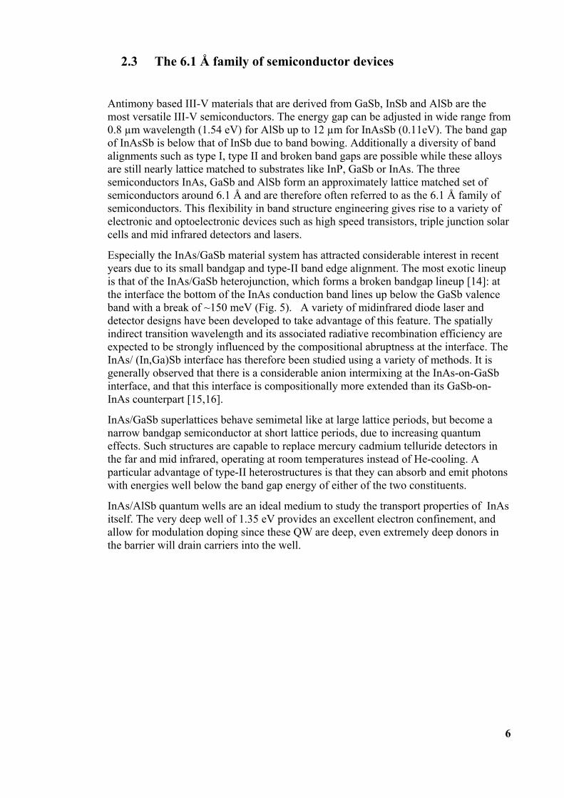
Antimony based III-V materials that are derived from GaSb, InSb and AlSb are themost versatile III-V semiconductors. The energy gap can be adjusted in wide range from0.8 µm wavelength (1.54 eV) for AlSb up to 12 µm for InAsSb (0.11eV). The band gapof InAsSb is below that of InSb due to band bowing. Additionally a diversity of bandalignments such as type I, type II and broken band gaps are possible while these alloysare still nearly lattice matched to substrates like InP, GaSb or InAs. The threesemiconductors InAs, GaSb and AlSb form an approximately lattice matched set ofsemiconductors around 6.1 Å and are therefore often referred to as the 6.1 Å family ofsemiconductors. This flexibility in band structure engineering gives rise to a variety ofelectronic and optoelectronic devices such as high speed transistors, triple junction solarcells and mid infrared detectors and lasers.
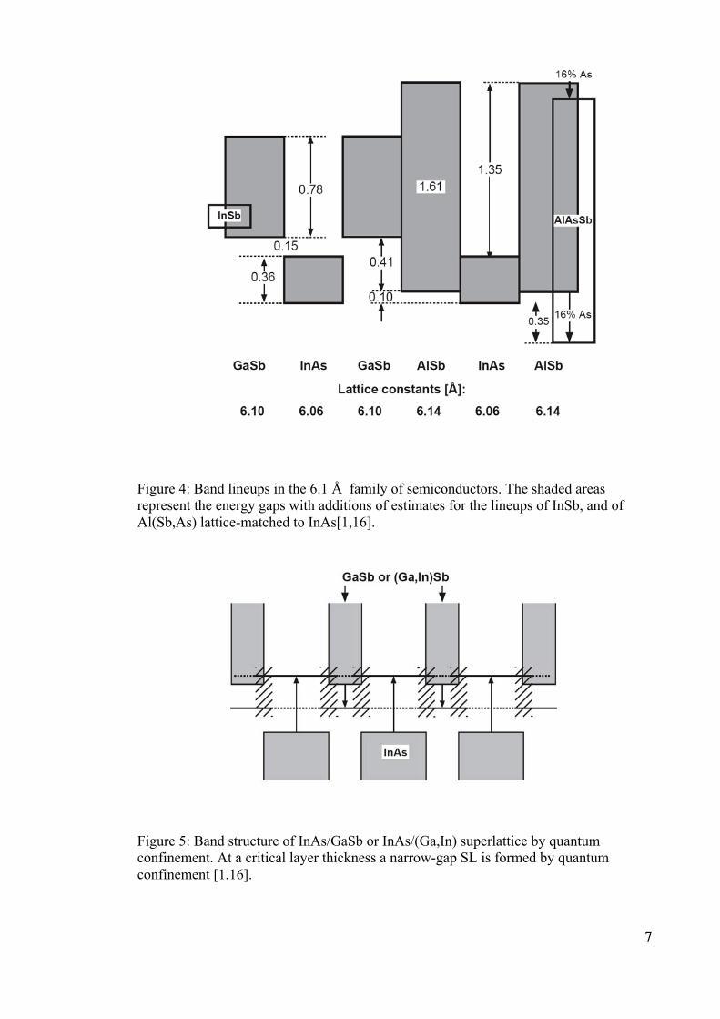
Especially the InAs/GaSb material system has attracted considerable interest in recentyears due to its small bandgap and type-II band edge alignment. The most exotic lineupis that of the InAs/GaSb heterojunction, which forms a broken bandgap lineup [14]: atthe interface the bottom of the InAs conduction band lines up below the GaSb valenceband with a break of ~150 meV (Fig. 5). A variety of midinfrared diode laser anddetector designs have been developed to take advantage of this feature. The spatiallyindirect transition wavelength and its associated radiative recombination efficiency areexpected to be strongly influenced by the compositional abruptness at the interface. TheInAs/ (In,Ga)Sb interface has therefore been studied using a variety of methods. It isgenerally observed that there is a considerable anion intermixing at the InAs-on-GaSbinterface, and that this interface is compositionally more extended than its GaSb-on-InAs counterpart [15,16].
InAs/GaSb superlattices behave semimetal like at large lattice periods, but become anarrow bandgap semiconductor at short lattice periods, due to increasing quantumeffects. Such structures are capable to replace mercury cadmium telluride detectors inthe far and mid infrared, operating at room temperatures instead of He-cooling. Aparticular advantage of type-II heterostructures is that they can absorb and emit photonswith energies well below the band gap energy of either of the two constituents.
InAs/AlSb quantum wells are an ideal medium to study the transport properties of InAsitself. The very deep well of 1.35 eV provides an excellent electron confinement, andallow for modulation doping since these QW are deep, even extremely deep donors inthe barrier will drain carriers into the well.
7
Figure 4: Band lineups in the 6.1 Å family of semiconductors. The shaded areasrepresent the energy gaps with additions of estimates for the lineups of InSb, and ofAl(Sb,As) lattice-matched to InAs[1,16].
Figure 5: Band structure of InAs/GaSb or InAs/(Ga,In) superlattice by quantumconfinement. At a critical layer thickness a narrow-gap SL is formed by quantumconfinement [1,16].
8
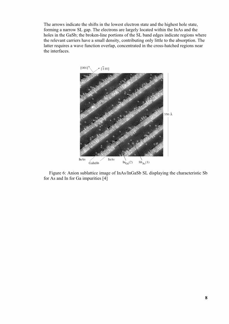
The arrows indicate the shifts in the lowest electron state and the highest hole state,forming a narrow SL gap. The electrons are largely located within the InAs and theholes in the GaSb; the broken-line portions of the SL band edges indicate regions wherethe relevant carriers have a small density, contributing only little to the absorption. Thelatter requires a wave function overlap, concentrated in the cross-hatched regions nearthe interfaces.
Figure 6: Anion sublattice image of InAs/InGaSb SL displaying the characteristic Sbfor As and In for Ga impurities [4]
9
3 Sample preparation and characterisation
The samples presented in this work were prepared by Metal Organic Vapour PhaseEpitaxy – in short MOVPE , which is nowadays the standard method for the industrialgrowth of compound semiconductor heterostructures. This method has been developedin the early 60s [8,17,18]. The principal aspects can be found in several books coveringMOVPE growth [19,20,21]. Therefore only the specialities of the equipment used willbe described.
The sample characterisation has been focused on in-situ monitoring with Reflectance-Anisotropy-Spectroscopy (RAS) and ex-situ characterisation with Secondary Ion MassSpectroscopy (SIMS) and X-Ray Diffraction (XRD). The following description willfocus on some details usually not found in textbooks or review articles.
3.1 The MOVPE equipment
The MOVPE equipment used in this work is the ancestor of the small type horizontalreactors that were introduced by Aixtron for research and has been modified for in-situmonitoring of the growth process. It consists of a horizontal quartz glass reactorenclosing the liner tube. The susceptor is SiC coated graphite. Heating is performed by3 x 1000 Watt halogen lamps, with a strong infrared emission characteristic, which arelocated below the reactor. The temperature is measured by a thermocouple inside thesusceptor, temperature calibration was done with an AlSi euthecticum at 576°C. As aspeciality the reactor has been modified with three purged strain free optical windows,allowing simultaneously SE (spectroscopic ellipsometry) and RAS (Reflectanceanisotropy spectroscopy) measurements.
Typical growth conditions are 100 mbar at a total gas flow of 3000 ml. The carrier gasis purified H2 or alternatively N2 and accounts for 95 % of the total gas flow. Thisguaranties an quick exchange of the gas phase above the sample. The precursorsavailable for this work were phosphine (PH3), arsine (AsH3),Trimethylantimony(TMSb), tertiarybutylarsine (tbAs), Trimethylindium (TMIn) and triethylgallium(TEGa) In order to avoid prereactions of the precursors, they were supplied in separatelines to the gas inlet of the reactor to avoid prereactions.
A more detailed description of the MOVPE equipment can be found in references[22,23]
10
3.2 The MOVPE process
MOVPE of III/V semiconductors uses ether gaseous hydrides or liquid metal-organiccompounds as precursors. For the group V elements the respective hydrides such asArsine (AsH3) or Phosphine (PH3) are commonly used. For the antimonides, where nostable hydride is available, also group V is a metal-organic compounds like TMSb (tri-methyl antimony).
Due to the higher vapour pressure of the group V element of the classical III-Vsemiconductors, the gas phase is usually supersaturated with the group V precursor tostabilise the surface, while the amount of group III precursor determines the growthrate. V/III ratios from 100 for the Arsenides up to several thousand for the nitrides arecommon. An exception is formed by the antimonides; due to the low vapour pressure ofSb V/III ratios close to unity are necessary.
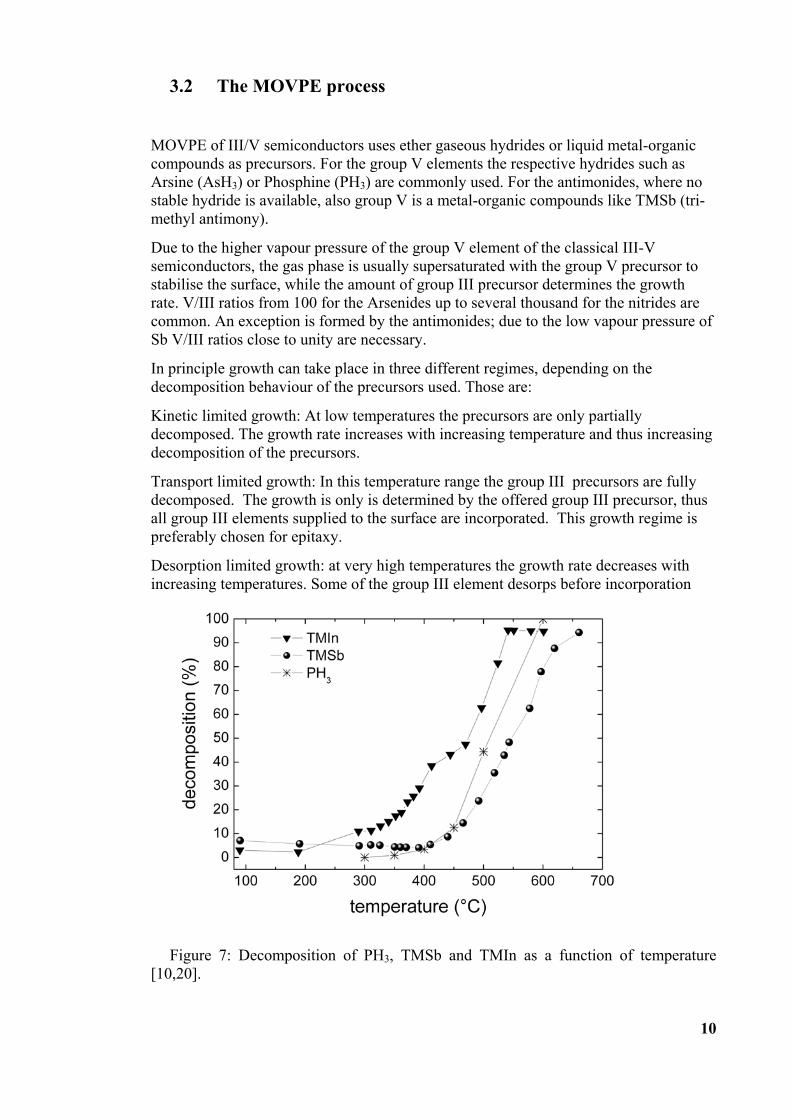
In principle growth can take place in three different regimes, depending on thedecomposition behaviour of the precursors used. Those are:
Kinetic limited growth: At low temperatures the precursors are only partiallydecomposed. The growth rate increases with increasing temperature and thus increasingdecomposition of the precursors.
Transport limited growth: In this temperature range the group III precursors are fullydecomposed. The growth is only is determined by the offered group III precursor, thusall group III elements supplied to the surface are incorporated. This growth regime ispreferably chosen for epitaxy.
Desorption limited growth: at very high temperatures the growth rate decreases withincreasing temperatures. Some of the group III element desorps before incorporation
Figure 7: Decomposition of PH3, TMSb and TMIn as a function of temperature[10,20].
11
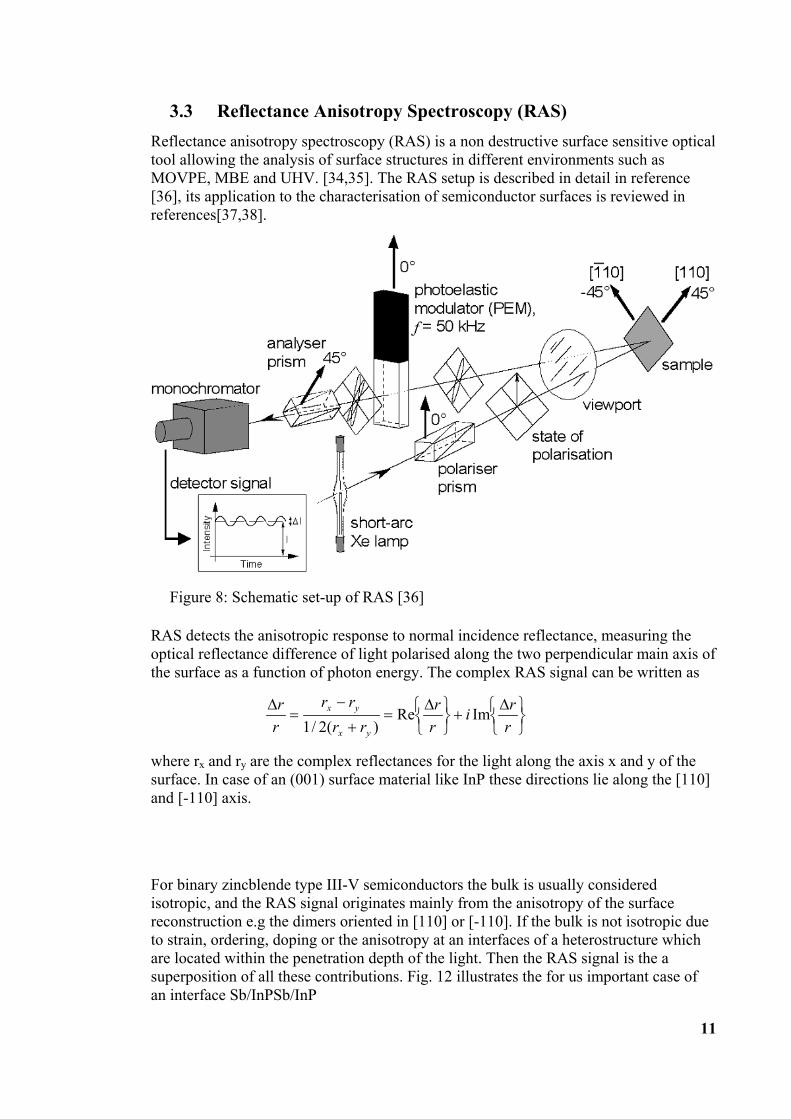
3.3 Reflectance Anisotropy Spectroscopy (RAS)Reflectance anisotropy spectroscopy (RAS) is a non destructive surface sensitive opticaltool allowing the analysis of surface structures in different environments such asMOVPE, MBE and UHV. [34,35]. The RAS setup is described in detail in reference[36], its application to the characterisation of semiconductor surfaces is reviewed inreferences[37,38].
Figure 8: Schematic set-up of RAS [36]
RAS detects the anisotropic response to normal incidence reflectance, measuring theoptical reflectance difference of light polarised along the two perpendicular main axis ofthe surface as a function of photon energy. The complex RAS signal can be written as
∆
+
∆
=+
−=
∆rri
rr
rrrr
rr
yx
yx ImRe)(2/1
where rx and ry are the complex reflectances for the light along the axis x and y of thesurface. In case of an (001) surface material like InP these directions lie along the [110]and [-110] axis.
For binary zincblende type III-V semiconductors the bulk is usually consideredisotropic, and the RAS signal originates mainly from the anisotropy of the surfacereconstruction e.g the dimers oriented in [110] or [-110]. If the bulk is not isotropic dueto strain, ordering, doping or the anisotropy at an interfaces of a heterostructure whichare located within the penetration depth of the light. Then the RAS signal is the asuperposition of all these contributions. Fig. 12 illustrates the for us important case ofan interface Sb/InPSb/InP
12
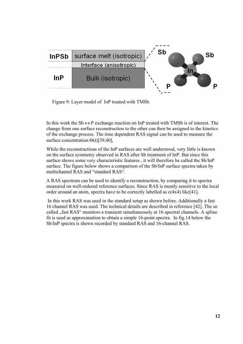
Figure 9: Layer model of InP treated with TMSb.
In this work the Sb ↔ P exchange reaction on InP treated with TMSb is of interest. Thechange from one surface reconstruction to the other can then be assigned to the kineticsof the exchange process. The time dependent RAS signal can be used to measure thesurface concentration Θ(t)[39,40].
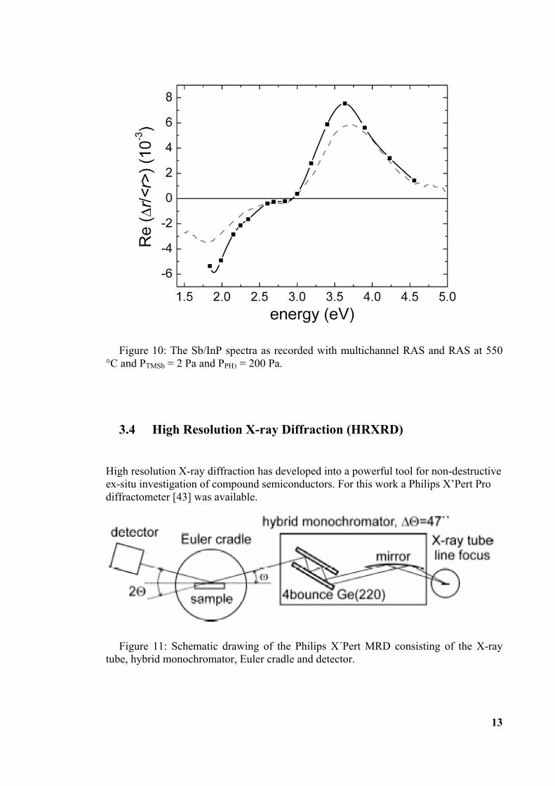
While the reconstructions of the InP surfaces are well understood, very little is knownon the surface symmetry observed in RAS after Sb treatment of InP. But since thissurface shows some very characteristic features , it will therefore be called the Sb/InPsurface. The figure below shows a comparison of the Sb/InP surface spectra taken bymultichannel RAS and “standard RAS“.
A RAS spectrum can be used to identify a reconstruction, by comparing it to spectrameasured on well-ordered reference surfaces. Since RAS is mostly sensitive to the localorder around an atom, spectra have to be correctly labelled as c(4x4) like[41].
In this work RAS was used in the standard setup as shown before. Additionally a fast16 channel RAS was used. The technical details are described in reference [42]. The socalled „fast RAS“ monitors a transient simultaneously at 16 spectral channels. A splinefit is used as approximation to obtain a simple 16-point spectra. In fig.14 below theSb/InP spectra is shown recorded by standard RAS and 16-channel RAS.
13
Figure 10: The Sb/InP spectra as recorded with multichannel RAS and RAS at 550°C and PTMSb = 2 Pa and PPH3 = 200 Pa.
3.4 High Resolution X-ray Diffraction (HRXRD)
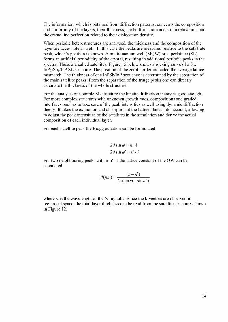
High resolution X-ray diffraction has developed into a powerful tool for non-destructiveex-situ investigation of compound semiconductors. For this work a Philips X’Pert Prodiffractometer [43] was available.
Figure 11: Schematic drawing of the Philips X´Pert MRD consisting of the X-raytube, hybrid monochromator, Euler cradle and detector.
14
The information, which is obtained from diffraction patterns, concerns the compositionand uniformity of the layers, their thickness, the built-in strain and strain relaxation, andthe crystalline perfection related to their dislocation density.
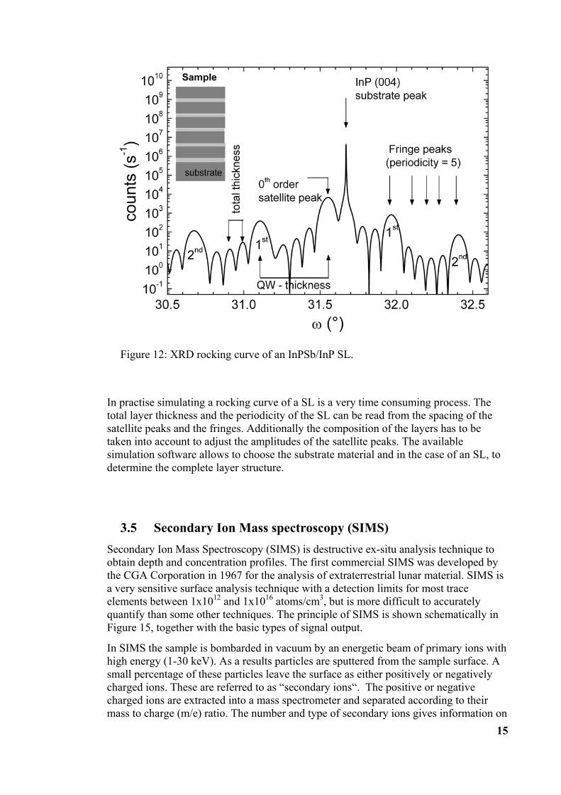
When periodic heterostructures are analysed, the thickness and the composition of thelayer are accessible as well. In this case the peaks are measured relative to the substratepeak, which’s position is known. A multiquantum well (MQW) or superlattice (SL)forms an artificial periodicity of the crystal, resulting in additional periodic peaks in thespectra. Those are called satellites. Figure 15 below shows a rocking curve of a 5 xInP95Sb5/InP SL structure. The position of the zeroth order indicated the average latticemismatch. The thickness of one InPSb/InP sequence is determined by the separation ofthe main satellite peaks. From the separation of the fringe peaks one can directlycalculate the thickness of the whole structure.
For the analysis of a simple SL structure the kinetic diffraction theory is good enough.For more complex structures with unknown growth rates, compositions and gradedinterfaces one has to take care of the peak intensities as well using dynamic diffractiontheory. It takes the extinction and absorption at the lattice planes into account, allowingto adjust the peak intensities of the satellites in the simulation and derive the actualcomposition of each individual layer.
For each satellite peak the Bragg equation can be formulated
λωλω⋅′=′
⋅=nd
ndsin2sin2
For two neighbouring peaks with n-n‘=1 the lattice constant of the QW can becalculated
)sin(sin2)()(
ωω ′−⋅′−
=nnnmd
where λ is the wavelength of the X-ray tube. Since the k-vectors are observed inreciprocal space, the total layer thickness can be read from the satellite structures shownin Figure 12.
15
Figure 12: XRD rocking curve of an InPSb/InP SL.
In practise simulating a rocking curve of a SL is a very time consuming process. Thetotal layer thickness and the periodicity of the SL can be read from the spacing of thesatellite peaks and the fringes. Additionally the composition of the layers has to betaken into account to adjust the amplitudes of the satellite peaks. The availablesimulation software allows to choose the substrate material and in the case of an SL, todetermine the complete layer structure.
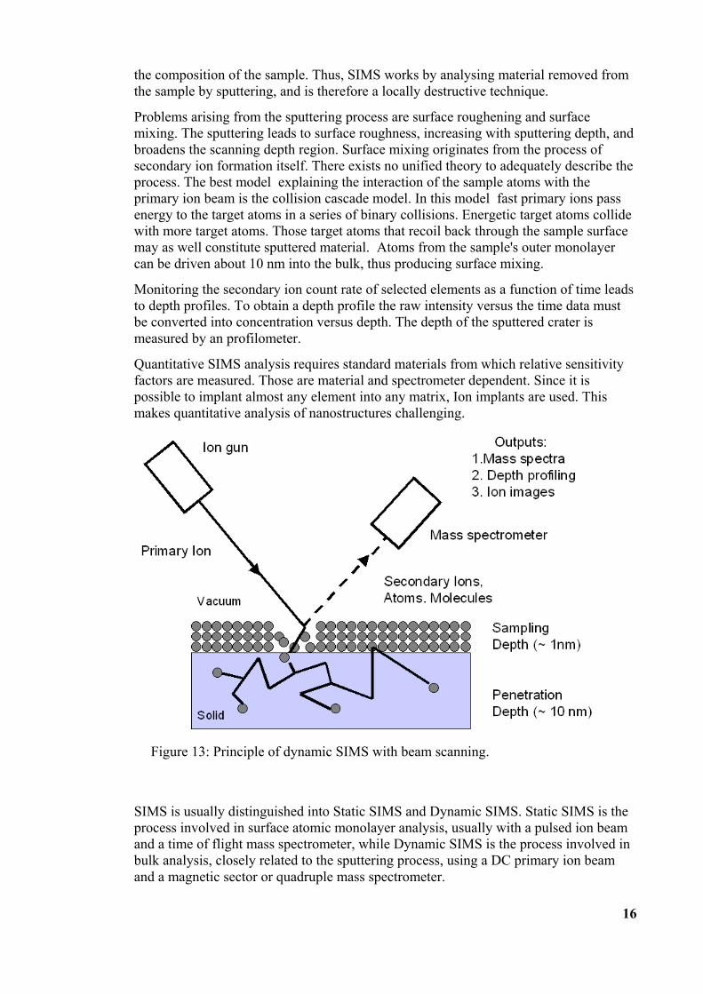
3.5 Secondary Ion Mass spectroscopy (SIMS)Secondary Ion Mass Spectroscopy (SIMS) is destructive ex-situ analysis technique toobtain depth and concentration profiles. The first commercial SIMS was developed bythe CGA Corporation in 1967 for the analysis of extraterrestrial lunar material. SIMS isa very sensitive surface analysis technique with a detection limits for most traceelements between 1x10¹² and 1x10¹⁶ atoms/cm3, but is more difficult to accuratelyquantify than some other techniques. The principle of SIMS is shown schematically inFigure 15, together with the basic types of signal output.
In SIMS the sample is bombarded in vacuum by an energetic beam of primary ions withhigh energy (1-30 keV). As a results particles are sputtered from the sample surface. Asmall percentage of these particles leave the surface as either positively or negativelycharged ions. These are referred to as “secondary ions“. The positive or negativecharged ions are extracted into a mass spectrometer and separated according to theirmass to charge (m/e) ratio. The number and type of secondary ions gives information on
16
the composition of the sample. Thus, SIMS works by analysing material removed fromthe sample by sputtering, and is therefore a locally destructive technique.
Problems arising from the sputtering process are surface roughening and surfacemixing. The sputtering leads to surface roughness, increasing with sputtering depth, andbroadens the scanning depth region. Surface mixing originates from the process ofsecondary ion formation itself. There exists no unified theory to adequately describe theprocess. The best model explaining the interaction of the sample atoms with theprimary ion beam is the collision cascade model. In this model fast primary ions passenergy to the target atoms in a series of binary collisions. Energetic target atoms collidewith more target atoms. Those target atoms that recoil back through the sample surfacemay as well constitute sputtered material. Atoms from the sample's outer monolayercan be driven about 10 nm into the bulk, thus producing surface mixing.
Monitoring the secondary ion count rate of selected elements as a function of time leadsto depth profiles. To obtain a depth profile the raw intensity versus the time data mustbe converted into concentration versus depth. The depth of the sputtered crater ismeasured by an profilometer.
Quantitative SIMS analysis requires standard materials from which relative sensitivityfactors are measured. Those are material and spectrometer dependent. Since it ispossible to implant almost any element into any matrix, Ion implants are used. Thismakes quantitative analysis of nanostructures challenging.
Figure 13: Principle of dynamic SIMS with beam scanning.
SIMS is usually distinguished into Static SIMS and Dynamic SIMS. Static SIMS is theprocess involved in surface atomic monolayer analysis, usually with a pulsed ion beamand a time of flight mass spectrometer, while Dynamic SIMS is the process involved inbulk analysis, closely related to the sputtering process, using a DC primary ion beamand a magnetic sector or quadruple mass spectrometer.
17
4 Antimony on Indiumphosphide
The reconstruction on the surface of a semiconductor plays a key role in understandinggrowth mechanisms occurring during MOCVD growth. It determines the kinetics ofadsorption, desorption and diffusion and provides a template for island nucleation.These are critical factors for the understanding of growth and the formation ofinterfaces. The quality of interfaces is of critical interest for modern quantum welldevices, since most of the heterostructure devices consist of ultrathin layers, so thateven the smallest variation in film thickness and interfacial roughness can affect thedevice performance. To achieve the level of control to grow such heterostructures adetailed understanding of the relevant surface reconstructions and the mechanisms bywhich epitaxy proceeds is beneficial.
The structures of III-P and III-As surface reconstruction under typical MOCVD growthconditions have been investigated in detail, and are in general well understood[44,45].On the other hand, very little is known about the structure of the III-Sb reconstructionsin MOCVD. It is widely accepted that the surfaces of the III-V semiconductorsreconstruct in such a way that the dangling bonds of the group III atom are unoccupiedand all those of the group V atom are doubly occupied, with the resulting surfacebandgap being the one of the bulk. This principle, often referred to as the electroncounting rule, is the guide for building surface reconstructions[46]. The ECM has beensuccessfully applied to the III-As and III-V surface reconstructions, but not to III-Sbreconstructions. The structural models of the surface reconstructions of the later are stilldebated and in some cases even thought to violate the ECM or to be semimetallic. Mostefforts to investigate these surfaces structures have been done in MBE and vacuum,were the surface is accessible by methods such as Scanning Tunnel Microscopy (STM),Reflective High Energy Electron Diffraction (RHEED) and Low Energy ElectronDiffraction (LEED). In MOVPE the relevant reconstructions present during growth aregroup V rich due to the growth conditions. But the relevant Sb-surface reconstructionsmostly are poorly understood. This is owed to the difficulty to prepare these materials inMOCVD and the reduced accessibility to surface sensitive methods.
The surface reconstructions which are important for this work are the MOVPEprepared InP (2x1) reconstruction and the Sb terminated InP surface which is observedafter treatment of InP with TMSb. Since the actual structure of the second one is notknown, it will be referred to as the Sb/InP surface. It displays a broad peak around 3.8 –4 eV which is characteristic for the antimony containing III-V (001) surfaces whenobserved with RAS.
18
4.1 InP surface reconstructions in MOCVD
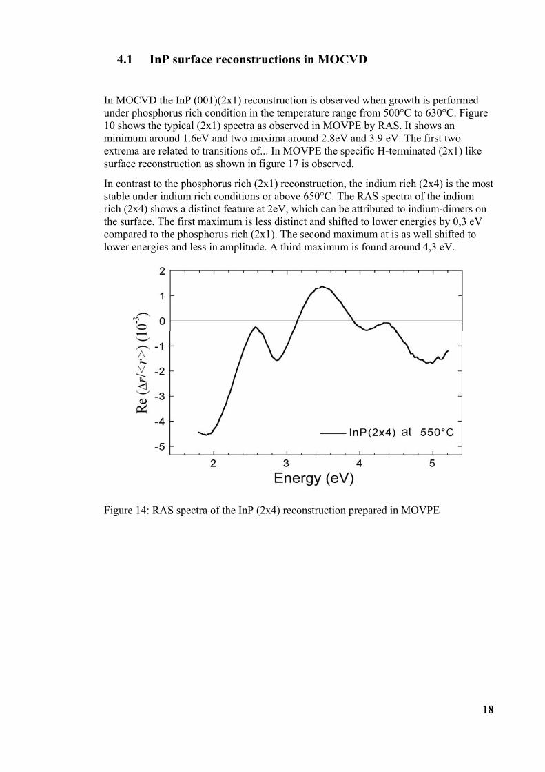
In MOCVD the InP (001)(2x1) reconstruction is observed when growth is performedunder phosphorus rich condition in the temperature range from 500°C to 630°C. Figure10 shows the typical (2x1) spectra as observed in MOVPE by RAS. It shows anminimum around 1.6eV and two maxima around 2.8eV and 3.9 eV. The first twoextrema are related to transitions of... In MOVPE the specific H-terminated (2x1) likesurface reconstruction as shown in figure 17 is observed.
In contrast to the phosphorus rich (2x1) reconstruction, the indium rich (2x4) is the moststable under indium rich conditions or above 650°C. The RAS spectra of the indiumrich (2x4) shows a distinct feature at 2eV, which can be attributed to indium-dimers onthe surface. The first maximum is less distinct and shifted to lower energies by 0,3 eVcompared to the phosphorus rich (2x1). The second maximum at is as well shifted tolower energies and less in amplitude. A third maximum is found around 4,3 eV.
Figure 14: RAS spectra of the InP (2x4) reconstruction prepared in MOVPE
19
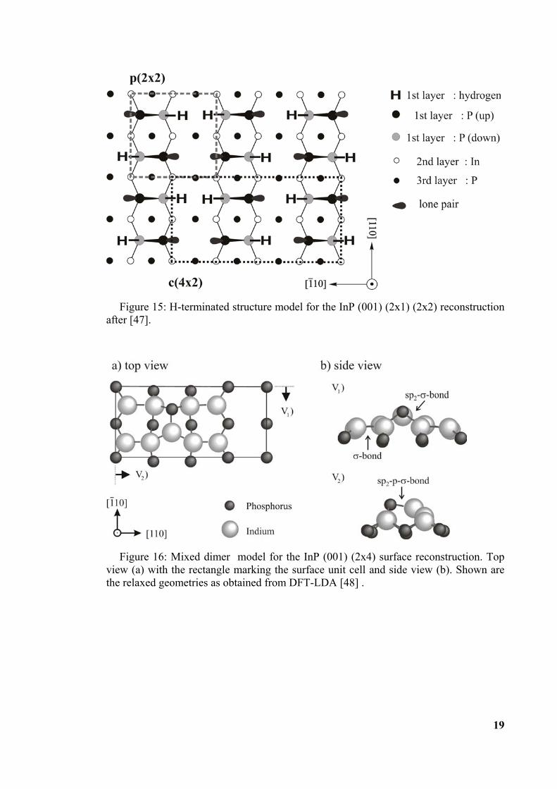
Figure 15: H-terminated structure model for the InP (001) (2x1) (2x2) reconstructionafter [47].
Figure 16: Mixed dimer model for the InP (001) (2x4) surface reconstruction. Topview (a) with the rectangle marking the surface unit cell and side view (b). Shown arethe relaxed geometries as obtained from DFT-LDA [48] .
20
4.2 III-Sb surface reconstructions
In contrast to the structure of III-P and III-As (001) surfaces under growth conditions,the structure of the III-Sb surfaces has been much less investigated, despite the growinginterest due to their potential for novel optoelectronic and electronic devices. Like onother III-V materials, several reconstructions have been observed on the binaryantimonides forming multiple Sb layers. Several of those reconstructions do not satisfythe electron counting rule so far, i.e. these surfaces have excess charges and areexpected to be either metallic or adsorbate stabilised [49].
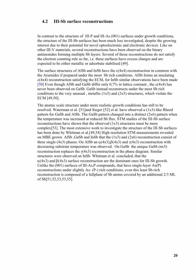
The surface structures of AlSb and InSb have the c(4x4) reconstruction in common withthe Arsenides if prepared under the most Sb rich conditions. AlSb forms an insulatingc(4x4) reconstruction satisfying the ECM, for InSb similar observations have been made[50] Even though AlSb and GaSb differ only 0,7% in lattice constant , the c(4x4) hasnever been observed on GaSb. GaSb instead reconstructs under the most Sb richconditions to the very unusual , metallic (1x5) and (2x5) structures, which violate theECM [49,50].
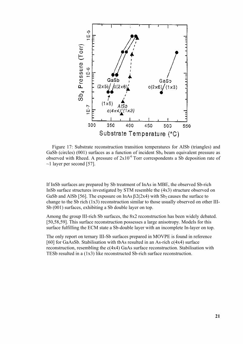
The atomic scale structure under more realistic growth conditions has still to beresolved. Waterman et al. [51]and Sieger [52] et al. have observed a (1x3)-like Rheedpattern for GaSb and AlSb. The GaSb pattern changed into a distinct (2x6) pattern whenthe temperature was increased at reduced Sb flux. STM studies of the III-Sb surfacereconstructions have shown that the observed (1x3) structures must be morecomplex[53]. The most extensive work to investigate the structure of the III-Sb surfaceshas been done by Whitman et al.[49,54] High resolution STM measurements revealedon MBE grown AlSb ,GaSb and InSb that the (1x3) and (2x6) reconstruction consist ofthree single (4x3) phases. On AlSb an α(4x3) ,β(4x3) and γ(4x3) reconstruction withdecreasing substrate temperature was observed. On GaSb the unique GaSb (nx5)reconstruction replaces the γ(4x3) reconstruction in the phase diagram. Similarstructures were observed on InSb. Whitman et al. concluded, that theα(4x3) and β(4x3) surface reconstruction are the dominant ones for III-Sb growth.Unlike the (001) surfaces of III-As,P compounds, that have single-layer As(P)reconstructions under slightly As- (P-) rich conditions, even this least Sb-richreconstruction is composed of a fullplane of Sb atoms covered by an additional 2/3 MLof Sb[51,52,53,53,55].
21
Figure 17: Substrate reconstruction transition temperatures for AlSb (triangles) andGaSb (circles) (001) surfaces as a function of incident Sb4 beam equivalent pressure asobserved with Rheed. A pressure of 2x10⁻⁶ Torr correspondents a Sb deposition rate of~1 layer per second [57].
If InSb surfaces are prepared by Sb treatment of InAs in MBE, the observed Sb-richInSb surface structures investigated by STM resemble the (4x3) structure observed onGaSb and AlSb [56]. The exposure on InAs β2(2x4) with Sb2 causes the surface tochange to the Sb rich (1x3) reconstruction similar to those usually observed on other III-Sb (001) surfaces, exhibiting a Sb double layer on top.
Among the group III-rich Sb surfaces, the 8x2 reconstruction has been widely debated.[50,58,59]. This surface reconstruction possesses a large anisotropy. Models for thissurface fulfilling the ECM state a Sb-double layer with an incomplete In-layer on top.
The only report on ternary III-Sb surfaces prepared in MOVPE is found in reference[60] for GaAsSb. Stabilisation with tbAs resulted in an As-rich c(4x4) surfacereconstruction, resembling the c(4x4) GaAs surface reconstruction. Stabilisation withTESb resulted in a (1x3) like reconstructed Sb-rich surface reconstruction.
22
Figure 18: Ball-and-stick model of the InSb and InAs surface reconstructions[54].
4.3 Antimony on InP in MOCVD and MBE
A literature research reveals that only a few studies have been done to investigate therole of Sb on the InP(001) surface in MOVPE. The majority of papers is related eitherto the properties of Sb as a surfactant in MBE, mediating 2-dimensional growth, or thepassivation of InP surfaces.
Thermal annealing of InP in MBE results in surface decomposition and thusphosphorus depletion at the surface and the formation of metallic indium islands. P.Soukiassan [61] et al. showed that in the presence of an antimony overlayer heating upof InP results in surface restructuring with formation of an thin InSb/InP interface andthe removal of indium islands that formed during prior heating. Thus, Sb was useful as apassivant for InP substrates. Similar results were obtained by Höchst and Rioux[62]. Itwas shown that antimony is helpful as a protection layer when heating up InP in MBEwithout P stabilisation. The Sb coverage saturated after deposition of one ML. Theformation of a thin InSb layer was observed even at room temperature by XPS. On theother hand Sb/InP showed contrary properties compared to As/InP[63] and Sb/GaAs[64]. Thermal desorption studies monitored by RHEED of the later revealed theformation of a strained InAs e.g. GaSb surface layer. RHEED patterns of Sb/InPshowed the existence of two sets of spots corresponding exactly to the bulk latticeconstants of InP and InSb when heated up above 200°C. Rioux and Höchst concludedthat the InSb layer at the interface was relaxed.
23
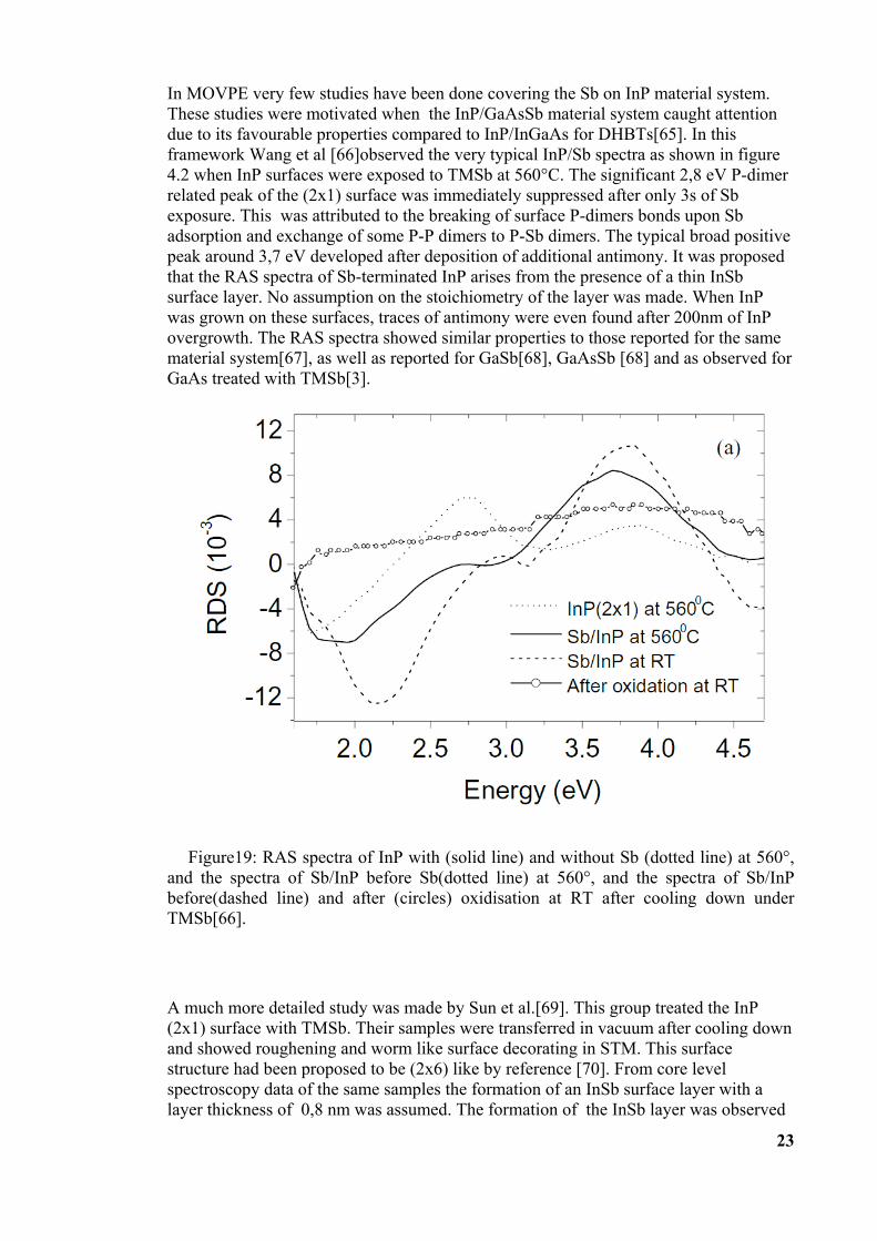
In MOVPE very few studies have been done covering the Sb on InP material system.These studies were motivated when the InP/GaAsSb material system caught attentiondue to its favourable properties compared to InP/InGaAs for DHBTs[65]. In thisframework Wang et al [66]observed the very typical InP/Sb spectra as shown in figure4.2 when InP surfaces were exposed to TMSb at 560°C. The significant 2,8 eV P-dimerrelated peak of the (2x1) surface was immediately suppressed after only 3s of Sbexposure. This was attributed to the breaking of surface P-dimers bonds upon Sbadsorption and exchange of some P-P dimers to P-Sb dimers. The typical broad positivepeak around 3,7 eV developed after deposition of additional antimony. It was proposedthat the RAS spectra of Sb-terminated InP arises from the presence of a thin InSbsurface layer. No assumption on the stoichiometry of the layer was made. When InPwas grown on these surfaces, traces of antimony were even found after 200nm of InPovergrowth. The RAS spectra showed similar properties to those reported for the samematerial system[67], as well as reported for GaSb[68], GaAsSb [68] and as observed forGaAs treated with TMSb[3].
Figure19: RAS spectra of InP with (solid line) and without Sb (dotted line) at 560°,and the spectra of Sb/InP before Sb(dotted line) at 560°, and the spectra of Sb/InPbefore(dashed line) and after (circles) oxidisation at RT after cooling down underTMSb[66].
A much more detailed study was made by Sun et al.[69]. This group treated the InP(2x1) surface with TMSb. Their samples were transferred in vacuum after cooling downand showed roughening and worm like surface decorating in STM. This surfacestructure had been proposed to be (2x6) like by reference [70]. From core levelspectroscopy data of the same samples the formation of an InSb surface layer with alayer thickness of 0,8 nm was assumed. The formation of the InSb layer was observed
24
in a temperature range from 450°C to 600°C. No temperature dependence of the InSblayer thickness was found and thus proposed, that desorption in this temperature rangewas negligible.
4.4 Strain induced surface melting
The increasing interest in quantum dot epitaxy during the last decade led to thesystematically investigation of highly strained layers. It is commonly accepted that theenergetic of strain relief plays the key role in the understanding of those phenomena.For instance only systems with a lattice mismatch ≥ 2 % show the Stranski-Krastanovgrowth mode [26] and can be used to grow quantum dots: after the formation of awetting layer 3-dimensional islands form on top.
A novel approach to treat the behaviour of strained heteroepitaxial layers wasintroduced by Bottomley [23,24]. Bottomley proposed that the strain in the layer canbe interpreted as a hydrostatic pressure. Therefore, the free energy of the surface has tobe calculated from the Gibbs free energy, and not as generally assumed from theHelmholz free energy. This claim was supposed by prediction of melting point ofseveral semiconductors. He calculated that the large epitaxial stress of InAs on GaAscan melt the InAs film at a certain temperature below the InAs melting point. Thiswould lead to the formation of a quasi liquid surface melt, which is characterised by theloss of long range crystalline order at the surface, This is only possible , if the energyapplied by the strain is sufficient to melt the surface layer, but is smaller than thedislocation energy. Elsewise dislocation would compensate the strain., the layer wouldnot be strained anymore, and thus the material would solidify. A behaviour found onGaAs/InAs interfaces, where not QD’s form but dislocations. Since this theory plays animportant role in the understanding of Sb segregation in InP, the underlyingthermodynamic model will be explained in the following section in more detail.Additionally the consequences which are important for the explanation of the observedphenomena in Sb segregation will be pointed out as well.
4.4.1 Thermodynamic model
The key assumption of Bottomley was that the Gibbs free energies the important valueto be considered for strained materials instead of the Helmholtz free energy (as wasproposed by Gibbs ironically himself) [27,28,29].
Thus, classical thermodynamics textbooks will use the Helmholtz free energy
PdVSdTdF −−= (1)
to calculate the free energy density of isotropic and cubic media under hydrostaticstress. Integrating of above equation at constant T gives:
25
∫ ∫ −=−== ijijVdVP
VdFE εσ
21 (2)
σij and εij are the stress and strain tensors. Applying Hook’s Law lead to the free energydensity E :
21211 )2(
23 εccE +−= (3)
with cij being the stiffness tensor elements and ε2 the strain. According to this equationthe free energy density would be quadratic in the strain.
Bottomley argued that the Helmholtz free energy is not the right term to describe asystem under hydrostatic pressure. He pointed out that a system under stress is atconstant P and T, instead of constant V and T. Instead of the Helmholtz free energy theGibbs free energy has to be used to calculate the free energy density.
VdPSdTdG +−= (4)
Following this approach the free energy density at constant T is then given by:
∫ ∫ −==== ijijPV
VdPVdFE δσ
31 (5)
Therefore the free energy and the pressure are identical. Applying Hook’s law toequation (5) gives
ε)2( ijij ccE +−= (6)
In this case the free energy would be linear, and not quadratic in the strain and haveopposite sign.
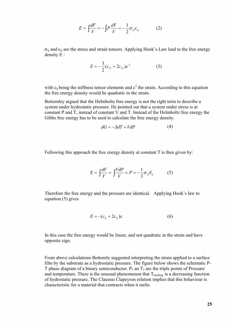
From above calculations Bottomly suggested interpreting the strain applied to a surfacefilm by the substrate as a hydrostatic pressure. The figure below shows the schematic P-T phase diagram of a binary semiconductor. P3 an T3 are the triple points of Pressureand temperature. There is the unusual phenomenon that Tmelting is a decreasing functionof hydrostatic pressure. The Clausius Clapeyron relation implies that this behaviour ischaracteristic for a material that contracts when it melts.
26
Figure 20: Schematic P-T phase diagram of a zincblende semiconductor.
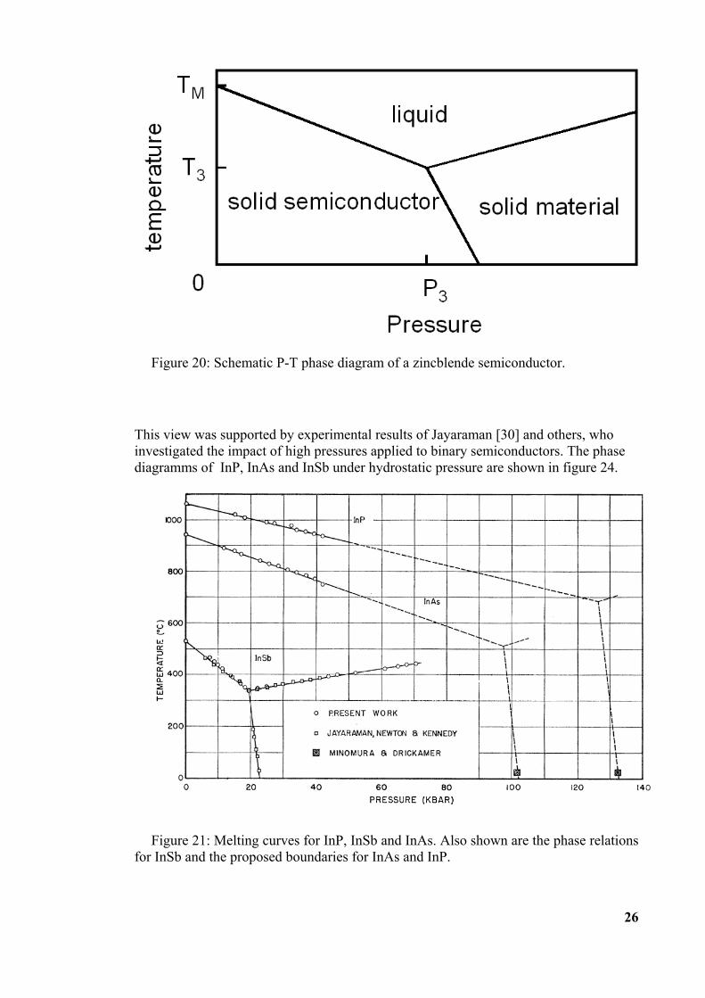
This view was supported by experimental results of Jayaraman [30] and others, whoinvestigated the impact of high pressures applied to binary semiconductors. The phasediagramms of InP, InAs and InSb under hydrostatic pressure are shown in figure 24.
Figure 21: Melting curves for InP, InSb and InAs. Also shown are the phase relationsfor InSb and the proposed boundaries for InAs and InP.
27
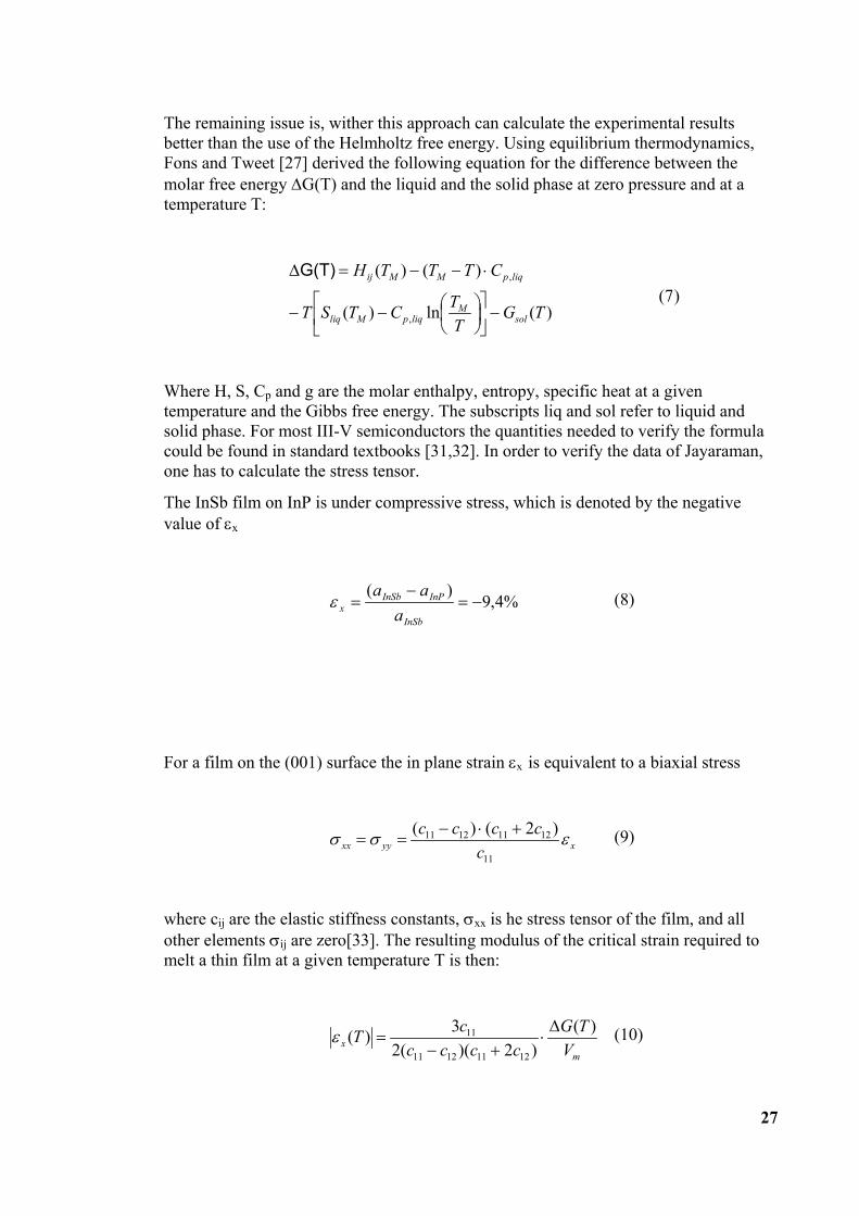
The remaining issue is, wither this approach can calculate the experimental resultsbetter than the use of the Helmholtz free energy. Using equilibrium thermodynamics,Fons and Tweet [27] derived the following equation for the difference between themolar free energy ∆G(T) and the liquid and the solid phase at zero pressure and at atemperature T:
)(ln)(
)()(
,
,
TGT
TCTST
CTTTH
solM
liqpMliq
liqpMMij
−
−−
⋅−−=∆G(T) (7)
Where H, S, Cp and g are the molar enthalpy, entropy, specific heat at a giventemperature and the Gibbs free energy. The subscripts liq and sol refer to liquid andsolid phase. For most III-V semiconductors the quantities needed to verify the formulacould be found in standard textbooks [31,32]. In order to verify the data of Jayaraman,one has to calculate the stress tensor.
The InSb film on InP is under compressive stress, which is denoted by the negativevalue of εx
%4,9)(
−=−
=InSb
InPInSbx a
aaε (8)
For a film on the (001) surface the in plane strain εx is equivalent to a biaxial stress
xyyxx ccccc εσσ
11
12111211 )2()( +⋅−== (9)
where cij are the elastic stiffness constants, σxx is he stress tensor of the film, and allother elements σij are zero[33]. The resulting modulus of the critical strain required tomelt a thin film at a given temperature T is then:
mx V
TGcccc
cT )()2)((2
3)(12111211
11 ∆⋅
+−=ε (10)
28
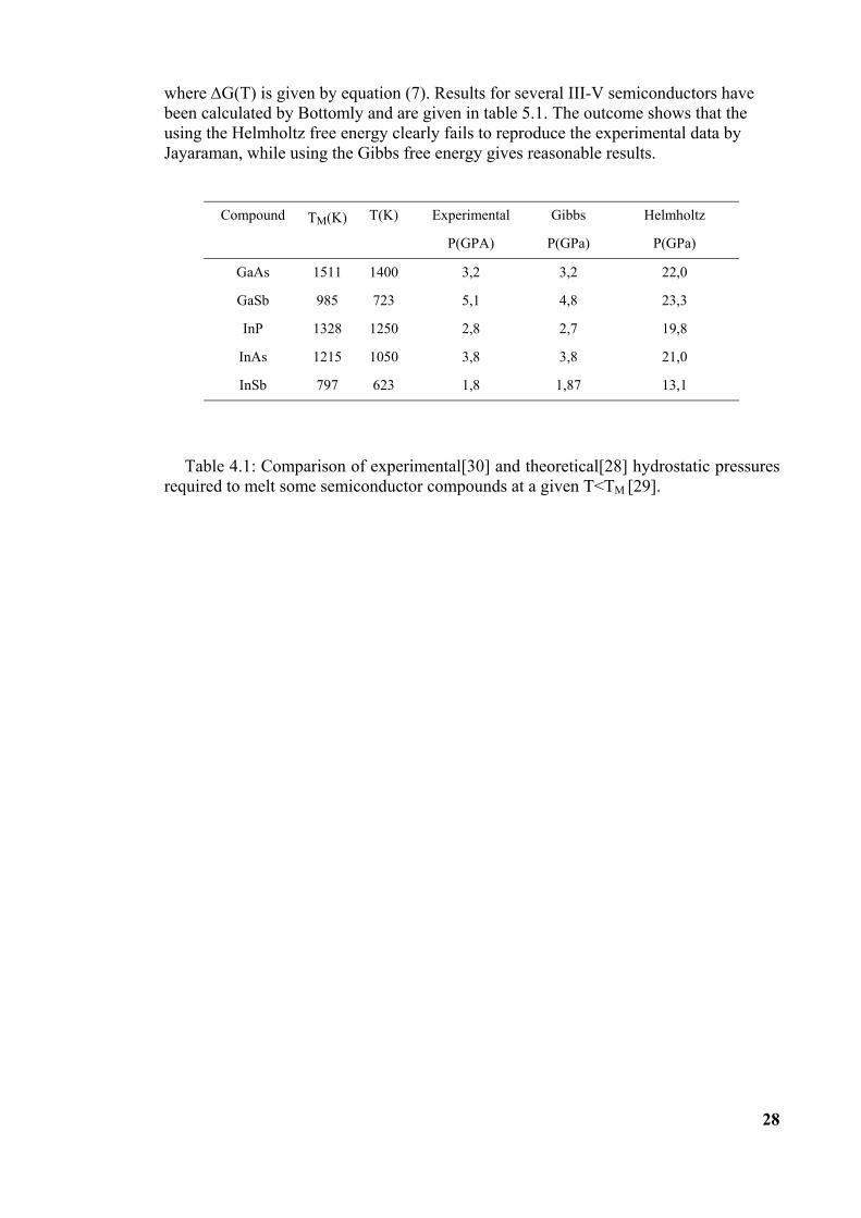
where ∆G(T) is given by equation (7). Results for several III-V semiconductors havebeen calculated by Bottomly and are given in table 5.1. The outcome shows that theusing the Helmholtz free energy clearly fails to reproduce the experimental data byJayaraman, while using the Gibbs free energy gives reasonable results.
Compound TM(K) T(K) Experimental
P(GPA)
Gibbs
P(GPa)
Helmholtz
P(GPa)
GaAs 1511 1400 3,2 3,2 22,0
GaSb 985 723 5,1 4,8 23,3
InP 1328 1250 2,8 2,7 19,8
InAs 1215 1050 3,8 3,8 21,0
InSb 797 623 1,8 1,87 13,1
Table 4.1: Comparison of experimental[30] and theoretical[28] hydrostatic pressuresrequired to melt some semiconductor compounds at a given T<TM [29].
29
5 Experimental
All growth was performed on epi-ready InP substrates, either undoped orsemiinsulating. As precursors phosphine, TMSb and TMIn were used. The substratewas deoxidised by heating in PH3 ambient up to 700°C.
Phosphine decomposes at temperatures between 673 K (5%) and 900 k (100%) and isavailable at good quality. Additionally the pyrolysis of phosphine produces hydrogen,supporting the oxide while heating up.
TMSb was used as Sb precursor. TMSb is the Sb source with the highest vapourpressure, and is the only precursor among the large variety of tested precursors, that iscommercially avail able. In the temperature range used it is reported to be decomposedfrom 35 % at 520°C to 100 % at 570°C and above [10,20].
The decomposition of the used precursors with regard to the temperature is shown inchapter 3.2, figure 8.
The experiments were performed in an Aixtron-like horizontal double wall quartzreactor with three purged strain free windows using two reflectance anisotropyspectrometer (RAS) allowing simultaneous time and energy resolved in-situmeasurements with a resolution below 1 s [38]. The carrier gas was 3 l/min at 10 kPa ofpurified hydrogen, 200 Pa Phosphine (PH3 ) and 2 Pa trimethyl-antimony (TMSb) wereused as group V precursors until otherwise noted. Typically trimethyl-indium (TMIn)was used as group III precursors. The resulting InP growth rate was 1 µm/h, were usedfor monitoring. The experiments were monitored by two in-situ RAS systems asdescribed in chapter 4. After growth the samples were analysed ex-situ using a DigitalInstruments Atomic Force Microscopy (AFM). High resolution X-Ray Diffraction(XRD) was performed with a Philips MRD diffractometer. A Takagi-Taupin algorithmwas used for XRD rocking curve simulations. Secondary Ion Mass Spectroscopy(SIMS) was done with a CAMECA SIMS at RTG Microanalyse GmbH, Adlershof.
5.1 Monitoring Antimony in MOCVD
Once a III-V surface is treated with antimony, a distinct feature is visible. Noticeable isthe broad positive peak around 3,8 eV similar to published spectra [71]. Thus thegeneral shape of the spectra is similar to RAS spectra of GaAs contaminated with Sb[66] and also for GaSb [68,72] and GaAsSb [73,74]. They all have the samecharacteristic peak around 3,8 eV in common. Therefore the 3,8 eV peak was related tothe presence of Sb on the surface. Therefore a dynamic study of Sb terminated InPsurfaces including exchange and interface formation processes were monitored at 3,8eV
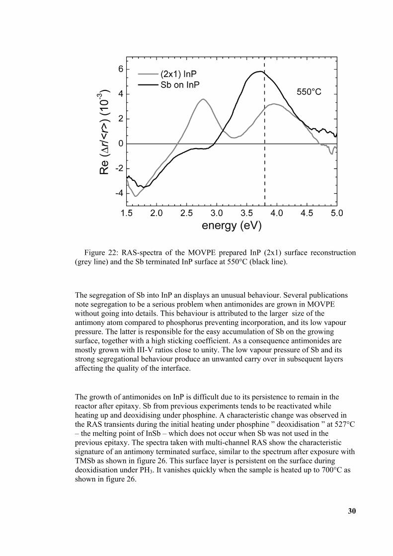
30
Figure 22: RAS-spectra of the MOVPE prepared InP (2x1) surface reconstruction(grey line) and the Sb terminated InP surface at 550°C (black line).
The segregation of Sb into InP an displays an unusual behaviour. Several publicationsnote segregation to be a serious problem when antimonides are grown in MOVPEwithout going into details. This behaviour is attributed to the larger size of theantimony atom compared to phosphorus preventing incorporation, and its low vapourpressure. The latter is responsible for the easy accumulation of Sb on the growingsurface, together with a high sticking coefficient. As a consequence antimonides aremostly grown with III-V ratios close to unity. The low vapour pressure of Sb and itsstrong segregational behaviour produce an unwanted carry over in subsequent layersaffecting the quality of the interface.
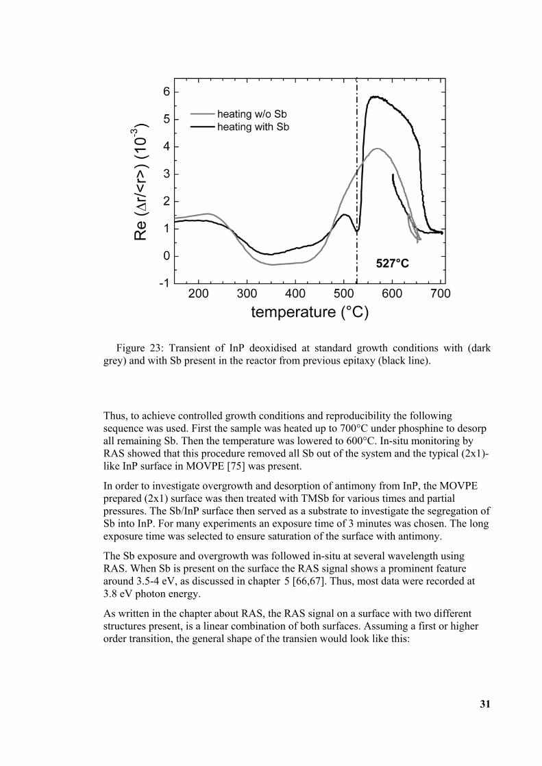
The growth of antimonides on InP is difficult due to its persistence to remain in thereactor after epitaxy. Sb from previous experiments tends to be reactivated whileheating up and deoxidising under phosphine. A characteristic change was observed inthe RAS transients during the initial heating under phosphine ” deoxidisation ” at 527°C– the melting point of InSb – which does not occur when Sb was not used in theprevious epitaxy. The spectra taken with multi-channel RAS show the characteristicsignature of an antimony terminated surface, similar to the spectrum after exposure withTMSb as shown in figure 26. This surface layer is persistent on the surface duringdeoxidisation under PH3. It vanishes quickly when the sample is heated up to 700°C asshown in figure 26.
31
Figure 23: Transient of InP deoxidised at standard growth conditions with (darkgrey) and with Sb present in the reactor from previous epitaxy (black line).
Thus, to achieve controlled growth conditions and reproducibility the followingsequence was used. First the sample was heated up to 700°C under phosphine to desorpall remaining Sb. Then the temperature was lowered to 600°C. In-situ monitoring byRAS showed that this procedure removed all Sb out of the system and the typical (2x1)-like InP surface in MOVPE [75] was present.
In order to investigate overgrowth and desorption of antimony from InP, the MOVPEprepared (2x1) surface was then treated with TMSb for various times and partialpressures. The Sb/InP surface then served as a substrate to investigate the segregation ofSb into InP. For many experiments an exposure time of 3 minutes was chosen. The longexposure time was selected to ensure saturation of the surface with antimony.
The Sb exposure and overgrowth was followed in-situ at several wavelength usingRAS. When Sb is present on the surface the RAS signal shows a prominent featurearound 3.5-4 eV, as discussed in chapter 5 [66,67]. Thus, most data were recorded at3.8 eV photon energy.
As written in the chapter about RAS, the RAS signal on a surface with two differentstructures present, is a linear combination of both surfaces. Assuming a first or higherorder transition, the general shape of the transien would look like this:
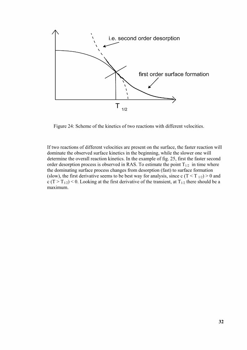
32
If two reactions of different velocities are present on the surface, the faster reaction willdominate the observed surface kinetics in the beginning, while the slower one willdetermine the overall reaction kinetics. In the example of fig. 25, first the faster secondorder desorption process is observed in RAS. To estimate the point T1/2 in time wherethe dominating surface process changes from desorption (fast) to surface formation(slow), the first derivative seems to be best way for analysis, since c (T < T 1/2) > 0 andc (T > T1/2) < 0. Looking at the first derivative of the transient, at T1/2 there should be amaximum.
Figure 24: Scheme of the kinetics of two reactions with different velocities.
33
6 Adsorption and desorption of Sb from InPsurfaces in MOCVD
In order to understand the various surface transitions observed by RAS duringadsorption and desorption an understanding of the properties of the Sb/InP surface isnecessary.
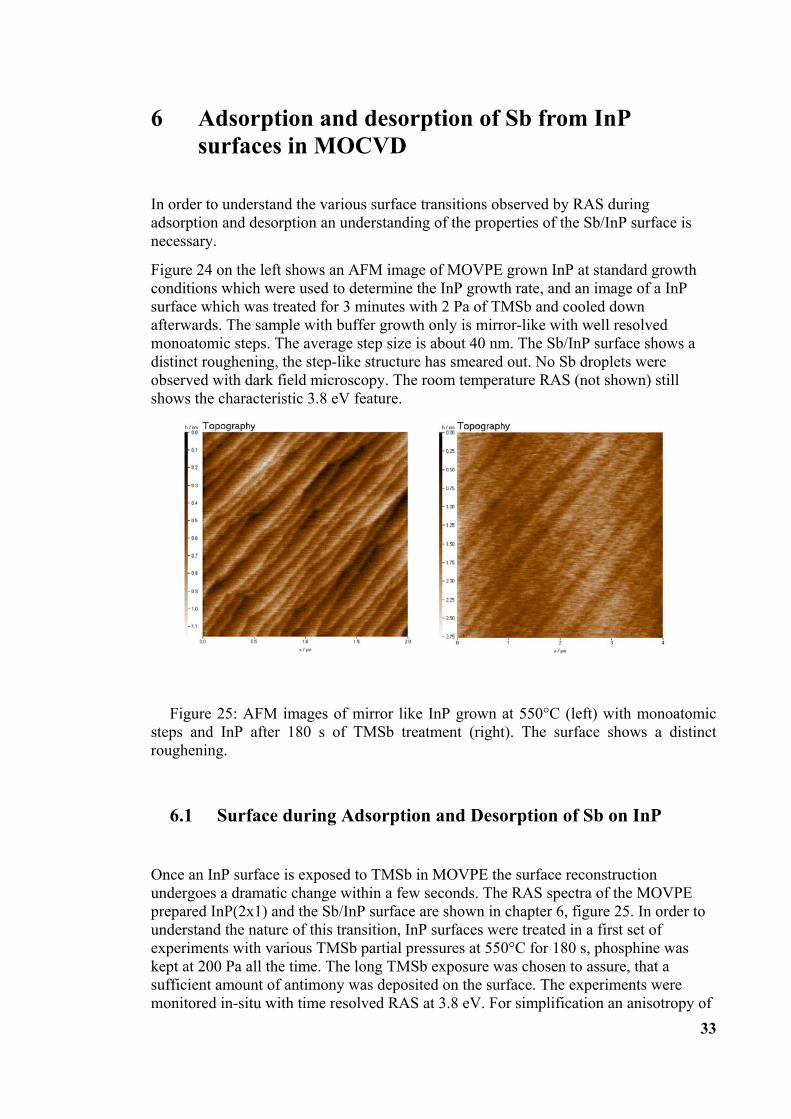
Figure 24 on the left shows an AFM image of MOVPE grown InP at standard growthconditions which were used to determine the InP growth rate, and an image of a InPsurface which was treated for 3 minutes with 2 Pa of TMSb and cooled downafterwards. The sample with buffer growth only is mirror-like with well resolvedmonoatomic steps. The average step size is about 40 nm. The Sb/InP surface shows adistinct roughening, the step-like structure has smeared out. No Sb droplets wereobserved with dark field microscopy. The room temperature RAS (not shown) stillshows the characteristic 3.8 eV feature.
Figure 25: AFM images of mirror like InP grown at 550°C (left) with monoatomicsteps and InP after 180 s of TMSb treatment (right). The surface shows a distinctroughening.
6.1 Surface during Adsorption and Desorption of Sb on InP
Once an InP surface is exposed to TMSb in MOVPE the surface reconstructionundergoes a dramatic change within a few seconds. The RAS spectra of the MOVPEprepared InP(2x1) and the Sb/InP surface are shown in chapter 6, figure 25. In order tounderstand the nature of this transition, InP surfaces were treated in a first set ofexperiments with various TMSb partial pressures at 550°C for 180 s, phosphine waskept at 200 Pa all the time. The long TMSb exposure was chosen to assure, that asufficient amount of antimony was deposited on the surface. The experiments weremonitored in-situ with time resolved RAS at 3.8 eV. For simplification an anisotropy of
34
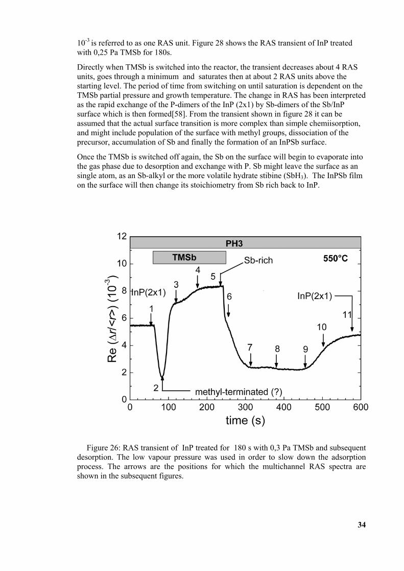
10-3 is referred to as one RAS unit. Figure 28 shows the RAS transient of InP treatedwith 0,25 Pa TMSb for 180s.
Directly when TMSb is switched into the reactor, the transient decreases about 4 RASunits, goes through a minimum and saturates then at about 2 RAS units above thestarting level. The period of time from switching on until saturation is dependent on theTMSb partial pressure and growth temperature. The change in RAS has been interpretedas the rapid exchange of the P-dimers of the InP (2x1) by Sb-dimers of the Sb/InPsurface which is then formed[58]. From the transient shown in figure 28 it can beassumed that the actual surface transition is more complex than simple chemiisorption,and might include population of the surface with methyl groups, dissociation of theprecursor, accumulation of Sb and finally the formation of an InPSb surface.
Once the TMSb is switched off again, the Sb on the surface will begin to evaporate intothe gas phase due to desorption and exchange with P. Sb might leave the surface as ansingle atom, as an Sb-alkyl or the more volatile hydrate stibine (SbH3). The InPSb filmon the surface will then change its stoichiometry from Sb rich back to InP.
Figure 26: RAS transient of InP treated for 180 s with 0,3 Pa TMSb and subsequentdesorption. The low vapour pressure was used in order to slow down the adsorptionprocess. The arrows are the positions for which the multichannel RAS spectra areshown in the subsequent figures.
35
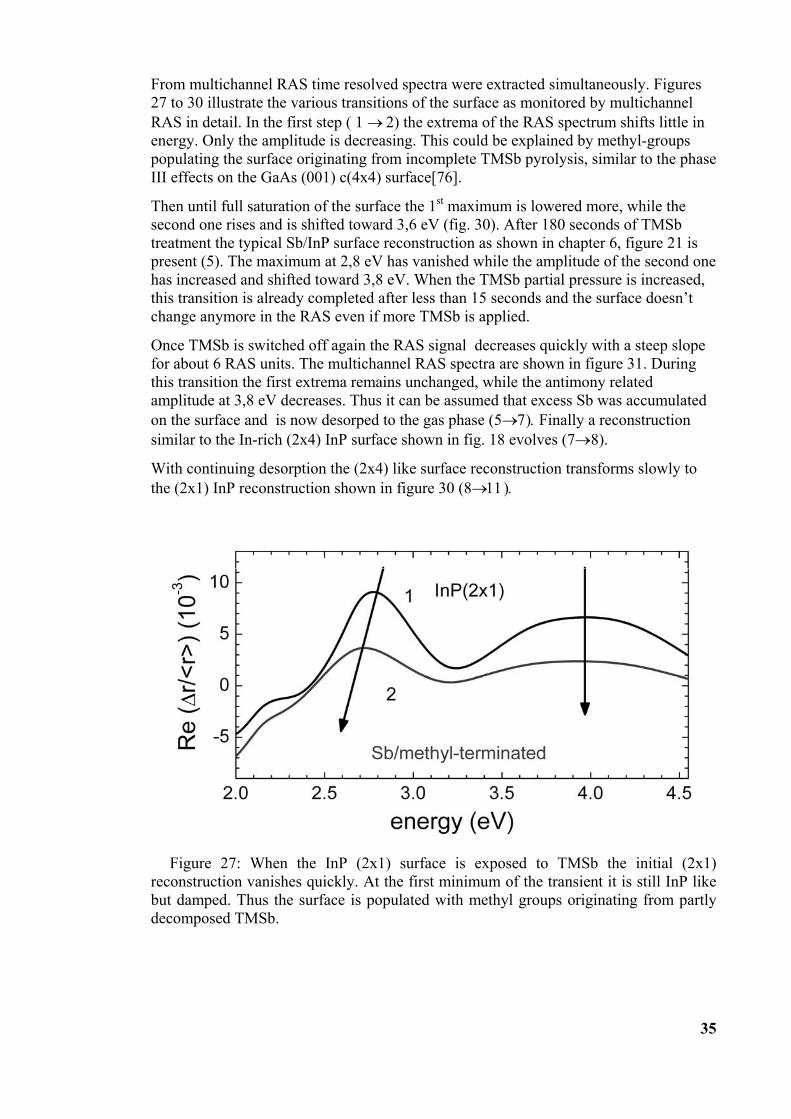
From multichannel RAS time resolved spectra were extracted simultaneously. Figures27 to 30 illustrate the various transitions of the surface as monitored by multichannelRAS in detail. In the first step ( 1 → 2) the extrema of the RAS spectrum shifts little inenergy. Only the amplitude is decreasing. This could be explained by methyl-groupspopulating the surface originating from incomplete TMSb pyrolysis, similar to the phaseIII effects on the GaAs (001) c(4x4) surface[76].
Then until full saturation of the surface the 1st maximum is lowered more, while thesecond one rises and is shifted toward 3,6 eV (fig. 30). After 180 seconds of TMSbtreatment the typical Sb/InP surface reconstruction as shown in chapter 6, figure 21 ispresent (5). The maximum at 2,8 eV has vanished while the amplitude of the second onehas increased and shifted toward 3,8 eV. When the TMSb partial pressure is increased,this transition is already completed after less than 15 seconds and the surface doesn’tchange anymore in the RAS even if more TMSb is applied.
Once TMSb is switched off again the RAS signal decreases quickly with a steep slopefor about 6 RAS units. The multichannel RAS spectra are shown in figure 31. Duringthis transition the first extrema remains unchanged, while the antimony relatedamplitude at 3,8 eV decreases. Thus it can be assumed that excess Sb was accumulatedon the surface and is now desorped to the gas phase (5→7). Finally a reconstructionsimilar to the In-rich (2x4) InP surface shown in fig. 18 evolves (7→8).
With continuing desorption the (2x4) like surface reconstruction transforms slowly tothe (2x1) InP reconstruction shown in figure 30 (8→11).
Figure 27: When the InP (2x1) surface is exposed to TMSb the initial (2x1)reconstruction vanishes quickly. At the first minimum of the transient it is still InP likebut damped. Thus the surface is populated with methyl groups originating from partlydecomposed TMSb.
36
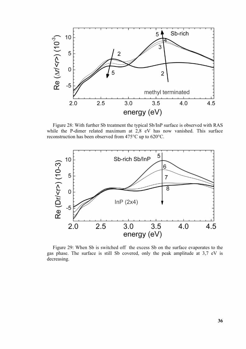
Figure 28: With further Sb treatment the typical Sb/InP surface is observed with RASwhile the P-dimer related maximum at 2,8 eV has now vanished. This surfacereconstruction has been observed from 475°C up to 620°C.
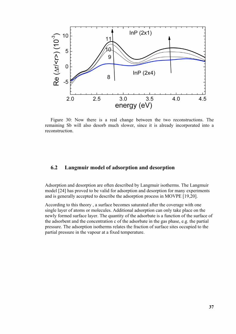
Figure 29: When Sb is switched off the excess Sb on the surface evaporates to thegas phase. The surface is still Sb covered, only the peak amplitude at 3,7 eV isdecreasing.
37
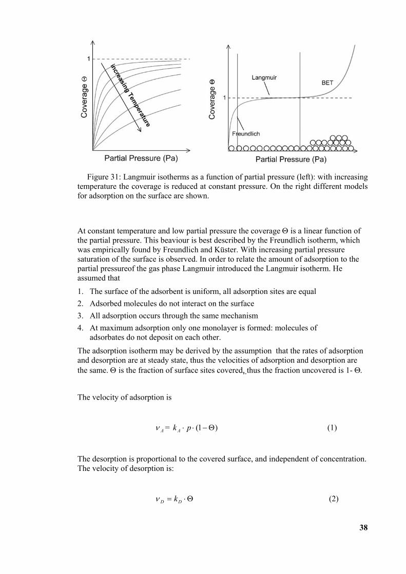
Figure 30: Now there is a real change between the two reconstructions. Theremaining Sb will also desorb much slower, since it is already incorporated into areconstruction.
6.2 Langmuir model of adsorption and desorption
Adsorption and desorption are often described by Langmuir isotherms. The Langmuirmodel [24] has proved to be valid for adsorption and desorption for many experimentsand is generally accepted to describe the adsorption process in MOVPE [19,20].
According to this theory , a surface becomes saturated after the coverage with onesingle layer of atoms or molecules. Additional adsorption can only take place on thenewly formed surface layer. The quantity of the adsorbate is a function of the surface ofthe adsorbent and the concentration c of the adsorbate in the gas phase, e.g. the partialpressure. The adsorption isotherms relates the fraction of surface sites occupied to thepartial pressure in the vapour at a fixed temperature.
38
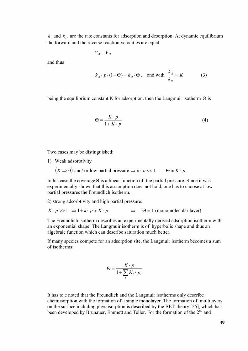
Figure 31: Langmuir isotherms as a function of partial pressure (left): with increasingtemperature the coverage is reduced at constant pressure. On the right different modelsfor adsorption on the surface are shown.
At constant temperature and low partial pressure the coverage Θ is a linear function ofthe partial pressure. This beaviour is best described by the Freundlich isotherm, whichwas empirically found by Freundlich and Küster. With increasing partial pressuresaturation of the surface is observed. In order to relate the amount of adsorption to thepartial pressureof the gas phase Langmuir introduced the Langmuir isotherm. Heassumed that
1. The surface of the adsorbent is uniform, all adsorption sites are equal2. Adsorbed molecules do not interact on the surface3. All adsorption occurs through the same mechanism4. At maximum adsorption only one monolayer is formed: molecules of
adsorbates do not deposit on each other.
The adsorption isotherm may be derived by the assumption that the rates of adsorptionand desorption are at steady state, thus the velocities of adsorption and desorption arethe same. Θ is the fraction of surface sites covered, thus the fraction uncovered is 1- Θ.
The velocity of adsorption is
Aν = )1( Θ−⋅⋅ pk A (1)
The desorption is proportional to the covered surface, and independent of concentration.The velocity of desorption is:
Θ⋅= DD kν (2)
39
Ak and Dk are the rate constants for adsorption and desorption. At dynamic equilibriumthe forward and the reverse reaction velocities are equal:
DA νν =
and thus
Θ⋅=Θ−⋅⋅ DA kpk )1( . and with Kkk
D
A = (3)
being the equilibrium constant K for adsorption. then the Langmuir isotherm Θ is
=ΘpK
pK⋅+
⋅1
(4)
Two cases may be distinguished:
1) Weak adsorbtivity
( )0⇒K and/ or low partial pressure 1<<⋅⇒ pk pK ⋅≈Θ
In his case the coverage Θ is a linear function of the partial pressure. Since it wasexperimentally shown that this assumption does not hold, one has to choose at lowpartial pressures the Freundlich isotherm.
2) strong adsorbtivity and high partial pressure:
1>>⋅ pK pKpk ⋅≈⋅+⇒ 1 ⇒ 1=Θ (monomolecular layer)
The Freundlich isotherm describes an experimentally derived adsorption isotherm withan exponential shape. The Langmuir isotherm is of hyperbolic shape and thus analgebraic function which can describe saturation much better.
If many species compete for an adsorption site, the Langmuir isotherm becomes a sumof isotherms:
∑ ⋅+⋅
=Θ
iii pK
pK1
It has to e noted that the Freundlich and the Langmuir isotherms only describechemiisorption with the formation of a single monolayer. The formation of multilayerson the surface including physiisorption is described by the BET-theory [25], which hasbeen developed by Brunauer, Emmett and Teller. For the formation of the 2nd and
40
further layers Van-der-Waals forces are responsible. They are supported by high vapourpressure and low temperatures.
The desorption process is the opposite of adsorption, whereby some of the adsorbedsubstance is released back to the gas phase. It is usually trated in the same way asadsorption. Assumed is that1. Particles who have once reached the transition state do not return to the initial
state.2. The energy levels of the initial state follow a Boltzmann distribution and of
the transition state are statistically distributed.3. The velocity of reaction is the same for all particles
The desorption ratet
R∂∂−
=θ is measured as a function of time or temperature.
The rapid change in the RAS signal implies that the surface gets rapidly covered byantimony. Shurtleff et al [77] suggested the following form of the Langmuir equationfor the adsorption of TMSb on InGaP:
Θ−Θ−Θ−⋅=Θ
iDASb kkkPdtd )1( (6.1)
where Θ denotes the concentration of Sb on the surface, Ak is the adsorption constantfor Sb and Dk is the desorption constant for Sb. An constant ik for incorporation of Sbinto InP was added .
For the start of adsorption of antimony on the surface the initial slope of the adsorptioncurve is given by:
ASb kPdtd
⋅=Θ (6.2)
A higher TMSb partial pressure will then result in a steeper transient and thus a fastersaturation of the surface with antimony, which agrees well with the RAS data shown infigure 31 on the right.
A simple expression for the desorption isotherm can be obtained assuming that P and Sbas group V elements both occupy the same surface sites. The P-isotherm will then beexpressed in relation to the Sb coverage to be Sbθ−1 . If the surface is completelycovered with antimony and thus in the steady state with no further Sb uptake, thedesorption of Sb from the surface will then be described by the coverage and the kinetic
41
constants. The experiments have shown that full saturation with Sb is already reachedwhen more than 0,25 Pa TMSb are applied for 180 s. Thus
)( id kkdtd
+−=θ (6.3)
This implies that for PSb > (kd + ki) the slope of the transient of adsorption will alwaysbe steeper than the slope of the transient for desorption. This is observed for any partialpressure chosen.
A simple equation for adsorption of Sb on InP can be obtained when the Langmuirequation is integrated for Θ (0)=0 and PSbka > (kd+ki):
Adsorption: )1( at
e τθ−
−= with aSba kP/(1=τ ) (6.4)
Integration of the Langmuir equation for Θ (0) = 1 and PSb = 0 delivers an equation fordesorption from a completely saturated surface:
Desorption: dt
e τθ−
= with )(1 idd kk −=τ (6.5)
τi and τd are the time constants for adsorption and desorption transients respectively.Several results for ka and kd have been obtained by fitting RAS transients taken atdifferent temperatures with the required exponential functions and calculating thereaction rate constants from the fit parameters τa and τd.
6.3 Adsorption and desorption of Sb on InP
In order to investigate the temperature dependence of Sb adsorption and desorption, thesamples were treated for 180s with TMSb at various temperatures. After switching offthe TMSb the sample was purged with phosphine until the antimony was desorbed fromthe surface and the InP(2x1) reconstruction returned. The actual condition of the surfacewas monitored with RAS at 3,8 eV. Once the RAS transient had reached its startinglevel again, the temperature was increased by 20°C and a buffer was grown with 0.5 PaTMIn. Afterward the InP was exposed again to Sb. In-situ monitoring with RAS insuredthat no Sb had been activated by heating up from the susceptor, the linertube or thereactor walls and the InP(2x1) surface was present again. The RAS transients for 520°C,540°C, 560°C, 580°C, 600°C, 620°C are displayed in fig. 28. The desorption transient
42
of Sb shows a similar behaviour than the one of overgrowth of antimony with InP (fig.29), but an opposite temperature behaviour.
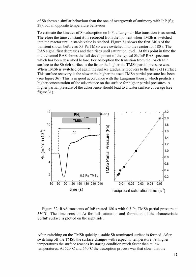
To estimate the kinetics of Sb adsorption on InP, a Langmuir like transition is assumed.Therefore the time constant ∆t is recorded from the moment when TMSb is switchedinto the reactor until a stable value is reached. Figure 31 shows the first 240 s of thetransient shown before as 0,3 Pa TMSb were switched into the reactor for 180 s. TheRAS signal first decreases and then rises until saturation level.. At this point in time themultichannel RAS shows the full development of the typical Sb/InP RAS spectrumwhich has been described before. For adsorption the transition from the P-rich InPsurface to the Sb rich surface is the faster the higher the TMSb partial pressure was.When TMSb is switched of again the surface gradually recovers to the InP(2x1) surface.This surface recovery is the slower the higher the used TMSb partial pressure has been(see figure 36). This is in good accordance with the Langmuir theory, which predicts ahigher concentration of the adsorbence on the surface for higher partial pressures. Ahigher partial pressure of the adsorbence should lead to a faster surface coverage (seefigure 31).
Figure 32: RAS transients of InP treated 180 s with 0.3 Pa TMSb partial pressure at550°C. The time constant ∆t for full saturation and formation of the characteristicSb/InP surface is plotted on the right side.
After switching on the TMSb quickly a stable Sb terminated surface is formed. Afterswitching off the TMSb the surface changes with respect to temperature: At highertemperatures the surface reaches its staring condition much faster than at lowtemperatures. At 520°C and 540°C the desorption process was that slow, that the
43
beforehand chosen time to record it was insufficient.
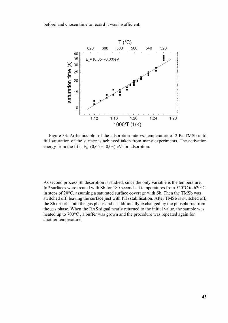
Figure 33: Arrhenius plot of the adsorption rate vs. temperature of 2 Pa TMSb untilfull saturation of the surface is achieved taken from many experiments. The activationenergy from the fit is Ea=(0,65 ± 0,03) eV for adsorption.
As second process Sb desorption is studied, since the only variable is the temperature.InP surfaces were treated with Sb for 180 seconds at temperatures from 520°C to 620°Cin steps of 20°C, assuming a saturated surface coverage with Sb. Then the TMSb wasswitched off, leaving the surface just with PH3 stabilisation. After TMSb is switched off,the Sb desorbs into the gas phase and is additionally exchanged by the phosphorus fromthe gas phase. When the RAS signal nearly returned to the initial value, the sample washeated up to 700°C , a buffer was grown and the procedure was repeated again foranother temperature.
44
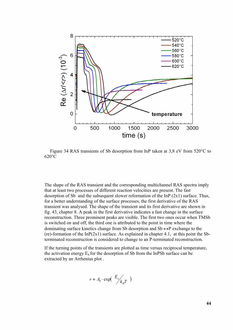
Figure 34 RAS transients of Sb desorption from InP taken at 3,8 eV from 520°C to620°C
The shape of the RAS transient and the corresponding multichannel RAS spectra implythat at least two processes of different reaction velocities are present. The fastdesorption of Sb and the subsequent slower reformation of the InP (2x1) surface. Thus,for a better understanding of the surface processes, the first derivative of the RAStransient was analysed. The shape of the transient and its first derivative are shown infig. 43, chapter 8. A peak in the first derivative indicates a fast change in the surfacereconstruction. Three prominent peaks are visible. The first two ones occur when TMSbis switched on and off, the third one is attributed to the point in time where thedominating surface kinetics change from Sb desorption and Sb ↔P exchange to the(re)-formation of the InP(2x1) surface. As explained in chapter 4.1, at this point the Sb-terminated reconstruction is considered to change to an P-terminated reconstruction.
If the turning points of the transients are plotted as time versus reciprocal temperature,the activation energy Ea for the desorption of Sb from the InPSb surface can beextracted by an Arrhenius plot .
( )TkEAr
B
aexp0 ⋅≈
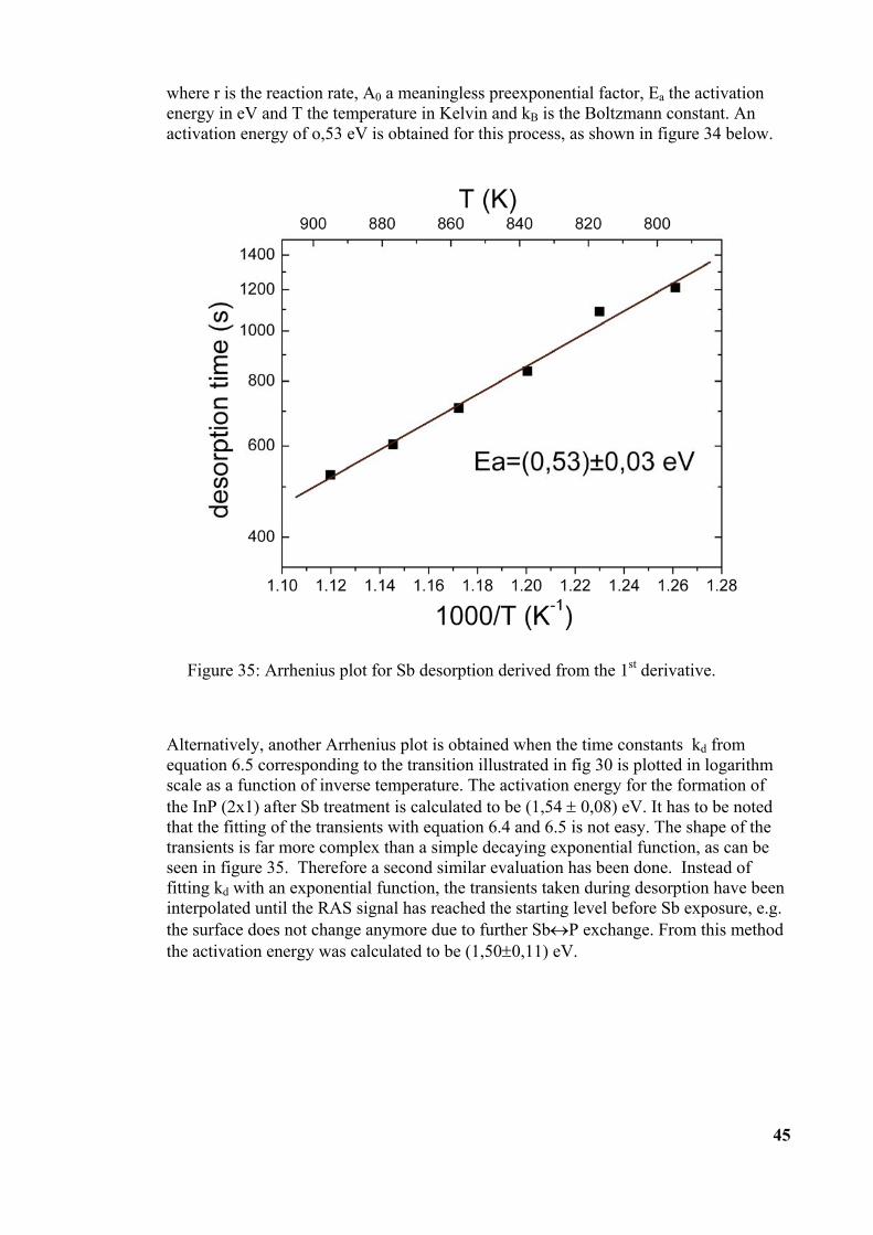
45
where r is the reaction rate, A0 a meaningless preexponential factor, Ea the activationenergy in eV and T the temperature in Kelvin and kB is the Boltzmann constant. Anactivation energy of o,53 eV is obtained for this process, as shown in figure 34 below.
Figure 35: Arrhenius plot for Sb desorption derived from the 1st derivative.
Alternatively, another Arrhenius plot is obtained when the time constants kd fromequation 6.5 corresponding to the transition illustrated in fig 30 is plotted in logarithmscale as a function of inverse temperature. The activation energy for the formation ofthe InP (2x1) after Sb treatment is calculated to be (1,54 ± 0,08) eV. It has to be notedthat the fitting of the transients with equation 6.4 and 6.5 is not easy. The shape of thetransients is far more complex than a simple decaying exponential function, as can beseen in figure 35. Therefore a second similar evaluation has been done. Instead offitting kd with an exponential function, the transients taken during desorption have beeninterpolated until the RAS signal has reached the starting level before Sb exposure, e.g.the surface does not change anymore due to further Sb↔P exchange. From this methodthe activation energy was calculated to be (1,50±0,11) eV.
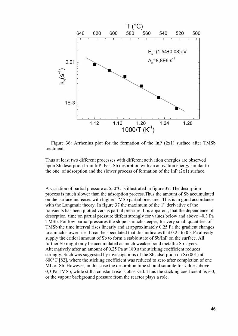
46
Figure 36: Arrhenius plot for the formation of the InP (2x1) surface after TMSbtreatment.
Thus at least two different processes with different activation energies are observedupon Sb desorption from InP: Fast Sb desorption with an activation energy similar tothe one of adsorption and the slower process of formation of the InP (2x1) surface.
A variation of partial pressure at 550°C is illustrated in figure 37. The desorptionprocess is much slower than the adsorption process.Thus the amount of Sb accumulatedon the surface increases with higher TMSb partial pressure. This is in good accordancewith the Langmuir theory. In figure 37 the maximum of the 1st derivative of thetransients has been plotted versus partial pressure. It is apparent, that the dependence ofdesorption time on partial pressure differs strongly for values below and above ~0,3 PaTMSb. For low partial pressures the slope is much steeper, for very small quantities ofTMSb the time interval rises linearly and at approximately 0.25 Pa the gradient changesto a much slower rise. It can be speculated that this indicates that 0.25 to 0.3 Pa alreadysupply the critical amount of Sb to form a stable state of Sb/InP on the surface. Allfurther Sb might only be accumulated as much weaker bond metallic Sb layers.Alternatively after an amount of 0.25 Pa at 180 s the sticking coefficient reducesstrongly. Such was suggested by investigations of the Sb adsorption on Si (001) at600°C [82], where the sticking coefficient was reduced to zero after completion of oneML of Sb. However, in this case the desorption time should saturate for values above0,3 Pa TMSb, while still a constant rise is observed. Thus the sticking coefficient is ≠ 0,or the vapour background pressure from the reactor plays a role.
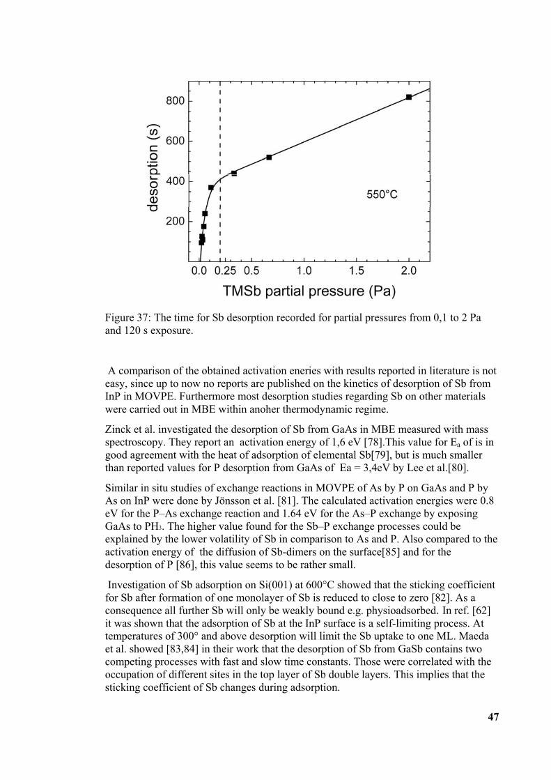
47
Figure 37: The time for Sb desorption recorded for partial pressures from 0,1 to 2 Paand 120 s exposure.
A comparison of the obtained activation eneries with results reported in literature is noteasy, since up to now no reports are published on the kinetics of desorption of Sb fromInP in MOVPE. Furthermore most desorption studies regarding Sb on other materialswere carried out in MBE within anoher thermodynamic regime.
Zinck et al. investigated the desorption of Sb from GaAs in MBE measured with massspectroscopy. They report an activation energy of 1,6 eV [78].This value for Ea of is ingood agreement with the heat of adsorption of elemental Sb[79], but is much smallerthan reported values for P desorption from GaAs of Ea = 3,4eV by Lee et al.[80].
Similar in situ studies of exchange reactions in MOVPE of As by P on GaAs and P byAs on InP were done by Jönsson et al. [81]. The calculated activation energies were 0.8eV for the P–As exchange reaction and 1.64 eV for the As–P exchange by exposingGaAs to PH3. The higher value found for the Sb–P exchange processes could beexplained by the lower volatility of Sb in comparison to As and P. Also compared to theactivation energy of the diffusion of Sb-dimers on the surface[85] and for thedesorption of P [86], this value seems to be rather small.
Investigation of Sb adsorption on Si(001) at 600°C showed that the sticking coefficientfor Sb after formation of one monolayer of Sb is reduced to close to zero [82]. As aconsequence all further Sb will only be weakly bound e.g. physioadsorbed. In ref. [62]it was shown that the adsorption of Sb at the InP surface is a self-limiting process. Attemperatures of 300° and above desorption will limit the Sb uptake to one ML. Maedaet al. showed [83,84] in their work that the desorption of Sb from GaSb contains twocompeting processes with fast and slow time constants. Those were correlated with theoccupation of different sites in the top layer of Sb double layers. This implies that thesticking coefficient of Sb changes during adsorption.

48
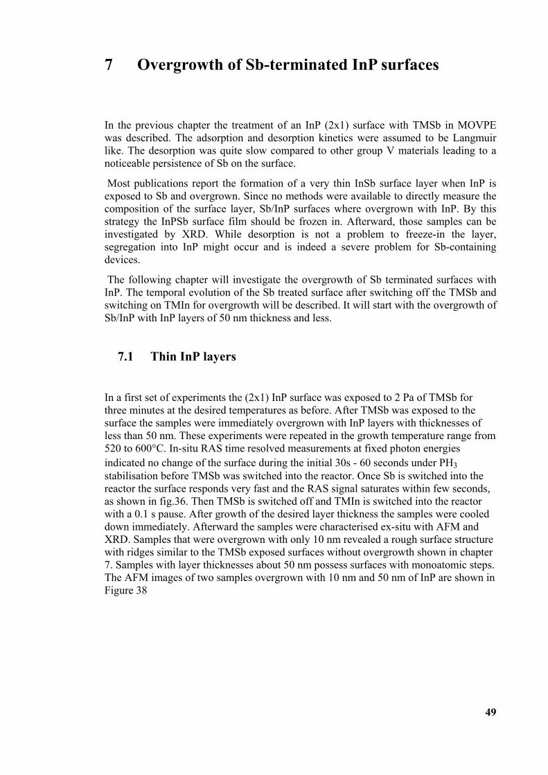
49
7 Overgrowth of Sb-terminated InP surfaces
In the previous chapter the treatment of an InP (2x1) surface with TMSb in MOVPEwas described. The adsorption and desorption kinetics were assumed to be Langmuirlike. The desorption was quite slow compared to other group V materials leading to anoticeable persistence of Sb on the surface.
Most publications report the formation of a very thin InSb surface layer when InP isexposed to Sb and overgrown. Since no methods were available to directly measure thecomposition of the surface layer, Sb/InP surfaces where overgrown with InP. By thisstrategy the InPSb surface film should be frozen in. Afterward, those samples can beinvestigated by XRD. While desorption is not a problem to freeze-in the layer,segregation into InP might occur and is indeed a severe problem for Sb-containingdevices.
The following chapter will investigate the overgrowth of Sb terminated surfaces withInP. The temporal evolution of the Sb treated surface after switching off the TMSb andswitching on TMIn for overgrowth will be described. It will start with the overgrowth ofSb/InP with InP layers of 50 nm thickness and less.
7.1 Thin InP layers
In a first set of experiments the (2x1) InP surface was exposed to 2 Pa of TMSb forthree minutes at the desired temperatures as before. After TMSb was exposed to thesurface the samples were immediately overgrown with InP layers with thicknesses ofless than 50 nm. These experiments were repeated in the growth temperature range from520 to 600°C. In-situ RAS time resolved measurements at fixed photon energiesindicated no change of the surface during the initial 30s - 60 seconds under PH3stabilisation before TMSb was switched into the reactor. Once Sb is switched into thereactor the surface responds very fast and the RAS signal saturates within few seconds,as shown in fig.36. Then TMSb is switched off and TMIn is switched into the reactorwith a 0.1 s pause. After growth of the desired layer thickness the samples were cooleddown immediately. Afterward the samples were characterised ex-situ with AFM andXRD. Samples that were overgrown with only 10 nm revealed a rough surface structurewith ridges similar to the TMSb exposed surfaces without overgrowth shown in chapter7. Samples with layer thicknesses about 50 nm possess surfaces with monoatomic steps.The AFM images of two samples overgrown with 10 nm and 50 nm of InP are shown inFigure 38
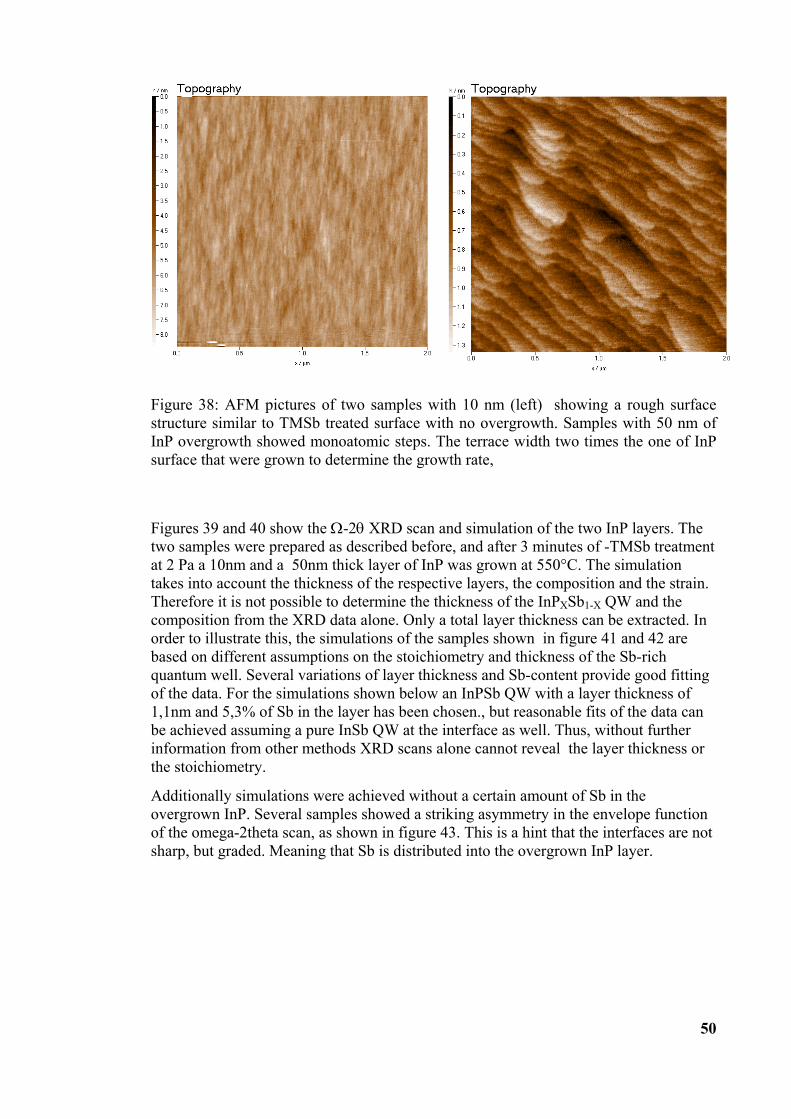
50
Figure 38: AFM pictures of two samples with 10 nm (left) showing a rough surfacestructure similar to TMSb treated surface with no overgrowth. Samples with 50 nm ofInP overgrowth showed monoatomic steps. The terrace width two times the one of InPsurface that were grown to determine the growth rate,
Figures 39 and 40 show the Ω-2θ XRD scan and simulation of the two InP layers. Thetwo samples were prepared as described before, and after 3 minutes of -TMSb treatmentat 2 Pa a 10nm and a 50nm thick layer of InP was grown at 550°C. The simulationtakes into account the thickness of the respective layers, the composition and the strain.Therefore it is not possible to determine the thickness of the InPXSb1-X QW and thecomposition from the XRD data alone. Only a total layer thickness can be extracted. Inorder to illustrate this, the simulations of the samples shown in figure 41 and 42 arebased on different assumptions on the stoichiometry and thickness of the Sb-richquantum well. Several variations of layer thickness and Sb-content provide good fittingof the data. For the simulations shown below an InPSb QW with a layer thickness of1,1nm and 5,3% of Sb in the layer has been chosen., but reasonable fits of the data canbe achieved assuming a pure InSb QW at the interface as well. Thus, without furtherinformation from other methods XRD scans alone cannot reveal the layer thickness orthe stoichiometry.
Additionally simulations were achieved without a certain amount of Sb in theovergrown InP. Several samples showed a striking asymmetry in the envelope functionof the omega-2theta scan, as shown in figure 43. This is a hint that the interfaces are notsharp, but graded. Meaning that Sb is distributed into the overgrown InP layer.
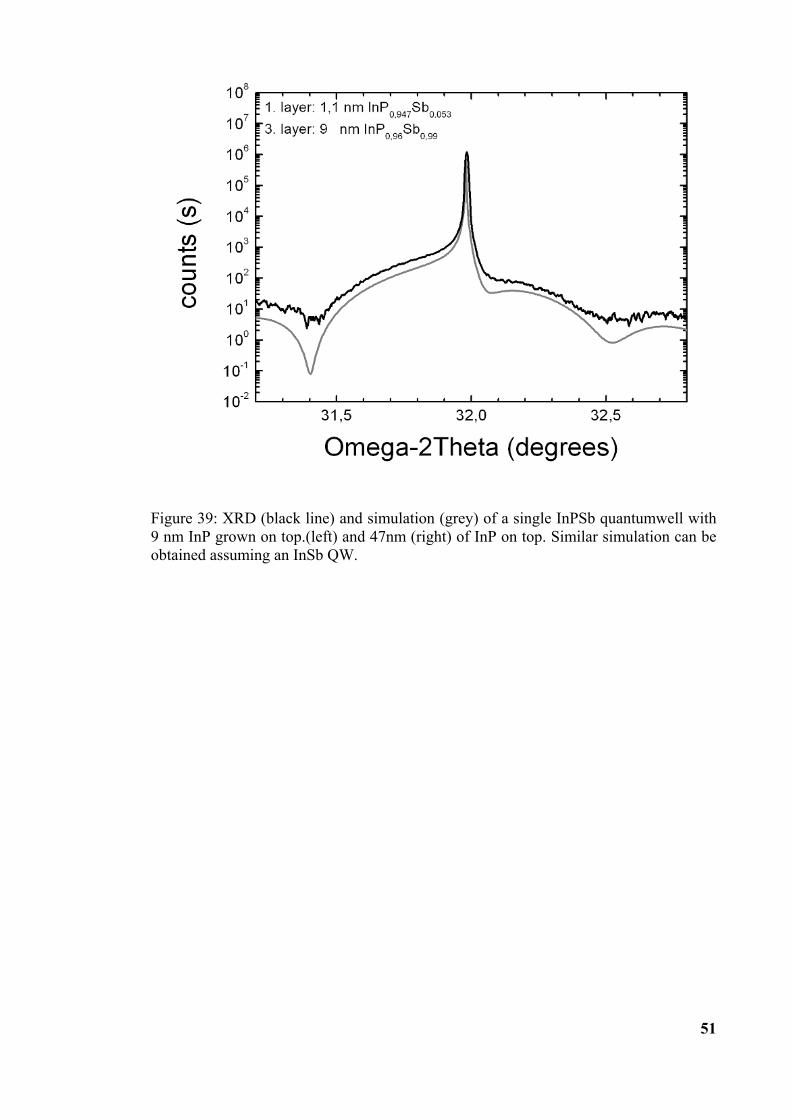
51
Figure 39: XRD (black line) and simulation (grey) of a single InPSb quantumwell with9 nm InP grown on top.(left) and 47nm (right) of InP on top. Similar simulation can beobtained assuming an InSb QW.
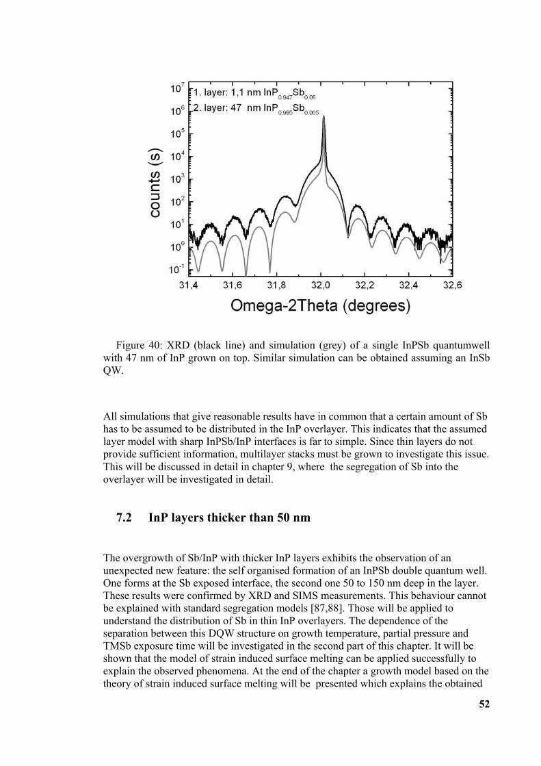
52
Figure 40: XRD (black line) and simulation (grey) of a single InPSb quantumwellwith 47 nm of InP grown on top. Similar simulation can be obtained assuming an InSbQW.
All simulations that give reasonable results have in common that a certain amount of Sbhas to be assumed to be distributed in the InP overlayer. This indicates that the assumedlayer model with sharp InPSb/InP interfaces is far to simple. Since thin layers do notprovide sufficient information, multilayer stacks must be grown to investigate this issue.This will be discussed in detail in chapter 9, where the segregation of Sb into theoverlayer will be investigated in detail.
7.2 InP layers thicker than 50 nm
The overgrowth of Sb/InP with thicker InP layers exhibits the observation of anunexpected new feature: the self organised formation of an InPSb double quantum well.One forms at the Sb exposed interface, the second one 50 to 150 nm deep in the layer.These results were confirmed by XRD and SIMS measurements. This behaviour cannotbe explained with standard segregation models [87,88]. Those will be applied tounderstand the distribution of Sb in thin InP overlayers. The dependence of theseparation between this DQW structure on growth temperature, partial pressure andTMSb exposure time will be investigated in the second part of this chapter. It will beshown that the model of strain induced surface melting can be applied successfully toexplain the observed phenomena. At the end of the chapter a growth model based on thetheory of strain induced surface melting will be presented which explains the obtained
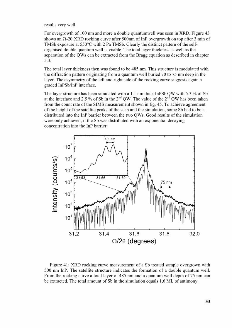
53
results very well.
For overgrowth of 100 nm and more a double quantumwell was seen in XRD. Figure 43shows an Ω-2θ XRD rocking curve after 500nm of InP overgrowth on top after 3 min ofTMSb exposure at 550°C with 2 Pa TMSb. Clearly the distinct pattern of the self-organised double quantum well is visible. The total layer thickness as well as theseparation of the QWs can be extracted from the Bragg equation as described in chapter5.3.
The total layer thickness then was found to be 485 nm. This structure is modulated withthe diffraction pattern originating from a quantum well buried 70 to 75 nm deep in thelayer. The asymmetry of the left and right side of the rocking curve suggests again agraded InPSb/InP interface.
The layer structure has been simulated with a 1.1 nm thick InPSb QW with 5.3 % of Sbat the interface and 2.5 % of Sb in the 2nd QW. The value of the 2nd QW has been takenfrom the count rate of the SIMS measurement shown in fig. 45. To achieve agreementof the height of the satellite peaks of the scan and the simulation, some Sb had to be adistributed into the InP barrier between the two QWs. Good results of the simulationwere only achieved, if the Sb was distributed with an exponential decayingconcentration into the InP barrier.
Figure 41: XRD rocking curve measurement of a Sb treated sample overgrown with500 nm InP. The satellite structure indicates the formation of a double quantum well.From the rocking curve a total layer of 485 nm and a quantum well depth of 75 nm canbe extracted. The total amount of Sb in the simulation equals 1,6 ML of antimony.
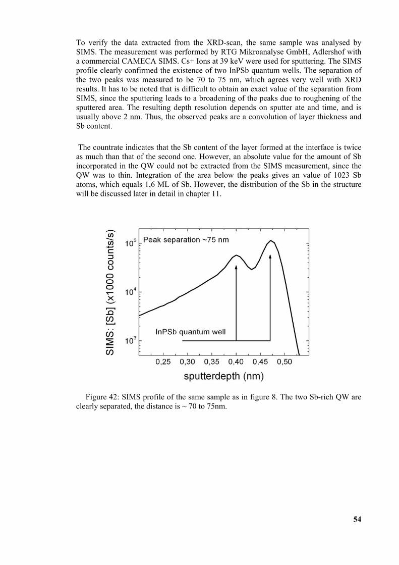
54
To verify the data extracted from the XRD-scan, the same sample was analysed bySIMS. The measurement was performed by RTG Mikroanalyse GmbH, Adlershof witha commercial CAMECA SIMS. Cs+ Ions at 39 keV were used for sputtering. The SIMSprofile clearly confirmed the existence of two InPSb quantum wells. The separation ofthe two peaks was measured to be 70 to 75 nm, which agrees very well with XRDresults. It has to be noted that is difficult to obtain an exact value of the separation fromSIMS, since the sputtering leads to a broadening of the peaks due to roughening of thesputtered area. The resulting depth resolution depends on sputter ate and time, and isusually above 2 nm. Thus, the observed peaks are a convolution of layer thickness andSb content.
The countrate indicates that the Sb content of the layer formed at the interface is twiceas much than that of the second one. However, an absolute value for the amount of Sbincorporated in the QW could not be extracted from the SIMS measurement, since theQW was to thin. Integration of the area below the peaks gives an value of 1023 Sbatoms, which equals 1,6 ML of Sb. However, the distribution of the Sb in the structurewill be discussed later in detail in chapter 11.
Figure 42: SIMS profile of the same sample as in figure 8. The two Sb-rich QW areclearly separated, the distance is ~ 70 to 75nm.
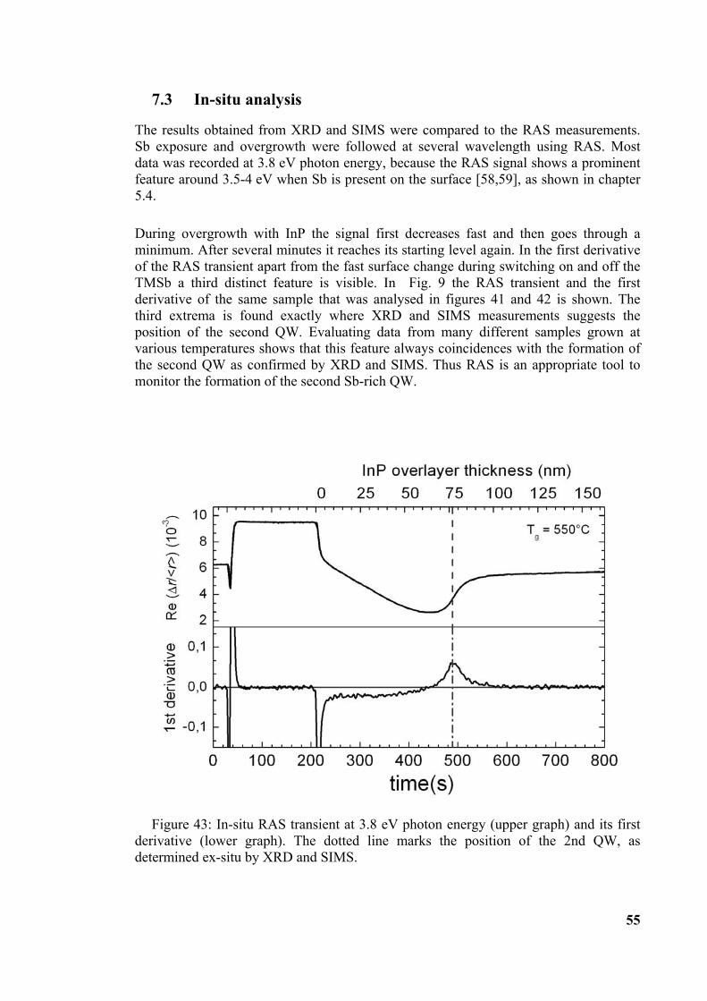
55
7.3 In-situ analysis
The results obtained from XRD and SIMS were compared to the RAS measurements.Sb exposure and overgrowth were followed at several wavelength using RAS. Mostdata was recorded at 3.8 eV photon energy, because the RAS signal shows a prominentfeature around 3.5-4 eV when Sb is present on the surface [58,59], as shown in chapter5.4.
During overgrowth with InP the signal first decreases fast and then goes through aminimum. After several minutes it reaches its starting level again. In the first derivativeof the RAS transient apart from the fast surface change during switching on and off theTMSb a third distinct feature is visible. In Fig. 9 the RAS transient and the firstderivative of the same sample that was analysed in figures 41 and 42 is shown. Thethird extrema is found exactly where XRD and SIMS measurements suggests theposition of the second QW. Evaluating data from many different samples grown atvarious temperatures shows that this feature always coincidences with the formation ofthe second QW as confirmed by XRD and SIMS. Thus RAS is an appropriate tool tomonitor the formation of the second Sb-rich QW.
Figure 43: In-situ RAS transient at 3.8 eV photon energy (upper graph) and its firstderivative (lower graph). The dotted line marks the position of the 2nd QW, asdetermined ex-situ by XRD and SIMS.
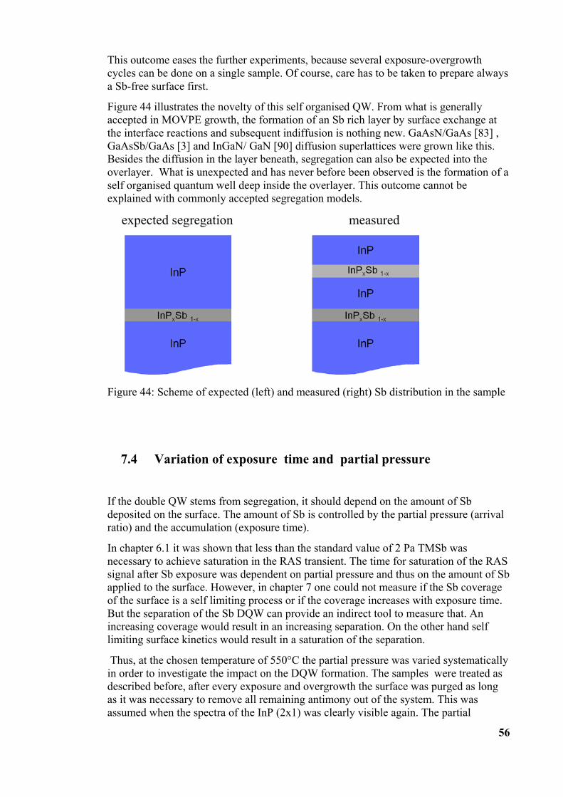
56
This outcome eases the further experiments, because several exposure-overgrowthcycles can be done on a single sample. Of course, care has to be taken to prepare alwaysa Sb-free surface first.
Figure 44 illustrates the novelty of this self organised QW. From what is generallyaccepted in MOVPE growth, the formation of an Sb rich layer by surface exchange atthe interface reactions and subsequent indiffusion is nothing new. GaAsN/GaAs [83] ,GaAsSb/GaAs [3] and InGaN/ GaN [90] diffusion superlattices were grown like this.Besides the diffusion in the layer beneath, segregation can also be expected into theoverlayer. What is unexpected and has never before been observed is the formation of aself organised quantum well deep inside the overlayer. This outcome cannot beexplained with commonly accepted segregation models.
expected segregation measured
Figure 44: Scheme of expected (left) and measured (right) Sb distribution in the sample
7.4 Variation of exposure time and partial pressure
If the double QW stems from segregation, it should depend on the amount of Sbdeposited on the surface. The amount of Sb is controlled by the partial pressure (arrivalratio) and the accumulation (exposure time).
In chapter 6.1 it was shown that less than the standard value of 2 Pa TMSb wasnecessary to achieve saturation in the RAS transient. The time for saturation of the RASsignal after Sb exposure was dependent on partial pressure and thus on the amount of Sbapplied to the surface. However, in chapter 7 one could not measure if the Sb coverageof the surface is a self limiting process or if the coverage increases with exposure time.But the separation of the Sb DQW can provide an indirect tool to measure that. Anincreasing coverage would result in an increasing separation. On the other hand selflimiting surface kinetics would result in a saturation of the separation.
Thus, at the chosen temperature of 550°C the partial pressure was varied systematicallyin order to investigate the impact on the DQW formation. The samples were treated asdescribed before, after every exposure and overgrowth the surface was purged as longas it was necessary to remove all remaining antimony out of the system. This wasassumed when the spectra of the InP (2x1) was clearly visible again. The partial
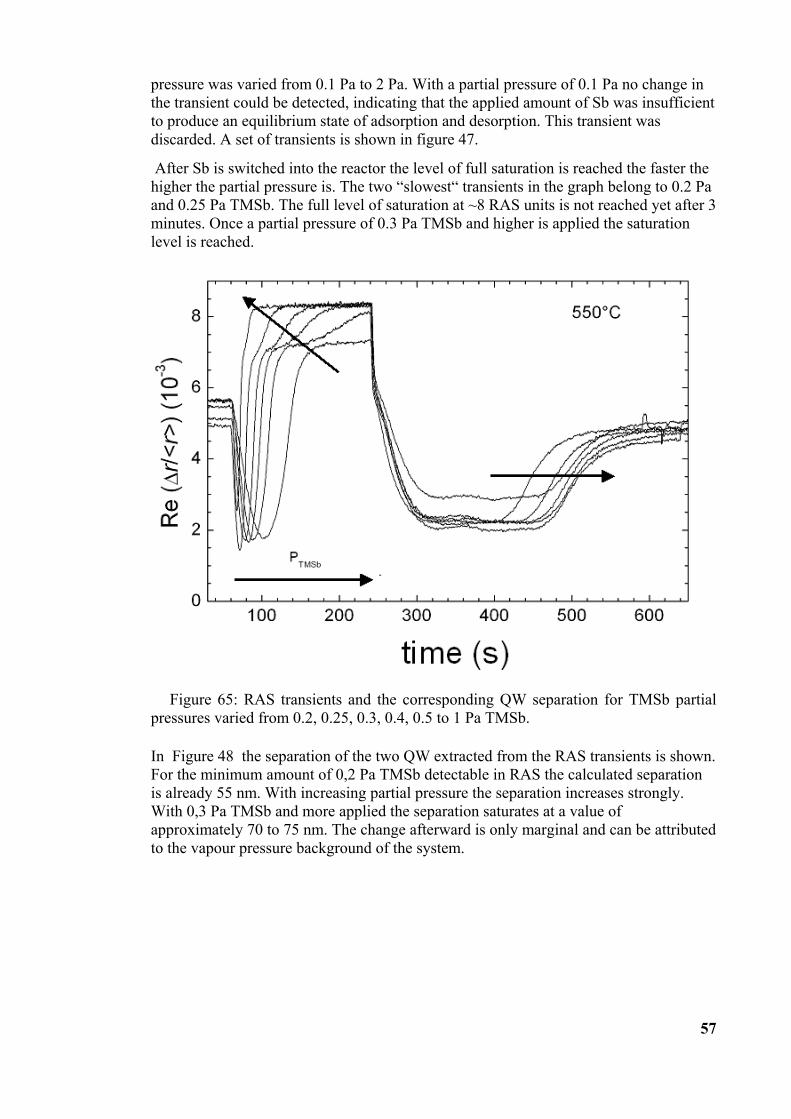
57
pressure was varied from 0.1 Pa to 2 Pa. With a partial pressure of 0.1 Pa no change inthe transient could be detected, indicating that the applied amount of Sb was insufficientto produce an equilibrium state of adsorption and desorption. This transient wasdiscarded. A set of transients is shown in figure 47.
After Sb is switched into the reactor the level of full saturation is reached the faster thehigher the partial pressure is. The two “slowest“ transients in the graph belong to 0.2 Paand 0.25 Pa TMSb. The full level of saturation at ~8 RAS units is not reached yet after 3minutes. Once a partial pressure of 0.3 Pa TMSb and higher is applied the saturationlevel is reached.
Figure 65: RAS transients and the corresponding QW separation for TMSb partialpressures varied from 0.2, 0.25, 0.3, 0.4, 0.5 to 1 Pa TMSb.
In Figure 48 the separation of the two QW extracted from the RAS transients is shown.For the minimum amount of 0,2 Pa TMSb detectable in RAS the calculated separationis already 55 nm. With increasing partial pressure the separation increases strongly.With 0,3 Pa TMSb and more applied the separation saturates at a value ofapproximately 70 to 75 nm. The change afterward is only marginal and can be attributedto the vapour pressure background of the system.
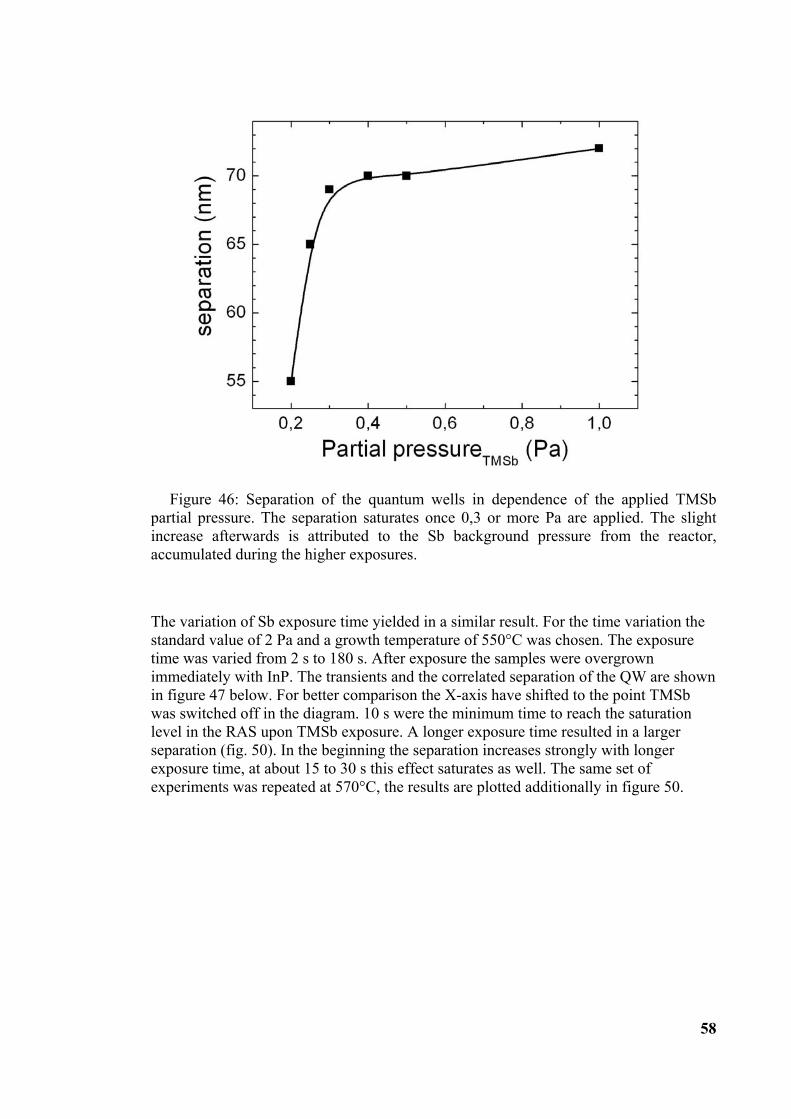
58
Figure 46: Separation of the quantum wells in dependence of the applied TMSbpartial pressure. The separation saturates once 0,3 or more Pa are applied. The slightincrease afterwards is attributed to the Sb background pressure from the reactor,accumulated during the higher exposures.
The variation of Sb exposure time yielded in a similar result. For the time variation thestandard value of 2 Pa and a growth temperature of 550°C was chosen. The exposuretime was varied from 2 s to 180 s. After exposure the samples were overgrownimmediately with InP. The transients and the correlated separation of the QW are shownin figure 47 below. For better comparison the X-axis have shifted to the point TMSbwas switched off in the diagram. 10 s were the minimum time to reach the saturationlevel in the RAS upon TMSb exposure. A longer exposure time resulted in a largerseparation (fig. 50). In the beginning the separation increases strongly with longerexposure time, at about 15 to 30 s this effect saturates as well. The same set ofexperiments was repeated at 570°C, the results are plotted additionally in figure 50.
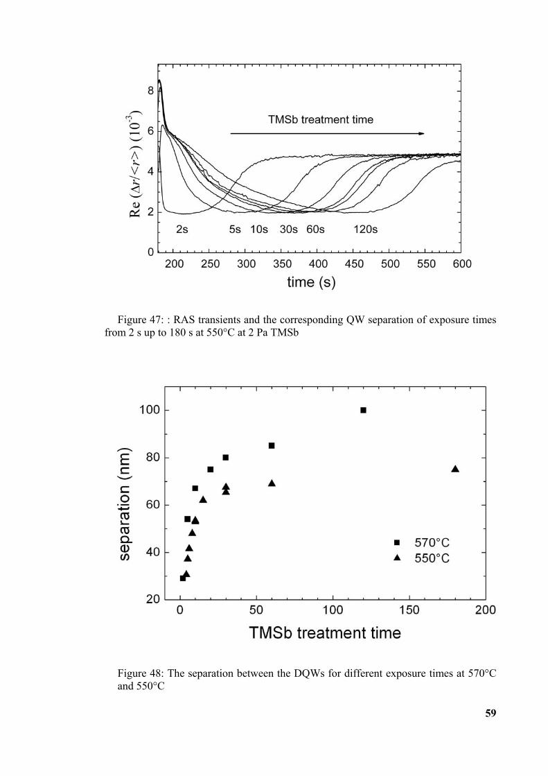
59
Figure 47: : RAS transients and the corresponding QW separation of exposure timesfrom 2 s up to 180 s at 550°C at 2 Pa TMSb
Figure 48: The separation between the DQWs for different exposure times at 570°Cand 550°C
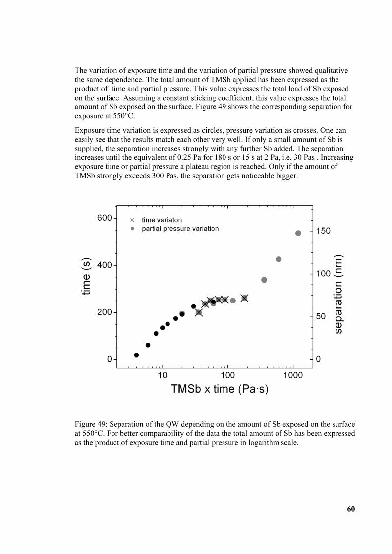
60
The variation of exposure time and the variation of partial pressure showed qualitativethe same dependence. The total amount of TMSb applied has been expressed as theproduct of time and partial pressure. This value expresses the total load of Sb exposedon the surface. Assuming a constant sticking coefficient, this value expresses the totalamount of Sb exposed on the surface. Figure 49 shows the corresponding separation forexposure at 550°C.
Exposure time variation is expressed as circles, pressure variation as crosses. One caneasily see that the results match each other very well. If only a small amount of Sb issupplied, the separation increases strongly with any further Sb added. The separationincreases until the equivalent of 0.25 Pa for 180 s or 15 s at 2 Pa, i.e. 30 Pas . Increasingexposure time or partial pressure a plateau region is reached. Only if the amount ofTMSb strongly exceeds 300 Pas, the separation gets noticeable bigger.
Figure 49: Separation of the QW depending on the amount of Sb exposed on the surfaceat 550°C. For better comparability of the data the total amount of Sb has been expressedas the product of exposure time and partial pressure in logarithm scale.
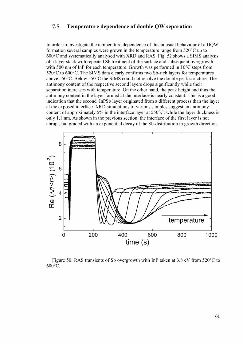
61
7.5 Temperature dependence of double QW separation
In order to investigate the temperature dependence of this unusual behaviour of a DQWformation several samples were grown in the temperature range from 520°C up to600°C and systematically analysed with XRD and RAS. Fig. 52 shows a SIMS analysisof a layer stack with repeated Sb treatment of the surface and subsequent overgrowthwith 500 nm of InP for each temperature. Growth was performed in 10°C steps from520°C to 600°C. The SIMS data clearly confirms two Sb-rich layers for temperaturesabove 550°C. Below 550°C the SIMS could not resolve the double peak structure. Theantimony content of the respective second layers drops significantly while theirseparation increases with temperature. On the other hand, the peak height and thus theantimony content in the layer formed at the interface is nearly constant. This is a goodindication that the second InPSb layer originated from a different process than the layerat the exposed interface. XRD simulations of various samples suggest an antimonycontent of approximately 5% in the interface layer at 550°C, while the layer thickness isonly 1,1 nm. As shown in the previous section, the interface of the first layer is notabrupt, but graded with an exponential decay of the Sb-distribution in growth direction.
Figure 50: RAS transients of Sb overgrowth with InP taken at 3.8 eV from 520°C to600°C.
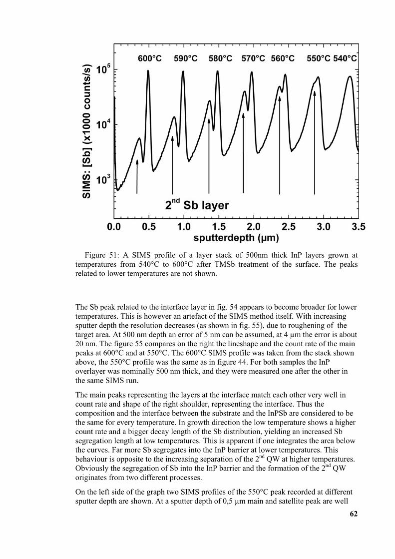
62
Figure 51: A SIMS profile of a layer stack of 500nm thick InP layers grown attemperatures from 540°C to 600°C after TMSb treatment of the surface. The peaksrelated to lower temperatures are not shown.
The Sb peak related to the interface layer in fig. 54 appears to become broader for lowertemperatures. This is however an artefact of the SIMS method itself. With increasingsputter depth the resolution decreases (as shown in fig. 55), due to roughening of thetarget area. At 500 nm depth an error of 5 nm can be assumed, at 4 µm the error is about20 nm. The figure 55 compares on the right the lineshape and the count rate of the mainpeaks at 600°C and at 550°C. The 600°C SIMS profile was taken from the stack shownabove, the 550°C profile was the same as in figure 44. For both samples the InPoverlayer was nominally 500 nm thick, and they were measured one after the other inthe same SIMS run.
The main peaks representing the layers at the interface match each other very well incount rate and shape of the right shoulder, representing the interface. Thus thecomposition and the interface between the substrate and the InPSb are considered to bethe same for every temperature. In growth direction the low temperature shows a highercount rate and a bigger decay length of the Sb distribution, yielding an increased Sbsegregation length at low temperatures. This is apparent if one integrates the area belowthe curves. Far more Sb segregates into the InP barrier at lower temperatures. Thisbehaviour is opposite to the increasing separation of the 2nd QW at higher temperatures.Obviously the segregation of Sb into the InP barrier and the formation of the 2nd QWoriginates from two different processes.
On the left side of the graph two SIMS profiles of the 550°C peak recorded at differentsputter depth are shown. At a sputter depth of 0,5 µm main and satellite peak are well
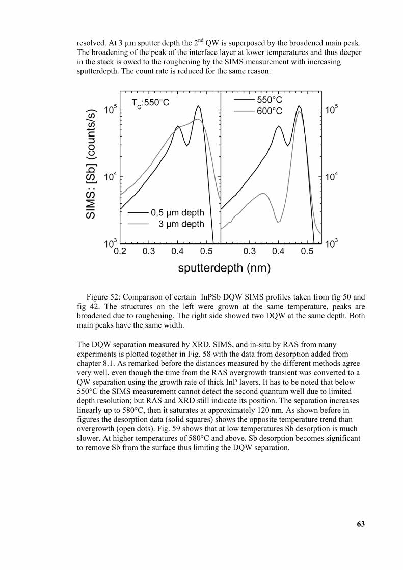
63
resolved. At 3 µm sputter depth the 2nd QW is superposed by the broadened main peak.The broadening of the peak of the interface layer at lower temperatures and thus deeperin the stack is owed to the roughening by the SIMS measurement with increasingsputterdepth. The count rate is reduced for the same reason.
Figure 52: Comparison of certain InPSb DQW SIMS profiles taken from fig 50 andfig 42. The structures on the left were grown at the same temperature, peaks arebroadened due to roughening. The right side showed two DQW at the same depth. Bothmain peaks have the same width.
The DQW separation measured by XRD, SIMS, and in-situ by RAS from manyexperiments is plotted together in Fig. 58 with the data from desorption added fromchapter 8.1. As remarked before the distances measured by the different methods agreevery well, even though the time from the RAS overgrowth transient was converted to aQW separation using the growth rate of thick InP layers. It has to be noted that below550°C the SIMS measurement cannot detect the second quantum well due to limiteddepth resolution; but RAS and XRD still indicate its position. The separation increaseslinearly up to 580°C, then it saturates at approximately 120 nm. As shown before infigures the desorption data (solid squares) shows the opposite temperature trend thanovergrowth (open dots). Fig. 59 shows that at low temperatures Sb desorption is muchslower. At higher temperatures of 580°C and above. Sb desorption becomes significantto remove Sb from the surface thus limiting the DQW separation.
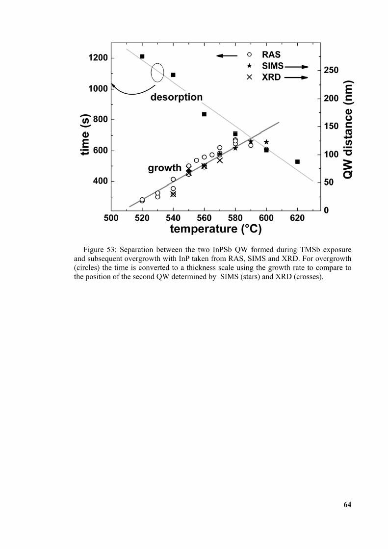
64
Figure 53: Separation between the two InPSb QW formed during TMSb exposureand subsequent overgrowth with InP taken from RAS, SIMS and XRD. For overgrowth(circles) the time is converted to a thickness scale using the growth rate to compare tothe position of the second QW determined by SIMS (stars) and XRD (crosses).
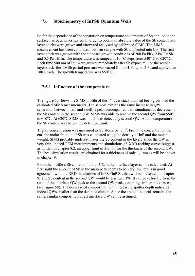
65
7.6 Stoichiometry of InPSb Quantum Wells
So far the dependence of the separation on temperature and amount of Sb applied to thesurface has been investigated. In order to obtain an absolute value of the Sb content twolayer stacks were grown and afterward analysed by calibrated SIMS. The SIMSmeasurement has been calibrated with an sample with Sb implanted into InP. The firstlayer stack was grown with the standard growth conditions of 200 Pa Ph3, 2 Pa TMSband 0,5 Pa TMIn. The temperature was ramped in 10° C steps from 540° C to 620° C.Each time 500 nm of InP were grown immediately after Sb exposure. For the secondlayer stack the TMSb partial pressure was varied from 0,1 Pa up to 2 Pa and applied for180 s each. The growth temperature was 550° C.
7.6.1 Influence of the temperature
The figure 57 shows the SIMS profile of the 1st layer stack that had been grown for thecalibrated SIMS measurements. The sample exhibits the same increase in QWseparation between main and satellite peak accompanied with simultaneous decrease ofthe Sb content in the second QW. SIMS was able to resolve the second QW from 550°Cto 610°C. At 620°C SIMS was not able to detect any second QW. At this temperaturethe Sb content was below the detection limit.
The Sb concentration was measured as Sb atoms per cm3. From the concentration percm3 the molar fraction of Sb was calculated using the density of InP and the molarweight. SIMS probably underestimates the Sb content in the layer, since the QW isvery thin. Indeed TEM measurements and simulations of XRD rocking curves suggest,as written in chapter 8.2, an upper limit of 2-3 nm for the thickness of the second QW.The best simulation results are obtained for a thickness of only 1,1 nm as will be shownin chapter 9.
From the profile a Sb content of about 3 % in the interface layer can be calculated. Atfirst sight the amount of Sb in the main peak seems to be very low, but is in goodagreement with the XRD simulations of InPSb/InP SL that will be presented in chapter9. The Sb content in the second QW would be less than 1%. It can be extracted from theratio of the interface QW peak to the second QW peak, assuming similar thicknesses(see figure 58). The decrease of composition with increasing sputter depth indicatesindeed QWs smaller than the depth resolution. Since the area of the peak remains thesame, similar composition of all interface QW can be assumed.
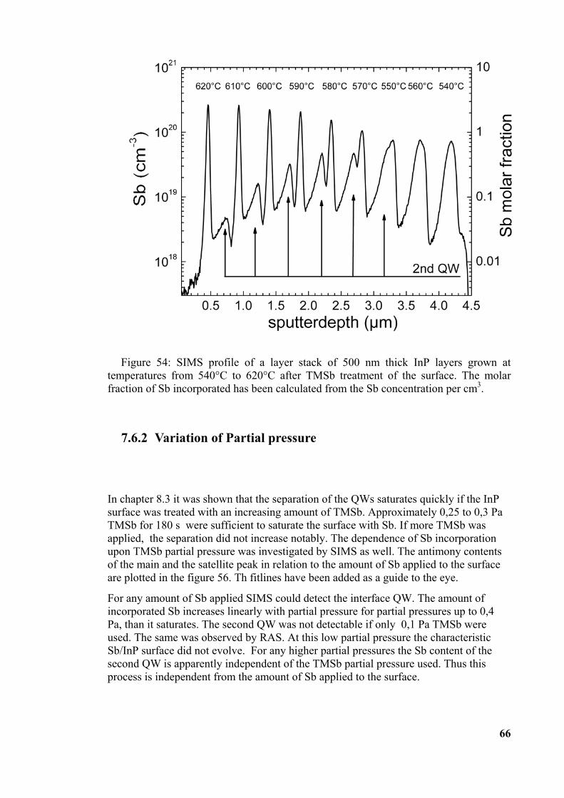
66
Figure 54: SIMS profile of a layer stack of 500 nm thick InP layers grown attemperatures from 540°C to 620°C after TMSb treatment of the surface. The molarfraction of Sb incorporated has been calculated from the Sb concentration per cm3.
7.6.2 Variation of Partial pressure
In chapter 8.3 it was shown that the separation of the QWs saturates quickly if the InPsurface was treated with an increasing amount of TMSb. Approximately 0,25 to 0,3 PaTMSb for 180 s were sufficient to saturate the surface with Sb. If more TMSb wasapplied, the separation did not increase notably. The dependence of Sb incorporationupon TMSb partial pressure was investigated by SIMS as well. The antimony contentsof the main and the satellite peak in relation to the amount of Sb applied to the surfaceare plotted in the figure 56. Th fitlines have been added as a guide to the eye.
For any amount of Sb applied SIMS could detect the interface QW. The amount ofincorporated Sb increases linearly with partial pressure for partial pressures up to 0,4Pa, than it saturates. The second QW was not detectable if only 0,1 Pa TMSb wereused. The same was observed by RAS. At this low partial pressure the characteristicSb/InP surface did not evolve. For any higher partial pressures the Sb content of thesecond QW is apparently independent of the TMSb partial pressure used. Thus thisprocess is independent from the amount of Sb applied to the surface.
67
Figure 55: Sb fraction incorporated in interface QW and the 2nd QW resulting fromexposure with various Sb partial pressures. The corresponding separation is plotted inthe figure below. The Sb ratio does not increase after an minimum exposure of 0,3 Pafor 180 s.
From the presented experiments it can be concluded that ~0,3 Pa or 15 s of TMSbtreatment are sufficient to fully saturate the InP surface with Sb. Applying additional Sbdoes not increase the surface coverage. These findings can be used to estimate the actualamount of Sb deposited on the surface using the growth rate of GaAsSb. At 550°C ~ 1µm GaAsSb has been grown with 0,8 Pa TEGa and 1 Pa TMSb. Assuming the growthrate of GaAsSb a maximum amount of equivalent 3,5 MLs of Sb have been depositedon the surface during 15 s of TMSb treatment or of exposure with 0, 25 Pa TMSb for180 s.
This value of 3,5 MLs is rather high compared to the amount of Sb incorporated into theQWs as measured by SIMS. From SIMS the Sb content in InpSb was 5 % at theinterface QW and less than half of that in the second QW. XRD measurements andsimulations proposed a layer thickness of 2 nm. Thus only 0,3 ML of Sb areincorporated in these two layers. This is less than 10 % of the initially deposited Sb.
Since desorption of Sb at 550°C is very slow compared to overgrowth, a loss into thevapour phase can be excluded as well. The questions remaining is where all the Sb hasgone. The only remaining possibility is the InP barrier layer. Rocking curves of thinInP layers gave reason to assume graded InPSb/InP interfaces with a certain amount ofSb distributed into the InP overlayer. Therefore in the following chapter the distributionof Sb into the InP barrier will be investigated.
Another possibility would be a change of the sticking coefficient as suggested in figure

68
46. The amount of Sb deposited at which at the slope changes indicates the formation ofa Sb saturated surface layer. Until this point the sticking coefficient is very high, and theratio of incoming flux and deposited Sb is close to unity. After this point in time thesurface is fully covered with antimony, and the sticking coefficient becomes close tozero, as suggested by [82]. Further Sb applied will not stay on the surface.
69
8 Segregation of Sb in InPSb/InP superlattices
In the previous chapters the growth mechanism leading to the formation of the selforganised double QW structure has been investigated. The experiments supplied a goodunderstanding of the observed phenomena. A quantitative estimate of the Sb applied tothe surface differed by an order of magnitude from the measured Sb incorporation intothe QW by SIMS. A variation of either treatment time or applied partial pressureresulted in a similar separation of the two quantum wells. Once a critical amount of 0,3Pa for 180 s or 2 Pa for ~15 s is applied, the separation does not increase anymore. Thusa comparison of these parameters with the growth rate of GsAsSb delivered an estimateof the amount of Sb necessary to achieve full saturation with Sb of the Sb/InP surface.The obtained value of approximately 3,5 deposited monolayers of Sb differs drasticallyfrom the 0,37 ML Sb that are incorporated into the two InPSb layers, as obtained bySIMS and XRD rocking curve simulations.
The remaining question is whether the previous assumption on the amount of Sbdeposited on the surface is wrong or if the Sb is incorporated elsewhere. Desorption ofSb can be neglected at the chosen growth temperature of 550°C. Sb is reported tosegregates strongly at heterointerfaces [3,4,67]. Therefore the missing antimony isassumed to be incorporated into the InP overlayer. In order to investigate thesegregation of Sb into InP a set of strained InP/InPSb superlattices was grown.
8.1 Models for segregation
Segregation is a well known effect in III-V ternary alloys, but is mostly attributed togroup III elements, describing the exchange between bulk and surface layers.Principally segregation means the enrichment of an element at the surface with respectto the bulk composition. There is a long history of such models in literature, describingsegregation in metal alloys. A good summary is given by Moison et al. [91] and Weaveret al. [92].
During growth of an alloy one species preferably populates the surface. Sb ↔Pexchange leads to the formation of an Sb containing layer, serving as substrate, which isimmediately overgrown. The segregating amount of Sb decreases with each layer. Forthe segregation description Muraki et al.[88] assumed that a certain fraction σ of atomson the top surface layer segregates to the next layer at every monolayer grown. Thusσ denoted the segregation probability. The remaining quantity (1-σ ) of atoms areincorporated into the bulk before the next monolayer is completed. Segregationcoefficients from 0.45 (370°C) to 0,8 (520°C) were found for In in InGaAs/GaAs – QWusing SIMS and PL.
A more quantitative model was proposed by Muriaki [81]. In his model aphenomenological description of the segregation of In in InGaAs/GaAs QW was givenbased on experimental data obtained with SIMS and PL. Muraki et al. found asignificant increase of the In segregation with increasing temperature and withdecreasing As pressure.
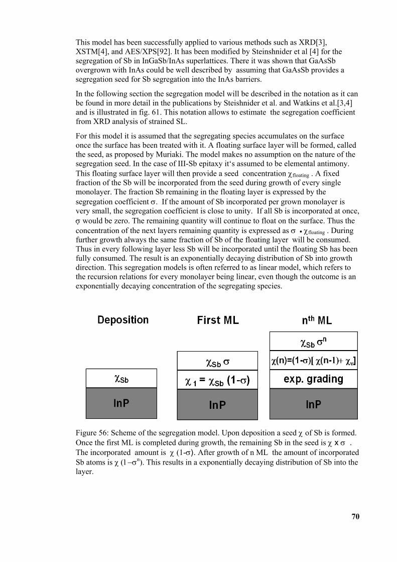
70
This model has been successfully applied to various methods such as XRD[3],XSTM[4], and AES/XPS[92]. It has been modified by Steinshnider et al [4] for thesegregation of Sb in InGaSb/InAs superlattices. There it was shown that GaAsSbovergrown with InAs could be well described by assuming that GaAsSb provides asegregation seed for Sb segregation into the InAs barriers.
In the following section the segregation model will be described in the notation as it canbe found in more detail in the publications by Steishnider et al. and Watkins et al.[3,4]and is illustrated in fig. 61. This notation allows to estimate the segregation coefficientfrom XRD analysis of strained SL.
For this model it is assumed that the segregating species accumulates on the surfaceonce the surface has been treated with it. A floating surface layer will be formed, calledthe seed, as proposed by Muriaki. The model makes no assumption on the nature of thesegregation seed. In the case of III-Sb epitaxy it‘s assumed to be elemental antimony.This floating surface layer will then provide a seed concentration χfloating . A fixedfraction of the Sb will be incorporated from the seed during growth of every singlemonolayer. The fraction Sb remaining in the floating layer is expressed by thesegregation coefficient σ. If the amount of Sb incorporated per grown monolayer isvery small, the segregation coefficient is close to unity. If all Sb is incorporated at once,σ would be zero. The remaining quantity will continue to float on the surface. Thus theconcentration of the next layers remaining quantity is expressed as σ • χfloating . Duringfurther growth always the same fraction of Sb of the floating layer will be consumed.Thus in every following layer less Sb will be incorporated until the floating Sb has beenfully consumed. The result is an exponentially decaying distribution of Sb into growthdirection. This segregation models is often referred to as linear model, which refers tothe recursion relations for every monolayer being linear, even though the outcome is anexponentially decaying concentration of the segregating species.
Figure 56: Scheme of the segregation model. Upon deposition a seed χ of Sb is formed.Once the first ML is completed during growth, the remaining Sb in the seed is χ x σ .The incorporated amount is χ (1-σ). After growth of n ML the amount of incorporatedSb atoms is χ (1−σn). This results in a exponentially decaying distribution of Sb into thelayer.
71
The segregation profile is defined through the linear recursion relations describing theamount of Sb in the seed after growth of the nth ML and the fraction of Sb incorporatedin the nth ML:
)]1([)( −= nn floatingfloating χσχ , seed after growth of n ML
)]1()[1()( −−= nn floatingχσχ , Sb content in nth ML
with the starting condition ifloating x=)0(χ , with n being an integer number, labellingthe buried monolayer and χ(n) the incorporated fraction of Sb. In Sb epitaxy it there isusually an unwanted vapour pressure background from material deposited in the reactorduring exposure. After Sb is switched off, some of it will be activated and reach thesample as well. Thus, one must also take the contribution from this process intoaccount. Therefore a constant source term for the vapour background χν must be added,and the above recursion relations become inhomogeneous:
])1([)( vfloatingfloating nn χχσχ +−= , (8.1)
])1()[1()( vfloating nn χχσχ +−−= ,
With these relations one can describe the amount of Sb incorporated in the nth
monolayer. Combining the solutions of these two sets of recursion relations yields forthe final Sb-segregation profile:
)1()1()()( 10
nv
nin σχσσχχχ −+−−= − (8.2)
The first term represents an exponential decay of the Sb content in each successivelayers. If desorption is neglected, its total sum equals the initially deposited amount ofSb iχ . The second term accounts for the vapour background pressure 0χ from thereactor due to reevapouration of antimony. The mole fraction of antimony in the nth
monolayer is then given by
])1()[1()( vnn χχσχ +−−= (8.3)
The total amount of incorporated Sb in the whole barrier is then the sum over allmonolayers that have been grown. If desorption is neglected, it represents the totalsurface coverage after deposition as well.
72
∑+=N
T n1
0 )(χχχ (8.4)
This equation is of special interest for further analysis. In the previous chapters anestimation of the amount of Sb deposited on the surface has been made using theGaAsSb growth rate and the variation of treatment time of InP with TMSb. With thelast equation the amount of Sb deposited is directly accessible by XRD. This is veryhandy, since especially for diffusion SL that will be discussed in the followingparagraph, the thickness of the InPSb layer is not exactly known. One can extract thetotal amount of Sb from the location of the zeroth order satellite peak of a superlatticestructure without assuming a certain layer model. If segregation takes place asdescribed by this model, the amount of Sb incorporated will decline exponentially fromML to ML until the seed is fully consumed. The amount of Sb incorporated from theseed layer into the barrier should increase with barrier thickness and saturate. A plot ofχT versus grown ML then allows to determine the segregation coefficient σ and theamount of initially deposited Sb on the surface xin.
The origin of Sb segregation is attributed to different effects: The flux of incomingmaterial (In + P) is different to the substrate (InPSb). The mechanisms leading tosegregation are considered to be fast with respect to growth. Further Sb is considered tosegregate due to is large atomic size compared to P, thus this rather large atom isrepelled from the growing surface due to strain minimising the surface energy. The bulkbonding energies (EInP> EInSb) and the chemical reactivity (P > Sb) have been putforward as an origin of segregation as well, thus Sb has to segregate much stronger thanP. On the other hand studies of segregation of metals in III/V semiconductors haveshown that this arguments of „chemical trends“ is often contradicted [91].
In III-V heterostructure growth Sb segregation means that the InP/InPSb interfaceshould be more atomically abrupt than the InPSb/InP interface. The asymmetry of thesatellite peaks of the SL in fig. 63 indicate indeed to a compositional grading in growthdirection at the barriers.
8.2 XRD of indiffused InPSb/InP - Superlattices
In order to improve the quality of the predictions made on the actual layer model, theantimony-content of the quantum well and the antimony distribution throughout the InPoverlayer, a set of strained superlattices was grown. This reduces the degrees offreedom within the simulation parameters. The following sequence was repeated 10times for every superlattice: The InP surface was treated with 2 Pa of TMSb to form anInPSb film by P↔Sb exchange. Afterwards nominally 5, 10, 20, 30, 40 , 50 and 60 nmof InP were grown as a barrier layer with 200 Pa PH3 and 0,5 Pa TMIn. Then thesample was purged for 30 s with PH3 to remove excess antimony from the surface andsuppress Sb accumulation on the surface. For the first superlattice, a treatment time of
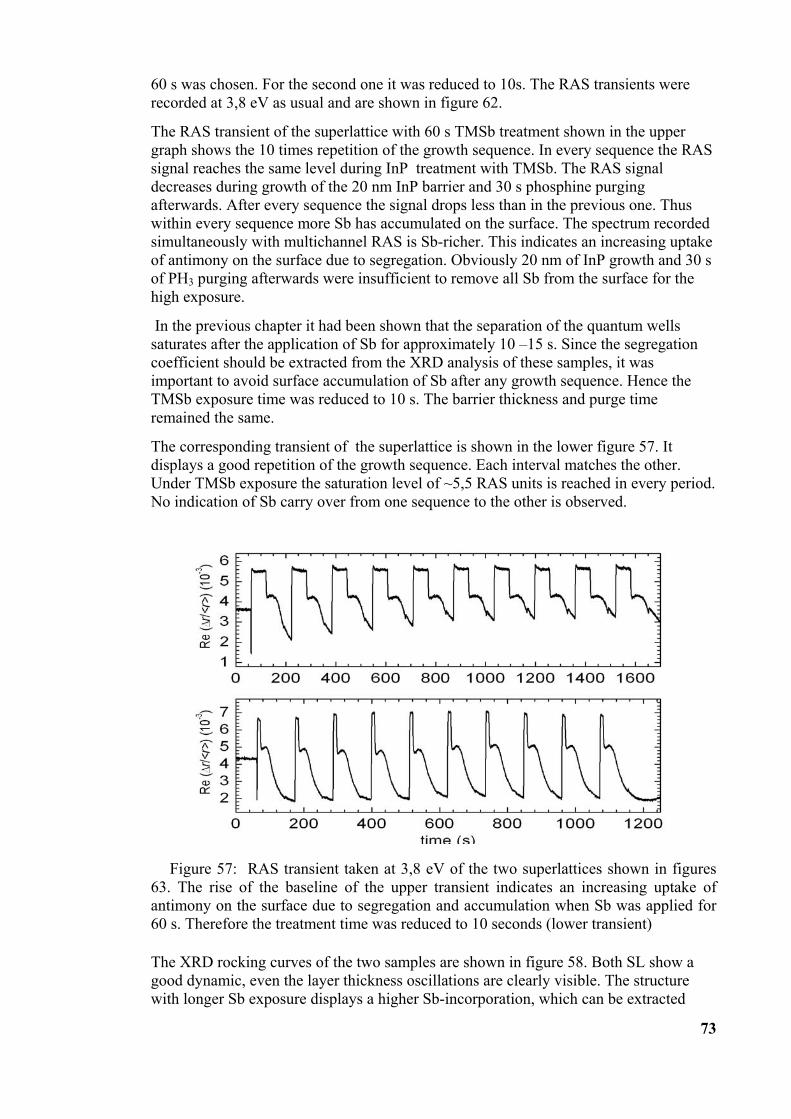
73
60 s was chosen. For the second one it was reduced to 10s. The RAS transients wererecorded at 3,8 eV as usual and are shown in figure 62.
The RAS transient of the superlattice with 60 s TMSb treatment shown in the uppergraph shows the 10 times repetition of the growth sequence. In every sequence the RASsignal reaches the same level during InP treatment with TMSb. The RAS signaldecreases during growth of the 20 nm InP barrier and 30 s phosphine purgingafterwards. After every sequence the signal drops less than in the previous one. Thuswithin every sequence more Sb has accumulated on the surface. The spectrum recordedsimultaneously with multichannel RAS is Sb-richer. This indicates an increasing uptakeof antimony on the surface due to segregation. Obviously 20 nm of InP growth and 30 sof PH3 purging afterwards were insufficient to remove all Sb from the surface for thehigh exposure.
In the previous chapter it had been shown that the separation of the quantum wellssaturates after the application of Sb for approximately 10 –15 s. Since the segregationcoefficient should be extracted from the XRD analysis of these samples, it wasimportant to avoid surface accumulation of Sb after any growth sequence. Hence theTMSb exposure time was reduced to 10 s. The barrier thickness and purge timeremained the same.
The corresponding transient of the superlattice is shown in the lower figure 57. Itdisplays a good repetition of the growth sequence. Each interval matches the other.Under TMSb exposure the saturation level of ~5,5 RAS units is reached in every period.No indication of Sb carry over from one sequence to the other is observed.
Figure 57: RAS transient taken at 3,8 eV of the two superlattices shown in figures63. The rise of the baseline of the upper transient indicates an increasing uptake ofantimony on the surface due to segregation and accumulation when Sb was applied for60 s. Therefore the treatment time was reduced to 10 seconds (lower transient)
The XRD rocking curves of the two samples are shown in figure 58. Both SL show agood dynamic, even the layer thickness oscillations are clearly visible. The structurewith longer Sb exposure displays a higher Sb-incorporation, which can be extracted
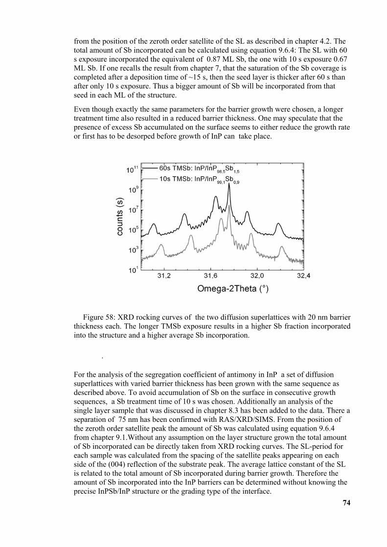
74
from the position of the zeroth order satellite of the SL as described in chapter 4.2. Thetotal amount of Sb incorporated can be calculated using equation 9.6.4: The SL with 60s exposure incorporated the equivalent of 0.87 ML Sb, the one with 10 s exposure 0.67ML Sb. If one recalls the result from chapter 7, that the saturation of the Sb coverage iscompleted after a deposition time of ~15 s, then the seed layer is thicker after 60 s thanafter only 10 s exposure. Thus a bigger amount of Sb will be incorporated from thatseed in each ML of the structure.
Even though exactly the same parameters for the barrier growth were chosen, a longertreatment time also resulted in a reduced barrier thickness. One may speculate that thepresence of excess Sb accumulated on the surface seems to either reduce the growth rateor first has to be desorped before growth of InP can take place.
Figure 58: XRD rocking curves of the two diffusion superlattices with 20 nm barrierthickness each. The longer TMSb exposure results in a higher Sb fraction incorporatedinto the structure and a higher average Sb incorporation.
.
For the analysis of the segregation coefficient of antimony in InP a set of diffusionsuperlattices with varied barrier thickness has been grown with the same sequence asdescribed above. To avoid accumulation of Sb on the surface in consecutive growthsequences, a Sb treatment time of 10 s was chosen. Additionally an analysis of thesingle layer sample that was discussed in chapter 8.3 has been added to the data. There aseparation of 75 nm has been confirmed with RAS/XRD/SIMS. From the position ofthe zeroth order satellite peak the amount of Sb was calculated using equation 9.6.4from chapter 9.1.Without any assumption on the layer structure grown the total amountof Sb incorporated can be directly taken from XRD rocking curves. The SL-period foreach sample was calculated from the spacing of the satellite peaks appearing on eachside of the (004) reflection of the substrate peak. The average lattice constant of the SLis related to the total amount of Sb incorporated during barrier growth. Therefore theamount of Sb incorporated into the InP barriers can be determined without knowing theprecise InPSb/InP structure or the grading type of the interface.
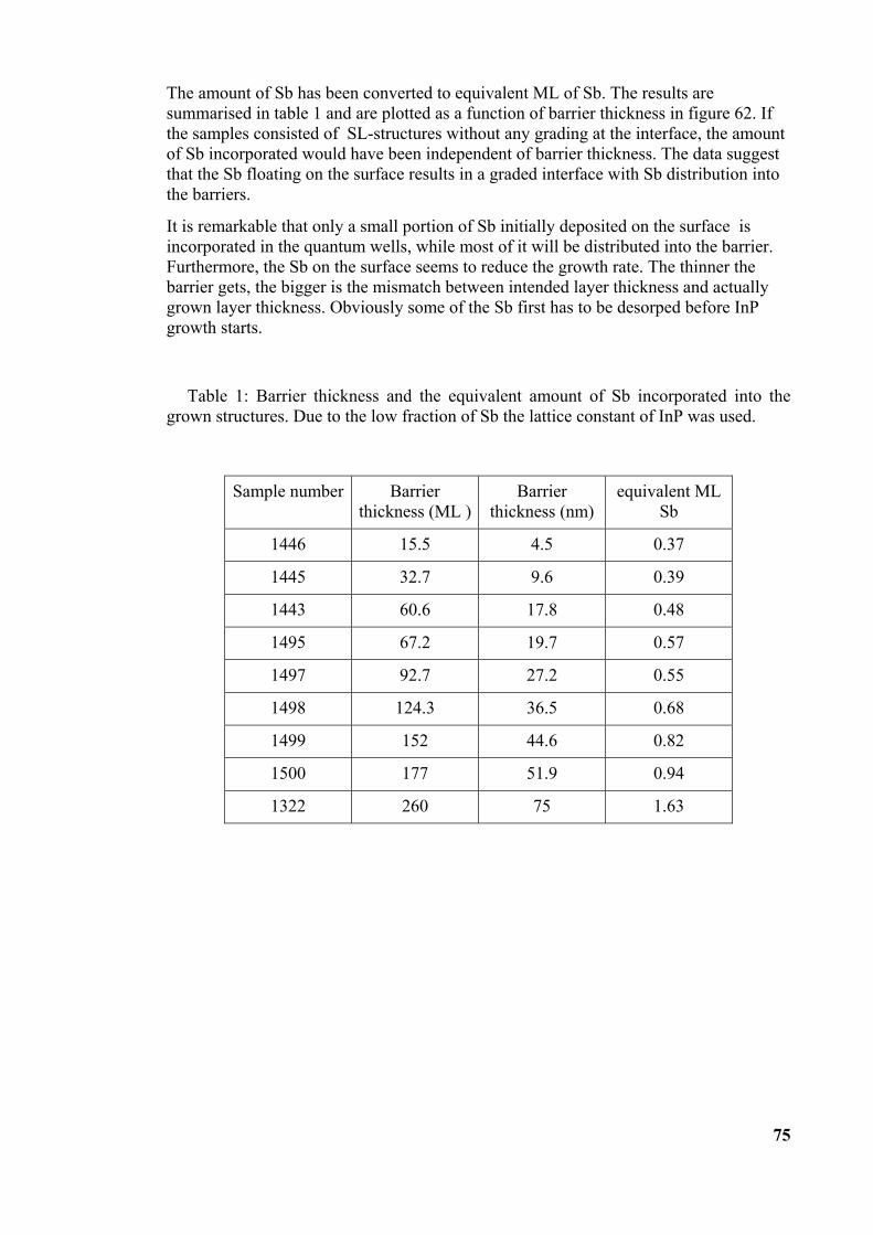
75
The amount of Sb has been converted to equivalent ML of Sb. The results aresummarised in table 1 and are plotted as a function of barrier thickness in figure 62. Ifthe samples consisted of SL-structures without any grading at the interface, the amountof Sb incorporated would have been independent of barrier thickness. The data suggestthat the Sb floating on the surface results in a graded interface with Sb distribution intothe barriers.
It is remarkable that only a small portion of Sb initially deposited on the surface isincorporated in the quantum wells, while most of it will be distributed into the barrier.Furthermore, the Sb on the surface seems to reduce the growth rate. The thinner thebarrier gets, the bigger is the mismatch between intended layer thickness and actuallygrown layer thickness. Obviously some of the Sb first has to be desorped before InPgrowth starts.
Table 1: Barrier thickness and the equivalent amount of Sb incorporated into thegrown structures. Due to the low fraction of Sb the lattice constant of InP was used.
Sample number Barrierthickness (ML )
Barrierthickness (nm)
equivalent MLSb
1446 15.5 4.5 0.37
1445 32.7 9.6 0.39
1443 60.6 17.8 0.48
1495 67.2 19.7 0.57
1497 92.7 27.2 0.55
1498 124.3 36.5 0.68
1499 152 44.6 0.82
1500 177 51.9 0.94
1322 260 75 1.63
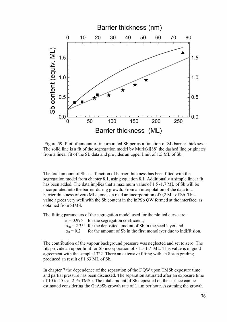
76
Figure 59: Plot of amount of incorporated Sb per as a function of SL barrier thickness.The solid line is a fit of the segregation model by Muriaki[88] the dashed line originatesfrom a linear fit of the SL data and provides an upper limit of 1.5 ML of Sb.
The total amount of Sb as a function of barrier thickness has been fitted with thesegregation model from chapter 8.1, using equation 8.1. Additionally a simple linear fithas been added. The data implies that a maximum value of 1,5 -1.7 ML of Sb will beincorporated into the barrier during growth. From an interpolation of the data to abarrier thickness of zero MLs, one can read an incorporation of 0,2 ML of Sb. Thisvalue agrees very well with the Sb content in the InPSb QW formed at the interface, asobtained from SIMS.
The fitting parameters of the segregation model used for the plotted curve are:σ = 0.995 for the segregation coefficient, xin = 2.35 for the deposited amount of Sb in the seed layer and x0 = 0.2 for the amount of Sb in the first monolayer due to indiffusion.
The contribution of the vapour background pressure was neglected and set to zero. Thefits provide an upper limit for Sb incorporation of ~1.5-1,7 ML. This value is in goodagreement with the sample 1322. There an extensive fitting with an 8 step gradingproduced an result of 1.63 ML of Sb.
In chapter 7 the dependence of the separation of the DQW upon TMSb exposure timeand partial pressure has been discussed. The separation saturated after an exposure timeof 10 to 15 s at 2 Pa TMSb. The total amount of Sb deposited on the surface can beestimated considering the GaAsSb growth rate of 1 µm per hour. Assuming the growth
77
rate of InSb to be equal, one would have grown 2,7 nm of InSb in 10 s. This equals 4,3lattice constants of InSb or 4,3 ML of elemental Sb. This amount of deposited Sb isvery high compared to the maximum of 1,5 –1,7 ML of Sb incorporated into thebarriers. Even if one considers that some of the Sb desorpes during the growthinterruption, this value is still to high. Alternatively one has to take into account that thesticking coefficient of Sb changes during deposition, as fig. 51 in chapter 8.3 suggest.Therefore 1,5 to 1,7 ML seem to be a reasonable value to be assumed as an upper limitof Sb deposition.
The value near unity obtained for the segregation coefficient is very high, meaning thatmost of the Sb floats on the surface, and only little of it will be incorporated in everysuccessive monolayer. The segregation model described above has been applied tosimulate the Sb-distribution in the SL-structures. The quantum well was assumed to beInP0.947Sb0.053 with an thickness of 1,1 nm. The Sb-content of the InPSb was taken fromthe calibrated SIMS measurements discussed in chapter 8, which assigned 4-5% of Sbin the interface layer. To simulate the grading of the Sb distribution into the InPbarriers, an exponential decay was applied as illustrated in fig 64. A reasonable fit couldonly be achieved when the Sb content in the first monolayer of the barrier was about3%, and thus less than in the QW, followed by an exponential decay to 0,1% in the lastML.
It is very simple to fit the satellite peaks with respect of the x-axis without anystructural model. But to obtain a „real fit“, additionally the height of the satellite peakshas to be considered. The position of the peaks is only determined by the total amountof Sb in the structure and the barrier thickness. The envelope function of the amplitudesof the satellite peaks is determined by the grading of the interface. The HRXRD rockingcurve and the simulation of the SL with 20 nm barrier thickness are displayed in figure64 . The heights of the satellite peaks are consistent with a long range grading of theinterface, with a very high segregation coefficient of 0,995 and a Sb ratio of about 0,3ML of Sb distributed in a ~1,1 nm thick InPSb QW at the interface.
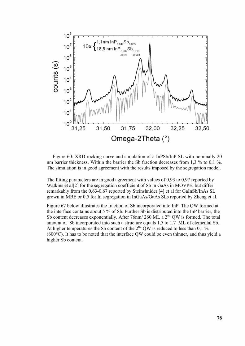
78
Figure 60: XRD rocking curve and simulation of a InPSb/InP SL with nominally 20nm barrier thickness. Within the barrier the Sb fraction decreases from 1,3 % to 0,1 %.The simulation is in good agreement with the results imposed by the segregation model.
The fitting parameters are in good agreement with values of 0,93 to 0,97 reported byWatkins et al[2] for the segregation coefficient of Sb in GaAs in MOVPE, but differremarkably from the 0,63-0,67 reported by Steinshnider [4] et al for GaInSb/InAs SLgrown in MBE or 0,5 for In segregation in InGaAs/GaAs SLs reported by Zheng et al.
Figure 67 below illustrates the fraction of Sb incorporated into InP. The QW formed atthe interface contains about 5 % of Sb. Further Sb is distributed into the InP barrier, theSb content decreases exponentially. After 76nm/ 260 ML a 2nd QW is formed. The totalamount of Sb incorporated into such a structure equals 1,5 to 1,7 ML of elemental Sb.At higher temperatures the Sb content of the 2nd QW is reduced to less than 0,1 %(600°C). It has to be noted that the interface QW could be even thinner, and thus yield ahigher Sb content.
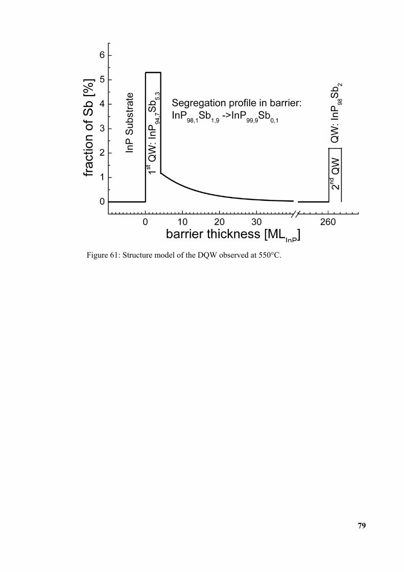
79
Figure 61: Structure model of the DQW observed at 550°C.

80
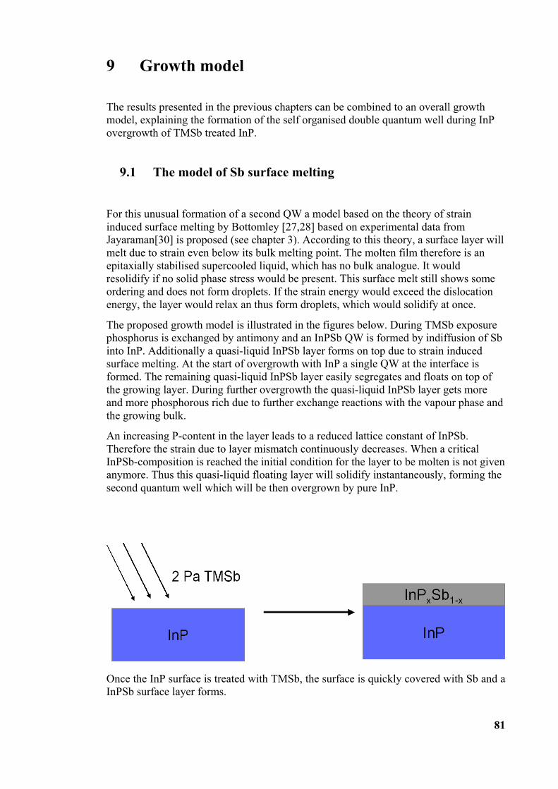
81
9 Growth model
The results presented in the previous chapters can be combined to an overall growthmodel, explaining the formation of the self organised double quantum well during InPovergrowth of TMSb treated InP.
9.1 The model of Sb surface melting
For this unusual formation of a second QW a model based on the theory of straininduced surface melting by Bottomley [27,28] based on experimental data fromJayaraman[30] is proposed (see chapter 3). According to this theory, a surface layer willmelt due to strain even below its bulk melting point. The molten film therefore is anepitaxially stabilised supercooled liquid, which has no bulk analogue. It wouldresolidify if no solid phase stress would be present. This surface melt still shows someordering and does not form droplets. If the strain energy would exceed the dislocationenergy, the layer would relax an thus form droplets, which would solidify at once.
The proposed growth model is illustrated in the figures below. During TMSb exposurephosphorus is exchanged by antimony and an InPSb QW is formed by indiffusion of Sbinto InP. Additionally a quasi-liquid InPSb layer forms on top due to strain inducedsurface melting. At the start of overgrowth with InP a single QW at the interface isformed. The remaining quasi-liquid InPSb layer easily segregates and floats on top ofthe growing layer. During further overgrowth the quasi-liquid InPSb layer gets moreand more phosphorous rich due to further exchange reactions with the vapour phase andthe growing bulk.
An increasing P-content in the layer leads to a reduced lattice constant of InPSb.Therefore the strain due to layer mismatch continuously decreases. When a criticalInPSb-composition is reached the initial condition for the layer to be molten is not givenanymore. Thus this quasi-liquid floating layer will solidify instantaneously, forming thesecond quantum well which will be then overgrown by pure InP.
Once the InP surface is treated with TMSb, the surface is quickly covered with Sb and aInPSb surface layer forms.
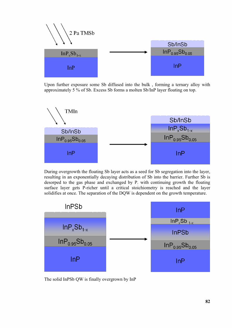
82
Upon further exposure some Sb diffused into the bulk , forming a ternary alloy withapproximately 5 % of Sb. Excess Sb forms a molten Sb/InP layer floating on top.
During overgrowth the floating Sb layer acts as a seed for Sb segregation into the layer,resulting in an exponentially decaying distribution of Sb into the barrier. Further Sb isdesorped to the gas phase and exchanged by P. with continuing growth the floatingsurface layer gets P-richer until a critical stoichiometry is reached and the layersolidifies at once. The separation of the DQW is dependent on the growth temperature.
The solid InPSb QW is finally overgrown by InP
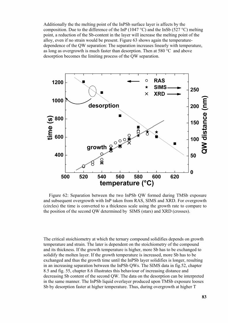
83
Additionally the the melting point of the InPSb surface layer is affects by thecomposition. Due to the difference of the InP (1047 °C) and the InSb (527 °C) meltingpoint, a reduction of the Sb-content in the layer will increase the melting point of thealloy, even if no strain would be present. Figure 63 shows again the temperature-dependence of the QW separation: The separation increases linearly with temperature,as long as overgrowth is much faster than desorption. Then at 580 °C and abovedesorption becomes the limiting process of the QW separation.
Figure 62: Separation between the two InPSb QW formed during TMSb exposureand subsequent overgrowth with InP taken from RAS, SIMS and XRD. For overgrowth(circles) the time is converted to a thickness scale using the growth rate to compare tothe position of the second QW determined by SIMS (stars) and XRD (crosses).
The critical stoichiometry at which the ternary compound solidifies depends on growthtemperature and strain. The later is dependent on the stoichiometry of the compoundand its thickness. If the growth temperature is higher, more Sb has to be exchanged tosolidify the molten layer. If the growth temperature is increased, more Sb has to beexchanged and thus the growth time until the InPSb layer solidifies is longer, resultingin an increasing separation between the InPSb QWs. The SIMS data in fig.52, chapter8.5 and fig. 55, chapter 8.6 illustrates this behaviour of increasing distance anddecreasing Sb content of the second QW. The data on the desorption can be interpretedin the same manner. The InPSb liquid overlayer produced upon TMSb exposure loosesSb by desorption faster at higher temperature. Thus, during overgrowth at higher T
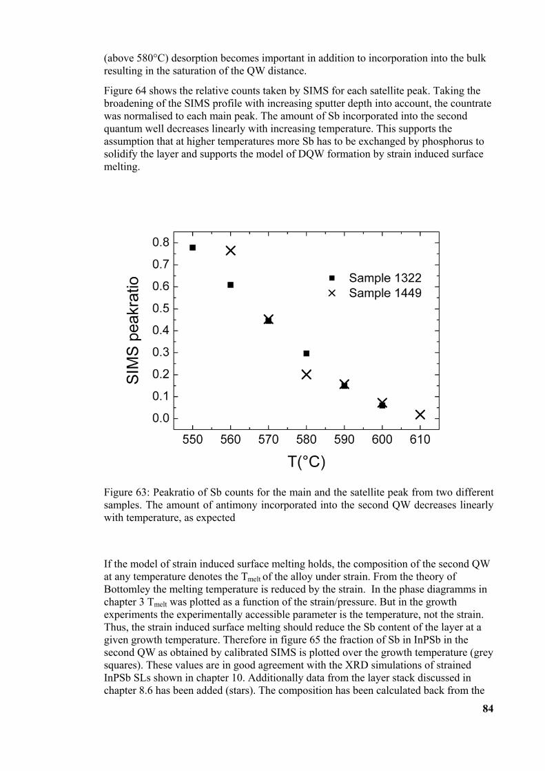
84
(above 580°C) desorption becomes important in addition to incorporation into the bulkresulting in the saturation of the QW distance.
Figure 64 shows the relative counts taken by SIMS for each satellite peak. Taking thebroadening of the SIMS profile with increasing sputter depth into account, the countratewas normalised to each main peak. The amount of Sb incorporated into the secondquantum well decreases linearly with increasing temperature. This supports theassumption that at higher temperatures more Sb has to be exchanged by phosphorus tosolidify the layer and supports the model of DQW formation by strain induced surfacemelting.
Figure 63: Peakratio of Sb counts for the main and the satellite peak from two differentsamples. The amount of antimony incorporated into the second QW decreases linearlywith temperature, as expected
If the model of strain induced surface melting holds, the composition of the second QWat any temperature denotes the Tmelt of the alloy under strain. From the theory ofBottomley the melting temperature is reduced by the strain. In the phase diagramms inchapter 3 Tmelt was plotted as a function of the strain/pressure. But in the growthexperiments the experimentally accessible parameter is the temperature, not the strain.Thus, the strain induced surface melting should reduce the Sb content of the layer at agiven growth temperature. Therefore in figure 65 the fraction of Sb in InPSb in thesecond QW as obtained by calibrated SIMS is plotted over the growth temperature (greysquares). These values are in good agreement with the XRD simulations of strainedInPSb SLs shown in chapter 10. Additionally data from the layer stack discussed inchapter 8.6 has been added (stars). The composition has been calculated back from the
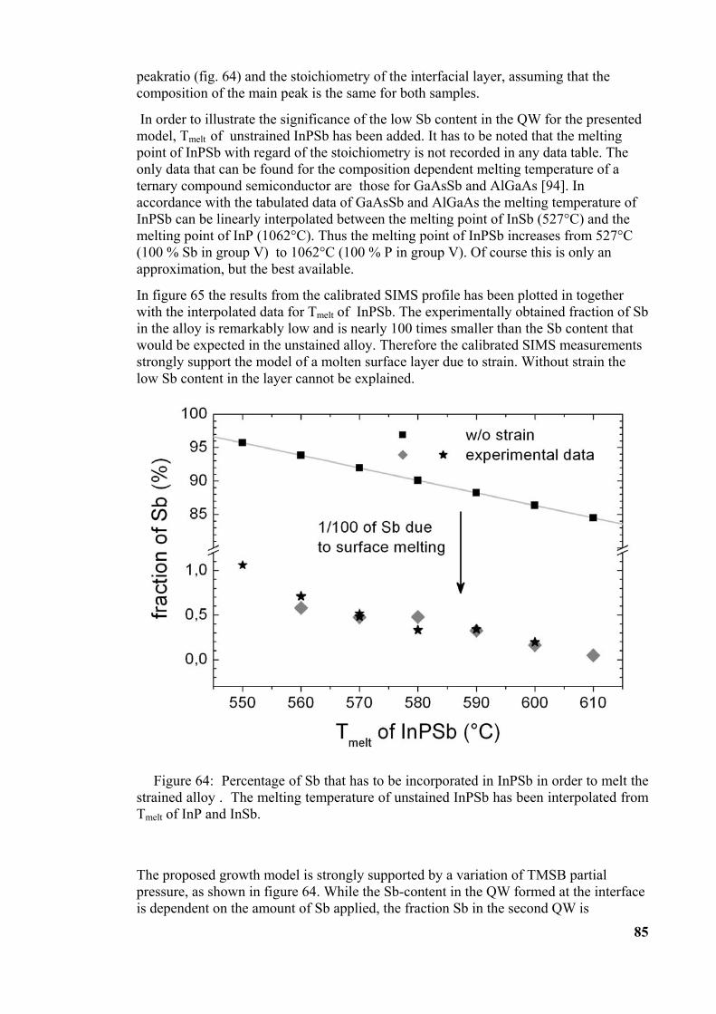
85
peakratio (fig. 64) and the stoichiometry of the interfacial layer, assuming that thecomposition of the main peak is the same for both samples.
In order to illustrate the significance of the low Sb content in the QW for the presentedmodel, Tmelt of unstrained InPSb has been added. It has to be noted that the meltingpoint of InPSb with regard of the stoichiometry is not recorded in any data table. Theonly data that can be found for the composition dependent melting temperature of aternary compound semiconductor are those for GaAsSb and AlGaAs [94]. Inaccordance with the tabulated data of GaAsSb and AlGaAs the melting temperature ofInPSb can be linearly interpolated between the melting point of InSb (527°C) and themelting point of InP (1062°C). Thus the melting point of InPSb increases from 527°C(100 % Sb in group V) to 1062°C (100 % P in group V). Of course this is only anapproximation, but the best available.
In figure 65 the results from the calibrated SIMS profile has been plotted in togetherwith the interpolated data for Tmelt of InPSb. The experimentally obtained fraction of Sbin the alloy is remarkably low and is nearly 100 times smaller than the Sb content thatwould be expected in the unstained alloy. Therefore the calibrated SIMS measurementsstrongly support the model of a molten surface layer due to strain. Without strain thelow Sb content in the layer cannot be explained.
Figure 64: Percentage of Sb that has to be incorporated in InPSb in order to melt thestrained alloy . The melting temperature of unstained InPSb has been interpolated fromTmelt of InP and InSb.
The proposed growth model is strongly supported by a variation of TMSB partialpressure, as shown in figure 64. While the Sb-content in the QW formed at the interfaceis dependent on the amount of Sb applied, the fraction Sb in the second QW is
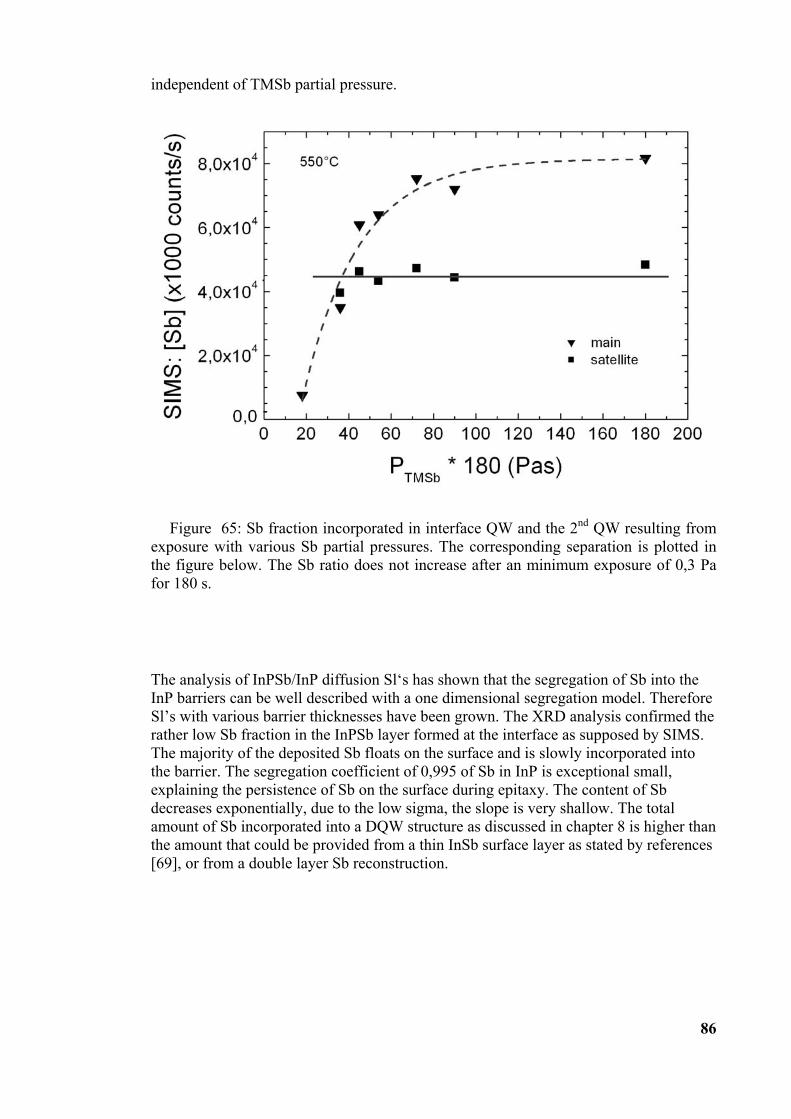
86
independent of TMSb partial pressure.
Figure 65: Sb fraction incorporated in interface QW and the 2nd QW resulting fromexposure with various Sb partial pressures. The corresponding separation is plotted inthe figure below. The Sb ratio does not increase after an minimum exposure of 0,3 Pafor 180 s.
The analysis of InPSb/InP diffusion Sl‘s has shown that the segregation of Sb into theInP barriers can be well described with a one dimensional segregation model. ThereforeSl’s with various barrier thicknesses have been grown. The XRD analysis confirmed therather low Sb fraction in the InPSb layer formed at the interface as supposed by SIMS.The majority of the deposited Sb floats on the surface and is slowly incorporated intothe barrier. The segregation coefficient of 0,995 of Sb in InP is exceptional small,explaining the persistence of Sb on the surface during epitaxy. The content of Sbdecreases exponentially, due to the low sigma, the slope is very shallow. The totalamount of Sb incorporated into a DQW structure as discussed in chapter 8 is higher thanthe amount that could be provided from a thin InSb surface layer as stated by references[69], or from a double layer Sb reconstruction.
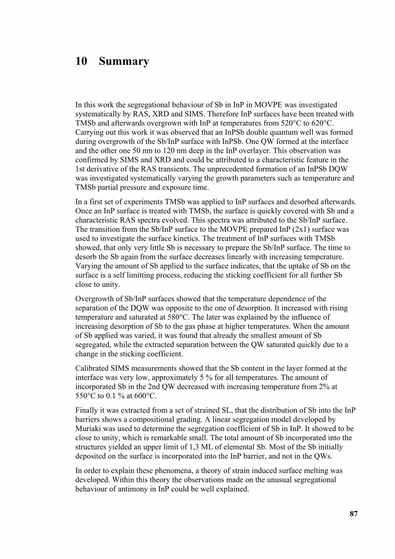
87
10 Summary
In this work the segregational behaviour of Sb in InP in MOVPE was investigatedsystematically by RAS, XRD and SIMS. Therefore InP surfaces have been treated withTMSb and afterwards overgrown with InP at temperatures from 520°C to 620°C.Carrying out this work it was observed that an InPSb double quantum well was formedduring overgrowth of the Sb/InP surface with InPSb. One QW formed at the interfaceand the other one 50 nm to 120 nm deep in the InP overlayer. This observation wasconfirmed by SIMS and XRD and could be attributed to a characteristic feature in the1st derivative of the RAS transients. The unprecedented formation of an InPSb DQWwas investigated systematically varying the growth parameters such as temperature andTMSb partial pressure and exposure time.
In a first set of experiments TMSb was applied to InP surfaces and desorbed afterwards.Once an InP surface is treated with TMSb, the surface is quickly covered with Sb and acharacteristic RAS spectra evolved. This spectra was attributed to the Sb/InP surface.The transition from the Sb/InP surface to the MOVPE prepared InP (2x1) surface wasused to investigate the surface kinetics. The treatment of InP surfaces with TMSbshowed, that only very little Sb is necessary to prepare the Sb/InP surface. The time todesorb the Sb again from the surface decreases linearly with increasing temperature.Varying the amount of Sb applied to the surface indicates, that the uptake of Sb on thesurface is a self limitting process, reducing the sticking coefficient for all further Sbclose to unity.
Overgrowth of Sb/InP surfaces showed that the temperature dependence of theseparation of the DQW was opposite to the one of desorption. It increased with risingtemperature and saturated at 580°C. The later was explained by the influence ofincreasing desorption of Sb to the gas phase at higher temperatures. When the amountof Sb applied was varied, it was found that already the smallest amount of Sbsegregated, while the extracted separation between the QW saturated quickly due to achange in the sticking coefficient.
Calibrated SIMS measurements showed that the Sb content in the layer formed at theinterface was very low, approximately 5 % for all temperatures. The amount ofincorporated Sb in the 2nd QW decreased with increasing temperature from 2% at550°C to 0.1 % at 600°C.
Finally it was extracted from a set of strained SL, that the distribution of Sb into the InPbarriers shows a compositional grading. A linear segregation model developed byMuriaki was used to determine the segregation coefficient of Sb in InP. It showed to beclose to unity, which is remarkable small. The total amount of Sb incorporated into thestructures yielded an upper limit of 1,3 ML of elemental Sb. Most of the Sb initiallydeposited on the surface is incorporated into the InP barrier, and not in the QWs.
In order to explain these phenomena, a theory of strain induced surface melting wasdeveloped. Within this theory the observations made on the unusual segregationalbehaviour of antimony in InP could be well explained.

88
89
11 Bibliography
[1] H. Kroemer, Physica E, 20, 196-203 (2004)
[2] M. W. Dvorak, C.R. Bolognesi, O.J. Pitts, S.P. Watkins, IEEE Electron DeviceLett., 22 (2001)
[3] O.J. Pitts, S.P. Watkins, C.X. Wang, V. Fink, K.L. Kavanagh, J. Chrys. Growth 254,28-34 (2003)
[4] J. Steinshnider, J. Harper, M. Weimer, C.-H. Lin, S. S. Pei, D.H. Chow, Phys. Rev.Lett 85, 4562 (2000)
[5] R. Kaspi J. Chryst. Growth 201/202, 864 (1999)
[6] H. Jürgensen, Large scale MOVPE production systems119, MicroelectronicEngineering 18 (1992)
[7] Aixtron company, "Aixtron 3000", http://www.aixtron.com
[8] I. M. Manasevit, Appl. Phys. Lett. 12, 156 (1968)
[9] R. M. Biefeld, Materials Science and Engineering, R 36, 105-142 (2002)
[10] A. Aardvaark, N. J. Mason, P. J. Walker, Prog. Crystal Growth and Charact., Nos.2-4, 207-241 (1997)
[11] F. Dimroth, C. Augert, A. W. Bett, J. Chrystal Growth, 248, 263 - 273 2003,
[12] J. Hu, X. G. Xu, J. A. H. Stotz, S. P. Watkins, A. E. Curzon, M. L. W. Thewalt, N.Matine, and C. R. Bolognesi, Appl. Phys. Lett., 73, 2799 (1998)
[13] M. Peter, N. Herres, F. Fuchs, K. Winkler, K.-H. Bachem, and J. Wagner, Appl.Phys. Lett. 74, 410 (1999)
[14] Sakaki H. Sakaki, L.L. chang, R. Ludeke, C. A. Chang, G. A. Sai-Halasz, L.Esaki, Appl. Phys. Lett 31, 211 (1977)
[15] Paulo V. Santos, P. Etchegoin, M. Cardona, B. Brar, H. Kroemer, Phys. Rev B 50,12 (1994)
[16] B. V. Shanabrook, W. Barvosa-Carter, R. Bass, B. R. Bennett, J. B. Boos, W. W.Bewley, A. S. Bracker, J. C. Culbertson, E. R. Glaser, W. Kruppa, R. Magno, W.J. Moore, J. R. Meyer, B. Z. Nosho, D. Park, P. M. Thibado, M. E. Twigg, R. J.Wagner, J. R. Waterman, L. J. Whitman and M. J. Yang, EngineeredHeterostructures of 6.1 Å III-V Semiconductors for Advanced Electronic andOptoelectronic Applications, Naval Research Labarotory, Washington D.C
[17] H. M. Manasevit and W.I. Simpson , J. Electrochem. Soc., 116, 1725 (1969)
[18] MOVPE Patent W. Miederer, G.Ziegler, R. Dötzer, Dt. Patent Nr. 1176102,Siemens, Berlin-Erlangen, 1962/1964,
[19] M. A. Herman, W. Richter und H. Sitter, Epitaxy - physical principles andtechnical implementation, Springer Verlag, Berlin, 2003
90
[20] G.B. Stringfellow, Organometallic Vapour Phase Epitaxy: Theory and Practise,Academic Press, San Diego (1989)
[21] M. Razegi, The MOCVD challenge 1, A. Hilger, Bristol, Philadelphia, (1989)
[22] M. Zorn, Optical in-situ studies and on-line growth control of binary and ternaryIII-V semiconductors with respect to the (001) surfaceDissertationTechnischeUniversität Berlin 1999 ISBN 3-89820-004-3
[23] K. Knorr, Untersuchungen von Grenzflächenprozessen bei der metallorganischenGasphasenepitaxie von III-V-HalbleiternBerlinTechnische Universität Berlin1997
[24] I. Langmuir, J. Am. chem. soc. 41, (1918)
[25] R. Brdicka, Grundlagen der Physikalischen Chemie
[26] I. N. Stranski and L. von Krastanow, , Akad. Wiss. Lit. Mainz Math. _Natur. LlIIb, 146, 797 (1939)
[27] D. J. Bottomley, Jpn. J. Appl. Phys., Vol. 37, 2652-2655 (1998)
[28] D. J. Bottomley, Jpn. J. Appl. Phys, 36, L1464 1997,
[29] Bottomly 2000D. J. Bottomley,Jpn. J. Appl. Phys.,394604-4608 (2000)
[30] A. Jayaraman, W. Klement, Jr. and G.C Kennedy, Phys. Rev, 130, 540 (1963)
[31] P. W. Atkins. Physical Chemistry. Oxford University Press, 1997
[32] I. Barin, Thermochemical Data of Pure Substances, Wiley-VCH, 1998
[33] J. Hornstra and W. J. Bartels, J. Chryst Growth, 44, 513 (1978)
[34] M. Cardona, F. Pollack, and K. Shaklee, J. Phys. Soc. Jpn. Suppl, 21, 89 (1966)
[35] W. Richter, Appl. Phys. A , 75, 129-140 (2002)
[36] J. Rumberg, Development and Optimization of the Reflectance AnisotropySpectroscopy (RAS) with Respect to Online Growth Control, Band DiplomaThesis, Technische Universität Berlin, (1995)
[37] W. Richter and J.T. Zettler, Appl. Surf. Sci, 100-101, 496 (1996)
[38] W. Richter, Phil. Trans. R. Soc, A 344, 453 (1993)
[39] M. Pristovsek, T. Trepk, M. Klein, J.-T. Zettler, W. Richter J. Appl. Phys. 87,1245-1250 (2000)
[40] M. PristovsekFundamental Growth Processes on Different Gallium ArsenideSurfaces in Metal-Organic Vapour Phase EpitaxyDissertationTechnischeUniversität Berlin 2000
[41] I. Kamiya, D. E. Aspnes, H. Tanaka, L. T. Florez, J. P. Harbison, and R. Bhat,Phys. Rev. Lett. 68627 (1992)
[42] C. Kaspari, M. Pristovsek, W. Richter, phys. stat. sol., 13, 242, 2561-2569 (2005)
[43] X’Pert Epitaxy, wwv.pananalytical.com
91
[44] Esser, W.G. Schmidt, J. Bernholc, A.M. Frisch, P. Vogt, M. Zorn, M. Pristovsek,W. Richter, F. Bechstedt, Th. Hannappel, Visbeck, J. Vac. Sci. Technol. B 17,1691 (1999)
[45] M. Itoh, G. R. Bell, A. R. Avery, T. S. Jones, B. A. Joyce, and D. D. Vvedensky,Phys. Rev. Lett. 81, 633 (1998)
[46] W. A Harrisson, J. Vac. Sci. Technol., 16, 1492 (1979)
[47] P.Vogt , Atomic structure of the (001) surfaces of InP, GaP and InGaP, TUBerlin,Wissenschaft und Technik Verlag, Berlin 2002
[48] O. Pulci, K. Lüdge, P. Vogt, N. Esser, W. G. Schmidt, W. Richter, and F.Bechstedt, Comp. Mat. Sci. 22, 32 (2001)
[49] L. J. Whitman, P. M. Thibado, S. C. Erwin, B. R. Bennett, and B. V. Shanabrooke,Phys Rev. Lett. 79, 693 (1997)
[50] C.F. McConville, T.S. Jones, F.M. Leibsle, S.M. Driver, T.C.Q. Noakes, M.O.Schweitzer, N.V. Richardson, Phys. Rev. B 50, 14965 (1994)
[51] Waterman Sb J. R. Waterman, B. V. Shanabrook, and R. J. Wagner, J. Vac. Sci.Technol. B, 10, 895 (1992)
[52] Sieger Sb M. T. Sieger, T. Miller, and T. C. Chiang , Phys. Rev B 52, 8256(1995)
[53] U. Resch-Esser, N. Esser, B. Brar, H. Kroemer, Phys. Rev. B 55, 15401-15404(1997)
[54]. M. Thibado, B.R Bennett, B.V. Shanabrook,L.J. Whitman, J. Chryst. Growth, 175- 176, 317 (1996)
[55] G. E. Franklin D. H. Rich, A. Samsavar, E. S. Hirschorn, F. M. Leibsle, T. Miller,and T.-C. Chiang., Phys. Rev. B 41, 12619 (1990)
[56] Z. Nosho, B. V. Shanabrook, B. R. Bennett, W. Barvosa-Carter, W. H. Weinberg,L. J. Whitman, Surf. Sci. 478, 1-8 (2001)
[57] W. Barvosa-Carter, A. S. Bracker, J. C. Culbertson, B. Z. Nosho, B. V.Shanabrook, L. J. Whitmann, Hanchul Kim, N. A. Modine, E. Kaxiras Phys.Rev. Lett. 84, 4649 (2000)
[58] C. Kumpf, D. Smilgies, E. Landmark, M. Nielsen, R. Feidenhans, O. Bunk, J. h.Zeysing, Y. Su, R. L. Johnson, L. Cao, J. Zegenhagen, B. O. Finland, L. D.Marks, D. Ellis, Phys. Rev. B 64, 076307 (2001)
[59] T. D. Mishima, N. Naruse, S. P. Cho, T. Kadohira, T. Osaka, Phys. Rev. Lett. 89,276105 (2002)
[60] Kollonitsch, H.-J. Schimper, U. Seidel, K. Möller, S. Neumann, F.-J. Tegude, F.Willig, T. Hannappel, J. Crys. Growth 285, 36-540 (2006)
[61] P. Soukiassian, P. S. Mangat, Y, Huttel,Z. Hurych, B. Gruzza, A. Porte , J. Vac.Sci. Technology , B 11(4) (1993)
[62] D. Rioux, H. Höchst, Phys. Rev. B, 11 (1992)
92
[63] G. Hollinger, D. Gallet, M. Gendry, C. Santinelli, P. Viktorovitch, J. Vac. Sci.Technol B, 8, 832 (1990)
[64] M. Naganuma, S. Miyazawa, H. Iwaski, J. Vac. Sci. Technol. 17, 606 (1980)
[65] O.J. Pitts, S.P. Watkins, C.X. Wang, V. Fink, K.L. Kavanagh, J. Crystal Growth254 ,28 (2003)
[66] C.X. Wang, O.J. Pitts, S.P. Watkins, J. Crystal Growth, 248, 8 (2003)
[67] F. Brunner, S. Weeke, M. Zorn, M. Weyers, J. Crystal Growth, 221, (2004)
[68] Möller, Z. Kollonitsch, Ch. Giesen, M. Heuken, F. Willig, T. Hannappel, J. CrystalGrowth 248, 244 (2003)
[69] Y. Sun, S. F. Cheng, G. Chen, R. L. Woo, R. F. Hicks, J. Appl. Phys 97, (2005)
[70] W. K. Liu and M. B. Santos, Surf. Sci. 319, 172 (1994)
[71] C.X. Wang, O.J. Pitts, S.P. Watkins, J. Crystal Growth, 248, 259 (2003)
[72] Pristovsek, M. Zorn, U. Zeimer, M. WeyersJ. Crystal Growth 276, 347 (2005)
[73] O.J. Pitts, S.P. Watkins, C.X. Wang, J.A.H. Stotz, M.L.W. Thewalt, J. Electron.Mater.30, 1412 (2001)
[74] O.J. Pitts, S.P. Watkins, C.X. Wang, J. Crys. Growth, 248, 249 (2003)
[75] G. Schmidt, P. H. Hahn, F. Bechstedt, N. Esser, P. Vogt, A. Wange, W. RichterPhys. Rev. Lett. 90 126121 (2003)
[76] M. Pristovsek, B. Han, J.-T. Zettler, W. Richter, J. Crys. Growth 221, 149-155(2000)
[77] J. K. Shurtleff, R.T. Lee, G.B. Stringfellow, IEEE 2000
[78] J. J. Zinck, E. J. Tarsa, B. Brar, J. S. Speck, J. Appl. Phys. 82, 6067 (1997)
[79] E. Kessler, Phys. stat. solidi A, K61, (1989)
[80] T.W. Lee, H. Hwang, Y. Moon, and E. Yoon, J. Vac. Sci. Technol. A, 17, 2663(1999)
[81] J. Jönsson, F. Reinhardt, M. Zorn, K. Ploska, W. Richter, J. Rumberg, Appl. Phys.Lett. 64 (1994)
[82 ] V.K. Paliwal and S. M. Shivaprasad, Surf. Sci. 561, L207-L212 (2004)
[83] F. Maeda, Y. Watanabe, and M. Oshima, Phys. Ref. Letters 78, 4233-4236 (1997)
[84] F. Maeda and Y. Watanabe, J. of Electron Microscopy and related phenomena, 88-91, 779-785 (1998)
[85] Y.W. Mo., Phys. Rev. Lett. 71, 2923-2926 (1993)
[86] T.W. Lee, H. Hwang, Y. Moon, and E. Yoo, J. Vac. Sci. Technol. A, 17, 2663-2666 8 (2002)
[87] F. Nützel and G. Abstreiter, Phys. Ref. B 53 ,13551 (1996)
[88] K. Muriaki, Appl. Phys. Lett. 61, (1992)

93
[89] Poser GaAsN/GaAs V. Hoffmann, F. Poser, C. Kaspari, S. Weeke, M. Pristovsek,W. Richter, J. Chrys. Growth 272, 30-36 (2004)
[90] Y. Kwon, M. H. Cho, P. Moon, H. J. Kim, H. Na, H. C. Seo, H. J. Kim, Y. Shin, D.W. Moon, Y. Sun, Y. H. Cho, E. Yoon, Phys. Stat. Sol. 201, 2818 (2004)
[91] J. M. Moison, C. Guille, F. Houzay, F. Barthe, and M. Van Rompay, Phys. Rev. B,406149 (1989)
[92] Zhangade Lin, F. Xu, and J. H. Weaver, Phys. Ref. B 115, 777 (1987)
[93] J. F. Zheng, J. D. Walker, M. B. Salmeron, E. R. Weber, Phys. Ref. Lett. 72, 2414– 2417 (1994)
[94] Goldberg Yu.A. and N.M. Schmidt, Handbook Series on SemiconductorParameters, vol 2, London World Scientific (1999)