Embed Size (px)
Citation preview
AAllmmaa MMaatteerr SSttuuddiioorruumm –– UUnniivveerrssiittàà ddii BBoollooggnnaa
DOTTORATO DI RICERCA IN
Scienze Chimiche
Ciclo XXVII
Settore Concorsuale di afferenza: 03/B1 Settore Scientifico disciplinare: CHIM/03
Development of synthetic methods of silicon nanocrystals functionalized with
photoactive molecules
Presentata da: Mirko Locritani
Coordinatore Dottorato Relatore
Prof. Aldo Roda Prof. Paola Ceroni
Esame finale anno 2015
Contents Preface
List of abbreviations
Part I
Chapter 1 Introduction
1.1 Silicon
1.2 Semiconductors from point of view of band theory
1.3 Doping of semiconductors
1.4 Optical properties of semiconductors
1.5 Defects in the crystal structure
1.6 Silicon nanocrystals or silicon quantum dots
Part II
Chapter 2 Synthetic methods
2.1 Techniques for the synthesis of silicon nanocrystals
2.2 SiNCs in solid matrices
2.3 Colloidal SiNCs
2.4 Production methods
2.5 Chemical methods
2.5.1 Chemical solution-based synthesis
2.5.2 Thermal degradation in supercritical fluids
2.5.3 Silicon nanopowder from SiOx
2.6 Physico-chemical methods
2.6.1 Laser induced SiH4 pyrolysi
Part III
Chapter 3 Techniques for the characterization of silicon nanocrystals
3.1 Introduction
3.2 X-ray diffraction (XRD)
3.3 ATR-FTIR spectroscopy
3.4 X-ray photoelectronspectroscopy (XPS)
3.5 Nuclear magnetic resonance analysis (NMR)
3.6 Trasmission electron microscopy (TEM)
3.7 Photophysical Techniques
Part IV
Chapter 4 Silicon nanocrystals functionalized with pyrene units: efficient light-
harvesting antennae with bright near-infrared emission
4.1 Introduction
4.2 Synthesis of oxide-embedded silicon nanocrystals of different sizes
4.3 Liberation of hydride-terminated-SiNCs from silica matrix
4.4 Covalent functionalization of SiNCs with pyrene units
4.5 Results and discussion
4.6 Conclusion
Part V
Chapter 5 Interaction between pyrene-functionalized Silicon nanocrystals and
carbon allotropes
5.1 Introduction
5.2 Thermal hydrosililation of SiNCs with 1-(allyloxymethyl)pyrene (C3) and 1-
((undec-10-en-1-yloxy)methyl)pyrene (C11)
5.2.1 Experimental details
5.3 Material characterization

5.4 Results and Discussion
5.5 Interaction of silicon nanocrystals with carbon-based materials
5.5.1 Interaction of SiNC(C11)Py with C60
5.5.2 Interaction of SiNC(C11)Py with SWCNTs
5.5.3 Interaction of SiNC(C11)Py with graphene
5.6 Conclusion
Part VI
Chapter 6 Silicon nanocrystals and zinc push-pull tetraphenyl porphyrins
6.1 Introduction
6.2 Covalent passivation of SiNCs with ZnTPP
6.2.1 Experimental details
6.3 Material characterization
6.4 Results and Discussion
6.5 Conclusion
Part VII
Chapter 7 Silicon nanocrystals with thiadiazole
7.1 Introduction
7.2 Covalent passivation of SiNCs with thiadiazole
7.2.1 Experimental details
7.3 Results and Discussion
Perspectives List of Publications
Preface The object of this thesis is the development of a synthetic method for the synthesis of silicon
nanocrystals and covalent functionalization with chromophores. Part of the work concerns the
photophysical and photochemical investigation of semiconductor nanocrystals.
The thesis is divided in different parts.
Chapter 1 introduces the basic properties of semiconductors and the effect of quantum
confinement effect on optical properties reducing the size of semiconductors.
Chapter 2 describes different synthetic methods for the synthesis of silicon nanocrystals available
in literature.
Chapter 3 illustrates techniques used to characterize and investigate the systems reported in this
thesis.
Chapter 4 focuses on the synthetic method for the synthesis of silicon nanocrystals developed in
University of Texas at Austin in collaboration with Professor Brian A. Korgel.
In Chapter 5 is reported the interaction of functionalized silicon nanocrystal with carbon allotropes.
Chapter 6 concerns the interaction of silicon nanocrystals with zinc porphyrin.
Chapter 7 describes the functionalization of silicon nanocrystals with thiadiazole.
The research project was financed by European Research Council by ERC Starting Grant: PhotoSi
and University of Bologna.

List of abbreviations CVD: chemical vapor deposition
CB: conduction band
cSi: crystalline silicon
d: diameter
FS-nc-Si: free standing nanocrystalline silicon
FWHM: full width half maximum
HPLC: high performance liquid chromatography
HR-TEM: high resolution trasmission electron microscopy
HSQ: hydrogen silsesquioxane
porSi: porous silicon
PL: photoluminescence
QD: quantum dots
QY: quantum yield
SAED: selection area electron diffraction
Si: silicon
SiNCs: silicon nanocrystals
SiQDs: silicon quantum dots
SWCNT: single wall carbon nanotube
τ: lifetime
TEM: trasmission electron microscopy
VB: valence band
XRD: x-ray diffraction

Chapter 1 Introduction
1.1 Silicon
Silicon (Si) is a chemical element with atomic number 14 present in the IVA group of the periodic
table, along the bold line that separates metals from non-metals (Figure 1.1). It belongs to the p-
block with configuration (1s22s22p63s23p2), can donates or shares four valence electrons to form
bonds like carbon and manifests sp3-hybridization.
Figure 1.1
It was discovered by Antoine Lavoisier1 in 1787 but the present name was coined by Thomas
Thomson2, he believed that silicon was a nonmetal similar to boron and carbon.
After the oxygen, silicon is the most abundant element in the Earth’s crust, it is widely distributed
in dusts, sands and planets as various forms of silicon dioxide (silica) or silicates.
It is the raw material to produce glass, cement, ceramics and synthetic polymers as silicones.
1 Lavoisier, Traité Élémentaire de Chimie, (Paris, France: Cuchet, 1789), vol. 1, page 17.
2 Thomas Thomson, A System of Chemistry in Four Volumes, 5th ed., 1817, vol. 1.
Silicon has a big impact on the modern world economy for its properties as semiconductor in fact
it is at the basis of the microelectronic industry that requires a high degree of purity.
Silicon is a classic example of indirect semiconductor with band gap of 1.12 eV at room
temperature.
At present, single-crystal silicon (mc-Si) is the main material of microelectronic technology, is used
to produce a variety of semiconductor devices from diodes and transistors to extremely complex
integrated circuits and processors.
In addition, the high photosensitivity of silicon (the change of electrical conductivity under
illumination) is widely used, which allows one to convert light energy into electrical energy. This
effect is used in silicon solar cells and photodetectors.
However, the reverse process, for instance efficient conversion of electrical energy into visible
light in silicon devices has so far failed. This is connected with the peculiarities of the electronic
properties of silicon.
1.2 Semiconductors from point of view of band theory
From to the study of Ashcroft and Mermin3, solid-state materials can be classified as electrical
conductors (usually metals), semiconductors and insulators according to the nature of electrical
conductivity.
The electronic structure of these “bulk” materials, can be described using the band theory. An
electronic band is defined as a combination of atomic orbitals that constituted the material.
This band can be visualized as dense series of molecular orbitals, generated by linear combination
of atomic orbital.
A simple way to explain the above concept is to consider a solid material as an indefinitely large
assembly of atoms.4
An atom is described by molecular orbitals (Figure 1.2 a): HOMO (highest occupied molecular
orbital) and LUMO (lowest unoccupied molecular orbital).
A small cluster of several atoms of a semiconductor (Figure 1.2 b), is characterized by a
combination of atomic orbitals, with a series of occupied low-energy levels and empty high-energy
levels for excited electrons.
When increases the number of atoms in the cluster, the discrete orbitals overlap forming two
bands structure that represent a continuum (Figure 1.2 c).
Valence band (VB) is formed by bonding molecular orbitals (HOMO) and conduction band (CB) is
constituted by non-bonding molecular orbitals (LUMO).
3 N. W. Ashcroft, N. D. Mermin, Solid State Physics, 1976.
4 V. Balzani, P. Ceroni, A. Juris, Photochemistry and Photophysics, 2014, Wiley.

Figure 1.2
The energy difference between VB and CB is called energy gap Eg. The materials are classified
conductors, semiconductors and insulator as a function of this energy gap (Figure 1.3).
Figure 1.3
To understand the properties of these materials is essential to evaluate the Fermi level5 usually
denote by μ or EF. For an intrinsic semiconductor, the Fermi level can be considered as an
5 Kittel, Charles. Introduction to Solid State Physics, 1980, 7th Edition. Wiley.
hypothetical energy level of electron, such that at thermodynamic equilibrium this energy level
have a 50 % probability of being occupied.
The location of Fermi level in the band structure of material is important to determine the
electrical behavior.
In an insulator, µ lies within a large band gap, far away from any levels while in a metal µ lies
within a delocalized band.
In a semiconductor the Fermi level is located between the uppermost level of the valence band
and the lowest level of the conduction band.
1.3 Doping of semiconductors The Fermi level is also involved in the doping of semiconductors, a process of controlled addition
of impurities (defects) that changes the electrical conductivity.
There are two types of dopants:
- donors that generate free electrons in a crystal and lead to n-type semiconductors;
- acceptors that create holes with formation of p-type semiconductors.
For instance, when trivalent boron replaces a silicon atom in the crystal, a vacant state "hole" is
created, which can move around the lattice and functions as a charge carrier. This is a p-doped
silicon.
In the case of n-doped silicon, the energy needed to move the extra electron to the conduction
band (0.045eV) is comparable to kbT at room temperature.
Therefore, thermal energy will be capable of ionizing the impurity, thereby causing an increase in
the electron density in the CB, so that the Fermi level moves closer to the CB.
The doping of semiconductors finds application in the solar cell6, where electrons flow toward the
holes at the interface between n-type and p-type materials (Figure 1.4).
6 V. Balzani, P. Ceroni, A. Juris, Photochemistry and Photophysics, 2014, p. 402, Wiley.
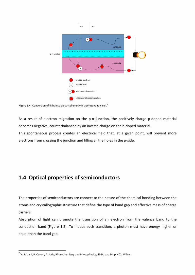
Figure 1.4 Conversion of light into electrical energy in a photovoltaic cell.7
As a result of electron migration on the p-n junction, the positively charge p-doped material
becomes negative, counterbalanced by an inverse charge on the n-doped material.
This spontaneous process creates an electrical field that, at a given point, will prevent more
electrons from crossing the junction and filling all the holes in the p-side.
1.4 Optical properties of semiconductors
The properties of semiconductors are connect to the nature of the chemical bonding between the
atoms and crystallographic structure that define the type of band gap and effective mass of charge
carriers.
Absorption of light can promote the transition of an electron from the valence band to the
conduction band (Figure 1.5). To induce such transition, a photon must have energy higher or
equal than the band gap.
7 V. Balzani, P. Ceroni, A. Juris, Photochemistry and Photophysics, 2014, cap 14, p. 402, Wiley.

Figure 1.4 Principal electronic processes: 1 excitation, 2 radiative or non radiative decay of free carriers, 3 charge trapping, 4
radiative and nonradiative recombination of trapped charge carriers. Reproduced from Ref.8
The result is the electron-hole pair, called exciton,9 a bound state due to the electrostatic Coulomb
force between the electron and the hole.
After thermal relaxation into free electrons and holes, these charge carriers can either recombine
by nonradiative or radiative processes or can be trapped by defects present in the crystal structure.
The width of the intrinsic band gap in the semiconductor (undoped), is very important because it
allows to observe the luminescence, preventing the rapid deactivation of the electron-hole charge
carriers.
As for molecules, the photon absorption is regulated by selection rules, in particular the law of
conservation of momentum.
According to this law, only those transition in which the quasi-momentum (p)10 of the final state is
equal to the quasi-momentum of the initial state are allowed.
8 V. Balzani, P. Ceroni, A. Juris, Photochemistry and Photophysics, 2014, cap 3, p. 98, Wiley.
9 Exciton is an electrically neutral quasiparticle that exists in insulators, semiconductors and in some liquids. The exciton is regarded
as an elementary excitation of condensed matter that can transport energy without transporting net electric charge. An exciton can
form when a photon is absorbed by a semiconductor. This excites an electron from the valence band into the conduction band. In
turn, this leaves behind a positively-charged electron hole. The electron in the conduction band is then effectively attracted to this
localized hole by the repulsive Coulomb forces. Frenkel J., 1931, "On the Transformation of light into Heat in Solids. I". Physical
Review.

In the case of solid, the radiative process should conserve the electron momentum, as the photon
momentum is small compared to the crystal momentum.
In analogy with molecular photophysics, where the excited state can be distorted with respect to
the ground state, in a semiconductor, the minimum of the conduction band and the maximum of
the valence band can have the same value of electrical momentum (direct) or a different value
(indirect semiconductor), Figure 1.5.
Figure 1.5 Energy diagram as a function of the electron momentum p, EgD energy gap in direct transition, Eg0 energy gap in indirect
transition.
Direct-band gap semiconductor as GaAs, absorbs efficiently the light when the energy of photon
overtake the band gap, as a consequence the transition from the VB to CB produces free charge
carriers.
This implies the formation of the electron with momentum pc in the conduction band and hole
remaining in the valence band with momentum pv.
When the excited electron/hole carriers return to the ground state, a reverse transition from the
CB to VB is observed with the emission of a photon (Figure 1.6). This process, in which the electron
of the CB annihilates the hole in the VB by radiative recombination, releases the excess of energy
by photoluminescence.
10
In solid-state physics, crystal momentum or quasi-momentum p is a momentum-like vector associated with electrons in a crystal lattice. It is defined by the associated wave vectors k of this lattice , according p = ħk. Where ħ is the reduced Planck’s costant.
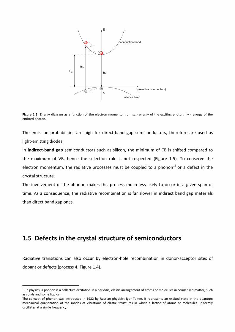
Figure 1.6 Energy diagram as a function of the electron momentum p, hν0 - energy of the exciting photon; hν - energy of the emitted photon.
The emission probabilities are high for direct-band gap semiconductors, therefore are used as
light-emitting diodes.
In indirect-band gap semiconductors such as silicon, the minimum of CB is shifted compared to
the maximum of VB, hence the selection rule is not respected (Figure 1.5). To conserve the
electron momentum, the radiative processes must be coupled to a phonon11 or a defect in the
crystal structure.
The involvement of the phonon makes this process much less likely to occur in a given span of
time. As a consequence, the radiative recombination is far slower in indirect band gap materials
than direct band gap ones.
1.5 Defects in the crystal structure of semiconductors
Radiative transitions can also occur by electron-hole recombination in donor-acceptor sites of
dopant or defects (process 4, Figure 1.4).
11
In physics, a phonon is a collective excitation in a periodic, elastic arrangement of atoms or molecules in condensed matter, such as solids and some liquids. The concept of phonon was introduced in 1932 by Russian physicist Igor Tamm, it represents an excited state in the quantum mechanical quantization of the modes of vibrations of elastic structures in which a lattice of atoms or molecules uniformly oscillates at a single frequency.
Impurities or defects can be “deep” or “shallow” centers of electron localization near the middle
of the band gap or the allowed bands. In these points electrons and holes can be considered “fixed”
compared with the electrons and holes in the conduction and valence band that transport
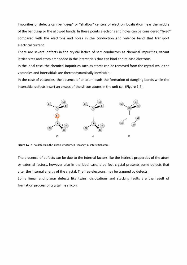
electrical current. There are several defects in the crystal lattice of semiconductors as chemical impurities, vacant
lattice sites and atom embedded in the interstitials that can bind and release electrons.
In the ideal case, the chemical impurities such as atoms can be removed from the crystal while the
vacancies and interstitials are thermodynamically inevitable.
In the case of vacancies, the absence of an atom leads the formation of dangling bonds while the
interstitial defects insert an excess of the silicon atoms in the unit cell (Figure 1.7).
Figure 1.7 A- no defects in the silicon structure, B- vacancy, C- interstitial atom.
The presence of defects can be due to the internal factors like the intrinsic properties of the atom
or external factors, however also in the ideal case, a perfect crystal presents some defects that
alter the internal energy of the crystal. The free electrons may be trapped by defects.
Some linear and planar defects like twins, dislocations and stacking faults are the result of
formation process of crystalline silicon.
1.6 Silicon nanocrystals or Silicon Quantum dots
The reduction of the semiconductor dimensions to nanoparticles with diameters of a few
nanometers leads to the world of quantum dots (QDs).
A quantum dot is a nanocrystal made of semiconductor materials, the first example was
discovered in a glass matrix by Alexey Ekimov12 at first in 1981.
The term quantum dot was coined by Mark Reed13 at Texas Instruments, to describe a form of
particle size where the excited electrons and holes are spatially confined in three dimensional
space; hence the electronic and optical properties are the result of limitations of the excitons to a
finite number of available quantum states.
In these systems the motion of the electrons, is associated to the quanto-mechanical model of a
particle in a box14, hence the electronic properties are strictly correlated with the size of the
material.
In QDs, a quantum confinement regime is reached when the size of the semiconductor nanocrystal
is below the Bohr radius and optical properties become size dependent. The Bohr radius is
characteristic of a given material and is a measure of the extension of the exciton wavefunction
over the crystal lattice.
Similar to a molecule, a quantum dot has both a quantized energy spectrum and a quantized
density of electronic states near the edge of the band gap.
Decreasing of nanocrystals size causes an increase in the band-gap energy (Figure 1.8) and
consequently variation in the electronic properties.
12
Ekimov AI, Onushchenko AA, 1981, Soviet Physics Semiconductors-USSR 16 (7): 775–778. 13
M. A. Reed, J. N. Randall, A. E. Wetsel, Phys. Rev. Lett. 60, 535, 1988. 14
Efros, A. L., Rosen, M. Annu. Rev. Mater. Sci. 2000, 30, 475–521.
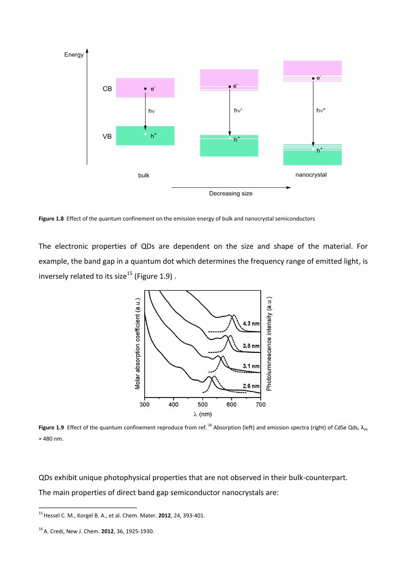
Figure 1.8 Effect of the quantum confinement on the emission energy of bulk and nanocrystal semiconductors
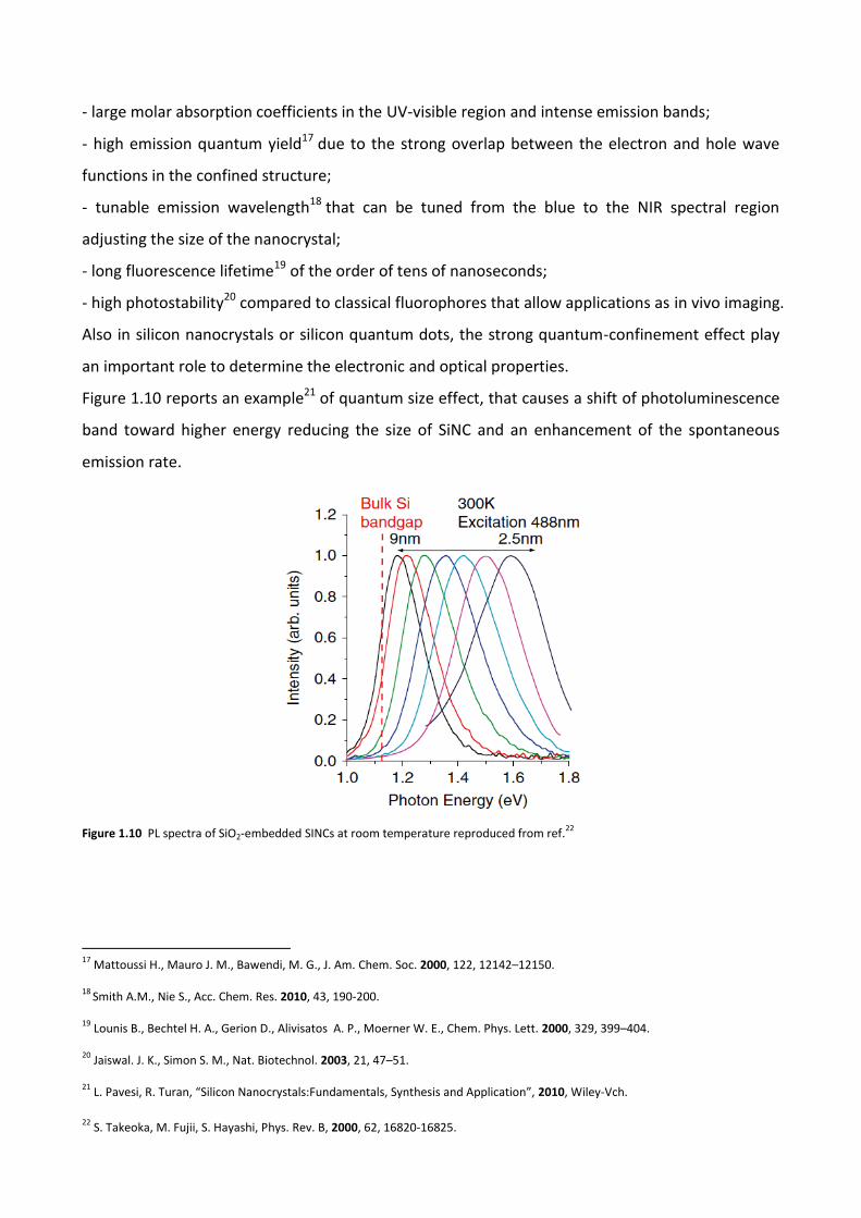
The electronic properties of QDs are dependent on the size and shape of the material. For
example, the band gap in a quantum dot which determines the frequency range of emitted light, is
inversely related to its size15 (Figure 1.9) .
Figure 1.9 Effect of the quantum confinement reproduce from ref. 16
Absorption (left) and emission spectra (right) of CdSe Qds, λex
= 480 nm.
QDs exhibit unique photophysical properties that are not observed in their bulk-counterpart.
The main properties of direct band gap semiconductor nanocrystals are:
15
Hessel C. M., Korgel B. A., et al. Chem. Mater. 2012, 24, 393-401.
16
A. Credi, New J. Chem. 2012, 36, 1925-1930.
- large molar absorption coefficients in the UV-visible region and intense emission bands;
- high emission quantum yield17 due to the strong overlap between the electron and hole wave
functions in the confined structure;
- tunable emission wavelength18 that can be tuned from the blue to the NIR spectral region
adjusting the size of the nanocrystal;
- long fluorescence lifetime19 of the order of tens of nanoseconds;
- high photostability20 compared to classical fluorophores that allow applications as in vivo imaging.
Also in silicon nanocrystals or silicon quantum dots, the strong quantum-confinement effect play
an important role to determine the electronic and optical properties.
Figure 1.10 reports an example21 of quantum size effect, that causes a shift of photoluminescence
band toward higher energy reducing the size of SiNC and an enhancement of the spontaneous
emission rate.
Figure 1.10 PL spectra of SiO2-embedded SINCs at room temperature reproduced from ref.22
17
Mattoussi H., Mauro J. M., Bawendi, M. G., J. Am. Chem. Soc. 2000, 122, 12142–12150. 18
Smith A.M., Nie S., Acc. Chem. Res. 2010, 43, 190-200. 19
Lounis B., Bechtel H. A., Gerion D., Alivisatos A. P., Moerner W. E., Chem. Phys. Lett. 2000, 329, 399–404. 20
Jaiswal. J. K., Simon S. M., Nat. Biotechnol. 2003, 21, 47–51. 21
L. Pavesi, R. Turan, “Silicon Nanocrystals:Fundamentals, Synthesis and Application”, 2010, Wiley-Vch.
22
S. Takeoka, M. Fujii, S. Hayashi, Phys. Rev. B, 2000, 62, 16820-16825.

Chapter 2
Synthetic methods
2.1 Techniques for the synthesis of silicon nanocrystals
The current knowledge of the properties of SiNCs is due to the pioneering study23 on first
luminescence nanoporous silicon (porSi) prepared by electrochemical etching of Si wafer. The
sample manifested electroluminescence and size-tunable luminescence but the great size and
shape distribution led to a complex analysis of results.
Another factor to consider in the interpretation of experiments is the enormous surface area-to-
volume ratio; for instance a compact icosahedral silicon structure with a diameter of 2.0 nm have
about 280 Si atoms24, of which 120 (43%) on the surface of the particle while a larger icosohedral
structure with 600 total Si atoms has 200 surface atoms (33%).
For that reason, the surface influences the characteristics of the material.
Computationally, it has been predicted that surface chemistry will influence the lowest
unoccupied molecular orbital energy (LUMO) and hence the optical band gap of SiNCs25.
It is evident the importance to develop methods of synthesis that allow to realize a good control of
optical properties of SiNCs by an efficient surface passivation, functionalization and size separation.
Only in this way it is possible to have a clear distinction between effects related to size, surface
and collective behavior.
Synthetic techniques for the preparation of SiNCs (Figure 2.1) can be classified according to
various parameters26:
- type of synthetic approach (top-down and bottom-up);
- nature of resulting material: SiNCs in solid state matrices and colloidal SiNCs;
18
L. T. Canham, Appl. Phys. Lett., 1990, 57, 1046-8.
24
F. Hua, M. T. Swihart, E. Ruckenstein, Langmuir, 2005, 21, 6054-6062.
25
J. Zou, R. K. Baldwin, K. A. Pettigrew, S. M. Kauzlarich, Nano Lett., 2004, 4, 1181-1186.
26
K. Dohnalovà, T. Gregorkiewicz, K. Kusovà, J. Phys., Condens. Matter, 2014, 26, 1-28.
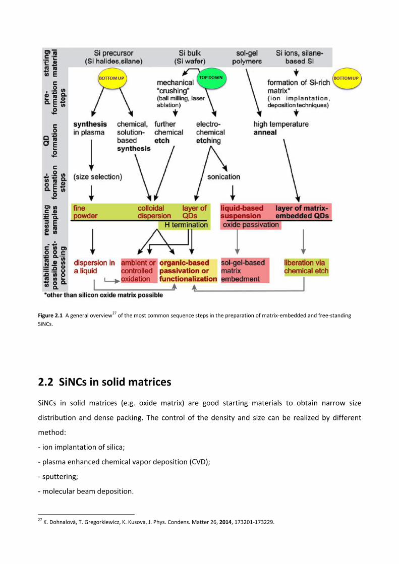
Figure 2.1 A general overview27
of the most common sequence steps in the preparation of matrix-embedded and free-standing
SiNCs.
2.2 SiNCs in solid matrices
SiNCs in solid matrices (e.g. oxide matrix) are good starting materials to obtain narrow size
distribution and dense packing. The control of the density and size can be realized by different
method:
- ion implantation of silica;
- plasma enhanced chemical vapor deposition (CVD);
- sputtering;
- molecular beam deposition.
27
K. Dohnalovà, T. Gregorkiewicz, K. Kusova, J. Phys. Condens. Matter 26, 2014, 173201-173229.
One of the major drawbacks of these techniques is low production yield and requirement of high
temperatures for the annealing step.
2.3 Colloidal SiNCs
For free-standing SiNCs we can use different synthetic approaches.
Top-down techniques as laser ablation in inert atmosphere and ball milling followed by etching
and ultrasonication.
The most common bottom-up procedures are synthesis in plasma, laser pyrolysis and chemical
solution-based synthesis.
Free-standing SiNCs are useful for a great variety of deposition processes such as drop casting, ink-
jet printing, spraying, stamping and roll-to-roll.
2.4 Production methods
Current synthetic methods are divided into three big categories: chemical, physico-chemical and
physical.
Here, the main synthetic strategies know in the literature will be presented, providing an overview
of the relationship between the method of the synthesis and SiNCs optical and chemical
properties (Table 2.1).
table 2.1
Chemical Physico-chemical Chemical solution-based synthesis Laser-induced dissociation of silane Thermal degradation in supercritical fluids
Nanosilicon from SiOx
2.5 Chemical methods
2.5.1 Chemical solution-based synthesis
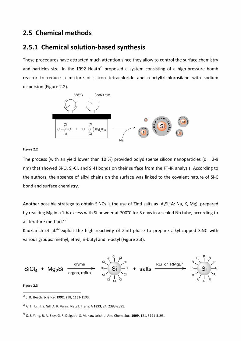
These procedures have attracted much attention since they allow to control the surface chemistry
and particles size. In the 1992 Heath28 proposed a system consisting of a high-pressure bomb
reactor to reduce a mixture of silicon tetrachloride and n-octyltrichlorosilane with sodium
dispersion (Figure 2.2).
Figure 2.2
The process (with an yield lower than 10 %) provided polydisperse silicon nanoparticles (d = 2-9
nm) that showed Si-O, Si-Cl, and Si-H bonds on their surface from the FT-IR analysis. According to
the authors, the absence of alkyl chains on the surface was linked to the covalent nature of Si-C
bond and surface chemistry.
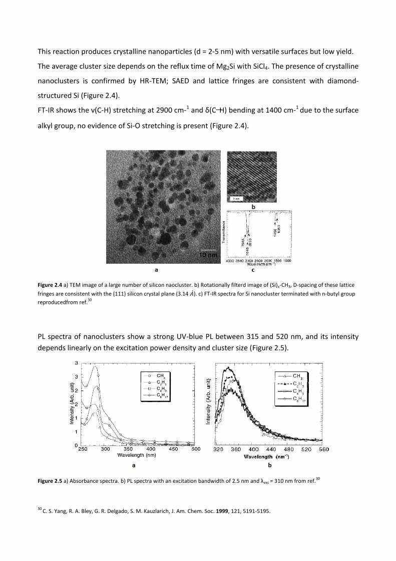
Another possible strategy to obtain SiNCs is the use of Zintl salts as (AxSi; A: Na, K, Mg), prepared
by reacting Mg in a 1 % excess with Si powder at 700°C for 3 days in a sealed Nb tube, according to
a literature method.29
Kauzlarich et al.30 exploit the high reactivity of Zintl phase to prepare alkyl-capped SiNC with
various groups: methyl, ethyl, n-butyl and n-octyl (Figure 2.3).
Figure 2.3
28
J. R. Heath, Science, 1992, 258, 1131-1133. 29
G. H. Li, H. S. Gill, A. R. Varin, Metall. Trans. A 1993, 24, 2383-2391.
30
C. S. Yang, R. A. Bley, G. R. Delgado, S. M. Kauzlarich, J. Am. Chem. Soc. 1999, 121, 5191-5195.
This reaction produces crystalline nanoparticles (d = 2-5 nm) with versatile surfaces but low yield.
The average cluster size depends on the reflux time of Mg2Si with SiCl4. The presence of crystalline
nanoclusters is confirmed by HR-TEM; SAED and lattice fringes are consistent with diamond-
structured Si (Figure 2.4).
FT-IR shows the ν(C-H) stretching at 2900 cm-1 and δ(C−H) bending at 1400 cm-1 due to the surface
alkyl group, no evidence of Si-O stretching is present (Figure 2.4).
Figure 2.4 a) TEM image of a large number of silicon naocluster. b) Rotationally filterd image of (Si)x-CH3, D-spacing of these lattice
fringes are consistent with the {111} silicon crystal plane (3.14 ). c) FT-IR spectra for Si nanocluster terminated with n-butyl group
reproducedfrom ref.30
PL spectra of nanoclusters show a strong UV-blue PL between 315 and 520 nm, and its intensity
depends linearly on the excitation power density and cluster size (Figure 2.5).
Figure 2.5 a) Absorbance spectra. b) PL spectra with an excitation bandwidth of 2.5 nm and λexc = 310 nm from ref.
30
30 C. S. Yang, R. A. Bley, G. R. Delgado, S. M. Kauzlarich, J. Am. Chem. Soc. 1999, 121, 5191-5195.

In other contribution31, alkyl capped SiNCs have been prepared via oxidation of magnesium silicide
with bromine (Figure 2.6) and subsequent coverage of the surface with alkyl-lithium reagent.
Figure 2.6
HR-TEM confirms the crystalline nature of nanoparticles with an average diameter of 4.5 nm. The
control over the size is possible varying the silicon:bromine ratio. Fluorescence spectroscopy
indicates an ultraviolet-blue photoluminescence (Figure 2.7) which is attributed to both quantum
confinement and surface termination.
Figure 2.7 a) UV-visible spectra of silicon nanoparticles b) PL spectra reproduced from ref.31
31
K. A. Pettigrew, Q. Liu, P. P. Power, S. Kauzlarich, Chem. Mater., 2003, 15, 4005-4011.
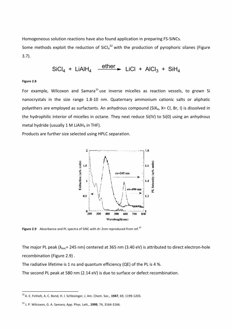
Homogeneous solution reactions have also found application in preparing FS-SiNCs.
Some methods exploit the reduction of SiCl432 with the production of pyrophoric silanes (Figure
3.7).
Figure 2.8
For example, Wilcoxon and Samara33 use inverse micelles as reaction vessels, to grown Si
nanocrystals in the size range 1.8-10 nm. Quaternary ammonium cationic salts or aliphatic
polyethers are employed as surfactants. An anhydrous compound (SiX4, X= Cl, Br, I) is dissolved in
the hydrophilic interior of micelles in octane. They next reduce Si(IV) to Si(0) using an anhydrous
metal hydride (usually 1 M LiAlH4 in THF).
Products are further size selected using HPLC separation.
Figure 2.9 Absorbance and PL spectra of SiNC with d= 2nm reproduced from ref.
33
The major PL peak (λexc= 245 nm) centered at 365 nm (3.40 eV) is attributed to direct electron-hole
recombination (Figure 2.9) .
The radiative lifetime is 1 ns and quantum efficiency (QE) of the PL is 4 %.
The second PL peak at 580 nm (2.14 eV) is due to surface or defect recombination.
32
A. E. Finholt, A. C. Bond, H. I. Schlesinger, J. Am. Chem. Soc., 1947, 69, 1199-1203. 33
J. P. Wilcoxon, G. A. Samara, App. Phys. Lett., 1999, 74, 3164-3166.

Tilley at al.34 later reported a variation of this method to obtain hydrophilic or hydrophobic silicon
nanocrystals with good monodispersion (1-2 nm). Tetraoctylammonium bromide is used as the
surfactant and the hydride reducing agent produces hydrogen-terminated particle surfaces. The
SiNCs are capped with either allylamine or 1-heptene (Figure 2.10) by platinic-acid catalyzed-
hydrosilylation.
Figure 2.10 Scheme of the synthesis
Optical characterization is performed on colloidal solutions with two types of surface-capped
SiNCs with identical size distribution. Allylamine-SiNC shows an absorption profile with a greater
spectral range than 1-heptene-SiNCs (Figure 2.11); in addition there is a shoulder at 340 nm that
can be due to the direct band gap transition.
Figure 2.11 Absorption of a) 1-heptene-SiNCs, b) allylamine-SiNCs reproduced from ref.34
34
J. H. Warner, H. Rubinsztein, R. D. Tilley, J. Phys. Chem. B, 2005, 109, 19064-19067.
From the analysis of PL properties (Figure 2.12) there are two differences:
- allylamine-SINCs exhibit a major red shif in the PL peak position than 1-heptene SiNCs;
- 1-heptene-SiNCs display emission with higher energy than the allylamine-SiNC for the same
excitation wavelength.
Figure 2.12 PL spectra of a) allylamine-SiNCs, b) 1-heptene-SiNCs
These results demonstrate the effect of the ligand on the SiNCs optical properties and its role in
the radiative recombination mechanisms.
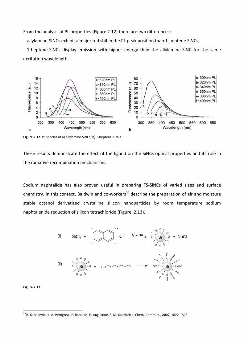
Sodium naphtalide has also proven useful in preparing FS-SiNCs of varied sizes and surface
chemistry. In this context, Baldwin and co-workers35 describe the preparation of air and moisture
stable octanol derivatized crystalline silicon nanoparticles by room temperature sodium
naphtalenide reduction of silicon tetrachloride (Figure 2.13).
Figure 2.13
35
R. K. Baldwin, K. A. Pettigrew, E. Ratai, M. P. Augustine, S. M. Kauzlarich, Chem. Commun., 2002, 1822-1823.
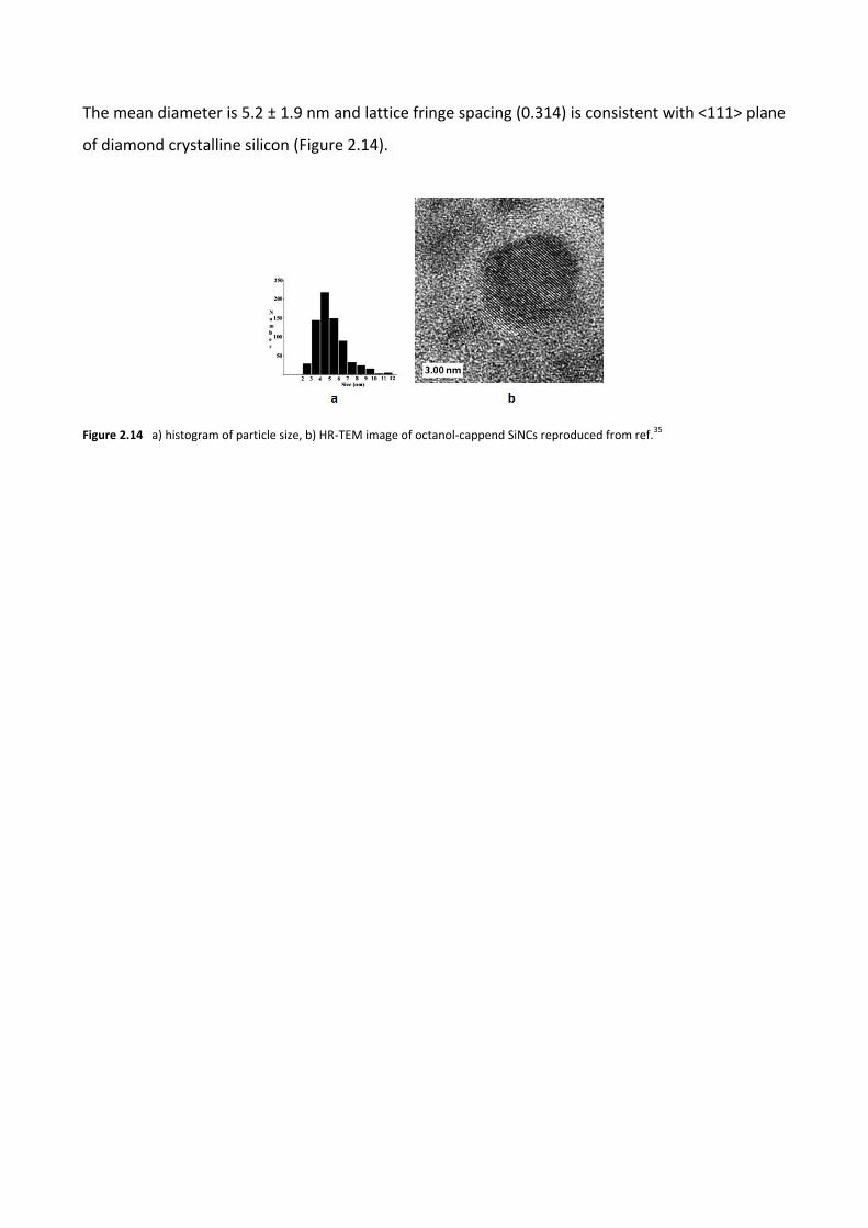
The mean diameter is 5.2 ± 1.9 nm and lattice fringe spacing (0.314) is consistent with ˂111˃ plane
of diamond crystalline silicon (Figure 2.14).
Figure 2.14 a) histogram of particle size, b) HR-TEM image of octanol-cappend SiNCs reproduced from ref.
35

2.5.2 Thermal degradation in supercritical fluids
Precursor thermal decomposition is an attractive method for preparing semiconductors
nanoparticles. In 2001, Korgel and coworkers36 have developed a method to produce highly
crystalline, organic-monolayer passivated SiNCs by thermal degradation of diphenylsilane (Si
precursor) in supercritical solvent mixtures of octanol and hexane (Figure 2.15).
Figure 2.15
The high temperature is necessary to induce Si crystallization.
The advantage of a supercritical solvent is the high diffusion coefficient, on the order of 10-3 to 10-4
cm2 s-1, that enables the rapid reactant diffusion necessary to achieve diffusion-limited growth for
the narrowest particle size distributions.
Relatively size-monodisperse SiNCs, with a diameter range from 15 to 40 Å are obtained with
yields 0.5 – 5 %, they show a crystalline core with a lattice spacing of 3.1 Å, consistent with the
(111) separation in the Si diamond-like structure (Figure 2.16).
Figure 2.16 HR-TEM image of a 40 Å diameter SiNC reproduce from ref.36
36
J. D. Holmes, K. J. Ziegler, R. C. Doty, L. E. Pell, K. P. Johnston, B. A. Korgel, J. Am. Chem. Soc. 2001, 123, 3743-3748.

Control over the particles size is realized through systematic variation of the octanol: Si ratio.
Silicon nanocrystals exhibit a significant blue shift in optical properties from the bulk band gap
energy of 1.2 eV due to quantum confinement effects.
As shown in Figure 2.17, the smaller SiNCs emit in the UV region and the larger exhibit a green PL
with quantum yields of 20 % at room temperature.
Figure 2.17 Absorbance (solid lines) and PL spectra of SiNCs at room temperature reproduced from ref.31
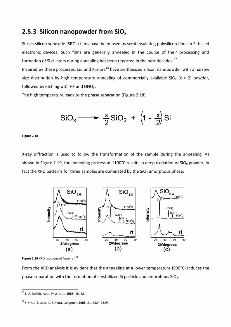
2.5.3 Silicon nanopowder from SiOx
Si-rich silicon suboxide (SROs) films have been used as semi-insulating polysilicon films in Si-based
electronic devices. Such films are generally annealed in the course of their processing and
formation of Si clusters during annealing has been reported in the past decades.37
Inspired by these processes, Liu and Kimura38 have synthesized silicon nanopowder with a narrow
size distribution by high temperature annealing of commercially available SiOx (x < 2) powder,
followed by etching with HF and HNO3.
The high temperature leads to the phase separation (Figure 2.18).
Figure 2.18
X-ray diffraction is used to follow the transformation of the sample during the annealing. As
shown in Figure 2.19, the annealing process at 1100°C results in deep oxidation of SiOx powder, in
fact the XRD patterns for three samples are dominated by the SiO2 amorphous phase.
Figure 2.19 XRD reproduced from ref.38
From the XRD analysis it is evident that the annealing at a lower temperature (900°C) induces the
phase separation with the formation of crystallized Si particle and amorphous SiO2.
37
L. A. Nesbit, Appl. Phys. Lett, 1985, 46, 38.
38
S-M Liu, S. Sato, K. Kimura, Langmuir, 2005, 21, 6324-6329.

Also the effect of HF etching process is studied by XRD (Figure 2.20).
Figure 2.20 The change of XRD patterns during HF etching process. Curves a and b were measured on SiO1.6 starting material and 900 °C annealed sample, respectively. Curves c-g were obtained after etching for (c) 1 h, (d) 2 h, (e) 3 h, (f) 4 h, and (g) 6 h reproduced from ref.
38
From pattern a → g, the oxide phase (wide diffraction peak at 2θ of 21°) decrease with the etching
time and disappears after 6 hours. The formation of Si nanoparticles is confirmed by HR-TEM, the
average size of particle is 4.2 nm with polydispersity of 12 %.
Freshly etched sample shows two emission bands at 520 nm and 397 nm (Figure 2.21).
Figure 2.21 (a) PL spectra of sample after HF etching for (I) 3 h, (II) 6 h, and (III) 1 day recorded by excitation at 355 nm wavelength; (b) PLE spectra recorded at detection wavelength of (I) 520 nm, (II) 502 nm, (III) 487 nm, and (IV) 400 nm. Spectra I and IV were recorded on sample after HF etching for 3 h, spectra II and III were recorded on sample after HF etching for 6 h and 1 day, respectively. Reproduced from ref.
38
After 1 day, the PL band at 520 nm blue-shifts to 487 nm while the high energy emission stays at
397 nm. The emission band at 520 nm is ascribed to the radiative recombination of electron-hole
pairs. These results are consistent with the PL bands observed by Korgel39 and Kauzlarich40 from
organic-passivated SiNCs with an average size of 2-5 nm.
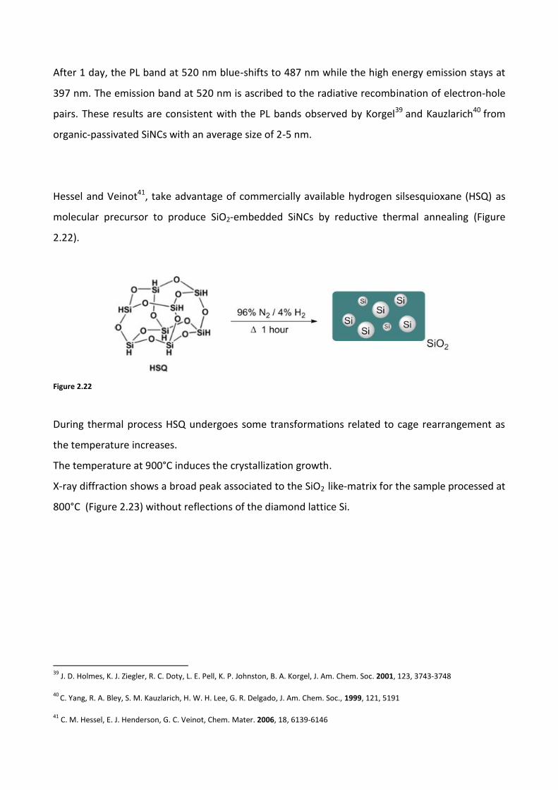
Hessel and Veinot41, take advantage of commercially available hydrogen silsesquioxane (HSQ) as
molecular precursor to produce SiO2-embedded SiNCs by reductive thermal annealing (Figure
2.22).
Figure 2.22
During thermal process HSQ undergoes some transformations related to cage rearrangement as
the temperature increases.
The temperature at 900°C induces the crystallization growth.
X-ray diffraction shows a broad peak associated to the SiO2 like-matrix for the sample processed at
800°C (Figure 2.23) without reflections of the diamond lattice Si.
39
J. D. Holmes, K. J. Ziegler, R. C. Doty, L. E. Pell, K. P. Johnston, B. A. Korgel, J. Am. Chem. Soc. 2001, 123, 3743-3748
40
C. Yang, R. A. Bley, S. M. Kauzlarich, H. W. H. Lee, G. R. Delgado, J. Am. Chem. Soc., 1999, 121, 5191
41
C. M. Hessel, E. J. Henderson, G. C. Veinot, Chem. Mater. 2006, 18, 6139-6146
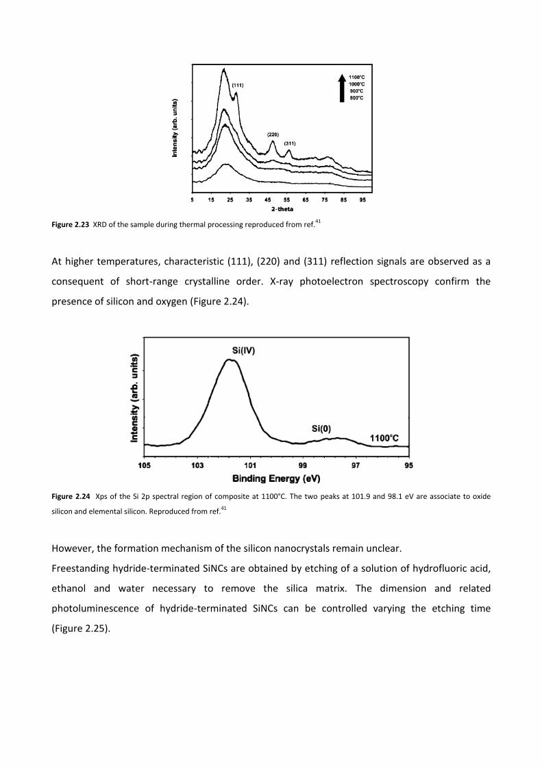
Figure 2.23 XRD of the sample during thermal processing reproduced from ref.41
At higher temperatures, characteristic (111), (220) and (311) reflection signals are observed as a
consequent of short-range crystalline order. X-ray photoelectron spectroscopy confirm the
presence of silicon and oxygen (Figure 2.24).
Figure 2.24 Xps of the Si 2p spectral region of composite at 1100°C. The two peaks at 101.9 and 98.1 eV are associate to oxide
silicon and elemental silicon. Reproduced from ref.41
However, the formation mechanism of the silicon nanocrystals remain unclear.
Freestanding hydride-terminated SiNCs are obtained by etching of a solution of hydrofluoric acid,
ethanol and water necessary to remove the silica matrix. The dimension and related
photoluminescence of hydride-terminated SiNCs can be controlled varying the etching time
(Figure 2.25).
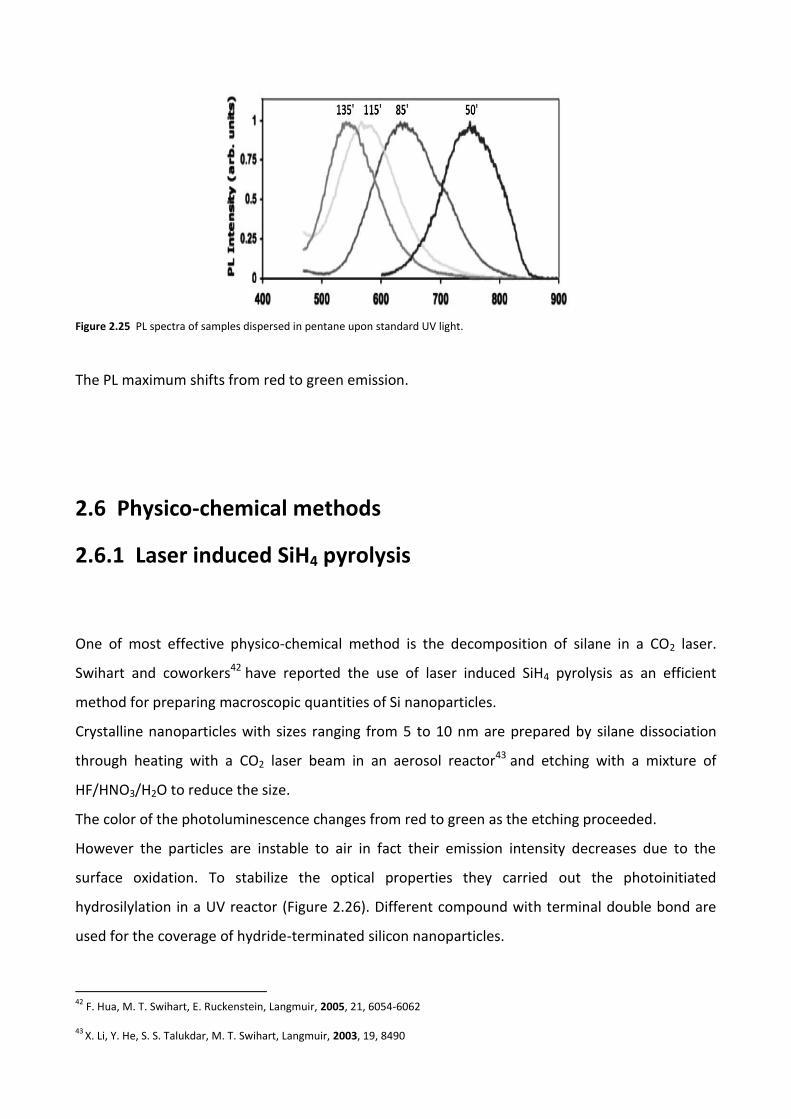
Figure 2.25 PL spectra of samples dispersed in pentane upon standard UV light.
The PL maximum shifts from red to green emission.
2.6 Physico-chemical methods
2.6.1 Laser induced SiH4 pyrolysis
One of most effective physico-chemical method is the decomposition of silane in a CO2 laser.
Swihart and coworkers42 have reported the use of laser induced SiH4 pyrolysis as an efficient
method for preparing macroscopic quantities of Si nanoparticles.
Crystalline nanoparticles with sizes ranging from 5 to 10 nm are prepared by silane dissociation
through heating with a CO2 laser beam in an aerosol reactor43 and etching with a mixture of
HF/HNO3/H2O to reduce the size.
The color of the photoluminescence changes from red to green as the etching proceeded.
However the particles are instable to air in fact their emission intensity decreases due to the
surface oxidation. To stabilize the optical properties they carried out the photoinitiated
hydrosilylation in a UV reactor (Figure 2.26). Different compound with terminal double bond are
used for the coverage of hydride-terminated silicon nanoparticles.
42
F. Hua, M. T. Swihart, E. Ruckenstein, Langmuir, 2005, 21, 6054-6062 43
X. Li, Y. He, S. S. Talukdar, M. T. Swihart, Langmuir, 2003, 19, 8490
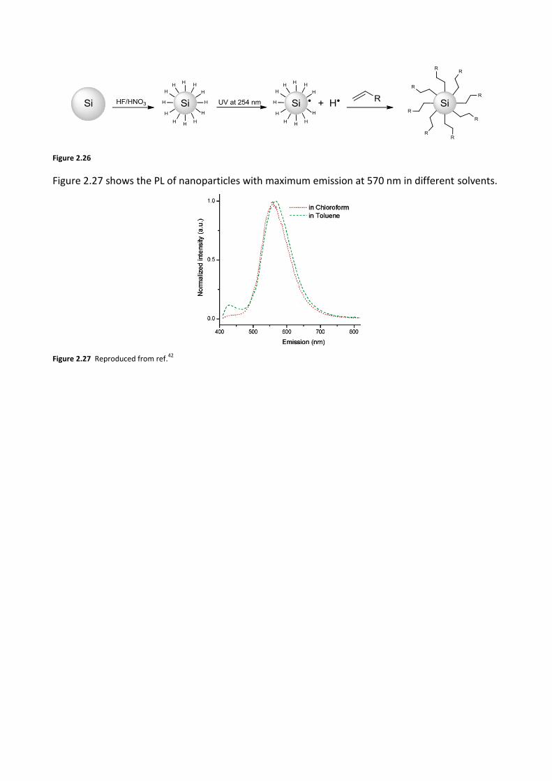
Figure 2.26
Figure 2.27 shows the PL of nanoparticles with maximum emission at 570 nm in different solvents.
Figure 2.27 Reproduced from ref.42
Chapter 3
Techniques for the characterization of
silicon nanocrystals
3.1 Introduction
The small size and complex surface chemistry of SiNCs require the use of different analytical
techniques such as X-ray diffractometry (XRD), Fourier transform infrared spectroscopy (FTIR), X-
ray photoelectron spectroscopy (XPS), nuclear magnetic resonance spectroscopy (NMR),
transmission electron microscopy (TEM), and photoluminescent spectroscopy (PL).
This set of techniques offer a concrete characterization of SiNCs in order to have a good
understanding of their properties.
3.2 X-ray diffraction (XRD)
XRD data were obtained with Si nanocrystals (5 mg) on quartz substrates using a Bruker-Nonius D8
Advance diffractometer. Scans of 2θ° were performed from 10–90° in 0.02 (2θ°) increments at a
scan rate of 12.0° min− 1 for 6 h.
XRD data for freshly etched Si nanocrystals were collected immediately after removing the
nanocrystals from the etching solution to minimize oxidation of the nanocrystals prior to the
measurement.

3.3 ATR-FTIR spectroscopy
ATR-FTIR spectra (400–4000 cm− 1) were acquired using a Thermo Mattson Infinity Gold FTIR with
an ATR (attenuated total reflectance) stage. Samples were prepared by drop casting from
chloroform dispersions after a 20 min ambient clean up in glass centrifuge tubes
3.4 X-ray photoelectronspectroscopy (XPS)
XPS was performed on a Kratos photoelectron spectrometer equipped with a charge neutralizer
and 180° hemispherical electron energy analyzer. XPS samples were prepared by dropcasting Si
nanocrystals (≈ 5 mg) onto indium tin oxide- (ITO) coated glass substrates and degassed at 10−7
Torr for 1 day prior to analysis. XPS data were internally standardized with respect to the O 1s
peak position (530 eV).
3.5 Nuclear magnetic resonance analysis (NMR)
1H-NMR and 13C-NMR spectra were recorded on Varian INOVA 400 (400 MHz) spectrometers.
Chemical shifts are reported in ppm using tetramethylsilane as the internal reference standard.
Data are reported as follows: chemical shift, multiplicity (s = singlet, d = doublet, t = triplet, q =
quartet, br = broad, m = multiplet), coupling constants (Hz). LC-electrospray ionization mass
spectra were obtained with an Agilent Technologies MSD1100 single-quadrupole mass
spectrometer. Chromatographic purification was performed on 240-400 mesh silica gel. All
reactions were carried out under a nitrogen atmosphere in flame-dried glassware using standard
inert techniques for introducing reagents and solvents.

3.6 Transmission electron microscopy (TEM)
TEM imaging was performed on a FEI Tecnai Biotwin TEM operated at 80 kV accelerating voltage.
TEM samples were made by drop casting toluene dispersions onto carbon-coated 200 mesh
copper TEM grids (Electron Microscopy Science).
3.7 Photophysical Techniques
Absorption measurements
UV-visible absorbance spectra reported in Chapter 4 and 5, were recorded with a Perkin Elmer λ40
spectrophotometer (Figure 3.1) in the 190-1100 nm range at room temperature, using quartz cells
with 1.0 cm and 5.0 cm path length Hellma®.
The precision on the wavelength values was ± 2 nm. Molar absorption coefficient values were
determined using the Lambert–Beer law; the experimental error, mostly due to weighting error,
can be estimated to be around ± 5%.
Figure 3.1 Schematic view of standard double-beam spectrophotometer.
Luminescence measurements

When necessary, solutions were deaerated by freeze-pump-thaw cycles. Emission spectra and
excitation spectra in the range 250-900 nm, were obtained with a Perkin Elmer LS-50
spectrofluorometer, equipped with a Hamamatsu R928 phototube (Figure 3.2), or an Edinburgh
FLS920 spectrofluorometer equipped with a Ge-detector for emission in the NIR spectral region.
Correction of the emission spectra for detector sensitivity in the 650-900 nm spectral region was
performed.44
Figure 3.2 Schematic view of standard spectrofluorimeter.
Luminescence quantum yield measurements
Luminescence quantum yields were determined on solution samples at room temperature
referring to the relative method optimized by Demas and Crosby.45
The quantum yield is expressed as:
S =R (As/AR)(nS/nR)2
44
The Exploration of Supramolecular Systems and Nanostructures by Photochemical Techniques, P. Ceroni Ed., Springer, Lecture
Notes in Chemistry, Vol. 78, Heidelberg, Germany, 2012. 45
Demas J. N., Crosby G. A., J. Phys. Chem. 1971, 75, 991-1024.

Where , A, n indicate the luminescence quantum yield, the area subtended by the emission
band (in the intensity versus frequency spectrum) and the refractive index of the solvent used for
the preparation of the solution, respectively; the subscripts S and R stand for sample and
reference, respectively.
AS and AR must be obtained using the appropriate luminescence standard and under the same
instrumental conditions; furthermore the sample and the reference must exhibit the same
absorption at the excitation wavelength. Different standards were selected depending on the
spectral region of interest.
In the Chapter 4, standard used are: naphthalene in deaerated cyclohexane solution,46 quinine
sulfate in H2SO4 0.5 M, 1,1',3,3,3',3'-hexamethylindotricarbocyanine iodide (HITCI) in ethanol.47,48
In the Chapter 5, the standard used are: [Ru(bpy)3]Cl2 in air-equilibrated water ΦPL=0.040,49
1,1',3,3,3',3'-hexamethylindotricarbocyanine iodide (HITCI) in air-equilibrated ethanol ΦPL=0.30).50
Luminescence lifetime measurements
PL lifetime measurements in the range 0.5 ns to 1 μs were performed by an Edinburgh FLS920
spectrofluorometer equipped with a TCC900 card for data acquisition in time-correlated single-
photon counting experiments (0.2 ns time resolution) with a 340 nm pulsed diode and a LDH-P-C-
405 pulsed diode laser. PL lifetime measurements in the range 10 μs to 1 s were performed on a
Perkin Elmer LS-50 spectrofluorometer equipped with a pulsed Xe lamp. The estimated
experimental errors is 5%.
46
Montalti M., Credi A., Prodi L., Gandolfi M. T., Handbook of Photochemistry, ed. Taylor & Francis, London, 3rd edn., 2006, ch. 10. 47
Würth C., Pauli J., Lochmann C., Spieles M., Resch-Genger U., Anal. Chem. 2012, 84, 1345-1352. 48
Würth C., Grabolle M., Pauli J., Spieles M., Resch-Genger U., Nature Prot. 2013, 8, 1535-1550.
49
K. Suzuki, A. Kobayashi, S. Kaneko, K. Takehira, T. Yoshihara, H. Ishida, Y. Shiina, S. Oishi, S. Tobita, Phys. Chem. Chem. Phys. 2009, 11, 9850.
50
C. Würth, M. Grabolle, J. Pauli, M. Spieles, U. Resch-Genger, Nat. Protoc. 2013, 8, 1535.

Laser flash-photolysis experiments
The experiments of ns-transient absorption spectroscopy on Silicon nanocrystals were performed
by an Ultrafast Systems apparatus equipped with a Hamamatsu R928 phototube connected to a
Tektronix TDS380 (400 MHz) oscilloscope and a Continuum Surelite I-10 Nd:YAG laser source (λex =
532 nm).
Chapter 4
Silicon nanocrystals functionalized with
pyrene units: efficient light-harvesting
antennae with bright near-infrared emission
4.1 Introduction
Silicon nanocrystals exhibit interesting optical and electronic properties related to the quantum
confinement effect. They can be efficient light emitters, with emission wavelength that can be
tuned by size from the near-infrared (NIR) into the visible range.51
The indirect bandgap of Si, however, still makes light absorption relatively weak compared to
quantum dots of direct band gap semiconductors, especially at wavelengths near the absorption
edge.52
To circumvent this drawback, we exploited the covalent functionalization of SiNCs surface with a
ligand (pyrene) capable of strong light absorption and efficient energy transfer to the SiNCs.
The aim of this work is to increase the optical absorption of SiNCs by molecular antennae while
retaining their emission properties.
Two families of SiNCs with different average diameters 3.0 and 5.0 nm have been studied.
4.2 Synthesis of oxide-embedded silicon nanocrystals of
different sizes
Silicon nanocrystals were synthesized by the method developed by Hessel et al.53 The process use
hydrogen silsesquioxane (HSQ) as precursor. This compound belongs to the silsesquioxane family, 51
Brus L. E., Szajowski P. F., Wilson W. L., Harris T. D., Schuppler S., Citrin P. H., J. Am. Chem. Soc. 1995, 117, 2915−2922.
52 Hessel C. M., Reid D., Panthani M. G., Rasch M. R., Goodfellow B. W., Wei J., Fujii H., Akhavan V., Korgel B. A., Chem. Mater. 2012, 24, 393−401.

a class of molecules composed of silicon-oxygen framework with empirical formula (RSiO1.5)
where R = hydrogen, alkyl, silyl and aromatic.
HSQ (H8Si8O12) has been investigated as model silica surface, 54 catalytical support 55 and
luminescent material.56
In a typical synthesis, 40 mL of Fox-16 (purchased from Dow Corning, 16wt% hydrogen
silsesquioxane (HSQ) in isobutyl methyl ketone and toluene) is dried under vacuum on a schlenk
line for 6 hours. The resulting white solid is placed in a quartz crucible and transferred to a tube
furnace (Figure 4.1).
Figure 4.1 Steps for the tube furnance.
After purging with forming gas (93% N2, 7% H2), the tube furnace is heated to 1100oC (2.6 nm
diameter) or 1200oC (5.0 nm diameter) at a heating rate of 18oC/min and then held at that
temperature for an hour.
The accepted stages57 of HSQ thermal processing are summarized in (Figure 4.2) and are
attributed to:
53
Hessel C. M., Henderson E. J., Veinot J. G. C., Chem. Mater. 2006, 18, 6139-6146. 54
Feher F. J., Budzichowski T. A., Blanski R. L., Weller K. J., Ziller J. W., Organometallics 1991, 10, 2526. 55
Tour, J. M.; Pendalwar, S. L.; Cooper, J. P. Chem. Mater. 1990, 2, 647.
56
Azinovic D., Cai J., Eggs C., Konig H., Marsmann H. C., Veprek S. J. Lumin. 2002, 97, 40.
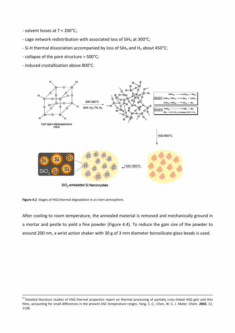
- solvent losses at T < 200°C;
- cage network redistribution with associated loss of SiH4 at 300°C;
- Si-H thermal dissociation accompanied by loss of SiH4 and H2 about 450°C;
- collapse of the pore structure ˃ 500°C;
- induced crystallization above 800°C.
Figure 4.2 Stages of HSQ thermal degradation in an inert atmosphere.
After cooling to room temperature, the annealed material is removed and mechanically ground in
a mortar and pestle to yield a fine powder (Figure 4.4). To reduce the gain size of the powder to
around 200 nm, a wrist action shaker with 30 g of 3 mm diameter borosilicate glass beads is used.
57
Detailed literature studies of HSQ thermal properties report on thermal processing of partially cross-linked HSQ gels and thin films, accounting for small differences in the present DSC temperature ranges. Yang, C.-C.; Chen, W.-C. J. Mater. Chem. 2002, 12, 1138.

Figure 4.4
The final sample has been characterized with different techniques.
4.2.1 Material characterization
X-ray diffraction
The crystallization of matrix-embedded SiNCs was confirmed by X-ray power diffraction. When the
sample is thermally processed at 1100°C, (220), (311), (111) reflection peaks increase in intensity
and narrow. The position and intensities of these peaks (Figure 4.3) are consistent with diamond
lattice Si.

Figure 4.3 X-ray power diffraction of SiO2/SiNCs at different temperatures.46
ATR-FTIR spectroscopy
ATR-FTIR spectroscopy (Figure 4.5) shows a characteristic strong absorption at 1090 cm-1 assigned
to ν(Si−O) stretching due to the SiO2 matrix and ν(Si−O-Si) stretching at 1048 cm-1 related to the
interactions at the interface SiO2/SiNCs.
The presence of Si-H bond is evidenced by weak ν(Si−H) stretching at 2035 cm-1 and δ(Si−H)
bending at 800 cm-1.
Figure 4.5 ATR-FTIR spectra of oxide-embedded SiNCs.

X-ray photoelectron spectroscopy
XPS of the oxide-embedded nanocrystals (Figure 4.6) exhibits peaks of elemental Si and SiO2 at
99.4 eV and 103.5 eV respectively.58 There is minimal suboxide (Si+1 and Si+2) present, indicating
that there is an abrupt interface between silicon nanocrystals and the SiO2 matrix.59
Figure 4.6 XPS of oxide-embedded SiNCs reproduced from ref.51
Optical properties
Figure 4.7 shows the photoluminescence spectra of SiO2/SiNCs. Under excitation with the 325 nm
line of He-Cd laser, emission at 800 nm from solid film is observed.60
58
C. M. Hessel, E. J. Henderson, J. G. C. Veinot, J. Phys. Chem. C 2007, 111, 6956. 59
D. A. Luh, T. Miller, T. C. Chiang, Phys. Rev. Lett. 1997, 79, 3014.
60
Hessel C. M., Henderson E. J., Veinot J. G. C., Chem. Mater. 2006, 18, 6139-6146.

Figure 4.7 Photoluminescence spectrum from a pentane suspension of the finely ground powder from annealing at 1100°C,
reproduced from ref.53
4.3 Liberation of hydride-terminated-SiNCs from silica matrix
The Si nanocrystals are liberated from the SiO2 matrix by etching with a solution of 48% HF and
37.5% HCl (10:1 v/v) in the dark for 4-6 hours (Figure 4.8). During the oxide removal process the
solution progresses from a dark brown to light yellow color as the nanocrystal size decrease.
Figure 4.8
HF etches both Si and SiO2, but the SiO2-etching is much faster due to the polarity difference
between Si-Si and Si-O bonds.61 Hydride-terminated SiNCs are isolated as wet powder by
centrifugation and rinsed once with deionized (DI) water, twice with ethanol, and once with
chloroform.
To monitor changes in the surface chemistry after chemical treatment, freshly HF-etched sample
has been characterized with XPS and PL spectroscopy (Figure 4.9). After HF etching, there is only a
61
K. R. William, K. Gupta, M. Wasilik, J. Microelectromech. Syst. 2003, 12, 761.

single XPS peak at 99.2 eV (Figure 4.9 a) associated to elemental Si, proving the removal of the
entire matrix.62
(Figure 4.9 b) shows the optical properties of SiNCs before and after HF-etching. The as-prepared
oxide-embedded Si nanocrystals exhibit a PL peak at 780 nm. HF etching shifts the PL to lower
wavelength (600 nm).
Figure 4.9 a) XPS of oxide embedded SiNCs before and after HF-etching, b) room temperature PL emission (dotted line), PLE (solid
line) and UV-Vis absorbance spectra (dashed line) of SiNCs dispersed in CHCl3 before and after etching with λexc = 320. Reproduce
from ref.55
62
C. M. Hessel, M. R. Rasch, J. L. Hueso, B. W. Goodfellow, V. A. Akhavan, J. W. Tunnel, B. A. Korgel, Small 2010, 18, 2026-2034.
4.4 Covalent functionalization of SiNCs with pyrene units
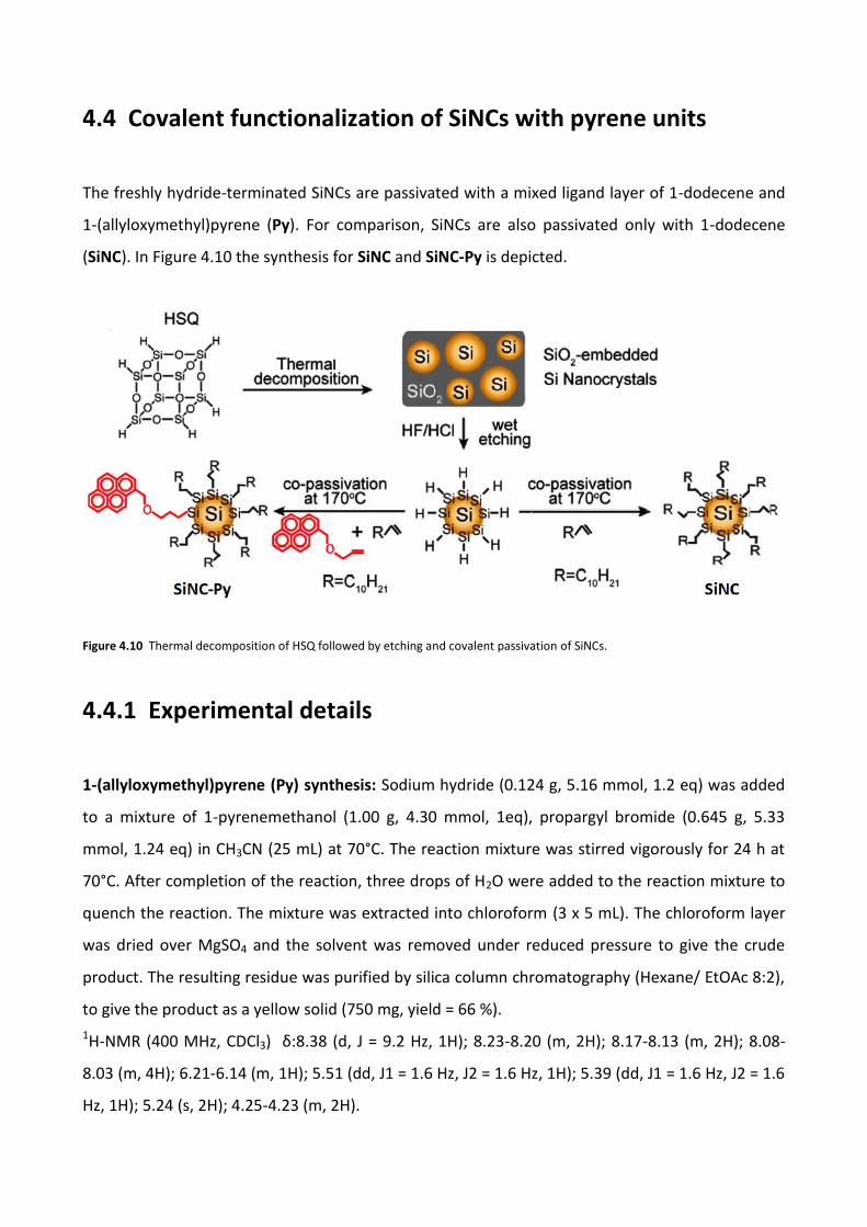
The freshly hydride-terminated SiNCs are passivated with a mixed ligand layer of 1-dodecene and
1-(allyloxymethyl)pyrene (Py). For comparison, SiNCs are also passivated only with 1-dodecene
(SiNC). In Figure 4.10 the synthesis for SiNC and SiNC-Py is depicted.
Figure 4.10 Thermal decomposition of HSQ followed by etching and covalent passivation of SiNCs.
4.4.1 Experimental details
1-(allyloxymethyl)pyrene (Py) synthesis: Sodium hydride (0.124 g, 5.16 mmol, 1.2 eq) was added
to a mixture of 1-pyrenemethanol (1.00 g, 4.30 mmol, 1eq), propargyl bromide (0.645 g, 5.33
mmol, 1.24 eq) in CH3CN (25 mL) at 70°C. The reaction mixture was stirred vigorously for 24 h at
70°C. After completion of the reaction, three drops of H2O were added to the reaction mixture to
quench the reaction. The mixture was extracted into chloroform (3 x 5 mL). The chloroform layer
was dried over MgSO4 and the solvent was removed under reduced pressure to give the crude
product. The resulting residue was purified by silica column chromatography (Hexane/ EtOAc 8:2),
to give the product as a yellow solid (750 mg, yield = 66 %).
1H-NMR (400 MHz, CDCl3) δ:8.38 (d, J = 9.2 Hz, 1H); 8.23-8.20 (m, 2H); 8.17-8.13 (m, 2H); 8.08-
8.03 (m, 4H); 6.21-6.14 (m, 1H); 5.51 (dd, J1 = 1.6 Hz, J2 = 1.6 Hz, 1H); 5.39 (dd, J1 = 1.6 Hz, J2 = 1.6
Hz, 1H); 5.24 (s, 2H); 4.25-4.23 (m, 2H).

13C-NMR (100 MHz, CDCl3) δ:134.9, 131.4; 131.3; 131.2; 130.8; 129.2; 127.6; 127.4; 127.3; 126.8;
125.8; 125.2; 125.1; 124.9; 124.7; 124.5; 123.3; 117.3; 71.2, 70.6.ESI-MS : 232 [M- C3H5]+
SiNC and SiNC-Py Synthesis: The nanocrystals are dispersed in either 5 mL of 1-dodecene, or 5 mL
of 1-dodecene with 165 mg of 1-(allyloxymethyl)pyrene (1:36 pyrene:dodecene molar ratio) or
490 mg of 1-(allyloxymethyl)pyrene (1:12 pyrene:dodecene molar ratio). The initially turbid
dispersions are put through three freeze-pump-thaw cycles, and then heated to 170°C under N2
flow for 12 hours. Over time, the dispersions become optically clear, indicating that passivation of
Si nanocrystals has occurred. The nanocrystals are then purified by transfer to a glass centrifuge
tube and centrifugation at 8000 rpm for 5 min. Poorly-capped nanocrystals precipitate from the
mixture and are discarded. The supernatant is transferred to another glass centrifuge tube and
washed with four consecutive centrifugation/precipitation cycles using toluene/ethanol
solvent/antisolvent pair. The final SiNC and SiNC-Py samples were dispersed in toluene at a
concentration of 5 mg/mL until further characterization
NMR spectral characterization
Covalent pyrene functionalization of the SiNC-Py is confirmed by 1H and 13C NMR spectroscopy.
Figures 4.11-4.14 show 1H and 13C NMR spectra of Py, SiNC, and SiNC-Py. 1H NMR spectra of SiNC
and SiNC-Py (Figure 4.13) with an average diameter of 3.0 nm (Py:dodecene ratio of 1:36 used in
the passivation) dispersed in CDCl3 at room temperature provide evidence of a covalently linked
surface layer. The 1H NMR spectra of SiNC show a uniform chemical environment for the alkyl
chains with a single methyl resonance and several distinct methylene resonances. The 1H NMR
spectrum of SiNC-Py shows additional signals compared to SiNC attributable to pyrene moieties.
The molar ratio of pyrene appended groups and dodecene alkyl chains on the Si nanocrystals
determined by integration of the relevant resonances in the 1H NMR spectra was 1:20, which is
close to the Py:dodecene molar ratio (1:36) used in the passivation step.
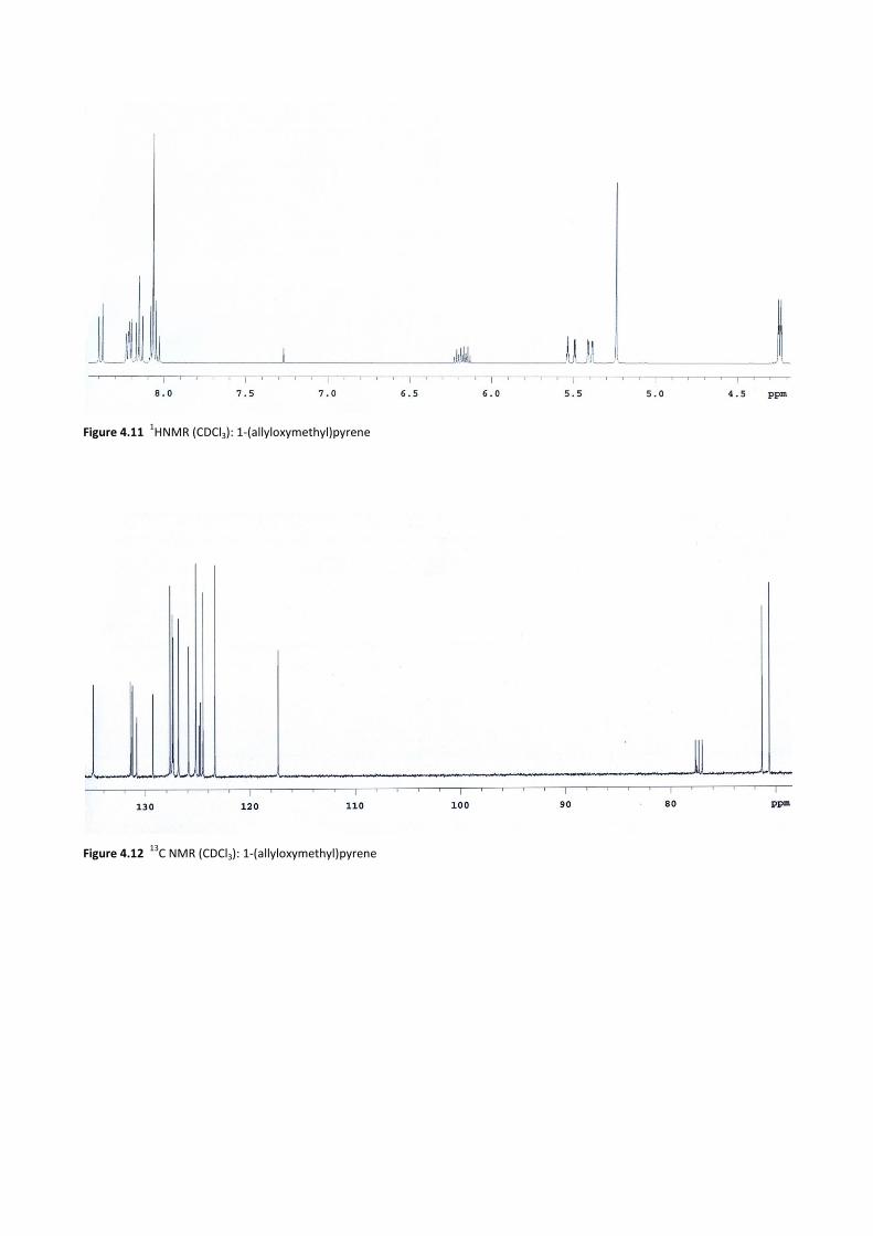
Figure 4.11 1HNMR (CDCl3): 1-(allyloxymethyl)pyrene
Figure 4.12 13
C NMR (CDCl3): 1-(allyloxymethyl)pyrene
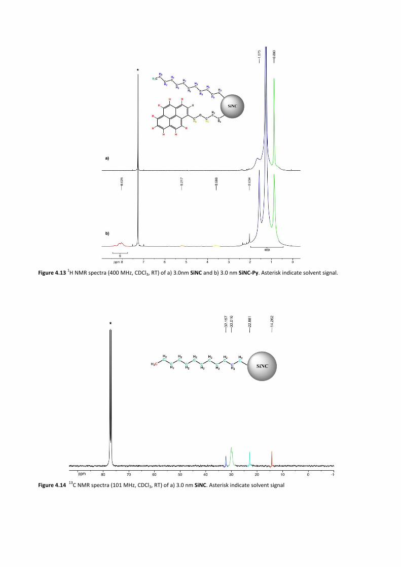
Figure 4.13 1H NMR spectra (400 MHz, CDCl3, RT) of a) 3.0nm SiNC and b) 3.0 nm SiNC-Py. Asterisk indicate solvent signal.
Figure 4.14 13
C NMR spectra (101 MHz, CDCl3, RT) of a) 3.0 nm SiNC. Asterisk indicate solvent signal

Transmission electron spectroscopy (TEM) characterization
The average Si core diameter of the nanocrystals was determined by TEM.
Figures 4.15-4.18 show additional TEM images of the 3.0 nm and 5.0 nm diameter SiNC and SiNC-
Py samples used in the studies. There is no significant difference in size upon Py functionalization.
Figure 4.15 TEM image of 3.0 nm diameter SiNC-Py.
Figure 4.16 TEM image of 3.0 nm diameter SiNC.
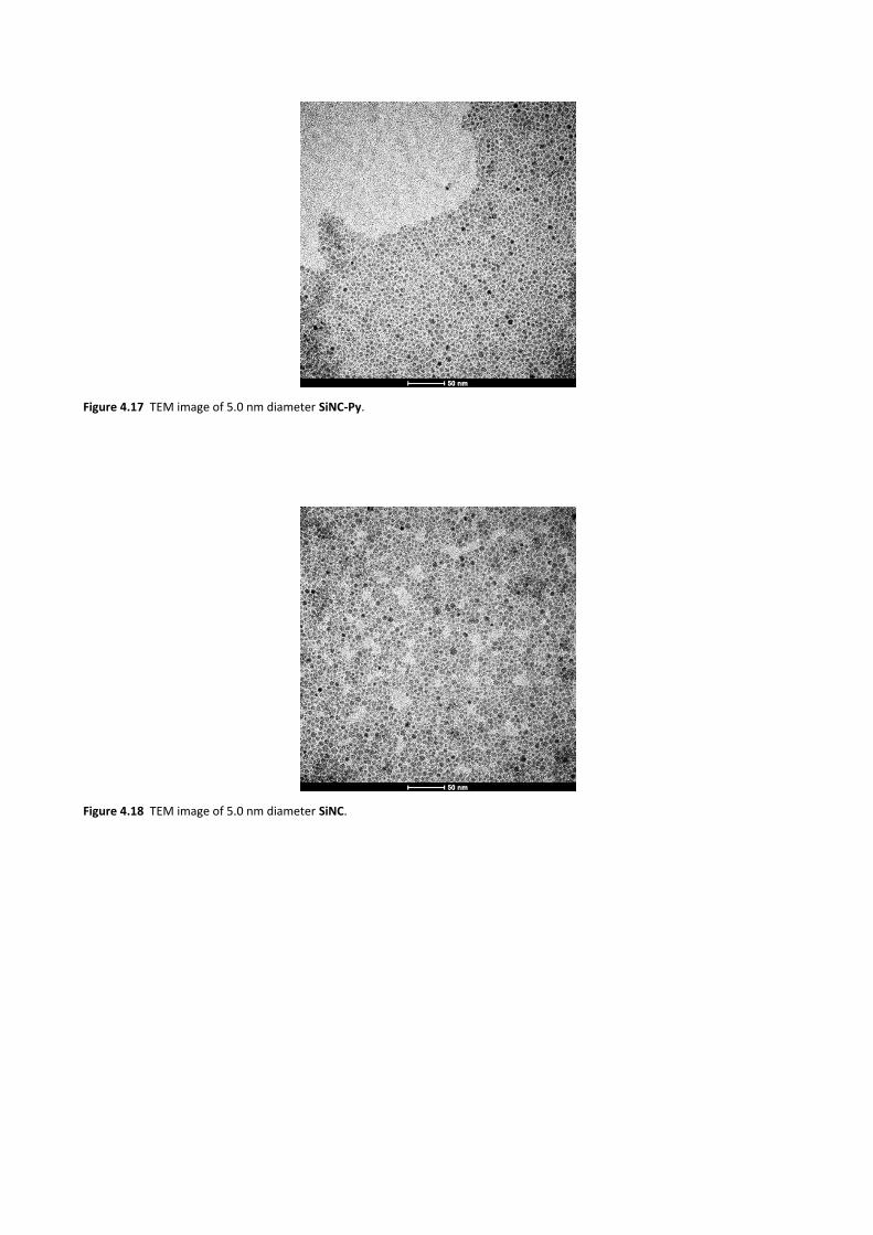
Figure 4.17 TEM image of 5.0 nm diameter SiNC-Py.
Figure 4.18 TEM image of 5.0 nm diameter SiNC.

4.5 Results and Discussion
Optical properties of functionalized SiNCs
Figure 4.19 shows the comparison of optical properties between SiNC and SiNC-Py of 3.0 nm in
toluene dispersion.
The sample control SiNC (without pyrene derivatization) exhibits an unstructured absorption
profile that tails past 500 nm that is characteristic of SiNCs (blue curve in Figure 4.19 a).63
The free chromophore Py (dotted line 4.19 a) has a structured absorption band with three
distinctive peaks in the 300−350 nm region. The contribution of pyrene is highlighted by the
presence of peaks in the SiNC-Py absorbance spectra (red curves in Figure 4.19 a). The number of
pyrene units attached to each SiNC can be estimated from the relative absorbance of the
featureless sloping background associated with the SiNCs and the peaked absorption from the
pyrene.
Figure 4.19 a) absorption profile of 3.0 nm diameter SiNC (blue line), Py (black dotted line), SiNC-Py (red line) in air-equilibrated toluene, b) photoluminescence spectra of SiNC-Py (solid red line, λex = 345 nm; dashed red line, λex = 378 nm) and optically matched solutions of free Py mixed with SiNC in the appropriate ratio (green lines, λex = 345 nm) in air-equilibrated toluene. To obtain the PL spectra in (b) the two samples of SiNC-Py photoexcited at 345 and 378 nm are optically matched at the excitation wavelength to enable direct comparison of the emission intensity of the SiNCs when light absorption is dominated by the pyrene moieties or the nanocrystals. In (b) the y-axes on the left correspond to the pyrene-related emission, and the y-axes on the right correspond to the SiNC-related emission.
On the basis of the molar absorption coefficients for Py and 2.6 nm diameter SiNCs, (ε346 nm(Py) =
4.4 × 10⁴ M−1 cm−1, ε400 nm(SiNC3.0 nm) = 5 × 10⁴ M−1 cm−1,64 there are approximately eight and six
63
Hessel C. M., Reid D., Panthani M. G., Rasch M. R., Goodfellow B. W., Korgel B. A., Chem. Mater. 2012, 24, 393-401. 64
Hessel C. M., Reid D., Panthani M. G., Rasch M. R., Goodfellow B. W., Korgel B. A., Chem. Mater. 2012, 24, 393-401.

pyrene units per nanocrystal for 3.0 nm diameter SiNC-Py made with Py/dodecene ratios of 1:12
(red curve in Figure 4.20 a) and 1:36 (green curve in Figure 4.20 b).
Figure 4.20 (a) Absorbance and (b) photoluminescence spectra ( λex = 378 nm) of 3.0 nm diameter SiNC (blue) and SiNC-Py made
with pyrene:dodecene molar ratios of 1:12 (red line) and 1:36 (green line) dispersed in air-equilibrated toluene. The solutions are
optically matched at the excitation wavelength.
Figure 4.19 b shown the PL spectra of the SiNC-Py samples and SiNCs mixed with free pyrene. The
emission of pyrene at ∼400 nm is observed both when it’s free in solution and when it’s attached
to the SiNCs. There is no evidence of Py excimer emission, which would occur at a longer
wavelength close to 500 nm. The emission of the 3.0 nm nanocrystals was slightly red-shifted from
635 to 680 nm after pyrene passivation (Figure 4.20 b).
To study the influence of the size and chemical surface to optical properties, SiNCs with diameter
of 5 nm have also been synthesized.
UV−vis−NIR absorbance and photoluminescence (PL) spectra of toluene dispersions of the 5.0 nm
diameter SiNC and SiNC-Py are shown in Figure 4.21.

Figure 4.21 a) absorption profile of 5 nm diameter SiNC (blue line), Py (black dotted line), SiNC-Py (red line) in air-equilibrated
toluene, b) photoluminescence spectra of SiNC-Py (solid red line, λex = 345 nm; dashed red line, λex = 378 nm) and optically
matched solutions of free Py mixed with SiNC in the appropriate ratio (green lines, λex = 345 nm) in air-equilibrated toluene. To
obtain the PL spectra in (b) the two samples of SiNC-Py photoexcited at 345 and 378 nm are optically matched at the excitation
wavelength to enable direct comparison of the emission intensity of the SiNCs when light absorption is dominated by the pyrene
moieties or the nanocrystals. In (b) the y-axes on the left correspond to the pyrene-related emission, and the y-axes on the right
correspond to the SiNC-related emission.
The increment of the core size causes a red shift of PL properties. SiNCs exhibit
photoluminescence emission peak at 970 nm (green line in Figure 4.21 b). In this case, pyrene
functionalization does not significantly affect the PL maxima of the SiNC-Py (red line in Figure 4.21
b). The estimate number of pyrene units on the basis of the molar absorption coefficients (ε346
nm(Py) = 4.4 × 10⁴ M−1 cm−1, ε400 nm(SiNC5.0 nm) = 5.3 × 10⁵ M−1 cm−1) is about 60 Py units per
nanocrystal on the 5.0 nm SiNC-Py.
To selectively photoexcite the SiNC core or the ligand, PL emission spectra were measured with
excitation wave-lengths of either λex = 378 or 345 nm.
At 378 nm Py does not absorb the light while at 345nm the majority of the light is absorbed by
pyrene, indeed, pyrene absorbs 67% of the 345 nm light in the case of the 3.0 nm diameter SiNC-
Py.
To evaluate the entity of energy transfer, the PL spectra of SiNC-Py samples in Figure 4.19 b and
Figure 4.21 b were measured at the excitation wavelengths of 378 and 345 nm with the same
photon absorption by optically matching the SiNC-Py dispersions by dilution.
Furthermore, PL spectra were measured for SiNCs mixed with free Py in the appropriate ratios to
match the SiNC-Py absorbance profiles (the green curves in Figure 4.19 b and 4.21 d). When Py is
not attached to the nanocrystals, photoexcitation at 345 nm leads to emission spectra dominated
by the 400 nm emission of pyrene, with a lesser contribution of SiNC emission at longer
wavelength (green curves in Figure 4.19 b and 4.21 d).
In contrast, photoexcitation of the SiNC-Py dispersions with 345 nm light leads predominantly to
emission from the nanocrystals with very little pyrene emission. The Py-related emission band is
largely quenched for both the 3.0 and 5.0 nm diameter SiNC-Py samples, indicative of energy
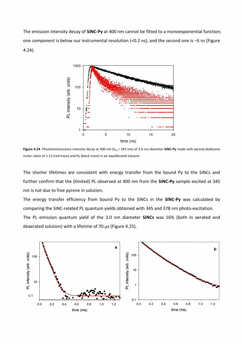
transfer (figure 4.22)
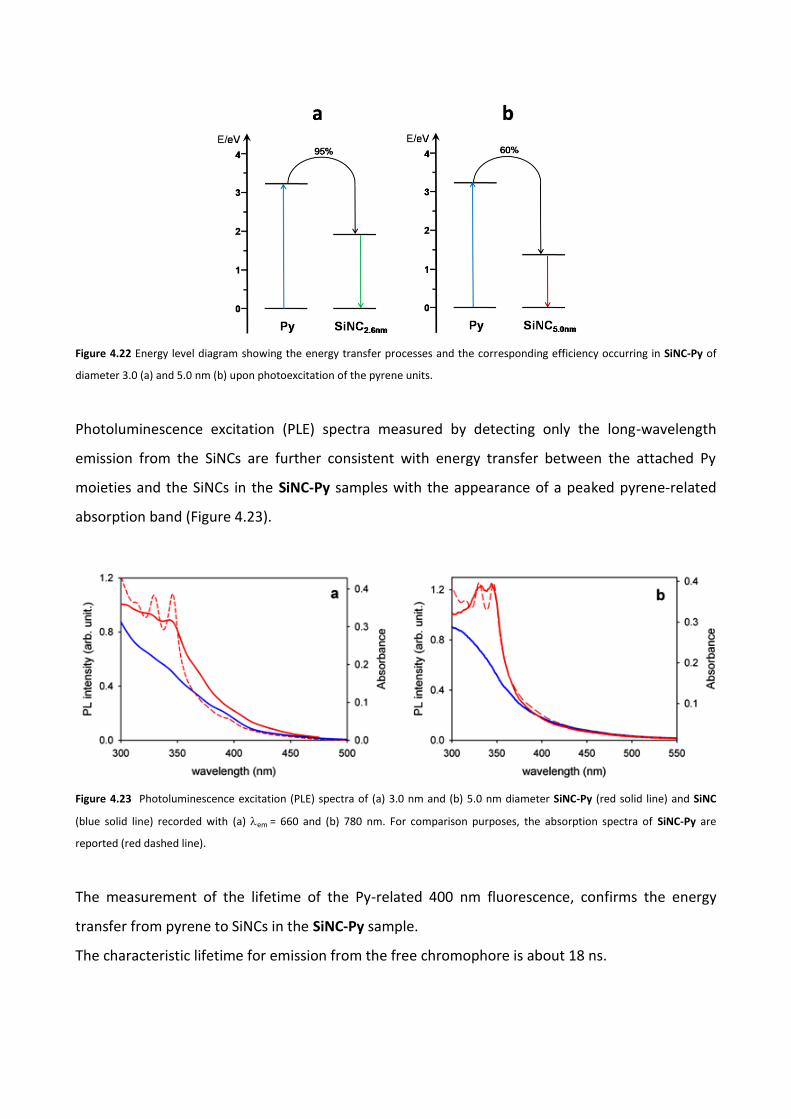
Figure 4.22 Energy level diagram showing the energy transfer processes and the corresponding efficiency occurring in SiNC-Py of
diameter 3.0 (a) and 5.0 nm (b) upon photoexcitation of the pyrene units.
Photoluminescence excitation (PLE) spectra measured by detecting only the long-wavelength
emission from the SiNCs are further consistent with energy transfer between the attached Py
moieties and the SiNCs in the SiNC-Py samples with the appearance of a peaked pyrene-related
absorption band (Figure 4.23).
Figure 4.23 Photoluminescence excitation (PLE) spectra of (a) 3.0 nm and (b) 5.0 nm diameter SiNC-Py (red solid line) and SiNC
(blue solid line) recorded with (a) em = 660 and (b) 780 nm. For comparison purposes, the absorption spectra of SiNC-Py are
reported (red dashed line).
The measurement of the lifetime of the Py-related 400 nm fluorescence, confirms the energy
transfer from pyrene to SiNCs in the SiNC-Py sample.
The characteristic lifetime for emission from the free chromophore is about 18 ns.
The emission intensity decay of SiNC-Py at 400 nm cannot be fitted to a monoexponential function;
one component is below our instrumental resolution (<0.2 ns), and the second one is ∼5 ns (Figure
4.24).
Figure 4.24 Photoluminescence intensity decay at 400 nm (λex = 345 nm) of 3.0 nm diameter SiNC-Py made with pyrene:dodecene
molar ratios of 1:12 (red trace) and Py (black trace) in air-equilibrated toluene.
The shorter lifetimes are consistent with energy transfer from the bound Py to the SiNCs and
further confirm that the (limited) PL observed at 400 nm from the SiNC-Py sample excited at 345
nm is not due to free pyrene in solution.
The energy transfer efficiency from bound Py to the SiNCs in the SiNC-Py was calculated by
comparing the SiNC-related PL quantum yields obtained with 345 and 378 nm photo-excitation.
The PL emission quantum yield of the 3.0 nm diameter SiNCs was 16% (both in aerated and
deaerated solution) with a lifetime of 70 μs (Figure 4.25).
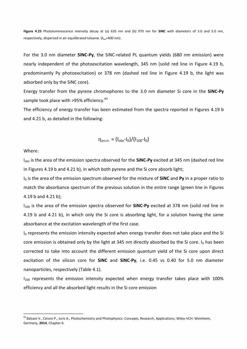
Figure 4.25 Photoluminescence intensity decay at (a) 635 nm and (b) 970 nm for SiNC with diameters of 3.0 and 5.0 nm,
respectively, dispersed in air-equilibrated toluene. (λex=400 nm).
For the 3.0 nm diameter SiNC-Py, the SiNC-related PL quantum yields (680 nm emission) were
nearly independent of the photoexcitation wavelength, 345 nm (solid red line in Figure 4.19 b,
predominantly Py photoexcitation) or 378 nm (dashed red line in Figure 4.19 b, the light was
adsorbed only by the SiNC core).
Energy transfer from the pyrene chromophores to the 3.0 nm diameter Si core in the SiNC-Py
sample took place with >95% efficiency.65
The efficiency of energy transfer has been estimated from the spectra reported in Figures 4.19 b
and 4.21 b, as detailed in the following:
en.tr. = (Iobs-I0)/(I100-I0)
Where:
Iobs is the area of the emission spectra observed for the SiNC-Py excited at 345 nm (dashed red line
in Figures 4.19 b and 4.21 b), in which both pyrene and the Si core absorb light;
I0 is the area of the emission spectrum observed for the mixture of SiNC and Py in a proper ratio to
match the absorbance spectrum of the previous solution in the entire range (green line in Figures
4.19 b and 4.21 b);
I100 is the area of the emission spectra observed for SiNC-Py excited at 378 nm (solid red line in
4.19 b and 4.21 b), in which only the Si core is absorbing light, for a solution having the same
absorbance at the excitation wavelength of the first case.
I0 represents the emission intensity expected when energy transfer does not take place and the Si
core emission is obtained only by the light at 345 nm directly absorbed by the Si core. I0 has been
corrected to take into account the different emission quantum yield of the Si core upon direct
excitation of the silicon core for SiNC and SiNC-Py, i.e. 0.45 vs 0.40 for 5.0 nm diameter
nanoparticles, respectively (Table 4.1).
I100 represents the emission intensity expected when energy transfer takes place with 100%
efficiency and all the absorbed light results in the Si core emission
65
Balzani V., Ceroni P., Juris A., Photochemistry and Photophysics: Concepts, Research, Applications; Wiley-VCH: Weinheim, Germany, 2014, Chapter 6.
Because of the much stronger light absorption of Py compared to that of the SiNCs at 345 nm, Py
functionalization led to a nearly 300% brightness enhancement in SiNC PL.
Pyrene emission was also strongly quenched (>90%) in the 5.0 nm diameter SiNC-Py sample (red
curve, Figure 4.21 b), and the SiNC and SiNC-Py species exhibited PL quantum yields at 970 nm of
45 and 40%, respectively.
The 970 nm PL emission was insensitive to dioxygen, and the luminescence decays of the SiNC and
SiNC-Py were fit to monoexponential functions with lifetimes of 150 and 190 μs, respectively. The
emission quantum yield was high compared to that of dye molecules emitting in the same spectral
region,66 for which emission quantum yields higher than 30% have never been reported, to the
best of our knowledge, and it is comparable to the value recently reported for PbS and PbSe
quantum dots.67
On the basis of the relative PL emission spectra for 5.0 nm diameter SiNC-Py photoexcited with
345 nm (dashed red curve in Figure 4.21 b) and 378 nm light (solid red curve in Figure 4.21 b),
energy transfer from adsorbed pyrene to the SiNCs occurred with 65% efficiency.
With the three-fold enhancement in light absorption due to the adsorbed pyrene, a 40% PL
quantum yield, and a 65% energy transfer efficiency from the pyrene to the SiNCs, there was an
effective enhancement in NIR PL brightness of 78%.
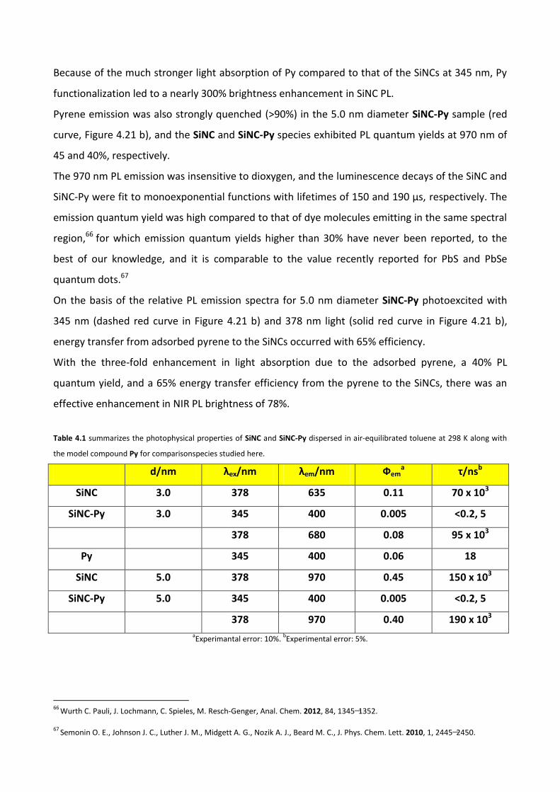
Table 4.1 summarizes the photophysical properties of SiNC and SiNC-Py dispersed in air-equilibrated toluene at 298 K along with
the model compound Py for comparisonspecies studied here.
d/nm λex/nm λem/nm Фema τ/nsb
SiNC 3.0 378 635 0.11 70 x 103
SiNC-Py 3.0 345 400 0.005 <0.2, 5
378 680 0.08 95 x 103
Py 345 400 0.06 18
SiNC 5.0 378 970 0.45 150 x 103
SiNC-Py 5.0 345 400 0.005 <0.2, 5
378 970 0.40 190 x 103
aExperimantal error: 10%.
bExperimental error: 5%.
66
Wurth C. Pauli, J. Lochmann, C. Spieles, M. Resch-Genger, Anal. Chem. 2012, 84, 1345−1352.
67
Semonin O. E., Johnson J. C., Luther J. M., Midgett A. G., Nozik A. J., Beard M. C., J. Phys. Chem. Lett. 2010, 1, 2445−2450.

4.6 Conclusion
This work demonstrates that SiNCs are a viable scaffold for light-harvesting antenna.
Energy transfer between adsorbed pyrene units and SiNCs occurs with relatively high efficiency,
and pyrene functionalization does not deteriorate the SiNC PL properties. These materials
represent a family of nanocrystals with significantly enhanced PL brightness as a result of the
attachment of light-harvesting antenna that promote light emission from the nanocrystals as a
result of energy transfer. The PL brightness of the 3.0 nm diameter nanocrystals is enhanced by
nearly 300%. The 5.0 nm diameter SiNC-Py exhibits UV-sensitized NIR luminescence with high
emission quantum yield and long lifetime (Table 1), even in the presence of dioxygen.
Chapter 5
Interaction between pyrene-functionalized
Silicon nanocrystals and carbon allotropes
5.1 Introduction
Here, we study the effect of the distance between the chromophore and the Si nanocrystal core
on the sensitized light emission of the Si core.
Silicon nanocrystals with average core diameter of 3 and 5 nm were passivated with dodecene by
thermal hydrosilylation and coupled to pyrene (Py) derivative molecules with C11 (SiNC(C11)Py) or
C3 alkyl tethers (SiNC(C3)Py) via a terminal alkene (Figure 5.1). We also studied the electronic
interactions of these nanocrystals associated with carbon allotropes: C60, single-walled carbon
nanotubes (SWCNTs), and graphene. Additional energy transfer processes were found to occur
from the SiNC to these carbon materials.
5.2 Thermal hydrosililation of SiNCs with 1-
(allyloxymethyl)pyrene (C3) and 1-((undec-10-en-1-
yloxy)methyl)pyrene (C11)
Through the thermal reduction of HSQ and etching with a solution of HF and HCl, hydride-
terminated SiNCs have been synthesized as described in the Chapter 4.
The SiNCs were functionalized by thermal hydrosilylation with a combination of ligands: 1-
dodecene and pyrene chromophore (Py) binds different alkyl length chains (Figure 1).

To evaluate the influence of the chromophore on optical properties, SiNCs were also passivated
with only 1-dodecene (SiNC).
Figure 5.1
5.2.1 Experimental details
Materials: hydrofluoric acid (48% in H2O), 1-dodecene, 1-pyrenemethanol, sodium hydride, 11-
bromide-1-undecene were purchased from Sigma Aldrich.
1-(allyloxymethyl)pyrene (Py) synthesis: Sodium hydride (0.124 g, 5.16 mmol, 1.2 eq) was added
to a mixture of 1-pyrenemethanol (1.00 g, 4.30 mmol, 1eq), propargyl bromide (0.645 g, 5.33

mmol, 1.24 eq) in CH3CN (25 mL) at 70°C. The reaction mixture was stirred vigorously for 24 h at
70°C. After completion of the reaction, three drops of H2O were added to the reaction mixture to
quench the reaction. The mixture was extracted into chloroform (3 x 5 mL). The chloroform layer
was dried over MgSO4 and the solvent was removed under reduced pressure to give the crude
product. The resulting residue was purified by silica column chromatography (Hexane/ EtOAc 8:2),
to give the product as a yellow solid (750 mg, yield = 66 %).
1H-NMR (400 MHz, CDCl3) δ:8.38 (d, J = 9.2 Hz, 1H); 8.23-8.20 (m, 2H); 8.17-8.13 (m, 2H); 8.08-
8.03 (m, 4H); 6.21-6.14 (m, 1H); 5.51 (dd, J1 = 1.6 Hz, J2 = 1.6 Hz, 1H); 5.39 (dd, J1 = 1.6 Hz, J2 = 1.6
Hz, 1H); 5.24 (s, 2H); 4.25-4.23 (m, 2H).
13C-NMR (100 MHz, CDCl3) δ:134.9, 131.4; 131.3; 131.2; 130.8; 129.2; 127.6; 127.4; 127.3; 126.8;
125.8; 125.2; 125.1; 124.9; 124.7; 124.5; 123.3; 117.3; 71.2, 70.6.ESI-MS : 232 [M- C3H5]+
Synthesis of 1-((undec-10-enyloxy)methyl)pyrene. To a mixture of 1-pyrenemethanol (1.00 g,
4.30 mmol, 1eq), 11-bromide-1-undecene (1.504 g, 6.45 mmol, 1.5 eq) in CH3CN (25 mL) was
added sodium hydride (0.124 g, 5.16 mmol, 1.2 eq) at 80 °C. The reaction mixture was stirred
vigorously for 48 h at 70°C. After completion of the reaction, three drops of H2O were added to
quench the reaction. The mixture was extracted (3 × 5 mL) with chloroform. The chloroform layer
was dried over MgSO4 and the solvent was removed under reduced pressure to give the solid
crude product. The resulting residue was purified by silica column chromatography (hexane/
AcOEt 8:2), to give the product as a yellow solid (yield = 80 %). 1H-NMR (400 MHz, CDCl3) δ: 8.41
(d, J = 9.2 Hz, 1H); 8.24-8.20 (m, 2H); 8.19-8.14 (m, 2H); 8.10-8.04 (m, 4H); 6.02-6.04 (m, 1H); 5.23
(s, 2H); 5.08 (d, J = 17.2 Hz, 1H); 5.03 (d, J = 10.4, 1H); 3.64 (t, J = 6.4 Hz, 2H); 2.13-2.07 (m, 2H);
1.75-1.69 (m, 2H); 1.42-1.40 (m, 4H); 1.53-1.30 (m, 8H). 13C-NMR (100 MHz, CDCl3) δ: 139.0, 131.7;
131.1; 131.0; 130.6; 129.1; 127.3; 127.2; 127.0; 126.6; 125.6; 124.9; 124.7; 124.6; 124.2; 123.3;
114.0; 71.2; 70.3; 33.7; 29.7; 29.4; 29.3; 29.0; 28.2; 26.1. ESI-MS : 407 [M + Na]; 215 [M-
C11H21O ]+
SiNC, SiNC(C3)Py and SiNC(C11)Py synthesis. The synthetic procedure follows the method
developed by Hessel, et al.68 Generally, 40 mL of Fox-16 (hydrogen silsesquioxane 16 wt%) is dried
under vacuum and the resulting white solid is then transferred to a tube furnace and annealed at
68
Hessel C. M., Henderson E. J., Veinot J. G. C., Chem. Mater. 2006, 18, 6139-6146.
1100°C (3.0 nm diameter) or 1200°C (5.0 nm diameter) at a heating rate of 18°C/min and held at
that temperature for an hour under reducing atmosphere (93% N2, 7% H2).
The SiNC/SiO2 composite is etched with 48% HF and 37.5% HCl (10:1 v/v) in the dark for 4-6 hours
and then centrifuged at 8000 rpm for 5 min. The H-terminated SiNCs are then rinsed once with
deionized (DI) water, twice with ethanol, and once with chloroform. The nanocrystals are
dispersed in 5 mL of 1-dodecene with 490 mg of 1-(allyloxymethyl)pyrene (1:12 pyrene:dodecene
molar ratio) to obtain SiNC(C3)Py sample, in 5 mL of 1-dodecene to have SiNC and 4 mL of 1-
dodecene with 250 mg of 1-((undec-10-en-1-yloxy)methyl)pyrene (1:27 pyrene:dodecene molar
ratio) for SiNC(C11)Py. The initially turbid dispersions are put through three freeze-pump-thaw
cycles, and then heated to 170°C under N2 flow for 12 hours. Over time, the dispersions become
optically clear, indicating that passivation of Si nanocrystals has occurred. To purify the
nanocrystals, the solutions are transferred to a glass centrifuge tube, spin at 8000 rpm for 5 min
and discard the precipitate (poorly capped SiNCs) on the bottom. The supernatant is transferred
to another glass centrifuge tube and undergoes many centrifugation/precipitation cycles using
toluene/ethanol solvent/antisolvent pair. The final SiNC, SiNC(C3)Py, SiNC(C11)Py samples were
dispersed in toluene at a concentration of 3-5 mg/mL until further characterization.
5.3 Material characterization
Transmission electron spectroscopy (TEM) characterization
The nanocrystals were synthesized at either 1100°C or 1200°C to obtain different sizes. The
average diameters were determined by TEM of 2.9±0.7 nm and 5.3±2.0 nm, respectively (Figure
5.2).

Figure 5.2 STEM-HAADF micrographs of two families of SiNC(C11)Py nanocrystals, with nominal diameters of 3 nm (a) and 5 nm (b).
In the inset the size distribution histograms are obtained by manually measuring the size of the nanocrystals. Histograms are fitted
with a Lognormal distribution, and the mean value and the FWHM of the distributions, of 2.9 and 5.3 nm respectively, are reported.
X-ray diffraction (XRD)
Figure 5.3 shows X-ray diffraction of SiNC(C11)Py of 3 and 5 nm. Both samples present narrow
peaks at 28°, 48°, 56° corresponding to reflections from the (111), (220) and (311) crystallographic
planes of diamond cubic Si (PDF # 027–1402, a=b=c=5.43088 Å).
Figure 5.3 XRD (=0.154 nm). A reference diffraction pattern is provided for diamond cubic Si in (a) (PDF # 027–1402,
a=b=c=5.43088 Å).

X-ray photoelectron spectroscopy
X-ray photoelectron spectroscopy (XPS) confirms the covalent functionalization of SiNC(C11)Py (3
and 5 nm) with the peak at 102 eV corresponding to the formation of Si-C bonds on the
nanocrystals surface (Figure 5.4).
Figure 5.4 XPS of 3 and 5 nm diameter SiNC(C11)Py.
FTIR spectroscopy
The FTIR spectrum of SiNC (Figure 5.5) shows features due to ν(C−H) stretching at 3000-2850 cm-1
and δ(C−H) bending at 1500-1350 cm-1; the presence of the oxygen is evidenced by the strong ν(Si−
O) stretching at 1024 cm-1. For SiNC(C11)Py the covalent attachment of the ligand to the surface is
confirmed by the presence of aromatic ν(C−H) stretching at 3100-2890 cm-1, ν(C=C) stretching at
1640 cm-1 and δ(C−H) bending at 1480 cm-1 and 940-800 cm-1. There is no evidence of ν(Si-H) (ca.
2100 cm-1) consistent with effective functionalization.
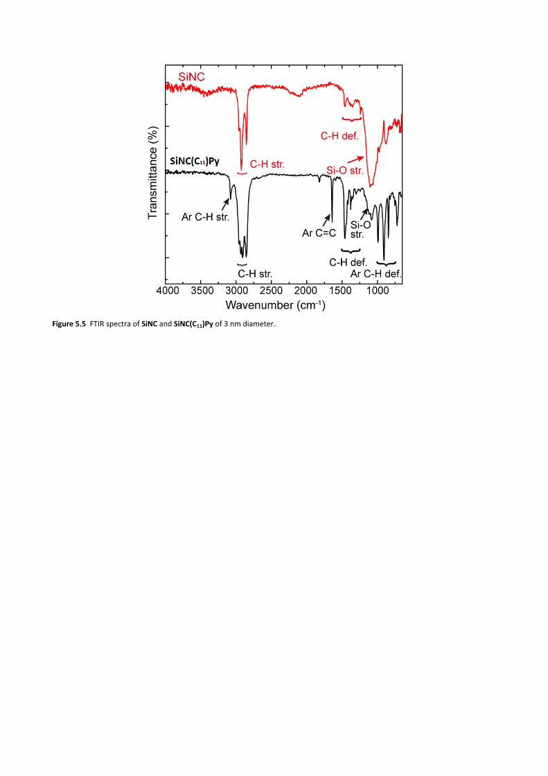
Figure 5.5 FTIR spectra of SiNC and SiNC(C11)Py of 3 nm diameter.
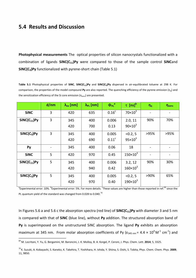
5.4 Results and Discussion
Photophysical measurements The optical properties of silicon nanocrystals functionalized with a
combination of ligands SiNC(C11)Py were compared to those of the sample control SiNCand
SiNC(C3)Py functionalized with pyrene-short chain (Table 5.1)
Table 5.1 Photophysical properties of SiNC, SiNC(C11)Py and SiNC(C3)Py dispersed in air-equilibrated toluene at 298 K. For
comparison, the properties of the model compound Py are also reported. The quenching efficiency of the pyrene emission (ηq) and
the sensitization efficiency of the Si core emission (ηsens) are presented.
d/nm λex [nm] λPL [nm] PLa [ns]b ηq ηsens
SiNC 3 420 635 0.16c 70×103 - -
SiNC(C11)Py 3 345
420
400
700
0.006
0.13
2.0, 11
90×103
90% 70%
SiNC(C3)Py 3 345
420
400
690
0.005
0.11c
<0.2, 5
95×103
>95% >95%
Py - 345 400 0.06 18 - -
SiNC 5 420 970 0.45 150×103 - -
SiNC(C11)Py 5 345
420
400
940
0.006
0.42
3.2, 12
160×103
90% 30%
SiNC(C3)Py 5 345
420
400
970
0.005
0.40
<0.2, 5
190×103
>90% 65%
aExperimental error: 10%.
bExperimental error: 5%. For more details.
cThese values are higher than those reported in ref.
69 since the
PL quantum yield of the standard was changed from 0.028 to 0.040.70
In Figures 5.6 a and 5.6 c the absorption spectra (red line) of SiNC(C11)Py with diameter 3 and 5 nm
is compared with that of SiNC (blue line), without Py addition. The structured absorption band of
Py is superimposed on the unstructured SiNC absorption. The ligand Py exhibits an absorption
maximum at 345 nm. From molar absorption coefficients of Py (ε345 nm = 4.4 × 10⁴ M-1 cm-1) and
69
M. Locritani, Y. Yu, G. Bergamini, M. Baroncini, J. K. Molloy, B. A. Korgel, P. Ceroni, J. Phys. Chem. Lett. 2014, 5, 3325.
70
K. Suzuki, A. Kobayashi, S. Kaneko, K. Takehira, T. Yoshihara, H. Ishida, Y. Shiina, S. Oishi, S. Tobita, Phys. Chem. Chem. Phys. 2009, 11, 9850.
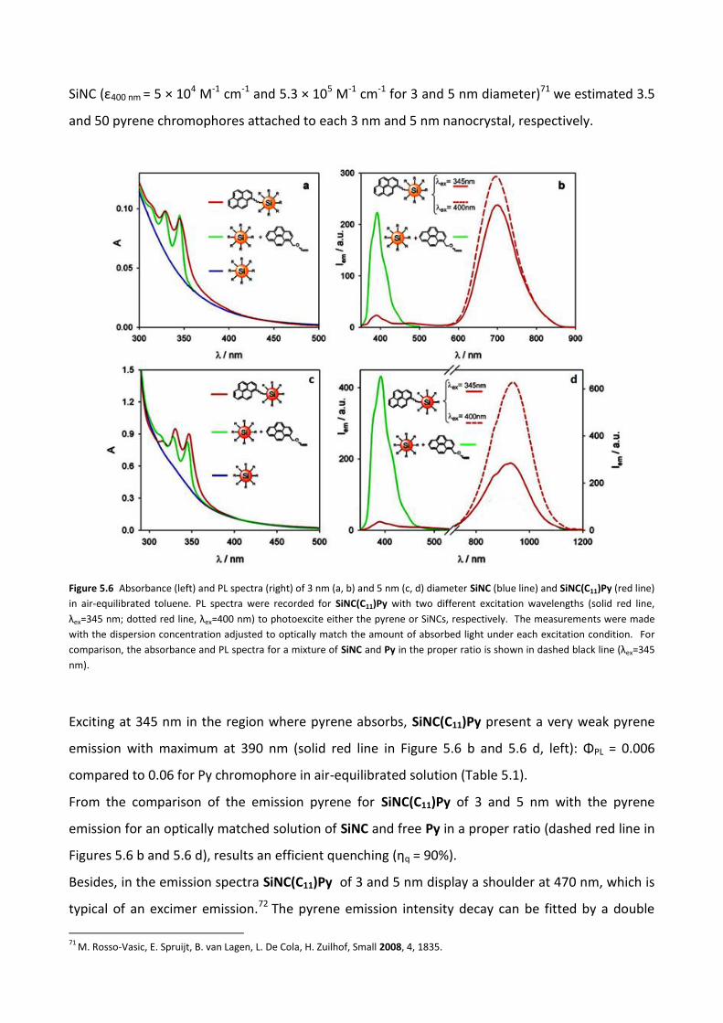
SiNC (ε400 nm = 5 × 10⁴ M-1 cm-1 and 5.3 × 10⁵ M-1 cm-1 for 3 and 5 nm diameter)71 we estimated 3.5
and 50 pyrene chromophores attached to each 3 nm and 5 nm nanocrystal, respectively.
Figure 5.6 Absorbance (left) and PL spectra (right) of 3 nm (a, b) and 5 nm (c, d) diameter SiNC (blue line) and SiNC(C11)Py (red line)
in air-equilibrated toluene. PL spectra were recorded for SiNC(C11)Py with two different excitation wavelengths (solid red line,
λex=345 nm; dotted red line, λex=400 nm) to photoexcite either the pyrene or SiNCs, respectively. The measurements were made
with the dispersion concentration adjusted to optically match the amount of absorbed light under each excitation condition. For
comparison, the absorbance and PL spectra for a mixture of SiNC and Py in the proper ratio is shown in dashed black line (λex=345
nm).
Exciting at 345 nm in the region where pyrene absorbs, SiNC(C11)Py present a very weak pyrene
emission with maximum at 390 nm (solid red line in Figure 5.6 b and 5.6 d, left): ΦPL = 0.006
compared to 0.06 for Py chromophore in air-equilibrated solution (Table 5.1).
From the comparison of the emission pyrene for SiNC(C11)Py of 3 and 5 nm with the pyrene
emission for an optically matched solution of SiNC and free Py in a proper ratio (dashed red line in
Figures 5.6 b and 5.6 d), results an efficient quenching (ηq = 90%).
Besides, in the emission spectra SiNC(C11)Py of 3 and 5 nm display a shoulder at 470 nm, which is
typical of an excimer emission.72 The pyrene emission intensity decay can be fitted by a double
71
M. Rosso-Vasic, E. Spruijt, B. van Lagen, L. De Cola, H. Zuilhof, Small 2008, 4, 1835.

exponential (Table 5.1), in which the shorter component is assigned to the quenched pyrene
monomer, while the longer component to the pyrene excimer. Indeed, the percentage of the
longer lifetime increases by recording the emission intensity at 470 nm compared to that at 400
nm. SiNC(C3)Py does not manifest the presence of the excimer emission (Figure 5.7).
Figure 5.7 Normalized emission spectra of SiNC(C3)Py (red line) and SiNC(C11)Py (black line) of the pyrene chromophore in toluene
solution at room temperature. λex = 345 nm.
The pyrene chromophores are embedded within the dodecyl ligand layer on the nanocrystals
when linked by the shorter C3 tether, which eliminates the interaction between pyrene units;
whereas, the longer C11 tether places the Py units far enough away from the dodecene monolayer
that *Py-Py interactions become possible.
Photoexcitation of the Si core at 400 nm gives rise to similar PL spectra for both the SiNC(C11)Py
and SiNC.
Py does not absorb any light at this wavelength.
In SiNC(C11)Py of 3 nm a slight decrease of the emission quantum yield (13% compared to 16% for
SiNC, Table 5.1) is accompanied by a red shift of the emission maximum (Figure 5.8 a) and a slight
increase of the luminescent decay lifetime, which is in the range of 90 μs (Table 1).
72
V. Balzani, P. Ceroni, A. Juris, Wiley-VCH, Weinheim, 2014, pp. 139–168.
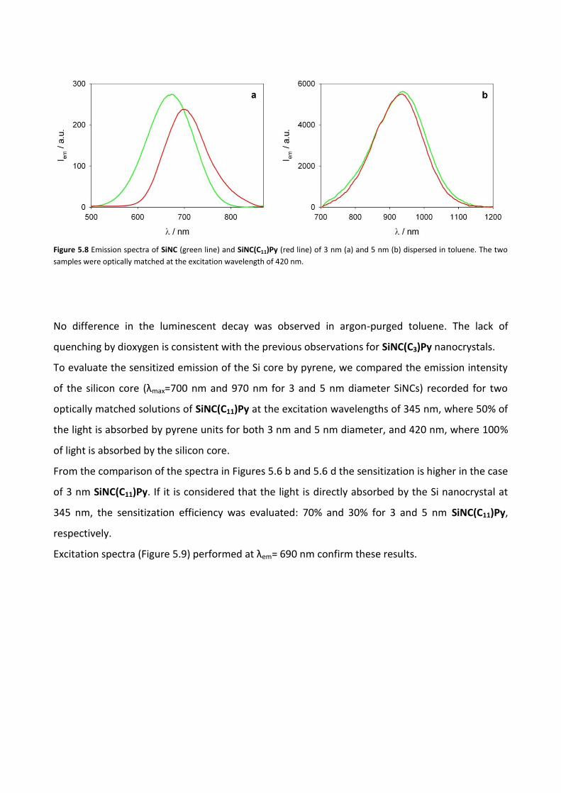
Figure 5.8 Emission spectra of SiNC (green line) and SiNC(C11)Py (red line) of 3 nm (a) and 5 nm (b) dispersed in toluene. The two
samples were optically matched at the excitation wavelength of 420 nm.
No difference in the luminescent decay was observed in argon-purged toluene. The lack of
quenching by dioxygen is consistent with the previous observations for SiNC(C3)Py nanocrystals.
To evaluate the sensitized emission of the Si core by pyrene, we compared the emission intensity
of the silicon core (λmax=700 nm and 970 nm for 3 and 5 nm diameter SiNCs) recorded for two
optically matched solutions of SiNC(C11)Py at the excitation wavelengths of 345 nm, where 50% of
the light is absorbed by pyrene units for both 3 nm and 5 nm diameter, and 420 nm, where 100%
of light is absorbed by the silicon core.
From the comparison of the spectra in Figures 5.6 b and 5.6 d the sensitization is higher in the case
of 3 nm SiNC(C11)Py. If it is considered that the light is directly absorbed by the Si nanocrystal at
345 nm, the sensitization efficiency was evaluated: 70% and 30% for 3 and 5 nm SiNC(C11)Py,
respectively.
Excitation spectra (Figure 5.9) performed at λem= 690 nm confirm these results.

Figure 5.9 Excitation spectra of 3 nm diameter SiNC(C11)Py (red solid line) and SiNC (blue solid line) recorded with em= 690 nm.
For comparison purposes, the absorption spectrum of SiNC(C11)Py is reported (red dashed line).
The sensitization efficiency is lower than that observed for the SiNC(C3)Py (Table 1) because of the
longer average distance between pyrene and Si core which slows down the energy transfer
process. On the other hand, the quenching efficiency of pyrene is only slightly lower than in
SiNC(C3)Py because in the case of SiNC(C11)Py, the radiative decay of the fluorescent pyrene
monomer excited state competes, not only with the energy transfer process, but also with excimer
formation.
5.5 Interaction of silicon nanocrystals with carbon-based
materials
When the tether length is long enough to allow the Py units to extend away from the dodecene
passivation layer into the solution, it provides the possibility for Py interactions with other
molecules and surfaces in the surrounding environment. This is not the case when the Py units are
buried in the ligand passivation layer. The observation of excimer formation for the long-tether
SiNC(C11)Py units indicates that the Py is exposed significantly to the surroundings. It is well-
known that pyrene interacts strongly with carbon allotropes like carbon nanotubes and

graphene.73,74 Therefore, a series of tests exposing SiNC(C11)Py to C60, carbon nanotubes and
graphene was performed (Figure 5.10).
Figure 5.10
73
X. An, T. Simmons, R. Shah, C. Wolfe, K. M. Lewis, M. Washington, S. K. Nayak, S. Talapatra, S. Kar, Nano Lett. 2010, 10, 4295. 74
A. Schlierf, H. Yang, E. Gebremedhn, E. Treossi, L. Ortolani, L. Chen, A. Minoia, V. Morandi, P. Samori, C. Casiraghi, D. Beljonne, V. Palermo, Nanoscale 2013, 5, 4205.
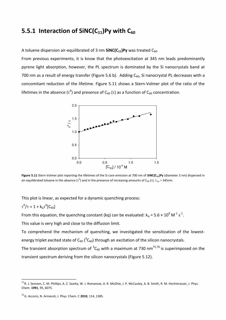
5.5.1 Interaction of SiNC(C11)Py with C60
A toluene dispersion air-equilibrated of 3 nm SiNC(C11)Py was treated C60.
From previous experiments, it is know that the photoexcitation at 345 nm leads predominantly
pyrene light absorption, however, the PL spectrum is dominated by the Si nanocrystals band at
700 nm as a result of energy transfer (Figure 5.6 b). Adding C60, Si nanocrystal PL decreases with a
concomitant reduction of the lifetime. Figure 5.11 shows a Stern-Volmer plot of the ratio of the
lifetimes in the absence (0) and presence of C60 () as a function of C60 concentration.
Figure 5.11 Stern-Volmer plot reporting the lifetimes of the Si core emission at 700 nm of SiNC(C11)Py (diameter 3 nm) dispersed in
air-equilibrated toluene in the absence (0) and in the presence of increasing amounts of C60 (). ex = 345nm.
This plot is linear, as expected for a dynamic quenching process:
0/ = 1 + kq
0[C60]
From this equation, the quenching constant (kq) can be evaluated: kq = 5.6 × 10⁹ M-1 s-1.
This value is very high and close to the diffusion limit.
To comprehend the mechanism of quenching, we investigated the sensitization of the lowest-
energy triplet excited state of C60 (3C60) through an excitation of the silicon nanocrystals.
The transient absorption spectrum of 3C60 with a maximum at 730 nm75,76 is superimposed on the
transient spectrum deriving from the silicon nanocrystals (Figure 5.12).
75
R. J. Sension, C. M. Phillips, A. Z. Szarka, W. J. Romanow, A. R. McGhie, J. P. McCauley, A. B. Smith, R. M. Hochstrasser, J. Phys. Chem. 1991, 95, 6075. 76
G. Accorsi, N. Armaroli, J. Phys. Chem. C 2010, 114, 1385.
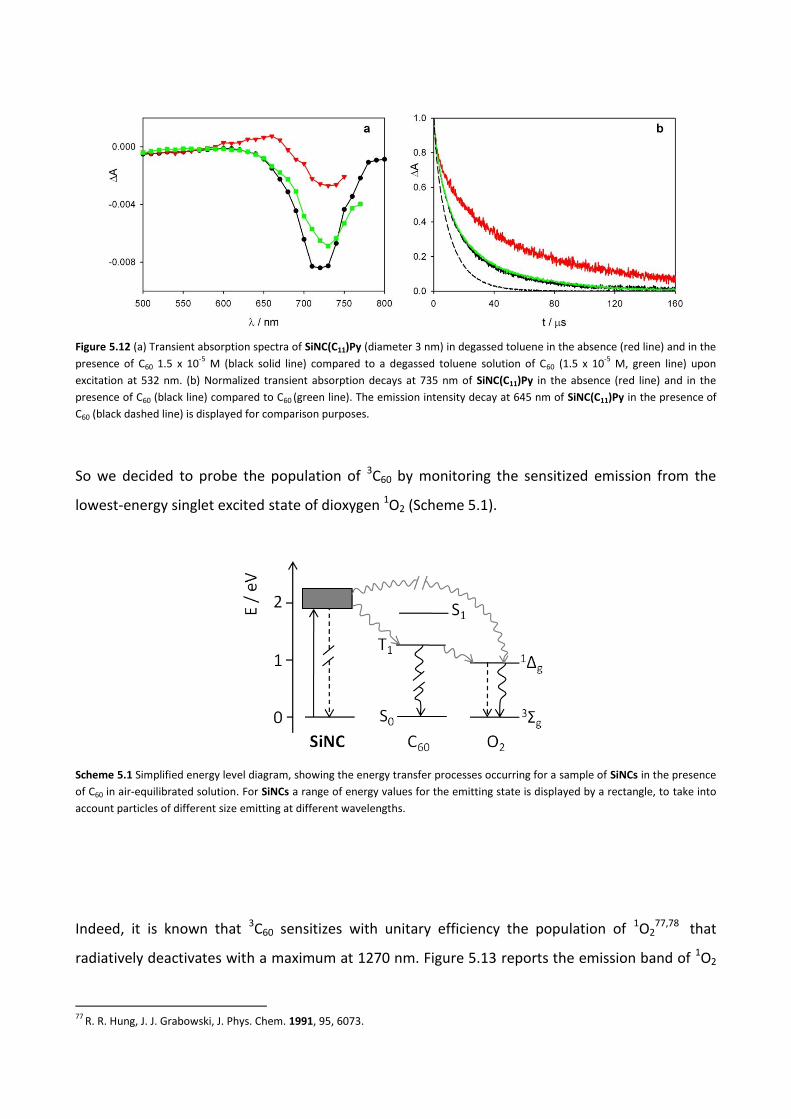
Figure 5.12 (a) Transient absorption spectra of SiNC(C11)Py (diameter 3 nm) in degassed toluene in the absence (red line) and in the
presence of C60 1.5 x 10⁻⁵
M (black solid line) compared to a degassed toluene solution of C60 (1.5 x 10⁻⁵
M, green line) upon
excitation at 532 nm. (b) Normalized transient absorption decays at 735 nm of SiNC(C11)Py in the absence (red line) and in the
presence of C60 (black line) compared to C60 (green line). The emission intensity decay at 645 nm of SiNC(C11)Py in the presence of
C60 (black dashed line) is displayed for comparison purposes.
So we decided to probe the population of 3C60 by monitoring the sensitized emission from the
lowest-energy singlet excited state of dioxygen 1O2 (Scheme 5.1).
Scheme 5.1 Simplified energy level diagram, showing the energy transfer processes occurring for a sample of SiNCs in the presence
of C60 in air-equilibrated solution. For SiNCs a range of energy values for the emitting state is displayed by a rectangle, to take into
account particles of different size emitting at different wavelengths.
Indeed, it is known that 3C60 sensitizes with unitary efficiency the population of 1O277,78 that
radiatively deactivates with a maximum at 1270 nm. Figure 5.13 reports the emission band of 1O2
77
R. R. Hung, J. J. Grabowski, J. Phys. Chem. 1991, 95, 6073.
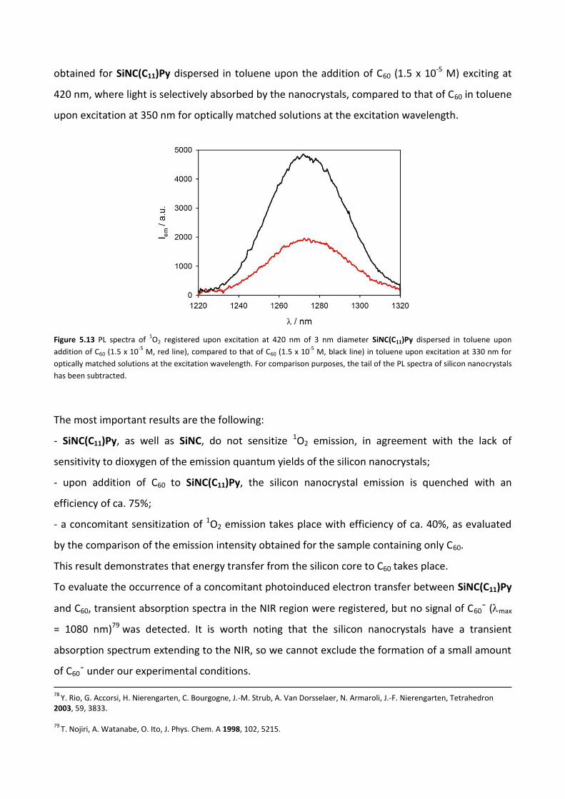
obtained for SiNC(C11)Py dispersed in toluene upon the addition of C60 (1.5 x 10⁻⁵ M) exciting at
420 nm, where light is selectively absorbed by the nanocrystals, compared to that of C60 in toluene
upon excitation at 350 nm for optically matched solutions at the excitation wavelength.
Figure 5.13 PL spectra of 1O2 registered upon excitation at 420 nm of 3 nm diameter SiNC(C11)Py dispersed in toluene upon
addition of C60 (1.5 x 10⁻⁵
M, red line), compared to that of C60 (1.5 x 10⁻⁵
M, black line) in toluene upon excitation at 330 nm for
optically matched solutions at the excitation wavelength. For comparison purposes, the tail of the PL spectra of silicon nanocrystals
has been subtracted.
The most important results are the following:
- SiNC(C11)Py, as well as SiNC, do not sensitize 1O2 emission, in agreement with the lack of
sensitivity to dioxygen of the emission quantum yields of the silicon nanocrystals;
- upon addition of C60 to SiNC(C11)Py, the silicon nanocrystal emission is quenched with an
efficiency of ca. 75%;
- a concomitant sensitization of 1O2 emission takes place with efficiency of ca. 40%, as evaluated
by the comparison of the emission intensity obtained for the sample containing only C60.
This result demonstrates that energy transfer from the silicon core to C60 takes place.
To evaluate the occurrence of a concomitant photoinduced electron transfer between SiNC(C11)Py
and C60, transient absorption spectra in the NIR region were registered, but no signal of C60ˉ (max
= 1080 nm)79 was detected. It is worth noting that the silicon nanocrystals have a transient
absorption spectrum extending to the NIR, so we cannot exclude the formation of a small amount
of C60ˉ under our experimental conditions.
78
Y. Rio, G. Accorsi, H. Nierengarten, C. Bourgogne, J.-M. Strub, A. Van Dorsselaer, N. Armaroli, J.-F. Nierengarten, Tetrahedron 2003, 59, 3833. 79
T. Nojiri, A. Watanabe, O. Ito, J. Phys. Chem. A 1998, 102, 5215.
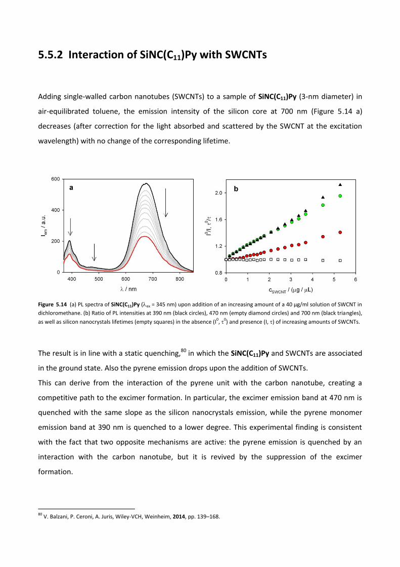
5.5.2 Interaction of SiNC(C11)Py with SWCNTs
Adding single-walled carbon nanotubes (SWCNTs) to a sample of SiNC(C11)Py (3-nm diameter) in
air-equilibrated toluene, the emission intensity of the silicon core at 700 nm (Figure 5.14 a)
decreases (after correction for the light absorbed and scattered by the SWCNT at the excitation
wavelength) with no change of the corresponding lifetime.
Figure 5.14 (a) PL spectra of SiNC(C11)Py (ex = 345 nm) upon addition of an increasing amount of a 40 μg/ml solution of SWCNT in
dichloromethane. (b) Ratio of PL intensities at 390 nm (black circles), 470 nm (empty diamond circles) and 700 nm (black triangles),
as well as silicon nanocrystals lifetimes (empty squares) in the absence (I0,
0) and presence (I, ) of increasing amounts of SWCNTs.
The result is in line with a static quenching,80 in which the SiNC(C11)Py and SWCNTs are associated
in the ground state. Also the pyrene emission drops upon the addition of SWCNTs.
This can derive from the interaction of the pyrene unit with the carbon nanotube, creating a
competitive path to the excimer formation. In particular, the excimer emission band at 470 nm is
quenched with the same slope as the silicon nanocrystals emission, while the pyrene monomer
emission band at 390 nm is quenched to a lower degree. This experimental finding is consistent
with the fact that two opposite mechanisms are active: the pyrene emission is quenched by an
interaction with the carbon nanotube, but it is revived by the suppression of the excimer
formation.
80
V. Balzani, P. Ceroni, A. Juris, Wiley-VCH, Weinheim, 2014, pp. 139–168.

TEM of the adduct formed by SWCNTs and SiNC(C11)Py further confirms the ground state
interaction. The HRTEM and STEM-HAADF micrographs (Figure 5.15) highlight that nanocrystals
are preferentially located on the SWCNTs rather than on the carbon film coated copper grid.
Figure 5.15 (a) TEM micrograph and (b) STEM-HAADF micrograph of SWCNTs coated by SiNC(C11)Py.
5.5.3 Interaction of SiNC(C11)Py with graphene
The interaction of SiNC(C11)Py (3 and 5 nm diameter) with graphene was evaluated in a different
way. The lack of dispersibility of exfoliated graphene in a solvent suitable for SiNC(C11)Py,
complicates the study of solution phase behavior.
Therefore, we immersed a graphene film grown by Chemical Vapor Deposition (CVD) (details on
the growth are reported in Ortolani et al.)81 in a solution of the nanocrystal, and we studied their
interaction.
The nanocrystals (Figure 5.16) form a uniformly dispersed monolayer of nanoparticles, without the
formation of thick aggregates. The very low thickness of the graphene film, between 1 and 3 layers,
allows us to obtain a deeper insight on the crystalline structure of the nanoparticles, by enhancing
the contrast for a light element such as silicon, as previously reported by Panthani et al.82
81
L. Ortolani, E. Cadelano, G. P. Veronese, C. Degli Esposti Boschi, E. Snoeck, L. Colombo, V. Morandi, Nano Lett. 2012, 12, 5207.
82
M. G. Panthani, C. M. Hessel, D. Reid, G. Casillas, M. José-Yacamán, B. A. Korgel, J. Phys. Chem. C 2012, 116, 22463.

Figure 5.16 Low magnification TEM micrographs of 3 nm (a) and 5 nm (b) SiNC(C11)Py deposited on CVD graphene. (c,d) High
magnification HRTEM image of a supported on graphene, showing the Si (111) lattice fringes at 0.31 nm.
The emission intensity of SiNC(C11)Py (3 nm diameter) is lower than the graphene layer, as
evidenced by both the PL spectrum and the wide-field luminescence image reported in (Figure
5.17).
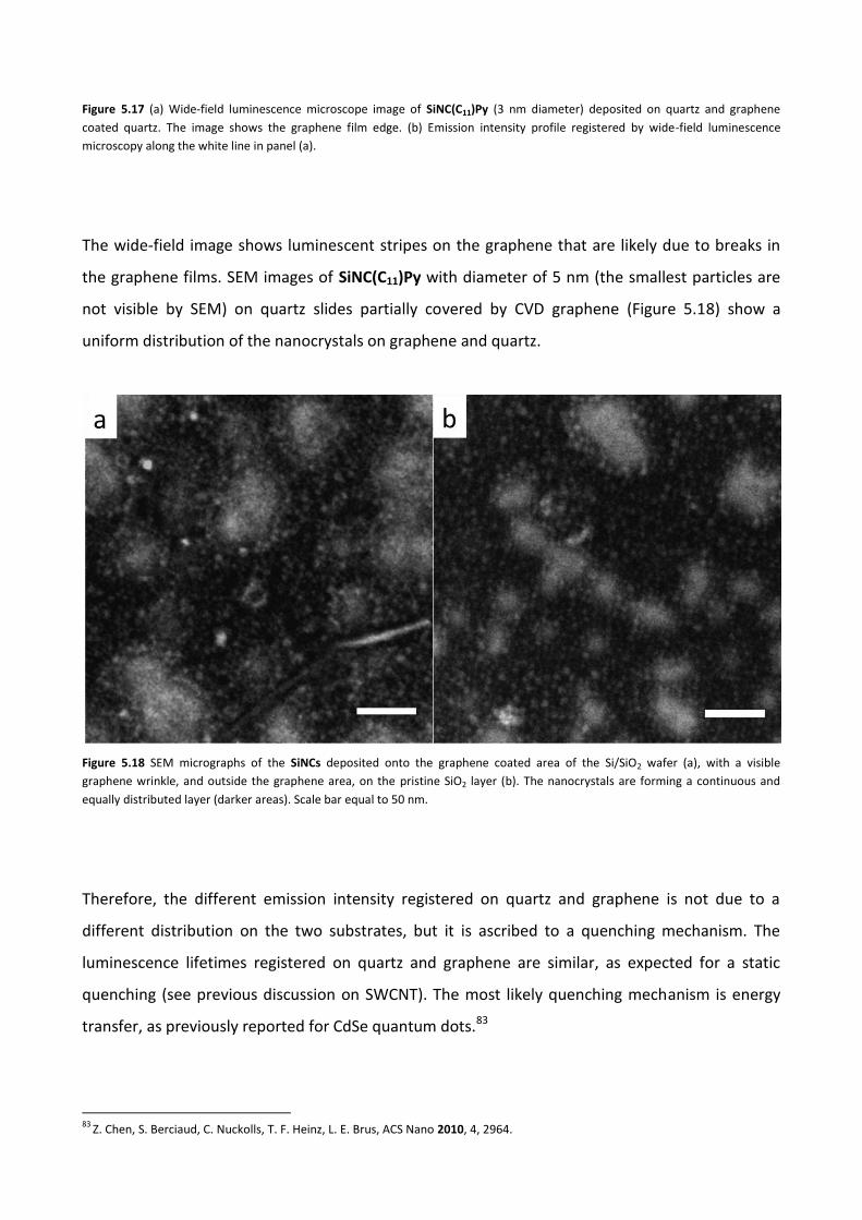
Figure 5.17 (a) Wide-field luminescence microscope image of SiNC(C11)Py (3 nm diameter) deposited on quartz and graphene
coated quartz. The image shows the graphene film edge. (b) Emission intensity profile registered by wide-field luminescence
microscopy along the white line in panel (a).
The wide-field image shows luminescent stripes on the graphene that are likely due to breaks in
the graphene films. SEM images of SiNC(C11)Py with diameter of 5 nm (the smallest particles are
not visible by SEM) on quartz slides partially covered by CVD graphene (Figure 5.18) show a
uniform distribution of the nanocrystals on graphene and quartz.
Figure 5.18 SEM micrographs of the SiNCs deposited onto the graphene coated area of the Si/SiO2 wafer (a), with a visible
graphene wrinkle, and outside the graphene area, on the pristine SiO2 layer (b). The nanocrystals are forming a continuous and
equally distributed layer (darker areas). Scale bar equal to 50 nm.
Therefore, the different emission intensity registered on quartz and graphene is not due to a
different distribution on the two substrates, but it is ascribed to a quenching mechanism. The
luminescence lifetimes registered on quartz and graphene are similar, as expected for a static
quenching (see previous discussion on SWCNT). The most likely quenching mechanism is energy
transfer, as previously reported for CdSe quantum dots.83
83
Z. Chen, S. Berciaud, C. Nuckolls, T. F. Heinz, L. E. Brus, ACS Nano 2010, 4, 2964.

5.6 Conclusion
The covalent passivation of SiNCs surface allow to exploit the new properties that emerge from
the interaction of SiNCs with chromophores.
The chromophores can be exploited as light-harvesting antenna: exciting the pyrene
chromophores, energy transfer occurs and sensitized emission of the nanocrystals is observed.
The length of the link between the pyrene unit and the silicon core influences the efficiency of this
System.
Tethers that are long enough for the pyrene to extend beyond the capping ligand layer into the
surrounding solution enable association with molecules and substrates in the surroundings, such
as the carbon allotropes studied here: C60, single-walled carbon nanotubes (SWCNTs) and
graphene.
Energy transfer process can occur either to or from the Si nanocrystals. Energy is transferred from
the organic chromophore to the silicon core in the case of pyrene; whereas, energy flows from the
quantum dots to nearby fullerenes to populate their lowest energy triplet excited state. This
means that electronic energy harvested by the hybrid SiNC(C11)Py material can be further
exploited by an interaction with external systems.
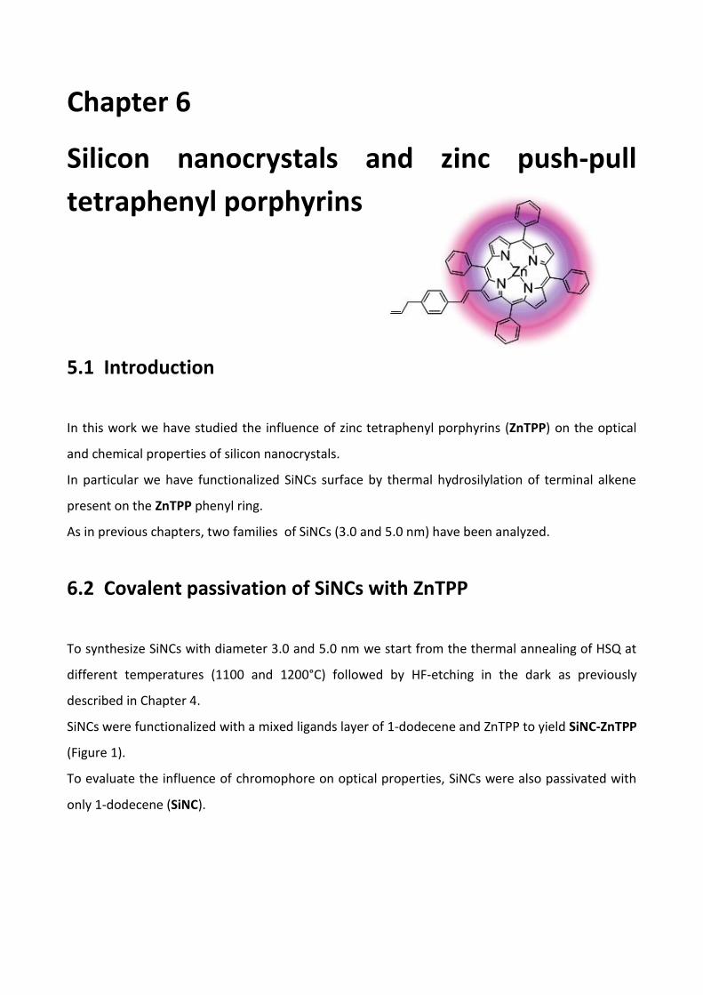
Chapter 6
Silicon nanocrystals and zinc push-pull
tetraphenyl porphyrins
5.1 Introduction
In this work we have studied the influence of zinc tetraphenyl porphyrins (ZnTPP) on the optical
and chemical properties of silicon nanocrystals.
In particular we have functionalized SiNCs surface by thermal hydrosilylation of terminal alkene
present on the ZnTPP phenyl ring.
As in previous chapters, two families of SiNCs (3.0 and 5.0 nm) have been analyzed.
6.2 Covalent passivation of SiNCs with ZnTPP
To synthesize SiNCs with diameter 3.0 and 5.0 nm we start from the thermal annealing of HSQ at
different temperatures (1100 and 1200°C) followed by HF-etching in the dark as previously
described in Chapter 4.
SiNCs were functionalized with a mixed ligands layer of 1-dodecene and ZnTPP to yield SiNC-ZnTPP
(Figure 1).
To evaluate the influence of chromophore on optical properties, SiNCs were also passivated with
only 1-dodecene (SiNC).

Figure 6.1
6.2.1 Experimental details
SiNC, SiNC-ZnTPP synthesis: the synthetic procedure follows the method developed by Hessel, et
al.84 Generally, 40 mL of Fox-16 (hydrogen silsesquioxane 16 wt%) is dried under vacuum and the
resulting white solid is then transferred to a tube furnace and annealed at 1100°C (3.0 nm
diameter) or 1200°C (5.0 nm diameter) at a heating rate of 18°C/min and held at that temperature
for an hour under reducing atmosphere (93% N2, 7% H2).
The SiNC/SiO2 composite is etched with 48% HF and 37.5% HCl (10:1 v/v) in the dark for 4-6 hours
and then centrifuged at 8000 rpm for 5 min. The H-terminated SiNCs are then rinsed once with
deionized (DI) water, twice with ethanol, and once with chloroform. The nanocrystals are
dispersed in 4 mL of 1-dodecene to have SiNC and 4 mL of 1-dodecene with 300 mg of ZnTPP
(1:50 zinc porphyrin:dodecene molar ratio) for SiNC-ZnTPP. The initially turbid dispersions are put
through three freeze-pump-thaw cycles, and then heated to 170°C under N2 flow for 12 hours.
Over time, the dispersions become optically clear, indicating that passivation of Si nanocrystals has
occurred.
84
Hessel C. M., Henderson E. J., Veinot J. G. C., Chem. Mater. 2006, 18, 6139-6146.
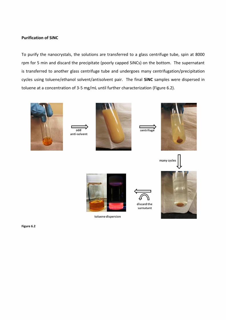
Purification of SiNC
To purify the nanocrystals, the solutions are transferred to a glass centrifuge tube, spin at 8000
rpm for 5 min and discard the precipitate (poorly capped SiNCs) on the bottom. The supernatant
is transferred to another glass centrifuge tube and undergoes many centrifugation/precipitation
cycles using toluene/ethanol solvent/antisolvent pair. The final SiNC samples were dispersed in
toluene at a concentration of 3-5 mg/mL until further characterization (Figure 6.2).
Figure 6.2

Purification of SiNC-ZnTPP
To purify the nanocrystals, the solutions are transferred to a glass centrifuge tube, spin at 8000
rpm for 5 min and discard the precipitate (poorly capped SiNCs) on the bottom. The supernatant is
transferred to another glass centrifuge tube and undergoes many centrifugation/precipitation
cycles using toluene/ethanol solvent/antisolvent pair. The final SiNC-ZnTPP samples were
dispersed in toluene at a concentration of 3-5 mg/mL until further characterization (Figure 6.2).
Figure 6.3
6.3 Material characterization
Transmission electron spectroscopy (TEM) characterization
The average Si core diameter of the nanocrystals was determined by TEM.
Figures 6.4-6.5 show TEM images of the 3.0 nm and 5.0 nm diameter SiNC-ZnTPP samples used in
the studies. The functionalization does not alter the size of SiNCs.
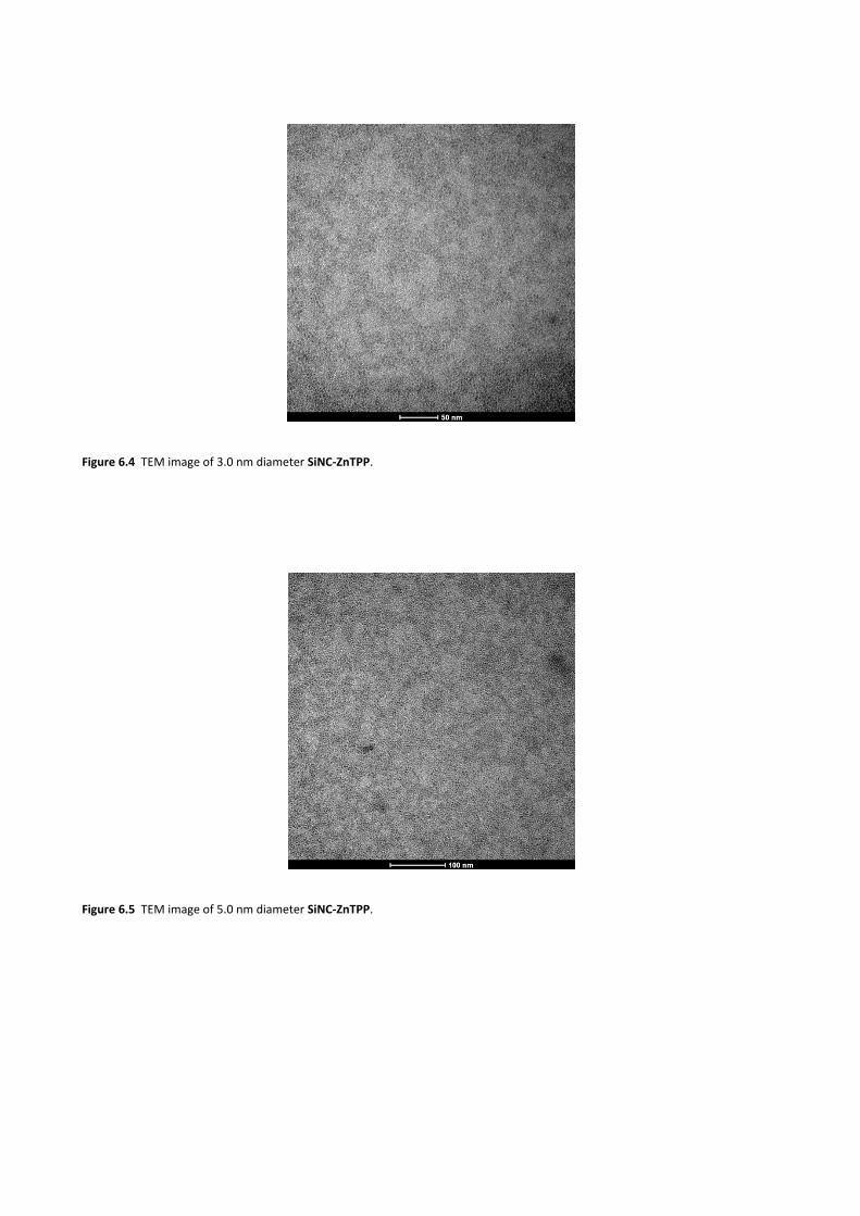
Figure 6.4 TEM image of 3.0 nm diameter SiNC-ZnTPP.
Figure 6.5 TEM image of 5.0 nm diameter SiNC-ZnTPP.
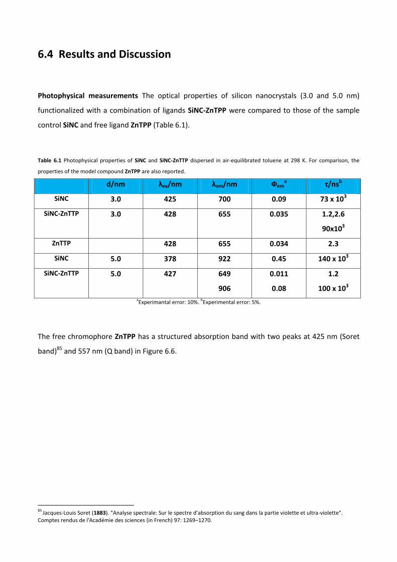
6.4 Results and Discussion
Photophysical measurements The optical properties of silicon nanocrystals (3.0 and 5.0 nm)
functionalized with a combination of ligands SiNC-ZnTPP were compared to those of the sample
control SiNC and free ligand ZnTPP (Table 6.1).
Table 6.1 Photophysical properties of SiNC and SiNC-ZnTTP dispersed in air-equilibrated toluene at 298 K. For comparison, the
properties of the model compound ZnTPP are also reported.
d/nm λex/nm λem/nm Фema τ/nsb
SiNC 3.0 425 700 0.09 73 x 103
SiNC-ZnTTP 3.0 428 655 0.035 1.2,2.6
90x103
ZnTTP 428 655 0.034 2.3
SiNC 5.0 378 922 0.45 140 x 103
SiNC-ZnTTP 5.0 427 649
906
0.011
0.08
1.2
100 x 103 aExperimantal error: 10%.
bExperimental error: 5%.
The free chromophore ZnTPP has a structured absorption band with two peaks at 425 nm (Soret
band)85 and 557 nm (Q band) in Figure 6.6.
85
Jacques-Louis Soret (1883). "Analyse spectrale: Sur le spectre d’absorption du sang dans la partie violette et ultra-violette". Comptes rendus de l'Académie des sciences (in French) 97: 1269–1270.
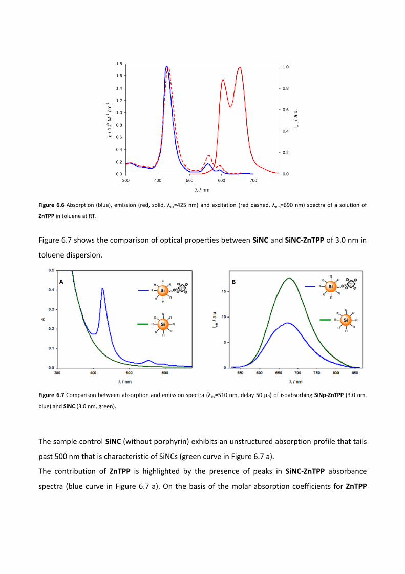
Figure 6.6 Absorption (blue), emission (red, solid, λex=425 nm) and excitation (red dashed, λem=690 nm) spectra of a solution of
ZnTPP in toluene at RT.
Figure 6.7 shows the comparison of optical properties between SiNC and SiNC-ZnTPP of 3.0 nm in
toluene dispersion.
Figure 6.7 Comparison between absorption and emission spectra (λex=510 nm, delay 50 μs) of isoabsorbing SiNp-ZnTPP (3.0 nm,
blue) and SiNC (3.0 nm, green).
The sample control SiNC (without porphyrin) exhibits an unstructured absorption profile that tails
past 500 nm that is characteristic of SiNCs (green curve in Figure 6.7 a).
The contribution of ZnTPP is highlighted by the presence of peaks in SiNC-ZnTPP absorbance
spectra (blue curve in Figure 6.7 a). On the basis of the molar absorption coefficients for ZnTPP
/ nm
300 400 500 600 700
/
10
5 M
-1 c
m-1
0.0
0.2
0.4
0.6
0.8
1.0
1.2
1.4
1.6
1.8
I em
/ a
.u.
0.0
0.2
0.4
0.6
0.8
1.0
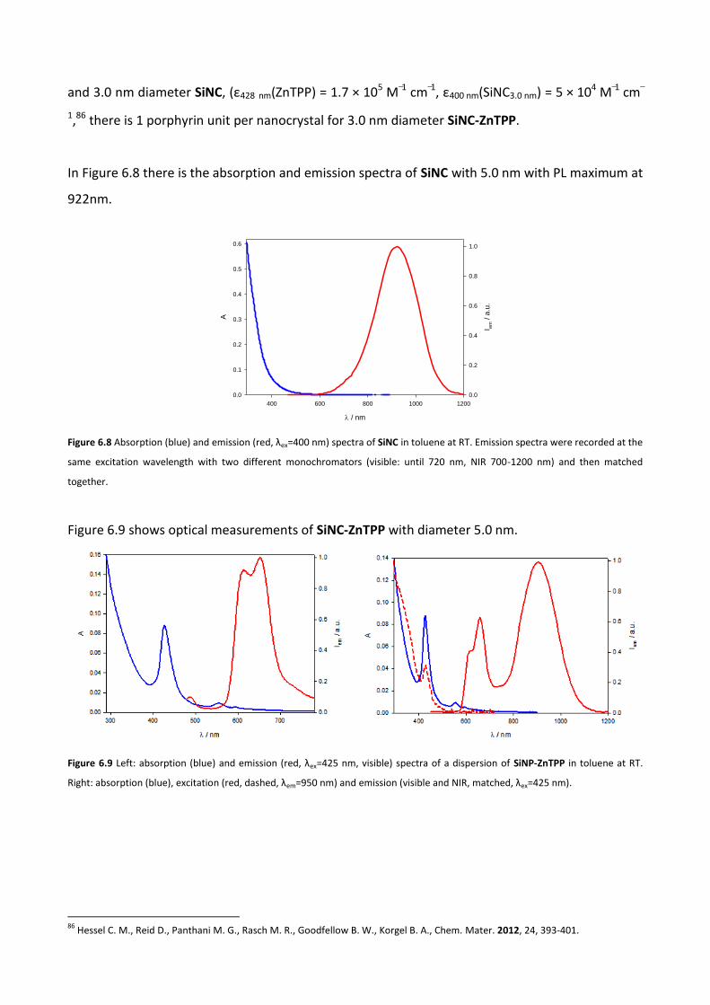
and 3.0 nm diameter SiNC, (ε428 nm(ZnTPP) = 1.7 × 10⁵ M−1 cm
−1, ε400 nm(SiNC3.0 nm) = 5 × 10⁴ M−1 cm
−
1,86 there is 1 porphyrin unit per nanocrystal for 3.0 nm diameter SiNC-ZnTPP.
In Figure 6.8 there is the absorption and emission spectra of SiNC with 5.0 nm with PL maximum at
922nm.
Figure 6.8 Absorption (blue) and emission (red, λex=400 nm) spectra of SiNC in toluene at RT. Emission spectra were recorded at the
same excitation wavelength with two different monochromators (visible: until 720 nm, NIR 700-1200 nm) and then matched
together.
Figure 6.9 shows optical measurements of SiNC-ZnTPP with diameter 5.0 nm.
Figure 6.9 Left: absorption (blue) and emission (red, λex=425 nm, visible) spectra of a dispersion of SiNP-ZnTPP in toluene at RT.
Right: absorption (blue), excitation (red, dashed, λem=950 nm) and emission (visible and NIR, matched, λex=425 nm).
86
Hessel C. M., Reid D., Panthani M. G., Rasch M. R., Goodfellow B. W., Korgel B. A., Chem. Mater. 2012, 24, 393-401.
/ nm
400 600 800 1000 1200
A
0.0
0.1
0.2
0.3
0.4
0.5
0.6
I em
/ a
.u.
0.0
0.2
0.4
0.6
0.8
1.0

In order to investigate the quenching of the porphyrin unit and the energy transfer from the dye
to the particle, we added free ZnTPP to a dispersion of SiNC. This mixture is properly diluted until
absorbance at 427 nm (corresponding to the Soret peak of the free ZnTPP) is the same of a
dispersion of SiNC-ZnTPP.
Exciting at the same wavelength, we recorded emission spectra of the two solutions in the visible
region, in the same conditions: emission in the visibile region coming from SiNC-ZnTPP is partially
quenched (integration is 1/3 in respect of the mixed sample), while its emission lifetime decreases
from 2.2 ns to 1.2 ns. Similar results were evidenced in a similar experiment, considering
isoabsorbing solutions at 558 nm (in correspondence of the lower Q-bands of the porphyrinic
unity).
Excitation spectrum recorded for emission at 950 nm shows a peak at 425 nm, pointing out an
energy transfer from the ZnTPP moiety to the Si nanoparticle (Figure 6.9).
Figure 6.10 Absorption (dashed lines) and emission (solid lines) spectra of a dispersion of SiNC-ZnTPP(216) in toluene (blue) and a
mix solution of ZnTPP and SiNC (red line) (λex=427 nm).
To evaluate the entity of energy transfer we made the comparison between NIR emission spectra
of isoabsorbing dispersion of SiNC and SiNC-ZnTPP.
/ nm
400 500 600 700 800
A
0.00
0.05
0.10
0.15
0.20
I em
/ a
.u.
0
20
40
60
80
100
120
140
160
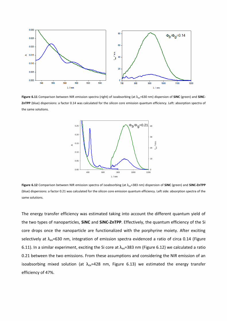
Figure 6.11 Comparison between NIR emission spectra (right) of isoabsorbing (at λex=630 nm) dispersion of SiNC (green) and SiNC-
ZnTPP (blue) dispersions: a factor 0.14 was calculated for the silicon core emission quantum efficiency. Left: absorption spectra of
the same solutions.
Figure 6.12 Comparison between NIR emission spectra of isoabsorbing (at λex=383 nm) dispersion of SiNC (green) and SiNC-ZnTPP
(blue) dispersions: a factor 0.21 was calculated for the silicon core emission quantum efficiency. Left side: absorption spectra of the
same solutions.
The energy transfer efficiency was estimated taking into account the different quantum yield of
the two types of nanoparticles, SiNC and SiNC-ZnTPP. Effectively, the quantum efficiency of the Si
core drops once the nanoparticle are functionalized with the porphyrine moiety. After exciting
selectively at λex=630 nm, integration of emission spectra evidenced a ratio of circa 0.14 (Figure
6.11). In a similar experiment, exciting the Si core at λex=383 nm (Figure 6.12) we calculated a ratio
0.21 between the two emissions. From these assumptions and considering the NIR emission of an
isoabsorbing mixed solution (at λex=428 nm, Figure 6.13) we estimated the energy transfer
efficiency of 47%.
/ nm
400 600 800 1000 1200
A
0.00
0.05
0.10
0.15
0.20
0.25
I em
/ a
.u.
0
10
20
30
40bg=0.21
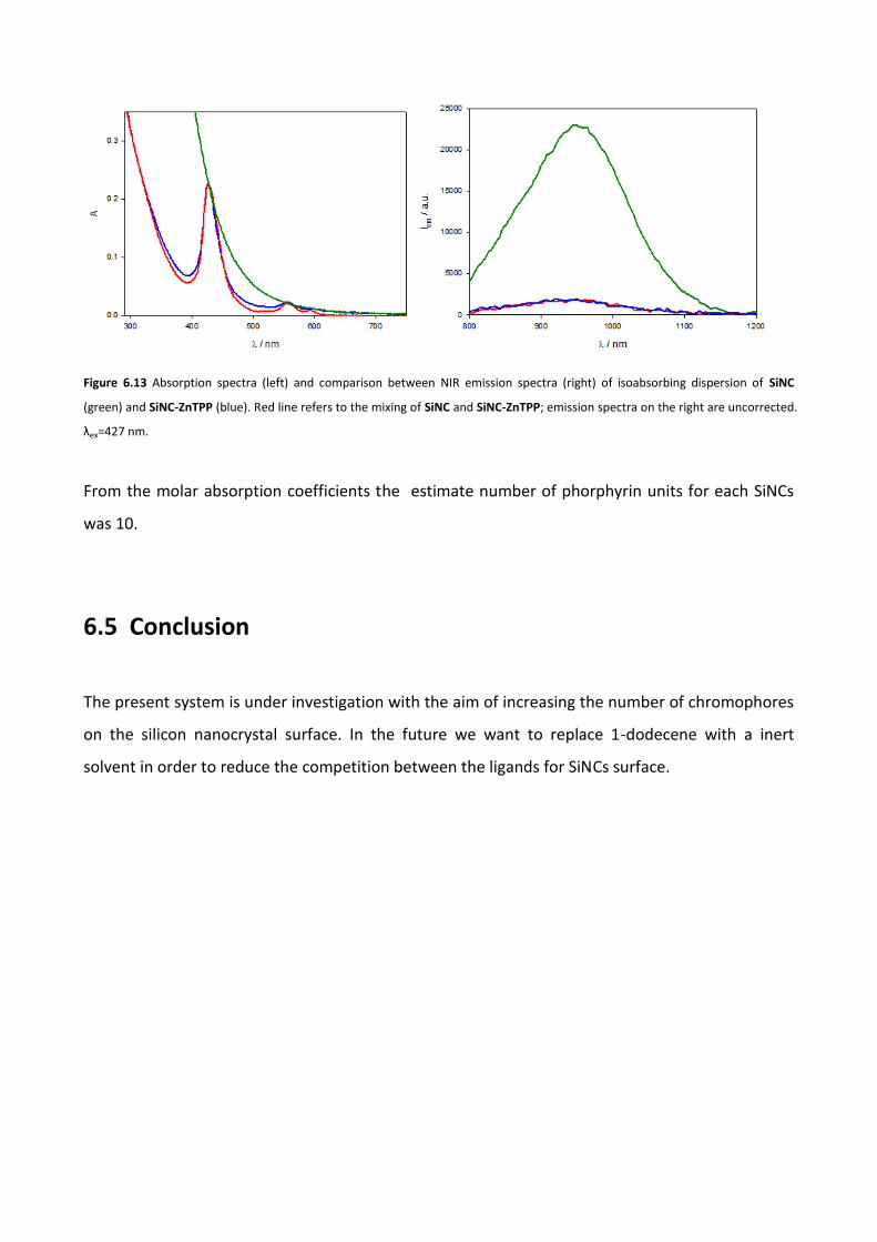
Figure 6.13 Absorption spectra (left) and comparison between NIR emission spectra (right) of isoabsorbing dispersion of SiNC
(green) and SiNC-ZnTPP (blue). Red line refers to the mixing of SiNC and SiNC-ZnTPP; emission spectra on the right are uncorrected.
λex=427 nm.
From the molar absorption coefficients the estimate number of phorphyrin units for each SiNCs
was 10.
6.5 Conclusion
The present system is under investigation with the aim of increasing the number of chromophores
on the silicon nanocrystal surface. In the future we want to replace 1-dodecene with a inert
solvent in order to reduce the competition between the ligands for SiNCs surface.
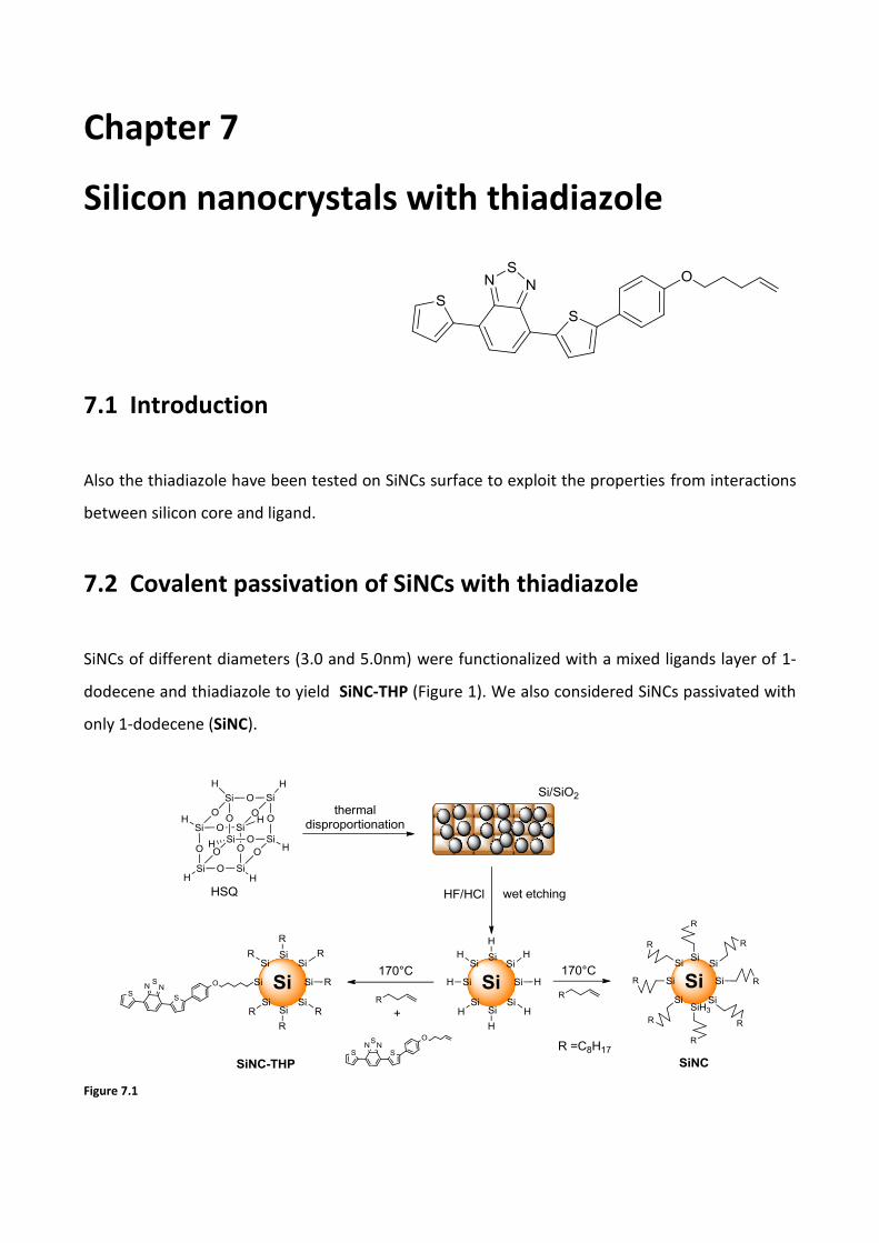
Chapter 7
Silicon nanocrystals with thiadiazole
7.1 Introduction
Also the thiadiazole have been tested on SiNCs surface to exploit the properties from interactions
between silicon core and ligand.
7.2 Covalent passivation of SiNCs with thiadiazole
SiNCs of different diameters (3.0 and 5.0nm) were functionalized with a mixed ligands layer of 1-
dodecene and thiadiazole to yield SiNC-THP (Figure 1). We also considered SiNCs passivated with
only 1-dodecene (SiNC).
Figure 7.1
7.2.1 Experimental details
SiNC, SiNC-THP synthesis: the synthetic procedure follows the method developed by Hessel, et
al.87 Generally, 40 mL of Fox-16 (hydrogen silsesquioxane 16 wt%) is dried under vacuum and the
resulting white solid is then transferred to a tube furnace and annealed at 1100°C (3.0 nm
diameter) or 1200°C (5.0 nm diameter) at a heating rate of 18°C/min and held at that temperature
for an hour under reducing atmosphere (93% N2, 7% H2).
The SiNC/SiO2 composite is etched with 48% HF and 37.5% HCl (10:1 v/v) in the dark for 4-6 hours
and then centrifuged at 8000 rpm for 5 min. The H-terminated SiNCs are then rinsed once with
deionized (DI) water, twice with ethanol, and once with chloroform. The nanocrystals are
dispersed in 4 mL of 1-dodecene to have SiNC and 4 mL of 1-dodecene with 70 mg of THP (1:120
thiadiazole:dodecene molar ratio) for SiNC-THP. The initially turbid dispersions are put through
three freeze-pump-thaw cycles, and then heated to 170°C under N2 flow for 12 hours. Over time,
the dispersions become optically clear, indicating that passivation of Si nanocrystals has occurred.
Purification of SiNC
To purify the nanocrystals, the solutions are transferred to a glass centrifuge tube, spin at 8000
rpm for 5 min and discard the precipitate (poorly capped SiNCs) on the bottom. The supernatant is
transferred to another glass centrifuge tube and undergoes many centrifugation/precipitation
cycles using toluene/ethanol solvent/antisolvent pair. The final SiNC samples were dispersed in
toluene at a concentration of 3-5 mg/mL until further characterization.
Purification of SiNC-THP
To purify the nanocrystals, the solutions are transferred to a glass centrifuge tube, spin at 8000
rpm for 5 min and discard the precipitate (poorly capped SiNCs) on the bottom. The supernatant
is transferred to another glass centrifuge tube and undergoes many centrifugation/precipitation
cycles using toluene/ethanol solvent/antisolvent pair. The final SiNC-THP samples were dispersed
in toluene at a concentration of 3-5 mg/mL until further characterization (Figure 7.2).
87
Hessel C. M., Henderson E. J., Veinot J. G. C., Chem. Mater. 2006, 18, 6139-6146.

Figure 7.2
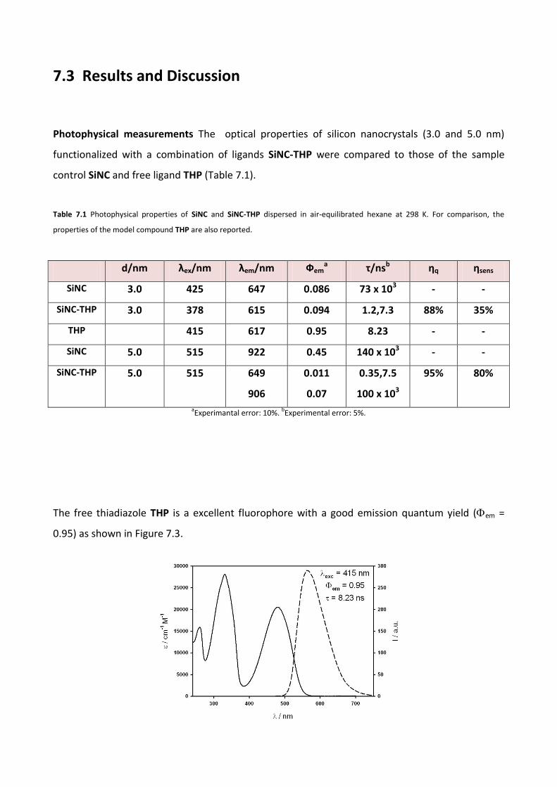
7.3 Results and Discussion
Photophysical measurements The optical properties of silicon nanocrystals (3.0 and 5.0 nm)
functionalized with a combination of ligands SiNC-THP were compared to those of the sample
control SiNC and free ligand THP (Table 7.1).
Table 7.1 Photophysical properties of SiNC and SiNC-THP dispersed in air-equilibrated hexane at 298 K. For comparison, the
properties of the model compound THP are also reported.
d/nm λex/nm λem/nm Фema τ/nsb ηq ηsens
SiNC 3.0 425 647 0.086 73 x 103 - -
SiNC-THP 3.0 378 615 0.094 1.2,7.3 88% 35%
THP 415 617 0.95 8.23 - -
SiNC 5.0 515 922 0.45 140 x 103 - -
SiNC-THP 5.0 515 649
906
0.011
0.07
0.35,7.5
100 x 103
95% 80%
aExperimantal error: 10%.
bExperimental error: 5%.
The free thiadiazole THP is a excellent fluorophore with a good emission quantum yield (em =
0.95) as shown in Figure 7.3.
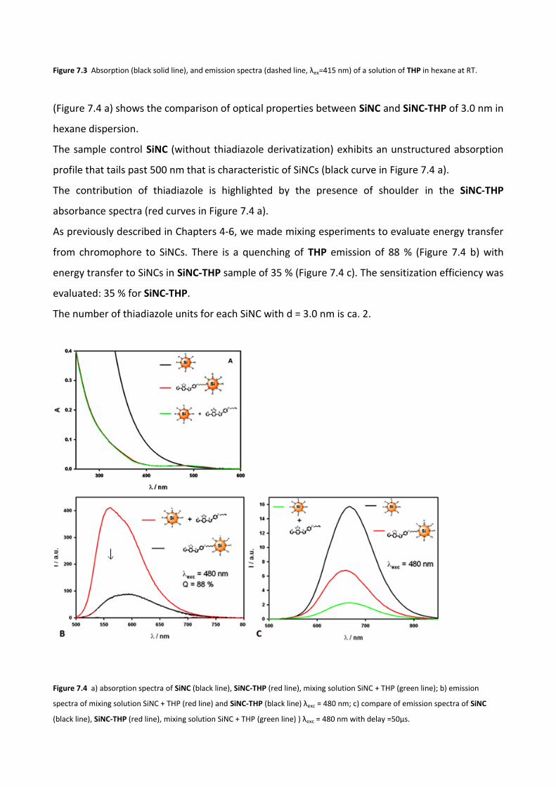
Figure 7.3 Absorption (black solid line), and emission spectra (dashed line, λex=415 nm) of a solution of THP in hexane at RT.
(Figure 7.4 a) shows the comparison of optical properties between SiNC and SiNC-THP of 3.0 nm in
hexane dispersion.
The sample control SiNC (without thiadiazole derivatization) exhibits an unstructured absorption
profile that tails past 500 nm that is characteristic of SiNCs (black curve in Figure 7.4 a).
The contribution of thiadiazole is highlighted by the presence of shoulder in the SiNC-THP
absorbance spectra (red curves in Figure 7.4 a).
As previously described in Chapters 4-6, we made mixing esperiments to evaluate energy transfer
from chromophore to SiNCs. There is a quenching of THP emission of 88 % (Figure 7.4 b) with
energy transfer to SiNCs in SiNC-THP sample of 35 % (Figure 7.4 c). The sensitization efficiency was
evaluated: 35 % for SiNC-THP.
The number of thiadiazole units for each SiNC with d = 3.0 nm is ca. 2.
Figure 7.4 a) absorption spectra of SiNC (black line), SiNC-THP (red line), mixing solution SiNC + THP (green line); b) emission
spectra of mixing solution SiNC + THP (red line) and SiNC-THP (black line) λexc = 480 nm; c) compare of emission spectra of SiNC
(black line), SiNC-THP (red line), mixing solution SiNC + THP (green line) ) λexc = 480 nm with delay =50μs.
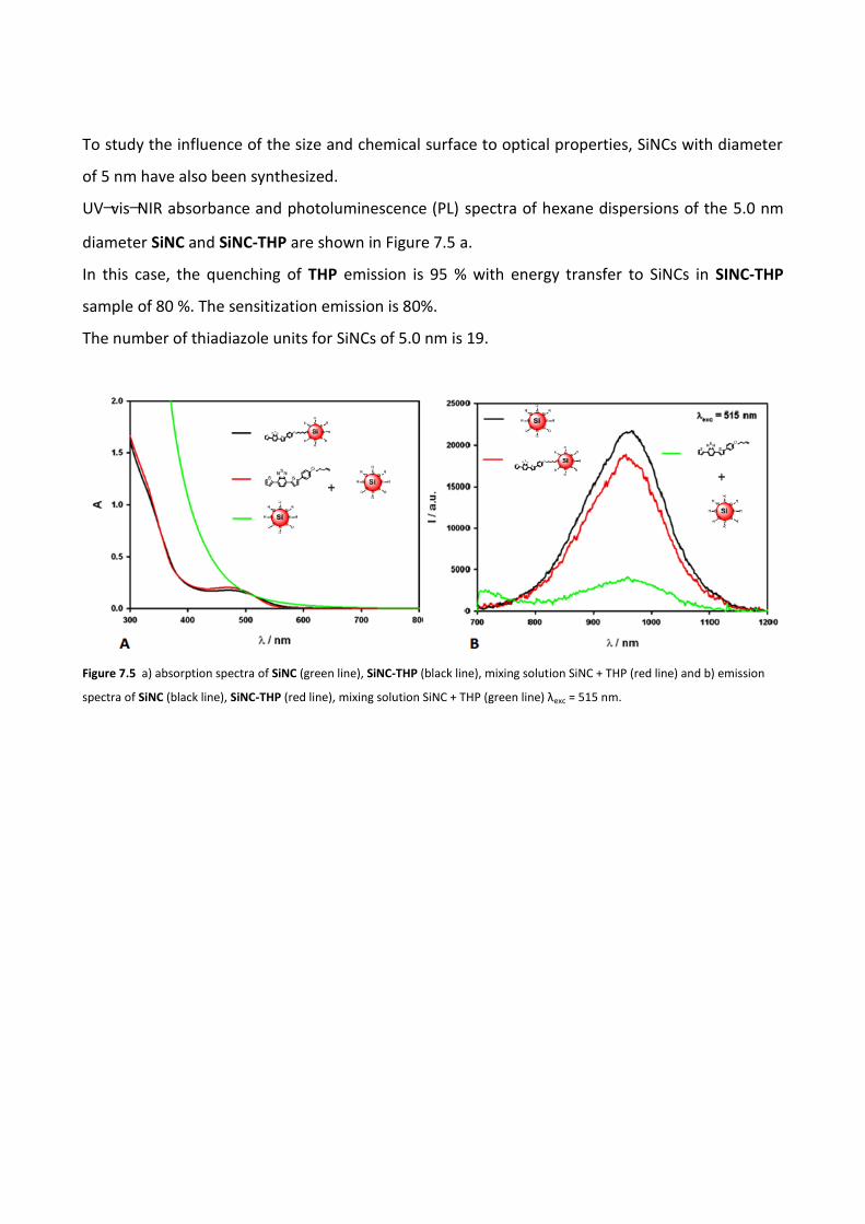
To study the influence of the size and chemical surface to optical properties, SiNCs with diameter
of 5 nm have also been synthesized.
UV−vis−NIR absorbance and photoluminescence (PL) spectra of hexane dispersions of the 5.0 nm
diameter SiNC and SiNC-THP are shown in Figure 7.5 a.
In this case, the quenching of THP emission is 95 % with energy transfer to SiNCs in SINC-THP
sample of 80 %. The sensitization emission is 80%.
The number of thiadiazole units for SiNCs of 5.0 nm is 19.
Figure 7.5 a) absorption spectra of SiNC (green line), SiNC-THP (black line), mixing solution SiNC + THP (red line) and b) emission
spectra of SiNC (black line), SiNC-THP (red line), mixing solution SiNC + THP (green line) λexc = 515 nm.

Perspectives
This thesis has led to the development of a synthetic method that allows to synthesize silicon
nanocrystals with different sizes, narrow size distribution and different chemical properties.
In addition, it has enabled us to achieve a good knowledge of the optical and electronic properties
of semiconductor quantum dots.
The resulting SiNCs posses good optical properties and stability to air.
Nevertheless, it is necessary to improve this method in order to:
- increase the coverage of silicon nanocrystal surface;
- reduce the quantity of ligands used in thermal functionalization;
- find different conditions that enable to use hydrophobic and hydrophilic ligands;
- improve the comprehension of electronic processes.
Furthermore, future work will be dedicated to the post-functionalization of a suitable ligand
attached to the SiNC surface.
The final purpose is to integrate the nanocrystals in multicomponent systems, to build hybrid
materials for the conversion of solar energy into electrical energy.
List of Publications
A. Fermi, M. Baroncini, G. Bergamini, M. Marchini, M. Locritani, P. Ceroni
“A highly luminescent tetramer from a weakly emitting monomer: acid and redox-controlled
multiple complexation by CB [7]”
Chem. Eur. J. 2014, 20, 7054-7060.
E. Marchi, M. Locritani, M. Baroncini, G. Bergamini, R. Sinisi, M. Monari, C. Botta, W. Mroz,
M. Bandini*, P. Ceroni*, V. Balzani
“Blue and highly emitting [Ir(IV)] complexes by an efficient photoreaction of yellow luminescent
[Ir(III)] complexes”
J. Mater. Chem. C, 2014, 2, (22), 4461 – 4467.
M. Locritani, Y. Yu, G. Bergamini, M. Baroncini, J. Molloy, B. A. Korgel*, P. Ceroni*
“Silicon Nanocrystals Functionalized with Pyrene Units: Efficient Light-Harvesting Antennae with
Bright Near-Infrared Emission”
J. Phy. Chem. Lett., 2014, 5, 3325–3329.
American Chemical Society LiveSlides presentation to The Journal of Physical Chemistry
Letters, title: “Silicon Nanocrystals Functionalized with Pyrene Units: Efficient Light
Harvesting Antennae with Bright Near-Infrared Emission” 2014
R. Mazzaro, M. Locritani, J. K. Molloy, M. Montalti, Y. Yu, B. A. Korgel,* G. Bergamini, V. Morandi,*
P. Ceroni*
“Photoinduced processes between pyrene-functionalized Silicon nanocrystals and carbon
allotropes” Submitted


![Quantum Simulations of Out-of-Equilibrium Phenomena · Quantum Simulations of Out-of-Equilibrium Phenomena ... Systeme, z.B. die anisotrope XY Kette, ... explosion [Fey82] of the](https://img.pdfslide.org/doc/110x75/5b9d375d09d3f253158bcf73/quantum-simulations-of-out-of-equilibrium-phenomena-quantum-simulations-of-out-of-equilibrium.jpg)