Embed Size (px)
Citation preview
.
E. Riedle PhysikLMU
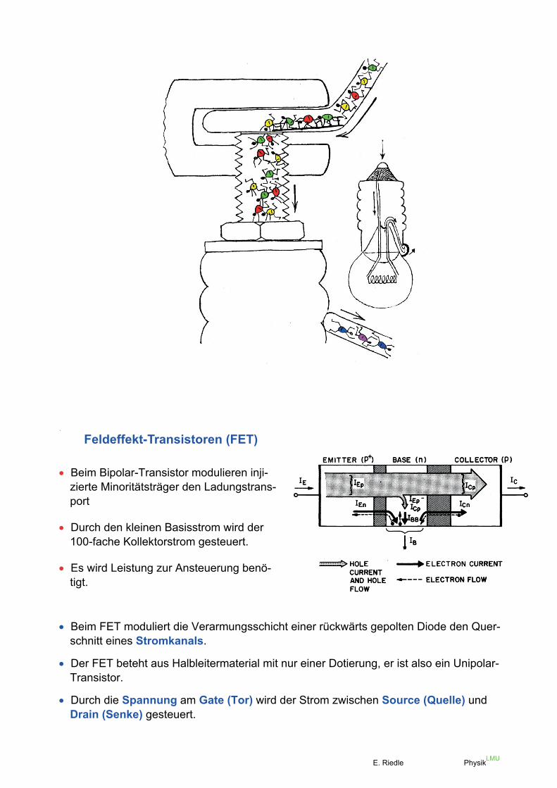
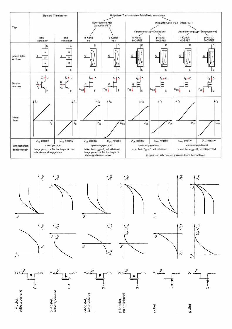
Feldeffekt-Transistoren (FET)
Beim Bipolar-Transistor modulieren inji-zierte Minoritätsträger den Ladungstrans-port
Durch den kleinen Basisstrom wird der 100-fache Kollektorstrom gesteuert.
Es wird Leistung zur Ansteuerung benö-tigt.
Beim FET moduliert die Verarmungsschicht einer rückwärts gepolten Diode den Quer-schnitt eines Stromkanals.
Der FET beteht aus Halbleitermaterial mit nur einer Dotierung, er ist also ein Unipolar-Transistor.
Durch die Spannung am Gate (Tor) wird der Strom zwischen Source (Quelle) und Drain (Senke) gesteuert.
198
ELEKTRONIKELEKTRONIK SS 2001SS 2001 Prof. Dr. Klaus WilleProf. Dr. Klaus Wille
6.2 Unipolare Transistoren(Feldeffekt-Transistoren)
6.2.1 SelbstleitendeSperrschicht-FET
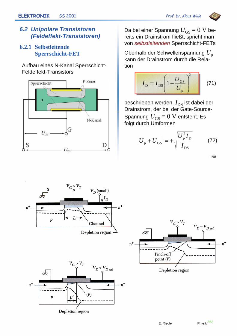
Aufbau eines N-Kanal Sperrschicht-Feldeffekt-Transistors 2
p
GSDSD 1
UUII (71)
Da bei einer Spannung UGS = 0 V be-reits ein Drainstrom fließt, spricht man von selbstleitenden Sperrschicht-FETs
Oberhalb der Schwellenspannung Upkann der Drainstrom durch die Rela-tion
beschrieben werden. IDS ist dabei derDrainstrom, der bei der Gate-Source-Spannung UGS = 0 V entsteht. Esfolgt durch Umformen
DS
D2p
GSp IIU
UU (72)
.
E. Riedle PhysikLMU
199
ELEKTRONIKELEKTRONIK SS 2001SS 2001 Prof. Dr. Klaus WilleProf. Dr. Klaus Wille
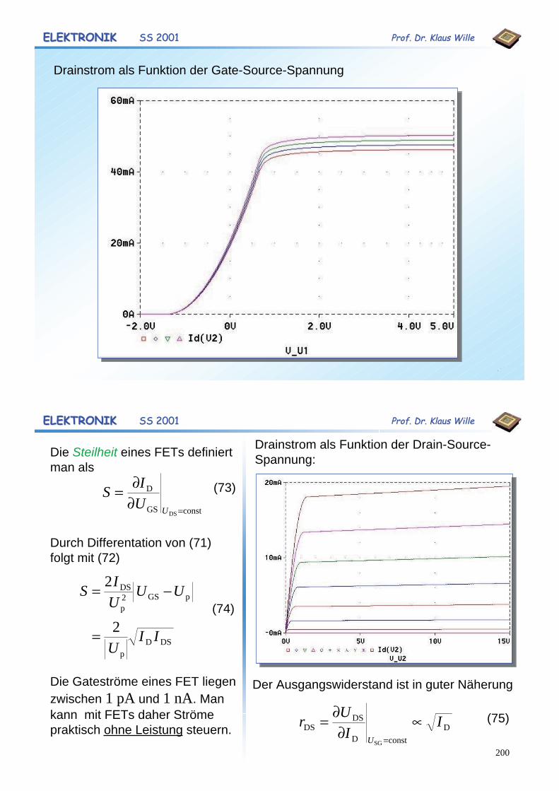
Drainstrom als Funktion der Gate-Source-Spannung
200
ELEKTRONIKELEKTRONIK SS 2001SS 2001 Prof. Dr. Klaus WilleProf. Dr. Klaus Wille
constGS
D
DS
UUIS (73)
DSDp
pGS2p
DS
2
2
IIU
UUUIS
(74)
Die Steilheit eines FETs definiertman als
Durch Differentation von (71)folgt mit (72)
Die Gateströme eines FET liegenzwischen 1 pA und 1 nA. Mankann mit FETs daher Strömepraktisch ohne Leistung steuern. D
constD
DSDS
SG
II
UrU
Drainstrom als Funktion der Drain-Source-Spannung:
Der Ausgangswiderstand ist in guter Näherung
(75)
201
ELEKTRONIKELEKTRONIK SS 2001SS 2001 Prof. Dr. Klaus WilleProf. Dr. Klaus Wille
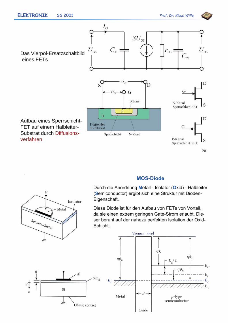
Das Vierpol-Ersatzschaltbild eines FETs
Aufbau eines Sperrschicht-FET auf einem Halbleiter-Substrat durch Diffusions-verfahren
.
E. Riedle PhysikLMU
MOS-Diode Durch die Anordnung Metall - Isolator (Oxid) - Halbleiter (Semiconductor) ergibt sich eine Struktur mit Dioden-Eigenschaft.
Diese Diode ist für den Aufbau von FETs von Vorteil, da sie einen extrem geringen Gate-Strom erlaubt. Die-ser beruht auf der nahezu perfekten Isolation der Oxid-Schicht.
.
E. Riedle PhysikLMU
202
ELEKTRONIKELEKTRONIK SS 2001SS 2001 Prof. Dr. Klaus WilleProf. Dr. Klaus Wille
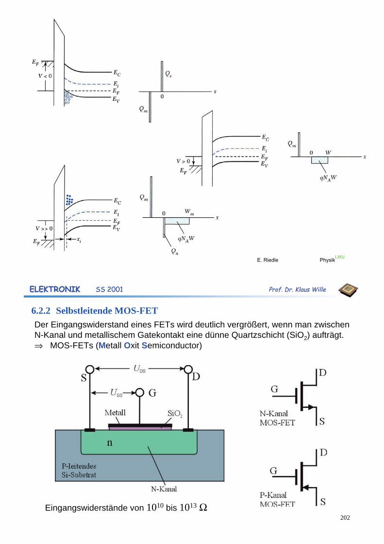
6.2.2 Selbstleitende MOS-FETDer Eingangswiderstand eines FETs wird deutlich vergrößert, wenn man zwischen N-Kanal und metallischem Gatekontakt eine dünne Quartzschicht (SiO2) aufträgt. MOS-FETs (Metall Oxit Semiconductor)
Eingangswiderstände von 1010 bis 1013
203
ELEKTRONIKELEKTRONIK SS 2001SS 2001 Prof. Dr. Klaus WilleProf. Dr. Klaus Wille
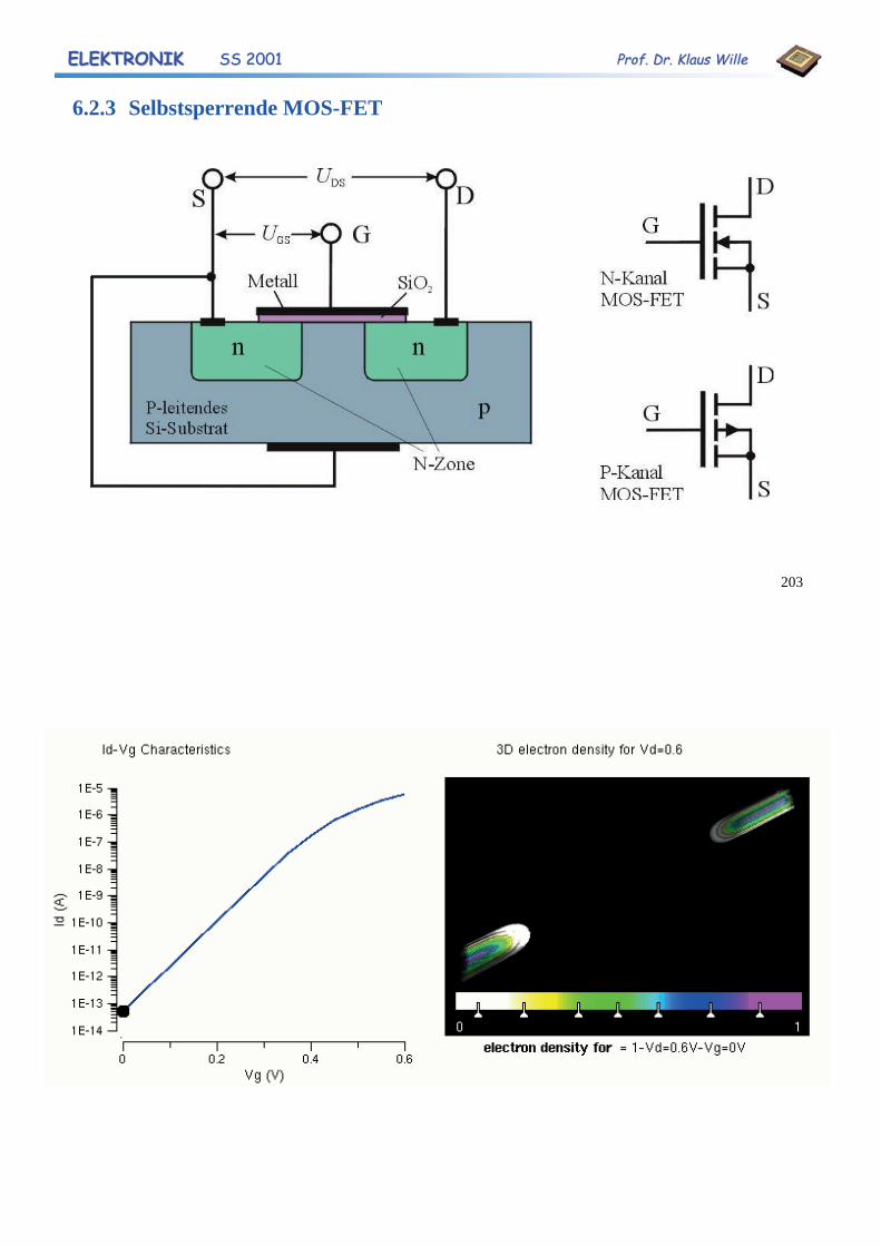
6.2.3 Selbstsperrende MOS-FET
204
ELEKTRONIKELEKTRONIK SS 2001SS 2001 Prof. Dr. Klaus WilleProf. Dr. Klaus Wille
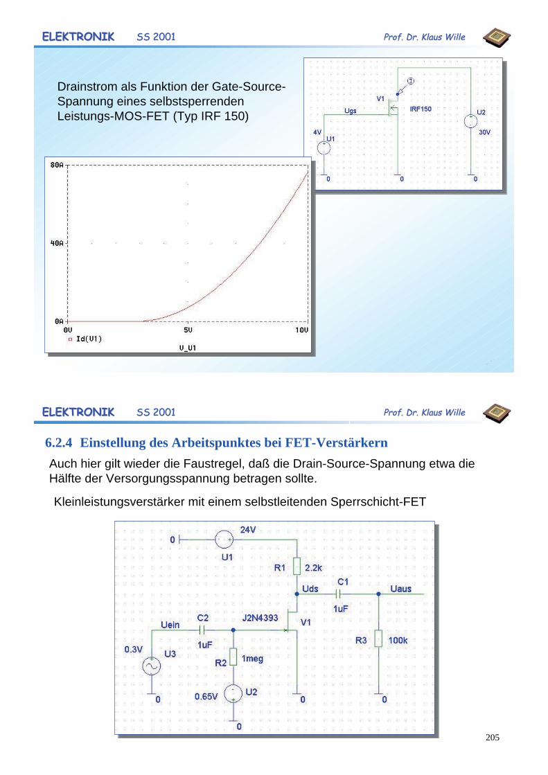
Drainstrom als Funktion der Gate-Source-Spannung eines selbstsperrendenLeistungs-MOS-FET (Typ IRF 150)
205
ELEKTRONIKELEKTRONIK SS 2001SS 2001 Prof. Dr. Klaus WilleProf. Dr. Klaus Wille
6.2.4 Einstellung des Arbeitspunktes bei FET-VerstärkernAuch hier gilt wieder die Faustregel, daß die Drain-Source-Spannung etwa dieHälfte der Versorgungsspannung betragen sollte.
Kleinleistungsverstärker mit einem selbstleitenden Sperrschicht-FET
206
ELEKTRONIKELEKTRONIK SS 2001SS 2001 Prof. Dr. Klaus WilleProf. Dr. Klaus Wille
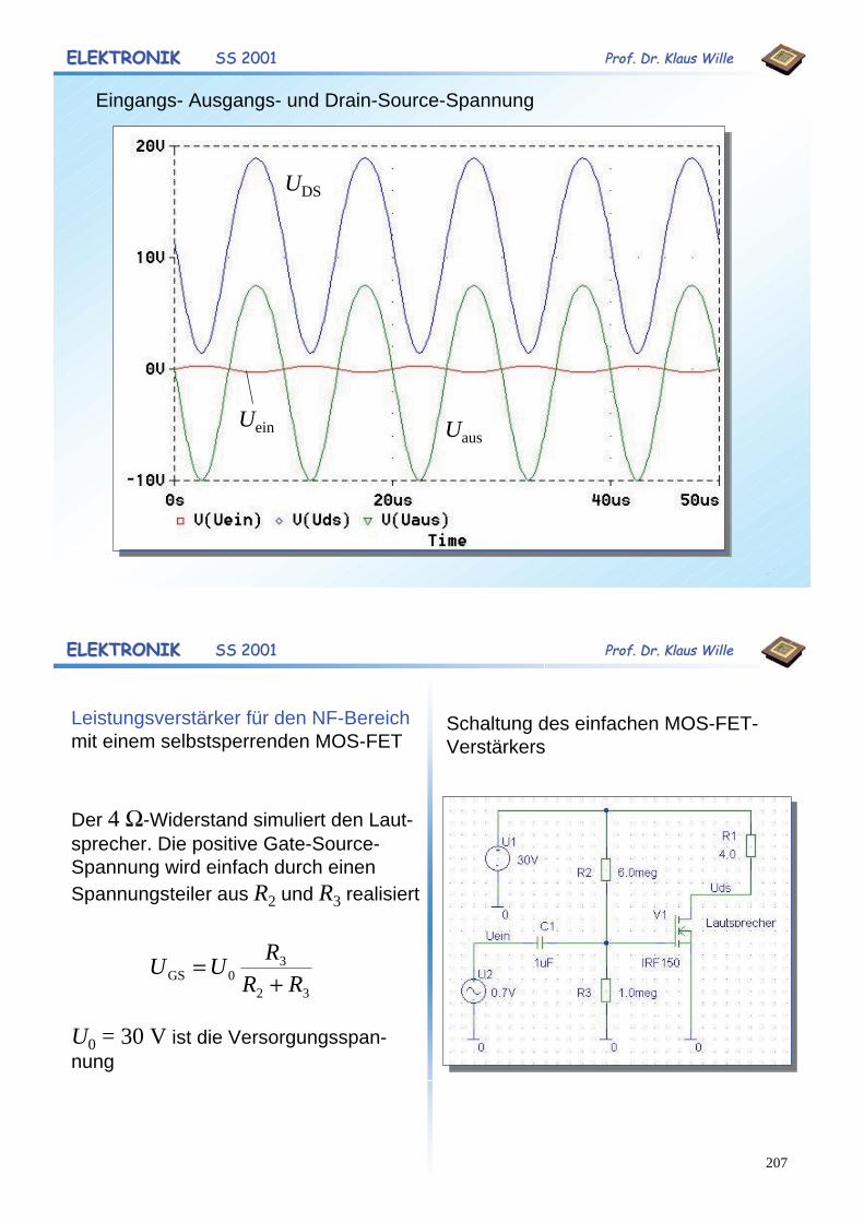
Eingangs- Ausgangs- und Drain-Source-Spannung
UDS
Uein Uaus
207
ELEKTRONIKELEKTRONIK SS 2001SS 2001 Prof. Dr. Klaus WilleProf. Dr. Klaus Wille
32
30GS RR
RUU
Leistungsverstärker für den NF-Bereichmit einem selbstsperrenden MOS-FET
Der 4 -Widerstand simuliert den Laut-sprecher. Die positive Gate-Source-Spannung wird einfach durch einenSpannungsteiler aus R2 und R3 realisiert
Schaltung des einfachen MOS-FET-Verstärkers
U0 = 30 V ist die Versorgungsspan-nung
208
ELEKTRONIKELEKTRONIK SS 2001SS 2001 Prof. Dr. Klaus WilleProf. Dr. Klaus Wille
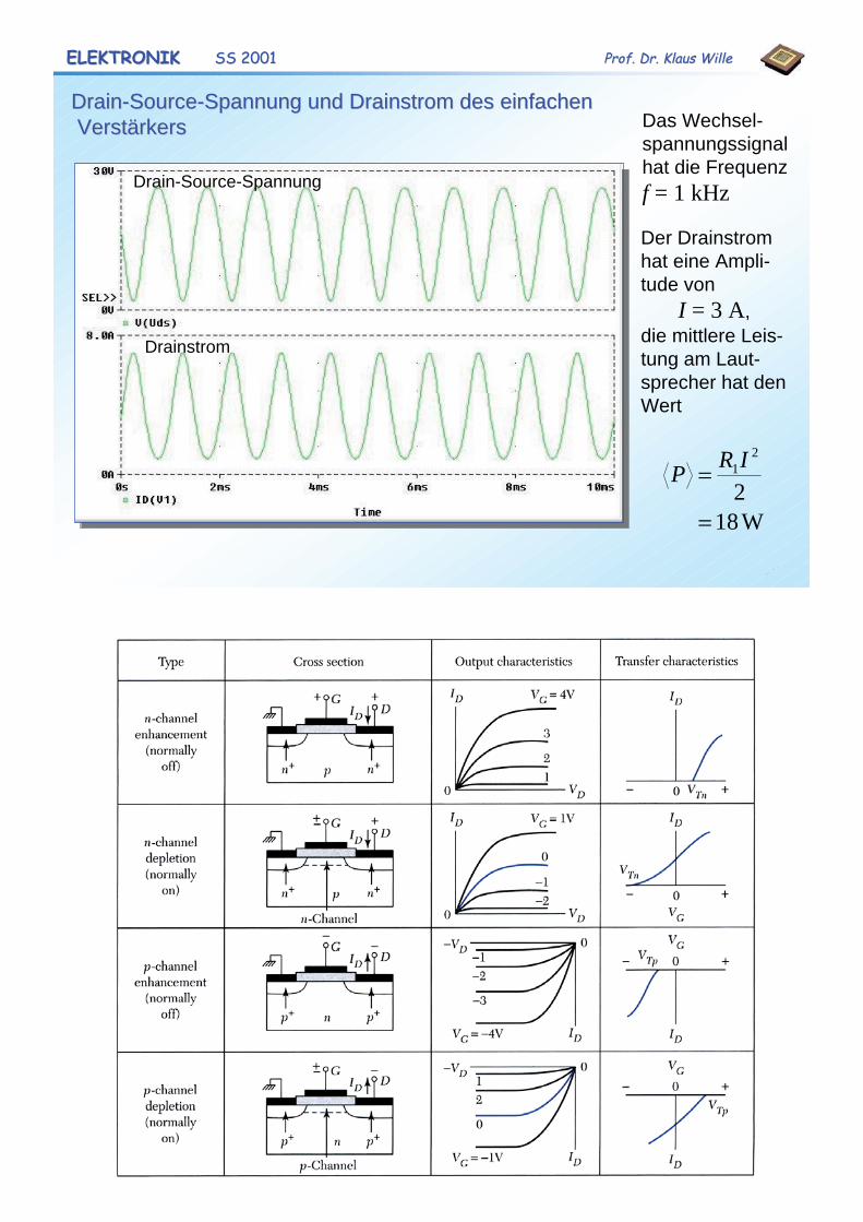
Drain-Source-Spannung
Drainstrom
DrainDrain--SourceSource-Spannung und -Spannung und DrainstromDrainstrom des einfachendes einfachen Verstärkers Verstärkers Das Wechsel-
spannungssignalhat die Frequenzf = 1 kHz
Der Drainstromhat eine Ampli-tude von
I = 3 A,die mittlere Leis-tung am Laut-sprecher hat denWert
W182
21
IRP
Semiconductor
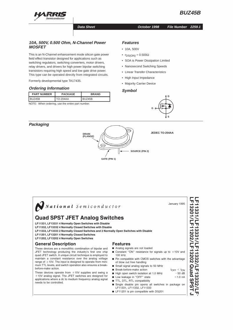
BUZ45B
10A, 500V, 0.500 Ohm, N-Channel PowerMOSFETThis is an N-Channel enhancement mode silicon gate powerfield effect transistor designed for applications such asswitching regulators, switching converters, motor drivers,relay drivers, and drivers for high power bipolar switchingtransistors requiring high speed and low gate drive power.This type can be operated directly from integrated circuits.
Formerly developmental type TA17435.
Features• 10A, 500V
• rDS(ON) = 0.500Ω
• SOA is Power Dissipation Limited
• Nanosecond Switching Speeds
• Linear Transfer Characteristics
• High Input Impedance
• Majority Carrier Device
Symbol
Packaging
JEDEC TO-204AA
Ordering InformationPART NUMBER PACKAGE BRAND
BUZ45B TO-204AA BUZ45B
NOTE: When ordering, use the entire part number.G
D
S
DRAIN(FLANGE)
SOURCE (PIN 2)
GATE (PIN 1)
Data Sheet October 1998 File Number 2259.1
e45
ect
N-nelr-
or
sis-uc--nelr-
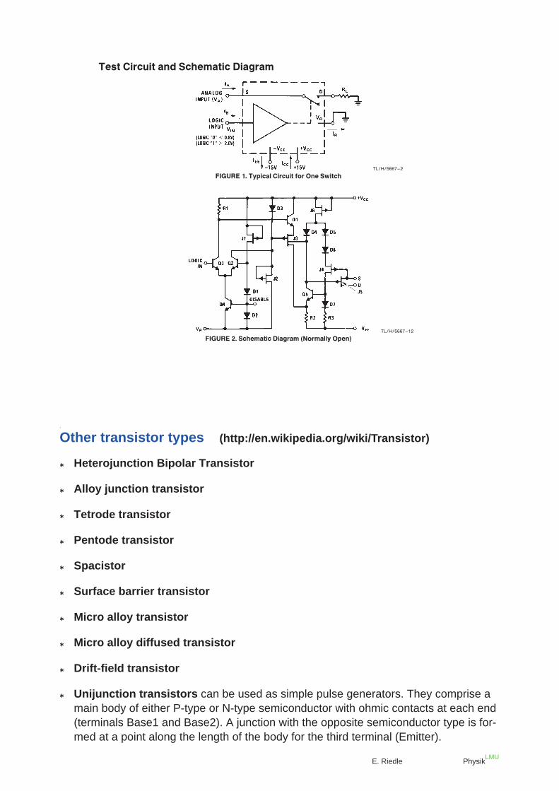
LF11331�LF13331�LF11332�LF13332�LF1
LF13201�LF11202�LF13202
Quad
SPST
JF
January 1995
Quad SPST JFET Analog SwitchesLF11331� LF13331 4 Normally Open Switches with Disable
LF11332� LF13332 4 Normally Closed Switches with Disable
LF11333� LF13333 2 Normally Closed Switches and 2 Normally Open Switches with Disable
LF11201� LF13201 4 Normally Closed Switches
LF11202� LF13202 4 Normally Open Switches
General DescriptionThese devices are a monolithic combination of bipolar and
JFET technology producing the industry’s first one chip
quad JFET switch� A unique circuit technique is employed to
maintain a constant resistance over the analog voltage
range of g10V� The input is designed to operate from mini-
mum TTL levels� and switch operation also ensures a break-
before-make action�
These devices operate from g15V supplies and swing ag10V analog signal� The JFET switches are designed for
applications where a dc to medium frequency analog signal
needs to be controlled�
FeaturesY Analog signals are not loadedY Constant ‘‘ON’’ resistance for signals up to g10V and
100 kHzY Pin compatible with CMOS switches with the advantage
of blow out free handlingY Small signal analog signals to 50 MHzY Break-before-make action tOFF k tONY High open switch isolation at 1�0 MHz b50 dBY Low leakage in ‘‘OFF’’ state k1�0 nAY TTL� DTL� RTL compatibilityY Single disable pin opens all switches in package on
LF11331� LF11332� LF11333Y LF11201 is pin compatible with DG201
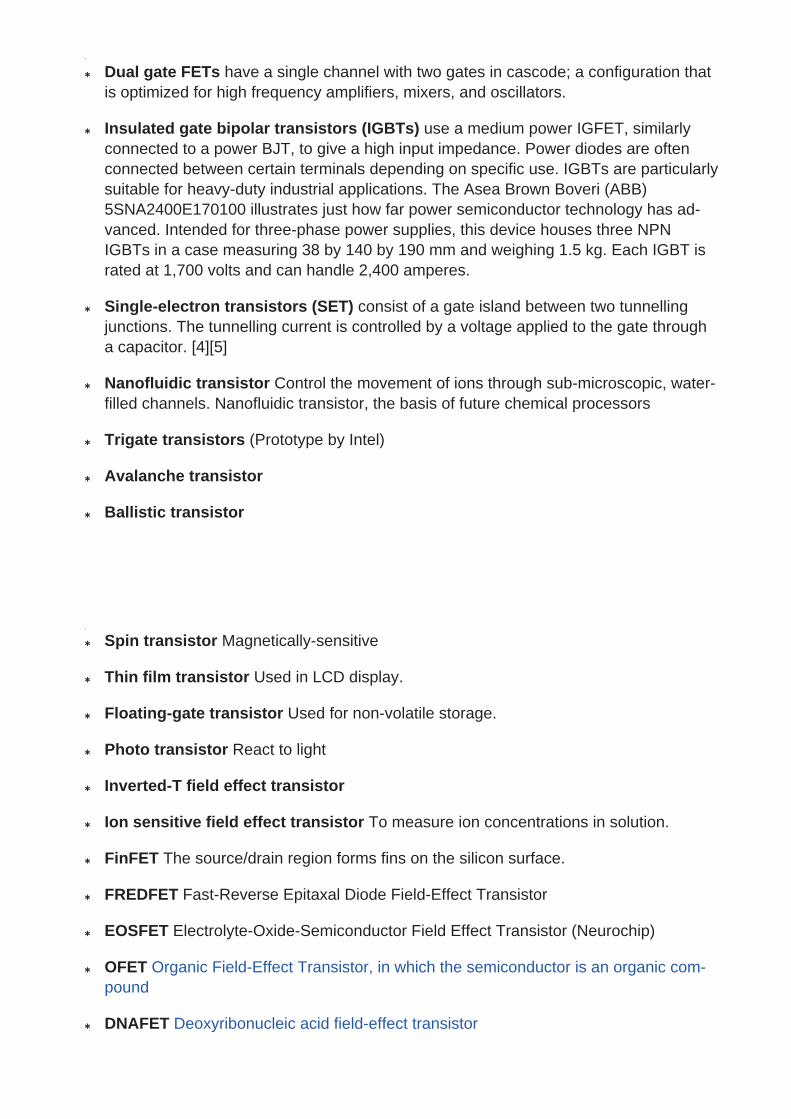
Test Circuit and Schematic Diagram
TL�H�5667–2
FIGURE 1� Typical Circuit for One Switch
TL�H�5667–12
FIGURE 2� Schematic Diagram (Normally Open)
.
E. Riedle PhysikLMU
Other transistor types (http://en.wikipedia.org/wiki/Transistor)
Heterojunction Bipolar Transistor
Alloy junction transistor
Tetrode transistor
Pentode transistor
Spacistor
Surface barrier transistor
Micro alloy transistor
Micro alloy diffused transistor
Drift-field transistor
Unijunction transistors can be used as simple pulse generators. They comprise a main body of either P-type or N-type semiconductor with ohmic contacts at each end (terminals Base1 and Base2). A junction with the opposite semiconductor type is for-med at a point along the length of the body for the third terminal (Emitter).
.
Dual gate FETs have a single channel with two gates in cascode; a configuration that is optimized for high frequency amplifiers, mixers, and oscillators.
Insulated gate bipolar transistors (IGBTs) use a medium power IGFET, similarly connected to a power BJT, to give a high input impedance. Power diodes are often connected between certain terminals depending on specific use. IGBTs are particularly suitable for heavy-duty industrial applications. The Asea Brown Boveri (ABB) 5SNA2400E170100 illustrates just how far power semiconductor technology has ad-vanced. Intended for three-phase power supplies, this device houses three NPN IGBTs in a case measuring 38 by 140 by 190 mm and weighing 1.5 kg. Each IGBT is rated at 1,700 volts and can handle 2,400 amperes.
Single-electron transistors (SET) consist of a gate island between two tunnelling junctions. The tunnelling current is controlled by a voltage applied to the gate through a capacitor. [4][5]
Nanofluidic transistor Control the movement of ions through sub-microscopic, water-filled channels. Nanofluidic transistor, the basis of future chemical processors
Trigate transistors (Prototype by Intel)
Avalanche transistor
Ballistic transistor
.
Spin transistor Magnetically-sensitive
Thin film transistor Used in LCD display.
Floating-gate transistor Used for non-volatile storage.
Photo transistor React to light
Inverted-T field effect transistor
Ion sensitive field effect transistor To measure ion concentrations in solution.
FinFET The source/drain region forms fins on the silicon surface.
FREDFET Fast-Reverse Epitaxal Diode Field-Effect Transistor
EOSFET Electrolyte-Oxide-Semiconductor Field Effect Transistor (Neurochip)
OFET Organic Field-Effect Transistor, in which the semiconductor is an organic com-pound
DNAFET Deoxyribonucleic acid field-effect transistor