Embed Size (px)
Citation preview
Electronic transport properties of electron- and hole-doped semiconducting C1b Heuslercompounds: NiTi1−xMxSn (M=Sc, V)
Siham Ouardi, Gerhard H. Fecher,* Benjamin Balke, Xenia Kozina, Gregory Stryganyuk, and Claudia FelserInstitut für Anorganische und Analytische Chemie, Johannes Gutenberg-Universität, 55099 Mainz, Germany
Stephan Lowitzer, Diemo Ködderitzsch, and Hubert EbertDepartment Chemie, Physikalische Chemie, Ludwig-Maximilians-Universität, 81377 München, Germany
Eiji IkenagaJapan Synchrotron Radiation Research Institute, SPring-8, Hyogo 679-5198, Japan
�Received 20 April 2010; revised manuscript received 17 June 2010; published 11 August 2010�
The substitutional series of Heusler compounds NiTi1−xMxSn �where M =Sc,V and 0�x�0.2� were syn-thesized and investigated with respect to their electronic structure and transport properties. The results showthe possibility to create n-type and p-type thermoelectrics within one Heusler compound. The electronicstructure and transport properties were calculated by all-electron ab initio methods and compared to themeasurements. Hard x-ray photoelectron spectroscopy was carried out and the results are compared to thecalculated electronic structure. Pure NiTiSn exhibits massive “in gap” states containing about 0.1 electrons percell. The comparison of calculations, x-ray diffraction, and photoemission reveals that Ti atoms swapped intothe vacant site are responsible for these states. The carrier concentration and temperature dependence ofelectrical conductivity, Seebeck coefficient, and thermal conductivity were investigated in the range from 10 to300 K. The experimentally determined electronic structure and transport measurements agree well with thecalculations. The sign of the Seebeck coefficient changes from negative for V to positive for Sc substitution.The high n-type and low p-type power factors are explained by differences in the chemical-disorder scattering-induced electric resistivity. Major differences appear because p-type doping �Sc� creates holes in the triplydegenerate valence band at � whereas n-type doping �V� fills electrons in the single conduction band above theindirect gap at X what is typical for all semiconducting transition-metal-based Heusler compounds with C1b
structure.
DOI: 10.1103/PhysRevB.82.085108 PACS number�s�: 31.15.A�, 71.23.�k, 72.15.Jf
I. INTRODUCTION
Heusler compounds are ternary intermetallics consistingof two transition metals and one main group element. TheHeusler compounds with a 1:1:1 composition crystallize in
the cubic MgAgAs-type structure �F4̄3m ,C1b�.1,2 Most ofthose with 18 valence electrons in the primitive cell are ex-pected to be semiconducting.3 They are considered to bepromising thermoelectric materials because of their potentialrole in the realization of environmentally friendly technology�see Ref. 4 for a recent review�.
The compounds of the general formula NiMSn �M=Ti,Zr,Hf� have 18 valence electrons. They were reportedto exhibit unusual transport and optical properties because ofthe band gap or pseudogap at the Fermi energy. Sakuradaand Shutoh5,6 reported a high figure of merit of 1.5 at 700 Kfor Sb-doped NiTi0.50Zr0.25Hf.25Sn, which is one of the high-est values for Heusler compounds at that temperature. A va-riety of substitutions in NiMSn with other main-group metalsas well as transition metals have been made for further opti-mization of the thermoelectric performance.4 For example,doping on the M and Ni sites causes mass fluctuation disor-der that may lead to a reduction in thermal conductivity6–10
while doping on the Sn site provides charge carriers.7,10 Nu-merous Heusler alloys have been investigated focusing ontheir high-temperature thermoelectric properties. The major-ity of these compounds are n-type thermoelectric materials.
On the other hand, efficient p-type materials based on Heu-sler compounds that operate at high temperatures are rare.
In order to achieve the best performance of thermoelectricmodules the n- and p-type materials to be used should bedesigned to exhibit similar chemical and physicalproperties.11 This can be easily realized when starting fromthe same material, here the Heusler compound NiTiSn.Yang12 evaluated theoretically the thermoelectric-relatedelectrical transport properties of several Heusler compounds,they calculated the maximum power factors and the corre-sponding optimal n- or p-type doping levels, which can pro-vide guidance to experimental work. Horyn’ et al.13 investi-gated the effect of a partial substitution of Ti and Zr by Sc onthe thermoelectric properties of NiMSn-based compoundsand obtained at room temperature a fairly high positive See-beck coefficient of about 121 �V /K with 5% Sc substitu-tion of Zr. Miyamoto et al.14 studied the electronic structuresof the Heusler compounds NiMSn by means of photoelec-tron spectroscopy. They observed “in gap” states close to theFermi edge and suggested that these electronic states aremainly created by chemical disorder, which could be the keyto control the thermoelectric properties.
In the commonly used one-parabolic-band approaches n-or p-type doping lead to rather similar results, just with op-posite signs for the Seebeck coefficient. The situation inpractical materials is more difficult. Depleting the valence orfilling the conduction band acts on electronic states with
PHYSICAL REVIEW B 82, 085108 �2010�
1098-0121/2010/82�8�/085108�9� ©2010 The American Physical Society085108-1
rather different characters. It will be shown that the effect ofdoping shows a completely different impact for the NiTiSncompounds when comparing n- and p-type substitutions. Toexplain the different effects on the conductivity a new ap-proach is used that combines the coherent potential approxi-mation and calculation of the impurity-scattering resistivityfor the multielement case. In the present study, the electronicstructure and transport properties of the series NiTi1−xMxSn�where M =Sc,V and 0�x�0.2� were calculated by ab ini-tio methods. The series was synthesized and the structurewas determined by x-ray diffraction �XRD�. The transportproperties were investigated and the results are compared tothe calculated properties. Hard x-ray photoelectron spectros-copy �HAXPES� was performed on the compounds to ex-perimentally determine the valence states and to comparethem to the calculated electronic structure.
II. DETAILS OF THE CALCULATIONS
The electronic structure and transport properties were cal-culated by all-electron ab initio methods. The full-potentiallinearized augmented plane-wave method as implemented inWIEN2k �Ref. 15� in combination with a modified version ofBOLTZTRAP �Ref. 16� has been used for ordered, pure 1:1:1compounds �for details see Refs. 17 and 18�. If not notedotherwise, the exchange-correlation functional was takenwithin the generalized gradient approximation �GGA� in theparametrization of Perdew-Burke-Enzerhof �PBE�.19 A �31�31�31� point mesh was used resulting in 816 k points inthe irreducible wedge of the Brillouin zone. The energy con-vergence criterion was set to 10−5 Ry and simultaneously thecriterion for charge convergence to 10−3e−. The muffin-tinradii were set to 2.4aB for the transition metals and 2.25aBfor the main group element �Bohr’s radius: aB=0.5291772 Å�. For the calculation of the transport proper-ties the tetrahedron method and energy steps of �0.16�10−04 Ry were used for integration. Relaxed lattice param-eters were used in all calculations, the optimization of thevolume resulted in a=5.9534 Å for NiTiSn. Typical for theuse of GGA, this value is slightly larger �0.6%� compared tothe one found from experiments. This is not a critical issue asthe band gap is rather stable against variation in a indepen-dent of the used functional �see below�.
The electronic-structure calculations of the substitution-ally disordered NiTi1−xMxSn �where M =Sc,V and 0�x�0.2� have been performed by means of the fully relativisticKorringa-Kohn-Rostoker �KKR� method in combinationwith the coherent potential approximation �CPA� as imple-mented in the MUNICH-SPRKKR program package.20 Thek-integration mesh was set to a size of �22�22�22� duringthe self-consistent cycles. The gradient correction of the PBEfunctional was switched off for the vacant site to avoid nu-merical instabilities caused by low charge densities.
The CPA allows electronic-structure calculations for sys-tems with random distribution of the atoms as is here thecase where M substitutes partially Ti. For the substitutionalcompounds, the CPA method has been used to model thestatistic distribution of the atoms on the M site and the Tiatoms on a common site of the C1b crystalline structure. The
Ni atoms are placed on the 4a Wyckoff position, the Ti atomsare placed together with the M atoms on the 4c position, andthe main group element Sn is finally placed on the 4d posi-
tion of the cell with F4̄3m symmetry �space group 216�. Theswap-type disordered NiTiSn �for example, Ni1−xVcxTiSn�compound was also treated using the CPA method by placinga fraction of x vacancies �Vc� on regular sites and simulta-neously the swapped part �1−x� on the 4b Wyckoff position.
The conductivity of the compounds with random substi-tution was calculate using the Kubo-Greenwood linear-response formalism as described in Ref. 21 including vertexcorrections.22 The original formulation22 was for the case ofone site per cell and is extended in the present work to in-clude primitive cells with a basis that contains several differ-ent sites. The chemical-disorder scattering resistivity ofNiTi1−xMxSn was calculated using an enlarged �92�92�92� k mesh.
The transport properties discussed in the following de-pend, indeed, critically on the size of the band gap. It is oftennoted that the local-density approximation underestimatesthe band gaps of semiconductors and insulators �for a recentdiscussion see Ref. 23�. Very often, specialized functionals�for example, the Engel-Vosko �EV� GGA functional �Ref.24�� or hybrid functionals including Hartree-Fock exchange�for example, Becke’s B3LYP �Ref. 25�� give better valuesfor the band gaps if applied to sp-element-based semicon-ductors, likewise Ge �0.17 eV with PBE, 0.65 eV with EV,and 0.78 eV in experiments� or GaAs �0.48 eV �PBE�, 1.04eV �EV�, and 1.5 eV �exp��. To check for influences of theexchange-correlation functional, the electronic structure ofNiTiSn was also calculated using the local spin density ap-proximation �LSDA�,26 EV-GGA,24 and the PBEsol �Ref. 27�functionals. Surprisingly, the size of the band gap stayedstable within less than 100 meV without remarkable changesin the band structure. This points to a fundamental differencein the description of d-element-based Heusler semiconduc-tors compared to the sp-element materials. Obviously, theband gap of the d-element semiconductors investigated hereis much less influenced by the choice of the functional ascompared to sp-type semiconductors.
III. EXPERIMENTAL DETAILS
The series NiTi1−xMxSn �M =Sc,V and x=0, . . . ,0.1� wasprepared by arc melting using a mixture of stoichiometricamounts of the elements. To ensure the homogeneity of thesamples they were remelted several times. The as-castsamples were subsequently annealed at 950 °C for 72 h fol-lowed by quenching in ice water in order to improve thecrystalline order. The existence of a single and composition-ally homogeneous phase was verified by x-ray powder dif-fraction using Mo K� radiation. The determination of thelattice parameters and the crystal-structure refinements wereperformed using the Rietveld method.
For the transport measurement bars of �2�2�8� mm3
were cut from the ingots and polished on each side. Themeasurements of the Seebeck coefficient, thermal conductiv-ity, and resistivity were performed by means of a physicalproperties measurement system �Quantum Design Model:
OUARDI et al. PHYSICAL REVIEW B 82, 085108 �2010�
085108-2
6000; supported by LOT, Germany�. The temperature wasvaried from 10 K to room temperature. The measurementswere performed at a residual pressure of about 9.0�10−5 mbar in the chamber.
The HAXPES experiments were performed at the undu-lator beamline BL47XU of SPring-8 �Hyogo, Japan�. Thephoton energy was fixed at 7.9382 keV using a Si�111�double crystal monochromator and a Si�444� channel-cutpostmonochromator. The photoemitted electrons were ana-lyzed for their kinetic energy and detected by a hemispheri-cal analyzer �VG Scienta R4000�. The overall energy reso-lution �monochromator plus analyzer� was set to 250 meV, asverified by low-temperature spectra of the Au valence bandat the Fermi energy ��F�. Additionally, spectra close to theFermi energy were taken with a resolution of 150 meV. Theangle between the electron spectrometer and photon propa-gation is fixed at 90° in all experiments. A near normal emis-sion �=2°� detection angle was used resulting in an angle ofphoton incidence of �=88°. For the HAXPES investigations,the sample bars were fractured in situ. This assures that thesamples are free of oxygen contamination. The measure-ments were taken at sample temperatures of 20 and 300 K.
IV. RESULTS AND DISCUSSION
A. Electronic structure and transport
Figure 1 shows the calculated band structure and the den-sity of states of NiTiSn. The compound is a semiconductorwith an indirect gap. The valence-band maximum appears at� and the conduction-band minimum at X. The band gap hasa size of Egap=0.45 eV. The optical gap at � is consider-ably larger �E�=1.38 eV�.
The electronic structure exhibits at 5–8 eV below theFermi energy the typical sp hybridization gap that separatesthe low-lying a1�s� from the t1�p� bands. The high density ofstates at about −2 eV emerges mainly from Ni d states. Thehigh density of states at −0.7 eV arises mainly from Ni dstates with e symmetry. Most important for the transportproperties, the states at both band edges are due to Ti d stateswith t2 symmetry. From the band structure shown in Fig. 1 itis obvious that electron �n� or hole �p� doping will haverather different results. It is easily seen that p-type dopingcreates holes in the triply degenerate valence band at �
whereas the situation is completely different for n-type dop-ing that fills electrons into the single conduction band abovethe indirect gap at X.
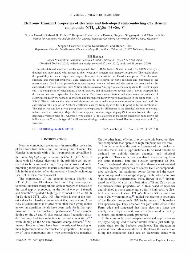
Starting from the calculated electronic structure, the trans-port properties were calculated using Boltzmann transporttheory.28 Doping the semiconducting materials by electronsor holes will change the transport properties. The doping willcause the chemical potential to change its position. At high-doping levels it will shift into the valence �hole doping� orconduction �electron doping� band. Figure 2 shows the cal-culated Seebeck and power coefficients as function of theposition of the chemical potential. The calculations were per-formed for T=300 K. It is assumed that the shift ��=0corresponds to the middle of the band gap at T=0. In Refs.29 and 30 the calculated Boltzmann transport quantities werereported as a function of the chemical potential and tempera-ture for much higher doping level using the same method.The results agree with the here reported values for low dop-ing that close the gap in the considered range of substitution.
The Seebeck coefficient exhibits the typical semiconduc-tor behavior under doping, it is positive for hole and negativefor electron doping. It is largest for small shifts of the chemi-cal potential from the original position. At 300 K it is alreadyslightly positive in the middle of the band gap, the reason isthe shift of the chemical potential with temperature �=��T� to ensure charge neutrality of the system when novoltage is applied. At 300 K the shift amounts to ���13 meV. The size and direction of the shift depend on theshape of the valence and conduction bands.
Figure 3 shows the temperature dependence of the chemi-cal potential and its effect on the Seebeck coefficient of theundoped material. �� was also calculated for low electron orhole doping �10−6 ,10−3� with hypothetical impurity states lo-
FIG. 1. Electronic structure of NiTiSn.
FIG. 2. Calculated Seebeck and power coefficients of NiTiSn.The shift of the chemical potential is given with respect to the sizeof the gap. The valence and conduction band extrema are markedby dashed lines �T=300 K�.
ELECTRONIC TRANSPORT PROPERTIES OF ELECTRON-… PHYSICAL REVIEW B 82, 085108 �2010�
085108-3
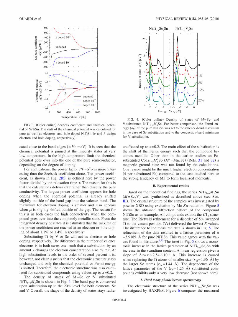
cated close to the band edges ��50 meV�. It is seen that thechemical potential is pinned at the impurity states at verylow temperature. In the high-temperature limit the chemicalpotential goes over into the one of the pure semiconductor,depending on the degree of doping.
For applications, the power factor PF=S2 is more inter-esting than the Seebeck coefficient alone. The power coeffi-cient, as shown in Fig. 2�b�, is defined here by the powerfactor divided by the relaxation time �. The reason for this isthat the calculations deliver /� rather than directly the pureconductivity. The largest power coefficient appears for holedoping when the chemical potential is already shiftedslightly outside of the band gap into the valence band. Themaximum for electron doping is smaller and also appearswhen � is slightly shifted outside of the gap. The reason forthis is in both cases the high conductivity when the com-pound goes over into the completely metallic state. From theintegrated density of states it is estimated that the maxima ofthe power coefficient are reached at an electron or hole dop-ing of about 1.1% or 1.4%, respectively.
Substituting Ti by V or Sc will act as electron or holedoping, respectively. The difference in the number of valenceelectrons is in both cases one, such that a substitution by anamount x changes the electron concentration also by �x. Athigh substitution levels in the order of several percent it is,however, not clear a priori that the electronic structure staysunchanged and only the chemical potential or Fermi energyis shifted. Therefore, the electronic structure was also calcu-lated for substituted compounds using values up to x=0.2.
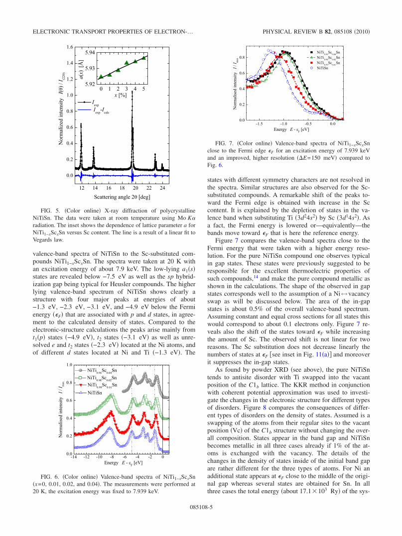
The density of states of M =Sc or V substitutedNiTi1−xMxSn is shown in Fig. 4. The band gap is conservedupon substitution up to the 20% level for both elements, Scand V. Overall, the shape of the density of states stays rather
unaffected up to x=0.2. The main effect of the substitution isthe shift of the Fermi energy such that the compound be-comes metallic. Other than in the earlier studies on Fe-substituted CoTi1−xMx�Sb �M�=Mn,Fe� �Refs. 31 and 32� amagnetic ground state was not found by the calculations.One reason might be the much higher electron concentration�4 per substituted Fe� compared to the case studied here orthe strong tendency of Mn to form localized moments.
B. Experimental results
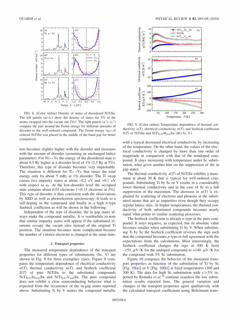
Based on the theoretical findings, the series NiTi1−xMxSn�M =Sc,V� was synthesized as described above �see Sec.III�. The crystal structure of the samples was investigated bypowder XRD using excitation by Mo K� radiation. Figure 5shows the obtained diffraction pattern of the compoundNiTiSn as an example. All compounds exhibit the C1b struc-ture. The Rietveld refinement for a disorder of 5% swappedTi to the vacant position �Vc� delivered the lowest R values.The difference to the measured data is shown in Fig. 5. Therefinement of the data resulted in a lattice parameter of a=5.9185 Å for pure NiTiSn. This value agrees with the val-ues found in literature.6,33 The inset in Fig. 5 shows a mono-tonic increase in the lattice parameter of NiTi1−xScxSn withincrease in the scandium content. A linear regression gives aslope of a=x�2.54�10−3 Å. This increase is causedwhen replacing the Ti atoms of smaller size �rTi=1.36 Å� bythe larger Sc atoms �rSc=1.44 Å�. The dependence of thelattice parameter of the V �rV=1.25 Å� substituted com-pounds exhibits only a very low decrease �not shown here�.
1. Hard x-ray photoelectron spectroscopy
The electronic structure of the series NiTi1−xScxSn wasinvestigated by HAXPES. Figure 6 compares the measured
FIG. 3. �Color online� Seebeck coefficient and chemical poten-tial of NiTiSn. The shift of the chemical potential was calculated forpure as well as electron- and hole-doped NiTiSn �e and h assignelectron and hole doping, respectively�.
FIG. 4. �Color online� Density of states of M =Sc- andV-substituted NiTi1−xMxSn. For better comparison, the Fermi en-ergy ��F� of the pure NiTiSn was set to the valence-band maximumin the case of Sc substitution and to the conduction-band minimumfor V substitution.
OUARDI et al. PHYSICAL REVIEW B 82, 085108 �2010�
085108-4
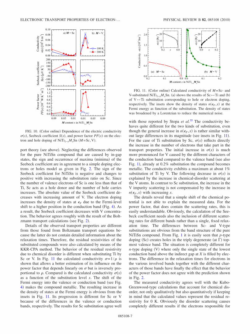
valence-band spectra of NiTiSn to the Sc-substituted com-pounds NiTi1−xScxSn. The spectra were taken at 20 K withan excitation energy of about 7.9 keV. The low-lying a1�s�states are revealed below −7.5 eV as well as the sp hybrid-ization gap being typical for Heusler compounds. The higherlying valence-band spectrum of NiTiSn shows clearly astructure with four major peaks at energies of about−1.3 eV, −2.3 eV, −3.1 eV, and −4.9 eV below the Fermienergy ��F� that are associated with p and d states, in agree-ment to the calculated density of states. Compared to theelectronic-structure calculations the peaks arise mainly fromt1�p� states �−4.9 eV�, t2 states �−3.1 eV� as well as unre-solved e and t2 states �−2.3 eV� located at the Ni atoms, andof different d states located at Ni and Ti �−1.3 eV�. The
states with different symmetry characters are not resolved inthe spectra. Similar structures are also observed for the Sc-substituted compounds. A remarkable shift of the peaks to-ward the Fermi edge is obtained with increase in the Sccontent. It is explained by the depletion of states in the va-lence band when substituting Ti �3d24s2� by Sc �3d14s2�. Asa fact, the Fermi energy is lowered or—equivalently—thebands move toward �F that is here the reference energy.
Figure 7 compares the valence-band spectra close to theFermi energy that were taken with a higher energy reso-lution. For the pure NiTiSn compound one observes typicalin gap states. These states were previously suggested to beresponsible for the excellent thermoelectric properties ofsuch compounds,14 and make the pure compound metallic asshown in the calculations. The shape of the observed in gapstates corresponds well to the assumption of a Ni↔vacancyswap as will be discussed below. The area of the in-gapstates is about 0.5% of the overall valence-band spectrum.Assuming constant and equal cross sections for all states thiswould correspond to about 0.1 electrons only. Figure 7 re-veals also the shift of the states toward �F while increasingthe amount of Sc. The observed shift is not linear for tworeasons. The Sc substitution does not decrease linearly thenumbers of states at �F �see inset in Fig. 11�a�� and moreoverit suppresses the in-gap states.
As found by powder XRD �see above�, the pure NiTiSntends to antisite disorder with Ti swapped into the vacantposition of the C1b lattice. The KKR method in conjunctionwith coherent potential approximation was used to investi-gate the changes in the electronic structure for different typesof disorders. Figure 8 compares the consequences of differ-ent types of disorders on the density of states. Assumed is aswapping of the atoms from their regular sites to the vacantposition �Vc� of the C1b structure without changing the over-all composition. States appear in the band gap and NiTiSnbecomes metallic in all three cases already if 1% of the at-oms is exchanged with the vacancy. The details of thechanges in the density of states inside of the initial band gapare rather different for the three types of atoms. For Ni anadditional state appears at �F close to the middle of the origi-nal gap whereas several states are obtained for Sn. In allthree cases the total energy �about 17.1�103 Ry� of the sys-
FIG. 5. �Color online� X-ray diffraction of polycrystallineNiTiSn. The data were taken at room temperature using Mo K�radiation. The inset shows the dependence of lattice parameter a forNiTi1−xScxSn versus Sc content. The line is a result of a linear fit toVegards law.
FIG. 6. �Color online� Valence-band spectra of NiTi1−xScxSn�x=0, 0.01, 0.02, and 0.04�. The measurements were performed at20 K, the excitation energy was fixed to 7.939 keV.
FIG. 7. �Color online� Valence-band spectra of NiTi1−xScxSnclose to the Fermi edge �F for an excitation energy of 7.939 keVand an improved, higher resolution �E=150 meV� compared toFig. 6.
ELECTRONIC TRANSPORT PROPERTIES OF ELECTRON-… PHYSICAL REVIEW B 82, 085108 �2010�
085108-5
tem becomes slightly higher with the disorder and increaseswith the amount of disorder �assuming an unchanged latticeparameter�. For Ni↔Vc the energy of the disordered state isabout 0.5 Ry higher at a disorder level of 1% �2.5 Ry at 5%�.Therefore, this type of disorder becomes very improbable.The situation is different for Ti↔Vc that raises the totalenergy only by about 5 mRy at 1% disorder. The Ti swapcauses two impurity states at about −0.2 eV and +0.1 eVwith respect to �F. At the low-disorder level the occupiedstate contains about 0.03 electrons ��0.15 electrons at 5%�.This type of disorder is thus consistent with the observationsby XRD as well as photoelectron spectroscopy. It leads to aself-doping in the compound and finally in a high n-typeSeebeck coefficient as will be shown in the following.
Independent of the type of disorder, the in gap states al-ways make the compound metallic. It is worthwhile to notethat similar impurity states will appear if the substituted el-ements occupy the vacant sites instead of the original Tiposition. The situation becomes more complicated becausethe number of valence electrons is changed at the same time.
2. Transport properties
The measured temperature dependence of the transportproperties for different types of substitutions �Sc, V� areshown in Fig. 9 for three exemplary cases. Figure 9 com-pares the temperature dependence of electrical conductivity �T�, thermal conductivity ��T�, and Seebeck coefficientS�T� of pure NiTiSn to the substituted compoundsNiTi0.97Sc0.03Sn and NiTi0.97V0.03Sn. The pure compounddoes not exhibit a clear semiconducting behavior what isexpected from the occurrence of the in-gap states reportedabove. Substituting Ti by V makes the compound metallic
with a typical decreased electrical conductivity by increasingof the temperature. On the other hand, the values of the elec-trical conductivity is changed by more than one order ofmagnitude in comparison with that of the nondoped com-pound. It stays increasing with temperature under Sc substi-tution, what gives another hint on the suppression of the ingap states.
The thermal conductivity ��T� of NiTiSn exhibits a maxi-mum at about 30 K that is typical for well-ordered com-pounds. Substituting Ti by Sc or V results in a considerablylower thermal conductivity and in the case of Sc to a fullsuppression of the maximum. The decrease in ��T� is ex-plained by scattering of electrons and phonons at the substi-tuted atoms that act as impurities even though they occupyregular lattice sites. At higher temperatures, the thermal con-ductivity of both substituted compounds becomes nearlyequal what points to similar scattering processes.
The Seebeck coefficient is already n type in the pure com-pound. It stays negative, as expected, but its absolute valuebecomes smaller when substituting Ti by V. When substitut-ing Ti by Sc the Seebeck coefficient reverses the sign suchthat the compound becomes p type in full agreement with theexpectations from the calculations. Most interestingly, theSeebeck coefficient changes the sign at 300 K from−155 �V /K for the undoped compound to +140 �V /K forthe compound with 3% Sc substitution.
Figure 10 compares the behavior of the measured trans-port properties as function of the substitution of Ti by Sc�Fig. 10�a�� or V �Fig. 10�b�� at fixed temperatures �100 and300 K�. The data for high Sc substitution with x�5% re-ported by Romaka et al.34 continue seamless the low substi-tution results reported here. The general variation andchanges in the transport properties agree qualitatively withthe calculated transport coefficients using Boltzmann trans-
FIG. 8. �Color online� Density of states of disordered NiTiSn.The left panels �a�–�c� show the density of states for 5% of theatoms swapped into the vacant site �Vc�. The right panels �a��– �c��compare the part around the Fermi energy for different amounts ofdisorder to the well-ordered compound. The Fermi energy ��F� ofordered NiTiSn was placed in the middle of the band gap for bettercomparison.
FIG. 9. �Color online� Temperature dependence of thermal con-ductivity ��T�, electrical conductivity �T�, and Seebeck coefficientS�T� of NiTiSn and NiTi0.97M0.03Sn �M =Sc,V�.
OUARDI et al. PHYSICAL REVIEW B 82, 085108 �2010�
085108-6
port theory �see above�. Neglecting the differences observedfor the pure NiTiSn compound that are caused by in-gapstates, the sign and occurrence of maxima �minima� of theSeebeck coefficient are in agreement to a simple doping elec-trons or holes model as given in Fig. 2. The sign of theSeebeck coefficient for NiTiSn is negative and changes topositive with increasing the substitution ratio on Sc. Sincethe number of valence electrons of Sc is one less than that ofTi, Sc acts as a hole donor and the number of hole carriesincreases. The absolute value of the Seebeck coefficient de-creases with increasing amount of V. The electron dopingincreases the density of states at �F due to the Fermi-levelshift to a higher position in the conduction band �Fig. 4�. Asa result, the Seebeck coefficient decreases with V concentra-tion. The behavior agrees roughly with the result of the Bolt-zmann transport calculations �see Fig. 2�.
Details of the observed transport properties are differentfrom those found from Boltzmann transport equations be-cause the latter do not contain detailed information about therelaxation times. Therefore, the residual resistivities of thesubstituted compounds were also calculated by means of theKKR-CPA method. The behavior of the residual resistivitydue to chemical disorder is different when substituting Ti bySc or V. In Fig. 11 the calculated conductivity =1 /� isshown that allows a better estimation of its influence on thepower factor that depends linearly on but is inversely pro-portional to �. Compared is the calculated conductivity �x�as a function of the substitution level x. The shift of theFermi energy into the valence or conduction band �see Fig.4� makes the compound metallic. The resulting increase inthe density of states at the Fermi energy is obvious from theinsets in Fig. 11. Its progression is different for Sc or Vbecause of the differences in the valence or conductionbands, respectively. The results for Sc substitution agree well
with those reported by Stopa et al.35 The conductivity be-haves quite different for the two kinds of substitution, eventhough the general increase in n��F ,x� is rather similar with-out large differences in its magnitude �see insets in Fig. 11�.For the case of Ti substitution by Sc, �x� reflects directlythe increase in the number of electrons that take part in thetransport properties. The initial increase in �x� is muchmore pronounced for V caused by the different characters ofthe conduction band compared to the valence band �see alsoFig. 1�, already at 0.2% substitution the compound becomesmetallic. The conductivity exhibits a maximum at about 1%substitution of Ti by V. The following decrease in �x� isexplained by the increase in chemical-disorder scattering atthe V atoms. In contrast to Sc substitution, the increase in theV impurity scattering is not compensated by the increase inn��F ,x� with increasing x.
The details reveal that a simple shift of the chemical po-tential is not able to explain the measured data. For thepower factor, that does contain the scattering rates, this iseasily understandable. Obviously, the calculation of the See-beck coefficient needs also the inclusion of different scatter-ing rates for different bands rather than a single, fixed relax-ation time. The differences between Sc- and V-typesubstitutions are obvious from the band structure of the pureNiTiSn compound. From Fig. 1 it is easily seen that p-typedoping �Sc� creates holes in the triply degenerate �at �� top-most valence band. The situation is completely different forn-type doping �V� where only the single state of the lowestconduction band above the indirect gap at X is filled by elec-trons. The difference in the relaxation times for electrons inthe various involved bands together with the different char-acters of those bands have finally the effect that the behaviorof the power factor does not agree with the prediction shownin Fig. 2.
The measured conductivity agrees well with the Kubo-Greenwood-type calculations that account for chemical dis-order, not only qualitatively but also quantitatively if keepingin mind that the calculated values represent the residual re-sistivity for 0 K. Obviously the disorder scattering causescompletely different results if the electrons responsible for
FIG. 10. �Color online� Dependence of the electric conductivity �x�, Seebeck coefficient S�x�, and power factor PF�x� on the elec-tron and hole doping of NiTi1−xMxSn �M =Sc,V�.
FIG. 11. �Color online� Calculated conductivity of M =Sc- andV-substituted NiTi1−xMxSn. �a� shows the results of Sc↔Ti and �b�of V↔Ti substitution corresponding to hole or electron doping,respectively. The insets show the density of states n��F ,x� at theFermi energy as function of the substitution. The density of stateswas broadened by a Lorentzian to reduce the numerical noise.
ELECTRONIC TRANSPORT PROPERTIES OF ELECTRON-… PHYSICAL REVIEW B 82, 085108 �2010�
085108-7
the transport are from the “initial valence” band for Sc sub-stitution or the “initial conduction” band for V substitution.The behavior of the conductivity has a major impact on thebehavior of the power factor under substitution. The highestvalue is observed for the n-type V substitution and the p-typeSc substitution leads to considerably lower power factors.Indeed, the difference arises from the different behavior ofthe conductivity for both types of substitutions. It is worth-while to note that the rather comparable impact of the sub-stitution on the thermal conductivity favors a high figure ofmerit for the n-type material. According to this observation,the improvement of p-type materials needs essentially an im-provement of their electric conductivity and thus of theirpower factor.
V. SUMMARY
The solid-solution series NiTi1−xMxSn �M =Sc,V� wassystematically studied by experimental and theoretical meth-ods. The electronic structure and transport properties of thecompounds were measured in detail and compared to all-electron ab initio density-functional calculations. The resultsshow the possibility to create n-type and p-type thermoelec-tric materials within one compound series.
X-ray powder diffraction was performed to determine thestructure type and the lattice parameters of the compounds.All compounds of the series crystallize in the C1b structuretype. Substitution of Ti by V or Sc leads to a linear change inthe lattice parameter according to Vegards law. A swap ofabout 5% Ti into the vacant site was found from the diffrac-tion data of pure NiTiSn. Calculations as well as photoelec-tron spectroscopy revealed that this type of antisite disorderis responsible for the occurrence of in gap states that result inthe favorable thermoelectric properties of the pure com-pound.
The thermal conductivity, electrical resistivity, and See-beck coefficient were measured in the temperature rangefrom 10 to 300 K. In general the change in measured trans-port properties with composition agree qualitatively with thecalculations. The n-type behavior of the pure compound isprovided by the in gap states. Sc substitution of Ti leads to ap-type behavior and a suppression of the in gap states. Theobserved behavior of the resistivity of both types of substi-tuted materials is explained by the calculations respectingdisorder scattering. The lattice thermal conductivity of theNiTi1−xMxSn �M =Sc,V� compounds are effectively de-pressed by substitution of Ti by Sc or V. The sign of the
Seebeck coefficient with Sc substitution from n to p type isrelated to the appearance and the dominant contribution offree holes to the intermetallic semiconductor conductivity. Inaddition, the electronic structure of the compounds was stud-ied using bulk sensitive, hard x-ray photoelectron spectros-copy. The observed in gap states suggested that the electronicstates close to the Fermi edge play a key role to control thethermoelectric properties. The observed shifts of the valencestates agree with the calculated shift of the Fermi energywhen substituting Ti by Sc or V.
The reduction in the thermal conductivity is achieved bysubstitution of Ti and independent of the type of the doping�Sc or V�. Therefore, the impact of the lowered thermal con-ductivity on the figure of merit is nearly the same. In order tocreate high efficient thermoelectric materials, it is necessarynot only to improve the figure of merit but also to achieve ahigh power factor. The power factors found in calculationand experiment reveal clearly a different behavior for bothtypes of substitutions. Different from n-type substitution,which exhibits the highest power factor, the p type still hasrather low values. This difference is caused by the differentbehavior of the conductivity when the carriers are from ei-ther the valence or the conduction band. The major distinc-tion appears through the fact that p-type doping �Sc� createsholes in the triply degenerate valence band at � whereasn-type doping �V� fills electrons in the single conductionband above the indirect gap at X. This behavior is typical forthe semiconducting transition-metal-based Heusler com-pounds with C1b structure that all exhibit similar band struc-tures rather independent of the composition.
Respectively, the open challenge to theory and experimentis to find new concepts that depress the thermal conductivityand, at the same time, improve the conductivity at low p-typedoping of Heusler compounds. The presented systematicstudy of the solid-solution series NiTi1−xMxSn �M =Sc,V�shows the possibility to create n-type and p-type thermoelec-tric materials within one compound series.
ACKNOWLEDGMENTS
The authors gratefully acknowledge financial support bythe Deutsche Forschungsgemeinschaft �Project No. FE 633/8-1� and Stiftung Rheinland Pfalz für Innovation �Project863�. The synchrotron radiation HAXPES measurementwere performed at BL47XU with the approval of the JapanSynchrotron Radiation Research Institute �JASRI� �Long-term Proposal No. 2008B0017�.
*[email protected] W. Jeitschko, Metall. Mater. Trans. B 1, 3159 �1970�.2 H. C. Kandpal, C. Felser, and R. Seshadri, J. Phys. D 39, 776
�2006�.3 J. Tobola and J. Pierre, J. Alloys Compd. 296, 243 �2000�.4 J. R. Sootsman, D. Y. Chung, and M. G. Kanatzidis, Angew.
Chem. 48, 8616 �2009�.
5 S. Sakurada and N. Shutoh, Appl. Phys. Lett. 86, 082105�2005�.
6 N. Shutoh and S. Sakurada, J. Alloys Compd. 389, 204 �2005�.7 S. Katsuyama, R. Matsuo, and M. Ito, J. Alloys Compd. 428,
262 �2007�.8 T. Katayama, S. W. Kim, Y. Kimura, and Y. Mishima, J. Elec-
tron. Mater. 32, 1160 �2003�.
OUARDI et al. PHYSICAL REVIEW B 82, 085108 �2010�
085108-8
9 Q. Shen, L. Chen, T. Goto, T. Hirai, J. Yang, G. P. Meisner, andC. Uher, Appl. Phys. Lett. 79, 4165 �2001�.
10 J. Yang, G. P. Meisner, and L. Chen, Appl. Phys. Lett. 85, 1140�2004�.
11 D. Rowe, Thermoelectrics Handbook: Macro to Nano �CRCTaylor & Francis, Boca Raton, 2006�.
12 J. Yang, Adv. Funct. Mater. 18, 2880 �2008�.13 A. Horyn’, O. Bodak, L. Romaka, Y. Gorelenko, A. Tkachuk, V.
Davydov, and Y. Stadnyk, J. Alloys Compd. 363, 10 �2004�.14 K. Miyamoto, K. Kimura, K. Sakamoto, M. Ye, Y. Cui, K. Shi-
mada, H. Namatame, M. Taniguchi, S. I. Fujimori, Y. Saitoh, E.Ikenaga, K. Kobayashi, J. Tadano, and T. Kanomata, Appl. Phys.Express 1, 081901 �2008�.
15 P. Blaha, K. Schwarz, G. K. H. Madsen, D. Kvasnicka, and J.Luitz, WIEN2k, An Augmented Plane Wave�Local OrbitalsProgram for Calculating Crystal Properties, edited by KarlheinzSchwarz �Techn. Universität Wien, Wien, Austria, 2001�.
16 G. K. H. Madsen and D. J. Singh, Comput. Phys. Commun. 175,67 �2006�.
17 T. Graf, G. H. Fecher, J. Barth, J. Winterlik, and C. Felser, J.Phys. D 42, 084003 �2009�.
18 J. Barth, G. H. Fecher, B. Balke, S. Ouardi, T. Graf, C. Felser, A.Shkabko, A. Weidenkaff, P. Klaer, H. J. Elmers, H. Yoshikawa,S. Ueda, and K. Kobayashi, Phys. Rev. B 81, 064404 �2010�.
19 J. P. Perdew, K. Burke, and M. Ernzerhof, Phys. Rev. Lett. 77,3865 �1996�.
20 H. Ebert, in Electronic Structure and Physical Properties of Sol-ids. The Use of the LMTO Method, Lecture Notes in Physics Vol.535, edited by H. Dreysee �Springer-Verlag, Berlin, 1999�, pp.191–246.
21 P. Weinberger, Electron Scattering Theory for Ordered and Dis-ordered Matter �Clarendon Press, Oxford, 1990�.
22 W. H. Butler, Phys. Rev. B 31, 3260 �1985�.23 J. P. Perdew, A. Ruzsinszky, L. A. Constantin, J. Sun, and G. I.
Csonka, J. Chem. Theory Comput. 5, 902 �2009�.24 E. Engel and S. H. Vosko, Phys. Rev. B 47, 13164 �1993�.25 A. D. Becke, J. Chem. Phys. 98, 5648 �1993�.26 J. P. Perdew and Y. Wang, Phys. Rev. B 45, 13244 �1992�.27 J. P. Perdew, A. Ruzsinszky, G. I. Csonka, O. A. Vydrov, G. E.
Scuseria, L. A. Constantin, X. Zhou, and K. Burke, Phys. Rev.Lett. 100, 136406 �2008�.
28 J. M. Ziman, Electrons and Phonons �Oxford University Press,Oxford, 1960�.
29 L. L. Wang, L. Miao, Z. Y. Wang, W. Wei, R. Xiong, H. J. Liu,J. Shi, and X. F. Tang, J. Appl. Phys. 105, 013709 �2009�.
30 M. Onoue, F. Isshii, and T. Oguchi, J. Phys. Soc. Jpn. 77,054706 �2008�.
31 K. Kroth, B. Balke, G. H. Fecher, V. Ksenofontov, C. Felser, andH. J. Lin, Appl. Phys. Lett. 89, 202509 �2006�.
32 B. Balke, G. H. Fecher, A. Gloskovskii, J. Barth, K. Kroth, C.Felser, R. Robert, and A. Weidenkaff, Phys. Rev. B 77, 045209�2008�.
33 J. Pierre, R. V. Skolozdra, Y. K. Gorelenko, and M. Kouacou, J.Magn. Magn. Mater. 134, 95 �1994�.
34 L. Romaka, Y. Stadnyk, A. Horyn, M. Shelyapina, V. Kasperov-ich, D. Fruchart, E. Hlil, and P. Wolfers, J. Alloys Compd. 396,64 �2005�.
35 T. Stopa, J. Tobola, S. Kaprzyk, E. Hlil, and D. Fruchart, J.Phys.: Condens. Matter 18, 6379 �2006�.
ELECTRONIC TRANSPORT PROPERTIES OF ELECTRON-… PHYSICAL REVIEW B 82, 085108 �2010�
085108-9