Embed Size (px)
Citation preview
Kurzfassung
Injektions- und Rekombinationsphanomene in organischen
Dunnschichtbauelementen
Mit Hilfe dunner Schichten aus organischen halbleitenden Materialienlassen sich verschiedenartige elektrische Bauelemente realisieren. Diese um-fassen unter anderem Leuchtdioden, Solarzellen, Photodioden und Transis-toren. Gegenuber konventionellen, auf anorganischen Halbleitern basieren-den elektrischen Bauelementen ergeben sich vielfaltige Vorteile in Bezugauf den Herstellungsprozess. Eine entscheidende Eigenschaft fur ihre Funk-tionsweise ist die Ladungstragerinjektion von den Elektroden in die ak-tive Schicht. Die energetischen Barrieren fur diesen Prozess werden imwesentlichen durch die Potentialdifferenz zwischen dem Oxidations- bzw.Reduktionspotentials des Halbleiters, sowie der Austrittsarbeit des Elek-trodenmaterials bestimmt. In der vorliegenden Arbeit wird das elektrischeFeld, das in dieser Potentialdifferenz seine Ursache hat, systematisch un-tersucht und seine Bedeutung fur die Funktionsweise diverser Halbleiter-bauelemente studiert. In Abwesenheit signifikanter Mengen an beweglichenLadungstragern bildet sich ein homogenes elektrisches Feld uber die aktiveSchicht aus. Besonders der Effekt der Einbettung einer starken Elektrone-nakzeptor Spezies in eine Elektrondonormatrix wurde untersucht. Diese Ma-terialkombination ist fur die Herstellung effizienter organischer Solarzellennotwendig. Das in der aktiven Schicht bestehende, eingebaute elektrischeFeld konnte als Triebkraft des Fotostroms identifiziert werden und limitiertdamit die maximale Spannung, die dieses Photovoltaische Element liefernkann. Des weiteren wurde ein System untersucht, dem durch Dotierungzusatzliche, bewegliche wie stationare, Ladungen zugefugt werden konnen,die die Ausbildung eines homogenen elektrischen Feldes in der Halbleiter-schicht verhindern. Die Ladungstragerinjektion in solche dotierten Probenkonnte erfolgreich im Rahmen eines Schottky Kontaktes beschrieben werden.In einem zweiten Teil wird die Rekombination von injizierten Ladungstragernuntersucht. Ungleichnamige Ladungen, die sich in der aktiven Schicht tr-effen, loschen einander aus. Dies kann je nach Material unter Abgabevon Licht erfolgen. Diese Rekombination kann verschiedenen Mechanis-
ii
men folgen, die sich unter anderem in Ihrer Zeitkonstante unterscheiden.Impedanzspektroskopie ist ein probates Mittel fur die Untersuchung dieserProzesse, da sich die Frequenz und damit die Zeitdomane uber mehrereGroßenordnungen variieren lasst. Das oftmals beobachtete Phanomen einernegativen Kapazitat wurde der Elektronen-Loch Rekombination zugeord-net. Die erhaltenen Spektren konnten mit einem einheitlichen Formalismusbeschrieben werden, der auch diese negative Kapazitat beinhaltet.
iii

Acknowledgement
I want to thank my supervisor Prof. Serdar Sariciftci, a constant and never-tiring source of new ideas.Furthermore I am indebted to Gilles Dennler and Prof. Eitan Ehrenfre-und. Working with them taught me a lot and was an invaluable experience.Among my colleagues from the Linz Institute for Organic Solar Cells (LIOS)I want to especially set apart Martin Egginger, Robert Koppe and Gebi Matton whose help I could always count. Nevertheless I also want to acknowledgethe support of all the current and former members of the LIOS Anita Fuchs-bauer, (Serap Gunes, Alexander Gusenbauer, Sandra Hofer, Harald Hoppe,Nenad Marjanovic, Farideh Meghdadi), Dieter Meissner, Helmut Neuge-bauer, Almantas Pivrikas, Birendra Singh, Philipp Stadler as well as GerdaKalab, Manfred Lipp, (Erika Bradt), Petra Neumaier and Birgit Paulik.Furthermore I wish to acknowledge the fruitful collaboration with Prof.Siegfried Bauer and his ”Soft Matter Physics” group at the Johannes KeplerUniversity and the international collaborators Grzegorz Czeremuszkin andMohamed Latreche (NOVA PLASMA Inc.), Prof. Guglielmo Lanzani, Prof.Giuglio Cerullo and Michele Celebrano (Politecnico di Milano), DmitryParaschuk (Lomonosov University/Moscow), Reghu Menon (Indian Insti-tute of Science, Bangalore), Markus Glatthaar (Fraunhofer ISE Freiburg)as well as Anne Labouret and Jacques Meot (SOLEMS S. A.).I am indebted to Prof. Heinz Bassler (Marburg University), Attila Mozer(University of Wollongong) and Prof. Ian Campbell (Los Alamos NationalLaboratory) for enlightening discussions.
For their enduring personal support I want to thank my parents and ofcourse - last, not least - Elke.
iv
Contents
1 Introduction 1
1.1 Motivation . . . . . . . . . . . . . . . . . . . . . . . . . . . . 11.2 Injection and recombination . . . . . . . . . . . . . . . . . . . 21.3 The internal electric field in organic semiconductor thin film
devices . . . . . . . . . . . . . . . . . . . . . . . . . . . . . . . 31.3.1 Slightly doped π-conjugated polymers . . . . . . . . . 41.3.2 Intentionally doped π-conjugated polymers . . . . . . 61.3.3 π-conjugated polymers doped with an electron accep-
tor species . . . . . . . . . . . . . . . . . . . . . . . . . 61.4 Impedance spectroscopy on polymer semiconductor thin film
devices . . . . . . . . . . . . . . . . . . . . . . . . . . . . . . . 121.4.1 Space charge limited current . . . . . . . . . . . . . . 131.4.2 Stationary single carrier space charge limited current . 131.4.3 Modeling the admittance of trap-free space charge lim-
ited current diodes . . . . . . . . . . . . . . . . . . . . 151.4.4 Modeling the admittance of space charge limited cur-
rent diodes with dispersive transport . . . . . . . . . . 191.4.5 Single carrier drift mobility extracted from impedance
measurements . . . . . . . . . . . . . . . . . . . . . . . 21
2 Experimental 23
2.1 Device preparation . . . . . . . . . . . . . . . . . . . . . . . . 232.1.1 Substrate preparation . . . . . . . . . . . . . . . . . . 232.1.2 Materials . . . . . . . . . . . . . . . . . . . . . . . . . 232.1.3 Evaporation of the top electrodes . . . . . . . . . . . . 26
2.2 Experimental methods . . . . . . . . . . . . . . . . . . . . . . 262.2.1 Electroabsorption spectroscopy . . . . . . . . . . . . . 26
v
2.2.2 Electroluminescence measurements . . . . . . . . . . . 282.2.3 Transient photocurrent measurements . . . . . . . . . 30
3 Results and discussion 31
3.1 The internal electric field in organic semiconductor thin filmdevices . . . . . . . . . . . . . . . . . . . . . . . . . . . . . . . 313.1.1 Slightly doped π-conjugated polymers . . . . . . . . . 313.1.2 Intentionally doped π-conjugated polymers . . . . . . 403.1.3 π-conjugated polymers doped with an electron accep-
tor species . . . . . . . . . . . . . . . . . . . . . . . . . 463.2 Impedance spectroscopy on polymer semiconductor thin film
devices . . . . . . . . . . . . . . . . . . . . . . . . . . . . . . . 503.2.1 Admittance studies on MDMO-PPV based diodes . . 523.2.2 Excess capacitance . . . . . . . . . . . . . . . . . . . . 573.2.3 Single carrier drift mobility extracted from impedance
measurements . . . . . . . . . . . . . . . . . . . . . . . 573.3 Negative capacitance . . . . . . . . . . . . . . . . . . . . . . . 73
3.3.1 Negative capacitance in MDMO-PPV based diodes . . 733.3.2 Negative capacitance in fullerene based diodes . . . . 793.3.3 Fits to negative capacitance . . . . . . . . . . . . . . . 81
3.4 Negative capacitance induced by charge carrier recombination 88
4 Conclusion 90
vi
Chapter 1
Introduction
1.1 Motivation
Organic semiconductors are interesting materials as they show many uniqueproperties unknown to their inorganic counterparts. The electronic prop-erties of some organic molecules with conjugated π-electron systems havealready been under investigation for several decades (e. g. [1, 2, 3]). Eventoday, these so-called ”small molecules” and the thin film devices preparedthereof, draw significant interest and are studied in great detail. In the lateseventies [4, 5, 6] a group of novel materials was added to the family of or-ganic semiconductors: π-conjugated polymers like polyacetylene and theirelectronic properties were discovered. The key persons in this discoveryand the following development, H. Shirakawa, A. G. MacDiarmid and A.J. Heeger were awarded the Nobel Prize for Chemistry in 2000. The mem-bers of this special class of polymers can be doped and by doing so, theirconductivity is varied over several orders of magnitude. An enormous de-velopment followed the initial discovery and a whole variety of π-conjugatedpolymers were synthesized, most prominent those based on poly(phenylenevinylene), polyfluorene or polythiophene units. Application of side chains tothe backbone of the polymers drastically improves their solubility in com-mon organic solvents. This allows to cast thin polymer films from solutionby using various established techniques including printing. The scientificresearch and development towards possible applications of these polymericcompounds basically points into two directions. The first is interested indoped polymers that show good conductivity as thin films (antistatic coat-
1
ing, etc.). The second one aims for undoped polymers, making use of theirsemiconductor properties. Many devices analogous to their inorganic coun-terparts have already been realized. Among these are diodes, photo-diodes,solar cells, transistors and light emitting diodes. Many materials used nowa-days, which exhibit promising properties have band-gaps around 2 eV [7].This comparably large energy gap limits the number of thermally excitedmobile charge carriers at room temperature (roughly 1010 cm−3). Further-more impurities act in most cases as traps for charge transport rather thanas a source of mobile carriers. From this point of view the π-conjugatedpolymers should be considered as electrical insulators, not as semiconduc-tors [8]. Although large crystals of organic electronic materials are available(e. g. [2]), they are usually employed in their amorphous or partly crys-talline form. This leads to several differences compared to the conventionalSi based semiconductor technology. Whereas the charges in Si crystals aretransported in the band structures [9], in the disordered organic materi-als the charge carriers appear to be localized. Band transport seems to belargely replaced by variable range hopping processes [10, 11]. Furthermorethe purity of available organic semiconductors is way below what is used bythe Si based semiconductor industry. These impurities are frequently maderesponsible for the poor performance of many organic semiconductor devicesas compared to their inorganic counterparts, especially for photovoltaic de-vices [12, 13, 7, 14] and transistors [9].However, despite these indisputable disadvantages in terms of performance,some unique properties of organic semiconductors may enable them to opennew fields of applications that might be impossible to serve with the avail-able conventional inorganic semiconductor technology. Thin layers of or-ganic semiconductors can be produced from solution by using well estab-lished industrial printing techniques [15]. These films are the basis of manysemiconductor devices, hence enabling the production of printed electronics.The benefits and possibilities of this new field of semiconductor technologyare about to be developed and realized.
1.2 Injection and recombination
Charge carrier injection and recombination phenomena are important ef-fects governing many properties of organic semiconductor thin film devices.
2
Organic semiconductor/metal interfaces behave in many respects differentlyfrom their inorganic counterparts [9]. In the inorganic crystals bonds haveto be broken to be able to form the interface. Hence unbound valenceelectrons are available at the surface (”dangling bonds”), which are highlyreactive. This leads to interface states determining much of the behavior ofdevices incorporating this interface. Such phenomena are unknown to or-ganic semiconductor devices based on π-conjugated polymers or evaporatedsmall molecules. No carbon-carbon bonds have to be broken to form theinterface.In this work, the injection of charge carriers into thin films of π-conjugatedpolymers will be studied. Various contact metals, polymers and their blendswith electron acceptors are subject to the experiments. The electric field in-side organic semiconductor thin film devices is studied by Electroabsorptionspectroscopy. General questions on the influence of the internal electric fieldin the diodes on their performance, or how the introduction of an electronaccepting species affects the photovoltaic performance of the donor-acceptorbased devices, are addressed. If injected electrons and holes recombine inthe polymer diodes, light is emitted, hence indicating the bipolar charac-teristic of the device. The transport of the injected charge carriers will bedescribed in the framework of space charge limited current (SCLC) (e. g.[16]). Admittance studies are presented, fitted and interpreted within theSCLC theory for both, monopolar and bipolar devices.
1.3 The internal electric field in organic semicon-
ductor thin film devices
In the first part, the internal electric field in organic semiconductor thin filmdevices is studied. Three different cases are compared: The first is the oneof diodes based on a conjugated polymer with an insignificant amount ofmobile charge carriers. A soluble poly(phenylene vinylene) (PPV) deriva-tive, namely MDMO-PPV is employed as a model system [17, 18]. Secondly,another type of device based on a different polymer is investigated. Thissystem uses thin films of poly(3-hexylthiophene), hence incorporating a ma-terial that is becoming p-doped upon exposure to oxygen [19, 20] and/ormoisture [21]. Furthermore, MDMO-PPV is blended with a fullerene deriva-tive. Such mixtures form the basis for organic bulk heterojunction solar cells
3
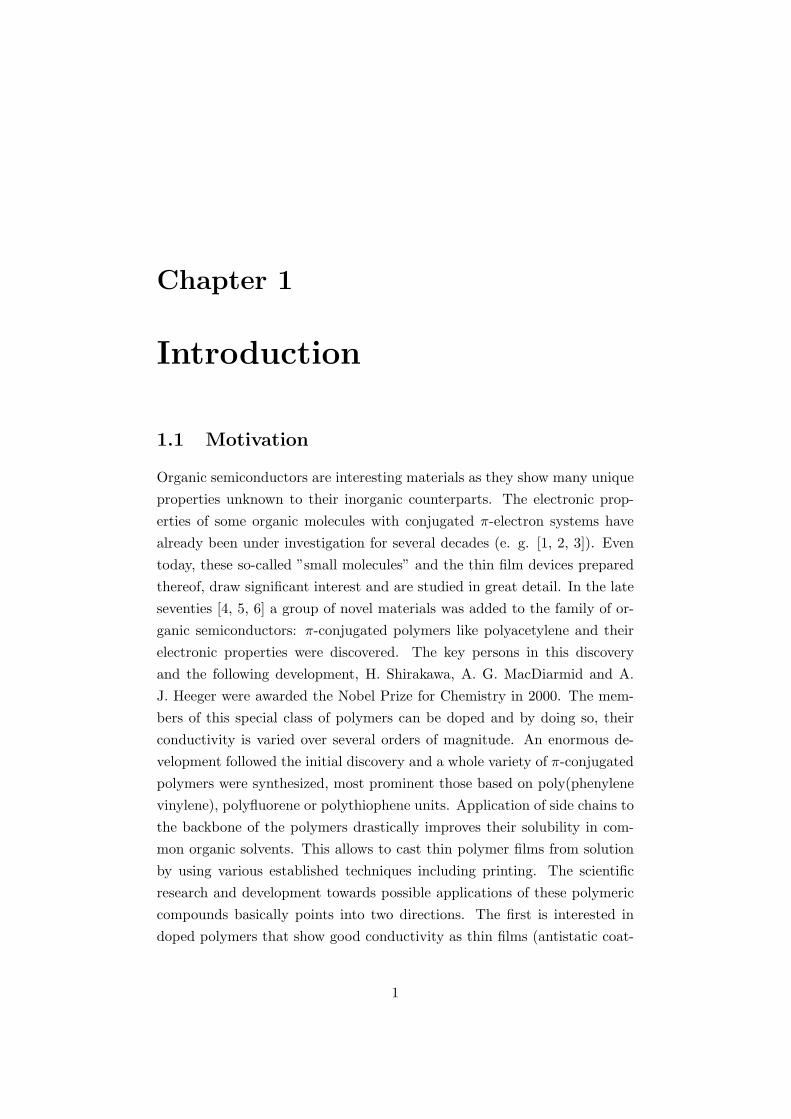
Figure 1.1: Scheme depicting the relevant energy levels for ITO - PE-DOT:PSS - MDMO-PPV thin film devices with various top electrodes. Dueto our experimental results energetic alignment between the highest occu-pied molecular level (HOMO) of MDMO-PPV and PEDOT:PSS as well asbetween the lowest unoccupied molecular level (LUMO) of MDMO-PPVand LiF/Al is assumed. Interface effects are not included in the scheme.
in which an electron donating species (the π-conjugated polymer) is blendedwith an electron accepting species (the fullerene derivative) [22, 23].
1.3.1 Slightly doped π-conjugated polymers
MDMO-PPV is used as a model system, because it is known for its lowamount of mobile charge carriers in the dark. Figure 1.1 displays the relevantenergy levels of the studied devices. Indium tin oxide (ITO) covered with alayer of poly(3,4-ethylenedioxythiophene) doped with poly(styrenesulfonate)(PEDOT:PSS) is employed as hole injecting contact. It is the same in alldevices, whereas the electron injecting contact is changed from Au via Al toLiF/Al. The work functions of Al, Au [24] and PEDOT:PSS are plotted inFig. 1.1 together with the highest occupied (HOMO) and the lowest unoc-
4
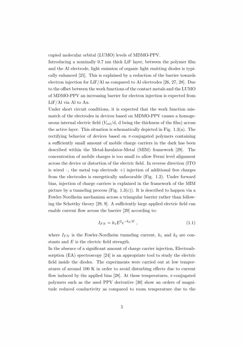
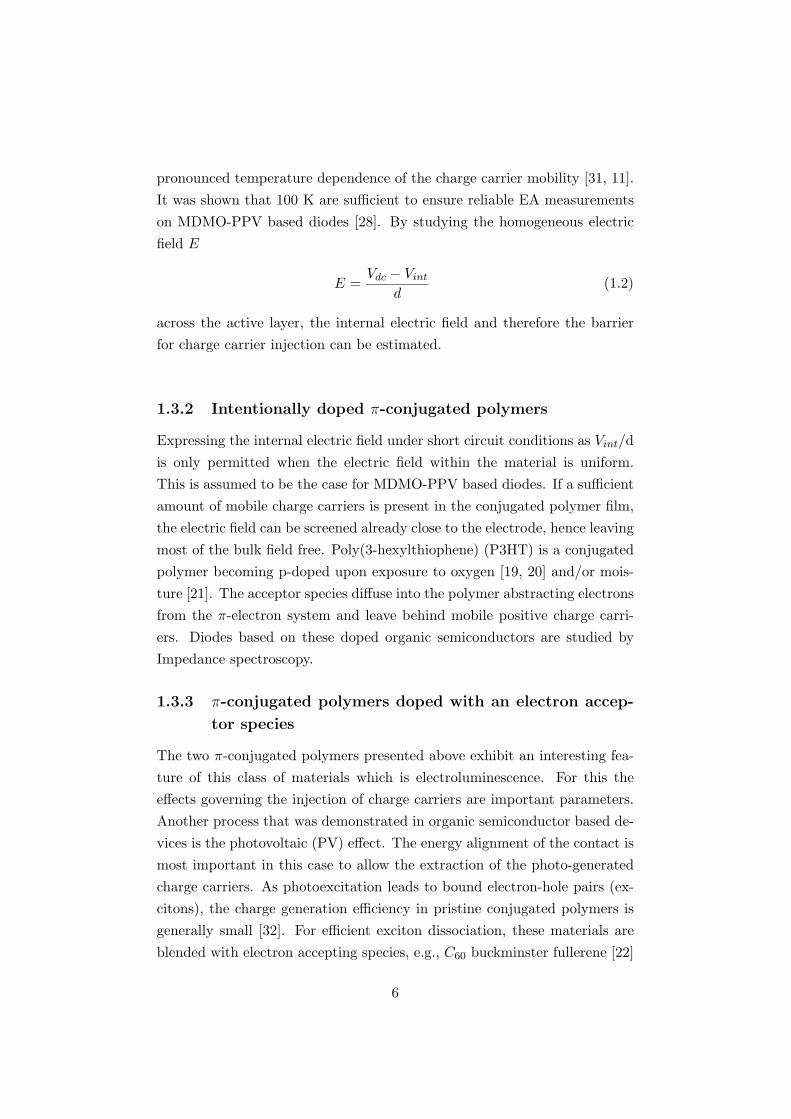
cupied molecular orbital (LUMO) levels of MDMO-PPV.Introducing a nominally 0.7 nm thick LiF layer, between the polymer filmand the Al electrode, light emission of organic light emitting diodes is typi-cally enhanced [25]. This is explained by a reduction of the barrier towardselectron injection for LiF/Al as compared to Al electrodes [26, 27, 28]. Dueto the offset between the work functions of the contact metals and the LUMOof MDMO-PPV an increasing barrier for electron injection is expected fromLiF/Al via Al to Au.Under short circuit conditions, it is expected that the work function mis-match of the electrodes in devices based on MDMO-PPV causes a homoge-neous internal electric field (Vint/d, d being the thickness of the film) acrossthe active layer. This situation is schematically depicted in Fig. 1.3(a). Therectifying behavior of devices based on π-conjugated polymers containinga sufficiently small amount of mobile charge carriers in the dark has beendescribed within the Metal-Insulator-Metal (MIM) framework [29]. Theconcentration of mobile charges is too small to allow Fermi level alignmentacross the device or distortion of the electric field. In reverse direction (ITOis wired –, the metal top electrode +) injection of additional free chargesfrom the electrodes is energetically unfavorable (Fig. 1.2). Under forwardbias, injection of charge carriers is explained in the framework of the MIMpicture by a tunneling process (Fig. 1.3(c)). It is described to happen via aFowler-Nordheim mechanism across a triangular barrier rather than follow-ing the Schottky theory [29, 9]. A sufficiently large applied electric field canenable current flow across the barrier [29] according to:
IFN = k1E2e−k2/E , (1.1)
where IFN is the Fowler-Nordheim tunneling current, k1 and k2 are con-stants and E is the electric field strength.In the absence of a significant amount of charge carrier injection, Electroab-sorption (EA) spectroscopy [24] is an appropriate tool to study the electricfield inside the diodes. The experiments were carried out at low temper-atures of around 100 K in order to avoid disturbing effects due to currentflow induced by the applied bias [28]. At these temperatures, π-conjugatedpolymers such as the used PPV derivative [30] show an orders of magni-tude reduced conductivity as compared to room temperature due to the
5
pronounced temperature dependence of the charge carrier mobility [31, 11].It was shown that 100 K are sufficient to ensure reliable EA measurementson MDMO-PPV based diodes [28]. By studying the homogeneous electricfield E
E =Vdc − Vint
d(1.2)
across the active layer, the internal electric field and therefore the barrierfor charge carrier injection can be estimated.
1.3.2 Intentionally doped π-conjugated polymers
Expressing the internal electric field under short circuit conditions as Vint/dis only permitted when the electric field within the material is uniform.This is assumed to be the case for MDMO-PPV based diodes. If a sufficientamount of mobile charge carriers is present in the conjugated polymer film,the electric field can be screened already close to the electrode, hence leavingmost of the bulk field free. Poly(3-hexylthiophene) (P3HT) is a conjugatedpolymer becoming p-doped upon exposure to oxygen [19, 20] and/or mois-ture [21]. The acceptor species diffuse into the polymer abstracting electronsfrom the π-electron system and leave behind mobile positive charge carri-ers. Diodes based on these doped organic semiconductors are studied byImpedance spectroscopy.
1.3.3 π-conjugated polymers doped with an electron accep-
tor species
The two π-conjugated polymers presented above exhibit an interesting fea-ture of this class of materials which is electroluminescence. For this theeffects governing the injection of charge carriers are important parameters.Another process that was demonstrated in organic semiconductor based de-vices is the photovoltaic (PV) effect. The energy alignment of the contact ismost important in this case to allow the extraction of the photo-generatedcharge carriers. As photoexcitation leads to bound electron-hole pairs (ex-citons), the charge generation efficiency in pristine conjugated polymers isgenerally small [32]. For efficient exciton dissociation, these materials areblended with electron accepting species, e.g., C60 buckminster fullerene [22]
6
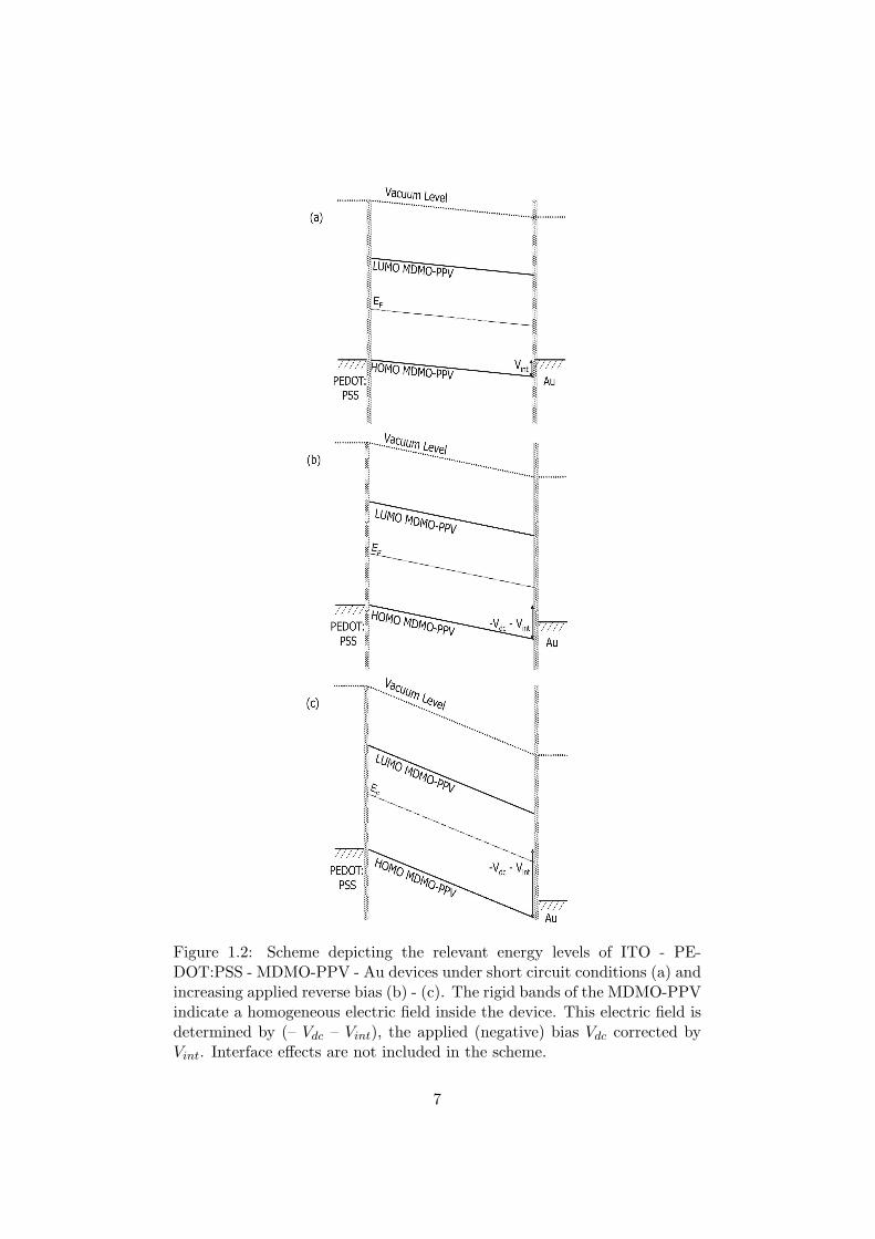
Figure 1.2: Scheme depicting the relevant energy levels of ITO - PE-DOT:PSS - MDMO-PPV - Au devices under short circuit conditions (a) andincreasing applied reverse bias (b) - (c). The rigid bands of the MDMO-PPVindicate a homogeneous electric field inside the device. This electric field isdetermined by (– Vdc – Vint), the applied (negative) bias Vdc corrected byVint. Interface effects are not included in the scheme.
7
Figure 1.3: Scheme depicting the relevant energy levels of ITO - PE-DOT:PSS - MDMO-PPV - Al devices under short circuit conditions (a), flat-band conditions (b) and forward bias (c). The rigid bands of the MDMO-PPV indicate a homogeneous electric field inside the device. A triangularbarrier for electron injection is schematically depicted in (c). Interface effectsare not included in the scheme.
8
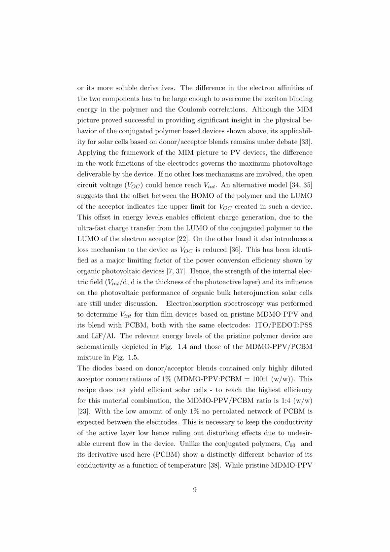
or its more soluble derivatives. The difference in the electron affinities ofthe two components has to be large enough to overcome the exciton bindingenergy in the polymer and the Coulomb correlations. Although the MIMpicture proved successful in providing significant insight in the physical be-havior of the conjugated polymer based devices shown above, its applicabil-ity for solar cells based on donor/acceptor blends remains under debate [33].Applying the framework of the MIM picture to PV devices, the differencein the work functions of the electrodes governs the maximum photovoltagedeliverable by the device. If no other loss mechanisms are involved, the opencircuit voltage (VOC) could hence reach Vint. An alternative model [34, 35]suggests that the offset between the HOMO of the polymer and the LUMOof the acceptor indicates the upper limit for VOC created in such a device.This offset in energy levels enables efficient charge generation, due to theultra-fast charge transfer from the LUMO of the conjugated polymer to theLUMO of the electron acceptor [22]. On the other hand it also introduces aloss mechanism to the device as VOC is reduced [36]. This has been identi-fied as a major limiting factor of the power conversion efficiency shown byorganic photovoltaic devices [7, 37]. Hence, the strength of the internal elec-tric field (Vint/d, d is the thickness of the photoactive layer) and its influenceon the photovoltaic performance of organic bulk heterojunction solar cellsare still under discussion. Electroabsorption spectroscopy was performedto determine Vint for thin film devices based on pristine MDMO-PPV andits blend with PCBM, both with the same electrodes: ITO/PEDOT:PSSand LiF/Al. The relevant energy levels of the pristine polymer device areschematically depicted in Fig. 1.4 and those of the MDMO-PPV/PCBMmixture in Fig. 1.5.The diodes based on donor/acceptor blends contained only highly dilutedacceptor concentrations of 1% (MDMO-PPV:PCBM = 100:1 (w/w)). Thisrecipe does not yield efficient solar cells - to reach the highest efficiencyfor this material combination, the MDMO-PPV/PCBM ratio is 1:4 (w/w)[23]. With the low amount of only 1% no percolated network of PCBM isexpected between the electrodes. This is necessary to keep the conductivityof the active layer low hence ruling out disturbing effects due to undesir-able current flow in the device. Unlike the conjugated polymers, C60 andits derivative used here (PCBM) show a distinctly different behavior of itsconductivity as a function of temperature [38]. While pristine MDMO-PPV
9

Figure 1.4: Scheme depicting the relevant energy levels of ITO - PE-DOT:PSS - MDMO-PPV - LiF/Al devices under flat band (left) and shortcircuit conditions (right). Interface effects are not included in the scheme.Due to our experiments, an almst ohmic contact between MDMO-PPV andLiF/Al is assumed.
10
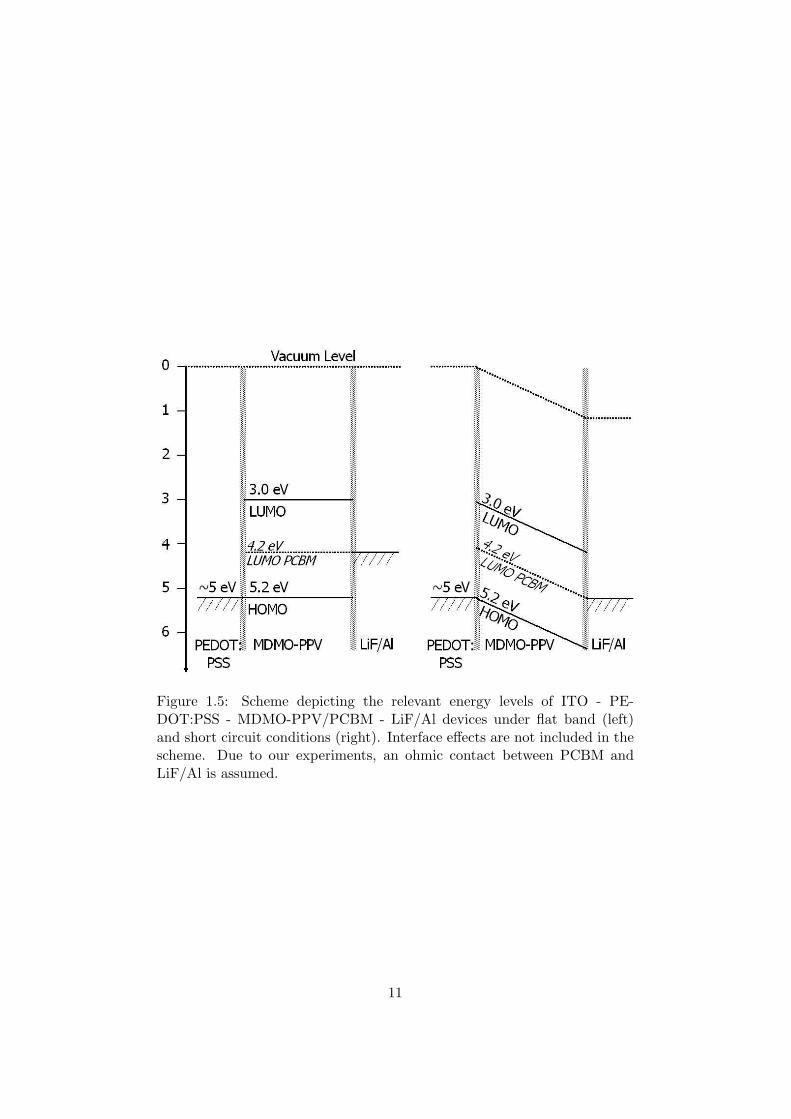
Figure 1.5: Scheme depicting the relevant energy levels of ITO - PE-DOT:PSS - MDMO-PPV/PCBM - LiF/Al devices under flat band (left)and short circuit conditions (right). Interface effects are not included in thescheme. Due to our experiments, an ohmic contact between PCBM andLiF/Al is assumed.
11
acts as electrical insulator at the measuring temperature of EA (≈ 100 K),C60 does not lose its conductive properties.
1.4 Impedance spectroscopy on polymer semicon-
ductor thin film devices
In the MDMO-PPV and P3HT based thin film devices presented above,ohmic contact for holes from the interface with ITO or ITO/PEDOT:PSS isexpected. Upon using these hole injecting electrodes, the electrical proper-ties of the devices are largely influenced by the metal top electrode. Its workfunction is an important parameter for the electron injection into the organicsemiconductor layer. In the studied devices the difference between the semi-conductor bandgap and Vint gives a qualitative estimation for the chancefor bipolar injection, i. e. the injection of both electrons and holes. Thepresence of both types of carriers in the film is the prerequisite for their ra-diative recombination and therefore electroluminescence, one of the desiredand valuable properties of many π-conjugated polymers such as MDMO-PPV and P3HT [39].MDMO-PPV based diodes with Au, Al and LiF/Al top electrodes as well asdoped ITO - P3HT - Al devices are studied with Impedance spectroscopy.This technique is very versatile, as a frequency range over several ordersof magnitude (in this case 20 Hz - 1 MHz) is experimentally accessible. Ittherefore allows to distinguish between phenomena on various time scales.The approach to measure the impedance of conjugated polymer based diodestructures is significantly different from the study of Metal-Insulator-Semiconductor(MIS) devices. Whereas in the MIS structures based on organic semicon-ductors and dielectrics accumulated charges at the semiconductor/insulatorinterface are of primary interest (e.g. [40]), in the diodes it is desired tostudy features related to charge injection, transport and recombination inthe bulk of the organic semiconductor.Generally, the impedance of a device is defined as
vac(ω)iac(ω)
≡ Z(ω) = ReZ + i ImZ , (1.3)
where vac and iac are the applied voltage and the measured current, re-spectively. Z(ω) is the frequency dependent complex impedance, with ReZ
12
and ImZ being its real and imaginary components. The modulus of theimpedance |Z| is hence defined as
|Z| =√
ReZ2 + ImZ2 (1.4)
and its phase θ is derived using
tanθ =ImZ
ReZ. (1.5)
The impedance Z is related to the admittance Y via
1Z(ω)
≡ iac(ω)vac(ω)
≡ Y (ω) = ReY + i ImY , (1.6)
The simplest equivalent circuit to describe a diode is a resistance (Rp) anda capacitance (Cp) in parallel. Hence the admittance can be expressed as:
Y (ω) =1
Rp+ iωCp (1.7)
1.4.1 Space charge limited current
While the MIM picture together with the proposed Fowler-Nordheim tun-neling mechanism [29] gives a reasonable description of the onset of chargeinjection, it fails to correctly describe the current through the device underinjection bias. In PPV based diodes the actual currents turned out to besignificantly smaller than expected due to Fowler-Nordheim tunneling [41].Therefore it was concluded that the tunneling injection mechanism does notlimit the current through the device. Charge transport was identified asthe limiting mechanism and the diode characteristics could be described ac-curately in the well established framework of space charge limited current(SCLC) (e.g. [16]).
1.4.2 Stationary single carrier space charge limited current
Ohmic contacts to space charge limited devices yield nonlinear current - volt-age curves as with increasing voltage both the electric field across the semi-conductor as well as the injected free carrier concentration become larger.The general description of the single carrier dc current density J is given by
13
Ohm’s law
J = en(E)µdcE , (1.8)
where e is the elementary charge (for electrons or holes), n is the number ofmobile charge carriers, µdc is the respective charge carrier drift mobility andE is the electric field strength. As long as the amount of thermally generatedfree charges is small compared to the number of charge carriers injectedfrom the electrodes, it may be neglected and n represents only the injectedcharges. This approximation is justified for most organic semiconductors,where the band-gap is in the order of 2 eV and impurities rather introducetraps than acting as a source of mobile charges [8]. The relation betweenthe total number of charge carriers and the electric field is described by thePoisson equation
n(x) =εε0
q
dE
dx, (1.9)
where ε0 is the permittivity of free space and ε the relative permittivity ofthe semiconductor. Plugging Eq. (1.9) into Eq. (1.8) yields the differentialequation
J = εε0µdcE(x)dE
dx, (1.10)
which is solved under the boundary condition E(x = 0) = 0 by
E(x) =
√2J
εε0µdcx. (1.11)
From integrating the electric field (Eq. (1.11)) from the injecting x = 0 tothe extracting electrode x = d the voltage V (x) is obtained:
V (x) =∫ d
0E(x) dx =
√8J
9εε0µdcx3/2 . (1.12)
Taking x = d and V = V (x = d), the current density - voltage relation
J =98εε0µdc
V 2
d3, (1.13)
14
is obtained in the form of the famous Mott-Gurney square law, also knownas Child’s law for solids [16]. Combining Eq. (1.13) with Eq. (1.11) allowsto describe the electric field strength between the electrodes
E(x) =3V
2d
√x
d. (1.14)
Knowing the electric field inside the semiconductor film allows to determinethe interelectrode transit time of the charge carriers. The speed of themoving charges v(x) depends on their mobility µdc and the electric fieldE(x) inside the semiconductor and is described by
v(x) = µdcE(x) . (1.15)
Hence the transit time τtr can be determined by
τtr =∫ L
0
1v(x)
dx =1
µdc
∫ d
0
1E(x)
dx . (1.16)
The electric field E(x) is described by Eq. (1.14), which can be plugged intoEq. (1.16). After integration the following relation between the transit timeand the charge carrier mobility is established:
τtr =4d2
3µdcV. (1.17)
In the case of asymmetric electrodes an electric field is present across thesemiconductor even when no external bias is applied. This internal electricfield has to be overcome in order to inject charges into the device. Hencethe externally applied bias has to be corrected by this Vint. Equation (1.17)is therefore transformed into:
τtr =4d2
3µdc(V − Vint). (1.18)
1.4.3 Modeling the admittance of trap-free space charge lim-
ited current diodes
In order to describe SCLC in the case of time dependent electric fields (e.g.alternating current), a displacement term should be added to Ohm’s law
15
introduced above Eq. (1.8). The current density is then given by:
J(t) = qn(x, t)µE(x, t) + εε0∂E(x, t)
∂t, (1.19)
where µ is assumed to be field and time independent. However, to allow fora possible change in the mobility, a normalized, dimensionless mobility isintroduced:
µ =µ(ω)µdc
, (1.20)
where µ(ω) is the frequency dependent mobility and µdc is the dc mobilityintroduced above. If there are no traps in the semiconductor µ = 1.For single carrier SCLC devices theoretical descriptions of the capacitanceare available from the Sixties and Seventies. Shao et al. [42] and Kassing [43]introduced a model for the dynamic, hence frequency dependent admittanceY (ω) of perfect single carrier space charge limited devices without traps. Forthe derivation the small signal approximation is used, i.e. a small ac voltageis superimposed on a large dc bias. The applied voltage is hence expressedby
V (x, t) = Vdc(x) + vac(x, t) = Vdc(x) + Vac(x)eiωt, |vac| << |Vdc|. (1.21)
According to references [43] and [42] the results for the complex admittanceY (ω) = iac/vac can be written as:
Y (ω) =Cg
2µτtr (Ω/µ)3
i[1− e−iΩ/µ] + Ω/µ− (1/2)i(Ω/µ)2 =
=Cg
2τtr Ω3
iµ2[1− e−iΩ] + µΩ− (1/2)iΩ2 , (1.22)
with µ = 1 for trap-free SCLC. For µ = 1 we can separate into real andimaginary part:
Y (ω) =Cg
2τtrΩ3 Ω− sinΩ
(Ω− sinΩ)2 + (1− cosΩ− Ω2/2)2+ i
Ω2/2 + cosΩ− 1(Ω− sinΩ)2 + (1− cosΩ− Ω2/2)2
,(1.23)
where Ω = ωτtr is a ”normalized frequency” and Cg = εA/d is the geometriccapacitance. Defining the dynamic conductance G(ω) and capacitance C(ω)
16
by:
Y (ω) = G(ω) + iωC(ω) , (1.24)
we get:
G(ω) = (G0/6)Ω3 Ω− sinΩ(Ω− sinΩ)2 + (1− cosΩ− Ω2/2)2
, (1.25)
with G0 = G(0) = 3Cg/τtr = 9εµAV/4d3.
C(ω) = (Cg/2)Ω2 Ω2/2 + cosΩ− 1(Ω− sinΩ)2 + (1− cosΩ− Ω2/2)2
. (1.26)
At low frequencies, Ω << 1, G(ω) approaches G0 and C(ω) approaches(3/4)Cg. At high frequencies, Ω >> 1, G(ω) = (2/3)G0 and C(ω) = Cg:Therefore, the sample can be represented at low and high frequencies by anequivalent circuit of a resistance (Rp) and a capacitance (Cp) in parallel,with:
Rp = G−10 ; Cp = (3/4)Cg; at ωτtr << 1
Rp = (3/2)G−10 ; Cp = Cg; at ωτtr >> 1 . (1.27)
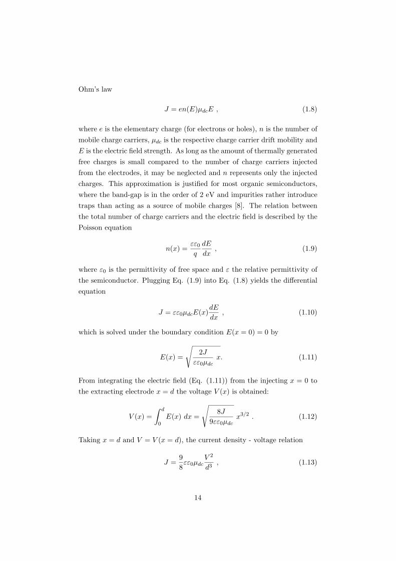
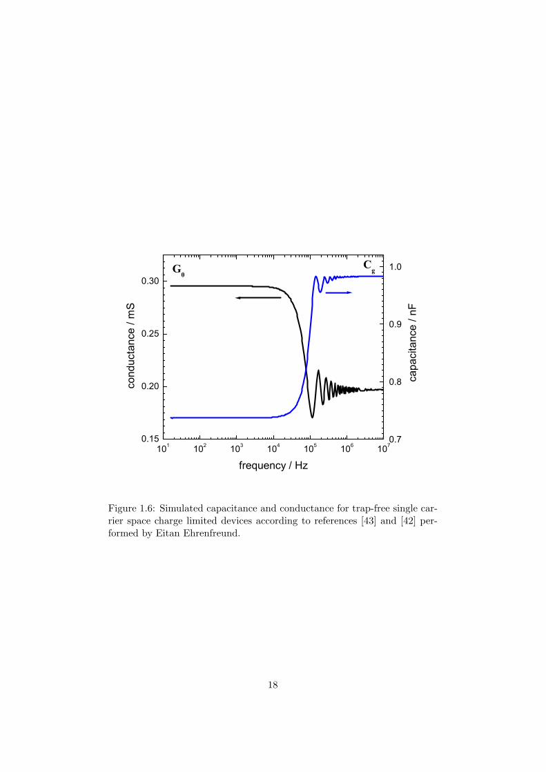
Figure 1.6 shows a simulation of conductance G (Eq. (1.25)) and capac-itance C (Eq. (1.26)) for trap-free single carrier SCLC in a diode. Theimportant parameter governing both contributions to the admittance is thetransit time τtr of the injected charge carriers (Eqs. (1.25) and (1.26)). Intrap-free single carrier SCLC samples the transit time effect caused by thecharge carriers moving from one electrode to the other is identified as theonly influence on the the admittance [44]. The transitions observed in C andG are hence determined to take place at frequencies around (τtr)−1. The lowfrequency values of C and G are affected by these transit time effects as thecharge carriers can be injected and leave the device in the same half periodof the ac voltage. vac can inject additional charge carriers which for frequen-cies f < (τtr)−1 cause additional current. At higher frequencies the othercontact cannot be reached in this time frame, the conductance decreasesand the capacitance increases, finally reaching the geometric capacitance.
17
101 102 103 104 105 106 1070.15
0.20
0.25
0.30
0.7
0.8
0.9
1.0G0
Cg
cond
ucta
nce
/ mS
frequency / Hz
capa
cita
nce
/ nF
Figure 1.6: Simulated capacitance and conductance for trap-free single car-rier space charge limited devices according to references [43] and [42] per-formed by Eitan Ehrenfreund.
18
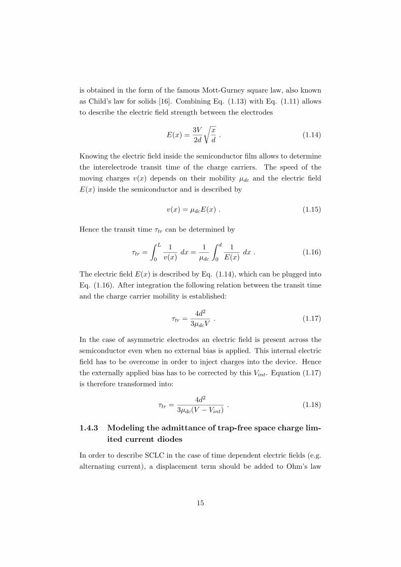
1.4.4 Modeling the admittance of space charge limited cur-
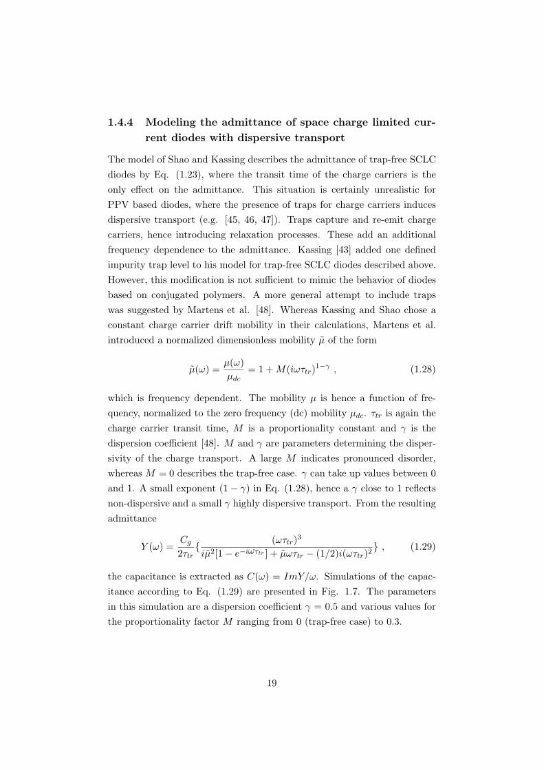
rent diodes with dispersive transport
The model of Shao and Kassing describes the admittance of trap-free SCLCdiodes by Eq. (1.23), where the transit time of the charge carriers is theonly effect on the admittance. This situation is certainly unrealistic forPPV based diodes, where the presence of traps for charge carriers inducesdispersive transport (e.g. [45, 46, 47]). Traps capture and re-emit chargecarriers, hence introducing relaxation processes. These add an additionalfrequency dependence to the admittance. Kassing [43] added one definedimpurity trap level to his model for trap-free SCLC diodes described above.However, this modification is not sufficient to mimic the behavior of diodesbased on conjugated polymers. A more general attempt to include trapswas suggested by Martens et al. [48]. Whereas Kassing and Shao chose aconstant charge carrier drift mobility in their calculations, Martens et al.introduced a normalized dimensionless mobility µ of the form
µ(ω) =µ(ω)µdc
= 1 + M(iωτtr)1−γ , (1.28)
which is frequency dependent. The mobility µ is hence a function of fre-quency, normalized to the zero frequency (dc) mobility µdc. τtr is again thecharge carrier transit time, M is a proportionality constant and γ is thedispersion coefficient [48]. M and γ are parameters determining the disper-sivity of the charge transport. A large M indicates pronounced disorder,whereas M = 0 describes the trap-free case. γ can take up values between 0and 1. A small exponent (1− γ) in Eq. (1.28), hence a γ close to 1 reflectsnon-dispersive and a small γ highly dispersive transport. From the resultingadmittance
Y (ω) =Cg
2τtr (ωτtr)3
iµ2[1− e−iωτtr ] + µωτtr − (1/2)i(ωτtr)2 , (1.29)
the capacitance is extracted as C(ω) = ImY/ω. Simulations of the capac-itance according to Eq. (1.29) are presented in Fig. 1.7. The parametersin this simulation are a dispersion coefficient γ = 0.5 and various values forthe proportionality factor M ranging from 0 (trap-free case) to 0.3.
19
102 103 104 105 1060.5
1.0
1.5
2.0
2.5
M = 0.3 M = 0.1 M = 0.01 M = 0
capa
cita
nce
/ nF
frequency / Hz
Figure 1.7: Simulated capacitance for single carrier space charge limiteddevices taking into account dispersive transport. According to reference[48], simulation performed by Eitan Ehrenfreund.
20
1.4.5 Single carrier drift mobility extracted from impedance
measurements
As the simulation depicted in Fig. 1.7. shows, dispersive transport makes itdifficult to determine the transit time of the charge carriers from admittancedata. Whereas in the trap-free case (Fig. 1.6) a pronounced step indicatesthe transit of the injected charges, traps only allow to observe a depression(Fig. 1.7) when capacitance is plotted as a function of the frequency. As thetransit time depends on the voltages, the position of this depression shifts asthe applied bias is changed. It moves to higher frequencies with increasingforward bias. Such features have already been observed and described inthe literature [49, 50, 51, 48, 44] and have been attributed to space chargelimited current [16, 43, 52, 53, 54, 55]. By fitting experimental admittancedata to Eq. (1.29), the transit time of the injected charges can be determinedfor single carrier space charge limited devices. Using Eq. (1.18) and hencetaking into account Vint allows to determine the mobility of the charges.This procedure can be done directly with Eq. (1.29) using the relation Y =G(ω) + iωC when the used computer software can handle complex numbers(e.g. MATLAB). For other cases (e.g. ORIGIN), the actual separation intoreal and imaginary part is necessary, as the explicit expressions are needed.In the following the explicit expressions for computation of the real andimaginary parts are written. As a first step the dimensionless quantity
Y = (2τt/Ω3Cg)Y (Ω) (1.30)
21
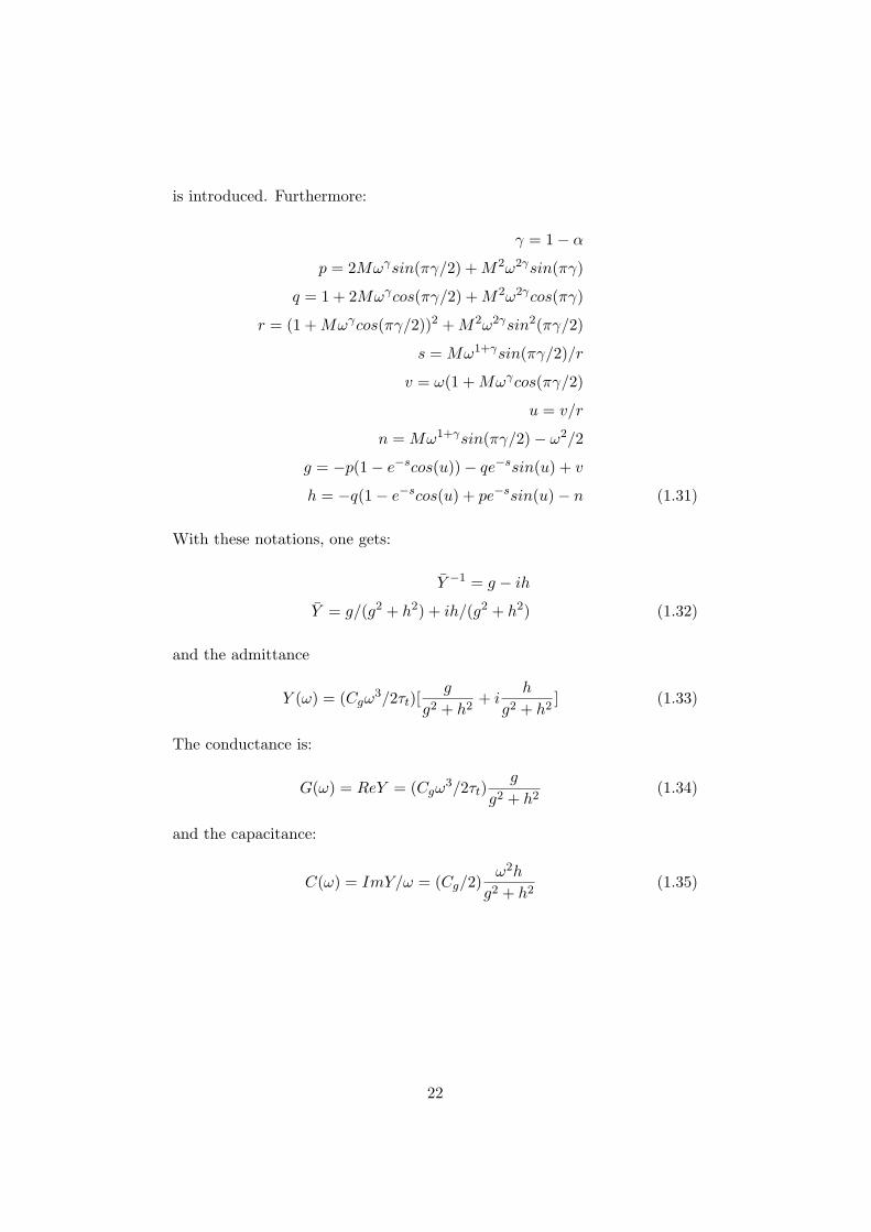
is introduced. Furthermore:
γ = 1− α
p = 2Mωγsin(πγ/2) + M2ω2γsin(πγ)
q = 1 + 2Mωγcos(πγ/2) + M2ω2γcos(πγ)
r = (1 + Mωγcos(πγ/2))2 + M2ω2γsin2(πγ/2)
s = Mω1+γsin(πγ/2)/r
v = ω(1 + Mωγcos(πγ/2)
u = v/r
n = Mω1+γsin(πγ/2)− ω2/2
g = −p(1− e−scos(u))− qe−ssin(u) + v
h = −q(1− e−scos(u) + pe−ssin(u)− n (1.31)
With these notations, one gets:
Y −1 = g − ih
Y = g/(g2 + h2) + ih/(g2 + h2) (1.32)
and the admittance
Y (ω) = (Cgω3/2τt)[
g
g2 + h2+ i
h
g2 + h2] (1.33)
The conductance is:
G(ω) = ReY = (Cgω3/2τt)
g
g2 + h2(1.34)
and the capacitance:
C(ω) = ImY/ω = (Cg/2)ω2h
g2 + h2(1.35)
22
Chapter 2
Experimental
2.1 Device preparation
2.1.1 Substrate preparation
The organic semiconductor thin film devices studied herein were prepared insandwich geometry. Substrates for these devices were 1.5 cm × 1.5 cm largeglass sheets covered with indium tin oxide (ITO, purchased from Merck,Inc.). To ensure secure connection of the metal top electrode without riskingthe connector tip to punch through the metal layer and shortcut to theITO, part of the ITO was removed by chemical wet etching. This wasdone by exposing the surface to a strong acid (HCl conc. : HNO3 conc. :H2O = 4.6 : 0.4 : 5) for 20 minutes. The part where ITO should remainwas coated with scotch tape to protect it from the acid. For thoroughcleaning the substrates subsequently underwent 20 minutes in a basic glasscleaning agent (”Hellmanex”). The remaining Hellmanex was removed withdeionized water in an ultrasonic bath. After drying, the substrates werecovered with PEDOT:PSS or the organic semiconductor layer, dependingon the desired device structure.
2.1.2 Materials
PEDOT:PSS as intermediate layer
Poly(3,4-ethylenedioxythiophene) doped with poly(styrenesulfonate) (in thefollowing abbreviated as PEDOT:PSS, purchased from Bayer AG as BAYTRON-PH) was spin coated onto the ITO. The chemical structure is given in Fig.
23
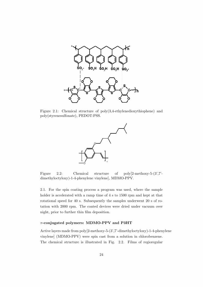
Figure 2.1: Chemical structure of poly(3,4-ethylenedioxythiophene) andpoly(styrenesulfonate), PEDOT:PSS.
Figure 2.2: Chemical structure of poly[2-methoxy-5-(3’,7’-dimethyloctyloxy)-1-4-phenylene vinylene], MDMO-PPV.
2.1. For the spin coating process a program was used, where the sampleholder is accelerated with a ramp time of 4 s to 1500 rpm and kept at thatrotational speed for 40 s. Subsequently the samples underwent 20 s of ro-tation with 2000 rpm. The coated devices were dried under vacuum overnight, prior to further thin film deposition.
π-conjugated polymers: MDMO-PPV and P3HT
Active layers made from poly[2-methoxy-5-(3’,7’-dimethyloctyloxy)-1-4-phenylenevinylene] (MDMO-PPV) were spin cast from a solution in chlorobenzene.The chemical structure is illustrated in Fig. 2.2. Films of regioregular
24
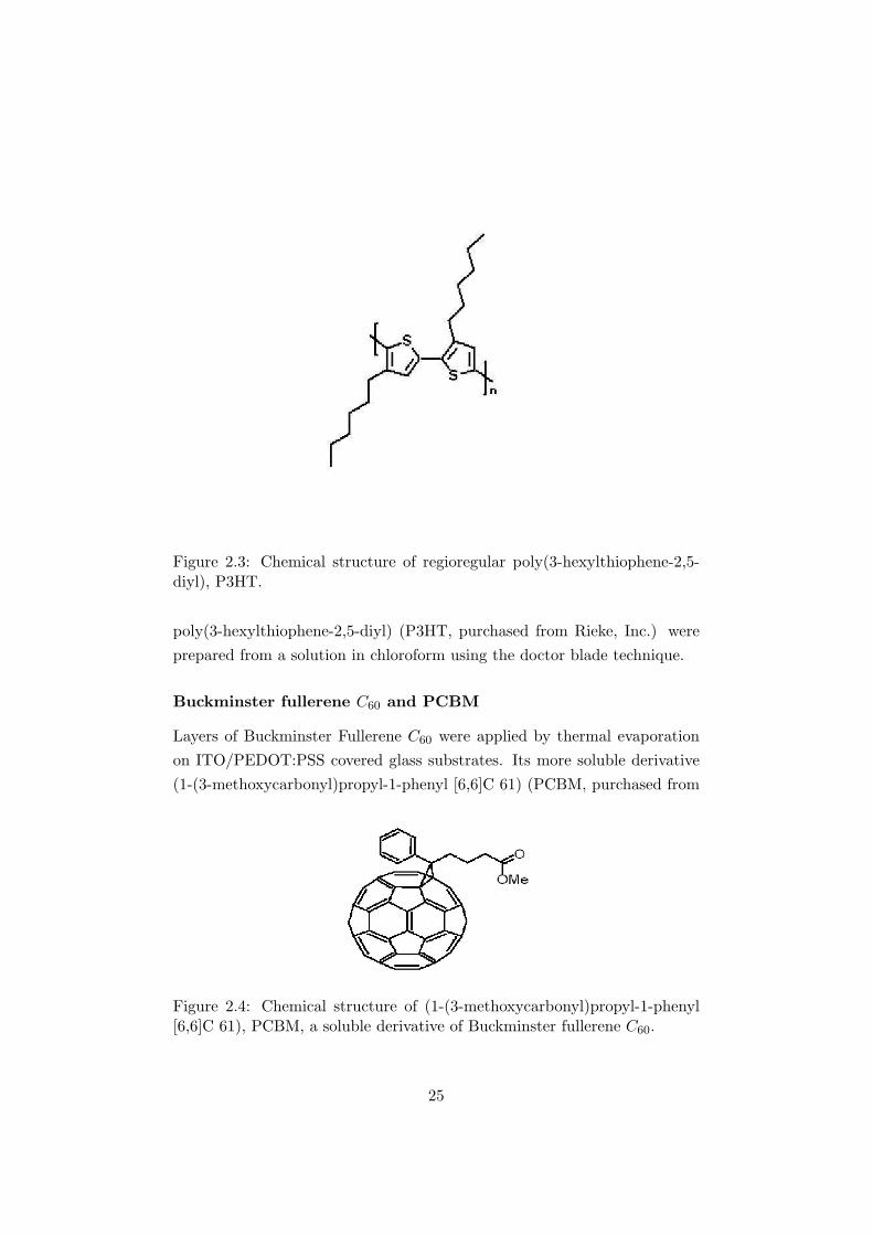
Figure 2.3: Chemical structure of regioregular poly(3-hexylthiophene-2,5-diyl), P3HT.
poly(3-hexylthiophene-2,5-diyl) (P3HT, purchased from Rieke, Inc.) wereprepared from a solution in chloroform using the doctor blade technique.
Buckminster fullerene C60 and PCBM
Layers of Buckminster Fullerene C60 were applied by thermal evaporationon ITO/PEDOT:PSS covered glass substrates. Its more soluble derivative(1-(3-methoxycarbonyl)propyl-1-phenyl [6,6]C 61) (PCBM, purchased from
Figure 2.4: Chemical structure of (1-(3-methoxycarbonyl)propyl-1-phenyl[6,6]C 61), PCBM, a soluble derivative of Buckminster fullerene C60.
25
Nano-C, Inc. The chemical structure is illustrated in Fig. 2.4) was employedas an electron acceptor in blends with MDMO-PPV. The mixtures of bothmaterials were cast from their solution in chlorobenzene.
2.1.3 Evaporation of the top electrodes
The top electrodes were applied by thermal deposition through a shadowmask in vacuum better than 10−5 mbar. Tungsten boats were used as source.Three different contacts were applied for the devices studied herein: Au, Aland LiF/Al. For the first two, layers of around 70 nm were deposited directlyonto the semiconductor films. In the case of LiF/Al electrodes, first LiF wasapplied by evaporating a nominally 0.6 nm thick layer of the salt directlyonto the organic film, afterwards covered by approximately 70 nm Al. Thininterfacial layers of LiF are known to improve electron injection from the Alinto the typical π-conjugated polymers such as PPVs.
2.2 Experimental methods
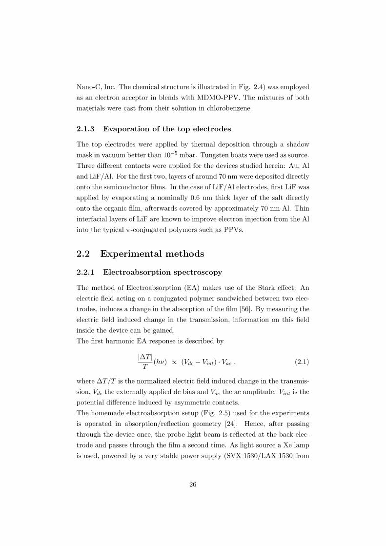
2.2.1 Electroabsorption spectroscopy
The method of Electroabsorption (EA) makes use of the Stark effect: Anelectric field acting on a conjugated polymer sandwiched between two elec-trodes, induces a change in the absorption of the film [56]. By measuring theelectric field induced change in the transmission, information on this fieldinside the device can be gained.The first harmonic EA response is described by
|∆T |T
(hν) ∝ (Vdc − Vint) · Vac , (2.1)
where ∆T/T is the normalized electric field induced change in the transmis-sion, Vdc the externally applied dc bias and Vac the ac amplitude. Vint is thepotential difference induced by asymmetric contacts.The homemade electroabsorption setup (Fig. 2.5) used for the experimentsis operated in absorption/reflection geometry [24]. Hence, after passingthrough the device once, the probe light beam is reflected at the back elec-trode and passes through the film a second time. As light source a Xe lampis used, powered by a very stable power supply (SVX 1530/LAX 1530 from
26
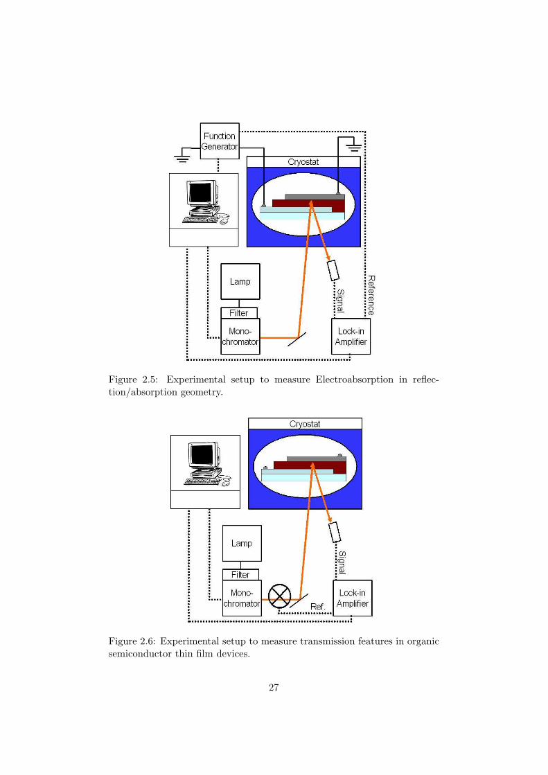
Figure 2.5: Experimental setup to measure Electroabsorption in reflec-tion/absorption geometry.
Figure 2.6: Experimental setup to measure transmission features in organicsemiconductor thin film devices.
27
Muller GmbH Elektronik-Optik). Before entering the monochromator (Ac-ton Research SP-150, 150 g/mm grating, with an 500 nm blaze) the lightbeam passes through a filter, cutting off wavelengths below 450 nm. Theentrance and exit slits are opened by 0.3 mm, a good compromise deliveringsufficient light intensity with a spectral resolution better than 5 nm. Via asystem of three lenses and a mirror for precision alignment, the probe beamis focused onto the active area of the sample inside the cryostat (OxfordInstruments Optistat DN-V), where it is mounted on a cold finger. Thecryostat can be filled with liquid nitrogen. It is therefore possible to coolthe devices to about 77 K. The reflection coming from the Al back electrodeis collected by a lens and focused on a Si-photo diode, delivering a signalproportional to the incoming light intensity to the lock-in amplifier (Stan-ford Research Systems SRS 830).A combined dc and dc voltage produced by the function generator (StanfordResearch Systems DS345) is applied across the sample, connecting the + tothe ITO and the – to the Al. A reference signal of the same frequency andphase is delivered to the lock-in amplifier.If no voltage is applied and instead a chopper wheel is set up in front of themonochromator exit slit, the signal coming from the detector is proportionalto the double path transmission at that wavelength (Fig. 2.6). It can beread out from the lock-in if referenced to the chopping frequency. For everymeasured wavelength the EA response is normalized to this signal to get ridof the spectral response due to the characteristics of the setup.These characteristics include the intensity distribution of the lamp, the per-formance of the monochromator and the sensitivity of the detector.
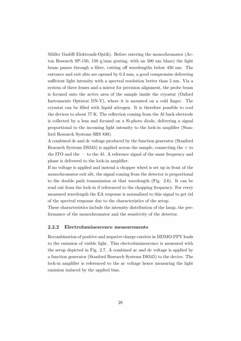
2.2.2 Electroluminescence measurements
Recombination of positive and negative charge carriers in MDMO-PPV leadsto the emission of visible light. This electroluminescence is measured withthe setup depicted in Fig. 2.7. A combined ac and dc voltage is applied bya function generator (Stanford Research Systems DS345) to the device. Thelock-in amplifier is referenced to the ac voltage hence measuring the lightemission induced by the applied bias.
28
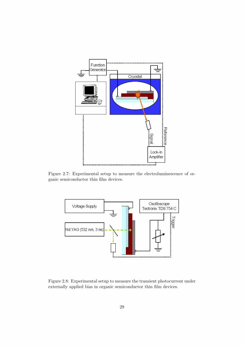
Figure 2.7: Experimental setup to measure the electroluminescence of or-ganic semiconductor thin film devices.
Figure 2.8: Experimental setup to measure the transient photocurrent underexternally applied bias in organic semiconductor thin film devices.
29
2.2.3 Transient photocurrent measurements
The photovoltaic performance of the devices is studied with transient pho-tocurrent measurements under applied bias (Fig. 2.8). Pulsed laser excita-tion (3 ns) using the 532 nm line of a neodymium doped yttrium aluminumgarnet laser (Nd:YAG) was employed. Due to its high amount of photonsdelivered over a short period of time, deterioration of the sample is avoided.By using filters of various optical densities we observed that 0.3 mJ pulsessaturate VOC sufficiently long for the measurements. The laser pulse inducedtransient photocurrents were recorded on devices biased by an external volt-age offset. The photogenerated charge carriers are extracted by the overalldc bias present in the semiconducting layer. Therefore, when this electricfield is compensated externally, i.e., flat-band conditions are established,the created charge carriers cannot leave the device and recombine inside thephotoactive layer. This compensation voltage is referred to as VBI in thefollowing [7]. The transients were recorded by a Tektronix TDS754C oscillo-scope, the offset voltage applied by an Agilent 33250 A function generator.
30
Chapter 3
Results and discussion
3.1 The internal electric field in organic semicon-
ductor thin film devices
In this section, the internal electric field of ITO - PEDOT:PSS - MDMO-PPV devices with various metal top electrodes is studied.
3.1.1 Slightly doped π-conjugated polymers
Figures 3.1 and 3.2 show the normalized electric field induced change intransmission (first harmonic Electroabsorption (EA) response) measured ona typical ITO - PEDOT:PSS - MDMO-PPV - Au device. The EA spectradisplayed in Fig. 3.1 scale with the applied bias as expected from Eq. (2.1):
|∆T |T
(hν) ∝ (Vdc − Vint) · Vac .
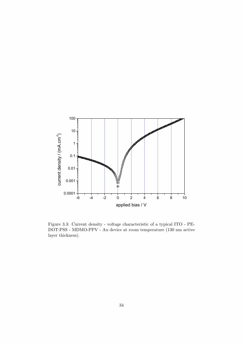
Figure 3.2 shows the EA response at the peak maximum (590 nm). Overthe whole observed voltage range between -4 V and +4 V the electric fieldinduced signal exhibits its predicted linearity with the dc voltage. The EAsignal can be canceled by an externally applied dc voltage (Vdc). Accordingto Eq. (2.1), this is the case for Vdc = Vint, hence determining Vint as +0.7 Vfrom Fig. 3.2. This value does not fit the nominal work function mismatch il-lustrated in Fig. 1.1, from which hardly any potential offset is expected. Onthe other hand a Vint of +0.7 V supports the observed asymmetric currentdensity - voltage (J-V) characteristics shown in Fig. 3.3. The rectificationratio at +/– 6 V is appreciable, exceeding two orders of magnitude. The
31
550
600
650
700
-1.0
-0.5
0.0
0.5
1.0
-4 -3 -2 -1 0 1 2 3 4
-T/
T / 1
0-4
applied bias / V
wavelength / nm
Figure 3.1: First harmonic Electroabsorption spectra of a typical ITO - PE-DOT:PSS - MDMO-PPV - Au device taken at various applied dc voltages.Measurements performed at ≈ 100 K, 1 V ac amplitude.
32
-4 -3 -2 -1 0 1 2 3 40.0
0.2
0.4
0.6
0.8
1.0
|T/
T| /
10-4
applied bias / V
Figure 3.2: First harmonic Electroabsorption data of a typical ITO - PE-DOT:PSS - MDMO-PPV - Au device at various applied bias voltages takenat 590 nm. Measurements performed at ≈ 100 K, 1 V ac amplitude.
33
-6 -4 -2 0 2 4 6 8 100.0001
0.001
0.01
0.1
1
10
100
curr
ent d
ensi
ty /
(mA
.cm
-2)
applied bias / V
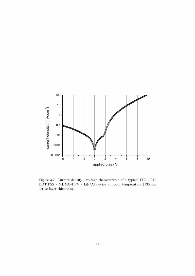
Figure 3.3: Current density - voltage characteristic of a typical ITO - PE-DOT:PSS - MDMO-PPV - Au device at room temperature (130 nm activelayer thickness).
34
-2 -1 0 1 2 30.0
0.1
0.2
0.3
0.4
0.5T/
T / 1
0-4
applied bias / V
Figure 3.4: First harmonic Electroabsorption data of a typical ITO - PE-DOT:PSS - MDMO-PPV - Al device at various applied bias voltages takenat 590 nm. Measurements performed at ≈ 100 K, 1 V ac amplitude.
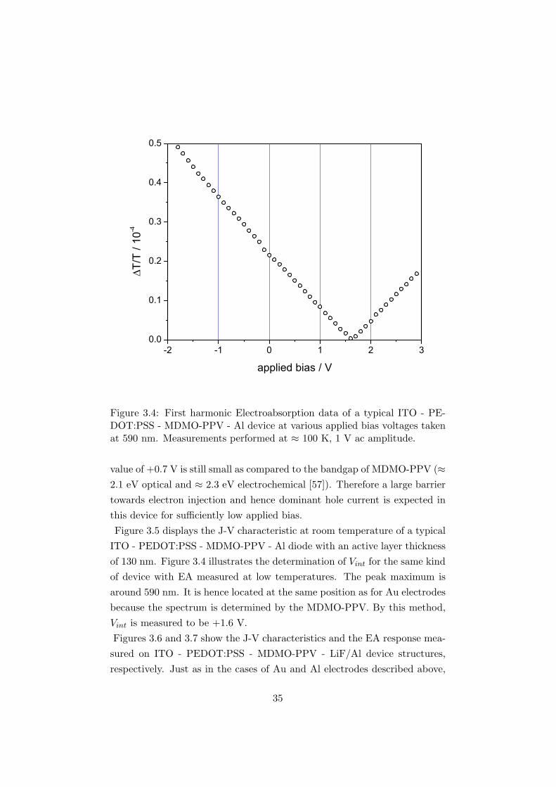
value of +0.7 V is still small as compared to the bandgap of MDMO-PPV (≈2.1 eV optical and ≈ 2.3 eV electrochemical [57]). Therefore a large barriertowards electron injection and hence dominant hole current is expected inthis device for sufficiently low applied bias.Figure 3.5 displays the J-V characteristic at room temperature of a typical
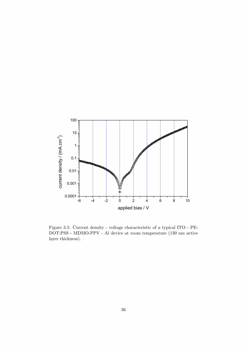
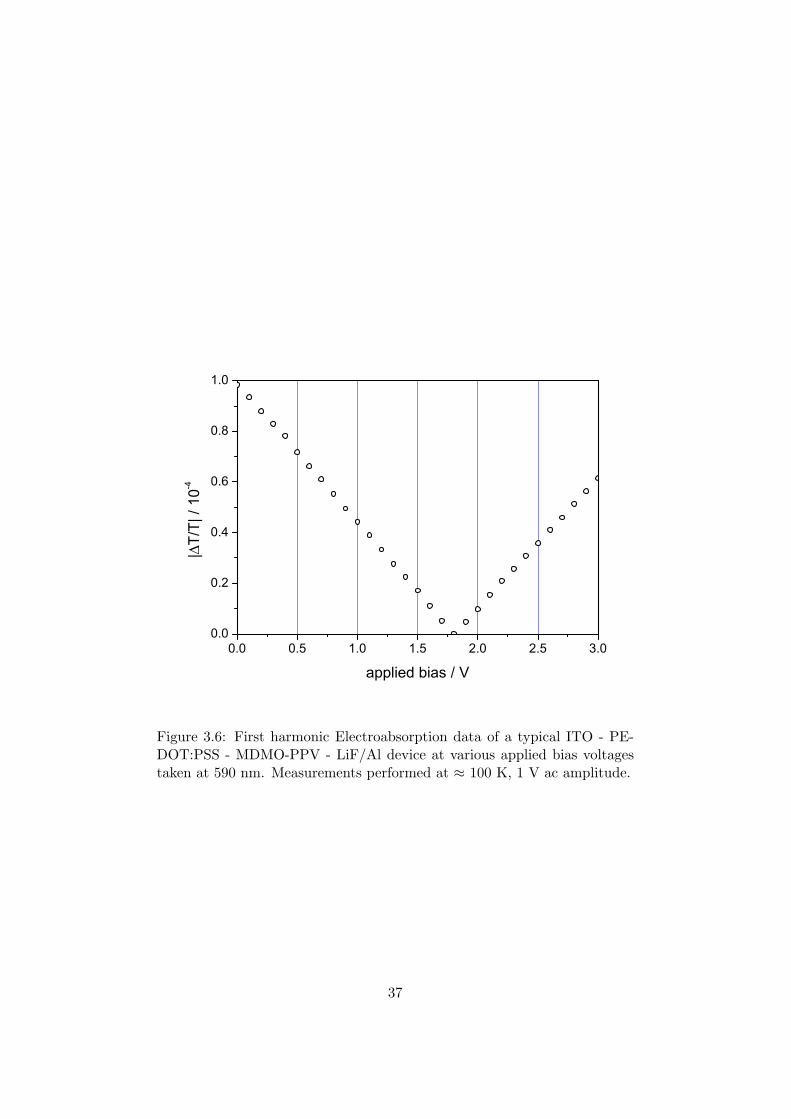
ITO - PEDOT:PSS - MDMO-PPV - Al diode with an active layer thicknessof 130 nm. Figure 3.4 illustrates the determination of Vint for the same kindof device with EA measured at low temperatures. The peak maximum isaround 590 nm. It is hence located at the same position as for Au electrodesbecause the spectrum is determined by the MDMO-PPV. By this method,Vint is measured to be +1.6 V.Figures 3.6 and 3.7 show the J-V characteristics and the EA response mea-sured on ITO - PEDOT:PSS - MDMO-PPV - LiF/Al device structures,respectively. Just as in the cases of Au and Al electrodes described above,
35
-6 -4 -2 0 2 4 6 8 100.0001
0.001
0.01
0.1
1
10
100
curr
ent d
ensi
ty /
(mA
.cm
-2)
applied bias / V
Figure 3.5: Current density - voltage characteristic of a typical ITO - PE-DOT:PSS - MDMO-PPV - Al device at room temperature (130 nm activelayer thickness).
36
0.0 0.5 1.0 1.5 2.0 2.5 3.00.0
0.2
0.4
0.6
0.8
1.0
|T/
T| /
10-4
applied bias / V
Figure 3.6: First harmonic Electroabsorption data of a typical ITO - PE-DOT:PSS - MDMO-PPV - LiF/Al device at various applied bias voltagestaken at 590 nm. Measurements performed at ≈ 100 K, 1 V ac amplitude.
37
-6 -4 -2 0 2 4 6 8 100.0001
0.001
0.01
0.1
1
10
100
curr
ent d
ensi
ty /
(mA
.cm
-2)
applied bias / V
Figure 3.7: Current density - voltage characteristic of a typical ITO - PE-DOT:PSS - MDMO-PPV - LiF/Al device at room temperature (130 nmactive layer thickness).
38
1.0 1.5 2.0 2.5 3.0 3.5 4.010-6
10-5
10-4
10-3
10-2
10-1
applied bias / V
emitt
ed li
ght /
a. u
.
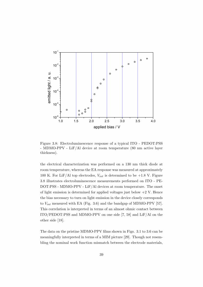
Figure 3.8: Electroluminescence response of a typical ITO - PEDOT:PSS- MDMO-PPV - LiF/Al device at room temperature (80 nm active layerthickness).
the electrical characterization was performed on a 130 nm thick diode atroom temperature, whereas the EA response was measured at approximately100 K. For LiF/Al top electrodes, Vint is determined to be +1.8 V. Figure3.8 illustrates electroluminescence measurements performed on ITO - PE-DOT:PSS - MDMO-PPV - LiF/Al devices at room temperature. The onsetof light emission is determined for applied voltages just below +2 V. Hencethe bias necessary to turn on light emission in the device closely correspondsto Vint measured with EA (Fig. 3.6) and the bandgap of MDMO-PPV [57].This correlation is interpreted in terms of an almost ohmic contact betweenITO/PEDOT:PSS and MDMO-PPV on one side [7, 58] and LiF/Al on theother side [18].
The data on the pristine MDMO-PPV films shown in Figs. 3.1 to 3.6 can bemeaningfully interpreted in terms of a MIM picture [29]. Though not resem-bling the nominal work function mismatch between the electrode materials,
39
Vint can be shifted from +0.7 V (Au) up to +1.8 V by using LiF/Al topelectrodes. The energetic offset between the work functions of the metalsand the energy levels of the organic material is only a first approximationfor the energy barrier towards charge injection. Explanations for the devia-tion between the work function difference of the electrode materials and theactual Vint determined by EA spectroscopy are suggested in various publi-cations: The work functions of the pure metals are usually determined inultra-high vacuum by photoelectron spectroscopy, while the energy levelsin organic molecules are measured by cyclic voltammetry in solution. Thepreparation method of the organic semiconductor thin film devices presentedherein was not clean enough to exclude the oxidation of the metal electrodesor the formation of adsorbate layers. Also chemical reactions are possiblytaking place between the polymer film and the metals that would form aninterfacial layer with properties deviating from those of the bulk [59, 60, 8].Nevertheless, it has to be pointed out that upon changing the top electrodematerial from Au to Al, Vint changes from +0.7 V to +1.6 V. The workfunctions attributed to these metals are 4.3 eV and 5.1 eV respectively [24].Hence the change in Vint is 0.9 V and therefore very close to the differencein the work functions (0.8 V).
3.1.2 Intentionally doped π-conjugated polymers
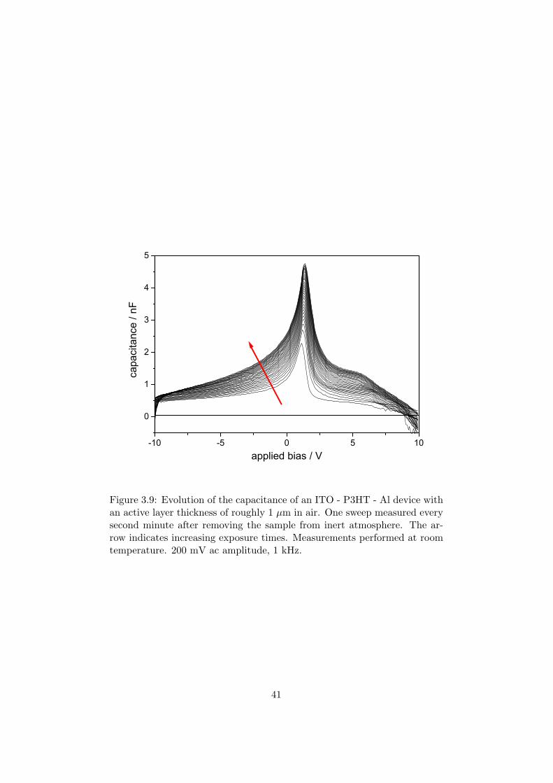
Expressing the internal electric field under short circuit conditions as Vint/dis only permitted when the electric field within the material is homoge-neous. This is assumed to be the case for MDMO-PPV based diodes. If asufficient amount of mobile charge carriers is present in the conjugated poly-mer film, the electric field can be screened already close to the electrode,hence leaving most of the bulk field free. Poly(3-hexylthiophene) (P3HT) isa conjugated polymer becoming p-doped upon exposure to oxygen [19, 20]and/or moisture [21]. Thin film devices based on organic semiconductorsresemble parallel plate capacitors with the low mobility conjugated poly-mers as dielectric. The capacitance C displayed in Fig. 3.9 is extractedfrom the admittance Y measured on the device according to C = ImY/ω.Figure 3.9 shows the evolution of the capacitance C of a P3HT based de-vice as a function of voltage during the exposure to atmosphere. As canbe seen in Fig. 3.9, the capacitance increases with time as long as it is ex-
40
-10 -5 0 5 10
0
1
2
3
4
5
capa
cita
nce
/ nF
applied bias / V
Figure 3.9: Evolution of the capacitance of an ITO - P3HT - Al device withan active layer thickness of roughly 1 µm in air. One sweep measured everysecond minute after removing the sample from inert atmosphere. The ar-row indicates increasing exposure times. Measurements performed at roomtemperature. 200 mV ac amplitude, 1 kHz.
41
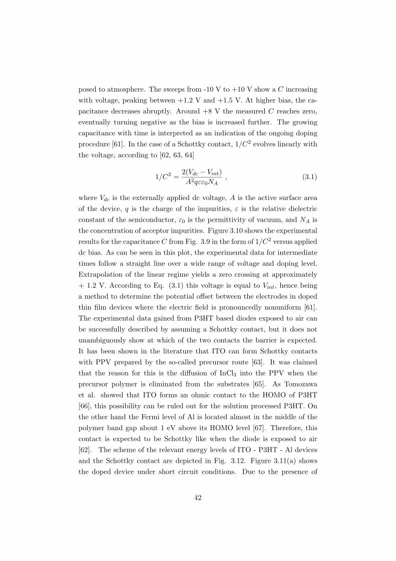
posed to atmosphere. The sweeps from -10 V to +10 V show a C increasingwith voltage, peaking between +1.2 V and +1.5 V. At higher bias, the ca-pacitance decreases abruptly. Around +8 V the measured C reaches zero,eventually turning negative as the bias is increased further. The growingcapacitance with time is interpreted as an indication of the ongoing dopingprocedure [61]. In the case of a Schottky contact, 1/C2 evolves linearly withthe voltage, according to [62, 63, 64]
1/C2 =2(Vdc − Vint)A2qεε0NA
, (3.1)
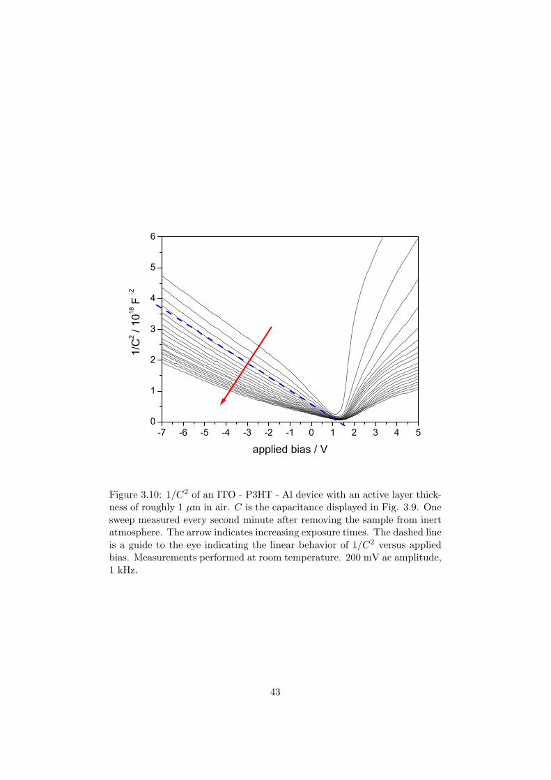
where Vdc is the externally applied dc voltage, A is the active surface areaof the device, q is the charge of the impurities, ε is the relative dielectricconstant of the semiconductor, ε0 is the permittivity of vacuum, and NA isthe concentration of acceptor impurities. Figure 3.10 shows the experimentalresults for the capacitance C from Fig. 3.9 in the form of 1/C2 versus applieddc bias. As can be seen in this plot, the experimental data for intermediatetimes follow a straight line over a wide range of voltage and doping level.Extrapolation of the linear regime yields a zero crossing at approximately+ 1.2 V. According to Eq. (3.1) this voltage is equal to Vint, hence beinga method to determine the potential offset between the electrodes in dopedthin film devices where the electric field is pronouncedly nonuniform [61].The experimental data gained from P3HT based diodes exposed to air canbe successfully described by assuming a Schottky contact, but it does notunambiguously show at which of the two contacts the barrier is expected.It has been shown in the literature that ITO can form Schottky contactswith PPV prepared by the so-called precursor route [63]. It was claimedthat the reason for this is the diffusion of InCl3 into the PPV when theprecursor polymer is eliminated from the substrates [65]. As Tomozawaet al. showed that ITO forms an ohmic contact to the HOMO of P3HT[66], this possibility can be ruled out for the solution processed P3HT. Onthe other hand the Fermi level of Al is located almost in the middle of thepolymer band gap about 1 eV above its HOMO level [67]. Therefore, thiscontact is expected to be Schottky like when the diode is exposed to air[62]. The scheme of the relevant energy levels of ITO - P3HT - Al devicesand the Schottky contact are depicted in Fig. 3.12. Figure 3.11(a) showsthe doped device under short circuit conditions. Due to the presence of
42
-7 -6 -5 -4 -3 -2 -1 0 1 2 3 4 50
1
2
3
4
5
6
applied bias / V
1/C
2 / 10
18 F
-2
Figure 3.10: 1/C2 of an ITO - P3HT - Al device with an active layer thick-ness of roughly 1 µm in air. C is the capacitance displayed in Fig. 3.9. Onesweep measured every second minute after removing the sample from inertatmosphere. The arrow indicates increasing exposure times. The dashed lineis a guide to the eye indicating the linear behavior of 1/C2 versus appliedbias. Measurements performed at room temperature. 200 mV ac amplitude,1 kHz.
43
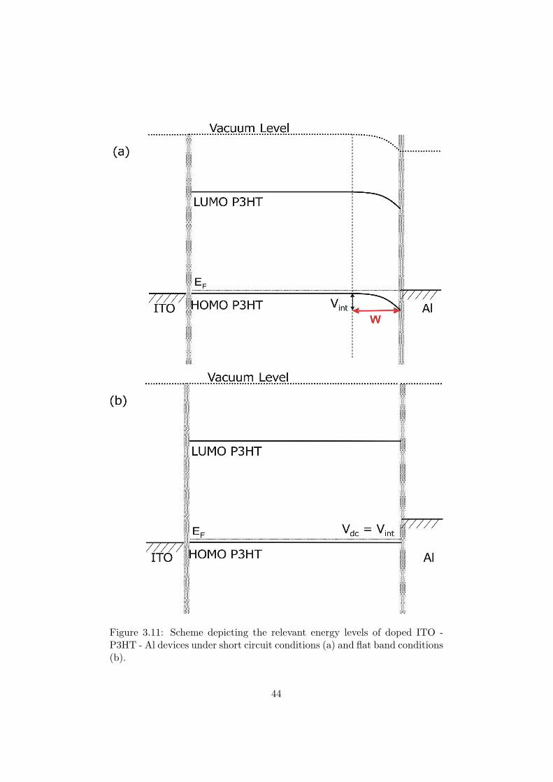
Figure 3.11: Scheme depicting the relevant energy levels of doped ITO -P3HT - Al devices under short circuit conditions (a) and flat band conditions(b).
44
Figure 3.12: Scheme depicting the relevant energy levels of doped ITO -P3HT - Al devices under increasing applied reverse bias from (a) to (b).The electric field is already screened within the depletion zone width Wleaving most of the polymer field free. (–Vdc – Vint) indicates the applied(negative) bias Vdc is corrected by Vint.
45
a significant amount of charge carriers (NA ≈ 1017 in this case [61]), theFermi level aligns between the doped P3HT and the Al contact. The mobilepositive charges induced by the doping procedure recombine with electronsinjected from the Al electrode. The remaining immobile negative chargesscreen Vint already in the vicinity of the Al contact. Figure 3.12(b) and (c)illustrate the device under reverse bias. The increasingly negative voltagecause a growing depletion zone width over which the potential drop takesplace, while the rest of the P3HT film remains field free.Contrary to their counterparts based on MDMO-PPV, which are shown tofollow the MIM scheme, doped P3HT based devices behave differently dueto this doping effect and are well described by assuming a Schottky contact.
3.1.3 π-conjugated polymers doped with an electron accep-
tor species
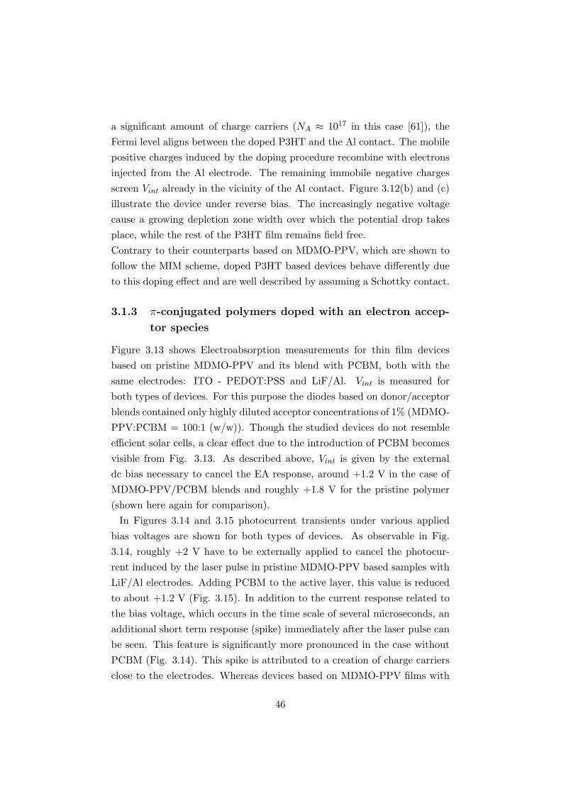
Figure 3.13 shows Electroabsorption measurements for thin film devicesbased on pristine MDMO-PPV and its blend with PCBM, both with thesame electrodes: ITO - PEDOT:PSS and LiF/Al. Vint is measured forboth types of devices. For this purpose the diodes based on donor/acceptorblends contained only highly diluted acceptor concentrations of 1% (MDMO-PPV:PCBM = 100:1 (w/w)). Though the studied devices do not resembleefficient solar cells, a clear effect due to the introduction of PCBM becomesvisible from Fig. 3.13. As described above, Vint is given by the externaldc bias necessary to cancel the EA response, around +1.2 V in the case ofMDMO-PPV/PCBM blends and roughly +1.8 V for the pristine polymer(shown here again for comparison).
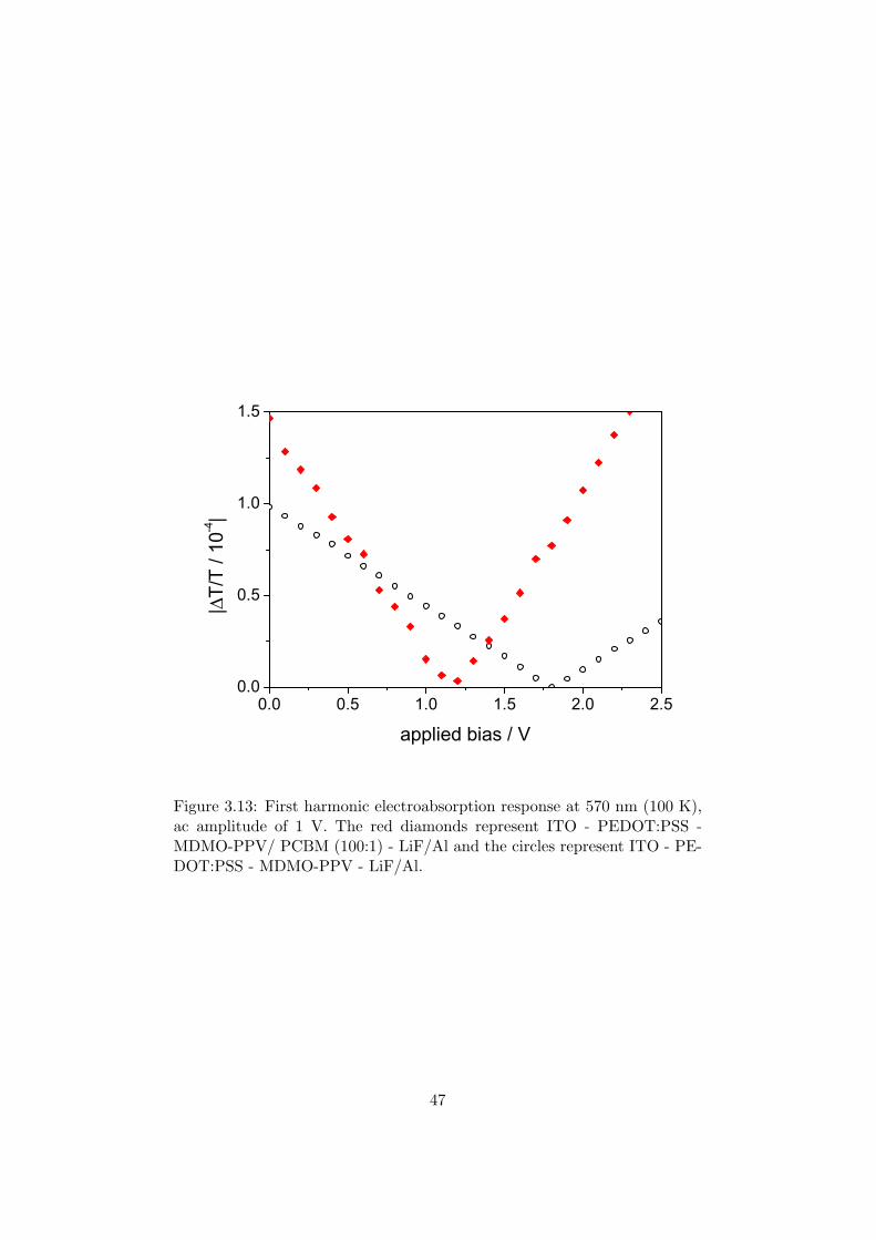
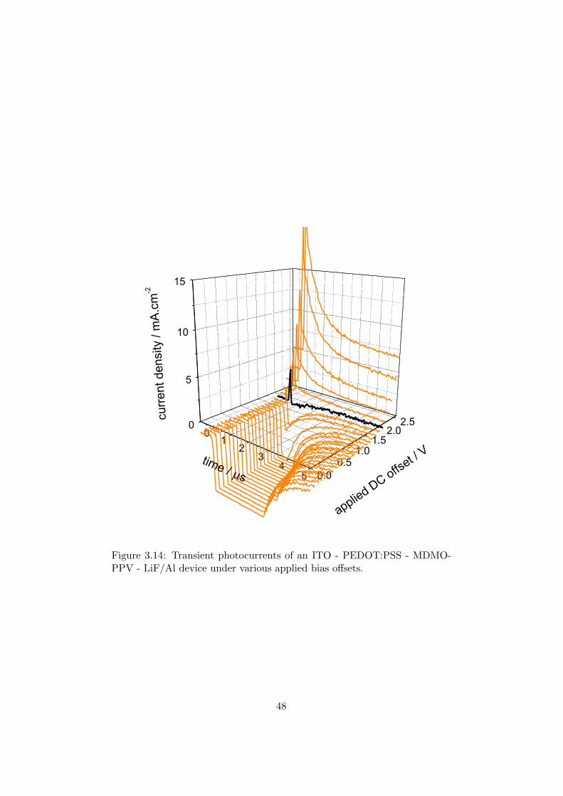
In Figures 3.14 and 3.15 photocurrent transients under various appliedbias voltages are shown for both types of devices. As observable in Fig.3.14, roughly +2 V have to be externally applied to cancel the photocur-rent induced by the laser pulse in pristine MDMO-PPV based samples withLiF/Al electrodes. Adding PCBM to the active layer, this value is reducedto about +1.2 V (Fig. 3.15). In addition to the current response related tothe bias voltage, which occurs in the time scale of several microseconds, anadditional short term response (spike) immediately after the laser pulse canbe seen. This feature is significantly more pronounced in the case withoutPCBM (Fig. 3.14). This spike is attributed to a creation of charge carriersclose to the electrodes. Whereas devices based on MDMO-PPV films with
46
0.0 0.5 1.0 1.5 2.0 2.50.0
0.5
1.0
1.5
|T/
T / 1
0-4|
applied bias / V
Figure 3.13: First harmonic electroabsorption response at 570 nm (100 K),ac amplitude of 1 V. The red diamonds represent ITO - PEDOT:PSS -MDMO-PPV/ PCBM (100:1) - LiF/Al and the circles represent ITO - PE-DOT:PSS - MDMO-PPV - LiF/Al.
47
01
23
45
0
5
10
15
0.00.5
1.01.5
2.02.5cu
rrent
den
sity
/ m
A.cm
-2
applied DC offset / Vtime / s
Figure 3.14: Transient photocurrents of an ITO - PEDOT:PSS - MDMO-PPV - LiF/Al device under various applied bias offsets.
48
01
23
45
0
5
10
15
0.0
0.5
1.01.5cu
rrent
den
sity
/ m
A.cm
-2
applied DC offset / Vtime / s
Figure 3.15: Transient photocurrents of an ITO - PEDOT:PSS - MDMO-PPV/PCBM (100:1) - LiF/Al device under various applied bias offsets.
49
PCBM have efficient exciton dissociation sites in the bulk, in the pristinepolymer charge carriers are generated close to the electrode [68].The photogenerated charge carriers are extracted by the overall dc biaspresent in the semiconducting layer. Therefore, when this electric field iscompensated externally, i.e. flat-band conditions are established, the createdcharge carriers cannot leave the device and recombine inside the photoactivelayer. For the diodes based on pure MDMO-PPV, LiF/Al top electrodes en-sure good electron contact to the LUMO of the conjugated polymer. EAmeasurements on conjugated polymers doped with C60 have shown that dueto electron transfer to the C60 the Fermi level of the low work functionelectrode is pinned close to the LUMO of the acceptor [69]. In the studieddevices, which contain about 1% of PCBM, Vint is determined to be +1.2 V.Again, pinning of the Fermi level to the LUMO of PCBM is the reason forthis value. By space charge limited current measurements, a Vint of +1 Vwas found for ITO - PEDOT:PSS - PCBM - LiF/Al devices [38]. The differ-ence of 0.2 V between these pristine PCBM based devices and our results isattributed to the different matrix conditions. Energy values are sensitive tothe environment and may be altered when PCBM is embedded into MDMO-PPV. According to previous work done by our group, the LUMO of PCBMis estimated to be approximately 4.3 eV [70]. Correlating Vint found by EAspectroscopy with transient photocurrent measurements under applied bias,the overall dc field inside the photoactive layer is identified as the drivingforce of the photocurrent in the solar cell [18]. The same trend is observedfor the transient photocurrent measurements under applied bias.
3.2 Impedance spectroscopy on polymer semicon-
ductor thin film devices
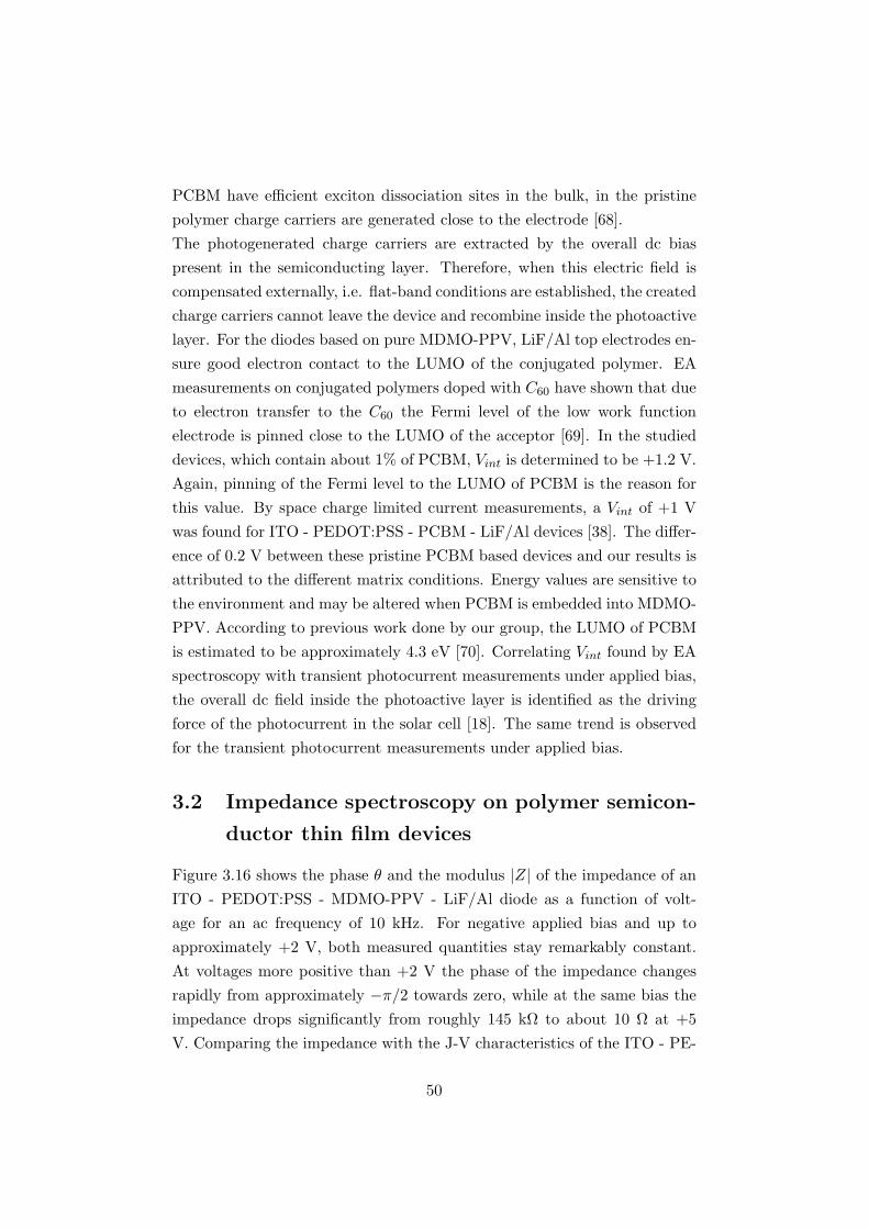
Figure 3.16 shows the phase θ and the modulus |Z| of the impedance of anITO - PEDOT:PSS - MDMO-PPV - LiF/Al diode as a function of volt-age for an ac frequency of 10 kHz. For negative applied bias and up toapproximately +2 V, both measured quantities stay remarkably constant.At voltages more positive than +2 V the phase of the impedance changesrapidly from approximately −π/2 towards zero, while at the same bias theimpedance drops significantly from roughly 145 kΩ to about 10 Ω at +5V. Comparing the impedance with the J-V characteristics of the ITO - PE-
50
-5 -4 -3 -2 -1 0 1 2 3 4 50
20
40
60
80
100
120
140
-0.5
-0.4
-0.3
-0.2
-0.1
0.0
phas
e /
|Z| /
k
applied bias / V
Figure 3.16: Modulus |Z| and phase of the Impedance of a typical ITO -PEDOT:PSS - MDMO-PPV - LiF/Al device measured at 10 kHz. 200 mVac amplitude.
51
DOT:PSS - MDMO-PPV - LiF/Al device displayed in Fig. 3.7, the voltagethreshold where the impedance and its phase change corresponds to theopening of the diode. The voltage range below +2 V in which a constantimpedance with a phase of −π/2 is observed, corresponds to the blockingregime of the diode. The modulus of the impedance is therefore large, asonly a comparably small leakage current passes through the device. Theremarkably constant impedance points to a negligibly low concentration ofmobile charges in the MDMO-PPV and supports the observations with EAspectroscopy presented above. As the diode opens, the modulus of theimpedance drops significantly, while the phase changes rapidly from −π/2towards zero. A phase of −π/2 is the signature of a capacitor, indicatingthat the measured ac current iac lags behind the applied ac voltage vac. Ifiac is in phase with vac the device resembles a resistor. Figure 3.16 canbe interpreted as the switching of the device from a capacitor to a resistoraround +2 V. Hence this organic semiconductor diode electrically consists oftwo functionalities: In reverse direction the current flow is phase shifted halfa cycle behind the applied bias (the diode hence resembling a capacitor),while in forward direction the current is in phase with the voltage (resistivebehavior). The simplest equivalent circuit representing this diode is hencea capacitor and a resistor in parallel.
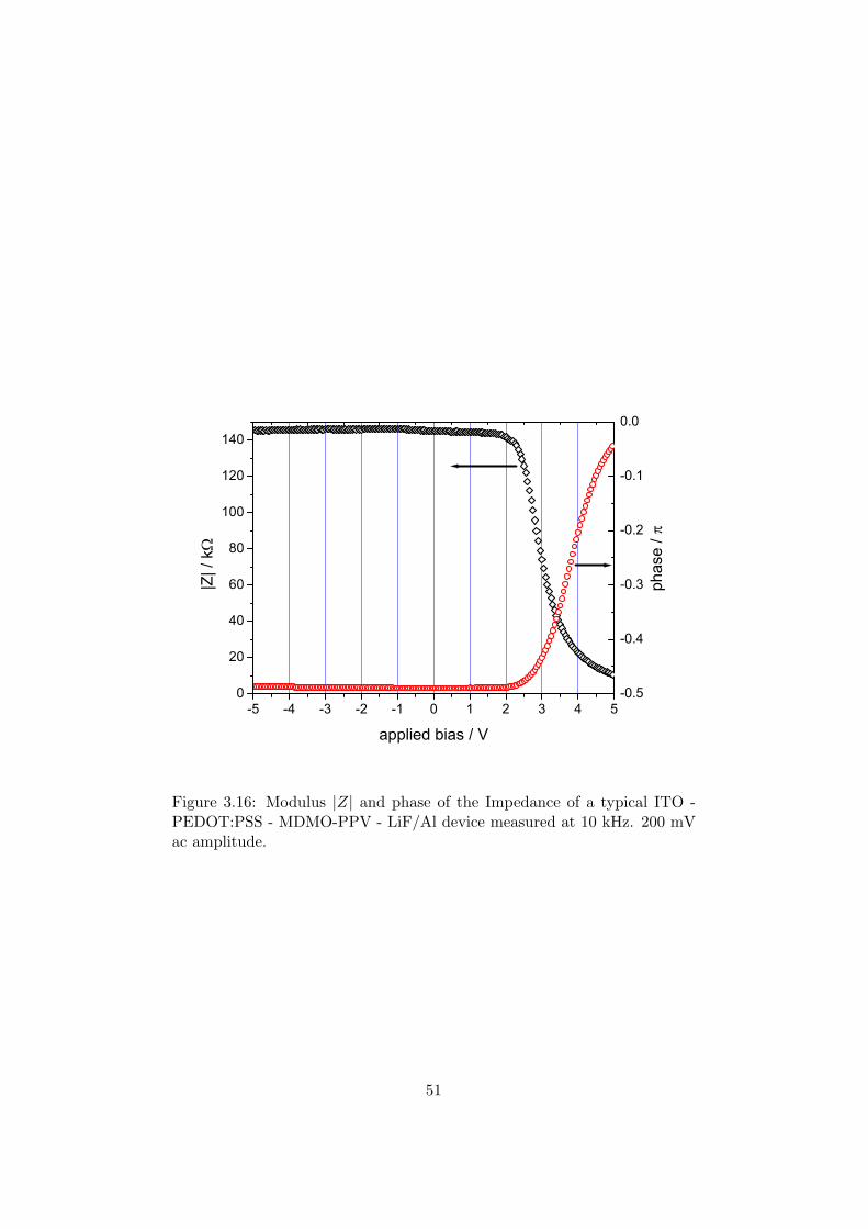
3.2.1 Admittance studies on MDMO-PPV based diodes
Figure 3.17 shows a set of capacitances for a typical ITO - PEDOT:PSS -MDMO-PPV - Al device with an active layer thickness of approximately130 nm. The applied bias voltages are between +1.5 V and +7 V and thefrequencies for vac range from 1 kHz to 1 MHz. At voltages from +2 V to +5V, the capacitance is rising from ≈ 1 nF at 1 MHz up to around 1.25 nF at 1kHz, in the case of +1.5 V even beyond 1.3 nF. Upon increasing the bias from+1.5 V to +2 V a knee appears around 5 kHz. This feature becomes morepronounced at +3 V, where the capacitance plot forms a distinct minimum,shifting to higher frequencies as the voltage is increased. For +7 V, anadditional feature becomes visible in the studied frequency window, namelyan effect of decreasing capacitance towards the lower frequency edge: Thecapacitance reaches a maximum around 2 kHz and decreases steadily whilethe frequency is lowered to 1 kHz.Hence, three regimes are observed for typical ITO - PEDOT:PSS - MDMO-
52
100010000
1000001000000
12
34
56
7
1.0
1.1
1.2
1.3
capa
cita
nce
/ nF
frequency / Hz
applied bias / V
Figure 3.17: Capacitance of a typical ITO - PEDOT:PSS - MDMO-PPV(130 nm) - Al device at various applied bias voltages as a function of fre-quency (200 mV ac amplitude).
53
PPV - Al devices presented in Fig. 3.17:
• In the studied frequency range of 1 kHz up to 1 MHz, the capacitancechanges about 25%.
• For voltages of +2 V and above, a knee-like feature appears whichturns into a minimum in the capacitance plot. This minimum shiftsfrom ≈ 3 kHz in the case of +2 V to ≈ 70 kHz when +7 V are appliedto the device.
• In the case of +7 V, the maximum in the capacitance is reached at2 kHz and decreases abruptly at lower frequencies. This behaviorsignificantly differs from that observed other lower voltages, where thecapacitance reached its highest value at 1 kHz, the lowest frequencymeasured.
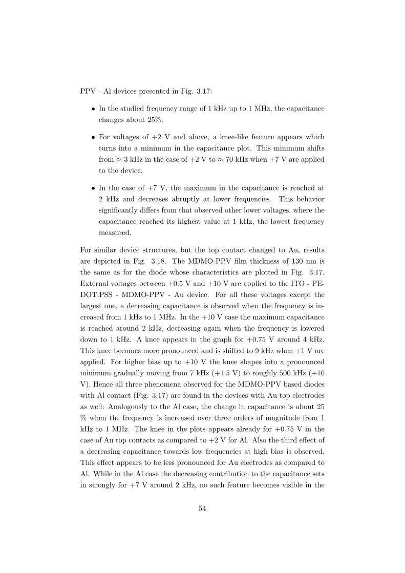
For similar device structures, but the top contact changed to Au, resultsare depicted in Fig. 3.18. The MDMO-PPV film thickness of 130 nm isthe same as for the diode whose characteristics are plotted in Fig. 3.17.External voltages between +0.5 V and +10 V are applied to the ITO - PE-DOT:PSS - MDMO-PPV - Au device. For all these voltages except thelargest one, a decreasing capacitance is observed when the frequency is in-creased from 1 kHz to 1 MHz. In the +10 V case the maximum capacitanceis reached around 2 kHz, decreasing again when the frequency is lowereddown to 1 kHz. A knee appears in the graph for +0.75 V around 4 kHz.This knee becomes more pronounced and is shifted to 9 kHz when +1 V areapplied. For higher bias up to +10 V the knee shapes into a pronouncedminimum gradually moving from 7 kHz (+1.5 V) to roughly 500 kHz (+10V). Hence all three phenomena observed for the MDMO-PPV based diodeswith Al contact (Fig. 3.17) are found in the devices with Au top electrodesas well: Analogously to the Al case, the change in capacitance is about 25% when the frequency is increased over three orders of magnitude from 1kHz to 1 MHz. The knee in the plots appears already for +0.75 V in thecase of Au top contacts as compared to +2 V for Al. Also the third effect ofa decreasing capacitance towards low frequencies at high bias is observed.This effect appears to be less pronounced for Au electrodes as compared toAl. While in the Al case the decreasing contribution to the capacitance setsin strongly for +7 V around 2 kHz, no such feature becomes visible in the
54
1000
10000
100000
1000000
0 1 2 3 4 5 6 7 8 9 10
1.2
1.3
1.4
1.5
1.6
frequency
/ Hz
capa
cita
nce
/ nF
applied bias / V
Figure 3.18: Capacitance of a typical ITO - PEDOT:PSS - MDMO-PPV(130 nm) - Au device at various applied bias voltages as a function of fre-quency (200 mV ac amplitude).
55
1001000
10000100000
1000000
1
2
3
4
-1.0
-0.5
0.0
0.5
1.0
1.5
capa
cita
nce
/ nF
frequency / Hz
applied bias / V
Figure 3.19: Capacitance of a typical ITO - PEDOT:PSS - MDMO-PPV(130 nm) - LiF/Al device in the frequency range 200 Hz to 1 MHz. Between+1.5 V and +4 V dc are externally applied. The ac amplitude is 200 mV.
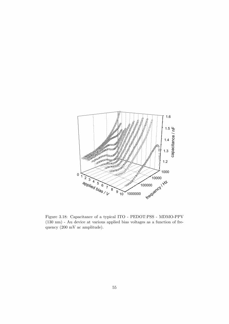
studied frequency range for Au top contacts for this voltage. Only at +10V a decreasing capacitance is observed in Fig. 3.18.
Figure 3.19 shows the measured device capacitance of a typical ITO -PEDOT:PSS - MDMO-PPV (130 nm) - LiF/Al structure in a voltage rangebetween +1.5 V and +4 V for frequencies between 200 Hz and 1 MHz. Thedata for the frequency scans were not taken in one shot but in several stages.It can be seen in Fig. 3.19 that these stages meet at 1 kHz and 2 kHz. Forthe two scans with the lowest applied bias of +1.5 V and +2 V an increas-ing capacitance with reducing frequency is observed in the studied range.Between 1 MHz and 1 kHz this increase is of the order of 25 %, hence beingcomparable to the two other cases of Al and Au top contacts shown above.This effect is not visible for the curves taken at higher voltages of +2.5 V,+3 V and +4 V. The capacitance in the scan at +2.5 V remains largely
56
independent of the frequency down to approximately 1 kHz. The +3 V scandeviates from the almost constant high frequency capacitance roughly below4 kHz, the +4 V scan already below 9 kHz. The distinct knees dominat-ing the medium to high frequency regime for the MDMO-PPV devices withAl and Au contacts (Figs. 3.17 and 3.18) cannot be observed for LiF/Altop electrodes. Instead, the mechanism which is reducing the capacitancetowards low frequencies is the dominating feature in all curves taken atvoltages more positive than +2 V. The effect is so pronounced that the ca-pacitance eventually turns negative around 230 Hz at +3 V and below 500Hz when +4 V are applied to the device.
3.2.2 Excess capacitance
For all data sets depicted in Figs. 3.17, 3.18 and 3.19 the capacitance reachesan almost stable value at the high frequency side. Although still slightlydecreasing, the influence of the above discussed phenomena appears to besmall. The geometric capacitance (Cg) of the studied devices is given by
Cg =εε0A
d, (3.2)
where ε0 is the permittivity of free space, ε the relative permittivity ofMDMO-PPV, A is the active surface area of the diode and d the thicknessof the MDMO-PPV films. For the actual devices presented above theseparameters are given by the device geometry (A = 5 - 6 mm2, d = 130nm) together with a typical ε for many conjugated polymers of 3 (e.g. [71])and ε0 = 8.85× 10⁻¹² Fm−1. With these values, the geometric capacitanceis calculated to be ≈ 1.0 nF - 1.2 nF. This is in excellent agreement withthe high frequency capacitances measured in the devices presented above.The increase in capacitance towards lower frequencies in the order of 25%has hence to be considered as excess capacitance exceeding the geometriccapacitance.
3.2.3 Single carrier drift mobility extracted from impedance
measurements
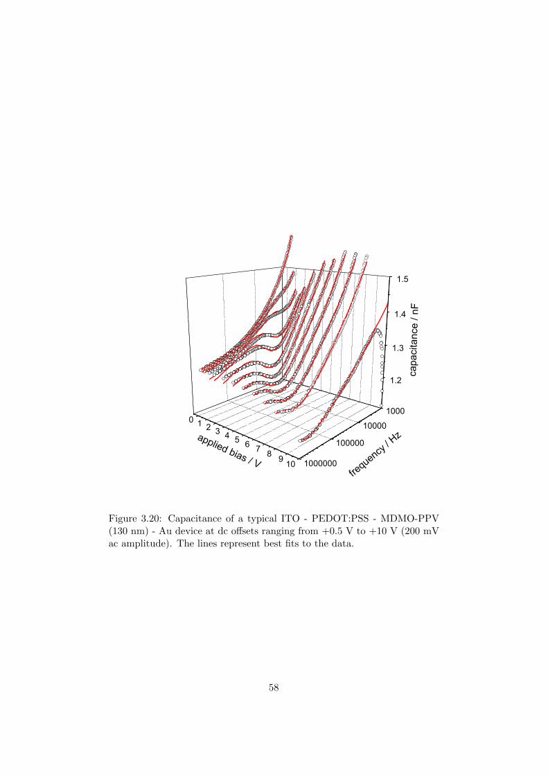
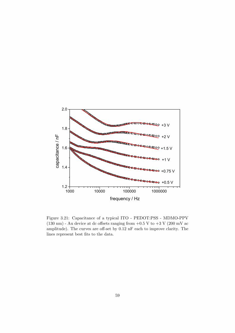
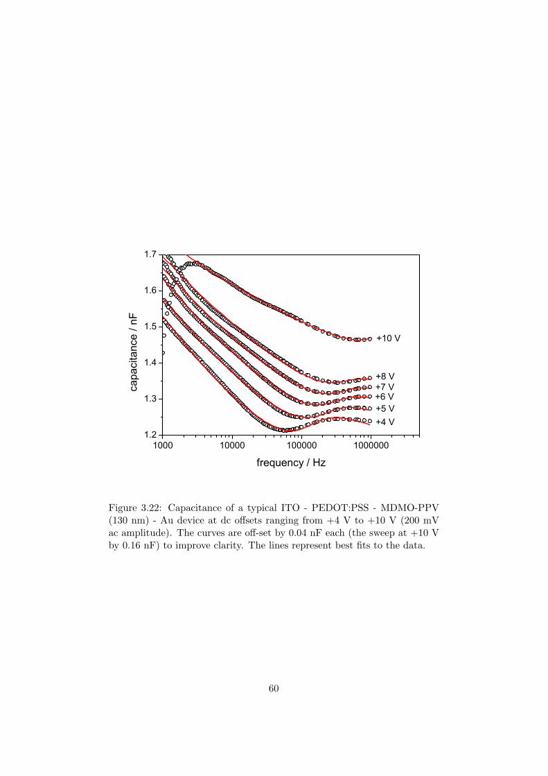
Figure 3.20 shows the measured capacitance of ITO - PEDOT:PSS - MDMO-PPV (130 nm) - Au diodes. It displays the same data as Fig. 3.18 together
57
1000
10000
100000
1000000
0 1 2 3 4 5 6 7 8 9 10
1.2
1.3
1.4
1.5
frequency
/ Hz
capa
cita
nce
/ nF
applied bias / V
Figure 3.20: Capacitance of a typical ITO - PEDOT:PSS - MDMO-PPV(130 nm) - Au device at dc offsets ranging from +0.5 V to +10 V (200 mVac amplitude). The lines represent best fits to the data.
58
1000 10000 100000 10000001.2
1.4
1.6
1.8
2.0
+3 V
+1 V
+2 V
+1.5 V
+0.75 V
+0.5 V
capa
cita
nce
/ nF
frequency / Hz
Figure 3.21: Capacitance of a typical ITO - PEDOT:PSS - MDMO-PPV(130 nm) - Au device at dc offsets ranging from +0.5 V to +3 V (200 mV acamplitude). The curves are off-set by 0.12 nF each to improve clarity. Thelines represent best fits to the data.
59
1000 10000 100000 10000001.2
1.3
1.4
1.5
1.6
1.7
+8 V
+10 V
+7 V+6 V+5 V+4 V
capa
cita
nce
/ nF
frequency / Hz
Figure 3.22: Capacitance of a typical ITO - PEDOT:PSS - MDMO-PPV(130 nm) - Au device at dc offsets ranging from +4 V to +10 V (200 mVac amplitude). The curves are off-set by 0.04 nF each (the sweep at +10 Vby 0.16 nF) to improve clarity. The lines represent best fits to the data.
60
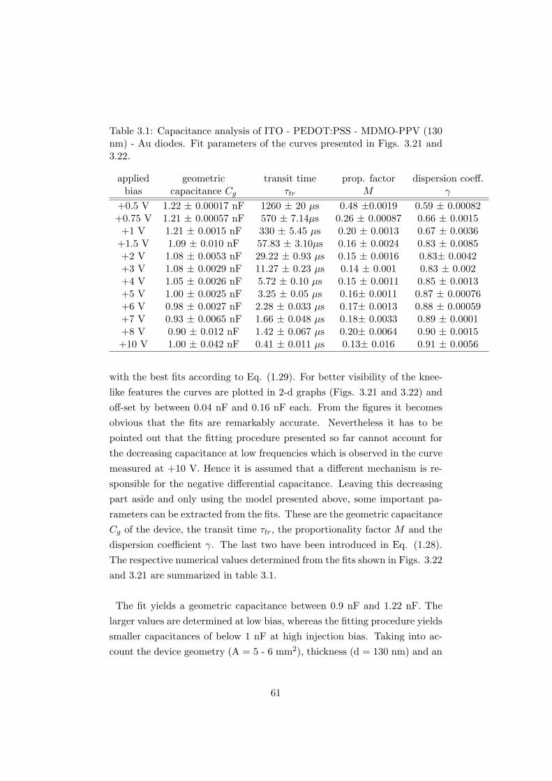
Table 3.1: Capacitance analysis of ITO - PEDOT:PSS - MDMO-PPV (130nm) - Au diodes. Fit parameters of the curves presented in Figs. 3.21 and3.22.
applied geometric transit time prop. factor dispersion coeff.bias capacitance Cg τtr M γ
+0.5 V 1.22 ± 0.00017 nF 1260 ± 20 µs 0.48 ±0.0019 0.59 ± 0.00082+0.75 V 1.21 ± 0.00057 nF 570 ± 7.14µs 0.26 ± 0.00087 0.66 ± 0.0015+1 V 1.21 ± 0.0015 nF 330 ± 5.45 µs 0.20 ± 0.0013 0.67 ± 0.0036
+1.5 V 1.09 ± 0.010 nF 57.83 ± 3.10µs 0.16 ± 0.0024 0.83 ± 0.0085+2 V 1.08 ± 0.0053 nF 29.22 ± 0.93 µs 0.15 ± 0.0016 0.83± 0.0042+3 V 1.08 ± 0.0029 nF 11.27 ± 0.23 µs 0.14 ± 0.001 0.83 ± 0.002+4 V 1.05 ± 0.0026 nF 5.72 ± 0.10 µs 0.15 ± 0.0011 0.85 ± 0.0013+5 V 1.00 ± 0.0025 nF 3.25 ± 0.05 µs 0.16± 0.0011 0.87 ± 0.00076+6 V 0.98 ± 0.0027 nF 2.28 ± 0.033 µs 0.17± 0.0013 0.88 ± 0.00059+7 V 0.93 ± 0.0065 nF 1.66 ± 0.048 µs 0.18± 0.0033 0.89 ± 0.0001+8 V 0.90 ± 0.012 nF 1.42 ± 0.067 µs 0.20± 0.0064 0.90 ± 0.0015+10 V 1.00 ± 0.042 nF 0.41 ± 0.011 µs 0.13± 0.016 0.91 ± 0.0056
with the best fits according to Eq. (1.29). For better visibility of the knee-like features the curves are plotted in 2-d graphs (Figs. 3.21 and 3.22) andoff-set by between 0.04 nF and 0.16 nF each. From the figures it becomesobvious that the fits are remarkably accurate. Nevertheless it has to bepointed out that the fitting procedure presented so far cannot account forthe decreasing capacitance at low frequencies which is observed in the curvemeasured at +10 V. Hence it is assumed that a different mechanism is re-sponsible for the negative differential capacitance. Leaving this decreasingpart aside and only using the model presented above, some important pa-rameters can be extracted from the fits. These are the geometric capacitanceCg of the device, the transit time τtr, the proportionality factor M and thedispersion coefficient γ. The last two have been introduced in Eq. (1.28).The respective numerical values determined from the fits shown in Figs. 3.22and 3.21 are summarized in table 3.1.
The fit yields a geometric capacitance between 0.9 nF and 1.22 nF. Thelarger values are determined at low bias, whereas the fitting procedure yieldssmaller capacitances of below 1 nF at high injection bias. Taking into ac-count the device geometry (A = 5 - 6 mm2), thickness (d = 130 nm) and an
61
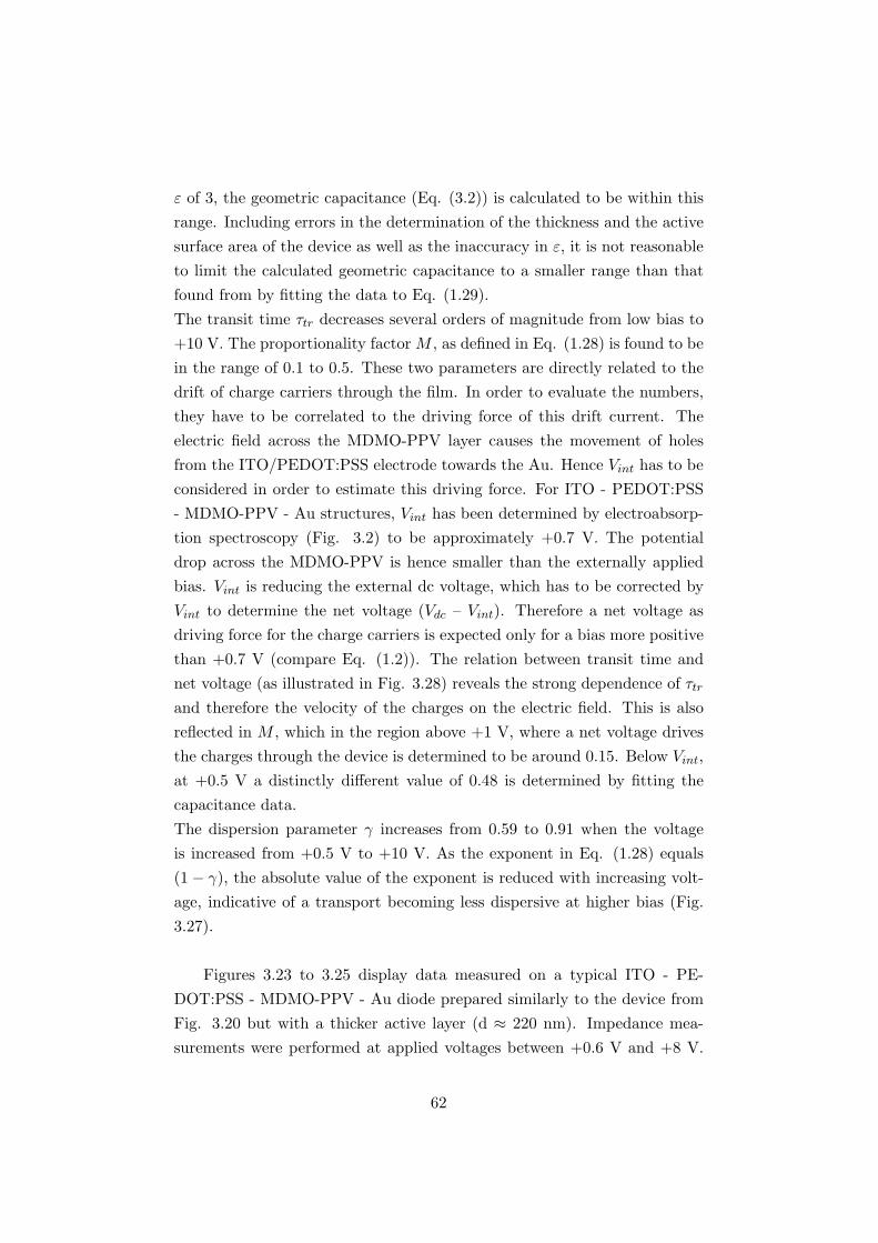
ε of 3, the geometric capacitance (Eq. (3.2)) is calculated to be within thisrange. Including errors in the determination of the thickness and the activesurface area of the device as well as the inaccuracy in ε, it is not reasonableto limit the calculated geometric capacitance to a smaller range than thatfound from by fitting the data to Eq. (1.29).The transit time τtr decreases several orders of magnitude from low bias to+10 V. The proportionality factor M , as defined in Eq. (1.28) is found to bein the range of 0.1 to 0.5. These two parameters are directly related to thedrift of charge carriers through the film. In order to evaluate the numbers,they have to be correlated to the driving force of this drift current. Theelectric field across the MDMO-PPV layer causes the movement of holesfrom the ITO/PEDOT:PSS electrode towards the Au. Hence Vint has to beconsidered in order to estimate this driving force. For ITO - PEDOT:PSS- MDMO-PPV - Au structures, Vint has been determined by electroabsorp-tion spectroscopy (Fig. 3.2) to be approximately +0.7 V. The potentialdrop across the MDMO-PPV is hence smaller than the externally appliedbias. Vint is reducing the external dc voltage, which has to be corrected byVint to determine the net voltage (Vdc – Vint). Therefore a net voltage asdriving force for the charge carriers is expected only for a bias more positivethan +0.7 V (compare Eq. (1.2)). The relation between transit time andnet voltage (as illustrated in Fig. 3.28) reveals the strong dependence of τtr
and therefore the velocity of the charges on the electric field. This is alsoreflected in M , which in the region above +1 V, where a net voltage drivesthe charges through the device is determined to be around 0.15. Below Vint,at +0.5 V a distinctly different value of 0.48 is determined by fitting thecapacitance data.The dispersion parameter γ increases from 0.59 to 0.91 when the voltageis increased from +0.5 V to +10 V. As the exponent in Eq. (1.28) equals(1− γ), the absolute value of the exponent is reduced with increasing volt-age, indicative of a transport becoming less dispersive at higher bias (Fig.3.27).
Figures 3.23 to 3.25 display data measured on a typical ITO - PE-DOT:PSS - MDMO-PPV - Au diode prepared similarly to the device fromFig. 3.20 but with a thicker active layer (d ≈ 220 nm). Impedance mea-surements were performed at applied voltages between +0.6 V and +8 V.
62
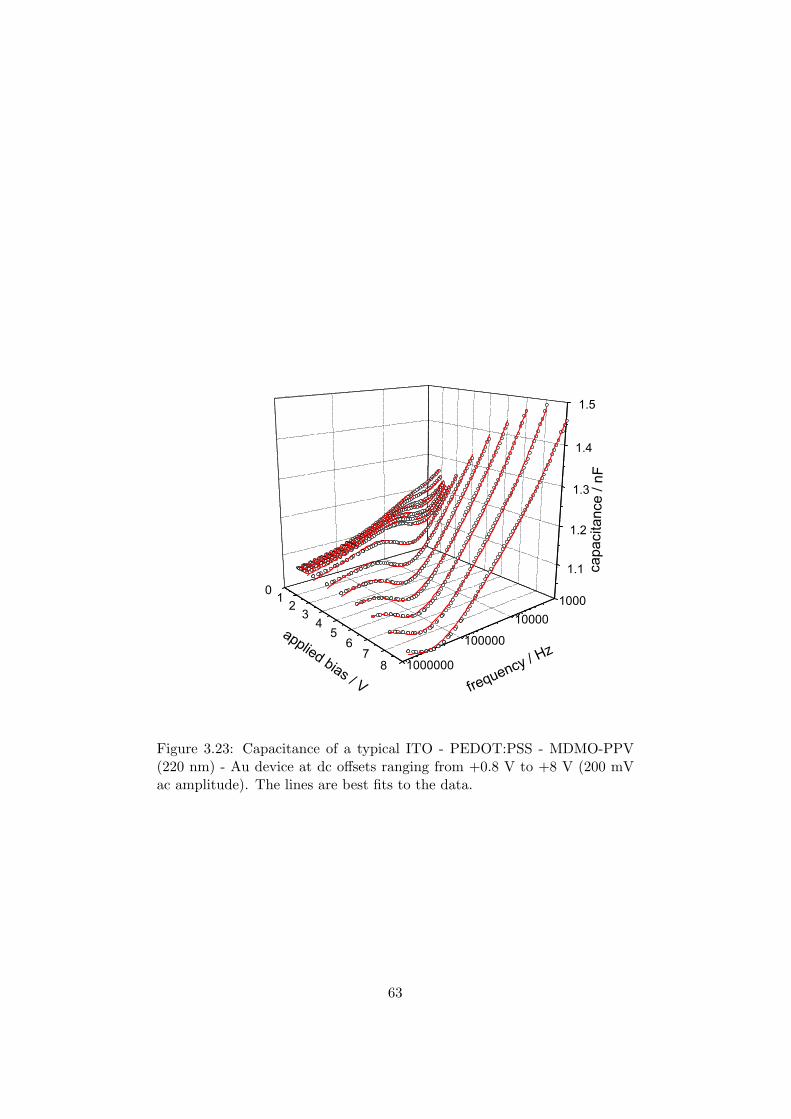
100010000
100000
1000000
0 1 23
45
67
8
1.1
1.2
1.3
1.4
1.5
frequency / Hz
capa
cita
nce
/ nF
applied bias / V
Figure 3.23: Capacitance of a typical ITO - PEDOT:PSS - MDMO-PPV(220 nm) - Au device at dc offsets ranging from +0.8 V to +8 V (200 mVac amplitude). The lines are best fits to the data.
63
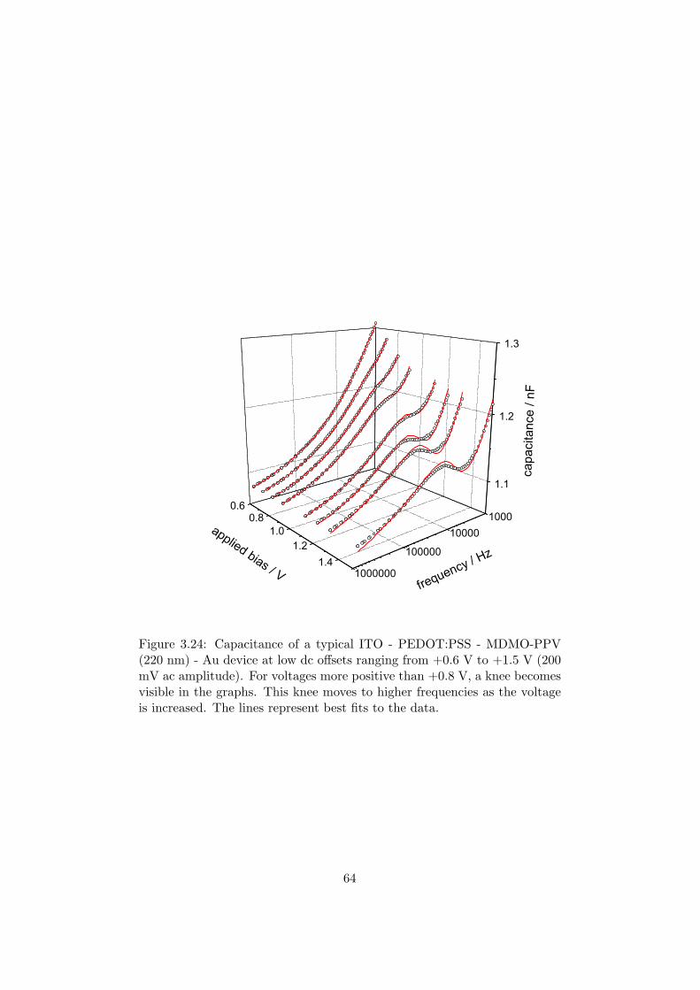
100010000
100000
1000000
0.60.8
1.01.2
1.4
1.1
1.2
1.3
frequency / Hz
capa
cita
nce
/ nF
applied bias / V
Figure 3.24: Capacitance of a typical ITO - PEDOT:PSS - MDMO-PPV(220 nm) - Au device at low dc offsets ranging from +0.6 V to +1.5 V (200mV ac amplitude). For voltages more positive than +0.8 V, a knee becomesvisible in the graphs. This knee moves to higher frequencies as the voltageis increased. The lines represent best fits to the data.
64
1000 10000 100000 1000000
1.1
1.2
1.3
1.4
1.5
+1.5 V
+1.3 V
+1.2 V
+1.1 V
+0.9 V
+0.8 V
+0.7 V
+0.6 V
capa
cita
nce
/ nF
frequency / Hz
Figure 3.25: Capacitance of a typical ITO - PEDOT:PSS - MDMO-PPV(220 nm) - Au device at low dc offsets ranging from +0.6 V to +1.5 V (200mV ac amplitude). Each sweep is off-set by 0.04 nF to the following. Forvoltages more positive than +0.8 V, a knee becomes visible in the graphs.This knee moves to higher frequencies as the voltage is increased. The linesrepresent best fits to the data.
65
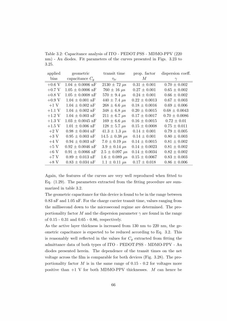
Table 3.2: Capacitance analysis of ITO - PEDOT:PSS - MDMO-PPV (220nm) - Au diodes. Fit parameters of the curves presented in Figs. 3.23 to3.25.
applied geometric transit time prop. factor dispersion coeff.bias capacitance Cg τtr M γ
+0.6 V 1.04 ± 0.0006 nF 2130 ± 72 µs 0.31 ± 0.001 0.70 ± 0.002+0.7 V 1.05 ± 0.0006 nF 760 ± 16 µs 0.27 ± 0.001 0.65 ± 0.002+0.8 V 1.05 ± 0.0008 nF 570 ± 9.4 µs 0.24 ± 0.001 0.66 ± 0.002+0.9 V 1.04 ± 0.001 nF 440 ± 7.4 µs 0.22 ± 0.0013 0.67 ± 0.003+1 V 1.04 ± 0.002 nF 268 ± 6.6 µs 0.18 ± 0.0016 0.69 ± 0.006
+1.1 V 1.04 ± 0.002 nF 348 ± 6.8 µs 0.20 ± 0.0015 0.68 ± 0.0043+1.2 V 1.04 ± 0.003 nF 211 ± 6.7 µs 0.17 ± 0.0017 0.70 ± 0.0086+1.3 V 1.03 ± 0.0045 nF 169 ± 6.6 µs 0.16 ± 0.0015 0.72 ± 0.01+1.5 V 1.01 ± 0.006 nF 128 ± 5.7 µs 0.15 ± 0.0008 0.75 ± 0.011+2 V 0.98 ± 0.004 nF 41.3 ± 1.3 µs 0.14 ± 0.001 0.79 ± 0.005+3 V 0.95 ± 0.003 nF 14.5 ± 0.38 µs 0.14 ± 0.001 0.80 ± 0.003+4 V 0.94 ± 0.003 nF 7.0 ± 0.19 µs 0.14 ± 0.0015 0.81 ± 0.002+5 V 0.92 ± 0.0046 nF 3.9 ± 0.14 µs 0.14 ± 0.0023 0.81 ± 0.002+6 V 0.91 ± 0.0066 nF 2.5 ± 0.097 µs 0.14 ± 0.0034 0.82 ± 0.002+7 V 0.89 ± 0.013 nF 1.6 ± 0.089 µs 0.15 ± 0.0067 0.83 ± 0.003+8 V 0.83 ± 0.034 nF 1.1 ± 0.11 µs 0.17 ± 0.018 0.86 ± 0.006
Again, the features of the curves are very well reproduced when fitted toEq. (1.29). The parameters extracted from the fitting procedure are sum-marized in table 3.2.The geometric capacitance for this device is found to be in the range between0.83 nF and 1.05 nF. For the charge carrier transit time, values ranging fromthe millisecond down to the microsecond regime are determined. The pro-portionality factor M and the dispersion parameter γ are found in the rangeof 0.15 - 0.31 and 0.65 - 0.86, respectively.As the active layer thickness is increased from 130 nm to 220 nm, the ge-ometric capacitance is expected to be reduced according to Eq. 3.2. Thisis reasonably well reflected in the values for Cg extracted from fitting theadmittance data of both types of ITO - PEDOT:PSS - MDMO-PPV - Audiodes presented herein. The dependence of the transit times on the netvoltage across the film is comparable for both devices (Fig. 3.28). The pro-portionality factor M is in the same range of 0.15 - 0.2 for voltages morepositive than +1 V for both MDMO-PPV thicknesses. M can hence be
66
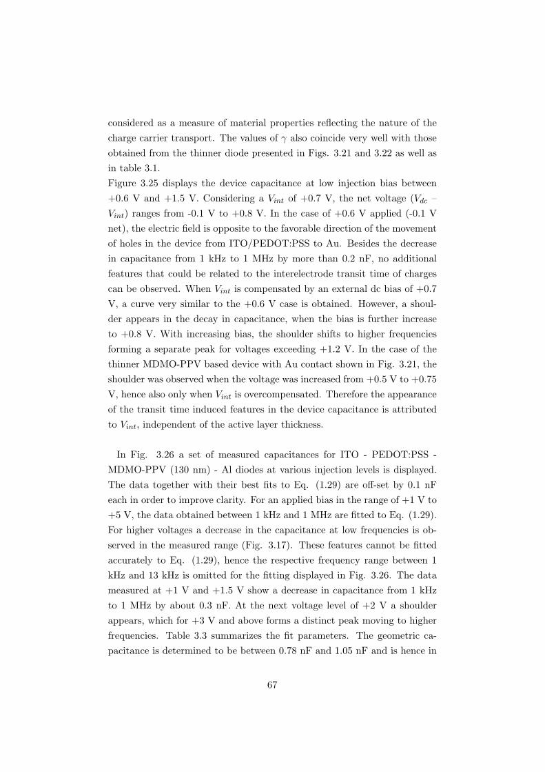
considered as a measure of material properties reflecting the nature of thecharge carrier transport. The values of γ also coincide very well with thoseobtained from the thinner diode presented in Figs. 3.21 and 3.22 as well asin table 3.1.Figure 3.25 displays the device capacitance at low injection bias between+0.6 V and +1.5 V. Considering a Vint of +0.7 V, the net voltage (Vdc –Vint) ranges from -0.1 V to +0.8 V. In the case of +0.6 V applied (-0.1 Vnet), the electric field is opposite to the favorable direction of the movementof holes in the device from ITO/PEDOT:PSS to Au. Besides the decreasein capacitance from 1 kHz to 1 MHz by more than 0.2 nF, no additionalfeatures that could be related to the interelectrode transit time of chargescan be observed. When Vint is compensated by an external dc bias of +0.7V, a curve very similar to the +0.6 V case is obtained. However, a shoul-der appears in the decay in capacitance, when the bias is further increaseto +0.8 V. With increasing bias, the shoulder shifts to higher frequenciesforming a separate peak for voltages exceeding +1.2 V. In the case of thethinner MDMO-PPV based device with Au contact shown in Fig. 3.21, theshoulder was observed when the voltage was increased from +0.5 V to +0.75V, hence also only when Vint is overcompensated. Therefore the appearanceof the transit time induced features in the device capacitance is attributedto Vint, independent of the active layer thickness.
In Fig. 3.26 a set of measured capacitances for ITO - PEDOT:PSS -MDMO-PPV (130 nm) - Al diodes at various injection levels is displayed.The data together with their best fits to Eq. (1.29) are off-set by 0.1 nFeach in order to improve clarity. For an applied bias in the range of +1 V to+5 V, the data obtained between 1 kHz and 1 MHz are fitted to Eq. (1.29).For higher voltages a decrease in the capacitance at low frequencies is ob-served in the measured range (Fig. 3.17). These features cannot be fittedaccurately to Eq. (1.29), hence the respective frequency range between 1kHz and 13 kHz is omitted for the fitting displayed in Fig. 3.26. The datameasured at +1 V and +1.5 V show a decrease in capacitance from 1 kHzto 1 MHz by about 0.3 nF. At the next voltage level of +2 V a shoulderappears, which for +3 V and above forms a distinct peak moving to higherfrequencies. Table 3.3 summarizes the fit parameters. The geometric ca-pacitance is determined to be between 0.78 nF and 1.05 nF and is hence in
67
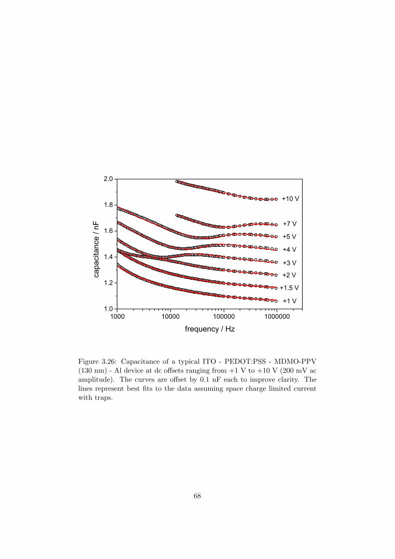
1000 10000 100000 10000001.0
1.2
1.4
1.6
1.8
2.0
+5 V
+1 V
+1.5 V
+2 V
+3 V
+4 V
+7 V
+10 V
capa
cita
nce
/ nF
frequency / Hz
Figure 3.26: Capacitance of a typical ITO - PEDOT:PSS - MDMO-PPV(130 nm) - Al device at dc offsets ranging from +1 V to +10 V (200 mV acamplitude). The curves are offset by 0.1 nF each to improve clarity. Thelines represent best fits to the data assuming space charge limited currentwith traps.
68
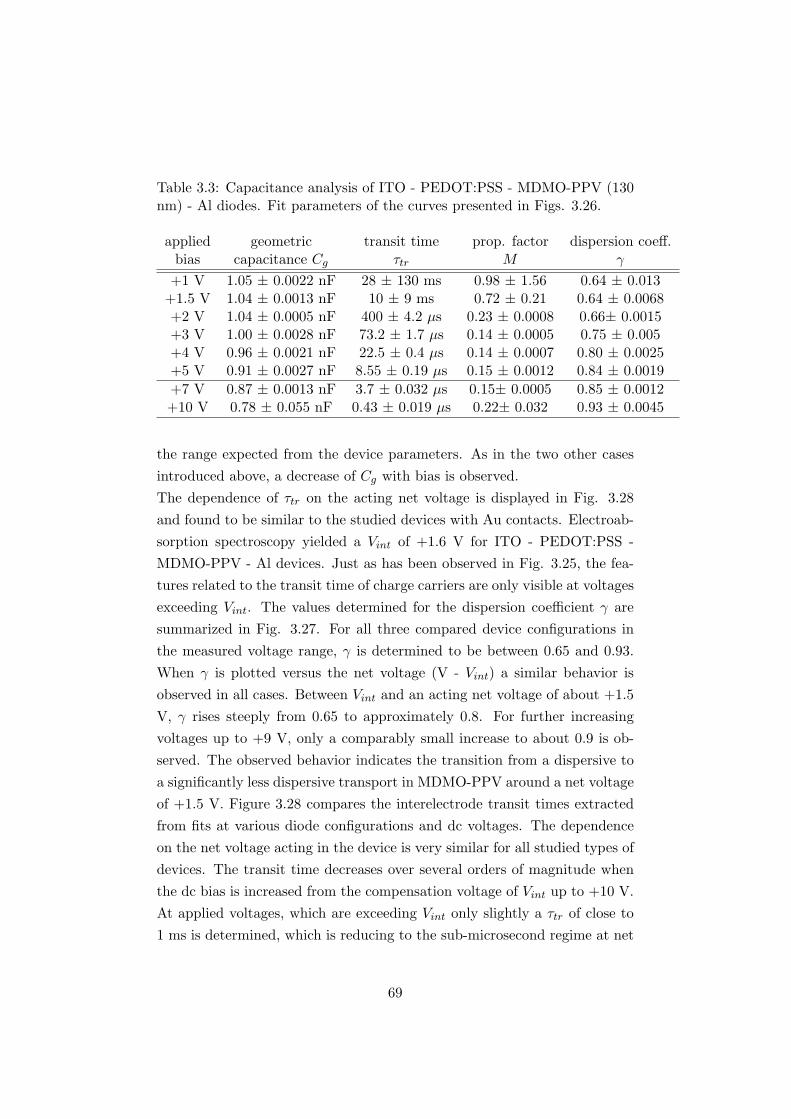
Table 3.3: Capacitance analysis of ITO - PEDOT:PSS - MDMO-PPV (130nm) - Al diodes. Fit parameters of the curves presented in Figs. 3.26.
applied geometric transit time prop. factor dispersion coeff.bias capacitance Cg τtr M γ
+1 V 1.05 ± 0.0022 nF 28 ± 130 ms 0.98 ± 1.56 0.64 ± 0.013+1.5 V 1.04 ± 0.0013 nF 10 ± 9 ms 0.72 ± 0.21 0.64 ± 0.0068+2 V 1.04 ± 0.0005 nF 400 ± 4.2 µs 0.23 ± 0.0008 0.66± 0.0015+3 V 1.00 ± 0.0028 nF 73.2 ± 1.7 µs 0.14 ± 0.0005 0.75 ± 0.005+4 V 0.96 ± 0.0021 nF 22.5 ± 0.4 µs 0.14 ± 0.0007 0.80 ± 0.0025+5 V 0.91 ± 0.0027 nF 8.55 ± 0.19 µs 0.15 ± 0.0012 0.84 ± 0.0019+7 V 0.87 ± 0.0013 nF 3.7 ± 0.032 µs 0.15± 0.0005 0.85 ± 0.0012+10 V 0.78 ± 0.055 nF 0.43 ± 0.019 µs 0.22± 0.032 0.93 ± 0.0045
the range expected from the device parameters. As in the two other casesintroduced above, a decrease of Cg with bias is observed.The dependence of τtr on the acting net voltage is displayed in Fig. 3.28and found to be similar to the studied devices with Au contacts. Electroab-sorption spectroscopy yielded a Vint of +1.6 V for ITO - PEDOT:PSS -MDMO-PPV - Al devices. Just as has been observed in Fig. 3.25, the fea-tures related to the transit time of charge carriers are only visible at voltagesexceeding Vint. The values determined for the dispersion coefficient γ aresummarized in Fig. 3.27. For all three compared device configurations inthe measured voltage range, γ is determined to be between 0.65 and 0.93.When γ is plotted versus the net voltage (V - Vint) a similar behavior isobserved in all cases. Between Vint and an acting net voltage of about +1.5V, γ rises steeply from 0.65 to approximately 0.8. For further increasingvoltages up to +9 V, only a comparably small increase to about 0.9 is ob-served. The observed behavior indicates the transition from a dispersive toa significantly less dispersive transport in MDMO-PPV around a net voltageof +1.5 V. Figure 3.28 compares the interelectrode transit times extractedfrom fits at various diode configurations and dc voltages. The dependenceon the net voltage acting in the device is very similar for all studied types ofdevices. The transit time decreases over several orders of magnitude whenthe dc bias is increased from the compensation voltage of Vint up to +10 V.At applied voltages, which are exceeding Vint only slightly a τtr of close to1 ms is determined, which is reducing to the sub-microsecond regime at net
69
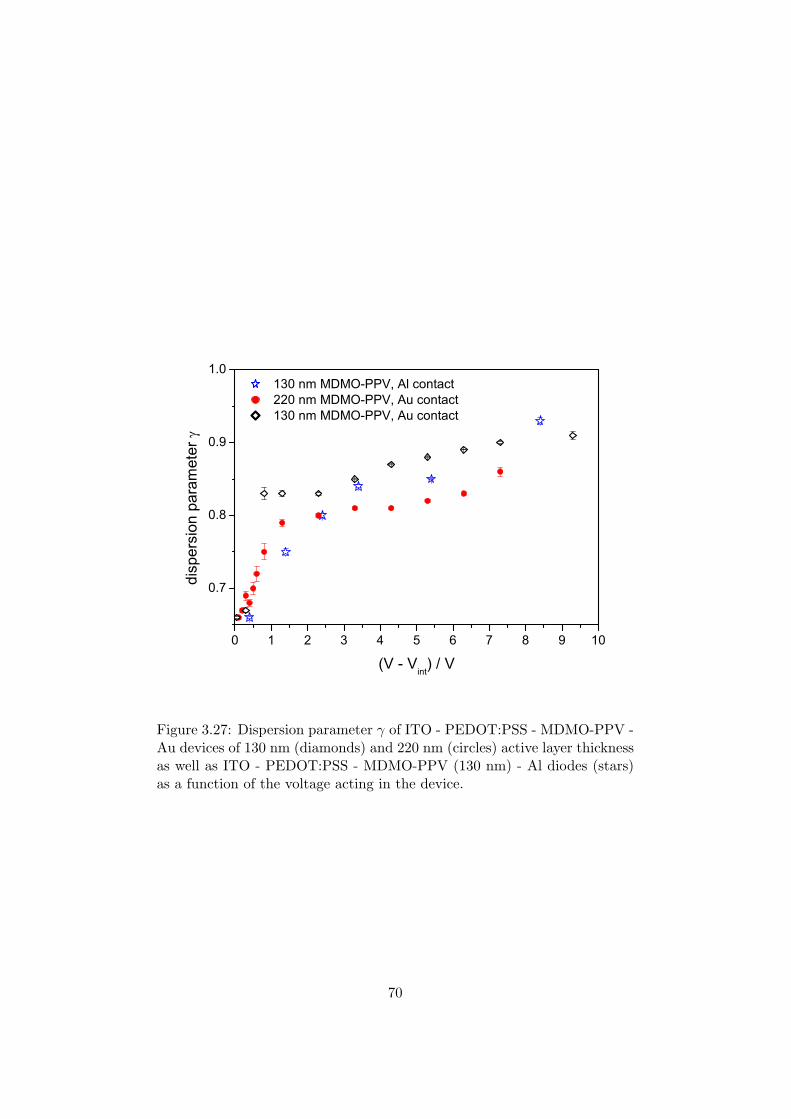
0 1 2 3 4 5 6 7 8 9 10
0.7
0.8
0.9
1.0 130 nm MDMO-PPV, Al contact 220 nm MDMO-PPV, Au contact 130 nm MDMO-PPV, Au contact
disp
ersi
on p
aram
eter
(V - Vint
) / V
Figure 3.27: Dispersion parameter γ of ITO - PEDOT:PSS - MDMO-PPV -Au devices of 130 nm (diamonds) and 220 nm (circles) active layer thicknessas well as ITO - PEDOT:PSS - MDMO-PPV (130 nm) - Al diodes (stars)as a function of the voltage acting in the device.
70
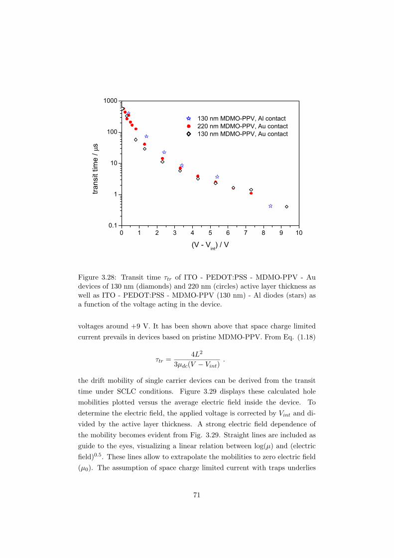
0 1 2 3 4 5 6 7 8 9 100.1
1
10
100
1000
130 nm MDMO-PPV, Al contact 220 nm MDMO-PPV, Au contact 130 nm MDMO-PPV, Au contact
trans
it tim
e /
s
(V - Vint
) / V
Figure 3.28: Transit time τtr of ITO - PEDOT:PSS - MDMO-PPV - Audevices of 130 nm (diamonds) and 220 nm (circles) active layer thickness aswell as ITO - PEDOT:PSS - MDMO-PPV (130 nm) - Al diodes (stars) asa function of the voltage acting in the device.
voltages around +9 V. It has been shown above that space charge limitedcurrent prevails in devices based on pristine MDMO-PPV. From Eq. (1.18)
τtr =4L2
3µdc(V − Vint).
the drift mobility of single carrier devices can be derived from the transittime under SCLC conditions. Figure 3.29 displays these calculated holemobilities plotted versus the average electric field inside the device. Todetermine the electric field, the applied voltage is corrected by Vint and di-vided by the active layer thickness. A strong electric field dependence ofthe mobility becomes evident from Fig. 3.29. Straight lines are included asguide to the eyes, visualizing a linear relation between log(µ) and (electricfield)0.5. These lines allow to extrapolate the mobilities to zero electric field(µ0). The assumption of space charge limited current with traps underlies
71
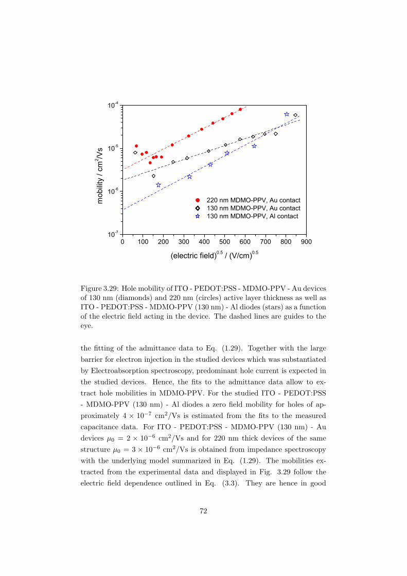
0 100 200 300 400 500 600 700 800 90010-7
10-6
10-5
10-4
220 nm MDMO-PPV, Au contact 130 nm MDMO-PPV, Au contact 130 nm MDMO-PPV, Al contact
mob
ility
/ cm
2 /Vs
(electric field)0.5 / (V/cm)0.5
Figure 3.29: Hole mobility of ITO - PEDOT:PSS - MDMO-PPV - Au devicesof 130 nm (diamonds) and 220 nm (circles) active layer thickness as well asITO - PEDOT:PSS - MDMO-PPV (130 nm) - Al diodes (stars) as a functionof the electric field acting in the device. The dashed lines are guides to theeye.
the fitting of the admittance data to Eq. (1.29). Together with the largebarrier for electron injection in the studied devices which was substantiatedby Electroabsorption spectroscopy, predominant hole current is expected inthe studied devices. Hence, the fits to the admittance data allow to ex-tract hole mobilities in MDMO-PPV. For the studied ITO - PEDOT:PSS- MDMO-PPV (130 nm) - Al diodes a zero field mobility for holes of ap-proximately 4 × 10⁻⁷ cm2/Vs is estimated from the fits to the measuredcapacitance data. For ITO - PEDOT:PSS - MDMO-PPV (130 nm) - Audevices µ0 = 2 × 10⁻⁶ cm2/Vs and for 220 nm thick devices of the samestructure µ0 = 3 × 10⁻⁶ cm2/Vs is obtained from impedance spectroscopywith the underlying model summarized in Eq. (1.29). The mobilities ex-tracted from the experimental data and displayed in Fig. 3.29 follow theelectric field dependence outlined in Eq. (3.3). They are hence in good
72
agreement with the findings reported in the literature. Also the numericalvalues of the zero field hole mobilities estimated from Fig. 3.29, which aredetermined to be in the order of 10−6 cm2/Vs are in line with previouslypublished values [46, 41, 30]. PPV derivatives are well studied compoundsin the field of polymer semiconductors. Reflecting this importance, chargecarrier mobilities in PPVs and especially MDMO-PPV have been derivedin a whole variety of different ways (e.g. [41, 46, 30]). The electric fielddependence of the mobility of various PPV derivatives was found to be welldescribed by the stretched (”Poole-Frenkel type” [72]) exponential law [73]
µ(E) = µ0 exp(γF
√E) . (3.3)
Here, µ0 is the zero-field mobility, while γF describes the ”field activation”of the mobility. The mobility relation described in Eq. (3.3) has been foundin a whole variety of different materials ([74] and references herein), startingwith poly(N-vinyl carbazole) already 30 years ago [75, 31]. Also more recenttime-of-flight (ToF) experiments yield the same dependence [76]. Basslerdeveloped a model based on Monte Carlo simulation [11]. Though muchmore elaborate than Eq. (3.3) it yields the same proportionality betweenthe mobility and E (µ ∝ exp
√E). This peculiar relation stems from the
fact that barriers for charge transport in the field direction by the appliedelectrostatic potential [77].
3.3 Negative capacitance
3.3.1 Negative capacitance in MDMO-PPV based diodes
By fitting the experimental admittance data to Eq. (1.29) good results canbe achieved as shown in the previous section. For moderate injection intoMDMO-PPV based diodes with electrodes yielding an appreciable barrierfor electron injection (Au, Al), the agreement is excellent. However, with in-creasing forward bias a phenomenon becomes visible which is not accountedfor in the fit (e.g. Fig. 3.20): In the low frequency range a mechanism whichdiminishes the measured capacitance is observed. This effect is becomingincreasingly pronounced when the top electrode is changed from Au to Al(Fig. 3.26). For LiF/Al electrodes it is already dominating the admittancedata (Fig. 3.19), even causing the capacitance to change sign at low frequen-
73
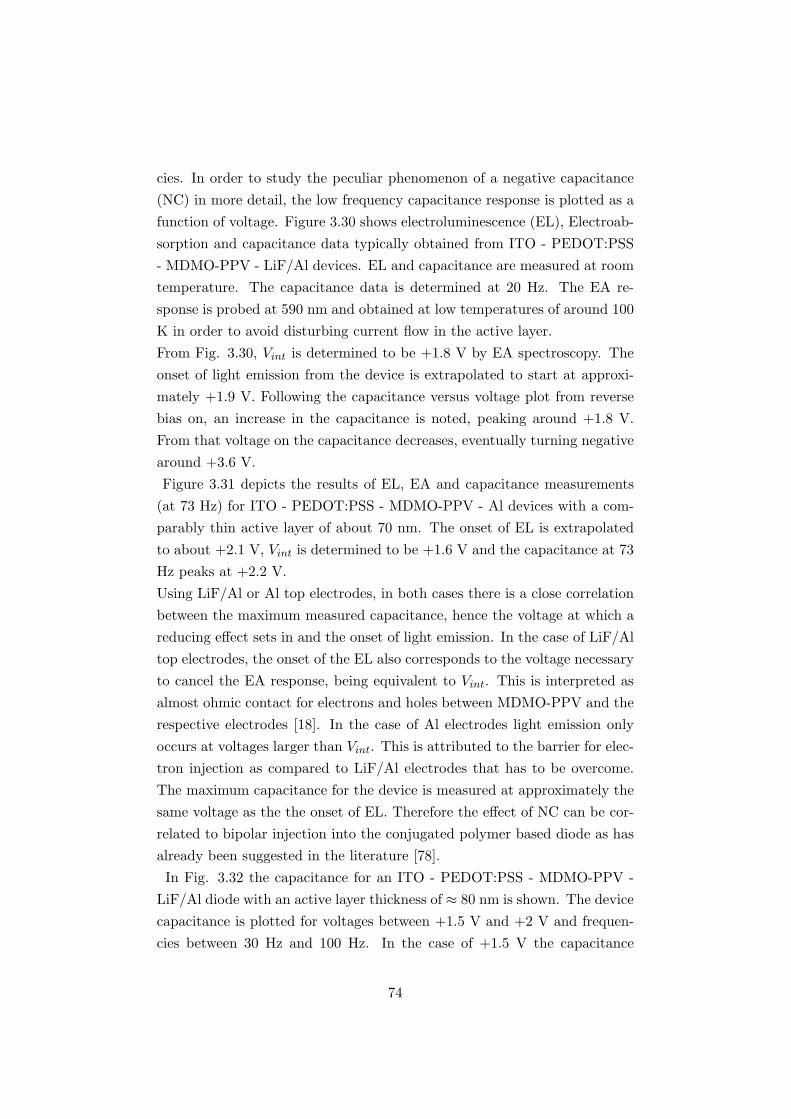
cies. In order to study the peculiar phenomenon of a negative capacitance(NC) in more detail, the low frequency capacitance response is plotted as afunction of voltage. Figure 3.30 shows electroluminescence (EL), Electroab-sorption and capacitance data typically obtained from ITO - PEDOT:PSS- MDMO-PPV - LiF/Al devices. EL and capacitance are measured at roomtemperature. The capacitance data is determined at 20 Hz. The EA re-sponse is probed at 590 nm and obtained at low temperatures of around 100K in order to avoid disturbing current flow in the active layer.From Fig. 3.30, Vint is determined to be +1.8 V by EA spectroscopy. Theonset of light emission from the device is extrapolated to start at approxi-mately +1.9 V. Following the capacitance versus voltage plot from reversebias on, an increase in the capacitance is noted, peaking around +1.8 V.From that voltage on the capacitance decreases, eventually turning negativearound +3.6 V.Figure 3.31 depicts the results of EL, EA and capacitance measurements
(at 73 Hz) for ITO - PEDOT:PSS - MDMO-PPV - Al devices with a com-parably thin active layer of about 70 nm. The onset of EL is extrapolatedto about +2.1 V, Vint is determined to be +1.6 V and the capacitance at 73Hz peaks at +2.2 V.Using LiF/Al or Al top electrodes, in both cases there is a close correlationbetween the maximum measured capacitance, hence the voltage at which areducing effect sets in and the onset of light emission. In the case of LiF/Altop electrodes, the onset of the EL also corresponds to the voltage necessaryto cancel the EA response, being equivalent to Vint. This is interpreted asalmost ohmic contact for electrons and holes between MDMO-PPV and therespective electrodes [18]. In the case of Al electrodes light emission onlyoccurs at voltages larger than Vint. This is attributed to the barrier for elec-tron injection as compared to LiF/Al electrodes that has to be overcome.The maximum capacitance for the device is measured at approximately thesame voltage as the the onset of EL. Therefore the effect of NC can be cor-related to bipolar injection into the conjugated polymer based diode as hasalready been suggested in the literature [78].In Fig. 3.32 the capacitance for an ITO - PEDOT:PSS - MDMO-PPV -
LiF/Al diode with an active layer thickness of ≈ 80 nm is shown. The devicecapacitance is plotted for voltages between +1.5 V and +2 V and frequen-cies between 30 Hz and 100 Hz. In the case of +1.5 V the capacitance
74
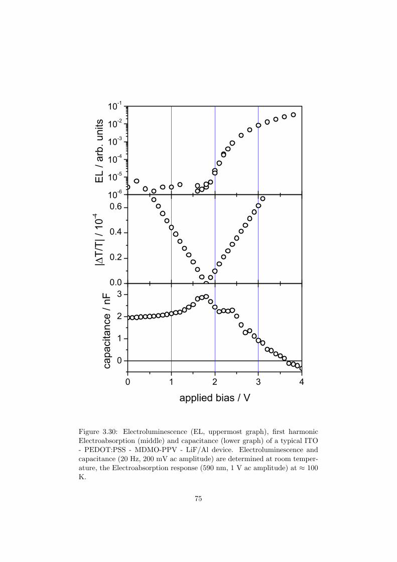
0 1 2 3 4
0
1
2
30.0
0.2
0.4
0.610-6
10-5
10-4
10-3
10-2
10-1
applied bias / V
capa
cita
nce
/ nF
|T/
T| /
10-4
EL
/ arb
. uni
ts
Figure 3.30: Electroluminescence (EL, uppermost graph), first harmonicElectroabsorption (middle) and capacitance (lower graph) of a typical ITO- PEDOT:PSS - MDMO-PPV - LiF/Al device. Electroluminescence andcapacitance (20 Hz, 200 mV ac amplitude) are determined at room temper-ature, the Electroabsorption response (590 nm, 1 V ac amplitude) at ≈ 100K.
75
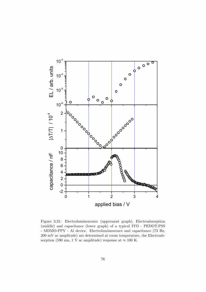
0 1 2 3 4-202468
100
1
2
10-6
10-5
10-4
10-3
capa
cita
nce
/ nF
applied bias / V
|T/
T| /
10-4
EL
/ arb
. uni
ts
Figure 3.31: Electroluminescence (uppermost graph), Electroabsorption(middle) and capacitance (lower graph) of a typical ITO - PEDOT:PSS- MDMO-PPV - Al device. Electroluminescence and capacitance (73 Hz,200 mV ac amplitude) are determined at room temperature, the Electroab-sorption (590 nm, 1 V ac amplitude) response at ≈ 100 K.
76
1002.0
2.5
3.0
3.5
+ 2.0 V
+ 1.9 V
+ 1.5 V+ 1.8 V+ 1.7 V
90807040 50 6030
capa
cita
nce
/ nF
frequency / Hz
Figure 3.32: Capacitance of ITO - PEDOT:PSS - MDMO-PPV (≈ 80 nm)- LiF/Al devices at frequencies ranging from 30 Hz to 100 Hz. Applied biasbetween +1.5 V and +2 V.
77
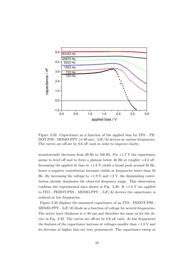
0.0 0.5 1.0 1.5 2.0 2.5 3.0-1.0
0.0
1.0
2.0
3.0
4.0
5.0 83333 Hz20870 Hz2023 Hz1023 Hz723 Hz123 Hz
capa
cita
nce
/ nF
applied bias / V
Figure 3.33: Capacitance as a function of the applied bias for ITO - PE-DOT:PSS - MDMO-PPV (≈ 80 nm) - LiF/Al devices at various frequencies.The curves are off-set by 0.6 nF each in order to improve clarity.
monotonously decreases from 30 Hz to 100 Hz. For +1.7 V the capacitanceseems to level off and to form a plateau below 40 Hz at roughly +3.2 nF.Increasing the applied dc bias to +1.8 V yields a broad peak around 50 Hz,hence a negative contribution becomes visible at frequencies lower than 50Hz. By increasing the voltage to +1.9 V and +2 V, the diminishing contri-bution already dominates the observed frequency range. This observationconfirms the experimental data shown in Fig. 3.30. If +1.8 V are appliedto ITO - PEDOT:PSS - MDMO-PPV - LiF/Al devices the capacitance isreduced at low frequencies.Figure 3.33 displays the measured capacitance of an ITO - PEDOT:PSS -
MDMO-PPV - LiF/Al diode as a function of voltage for several frequencies.The active layer thickness is ≈ 80 nm and therefore the same as for the de-vice in Fig. 3.32. The curves are off-set by 0.6 nF each. At low frequenciesthe features of the capacitance increase at voltages smaller than +1.8 V andits decrease at higher bias are very pronounced. The capacitance sweep at
78
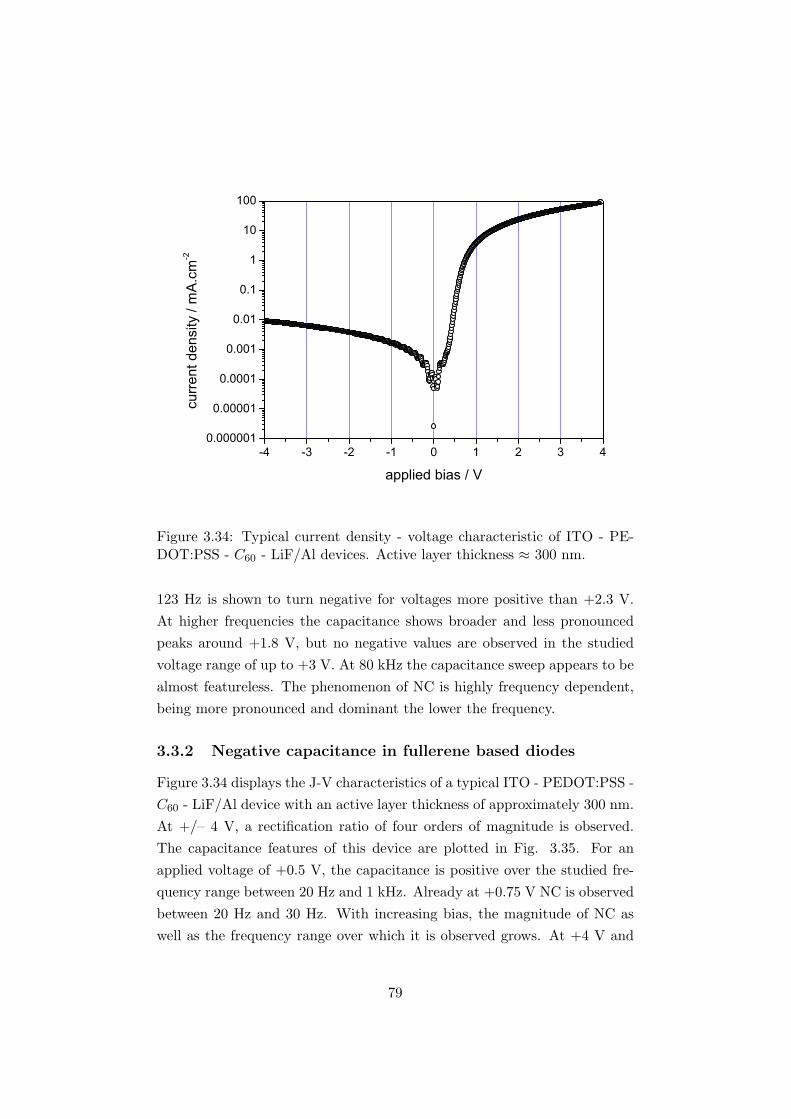
-4 -3 -2 -1 0 1 2 3 40.000001
0.00001
0.0001
0.001
0.01
0.1
1
10
100cu
rren
t den
sity
/ m
A.c
m-2
applied bias / V
Figure 3.34: Typical current density - voltage characteristic of ITO - PE-DOT:PSS - C60 - LiF/Al devices. Active layer thickness ≈ 300 nm.
123 Hz is shown to turn negative for voltages more positive than +2.3 V.At higher frequencies the capacitance shows broader and less pronouncedpeaks around +1.8 V, but no negative values are observed in the studiedvoltage range of up to +3 V. At 80 kHz the capacitance sweep appears to bealmost featureless. The phenomenon of NC is highly frequency dependent,being more pronounced and dominant the lower the frequency.
3.3.2 Negative capacitance in fullerene based diodes
Figure 3.34 displays the J-V characteristics of a typical ITO - PEDOT:PSS -C60 - LiF/Al device with an active layer thickness of approximately 300 nm.At +/– 4 V, a rectification ratio of four orders of magnitude is observed.The capacitance features of this device are plotted in Fig. 3.35. For anapplied voltage of +0.5 V, the capacitance is positive over the studied fre-quency range between 20 Hz and 1 kHz. Already at +0.75 V NC is observedbetween 20 Hz and 30 Hz. With increasing bias, the magnitude of NC aswell as the frequency range over which it is observed grows. At +4 V and
79
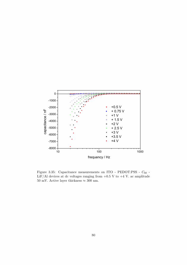
10 100 1000-8000
-7000
-6000
-5000
-4000
-3000
-2000
-1000
0
+0.5 V + 0.75 V +1 V + 1.5 V +2 V + 2.5 V +3 V +3.5 V +4 V
capa
cita
nce
/ nF
frequency / Hz
Figure 3.35: Capacitance measurements on ITO - PEDOT:PSS - C60 -LiF/Al devices at dc voltages ranging from +0.5 V to +4 V. ac amplitude50 mV. Active layer thickness ≈ 300 nm.
80
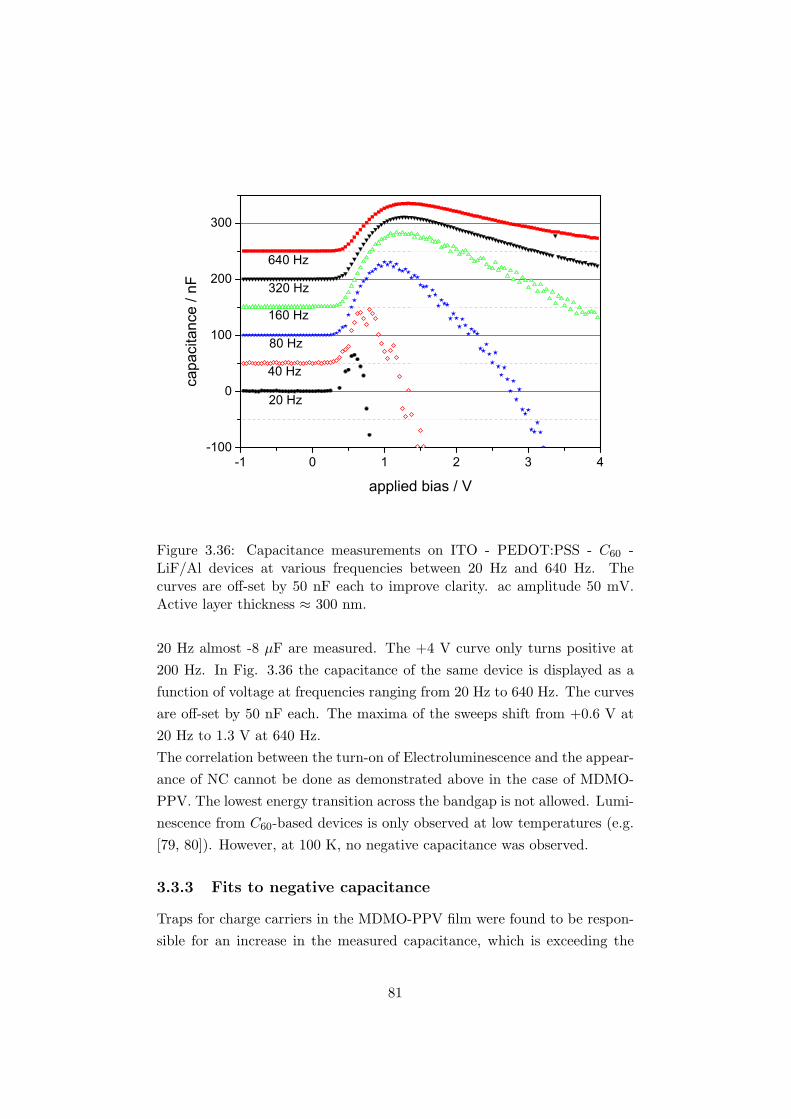
-1 0 1 2 3 4-100
0
100
200
300
40 Hz
80 Hz
160 Hz
320 Hz
640 Hz
20 Hz
capa
cita
nce
/ nF
applied bias / V
Figure 3.36: Capacitance measurements on ITO - PEDOT:PSS - C60 -LiF/Al devices at various frequencies between 20 Hz and 640 Hz. Thecurves are off-set by 50 nF each to improve clarity. ac amplitude 50 mV.Active layer thickness ≈ 300 nm.
20 Hz almost -8 µF are measured. The +4 V curve only turns positive at200 Hz. In Fig. 3.36 the capacitance of the same device is displayed as afunction of voltage at frequencies ranging from 20 Hz to 640 Hz. The curvesare off-set by 50 nF each. The maxima of the sweeps shift from +0.6 V at20 Hz to 1.3 V at 640 Hz.The correlation between the turn-on of Electroluminescence and the appear-ance of NC cannot be done as demonstrated above in the case of MDMO-PPV. The lowest energy transition across the bandgap is not allowed. Lumi-nescence from C60-based devices is only observed at low temperatures (e.g.[79, 80]). However, at 100 K, no negative capacitance was observed.
3.3.3 Fits to negative capacitance
Traps for charge carriers in the MDMO-PPV film were found to be respon-sible for an increase in the measured capacitance, which is exceeding the
81
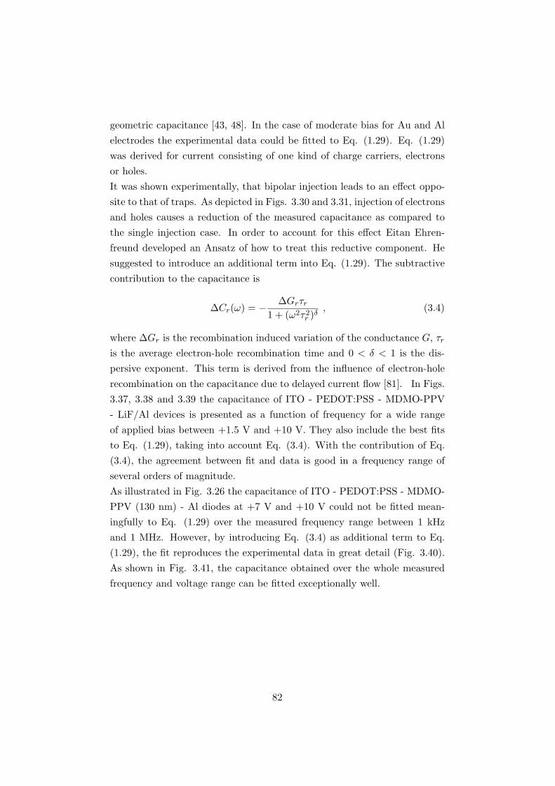
geometric capacitance [43, 48]. In the case of moderate bias for Au and Alelectrodes the experimental data could be fitted to Eq. (1.29). Eq. (1.29)was derived for current consisting of one kind of charge carriers, electronsor holes.It was shown experimentally, that bipolar injection leads to an effect oppo-site to that of traps. As depicted in Figs. 3.30 and 3.31, injection of electronsand holes causes a reduction of the measured capacitance as compared tothe single injection case. In order to account for this effect Eitan Ehren-freund developed an Ansatz of how to treat this reductive component. Hesuggested to introduce an additional term into Eq. (1.29). The subtractivecontribution to the capacitance is
∆Cr(ω) = − ∆Grτr
1 + (ω2τ2r )δ
, (3.4)
where ∆Gr is the recombination induced variation of the conductance G, τr
is the average electron-hole recombination time and 0 < δ < 1 is the dis-persive exponent. This term is derived from the influence of electron-holerecombination on the capacitance due to delayed current flow [81]. In Figs.3.37, 3.38 and 3.39 the capacitance of ITO - PEDOT:PSS - MDMO-PPV- LiF/Al devices is presented as a function of frequency for a wide rangeof applied bias between +1.5 V and +10 V. They also include the best fitsto Eq. (1.29), taking into account Eq. (3.4). With the contribution of Eq.(3.4), the agreement between fit and data is good in a frequency range ofseveral orders of magnitude.As illustrated in Fig. 3.26 the capacitance of ITO - PEDOT:PSS - MDMO-PPV (130 nm) - Al diodes at +7 V and +10 V could not be fitted mean-ingfully to Eq. (1.29) over the measured frequency range between 1 kHzand 1 MHz. However, by introducing Eq. (3.4) as additional term to Eq.(1.29), the fit reproduces the experimental data in great detail (Fig. 3.40).As shown in Fig. 3.41, the capacitance obtained over the whole measuredfrequency and voltage range can be fitted exceptionally well.
82
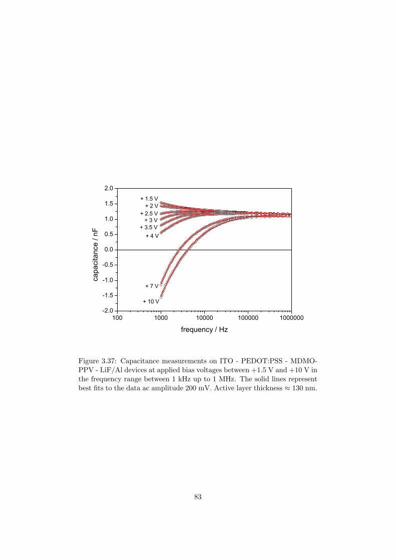
100 1000 10000 100000 1000000-2.0
-1.5
-1.0
-0.5
0.0
0.5
1.0
1.5
2.0
+ 1.5 V+ 2 V
+ 2.5 V+ 3 V
+ 3.5 V+ 4 V
+ 7 V
+ 10 V
capa
cita
nce
/ nF
frequency / Hz
Figure 3.37: Capacitance measurements on ITO - PEDOT:PSS - MDMO-PPV - LiF/Al devices at applied bias voltages between +1.5 V and +10 V inthe frequency range between 1 kHz up to 1 MHz. The solid lines representbest fits to the data ac amplitude 200 mV. Active layer thickness ≈ 130 nm.
83
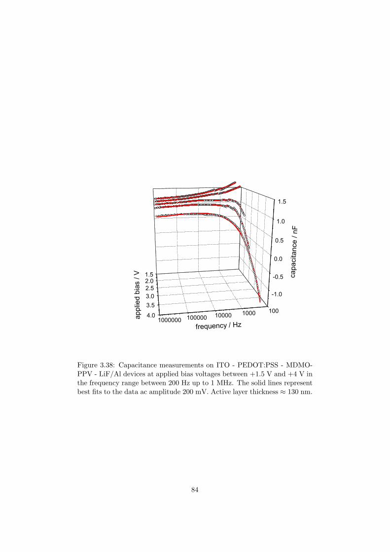
1001000100001000001000000
1.52.02.53.03.5
4.0
-1.0
-0.5
0.0
0.5
1.0
1.5
capa
cita
nce
/ nF
frequency / Hz
appl
ied
bias
/ V
Figure 3.38: Capacitance measurements on ITO - PEDOT:PSS - MDMO-PPV - LiF/Al devices at applied bias voltages between +1.5 V and +4 V inthe frequency range between 200 Hz up to 1 MHz. The solid lines representbest fits to the data ac amplitude 200 mV. Active layer thickness ≈ 130 nm.
84
10 100 1000 10000 100000 1000000-140
-120
-100
-80
-60
-40
-20
0
capa
cita
nce
/ nF
frequency / Hz
Figure 3.39: Capacitance measurements on ITO - PEDOT:PSS - MDMO-PPV - LiF/Al devices at +10 V from 20 Hz up to 1 MHz. The solid linerepresents the best fit to the data. ac amplitude 200 mV. Active layerthickness ≈ 130 nm.
85
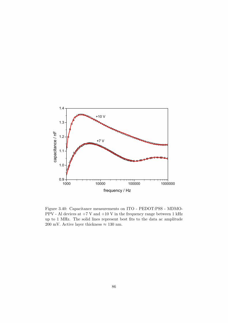
1000 10000 100000 10000000.9
1.0
1.1
1.2
1.3
1.4
+7 V
+10 V
capa
cita
nce
/ nF
frequency / Hz
Figure 3.40: Capacitance measurements on ITO - PEDOT:PSS - MDMO-PPV - Al devices at +7 V and +10 V in the frequency range between 1 kHzup to 1 MHz. The solid lines represent best fits to the data ac amplitude200 mV. Active layer thickness ≈ 130 nm.
86
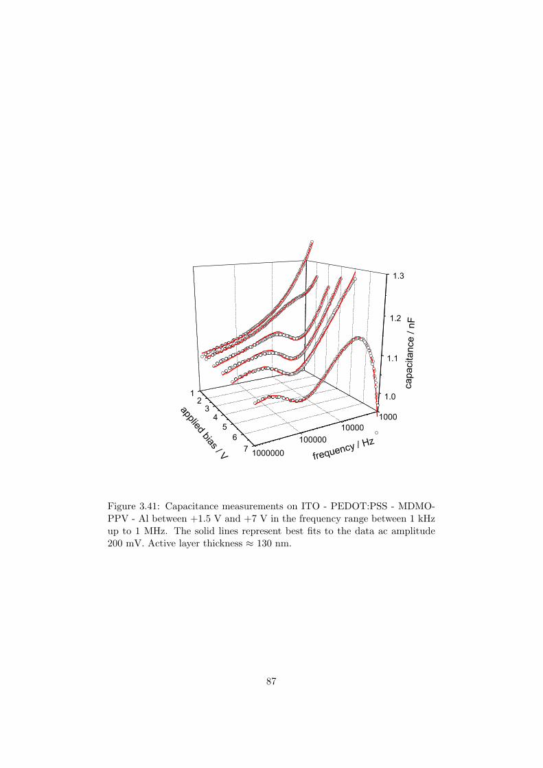
100010000
1000001000000
12
34
56
7
1.0
1.1
1.2
1.3
capa
cita
nce
/ nF
frequency / Hz
applied bias / V
Figure 3.41: Capacitance measurements on ITO - PEDOT:PSS - MDMO-PPV - Al between +1.5 V and +7 V in the frequency range between 1 kHzup to 1 MHz. The solid lines represent best fits to the data ac amplitude200 mV. Active layer thickness ≈ 130 nm.
87
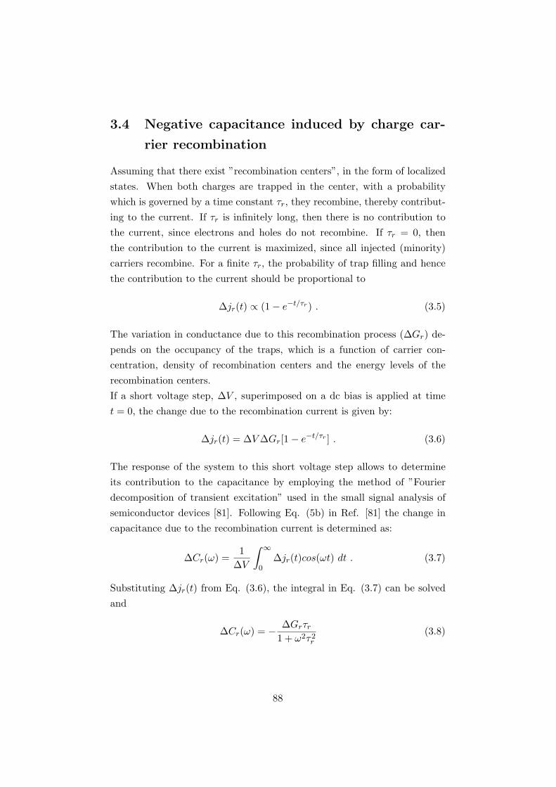
3.4 Negative capacitance induced by charge car-
rier recombination
Assuming that there exist ”recombination centers”, in the form of localizedstates. When both charges are trapped in the center, with a probabilitywhich is governed by a time constant τr, they recombine, thereby contribut-ing to the current. If τr is infinitely long, then there is no contribution tothe current, since electrons and holes do not recombine. If τr = 0, thenthe contribution to the current is maximized, since all injected (minority)carriers recombine. For a finite τr, the probability of trap filling and hencethe contribution to the current should be proportional to
∆jr(t) ∝ (1− e−t/τr) . (3.5)
The variation in conductance due to this recombination process (∆Gr) de-pends on the occupancy of the traps, which is a function of carrier con-centration, density of recombination centers and the energy levels of therecombination centers.If a short voltage step, ∆V , superimposed on a dc bias is applied at timet = 0, the change due to the recombination current is given by:
∆jr(t) = ∆V ∆Gr[1− e−t/τr ] . (3.6)
The response of the system to this short voltage step allows to determineits contribution to the capacitance by employing the method of ”Fourierdecomposition of transient excitation” used in the small signal analysis ofsemiconductor devices [81]. Following Eq. (5b) in Ref. [81] the change incapacitance due to the recombination current is determined as:
∆Cr(ω) =1
∆V
∫ ∞
0∆jr(t)cos(ωt) dt . (3.7)
Substituting ∆jr(t) from Eq. (3.6), the integral in Eq. (3.7) can be solvedand
∆Cr(ω) = − ∆Grτr
1 + ω2τ2r
(3.8)
88
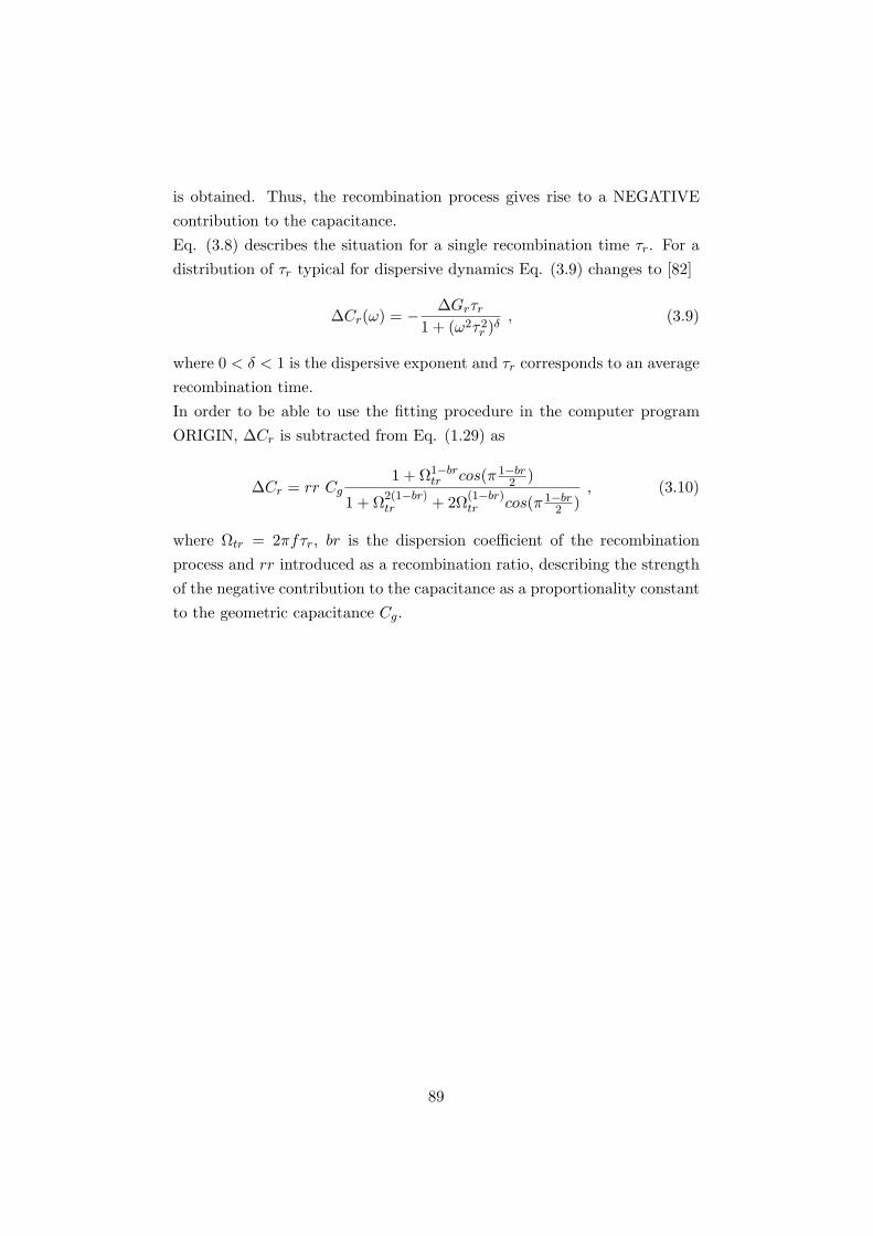
is obtained. Thus, the recombination process gives rise to a NEGATIVEcontribution to the capacitance.Eq. (3.8) describes the situation for a single recombination time τr. For adistribution of τr typical for dispersive dynamics Eq. (3.9) changes to [82]
∆Cr(ω) = − ∆Grτr
1 + (ω2τ2r )δ
, (3.9)
where 0 < δ < 1 is the dispersive exponent and τr corresponds to an averagerecombination time.In order to be able to use the fitting procedure in the computer programORIGIN, ∆Cr is subtracted from Eq. (1.29) as
∆Cr = rr Cg1 + Ω1−br
tr cos(π 1−br2 )
1 + Ω2(1−br)tr + 2Ω(1−br)
tr cos(π 1−br2 )
, (3.10)
where Ωtr = 2πfτr, br is the dispersion coefficient of the recombinationprocess and rr introduced as a recombination ratio, describing the strengthof the negative contribution to the capacitance as a proportionality constantto the geometric capacitance Cg.
89
Chapter 4
Conclusion
The internal electric field in organic semiconductor thin film devices basedon π-conjugated polymers is determined and the implications of Vint on thedevice performance is studied. Vint is identified as the maximum photovolt-age theoretically deliverable by the respective device. It is determined tobe the driving force of the photocurrent and depends on the metal top con-tact in the case of pristine polymer devices. However, Vint was shown to bechanged by adding only 1 % (w/w) of an electron acceptor species (PCBM).In this case evidence was found that Vint is determined by the energy offsetbetween the HOMO of MDMO-PPV and the LUMO of PCBM.With a sufficiently small amount of mobile charge carriers, which was shownto be the case for MDMO-PPV in the dark, the electric field is homogeneousin absence of significant charge carrier injection. However, in doped con-jugated polymers, such as P3HT exposed to air, the amount of free chargecarriers in the film is sufficient to screen the electric field already close to theelectrode. In this case, Schottky-like behavior of the semiconductor/metalcontact was demonstrated.From the determination of Vint, a substantial barrier for electron injectionfrom Al and Au contacts into MDMO-PPV is apparent. Dominant hole cur-rent at sufficiently small voltages is hence concluded. Underlying a modelbased on single carrier space charge limited current with traps, the measuredadmittance could be fitted satisfactorily for moderate bias.At higher voltages or by using LiF/Al electrodes, a negative contribution tothe device capacitance was found experimentally and could be correlated tobipolar injection. At sufficiently large bias and low frequencies this feature is
90

dominant and can result in a measured negative device capacitance. In orderto account for this contribution, an additional term has to be introduced tothe established fit formalism in order to achieve reasonable agreement withthe experimental data. This negative contribution is derived assuming aslow recombination process between electrons and holes.
91
Bibliography
[1] W. Helfich and W. G. Schneider. Phys. Rev. Lett., 14:226, 1965.
[2] G. H. Heilmeier and S. E. Harrison. Phys. Rev., 132, 1963.
[3] C. W. Tang and S. A. VanSlyke. Appl. Phys. Lett., 51:913, 1987.
[4] H. Shirakawa, E. J. Louis, A. G. MacDiarmid, C. K. Chiang, and A. J.Heeger. J. Chem. Soc. Chem. Comm., 16:578, 1977.
[5] C. K. Chiang, C. R. Fincher Jr, Y. W. Park, A. J. Heeger, E. J. LouisH. Shirakawa, S. C. Gau, and A. G. MacDiarmid. Phys. Rev. Lett.,39(17):1098, 1977.
[6] C. K. Chiang, M. A. Druy, S. C. Gau, A. J. Heeger, E. J. Louis, A. G.MacDiarmid, Y. W. Park, and H. Shirakawa. J. Am. Chem. Soc.,100:1013, 1978.
[7] M. C. Scharber, D. Muhlbacher, M. Koppe, P. Denk, C. Waldauf, A. J.Heeger, and C. J. Brabec. Adv. Funct. Mat., 18:789, 2006.
[8] W. Brutting, S. Berleb, and A. G. Muckl. Org. Electron., 2:1, 2001.
[9] S. M. Sze. Physics of semiconductor devices. John Wiley & Sons, NewYork, 1981.
[10] Primary photoexcitations in conjugated polymers: Molecular excitonversus semiconductor band model. Edited by N.S. Sariciftci, WorldScientific, Singapore, 1997.
[11] H. Bassler. Phys. Status Solidi (b), 175:15, 1993.
[12] P. Wurfel. Physics of Solar Cells. John Wiley & Sons, New York, 1997.
92
[13] C. Lungenschmied, G. Dennler, H. Neugebauer, N. S. Sariciftci,M. Glatthaar, T. Meyer, and A. Meyer. Sol. Energy Mater. Sol. Cells,91:379, 2007.
[14] L. J. A. Koster, V. D. Mihailetchi, and P. W. M. Blom. Appl. Phys.Lett., 88:093511, 2006.
[15] S. E. Shaheen, R. Radspinner, N. Peyghambarian, and G. E. Jabbour.Appl. Phys. Lett., 79:2996, 2001.
[16] M. A. Lampert and P. Mark. Current injection in solids. AcademicPress, New York, 1970.
[17] G. Dennler, N. S. Sariciftci, R. Schwodiauer, S. Bauer, and H. Reiss.Appl. Phys. Lett., 86:193507, 2005.
[18] C. Lungenschmied, G. Dennler, E. Ehrenfreund, H. Neugebauer, andN. S. Sariciftci. Appl. Phys. Lett., 89:223519, 2006.
[19] B. A. Mattis, P. C. Chang, and V. Subramanian. Mat. Res. Soc. Symp.Proc., 771, 2003.
[20] M. S. A. Abdou, F.P. Orfino, Y. Son, and S. Holdcroft. J. Am. Chem.Soc., 119:4518, 1997.
[21] S. Hoshino, M. Yoshida, S. Uemura, T. Kodzasa, N. Takada, T. Ka-mata, and K. Yase. J. Appl. Phys., 95:5088, 2004.
[22] N. S. Sariciftci, L. Smilowitz, A. J. Heeger, and F. Wudl. Science,258:1474, 1992.
[23] S. E. Shaheen, C. J. Brabec, F. Padinger, T. Fromherz, J. C. Humme-len, and N. S. Sariciftci. Appl. Phys. Lett., 78:841, 2001.
[24] I. H. Campbell, T. W. Hagler, D. L. Smith, and J. P. Ferraris. Phys.Rev. Lett., 76:1900, 1996.
[25] L. S. Hung, C. W. Tang, and M. G. Mason. Appl. Phys. Lett., 70:152,1997.
[26] T. M. Brown, R. H. Friend, I. S. Millard, D. L. Lacey, J. H. Burroughes,and F. Cacialli. Appl. Phys. Lett., 77(19):3096, 2000.
93
[27] T. M. Brown, R. H. Friend, I. S. Millard, D. L. Lacey, T. Butler, J. H.Burroughes, and F. Cacialli. J. Appl. Phys., 93(10):6159, 2003.
[28] C. Lungenschmied, G. Dennler, E. Ehrenfreund, H. Neugebauer, andN. S. Sariciftci. Proc. SPIE, 6192:322, 2006.
[29] I. D. Parker. J. Appl. Phys., 75(3):1656, 1994.
[30] H. C. F. Martens, P. W. M. Blom, and H. F. M. Schoo. Phys. Rev. B,61:7489, 2000.
[31] W. D. Gill. J. Appl. Phys., 43:5033, 1972.
[32] G. Yu, C. Zhang, and A. J. Heeger. Appl. Phys. Lett., 64:1540, 1994.
[33] C. J. Brabec, S. Shaheen, C. Winder, P. Denk, and N. S. Sariciftci.Appl. Phys. Lett., 80:1288, 2002.
[34] C. J. Brabec, A. Cravino, D. Meissner, N. S. Sariciftci, T. Fromherz,M.T. Rispens, L. Sanchez, and J.C. Hummelen. Adv. Funct. Mater.,11:374, 2001.
[35] A. Gadias, M. Svensson, M. Andersson, and O. Inganas. Appl. Phys.Lett., 84:1609, 2004.
[36] J. Liu, Y. Shi, and Y. Yang. Adv. Funct. Mater., 11:420, 2001.
[37] L. J. A. Koster, V. D. Mihailetchi, and P. W. M. Blom. Appl. Phys.Lett., 88:093511, 2006.
[38] G. J. Matt, N. S. Sariciftci, and T. Fromherz. Appl. Phys. Lett., 84:1570,2004.
[39] J. H. Burroughes, D. D. C. Bradley, A. R. Brown, R. N. Marks,K. Mackey, R. H. Friend, P. L. Burn, and A. B. Holmes. Nature,347:539, 1990.
[40] P. Stadler. Diploma Thesis, Johannes Kepler University, Linz, 2006.
[41] P. W. M. Blom, M. J. M. de Jong, and J. J. M. Vleggaar. Appl. Phys.Lett., 68:3308, 1996.
[42] I. Shao and G. T. Wright. Solid State Electronics, 3:291, 1961.
94
[43] R. Kassing. Phys. Status Solidi (a), 28:107, 1975.
[44] R. Kassing and E. Kahler. Solid State Commun., 15:673, 1974.
[45] P. W. M. Blom and M. C. J. M. Vissenberg. Phys. Rev. Lett., 80:3819,1998.
[46] G. Dennler, A. J. Mozer, G. Juska, A. Pivrikas, R. Osterbacka,A. Fuchsbauer, and N. S. Sariciftci. Org. Electron., 7:229, 2006.
[47] A. J. Mozer, N. S. Sariciftci, L. Lutsen, D. Vanderzande, R. Osterbacka,M. Westerling, and Juska. Appl. Phys. Lett., 86:112104, 2005.
[48] H. C. F. Martens, H. B. Brom, and P. W. M. Blom. Phys. Rev. B,60:R8489, 1999.
[49] J. Bisquert, G. Garcia-Belmonte, A. Pitarch, and H. Bolink. Chem.Phys. Lett., 422:184, 2006.
[50] S. Berleb and W. Brutting. Phys. Rev. Lett., 89:286601, 2001.
[51] H. H. P. Gommans, V. Kemerink, and R. A. J. Janssen. Phys. Rev. B,72:235204, 2005.
[52] A. Pitarch, G. Garcia-Belmonte, J. Bisquert, and H. Bolink. J. Appl.Phys., 100:084502, 2006.
[53] A. Pitarch, G. Garcia-Belmonte, and J. Bisquert. Proc. SPIE, 5519:307,2004.
[54] H. C. F. Martens, J. N. Huiberts, and P. W. M. Blom. Appl. Phys.Lett., 77:1852, 2000.
[55] H. H. P. Gommans, V. Kemerink, and W. H. A. Schilders. Phys. Rev.B, 72:165110, 2005.
[56] G. Weiser and A. Horvath. Primary photoexcitations in conjugatedpolymers: Molecular exciton versus semiconductor band model, chapter12, Electroabsorption spectroscopy on π-conjugated polymers. Editedby N.S. Sariciftci, World Scientific, Singapore, 1997.
[57] D. Muhlbacher, H. Neugebauer, A. Cravino, and N. S. Sariciftci. Synth.Met., 137:1361, 2003.
95
[58] V. D. Mihailetchi, P. W. D. Blom, J. C. Hummelen, and M. T. Rispens.J. Appl. Phys., 94:6849, 2003.
[59] A. Rajagopal, C. I. Wu, and A . Kahn. J. Appl. Phys, 83:2649, 1998.
[60] H. Ishii, K. Sugiyama, E. Ito, and K. Seki. Adv. Mat., 11:605, 1999.
[61] G. Dennler, C. Lungenschmied, N. S. Sariciftci, R. Schwodiauer,S. Bauer, and H. Reiss. Appl. Phys. Lett., 87:163501, 2005.
[62] A. Assadi, C. Svensson, M. Willander, and O. Inganas. J. Appl. Phys.,72:2900, 1992.
[63] M. Meier, S. Karg, and W. Riess. J. Appl. Phys., 82:1961, 1997.
[64] K. Henisch. Rectifying Semiconductor Contacts. Clarendon, Oxford,1957.
[65] S. Karg, M. Meier, and W. Riess. J. Appl. Phys., 82:1951, 1997.
[66] H. Tomozawa, D. Braun, S. D. Phillips, R. Worland, A. J. Heeger, andH. Kroemer. Synth. Metals, 28:687, 1989.
[67] Z. Chiguvare, J. Parisi, and V. Dyakonov. J. Appl. Phys., 94:2440,2003.
[68] H. Killesreiter and H. Baessler. Chem. Phys. Lett., 11:411, 1971.
[69] C. M. Heller, I. H. Campbell, D. L. Smith, N. N. Barashkov, and J. P.Ferraris. J. Appl. Phys., 81(7):3227 – 3231, 1997.
[70] C. Winder, D. Muhlbacher, H. Neugebauer, N. S. Sariciftci, C. J.Brabec, R. A. J. Janssen, and J. C. Hummelen. Mol. Cryst. Liq. Cryst.Sci. Technol., Sect. A, 93:385, 2002.
[71] G. Juska, K. Genevisius, R. Osterbacka, K. Arlauskas, T. Kreouzis,D. D. C. Bradley, and H. Stubb. Phys. Rev. B, 67:081201, 2003.
[72] J. Frenkel. Phys. Rev., 54:647, 1938.
[73] P. W. M. Blom, M. J. M. de Jong, and M. G. van Munster. Phys. Rev.B, 55:R656, 1997.
96
[74] A. J. Mozer and N. S. Sariciftci. Handbook of conducting polymers,chapter 10, Conjugated polymer based photovoltaic devices. John Wiley& Sons, New York, 2006.
[75] D. M. Pai. J. Chem. Phys., 52:2285, 1970.
[76] L. B. Schein, A. Peled, and D. Glatz. J. Appl. Phys., 66:686, 1989.
[77] S. V. Novikov, D. H. Dunlap, V. M. Kenkre, P. E. Parris, and A. V.Vannikov. Phys. Rev. Lett., 81:4472, 1998.
[78] V. Shrotiya and Y. Yang. J. Appl. Phys., 97:054504, 2005.
[79] M. S. Dresselhaus, G. Dresselhaus, and P. C. Eklund. Science offullerenes and carbon nanotubes, chapter 12, Electronic Structure. Aca-demic Press, New York, 1996.
[80] A. T. Werner, H. J. Byrne, and S. Roth. Synth. Met., 70:1409, 1995.
[81] S. E. Laux. IEEE Transactions on Computer-Aided Design, 4:472, 1985.
[82] O. Epshtein, G. Nakhmanovich, Y. Eichen, and E. Ehrenfreund. Phys.Rev. B, 63:125206, 2001.
97

CURRICULUM VITAE
DI Christoph LungenschmiedTegetthoffstraße 424020 Linz, AustriaTelephone: 0043-650-7312831E-mail: [email protected]
Personal Data
Date/Place of birth: April 8, 1979 in Linz, Austria
Nationality: Austrian
Marital Status: Unmarried
Education
Since 09/2004 Ph.D. student at the Linz Institute for Organic Solar Cells (LIOS)”Injection and recombination phenomena in organic semiconductorthin film devices”
09/2004 - 01/2006 Co-worker EU project ”European polymer solar battery”Prototype development of flexible and sealed plastic solar cell modules
04/2003 - 06/2004 Diploma student at the Linz Institute for Organic Solar Cells (LIOS)”Electroabsorption in organic diodes”
07/2002 - 09/2002 Internship at DAINIPPON Ink and Chemicals, Inc. Tokio, Japan
10/1998 - 07/2004 Johannes Kepler University Linz, AustriaEconomics/Chemical Engineering
06/1997 School leaving exam passed with distinction
Military Service
10/1997 - 5/1998 Telecommunication unit in Linz/Horsching
Language Skills
Language: Englisch (fluent), Spanish and French (beginner)
Personal Interests
Sports (fistball), travelling, reading
PUBLICATIONS
Negative capacitance in organic semiconductor devices:bipolar injection and charge recombination mechanism
E. Ehrenfreund, C. Lungenschmied, G. Dennler, H. Neugebauer, N. S. Sariciftciaccepted by Applied Physics Letters
Flexible, long-lived, large-area, organic solar cells
C. Lungenschmied, G. Dennler, H. Neugebauer, N. S. Sariciftci, M. Glatthaar,T. Meyer, A. MeyerSolar Energy Materials and Solar Cells 91 (2007) 379
Internal electric field in organic semiconductor based photovoltaic devices
C. Lungenschmied, G. Dennler, E. Ehrenfreund, H. Neugebauer, N. S. SariciftciApplied Physics Letters 89 (2006) 223519
The effect of intermediate layers on the internal electric field inorganic semiconductor devices
C. Lungenschmied, G. Dennler, E. Ehrenfreund, H. Neugebauer, N. S. SariciftciProceedings of SPIE, Organic Optoelectronics and Photonics II 6192 (2006) 330
Flexible encapsulation for organic solar cells
C. Lungenschmied, G. Dennler, G. Czeremuszkin, M. Latreche, H. Neugebauer, N. S. SariciftciProceedings of SPIE, Photonics for Solar Energy Systems 6197 (2006) 258
A self-rechargeable and flexible polymer solar battery
G. Dennler, S. Bereznev , D. Fichou, K. Holl, D. Ilic, R. Koeppe, M. Krebs,A. Labouret, C. Lungenschmied, A. Marchenko, D. Meissner, E. Mellikov,J. Meot, A. Meyer, T. Meyer, H. Neugebauer, A. Opik, N. S. Sariciftci,S. Taillemite, T. WohrleSolar Energy in print
A new encapsulation solution for flexible organic solar cells
G. Dennler, C. Lungenschmied, H. Neugebauer, N. S. Sariciftci, M. Latreche,G. Czeremuszkin, M. R. WertheimerThin Solid Films 511 - 512 (2006) 349
Flexible, conjugated polymer based solar cells: Basics, encapsulation and integration
G. Dennler, C. Lungenschmied, H. Neugebauer, N. S. Sariciftci, A. LabouretJournal of Material Research 20 (2005) 3224
Unusual electromechanical effects in organic semiconductor Schottky contacts:
between piezoelectricity and electrostriction
G. Dennler, C. Lungenschmied, N. S. Sariciftci, R. Schwodiauer, S. Bauer, H. ReissApplied Physics Letters 87 (2005) 163501
Electric field induced enhancement of the photoinduced absorption inconjugated polymer/fullerene bulk heterojunction solar cells
C. Winder, C. Lungenschmied, N. S. Sariciftci, C. Arndt, U. Zhokhavets, and G. Gobschsubmitted to Organic Electronics
Smart actuators based on electromechanically active conjugated polymer diodes
G. Dennler, R. Schwodiauer, C. Lungenschmied, S. Bauer, N. S. Sariciftci, H. ReissProceedings of SPIE, Electroactive Polymer Actuators and Devices 5759 (2005) 532
Investigation of excited states in polymer/fullerene solar cellsby means of photoinduced reflection-/absorption spectroscopy
C. Arndt, U. Zhokhavets, G. Gobsch, C. Winder, C. Lungenschmied, N. S. SariciftciThin Solid Films 451 - 452 (2004), 60
Excited state spectroscopy in polymer fullerene photovoltaic devicesunder operation conditions
C. Winder, C. Lungenschmied, G. Matt, N. S. Sariciftci, A. F. Nogeira, I. Montanari,J. R. Durrant, C. Arndt, U. Zhokhavets, G. GobschSynthetic Metals 139 (2003) 577
CONFERENCES
Invited talks
Flexible, large area, encapsulated organic solar cells
C. Lungenschmied, G. Dennler, H. Neugebauer, N. S. Sariciftci, M. Glatthaar,T. Meyer, A. Meyer
50th Annual Meeting of the Society of Vacuum Coaters (SVC) 2007,April 30 - May 3, 2007, Louisville (Kentucky)
Oral presentations
Flexible, long lived, large area organic solar cells
C. Lungenschmied, G. Dennler, H. Neugebauer, N. S. Sariciftci, G. Czeremuszkin,M. LatrecheInternational Conference on Synthetic Metals (ICSM) 2006,July 2 - 6, 2006, Dublin (Ireland)
Comparative studies of the internal electric field probed byelectroabsorption spectroscopy in organic semiconductor devices
C. Lungenschmied, C. Winder, M. C. Scharber, A. J. Mozer, G. J. Matt,H. Neugebauer, N. S. Sariciftci
207th Meeting of the Electrochemical Society (ECS),May 15 - 20, 2005 Quebec (Canada)
Comparative studies of the internal electric field probed byelectroabsorption spectroscopy in bulk heterojunction solar cells
C. Lungenschmied, C. Winder, M. C. Scharber, A. J. Mozer, H. Neugebauer,N. S. Sariciftci
16th Workshop on Quantum Solar Energy Conversion (QUANTSOL 2005),March 13 - 19, 2005, Rauris (Austria)
Comparative electroabsorption studies on organic semiconductor deviceswith various interfacial layers
C. Lungenschmied, M. C. Scharber, H. Neugebauer, N. S. Sariciftci
69th Annual Meeting of the German Physical Society (DPG),March 4 - 9, 2005, Berlin (Germany)
Electroabsorption studies on organic diodes
C. Lungenschmied, C. Winder, M. C. Scharber, A. J. Mozer, G. J. Matt,H. Neugebauer, N. S. Sariciftci
5th International Conference on Electronic Processes in Organic Materials (ICEPOM-5),May 24 - 29, 2004, Kiev (Ukraine)
Poster presentations
Internal electric field studies on conjugated polymer and polymer:fullerene based diodes
C. Lungenschmied, G. Dennler, E. Ehrenfreund, H. Neugebauer, N. S. SariciftciInternational Conference on Synthetic Metals (ICSM) 2006,July 2 - 7, 2006, Dublin (Ireland)
Electroabsorption studies on working organic semiconductor devices withvarious intermediate layers
C. Lungenschmied, G. Dennler, E. Ehrenfreund, H. Neugebauer, N. S. SariciftciSPIE Photonics Europe,April 3 - 7, 2006, Strasbourg (France)
Flexible encapsulation for organic solar cells
G. Dennler, C. Lungenschmied, G. Czeremuszkin, M. Latreche, H. Neugebauer,N. S. SariciftciSPIE Photonics Europe,April 3 - 7, 2006, Strasbourg (France)
Electroabsorption studies on organic diodes
C. Lungenschmied, C. Winder, M. C. Scharber, A. J. Mozer, G. J. Matt,G. Dennler, H. Neugebauer, N. S. SariciftciEuroconference Photovoltaic Devices (EURO-PV 2004),October 15 - 20, 2004, Kranjska Gora (Slovenia)

Eidesstattliche Erklarung:
Ich erklare an Eides statt, dass ich die vorliegende Dissertation selbstandig verfasstund keine anderen als die angegebenen Quellen und Hilfsmittel benutzt habe.
Linz, am . . . . . . . . . . . . . . . . . . . . . . . . . . . . . . . . . . . . . . . . . . . . . . . . . . .
(Unterschrift)


. The results are used as a reference for the semiempirical](https://img.pdfslide.org/doc/110x75/5ed991701b54311e7967cde7/excited-states-of-ladder-typepoly-p-phenylene-oligomers-level-1112mller-plesset.jpg)